


Languages
Pages
Legal


Chemical Vapor Deposition Growth of Two-Dimensional Transition Metal
Dichalcogenides and Related Heterostructures
A Dissertation
SUBMITTED TO THE FACULTY OF THE
UNIVERSITY OF MINNESOTA
BY
Zachary Patrick DeGregorio
IN PARTIAL FULFILLMENT OF THE REQUIREMENTS
FOR THE DEGREE OF
DOCTOR OF PHILOSOPHY
Advisor
James E. Johns
September 2018

Copyright © 2018
Zachary Patrick DeGregorio

i
Acknowledgements
The completion of this dissertation and the research within would not have been
possible without the help and support of many people in my life.
I am grateful to my advisor, James, for the immeasurable guidance and knowledge
passed down over these five years.
I am grateful to my numerous collaborators, whose work and advice helped open
doors I would not have thought possible.
I am grateful to my fellow Johns lab members, past and present, whose helpful
suggestions and light-hearted jokes offered refreshing perspectives no one else could. I am
especially grateful for the hard work and mentorship of Dr. Youngdong Yoo.
I am grateful to my wife and family for the unconditional love and support. Your
care and consideration helped me to feel pride during the brighter times and hope during
the dark. It is through your guidance that, during this time, I was able to continue practicing
the seven principles that I hold most dear: kindness, compassion, openness, freedom,
conscience, peace, and respect.
I am grateful to my friends, new and old, for the years of cheer and camaraderie. It
has been said that games are a mirror we hold to life – they reflect the subtle turning of the
world, and as such, a well-played game reveals the moving of a mind. There is a beauty to
them for those with eyes to see it, and I have been fortunate to be among company with
such keen eyes.
ii
Abstract
Two-dimensional (2D) transition metal dichalcogenides (TMDCs) are atomically
thin, layered materials with unique physical and electronic properties relative to their bulk
forms. Due to these properties, 2D TMDCs show promise for many applications, including
catalysis, nanoelectronics, optoelectronics, and spin- and valleytronics. To utilize TMDCs
for these applications, they must first be reproducibly isolated. Much previous work in this
area has resulted in material batches with low yield, small crystal sizes, and little control
over the crystal morphology and orientation. Here, I present the reproducible chemical
vapor deposition (CVD) growth of a wide array of 2D TMDCs, including MoS2, WS2,
MoTe2, NbS2, and WSe2. Control of the growth of these materials is achieved through the
optimization of many parameters, including substrate surface chemistry and synthetic
growth parameters. Through the optimization of these parameters, I demonstrate control
over the resulting material thickness, phase, and morphology.
These high-quality TMDCs are subsequently used to grow many relevant
heterostructures, including MoS2/WS2 lateral and vertical heterostructures, MoO2/MoS2
core/shell plates, 2H-1T´ MoTe2 few-layer homojunctions, and WS2/NbS2 lateral
heterostructures, and the utility of these heterostructures is assessed. MoS2/WS2
heterostructures show promise as a semiconductor-semiconductor heterostructure in which
the nature of the alignment is controlled by the initial MoS2 seed crystal. MoO2/MoS2
core/shell plates are freestanding and show epitaxial alignment with the underlying crystal
substrate, with potential applications in catalysis. 2H-1T´ MoTe2 few-layer homojunctions
are grown using a patternable phase engineering procedure, and devices fabricated from
these homojunctions show reduced contact resistance relative to 2H MoTe2 devices with

iii
noble metal contacts. Finally, WS2/NbS2 lateral heterostructures show promise as an
alternative metal-semiconductor heterostructure system for creating 2D TMDC devices
with low contact resistance. The controlled CVD growth of these materials and
heterostructures bolsters their future use for relevant applications.

iv
Table of Contents
Acknowledgements .............................................................................................................. i
Abstract ............................................................................................................................... ii
Table of Contents ............................................................................................................... iv
List of Tables ................................................................................................................... viii
List of Figures .................................................................................................................... ix
List of Abbreviations ........................................................................................................ xv
Chapter 1. Introduction ....................................................................................................... 1
1.1 Structure and Properties of 2D Materials .................................................................. 2
1.1.1 2D Materials History and Definition .................................................................. 2
1.1.2 Physical Properties and Applications ................................................................. 2
1.1.3 Transition Metal Dichalcogenides ...................................................................... 3
1.1.4 TMDC Electronic Structure................................................................................ 4
1.2 Isolating 2D Materials ............................................................................................... 7
1.2.1 Exfoliation .......................................................................................................... 7
1.2.2 Chemical Vapor Deposition ............................................................................... 9
Chapter 2. Substrate Effects .............................................................................................. 19
2.1 Preface ..................................................................................................................... 20
2.2 Introduction ............................................................................................................. 20

v
2.2.1 Epitaxy .............................................................................................................. 20
2.3 Experimental ........................................................................................................... 24
2.3.1 SiC Passivation ................................................................................................. 24
2.3.2 Sapphire Annealing .......................................................................................... 25
2.3.3 GaN Polishing................................................................................................... 26
2.3.4 CVD Growth of MoS2 on Various Substrates .................................................. 27
2.3.5 NbS2 CVD Growth ........................................................................................... 28
2.3.6 WSe2 CVD Growth and Selenization ............................................................... 30
2.4 Results and Discussion ............................................................................................ 32
2.4.1 SiC Passivation ................................................................................................. 32
2.4.2 Sapphire Annealing .......................................................................................... 33
2.4.3 GaN Polishing................................................................................................... 34
2.4.4 CVD Growth of MoS2 on Various Substrates .................................................. 36
2.4.5 NbS2 CVD Growth ........................................................................................... 41
2.4.6 WSe2 CVD Growth and Selenization ............................................................... 44
2.5 Conclusion ............................................................................................................... 46
Chapter 3. 2D Material Semiconductor Heterostructures ................................................. 49
3.1 Preface ..................................................................................................................... 50
3.2 Introduction ............................................................................................................. 50
3.2.1 Semiconductor Heterostructures ....................................................................... 50

vi
3.2.2 2D Material Heterostructures ........................................................................... 51
3.2.3 MoS2/WS2 Ultraclean Heterostructures ............................................................ 52
3.3 Experimental ........................................................................................................... 53
3.4 Results and Discussion ............................................................................................ 56
3.5 Conclusion ............................................................................................................... 74
Chapter 4. MoO2/MoS2 Core/Shell Nanoplates ................................................................ 75
4.1 Preface ..................................................................................................................... 76
4.2 Introduction ............................................................................................................. 76
4.3 Experimental ........................................................................................................... 77
4.4 Results and Discussion ............................................................................................ 80
4.5 Conclusion ............................................................................................................... 98
Chapter 5. Metal-Semiconductor Heterostructures ......................................................... 100
5.1 Preface ................................................................................................................... 101
5.2 Introduction ........................................................................................................... 102
5.2.1 Metal-Semiconductor Heterostructures .......................................................... 102
5.2.2 Device Considerations for 2D Materials ........................................................ 103
5.2.3 In-Plane 2H-1T´ MoTe2 Homojunctions ........................................................ 104
5.2.4 2H-1T´ MoTe2 Devices .................................................................................. 106
5.2.5 WS2/NbS2 Heterostructures ............................................................................ 107
5.3 Experimental ......................................................................................................... 108

vii
5.3.1 In-Plane 2H-1T´ MoTe2 Homojunctions ........................................................ 108
5.2.2 2H-1T´ MoTe2 Devices .................................................................................. 111
5.2.3 WS2/NbS2 Heterostructures ............................................................................ 112
5.4 Results and Discussion .......................................................................................... 114
5.4.1 In-Plane 2H-1T´ MoTe2 Homojunctions ........................................................ 114
5.4.2 2H-1T´ MoTe2 Devices .................................................................................. 125
5.4.3 WS2/NbS2 Heterostructures ............................................................................ 139
5.5 Conclusions and Future Work ............................................................................... 147
Chapter 6. Conclusions ................................................................................................... 150
References ....................................................................................................................... 155
Appendix A ..................................................................................................................... 170
A.1 HRTEM Diffusion Analysis MATLAB Script .................................................... 171

viii
List of Tables
Chapter 5. Metal-Semiconductor Heterostructures
Table 5.1. Comparison of 2H and 1T´-2H-1T´ device performance ..............................132

ix
List of Figures
Chapter 1. Introduction
Figure 1.1. MoS2 crystal structure ................................................................................4
Figure 1.2. Band structures of bilayer and monolayer MoS2 ........................................6
Figure 1.3. Schematic illustration of the exfoliation process ........................................8
Figure 1.4. General mechanism for CVD growth .......................................................10
Figure 1.5. General CVD setup schematic ..................................................................11
Figure 1.6. Schematic illustration of adatom sites in the TLK model ........................15
Figure 1.7. Schematic representations of the three main growth modes ....................17
Chapter 2. Substrate Effects
Figure 2.1. Schematic illustration of epitaxy ..............................................................22
Figure 2.2. AFM height images of prepared 4H-SiC surfaces....................................33
Figure 2.3. AFM height images of prepared sapphire surfaces ..................................34
Figure 2.4. AFM height images of SiO2/Si, GaN/Si, and single-crystal GaN surfaces
......................................................................................................................................35
Figure 2.5. SEM and AFM images of CVD-grown ML MoS2 ...................................37
Figure 2.6. CVD growth of MoS2 on annealed sapphire ............................................39
Figure 2.7. SEM images of MoS2 and MoO2/MoS2 growths on 4H-SiC ...................40
Figure 2.8. NbS2 flakes synthesized from the oxide-based CVD method ..................42

x
Figure 2.9. NbS2 flakes synthesized from the chloride-based CVD method ..............43
Figure 2.10. CVD-grown ML WSe2 ...........................................................................45
Figure 2.11. ML WSe2 after selenization ....................................................................46
Chapter 3. 2D Material Semiconductor Heterostructures
Figure 3.1. Schematic illustrating the band alignment of the three types of
semiconductor heterostructures ...................................................................................51
Figure 3.2. Monolayer MoS2 crystals synthesized on c-cut sapphire without and with
hydrogen gas ................................................................................................................57
Figure 3.3. SEM images of monolayer MoS2 grown with and without hydrogen ......58
Figure 3.4. Raman spectra and Lorentz fitting results for monolayer MoS2 ..............59
Figure 3.5. In-plane heteroepitaxial WS2/MoS2 monolayers synthesized from
monolayer MoS2 grown with hydrogen .......................................................................60
Figure 3.6. Raman peak position mapping at the 2LA and A1 modes of WS2 from in-
plane heterostructures ..................................................................................................62
Figure 3.7. LFM friction image of the WS2/MoS2 heterostructure sample shown in
Figure 3.3h ...................................................................................................................63
Figure 3.8. KPFM analysis of in-plane heteroepitaxial WS2/MoS2 monolayers ........64
Figure 3.9. Z-Contrast HAADF-STEM images of the in-plane heteroepitaxial
WS2/MoS2 monolayer ..................................................................................................66

xi
Figure 3.10. Vertical WS2/MoS2 heterostructures synthesized from monolayer MoS2
grown without hydrogen ..............................................................................................68
Figure 3.11. HAADF-STEM imaging of vertical WS2/MoS2 heterostructures ..........69
Figure 3.12. SEM, PL, and Raman analysis of vertical WS2/MoS2 heterostructures
heterostructures from low-flux conditions with no WS2 ribbons ................................71
Figure 3.13. HRTEM of MoS2/WS2 lateral interface and diffusion quantification ....73
Chapter 4. MoO2/MoS2 Core/Shell Nanoplates
Figure 4.1. Mechanism schematics and Raman spectroscopy of MoO2/MoS2
core/shell plates ............................................................................................................81
Figure 4.2. Plots of temperature of sulfur boat position and calculated sulfur vapor
pressure as a function of time for MoS2 monolayer and MoO2/MoS2 core-shell plate
growths .........................................................................................................................83
Figure 4.3. Optical image of MoO2/MoS2 core-shell plates .......................................85
Figure 4.4. TEM analysis of MoO2/MoS2 core/shell plates ........................................86
Figure 4.5. SEM analysis of MoO2/MoS2 core/shell plates ........................................88
Figure 4.6. SEM image of MoS2 monolayer flakes grown on SiC .............................89
Figure 4.7. SEM image of MoO2/MoS2 core-shell plates on SiO2/Si .........................90
Figure 4.8. LEED patterns of prepared 4H-SiC and core/shell nanoplate samples ....91
Figure 4.9. Low-energy Auger electron spectra with inset high-resolution spectra of
MoO2/MoS2 core-shell plates grown on various substrates .........................................92

xii
Figure 4.10. Representative EBSD analysis of core/shell nanoplates ........................94
Figure 4.11. Structural analysis of MoO2/MoS2 core/shell plates ..............................95
Figure 4.12. SEM images of MoO2/MoS2 core-shell plates that have been pushed flat
using another bare SiC substrate ..................................................................................96
Figure 4.13. Top-view, two-dimensional schematics illustrate the crystallographic
alignment of MoO2 (010) and (001) planes with underlying 4H-SiC (√3×√3)R30°
surface reconstruction ..................................................................................................97
Figure 4.14. Optical image and Raman maps of MoO2/MoTe2 core-shell plate ........98
Chapter 5. Metal-Semiconductor Heterostructures
Figure 5.1. AFM of Mo nanoislands and in-plane 2H-1T′ homojunctions ...............109
Figure 5.2. Schematic illustration of the fabrication procedure for few-layer 2H-1T′
MoTe2 patterns ...........................................................................................................110
Figure 5.3. Growth of in-plane 2H-1T´ MoTe2 homojunctions from Mo nanoislands
....................................................................................................................................115
Figure 5.4. AFM of scratched in-plane 2H-1T′ MoTe2 films ...................................116
Figure 5.5. XRD patterns of few-layer 2H and 1T′ MoTe2 ......................................117
Figure 5.6. XPS survey spectrum of few-layer 2H and 1T′ MoTe2 ..........................118
Figure 5.7. Flux-controlled phase engineering of few-layer MoTe2.........................120
Figure 5.8. Raman spectra and Lorentzian fitting results of few-layer 2H, mixed 2H-
1T′, 1T′, and defective 1T′ MoTe2 .............................................................................121

xiii
Figure 5.9. Raman mapping and KPFM study of in-plane 2H-1T´ MoTe2
homojunctions ............................................................................................................123
Figure 5.10. Fabrication of few-layer 2H-1T´ MoTe2 patterns .................................124
Figure 5.11. Phase conservation of few-layer 1T′ MoTe2 during annealing with high
Te flux ........................................................................................................................125
Figure 5.12. Schematic illustration and Raman mapping of 1T´-2H-1T´ MoTe2
devices .......................................................................................................................126
Figure 5.13. Transfer length measurements and device characteristics ....................127
Figure 5.14. Temperature-dependent transport characteristics of 2H-only and 1T´-
2H-1T´ MoTe2 devices ..............................................................................................129
Figure 5.15. Hole mobility as a function of temperature for the 2H and 1T′/2H/1T′
MoTe2 devices in Figure 5.7 at different values of VDS .............................................131
Figure 5.16. Arrhenius plots and bias-dependent effective barrier heights ..............134
Figure 5.17. Plot of the slopes of the Arrhenius plot for the 2H-only device in Figure
5.7 vs. VDS at VBG = –100 V .......................................................................................135
Figure 5.18. Effective Schottky barrier height of 2H and 1T´/2H/1T´ MoTe2 devices
as a function of bias voltage.......................................................................................135
Figure 5.19. Calculated band structures of 5-layer 2H MoTe2 and 5-layer 1T′ MoTe2
with spin-orbit coupling included ..............................................................................137

xiv
Figure 5.20. Band gap of 2H MoTe2 and barrier height at the 2H/1T′ interface as a
function of layer number ............................................................................................138
Figure 5.21. WS2/NbS2 lateral heterostructure characterization ...............................140
Figure 5.22. AFM and KPFM analysis of WS2/NbS2 heterostructures ....................142
Figure 5.23. Cross-section TEM and PL mapping analysis of the WS2/NbS2 interface
....................................................................................................................................144
Figure 5.24. Preliminary device characteristics and investigation of WS2/NbS2
heterostructure devices via Raman and PL mapping .................................................146

xv
List of Abbreviations
2D two-dimensional
AES Auger electron spectroscopy
AFM atomic force microscopy
CB conduction band
CBED convergent beam electron diffraction
CCD charge-coupled device
CPD contact potential difference
CVD chemical vapor deposition
DFT density functional theory
EBSD electron backscatter diffraction
FET field-effect transistor
FFT fast Fourier transform
FIB focused ion beam
FM Frank-van der Merwe
GGA generalized gradient approximation
HAADF high-angle annular dark field
HRTEM high-resolution transmission electron microscopy

xvi
IPA isopropyl alcohol
KPFM Kelvin probe force microscopy
LEED low-energy electron diffraction
LFM lateral force microscopy
MFC mass flow controller
ML monolayer
MOSFET metal-oxide-semiconductor field-effect transistor
PDMS polydimethylsiloxane
PBE Perdew-Berke-Ernzerhof
PL photoluminescence
PMMA poly(methyl methacrylate)
RMS root-mean-squared
SAED selected area electron diffraction
SEM scanning electron microscopy
SK Stranski-Krastanov
SS sub-threshold swing
STEM scanning transmission electron microscopy
TEM transmission electron microscopy

xvii
TLK terrace-ledge-kink
TMDC transition metal dichalcogenide
TMO transition metal oxide
VB valence band
VW Volmer-Weber
XPS X-ray photoelectron spectroscopy
XRD X-ray diffraction

1
Chapter 1
Introduction
2
1.1 Structure and Properties of 2D Materials
1.1.1 2D Materials History and Definition
Since the rediscovery of graphene by Novoselov and Geim in 2004,1 two-
dimensional (2D) materials, which are defined as being one or a few molecular layers thick,
have seen continually increased interest in the research community.2 Many studies have
been performed to understand the properties and formation mechanisms of graphene and
other 2D materials, given that these materials are unique from their bulk forms. 2D
materials are layered, featuring strong, covalent, in-plane bonding and weaker, van der
Waals forces between layers. This difference between in-plane and out-of-plane bonding
gives rise to many novel physical and electronic properties.3–5
1.1.2 Physical Properties and Applications
The van der Waals forces between layers in 2D materials have long been used for
their low-friction properties, such as for dry lubrication.6,7 Given that van der Waals forces
are relatively weak and susceptible to cleavage by shear forces, they provide optimally
low-friction in some mechanical environments. More recently, however, 2D materials have
proven interesting for a number of applications in more active fields of research, including
catalysis and optoelectronics.2 For example, cobalt-functionalized MoS2 acts as a common
hydrodesulfurization catalyst in the oil industry for the generation of low-sulfur diesel
fuel.8–10 Catalytic ability of these 2D nanostructures can be enhanced by optimizing their
morphology and maximizing the number the active sites. Furthermore, 2D materials are
particularly promising in the field of optoelectronics because of their large surface-to-
volume ratio, good light sensitivity, and long photocarrier lifetime.11–15
3
1.1.3 Transition Metal Dichalcogenides
While there are many material families within the umbrella of 2D materials,
transition metal dichalcogenides (TMDCs) are possibly the most studied family in this
class. TMDCs have the general formula MX2, where M is a transition metal (e.g. Mo, W,
and Nb) and X is a chalcogen (or a group 16 element, e.g. S, Se, and Te). Many of these
materials exhibit a lamellar structure with six-coordinate bonding of the chalcogen atoms
around the transition metal.16 Of the layered TMDCs, one of the most frequently studied
materials is MoS2. In this chapter, I will frequently use MoS2 as an example to talk about
its specific properties, but many of these properties are common among many other
TMDCs. For more detail about the properties of other TMDCs, continue to read the other
chapters of this dissertation.
MoS2 features a MX6 coordinate structure and can exhibit trigonal prismatic or
octahedral coordination around the center molybdenum atoms (Figure 1.1). The 1H phase
of MoS2, with Mo in trigonal prismatic coordination, is semiconducting, whereas the 1T
phase, with Mo in octahedral coordination, is semi-metallic.17,18 2H-MoS2 is quite similar
to the 1H phase, differing only by the fact that 2H requires having two or more layers in
the crystal. 1H and 2H-MoS2 are by far the most common phases of MoS2, as they are the
most thermodynamically stable. Bulk 2H-MoS2 belongs to the space group P63/mmc (point
group D46h), featuring lattice constant (a) of 3.16 Å, interlayer lattice constant (c) of
12.30 Å, and layer spacing of about 6.5 Å.16–20 The 1T phase, being only a single layer, has
a significantly reduced c lattice constant of ∼7 Å, whereas the 3R phase, being comprised
of three MoS2 layers per unit cell, has a larger c lattice constant of 18.37 Å.17 In each of

4
these cases the letter accompanying each phase denotes the crystal symmetry of the
structure: T indicates a tetragonal crystal structure (D3d group), H indicates a hexagonal
crystal structure (D3h group), and R indicates a rhombohedral crystal structure (C53v
group).18
Figure 1.1. MoS2 crystal structure. Schematic illustration of the three most common phases: 1T,
2H, and 3R. Each structure is labeled with corresponding a and c lattice constants.
1.1.4 TMDC Electronic Structure
The electronic properties of TMDCs are quite interesting, and it is these properties
that have driven much of the prevalence of TMDCs in recent research. Bulk 2H-MoS2
features an indirect band gap of 1.29 eV from the valence band (VB) maximum at the Γ
point and the conduction band (CB) minimum at the K point (see Figure 1.2).2,5 When
reduced to a single layer of 1H-MoS2, however, this band gap shifts to 1.9 eV and becomes
a direct excitation at the Γ point.19,21–23 Furthermore, this band gap is tunable based on the

5
number of layers in the material, with few-layer MoS2 exhibiting an indirect band gap with
magnitude between 1.29 and 1.9 eV, depending on the exact layer number.3 A change in
crystal momentum is required for an indirect transition, in addition to the change in energy
required for both direct and indirect transitions. Monolayer MoS2, then, can be excited by
a photon alone, given that the transition from valence to conduction band no longer requires
an additional change in momentum. This difference allows for the excitation of an electron
to be more energetically favorable, because it does not need this change in momentum.
Possessing a direct band gap makes monolayer (ML) MoS2 especially beneficial when
applied to optoelectronic applications, because these applications require excitation from
incident light. Furthermore, there exists a change in electron mobility of 2D MoS2 devices
between low- and room-temperature conditions. At reduced temperature (where exciton
mobility is dominated by acoustic phonons, or in-phase movement of the atomic lattice), a
mobility of ∼2450 cm2·V-1·S-1 has been achieved, whereas at room temperature (where
exciton mobility is dominated by optical phonons, or out-of-phase movement of the atomic
lattice), mobility is limited to ∼400 cm2·V-1·S-1.5,24

6
Figure 1.2. Band structures of bilayer and monolayer MoS2. These band structures were
calculated by density functional theory (DFT) using the general gradient approximation (GGA)
in the scheme of Perdew-Burke-Ernzerhof (PBE). The blue trace represents the valence band
maximum, the green trace represents the conduction band minimum, and the arrow represents
the band gap in each case. Reprinted figure with permission from Kuc, A.; Zibouche, N.; Heine,
T. Phys. Rev. B 2011, 83 (24), 245213.3 Copyright 2011 by the American Physical Society.
MoS2 and other TMDCs are also promising for the applications of spin- and
valleytronics.25 These fields seek to exploit the unique properties of TMDCs and other
materials to control their spin and valley degrees of freedom, as a way of improving the
efficiency of data storage and transfer. 2D TMDCs typically possess a lack of inversion
symmetry, by nature of their atomically-thin structure, and large spin-orbit coupling. These
properties give rise to strong spin-orbit splitting and thereby enable the possibility of valley
polarization.26 These properties of TMDCs could allow for significant future advances in
the field of valleytronic devices.

7
Many of the properties of MoS2 discussed above, including MX6 coordinate
structure, P63/mmc space group, and semiconducting band structure with indirect-to-direct
transition based on layer number, are common to other well-studied TMDCs. Among these
analogs are WS2, WSe2, and MoTe2, which will be discussed in detail later.
1.2 Isolating 2D Materials
1.2.1 Exfoliation
2D TMDCs need to be isolated before they can be used in the various applications
for which they prove interesting. Possibly the simplest method for the harvesting of 2D
materials is micromechanical exfoliation. This method involves the placement of a bulk
crystal of the 2D material of interest between two pieces of adhesive film and repeatedly
separating the adhesives (Figure 1.3). The adhesive can be something as simple as
Scotch™ tape, hence the casual reference to this technique as the Scotch™ tape method,
or a deposited film of poly(methyl methacrylate) (PMMA) or polydimethylsiloxane
(PDMS). This process of repeated adhesion and de-adhesion cleaves the layers of the
crystal, which is easily achieved due to the weak van der Waals forces between layers.27
Upon adhering one of these pieces of adhesive to a substrate of interest (or dissolving the
adhesive in a solvent and drop-casting the resulting solution on a substrate), many mono-
and few-layer crystallites can be observed on the substrate. Despite the relative ease and
cost-effectiveness of this technique, it has many drawbacks. Micromechanical exfoliation
gives little control over the thickness of the resulting flakes, their length and width, the
number of flakes isolated, or any other morphological traits (such as flake density or
separation between flakes on the substrate).10,28 Additionally, the repeated use of sticky

8
adhesives often leaves polymer residue on the flakes and surrounding substrate, which can
interfere with subsequent measurement or deposition steps.29 Because of these drawbacks,
micromechanical exfoliation often results in small batches, with resulting flakes varying in
size and being difficult to use for device integration.
Figure 1.3. Schematic illustration of the exfoliation process. In this illustration, a thin layer of a
2D material is being deposited on a substrate using an adhesive film.
A wide number of modified exfoliation procedures have been published in the
literature, including intercalation-assisted exfoliation, in which ions (typically lithium)
intercalate between layers of the crystal and allow for easier exfoliation,30 as well as
solvent-assisted exfoliation, in which a solvent (such as isopropyl alcohol or N-
methylpyrrolidone) helps exfoliate the layers.31 Modified exfoliation methods such as these
have produced 2D TMDCs for many works dating back to the 1960’s.2,20 Larger batch sizes
can be accomplished by intercalation- and solvent-assisted exfoliation methods, but these
methods share many of the morphological drawbacks of micromechanical exfoliation.
Furthermore, intercalation- and solvent-assisted exfoliation can promote unintended

9
chemical changes in the material, including crystallographic phase changes in the crystal
structure,32,33 sometimes resulting in metallic (1T) character in isolated flakes of MoS2.16,31
1.2.2 Chemical Vapor Deposition
1.2.2.1 CVD Mechanism
Chemical vapor deposition (CVD) is a synthetic technique that has been used to
grow nanomaterials and thin films with a variety of morphologies.34,35 CVD is often
described mechanistically by the adsorption of a gas-phase reactant to the substrate surface,
a chemical reaction on the surface resulting in the deposition of a solid material (the desired
growth material), followed by the desorption of chemical byproducts (Figure 1.4).34 To this
end, the relative binding energies between chemical components and the surface energy of
the substrate are all parameters that can greatly impact the growth conditions.

10
Figure 1.4. General mechanism for CVD growth. (1) Diffusion of reactants through the
boundary layer, (2) adsorption of reactants onto the surface of the substrate, (3) diffusion along
the surface and subsequent chemical reaction, (4) desorption of adsorbed species, including by-
products and unreacted precursors, and (5) diffusion of by-products and unreacted precursors out
of the boundary layer, to be exhausted.
In the case of MoS2 CVD growth, for example, the gas flow is composed
predominantly of an inert gas (such as Ar or N2) containing partial pressures of H2 gas and
S vapor. This reducing atmosphere leads to the partial reduction of the transition metal
oxide (TMO) precursor, MoO3, to the more volatile MoO3−x species.36 Then, both vapor
phase precursors, MoO3−x and S, diffuse through the boundary layer and adsorb onto the
surface of the substrate, subsequently reacting to form MoS2 units. Oxygen is then left as
a by-product to desorb from the substrate and diffuse out of the boundary layer into the
carrier gas flow region.
CVD growth of 2D materials generally involves the radiative heating of a quartz
tube in a tube furnace with gas flow and volatile precursors (Figure 1.5).35 The flow of each

11
gas is controlled by a regulator and mass flow controller (MFC). Most CVD methods
provide uniform coverage across the substrate and allow for rational control of precursor
deposition and scalability, provided sufficient reaction kinetics. The rate-limiting step of
CVD reactions is usually determined by surface reaction kinetics, typical for reactions with
low temperature and pressure conditions, or by mass transport, typical for reactions with
high temperature and pressure conditions.34 Tuning the temperature, pressure, and vapor-
phase concentration of precursors can all affect the rate of the reaction.
Figure 1.5. General CVD setup schematic. The quartz tube is heated by a tube furnace, indicated
by the red waves. An inert carrier gas flows through the tube, as controlled by a mass flow
controller. As the chalcogen and transition metal precursors volatilize in this example of TMDC
growth, the precursors are carried by the inert carrier gas flow and delivered to the substrate for
the reaction. By-products and unreacted precursors are exhausted by a bubbler or roughing
vacuum pump.
Practically, there are many ways to control most of the variables present in a CVD
reactor. The chamber pressure can be coarsely controlled by the method of exhausting the
gas, specifically whether the setup uses a low-pressure method, such as a roughing vacuum

12
pump (typically operating with a chamber pressure between 1 mTorr and 1 Torr) or an
ambient pressure mechanism, such as a mineral oil bubbler, which allows excess carrier
gas and gas byproducts to leave the chamber without air backstreaming into the reaction
vessel. The chamber pressure can further be controlled by the gases used and their
respective flow rates. High flow rates will lead to higher chamber pressures when a
roughing pump is used, but high flow rates should not change the chamber pressure with
an ambient pressure method, such as when using a mineral oil bubbler.
The temperature of the reaction chamber can be controlled by the furnace’s
programmed temperature ramp (in which subtleties of ramping rate, dwell times, and
cooling rate all affect the reaction kinetics), and the local temperature of the precursors and
substrates can be adjusted by their individual placement inside the tube. The tube furnace
creates a temperature gradient with the peak temperature located at the center of the
furnace, and the upstream and downstream ends of the quartz tube being significantly
cooler, especially the parts of the tube that are exposed to air outside of the furnace. If a
precursor has a relatively low vapor pressure, the boat containing this precursor should be
placed close to the center of the furnace to facilitate a greater vapor-phase concentration of
this precursor during the reaction. If a precursor has a relatively high vapor pressure, the
boat containing the precursor should be placed farther upstream such that the temperature
it feels at the peak of the furnace program is less than the peak temperature in the center of
the furnace. This time in which the furnace is at its peak temperature is often referred to as
the “reaction time,” and it is during this time that the precursors are likely at their peak
vapor pressures and the adsorbed precursors are undergoing a reaction on the surface. For
some precursors, such as sulfur and most other chalcogens, there will be a solid-to-liquid
13
phase transition that will dramatically increase the vapor pressure of the precursor. It is
important to consider the timing of this phase transition, as melting too early can result in
contamination and conversion of other precursors prior to the intended reaction time,
whereas melting too late can result in no reaction at all. Other details related to precursor
timing will be discussed in Chapter 2, in the context of general CVD growth of TMDCs,
and in Chapter 4, in the context of MoO2/MoS2 core/shell plates.
1.2.2.2 Fick’s Laws of Diffusion
The flux of a vapor-phase material in a CVD system can be expressed by Fick’s
laws of diffusion, which describe the net diffusion of atoms in a concentration gradient.
They are expressed by:
𝐽 = −𝐷 𝑑𝜙
𝑑𝑥 (1.1)
𝑑𝜙
𝑑𝑡= 𝐷
𝑑2𝜙
𝑑𝑥2 (1.2)
where J is the flux, D is the diffusion constant, ϕ is the concentration of the material, x is
position, and t is time.37,38 These laws manifest themselves in CVD reaction systems in
many ways. The flux, J, of a given precursor is directly proportional to the concentration
gradient of precursor vapor (Equation 1.1). Thus, increasing the mass or concentration of
a precursor in a CVD reaction will directly increase the flux of the material in the system
by increasing the magnitude of the concentration gradient. Similarly, increasing the
temperature or decreasing the pressure of the system will increase precursor mass transfer
due to the increased concentration of precursor in the vapor phase.34 As was discussed in

14
the previous section, changing the peak temperature and overall reaction pressure affects
all species in the chamber, whereas local precursor temperature can be changed by moving
the position of the precursor to different points along the temperature gradient. By changing
the location of a given precursor within the temperature gradient, the vapor phase
concentration of the precursor, and thus the magnitude of the concentration gradient, will
change. These effects are all manifested in Fick’s laws of diffusion. Quantitative effects of
these changes on the CVD system can be calculated using Fick’s laws of diffusion and
other derived expressions.
1.2.2.3 Terrace-Ledge-Kink Model
The terrace-ledge-kink (TLK) model describes the thermodynamics of crystal
growth and reformation, and it can be applied to CVD growth of 2D materials.39–41 This
model suggests that the atoms removed or dislocated during a reconstruction event will be
those with binding energy of the smallest magnitude, and similarly, those with the greatest
binding energy will remain after the reaction is finished. A molecular unit that diffuses
across the surface of a growing crystal will have a variety of locations to which it can bind,
all of which have different energetics based on coordination to other nearby molecular
units. Molecular units, or adatoms, that initially bind to the terrace of a crystal will likely
diffuse along the surface, due to relatively low binding energy, until it either finds a site
with greater binding energy, such as a ledge or kink, or it desorbs and reenters the gas
stream (see Figure 1.6).

15
Figure 1.6. Schematic illustration of adatom sites in the TLK model. The least
thermodynamically stable locations are terrace sites, as they are only stabilized by binding on
one edge. Increasingly stable locations are ledge and kink sites, which are stabilized by binding
on two and three edges, respectively. Bulk sites are the most energetically stable, as they feature
complete coordination within the crystal lattice.
The TLK model nominally describes the defects present in a single crystal growth
or reconstruction event, but it can also be used to educate the CVD growth of 2D materials
and TMDCs on a substrate. In the general TLK model, all binding directions are equally
stabilizing, and thus an adatom will be more stable with a greater degree of coordination.
This is generally still true for 2D materials, but the covalent bonding between two atoms
in the same layer is stronger than the van der Waals forces between a layer and nucleating
units above or the substrate below. This anisotropy in the binding forces makes adatoms
on a terrace site relatively less stable than those of single crystal growth, and similarly,
adatoms in a kink site relatively more stable. Because of this, it can be difficult to nucleate
2D material growth on a clean surface, but once nucleated, growth can occur quite rapidly.
Furthermore, ultraclean growth of 2D materials can select toward monolayer growth, by
nature of the weaker van der Waals surface forces.

16
1.2.2.4 Film Growth Modes
Once growth begins, there are three main growth modes that can dictate the
resulting film structure: Volmer-Weber (VW), Frank-van der Merwe (FM), or Stranski-
Krastanov (SK). Schematic depictions of these growth modes can be seen in Figure 1.7.
Each of these three modes differs by the surface tensions between the growth material,
substrate, and growth medium (in this case, gas stream).40–43 Each of these growth modes
can be understood by the following relationship describing the equilibrium condition,
𝛾𝑆 = 𝛾𝑆−𝐹 + 𝛾𝐹 cos 𝜑 (1.3)
where γS is the surface tension of the interface between the substrate surface and the growth
medium, γF is the surface tension of the interface between the film and the growth medium,
γS−F is the surface tension of the interface between the film and substrate, and φ is the island
wetting angle.

17
Figure 1.7. Schematic representations of the three main growth modes: (a) Volmer-Weber
growth, resulting in island growth, (b) Frank-van der Merwe growth, resulting in layer-by-layer
growth, and (c) Stranski-Krastanov growth, resulting in initial layer-by-layer growth and
subsequent island growth.
In VW growth, the cohesive force between two incoming adatoms is stronger than
the adhesive force of the adatom to the substrate, which results in the aggregation of islands
or particles on the surface of the substrate, with little to no film growth.42–44 Because of
this, φ > 0, and the corresponding condition can be written as
𝛾𝑆 < 𝛾𝑆−𝐹 + 𝛾𝐹 . (1.4)
In FM growth, the exact opposite is true: the adhesive force between the adatom and the
substrate in this case is greater than the cohesive force between two adatoms, resulting in
uniform film growth, where each layer wets the surface. Because each subsequent layer
maintains complete contact with the substrate (or the surface of the growth layer directly

18
preceding the incoming layer), φ = 0 in this case, and the surface tensions can be described
by
𝛾𝑆 > 𝛾𝑆−𝐹 + 𝛾𝐹 . (1.5)
SK growth is a balance of these previous two cases, in which growth is originally
dominated by the FM growth mode, forming complete wetting layers. After the initial layer
is complete, the surface tension values of γS and γS−F change and the cohesive forces
between adatoms become greater than that of layer wetting on the surface. Subsequent
growth is then dominated by a VW-like mechanism, with islands or particles forming on
top of the deposited wetting layers.45
In the context of the general mechanism of CVD growth, the TLK growth model,
or the different growth modes, the choice of growth substrate can have many effects on the
resulting material growth. The following chapter will describe many considerations when
choosing a growth substrate, as well as experiments I have performed to control the CVD
growth of TMDCs by controlling the substrate surface.

19
Chapter 2
Substrate Effects

20
2.1 Preface
When considering the CVD growth of 2D TMDCs and related heterostructures, the
choice of substrate is very important. In this chapter, fundamental parameters related to
epitaxial growth are considered and subsequently applied to synthetically relevant
substrates. The surface preparation of 4H-SiC, c-cut sapphire, SiO2/Si, GaN/Si, and GaN
substrates are pursued via passivation, annealing, and electrochemical polishing methods.
These substrates are then used for the CVD growth of MoS2, NbS2, and WSe2, and the
resulting crystals are analyzed. The growth of NbS2 is investigated via two different
precursors, Nb2O5 and NbCl5, and the resulting crystals generated from these methods
show different morphologies. As-grown WSe2 is shown to be symmetrical and monolayer
in nature, but it also degrades in air, thus a selenization procedure is performed. These
CVD-grown 2D TMDCs show promise for large-area growth and the growth of relevant
heterostructures.
2.2 Introduction
2.2.1 Epitaxy
There are many considerations when choosing a substrate for growth. As was
discussed in the context of the TLK model and the different film growth modes in Chapter
1, the surface energy of the substrate is a crucial parameter that determines if an incoming
molecular unit is likely to bind upon adsorption and the subsequent nature of film growth.
Additionally, the crystallinity of the substrate surface is an important property. Epitaxy, the
deposition of one crystalline material on another with crystallographic registry between the
materials, is very sensitive to the crystal structure (e.g. space group) and lattice parameters

21
of both materials.41,46,47 Heteroepitaxy, in which the oriented growth of one crystalline
material is grown on a different crystalline material, can allow for the fabrication of high-
quality heterostructures without interfacial contamination.
Many factors must be considered if one is to achieve successful heteroepitaxial
growth. Foremost is the crystal structure of the two materials. Two materials with similar
crystal structures are more likely to facilitate heteroepitaxial growth than those with
different crystal structures, because similar crystal symmetries allow for better geometric
alignment at the interface. Another main consideration, even among materials of the same
crystal structure, is the lattice mismatch between the two materials. The lattice mismatch
is defined as the difference between the lattice parameters of the deposited material relative
to the substrate,47 demonstrated here:
𝜀 = 𝑎𝐴−𝑎𝐵
𝑎𝐵 (2.1)
where aA is the lattice parameter of the deposited material and aB is the lattice parameter
of the substrate or previously grown material. This concept is schematically illustrated in
Figure 2.1. A small lattice mismatch generally leads to a greater likelihood of successful
heteroepitaxy, due to reduced strain at the interface. Large lattice mismatch in
heteroepitaxially grown materials typically results in increased interfacial strain, more
dangling bonds and defects, and reduced adhesion between layers.34,40,47 There is no
definitive lattice mismatch limit, below which heteroepitaxial growth is permitted and
above which heteroepitaxial growth is forbidden, as some material systems allow for
heteroepitaxial growth with larger lattice mismatch than other materials. However, a
general rule of thumb is that material systems with smaller lattice mismatch are more likely

22
to allow for uniform heteroepitaxial growth. In systems with large lattice mismatch that
can still achieve heteroepitaxial growth, factors such as small energetic penalties or large
bond strengths can allow for the compensation of large strain values.48,49 Additionally,
some heteroepitaxial systems with exceedingly large lattice mismatch values can form
supercells, in which a certain number of unit cells of the deposited layer overlaps perfectly
with a different number of unit cells of the substrate.50–52
Figure 2.1. Schematic illustration of epitaxy. In this example, epitaxy is formed between two
materials (grey and blue lattices) with three hypothetical lattice parameter relations. When the
lattice constants are the same (aA = aB), unstrained covalent bonding (green lines) can occur at
the interface with minimal strain and no dangling bonds. When the lattice constants are dissimilar
(aA > aB or aA < aB), bonding at the interface is likely to be strained (red lines) and dangling
bonds (orange lines) are likely to occur.
Other factors can affect the success of epitaxial growth. The surface roughness of
the substrate plays a key role, as large physical bumps and kinks can impede the growth of

23
another material. Contaminants and adatoms on the substrate surface can impose other
physical or chemical barriers to ideal growth on the surface. The stability of the exposed
crystal surface of the substrate is important, because an unstable surface may react under
the growth conditions of the deposited material and reconstruct to a more stable crystal
surface.41,53 This more stable crystal surface may have different lattice parameters or a
different crystal structure, which would thereby change the crystallographic alignment of
the materials. Additionally, specific surface reconstructions can be selectively achieved by
inducing the desired crystal surface prior to growth of the second material, which can be
used to aid the growth.
Epitaxy can also exist between 2D materials and crystalline 3D substrates. The van
der Waals forces above and below the 2D material induce a van der Waals gap with no
covalent bonding between the material and substrate, which changes the epitaxial relation
of the two materials. By nature of these van der Waals forces, this mode of epitaxy is
termed van der Waals epitaxy.54–56 The crystallographic relationship between the 2D
material and 3D substrate is still important, but the van der Waals gap at the interface in
these systems allows for a significant relaxation of the lattice mismatch requirement for
standard epitaxy between 3D crystals.57 Thus, it can be significantly easier to grow uniform
2D materials on pristine, crystalline substrates with larger lattice mismatch than would be
possible between two 3D crystals with the same lattice mismatch.

24
2.3 Experimental
2.3.1 SiC Passivation
Early experiments in my thesis work sought to take advantage of the van der Waals
epitaxy of 2D materials on crystalline substrates to facilitate large-area growth. The main
system of study in these experiments is the CVD growth of MoS2 on hydrogen-passivated
4H-SiC(0001).58,59 SiC is a wide band gap semiconductor that is regularly used in the
electronics industry. The (0001) surface of 4H-SiC has a hexagonal lattice (space group
P63mc) with relatively small lattice mismatch between it and MoS2 (2.83%), thus would
be an ideal substrate for growth.60,61 The surfaces of commercially available SiC substrates
have a native oxide surface layer, but it has been shown that the surface oxide layer can be
removed and the SiC surface can be passivated with hydrogen bonds by high-temperature
(greater than 1000 ºC) annealing in a pure H2 atmosphere. I performed experiments to
achieve hydrogen-passivated 4H-SiC(0001) surfaces, which involved the use of a CVD
tube furnace setup with pure H2 gas being supplied by a mass flow controller. Quartz tubes
were used at temperatures below ∼1200 ºC and alumina tubes were used for reactions
between 1200 ºC and 1500 ºC, because quartz softens above ∼1250 ºC. A pair of 4H-SiC
substrates were placed in the center of the tube, with one on top of the other and the
chemically polished surface of each facing one another to limit the concentration of H2
reaching the SiC surface. Prior to the annealing, each substrate was rinsed and sonicated in
acetone, isopropyl alcohol (IPA), and nanopore milli-Q water for 10 min each. Cylindrical
graphite blocks were used inside the tube near both tube adapters to prevent any tube
softening or silicone o-ring degradation in the tube adapters. The resulting offgas from this
passivation was simply evacuated through a ¼” corrosion-resistant stainless-steel tube and

25
exhausted by an open flame. This offgas is composed primarily of H2 gas, so lighting it
aflame in ambient conditions results in clean byproducts largely consisting of gaseous
water.
Ultimately, the goal of these passivation experiments was to generate a system in
which the highly ordered surfaces of electronically relevant crystalline substrates could be
used to facilitate large-area 2D material growth. To this end, another set of experiments
was performed to achieve well-ordered, crystalline sapphire surfaces.
2.3.2 Sapphire Annealing
Sapphire is an inexpensive and commercially available substrate that is frequently
used for material growth. Sapphire features a significantly larger lattice constant than MoS2
and other TMDCs and has a different space group, but MoS2 can form a coincident
hexagonal superlattice of (3 × 3) MoS2 on (2 × 2) Al2O3(0001). This coincident superlattice
has a lattice mismatch of only 0.21%, which is favorable for van der Waals epitaxy. Thus,
I investigated the annealing of c-cut sapphire substrates for the growth of large-area, ML
MoS2. Prior to the annealing, each c-cut sapphire substrate was rinsed and sonicated in
acetone, isopropyl alcohol (IPA), and nanopore milli-Q water for 10 min each. The
substrates were then annealed to 1400 ºC in an alumina tube for up to 5 hours. During this
annealing, the alumina tube was open to air to facilitate surface oxidation and step flow.

26
2.3.3 GaN Polishing
GaN, a direct bandgap semiconductor commonly used for device fabrication, is
another crystalline material that has previously been used as a growth substrate for 2D
materials.60,62 GaN has very small lattice mismatch with MoS2 (0.64%), thereby making it
an inherently favorable substrate for van der Waals epitaxy. It has also been demonstrated
that one can induce a smooth GaN surface reconstruction by electrochemical polishing on
a Pt plate in deionized water.63 Thus, I performed a set of experiments attempting to polish
commercially available, epitaxially grown GaN films on Si, such that they could be used
as a cost-effective way of growing large-area, high-quality CVD MoS2 on GaN.
I constructed a home-built polishing apparatus using aluminum stock and a
counterweight for structural support, a micrometer for applying pressure to the substrate,
and a level mounting platform to hold the GaN sample flat on the surface of the Pt foil. In
this setup, the Pt foil was fixed to a petri dish on a standard polishing wheel and the GaN
sample was held face-down onto the Pt foil and immersed in nanopore milli-Q water while
the polishing wheel rotates. Per the previous report, the GaN polishing needed to be
performed at a pressure of 40 kPa to achieve the desired surface reconstruction. To calibrate
the pressure that would be applied by the micrometer, I aligned the polishing apparatus
above a digital balance and tared the mass with the mounting platform flush to the balance
platform. A 1 cm2 piece of SiO2/Si was adhered to the surface of the mounting platform
with Crystalbond epoxy, to ensure comparable surface area to the intended GaN samples.
Once the pressure applied by the polishing apparatus was calibrated, I performed
some initial polishing tests using SiO2/Si samples and Cu foil, to measure the effect of
physical abrasion from this polishing setup on a non-interacting pair of surfaces, as well as

27
to ensure the apparatus could remain stable amid the mechanical rigors of the polishing.
To perform these initial tests, the polishing apparatus with mounted SiO2/Si sample was
placed above a polishing wheel fitted with a petri dish to hold nanopore milli-Q water and
the Cu foil, all of which were mounted using double-sided tape. After successive tests with
fractional pressures being applied to the sample, polishing of the SiO2/Si substrate on Cu
foil was performed at full pressure for one hour.
With the polishing apparatus stable under the desired conditions, I performed
electrochemical polishing using Pt foil and epitaxially grown GaN/Si (MTI Corp.). This
GaN/Si wafer was rinsed in acetone, IPA, and milli-Q water prior to being adhered to the
bottom of the mounting platform of the polishing apparatus using Crystalbond epoxy. Pt
foil was adhered to the bottom of a petri dish using double-sided tape, and the petri dish
was filled with nanopore milli-Q water. This electrochemical polishing procedure was also
performed on single-crystal GaN wafers, to serve as a comparison to the GaN/Si samples
and to offer another possibility for an electrochemically reconstructed surface for the
subsequent CVD growth of 2D TMDCs.
2.3.4 CVD Growth of MoS2 on Various Substrates
With a variety of substrates to grow on, I began the process of optimizing the CVD
growth of ML MoS2. MoS2 monolayers were synthesized in a horizontal hot-wall three-
zone tube furnace (ThermoFisher Blue M, with only the center zone being heated),
equipped with a vacuum pump (Edwards RV-8) and mass flow controllers (MTI Corp.).
An alumina boat (50 × 20 × 20 mm, MTI Corp.) containing 100 mg MoO3 powder
(99.999%, Acros Organics) was placed at the center of the furnace in a 3-inch diameter

28
quartz tube. A substrate was placed face-up on an upside-down alumina boat placed
directly downstream from the boat containing MoO3 powder. Initial ML MoS2 growths
were performed on 90 nm SiO2/Si and c-cut sapphire substrates, but subsequent growths
were performed on annealed sapphire and 4H-SiC. 800 mg S powder (99.999%, Alfa
Aesar) was located upstream, maintained at a reduced temperature during the reaction
(approximately 280 ºC at the peak of the reaction). After loading, the tube was evacuated
to less than 100 mTorr, and Ar and H2 gases were supplied at rates of 30 and 5 sccm
(standard cubic centimeters per minute), respectively. The reaction was carried out under
atmospheric pressure. The center of the furnace (and thus the substrate and MoO3 powder
precursor) was heated to 730 ºC at a rate of approximately 22 ºC/min and kept at 730 ºC
for 5 min. After the reaction, the furnace was rapidly cooled by opening the lid of the
furnace. At this point, the Ar gas flow was increased to 200 sccm, to purge any toxic vapors.
2.3.5 NbS2 CVD Growth
NbS2 is another 2D TMDC with P63mc crystal structure, and, in this way, it is
similar to other TMDCs, including MoS2 and WS2. However, NbS2 is metallic and even
shows superconductivity at low temperatures.64–67 Metallic TMDCs are less well-studied
than their semiconducting counterparts, thus there is much room for future work in the field
of metallic 2D TMDCs. In the remainder of this chapter, I will discuss the work I have
performed to grow 2D NbS2 via CVD.
Initial CVD growths of NbS2 involved a similar reaction scheme to that of the MoS2
growths I discussed previously and other TMDC growths adapted from the literature. This
scheme involves the use of transition metal oxide and chalcogen precursors evolved into a

29
gas stream comprised of Ar and H2 carrier gases. However, the vapor pressure of Nb2O5,
the most stable form of niobium oxide, is significantly lower than that of other transition
metal oxides. Because of this reduced vapor pressure, initial NbS2 growths required
temperatures as high as 1500 ºC, and thus required the use of a high-temperature tube
furnace and an alumina tube.
To perform these initial oxide-based NbS2 growths, 600 mg of Nb2O5 powder was
placed at the center of a 2” alumina tube in a single-zone, high-temperature tube furnace.
1.0 g S precursor was placed upstream from the hot zone, at a position such that it melted
during the peak of the reaction but was not completely exhausted after the reaction (some
sulfur remained in the boat when unloading from the tube after the reaction). c-cut sapphire
substrates were placed polished face-up on an upside-down alumina boat downstream from
the hot zone, so as to receive optimal precursor flux and nucleation. After loading, the tube
was purged with inert Ar gas, followed by the introduction of H2 gas. The furnace was then
ramped to 1470 ºC at a rate of ∼10 ºC/min, held at 1470 ºC for 5 hours, cooled to 800 ºC
at a rate of ∼5 ºC/min, and then cooled to room temperature naturally. This slow cooling
procedure was used to prevent fracturing of the alumina tube at high temperatures.
I also pursued the CVD growth of NbS2 through the use of a chloride-based
procedure using NbCl5 precursor. NbCl5 is significantly more volatile than Nb2O5, which
makes the chloride-based synthesis more amenable to growth at lower temperatures.
However, the volatility of NbCl5 warrants extra consideration when handling. NbCl5 left
open to the air reacts with water to form Nb2O5 within an hour, thus NbCl5 stock must be
kept in an inert environment, such as a glovebox. ∼100 mg quantities of NbCl5 were

30
allocated into Teflon-capped vials inside a glovebox and these vials were removed from
the glovebox prior to growth.
To perform the chloride-based NbS2 growths, substrates were placed at the center
of a 2” quartz tube in a split-hinge furnace. 1.0 g S precursor was placed in a precursor boat
upstream from the furnace’s center zone, again, such that the sulfur was molten during the
peak of the reaction but was not completely exhausted after the reaction. NbCl5 was placed
in an alumina boat located farther upstream, such that the temperature experienced by the
NbCl5 during the reaction was even lower than that of the sulfur. Due to the volatility of
NbCl5, it was always the last component to be loaded into the tube, and Ar gas was flowed
at a rate of 200 sccm prior to sealing the tube, in an effort to create a more inert environment
in the tube upon NbCl5 loading. Once the seal on the vial was broken, the NbCl5 was loaded
into an alumina boat, placed in the tube at the appropriate position, and the tube was sealed
to begin pumping and purging within 100 seconds. After pumping and purging, the carrier
gases were were equilibrated to 60 sccm Ar and 1 sccm H2, and the reaction was carried
out at low pressure (∼400 mtorr). The furnace was then heated to 1000 ºC at an average
rate of ∼12 ºC/min. To gauge the length of the reaction, the physical state of the S precursor
was monitored. Once the surface of the S precursor remained completely molten for 7
minutes, the furnace was shut off and rapidly cooled by opening the lid of the furnace.
2.3.6 WSe2 CVD Growth and Selenization
WSe2 is unique to many of the other semiconducting TMDCs in that it is
intrinsically p-type, with a bulk indirect band gap of ∼1.2 eV and a monolayer direct
bandgap of ∼1.65 eV.68 WSe2 also shows unique spin orbit splitting and is a single photon

31
emitter, making WSe2 quite promising for future work in the fields of spintronics and
quantum optoelectronics.25,69 Given the potential for these exciting physical properties, I
began to optimize the CVD growth of ML WSe2.
The growth procedure for WSe2 is similar to that of MoS2 described above,
involving the use of a horizontal hot-wall three-zone tube furnace equipped with a vacuum
pump and mass flow controllers. An alumina boat containing 800 mg WO3 powder
(99.999%, Alfa Aesar) was placed at the center of the furnace in a 2-inch diameter quartz
tube. A substrate was placed face-up on an upside-down alumina boat placed immediately
downstream from the alumina boat containing WO3 powder. 200 mg Se slug (99.998%,
Alfa Aesar) was placed in an alumina boat located upstream, maintained at a reduced
temperature during the reaction. After loading, the tube was evacuated to less than
100 mTorr, and the tube was repeatedly purged and pumped down to rid the chamber of
ambient contaminants. Ar and H2 gases were then supplied at rates of 40 and 1 sccm,
respectively and the subsequent reaction was carried out under atmospheric pressure. The
furnace was heated to 1050 ºC at an average rate of approximately 10 ºC/min and kept at
1050 ºC for 5 min. During these last five minutes of the reaction, the H2 flow rate was
increased to 6 sccm to prevent additional nucleation on the substrate surface and at the
edges of the ML WSe2 crystals. After the reaction, the furnace was rapidly cooled by
opening the lid of the furnace. At this point, the Ar gas flow was increased to purge any
toxic vapors and prevent mineral oil from flowing back into the chamber from the bubbler
during the rapid cooling.
I investigated the selenization of as-grown WSe2 crystals to prolong their stability
in air. Selenization reactions were set up in a fresh 2” quartz tube with no WO3 precursor

32
present. As-grown WSe2 was placed face-up on an alumina boat near the center of the
furnace and selenium shot was placed in an alumina boat upstream from the substrates.
After loading, the chamber was pumped down and purged repeatedly, and the reaction was
performed at ambient pressure. The furnace was heated to 550 ºC at an average rate of
approximately 18 ºC/min and kept at 550 ºC for 2 hrs. The furnace was then cooled slowly
by allowing the furnace lid to remain closed for 30 min until the furnace reached a
temperature of 375 ºC, at which point the lid was opened to allow the furnace to cool to
room temperature.
2.4 Results and Discussion
2.4.1 SiC Passivation
Initial hydrogen passivation of 4H-SiC surfaces at 1000 ºC in a quartz tube results
in rough but regular, near-parallel terraces indicative of successful passivation (Figure
2.2b). However, when comparing these passivated 4H-SiC(0001) substrates with 4H-
SiC(0001) substrates that were simply cleaned using a solvent rinsing and sonication
procedure (Figure 2.2a), the root-mean-squared (RMS) surface roughness only decreased
by 32% after passivation (RMS roughnesses are 1.7 and 2.5 Å, respectively), as measured
by atomic force microscopy (AFM). Because this RMS roughness reduction is not as great
as would be expected for fully hydrogen-passivated surfaces, passivation was attempted at
higher temperatures using alumina tubes. Passivation at 1500 ºC in an alumina tube results
in surfaces with an observable layer of deposited particles approximately 30 nm in size
(Figure 2.2c). X-ray photoelectron spectroscopy (XPS) reveals that the sample passivated
at 1500 ºC shows the presence of unexpected metals (including Mg and Al) and a

33
considerably larger oxygen peak. These elemental inclusions were concluded to be a result
of etching of the inside walls of the alumina tube due to the high temperature, reducing H2
environment, followed by the deposition of condensed vapor phase contaminants on the
SiC surface. Furthermore, the underlying surface structure of the samples passivated at
1500 ºC shows a very similar surface structure to non-passivated SiC substrates (Figure
2.2a), leading to the conclusion that the 4H-SiC surface passivation is impeded by the
deposited particles from the alumina tube.
Figure 2.2. AFM height images of prepared 4H-SiC surfaces. (a) Bare 4H-SiC after solvent
rinsing and sonication, (b) 4H-SiC after hydrogen passivation at 1000 ºC in a quartz tube, and
(c) 4H-SiC after hydrogen passivation at 1500 ºC in an alumina tube. Scale bars are 1 µm.
2.4.2 Sapphire Annealing
Annealed c-cut sapphire substrates show sharp surface terraces with greater
alignment than the passivated 4H-SiC substrates, as well as wider steps and greater height
differences between terraces, as indicated by AFM imaging (Figure 2.3). The RMS
roughness of this surface increases from 1.4 to 5.5 Å after annealing, but the RMS
roughness of an individual terrace is reduced to approximately 0.5 Å. This is significantly
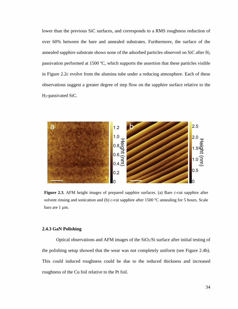
34
lower than the previous SiC surfaces, and corresponds to a RMS roughness reduction of
over 60% between the bare and annealed substrates. Furthermore, the surface of the
annealed sapphire substrate shows none of the adsorbed particles observed on SiC after H2
passivation performed at 1500 ºC, which supports the assertion that these particles visible
in Figure 2.2c evolve from the alumina tube under a reducing atmosphere. Each of these
observations suggest a greater degree of step flow on the sapphire surface relative to the
H2-passivated SiC.
Figure 2.3. AFM height images of prepared sapphire surfaces. (a) Bare c-cut sapphire after
solvent rinsing and sonication and (b) c-cut sapphire after 1500 ºC annealing for 5 hours. Scale
bars are 1 µm.
2.4.3 GaN Polishing
Optical observations and AFM images of the SiO2/Si surface after initial testing of
the polishing setup showed that the wear was not completely uniform (see Figure 2.4b).
This could induced roughness could be due to the reduced thickness and increased
roughness of the Cu foil relative to the Pt foil.

35
Figure 2.4. AFM height images of SiO2/Si, GaN/Si, and single-crystal GaN surfaces. (a) SiO2/Si
before and (b) after test polishing on Cu foil, (c) GaN/Si before and (d) after electrochemical
polishing on Pt foil, and (e) single-crystal GaN before and (f) after electrochemical polishing on
Pt foil. All scale bars are 1 µm.
Electrochemical polishing experiments with increasing pressures and increasing
polishing times show no reconstructed surface on the GaN/Si substrate, as measured by
AFM. The only visible changes in the GaN/Si samples were increasing size and number of
etch pits on the surface, with some areas showing large swaths of decreased height, likely
due to entire regions of GaN being removed from the Si substrate beneath (Figure 2.4d).
Due to these apparent problems with the stability of the GaN layer of GaN/Si substrates, I
decided to repeat the electrochemical polishing using a single crystal of GaN. While GaN
is not a cost-effective alternative to other CVD growth substrates, successful
electrochemical polishing would allow for another reconstructed, crystalline substrate to

36
pursue the high-quality, large-area CVD growth of monolayer TMDCs. After cleaning and
mounting the GaN substrate on the polishing apparatus, polishing was performed at the
calibrated pressure for a total of one hour. AFM analysis shows that no surface
reconstruction was observed on these GaN substrates. The only change observed on the
surface after polishing was the presence of deep trenches, likely mechanically etched by
the Pt foil.
Given the unsuccessful nature of these electrochemical polishing attempts, the use
of GaN as a growth substrate was not pursued. It was concluded that previously reports of
electrochemical polishing of GaN on Pt foil likely require the use of a highly sensitive and
adjustable polishing setup to successfully induce the desired surface reconstruction.
2.4.4 CVD Growth of MoS2 on Various Substrates
Scanning electron microscope (SEM) images of CVD-grown ML MoS2 on SiO2/Si
show sharp, symmetrical, triangular flakes (Figure 2.5), but there is no detectable
alignment between grains. This lack of rotational alignment is expected for growth on an
amorphous surface oxide like SiO2/Si. However, this also limits the use of SiO2/Si as a
substrate for large area ML MoS2, because rotational misalignment prevents grain
coalescence and promotes the formation of defects between merging grains. MoS2 grown
on c-cut sapphire shows similarly sharp and symmetrical grains, but the flakes in this case
are significantly larger, up to 50 µm in length. This increase in flake length is likely a result
of the hexagonal surface oxide of the Al2O3 allowing for van der Waals epitaxy through
the coincident hexagonal superlattice of (3 × 3) MoS2 on (2 × 2) Al2O3. AFM images
confirm that the MoS2 flakes on both substrates are truly monolayer in nature (Figure

37
2.5c−d), showing flake heights of approximately 7 Å. Furthermore, many ML MoS2 flakes
on sapphire are visibly aligned with the surface terraces visible in the sapphire after growth,
suggesting that van der Waals epitaxy is present in this MoS2 growth.
Figure 2.5. SEM and AFM images of CVD-grown ML MoS2. ML MoS2 is grown on (a) 90 nm
SiO2/Si and (b) c-cut sapphire. AFM height images of MoS2 grown on (c) SiO2/Si and (d) c-cut
sapphire show that the MoS2 is monolayer.
ML MoS2 grown on annealed sapphire substrates shows a completely different
morphology than that grown on SiO2/Si or non-annealed sapphire (see Figure 2.6). Optical
images show linear patterns of light contrast, and these samples show both the Raman and
photoluminescence (PL) peaks for MoS2, indicating the sample is monolayer in nature.

38
While AFM height analysis shows no distinguishable height differences corresponding to
MoS2, MoS2 is confirmed to be present by lateral force microscopy (LFM). LFM allows
for identification of materials with different magnitudes of surface adhesion, because these
materials tilt the AFM cantilever laterally to different degrees, which is detectable by the
instrument. LFM images in Figure 2.6d show dark regions of lower friction, which
correspond to the smooth, van der Waals surfaces of the MoS2 layers. The MoS2 flakes
grown in this system are aligned along the terrace edges of the annealed sapphire and seem
to be confined to these terraces, with few flakes spreading across multiple terrace steps. It
seems that the energetic penalty of growing over an edge of an annealed sapphire terrace
is too large to support uniform, large-area MoS2 growth, so the MoS2 grows in the confined
regions between terrace edges. Because of this, I used non-annealed c-cut sapphire wafers
for all subsequent MoS2 and TMDC growths on sapphire.

39
Figure 2.6. CVD growth of MoS2 on annealed sapphire. (a) Optical image, (b) PL spectrum
showing the additional presence of MoS2 Raman peaks, (c) AFM height image, and (d) LFM
friction image, acquired simultaneously with the height image, of CVD MoS2 on annealed
sapphire.
Alongside these experiments of CVD MoS2 on annealed sapphire, I performed
MoS2 growths on bare 4H-SiC(0001). The optimized CVD growth of MoS2 growth on SiC
results in triangular flakes similar to those grown on SiO2/Si. However, many MoS2 flakes
feature additional MoS2 nucleated domains on the surface of the flakes, as visible in SEM
images (Figure 2.7a). In the process of optimizing the CVD growth of MoS2 on 4H-SiC,
some experiments resulted in freestanding particles and platelets (Figure 2.7b). Some of
these platelets appear to have different material contrast on the interior and exterior (Figure
2.7c), leading to the identification of these as core/shell plates comprised of MoO2 cores

40
and MoS2 shells. This intermediate growth condition, in which both MoS2 and core/shell
plates are observed, was also achieved on c-cut sapphire substrates (Figure 2.7d), but these
samples are notably more difficult to image in SEM, given that sapphire is an insulating
substrate and is prone to charging effects. Given the intriguing core/shell nature of these
plates and their apparent alignment, I subsequently optimized the CVD growth process to
select for these platelets grown on SiC and analyzed their composition and structure. The
growth and mechanism of these MoO2/MoS2 core/shell plates will be discussed in further
detail in Chapter 4.
Figure 2.7. SEM images of MoS2 and MoO2/MoS2 growths on 4H-SiC. (a) CVD growth of MoS2
on 4H-SiC, (b) CVD growth of MoS2 on 4H-SiC using slightly altered reaction conditions,
showing presence of freestanding plates, (c) core/shell plate with truncated corner, showing the
core/shell nature of these plates, and (d) MoS2 and core/shell plates as grown on c-cut sapphire.

41
2.4.5 NbS2 CVD Growth
Representative NbS2 flakes synthesized on c-cut sapphire from oxide precursor can
be seen in Figure 2.8. Optical images show symmetrical, triangular flakes with bright
optical contrast. This contrast is significantly brighter than other mono- or few-layer
TMDCs, which implies that the materials are much thicker. This is supported by AFM
height image and profile traces, which show that the flakes are ∼50 nm in thickness. The
Raman spectra of representative NbS2 flakes synthesized from Nb2O5 show the E1 and E2
modes for NbS2, but none of the other expected Raman modes are present. The absence of
other Raman modes in these NbS2 flakes is likely due to a large concentration of defects,
but more research would need to be done to confirm this.

42
Figure 2.8. NbS2 flakes synthesized from the oxide-based CVD method. (a) Optical image, (b)
Raman spectrum, (c) and AFM height image of representative oxide-based NbS2 flakes. (d) AFM
profile trace along the dashed line in (c).
Many optimization experiments were performed with the intention of decreasing
the thickness of these bulk-like NbS2 flakes, but ultimately none were successful. The
thickness of these flakes is likely related to the extreme temperatures required to evolve
the Nb2O5−x precursor. I then decided to pursue the growth of 2D NbS2 using a significantly
more volatile chloride-based precursor, NbCl5.
Representative NbS2 flakes synthesized on c-cut sapphire from chloride precursor
can be seen in Figure 2.9. Optical images show that many flakes have rough, asymmetrical
morphologies with stripes of higher optical contrast than most of the flake. The low contrast
of most of the flake surface is expected for flakes that are mono- or few-layer, whereas the
high contrast of the stripe region likely indicates local regions of multi-layer NbS2. The

43
localization of these multi-layer stripes and the rough, asymmetrical morphology of the
flakes are likely due to poor surface diffusion at the reduced temperature of 900 ºC. Raman
spectra of these flakes clearly show all expected Raman modes for 3R NbS2, but additional
structural analysis is needed to confirm the phase (see Section 5.4.3). AFM height images
and profile traces show that these flakes are ∼2 nm in height, indicative of few-layer NbS2
(∼3−4 layers). Furthermore, the surface of the flakes are somewhat rough, with apparent
grain boundaries and gaps in the flake structure. This surface structure is likely a result of
insufficient surface diffusion and in-situ etching from residual chlorine-based species
resulting from the use of NbCl5 precursor.
Figure 2.9. NbS2 flakes synthesized from the chloride-based CVD method. (a) Optical image,
(b) Raman spectrum, (c) and AFM height image of representative chloride-based NbS2 flakes.
(d) AFM profile trace along the dashed line in (c).

44
With this data, I have demonstrated the successful CVD growth of few-layer NbS2
on c-cut sapphire substrates. However, it is apparent that the resulting flakes from both
techniques are not nearly as thin or uniform as those of other TMDCs I have grown,
including the ML MoS2 described above and the ML WS2 that will be described in the
following chapters. The quality of both the oxide-based and the chloride-based NbS2 is
likely limited by the precursor in each of these growth schemes. In the oxide-based growth,
the low vapor pressure of Nb2O5 requires the use of sufficiently high reaction temperatures
at which bulk NbS2 flakes are unavoidable. In the chloride-based growth, the high
reactivity of NbCl5 and other chlorine-based byproducts likely results in film etching that
appears to compete with the surface diffusion and flake growth. To perform more uniform,
high-quality growth of ML NbS2, future experiments should use alternative niobium-
containing precursors, as they may allow for more control over the growth morphology.
2.4.6 WSe2 CVD Growth and Selenization
Initial growths of ML WSe2 can be seen in Figure 2.10. Optical images show clear
triangular flakes, and representative Raman and PL spectra show Raman peaks and strong
PL signal expected for monolayer WSe2. These WSe2 flakes are further confirmed to be
monolayers by AFM height imaging. Height profiles show that the flakes have thickness
of ∼7 Å, indicative of the monolayer thickness. However, the as-grown WSe2 monolayers
are quite air sensitive, generally decomposing in less than one day in air. The beginning
stages of this decomposition can be observed in the AFM image in Figure 2.10d, indicated
by the small bumps on the WSe2 surface and the larger particles at the WSe2 edges. Thus,

45
I performed experiments to stabilize the as-grown WSe2 through the use of a selenization
procedure.
Figure 2.10. CVD-grown ML WSe2. (a) Optical image, (b) Raman spectrum, (c) PL spectrum,
and (d) AFM height image of monolayer WSe2. Inset profile trace in (d) corresponds with the
white dashed line in (d).
The results of WSe2 selenization can be seen in Figure 2.11. After selenization, the
WSe2 flakes appear to be quite stable in air, retaining shape and Raman/PL character after
more than 20 days in air. However, selenization appears to induce some undesirable effects
in the resulting WSe2 morphology. The resulting flakes show asymmetrical shape, and
some higher-contrast regions are visible among the otherwise uniform flake surface in

46
optical images. These higher-contrast regions are corroborated in AFM images, appearing
to show local few-layer thicknesses of ∼3 nm, compared to the otherwise uniformly
monolayer ∼7 Å thickness. Despite the non-ideal flake morphologies of these selenized
WSe2 flakes, they should prove suitable for future applications and study.
Figure 2.11. ML WSe2 after selenization. (a) Optical image, (b) Raman spectrum, (c) PL
spectrum, and (d) AFM height image of monolayer WSe2 after selenization. Inset profile trace
in (d) corresponds with the white dashed line in (d).
2.5 Conclusion
Here, I demonstrate the investigation into the preparation of a variety of
synthetically relevant substrate surfaces, including 4H-SiC, c-cut sapphire, SiO2/Si,
GaN/Si, and GaN. These substrate surfaces were modified with passivation, annealing, and

47
electrochemical polishing methods, respectively. 4H-SiC was shown to exhibit a small
amount of step flow under moderate passivation conditions, but higher temperature
passivation resulted in no observable step flow due to obstruction by contaminants from
the tube under the high-temperature, reducing environment. c-cut sapphire shows a great
deal of step flow after high-temperature ambient annealing, with the resulting terraces
showing very smooth surfaces and large step heights. SiO2/Si, GaN/Si, and GaN show
some rough etching as a result of the polishing, but no surface reconstruction or smoothing
is observed. Few of the surface preparation methods discussed here resulted in ideal
substrates for large-area TMDC growth, but they demonstrate ways in which substrate
surfaces can be modified and tailored for specific applications.
After preparing these substrate surfaces, some were used for the CVD growth of a
variety of 2D TMDCs, including MoS2, NbS2, and WSe2. MoS2 growth on bare SiO2/Si
and c-cut sapphire substrates show large area, monolayer flakes in both cases, but MoS2
grown on sapphire shows that the grains are generally aligned to the surface terraces of the
substrate. MoS2 grown on annealed c-cut sapphire shows irregular, asymmetrical flakes
confined to terrace step edges. MoS2 grown on 4H-SiC shows rotationally disordered
grains with few-layer regions, and with some minor synthetic modifications, the presence
of core-shell plates, which will be discussed in more detail in Chapter 4. NbS2 grown on c-
cut sapphire via Nb2O5 precursor show bulk-like flakes, whereas NbS2 grown via NbCl5
precursor show asymmetrical but few-layer flakes. WSe2 grown on c-cut sapphire shows
sharp, symmetrical, monolayer flakes that degrade quickly in air. Subsequent selenization
of these WSe2 flakes improves their stability in air and retains monolayer thickness in some
regions, despite inducing regions of few-layer thickness in other regions. With this data, I

48
show that these high-quality materials can be reproducibly synthesized through
optimization and synthetic control on relevant substrates. It is also demonstrated that the
choice of substrate and surface preparation can have a dramatic effect on the resulting
TMDC growth. The TMDCs grown here will be extended to a variety of novel
heterostructures in the subsequent chapters of this dissertation.

49
Chapter 3
2D Material Semiconductor Heterostructures

50
3.1 Preface
Atomically thin, TMDC semiconductor heterostructures show promise for next-
generation electronics and optoelectronics, and control of these heterostructures without
interfacial contamination is essential for utility. Here, I describe a controllable, two-step
CVD process for lateral and vertical heteroepitaxy between ML WS2 and ML MoS2 on c-
cut sapphire. Lateral and vertical heteroepitaxy can be selectively achieved in this system
by careful control of the ML MoS2 growth that is used as a 2D seed crystal. Ultraclean
MoS2 monolayers are grown using hydrogen as a carrier gas, which enables lateral
heteroepitaxial growth of ML WS2 from the MoS2 edges, thereby creating atomically
coherent, in-plane WS2/MoS2 heterostructures. When no hydrogen is used, the as-grown
ML MoS2 is decorated with small particles along the edges, inducing vertical
heteroepitaxial growth of ML WS2 on top of the MoS2 to form vertical WS2/MoS2
heterostructures. This lateral and vertical atomic layer heteroepitaxy steered by seed defect
engineering opens a new avenue toward atomically controlled fabrication of 2D
heterostructure architectures.
3.2 Introduction
3.2.1 Semiconductor Heterostructures
Semiconductor heterostructures are material systems in which two or more
semiconducting materials are directly interfaced. By nature of interfacing two different
semiconductors, the band structure position can be independently controlled in each
material, thereby offering new possibilities for device functionality. These materials can
align their bands in one of three different ways (Figure 3.1).70 In type I heterostructures,

51
the conduction band (CB) and valence band (VB) of one semiconductor entirely straddle
that of the CB and VB of the second. In type II heterostructures, the CB and VB of the first
semiconductor are staggered relative to the CB and VB of the second, such that the CB and
VB of one semiconductor are above the CB and VB of the other semiconductor but neither
VB is above either CB. In type III heterostructures, the CB and VB of one semiconductor
are above both the VB and CB of the other semiconductor, with no overlap between the
two band gaps. The relative and absolute positions of these bands dictate the properties of
the heterostructure and the applications for which the heterostructure can prove
technologically useful.
Figure 3.1. Schematic illustrating the band alignment of the three types of semiconductor
heterostructures.
3.2.2 2D Material Heterostructures
Heterostructures composed of 2D TMDCs show promise as building blocks for a
variety of device applications.2 2D semiconductor heterostructures are quite different than
3D semiconductor heterostructures because the 2D materials act both as the bulk material
and interface, simultaneously. This reduces the amount of charge displacement within each

52
layer, but allows for interesting possibilities in the context of band-structure engineering.71
Furthermore, the mechanical flexibility and low material thickness of 2D materials are
enticing in the context of novel device fabrication.
Some of the first 2D TMDC heterostructures were fabricated by micromechanical
exfoliation of bulk crystals followed by vertical stacking of the layers.72,73 Vertical stacking
of WS2/MoS2 or WSe2/MoS2 creates type II heterostructures, as described above, but the
electronic properties of these heterostructures are quite sensitive to many subtle details of
the transfer process, including twist angle and the presence of interfacial debris.72–75 It has
also been reported that both vertical and in-plane heterostructures of monolayer WS2/MoS2
can be grown via a single-step CVD process, which allows for a greater degree of control
over the heterostructure morphology and properties.76
3.2.3 MoS2/WS2 Ultraclean Heterostructures
Heteroepitaxy, as described in Chapter 2, can be used to grow in-plane TMDC
heterostructures unobtainable by any exfoliation or transfer-based techniques. In-plane
junctions created using this method have appealing optoelectronic properties, including a
linearly abrupt p−n junction.76 Previous reports of these heterostructures feature only a
single synthetic step, which limits the amount of control one can exert over important
physical features, such as particle size, shape location, and junction width.76,77 To this end,
a two-step process is desirable, as it could allow for patterned 2D heterostructures and
independent growth control of each individual material. Multi-step growth procedures such
as these have been reported for graphene and hexagonal boron nitride heterostructures.78–
82

53
Creating in-plane (lateral) heterostructures can be difficult due to challenges with
preventing contamination of the seed crystal. Adsorbates, defects, or particles persisting
after the growth of the first material can function as unintended nucleation sites when
depositing the second material and can induce additional material growth in undesirable
locations.83 Thus, a two-step process for fabricating lateral heterostructures composed of
monolayer WS2/MoS2 demands meticulous care in preparing clean surfaces and edges of
the 2D seed crystals.
We show that a two-step CVD process can be used to selectively achieve lateral
and vertical heteroepitaxy between monolayer WS2 and MoS2 through careful growth
control of monolayer MoS2 seed crystals. Including H2 in the carrier gas results in
ultraclean MoS2 monolayers. These ultraclean MoS2 flakes suppress the nucleation and
growth of additional vertical layers and facilitate the lateral heteroepitaxial growth of
monolayer WS2, culminating in atomically coherent in-plane WS2/MoS2 heterostructures.
Without the use of H2, CVD-grown MoS2 monolayers are decorated with small particles
along the edges. These particles nucleate vertical heteroepitaxial growth during subsequent
growth of WS2, thereby forming vertical WS2/MoS2 heterostructures with perfect
alignment. This work is reproduced with permission from Yoo, et al.84
3.3 Experimental
Ultraclean MoS2 monolayers were synthesized in a horizontal hot-wall three-zone
tube furnace (ThermoFisher Blue M, with only the center zone being heated), equipped
with a vacuum pump (Edwards RV-8) and mass flow controllers (MTI Corp.). An alumina
boat (50 × 20 × 20 mm, MTI Corp.) containing 400 mg MoO3 powder (99.999%, Acros

54
Organics) was placed at the center of the furnace in a 3-inch diameter quartz tube. A c-cut
sapphire substrate (MTI Corp.) was placed polished-face-up on an upside-down alumina
boat placed directly downstream from the boat containing MoO3 powder. 800 mg S powder
(99.999%, Alfa Aesar) was located upstream, maintained at a reduced temperature during
the reaction (approximately 280 ºC at the peak of the reaction). After loading, the tube was
evacuated to less than 100 mTorr, and Ar and H2 gases were supplied at rates of 20 and 4
sccm (standard cubic centimeters per minute), respectively. The reaction was carried out
under atmospheric pressure. The center of the furnace (and thus the substrate and MoO3
powder precursor) was heated to 710 ºC at a rate of 22 ºC/min and kept at 710 ºC for 5 min.
After the reaction, the furnace was rapidly cooled by opening the lid of the furnace. At this
point, the Ar gas flow was increased to 200 sccm, to purge any toxic vapors. The
experimental conditions for the growth of MoS2 monolayers decorated with particles are
the same as those for the growth of ultraclean MoS2 monolayers except that no H2 carrier
gas is used.
To synthesize WS2/MoS2 heterostructures, monolayer MoS2 grown on c-cut
sapphire was used as a substrate for the subsequent growth of WS2. 500 mg WO3 powder
(99.998%, Alfa Aesar) was placed at the center of the furnace in a 2-inch diameter quartz
tube. The substrate was placed a few centimeters downstream from the center of the furnace
and the sulfur powder was placed upstream (at temperatures of approximately 940 ºC and
160 ºC, respectively, during the peak of the reaction). Ar and H2 gases were introduced at
rates of 60 and 5 sccm, respectively, maintaining a chamber pressure of 350 mTorr during
the growth. The center of the furnace (and thus the WO3 powder precursor) was heated to
1050 ºC at a rate of 11 ºC/min and kept at 1050 ºC for 5 min. The furnace was rapidly

55
cooled down after the reaction by opening the lid of the furnace. In-plane WS2/MoS2
heterostructures were synthesized when ultraclean monolayer MoS2 on sapphire was used
as a substrate, while vertical WS2/MoS2 heterostructures were synthesized when the
monolayer MoS2 decorated with particles on sapphire was used as a substrate.
The atomic structure of the lateral heterostructure is characterized by Z-contrast
STEM imaging using an aberration-corrected STEM (FEI Titan G2) operated at an
accelerating voltage of 60 kV. Prior to imaging, samples were transferred onto transmission
electron microscopy (TEM) grids using a wet chemical transfer process. First, a 5%
solution of poly(methyl methacrylate) (PMMA, MW ∼996,000, Sigma Aldrich) in anisole
was spin-coated onto WS2/MoS2 heterostructures grown on c-cut sapphire (3000 rpm
rotation for 1 min). After coating, the sample was baked on a hot plate at 50 ºC for 10 min.
The underlying sapphire substrate was etched in a 30% aqueous solution of KOH (Fisher
Scientific) for several hours, etching the top layer of the substrate surface and delaminating
the substrate. The PMMA with adhered WS2/MoS2 heterostructures was then rinsed in
deionized water and transferred onto a TEM grid. To remove the PMMA film residue, the
sample was cleaned with ∼10 drops of acetone and then annealed in a tube furnace at
350 ºC with 100 sccm of H2 and Ar gas at atmospheric pressure. After subsequent loading
into the TEM, samples were annealed at 160 ºC for 4 hours under vacuum to avoid
hydrocarbon contamination.
AFM measurements were acquired using a Bruker Nanoscope V Multimode 8
scanning probe microscope in the Characterization Facility at the University of Minnesota.
Raman and photoluminescence spectra were acquired using a home-built Raman setup

56
using a 632.8 nm continuous wave laser focused through a 100× objective lens with a beam
power of ∼30−300 µm.
In this work, I performed the characterization of the MoS2/WS2 heterostructures via
AFM and KPFM, and HRTEM atomic diffusion analysis. I also contributed intellectually
to the realization of these experiments and have since replicated their results. Youngdong
Yoo performed the entirety of the synthesis of these heterostructures, as well as
characterization via AFM, Raman, PL, SEM, and TEM.
3.4 Results and Discussion
Figure 3.2 shows the comparison between triangular monolayer flakes of MoS2
grown with and without H2 included in the carrier gas stream. Under typical CVD
conditions (without H2), the edges of the MoS2 flakes are decorated by small particles, as
shown by AFM. Similar particles to those seen in our flakes have been observed in other
reports of MoS2 synthesis. The inclusion of 4 sccm H2 into the carrier gas stream during
the synthesis prompts the disappearance of these particles. The ultraclean nature of these
monolayer MoS2 flakes is confirmed by AFM height images and line profiles, which show
no presence of particles. In both cases (H2 included and excluded), the flakes are confirmed
to be monolayer by AFM, showing flake thicknesses of approximately 0.7 nm, consistent
with previous reports of monolayer MoS2.85–92 SEM analysis of ML MoS2 grown with and
without hydrogen is visible in Figure 3.3

57
Figure 3.2. Monolayer MoS2 crystals synthesized on c-cut sapphire without and with hydrogen
gas. AFM height images of monolayer MoS2 grown (a) without, and (b) with hydrogen,
respectively. (c,d) Height line profiles along the dotted white lines in (a) and (b), respectively.
PL intensity maps of monolayer MoS2 grown (e) without and (f) with hydrogen, respectively.
(g) PL and (h) Raman spectra of ultraclean monolayer MoS2. This figure is reproduced with
permission from Yoo, et al. J. Am. Chem. Soc. 2015, 137 (45), 14281–14287.84
The monolayer nature of the synthesized MoS2 seed crystals is also confirmed by
Raman spectroscopy. The Raman spectrum of MoS2 shows two characteristic peaks: the
out-of-plane vibration of the S atoms (A1) and the doubly degenerate in-plane vibrations
of the Mo and S atoms (E2).93 The energy of the phonons associated with these vibrational
modes changes with sample thickness, and thus the spectral separation of these two Raman
peaks has become a common tool for determining the number of layers in a given sample
of MoS2. In these samples, the MoS2 flakes exhibit a peak separation of 20.3 cm−1, which
is in good agreement with previous reports of monolayer MoS2 syntheses.

58
Figure 3.3. SEM images of monolayer MoS2 grown (a,b) with and (c,d) without hydrogen,
respectively. This figure is reproduced with permission from Yoo, et al. J. Am. Chem. Soc. 2015,
137 (45), 14281–14287.84
The MoS2 Raman spectrum shown in Figure 3.2h was acquired on resonance with
the B exciton absorption band. Resonance Raman spectra can exhibit spectral changes
including line-broadening, large fluorescence backgrounds, and additional non-zone-
centered modes. Additional modes are observed in the resonance spectra that are not visible
in the off-resonance Raman spectra.93,94 To obtain a more accurate measurement of the
separation between MoS2 Raman peaks, spectra were acquired using the off-resonance
excitation of a 514.5 nm continuous wave laser. These spectra show no spectral congestion,
increased signal-to-noise, and a MoS2 peak separation of 17 cm−1. The source of this
decreased splitting could be due to enhanced substrate interactions, but further study is

59
needed to confirm this. Raman spectra and Lorentz fitting for ML MoS2 can be seen in
Figure 3.4.
Figure 3.4. Raman spectra and Lorentz fitting results for monolayer MoS2. (a) Raman spectrum
of a monolayer MoS2 flake excited by a 632.8 nm HeNe laser. (b) Raman spectrum of a
monolayer MoS2 flake excited by a 514.5 nm Ar+ ion laser. This figure is reproduced with
permission from Yoo, et al. J. Am. Chem. Soc. 2015, 137 (45), 14281–14287.84
PL spectroscopy confirms that the inclusion of H2 gas leads to a cleaner and more
homogeneous material. Figure 3.2g shows a PL spectrum acquired at room temperature on
ultraclean monolayer MoS2, exhibiting a strong A-exciton peak at 667 nm stemming from
the direct band gap of MoS2.21,95 PL intensity maps of the emission from the A exciton of
monolayer MoS2 grown without H2 gas is spatially heterogeneous and shows a faint ∼1 µm
ribbon with reduced intensity, due to partial quenching of the PL. PL intensity maps of
MoS2 grown with H2 are highly uniform, indicating uniform chemical composition and
electronic structure.

60
Figure 3.5. In-plane heteroepitaxial WS2/MoS2 monolayers synthesized from monolayer MoS2
grown with hydrogen. (a) Atomic model of an in-plane heteroepitaxial junction between MoS2
and WS2. (b) SEM image and (c) optical image of the in-plane heteroepitaxial monolayers. (d,e)
PL intensity mapping of WS2 and MoS2 from the in-plane heteroepitaxial monolayer,
respectively. (f) PL and (g) Raman spectra taken from the points marked by 1−2 in (c). (h) AFM
height image of the in-plane heteroepitaxial monolayer, with the height line profile in (i) acquired
along the dotted white line in (h). This figure is reproduced with permission from Yoo, et al. J.
Am. Chem. Soc. 2015, 137 (45), 14281–14287.84
c-cut sapphire is an ideal choice of substrate, because the surface is atomically flat
and it has been previously shown to improve the crystallinity of CVD-grown MoS2 and
WS2.96,97 Furthermore, the lattice mismatch between the sapphire substrate and supercells

61
of MoS2 and WS2 is quite low – only 0.42% and 0.64% for (3 × 3) MoS2 and (3 × 3) WS2
supercells on (2 × 2) sapphire(0001), respectively. The MoS2/WS2 lateral heterostructures
are oriented along two preferential directions on the substrate, thereby indicating that the
heteroepitaxial monolayers are grown with van der Waals epitaxy on the c-cut sapphire
surface.
PL spectra acquired from the inner triangle and outer ribbon of lateral
heterostructures (Figure 3.5f) show strong PL signals from MoS2 and WS2, respectively,
due to emission from the lowest energy A excitons of the respective TMDCs.21,95,98,99 The
interface region between the two TMDCs shows PL signal from both WS2 and MoS2, as
expected. PL intensity maps of the A exciton from WS2 and the A exciton from MoS2
demonstrate that the in-plane junctions are monolayer and have mutually exclusive
domains, with no MoS2 PL present in the WS2 region and vice versa. The PL intensity
variations visible in the maps could be due to nonuniform strain induced by the lattice
mismatch between the substrate and MoS2/WS2 or the difference in thermal expansion
coefficients between the substrate and MoS2/WS2.100,101 These effects could also lead to
the variation of Raman peak positions. In accordance with the PL maps, Raman spectra of
the inner triangle of the lateral heterostructures show E12 and A1 peaks of MoS2, and Raman
spectra of the outer ribbon show peaks corresponding to the 2LA and A1 phonons of
monolayer WS2. Raman signals of both WS2 and MoS2 are observed in the junction region.
Raman peak position maps of the 2LA and A1 modes of WS2 from in-plane heterostructures
are also visible in Figure 3.6.

62
Figure 3.6. (a,b) Raman peak position mapping at the 2LA and A1 modes of WS2 from in-plane
heterostructures, respectively. This figure is reproduced with permission from Yoo, et al. J. Am.
Chem. Soc. 2015, 137 (45), 14281–14287.84
AFM height images of the in-plane heterostructure and line profiles across these
flakes show that the MoS2/WS2 heterostructures are indeed monolayer, with both materials
in the same plane and each possessing a height of 0.7 nm (Figure 3.5h). The lateral force
microscopy (LFM) friction image clearly shows the lateral junction between the MoS2 and
WS2 domains, likely due to subtle friction differences in the resulting TMDCs (Figure 3.7).
Furthermore, Kelvin probe force microscopy (KPFM) data confirms that as-synthesized
heterostructures have high-quality lateral junctions (Figure 3.8), with the MoS2 and WS2
domains showing clear contrast corresponding to the difference in work function between
the two materials.
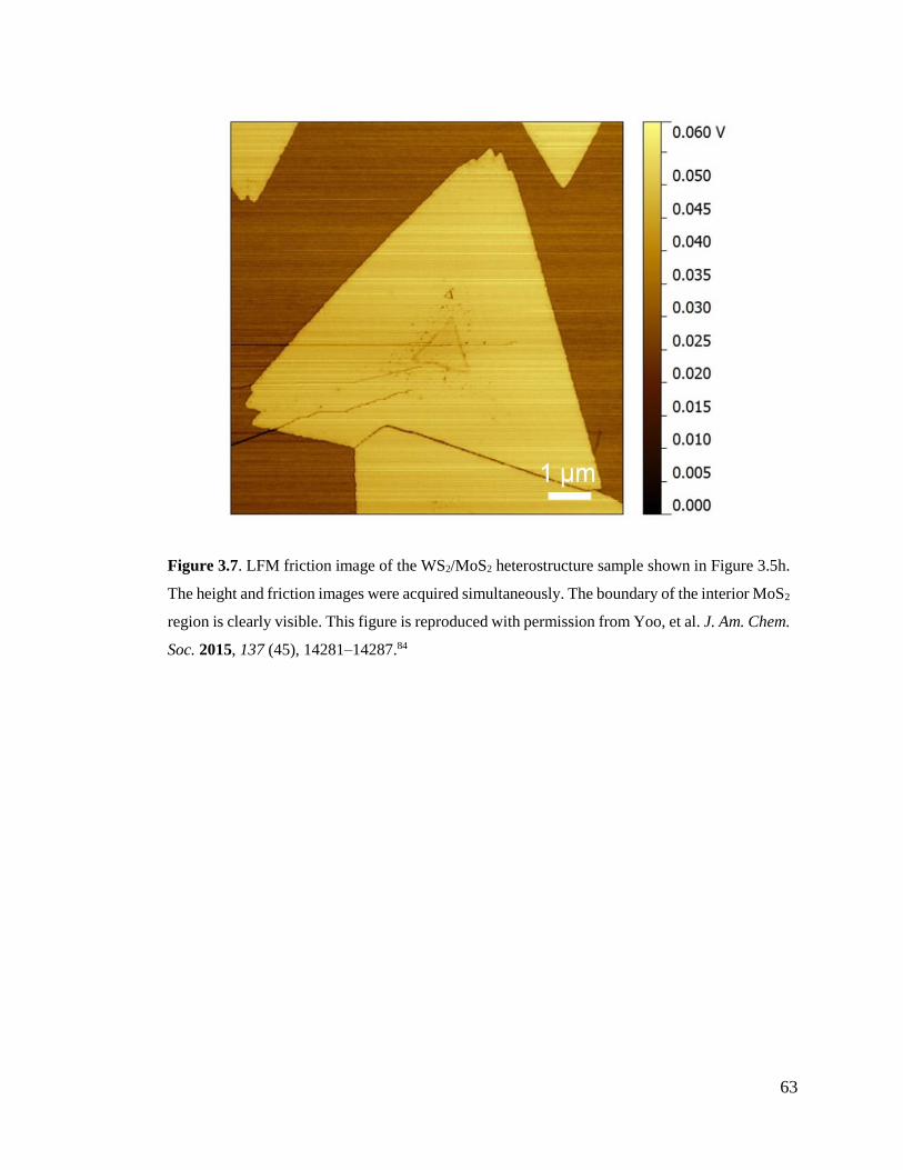
63
Figure 3.7. LFM friction image of the WS2/MoS2 heterostructure sample shown in Figure 3.5h.
The height and friction images were acquired simultaneously. The boundary of the interior MoS2
region is clearly visible. This figure is reproduced with permission from Yoo, et al. J. Am. Chem.
Soc. 2015, 137 (45), 14281–14287.84
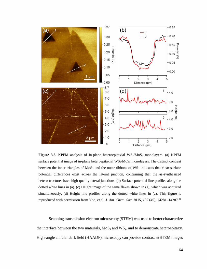
64
Figure 3.8. KPFM analysis of in-plane heteroepitaxial WS2/MoS2 monolayers. (a) KPFM
surface potential image of in-plane heteroepitaxial WS2/MoS2 monolayers. The distinct contrast
between the inner triangles of MoS2 and the outer ribbons of WS2 indicates that clear surface
potential differences exist across the lateral junction, confirming that the as-synthesized
heterostructures have high-quality lateral junctions. (b) Surface potential line profiles along the
dotted white lines in (a). (c) Height image of the same flakes shown in (a), which was acquired
simultaneously. (d) Height line profiles along the dotted white lines in (a). This figure is
reproduced with permission from Yoo, et al. J. Am. Chem. Soc. 2015, 137 (45), 14281–14287.84
Scanning transmission electron microscopy (STEM) was used to better characterize
the interface between the two materials, MoS2 and WS2, and to demonstrate heteroepitaxy.
High-angle annular dark field (HAADF) microscopy can provide contrast in STEM images

65
of these heterostructures based on the scattering cross-sections for Mo and W atoms (also
called Z contrast).102 Low-magnification HAADF-STEM images of in-plane
heteroepitaxial monolayers show that the junction between the outer ribbon of WS2 and the
inner triangle of MoS2 is visible but with relatively low contrast. The magnified image of
the dotted orange square in Figure 3.9a shows a clear contrast difference between MoS2
and WS2 (Figure 3.9b). The image intensity at a given point in these HAADF-STEM
images is determined by the spatial average atomic number and the thickness of the sample.
Because the atomic number of WS2 is larger than that of MoS2, the WS2 appears brighter
(higher image intensity) than the MoS2 in dark-field imaging. Atomic-resolution HAADF-
STEM imaging (Figure 3.9c) with associated fast Fourier transform (FFT) pattern of the
junction region (inset) of the lateral heterostructure shows the atomically sharp junction
between WS2 and MoS2 along a zig-zag direction. Even though the WS2 growth occurs at
a high temperature (higher than that of the MoS2 growth), only minor annealing and
elemental mixing is observed across the interface between WS2 and MoS2. Of the elemental
mixing that occurs, a larger concentration of W is substituted into the MoS2 lattice than
that of Mo substituted into the WS2 lattice. This will be discussed in more detail later in
this chapter.

66
Figure 3.9. Z-Contrast HAADF-STEM images of the in-plane heteroepitaxial WS2/MoS2
monolayer. (a) Low-magnification HAADF-STEM image of the in-plane heteroepitaxial
monolayer. (b) Magnified image of the dotted orange square in (a). (c) Atomic resolution
HAADF-STEM image and its corresponding FFT pattern (inset) of the junction region of the in-
plane heteroepitaxial monolayer. (d,e) Atomic-resolution HAADF-STEM images and
corresponding FFT patterns (inset) of the MoS2 region and the WS2 region, respectively, of the
in-plane heteroepitaxial monolayer. This figure is reproduced with permission from Yoo, et al.
J. Am. Chem. Soc. 2015, 137 (45), 14281–14287.84

67
The FFT patterns of the MoS2/WS2 heterostructure show only one set of hexagonal
spots, demonstrating that the WS2 grows outward from the MoS2 edges with lattice
coherence, likely due to the relatively small lattice mismatch between WS2 and MoS2
(0.22%). Atomic-resolution HAADF-STEM images and corresponding FFT patterns of
MoS2 and WS2 regions show clear hexagonal lattices without any substituted atoms. The
orientation of the FFT patterns of the WS2 region is the same as that of the MoS2 region,
further confirming the lattice coherence across the WS2/MoS2 boundary.
When WS2 is grown using the particle-decorated MoS2 monolayers as 2D seed
crystals, vertically stacked WS2/MoS2 heterostructures are created. SEM imaging of these
vertical heterostructures also shows a ribbon of WS2 around the edge of the heterostructure
region (Figure 3.10 and 3.11). These structures are confirmed to be vertically stacked by
PL and Raman spectroscopy and AFM imaging. PL and Raman spectra taken from the
center and edge of the vertical heterostructures show PL and Raman peaks from both WS2
and MoS2. The vertical heterostructures show relatively weak PL signal because the PL is
quenched by charge transfer between the WS2 and MoS2 layers.72,103 The small triangular
flakes visible in close proximity to the vertical heterostructures are identified as WS2
monolayers by PL and Raman spectroscopy. These triangular particles exhibit a strong
WS2 PL signal due to the direct band gap of monolayer WS2, and the Raman spectrum
shows only WS2 peaks (no evidence of MoS2). AFM height images and line profiles show
that the vertical WS2/MoS2 heterostructures have a thickness of about 1.4 nm and the
monolayer WS2 ribbons and triangular domains have a thickness of about 0.7 nm.

68
Figure 3.10. Vertical WS2/MoS2 heterostructures synthesized from monolayer MoS2 grown
without hydrogen. (a) SEM image of the vertical heterostructures. (b) PL and (c) Raman spectra
acquired at points marked 1−3 in the inset in (b). The inset in (b) is an optical microscope image
of a vertical heterostructure. (d) AFM height image of a vertical heterostructure. (e) Height line
profile along the dotted white line in (d). (f) Bright-field TEM image of the vertical
heterostructure. (g) HRTEM image of the dotted red square in (f) with corresponding FFT
patterns of the WS2 region and the WS2/MoS2 region, respectively. (h) SAED pattern of the
vertical heterostructure. This figure is reproduced with permission from Yoo, et al. J. Am. Chem.
Soc. 2015, 137 (45), 14281–14287.84
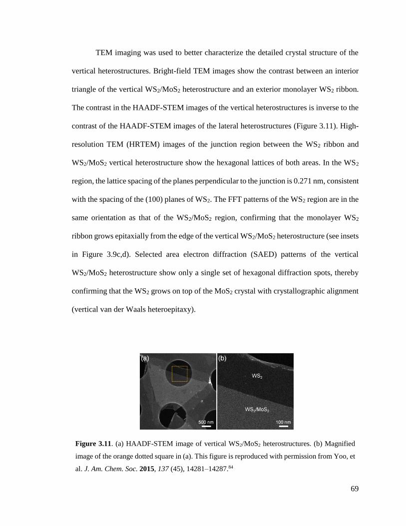
69
TEM imaging was used to better characterize the detailed crystal structure of the
vertical heterostructures. Bright-field TEM images show the contrast between an interior
triangle of the vertical WS2/MoS2 heterostructure and an exterior monolayer WS2 ribbon.
The contrast in the HAADF-STEM images of the vertical heterostructures is inverse to the
contrast of the HAADF-STEM images of the lateral heterostructures (Figure 3.11). High-
resolution TEM (HRTEM) images of the junction region between the WS2 ribbon and
WS2/MoS2 vertical heterostructure show the hexagonal lattices of both areas. In the WS2
region, the lattice spacing of the planes perpendicular to the junction is 0.271 nm, consistent
with the spacing of the (100) planes of WS2. The FFT patterns of the WS2 region are in the
same orientation as that of the WS2/MoS2 region, confirming that the monolayer WS2
ribbon grows epitaxially from the edge of the vertical WS2/MoS2 heterostructure (see insets
in Figure 3.9c,d). Selected area electron diffraction (SAED) patterns of the vertical
WS2/MoS2 heterostructure show only a single set of hexagonal diffraction spots, thereby
confirming that the WS2 grows on top of the MoS2 crystal with crystallographic alignment
(vertical van der Waals heteroepitaxy).
Figure 3.11. (a) HAADF-STEM image of vertical WS2/MoS2 heterostructures. (b) Magnified
image of the orange dotted square in (a). This figure is reproduced with permission from Yoo, et
al. J. Am. Chem. Soc. 2015, 137 (45), 14281–14287.84

70
The in-plane growth of WS2 ribbons around the monolayer MoS2 is thought to be
kinetically controlled, because vertical heterostructures are known to be more
thermodynamically stable than in-plane heterostructures.76 The mechanisms for the growth
of MoS2 and WS2 monolayers from their respective oxide precursors are effectively the
same and well accepted in the literature. Thermal reduction of the transition metal trioxide
precursor results in a volatile suboxide cluster, which can then adsorb onto, diffuse along,
and desorb from the substrate.104–106 This occurs until the suboxide cluster encounters a
nucleation site, where it will subsequently sulfurize to form MoS2 or WS2. The suboxide
clusters can be supplied to the MoS2 seed flakes by direct impingement from the vapor or
by surface diffusion from the substrate. It has been previously reported that surface
diffusion can be the major factor under high flux conditions, whereas direct impingement
can be the major factor under low flux conditions.107 For lateral growth of WS2 ribbons
around monolayer MoS2, suboxide clusters supplied by surface diffusion are the largest
contribution to the growth, because the anisotropic flow of material can induce the
anisotropic material growth.108 Thus, all WS2 growths described above were performed
under high-flux conditions. In contrast, vertical WS2/MoS2 heterostructures possess no
WS2 ribbons under low flux conditions (Figure 3.12). Under kinetically controlled reaction
conditions like those shown here, monolayer WS2 grows laterally from the edges of
monolayer MoS2, because these edge sites are the only sites active for nucleation when
ultraclean MoS2 monolayers are used as seeds.109 When particle-decorated MoS2
monolayers are used as seeds, particles on the MoS2 surface can serve as additional
nucleation sites, which leads to the formation of WS2/MoS2 vertical heterostructures with
a ribbon of monolayer WS2.

71
Figure 3.12. SEM, PL, and Raman analysis of vertical WS2/MoS2 heterostructures from low-
flux conditions with no WS2 ribbons. (a,b) SEM images of vertical WS2/MoS2 heterostructures
possessing no WS2 ribbons synthesized from monolayer MoS2 grown without hydrogen under
low flux conditions. The temperatures of WO3 powder and MoS2 seed crystals were about 960 °C
and 940 °C, respectively. (c) PL spectra of the vertical heterostructure (red curve), monolayer
MoS2 (blue curve), and monolayer WS2 (green curve). (d) Raman spectra of the vertical
heterostructure (red curve), monolayer MoS2 (blue curve), monolayer WS2 (green curve), and
the sapphire substrate (black curve). This figure is reproduced with permission from Yoo, et al.
J. Am. Chem. Soc. 2015, 137 (45), 14281–14287.84
The cleanliness of the MoS2 seed flakes dictates the ability to control the
competitive growth between lateral and vertical heterostructures. The small particles on
the surface and edges of the MoS2 synthesized without H2 (Figure 3.2a) should largely be
MoS2 formed by sulfurization of small molybdenum suboxide clusters, which are
continually supplied to the substrate during the reaction. Most of the suboxide clusters

72
contribute to the growth of monolayers or desorb from the substrate due to the high
substrate temperature, but some of the suboxide clusters will aggregate and form stable
molybdenum oxide particles. During this process, the edge regions of the monolayer MoS2
can serve as preferential nucleation sites, because the edge regions have previously been
shown to be sulfur-deficient when no H2 is used.110 These molybdenum oxide particles will
subsequently react with sulfur vapor to form small particles of MoS2. The stability of the
molybdenum suboxide particles is lowered in the presence of a highly reducing gas, such
as H2. The reduction of suboxide particles by H2 will thereby revolatilize the precursors,
leaving the basal plane of the MoS2 flake clean of debris. Furthermore, we believe that
monolayer MoS2 synthesized with H2 has highly homogeneous edges without sulfur
deficiencies, because H2 has been previously shown to drastically improve the quality of
monolayer TMDC edges.111,112
The TEM images displayed in Figure 3.9 and Figure 3.13 show atomic resolution
of the individual transition metals in each material. This resolution allows for the extraction
of important details regarding the local diffusion and atomic mixing across the MoS2/WS2
interface. It can be qualitatively seen in a HRTEM image of the interface, such as Figure
3.13a, that more W dopant atoms are visible in the MoS2 lattice than Mo atoms in the WS2
lattice. However, the quantitative nature of this elemental mixing and dopant diffusion
could provide a better picture of the growth process during the WS2 growth step. To assess
the quantitative diffusion of W and Mo atoms across the MoS2/WS2 lateral heterostructure
interface, I wrote a MATLAB script (see Appendix A) to count and plot the W and Mo
atomic concentration across the MoS2/WS2 interface. The results of this analysis on a
representative HRTEM image can be seen in Figure 3.13b.

73
Figure 3.13. HRTEM of MoS2/WS2 lateral interface and diffusion quantification. (a) HRTEM
image of MoS2/WS2 lateral heterostructure interface and (b) plot of the concentration of W and
Mo atoms as a function of distance from the interface pictured in (a). In this plot, the blue circles
and trace represent W and the red circles and trace represent Mo.
The W inclusions in the MoS2 lattice are present more than 25 nm from the
interface, whereas the Mo inclusions in the WS2 lattice seem to be minimal beyond 10 nm
from the interface. Furthermore, the concentration of W inclusions in the MoS2 lattice
remains greater than the concentration of Mo inclusions in the WS2 lattice at any given
respective position from the interface. This data suggests that W diffuses into the MoS2
crystal to a significant degree during the WS2 growth step, likely filling vacancies and
defects that form in the MoS2 as a result of the high-temperature, reducing WS2 growth
conditions. This data also suggests that some Mo diffuses away from the crystal edge and
becomes incorporated into the WS2 ribbon during the WS2 growth step, but the
concentration of Mo that is incorporated into the WS2 ribbon is much lower than W that is
incorporated into the MoS2 crystal. These observations could be a result of relatively large

74
binding energies of MoS2 units within the MoS2 crystal, or a locally greater vapor-phase
concentration of WO3–x above the substrate surface during the WS2 growth step, relative
to any Mo-containing species.
3.5 Conclusion
In summary, by carefully controlling contamination and defects present in the 2D
seed crystals, lateral and vertical heteroepitaxy between monolayer WS2 and MoS2 can be
selectively achieved on c-cut sapphire substrates. Hydrogen gas plays an important role in
removing small particles contaminating MoS2 monolayer seeds. When H2 is used as a
carrier gas, ultraclean MoS2 monolayers are synthesized, and can thereafter be used as
seeds for lateral heteroepitaxial growth of monolayer WS2 to form atomically coherent and
sharp in-plane, lateral WS2/MoS2 heterostructures. When no hydrogen is used, particle-
decorated MoS2 monolayers are obtained, which serve as seeds for vertical heteroepitaxial
growth of monolayer WS2 and the formation of vertical WS2/MoS2 heterostructures.
This two-step synthesis serves as a building block for making abrupt junctions
between 2D materials. By controlling the cleanliness of the 2D seed, we can limit the
growth of additional 2D materials in subsequent growth steps to the edges of the 2D seed.
This scheme can be utilized for many 2D heterostructures, including patterned junctions in
2D materials and as platforms for further explorations of the electronic and optical
properties of these materials.

75
Chapter 4
MoO2/MoS2 Core/Shell Nanoplates

76
4.1 Preface
Controlling the growth of 2D TMDCs is an important step toward utilizing these
materials for either electronics or catalysis. Here, we report a new surface-templated
growth method that enables the fabrication of MoO2/MoS2 and MoO2/MoTe2 core/shell
nanoplates epitaxially aligned on (0001)-oriented 4H-silicon carbide and sapphire
substrates. These heterostructures are characterized by a variety of techniques to identify
the chemical and structural nature of the interface. Scanning electron microscopy shows
that the nanoplates feature 3-fold symmetry indicative of epitaxial growth. Raman
spectroscopy indicates that the MoO2/MoS2 nanoplates are composed of co-localized
MoO2 and MoS2, and transmission electron microscopy confirms that the nanoplates
feature MoO2 cores with 2D MoS2 coatings. Locked-coupled X-ray diffraction shows that
the interfacial planes of the MoO2 nanoplate cores belong to the {010} and {001} families.
This method may be further generalized to create novel nanostructured interfaces with
single-crystal substrates.
4.2 Introduction
Mono- and few-layer TMDCs are two-dimensional (2D) materials that feature
electronic properties rivaling those of conventional semiconductors and catalytic activity
rivaling that of expensive noble metals.113–121,122–125 The synthesis of novel TMDC
nanostructures could significantly increase their potential use in catalytic applications and
may result in particles with new electronic properties.84,126–134 Most synthetic efforts to
fabricate TMDCs tacitly assume weak chemical interactions between the TMDC and

77
substrate, based on the low surface energy and lack of dangling bonds of chemically
saturated 2D layers. This differs from the growth of traditional semiconductor
nanoparticles on surfaces, where strong particle−substrate interactions can determine
morphology. Recently, Wang et al. reported a synthetic technique that yields MoO2/MoS2
core/shell nanoplates.92 This is effectively a two-step process, in which a metallic MoO2
core plate is grown and then subsequently sulfurized.
We focus on the initial step of this process: the nucleation of the MoO2 core onto
the substrate. By selecting single-crystal substrates that are nearly lattice matched with the
MoO2 core, we can use surface interactions to drive the orientation of the resulting plates.
The resulting structures are free-standing plates aligned with the substrate. The
spontaneous alignment of these plates along high-symmetry axes of the substrate confirms
the strong bond between the substrate and nanoparticle. Subsequent sulfurization yields
MoS2 shells that are also aligned with the substrate. This technique depends only on the
chemistry between the seed MoO2 and substrate, and we demonstrate that it can be
extended to form other aligned TMDC platelets by synthesizing MoO2/MoTe2 platelets as
well. We characterize these heterostructures with a variety of techniques and identify the
chemical and structural nature of the interface. This work is reproduced with permission
from DeGregorio, et al.135
4.3 Experimental
Freestanding MoO2/MoS2 core/shell plates were grown on nitrogen-doped, n-type
4H-SiC(0001) substrates (Cree, Inc, doping density 5x1018 cm-3), c-cut sapphire substrates
(MTI Corp.), and 90 nm SiO2/Si substrates (ACS Materials Inc.) via chemical vapor

78
deposition using a single zone of a hot-wall three-zone tube furnace (Fischer/Blue M
HTF55347) inside a 3-inch quartz tube (MTI Corp.). The substrate was placed face-up on
an alumina boat downstream from solid MoO3 (99.5%, Sigma Aldrich) and elemental
sulfur (99.999%, Alfa Aesar) precursors. The MoO3 precursor boat was placed
immediately upstream from the substrate, while the S precursor was located farther
upstream in a cooler region of the furnace (Tsulfur ~ 350 °C). The tube atmosphere was
purged by evacuation followed by the introduction of ultra-high purity Ar (Airgas) until
ambient pressure was restored. The furnace was then heated to 700 °C at a rate of 20 °C
per minute under a constant flow of 20 sccm Ar. After holding at 700 °C for 5 minutes, the
furnace was cooled rapidly to room temperature by opening the lid of the furnace.
A similar procedure was used for MoO2/MoTe2 core/shell plate growth on c-cut
sapphire. In this case, tellurium pieces (99.999%, Sigma Aldrich) were used in lieu of
sulfur precursor and the tellurium boat was placed directly upstream from the MoO3
precursor boat. The reaction temperature for MoO2/MoTe2 core/shell plate growth was
650 °C. For MoO2/MoS2 core/shell plate growth, annealed SiC substrates were also used.
Annealed SiC substrates were heated to temperatures between 700 °C and 1000 °C using
identical purging procedures in a clean tube without any MoO3 or S present. Annealed
substrates were exposed to air between the annealing and CVD growth of nanoplates.
Samples were characterized by scanning electron microscopy (SEM) using a JEOL
JSM-6500F microscope with an accelerating voltage of 5 kV. Electron backscatter
diffraction (EBSD) was performed on the samples using an accelerating voltage of 20 kV
and a beam current of ~20 nA, and the scattered electrons were detected by an Oxford
EBSD detector. Channel 5 software was used for acquisition and pole figure generation.

79
Raman spectroscopy was performed using a home-built Raman microscope at room
temperature. The output of a 632.8 nm HeNe continuous wave laser (Thor Labs HNL210L)
was expanded and directed into an Olympus MPLN100X objective with ~200 μW
impinging on the sample. The scattered light was dispersed off of a 1200 g/mm grating
inside 500 mm spectrograph and imaged onto a charge-coupled device (CCD) camera
(Pixis 100BR-X). Imaging was achieved by rastering the sample using a computer-
controlled Mad City Labs MCLS02845 nanopositioning stage controlled by a computer
running LabView 2014. Transmission electron microscopy (TEM) was performed using a
Tecnai T12 microscope operated at an accelerating voltage of 120 kV. Samples were
prepared for TEM characterization by transferring MoO2/MoS2 core/shell nanoplates onto
Cu grids with Quantifoil carbon supports using a solution dispersion method. X-ray
diffraction (XRD) is performed using a PANalytical X’Pert diffractometer with
monochromated Cu Kα source in a locked-coupled configuration. Low-energy electron
diffraction (LEED) and Auger electron spectroscopy (AES) were performed using a 4-grid
MCP-LEED system from Oxford Instruments. Samples were attached to a stainless steel
sample holder and degassed at 250 °C inside an ultrahigh vacuum chamber (base pressure
1 x 10⁻¹⁰ torr) to remove atmospheric adsorbates. The MCP LEED system allowed for the
use of nA of current to reduce sample degradation and surface charging on the insulating
substrates. Auger experiments were performed at an electron beam energy of 1500 kV and
a beam current of ~20 μA.
In this work, I performed all of the MoO2/MoS2 core/shell plate synthesis,
experimental design, and characterization via Raman, XRD, LEED, AES, and plate
orientation analysis in SEM. Youngdong Yoo performed the synthesis of MoO2/MoTe2

80
core/shell plates, performed characterization via TEM and SEM, and assisted with the
realization of the experiments.
4.4 Results and Discussion
This report stems from recent research characterizing the nucleating event for
growing monolayer and few-layer TMDCs. The synthetic approach for CVD growth of
monolayer TMDCs is shown schematically in Figure 4.1a. The accepted mechanism for
the growth of monolayer TMDCs involves the formation of small transition metal suboxide
particles (such as MoO3−x) that nucleate on the substrate surface (the first frame of the
schematic in Figure 4.1a).136 Subsequent sulfurization of these particles results in fullerene-
like TMDC shells followed by the growth of monolayer TMDC flakes. By altering the
temporal flux profile of the chalcogen species, we obtain vertical, freestanding plates rather
than flakes on SiC(0001). This procedure works for both MoTe2 as well as MoS2, implying
that nucleation of the MoO2 core rather than chalcogenization is the morphology-
determining step. Here, we will focus on the synthesis of the MoS2-based plates.

81
Figure 4.1. Mechanism schematics and Raman spectroscopy of MoO2/MoS2 core/shell plates.
Schematics illustrating the self-seeding mechanisms of (a) monolayer TMDCs (previously
reported) and (b) core/shell nano-plates (reported here). (c) Raman spectra (excited at 632.8 nm)
of MoO2/MoS2 core/shell plates on SiC, MoO2/MoS2 core/shell plates on sapphire, and
MoO2/MoTe2 core/shell plates on sapphire with identities indicated with a symbol above each
peak (square for SiC, diamond for sapphire, circle for MoO2, star for MoS2 and triangle for
MoTe2). For MoO2/MoS2 core/shell plates on SiC, 2D maps are generated for the fitted Raman
peak intensities of the (d) MoO2 ∼750 cm-1 peak and (e) MoS2 E2 (∼385 cm-1) mode (no
background subtraction). Fitted peak positions used in the 2D maps in (d) and (e) feature filled
peak identity symbols and bolded peak positions in (c). This figure is reproduced with permission
from DeGregorio, et al. J. Phys. Chem. Lett. 2017, 8 (7), 1631–1636.135

82
By moving the sulfur to colder/hotter regions of the furnace, we can reduce/increase
its concentration within the CVD tube. Reducing the sulfur concentration in this manner
additionally delays the arrival of the chalcogen species relative to the metal oxide precursor
due to the position-dependent temperature ramp within the tube. The saturated sulfur vapor
pressure at the source, which ultimately determines the concentration of sulfur at the
sample during the growth process, is calculated in Figure 4.2. The low initial concentration
of sulfur results in the condensation and crystallization of MoO2 on the surface of the
substrate, which is subsequently converted to MoS2 as the sulfur concentration rises. The
resulting structure is a core/shell plate of MoO2/MoS2, and the chemical interactions
between the initial MoO2 core and the substrate determine the shape and orientation of the
particle, as shown in Figure 4.1b.

83
Figure 4.2. (a) Plots of temperature of sulfur boat position as a function of time and (b) plots of
calculated sulfur vapor pressure as a function of time in the case of MoS2 monolayer growth
(blue) and MoO2/MoS2 core-shell plate growth (red). Vapor pressure was calculated using
experimentally determined temperatures and using the relation in Ref. 137.137 Between these two
cases, the MoO3 precursor boat position is unchanged, thus the MoO3-x vapor pressure as a
function of time is approximately the same in each case. This figure is reproduced with
permission from DeGregorio, et al. J. Phys. Chem. Lett. 2017, 8 (7), 1631–1636.135
We confirm that the plates contain both crystalline MoO2 and crystalline TMDC
using Raman spectroscopy on representative plates. The Raman spectra of SiC(0001),
MoO2, MoS2, and MoTe2 have been extensively studied and are here used as chemical

84
identifiers.93,136,138–141 The Raman spectrum of a representative MoO2/MoS2 plate on
SiC(0001) is shown in yellow in Figure 4.1c. All 19 of the peaks in the spectrum were
assigned as known Raman peaks for either SiC,138 MoO2,139 or MoS2.
93 The Raman
spectrum of bulk 2H-MoS2 contains two primary peaks located at 381.9 cm−1 (E12g) and
406.0 cm−1 (A1g). Importantly, the energy separating these two phonon modes varies
monotonically from 25 cm−1 in the bulk to 18 cm−1 in monolayer MoS2. On the basis of the
peak separation shown in Figure 4.1c, we estimate that the MoS2 in the platelets is ∼3−5
layers thick.93 We note that interfacial strain will certainly induce shifts in the Raman
spectra, and this has been extensively studied for MoS2. Here, however, we are using the
Raman spectrum as an analytical tool to identify the vibrational fingerprints of each
component material. Raman mapping of the most intense MoS2 and MoO2 modes further
confirms that the TMO and TMDC signals are coming from the same location (Figure
4.1d,e) and from regions of high optical contrast (Figure 4.3).

85
Figure 4.3. Optical image of MoO2/MoS2 core-shell plates visible in two-dimensional Raman
maps in Figure 4.1d-e. Dark optical contrast corresponds well with increased intensity of Raman
peaks for MoS2 and MoO2. Image width is 10 μm. This figure is reproduced with permission
from DeGregorio, et al. J. Phys. Chem. Lett. 2017, 8 (7), 1631–1636.135
We used TEM to determine the core/shell structure of the MoO2/MoS2 plates.
MoO2/MoS2 plates grown on SiC(0001) were carefully transferred from the SiC substrate
onto a Quantifoil TEM grid using a solution dispersion method to place the plates flat on
the TEM grid. Typical plates are shown in Figure 4.4a,b. The selected area electron
diffraction (SAED) patterns acquired from these plates (Figure 4.4c,d) confirm that the
monoclinic MoO2 plate cores are single-crystalline and have a zone axis of [201]. Because
the TEM images and SAED patterns were taken with nearly zero tilt angles, we deduce
that the [201] zone axis is nearly perpendicular to the basal planes of the flat plates. Thus,
the basal planes of both plates are identified as the {100} planes by simple crystallographic
facet angle calculations. The dim spots scattered on the SAED patterns originate from
MoS2 shells. High-resolution TEM images of the plate edges (Figure 4.4e,f) show lattice
fringes with spacing of ∼6 Å, consistent with those of the MoS2 formed on the side facets

86
of the plates. By counting the number of lattice fringes, we estimate that the MoS2 shell is
three layers thick, consistent with the estimate from Raman spectroscopy.
Figure 4.4. TEM analysis of MoO2/MoS2 core/shell plates. (a,b) TEM images of suspended
vertical MoO2/MoS2 core/shell nanoplates. (c,d) SAED patterns corresponding to the plates in
(a) and (b), respectively. (e,f) HRTEM images of plate edges in (a) and (b), respectively, showing
lattice fringes indicative of MoS2 few-layer shells. This figure is reproduced with permission
from DeGregorio, et al. J. Phys. Chem. Lett. 2017, 8 (7), 1631–1636.135

87
Having confirmed the platelet core/shell structure, we seek to understand the
growth mechanism driving vertical plate growth, as opposed to flat plate growth that has
been reported previously.92 We hypothesize that the vertical structure is due to strong
chemical interactions between the substrate and the MoO2 core. First, the plates are aligned
along the high-symmetry directions of the underlying wafer, as seen in SEM (Figure
4.5a−c). The plates display two different morphologies. They are either normal to the
surface or tilted at an angle from the surface. Both families of plates (normal and tilted)
have preferential growth directions, as highlighted by the red (normal plates) and blue
(tilted plates) dotted lines in each image of Figure 4.5. Aside from the difference in tilt
angle, these two morphologies have similar shapes and sizes, as shown by the tilted SEM
images in Figure 4.5b. In these images, the sample stage was tilted inside of the microscope
until the microscope was looking down the growth axis of the tilted plates (approximately
35°). In the tilted image, the previously tilted plates appear vertical, and the previously
vertical plates appear tilted with a similar shape to that of the tilted plates in Figure 4.5a.
The platelets are aligned on the surface with 60° rotational symmetry, with a 30°
offset between the two families. We measured the orientation of several hundred normal
and tilted plates on the surface relative to the [112̅0] direction of the silicon carbide. These
results are shown in Figure 4.5d. Additionally, annealing the substrates prior to CVD leads
to increased nucleation and alignment. At high temperatures, SiC(0001) undergoes a range
of surface reconstructions that depend on temperature, pressure, and environmental
composition.58,59,142–146 Figure 4.5c shows a SEM image of a SiC sample that was annealed
at 1000 °C under Ar prior to growing the MoO2/MoS2 nanoplates, resulting in ∼3× more

88
plates on the surface. This increase in nucleation indicates that substrate surface chemistry
is playing an influential role in particle nucleation.
Figure 4.5. SEM analysis of MoO2/MoS2 core/shell plates. (a) SEM image of MoO2/MoS2
core/shell freestanding nanoplates on bare SiC with overlaid dotted triangles indicating three-
fold symmetry of freestanding plates (red for vertically aligned plates and blue for tilted plates).
(b) SEM image of the substrate in (a) with the stage tilted to 35°. (c) SEM image of growth on a
SiC substrate previously annealed to 1000 °C. (d) histogram of MoO2/MoS2 core/shell
nanoplates visible in a representative SEM image as a function of the azimuthal angle (relative
to the SiC [112̅0] direction). (e) SEM image of MoO2/MoS2 core/shell nanoplates grown on c-
cut sapphire. (f) SEM image of the substrate in (e) tilted to 45°. (g) SEM image of MoO2/MoTe2
core/shell nanoplates on sapphire. (h) SEM image of the substrate in (g) tilted to 45°. All scale
bars are 1 µm. This figure is reproduced with permission from DeGregorio, et al. J. Phys. Chem.
Lett. 2017, 8 (7), 1631–1636.135
To understand how the substrate interactions could be directing growth of these
core/shell plates, we consider the structure and reactivity of both the TMDC shell and the

89
TMO core. Conventional epitaxial growth of a material on a substrate induces a strain
penalty that must be energetically compensated for by favorable chemical interactions.
MoS2 is a hexagonal layered material with a similar in-plane lattice constant to that of
SiC(0001) (aSiC = 3.09 Å, aMoS2 = 3.15 Å).60,147 However, as a layered material, MoS2
interacts weakly between layers and with a substrate surface. In order to exhibit epitaxy,
the energy stored in the strained TMDC would need to be compensated by the interaction
with the substrate. Indeed, by changing our reaction conditions, we were able to grow
monolayer flakes of MoS2 on SiC(0001) (Figure 4.6).
Figure 4.6. SEM image of MoS2 monolayer flakes grown on a SiC substrate. Image width is
50 μm. This figure is reproduced with permission from DeGregorio, et al. J. Phys. Chem. Lett.
2017, 8 (7), 1631–1636.135
Despite needing only a 2.2% compression to be epitaxial on SiC(0001), these flakes
of MoS2 exhibit no preferred orientation. Additionally, growth of MoO2/MoS2 core/shell
plates on SiO2/Si substrates results in freestanding and flat plates with random orientations
(Figure 4.7). Given this data, the interactions between SiC(0001) and the TMDC basal

90
plane and between MoO2 cores and the amorphous SiO2/Si substrate must be too weak to
account for the oriented nanoplates that we observe.
Figure 4.7. SEM image of MoO2/MoS2 core-shell plates grown on a SiO2/Si substrate (90 nm
oxide). No rotational symmetry or epitaxy is visible and plate faceting is different than on other
substrates. Image width is 16 μm. This figure is reproduced with permission from DeGregorio,
et al. J. Phys. Chem. Lett. 2017, 8 (7), 1631–1636.135
Next, we consider the structure of the MoO2 oxide core and its relationship to
SiC(0001). MoO2 is a monoclinic crystal derived from a distorted rutile structure with a
much larger lattice constant than SiC (space group P21/c, a = 5.61 Å, b = 4.86 Å, c = 5.63 Å,
β = 121°).148 However, if one slices MoO2 along its low-index planes, there would be
unsaturated metal and oxygen atoms that could form strong covalent bonds to the oxide
surface. Furthermore, while the lattice of MoO2 is monoclinic, the angle between the a axis
and the c axis is nearly 120°, suggesting that it could also adopt hexagonal symmetry on
the surface.
Finally, we note that the SiC(0001) surface is known to reconstruct in a variety of
ways, but at lower temperature, the most prominent reconstruction is the highly studied

91
SiC (√3 × √3)R30°. This surface reconstruction has a hexagonal lattice constant of
5.323 Å, only 5% different from the a and c axes of MoO2. We used low-energy electron
diffraction (LEED) and Auger electron spectroscopy to confirm the presence of the
(√3 × √3)R30° reconstruction following nanoparticle growth and following sample
annealing at 1000 °C (see Figures 4.8 and 4.9). We therefore hypothesize that oriented
growth of the freestanding MoO2 core is driven by the initial formation of a strained,
epitaxial MoO2 particle on the reconstructed surface, which is subsequently sulfurized to
form the MoS2 layers.
Figure 4.8. LEED patterns of prepared 4H-SiC and core/shell nanoplate samples. (a) Bare 4H-
SiC, (b) MoO2/MoS2 core/shell nanoplates grown on SiC, (c) SiC substrate after 1000 °C anneal,
and (d) MoO2/MoS2 core/shell nanoplates grown on SiC that had been previously annealed to
1000 °C (all images acquired with 100 eV beam energy, scale bars denote 1 Å-1). This figure is
reproduced with permission from DeGregorio, et al. J. Phys. Chem. Lett. 2017, 8 (7), 1631–
1636.135

92
Polished SiC(0001) samples show the 6 spots belonging to the (1×1) unit cell
(Figure 4.8a). The LEED patterns of samples after MoO2/MoS2 core/shell nanoplate
growth on SiC (Figure 4.8b) show diffuse SiC (√3×√3)R30° diffraction spots in addition
to the primary SiC (1×1) spots.58 After annealing the substrates to 1000 °C under argon,
the pattern sharpens, takes on additional structure, and grows brighter (Figure 4.8c). This
structure grows more diffuse, but persists, after growing MoO2/MoS2 platelets on the
annealed substrates (Figure 4.8d). The increased structure indicates that additional
reconstruction is happening, but it is difficult to resolve the exact symmetry and spacing.
Figure 4.9. Low-energy Auger electron spectra with inset high-resolution spectra of MoO2/MoS2
core-shell plates grown on SiC (orange trace), bare SiC (green trace), and SiC after annealing at
1000 °C (yellow trace). Charging was observed on some spectra, so a linear offset was applied
to align the CKLL peaks. The ratios of SiLVV to CKLL peak amplitudes for core-shell plates grown
on SiC (orange trace), bare SiC (green trace), and SiC after annealing at 1000 °C (yellow trace)
are 5.54, 5.47, and 5.59, respectively, supporting the growth of the carbon-deficient
(√3×√3)R30° surface reconstruction. The signal-to-noise of peaks for the SiLVV peaks in each of
these cases is 38, 33, and 27, respectively, while the signal-to-noise of peaks for the CKLL peaks
is 5, 7, and 7, respectively. This figure is reproduced with permission from DeGregorio, et al. J.
Phys. Chem. Lett. 2017, 8 (7), 1631–1636.135

93
Auger spectroscopy (Figure 4.9) confirms that all samples show the presence of
SiLVV and CKLL peaks. The Auger spectra of substrates after growth and after annealing
show additional peaks in the range of 60–85 eV, consistent with silicon-oxygen bonds.142
The ratio of SiLVV to CKLL peak amplitudes (measured trough to baseline) after background
subtraction increases for the sample after growth and after annealing relative to bare SiC,
consistent with the growth of the carbon-deficient (√3×√3)R30° surface reconstruction.
To probe the epitaxial relationship between the MoO2 cores and the SiC substrate,
we used locked-coupled XRD to determine which planes are parallel to the SiC(0001)
surface and we performed electron backscatter diffraction (EBSD) on 63 individual plates.
Representative results of this analysis can be seen in Figure 4.10. Pole figures generated
using representative EBSD data (Figure 4.10c–d) show spots in similar positions near the
center for the SiC (0001) pole figure and the MoO2 (010) and (001) pole figures for a
variety of representative plates, which indicates that these crystallographic planes are
aligned. The alignment of the SiC (0001), MoO2 (010), and MoO2 (001) planes as measured
by EBSD supports that these are the interfacial planes responsible for epitaxial growth of
the core/shell plates. However, due to the sample geometry, it is unclear whether EBSD
diffraction patterns acquired from specific plates are detected via traditional Bragg
diffraction or a transmission Kikuchi diffraction. This uncertainty makes definitive
orientation analysis from EBSD data alone impossible.

94
Figure 4.10. Representative EBSD analysis of core/shell nanoplates. (a) Raw and (b) indexed
EBSD patterns for a MoO2/MoS2 plate. EBSD pole figures of MoO2/MoS2 core/shell plates
generated on (c) one region of exposed SiC substrate and (d) seven representative MoO2/MoS2
core/shell plates. This figure is reproduced with permission from DeGregorio, et al. J. Phys.
Chem. Lett. 2017, 8 (7), 1631–1636.135
The XRD pattern of the MoO2/MoS2 core/shell plate sample (Figure 4.11a) shows
four 4H-SiC {000l} peaks corresponding to the single-crystal 4H-SiC(0001) substrate used
in the growth. Two MoO2 peaks corresponding to the (020) and (002) planes are also
visible. The locked-coupled θ/2θ methodology only probes crystal planes with the q̂ vector
normal to the surface. The presence of peaks corresponding to MoO2 (010) and (001)
planes confirms that these planes feature interfacial binding with the reconstructed
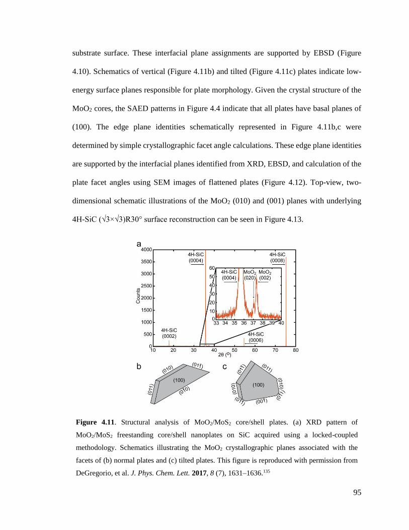
95
substrate surface. These interfacial plane assignments are supported by EBSD (Figure
4.10). Schematics of vertical (Figure 4.11b) and tilted (Figure 4.11c) plates indicate low-
energy surface planes responsible for plate morphology. Given the crystal structure of the
MoO2 cores, the SAED patterns in Figure 4.4 indicate that all plates have basal planes of
(100). The edge plane identities schematically represented in Figure 4.11b,c were
determined by simple crystallographic facet angle calculations. These edge plane identities
are supported by the interfacial planes identified from XRD, EBSD, and calculation of the
plate facet angles using SEM images of flattened plates (Figure 4.12). Top-view, two-
dimensional schematic illustrations of the MoO2 (010) and (001) planes with underlying
4H-SiC (√3×√3)R30° surface reconstruction can be seen in Figure 4.13.
Figure 4.11. Structural analysis of MoO2/MoS2 core/shell plates. (a) XRD pattern of
MoO2/MoS2 freestanding core/shell nanoplates on SiC acquired using a locked-coupled
methodology. Schematics illustrating the MoO2 crystallographic planes associated with the
facets of (b) normal plates and (c) tilted plates. This figure is reproduced with permission from
DeGregorio, et al. J. Phys. Chem. Lett. 2017, 8 (7), 1631–1636.135

96
Figure 4.12. SEM images of MoO2/MoS2 core-shell plates that have been pushed flat using
another bare SiC substrate. Higher-magnification SEM images of (b) tilted plates and (c) vertical
plates are labeled with average plate facet angle measurements. This figure is reproduced with
permission from DeGregorio, et al. J. Phys. Chem. Lett. 2017, 8 (7), 1631–1636.135
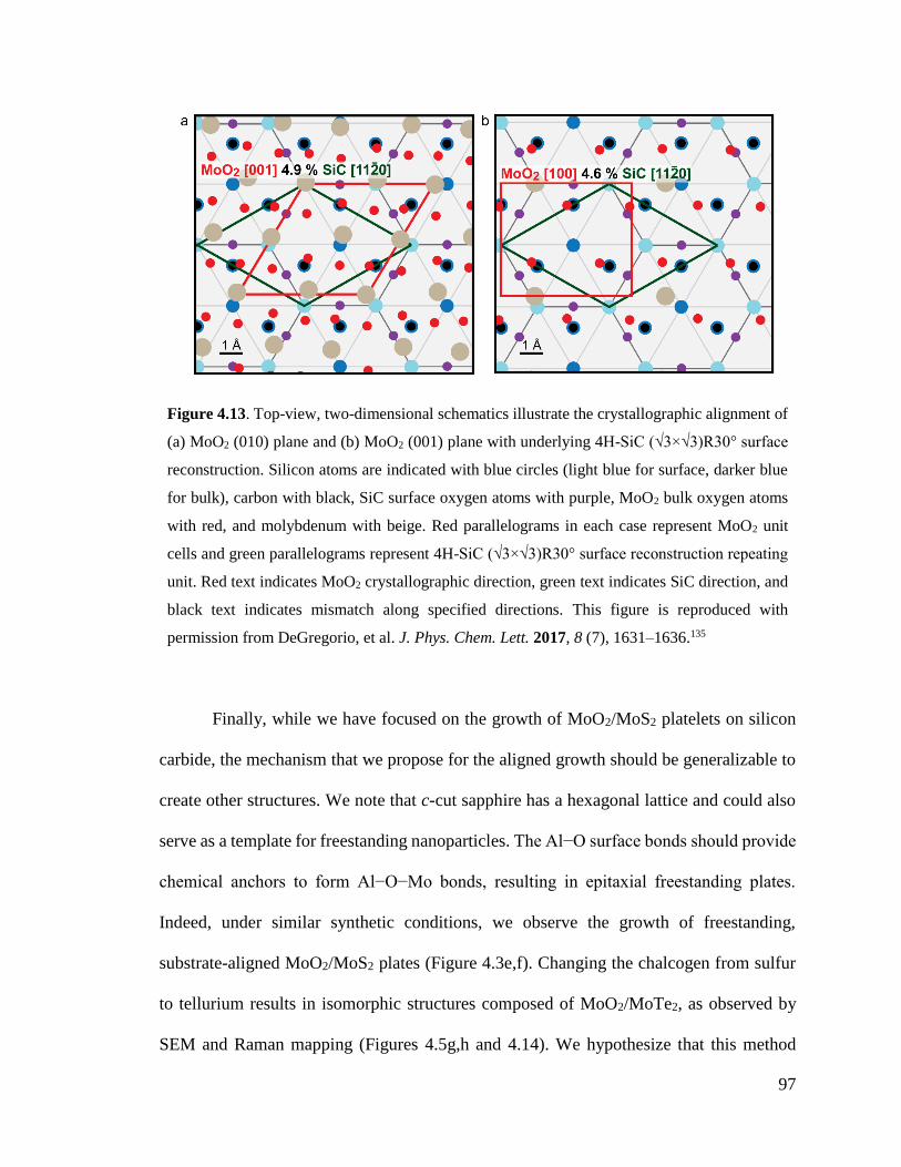
97
Figure 4.13. Top-view, two-dimensional schematics illustrate the crystallographic alignment of
(a) MoO2 (010) plane and (b) MoO2 (001) plane with underlying 4H-SiC (√3×√3)R30° surface
reconstruction. Silicon atoms are indicated with blue circles (light blue for surface, darker blue
for bulk), carbon with black, SiC surface oxygen atoms with purple, MoO2 bulk oxygen atoms
with red, and molybdenum with beige. Red parallelograms in each case represent MoO2 unit
cells and green parallelograms represent 4H-SiC (√3×√3)R30° surface reconstruction repeating
unit. Red text indicates MoO2 crystallographic direction, green text indicates SiC direction, and
black text indicates mismatch along specified directions. This figure is reproduced with
permission from DeGregorio, et al. J. Phys. Chem. Lett. 2017, 8 (7), 1631–1636.135
Finally, while we have focused on the growth of MoO2/MoS2 platelets on silicon
carbide, the mechanism that we propose for the aligned growth should be generalizable to
create other structures. We note that c-cut sapphire has a hexagonal lattice and could also
serve as a template for freestanding nanoparticles. The Al−O surface bonds should provide
chemical anchors to form Al−O−Mo bonds, resulting in epitaxial freestanding plates.
Indeed, under similar synthetic conditions, we observe the growth of freestanding,
substrate-aligned MoO2/MoS2 plates (Figure 4.3e,f). Changing the chalcogen from sulfur
to tellurium results in isomorphic structures composed of MoO2/MoTe2, as observed by
SEM and Raman mapping (Figures 4.5g,h and 4.14). We hypothesize that this method

98
could be extended to any single-crystal substrate that has suitable symmetry, size, and
chemical anchors to epitaxially nucleate the transition metal oxide. Furthermore, we
propose that future experiments could change the symmetry of the substrate to favor a
different interfacial plane of the MoO2 core, creating a pathway to form TMDC
nanoparticles with a wide variety of shapes and sizes.
Figure 4.14. Optical image and Raman maps of MoO2/MoTe2 core-shell plate. (a) Optical image
of a MoO2/MoTe2 core-shell plate. (b) Raman map of MoTe2 170 cm-1 mode of the MoO2/MoTe2
core-shell plate. (c) Raman map of MoO2 747 cm-1 mode of the MoO2/MoTe2 core-shell plate.
All scale bars are 2 μm. This figure is reproduced with permission from DeGregorio, et al. J.
Phys. Chem. Lett. 2017, 8 (7), 1631–1636.135
4.5 Conclusion
We have reported the novel growth of epitaxial, freestanding TMO/TMDC
core/shell nanoplates. These core/shell plates were initially grown as MoO2/MoS2
core/shell plates on 4H-SiC, but they are also shown to grow on other substrates, in the
case of MoO2/MoS2 plates grown on c-cut sapphire, and with other chalcogens, in the case
of MoO2/MoTe2 core/shell plates on c-cut sapphire. The growth mechanism of these
core/shell nanoplates is an extension of an established mechanism regarding self-seeding

99
TMDC monolayer growth. By delaying the chalcogen flux in this established mechanism,
we can control the morphology of the TMO seed prior to chalcogenization. Delaying the
chalcogen flux allows for the epitaxial growth of TMO plates on the substrate prior to the
formation of the TMDC, but this modification could be extended to create TMO seeds of
a variety of morphologies.
The method described here may be used as a general method for growing TMDC
materials in a controlled, oriented manner and linking them to the substrate by a metallic
core. The metallic TMO core could lead to improved charge injection in these
heterostructures, due to the epitaxial, covalent bonding with the substrate. These
TMO/TMDC core/shell nanoplates show promise in the field of catalysis, which requires
high densities of active sites in good contact with a conductive substrate. The procedure
described above should also be general to substrates of a variety of crystal structures, and
as such, this scheme could allow for the growth of core/shell nanoplates grown in many
epitaxial orientations. Finally, this modified mechanism offers pathways for creating new
families of TMDC and TMO/TMDC nanoparticles controlled by substrate surface
chemistry for future study.

100
Chapter 5
Metal-Semiconductor Heterostructures
101
5.1 Preface
Metal-semiconductor heterostructures are extremely important to consider in the
context of electronics applications of TMDCs. Given that noble metals form contacts with
high contact resistance, novel metal-semiconductor heterostructures must be investigated.
Two different TMDC metal-semiconductor systems are investigated here.
First is the fabrication of in-plane 2H-1T´ MoTe2 homojunctions by the flux-
controlled, phase engineering of few-layer MoTe2 from Mo nanoislands. The phase of few-
layer MoTe2 in this system is controlled by changing the Te atomic flux controlled by the
temperature of the reaction vessel. Few-layer 2H MoTe2 is formed with high Te flux, few-
layer 1T´ MoTe2 is formed with low Te flux, and few-layer in-plane 2H-1T´ MoTe2
homojunctions are formed with moderate Te flux. KPFM and Raman mapping confirm
that in-plane 2H-1T´ MoTe2 homojunctions have abrupt interfaces between the two
material domains, and they possess a potential difference of approximately 100 mV. This
method is extended to a two-step lithographic process to create patterned junctions between
2H and 1T´ MoTe2. FETs of these in-plane 2H-1T´ MoTe2 homojunctions were
subsequently fabricated, and the use of 1T´ MoTe2 as metallic electrodes in the FETs
improves device performance by decreasing the contact resistance. The contact resistance
extracted from transfer length method measurements is 470 ± 300 Ω-µm. Temperature-
dependent transport characteristic measurements indicate a barrier height at the lateral 2H-
1T´ interface on the order of 10 meV, several times smaller than the metal-2H Schottky
barrier height.
Secondly, lateral heterostructures between ML WS2 and few-layer NbS2 films are
demonstrated here. These WS2/NbS2 heterostructures show abrupt edges between the two
102
materials, as indicated by SEM, Raman, AFM, KPFM, and PL mapping. FETs were also
fabricated using these lateral WS2/NbS2 heterostructures. Preliminary device performance
shows that the NbS2 films are indeed metallic and show promise as a 2D TMDC contact
material. However, due to device fabrication limitations related to sample degradation and
resist under-exposure, the true electronic properties of WS2/NbS2 heterostructures have yet
to be determined.
5.2 Introduction
5.2.1 Metal-Semiconductor Heterostructures
Metal-semiconductor heterostructures, as the name implies, describe the interface
between a metal and a semiconductor. These heterostructures are typically designed with
the intent of forming a FET or other electronic device that would use the semiconducting
material as the channel and the metals on either side as contacts. When a semiconductor
comes into contact with a metal, a barrier layer forms at the interface.70 Charge carriers
become depleted in this region, and thus it is referred to as the depletion region. Depending
on the alignment of the metal’s work function and the semiconductor’s VB maximum and
CB minimum, this depletion region can result in ohmic contact, in which charge can flow
easily between both materials, or a Schottky barrier, in which the charge depletion induces
a barrier that impedes the flow of charge.47
Some of the most common electronic devices are based on bulk 3D channels
comprised of silicon or III−V semiconductors, such as GaAs or GaN, connected by noble
metal contacts, such as Au, Ag, or Pt.149 Bulk devices have been developed to exhibit ideal
device properties, including ohmic contacts, large on-off ratios, and good charge transfer

103
efficiency.150–152 Generally, such devices can be cost-effective and have been scalable
down to nanoscale dimensions. However, as devices are continually pushed to smaller
geometries, many of these traditional 3D devices struggle with fundamental limitations,
including poor heat dissipation, high leakage currents, and tunneling effects.153–155 2D
materials, by nature of their sub-nanometer layer thickness and unique electronic
properties, show promise for improved device properties in the small size limit.20
5.2.2 Device Considerations for 2D Materials
Using traditional metal contacts for 2D semiconductor devices has been shown to
induce a large contact resistance between the metal contact and 2D semiconductor.156 The
nature of this interface is very important, because a large contact resistance fundamentally
limits the drain current and charge transfer efficiency of the device. The large contact
resistance in 2D devices typically arises from the poor adhesion and general lack of
chemical bonding that occurs between the deposited noble metal and 2D material due to
the van der Waals forces at the 2D material surface. This contrasts with a bulk
semiconductor device, in which covalent bonds can more easily form between the
deposited metal and a reactive surface of a 3D semiconductor. The layered, van der Waals
nature of all 2D materials generally prevents the possibility of binding with top-down
deposited metals, giving rise to a tunneling barrier between the metal and the
semiconductor in many 2D material devices.
One promising strategy for overcoming high-contact-resistance junctions with 2D
semiconductors is to create lateral edge contacts.156 2D materials are more reactive at their
edge sites, thus stronger chemical bonds more likely to form at the edges of a 2D material.

104
Modeling has shown that edge contacts lead to shorter bonding distances, stronger
hybridization, and reduced overall contact resistance.156–159 These effects are especially
pronounced in the case of 2D materials due to the large conductivity anisotropy between
the in- and out-of-plane directions in 2D materials. It is also worth considering the choice
of metal, as this can affect the overall contact resistance. While noble metals can be used
to form edge contacts, it is difficult to control the precise contact position with traditional
metal deposition, and thus it is difficult to control the charge injection pathway in the
device. Metallic 2D materials can also be used, which can allow for native chemical
bonding and fewer dangling bonds at the lateral interface. The efforts I have made to create
metallic 2D TMDC contacts to semiconducting 2D TMDCs will be detailed in the
remainder of this chapter.
5.2.3 In-Plane 2H-1T´ MoTe2 Homojunctions
The electronic properties of TMDCs are enriched by their polymorphism, with
varying stacking orders and coordination geometry around the metal center that change the
material properties.2,4,33,160 Traditionally, and most notably true for Mo- and W-based
TMDCs, the 2H phase is semiconducting and features trigonal prismatic coordination,
whereas the 1T phase is metallic and has octahedral coordination. Despite these enticing
and disparate properties, tailoring the electronic properties of TMDCs is challenging,
because of the metastability of 1T TMDCs and the large free energy difference between
2H and 1T TMDCs.161–163
MoTe2 is an exciting candidate material due to its large spin-orbit coupling and the
fact that the 2H phase possesses a narrow band gap of 0.9−1.1 eV (notably similar to that

105
of Si, 1.1 eV).164–167 These properties make MoTe2 an ideal candidate for spintronic
devices, valleytronic devices, and optoelectronic devices operating in the near-infrared
frequency range. One of the chief features of MoTe2 is its phase tunability, originating from
a relatively small free energy difference (40 meV per unit cell) between the 2H and 1T´
phases of MoTe2.162,168,169 Semiconducting 2H MoTe2 is the most thermodynamically
favorable phase, but semimetallic 1T´ MoTe2 (1T MoTe2 that has undergone a Peierls
distortion) can also be favored under specific conditions.141,170 2H MoTe2 has been reported
to transform into 1T´ MoTe2 under applied tensile strain or by inducing Te deficiencies
through laser illumination.168,169 If one could control the phase of MoTe2 by simply
controlling the reaction conditions, phase-patterned MoTe2 could be mass produced for
device fabrication.
Electronic and optoelectronic applications of 2D TMDCs require
semiconductor−semiconductor junctions to allow for device functionality (e.g., p−n
junctions, diodes, and FETs) and metal−semiconductor contacts to inject charges. As was
discussed in Chapter 3, in-plane semiconducting TMDC heterostructures have been
previously synthesized, and these heterostructures possess an abrupt change in electronic
and optical properties across the atomically sharp junctions.76,83,84,101 Edge contacts have
been formed in 2D material-based metal−semiconductor junctions to increase transistor
“on” currents and effective charge mobility, as compared to traditional metal contacts.156,171
When the metal and semiconducting materials are two phases of the same material, the
barrier to charge injection can be quite low, thereby resulting in ideal, minimally resistive,
Ohmic contacts.161,168 Metal−semiconductor homojunctions in MoTe2 have previously
been fabricated via applied strain or laser illumination, but prior to this report, no group

106
has reported a direct synthetic approach for creating important metal−semiconductor
homojunctions in any 2D material.
Here we report the fabrication of in-plane 2H-1T´ MoTe2 homojunctions using
flux-controlled phase engineering of few-layer MoTe2 from Mo nanoisland precursors. The
phase of few-layer MoTe2 is controlled by changing the Te atomic flux through the reaction
vessel temperature. At high Te flux conditions, few-layer 2H MoTe2 is formed, whereas
few-layer 1T´ MoTe2 is obtained with low Te flux. Few-layer, in-plane 2H-1T´ MoTe2
homojunctions are synthesized using an intermediate Te flux condition. 2H-1T´ MoTe2
homojunctions are confirmed to have abrupt interfaces between the 2H and 1T´ domains
by Kelvin probe force microscopy (KPFM) and Raman mapping, with an approximately
100 mV potential difference between the domains. Furthermore, patterned few-layer 2H-
1T´ MoTe2 heterostructures are fabricated using a phase-selective synthetic strategy. This
flux-controlled phase engineering method could be utilized for the large-scale controlled
fabrication of 2D metal−semiconductor junctions for future electronic and optoelectronic
devices. This work is reproduced with permission from Yoo, et al.172
5.2.4 2H-1T´ MoTe2 Devices
The in-plane 2H-1T´ MoTe2 homojunctions discussed in the previous section were
used to fabricate in-plane field-effect transistors (FETs) to assess their electronic
properties. As was discussed in Chapter 1, semiconducting TMDCs frequently have
tunable bandgaps and ambipolar transport behavior, which makes them well-suited for use
in CMOS logic circuits. Moreover, no devices with 1T´ have been published yet using as-
grown MoTe2, and the detailed electrical properties of as-grown 2H-1T´ MoTe2 interfaces

107
have not yet been studied. This section on the fabrication and measurement of 2H-1T´
MoTe2 homojunction devices is presented as a summary of the work performed in
collaboration with the Koester group at the University of Minnesota. The bulk of this work
was performed by Rui Ma.
5.2.5 WS2/NbS2 Heterostructures
Interfacing semiconducting 2D TMDCs with other 2D materials has given rise to
heterostructures of a wide range of properties. Increased control of growth conditions and
sample preparation with 2D TMDCs has allowed for the design of increasingly complex
2D heterostructures and device geometries in recent years.78,171,173,174 However, many
electronic devices featuring 2D materials suffer from large contact resistances at the metal
contact interface, as was discussed earlier in this chapter.156 Thus, it is imperative that the
contact resistance be minimized to allow for accurate property measurement and optimal
device performance.
One way to minimize the contact resistance of such a device is to form lateral
heterostructures using a metallic 2D TMDC. In a lateral heterostructure, covalent bonds
can form at the edge of the semiconducting TMDC layers, avoiding the involvement of the
van der Waals surface in the device geometry. Some recently published works have utilized
this strategy.161,175,176 Despite progress in this area, metal-semiconductor heterostructures
have not yet been achieved using NbS2, a metallic TMDC with a P63mc crystal structure.
NbS2 and WS2 both have the same crystal structure and similar lattice constants (aNbS2 =
3.33 Å, aWS2 = 3.16 Å),177 which should allow for favorable covalent bonding at the
interface with minimal strain and few dangling bonds.

108
In this work, CVD-grown, monolayer WS2 is used as a seed to grow few-layer NbS2
in a lateral WS2/NbS2 heterostructure geometry. In this heterostructure, metallic NbS2
functions as a 2D electrical contact to the semiconducting WS2. These heterostructures
were subsequently characterized, and electrical devices were made to determine the
electronic effects of using NbS2 as a contact material.
5.3 Experimental
5.3.1 In-Plane 2H-1T´ MoTe2 Homojunctions
In-plane 2H-1T´ MoTe2 homojunctions were synthesized from Mo nanoislands
using a horizontal hot-wall tube furnace equipped with mass flow controllers and a vacuum
pump, the same general setup as described above for MoS2 growth. Mo nanoislands were
deposited on SiO2/Si substrates using an e-beam evaporation setup at the Minnesota Nano
Center. Contact-mode AFM images and height line profiles show that the Mo nanoislands
have heights of about 1−3 nm and widths of a few hundred nanometers (Figure 5.1),
showing similar morphology to that of conventional transition metal nanoislands deposited
by e-beam evaporation.178 Te lump precursor was prepared by annealing Te slugs (0.8 g,
99.999%, Sigma Aldrich) at 635 ºC for one hour under an Ar environment. Mo nanoislands
on SiO2/Si were placed face-down on an alumina boat containing the Te lump precursor
placed at the center of the heating zone in a 3-inch quartz tube (MTI Corp.). After
evacuating the quartz tube to less than 100 mTorr, Ar gas was flowed at a rate of 500 sccm
until atmospheric pressure was reached. Ar and H2 were then each flowed at a rate of 5
sccm. During the reaction, the furnace was ramped to 585 ºC in 15 minutes and was kept

109
at this temperature for an hour. After the reaction, the furnace lid was opened so that the
furnace would cool rapidly to room temperature.
Figure 5.1. AFM of Mo nanoislands and in-plane 2H-1T′ homojunctions. (a) AFM height image
of Mo nanoislands deposited on SiO2/Si substrates. (b) AFM height image of in-plane 2H-1T′
homojunctions. (c) Height line profile along the dotted white line in (a). (d) Height line profile
along the dotted white line in (b). This figure is reproduced with permission from Yoo, et al.
Adv. Mater. 2017, 29 (16), 1605461.172
In-plane 2H-1T´ MoTe2 homojunction films are synthesized at a peak temperature
of 585 ºC, but this same procedure can be used to grow uniform films of few layer 2H
MoTe2 or 1T´ MoTe2 by simply changing the temperature of the reaction. 2H MoTe2 is
synthesized at 635 ºC, whereas 1T´ is synthesized at 535 ºC. Given that the reaction times
are the same in each of these cases, the linear ramp rate in each case was slightly different:
∼41 ºC/min for 2H MoTe2, ∼37 ºC/min for in-plane 2H-1T´ homojunctions, and
∼34 ºC/min for 1T´ MoTe2 films.

110
Using a phase selective synthetic strategy, we also demonstrate the patterning of
few-layer 2H-1T´ junctions. The fabrication process is illustrated in Figure 5.2. First, few-
layer 1T′ MoTe2 is synthesized from Mo nanoislands with low Te flux. These few-layer
1T′ MoTe2 samples were subsequently spincoated with (methyl methacrylate) (PMMA)
(MW ~950000). We wrote patterns using a Vistec EBPG 5000+ system, developed the
PMMA in 1:3 MIBK:IPA, and rinsed the sample in IPA. Using the PMMA patterns as a
protecting mask, the unmasked few-layer 1T′ MoTe2 was etched away in 30% H2O2
aqueous solutions for 3 min, and Mo nanoislands were deposited on the sample through e-
beam evaporation. The PMMA was lifted off in acetone for 30 minutes to obtain patterned
regions of 1T′ MoTe2 and Mo nanoislands, which were subsequently annealed with high
flux to make few-layer 2H-1T′ MoTe2 patterns.
Figure 5.2. Schematic illustration of the fabrication procedure for few-layer 2H-1T′ MoTe2
patterns. This figure is reproduced with permission from Yoo, et al. Adv. Mater. 2017, 29 (16),
1605461.172

111
Contact-mode AFM measurements were performed on a Bruker Nanoscope V
Multimode 8 SPM using silicon tips with nominal force constant of 0.60 N/m. KPFM
measurements were performed using a Bruker SCM-PIT probe possessing an electrically
conductive Pt-Ir coated tip with a tip radius of about 20 nm. Raman spectra and the maps
were acquired using a 632.8 nm laser excitation focused through a 100x objective lens with
a power of 30 μW at room temperature. SEM images were taken on a JEOL JSM-6500F
SEM operated at an accelerating voltage of 5 kV. XRD measurements were performed on
a Bruker D8 Discover equipped with a 2D X-ray diffractometer using a Co Kα radiation
point source.
In this work, I acquired the AFM and KPFM data of the in-plane 2H-1T´ MoTe2
homojunctions. I also contributed intellectually to the realization of these experiments and
have since replicated their results. The synthesis of in-plane 2H-1T´ MoTe2 homojunctions
for this work and all other material characterization was performed by Youngdong Yoo.
5.2.2 2H-1T´ MoTe2 Devices
In-plane 2H-1T´ MoTe2 homojunction samples were patterned and etched into
rectangular bars of 2H, 1T´, and 1T´-2H-1T´ MoTe2 regions, upon which contacts of Ti/Au
(10 nm/80 nm) were patterned and deposited. These devices were used to assess the device
performance of MoTe2 devices with and without the use of conducting 1T´ MoTe2 as an
electrical contact.
This work is presented as a summary of work performed largely by Rui Ma in the
Koester group. In these experiments, I was responsible for certain portions of the in-plane

112
2H-1T´ MoTe2 homojunction synthesis, as well as the Raman mapping. Much of the
experimental design was performed by Rui Ma and Youngdong Yoo, and all of the device
performance measurement was performed by Rui Ma and collaborators in the Koester and
Low groups.
5.2.3 WS2/NbS2 Heterostructures
Ultraclean WS2 monolayers were synthesized using a procedure reported
previously.84 A Lindberg/Blue M hot-wall, single-zone tube furnace was equipped with
mass flow controllers and an Edwards RV8 vacuum pump. An alumina boat containing
500 mg of WO3 powder (99.998 %, Alfa Aesar) was placed at the center of the furnace in
a 2-inch diameter quartz tube. A c-cut sapphire substrate was placed polished-face-up on
an upside-down alumina boat, which was placed a few centimeters downstream from the
center of the furnace. Sulfur pieces (99.999 %, Alfa Aesar) were located in another alumina
boat upstream from the center of the furnace. After evacuating the tube to less than 10
mtorr, Ar gas at 400 sccm was used to purge the tube. The Ar flow rate was then reduced
to 60 sccm (standard cubic centimeters per minute) and H2 gas was introduced at 15 sccm,
maintaining a chamber pressure of 550 mtorr during the reaction. The furnace was heated
to 1050 ºC at a rate of 11 ºC/min and kept at 1050 ºC for 5 min. The temperatures of the
substrate and sulfur powder were measured to be approximately 940 ºC and 160 ºC,
respectively. The furnace was rapidly cooled after the reaction.
To synthesize WS2/NbS2 heterostructures, monolayer WS2 grown on c-cut sapphire
was used as a substrate for NbS2 film growth. The NbS2 film growth described here is very
similar to the chloride-based, few-layer NbS2 growth described in Chapter 2. WS2/sapphire

113
substrates were placed at the center of the furnace in a 2-inch quartz tube, while S pieces
and 100 mg NbCl5 powder were placed upstream from the center of the furnace. Prior to
loading, NbCl5 powder was kept in a sealed vial with an Ar-rich atmosphere. Ar gas was
introduced at 200 sccm prior to precursor loading and tube evacuation, to create an Ar-rich
environment and minimize ambient degradation of the NbCl5 powder during setup. After
evacuating the tube, Ar gas was used to purge the tube. Ar and H2 gas were then introduced
at rates of 60 and 5 sccm, respectively, and the reaction was carried out at low pressure
(∼400 mtorr). The center of the furnace was heated to approximately 1000 ºC at an average
rate of 11 ºC/min. After the S precursor remained molten for 7 min, the furnace was rapidly
cooled.
Raman spectra and optical images were acquired using a Raman microscopy setup
featuring 532 nm laser excitation aligned through a 100x objective lens with incident power
of approximately 200 µW. AFM data was acquired in tapping mode on a Bruker Nanoscope
V Multimode 8 SPM using Si tips with nominal force constant of 42 N/m. KPFM
measurements were performed using a Bruker SCM-PIT-V2 probe comprised of a Pt−Ir
tip with radius of approximately 20 nm. SEM images and EDS data were acquired using a
JEOL JSM-6500F SEM and TEM images were acquired using a FEI Tecnai G2 F30 TEM.
SEM, EDS, and TEM characterization was performed with the help of Nick Seaton and
Jason Myers in the Characterization Facility at the University of Minnesota.
To ascertain the effectiveness of the NbS2 as a contact material in these
heterostructures, we have patterned samples in a metal−semiconductor−metal device
geometry (NbS2−WS2−NbS2) using e-beam lithography, with isolated regions of
monolayer WS2 laterally connected only to regions of NbS2. Similar to the results presented

114
in Section 5.2.2, this work was done in collaboration with the Koester group, with the
device fabrication performed by Rui Ma. Ti/Au (10 nm/80 nm) electrodes were deposited
on top of the metallic NbS2 film regions to read out the electronic properties of the patterned
devices, and printed ion gels were deposited on top of the flakes to function as a top gate.
NbS2-only and WS2-only control devices were also fabricated, in which isolated regions of
each single material were used for depositing electrodes and top-gate ion gels. Aside from
the device work and the SEM, EDS, and TEM characterization, all synthesis and
characterization of these materials was performed by the author.
5.4 Results and Discussion
5.4.1 In-Plane 2H-1T´ MoTe2 Homojunctions
The MoTe2 films obtained from the Mo nanoisland tellurization method can be seen
in Figure 5.3. These MoTe2 films are continuous and possess root-mean-square (RMS)
roughness of about 0.88 nm, as determined by AFM, which is relatively smooth compared
to the the 0.5−1 nm roughness of the underlying SiO2/Si substrates. The thickness of these
films were measured to be about 3.5 nm, consistent with the thickness of five layers of
MoTe2 (see Figure 5.4).140,179

115
Figure 5.3. Growth of in-plane 2H-1T´ MoTe2 homojunctions from Mo nanoislands. (a)
Schematic illustration of the growth process. (b−d) Optical image of few-layer 2H, in plane 2H-
1T´, and 1T´ MoTe2 synthesized at 635, 585, and 535 ºC, respectively (e) Raman spectra acquired
at the points marked by 1-4 in (b−d). (f) High-resolution XPS spectra showing Mo 3d peaks of
few-layer 2H and 1T´ MoTe2. (g) High-resolution XPS spectra showing Te 3d peaks of few-
layer 2H and 1T´ MoTe2. The Mo 3d and Te 3d peaks of few-layer 1T´ MoTe2 are downshifted
by ∼0.6 eV and ∼1.1 eV, respectively, compared to those of few-layer 2H MoTe2. This figure is
reproduced with permission from Yoo, et al. Adv. Mater. 2017, 29 (16), 1605461.172

116
Figure 5.4. AFM of scratched in-plane 2H-1T′ MoTe2 films. (a) AFM height image of in-plane
2H-1T′ MoTe2 films with tweezer scratch. (b) Height line profile along the dotted white line in
(a). This figure is reproduced with permission from Yoo, et al. Adv. Mater. 2017, 29 (16),
1605461.172
Optical images of few-layer MoTe2 films show that the MoTe2 in each case is very
uniform, with large optical contrast between 1T´ and 2H MoTe2 domains. The change in
optical contrast between the 1T´ and 2H MoTe2 is due to the change in the visible
absorption spectrum of each phase.141,164 Raman spectra taken from different points of a
2H/1T´ homojunction show that each domain exhibits phase-specific characteristic Raman
peaks: the Bg (163.0 cm−1) and Ag (260.1 cm−1) modes for 1T´ MoTe2, and the A1g
(170.9 cm−1) and E2g (233.5 cm−1) modes for 2H MoTe2.164,180 The crystal structures of as-
synthesized few-layer 2H and 1T´ MoTe2 were confirmed by XRD (Figure 5.5).

117
Figure 5.5. XRD patterns of few-layer 2H (red) and 1T′ (black) MoTe2. The peaks of as
synthesized few-layer 2H and 1T′ MoTe2 are indexed to hexagonal 2H MoTe2 (JCPDS #73-
1650) and monoclinic 1T′ MoTe2 (JCPDS #71-2157), respectively. This figure is reproduced
with permission from Yoo, et al. Adv. Mater. 2017, 29 (16), 1605461.172
XPS measurements allowed for the analysis of the elemental composition and
chemical states of few-layer MoTe2. The presence of elemental Mo and Te are confirmed
in few-layer 2H and few-layer 1T´ films by the XPS survey spectrum. Also present in the
survey spectrum are adventitious C and O signal, which originate from atmospheric
transfer of the material. These signals were used to calibrate the electron binding energies.
The high-resolution XPS peaks for 2H MoTe2 were observed at 228.4 eV (Mo 3d5/2),
231.5 eV (Mo 3d3/2), 573.1 eV (Te 3d5/2), and 583.5 eV (Mo 3d3/2). The high-resolution
XPS peaks for 1T´ MoTe2 were observed at 227.8 eV (Mo 3d5/2), 230.9 eV (Mo 3d3/2),
572.0 eV (Te 3d5/2), and 582.4 eV (Mo 3d3/2). The XPS peaks for 1T´ MoTe2 are reportedly
downshifted by about 0.4−0.6 eV from the XPS peaks of 2H MoTe2.140,168,179 In our few-

118
layer 1T´ MoTe2, however, the Te 3d peaks are downshifted by ∼1.1 eV, whereas the Mo
3d peaks are downshifted by ∼0.6 eV. We attribute this additional downshifting of the Te
3d peaks to Te deficiency. Chalcogen deficiency in TMDCs reportedly decreases the
binding energy of the chalcogen while maintaining the same binding energy of the
transition metal,181 which is consistent with our XPS measurements (Figure 5.6). The
Te/Mo atomic ratios of the MoTe2 films were quantified by comparing the area ratio of Mo
3d-to-Te 3d peaks of 2H MoTe2 with that of 1T´ MoTe2. When the value of this Te/Mo
atomic ratio for 2H MoTe2 is normalized to 2.00, the Te/Mo atomic ratio of 1T´ MoTe2 is
calculated to be about 1.86.
Figure 5.6. XPS survey spectrum of few-layer 2H (red) and 1T′ (blue) MoTe2. This figure is
reproduced with permission from Yoo, et al. Adv. Mater. 2017, 29 (16), 1605461.172

119
Based on the Te deficiency present in these few-layer 1T´ MoTe2 films, we
hypothesize that the flux of Te during the growth determines the phase of MoTe2,
consistent with the previously reported crystal growth.141,182 The experiments presented in
Figure 5.3 conflate two variables: substrate temperature and Te flux. Figure 5.7 shows a
series of reactions performed to exclude the influence of substrate temperature on the
resulting films. In these experiments, the Te flux was controlled independently by keeping
the substrate temperature at 635 ºC and placing the Te lump at four different positions in
the growth tube: A (635 ºC), B (585 ºC), C (535 ºC), and D (485 ºC). The vapor pressure
of Te was calculated to be approximately 10.9, 4.5, 1.7, and 0.5 Torr for the 635, 585, 535,
and 485 ºC conditions, respectively.183 Flux, defined as the number of deposited atoms per
unit time and area, is proportional to the vapor pressure. To this end, the Te flux at 635 ºC
is estimated to be approximately 20 times greater than at 485 ºC. Stokes and anti-Stokes
Raman spectra show that sample A (Te temperature of 635 ºC) exhibits characteristic
Raman peaks of 2H MoTe2, while sample C (Te temperature of 535 ºC) shows
characteristic Raman peaks of 1T´ MoTe2. Sample B (Te temperature of 585 ºC) shows
Raman peaks corresponding to both 2H and 1T´ MoTe2, indicating that the sample is
composed of both 2H and 1T´ MoTe2. Sample D (Te temperature of 485 ºC) exhibits
shifted Raman peaks of 1T´ MoTe2, likely due to the severe Te deficiency present in the
sample as a result of the dramatically decreased Te flux. Additional Raman measurements
and Lorentzian fitting results are shown in Figure 5.8.

120
Figure 5.7. Flux-controlled phase engineering of few-layer MoTe2. (a) Schematic illustration of
the experimental setup for flux-controlled reactions and the temperature profiles of the furnace
heated to 635 C. Te lump was placed at positions of A (635 ºC), B (585 ºC), C (535 ºC), and D
(485 ºC) for the syntheses of few-layer 2H, mixed 2H-1T´, 1T´, and defective 1T´ MoTe2,
respectively. The temperature of Mo nanoislands on SiO2/Si substrates was kept at 635 ºC for all
experiments. (b) Stokes and anti-Stokes Raman spectra of few-layer 2H, mixed 2H-1T´, 1T´, and
defective 1T´ MoTe2 synthesized at Te temperatures of 634, 585, 535, and 485 ºC, respectively.
This figure is reproduced with permission from Yoo, et al. Adv. Mater. 2017, 29 (16), 1605461.172

121
Figure 5.8. Raman spectra and Lorentzian fitting results of few-layer 2H, mixed 2H-1T′, 1T′,
and defective 1T′ MoTe2. This figure is reproduced with permission from Yoo, et al. Adv. Mater.
2017, 29 (16), 1605461.172
This synthesis is assumed to be in thermodynamic control, given that the Mo
nanoislands are annealed in a Te environment for long enough that they can reach
thermodynamic equilibrium. This is further supported by the observation that the changes
in phase are driven by the Te chemical potential. Density functional theory (DFT)
calculations have previously predicted that 2H MoTe2 is the most thermodynamically
stable phase for stoichiometric MoTe2, whereas the 1T´ phase becomes more stable as the
Te vacancy concentration increases.168 Here, it is demonstrated experimentally that the
MoTe2 phase is determined thermodynamically by the Te vacancy concentration, and we
provide optimum quantitative values of vapor pressures for the growth of 2H, mixed 2H-
1T´, and 1T´ MoTe2.

122
The in-plane 2H-1T´ MoTe2 homojunctions are further characterized by Raman
mapping and KPFM (Figure 5.9). An optical image of the 2H-1T´ MoTe2 region used for
Raman mapping shows clear optical contrast between the 2H and 1T´ domains. Raman
spectra indicate that the inner, circular area is composed of 2H MoTe2, whereas the outer
region is composed of 1T´ MoTe2. Raman maps of the 2H MoTe2 E2g mode and the 1T´
MoTe2 Bg mode show that the junctions between the 2H and 1T´ MoTe2 domains are
abrupt. An AFM height image and corresponding height line profile show that no
significant height difference exists between the 2H and 1T´ regions. A KPFM image and
corresponding potential line profile confirm that a sharp 100 mV potential difference exists
between the 2H and 1T´ MoTe2 domains. KPFM measures the contact potential difference
(CPD) between the scanning probe tip and the material.184 CPDs measured on 2H and 1T´
MoTe2 are defined to be [Φ(tip) – Φ(2H MoTe2)]/e and [Φ(tip) – Φ(1T´ MoTe2)]/e, where
Φ(tip), Φ(2H MoTe2), and Φ(1T´ MoTe2) are the work functions for the tip, 2H MoTe2,
and 1T´ MoTe2, respectively. Based on the KPFM measurement, the work function
difference between the 2H and 1T´ MoTe2 domains, Φ(2H MoTe2) – Φ(1T´ MoTe2), is
calculated to be approximately 100 meV. This work function difference can be attributed
to the Te deficiency in 1T´ MoTe2 and the electronic structure difference between 2H and
1T´ MoTe2. An atomic model of in-plane 2H-1T´ MoTe2 junctions is illustrated in Figure
5.9i.
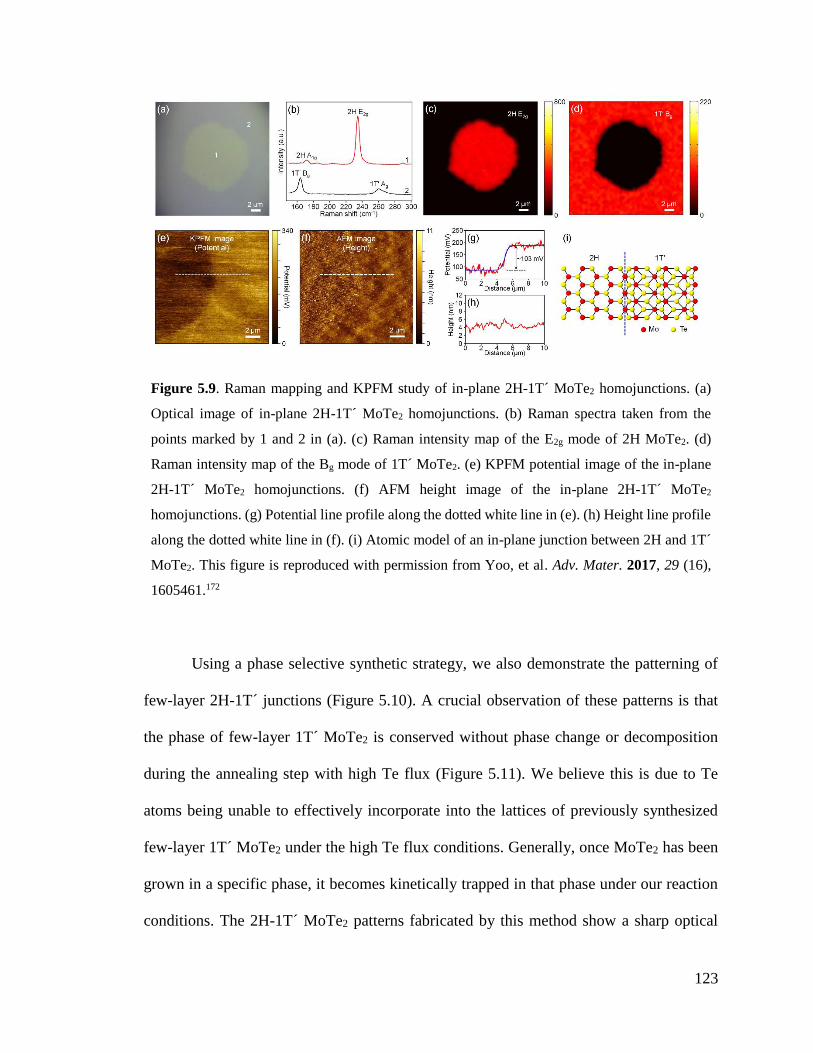
123
Figure 5.9. Raman mapping and KPFM study of in-plane 2H-1T´ MoTe2 homojunctions. (a)
Optical image of in-plane 2H-1T´ MoTe2 homojunctions. (b) Raman spectra taken from the
points marked by 1 and 2 in (a). (c) Raman intensity map of the E2g mode of 2H MoTe2. (d)
Raman intensity map of the Bg mode of 1T´ MoTe2. (e) KPFM potential image of the in-plane
2H-1T´ MoTe2 homojunctions. (f) AFM height image of the in-plane 2H-1T´ MoTe2
homojunctions. (g) Potential line profile along the dotted white line in (e). (h) Height line profile
along the dotted white line in (f). (i) Atomic model of an in-plane junction between 2H and 1T´
MoTe2. This figure is reproduced with permission from Yoo, et al. Adv. Mater. 2017, 29 (16),
1605461.172
Using a phase selective synthetic strategy, we also demonstrate the patterning of
few-layer 2H-1T´ junctions (Figure 5.10). A crucial observation of these patterns is that
the phase of few-layer 1T´ MoTe2 is conserved without phase change or decomposition
during the annealing step with high Te flux (Figure 5.11). We believe this is due to Te
atoms being unable to effectively incorporate into the lattices of previously synthesized
few-layer 1T´ MoTe2 under the high Te flux conditions. Generally, once MoTe2 has been
grown in a specific phase, it becomes kinetically trapped in that phase under our reaction
conditions. The 2H-1T´ MoTe2 patterns fabricated by this method show a sharp optical

124
contrast between the inner and outer regions. Raman measurements and mapping confirm
that the inner and outer domains of these patterned junctions are 2H and 1T´ MoTe2,
respectively, and that the junction features abrupt interfaces between the 2H and 1T´
domains.
Figure 5.10. Fabrication of few-layer 2H-1T´ MoTe2 patterns. (a) Optical image of 2H-1T´
MoTe2 patterns. (b) Raman spectra taken from the points marked by 1 and 2 in (a). (c) Raman
intensity map of the E2g mode of 2H MoTe2. (d) Raman intensity map of the Bg mode of 1T´
MoTe2. This figure is reproduced with permission from Yoo, et al. Adv. Mater. 2017, 29 (16),
1605461.172

125
Figure 5.11. Phase conservation of few-layer 1T′ MoTe2 during annealing with high Te flux.
Raman spectra of the 1T′ MoTe2 before (black) and after (red) annealing with high Te flux. This
figure is reproduced with permission from Yoo, et al. Adv. Mater. 2017, 29 (16), 1605461.172
5.4.2 2H-1T´ MoTe2 Devices
The in-plane 2H-1T´ MoTe2 homojunctions discussed in the previous section were
used to fabricate in-plane field-effect transistors (FETs) to assess their electronic
properties. Figure 5.12 shows an optical image and Raman peak intensity maps of
representative 1T´-2H-1T´ MoTe2 devices, showing optical contrast and Raman peak
intensity differences between the interior 2H and exterior 1T´ regions that indicate an
abrupt junction between the two phases.

126
Figure 5.12. Schematic illustration and Raman mapping of 1T´-2H-1T´ MoTe2 devices. (a)
Schematic diagram of an in-plane, monolayer 1T´-2H-1T´ MoTe2 homojunction. The top
schematic in (a) is a cross-section view and the bottom is a basal plane view, with blue spheres
representing Mo atoms, yellow spheres representing Te atoms, and the red dashed boxes
representing primitive unit cells. (b) Optical image of a few-layer 1T´-2H-1T´ MoTe2 device. (c)
Raman spectra acquired from the 1T´ and 2H regions in (b). (d) and (e) are Raman intensity maps
of the E2g mode of 2H MoTe2 and the Bg mode of 1T´ MoTe2, respectively, acquired from the
region indicated by the red dashed rectangle in (b). White dashed lines in (d) and (e) indicate the
borders of the Ti/Au contacts. This figure is reproduced with permission from Ma, et al.
Manuscript in preparation.
The transfer length method was used to determine the contact resistances of 1T´-
only and 2H-only devices (Figure 5.13). The contact resistance between Ti/Au and 1T´
MoTe2 was determined to be 0.47 ± 0.03 kΩ-µm and the sheet resistance of the 1T´ MoTe2
was determined to be 2.65 ± 0.09 kΩ-µm with no applied backgate voltage (VBG), which
are comparable to the lowest published resistance values for phase-transitioned FETs of
TMDCs (200–300 Ω-µm).161 The contact resistance between Ti/Au and 2H MoTe2 was
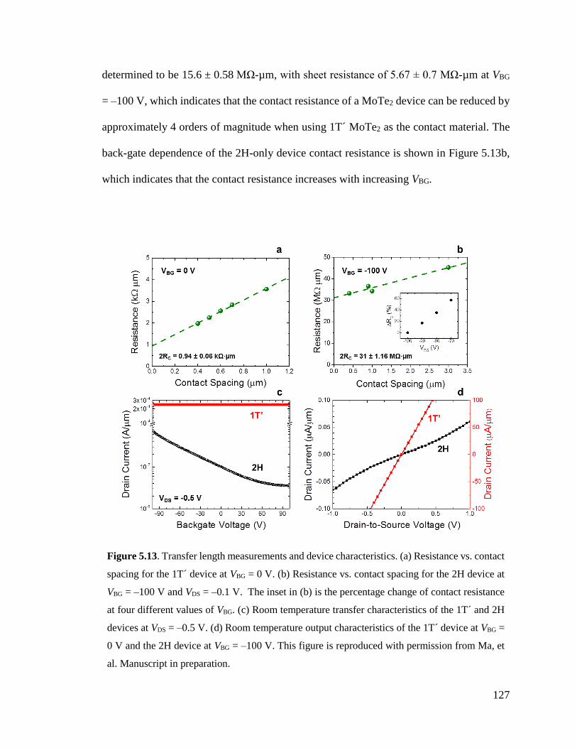
127
determined to be 15.6 ± 0.58 MΩ-µm, with sheet resistance of 5.67 ± 0.7 MΩ-µm at VBG
= –100 V, which indicates that the contact resistance of a MoTe2 device can be reduced by
approximately 4 orders of magnitude when using 1T´ MoTe2 as the contact material. The
back-gate dependence of the 2H-only device contact resistance is shown in Figure 5.13b,
which indicates that the contact resistance increases with increasing VBG.
Figure 5.13. Transfer length measurements and device characteristics. (a) Resistance vs. contact
spacing for the 1T´ device at VBG = 0 V. (b) Resistance vs. contact spacing for the 2H device at
VBG = –100 V and VDS = –0.1 V. The inset in (b) is the percentage change of contact resistance
at four different values of VBG. (c) Room temperature transfer characteristics of the 1T´ and 2H
devices at VDS = –0.5 V. (d) Room temperature output characteristics of the 1T´ device at VBG =
0 V and the 2H device at VBG = –100 V. This figure is reproduced with permission from Ma, et
al. Manuscript in preparation.

128
Room-temperature transfer characteristics of drain current (ID) vs. VBG of 1T´-only
and 2H-only devices (Figure 5.13c) indicate that the 1T´-only device shows high drive
current (245 µA/µm at VDS = –0.5 V) and no gate modulation, thereby confirming its
metallicity. The 2H-only device shows typical metal-oxide-semiconductor field-effect
transistor (MOSFET) transfer characteristic with a current on/off ratio of ∼103, possibly
affected by defects in the channel. The interface trap density of this device is calculated to
be ∼1013 cm-2/eV at room temperature. The room-temperature output characteristics (ID vs.
VDS) of the 1T´-only device (Figure 5.13d) show that the current of the 1T´-only device is
more than 4 orders of magnitude larger than that of the 2H-only device at the same VDS.
Additionally, the 1T´-only device shows a linear relationship whereas the 2H-only device
shows nonlinear behavior, supporting the assignment of 1T´ and 2H MoTe2 as metallic and
semiconducting, respectively.
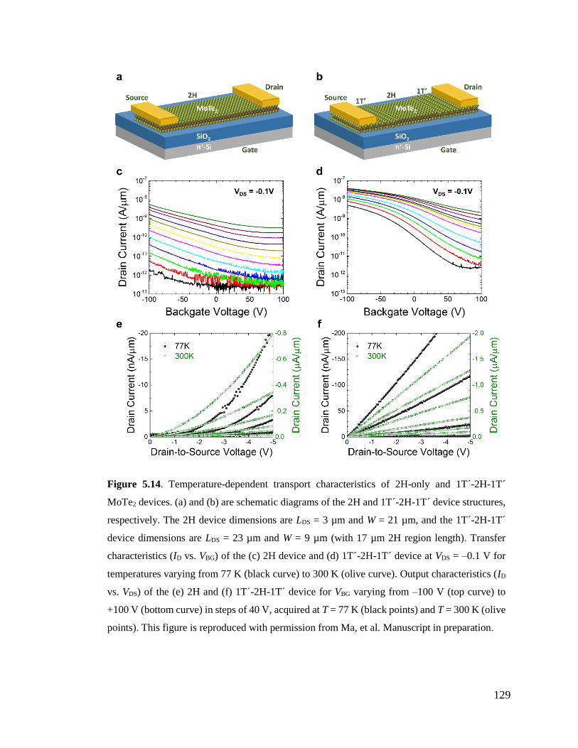
129
Figure 5.14. Temperature-dependent transport characteristics of 2H-only and 1T´-2H-1T´
MoTe2 devices. (a) and (b) are schematic diagrams of the 2H and 1T´-2H-1T´ device structures,
respectively. The 2H device dimensions are LDS = 3 µm and W = 21 µm, and the 1T´-2H-1T´
device dimensions are LDS = 23 µm and W = 9 µm (with 17 µm 2H region length). Transfer
characteristics (ID vs. VBG) of the (c) 2H device and (d) 1T´-2H-1T´ device at VDS = –0.1 V for
temperatures varying from 77 K (black curve) to 300 K (olive curve). Output characteristics (ID
vs. VDS) of the (e) 2H and (f) 1T´-2H-1T´ device for VBG varying from –100 V (top curve) to
+100 V (bottom curve) in steps of 40 V, acquired at T = 77 K (black points) and T = 300 K (olive
points). This figure is reproduced with permission from Ma, et al. Manuscript in preparation.

130
The temperature-dependent device behavior for 2H-only and 1T´/2H/1T´ device
geometries (Figure 5.14) show that the on-current, current on/off ratio, and subthreshold
swing (SS) are all improved by the use of 1T´ electrodes. The on-current, current on/off
ratio, and SS for the 1T´/2H/1T´ device all increase with decreasing temperature,
suggesting that the current of the 1T´/2H/1T´ device is in the mobility-limited regime, as
opposed to the thermionic-limited regime. Improvement of the current on/off ratio and SS
is not strongly observed in the 2H-only device, indicating that the current is limited by
thermionic transport associated with the metal/MoTe2 interface in this case. Table 5.1
compares the performance of the 2H-only and 1T´/2H/1T´ devices, and is reproduced with
permission from Ma, et al. (manuscript in preparation). Each of the properties compared in
Table 5.1 shows a significant improvement with the 1T´/2H/1T´ devices. It is important to
note that these devices have relatively high defect density, suggesting the need for further
work to reduce the defects in the as-grown MoTe2.
The hole mobility was extracted from the temperature-dependent transfer
characteristics for 2H-only and 1T′/2H/1T′ devices. The hole mobility at a given
temperature and VDS is extracted at the maximum transconductance, gm, which is the
maximum derivative of the ID-VGS curve. The hole mobility, µ, is then calculated by
𝜇 = 𝑔𝑚∙𝐿
𝑊∙𝐶𝑜𝑥∙𝑉𝐷𝑆 (4.1)
where L and W are the length and width of the device, respectively, Cox is the gate dielectric
capacitance, and VDS is the drain-to-source voltage. The extracted hole mobility as a
function of temperature for the 2H-only and the 1T′/2H/1T′ devices are shown in Figure
5.15.

131
Figure 5.15. Hole mobility (log scale) as a function of temperature (log scale) for the (a) 2H-
only device and the (b) 1T′/2H/1T′ device in Figure 5.14 at different values of VDS. This figure
is reproduced with permission from Ma, et al. Manuscript in preparation.
The 1T′/2H/1T′ device shows more than 10 times higher hole mobility than that of
the 2H-only device, which is a logical result of the reduced contact resistances at the
metal/1T′ and 1T′/2H interfaces. The mobility is relatively low in both devices because of
the high defect density in the as-grown MoTe2. The 2H-only and 1T′/2H/1T′ devices show
a power-law mobility vs. temperature dependence, µ Tx, where x = 5.9 and x = 1.3,
respectively. The slope of the 1T′/2H/1T′ device is close to the typical factor of x = 1.5 for
impurity scattering-dominant transport in the material due to the negligible effect of the
contacts. This confirms the ohmic nature of the metal/1T′ and 1T′/2H interfaces.
Additionally, the dependence of VDS on the hole mobility in the 1T′/2H/1T′ device is less
than that in the 2H-only device, again confirming ohmic contacts in the 1T′/2H/1T′ device.
For the 2H-only device, the contact resistance and sheet resistance are of the same order of
magnitude, thus one would expect higher VDS dependence.

132
Table 5.1. Comparison of 2H and 1T´-2H-1T´ device performance.
Improvement in the contact resistance when using the metal/1T´ electrode design
is also observed in the output characteristics (ID vs. VDS) of the devices shown in Figures
5.14e–f. The linear output characteristics of the 1T´/2H/1T´ device at 300 and 77 K
indicates ohmic behavior of the 1T´ electrode and the 1T´/2H interface, whereas the output
characteristics of the 2H device are nonlinear and become severe at low temperature,
suggesting the presence of a Schottky barrier at the metal-2H interface.
Temperature-dependent transfer characteristics were used to extract Schottky
barrier heights for three interfaces: (1) Metal/2H MoTe2, (2) metal/1T´ MoTe2, and (3)
1T´/2H MoTe2. The thermionic emission equation was used to model the temperature and
bias dependence of ID, expressed as
𝐼𝐷 = 𝐴∗∗𝑇1.5exp [−1
𝑘𝐵𝑇(Φ𝑆𝐵) −
𝑞𝑉𝐷𝑆
𝜂] (4.2)
where A** is the effective Richardson constant, T is the temperature, kB is the Boltzmann
constant, ΦSB is the Schottky barrier height between the metal Fermi energy and the valence
band edge of 2H MoTe2, q is the electronic charge, VDS is the drain-to-source voltage, and
η is the ideality factor. The activation energy is denoted by (ΦSB – qVDS/η), and ΦSB at each
133
gate voltage is extracted by the Arrhenius plot, ln(ID/T1.5) vs. 1/kBT, at different values of
VDS.
The Arrhenius plots for a 1T´-only device at VBG = 0 V (Figure 5.16a) show positive
slope values, indicating a negative activation energy. This suggests that the conductivity of
1T´ MoTe2 decreases with increasing temperature, thereby implying that 1T´ MoTe2 is
metallic or semi-metallic. The Arrhenius plots for a 2H-only device at VBG = –100 V
(Figure 5.16b) show negative slope values, indicating thermally-activated transport.
Similar behavior was observed for all VBG values used. Finally, the Arrhenius plots for a
1T´/2H/1T´ device at VBG = –100 V (Figure 5.16c) also show negative slope values,
indicating thermally-activated transport. However, since no thermally-activated transport
was observed for the metal/1T´ interface, the energy barrier associated with transport in
the 1T´/2H/1T´ device must be associated with the 1T´/2H interface and not the metal/1T´
interface.

134
Figure 5.16. Arrhenius plots and bias-dependent effective barrier heights. (a) Arrhenius plots of
ln(ID/T1.5) vs. 1/kBT for the 1T´-only device (depicted above the (a) panel) at VBG = 0 V for
different values of VDS. The positive slopes here indicate the absence of an energy barrier at the
metal/1T´ interface. (b) Arrhenius plots for the 2H-only device at VBG = –100 V for different
values of VDS. (c) Arrhenius plots for the 1T´/2H/1T´ device at VBG = –100 V for different values
of VDS. Given the absence of a barrier at the metal/1T´ interface, the positive slope in (c) is an
indication of the barrier height at the 1T´/2H interface. This figure is reproduced with permission
from Ma, et al. Manuscript in preparation.
According to Equation 4.2, the Arrhenius curve slopes can be plotted as a function
of VDS and then extrapolated to VDS = 0 V to extract the effective hole Schottky barrier
height, ΦSB. The slopes of the Arrhenius curves are (qVDS/η – ΦSB), so the effective
Schottky barrier height, ΦSB, can be extracted by plotting the slopes vs. VDS and then
extrapolating to VDS = 0 V. A representative plot of the extraction for a 2H-only device at
a given VBG is shown in Figure 5.17. ΦSB is extracted for all values of VBG. The results of
this extrapolation for the 2H-only device and the 1T´/2H/1T´ device (Figure 5.18) show
that the overall barrier height for the 1T´/2H/1T´ device is significantly lower than that of
the 2H-only device over the entire range of VBG.

135
Figure 5.17. Plot of the slopes of the Arrhenius plot for the 2H-only device in Figure 5.14 vs.
VDS at VBG = –100 V. This figure is reproduced with permission from Ma, et al. Manuscript in
preparation.
Figure 5.18. Effective Schottky barrier height of the 2H device (black curve) and the 1T´/2H/1T´
device (red curve) as a function of VBG. Error bars are extracted from the fitting shown in Figure
5.16. This figure is reproduced with permission from Ma, et al. Manuscript in preparation.

136
These results are qualitatively consistent with the Schottky barrier heights extracted
for metal contacts to exfoliated 2H MoTe2,185,186 and the 1T´/2H energy barrier is also
consistent with that previously observed for exfoliated MoTe2 with process-induced 1T´
regions.168 However, some discrepancy exists in the gate voltage dependence of the barrier
height for the metal/2H contacts. In a previous report,186 the effective barrier height was
found to have a strong gate voltage dependence, with the barrier height increasing to
300 meV near the transistor off-state to near 0 V in the strong on-state region.
Contrastingly, our work shows that the metal/2H barrier height has only a small gate
voltage dependence, with similar behavior for the 1T´/2H barrier height. This behavior is
likely due to the presence of defects in MoTe2, which can lead to trap-assisted tunneling of
carriers from the metal contacts into the MoTe2.
We have also performed density functional theory (DFT) calculations of monolayer
to five-layer 1T´ and 2H MoTe2 band structures to estimate the expected band alignments.
Figure 5.19 shows the computed band structures of 5-layer 2H and 5-layer 1T′ MoTe2.
Using PBE/GGA with spin-orbit coupling, the 5-layer 2H MoTe2 is determined to be a
semiconductor with an indirect band gap of 0.75 eV. This band gap is smaller than the
experimentally determined value, but DFT has long been shown to underestimate the
magnitude of band gaps. For the 5-layer 1T′ MoTe2, the band gap is closed and the CB
minimum and VB maximum are overlapping. Because these CB and VB states are not
completely separated, the 5-layer 1T′ MoTe2 is determined to be semi-metallic.

137
Figure 5.19. Calculated band structures of (a) 5-layer 2H MoTe2, and (b) 5-layer 1T′ MoTe2,
respectively, with spin-orbit coupling included. Inset are the crystallographic unit cells. This
figure is reproduced with permission from Ma, et al. Manuscript in preparation.
DFT calculations confirm that 1T´ and 2H MoTe2 are metallic and semiconducting,
respectively. DFT calculations also show that the Fermi level at the five-layer 1T´/2H
boundary is within ∼100 meV of the valence band edge, which is much closer than
expected for Ti contacts to 2H MoTe2.187 We believe that the effect of trap-assisted
transport in our samples makes it difficult to perform a truly quantitative comparison with
experimental data.
The thickness dependent band gap determined by the difference between the CB
minimum and VB maximum is shown in Figure 5.20a. The barrier heights (for holes) at
the 2H/1T′ interface were calculated using the Schottky-Mott model,188 which assumes that
the barrier for holes is the energy difference between the work function of the metal and
the VB maximum of the semiconductor. The calculated barrier heights as a function of
layer number are shown in Figure 5.20b.

138
Figure 5.20. (a) Band gap of 2H MoTe2 and (b) barrier height at the 2H/1T′ interface as a
function of layer number. This figure is reproduced with permission from Ma, et al. Manuscript
in preparation.
The calculated barrier height for the 5-layer 2H-1T′ interface is ∼136 meV. This is
much larger than the electrically determined value in Figure 5.18, but it has been previously
demonstrated that the Schottky-Mott model is insufficient in predicting the barrier height
of 2D lateral heterostructures.189 Sophisticated models are needed to more accurately
estimate the barrier heights, possibly including the construction a supercell that consists of
both material phases. Another possible explanation for this barrier height discrepancy is
that the interfacial traps in our devices may pin the Fermi level of 1T′ MoTe2 closer to the
VB of 2H MoTe2.
Finally, we note that the roll-off of the Schottky barrier for the 1T´/2H/1T´ device
in Figure 5.18 at positive gate voltages is unexpected, because the effective barrier height
should continue to increase to at least half of the band gap before decreasing due to the
onset of ambipolar transport.185 Thus, additional experiments and simulations are needed
to understand the role of traps and the electrostatic effects of the in-plane 1T´/2H
heterostructures.

139
5.4.3 WS2/NbS2 Heterostructures
WS2/NbS2 lateral heterostructures grown via CVD can be seen in Figure 5.21. The
as-grown WS2 triangular flakes grown on bare c-cut sapphire are shown in the
representative optical microscope image in Figure 5.21a and confirmed to be monolayer
by PL spectroscopy (Figure 5.21b), showing strong PL peak intensity.99 Subsequent NbS2
growth on these samples results in the lateral heterostructures visible in the optical image
in Figure 5.21c. Raman spectra (Figure 5.21d) confirm the presence of WS2 and NbS2
Raman modes over the respective regions of each material, with modes of both materials
visible at the interface region.66,190–192 SEM images (Figure 5.21e) show the WS2/NbS2
lateral heterostructures with some NbS2 nucleated on the center of the top of the WS2.
These SEM images show some charging at the edge of the WS2 domains, partially due to
the insulating sapphire substrate beneath the semiconducting WS2 regions, accentuated by
charge pooling at the interface between the WS2 and metallic NbS2. EDS data in these
regions show the clear presence of elemental Nb and S in the NbS2 film regions, but there
is little to no W signal visible anywhere on the surface. This lack of W signal is easily
explained by the monolayer nature of the WS2 domains providing such a small sample
volume that the generated signal is below the detection limit of the EDS detector.

140
Figure 5.21. WS2/NbS2 lateral heterostructure characterization. (a) Representative optical image
of ML WS2 on sapphire, (b) PL spectrum of another representative ML WS2/sapphire sample,
(c) optical image of WS2/NbS2 heterostructures, (d) Raman spectra corresponding to regions 1−3
in (c), (e) SEM image of WS2/NbS2 heterostructures, and (f) EDS spectrum over NbS2 film
region.

141
AFM analysis in Figure 5.22 provides a clear perspective of the interface
morphology. The monolayer WS2 flakes show smooth surfaces that undulate
correspondingly with the underlying surface terraces in the sapphire substrate. The NbS2
film on the other side of the interface is polycrystalline, with a ∼1 nm height increase
(relative to the WS2 height), implying that the NbS2 is few-layer at the WS2/NbS2 interface.
The NbS2 film thickness increases significantly with increasing distance from the interface.
The maximum NbS2 film thickness varies between samples but is typically ∼50−100 nm,
as shown in Figure 5.22b. The NbS2 film shows a variety of triangular plateaus and etch
pits on the surface, which are likely due to dislocations or defects generated during growth.
As was discussed in Chapter 2, it is likely that the use of NbCl5 precursor has unintended
consequences on the NbS2 film morphology. Vapor-phase chlorine or other chloride-
containing byproducts of the NbCl5 precursor are likely creating regions of local oxidation,
which result in the formation of triangular etch pits in the NbS2 film at high temperatures.
While this morphology is not ideal, the film appears to be completely continuous, with all
grains in seemingly good contact with nearby grains. Most importantly, the NbS2 film
appears to grow laterally from the edge of the WS2 flake, with a seemingly abrupt junction
between the NbS2 and WS2 regions.

142
Figure 5.22. AFM and KPFM analysis of WS2/NbS2 heterostructures. (a) AFM of a WS2/NbS2
heterostructure interface and (b) AFM of a NbS2-only film region. (c) KPFM potential image
and (d) height image of a WS2/NbS2 heterostructure interface, acquired simultaneously.
To better characterize the electronic properties of the heterostructure, I performed
KPFM across the interface. KPFM potential images show a ∼0.35 V potential difference
across the WS2/NbS2 interface. This potential difference is somewhat larger than the
potential difference expected between the work function of NbS2 and the valence band
maximum of WS2,193 but this discrepancy is likely due to the insulating sapphire substrate.
NbS2 is expected to be metallic, but the geometry of the deposited film is such that it is not
directly in contact with any other metals. Thus, the WS2/NbS2 heterostructures are not able

143
to be properly grounded during KPFM measurement without inducing permanent
damaging to the sample through the use of carbon tape or a metallic epoxy.
Cross-section HRTEM analysis was performed on the WS2/NbS2 heterostructures
to investigate the interfacial structure. A cross-sectional lamella of the sample was etched
and lifted out of the substrate using a focused ion beam (FIB) setup. Figure 5.23 shows
HRTEM analysis of this cross-sectional sample. The crystal lattice of the sapphire substrate
is clearly visible (with lattice spacing of ∼5 Å), upon which layers of the NbS2 film are
stacked with layer spacing of ∼6 Å, consistent with the crystal structures of both materials.
The inset in Figure 5.23a shows a convergent beam electron diffraction (CBED) pattern of
the NbS2 film region, which shows the rhombohedral, A-B-C stacking order expected for
3R NbS2, thereby confirming the NbS2 film is the 3R phase. In other regions of the cross-
section sample, the WS2 monolayer crystal is visible, indicated by the sub-nanometer film
of dark contrast above the sapphire substrate. EDS data acquired from each of these regions
confirms the presence of NbS2 and WS2, respectively. However, it is difficult to ascertain
any information about the interfacial bonding and structure of these heterostructures from
these HRTEM images, because the lateral NbS2/WS2 interface was not clearly resolvable.
The inability to resolve the lateral NbS2/WS2 interface is likely due to the difficulty in
etching and thinning the cross-sectional lamella via FIB. The hard, insulating nature of
sapphire makes this process slow and prone to charging-induced error.

144
Figure 5.23. Cross-section TEM and PL mapping analysis of the WS2/NbS2 interface. Cross-
section TEM image of the (a) NbS2/sapphire interface and (b) WS2/sapphire interface. Inset in
(a) is a CBED pattern of NbS2 film. Map of WS2 PL (c) intensity and (d) position observed in a
WS2/NbS2 heterostructure on sapphire.
To better understand the nature of the WS2/NbS2 interface, I acquired PL maps of
the WS2/NbS2 heterostructures on sapphire (Figure 5.23c−d). Photoluminescence is
sensitive to a variety of factors, including external electrostatic doping, strain, and
structural defects, thus PL mapping can help us better understand the interfacial
structure.194 The PL intensity map of the WS2/NbS2 heterostructures in Figure 5.23c−d

145
shows that there is significantly increased PL intensity at the edge of the ML WS2 flakes
that directly borders the NbS2 film. This locally increased PL intensity at the WS2 edge
also corresponds with a general decrease in the PL peak position. It has been previously
shown that the PL peak wavelength can blueshift when the material has a higher
concentration of n-dopants.194–196 In the case of WS2/NbS2 heterostructures, the increased
intensity and blue-shifting of the PL at the WS2 edges is likely due to n-doping caused by
structural defects (such as S vacancies or Nb inclusions) localized at the edges of the WS2
flakes.
The goal of this work is to use metallic few-layer NbS2 as a lateral contact to the
semiconducting WS2 monolayers. The preliminary characteristics of NbS2-only,
NbS2/WS2, and WS2-only devices are shown in Figure 5.24. Output characteristics of a
representative NbS2-only device with no applied gate voltage show relatively large current
with applied drain-to-source voltage (VDS), especially compared to that of WS2/NbS2 and
WS2-only devices (Figure 5.24b−c). Some non-linearity is present in the NbS2 output
characteristics, which could be an indicator of semi-metallic character in the NbS2.
However, transfer characteristics of the NbS2-only device (Figure 5.24d) show no gate
dependence in the drain current at a varying VDS, which indicates that the NbS2 channel is
metallic.

146
Figure 5.24. Preliminary device characteristics and investigation of WS2/NbS2 heterostructure
devices via Raman and PL mapping. Output characteristics (drain current vs. drain-to-source
voltage) of representative (a) NbS2-only, (b) WS2/NbS2, and (c) WS2-only devices with no
applied gate voltage. (d) Transfer characteristics (drain current vs. gate-to-source voltage) of a
NbS2-only device at varying drain-to-source voltages, showing no gate dependence. (e) Optical
microscope image of a representative WS2/NbS2 heterostructure device. (f) WS2 Raman and (g)
PL maps of device in (e), showing degradation in the channel.
It was observed that the e-beam resist was under-dosed during device fabrication,
resulting in resist residuals that are visibly present for WS2/NbS2, NbS2-only, and WS2-
only devices (all devices shown in Figure 5.24). The presence of these residuals is a more
likely explanation of the non-linearity present in the NbS2 output characteristics than semi-
metallic character. Output characteristics of the WS2/NbS2 heterostructure device show
two orders of magnitude less current than the NbS2-only device, which can be due to e-
beam resist residuals and damage to the channel during device fabrication, which I will
discuss in more detail in the following paragraph. Output characteristics of the WS2-only
device show no distinguishable current, which can be due to e-beam resist residuals,
channel damage, or van der Waals tunneling barriers formed between the Ti/Au leads and
the WS2, as discussed in Section 5.2.2.

147
The particularly low drain currents for the WS2/NbS2 and WS2-only devices
prompted an investigation into the integrity of the materials in these devices. After
removing the ion-gel top gates, all devices appear to show significant damage to the
channel region, as indicated in WS2 Raman and PL maps (Figure 5.24f−g). A significant
portion of the channel region in these devices do not show the indicative WS2 Raman or
PL peaks that were present before device fabrication. This damage is likely induced by the
choice of ion gel top gate or long solvent soaking times for resist removal during device
fabrication. In future devices, gentler device fabrication procedures will be used. It is also
worth noting that the WS2 Raman map was generated by integrating the Raman intensity
over a small relative wavenumber range around the WS2 2LA(M) mode near 352 cm-1.190
However, this range overlaps with Raman modes for NbS2, hence we can see moderate
Raman intensity over the NbS2 regions in Figure 5.24f.67
5.5 Conclusions and Future Work
The work with in-plane, few-layer, 2H-1T´ MoTe2 homojunctions demonstrates
that flux-controlled tellurization of Mo nanoislands can be used to grow phase-specific
few-layer MoTe2 films. This is the first time few-layer in-plane 2H-1T´ MoTe2
homojunctions have been synthesized at optimum Te flux conditions. With low Te flux,
few-layer 1T´ MoTe2 is obtained, whereas few-layer 2H MoTe2 is formed with high Te
flux. With exceedingly low Te flux, defective 1T´ MoTe2 can be grown. Raman mapping
and KPFM confirm that the junctions of the in-plane 2H-1T´ MoTe2 homojunctions have
a sharp interface possessing a potential difference of 100 meV between the two domains.
Furthermore, the phase-selective MoTe2 synthesis has been shown to be useful for the

148
fabrication of patterned few-layer 2H-1T´ MoTe2 junctions. This flux-controlled synthetic
approach allows for the possibility of large-scale direct fabrication of patterned edge-
contact 2D material devices.
With the few-layer 2H-1T´ MoTe2 device fabrication, we have shown that 2H
MoTe2 devices are significantly improved with the use of metallic 1T´ contacts. This
improvement is a result of the reduced contact resistance and small barrier height at the
2H/1T´ interface. This technique for creating 1T´-contacted MoTe2 FETs can be expanded
to the phase-selective synthetic strategy demonstrated above, in which 2H MoTe2 is
initially grown and patterned and 1T´ MoTe2 is subsequently grown around the 2H
channels. 2H-1T´ MoTe2 homojunctions show promise for realizing phase-change memory
and logic devices.
The successful two-step CVD growth of lateral WS2/NbS2 heterostructures is also
demonstrated here. We have investigated the nature of the interface between these two
materials, and subsequently patterned the heterostructures into a FET device geometry to
assess the heterostructure’s electrical performance. Due to device fabrication limitations
related to sample degradation and resist under-exposure, the true electronic properties of
these WS2/NbS2 heterostructures have yet to be determined. Future work in sample
patterning and device fabrication seeks to minimize sample damage and eliminate any
other deleterious effects that may conceal the electronic properties of the materials. We
also intend to extract the contact resistance quantitatively by performing transfer length
measurements on NbS2 films. If NbS2 is going to succeed as a 2D lateral contact for
semiconducting TMDCs, the NbS2 films must show high electrical conductivity
throughout the entirety of the film. Furthermore, there must be little to no contact resistance

149
at the interface between the NbS2 and WS2. Future tests seek to investigate these properties
of the WS2/NbS2 devices.
Assuming NbS2 continues to show promise as a metallic 2D contact material, we
wish to use this framework for additional experiments. Many semiconducting 2D TMDCs
show promise for future electronics, and each TMDC possess a unique band gap. The
magnitude of a given band gap and the energetic position of the CB minimum and VB
maximum are all important parameters to consider. When considering an interface with a
metal, the position of these bands relative to the work function of the metal is also quite
important, because these relative positions dictate whether ohmic contact or a Schottky
barrier is present at the interface. In the example of WS2/NbS2 heterostructures, there is
expected to be a relatively small Schottky barrier between the n-type WS2 and metallic
NbS2.68,193 However, in the case of WSe2, a p-type semiconducting TMDC, there is
expected to be a small but negative Schottky barrier, indicative of spontaneous charge
transfer between the NbS2 and WSe2. Given this and the work I have performed to grow
monolayer WSe2 films via CVD, we intend to grow lateral WSe2/NbS2 heterostructures
and assess the electronic properties of fabricated devices. Similar to the CVD growth of
NbS2 films described above, WSe2/NbS2 heterostructures will be grown using ML WSe2
as a seed crystal for the lateral growth of NbS2 using the chloride-based CVD growth
procedure. These WSe2/NbS2 heterostructures will then be patterned into devices and their
characteristics will be assessed. These heterostructures have the potential to greatly impact
the future of 2D material devices.

150
Chapter 6
Conclusions
151
The work I present here demonstrates the exhaustive investigation into the CVD
growth of a variety of promising 2D TMDCs, including MoS2, WS2, MoTe2, NbS2, and
WSe2. With these results, I have demonstrated synthetic control over the growth of these
materials. I have grown 2D TMDC crystals and films with variable thickness, phase, and
morphology. I have been able to reproducibly synthesize the growth of monolayer crystals
of MoS2, WS2, and WSe2, as well as the few-layer film growths of 2H MoTe2, 1T´ MoTe2,
and NbS2. I have demonstrated that the various aspects of these materials can be controlled
through the systematic optimization of many synthetic parameters, including substrate
choice, substrate preparation, precursor choice, precursor temperature, substrate
temperature, precursor timing, reaction time, and post-growth conditioning.
With the substrate modifications I have performed, I have shown that surface
reconstruction and modification can have a direct result on the subsequent CVD growth of
2D TMDCs. ML MoS2 growth on SiO2/Si is randomly oriented, whereas ML MoS2 growth
on c-cut sapphire is aligned to the sapphire surface terraces. Annealed sapphire substrates
show a great deal of step flow after ambient annealing at high temperature, but despite
these smooth surfaces, subsequently MoS2 growth is confined to the step edges, and thus
grows in irregular, truncated flakes along surface terrace edges. These experiments
demonstrate the feasibility of using surface preparation methods to control the CVD growth
of TMDCs. The effects demonstrated here of the substrate on the CVD growth of TMDCs
should be considered in future TMDC growths.
I have shown that controlled growth of 2D TMDCs allows for the creation of many
novel 2D semiconductor-semiconductor and metal-semiconductor heterostructures.
Specifically, I have demonstrated the synthesis of vertical and lateral MoS2/WS2

152
heterostructures, freestanding MoO2/MoS2 core/shell plates, in-plane 2H-1T´ MoTe2 few-
layer films, and lateral heterostructures between ML WS2 and few-layer NbS2.
With the growth of lateral and vertical MoS2/WS2 heterostructures, it is
demonstrated that the lateral or vertical nature of alignment can be directly controlled by
the cleanliness of the MoS2 2D seed. When hydrogen is included in the carrier gas stream,
sharp and clean MoS2 crystals are synthesized, and these can be used for the lateral
heteroepitaxial growth of WS2. When hydrogen is excluded from the carrier gas stream,
MoS2 crystals with particles along the edges are synthesized, and subsequent growth of
WS2 results in vertical heterostructures due to additional nucleation on the MoS2 surface
due to the presence of additional particles. This synthetic dichotomy can be used in future
work to select for lateral and vertical heteroepitaxy between a variety of 2D TMDCs.
I have demonstrated the novel growth of epitaxially grown, freestanding
MoO2/MoS2 core/shell nanoplates on 4H-SiC. These core/shell nanoplates are grown using
a minor synthetic modification of ML MoS2 growth. Specifically, this is achieved by the
delaying of chalcogen precursor during the growth, which allows for the MoO3−x precursor
to nucleate and grow into freestanding, epitaxial plates on the 4H-SiC surface,
subsequently sulfurizing to form MoS2 shells. This procedure is demonstrated to be
generalizable to MoO2/MoTe2 core/shell nanoplates, and it can likely be extended to other
TMDC systems. These materials show promise for catalytic applications that require
TMDC active sites and high-density, epitaxial, freestanding nanoplate geometries.
The in-plane 2H-1T´ MoTe2 few-layer homojunctions and WS2/NbS2 lateral
heterostructures are shown to be patternable, and electronic devices have been fabricated
to assess their characteristics. In-plane 2H-1T´ MoTe2 few-layer homojunction devices

153
show significant improvement over 2H MoTe2 devices made with noble metal contacts,
demonstrating reduced contact resistance and Schottky barrier height. This improved
functionality is achieved by the reduced potential difference between the 2H and 1T´
MoTe2 and the metallic nature of the 1T´ MoTe2. The improved functionality of
1T´-2H-1T´ MoTe2 devices also bolsters the underlying premise of using metallic TMDCs
as contacts with reduced contact resistance.
The WS2/NbS2 lateral heterostructures shown here are the first ever report of lateral
heterostructures between these materials, and it is demonstrated that the growth of NbS2 is
limited to growing around the edge of ML WS2 crystals. Problems with the fabrication of
WS2/NbS2 lateral heterostructure devices obscure the electronic properties of these devices,
but the properties of these devices will be determined in future work. This system will also
be extended to make metallic NbS2 contacts to other semiconducting TMDCs. WSe2/NbS2
heterostructures will be grown using ML WSe2 as a seed crystal for the lateral CVD growth
of NbS2 via the chloride-based CVD growth procedure. These WSe2/NbS2 heterostructures
will then be patterned into devices and their characteristics will be assessed. In-plane 2H-
1T´ MoTe2 few-layer homojunctions and WS2/NbS2 lateral heterostructures show promise
for future 2D TMDC devices by the reduction or elimination of the Schottky barrier
induced with noble metal contacts.
Analysis of the TMDCs and related heterostructures grown here indicates that they
are high-quality and can be reproducibly grown when considering the synthetic parameters
described above. These CVD-grown TMDCs and heterostructures show promise for a
variety of applications, including catalysis, nanoelectronics, optoelectronics, and
valleytronics. There is much future work that has yet to be done in the context of showing

154
these heterostructures’ utility in the various applications for which they show promise. It
is my hope that this presentation of data bolsters support for future use of these materials
in applications and industry.

155
References
(1) Novoselov, K. S.; Geim, A. K.; Morozov, S. V.; Jiang, D.; Zhang, Y.; Dubonos, S.
V.; Grigorieva, I. V.; Firsov, A. A. Electric Field Effect in Atomically Thin Carbon
Films. Science 2004, 306 (5696), 666–669.
(2) Butler, S. Z.; Hollen, S. M.; Cao, L.; Cui, Y.; Gupta, J. A.; Gutiérrez, H. R.; Heinz,
T. F.; Hong, S. S.; Huang, J.; Ismach, A. F.; et al. Progress, Challenges, and
Opportunities in Two-Dimensional Materials Beyond Graphene. ACS Nano 2013, 7
(4), 2898–2926.
(3) Kuc, A.; Zibouche, N.; Heine, T. Influence of Quantum Confinement on the
Electronic Structure of the Transition Metal Sulfide TS2. Phys. Rev. B 2011, 83 (24),
245213.
(4) Wang, Q. H.; Kalantar-Zadeh, K.; Kis, A.; Coleman, J. N.; Strano, M. S. Electronics
and Optoelectronics of Two-Dimensional Transition Metal Dichalcogenides. Nat.
Nanotechnol. 2012, 7 (11), 699–712.
(5) Ganatra, R.; Zhang, Q. Few-Layer MoS2: A Promising Layered Semiconductor.
ACS Nano 2014, 8 (5), 4074–4099.
(6) Rapoport, L.; Bilik, Y.; Feldman, Y.; Homyonfer, M.; Cohen, S. R.; Tenne, R.
Hollow Nanoparticles of WS2 as Potential Solid-State Lubricants. Nature 1997, 387
(6635), 791–793.
(7) Hu, K. H.; Wang, J.; Schraube, S.; Xu, Y. F.; Hu, X. G.; Stengler, R. Tribological
Properties of MoS2 Nano-Balls as Filler in Polyoxymethylene-Based Composite
Layer of Three-Layer Self-Lubrication Bearing Materials. Wear 2009, 266 (11–12),
1198–1207.
(8) Topsøe, H.; Clausen, B. S.; Massoth, F. E. Hydrotreating Catalysis; Springer New
York: Berlin, 1996; Vol. 11.
(9) McBride, K. L.; Head, J. D. DFT Investigation of MoS2 Nanoclusters Used as
Desulfurization Catalysts. Int. J. Quantum Chem. 2009, 109 (15), 3570–3582.
(10) Sørensen, S. G.; Füchtbauer, H. G.; Tuxen, A. K.; Walton, A. S.; Lauritsen, J. V.
Structure and Electronic Properties of In Situ Synthesized Single-Layer MoS2 on a
Gold Surface. ACS Nano 2014, 8 (7), 6788–6796.
(11) Xia, F.; Mueller, T.; Lin, Y.-M.; Valdes-Garcia, A.; Avouris, P. Ultrafast Graphene
Photodetector. Nat. Nanotechnol. 2009, 4 (12), 839–843.
(12) Lopez-Sanchez, O.; Lembke, D.; Kayci, M.; Radenovic, A.; Kis, A. Ultrasensitive
Photodetectors Based on Monolayer MoS2. Nat. Nanotechnol. 2013, 8 (7), 497–501.
(13) Zhang, W.; Chuu, C.-P.; Huang, J.-K.; Chen, C.-H.; Tsai, M.-L.; Chang, Y.-H.;
Liang, C.-T.; Chen, Y.-Z.; Chueh, Y.-L.; He, J.-H.; et al. Ultrahigh-Gain
Photodetectors Based on Atomically Thin Graphene-MoS2 Heterostructures. Sci.
Rep. 2015, 4 (1), 3826.

156
(14) Yu, S. H.; Lee, Y.; Jang, S. K.; Kang, J.; Jeon, J.; Lee, C.; Lee, J. Y.; Kim, H.;
Hwang, E.; Lee, S.; et al. Dye-Sensitized MoS2 Photodetector with Enhanced
Spectral Photoresponse. ACS Nano 2014, 8 (8), 8285–8291.
(15) Hu, P.; Wang, L.; Yoon, M.; Zhang, J.; Feng, W.; Wang, X.; Wen, Z.; Idrobo, J. C.;
Miyamoto, Y.; Geohegan, D. B.; et al. Highly Responsive Ultrathin GaS Nanosheet
Photodetectors on Rigid and Flexible Substrates. Nano Lett. 2013, 13 (4), 1649–
1654.
(16) Calandra, M. Chemically Exfoliated Single-Layer MoS2: Stability, Lattice
Dynamics, and Catalytic Adsorption from First Principles. Phys. Rev. B 2013, 88
(24), 245428.
(17) Ataca, C.; Şahin, H.; Ciraci, S. Stable, Single-Layer MX2 Transition-Metal Oxides
and Dichalcogenides in a Honeycomb-Like Structure. J. Phys. Chem. C 2012, 116
(16), 8983–8999.
(18) Toh, R. J.; Sofer, Z.; Luxa, J.; Sedmidubský, D.; Pumera, M. 3R Phase of MoS2 and
WS2 Outperforms the Corresponding 2H Phase for Hydrogen Evolution. Chem.
Commun. 2017, 53 (21), 3054–3057.
(19) Böker, T.; Severin, R.; Müller, A.; Janowitz, C.; Manzke, R.; Voß, D.; Krüger, P.;
Mazur, A.; Pollmann, J. Band Structure of MoS2, MoSe2, and α-MoTe2: Angle-
Resolved Photoelectron Spectroscopy and Ab Initio Calculations. Phys. Rev. B
2001, 64 (23), 235305.
(20) Radisavljevic, B.; Radenovic, A.; Brivio, J.; Giacometti, V.; Kis, A. Single-Layer
MoS2 Transistors. Nat. Nanotechnol. 2011, 6 (3), 147–150.
(21) Mak, K. F.; Lee, C.; Hone, J.; Shan, J.; Heinz, T. F. Atomically Thin MoS2: A New
Direct-Gap Semiconductor. Phys. Rev. Lett. 2010, 105 (13), 136805.
(22) Molina-Sánchez, A.; Wirtz, L. Phonons in Single-Layer and Few-Layer MoS2 and
WS2. Phys. Rev. B 2011, 84 (15), 155413.
(23) Sahoo, S.; Gaur, A. P. S.; Ahmadi, M.; Guinel, M. J.-F.; Katiyar, R. S. Temperature-
Dependent Raman Studies and Thermal Conductivity of Few-Layer MoS2. J. Phys.
Chem. C 2013, 117 (17), 9042–9047.
(24) Kaasbjerg, K.; Thygesen, K. S.; Jacobsen, K. W. Phonon-Limited Mobility in n-
Type Single-Layer MoS2 from First Principles. Phys. Rev. B 2012, 85 (11), 115317.
(25) Zhu, Z. Y.; Cheng, Y. C.; Schwingenschlögl, U. Giant Spin-Orbit-Induced Spin
Splitting in Two-Dimensional Transition-Metal Dichalcogenide Semiconductors.
Phys. Rev. B 2011, 84 (15), 153402.
(26) Ye, Y.; Xiao, J.; Wang, H.; Ye, Z.; Zhu, H.; Zhao, M.; Wang, Y.; Zhao, J.; Yin, X.;
Zhang, X. Electrical Generation and Control of the Valley Carriers in a Monolayer
Transition Metal Dichalcogenide. Nat. Nanotechnol. 2016, No. April, 1–6.
(27) Benameur, M. M.; Radisavljevic, B.; Héron, J. S.; Sahoo, S.; Berger, H.; Kis, A.
Visibility of Dichalcogenide Nanolayers. Nanotechnology 2011, 22 (12), 125706.

157
(28) Zhou, W.; Zou, X.; Najmaei, S.; Liu, Z.; Shi, Y.; Kong, J.; Lou, J.; Ajayan, P. M.;
Yakobson, B. I.; Idrobo, J.-C. Intrinsic Structural Defects in Monolayer
Molybdenum Disulfide. Nano Lett. 2013, 13 (6), 2615–2622.
(29) Jain, A.; Bharadwaj, P.; Heeg, S.; Parzefall, M.; Taniguchi, T.; Watanabe, K.;
Novotny, L. Minimizing Residues and Strain in 2D Materials Transferred from
PDMS. Nanotechnology 2018, 29 (26), 265203.
(30) Joensen, P.; Frindt, R. F.; Morrison, S. R. Single-Layer MoS2. Mater. Res. Bull.
1986, 21 (4), 457–461.
(31) Coleman, J. N.; Lotya, M.; O’Neill, A.; Bergin, S. D.; King, P. J.; Khan, U.; Young,
K.; Gaucher, A.; De, S.; Smith, R. J.; et al. Two-Dimensional Nanosheets Produced
by Liquid Exfoliation of Layered Materials. Science 2011, 331 (6017), 568–571.
(32) Zeng, Z.; Yin, Z.; Huang, X.; Li, H.; He, Q.; Lu, G.; Boey, F.; Zhang, H. Single-
Layer Semiconducting Nanosheets: High-Yield Preparation and Device Fabrication.
Angew. Chemie Int. Ed. 2011, 50 (47), 11093–11097.
(33) Chhowalla, M.; Shin, H. S.; Eda, G.; Li, L.-J.; Loh, K. P.; Zhang, H. The Chemistry
of Two-Dimensional Layered Transition Metal Dichalcogenide Nanosheets. Nat.
Chem. 2013, 5 (4), 263–275.
(34) Pierson, H. O. Handbook of Chemical Vapor Deposition: Principles, Technology
and Applications; Noyes Publications: Norwich, New York, U.S.A, 1999.
(35) Dobkin, D.; Zuraw, M. K. Principles of Chemical Vapor Deposition; Springer
Science, 2003.
(36) Lee, Y.-H.; Zhang, X.-Q.; Zhang, W.; Chang, M.-T.; Lin, C.-T.; Chang, K.-D.; Yu,
Y.-C.; Wang, J. T.-W.; Chang, C.-S.; Li, L.-J.; et al. Synthesis of Large-Area MoS2
Atomic Layers with Chemical Vapor Deposition. Adv. Mater. 2012, 24 (17), 2320–
2325.
(37) Atkins, P.; de Paula, J. Physical Chemistry, 9th ed.; W. H. Freeman, 2009.
(38) Callister, Jr., W. D.; Rethwish, D. G. Materials Science and Engineering: An
Introduction; John Wiley and Sons, 2009.
(39) Ishizaka, A.; Murata, Y. Crystal Growth Model for Molecular Beam Epitaxy: Role
of Kinks on Crystal Growth. J. Phys. Condens. Matter 1994, 6 (45), L693–L698.
(40) Venables, J. A. Introduction to Surface and Thin Film Processes; Cambridge
University Press, 2000.
(41) Oura, K.; Lifshits, V. G.; Saranin, A. A.; Zotov, A. V.; Katayama, M. Surface
Science: An Introduction; Springer-Verlag, 2003.
(42) Venables, J. A. Atomic Processes in Crystal Growth. Surf. Sci. 1994, 299–300, 798–
817.
(43) Ohring, M. Materials Science of Thin Films, 2nd ed.; 2001.

158
(44) Floro, J. A.; Chason, E.; Cammarata, R. C.; Srolovitz, D. J. Physical Origins of
Intrinsic Stresses in Volmer–Weber Thin Films. MRS Bull. 2002, 27 (01), 19–25.
(45) Eaglesham, D. J.; Cerullo, M. Dislocation-Free Stranski-Krastanow Growth of Ge
on Si(100). Phys. Rev. Lett. 1990, 64 (16), 1943–1946.
(46) Somorjai, G. A. Introduction to Surface Chemistry and Catalysis, 2nd ed.; John
Wiley & Sons Inc., 2010.
(47) Kolasinski, K. W. Surface Science: Foundations of Catalysis and Nanoscience, 3rd
ed.; John Wiley & Sons Inc., 2012.
(48) Eberl, K.; Iyer, S. S.; Zollner, S.; Tsang, J. C.; Legoues, F. K. Growth and Strain
Compensation Effects in the Ternary Si1-x-yGexCy Alloy System. Appl. Phys. Lett.
1992, 60 (24), 3033–3035.
(49) Oshima, R.; Takata, A.; Okada, Y. Strain-Compensated InAs/GaNAs Quantum Dots
for Use in High-Efficiency Solar Cells. Appl. Phys. Lett. 2008, 93 (8), 8–11.
(50) Doppalapudi, D.; Iliopoulos, E.; Basu, S. N.; Moustakas, T. D. Epitaxial Growth of
Gallium Nitride Thin Films on A -Plane Sapphire by Molecular Beam Epitaxy. J.
Appl. Phys. 1999, 85 (7), 3582–3589.
(51) Wang, B.; Caffio, M.; Bromley, C.; Früchtl, H.; Schaub, R. Coupling Epitaxy,
Chemical Bonding, and Work Function at the Local Scale in Transition Metal-
Supported Graphene. ACS Nano 2010, 4 (10), 5773–5782.
(52) Gao, M.; Pan, Y.; Huang, L.; Hu, H.; Zhang, L. Z.; Guo, H. M.; Du, S. X.; Gao, H.-
J. Epitaxial Growth and Structural Property of Graphene on Pt(111). Appl. Phys.
Lett. 2011, 98 (3), 033101.
(53) Reinhardt, K.; Kern, W. Handbook of Semiconductor Wafer Cleaning Technology:
Science, Technology, and Applications, 2nd ed.; William Andrew, 2008.
(54) Koma, A.; Yoshimura, K. Ultrasharp Interfaces Grown with Van Der Waals
Epitaxy. Surf. Sci. 1986, 174 (1–3), 556–560.
(55) Koma, A. Van Der Waals Epitaxy—a New Epitaxial Growth Method for a Highly
Lattice-Mismatched System. Thin Solid Films 1992, 216 (1), 72–76.
(56) Zhang, X.; Meng, F.; Christianson, J. R.; Arroyo-Torres, C.; Lukowski, M. a; Liang,
D.; Schmidt, J. R.; Jin, S. Vertical Heterostructures of Layered Metal Chalcogenides
by van Der Waals Epitaxy. Nano Lett. 2014, 14 (6), 3047–3054.
(57) Koma, A. Van Der Waals Epitaxy for Highly Lattice-Mismatched Systems. J. Cryst.
Growth 1999, 201–202, 236–241.
(58) Seyller, T. Passivation of Hexagonal SiC Surfaces by Hydrogen Termination. J.
Phys. Condens. Matter 2004, 16 (17), S1755–S1782.
(59) Seyller, T. Electronic Properties of SiC Surfaces and Interfaces: Some Fundamental
and Technological Aspects. Appl. Phys. A 2006, 85 (4), 371–385.

159
(60) Levinshtein, M. E.; Rumyantsev, S. L.; Shur, M. S. Properties of Advanced
Semiconductor Materials: GaN, AlN, InN, BN, SiC, SiGe.; John Wiley & Sons Inc.,
2001.
(61) Kukushkin, S. a.; Osipov, a. V.; Feoktistov, N. a. Synthesis of Epitaxial Silicon
Carbide Films through the Substitution of Atoms in the Silicon Crystal Lattice: A
Review. Phys. Solid State 2014, 56 (8), 1507–1535.
(62) Zhuang, D.; Edgar, J. H. Wet Etching of GaN, AlN, and SiC: A Review. Mater. Sci.
Eng. R Reports 2005, 48 (1), 1–46.
(63) Murata, J.; Okamoto, T.; Sadakuni, S.; Hattori, A. N.; Yagi, K.; Sano, Y.; Arima,
K.; Yamauchi, K. Atomically Smooth Gallium Nitride Surfaces Prepared by
Chemical Etching with Platinum Catalyst in Water. J. Electrochem. Soc. 2012, 159
(4), H417–H420.
(64) Carmalt, C. J.; Peters, E. S.; Parkin, I. P.; Manning, T. D.; Hector, A. L. Chemical
Vapor Deposition of Niobium Disulfide Thin Films. Eur. J. Inorg. Chem. 2004, No.
22, 4470–4476.
(65) Carmalt, C. J.; Manning, T. D.; Parkin, I. P.; Peters, E. S.; Hector, A. L. Formation
of a New (1T) Trigonal NbS2 Polytype via Atmospheric Pressure Chemical Vapour
Deposition. J. Mater. Chem. 2004, 14 (3), 290.
(66) Ge, W.; Kawahara, K.; Tsuji, M.; Ago, H. Large-Scale Synthesis of NbS2
Nanosheets with Controlled Orientation on Graphene by Ambient Pressure CVD.
Nanoscale 2013, 5 (13), 5773.
(67) Zhao, S.; Hotta, T.; Koretsune, T.; Watanabe, K.; Taniguchi, T.; Sugawara, K.;
Takahashi, T.; Shinohara, H.; Kitaura, R. Two-Dimensional Metallic NbS2: Growth,
Optical Identification and Transport Properties. 2D Mater. 2016, 3 (2), 025027.
(68) Zhou, H.; Wang, C.; Shaw, J. C.; Cheng, R.; Chen, Y.; Huang, X.; Liu, Y.; Weiss,
N. O.; Lin, Z.; Huang, Y.; et al. Large Area Growth and Electrical Properties of P-
Type WSe2 Atomic Layers. Nano Lett. 2015, 15 (1), 709–713.
(69) Koperski, M.; Nogajewski, K.; Arora, A.; Cherkez, V.; Mallet, P.; Veuillen, J.-Y.;
Marcus, J.; Kossacki, P.; Potemski, M. Single Photon Emitters in Exfoliated WSe2
Structures. Nat. Nanotechnol. 2015, 10 (6), 503–506.
(70) Kittel, C. Introduction to Solid State Physics, 8th ed.; John Wiley & Sons Inc., 2005.
(71) Novoselov, K. S.; Mishchenko, A.; Carvalho, A.; Castro Neto, A. H. 2D Materials
and van Der Waals Heterostructures. Science 2016, 353 (6298), aac9439.
(72) Hong, X.; Kim, J.; Shi, S.; Zhang, Y.; Jin, C.; Sun, Y.; Tongay, S.; Wu, J.; Zhang,
Y.; Wang, F. Ultrafast Charge Transfer in Atomically Thin MoS2/WS2
Heterostructures. Nat. Nanotechnol. 2014, 9 (9), 682–686.
(73) Lee, C.-H.; Lee, G.-H.; van der Zande, A. M.; Chen, W.; Li, Y.; Han, M.; Cui, X.;
Arefe, G.; Nuckolls, C.; Heinz, T. F.; et al. Atomically Thin P–n Junctions with van
Der Waals Heterointerfaces. Nat. Nanotechnol. 2014, 9 (9), 676–681.

160
(74) Tongay, S.; Fan, W.; Kang, J.; Park, J.; Koldemir, U.; Suh, J.; Narang, D. S.; Liu,
K.; Ji, J.; Li, J.; et al. Tuning Interlayer Coupling in Large-Area Heterostructures
with CVD-Grown MoS2 and WS2 Monolayers. Nano Lett. 2014, 14 (6), 3185–3190.
(75) Zhu, X.; Monahan, N. R.; Gong, Z.; Zhu, H.; Williams, K. W.; Nelson, C. A. Charge
Transfer Excitons at van Der Waals Interfaces. J. Am. Chem. Soc. 2015, 137 (26),
8313–8320.
(76) Gong, Y.; Lin, J.; Wang, X.; Shi, G.; Lei, S.; Lin, Z.; Zou, X.; Ye, G.; Vajtai, R.;
Yakobson, B. I.; et al. Vertical and In-Plane Heterostructures from WS2/MoS2
Monolayers. Nat. Mater. 2014, 13 (12), 1135–1142.
(77) Zhang, X.; Lin, C.; Tseng, Y.; Huang, K.; Lee, Y. Synthesis of Lateral
Heterostructures of Semiconducting Atomic Layers. Nano Lett. 2015, 15 (1), 410–
415.
(78) Levendorf, M. P.; Kim, C. J.; Brown, L.; Huang, P. Y.; Havener, R. W.; Muller, D.
A.; Park, J. Graphene and Boron Nitride Lateral Heterostructures for Atomically
Thin Circuitry. Nature 2012, 488 (7413), 627–632.
(79) Liu, L.; Park, J.; Siegel, D. a; McCarty, K. F.; Clark, K. W.; Deng, W.; Basile, L.;
Idrobo, J. C.; Li, A.-P.; Gu, G. Heteroepitaxial Growth of Two-Dimensional
Hexagonal Boron Nitride Templated by Graphene Edges. Science 2014, 343 (6167),
163–167.
(80) Chen, L.; He, L.; Wang, H. S.; Wang, H.; Tang, S.; Cong, C.; Xie, H.; Li, L.; Xia,
H.; Li, T.; et al. Oriented Graphene Nanoribbons Embedded in Hexagonal Boron
Nitride Trenches. Nat. Commun. 2017, 8, 1–6.
(81) Kim, S. M.; Hsu, A.; Araujo, P. T.; Lee, Y.-H.; Palacios, T.; Dresselhaus, M.;
Idrobo, J.-C.; Kim, K. K.; Kong, J. Synthesis of Patched or Stacked Graphene and
HBN Flakes: A Route to Hybrid Structure Discovery. Nano Lett. 2013, 13 (3), 933–
941.
(82) Shin, H.-C.; Jang, Y.; Kim, T.-H.; Lee, J.-H.; Oh, D.-H.; Ahn, S. J.; Lee, J. H.;
Moon, Y.; Park, J.-H.; Yoo, S. J.; et al. Epitaxial Growth of a Single-Crystal
Hybridized Boron Nitride and Graphene Layer on a Wide-Band Gap
Semiconductor. J. Am. Chem. Soc. 2015, 137 (21), 6897–6905.
(83) Heo, H.; Sung, J. H.; Jin, G.; Ahn, J.-H.; Kim, K.; Lee, M.-J.; Cha, S.; Choi, H.; Jo,
M.-H. Rotation-Misfit-Free Heteroepitaxial Stacking and Stitching Growth of
Hexagonal Transition-Metal Dichalcogenide Monolayers by Nucleation Kinetics
Controls. Adv. Mater. 2015, 27 (25), 3803–3810.
(84) Yoo, Y.; Degregorio, Z. P.; Johns, J. E. Seed Crystal Homogeneity Controls Lateral
and Vertical Heteroepitaxy of Monolayer MoS2 and WS2. J. Am. Chem. Soc. 2015,
137 (45), 14281–14287.
(85) Liu, Y.; Ghosh, R.; Wu, D.; Ismach, A.; Ruoff, R.; Lai, K. Mesoscale Imperfections
in MoS2 Atomic Layers Grown by a Vapor Transport Technique. Nano Lett. 2014,
14 (8), 4682–4686.

161
(86) Ling, X.; Lee, Y.-H.; Lin, Y.; Fang, W.; Yu, L.; Dresselhaus, M. S.; Kong, J. Role
of the Seeding Promoter in MoS2 Growth by Chemical Vapor Deposition. Nano Lett.
2014, 14 (2), 464–472.
(87) Kim, I. S.; Sangwan, V. K.; Jariwala, D.; Wood, J. D.; Park, S.; Chen, K.-S.; Shi,
F.; Ruiz-Zepeda, F.; Ponce, A.; Jose-Yacaman, M.; et al. Influence of Stoichiometry
on the Optical and Electrical Properties of Chemical Vapor Deposition Derived
MoS2. ACS Nano 2014, 8 (10), 10551–10558.
(88) Song, I.; Park, C.; Hong, M.; Baik, J.; Shin, H.-J.; Choi, H. C. Patternable Large-
Scale Molybdenium Disulfide Atomic Layers Grown by Gold-Assisted Chemical
Vapor Deposition. Angew. Chem. Int. Ed. Engl. 2014, 53 (5), 1266–1269.
(89) Zhang, C.; Johnson, A.; Hsu, C.-L.; Li, L.-J.; Shih, C.-K. Direct Imaging of Band
Profile in Single Layer MoS2 on Graphite: Quasiparticle Energy Gap, Metallic Edge
States, and Edge Band Bending. Nano Lett. 2014, 14 (5), 2443–2447.
(90) Wu, S.; Huang, C.; Aivazian, G.; Ross, J. S.; Cobden, D. H.; Xu, X. Vapor–Solid
Growth of High Optical Quality MoS2 Monolayers with Near-Unity Valley
Polarization. ACS Nano 2013, 7 (3), 2768–2772.
(91) Ji, Q.; Zhang, Y.; Gao, T.; Zhang, Y.; Ma, D.; Liu, M.; Chen, Y.; Qiao, X.; Tan, P.-
H.; Kan, M.; et al. Epitaxial Monolayer MoS2 on Mica with Novel
Photoluminescence. Nano Lett. 2013, 13 (8), 3870–3877.
(92) Wang, X.; Feng, H.; Wu, Y.; Jiao, L. Controlled Synthesis of Highly Crystalline
MoS2 Flakes by Chemical Vapor Deposition. J. Am. Chem. Soc. 2013, 135 (14),
5304–5307.
(93) Li, H.; Zhang, Q.; Yap, C. C. R.; Tay, B. K.; Edwin, T. H. T.; Olivier, A.;
Baillargeat, D. From Bulk to Monolayer MoS2: Evolution of Raman Scattering. Adv.
Funct. Mater. 2012, 22 (7), 1385–1390.
(94) Chakraborty, B.; Matte, H. S. S. R.; Sood, A. K.; Rao, C. N. R. Layer-Dependent
Resonant Raman Scattering of a Few Layer MoS2. J. Raman Spectrosc. 2013, 44
(1), 92–96.
(95) Splendiani, A.; Sun, L.; Zhang, Y.; Li, T.; Kim, J.; Chim, C.-Y.; Galli, G.; Wang, F.
Emerging Photoluminescence in Monolayer MoS2. Nano Lett. 2010, 10 (4), 1271–
1275.
(96) Dumcenco, D.; Ovchinnikov, D.; Marinov, K.; Lazić, P.; Gibertini, M.; Marzari, N.;
Sanchez, O. L.; Kung, Y.-C.; Krasnozhon, D.; Chen, M.-W.; et al. Large-Area
Epitaxial Monolayer MoS2. ACS Nano 2015, 9 (4), 4611–4620.
(97) Ji, Q.; Kan, M.; Zhang, Y.; Guo, Y.; Ma, D.; Shi, J.; Sun, Q.; Chen, Q.; Zhang, Y.;
Liu, Z. Unravelling Orientation Distribution and Merging Behavior of Monolayer
MoS2 Domains on Sapphire. Nano Lett. 2015, 15 (1), 198–205.
(98) Ye, M.; Winslow, D.; Zhang, D.; Pandey, R.; Yap, Y. Recent Advancement on the
Optical Properties of Two-Dimensional Molybdenum Disulfide (MoS2) Thin Films.
Photonics 2015, 2 (1), 288–307.

162
(99) Gutiérrez, H. R.; Perea-López, N.; Elías, A. L.; Berkdemir, A.; Wang, B.; Lv, R.;
López-Urías, F.; Crespi, V. H.; Terrones, H.; Terrones, M. Extraordinary Room-
Temperature Photoluminescence in Triangular WS2 Monolayers. Nano Lett. 2013,
13 (8), 3447–3454.
(100) Liu, Z.; Amani, M.; Najmaei, S.; Xu, Q.; Zou, X.; Zhou, W.; Yu, T.; Qiu, C.;
Birdwell, A. G.; Crowne, F. J.; et al. Strain and Structure Heterogeneity in MoS2
Atomic Layers Grown by Chemical Vapour Deposition. Nat. Commun. 2014, 5 (1),
5246.
(101) Li, M.-Y.; Shi, Y.; Cheng, C.-C.; Lu, L.-S.; Lin, Y.-C.; Tang, H.-L.; Tsai, M.-L.;
Chu, C.-W.; Wei, K.-H.; He, J.-H.; et al. Epitaxial Growth of a Monolayer WSe2-
MoS2 Lateral p-n Junction with an Atomically Sharp Interface. Science 2015, 349
(6247), 524–528.
(102) Krivanek, O. L.; Chisholm, M. F.; Nicolosi, V.; Pennycook, T. J.; Corbin, G. J.;
Dellby, N.; Murfitt, M. F.; Own, C. S.; Szilagyi, Z. S.; Oxley, M. P.; et al. Atom-
by-Atom Structural and Chemical Analysis by Annular Dark-Field Electron
Microscopy. Nature 2010, 464 (7288), 571–574.
(103) Yu, Y.; Hu, S.; Su, L.; Huang, L.; Liu, Y.; Jin, Z.; Purezky, A. A.; Geohegan, D. B.;
Kim, K. W.; Zhang, Y.; et al. Equally Efficient Interlayer Exciton Relaxation and
Improved Absorption in Epitaxial and Nonepitaxial MoS2/WS2 Heterostructures.
Nano Lett. 2015, 15 (1), 486–491.
(104) Kim, B.-S.; Kim, E.; Jeon, H.-S.; Lee, H.-I.; Lee, J.-C. Study on the Reduction of
Molybdenum Dioxide by Hydrogen. Mater. Trans. 2008, 49 (9), 2147–2152.
(105) Leisegang, T.; Levin, A. A.; Walter, J.; Meyer, D. C. In Situ X-Ray Analysis of
MoO3 Reduction. Cryst. Res. Technol. 2005, 40 (1–2), 95–105.
(106) Schulmeyer, W. V.; Ortner, H. M. Mechanisms of the Hydrogen Reduction of
Molybdenum Oxides. Int. J. Refract. Met. Hard Mater. 2002, 20 (4), 261–269.
(107) Yoo, Y.; Seo, K.; Han, S.; Varadwaj, K. S. K.; Kim, H. Y.; Ryu, J. H.; Lee, H. M.;
Ahn, J. P.; Ihee, H.; Kim, B. Steering Epitaxial Alignment of Au, Pd, and AuPd
Nanowire Arrays by Atom Flux Change. Nano Lett. 2010, 10 (2), 432–438.
(108) Henry, C. R. Morphology of Supported Nanoparticles. Prog. Surf. Sci. 2005, 80 (3–
4), 92–116.
(109) Helveg, S.; Lauritsen, J. V.; Lægsgaard, E.; Stensgaard, I.; Nørskov, J. K.; Clausen,
B. S.; Topsøe, H.; Besenbacher, F. Atomic-Scale Structure of Single-Layer MoS2
Nanoclusters. Phys. Rev. Lett. 2000, 84 (5), 951–954.
(110) Bao, W.; Borys, N. J.; Ko, C.; Suh, J.; Fan, W.; Thron, A.; Zhang, Y.; Buyanin, A.;
Zhang, J.; Cabrini, S.; et al. Visualizing Nanoscale Excitonic Relaxation Properties
of Disordered Edges and Grain Boundaries in Monolayer Molybdenum Disulfide.
Nat. Commun. 2015, 6 (1), 7993.
(111) Zhang, Y.; Zhang, Y.; Ji, Q.; Ju, J.; Yuan, H.; Shi, J.; Gao, T.; Ma, D.; Liu, M.;
Chen, Y.; et al. Controlled Growth of High-Quality Monolayer WS2 Layers on

163
Sapphire and Imaging Its Grain Boundary. ACS Nano 2013, 7 (10), 8963–8971.
(112) Huang, J.-K.; Pu, J.; Hsu, C.-L.; Chiu, M.-H.; Juang, Z.-Y.; Chang, Y.-H.; Chang,
W.-H.; Iwasa, Y.; Takenobu, T.; Li, L.-J. Large-Area Synthesis of Highly
Crystalline WSe2 Monolayers and Device Applications. ACS Nano 2014, 8 (1), 923–
930.
(113) Duan, X.; Wang, C.; Pan, A.; Yu, R.; Duan, X. Two-Dimensional Transition Metal
Dichalcogenides as Atomically Thin Semiconductors: Opportunities and
Challenges. Chem. Soc. Rev. 2015, 44 (24), 8859–8876.
(114) Tedstone, A. A.; Lewis, D. J.; O’Brien, P. Synthesis, Properties, and Applications
of Transition Metal-Doped Layered Transition Metal Dichalcogenides. Chem.
Mater. 2016, 28 (7), 1965–1974.
(115) Akinwande, D.; Petrone, N.; Hone, J. Two-Dimensional Flexible Nanoelectronics.
Nat. Commun. 2014, 5 (1), 5678.
(116) Jariwala, D.; Marks, T. J.; Hersam, M. C. Mixed-Dimensional van Der Waals
Heterostructures. Nat. Mater. 2017, 16 (2), 170–181.
(117) Deng, D.; Novoselov, K. S.; Fu, Q.; Zheng, N.; Tian, Z.; Bao, X. Catalysis with
Two-Dimensional Materials and Their Heterostructures. Nat. Nanotechnol. 2016,
11 (3), 218–230.
(118) Mak, K. F.; Shan, J. Photonics and Optoelectronics of 2D Semiconductor Transition
Metal Dichalcogenides. Nat. Photonics 2016, 10 (4), 216–226.
(119) Lim, H.; Yoon, S. I.; Kim, G.; Jang, A.-R.; Shin, H. S. Stacking of Two-Dimensional
Materials in Lateral and Vertical Directions. Chem. Mater. 2014, 26 (17), 4891–
4903.
(120) Wu, C.-C.; Jariwala, D.; Sangwan, V. K.; Marks, T. J.; Hersam, M. C.; Lauhon, L.
J. Elucidating the Photoresponse of Ultrathin MoS2 Field-Effect Transistors by
Scanning Photocurrent Microscopy. J. Phys. Chem. Lett. 2013, 4 (15), 2508–2513.
(121) Behura, S.; Berry, V. Interfacial Nondegenerate Doping of MoS2 and Other Two-
Dimensional Semiconductors. ACS Nano 2015, 9 (3), 2227–2230.
(122) Komsa, H.-P.; Krasheninnikov, A. V. Two-Dimensional Transition Metal
Dichalcogenide Alloys: Stability and Electronic Properties. J. Phys. Chem. Lett.
2012, 3 (23), 3652–3656.
(123) Kou, L.; Frauenheim, T.; Chen, C. Nanoscale Multilayer Transition-Metal
Dichalcogenide Heterostructures: Band Gap Modulation by Interfacial Strain and
Spontaneous Polarization. J. Phys. Chem. Lett. 2013, 4 (10), 1730–1736.
(124) Xi, J.; Zhao, T.; Wang, D.; Shuai, Z. Tunable Electronic Properties of Two-
Dimensional Transition Metal Dichalcogenide Alloys: A First-Principles
Prediction. J. Phys. Chem. Lett. 2014, 5 (2), 285–291.
(125) Duerloo, K.-A. N.; Ong, M. T.; Reed, E. J. Intrinsic Piezoelectricity in Two-

164
Dimensional Materials. J. Phys. Chem. Lett. 2012, 3 (19), 2871–2876.
(126) Chen, W.; Zhao, J.; Zhang, J.; Gu, L.; Yang, Z.; Li, X.; Yu, H.; Zhu, X.; Yang, R.;
Shi, D.; et al. Oxygen-Assisted Chemical Vapor Deposition Growth of Large Single-
Crystal and High-Quality Monolayer MoS2. J. Am. Chem. Soc. 2015, 137 (50),
15632–15635.
(127) Cong, C.; Shang, J.; Wu, X.; Cao, B.; Peimyoo, N.; Qiu, C.; Sun, L.; Yu, T.
Synthesis and Optical Properties of Large-Area Single-Crystalline 2D
Semiconductor WS 2 Monolayer from Chemical Vapor Deposition. Adv. Opt.
Mater. 2014, 2 (2), 131–136.
(128) Govind Rajan, A.; Warner, J. H.; Blankschtein, D.; Strano, M. S. Generalized
Mechanistic Model for the Chemical Vapor Deposition of 2D Transition Metal
Dichalcogenide Monolayers. ACS Nano 2016, 10 (4), 4330–4344.
(129) Yu, Y.; Li, C.; Liu, Y.; Su, L.; Zhang, Y.; Cao, L. Controlled Scalable Synthesis of
Uniform, High-Quality Monolayer and Few-Layer MoS2 Films. Sci. Rep. 2013, 3
(1), 1866.
(130) Samad, L.; Bladow, S. M.; Ding, Q.; Zhuo, J.; Jacobberger, R. M.; Arnold, M. S.;
Jin, S. Layer-Controlled Chemical Vapor Deposition Growth of MoS2 Vertical
Heterostructures via van Der Waals Epitaxy. ACS Nano 2016, 10 (7), 7039–7046.
(131) Kong, D.; Wang, H.; Cha, J. J.; Pasta, M.; Koski, K. J.; Yao, J.; Cui, Y. Synthesis
of MoS2 and MoSe2 Films with Vertically Aligned Layers. Nano Lett. 2013, 13 (3),
1341–1347.
(132) Kibsgaard, J.; Chen, Z.; Reinecke, B. N.; Jaramillo, T. F. Engineering the Surface
Structure of MoS2 to Preferentially Expose Active Edge Sites for Electrocatalysis.
Nat. Mater. 2012, 11 (11), 963–969.
(133) Liu, Z.; Amani, M.; Najmaei, S.; Xu, Q.; Zou, X.; Zhou, W.; Yu, T.; Qiu, C.;
Birdwell, a G.; Crowne, F. J.; et al. Strain and Structure Heterogeneity in MoS2
Atomic Layers Grown by Chemical Vapour Deposition. Nat. Commun. 2014, 5 (1),
5246.
(134) Zhang, Q.; Xiao, X.; Zhao, R.; Lv, D.; Xu, G.; Lu, Z.; Sun, L.; Lin, S.; Gao, X.;
Zhou, J.; et al. Two-Dimensional Layered Heterostructures Synthesized from Core-
Shell Nanowires. Angew. Chemie Int. Ed. 2015, 54 (31), 8957–8960.
(135) DeGregorio, Z. P.; Yoo, Y.; Johns, J. E. Aligned MoO2/MoS2 and MoO2/MoTe2
Freestanding Core/Shell Nanoplates Driven by Surface Interactions. J. Phys. Chem.
Lett. 2017, 8 (7), 1631–1636.
(136) Cain, J. D.; Shi, F.; Wu, J.; Dravid, V. P. Growth Mechanism of Transition Metal
Dichalcogenide Monolayers: The Role of Self-Seeding Fullerene Nuclei. ACS Nano
2016, 10 (5), 5440–5445.
(137) Peng, D.-Y.; Zhao, J. Representation of the Vapour Pressures of Sulfur. J. Chem.
Thermodyn. 2001, 33 (9), 1121–1131.

165
(138) Burton, J. C.; Sun, L.; Pophristic, M.; Lukacs, S. J.; Long, F. H.; Feng, Z. C.;
Ferguson, I. T. Spatial Characterization of Doped SiC Wafers by Raman
Spectroscopy. J. Appl. Phys. 1998, 84 (11), 6268–6273.
(139) Dieterle, M.; Mestl, G. Raman Spectroscopy of Molybdenum Oxides. Phys. Chem.
Chem. Phys. 2002, 4 (5), 822–826.
(140) Zhou, L.; Xu, K.; Zubair, A.; Liao, A. D.; Fang, W.; Ouyang, F.; Lee, Y.-H.; Ueno,
K.; Saito, R.; Palacios, T.; et al. Large-Area Synthesis of High-Quality Uniform
Few-Layer MoTe2. J. Am. Chem. Soc. 2015, 137 (37), 11892–11895.
(141) Keum, D. H.; Cho, S.; Kim, J. H.; Choe, D.-H.; Sung, H.-J.; Kan, M.; Kang, H.;
Hwang, J.-Y.; Kim, S. W.; Yang, H.; et al. Bandgap Opening in Few-Layered
Monoclinic MoTe2. Nat. Phys. 2015, 11 (6), 482–486.
(142) Starke, U.; Schardt, J.; Bernhardt, J.; Heinz, K. Reconstructed Oxide Structures
Stable in Air: Silicate Monolayers on Hexagonal SiC Surfaces. J. Vac. Sci. Technol.
A Vacuum, Surfaces, Film. 1999, 17 (4), 1688–1692.
(143) Starke, U.; Bernhardt, J.; Schardt, J.; Heinz, K. SiC Surface Reconstruction:
Relevancy of Atomic Structure for Growth Technology. Surf. Rev. Lett. 1999, 06
(06), 1129–1141.
(144) Heinz, K.; Bernhardt, J.; Schardt, J.; Starke, U. Functional Surface Reconstructions
of Hexagonal SiC. J. Phys. Condens. Matter 2004, 16 (17), S1705–S1720.
(145) Wang, H.-C.; He, Y.-T.; Sun, H.-Y.; Qiu, Z.-R.; Xie, D.; Mei, T.; Tin, C. C.; Feng,
Z.-C. Temperature Dependence of Raman Scattering in 4H-SiC Films under
Different Growth Conditions. Chinese Phys. Lett. 2015, 32 (4), 047801.
(146) Tsuchida, H.; Kamata, I.; Izumi, K. Si-H Bonds on the 6H-SiC(0001) Surface after
H2 Annealing. Jpn. J. Appl. Phys. 1997, 36 (Part 2, No. 6A), L699–L702.
(147) Schönfeld, B.; Huang, J. J.; Moss, S. C. Anisotropic Mean-Square Displacements
(MSD) in Single-Crystals of 2H- and 3R-MoS2. Acta Crystallogr. Sect. B Struct.
Sci. 1983, 39 (4), 404–407.
(148) Scanlon, D. O.; Watson, G. W.; Payne, D. J.; Atkinson, G. R.; Egdell, R. G.; Law,
D. S. L. Theoretical and Experimental Study of the Electronic Structures of MoO3
and MoO2. J. Phys. Chem. C 2010, 114 (10), 4636–4645.
(149) Chhowalla, M.; Jena, D.; Zhang, H. Two-Dimensional Semiconductors for
Transistors. Nat. Rev. Mater. 2016, 1 (11), 16052.
(150) Morkoç, H.; Strite, S.; Gao, G. B.; Lin, M. E.; Sverdlov, B.; Burns, M. Large‐band‐
gap SiC, III‐V Nitride, and II‐VI ZnSe‐based Semiconductor Device Technologies.
J. Appl. Phys. 1994, 76 (3), 1363–1398.
(151) Casady, J. B.; Johnson, R. W. Status of Silicon Carbide (SiC) as a Wide-Bandgap
Semiconductor for High-Temperature Applications: A Review. Solid. State.
Electron. 1996, 39 (10), 1409–1422.
166
(152) Özgür, Ü.; Alivov, Y. I.; Liu, C.; Teke, A.; Reshchikov, M. A.; Doğan, S.; Avrutin,
V.; Cho, S.-J.; Morkoç, H. A Comprehensive Review of ZnO Materials and Devices.
J. Appl. Phys. 2005, 98 (4), 041301.
(153) Cahill, D. G.; Ford, W. K.; Goodson, K. E.; Mahan, G. D.; Majumdar, A.; Maris, H.
J.; Merlin, R.; Phillpot, S. R. Nanoscale Thermal Transport. J. Appl. Phys. 2003, 93
(2), 793–818.
(154) Roy, K.; Mukhopadhyay, S.; Mahmoodi-Meimand, H. Leakage Current
Mechanisms and Leakage Reduction Techniques in Deep-Submicrometer CMOS
Circuits. Proc. IEEE 2003, 91 (2), 305–327.
(155) Pop, E. Energy Dissipation and Transport in Nanoscale Devices. Nano Res. 2010, 3
(3), 147–169.
(156) Allain, A.; Kang, J.; Banerjee, K.; Kis, A. Electrical Contacts to Two-Dimensional
Semiconductors. Nat. Mater. 2015, 14 (12), 1195–1205.
(157) Wang, L.; Meric, I.; Huang, P. Y.; Gao, Q.; Gao, Y.; Tran, H.; Taniguchi, T.;
Watanabe, K.; Campos, L. M.; Muller, D. A.; et al. One-Dimensional Electrical
Contact to a Two-Dimensional Material. Science 2013, 342 (6158), 614–617.
(158) Khatami, Y.; Li, H.; Xu, C.; Banerjee, K. Metal-to-Multilayer-Graphene Contact—
Part I: Contact Resistance Modeling. IEEE Trans. Electron Devices 2012, 59 (9),
2444–2452.
(159) Khatami, Y.; Li, H.; Xu, C.; Banerjee, K. Metal-to-Multilayer-Graphene Contact—
Part II: Analysis of Contact Resistance. IEEE Trans. Electron Devices 2012, 59 (9),
2453–2460.
(160) Lv, R.; Robinson, J. A.; Schaak, R. E.; Sun, D.; Sun, Y.; Mallouk, T. E.; Terrones,
M. Transition Metal Dichalcogenides and Beyond: Synthesis, Properties, and
Applications of Single- and Few-Layer Nanosheets. Acc. Chem. Res. 2015, 48 (1),
56–64.
(161) Kappera, R.; Voiry, D.; Yalcin, S. E.; Branch, B.; Gupta, G.; Mohite, A. D.;
Chhowalla, M. Phase-Engineered Low-Resistance Contacts for Ultrathin MoS2
Transistors. Nat. Mater. 2014, 13 (12), 1128–1134.
(162) Duerloo, K.-A. N.; Li, Y.; Reed, E. J. Structural Phase Transitions in Two-
Dimensional Mo- and W-Dichalcogenide Monolayers. Nat. Commun. 2014, 5 (1),
4214.
(163) Tang, Q.; Jiang, D. Stabilization and Band-Gap Tuning of the 1T-MoS2 Monolayer
by Covalent Functionalization. Chem. Mater. 2015, 27 (10), 3743–3748.
(164) Ruppert, C.; Aslan, O. B.; Heinz, T. F. Optical Properties and Band Gap of Single-
and Few-Layer MoTe2 Crystals. Nano Lett. 2014, 14 (11), 6231–6236.
(165) Arora, A.; Schmidt, R.; Schneider, R.; Molas, M. R.; Breslavetz, I.; Potemski, M.;
Bratschitsch, R. Valley Zeeman Splitting and Valley Polarization of Neutral and
Charged Excitons in Monolayer MoTe2 at High Magnetic Fields. Nano Lett. 2016,

167
16 (6), 3624–3629.
(166) Lezama, I. G.; Arora, A.; Ubaldini, A.; Barreteau, C.; Giannini, E.; Potemski, M.;
Morpurgo, A. F. Indirect-to-Direct Band Gap Crossover in Few-Layer MoTe2. Nano
Lett. 2015, 15 (4), 2336–2342.
(167) Zhang, Q.; Yang, S. A.; Mi, W.; Cheng, Y.; Schwingenschlögl, U. Large Spin-
Valley Polarization in Monolayer MoTe2 on Top of EuO(111). Adv. Mater. 2016,
28 (5), 959–966.
(168) Cho, S.; Kim, S.; Kim, J. H.; Zhao, J.; Seok, J.; Keum, D. H.; Baik, J.; Choe, D.-H.;
Chang, K. J.; Suenaga, K.; et al. Phase Patterning for Ohmic Homojunction Contact
in MoTe2. Science 2015, 349 (6248), 625–628.
(169) Song, S.; Keum, D. H.; Cho, S.; Perello, D.; Kim, Y.; Lee, Y. H. Room Temperature
Semiconductor–Metal Transition of MoTe2 Thin Films Engineered by Strain. Nano
Lett. 2016, 16 (1), 188–193.
(170) Huang, L.; McCormick, T. M.; Ochi, M.; Zhao, Z.; Suzuki, M.-T.; Arita, R.; Wu,
Y.; Mou, D.; Cao, H.; Yan, J.; et al. Spectroscopic Evidence for a Type II Weyl
Semimetallic State in MoTe2. Nat. Mater. 2016, 15 (11), 1155–1160.
(171) Guimarães, M. H. D.; Gao, H.; Han, Y.; Kang, K.; Xie, S.; Kim, C.-J.; Muller, D.
A.; Ralph, D. C.; Park, J. Atomically Thin Ohmic Edge Contacts Between Two-
Dimensional Materials. ACS Nano 2016, 10 (6), 6392–6399.
(172) Yoo, Y.; DeGregorio, Z. P.; Su, Y.; Koester, S. J.; Johns, J. E. In-Plane 2H-1T′
MoTe2 Homojunctions Synthesized by Flux-Controlled Phase Engineering. Adv.
Mater. 2017, 29 (16), 1605461.
(173) Xie, S.; Tu, L.; Han, Y.; Huang, L.; Kang, K.; Lao, K. U.; Jr, R. A. D.; Park, J.
Coherent, Atomically Thin Transition-Metal Dichalcogenide Superlattices with
Engineered Strain. 2018, 1136 (March), 1131–1136.
(174) Kang, K.; Lee, K. H.; Han, Y.; Gao, H.; Xie, S.; Muller, D. A.; Park, J. Layer-by-
Layer Assembly of Two-Dimensional Materials into Wafer-Scale Heterostructures.
Nature 2017, 550 (7675), 229–233.
(175) Ling, X.; Lin, Y.; Ma, Q.; Wang, Z.; Song, Y.; Yu, L.; Huang, S.; Fang, W.; Zhang,
X.; Hsu, A. L.; et al. Parallel Stitching of 2D Materials. Adv. Mater. 2016, 28 (12),
2322–2329.
(176) Naylor, C. H.; Parkin, W. M.; Gao, Z.; Berry, J.; Zhou, S.; Zhang, Q.; McClimon, J.
B.; Tan, L. Z.; Kehayias, C. E.; Zhao, M.-Q.; et al. Synthesis and Physical Properties
of Phase-Engineered Transition Metal Dichalcogenide Monolayer Heterostructures.
ACS Nano 2017, 11 (9), 8619–8627.
(177) Fisher, W. G.; Sienko, M. J. Stoichiometry, Structure, and Physical Properties of
Niobium Disulfide. Inorg. Chem. 1980, 19 (1), 39–43.
(178) Seguini, G.; Llamoja Curi, J.; Spiga, S.; Tallarida, G.; Wiemer, C.; Perego, M. Solid-
State Dewetting of Ultra-Thin Au Films on SiO2 and HfO2. Nanotechnology 2014,
168
25 (49), 495603.
(179) Naylor, C. H.; Parkin, W. M.; Ping, J.; Gao, Z.; Zhou, Y. R.; Kim, Y.; Streller, F.;
Carpick, R. W.; Rappe, A. M.; Drndić, M.; et al. Monolayer Single-Crystal 1T′-
MoTe2 Grown by Chemical Vapor Deposition Exhibits Weak Antilocalization
Effect. Nano Lett. 2016, 16 (7), 4297–4304.
(180) Chen, S.-Y.; Goldstein, T.; Venkataraman, D.; Ramasubramaniam, A.; Yan, J.
Activation of New Raman Modes by Inversion Symmetry Breaking in Type II Weyl
Semimetal Candidate T ′-MoTe2. Nano Lett. 2016, 16 (9), 5852–5860.
(181) Li, H.; Tsai, C.; Koh, A. L.; Cai, L.; Contryman, A. W.; Fragapane, A. H.; Zhao, J.;
Han, H. S.; Manoharan, H. C.; Abild-Pedersen, F.; et al. Activating and Optimizing
MoS2 Basal Planes for Hydrogen Evolution through the Formation of Strained
Sulphur Vacancies. Nat. Mater. 2016, 15 (1), 48–53.
(182) Zhou, L.; Zubair, A.; Wang, Z.; Zhang, X.; Ouyang, F.; Xu, K.; Fang, W.; Ueno, K.;
Li, J.; Palacios, T.; et al. Synthesis of High-Quality Large-Area Homogenous 1T′
MoTe2 from Chemical Vapor Deposition. Adv. Mater. 2016, 28 (43), 9526–9531.
(183) Brooks, L. S. The Vapor Pressures of Tellurium and Selenium. J. Am. Chem. Soc.
1952, 74 (1), 227–229.
(184) Neff, J. L.; Rahe, P. Insights into Kelvin Probe Force Microscopy Data of Insulator-
Supported Molecules. Phys. Rev. B 2015, 91 (8), 085424.
(185) Pour, N. H.; Anugrah, Y.; Wu, S.; Xu, X.; Koester, S. J. Chemical Doping for
Threshold Control and Contact Resistance Reduction in Graphene and MoS2 Field
Effect Transistors. In 71st Device Research Conference; IEEE, 2013; pp 101–102.
(186) Fathipour, S.; Ma, N.; Hwang, W. S.; Protasenko, V.; Vishwanath, S.; Xing, H. G.;
Xu, H.; Jena, D.; Appenzeller, J.; Seabaugh, A. Exfoliated Multilayer MoTe2 Field-
Effect Transistors. Appl. Phys. Lett. 2014, 105 (19), 192101.
(187) Kim, C.; Moon, I.; Lee, D.; Choi, M. S.; Ahmed, F.; Nam, S.; Cho, Y.; Shin, H.;
Park, S.; Yoo, W. J. Fermi Level Pinning at Electrical Metal Contacts of Monolayer
Molybdenum Dichalcogenides. ACS Nano 2017, 11 (2), 1588–1596.
(188) Mott, N. F. The Theory of Crystal Rectifiers. Proc. R. Soc. A Math. Phys. Eng. Sci.
1939, 171 (944), 27–38.
(189) Zhang, J.; Xie, W.; Zhao, J.; Zhang, S. Band Alignment of Two-Dimensional Lateral
Heterostructures. 2D Mater. 2016, 4 (1), 015038.
(190) Berkdemir, A.; Gutiérrez, H. R.; Botello-Méndez, A. R.; Perea-López, N.; Elías, A.
L.; Chia, C.-I.; Wang, B.; Crespi, V. H.; López-Urías, F.; Charlier, J.-C.; et al.
Identification of Individual and Few Layers of WS2 Using Raman Spectroscopy.
Sci. Rep. 2013, 3 (1), 1755.
(191) McMullan, W. G.; Irwin, J. C. Raman Scattering from 2H and 3R–NbS2. Solid State
Commun. 1983, 45 (7), 557–560.

169
(192) Carmalt, C.; Peters, E.; Parkin, I.; Manning, T.; Hector, A. Chemical Vapor
Deposition of Niobium Disulfide Thin Films. Eur. J. Inorg. Chem. 2004, 2004 (22),
4470–4476.
(193) Farmanbar, M.; Brocks, G. Ohmic Contacts to 2D Semiconductors through van Der
Waals Bonding. Adv. Electron. Mater. 2016, 2 (4), 1500405.
(194) Peimyoo, N.; Shang, J.; Cong, C.; Shen, X.; Wu, X.; Yeow, E. K. L.; Yu, T.
Nonblinking, Intense Two-Dimensional Light Emitter: Monolayer WS2 Triangles.
ACS Nano 2013, 7 (12), 10985–10994.
(195) Sun, Q. C.; Yadgarov, L.; Rosentsveig, R.; Seifert, G.; Tenne, R.; Musfeldt, J. L.
Observation of a Burstein–Moss Shift in Rhenium-Doped MoS2 Nanoparticles. ACS
Nano 2013, 7 (4), 3506–3511.
(196) Kumar, P.; Chatterjee, D.; Maeda, T.; Roy, A.; Kaneko, K.; Balakrishnan, V.
Scalable Faceted Voids with Luminescent Enhanced Edges in WS2 Monolayers.
Nanoscale 2018.

170
Appendix A
MATLAB Script for HRTEM Diffusion Analysis

171
A.1 HRTEM Diffusion Analysis MATLAB Script
line_x_min=(pixel_nm_conv).*(((height-line_pixels(1,2))./m)+line_pixels(1,1));
line_x_max=(pixel_nm_conv).*(((-line_pixels(1,2))./m)+line_pixels(1,1));
line_width=((line_x_max)-(line_x_min));
height_nm=height*(pixel_nm_conv);
width_nm=width*(pixel_nm_conv);
line_length=sqrt(((height_nm).^2)+(line_width.^2));
step=1;
%in units of nm
start=-25;
finish=25;
total_steps=((finish)-(start))./(step);
area_atom_nm=(3.16^2)*(10^-2);
%in units of nm^2/atom
area_atom_cm=(3.16^2)*(10^-16);
%in units of cm^2/atom
for iii = 1:(((finish)-(start))./((step)));
step_width=((step).*(line_length))./((height_nm));
x_bot_coord(1,iii)=(line_x_min)+(((start)-(step)).*((step_width)./(step)...
...))+(iii.*(step_width));
x_top_coord(1,iii)=(line_x_max)+(((start)-(step)).*((step_width)./(step)...
...))+(iii.*(step_width));
if (x_bot_coord(1,iii)) > 0 & (x_top_coord(1,iii)) < (width_nm);
area(1,iii)=(step).*(line_length);
elseif (x_bot_coord(1,iii)) < 0 & (abs(x_bot_coord(1,iii))) < (step);
side_y_coord_l=m.*(-x_bot_coord(1,iii))+(height_nm);
area(1,iii)=(((step).*(line_length))-((0.5).*((step)-(abs(...
...x_bot_coord(1,iii)))).*((height_nm)-(side_y_coord_l))));
elseif (x_bot_coord(1,iii)) < 0 & (abs(x_bot_coord(1,iii))) > (step);
y_bot_coord_l(1,iii)=m.*(-x_bot_coord(1,iii)+(step))+(height_nm);
y_top_coord_l(1,iii)=m.*(-x_bot_coord(1,iii))+(height_nm);
top_diag=sqrt(((x_top_coord(1,iii)).^2)+((-(y_top_coord_l(1,iii)...
...)).^2));
bot_diag=sqrt((((x_top_coord(1,iii)+(step)).^2)+((-...
...(y_bot_coord_l(1,iii))).^2)));
area(1,iii)=((0.5).*(step).*((top_diag)+(bot_diag)));
elseif (x_bot_coord(1,iii)) < 0 & (abs(x_top_coord(1,iii))) < (step);
area(1,iii)=(0.5).*(abs(x_top_coord(1,iii))).*(abs...
...(y_top_coord_l(1,iii)));
elseif (x_top_coord(1,iii)) > (width_nm) & (abs((x_top_coord(1,iii))-...
...(width_nm))) < (step);
side_y_coord_r=m.*((width_nm)-x_top_coord(1,iii));
area(1,iii)=(((step).*(line_length))-((0.5).*((abs(x_top_coord...
...(1,iii)-(width_nm)))).*(side_y_coord_r)));
elseif (x_top_coord(1,iii)) > (width_nm) & (abs((height_nm)-...
...x_bot_coord(1,iii))) < (step);
y_top_coord_r(1,iii)=m.*((width_nm)-x_top_coord(1,iii)+(step));
area(1,iii)=(0.5).*(abs((width_nm)-x_bot_coord(1,iii))).*(abs...
...((height_nm)-y_top_coord_r(1,iii)));
elseif (x_top_coord(1,iii)) > (width_nm) & (abs((x_top_coord(1,iii))-...
...(width_nm))) > (step);
y_top_coord_r(1,iii)=m.*((width_nm)-x_top_coord(1,iii)+(step));
y_bot_coord_r(1,iii)=m.*((width_nm)-x_top_coord(1,iii));
top_diag=sqrt((((width_nm)-x_bot_coord(1,iii)).^2)+...
...(((y_top_coord_r(1,iii))-(height_nm)).^2));
bot_diag=sqrt((((width_nm)-(x_bot_coord(1,iii)+(step))).^2)+...
...(((y_bot_coord_r(1,iii)-(height_nm))).^2));
area(1,iii)=((0.5).*(step).*((top_diag)+(bot_diag)));
else
area(1,iii)=0;

172
end
end
d_l=csvread('8_1_d_left_6-9-15.csv');
d_r=csvread('8_1_d_right_6-9-15.csv');
edges_l=[(start):(step):0];
edges_r=[0:(step):(finish)];
xaxis=[((start)+((step)./2)):(step):(((finish)-(step))+((step)./2))];
[h_l,edges_l]=histcounts(d_l,edges_l);
[h_r,edges_r]=histcounts(d_r,edges_r);
all_counted=cat(2,h_l,h_r);
for iii = 1:(((finish)-(start))./(step));
if iii <= ((-start)./(step));
h_l_norm(iii)=(1/(area_atom_cm))-(h_l(iii).*(10^14)./(area(1,iii)));
elseif iii > ((-start)./(step)) & iii <= ((finish-start)./(step));
h_r_norm(iii+((start)./(step)))=((h_r(iii+((start)./...
...(step)))).*(10^14)./(area(1,iii)));
else
h_wrong=(area(1,iii))
end
end
h_combined=cat(2,h_l_norm,h_r_norm);
error=sqrt((all_counted.*(10^14))./(area(1,iii)));
errorbar(xaxis,h_combined,error,'-o')
xlabel('Distance (nm)')
ylabel('Concentration (atoms/cm^2)')
hold on;
h_l_norm_atom2=(1/(area_atom_cm))-h_l_norm;
h_r_norm_atom2=(1/(area_atom_cm))-h_r_norm;
h_combined_atom2=cat(2,h_l_norm_atom2,h_r_norm_atom2);
errorbar(xaxis,h_combined_atom2,error,'-o')
legend({'[W]','[Mo]'},'FontSize',12,'Location','northwest')
Top Related