
![arXiv:1104.2222v1 [math.NT] 12 Apr 2011 · [SS1] and [SS2] and make sure that the proofs of the generalized statements work. The result is Theorem 5.2.7. Also, since the article [SS2]](https://static.fdocuments.us/doc/165x107/5ecc32e43c742514dd2627e0/arxiv11042222v1-mathnt-12-apr-2011-ss1-and-ss2-and-make-sure-that-the-proofs.jpg)


Languages
Pages
Legal

Datasheet
Product structure:Silicon monolithic integrated circuit This product is not designed for protection against radioactive rays .
1/18 Oct.2013.Rev.001© 2012 ROHM Co., Ltd. All rights reserved.
TSZ22111・15・001
www.rohm.com
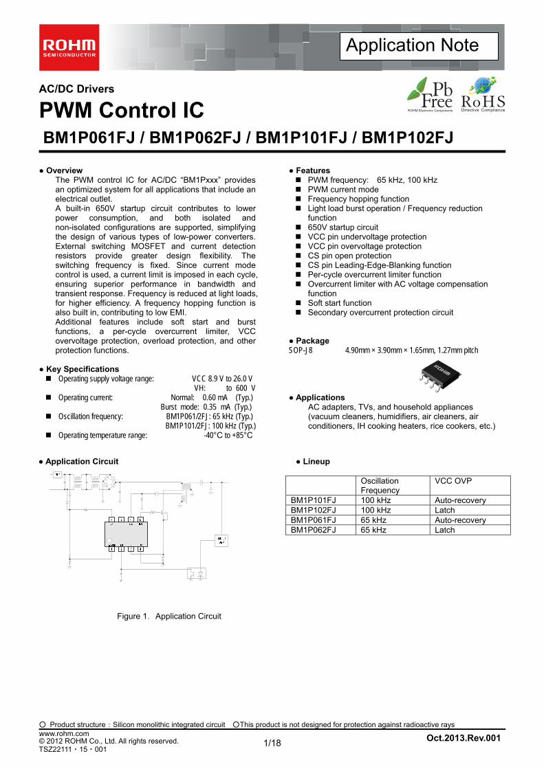
AC/DC Drivers
PWM Control IC BM1P061FJ / BM1P062FJ / BM1P101FJ / BM1P102FJ
Overview
The PWM control IC for AC/DC “BM1Pxxx” provides an optimized system for all applications that include an electrical outlet. A built-in 650V startup circuit contributes to lower power consumption, and both isolated and non-isolated configurations are supported, simplifying the design of various types of low-power converters. External switching MOSFET and current detection resistors provide greater design flexibility. The switching frequency is fixed. Since current mode control is used, a current limit is imposed in each cycle, ensuring superior performance in bandwidth and transient response. Frequency is reduced at light loads, for higher efficiency. A frequency hopping function is also built in, contributing to low EMI. Additional features include soft start and burst functions, a per-cycle overcurrent limiter, VCC overvoltage protection, overload protection, and other protection functions.
Key Specifications Operating supply voltage range: VCC 8.9 V to 26.0 V
VH: to 600 V Operating current: Normal: 0.60 mA (Typ.)
Burst mode: 0.35 mA (Typ.) Oscillation frequency: BM1P061/2FJ: 65 kHz (Typ.)
BM1P101/2FJ: 100 kHz (Typ.) Operating temperature range: -40°C to +85°C
Features PWM frequency: 65 kHz, 100 kHz PWM current mode Frequency hopping function Light load burst operation / Frequency reduction
function 650V startup circuit VCC pin undervoltage protection VCC pin overvoltage protection CS pin open protection CS pin Leading-Edge-Blanking function Per-cycle overcurrent limiter function Overcurrent limiter with AC voltage compensation
function Soft start function Secondary overcurrent protection circuit
Package SOP-J8 4.90mm × 3.90mm × 1.65mm, 1.27mm pitch Applications
AC adapters, TVs, and household appliances (vacuum cleaners, humidifiers, air cleaners, air conditioners, IH cooking heaters, rice cookers, etc.)
Application Circuit Lineup
Oscillation Frequency
VCC OVP
BM1P101FJ 100 kHz Auto-recovery BM1P102FJ 100 kHz Latch BM1P061FJ 65 kHz Auto-recovery BM1P062FJ 65 kHz Latch
Figure 1.Application Circuit
Application Note
2/28
DatasheetDatasheetBM1P061FJ / BM1P062FJ / BM1P101FJ / BM1P102FJ
Oct.2013.Rev.001© 2012 ROHM Co., Ltd. All rights reserved. www.rohm.com
TSZ22111・15・001
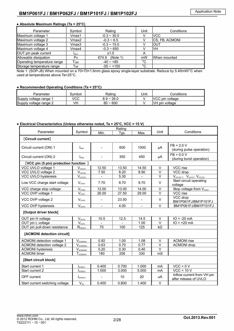
Absolute Maximum Ratings (Ta = 25°C)
Parameter Symbol Rating Unit Conditions Maximum voltage 1 Vmax1 -0.3 ~ 30.0 V VCC Maximum voltage 2 Vmax2 -0.3 ~ 6.5 V CS, FB, ACMONI Maximum voltage 3 Vmax3 -0.3 ~ 15.0 V OUT Maximum voltage 4 Vmax4 -0.3 ~ 650 V VH OUT pin peak current IOUT ±1.0 A Allowable dissipation Pd 674.9 (Note 1) mW When mounted Operating temperature range Topr -40 ~ +85 oC Storage temperature range Tstr -55 ~ +150 oC Note 1: (SOP-J8) When mounted on a 70×70×1.6mm glass epoxy single-layer substrate. Reduce by 5.40mW/°C when used at temperatures above Ta=25°C. Recommended Operating Conditions (Ta = 25°C)
Parameter Symbol Rating Unit Conditions Supply voltage range 1 VCC 8.9 ~ 26.0 V VCC pin voltage Supply voltage range 2 VH 80 ~ 600 V VH pin voltage Electrical Characteristics (Unless otherwise noted, Ta = 25°C, VCC = 15 V)
Parameter Symbol Rating
Unit Conditions Min. Typ. Max.
[Circuit current]
Circuit current (ON) 1 ION1 - 600 1000 μA FB = 2.0 V (during pulse operation)
Circuit current (ON) 2 ION2 - 350 450 μA FB = 0.0 V (during burst operation)
[VCC pin (5 pin) protection function ] VCC UVLO voltage 1 VUVLO1 12.50 13.50 14.50 V VCC rise VCC UVLO voltage 2 VUVLO2 7.50 8.20 8.90 V VCC drop VCC UVLO hysteresis VUVLO3 - 5.30 - V VUVLO3 = VUVLO1- VUVLO2
Low VCC charge start voltage VCHG1 7.70 8.70 9.70 V Start circuit operating
voltage VCC charge stop voltage VCHG2 12.00 13.00 14.00 V Stop voltage from VCHG1 VCC OVP voltage 1 VOVP1 26.00 27.50 29.00 V VCC rise
VCC OVP voltage 2 VOVP2 - 23.50 - V VCC drop BM1P061FJ/BM1P101FJ
VCC OVP hysteresis VOVP3 - 4.00 - V BM1P061FJ/BM1P101FJ
[Output driver block]
OUT pin H voltage VOUTH 10.5 12.5 14.5 V IO = -20 mA OUT pin L voltage VOUTL - - 1.00 V IO = +20 mA OUT pin pull-down resistance RPDOUT 75 100 125 kΩ
[ACMONI detection circuit]
ACMONI detection voltage 1 VACMONI1 0.92 1.00 1.08 V ACMONI rise ACMONI detection voltage 2 VACMONI2 0.63 0.70 0.77 V ACMONI drop ACMONI hysteresis VACMONI3 0.20 0.30 0.40 V ACMONI timer TACMONI1 180 256 330 mS
[Start circuit block]
Start current 1 ISTART1 0.400 0.700 1.000 mA VCC = 0 V Start current 2 ISTART2 1.000 3.000 5.000 mA VCC = 10 V
OFF current ISTART3 - 10 20 uA Inflow current from VH pin
after release of UVLO Start current switching voltage VSC 0.400 0.800 1.400 V
Application Note
3/28
DatasheetDatasheetBM1P061FJ / BM1P062FJ / BM1P101FJ / BM1P102FJ
Oct.2013.Rev.001© 2012 ROHM Co., Ltd. All rights reserved. www.rohm.com
TSZ22111・15・001
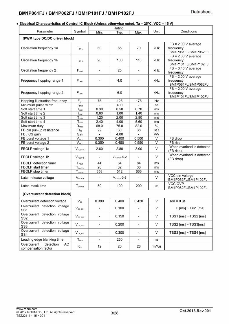
Electrical Characteristics of Control IC Block (Unless otherwise noted, Ta = 25°C, VCC = 15 V)
Parameter Symbol Rating
Unit Conditions Min. Typ. Max.
[PWM type DC/DC driver block]
Oscillation frequency 1a FSW1a 60 65 70 kHz FB = 2.00 V average
frequency BM1P061FJ/BM1P062FJ
Oscillation frequency 1b FSW1b 90 100 110 kHz FB = 2.00 V average
frequency BM1P101FJ/BM1P102FJ
Oscillation frequency 2 FSW2 - 25 - kHz FB = 0.40 V average
frequency
Frequency hopping range 1 FDEL1 - 4.0 - kHz FB = 2.00 V average
frequency BM1P061FJ/BM1P062FJ
Frequency hopping range 2 FDEL2 - 6.0 - kHz FB = 2.00 V average
frequency BM1P101FJ/BM1P102FJ
Hopping fluctuation frequency FCH 75 125 175 Hz Minimum pulse width Tmin - 400 - ns Soft start time 1 TSS1 0.30 0.50 0.70 ms Soft start time 2 TSS2 0.60 1.00 1.40 ms Soft start time 3 TSS3 1.20 2.00 2.80 ms Soft start time 4 TSS4 2.40 4.00 5.60 ms Maximum duty Dmax 68.0 75.0 82.0 % FB pin pull-up resistance RFB 22 30 38 kΩ FB / CS gain Gain - 4.00 - V/V FB burst voltage 1 VBST1 0.300 0.400 0.500 V FB drop FB burst voltage 2 VBST2 0.350 0.450 0.550 V FB rise
FBOLP voltage 1a VFOLP1A 2.60 2.80 3.00 V When overload is detected
(FB rise)
FBOLP voltage 1b VFOLP1B - VFOLP2A-0.2 - V When overload is detected
(FB drop) FBOLP detection timer TFOLP 44 64 84 ms FBOLP start timer TFOLP2 26 32 38 ms FBOLP stop timer TOLPST 358 512 666 ms
Latch release voltage VLATCH - VUVLO2-0.5 - V VCC pin voltage
BM1P062FJ/BM1P102FJ
Latch mask time TLATCH 50 100 200 us VCC OVP
BM1P062FJ/BM1P102FJ
[Overcurrent detection block]
Overcurrent detection voltage VCS 0.380 0.400 0.420 V Ton = 0 us
Overcurrent detection voltage SS1
VCS_SS1 - 0.100 - V 0 [ms] ~ Tss1 [ms]
Overcurrent detection voltage SS2
VCS_SS2 - 0.150 - V TSS1 [ms] ~ TSS2 [ms]
Overcurrent detection voltage SS3
VCS_SS3 - 0.200 - V TSS2 [ms] ~ TSS3[ms]
Overcurrent detection voltage SS4
VCS_SS4 - 0.300 - V TSS3 [ms] ~ TSS4 [ms]
Leading edge blanking time TLEB - 250 - ns
Overcurrent detection AC compensation factor
KCS 12 20 28 mV/us

4/28
DatasheetDatasheetBM1P061FJ / BM1P062FJ / BM1P101FJ / BM1P102FJ
Oct.2013.Rev.001© 2012 ROHM Co., Ltd. All rights reserved. www.rohm.com
TSZ22111・15・001
Pin Descriptions
Table1. I/O Pin Functions
No. Pin Name I/O Function ESD Diode
VCC GND
1 ACMONI I Comparator input pin 2 FB I Feedback signal input pin 3 CS I Primary current sense pin 4 GND I/O GND pin - 5 OUT O External MOS drive pin 6 VCC I/O Power supply input pin - 7 N.C. - Non Connection - - 8 VH I Start circuit pin -
I/O Equivalent Circuit Diagrams
Figure 2. I/O Equivalent Circuit Diagrams
Application Note
5/28
DatasheetDatasheetBM1P061FJ / BM1P062FJ / BM1P101FJ / BM1P102FJ
Oct.2013.Rev.001© 2012 ROHM Co., Ltd. All rights reserved. www.rohm.com
TSZ22111・15・001
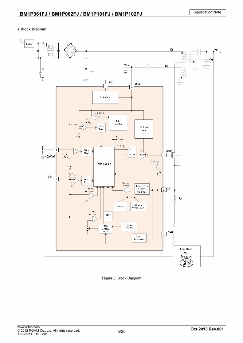
Block Diagram
Figure 3. Block Diagram
Application Note

6/28
DatasheetDatasheetBM1P061FJ / BM1P062FJ / BM1P101FJ / BM1P102FJ
Oct.2013.Rev.001© 2012 ROHM Co., Ltd. All rights reserved. www.rohm.com
TSZ22111・15・001
0.0
0.1
0.2
0.3
0.4
0.5
0.6
0.7
0.8
0.9
1.0
0 5 10 15 20 25 30 35 40 45 50
起動
時間
[sec]
Cvcc [uF]
Application Description for Each Block (1) Startup Circuit (VH pin: Pin 8)
These ICs integrate a startup circuit (650V withstand voltage), enabling both low standby power and high-speed startup. The startup circuit operates only at startup. Current flow during operation is shown in Figure 5. After startup, the only power consumed is due to the idling current ISTART3 (10uA typ.).
Ex.) When Vac=100V, startup power consumption is: PVH=100V*√2*10uA =1.41mW
Ex.) When Vac=240V, startup power consumption is:
PVH=240V*√2*10uA=3.38mW
Startup time is determined based on VH pin inrush current and VCC pin capacitance. Startup time reference values are shown in Figure 6. For example, when Cvcc=10uF, startup takes about 0.07 seconds. When the VCC pin has been shorted to GND, the ISTART1 current in Figure 5 flows. When the VH pin has been shorted to GND, a large current flows to GND from the VH line. To prevent this, please insert resistor RVH (5 kΩ ~ 60 kΩ) to limit the current between the VH line and the IC’s VH pin. When the VH pin is shorted, power equal to VH2/RVH is applied to the resistor. Therefore, select a resistor size that is able to tolerate this amount of power. If one resistor is not enough to withstand the amount of power dissipation, two or more resistors can be connected in series.
Figure 4. Startup Circuit Block Diagram
Figure 5. Startup Current vs VCC Voltage Figure 6. Startup Time (Reference)
(*Startup current flows from the VH pin.) (CVCC is capacitance at the VCC pin.)
The operating waveforms during startup are as follows.
Application Note
7/28
DatasheetDatasheetBM1P061FJ / BM1P062FJ / BM1P101FJ / BM1P102FJ
Oct.2013.Rev.001© 2012 ROHM Co., Ltd. All rights reserved. www.rohm.com
TSZ22111・15・001
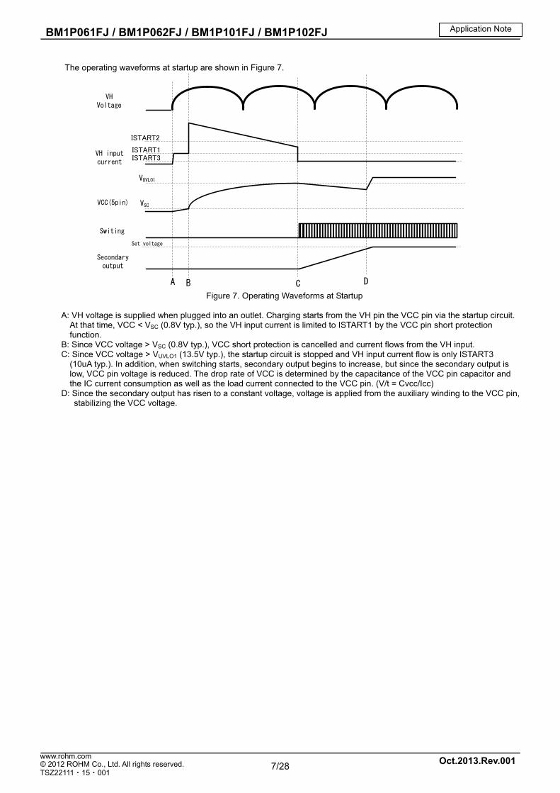
The operating waveforms at startup are shown in Figure 7.
Secondaryoutput
Switing
VHVoltage
VCC(5pin)
VH input current
A B C
VUVLO1
ISTART1ISTART3
ISTART2
Set voltage
VSC
D
Figure 7. Operating Waveforms at Startup
A: VH voltage is supplied when plugged into an outlet. Charging starts from the VH pin the VCC pin via the startup circuit. At that time, VCC < VSC (0.8V typ.), so the VH input current is limited to ISTART1 by the VCC pin short protection function.
B: Since VCC voltage > VSC (0.8V typ.), VCC short protection is cancelled and current flows from the VH input. C: Since VCC voltage > VUVLO1 (13.5V typ.), the startup circuit is stopped and VH input current flow is only ISTART3
(10uA typ.). In addition, when switching starts, secondary output begins to increase, but since the secondary output is low, VCC pin voltage is reduced. The drop rate of VCC is determined by the capacitance of the VCC pin capacitor and the IC current consumption as well as the load current connected to the VCC pin. (V/t = Cvcc/Icc)
D: Since the secondary output has risen to a constant voltage, voltage is applied from the auxiliary winding to the VCC pin, stabilizing the VCC voltage.
Application Note
8/28
DatasheetDatasheetBM1P061FJ / BM1P062FJ / BM1P101FJ / BM1P102FJ
Oct.2013.Rev.001© 2012 ROHM Co., Ltd. All rights reserved. www.rohm.com
TSZ22111・15・001
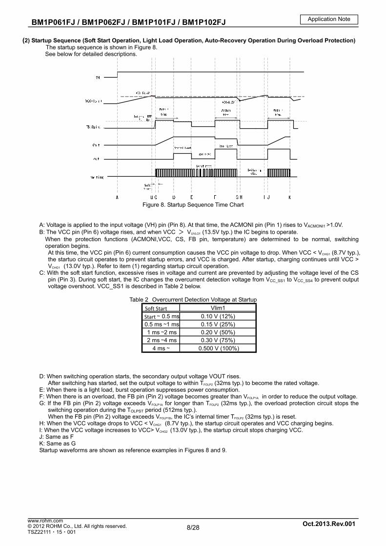
(2) Startup Sequence (Soft Start Operation, Light Load Operation, Auto-Recovery Operation During Overload Protection) The startup sequence is shown in Figure 8. See below for detailed descriptions.
Figure 8. Startup Sequence Time Chart
A: Voltage is applied to the input voltage (VH) pin (Pin 8). At that time, the ACMONI pin (Pin 1) rises to VACMONI1 >1.0V. B: The VCC pin (Pin 6) voltage rises, and when VCC > VUVLO1 (13.5V typ.) the IC begins to operate. When the protection functions (ACMONI,VCC, CS, FB pin, temperature) are determined to be normal, switching operation begins. At this time, the VCC pin (Pin 6) current consumption causes the VCC pin voltage to drop. When VCC < VCHG1 (8.7V typ.), the startuo circuit operates to prevent startup errors, and VCC is charged. After startup, charging continues until VCC > VCHG1 (13.0V typ.). Refer to item (1) regarding startup circuit operation.
C: With the soft start function, excessive rises in voltage and current are prevented by adjusting the voltage level of the CS pin (Pin 3). During soft start, the IC changes the overcurrent detection voltage from VCC_SS1 to VCC_SS4 to prevent output voltage overshoot. VCC_SS1 is described in Table 2 below.
Table 2 Overcurrent Detection Voltage at Startup
D: When switching operation starts, the secondary output voltage VOUT rises.
After switching has started, set the output voltage to within TFOLP2 (32ms typ.) to become the rated voltage. E: When there is a light load, burst operation suppresses power consumption. F: When there is an overload, the FB pin (Pin 2) voltage becomes greater than VFOLP1A in order to reduce the output voltage. G: If the FB pin (Pin 2) voltage exceeds VFOLP1A for longer than TFOLP2 (32ms typ.), the overload protection circuit stops the
switching operation during the TOLPST period (512ms typ.). When the FB pin (Pin 2) voltage exceeds VFOLP1B, the IC’s internal timer TFOLP2 (32ms typ.) is reset. H: When the VCC voltage drops to VCC < VCHG1 (8.7V typ.), the startup circuit operates and VCC charging begins. I: When the VCC voltage increases to VCC> VCHG2 (13.0V typ.), the startup circuit stops charging VCC. J: Same as F K: Same as G Startup waveforms are shown as reference examples in Figures 8 and 9.
Soft Start Vlim1
Start ~ 0.5 ms 0.10 V (12%)0.5 ms ~1 ms 0.15 V (25%)1 ms ~
2 ms 0.20 V (50%)
2 ms ~ 4 ms 0.30 V (75%)4 ms ~ 0.500 V (100%)
Application Note

9/28
DatasheetDatasheetBM1P061FJ / BM1P062FJ / BM1P101FJ / BM1P102FJ
Oct.2013.Rev.001© 2012 ROHM Co., Ltd. All rights reserved. www.rohm.com
TSZ22111・15・001
1. Parameter: Time 1. Parameter: Time
2. Channel: CH1 2. Channel: CH1 3. Cursor 1 3. Cursor 1 4. Cursor 2 4. Cursor 2 Figure 8. No-Load Startup Waveforms Figure 9. Heavy-Load Startup Waveforms
(3) VCC Pin Protection Function
This IC includes a VCC pin undervoltage protection function (UVLO), overvoltage protection function (OVP), as well as a VCC charge function that operates when the VCC voltage has dropped. The VCC UVLO and OVP functions prevent damage to the switching MOSFET due to insufficient/excessive VCC voltage. When the VCC voltage drops, the VCC charge function charges from a line with higher voltage than the start circuit and stabilizes secondary output.
(3-1) VCC UVLO and OVP Functions
VCC UVLO is an auto-recovery type comparator with voltage hysteresis. For VCC OVP, the BM1Pxx1 Series features an auto-recovery type comparator while the BM1Pxx2 Series utilizes a latch-type comparator. Latch release (reset) after latch operation detection by VCC OVP is triggered when VCC < VLATCH (7.7V typ.). This operation is shown in Figure 8. A mask time TLATCH (100us typ.) is built into VCC OVP. Detection is performed when the VCC pin (Pin 6) voltage continues to exceed VOVP1 (27.5V typ.) for TLATCH (100us typ.). This function masks surges and the like. (See section 7 below)
VCCuvlo1
ON
OFF
Vovp
VCCuvlo2
ON
OFF OFF
OFF
ON
OFF
A B C D E F
OFF
L : NormalH : Latch
G H I
Vlatch
VCCCHG2
VCCCHG1
TLATCH
AJ
ON
ON
OFF OFF
ON
ON ON ON
OFF OFF OFF
ON
OFF
K Figure 8. VCC UVLO / OVP Time Chart
Application Note
VCC voltage
VH voltage
Secondary output
VCC voltage
VH voltage
Secondary output
10/28
DatasheetDatasheetBM1P061FJ / BM1P062FJ / BM1P101FJ / BM1P102FJ
Oct.2013.Rev.001© 2012 ROHM Co., Ltd. All rights reserved. www.rohm.com
TSZ22111・15・001
A: Voltage is supplied to the VH pin (Pin 8) and voltage at the VCC pin (Pin 6) starts to rise. B: When the VCC pin (Pin 6) voltage > VUVLO1, the VCC UVLO function is canceled and DC/DC operation begins. C: When the VCC pin (Pin 6) voltage > VOVP, VCC OVP detects overvoltage in the IC. D: When the VCC pin (Pin 6) voltage > VOCP continues for TLATCH (100us typ.), switching is stopped by the VCC OVP function. (Latch mode) E: When the VCC pin (Pin 6) voltage < VCHG1, the VCC charge function operates and the VCC pin (Pin 6) voltage rises. F: When the VCC pin (pin 6) voltage > VCHG2, the VCC charge function is stopped. G: Same as E. H: Same as F. I: High voltage line VH is reduced. J: When VCC < VUVLO2, the VCC UVLO function operates. K: When VCC < VLATCH,, latch is cancelled.
• VCC Pin Capacitance Value To ensure stable operation of the IC, please set the VCC pin capacitance value to 10uF or greater. If the capacitor at the VCC pin is too large, the response of the VCC pin to the secondary output will be delayed. In cases
where the transformer has a low degree of coupling, a large surge can be generated at the VCC pin, which may damage the IC. In this case, insert a resistance of 10Ω to 100Ω on a bus between the diode and capacitor after the auxiliary winding. As for constants, perform a waveform evaluation of the VCC pin and determine values that will prevent any surges at the VCC pin from exceeding the absolute maximum rating.
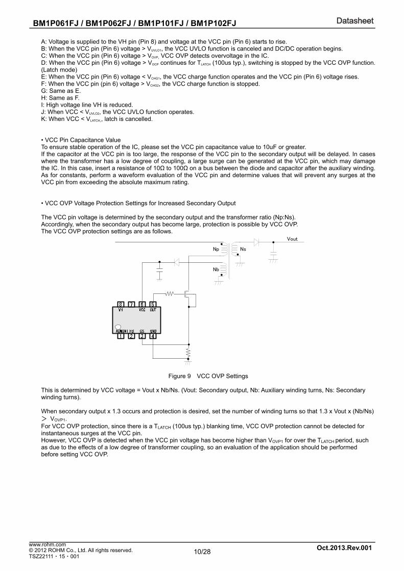
• VCC OVP Voltage Protection Settings for Increased Secondary Output The VCC pin voltage is determined by the secondary output and the transformer ratio (Np:Ns). Accordingly, when the secondary output has become large, protection is possible by VCC OVP. The VCC OVP protection settings are as follows.
Np
Nb
Ns
Vout
Figure 9 VCC OVP Settings
This is determined by VCC voltage = Vout x Nb/Ns. (Vout: Secondary output, Nb: Auxiliary winding turns, Ns: Secondary winding turns). When secondary output x 1.3 occurs and protection is desired, set the number of winding turns so that 1.3 x Vout x (Nb/Ns) > VOVP1. For VCC OVP protection, since there is a TLATCH (100us typ.) blanking time, VCC OVP protection cannot be detected for instantaneous surges at the VCC pin. However, VCC OVP is detected when the VCC pin voltage has become higher than VOVP1 for over the TLATCH period, such as due to the effects of a low degree of transformer coupling, so an evaluation of the application should be performed before setting VCC OVP.
11/28
DatasheetDatasheetBM1P061FJ / BM1P062FJ / BM1P101FJ / BM1P102FJ
Oct.2013.Rev.001© 2012 ROHM Co., Ltd. All rights reserved. www.rohm.com
TSZ22111・15・001
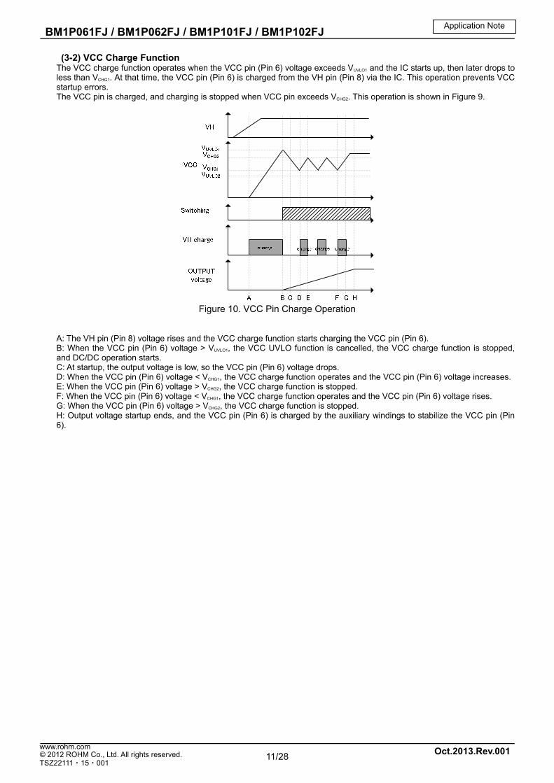
(3-2) VCC Charge Function The VCC charge function operates when the VCC pin (Pin 6) voltage exceeds VUVLO1 and the IC starts up, then later drops to
less than VCHG1. At that time, the VCC pin (Pin 6) is charged from the VH pin (Pin 8) via the IC. This operation prevents VCC startup errors. The VCC pin is charged, and charging is stopped when VCC pin exceeds VCHG2. This operation is shown in Figure 9.
Figure 10. VCC Pin Charge Operation
A: The VH pin (Pin 8) voltage rises and the VCC charge function starts charging the VCC pin (Pin 6). B: When the VCC pin (Pin 6) voltage > VUVLO1, the VCC UVLO function is cancelled, the VCC charge function is stopped, and DC/DC operation starts. C: At startup, the output voltage is low, so the VCC pin (Pin 6) voltage drops. D: When the VCC pin (Pin 6) voltage < VCHG1, the VCC charge function operates and the VCC pin (Pin 6) voltage increases. E: When the VCC pin (Pin 6) voltage > VCHG2, the VCC charge function is stopped. F: When the VCC pin (Pin 6) voltage < VCHG1, the VCC charge function operates and the VCC pin (Pin 6) voltage rises. G: When the VCC pin (Pin 6) voltage > VCHG2, the VCC charge function is stopped. H: Output voltage startup ends, and the VCC pin (Pin 6) is charged by the auxiliary windings to stabilize the VCC pin (Pin 6).
Application Note

12/28
DatasheetDatasheetBM1P061FJ / BM1P062FJ / BM1P101FJ / BM1P102FJ
Oct.2013.Rev.001© 2012 ROHM Co., Ltd. All rights reserved. www.rohm.com
TSZ22111・15・001
(4) ACMONI Pin Protection Function The ACMONI (Pin 1) is a brownout protection pin. The brownout function stops switching operation when the input AC voltage drops. An application example is shown in Figure 11. The input voltage utilizes a resistance divider. When the ACMONI pin exceeds VACOMONI (1.0V typ.), the circuit detects normal status and switching operation starts. After switching operation, when the ACMONI pin drops below VACMONI (0.7V typ.), the IC’s internal timer begins to operate. When the ACMONI pin stays below VACMONI (0.7V typ.) for at least TACMONI1 (256ms typ), DC/DC operation is turned off.
Therefore, even when AC voltage is interrupted, operation continues for a time equal to TACMONI1 (256ms typ.).
Figure 11. Application Circuit
The brownout setting can be set by connecting an external resistor to the ACMONI pin. The setting method is as follows. When the peak value of the AC line exceeds VHstart you should start operation by calculating the following: VHstart = (RH + RL) / RL x VACMONI1 *VACMONI1 = 1.0V
Set the RH and RL values according to this equation. At this time, the brownout end voltage VHend is determined as: VHend = (RH+RL) /RL x VACMONI2 *VACMONI1 = 0.7V
*When not using the brownout function, set the voltage to between VACMONI (1.0V typ.) and 5.0V.
Supply the voltage either externally or using a resistance divider from the VCC pin.
Np
Nb
Ns
Vout
Figure 12. Handling of the ACMONI Pin When Not Using the Brownout Function
RH
RL
Application Note
13/28
DatasheetDatasheetBM1P061FJ / BM1P062FJ / BM1P101FJ / BM1P102FJ
Oct.2013.Rev.001© 2012 ROHM Co., Ltd. All rights reserved. www.rohm.com
TSZ22111・15・001
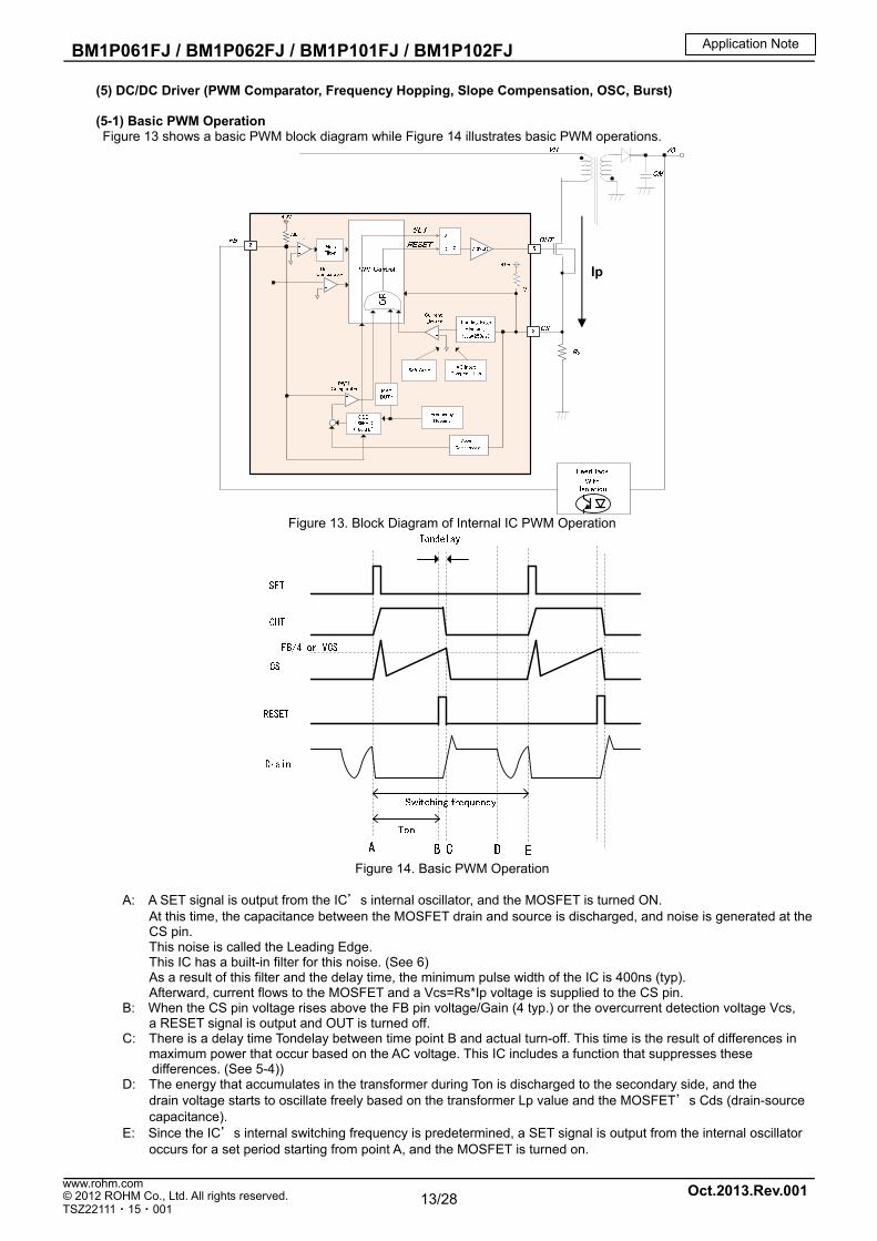
(5) DC/DC Driver (PWM Comparator, Frequency Hopping, Slope Compensation, OSC, Burst) (5-1) Basic PWM Operation Figure 13 shows a basic PWM block diagram while Figure 14 illustrates basic PWM operations.
Figure 13. Block Diagram of Internal IC PWM Operation
Figure 14. Basic PWM Operation
A: A SET signal is output from the IC’s internal oscillator, and the MOSFET is turned ON.
At this time, the capacitance between the MOSFET drain and source is discharged, and noise is generated at the CS pin.
This noise is called the Leading Edge. This IC has a built-in filter for this noise. (See 6) As a result of this filter and the delay time, the minimum pulse width of the IC is 400ns (typ).
Afterward, current flows to the MOSFET and a Vcs=Rs*Ip voltage is supplied to the CS pin. B: When the CS pin voltage rises above the FB pin voltage/Gain (4 typ.) or the overcurrent detection voltage Vcs, a RESET signal is output and OUT is turned off. C: There is a delay time Tondelay between time point B and actual turn-off. This time is the result of differences in maximum power that occur based on the AC voltage. This IC includes a function that suppresses these differences. (See 5-4)) D: The energy that accumulates in the transformer during Ton is discharged to the secondary side, and the drain voltage starts to oscillate freely based on the transformer Lp value and the MOSFET’s Cds (drain-source capacitance). E: Since the IC’s internal switching frequency is predetermined, a SET signal is output from the internal oscillator occurs for a set period starting from point A, and the MOSFET is turned on.
Application Note
Ip

14/28
DatasheetDatasheetBM1P061FJ / BM1P062FJ / BM1P101FJ / BM1P102FJ
Oct.2013.Rev.001© 2012 ROHM Co., Ltd. All rights reserved. www.rohm.com
TSZ22111・15・001
(5-2) Frequency Operation
Figure 15. PWM Operation in the IC
The PWM frequency is generated by the OSC block (internal oscillator) in Figure 15.
This oscillator has a switching frequency hopping function and the switching frequency fluctuates as is shown in Figure 16. The fluctuation cycle is 125Hz. Due to the frequency hopping function, the frequency spectrum is dispersed and the frequency spectrum peak is reduced. This increases the margin for EMI testing.
Figure 16-1. Frequency Hopping Function (BM1P06x Series) Figure 16-2. Frequency Hopping Function (BM1P10x Series) In Figure 16, the duty is calculated as Ton * Switching frequency * 100. The maximum duty value is Dmax (75% typ.).
Since PWM current mode is being used, sub-harmonic oscillation may occur if the duty exceeds 50%. Therefore, 22mV/us slope compensation is built in as a countermeasure.
To reduce power consumption during light loads, burst mode and frequency reduction circuits are included. These operations are illustrated in Figure17. As shown in this figure, the frequency fluctuates based on the FB voltage. If the FB voltage is within the range indicated in mode 2, switching loss is reduced by reducing the number of internal
oscillations based on the FB voltage.
Application Note

15/28
DatasheetDatasheetBM1P061FJ / BM1P062FJ / BM1P101FJ / BM1P102FJ
Oct.2013.Rev.001© 2012 ROHM Co., Ltd. All rights reserved. www.rohm.com
TSZ22111・15・001
Figure 17-1. Operation Based on the FB Pin Voltage (BM1P06x Series) Figure 17-2. Operation Based on the FB Pin Voltage
(BM1P10x Series)
・mode1: Burst operation ・mode2: Frequency reduction operation (reduces maximum frequency.) ・mode3: Fixed frequency operation (operates at maximum frequency.) ・mode4: Overload operation (overload condition is detected and pulse operation is stopped.) (5-3) Overcurrent Detection Operation RFB (30kΩ typ.) is used to pull up the FB pin in response to the internal power supply (4.0V). When the load of the secondary output voltage (secondary load power) changes, the photocoupler current changes, and the FB pin voltage also changes. The FB voltage VFB is determined by the following equation: FB Voltage = 4V - IFB. (IFB: Photocoupler Current) For example, when the load becomes heavier, the FB current is reduced and the FB voltage rises. When the load becomes lighter, the FB current increases and the FB voltage drops. In this way, secondary power is monitored by the FB pin.
As the FB pin voltage is monitored, if the load becomes lighter (FB voltage drops), burst mode operation or frequency reduction operation is performed. Figure 18 shows the CS detection voltage with regard to FB voltage.
Figure 18 FB Voltage - CS Voltage Characteristics
When the FB voltage is less than 2.0V or when the CS voltage exceeds the FB voltage/Gain (4 typ.), the MOSFET is turned off.
(See time point C in Figure 14.) When the FB voltage exceeds 2.0V, the CS voltage = Vcs + Kcs*Ton. Kcs*Ton depends on AC voltage compensation.
(See 5-4) Therefore, the peak current Ip is determined as Ip=Vcs1/Rs. The current value for the MOSFET should be set with sufficient margin, taking into account the Ip value obtained from this formula.
Maximum power is determined as Pmax = 1/2 x Lp x Ip2 x Fsw. (Lp: Primary inductance value, Ip: Primary peak current, Fsw: Switching frequency)
Vcs1 is determined as Vcs1 = Vcs (0.4V typ.) + Kcs (typ.= 20) * Ton + Vdelay. Vdelay is the amount of CS voltage increase during the delay time Rondelay between B and C in Figure 14.
This is calculated as Vdelay = Vin / Lp * Tondelay * Rs.
⊿CS/⊿FB Gain : 1/4
16/28
DatasheetDatasheetBM1P061FJ / BM1P062FJ / BM1P101FJ / BM1P102FJ
Oct.2013.Rev.001© 2012 ROHM Co., Ltd. All rights reserved. www.rohm.com
TSZ22111・15・001
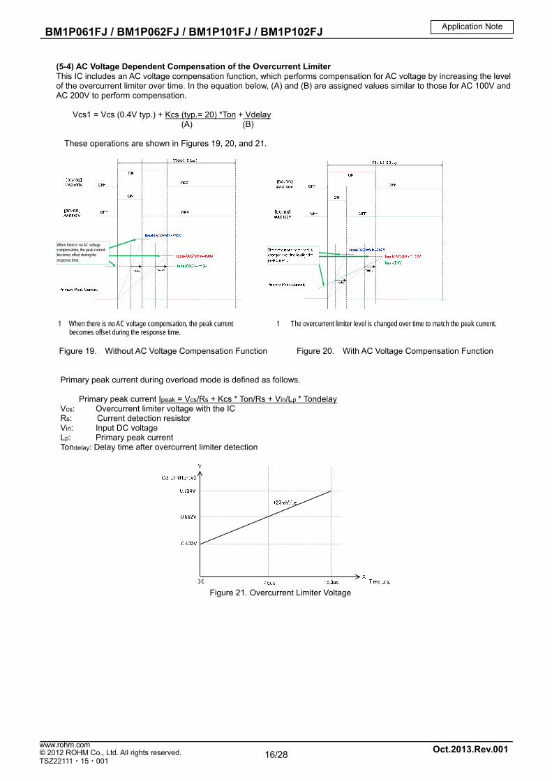
(5-4) AC Voltage Dependent Compensation of the Overcurrent Limiter This IC includes an AC voltage compensation function, which performs compensation for AC voltage by increasing the level of the overcurrent limiter over time. In the equation below, (A) and (B) are assigned values similar to those for AC 100V and AC 200V to perform compensation.
Vcs1 = Vcs (0.4V typ.) + Kcs (typ.= 20) *Ton + Vdelay
(A) (B) These operations are shown in Figures 19, 20, and 21.
When there is no AC voltage compensation, the peak currentbecomes offset during the response time.
1 When there is no AC voltage compensation, the peak current 1 The overcurrent limiter level is changed over time to match the peak current. becomes offset during the response time.
Figure 19. Without AC Voltage Compensation Function Figure 20. With AC Voltage Compensation Function
Primary peak current during overload mode is defined as follows.
Primary peak current Ipeak = Vcs/Rs + Kcs * Ton/Rs + Vin/Lp * Tondelay Vcs: Overcurrent limiter voltage with the IC Rs: Current detection resistor Vin: Input DC voltage Lp: Primary peak current Tondelay: Delay time after overcurrent limiter detection
Figure 21. Overcurrent Limiter Voltage
Application Note

17/28
DatasheetDatasheetBM1P061FJ / BM1P062FJ / BM1P101FJ / BM1P102FJ
Oct.2013.Rev.001© 2012 ROHM Co., Ltd. All rights reserved. www.rohm.com
TSZ22111・15・001
(6) L.E.B. Blanking Time When the drive MOSFET is turned on, a surge current is generated at time point A as shown in Figure 14. At that time, the CS voltage (Pin 4) rises, which may cause detection errors in the overcurrent limiter circuit.
To prevent this, the OUT pin in the IC is switched from low to high and the CS voltage (Pin 4) is masked for 250ns by the built-in L.E.B. (Leading Edge Blanking) function.
This blanking function can reduce the CS pin noise filter for noise generated when switching the OUT pin from low to high.
However, if the CS pin noise does not stay within this 250ns period, an RC filter should be applied to this pin, as is shown in Figure 22. At this time, a delay time occurs due to the RC filter when the CS pin is detected. Even if there is no filter, attaching an RCS is recommended as a countermeasure against surges. The recommended resistance for Rcs is 1 kΩ. When filtering is desired, adjust Ccs for this resistance.
Figure22. CS Pin Peripheral Circuit
(7) CS Pin Open Protection When the CS pin (Pin 4) becomes open, transient heat (due to noise, etc.) occurs in the IC, which may become damaged.
An open protection circuit has been built in to prevent such damage. (Auto-recovery protection)
NOUT
Leading Edge
Blanking
5 OUT
CS
RS
3
PREDriver
POUT
CURRENT SENSE
(V-V Change)
Normal : ×1.0
FBOLP_OH
S Q
R
VREF(4V)
1MΩ
VCCOVP
AND
AND
Timeout
ORBottom det
Figure 23. CS Pin Peripheral Circuit
Application Note

18/28
DatasheetDatasheetBM1P061FJ / BM1P062FJ / BM1P101FJ / BM1P102FJ
Oct.2013.Rev.001© 2012 ROHM Co., Ltd. All rights reserved. www.rohm.com
TSZ22111・15・001
(8) Output Overload Protection Function (FB OLP Comparator) As shown in mode4 of Figure 17, when the FB pin voltage rises to above a certain value, it is referred to as an overload condition.
The output overload protection function stops switching operation when mode4 is in overload mode. During an overload condition, the output voltage drops and so current no longer flows to the photocoupler while the FB voltage (Pin 2) rises. When the FB voltage (Pin 2) exceeds VFOLP1A (2.8V typ.) continuously for TFOLP2 (64ms typ.), an overload condition is determined to have occurred and switching is stopped. After the FB pin (Pin 2) exceeds VFOLP1A (2.8V typ.), if the FB pin voltage drops below VFOLP1B (2.6V typ.) during the TFOLP2
(64ms typ.) period, the overload protection timer is reset. Switching operations are performed during the TFOLP2 (32ms typ.) period. At startup, the FB pin (Pin 2) voltage is pulled up by a resistance to the IC internal voltage, and operation starts when the voltage reaches VFOLP1A (2.8V typ.) or above. Therefore, the startup time of secondary output voltage at startup must be set so that the FB voltage (Pin 2) drops to VFOLP1B (2.6V typ.) or below within the TFOLP2 (64ms typ) period. Once FBOLP is detected, recovery occurs after the TFOLP2 (512ms typ.) period.
Figure 24. Overload Protection (Auto-Recovery)
A: Since FB > VFOLP1A, the FBOLP comparator detects an overload. B: When the condition at A continues for TFOLP2 (32ms typ.), switching is stopped by the overload protection function. C: While switching has been stopped by the overload protection, the VCC voltage (Pin 6) drops and when the voltage at
the VCC pin (Pin 6) becomes less than VCHG, the VCC charge function operates to increase the VCC pin voltage. D: When the VCC charge function causes the VCC pin (Pin 6) voltage to rise above VCHG2, the VCC charge function is stopped. E: When the TOLPST (512ms typ.) period that starts from time point B elapses, switching is started via soft start operation. F: While an overload condition remains, FB continues to exceed VFOLP1A and switching is stopped when the period TFOLP2
(32ms) from time point E has elapsed. G: While switching is stopped, the VCC voltage (Pin 1) drops and when the VCC pin (Pin 6) voltage < VCHG1, the
VCC charge function operates and the VCC pin voltage increases. H: When the VCC charge function causes the VCC pin (Pin 6) voltage to exceed VCHG2, the VCC charge function is stopped.
Application Note
19/28
DatasheetDatasheetBM1P061FJ / BM1P062FJ / BM1P101FJ / BM1P102FJ
Oct.2013.Rev.001© 2012 ROHM Co., Ltd. All rights reserved. www.rohm.com
TSZ22111・15・001
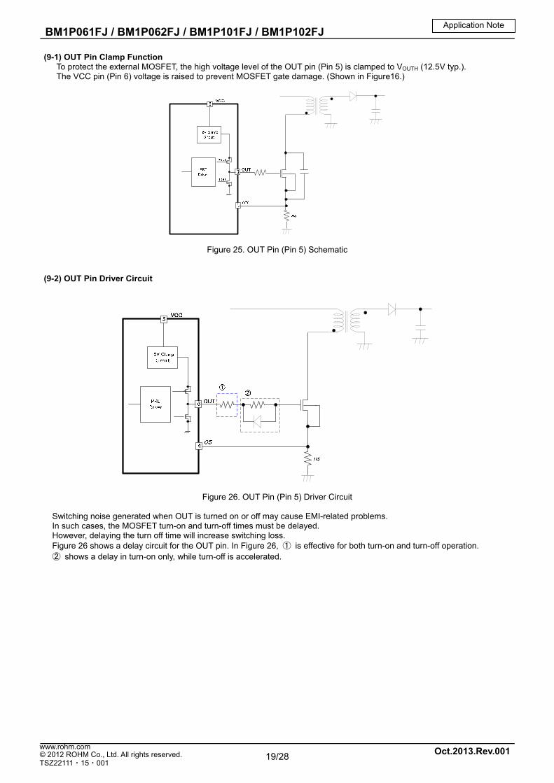
(9-1) OUT Pin Clamp Function To protect the external MOSFET, the high voltage level of the OUT pin (Pin 5) is clamped to VOUTH (12.5V typ.). The VCC pin (Pin 6) voltage is raised to prevent MOSFET gate damage. (Shown in Figure16.)
Figure 25. OUT Pin (Pin 5) Schematic
(9-2) OUT Pin Driver Circuit
Figure 26. OUT Pin (Pin 5) Driver Circuit
Switching noise generated when OUT is turned on or off may cause EMI-related problems. In such cases, the MOSFET turn-on and turn-off times must be delayed. However, delaying the turn off time will increase switching loss. Figure 26 shows a delay circuit for the OUT pin. In Figure 26, ① is effective for both turn-on and turn-off operation. ② shows a delay in turn-on only, while turn-off is accelerated.
Application Note
20/28
DatasheetDatasheetBM1P061FJ / BM1P062FJ / BM1P101FJ / BM1P102FJ
Oct.2013.Rev.001© 2012 ROHM Co., Ltd. All rights reserved. www.rohm.com
TSZ22111・15・001
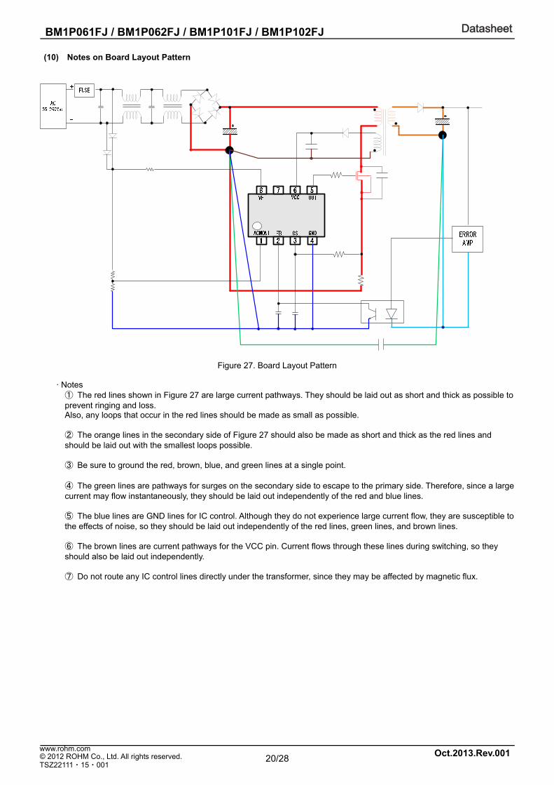
(10) Notes on Board Layout Pattern
Figure 27. Board Layout Pattern
· Notes ① The red lines shown in Figure 27 are large current pathways. They should be laid out as short and thick as possible to prevent ringing and loss. Also, any loops that occur in the red lines should be made as small as possible.
② The orange lines in the secondary side of Figure 27 should also be made as short and thick as the red lines and should be laid out with the smallest loops possible.
③ Be sure to ground the red, brown, blue, and green lines at a single point. ④ The green lines are pathways for surges on the secondary side to escape to the primary side. Therefore, since a large
current may flow instantaneously, they should be laid out independently of the red and blue lines.
⑤ The blue lines are GND lines for IC control. Although they do not experience large current flow, they are susceptible to the effects of noise, so they should be laid out independently of the red lines, green lines, and brown lines.
⑥ The brown lines are current pathways for the VCC pin. Current flows through these lines during switching, so they
should also be laid out independently. ⑦ Do not route any IC control lines directly under the transformer, since they may be affected by magnetic flux.

21/28
DatasheetDatasheetBM1P061FJ / BM1P062FJ / BM1P101FJ / BM1P102FJ
Oct.2013.Rev.001© 2012 ROHM Co., Ltd. All rights reserved. www.rohm.com
TSZ22111・15・001
Basic Characteristics (This data is for reference only and is not guaranteed.)
60.0
62.0
64.0
66.0
68.0
70.0
-40 -25 -10 5 20 35 50 65 80
TYP FREQ
[kHz]
Temp[ ]
65.0
67.0
69.0
71.0
73.0
75.0
77.0
79.0
81.0
83.0
85.0
-40 -25 -10 5 20 35 50 65 80
MAXDUTY1(TYP
周波
数時
)[%]
Temp[ ]
5.0
7.0
9.0
11.0
13.0
15.0
17.0
19.0
21.0
23.0
25.0
-40 -25 -10 5 20 35 50 65 80
MAXDUTY2(TYP
周波
数時
)[%]
Temp[ ] Max Duty 1 (Typ. frequency) [%] Max Duty 2 (Typ. frequency) [%] Fig-28-1 Switching Frequency (Typ.) Fig-28-2 MAXDUTY1 Fig-28-3 MAXDUTY2 (Soft Start)
15.0
17.0
19.0
21.0
23.0
25.0
27.0
29.0
31.0
33.0
35.0
-40 -25 -10 5 20 35 50 65 80
MAXDUTY3(TYP周
波数
時)[%]
Temp[ ]
0.60
0.70
0.80
0.90
1.00
1.10
1.20
1.30
1.40
-40 -25 -10 5 20 35 50 65 80
MAXDUTY
SS1(VCC=15)
[msec]
Temp[ ]
4.8
5.3
5.8
6.3
6.8
7.3
7.8
8.3
8.8
9.3
9.8
10.3
10.8
-40 -25 -10 5 20 35 50 65 80
MAXDUTY
SS2(VCC=15)[m
sec]
Temp[ ] Max Duty 3 (Typ. frequency) [%] Fig-28-4 MAXDUTY3 (Soft Start) Fig-28-5 Soft Start 1 Fig-28-6 Soft Start2
3.0
4.0
5.0
6.0
7.0
8.0
9.0
10.0
11.0
12.0
-40 -25 -10 5 20 35 50 65 80
NMOS RON(VCC=12)[Ω]
Temp[ ]
10.0
13.0
16.0
19.0
22.0
25.0
28.0
31.0
34.0
37.0
-40 -25 -10 5 20 35 50 65 80
PMOS RON(VCC=12)[Ω]
Temp[ ]
50.0
75.0
100.0
125.0
150.0
175.0
200.0
-40 -25 -10 5 20 35 50 65 80
TIMER
LATCH[us]
Temp[ ]
0.0
5.0
10.0
15.0
20.0
-40 -25 -10 5 20 35 50 65 80
ICC(VCC)OFF(VCC=12)[uA]
Temp[ ]
15.0
17.0
19.0
21.0
23.0
25.0
-40 -25 -10 5 20 35 50 65 80
FBRES(VCC=12)[kΩ
]
Temp[ ]
150.0
175.0
200.0
225.0
250.0
275.0
300.0
325.0
350.0
-40 -25 -10 5 20 35 50 65 80
FB OVP 256ms(VCC=12)[ms]
Temp[ ]
0.48
0.49
0.50
0.51
0.52
0.53
-40 -25 -10 5 20 35 50 65 80
CURLIM VOLTAGE(VCC=12)[V]
Temp[ ]
0.20
0.25
0.30
0.35
0.40
-40 -25 -10 5 20 35 50 65 80
FB Burst Voltage(VCC=12)[V]
Temp[ ] Fig-28-12 FB OVP 256 ms Fig-28-13 CURLIM VOLTAGE Fig-28-14 FB Burst Voltage
Fig-28-11 FBRES
Fig-28-7 NMOS RON (VCC = 15V) Fig-28-8 PMOS RON (VCC = 15V) Fig-28-9 TIMER LATCH
Fig-28-10 ICC (VCC) OFF (VCC = 15V)

22/28
DatasheetDatasheetBM1P061FJ / BM1P062FJ / BM1P101FJ / BM1P102FJ
Oct.2013.Rev.001© 2012 ROHM Co., Ltd. All rights reserved. www.rohm.com
TSZ22111・15・001
0.37
0.40
0.43
0.46
0.49
0.52
0.55
0.58
0.61
-40 -25 -10 5 20 35 50 65 80
COMP LATCH detect voltage[V]
Temp[ ]
‐5.00
‐3.00
‐1.00
1.00
3.00
5.00
-40 -25 -10 5 20 35 50 65 80
COMP LATCH detect
voltage error[%]
Temp[ ]
19.4
21.4
23.4
25.4
27.4
29.4
31.4
-40 -25 -10 5 20 35 50 65 80
COMP pull up RES(VCC=12)[kΩ]
Temp[ ] Figure 27 COMP LATCH Detect Voltage Figure 28 COMP LATCH Detect Voltage Error Figure 29 COMP Pull Up RES
‐5.0
‐3.0
‐1.0
1.0
3.0
5.0
-40 -25 -10 5 20 35 50 65 80
COMP pull up
RES
error(VCC=12)[%]
Temp[ ] Figure 30 COMP Pull Up RES Error Figure 31 RCOMP Figure 32 RCOMP Error
60.0
62.0
64.0
66.0
68.0
70.0
8.5 14.0 19.5 25.0
TYP FR
EQ[kHz]
VCC[V]
0.480
0.485
0.490
0.495
0.500
0.505
0.510
0.515
0.520
0.525
0.530
8.5 14.0 19.5 25.0
CURLIM VOLTAGE(VCC=12)[V]
VCC[V]
3.32
3.42
3.52
3.62
3.72
3.82
3.92
4.02
8.5 14.0 19.5 25.0
RCOMP(VCC=12)[kΩ]
VCC[V] Figure 33 TYP FREQ Figure 34 CURLIM VOLTAGE Figure 35 RCOMP
23/28
DatasheetDatasheetBM1P061FJ / BM1P062FJ / BM1P101FJ / BM1P102FJ
Oct.2013.Rev.001© 2012 ROHM Co., Ltd. All rights reserved. www.rohm.com
TSZ22111・15・001
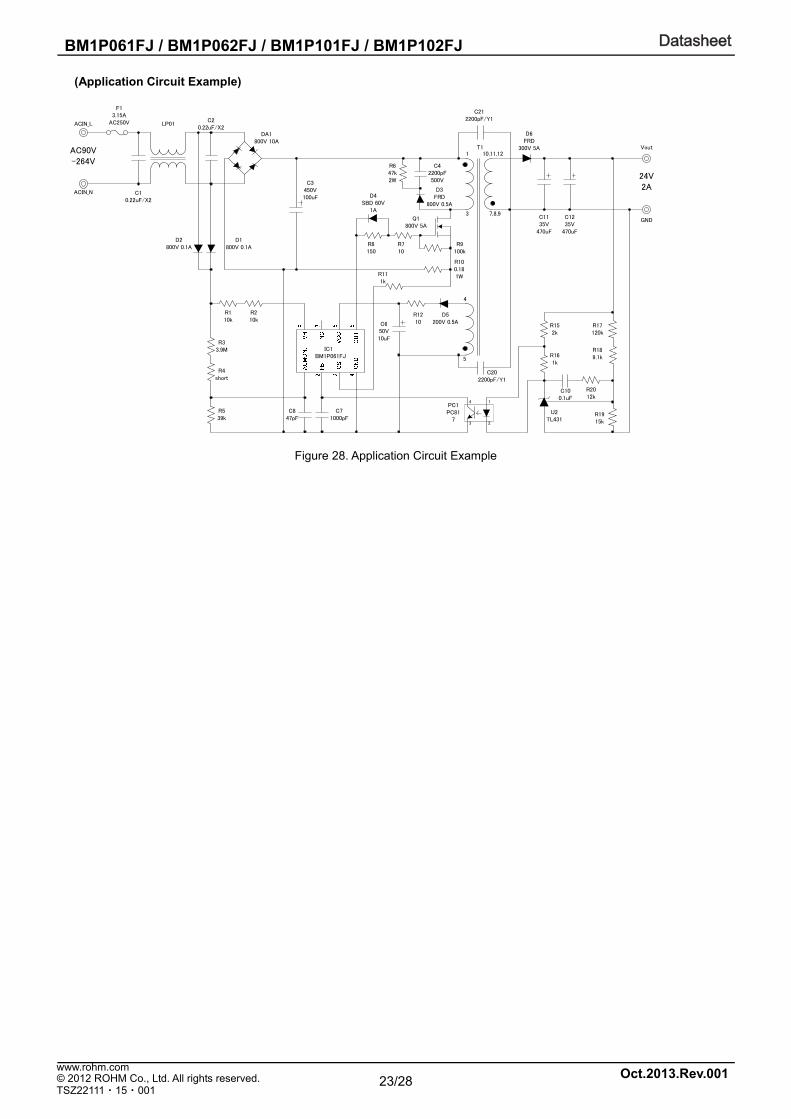
(Application Circuit Example)
R110k
R647k2W
D3FRD
800V 0.5A
Q1800V 5A
R710
R9100k
D5200V 0.5A
D6FRD
300V 5A
C1135V
470uF
R152k
R161k
R2012k
C100.1uF
U2TL431
R17120k
R1915k
T1
C42200pF500V
R100.181W
C650V10uF
C71000pF
1
3
5
10,11,12
7,8,9
C3450V100uF
PC1PC81
7
4
R111k
R189.1k
F13.15A
AC250V LP01
DA1800V 10A
R8150
R210k
R33.9M
R4short
R539k
C847pF
R1210
D2800V 0.1A
D4SBD 60V
1A
C202200pF/Y1
C10.22uF/X2
C20.22uF/X2
IC1BM1P061FJ
1
23
4
C212200pF/Y1
D1800V 0.1A
C1235V
470uF
AC90V-264V
ACIN_L
ACIN_N
24V2A
Vout
GND
Figure 28. Application Circuit Example

24/28
DatasheetDatasheetBM1P061FJ / BM1P062FJ / BM1P101FJ / BM1P102FJ
Oct.2013.Rev.001© 2012 ROHM Co., Ltd. All rights reserved. www.rohm.com
TSZ22111・15・001
Operation Modes of Protection Circuits
Table 3 lists the operation mode of each protection function.
Table 3. Protection Circuit Operation Modes
Function Operation Mode
VCC Undervoltage Lock Out Auto-recovery
VCC Overvoltage Protection BM1Pxx1 Series: Auto-recovery (with 100us timer) BM1Pxx2 Series: Latch (with 100us timer)
FB Over Limit Protection Auto-recovery (with 64us timer)
CS OPEN Protection Auto-recovery (with 100us timer)
Sequence
The IC sequence is shown in Figures 29 and 30. Transition to OFF mode occurs under all conditions when VCC exceeds 8.2V.
Soft Start1
Soft Start4
Burst & Low Power MODE
Normal MODE
OFF MODE
OLP MODE( Pulse Stop)
CS OPEN MODE
( Pulse Stop)
VCC OVP( Pulse Stop)
Soft Start2
Soft Start3
Figure 29. Sequence Diagram (BM1Pxx1 Series)
Application Note

25/28
DatasheetDatasheetBM1P061FJ / BM1P062FJ / BM1P101FJ / BM1P102FJ
Oct.2013.Rev.001© 2012 ROHM Co., Ltd. All rights reserved. www.rohm.com
TSZ22111・15・001
Figure 30. Sequence Diagram (BM1Pxx2 Series)
Application Note
26/28
DatasheetDatasheetBM1P061FJ / BM1P062FJ / BM1P101FJ / BM1P102FJ
Oct.2013.Rev.001© 2012 ROHM Co., Ltd. All rights reserved. www.rohm.com
TSZ22111・15・001
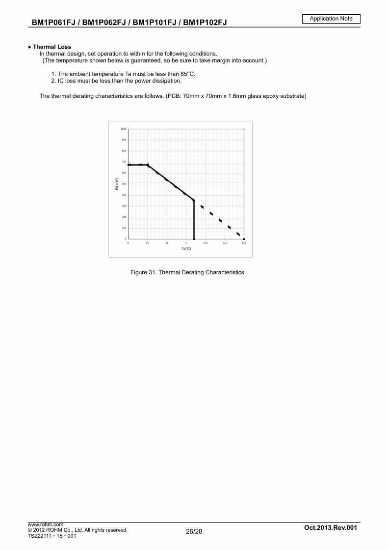
Thermal Loss
In thermal design, set operation to within for the following conditions. (The temperature shown below is guaranteed, so be sure to take margin into account.)
1. The ambient temperature Ta must be less than 85°C. 2. IC loss must be less than the power dissipation.
The thermal derating characteristics are follows. (PCB: 70mm x 70mm x 1.6mm glass epoxy substrate)
図-19 SOP8 熱軽減特性
Figure 31. Thermal Derating Characteristics
0
100
200
300
400
500
600
700
800
900
1000
0 25 50 75 100 125 150
Ta[]
Pd[
mW
]
Application Note

27/28
DatasheetDatasheetBM1P061FJ / BM1P062FJ / BM1P101FJ / BM1P102FJ
Oct.2013.Rev.001© 2012 ROHM Co., Ltd. All rights reserved. www.rohm.com
TSZ22111・15・001
Usage Precautions
(1) Absolute maximum ratings
Damage may occur if the absolute maximum ratings are exceeded, such as for applied voltage or operating temperature
range. Since the type of damage (short/open circuit, etc.) cannot be determined, in cases where a special mode may
conceivably exceed the absolute maximum ratings, please consider implementing physical safety measures such as fuses.
(2) Power supply and ground lines
In the board pattern design, route the power supply and ground lines to achieve low impedance. If there are multiple
power supply and ground lines, be careful about interference due to common impedance in the wiring pattern. With regard
to ground lines in particular, make sure to isolate large current and small signal routes, including the external circuits. Also,
for all of the power supply pins in this IC, in addition to inserting capacitors between the power supply and ground pins,
please thoroughly verify any problems associated with capacitor characteristics, such as capacitance loss at low
temperatures, before determining constants.
(3) Ground potential
Please set the ground pin potential to the minimum potential for all operating modes. (4) Pin shorts and mounting errors
When mounting the IC on a board, please pay attention to the orientation and direction of the IC and possible
misalignment. Incorrect mounting may damage the IC. Damage may also occur due to short circuit if foreign material is
introduced between IC pins, between a pin and the power supply, or between a pin and GND.
(5) Operation in strong magnetic fields
Please note that malfunction may occur if this product is used in a strong magnetic field.
(6) Input pins
In IC structures, parasitic elements are inevitably formed in relation to the potential. The operation of parasitic elements
can interfere with circuit operation, leading to malfunction and even damage. Therefore, please be careful to avoid usage
methods that enable parasitic elements to operate, such as by supplying a voltage lower than the ground voltage to the
input pin. Also, do not apply voltage to an input pin when there is no power supply voltage being supplied to the IC. In
fact, even if power supply voltage is being supplied, the voltage supplied to each input pin should be either below the
power supply voltage or within the guaranteed values in the electrical characteristics.
(7) External capacitors
When a ceramic capacitor is used as an external capacitor, please consider the possible drop in nominal capacitance
due to DC bias as well as capacitance fluctuation due to temperature and the like before determining constants.
(8) Thermal design
The thermal design should take into account the power dissipation (Pd) under actual conditions. Also, please ensure that
the output transistor does not exceed the rated voltage or ASO.
(9) Rush current
In a CMOS IC, rush current may momentarily flow if the internal logic is undefined when the power supply is turned ON,
so caution is needed with regard to the power supply coupling capacitance, the width of power supply and GND pattern
wires, and how they are laid out.
(10) Handling of test pins and unused pins
As noted in the function manual, application notes, and other documents, test pins and unused pins should be handled
so as not to cause problems under actual conditions. Please contact us regarding pins that are not otherwise described.
(11) Document contents
Documents such as application notes are design resources intended for use when designing applications, and as such
their contents are not guaranteed. Therefore, before finalizing an application, please conduct a thorough study and
evaluation, including of the external parts.
Regarding this document The Japanese version of this document is considered the formal specifications. Therefore, this translated version should be used only as a reference when reading the formal specifications. Accordingly, the formal specifications take priority regarding any differences that arise in the translation.
Application Note

28/28
DatasheetDatasheetBM1P061FJ / BM1P062FJ / BM1P101FJ / BM1P102FJ
Oct.2013.Rev.001© 2012 ROHM Co., Ltd. All rights reserved. www.rohm.com
TSZ22111・15・001
Part Number Selection
B M 1 P X X X F J - E 2
Part Number Package FJ: SOP-J8
Packaging and Forming SpecificationsE2: Reel-type embossed tape
Packaging Diagram and Forming Specifications 1 <Packaging Specifications> 2 Packaging Type Embossed tape 3 Package Quantity 4 Feed Direction 5 E2 (Direction: Pin 1 is at the upper left when holding the reel in the left hand and pulling the tape out with the right) 6 Reel 7 Pin 1 8 Feed Direction 9 Order in multiples of the package count Marking Diagram Lineup
Part No. (BM1PXXXFJ) BM1P101FJ BM1P102FJ BM1P061FJ BM1P062FJ
Lot No.
Pin 1 Mark
1PXXX
∗ Order quantity needs to be multiple of the minimum quantity.
<Tape and Reel information>
Embossed carrier tapeTape
Quantity
Direction of feed The direction is the 1pin of product is at the upper left when you hold
reel on the left hand and you pull out the tape on the right hand
2500pcs
E2
( )
Direction of feed
Reel1pin
(Unit : mm)
SOP-J8
4° +6°−4°
0.2±0.1
0.45
MIN
2 3 4
5678
1
4.9±0.2
0.545
3.9±
0.2
6.0±
0.3
(MAX 5.25 include BURR)
0.42±0.11.27
0.17
5
1.37
5±0.
1
0.1 S
S

R1102Awww.rohm.com© 2013 ROHM Co., Ltd. All rights reserved.
Notice
ROHM Customer Support System http://www.rohm.com/contact/
Thank you for your accessing to ROHM product informations. More detail product informations and catalogs are available, please contact us.
N o t e s
The information contained herein is subject to change without notice.
Before you use our Products, please contact our sales representative and verify the latest specifica-tions :
Although ROHM is continuously working to improve product reliability and quality, semicon-ductors can break down and malfunction due to various factors.Therefore, in order to prevent personal injury or fire arising from failure, please take safety measures such as complying with the derating characteristics, implementing redundant and fire prevention designs, and utilizing backups and fail-safe procedures. ROHM shall have no responsibility for any damages arising out of the use of our Poducts beyond the rating specified by ROHM.
Examples of application circuits, circuit constants and any other information contained herein are provided only to illustrate the standard usage and operations of the Products. The peripheral conditions must be taken into account when designing circuits for mass production.
The technical information specified herein is intended only to show the typical functions of and examples of application circuits for the Products. ROHM does not grant you, explicitly or implicitly, any license to use or exercise intellectual property or other rights held by ROHM or any other parties. ROHM shall have no responsibility whatsoever for any dispute arising out of the use of such technical information.
The Products are intended for use in general electronic equipment (i.e. AV/OA devices, communi-cation, consumer systems, gaming/entertainment sets) as well as the applications indicated in this document.
The Products specified in this document are not designed to be radiation tolerant.
For use of our Products in applications requiring a high degree of reliability (as exemplified below), please contact and consult with a ROHM representative : transportation equipment (i.e. cars, ships, trains), primary communication equipment, traffic lights, fire/crime prevention, safety equipment, medical systems, servers, solar cells, and power transmission systems.
Do not use our Products in applications requiring extremely high reliability, such as aerospace equipment, nuclear power control systems, and submarine repeaters.
ROHM shall have no responsibility for any damages or injury arising from non-compliance with the recommended usage conditions and specifications contained herein.
ROHM has used reasonable care to ensur the accuracy of the information contained in this document. However, ROHM does not warrants that such information is error-free, and ROHM shall have no responsibility for any damages arising from any inaccuracy or misprint of such information.
Please use the Products in accordance with any applicable environmental laws and regulations, such as the RoHS Directive. For more details, including RoHS compatibility, please contact a ROHM sales office. ROHM shall have no responsibility for any damages or losses resulting non-compliance with any applicable laws or regulations.
When providing our Products and technologies contained in this document to other countries, you must abide by the procedures and provisions stipulated in all applicable export laws and regulations, including without limitation the US Export Administration Regulations and the Foreign Exchange and Foreign Trade Act.
This document, in part or in whole, may not be reprinted or reproduced without prior consent of ROHM.
1)
2)
3)
4)
5)
6)
7)
8)
9)
10)
11)
12)
13)
14)
Top Related