


Languages
Pages
Legal


Module: Electronics I Module Number: 610/650221-222 Electronic Devices and Circuit Theory, 9th ed., Boylestad and Nashelsky
Lecturer: Dr. Omar Daoud Part II
Philadelphia University
Faculty of Engineering Communication and Electronics Engineering
Bipolar Junction Transistor
Configurations:
Common Base Configuration
Fig. 3.2 Types of transistors: (a) pnp; (b) npn.
Fig. 3.6 Notation and symbols used with the common-base configuration: npn transistor.
Fig. 3.8 Output or collector characteristics for a common-base transistor amplifier.

Module: Electronics I Module Number: 610/650221-222 Electronic Devices and Circuit Theory, 9th ed., Boylestad and Nashelsky
Lecturer: Dr. Omar Daoud Part II
Common Emitter Configuration
Common Collector Configuration
Fig. 3.13 Notation and symbols used with the common-emitter configuration: npn transistor
Fig. 3.14 Characteristics of a silicon transistor in the common-emitter configuration: (a) collector characteristics; (b) base characteristics.
Fig. 3.20 Notation and symbols used with the common-collector configuration: (a) pnp transistor; (b) npn transistor.

Module: Electronics I Module Number: 610/650221-222 Electronic Devices and Circuit Theory, 9th ed., Boylestad and Nashelsky
Lecturer: Dr. Omar Daoud Part II
Operating Point
Fixed Bias Circuit
Fig. 4.1 Various operating points within the limits of operation of a transistor.
Fig. 4.2 Fixed-bias circuit.
Fig. 4.3 DC equivalent of Fig. 4.2.

Module: Electronics I Module Number: 610/650221-222 Electronic Devices and Circuit Theory, 9th ed., Boylestad and Nashelsky
Lecturer: Dr. Omar Daoud Part II
Fig. 4.4 Base–emitter loop.
Fig. 4.5 Collector–emitter loop.
Fig. 4.7 DC fixed-bias circuit for Example 4.1.
Fig. 4.9 Determining ICsat. Fig. 4.10 Determining ICsat for the fixed-bias configuration.

Module: Electronics I Module Number: 610/650221-222 Electronic Devices and Circuit Theory, 9th ed., Boylestad and Nashelsky
Lecturer: Dr. Omar Daoud Part II
Emitter Bias
Fig. 4.17 BJT bias circuit with emitter resistor.
Fig. 4.18 Base–emitter loop.
Fig. 4.19 Network derived from the result of Fig. 4.18
Fig. 4.20 Reflected impedance level of RE.
Fig. 4.21 Collector–emitter loop.

Module: Electronics I Module Number: 610/650221-222 Electronic Devices and Circuit Theory, 9th ed., Boylestad and Nashelsky
Lecturer: Dr. Omar Daoud Part II
Emitter Bias
Fig. 4.14 Effect of an increasing level of RC on the load line
and the Q-point.
Fig. 4.15 Effect of lower values of VCC on the load line and the Q-point.

Module: Electronics I Module Number: 610/650221-222 Electronic Devices and Circuit Theory, 9th ed., Boylestad and Nashelsky
Lecturer: Dr. Omar Daoud Part II
Design Operation
Transistor Switching Network
Fig. 4.48 Example 4.19.
Fig. 4.49 Example 4.20.
Fig. 4.53 Transistor inverter.
Saturation conditions and the resulting terminal resistance.
Cutoff conditions and the
resulting terminal resistance.

Module: Electronics I Module Number: 610/650221-222 Electronic Devices and Circuit Theory, 9th ed., Boylestad and Nashelsky
Lecturer: Dr. Omar Daoud Part II
Fig. 4.56 Inverter for Example 4.24.
Fig. 4.57 Defining the time intervals of a pulse waveform.

Module: Electronics I Module Number: 610/650221-222 Electronic Devices and Circuit Theory, 9th ed., Boylestad and Nashelsky
Lecturer: Dr. Omar Daoud Part II
Philadelphia University Faculty of Engineering
Communication and Electronics Engineering
Bipolar Junction Transistor
AC Analysis: • A model is an equivalent circuit that represents the AC characteristics of the
transistor. • A model uses circuit elements that approximate the behavior of the transistor. • There are two models commonly used in small signal AC analysis of a
transistor: – re model – Hybrid equivalent model
The re Transistor Model:
BJTs are basically current-controlled devices, therefore the re model uses a diode and a current source to duplicate the behavior of the transistor. One disadvantage to this model is its sensitivity to the DC level. This model is designed for specific circuit conditions.
Common Base Configuration
Fig. 5.6 (a) Common-base BJT transistor; (b) re model for the configuration of (a).
Fig. 5.7 Common-base re equivalent circuit.
Fig. 5.9 Defining Av = Vo/Vi for the common-base configuration.

Module: Electronics I Module Number: 610/650221-222 Electronic Devices and Circuit Theory, 9th ed., Boylestad and Nashelsky
Lecturer: Dr. Omar Daoud Part II
Common Emitter Configuration
Common Collector Configuration Use the common-emitter model for the common-collector configuration.
Fig. 5.11 (a) Common-emitter BJT transistor; (b) approximate model for the configuration of a).
Fig. 5.17 re model for the common-emitter transistor configuration.
Fig. 5.12 Determining Zi using the approximate
Fig. 5.16 Determining the voltage and current gain for the common-emitter transistor amplifier.

Module: Electronics I Module Number: 610/650221-222 Electronic Devices and Circuit Theory, 9th ed., Boylestad and Nashelsky
Lecturer: Dr. Omar Daoud Part II
The Hybrid Equivalent Model: The following hybrid parameters are developed and used for modeling the transistor. These parameters can be found in a specification sheet for a transistor:
• hi = input resistance • hr = reverse transfer voltage ratio (Vi/Vo) ≅ 0 • hf = forward transfer current ratio (Io/Ii) • ho = output conductance ≅ ∞
Fig. 5.22 Complete hybrid equivalent circuit.
Fig. 5.23 Common-emitter configuration: (a) graphical symbol; (b) hybrid equivalent circuit
Fig. 5.24 Common-base configuration: (a) graphical symbol; (b) hybrid equivalent circuit.
Module: Electronics I Module Number: 610/650221-222 Electronic Devices and Circuit Theory, 9th ed., Boylestad and Nashelsky
Lecturer: Dr. Omar Daoud Part II
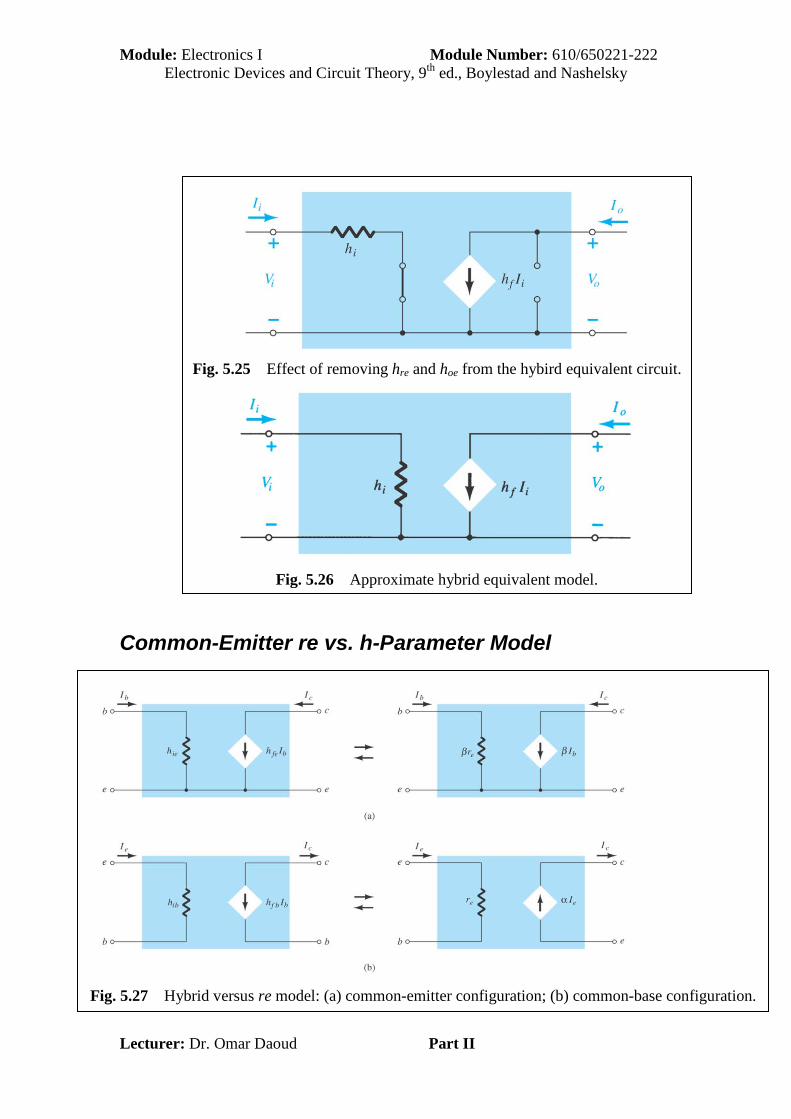
Common-Emitter re vs. h-Parameter Model
Fig. 5.25 Effect of removing hre and hoe from the hybird equivalent circuit.
Fig. 5.26 Approximate hybrid equivalent model.
Fig. 5.27 Hybrid versus re model: (a) common-emitter configuration; (b) common-base configuration.

Module: Electronics I Module Number: 610/650221-222 Electronic Devices and Circuit Theory, 9th ed., Boylestad and Nashelsky
Lecturer: Dr. Omar Daoud Part II
Philadelphia University
Faculty of Engineering Communication and Electronics Engineering
Bipolar Junction Transistor
BJT Amplifier Circuits:
Common Emitter Configurations:
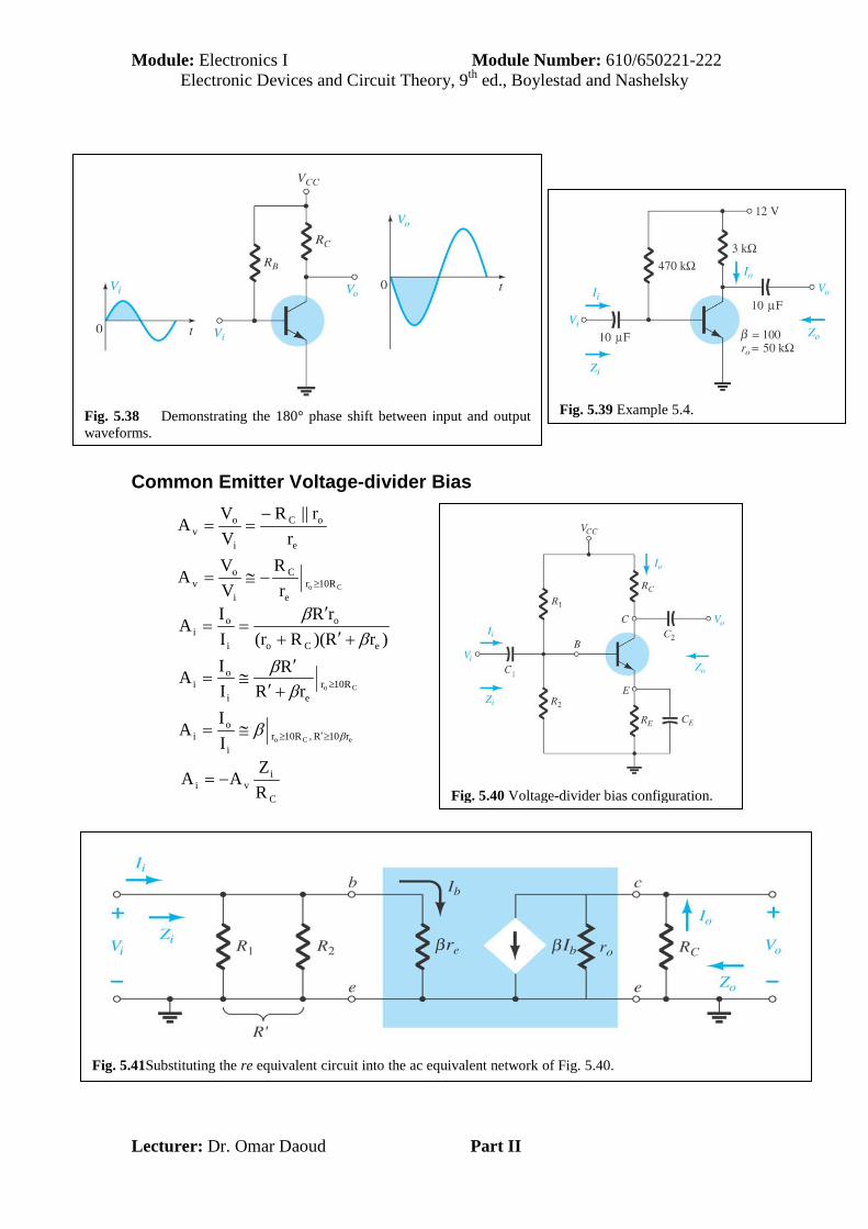
Common Emitter Fixed-bias • The input is applied to the base • The output is from the collector • High input impedance • Low output impedance • High voltage and current gain • Phase shift between input and output is 180°
Fig. 5.34 Common-emitter fixed-bias configuration.
Fig. 5.35 Network of Fig. 5.34 following the removal of the effects of VCC, C1 and C2.
Fig. 5.36 Substituting the re model into the network of Fig. 5.35.
Fig. 5.37Determining Zo for the network of Fig. 5.36.
Co 10Rre
Cv
e
oC
i
ov
r
RA
r)r||(R
VV
A
≥−=
−==
eBCo r10R ,10Rri
eBCo
oB
i
oi
A
)r)(RR(rrR
II
A
ββ
ββ
≥≥≅
++==
C
ivi R
ZAA −=
Module: Electronics I Module Number: 610/650221-222 Electronic Devices and Circuit Theory, 9th ed., Boylestad and Nashelsky
Lecturer: Dr. Omar Daoud Part II
Common Emitter Voltage-divider Bias
Fig. 5.39 Example 5.4.
Fig. 5.40 Voltage-divider bias configuration.
Fig. 5.41Substituting the re equivalent circuit into the ac equivalent network of Fig. 5.40.
eCo
Co
r10R ,10Rri
oi
10Rrei
oi
eCo
o
i
oi
II
A
rRR
II
A
)rR)(R(rrR
II
A
ββ
ββ
ββ
≥′≥
≥
≅=
+′′
≅=
+′+′
==
C
ivi R
ZAA −=
Co 10Rre
C
i
ov
e
oC
i
ov
rR
VV
A
rr||R
VV
A
≥−≅=
−==
Fig. 5.38 Demonstrating the 180° phase shift between input and output waveforms.

Module: Electronics I Module Number: 610/650221-222 Electronic Devices and Circuit Theory, 9th ed., Boylestad and Nashelsky
Lecturer: Dr. Omar Daoud Part II
Fig. 5.42 Example 5.5.
Common Emitter Bias
Fig. 5.43 CE emitter-bias configuration.
Fig. 5.46 Example 5.6.

Module: Electronics I Module Number: 610/650221-222 Electronic Devices and Circuit Theory, 9th ed., Boylestad and Nashelsky
Lecturer: Dr. Omar Daoud Part II
Common Base Configuration • The input is applied to the emitter. • The output is taken from the collector. • Low input impedance. • High output impedance. • Current gain less than unity. • Very high voltage gain. • No phase shift between input and output.
Fig. 5.44 Substituting the re equivalent circuit into the ac equivalent network of Fig. 5.43.
Eb
Eeb
RZE
C
i
ov
)R(rZEe
C
i
ov
b
C
i
ov
RR
VV
A
RrR
VV
A
ZR
VV
A
β
β
β
≅
+=
−≅=
+−==
−==
bB
B
i
oi ZR
RII
A+
==β
C
ivi R
ZAA −=
Fig. 5.46 Example 5.6.

Module: Electronics I Module Number: 610/650221-222 Electronic Devices and Circuit Theory, 9th ed., Boylestad and Nashelsky
Lecturer: Dr. Omar Daoud Part II
Fig. 5.57 Common-base configuration.
Fig. 5.58 Substituting the re equivalent circuit into the ac equivalent network of Fig. 5.57.
e
C
e
C
i
ov r
RrR
VV
A ≅==α
1II
Ai
oi −≅−== α
Fig. 5.59 Example 5.11.
Top Related