


Languages
Pages
Legal

1
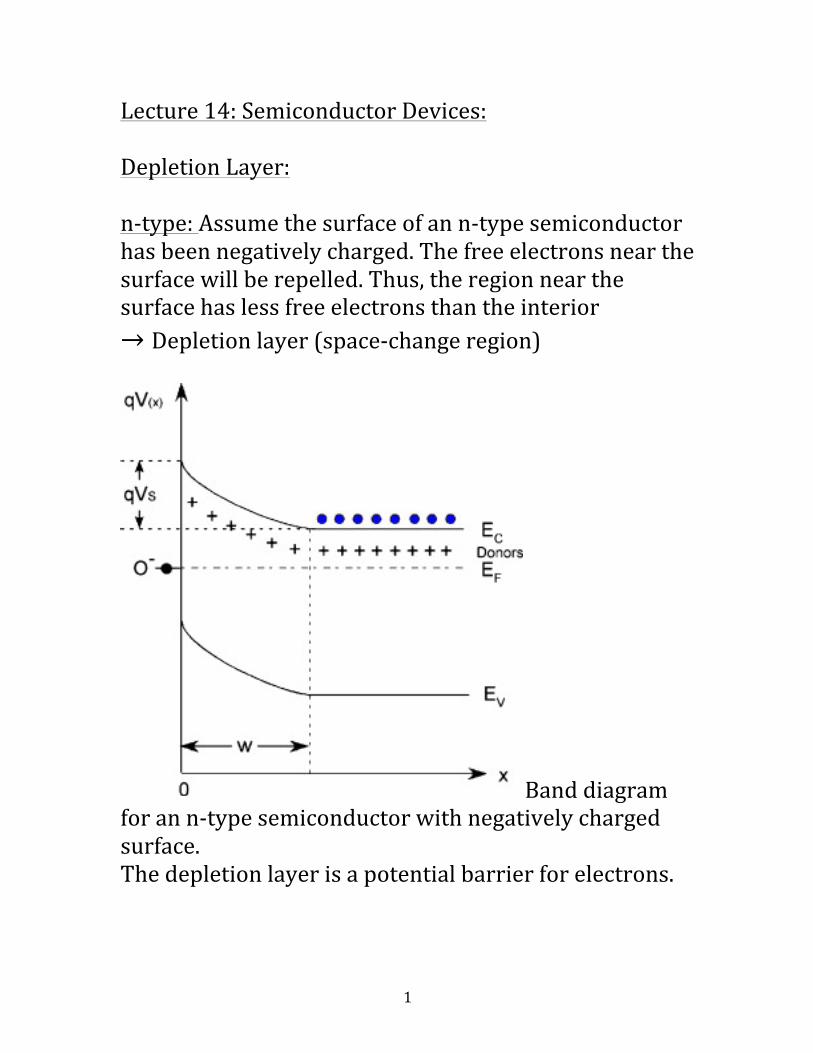
Lecture14:SemiconductorDevices:DepletionLayer:n‐type:Assumethesurfaceofann‐typesemiconductorhasbeennegativelycharged.Thefreeelectronsnearthesurfacewillberepelled.Thus,theregionnearthesurfacehaslessfreeelectronsthantheinterior→Depletionlayer(space‐changeregion)
Banddiagramforann‐typesemiconductorwithnegativelychargedsurface.Thedepletionlayerisapotentialbarrierforelectrons.

2
Banddiagramforap‐typesemiconductorwithpositivelychargedsurface.
Metalsemiconductorcontacts:n‐typemetal
1. SchottkyRectifier𝜑! > 𝜑!
2. Ohmiccontact𝜑! < 𝜑!

3
Rectifyingcontacts(Schottkybarriercontacts):n‐type
𝜑! > 𝜑!
Banddiagramforametalandn‐typesemiconductor𝜑:𝑤𝑜𝑟𝑘 𝑓𝑢𝑛𝑐𝑡𝑖𝑜𝑛
𝜑! > 𝜑!Ifthemetalandsemiconductorarebroughtintocontact,electronsflowfromthesemiconductorsdownintothemetaluntiltheFermienergiesofbothsidesareequal.

4

5
LooktothefollowingdrawingFig9‐16onbookThus,themetalwillbechargednegativelyandtheenergybandinthesemiconductorwillbelowered.Inequilibrium,electronsfrombothsidescrossthepotentialbarrier→DiffusionCurrentContactpotential:Thepotentialbarrierfortheelectronsdiffusingfromthesemiconductorintothemetal
𝜑! − 𝜑!Electronaffinity(X):Fromthebottomoftheconductionbandtotheionizationenergy.Driftcurrent:Whenanelectronholepairisthermallycreatedinornearthedepletionlayer.Theexcitedelectronsintheconductionbandissweptdownthebarrier,andsotheholes“thedriftcurrent”Note:thedriftcurrentisverysmallspecificallyforlargebandgap.Totalcurrent=diffusioncurrent+driftcurrent
6
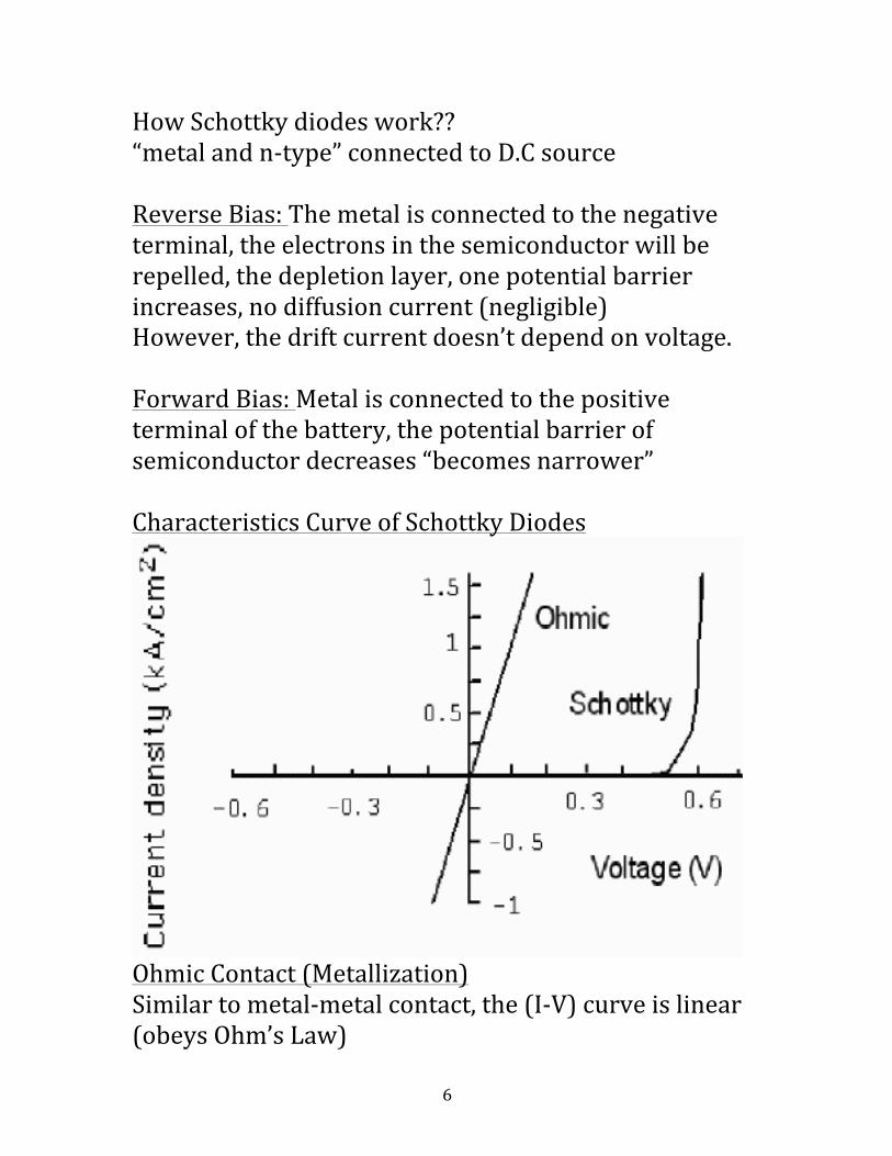
HowSchottkydiodeswork??“metalandn‐type”connectedtoD.CsourceReverseBias:Themetalisconnectedtothenegativeterminal,theelectronsinthesemiconductorwillberepelled,thedepletionlayer,onepotentialbarrierincreases,nodiffusioncurrent(negligible)However,thedriftcurrentdoesn’tdependonvoltage.ForwardBias:Metalisconnectedtothepositiveterminalofthebattery,thepotentialbarrierofsemiconductordecreases“becomesnarrower”CharacteristicsCurveofSchottkyDiodes
OhmicContact(Metallization)Similartometal‐metalcontact,the(I‐V)curveislinear(obeysOhm’sLaw)

7
Ohmiccontactcanoccurinmetal‐semiconductorcontactforthefollowingcases:
‐ metal‐ntype(if𝜑! < 𝜑!)

8
looktothefigure(9‐18)fromyourtextbook‐ metal‐ptype(if𝜑! > 𝜑!)
Metalp‐type:Similar
‐ Example:Al‐Siptype‐
Metaln‐type:Electronflowsfromthemetalintothesemiconductorandthebandsofsemiconductorbenddownward(nobarrier)electronflowsinthetwodirections.Thisconfigurationallowsthecurrenttoflowintoandoutofthesemiconductorwithoutpowerloss.

9
p‐njunction(diode):Similarpotentialbarriertoreactionisformed
10
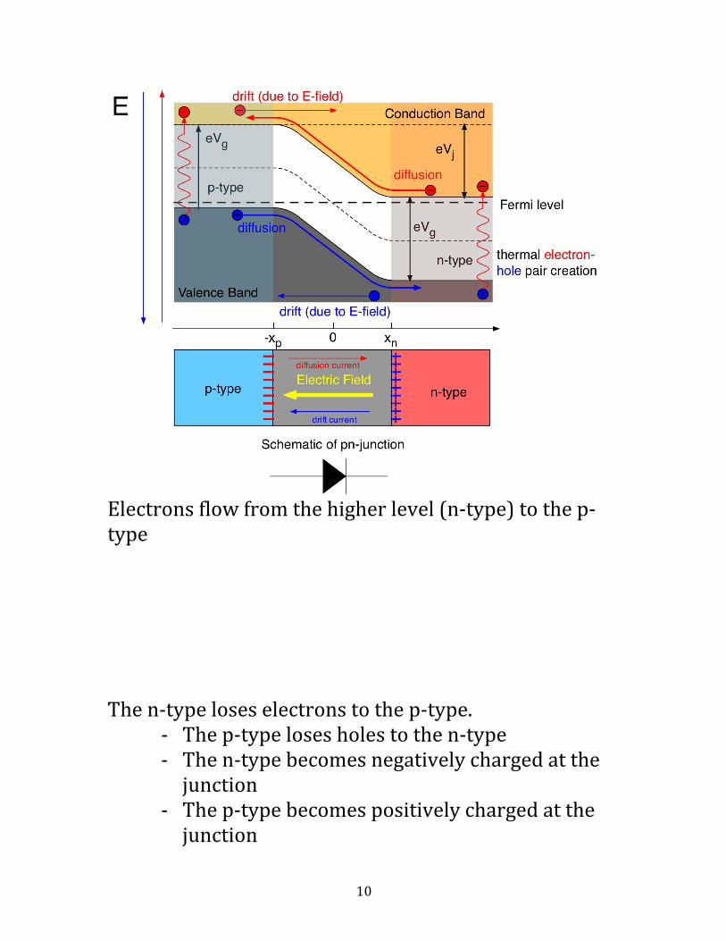
Electronsflowfromthehigherlevel(n‐type)tothep‐typeThen‐typeloseselectronstothep‐type.
‐ Thep‐typelosesholestothen‐type‐ Then‐typebecomesnegativelychargedatthejunction
‐ Thep‐typebecomespositivelychargedatthejunction

11
‐ AnelectricfieldisformedatthejunctionThisproceedsuntilequilibriumandbothFermienergiesareatthesamelevelNote:Thebandsmoveuptothep‐sideanddowntothen‐side

12
Lecture14a:ContinuesemiconductordevicesLet’scontinueonp‐njunctionp‐njunction(Diode):Semipotentialbarriertoreactionisformed

13
Electronsflowfromthehigherlevel(n‐type)tothep‐typeThen‐typeloseselectronstothep‐type.• Thep‐typelosesholestothen‐type• Then‐typebecomespositivelychargedatthejunction
• Thep‐typebecomesnegativelychargedatthejunction.
14
• Anelectricfieldisformedatthejunction
ThisproceedsuntilequilibriumisreachedandbothFermienergiesareatthesamelevel.Note:Thebandsmoveuptothep‐sideanddowntothen‐side
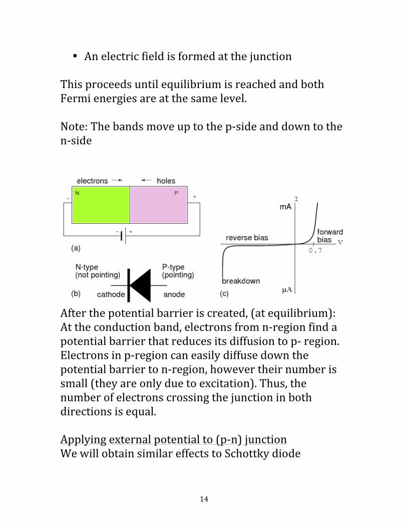
Afterthepotentialbarrieriscreated,(atequilibrium):Attheconductionband,electronsfromn‐regionfindapotentialbarrierthatreducesitsdiffusiontop‐region.Electronsinp‐regioncaneasilydiffusedownthepotentialbarrierton‐region,howevertheirnumberissmall(theyareonlyduetoexcitation).Thus,thenumberofelectronscrossingthejunctioninbothdirectionsisequal.Applyingexternalpotentialto(p‐n)junctionWewillobtainsimilareffectstoSchottkydiode

15
Looktothenextpageformoredetails
16
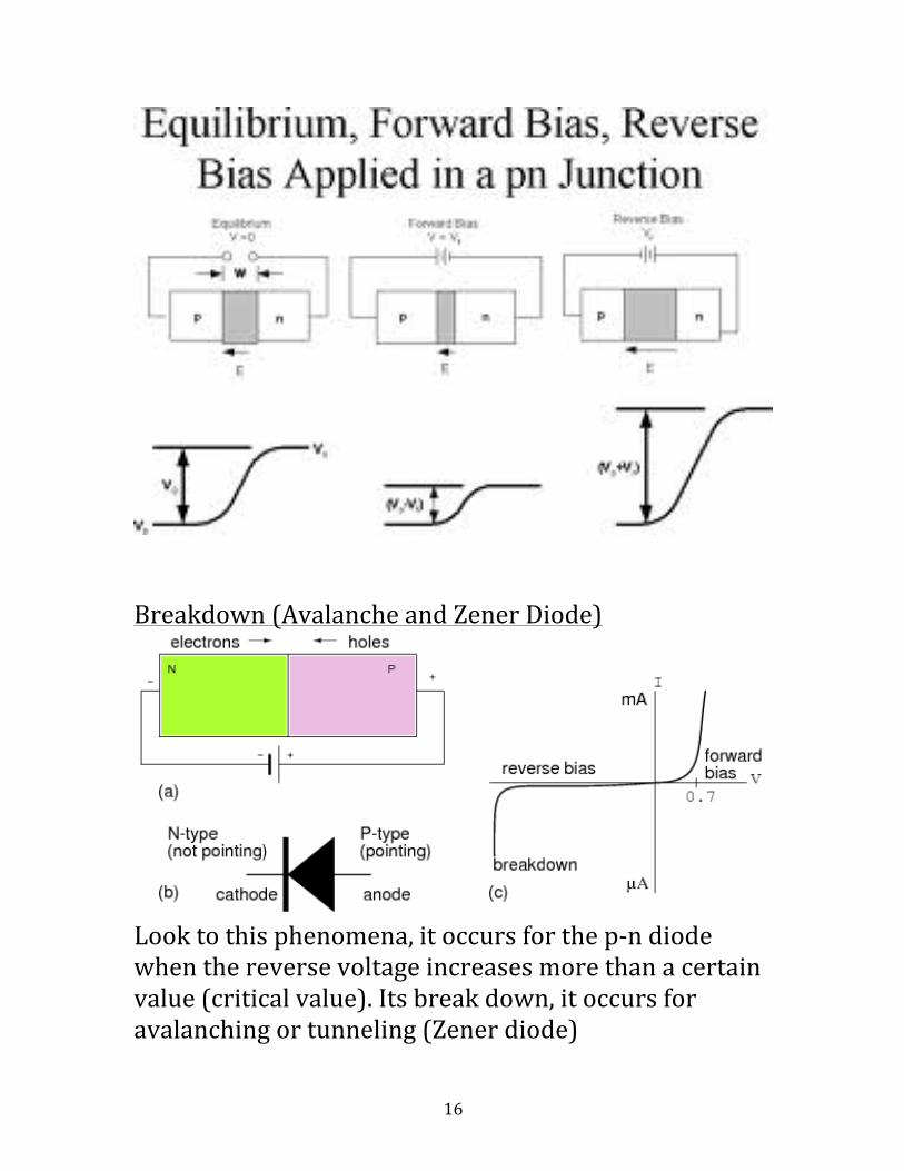
Breakdown(AvalancheandZenerDiode)
Looktothisphenomena,itoccursforthep‐ndiodewhenthereversevoltageincreasesmorethanacertainvalue(criticalvalue).Itsbreakdown,itoccursforavalanchingortunneling(Zenerdiode)

17
‐UsesforZenerDiode
Photodiode(solarcell)

18
Consistsofp‐njunction.Iflightfallsonornearthedepletedlayer,electronsareliftedfromthevalencebandtotheconductionband(electron‐holepairsarecreated).Let’slooktothebanddiagram
Theelectronswillmovetothen‐regionandtheholeswillmovetothep‐region.‐ wecandetectthesechargecarriersintwoways:
1. OpenCircuit(photovoltaicmodeofoperation)Anexternalpotentialwillappear

19
2. ShortCircuitthedevice(photo‐conductivemodeofoperation)
Anexternalcurrentwillflow
Thep‐regionismadeverythin(≈ 1nm),sothelightcanreachthedepletedlayer.Note:Defectsplayaseriousrole

20
AvalanchePhotodiode:p‐nphotodiodeoperatedinahighreversebias‐mode(nearbreakdownvoltage)Light→createelectron‐holepairs→areacceleratedthroughthedepletedregiontohighvelocity→ionizelatticeatomsandgeneratemorehole‐electronpairs=photocurrentgainTunnelDiode:Let’sdiscussfirst“degeneratesemiconductors”Atveryhighleveldoping,theFermilevelmovesupintotheconductionbandinthen‐typematerialandmovesdowntothevalenceinp‐typematerial.

21
Thephotodiodeisdegeneratep‐typeanddegeneraten‐typesemiconductor.Looktothefollowingfigure:
Anotherphenomena:Electronscantunnelthroughthepotentialbarrierinbothdirections.Inequilibriumthenettunnelcurrentiszero.LooktotheFermienergyineverymodeofoperationinthenextfigureandlooktotheresultantI‐Vcharacteristiccurveoftunneldiode

22

23
ReverseBias:PotentialbarrierisincreasedtheFermienergyinthep‐areaisraised.Electronsflowfromp‐typeton‐type.ForwardBias(small):Potentialbarrierisdecreased.Electronsflowfromn‐typetop‐typeForwardBias(Medium):Theareaopposite(facing)thefilledconductionbandisforbiddenthecurrentdecreasesForwardBias(normal):Electronsintheconductionbandgetenoughenergytoclimbthepotentialbarrierofp‐sideTransistorsThemostimportantelectronicdeviceBipolartransistorUnipolartransistor(fieldeffecttransistor)Bipolartransistor:twojunctions
n‐p‐ntransistorp‐n‐ptransistor
Bipolartransistor:carriersaremajorityandminorscurrentcontrolFieldeffectresistor:carriersareonlymajorityvoltagecontrolBipolarJunctionTransistor(n‐p‐n)

24
25
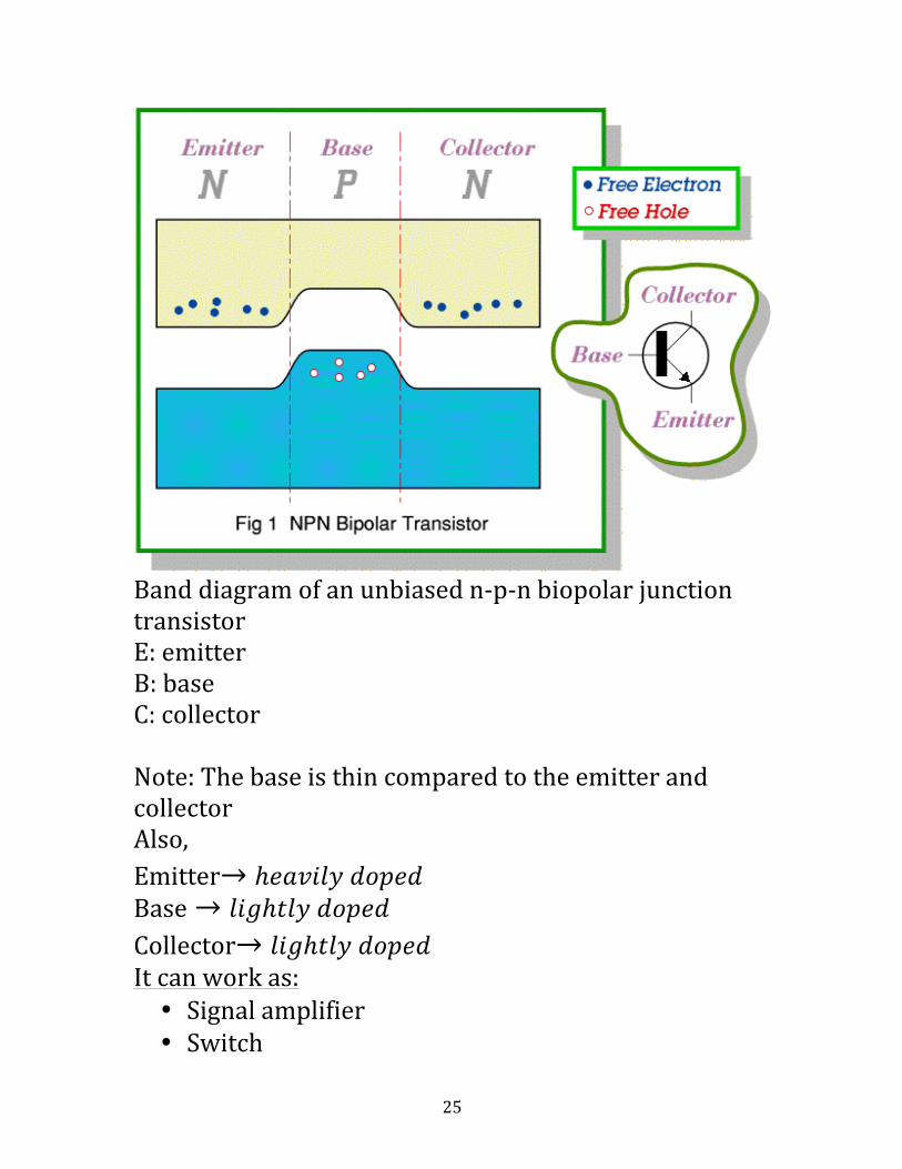
Banddiagramofanunbiasedn‐p‐nbiopolarjunctiontransistorE:emitterB:baseC:collectorNote:ThebaseisthincomparedtotheemitterandcollectorAlso,Emitter→ℎ𝑒𝑎𝑣𝑖𝑙𝑦 𝑑𝑜𝑝𝑒𝑑Base→𝑙𝑖𝑔ℎ𝑡𝑙𝑦 𝑑𝑜𝑝𝑒𝑑Collector→𝑙𝑖𝑔ℎ𝑡𝑙𝑦 𝑑𝑜𝑝𝑒𝑑Itcanworkas:• Signalamplifier• Switch
26
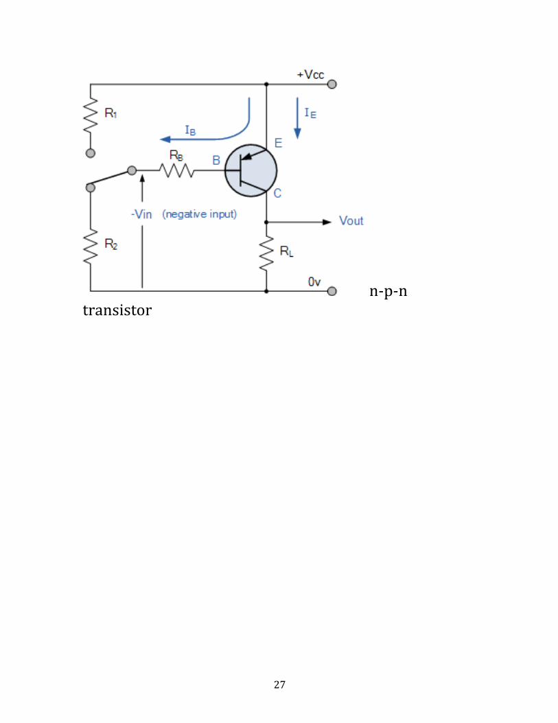
SignalAmplification:Emitterandbasediode:forwardbiasedBase‐collectordiode:reversebiasedLooktothefigureof:“Biasingann‐p‐ntransistor”‐ BecauseofforwardingbiasingtheE‐Bdiode,thebarrierwillbereduced,alargeelectronflowtothebase.
Whythebaseisthingandlightlydoped?Reversebiasingthebase‐collector→CausestheelectronstoacceleratedowntothecollectorSwitchingBasevoltagecanstoptheelectronflowfromtheemittertocollector
27
n‐p‐ntransistor
Top Related