


![SSD - ESOS LAB€¦ · SSD . 1 SSD Block Diagram 3.2 SSD NAND HDD . . SSD FTL . FTL NAND out-of-place update address mapping . Gabage Collection, Wear-leveling . 4. 4.1 SSD . Disksim[8]](https://static.fdocuments.us/doc/165x107/5ea6b67696cb1838a26c1ab1/ssd-esos-ssd-1-ssd-block-diagram-32-ssd-nand-hdd-ssd-ftl-ftl-nand-out-of-place.jpg)
Languages
Pages
Legal


1
GENUSION, Inc.
URL: http://www.genusion.co.jp
13th, Aug., 2013
B4-Flash Memory for SSD Applications - New Storage Arena with B4-Flash -

New Arena of Storage Device with B4-Flash
Low Latency
Scalable & High Density
Excellent Reliability
B4-Flash Features
Mobile XIP Flash
Completely Erasable
Data Storage
100 year SSD
Tier 0 SSD
New Arena of Storage Device
In Production

3
“B4-Flash” offers the Solution
for high featured Storage Devices with High Reliability, High Performance and
High Density
4
B4-Flash for Storage Solution
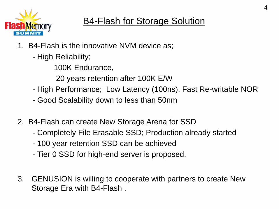
1. B4-Flash is the innovative NVM device as; - High Reliability; 100K Endurance, 20 years retention after 100K E/W - High Performance; Low Latency (100ns), Fast Re-writable NOR - Good Scalability down to less than 50nm 2. B4-Flash can create New Storage Arena for SSD - Completely File Erasable SSD; Production already started - 100 year retention SSD can be achieved - Tier 0 SSD for high-end server is proposed.
3. GENUSION is willing to cooperate with partners to create New Storage Era with B4-Flash .

5
B4-Flash Technology as innovative NVM

6
Vd=0V Vg=12V
Vwell=5V
3
Vg=12V
Vd=0V
1 Band-to-band-tunneling electron-hole pair generation (GIDL)
Vd=0V
Vwell=5V
2 Electron Acceleration
SiO2 barrier
3 Hot Electron Injection
SiO2
1 2
Vs=5V
Vg=12V
Vd=0V Vs=1.8V
1 2
3
P+ P+
N-well
B4-HE injection + Pch MOS transistor memory cell - Fastest Re-writable and Highly Scalable NOR Flash - High Endurance to 100K E/W and Excellent Retention of 20years after 100K E/W
Back Bias assisted Band to Band tunneling (B4) - Hot Electron Injection
B4-HE is the Innovation of Flash technology

7 B4-Flash Features
N+ N+ P-well
N+ N+ P-well
Cost: High Prog: Slow Erase: Slow
P+ P+ N-well
NOR
NAND
B4-Flash Memory
New Flash Mechanism
Performance : High
Cost: Low Prog: Fast Erase: Fast
Performance : Low
Performance: High Cost: Low Prog: Fast Erase: Fast
Reliability: Excellent

Programming Speed
100ns
1us
10us
100us
0.1MB/s 1MB/s 10MB/s 100MB/s
Ran
dom
Access
ConventionalNOR
B4-Flash
Fast Prog.
Fast Read
NAND
B4-Flash High Speed Program Capability
Small current and fast time of B4-Flash programming theoretically achieve 100MB/sec programming throughput.
<1n 1u 1m
Pro
gram
min
g Ti
me
(sec
)
Programming Current (A/cell)
100n
1u
10u
100u
1m
NAND (FN tunnel)
EEPROM (FN tunnel)
NOR, NROM (CHE)
MRAM, PRAM
source side injection
Worse
Better
B4-Flash(B4-HE)
B4-Flash Performance Create New Arena of Flash
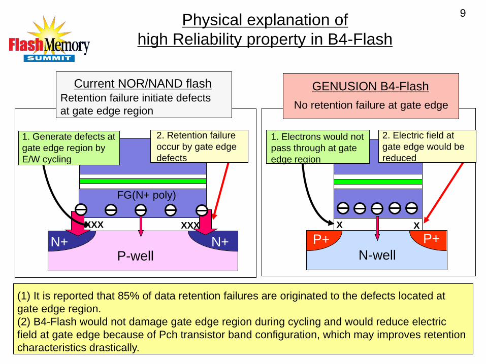
9 Physical explanation of high Reliability property in B4-Flash
P-well N+ N+
FG(N+ poly)
XXXX XXXX
N-well P+ P+
X X
1. Generate defects at gate edge region by E/W cycling
2. Retention failure occur by gate edge defects
1. Electrons would not pass through at gate edge region
Current NOR/NAND flash GENUSION B4-Flash
2. Electric field at gate edge would be reduced
Retention failure initiate defects at gate edge region No retention failure at gate edge
(1) It is reported that 85% of data retention failures are originated to the defects located at gate edge region. (2) B4-Flash would not damage gate edge region during cycling and would reduce electric field at gate edge because of Pch transistor band configuration, which may improves retention characteristics drastically.
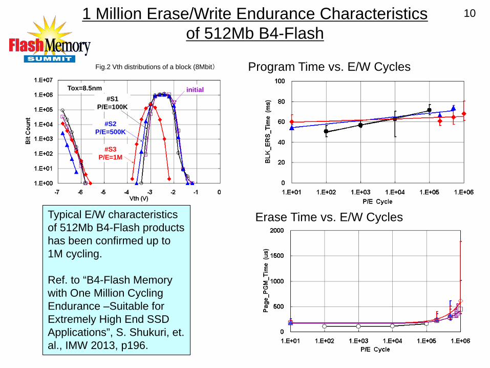
10 1 Million Erase/Write Endurance Characteristics of 512Mb B4-Flash
Program Time vs. E/W Cycles
Erase Time vs. E/W Cycles Typical E/W characteristics of 512Mb B4-Flash products has been confirmed up to 1M cycling. Ref. to “B4-Flash Memory with One Million Cycling Endurance –Suitable for Extremely High End SSD Applications”, S. Shukuri, et. al., IMW 2013, p196.
Tox=8.5nm initial
#S2P/E=500K
#S3P/E=1M
#S1P/E=100K
Fig.2 Vth distributions of a block (8Mbit)

11
-6
-5
-4
-3
-2
-1
Vte
min
, V
tpm
ax (
V)
init 100 101 102 103 104 105
Time (hr)
Vtemin
Vtpmax Tox=10.8nm
1k
10k
50k
100k 410k 1M E/W
4k
105
Num
ber o
f Bits
104
103
102
101
100
-8 -7 -6 -5 -4 -3 -2 -1 0 Vt (V)
-9
1hr
initial
30000hr
1003hr
10500hr
20080hr
Tox=10.8nm
-8 -7 -6 -5 -4 -3 -2 -1 0 Vt (V)
Tox=10.8nm
20140hr
30120hr
initial
1hr
135hr
15030hr
4000hr
105
Num
ber o
f Bits
104
103
102
101
100
Excellent Reliability Proven in very long term exam.
E/W=10k 250C Retention up to 3.4 years E/W=1M 150C Retention up to 3.4 years
150C Retention after E/W stress
one million E/W stress and 150C retention results show B4-Flash excellence in reliability .
130nm Process Examination
Each point denotes 32kbit statistics Each point denotes 32kbit statistics Each point denotes 32kbit statistics 3.4 Years
Defect Level 10y

B4-Flash succeeds to brakes through the limit of NOR Flash gate length
B4-Flash has achieved 512Mb Real Chip with 58nm gate length NOR
B4-Flash achieves the smallest NOR Cell for chips

Si-Capsule Controller LSI
Si-Capsule
B4-Flash
NAND
DRAM
sub- controller
GENUSION Package Solution for High Featured Storage Devices
- “real KGD” process using Burn-in and Full Function Test as Memory module -very wide bus I/Os with common dies - Si-Capsule can offer innovative devices for Storage Solution
Patented in US and Japan by GENUSION
14
B4-Flash embedded Storage for XIP operation in Hand-sets
15
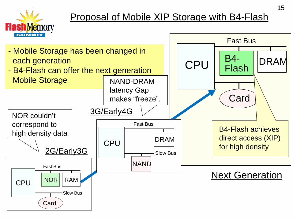
- Mobile Storage has been changed in each generation - B4-Flash can offer the next generation Mobile Storage
Proposal of Mobile XIP Storage with B4-Flash
Fast Bus
CPU NAND-DRAM latency Gap makes “freeze”.
NOR couldn’t correspond to high density data B4-Flash achieves
direct access (XIP) for high density
DRAM
Card
B4- Flash
Fast Bus
Slow Bus
CPU
Card
NOR RAM
Fast Bus
Slow Bus
CPU DRAM
NAND
2G/Early3G
3G/Early4G
Next Generation

16
Completely File Erasable SSD with B4-Flash

17
DeleteFile
A and C
Manage A Manage B Manage C
File A File B File CSecret Secret
NAND-StorageManage B
File A File B File CSecret Secret
NAND-StorageFile
RecoverS/W
Deleted Files can be Recovered !
File A File B File CSecret Secret
DeleteFile
A and C
Manage A Manage B Manage C
File A File B File CSecret Secret
B4 CE-StorageManage B
File B
B4 CE-StorageFile
RecoverS/W
Deleted Files CANNOT beRecovered !
File B
B4-Flash achieves Completely Erasable Data Storage thanks to its High Reliability.
Completely File Erasable Data Storage

18
Using B4-Flash instead
-B4-Flash achieves High Reliability
-Completely Erase of each File -Physical Erase Method
Completely File Erase can be done by B4-Flash
Conventional Storage Memory
Using NAND Flash
-No erase of the physical data due to less reliability of the device
-Only File Tag is changed -”Virtual Erase Method”
B4-Flash with high cycling endurance capability can execute file by file complete and physical data erase instead of “Virtual Erase”.
CE-File Memory (Completely Erasable)
Already in Production

19 Physics of Completely File Erase
Data programmed file state
(2) B4-Flash memory erase operation
(1) All “0” over-write to black out the data
Data”1” Data”0”
Data “1”
Data”0”
-B4-Flash, component of CE-File Memory, stores the data by electrical status of the memory cells, just the same as NAND. -B4-Flash can execute file by file data alternation, which NAND flash cannot. -B4-Flash can realize file by file complete erase.
File by file data erase
Internal operation
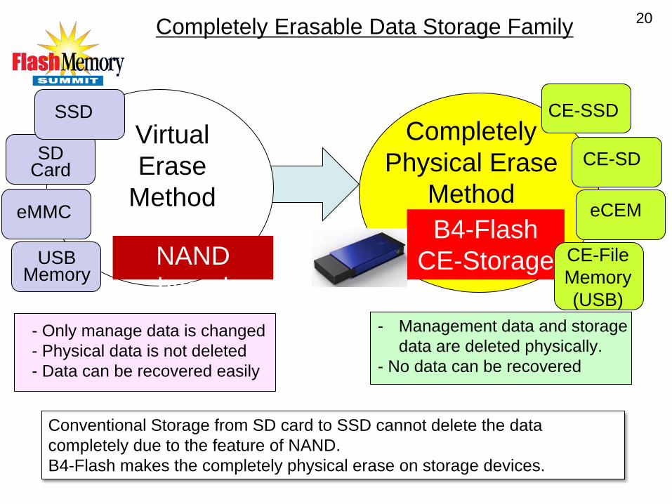
20 Completely Erasable Data Storage Family
Virtual Erase
Method
Completely Physical Erase
Method
NAND based
B4-Flash CE-Storage
SSD
SD Card
USB Memory
eMMC eCEM
CE-SD
CE-SSD
CE-File Memory (USB)
- Only manage data is changed - Physical data is not deleted - Data can be recovered easily
- Management data and storage data are deleted physically.
- No data can be recovered
Conventional Storage from SD card to SSD cannot delete the data completely due to the feature of NAND. B4-Flash makes the completely physical erase on storage devices.
21
100 years Data Retention SSD - 100yrs SSD -

22 100 year Data Retentive Storage with B4-Flash
HDD
B4-Flash
100 years Storage
- >100 years @RT - 20 years @ 125C
100 years SSD
100 years Mobile Storage
Media
B4-Flash can achieve 100 years retention storage device thanks to B4-Flash special feature.
Conventional SSD
Mechanical Issues Solved
Retention Issues Solved

23
Tier 0 SSD
for high-end featured Storage With B4-Flash
24
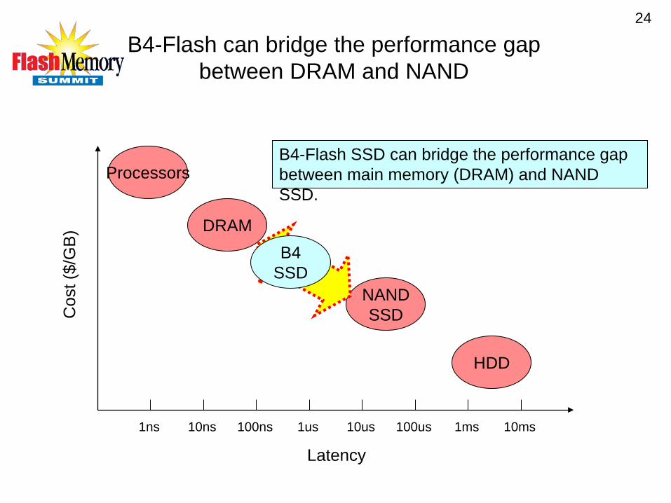
B4-Flash can bridge the performance gap between DRAM and NAND
Cos
t ($/
GB
)
Latency
1ns 10ns 100ns 1us 10us 100us 1ms 10ms
Processors
DRAM
NAND SSD
HDD
B4 SSD
B4-Flash SSD can bridge the performance gap between main memory (DRAM) and NAND SSD.
25
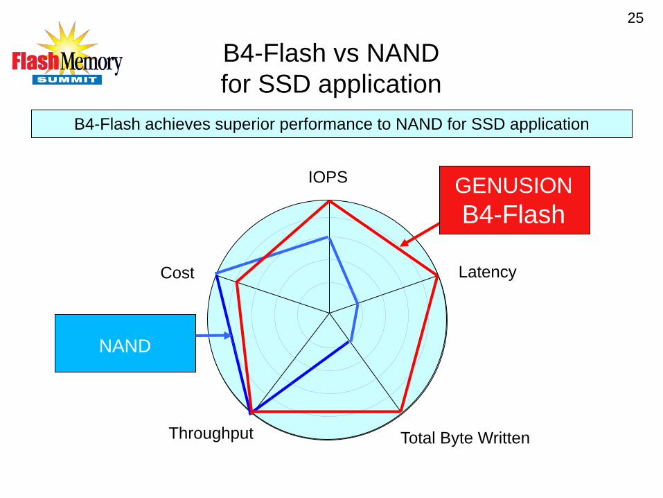
B4-Flash vs NAND for SSD application
B4-Flash achieves superior performance to NAND for SSD application
IOPS
Latency Cost
Throughput Total Byte Written
GENUSION B4-Flash
NAND
26
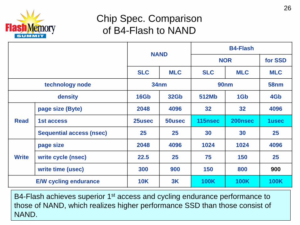
Chip Spec. Comparison of B4-Flash to NAND
B4-Flash achieves superior 1st access and cycling endurance performance to those of NAND, which realizes higher performance SSD than those consist of NAND.
NAND
B4-Flash
NOR for SSD
SLC MLC SLC MLC MLC
technology node 34nm 90nm 58nm
density 16Gb 32Gb 512Mb 1Gb 4Gb
Read
page size (Byte) 2048 4096 32 32 4096
1st access 25usec 50usec 115nsec 200nsec 1usec
Sequential access (nsec) 25 25 30 30 25
Write
page size 2048 4096 1024 1024 4096
write cycle (nsec) 22.5 25 75 150 25
write time (usec) 300 900 150 800 900
E/W cycling endurance 10K 3K 100K 100K 100K

27
Chip Spec. Comparison of B4-Flash to NAND for SSD application
B4-Flash achieves higher IOPS, faster latency and higher Total Bytes Written compared to those of NAND.
NAND
B4-Flash
NOR for SSD
SLC MLC SLC MLC MLC
technology node 34nm 90nm 58nm
density 16Gb 32Gb 512Mb 1Gb 4Gb
IOPS (4096B)
Read 7849 6562 13355 11660 9671
Write 2550 998 1566 305 998
Read/Write 5200 3780 7461 5983 5334
IOPS (512B)
Read 26455 15924 106838 93284 72464
Write 3210 1096 6460 1235 1096
Read/Write 14503 8461 56649 47259 36730
Through put (MB/s)
Read 40 40 66.7 66.7 40
Write 44.4 40 26.7 13.3 40
Read/Write 42.2 40 46.7 40 40
Latency 25usec 50usec 115nsec 200nsec 1usec
Total Bytes Written (TB) 20 12 6.4 12.8 50

28
◇ IOPs= + 0.5 Data transfer time (Read)
0.5 Data transfer time (Write)
○ NAND (MLC, 32Gb) <Data transfer time (Read)> 50us (1st acc.) + 25ns (seq. acc.) x 4096 (page size) = 152.4us < Data transfer time (Write)> 25ns (write cyc.) x 4096 (page size) + 900us (write time) = 1002.4us < IOPs > 3281 (Read) + 499 (Write) = 3780 ○ B4-Flash (MLC, 4Gb) <Data transfer time (Read)> 1us (1st acc.) + 25ns (seq. acc.) x 4096 (page size) = 103.4us < Data transfer time (Write)> 25ns (write cyc.) x 4096 (page size) + 900us (write time) = 1002.4us < IOPs > 4835 (Read) + 499 (Write) = 5334
Comparison of IOPs between B4-Flash and NAND (4096B, Read:Write=50:50)

29
128GB MLC B4-Flash SSD 150,000 IOPS, 13PBW latency=1usec – 100nsec
256GB SLC NAND SSD 100,000 IOPS, 2.6PBW latency=25usec
512GB MLC NAND SSD 60,000 IOPS, 1.5PBW latency=50usec
Tier 1
Tier 0
Tier 2
Tiered SSD example proposal by B4-Flash SSD and NAND SSD
IOPS TBW $/TBW ratio Latency Latency ratioHigh End HDD 400 infinity - msec 1
NAND-SSD 100k - 1milion 1.6PB - 16PB 1 several 10s usec 1/20B4-SSD 150k - 1.5milion 160PB 0.1 - 0.02 down to 100nsec 1/10000
Performance Comparison for 160GB High End HDD, NAND-SSD and B4-SSD
NAND SSD
B4 SSD

30
Summary
1.New Data Storage Arena for the high-end solution can
be created by B4-Flash with; - High Reliability - High Performance - High Density 2. New Data Storage features are ; - Completely File Erasable SSD - 100yrs Data Retention SSD - High performance SSD for high-end server Tier 0
Top Related