
![ECA [UandiStar.org].Unlocked](https://static.fdocuments.us/doc/165x107/55cf9005550346703ba264d6/eca-uandistarorgunlocked.jpg)


Languages
Pages
Legal

8/20/2019 At Mega 1281 Unlocked
http://slidepdf.com/reader/full/at-mega-1281-unlocked 1/446
Features High Performance, Low Power Atmel ® AVR ® 8-Bit Microcontroller
• Advanced RISC Architecture
– 135 Powerful Instructions – Most Single Clock Cycle Execution
– 32 × 8 General Purpose Working Registers
– Fully Static Operation
– Up to 16 MIPS Throughput at 16MHz
– On-Chip 2-cycle Multiplier• High Endurance Non-volatile Memory Segments
– 64K/128K/256KBytes of In-System Self-Programmable Flash
– 4Kbytes EEPROM
– 8Kbytes Internal SRAM
– Write/Erase Cycles:10,000 Flash/100,000 EEPROM
– Data retention: 20 years at 85°C/ 100 years at 25°C– Optional Boot Code Section with Independent Lock Bits
• In-System Programming by On-chip Boot Program
• True Read-While-Write Operation
– Programming Lock for Software Security
• Endurance: Up to 64Kbytes Optional External Memory Space
• Atmel ® QTouch ® library support
– Capacitive touch buttons, sliders and wheels
– QTouch and QMatrix® acquisition
– Up to 64 sense channels
• JTAG (IEEE std. 1149.1 compliant) Interface– Boundary-scan Capabilities According to the JTAG Standard
– Extensive On-chip Debug Support
– Programming of Flash, EEPROM, Fuses, and Lock Bits through the JTAG Interface
• Peripheral Features
– Two 8-bit Timer/Counters with Separate Prescaler and Compare Mode
– Four 16-bit Timer/Counter with Separate Prescaler, Compare- and Capture Mode
– Real Time Counter with Separate Oscillator
– Four 8-bit PWM Channels
– Six/Twelve PWM Channels with Programmable Resolution from 2 to 16 Bits
(ATmega1281/2561, ATmega640/1280/2560)
– Output Compare Modulator
– 8/16-channel, 10-bit ADC (ATmega1281/2561, ATmega640/1280/2560)
– Two/Four Programmable Serial USART (ATmega1281/2561, ATmega640/1280/2560)
– Master/Slave SPI Serial Interface
– Byte Oriented 2-wire Serial Interface
– Programmable Watchdog Timer with Separate On-chip Oscillator– On-chip Analog Comparator
– Interrupt and Wake-up on Pin Change
• Special Microcontroller Features
– Power-on Reset and Programmable Brown-out Detection
– Internal Calibrated Oscillator
– External and Internal Interrupt Sources
– Six Sleep Modes: Idle, ADC Noise Reduction, Power-save, Power-down, Standby,
and Extended Standby
• I/O and Packages
– 54/86 Programmable I/O Lines (ATmega1281/2561, ATmega640/1280/2560)
– 64-pad QFN/MLF, 64-lead TQFP (ATmega1281/2561)
– 100-lead TQFP, 100-ball CBGA (ATmega640/1280/2560)
– RoHS/Fully Green
• Temperature Range:
– -40°C to 85°C Industrial
• Ultra-Low Power Consumption– Active Mode: 1MHz, 1.8V: 500µA
– Power-down Mode: 0.1µA at 1.8V
• Speed Grade:
– ATmega640V/ATmega1280V/ATmega1281V:
• 0 - 4MHz @ 1.8V - 5.5V, 0 - 8MHz @ 2.7V - 5.5V
– ATmega2560V/ATmega2561V:
• 0 - 2MHz @ 1.8V - 5.5V, 0 - 8MHz @ 2.7V - 5.5V
– ATmega640/ATmega1280/ATmega1281:
• 0 - 8MHz @ 2.7V - 5.5V, 0 - 16MHz @ 4.5V - 5.5V
– ATmega2560/ATmega2561:
• 0 - 16MHz @ 4.5V - 5.5V
8-bit Atmel
Microcontroller
with
64K/128K/256K
Bytes In-System
Programmable
Flash
ATmega640/V
ATmega1280/V
ATmega1281/V
ATmega2560/VATmega2561/V
2549P–AVR–10/2012

8/20/2019 At Mega 1281 Unlocked
http://slidepdf.com/reader/full/at-mega-1281-unlocked 2/446
2
2549P–AVR–10/2012
ATmega640/1280/1281/2560/2561
1. Pin Configurations
Figure 1-1. TQFP-pinout ATmega640/1280/2560
GND
VCC
PA0(AD0)
PA1(AD1)
PA2(AD2)
PA3 (AD3)
PA4 (AD4)
PA5 (AD5)
PA6 (AD6)
PA7 (AD7)
PG2 (ALE)
A VCC
GND
AREF
PF0(ADC0)
PF1(ADC1)
PF2(ADC2)
PF3(ADC3)
PF4(ADC4/TCK)
PF5(ADC5/TMS)
PF6(ADC6/TDO)
PF7(ADC7/TDI)
100 99 98 97 96 95 94 93 92 91 90 89 88 87 86 85 84 83 82 81 80 79 78 77 76
1
2
3
4
5
6
7
8
9
10
11
12
13
14
15
16
17
18
19
20
21
22
23
24
25
75
74
73
72
71
70
69
68
67
66
65
64
63
62
61
60
59
58
57
56
55
54
53
52
51
26 28 29 3127 3630 32 35 3733 34 38 39 40 41 42 43 44 45 46 47 48 49 50
PK0(ADC
8 /PCINT16)
PK1(ADC9/PCINT17)
PK2(ADC10
/PCINT1
8 )
PK3(ADC11
/PCINT19)
PK4(ADC12
/PCINT20)
PK5(ADC13
/PCINT21)
PK6(ADC14
/PCINT22)
PK7(ADC15
/PCINT23)
(OC2B) PH6
(TOS
C2)PG3
(TOS
C1)PG4
RESET
(T4)PH7
(IC
P4)PL0
VCC
GND
XTAL2
XTAL1
PL6
PL7
GND
VCC
(OC0B) PG5
VCC
GND
(RXD2) PH0
(TXD2) PH1
(XCK2) PH2
(OC4A) PH3
(OC4B) PH4
(OC4C) PH5
(RXD0/PCINT8) PE0
(TXD0) PE1
(XCK0/AIN0) PE2
(OC3A/AIN1) PE3
(OC3B/INT4) PE4
(OC3C/INT5) PE5
(T3/INT6) PE6
(CLKO/ICP3/INT7) PE7
(SS/PCINT0) PB0
(SCK/PCINT1) PB1
(MOSI/PCINT2) PB2
(MISO/PCINT3) PB3
(OC2A/PCINT4) PB4
(OC1A/PCINT5) PB5
(OC1B/PCINT6) PB6
(OC0A/OC1C/ PCIN
T7)PB7
PC7 (A15)
PC6 (A14)
PC5 (A13)
PC4 (A12)
PC3 (A11)
PC2 (A10)
PC1 (A9)
PC0 (A8)
PG1 (RD)
PG0 (WR)
(TXD1/IN
T3)PD3
(IC
P1)PD4
(XC
K1)PD5
(T1)PD6
(T0)PD7
(SCL/IN
T0)PD0
(SDA/IN
T1)PD1
(RXD1/IN
T2)PD2
(IC
P5)PL1
(T5)PL2
(OC
5A)PL3
(OC
5B)PL4
PJ6 (PCINT15)
PJ5 (PCINT14)
PJ4 (PCINT13)
PJ3 (PCINT12)
PJ2 (XCK3/PCINT11)
PJ1 (TXD3/PCINT10)
PJ0 (RXD3/PCINT9)
PJ7
(OC
5C)PL5
INDEX CORNER

8/20/2019 At Mega 1281 Unlocked
http://slidepdf.com/reader/full/at-mega-1281-unlocked 3/446
3
2549P–AVR–10/2012
ATmega640/1280/1281/2560/2561
Figure 1-2. CBGA-pinout ATmega640/1280/2560
Note: The functions for each pin is the same as for the 100 pin packages shown in Figure 1-1 on page 2
A
B
C
D
E
F
G
H
J
K
1 2 3 4 5 6 7 8 9 10
A
B
C
D
E
F
G
H
J
K
10 9 8 7 6 5 4 3 2 1
Top view Bottom view
Table 1-1. CBGA-pinout ATmega640/1280/2560
1 2 3 4 5 6 7 8 9 10
A GND AREF PF0 PF2 PF5 PK0 PK3 PK6 GND VCC
B AVCC PG5 PF1 PF3 PF6 PK1 PK4 PK7 PA0 PA2
C PE2 PE0 PE1 PF4 PF7 PK2 PK5 PJ7 PA1 PA3
D PE3 PE4 PE5 PE6 PH2 PA4 PA5 PA6 PA7 PG2
E PE7 PH0 PH1 PH3 PH5 PJ6 PJ5 PJ4 PJ3 PJ2
F VCC PH4 PH6 PB0 PL4 PD1 PJ1 PJ0 PC7 GND
G GND PB1 PB2 PB5 PL2 PD0 PD5 PC5 PC6 VCC
H PB3 PB4 RESET PL1 PL3 PL7 PD4 PC4 PC3 PC2
J PH7 PG3 PB6 PL0 XTAL2 PL6 PD3 PC1 PC0 PG1
K PB7 PG4 VCC GND XTAL1 PL5 PD2 PD6 PD7 PG0

8/20/2019 At Mega 1281 Unlocked
http://slidepdf.com/reader/full/at-mega-1281-unlocked 4/446
4
2549P–AVR–10/2012
ATmega640/1280/1281/2560/2561
Figure 1-3. Pinout ATmega1281/2561
Note: The large center pad underneath the QFN /MLF package is made of metal and internally con-nected to GND. It should be soldered or glued to the board to ensure good mechanical stability. Ifthe center pad is left unconnected, the package might loosen from the board.
(RXD0/PCINT8 /PDI) PE0
(TXD0/PDO) PE1
(XCK0/AIN0) PE2
(OC3A/AIN1) PE3
(OC3B/INT4) PE4
(OC3C/INT5) PE5
(T3/INT6) PE6
(ICP3/CLKO/INT7) PE7
(SS/PCINT0) PB0
(OC0B) PG5
(SCK/PCINT1) PB1
(MOSI/PCINT2) PB2
(MISO/PCINT3) PB3
(OC2A/PCINT4) PB4
(OC1A/PCINT5) PB5
(OC1B/PCINT6) PB6
(OC0A/OC1C/PCINT7)PB7
(TOSC2)PG3
(TOSC1)PG4
RESET
VCC
GND
XTAL2
XTAL1
(SCL/INT0)PD0
(SDA/INT1)PD1
(RXD1/INT2)PD2
(TXD1/INT3)PD3
(ICP1)PD4
(XCK1)PD5
PA3 (AD3)
PA4 (AD4)
PA5 (AD5)
PA6 (AD6)
PA7 (AD7)
PG2 (ALE)
PC7 (A15)
PC6 (A14)
PC5 (A13)
PC4 (A12)
PC3 (A11)
PC2 (A10)
PC1 (A9)
PC0 (A8)
PG1 (RD)
PG0 (WR)
A V
CC
GN
D
AR
EF
PF
0(ADC0)
PF
1(ADC1)
PF
2(ADC2)
PF
3(ADC3)
PF
4(ADC4/TCK)
PF
5(ADC5/TMS)
PF
6(ADC6/TDO)
PF
7(ADC7/TDI)
GN
D
VC
C
PA
0(AD0)
PA
1(AD1)
PA
2(AD2)
(T1)PD6
(T0)PD7
INDEX CORNER
1
2
3
4
5
6
7
8
9
10
11
12
13
14
15
16
64
63
62
61
60
59
5 8
57
56
55
54
53
52
51
50
49
48
47
46
45
44
43
42
41
40
39
38
37
36
35
34
33
17
1 8
19
20
21
22
23
24
25
26
27
2 8
29
30
31
32
8/20/2019 At Mega 1281 Unlocked
http://slidepdf.com/reader/full/at-mega-1281-unlocked 5/446
5
2549P–AVR–10/2012
ATmega640/1280/1281/2560/2561
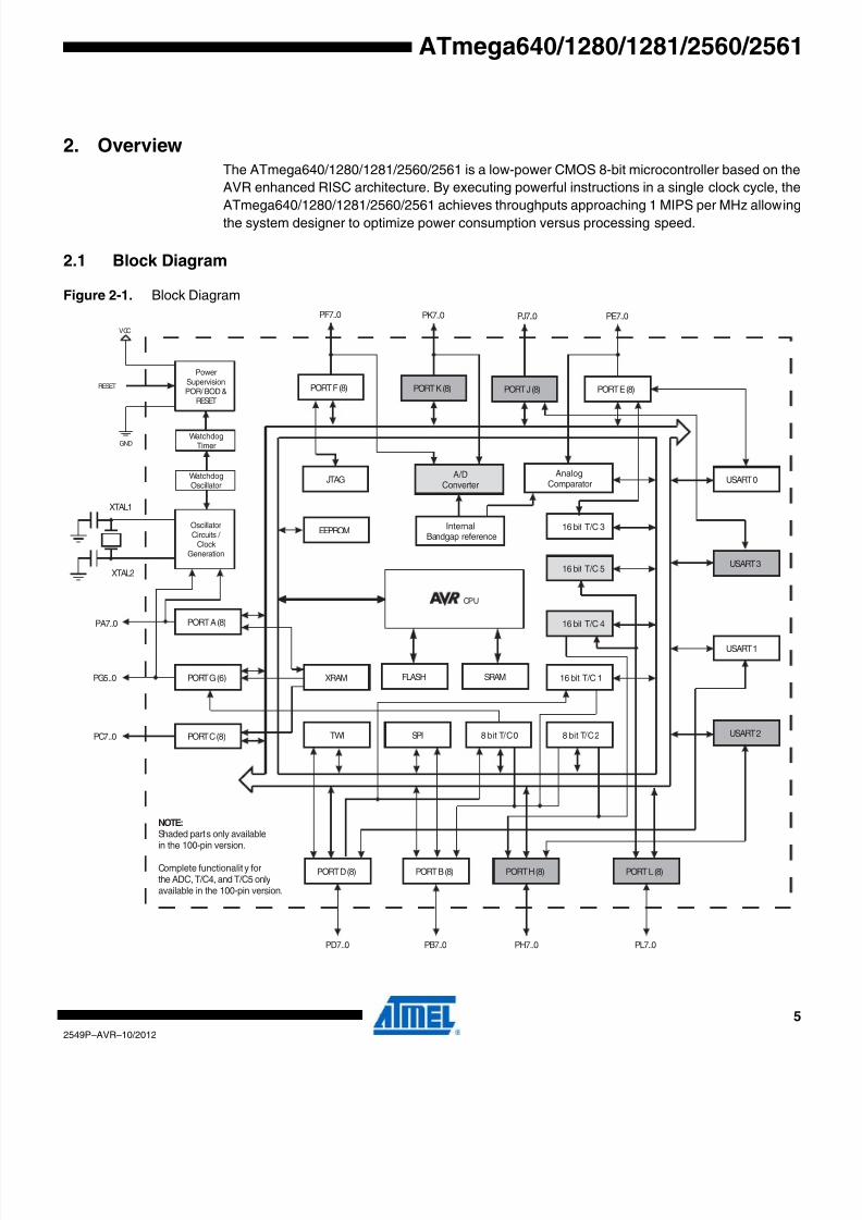
2. OverviewThe ATmega640/1280/1281/2560/2561 is a low-power CMOS 8-bit microcontroller based on the
AVR enhanced RISC architecture. By executing powerful instructions in a single clock cycle, the
ATmega640/1280/1281/2560/2561 achieves throughputs approaching 1 MIPS per MHz allowingthe system designer to optimize power consumption versus processing speed.
2.1 Block Diagram
Figure 2-1. Block Diagram
CPU
GND
VCC
RESET
PowerSupervisionPOR/ BOD &
RESET
WatchdogOscillator
WatchdogTimer
OscillatorCircuits /
ClockGeneration
XTAL1
XTAL2
PC7..0 PORT C (8)
PA7..0 PORT A (8)
PORT D (8)
PD7..0
PORT B (8)
PB7..0
PORT E (8)
PE7..0
PORT F (8)
PF7..0
PORT J (8)
PJ7..0
PG5..0 PORT G (6)
PORT H (8)
PH7..0
PORT K (8)
PK7..0
PORT L (8)
PL7..0
XRAM
TWI SPI
EEPROM
JTAG
8 bit T/C 0 8 bit T/C 2
16 bit T/C 1
16 bit T/C 3
SRAMFLASH
16 bit T/C 4
16 bit T/C 5
USART 2
USART 1
USART 0
InternalBandgap reference
AnalogComparator
A/DConverter
USART 3
NOTE:
Shaded parts only availablein the 100-pin version.
Complete functionalit y forthe ADC, T/C4, and T/C5 onlyavailable in the 100-pin version.
8/20/2019 At Mega 1281 Unlocked
http://slidepdf.com/reader/full/at-mega-1281-unlocked 6/446
6
2549P–AVR–10/2012
ATmega640/1280/1281/2560/2561
The Atmel ® AVR ® core combines a rich instruction set with 32 general purpose working regis
ters. All the 32 registers are directly connected to the Arithmetic Logic Unit (ALU), allowing two
independent registers to be accessed in one single instruction executed in one clock cycle. The
resulting architecture is more code efficient while achieving throughputs up to ten times faster
than conventional CISC microcontrollers.
The ATmega640/1280/1281/2560/2561 provides the following features: 64K/128K/256K bytes o
In-System Programmable Flash with Read-While-Write capabilities, 4Kbytes EEPROM, 8
Kbytes SRAM, 54/86 general purpose I/O lines, 32 general purpose working registers, Rea
Time Counter (RTC), six flexible Timer/Counters with compare modes and P WM, 4 USARTs, a
byte oriented 2-wire Serial Interface, a 16-channel, 10-bit ADC with optional differential input
stage with programmable gain, programmable Watchdog Timer with Internal Oscillator, an SP
serial port, IEEE ® std. 1149.1 compliant JTAG test interface, also used for accessing the On-
chip Debug system and programming and six software selectable power saving modes. The Idle
mode stops the CPU while allowing the SRAM, Timer/Counters, SPI port, and interrupt system
to continue functioning. The Power-down mode saves the register contents but freezes the
Oscillator, disabling all other chip functions until the next interrupt or Hardware Reset. In Power
save mode, the asynchronous timer continues to run, allowing the user to maintain a timer base
while the rest of the device is sleeping. The ADC Noise Reduction mode stops the CPU and alI/O modules except Asynchronous Timer and ADC, to minimize switching noise during ADC
conversions. In Standby mode, the Crystal/Resonator Oscillator is running while the rest of the
device is sleeping. This allows very fast start-up combined with low power consumption. In
Extended Standby mode, both the main Oscillator and the Asynchronous Timer continue to run
Atmel offers the QTouch ® library for embedding capacitive touch buttons, sliders and wheels
functionality into AVR microcontrollers. The patented charge-transfer signal acquisition
offersrobust sensing and includes fully debounced reporting of touch keys and includes Adjacen
KeySuppression ® (AKS™) technology for unambiguous detection of key events. The easy-to-use
QTouch Suite toolchain allows you to explore, develop and debug your own touch applications.
The device is manufactured using Atmel’s high-density nonvolatile memory technology. The On-
chip ISP Flash allows the program memory to be reprogrammed in-system through an SPI seriainterface, by a conventional nonvolatile memory programmer, or by an On-chip Boot program
running on the AVR core. The boot program can use any interface to download the application
program in the application Flash memory. Software in the Boot Flash section will continue to run
while the Application Flash section is updated, providing true Read-While-Write operation. By
combining an 8-bit RISC CPU with In-System Self-Programmable Flash on a monolithic chip
the Atmel ATmega640/1280/1281/2560/2561 is a powerful microcontroller that provides a highly
flexible and cost effective solution to many embedded control applications.
The ATmega640/1280/1281/2560/2561 AVR is supported with a full suite of program and sys-
tem deve lopment too ls inc lud ing : C compi le rs , macro assemblers , p rogram
debugger/simulators, in-circuit emulators, and evaluation kits.

8/20/2019 At Mega 1281 Unlocked
http://slidepdf.com/reader/full/at-mega-1281-unlocked 7/446
7
2549P–AVR–10/2012
ATmega640/1280/1281/2560/2561
2.2 Comparison Between ATmega1281/2561 and ATmega640/1280/2560
Each device in the ATmega640/1280/1281/2560/2561 family differs only in memory size and
number of pins. Table 2-1 summarizes the different configurations for the six devices.
2.3 Pin Descriptions
2.3.1 VCC
Digital supply voltage.
2.3.2 GND
Ground.
2.3.3 Port A (PA7..PA0)
Port A is an 8-bit bi-directional I/O port with internal pull-up resistors (selected for each bit). The
Port A output buffers have symmetrical drive characteristics with both high sink and source
capability. As inputs, Port A pins that are externally pulled low will source current if the pull-up
resistors are activated. The Port A pins are tri-stated when a reset condition becomes active
even if the clock is not running.
Por t A a lso serves the func t ions o f var ious spec ia l f ea tures o f the
ATmega640/1280/1281/2560/2561 as listed on page 78.
2.3.4 Port B (PB7..PB0)
Port B is an 8-bit bi-directional I/O port with internal pull-up resistors (selected for each bit). The
Port B output buffers have symmetrical drive characteristics with both high sink and source
capability. As inputs, Port B pins that are externally pulled low will source current if the pull-up
resistors are activated. The Port B pins are tri-stated when a reset condition becomes active
even if the clock is not running.
Port B has better driving capabilities than the other ports.
Por t B a lso serves the func t ions o f var ious spec ia l f ea tures o f the
ATmega640/1280/1281/2560/2561 as listed on page 79.
2.3.5 Port C (PC7..PC0)
Port C is an 8-bit bi-directional I/O port with internal pull-up resistors (selected for each bit). The
Port C output buffers have symmetrical drive characteristics with both high sink and source
capability. As inputs, Port C pins that are externally pulled low will source current if the pull-up
Table 2-1. Configuration Summary
Device Flash EEPROM RAM
General
Purpose I/O pins
16 bits resolution
PWM channels
Serial
USARTs
ADC
Channels
ATmega640 64KB 4KB 8KB 86 12 4 16
ATmega1280 128KB 4KB 8KB 86 12 4 16
ATmega1281 128KB 4KB 8KB 54 6 2 8
ATmega2560 256KB 4KB 8KB 86 12 4 16
ATmega2561 256KB 4KB 8KB 54 6 2 8

8/20/2019 At Mega 1281 Unlocked
http://slidepdf.com/reader/full/at-mega-1281-unlocked 8/446
8
2549P–AVR–10/2012
ATmega640/1280/1281/2560/2561
resistors are activated. The Port C pins are tri-stated when a reset condition becomes active
even if the clock is not running.
Port C also serves the functions of special features of the ATmega640/1280/1281/2560/2561 as
listed on page 82.
2.3.6 Port D (PD7..PD0)
Port D is an 8-bit bi-directional I/O port with internal pull-up resistors (selected for each bit). The
Port D output buffers have symmetrical drive characteristics with both high sink and source
capability. As inputs, Port D pins that are externally pulled low will source current if the pull-up
resistors are activated. The Port D pins are tri-stated when a reset condition becomes active
even if the clock is not running.
Por t D a lso serves the func t ions o f var ious spec ia l f ea tures o f the
ATmega640/1280/1281/2560/2561 as listed on page 83.
2.3.7 Port E (PE7..PE0)
Port E is an 8-bit bi-directional I/O port with internal pull-up resistors (selected for each bit). The
Port E output buffers have symmetrical drive characteristics with both high sink and source
capability. As inputs, Port E pins that are externally pulled low will source current if the pull-upresistors are activated. The Port E pins are tri-stated when a reset condition becomes active
even if the clock is not running.
Por t E a lso serves the func t ions o f var ious spec ia l f ea tures o f the
ATmega640/1280/1281/2560/2561 as listed on page 86.
2.3.8 Port F (PF7..PF0)
Port F serves as analog inputs to the A/D Converter.
Port F also serves as an 8-bit bi-directional I/O port, if the A/D Converter is not used. Port pins
can provide internal pull-up resistors (selected for each bit). The Port F output buffers have sym
metrical drive characteristics with both high sink and source capability. As inputs, Port F pins
that are externally pulled low will source current if the pull-up resistors are activated. The Port F
pins are tri-stated when a reset condition becomes active, even if the clock is not running. If the
JTAG interface is enabled, the pull-up resistors on pins PF7(TDI), PF5(TMS), and PF4(TCK) wil
be activated even if a reset occurs.
Port F also serves the functions of the JTAG interface.
2.3.9 Port G (PG5..PG0)
Port G is a 6-bit I/O port with internal pull-up resistors (selected for each bit). The Port G output
buffers have symmetrical drive characteristics with both high sink and source capability. As
inputs, Port G pins that are externally pulled low will source current if the pull-up resistors are
activated. The Port G pins are tri-stated when a reset condition becomes active, even if the clock
is not running.
Por t G a lso serves the func t ions o f var ious spec ia l f ea tures o f the
ATmega640/1280/1281/2560/2561 as listed on page 90.
2.3.10 Port H (PH7..PH0)
Port H is a 8-bit bi-directional I/O port with internal pull-up resistors (selected for each bit). The
Port H output buffers have symmetrical drive characteristics with both high sink and source
capability. As inputs, Port H pins that are externally pulled low will source current if the pull-up
8/20/2019 At Mega 1281 Unlocked
http://slidepdf.com/reader/full/at-mega-1281-unlocked 9/446
9
2549P–AVR–10/2012
ATmega640/1280/1281/2560/2561
resistors are activated. The Port H pins are tri-stated when a reset condition becomes active
even if the clock is not running.
Port H also serves the functions of various special features of the ATmega640/1280/2560 as
listed on page 92.
2.3.11 Port J (PJ7..PJ0)
Port J is a 8-bit bi-directional I/O port with internal pull-up resistors (selected for each bit). The
Port J output buffers have symmetrical drive characteristics with both high sink and source capa-
bility. As inputs, Port J pins that are externally pulled low will source current if the pull-up
resistors are activated. The Port J pins are tri-stated when a reset condition becomes active
even if the clock is not running.
Port J also serves the functions of various special features of the ATmega640/1280/2560 as
listed on page 94.
2.3.12 Port K (PK7..PK0)
Port K serves as analog inputs to the A/D Converter.
Port K is a 8-bit bi-directional I/O port with internal pull-up resistors (selected for each bit). ThePort K output buffers have symmetrical drive characteristics with both high sink and source
capability. As inputs, Port K pins that are externally pulled low will source current if the pull-up
resistors are activated. The Port K pins are tri-stated when a reset condition becomes active
even if the clock is not running.
Port K also serves the functions of various special features of the ATmega640/1280/2560 as
listed on page 96.
2.3.13 Port L (PL7..PL0)
Port L is a 8-bit bi-directional I/O port with internal pull-up resistors (selected for each bit). The
Port L output buffers have symmetrical drive characteristics with both high sink and source
capability. As inputs, Port L pins that are externally pulled low will source current if the pull-up
resistors are activated. The Port L pins are tri-stated when a reset condition becomes active
even if the clock is not running.
Port L also serves the functions of various special features of the ATmega640/1280/2560 as
listed on page 98.
2.3.14 RESET
Reset input. A low level on this pin for longer than the minimum pulse length will generate a
reset, even if the clock is not running. The minimum pulse length is given in “System and Rese
Characteristics” on page 372. Shorter pulses are not guaranteed to generate a reset.
2.3.15 XTAL1
Input to the inverting Oscillator amplifier and input to the internal clock operating circuit.
2.3.16 XTAL2
Output from the inverting Oscillator amplifier.

8/20/2019 At Mega 1281 Unlocked
http://slidepdf.com/reader/full/at-mega-1281-unlocked 10/446
10
2549P–AVR–10/2012
ATmega640/1280/1281/2560/2561
2.3.17 AVCC
AVCC is the supply voltage pin for Port F and the A/D Converter. It should be externally con
nected to VCC, even if the ADC is not used. If the ADC is used, it should be connected to VCC
through a low-pass filter.
2.3.18 AREF
This is the analog reference pin for the A/D Converter.

8/20/2019 At Mega 1281 Unlocked
http://slidepdf.com/reader/full/at-mega-1281-unlocked 11/446
11
2549P–AVR–10/2012
ATmega640/1280/1281/2560/2561
3. ResourcesA comprehensive set of development tools and application notes, and datasheets are available
for download on http://www.atmel.com/avr.
4. About Code ExamplesThis documentation contains simple code examples that briefly show how to use various parts o
the device. Be aware that not all C compiler vendors include bit definitions in the header files
and interrupt handling in C is compiler dependent. Please confirm with the C compiler documen
tation for more details.
These code examples assume that the part specific header file is included before compilation.
For I/O registers located in extended I/O map, "IN", "OUT", "SBIS", "SBIC", "CBI", and "SBI"
instructions must be replaced with instructions that allow access to extended I/O. Typically
"LDS" and "STS" combined with "SBRS", "SBRC", "SBR", and "CBR".
5. Data RetentionReliability Qualification results show that the projected data retention failure rate is much less
than 1 ppm over 20 years at 85°C or 100 years at 25°C.
6. Capacitive touch sensingThe Atmel ® QTouch ® Library provides a simple to use solution to realize touch sensitive inter
faces on most Atmel AVR ® microcontrollers. The QTouch Library includes support for the
QTouch and QMatrix ® acquisition methods.
Touch sensing can be added to any application by linking the appropriate Atmel QTouch Library
for the AVR Microcontroller. This is done by using a simple set of APIs to define the touch chan-
nels and sensors, and then calling the touch sensing API’s to retrieve the channel information
and determine the touch sensor states.
The QTouch Library is FREE and downloadable from the Atmel website at the following location
www.atmel.com/qtouchlibrary. For implementation details and other information, refer to the
Atmel QTouch Library User Guide - also available for download from the Atmel website.

8/20/2019 At Mega 1281 Unlocked
http://slidepdf.com/reader/full/at-mega-1281-unlocked 12/446
12
2549P–AVR–10/2012
ATmega640/1280/1281/2560/2561
7. AVR CPU Core
7.1 Introduction
This section discusses the AVR core architecture in general. The main function of the CPU core
is to ensure correct program execution. The CPU must therefore be able to access memories
perform calculations, control peripherals, and handle interrupts.
7.2 Architectural Overview
Figure 7-1. Block Diagram of the AVR Architecture
In order to maximize performance and parallelism, the AVR uses a Harvard architecture – with
separate memories and buses for program and data. Instructions in the program memory are
executed with a single level pipelining. While one instruction is being executed, the next instruc-
tion is pre-fetched from the program memory. This concept enables instructions to be executed
in every clock cycle. The program memory is In-System Reprogrammable Flash memory.
FlashProgramMemory
InstructionRegister
InstructionDecoder
ProgramCounter
Control Lines
32 x 8GeneralPurpose
Registers
ALU
Statusand Control
I/O Lines
EEPROM
Data Bus 8-bit
DataSRAM
DirectAddressing
I
ndirectAddressing
InterruptUnit
SPIUnit
WatchdogTimer
AnalogComparator
I/O Module 2
I/O Module1
I/O Module n

8/20/2019 At Mega 1281 Unlocked
http://slidepdf.com/reader/full/at-mega-1281-unlocked 13/446
13
2549P–AVR–10/2012
ATmega640/1280/1281/2560/2561
The fast-access Register File contains 32 × 8-bit general purpose working registers with a single
clock cycle access time. This allows single-cycle Arithmetic Logic Unit (ALU) operation. In a typ
ical ALU operation, two operands are output from the Register File, the operation is executed,
and the result is stored back in the Register File – in one clock cycle.
Six of the 32 registers can be used as three 16-bit indirect address register pointers for Data
Space addressing – enabling efficient address calculations. One of the these address pointers
can also be used as an address pointer for look up tables in Flash program memory. These
added function registers are the 16-bit X-, Y-, and Z-register, described later in this section.
The ALU supports arithmetic and logic operations between registers or between a constant and
a register. Single register operations can also be executed in the ALU. After an arithmetic opera-
tion, the Status Register is updated to reflect information about the result of the operation.
Program flow is provided by conditional and unconditional jump and call instructions, able to
directly address the whole address space. Most AVR instructions have a single 16-bit word for
mat. Every program memory address contains a 16-bit or 32-bit instruction.
Program Flash memory space is divided in two sections, the Boot Program section and the
Application Program section. Both sections have dedicated Lock bits for write and read/write
protection. The SPM instruction that writes into the Application Flash memory section musreside in the Boot Program section.
During interrupts and subroutine calls, the return address Program Counter (PC) is stored on the
Stack. The Stack is effectively allocated in the general data SRAM, and consequently the Stack
size is only limited by the total SRAM size and the usage of the SRAM. All user programs mus
initialize the SP in the Reset routine (before subroutines or interrupts are executed). The Stack
Pointer (SP) is read/write accessible in the I/O space. The data SRAM can easily be accessed
through the five different addressing modes supported in the AVR architecture.
The memory spaces in the AVR architecture are all linear and regular memory maps.
A flexible interrupt module has its control registers in the I/O space with an additional Globa
Interrupt Enable bit in the Status Register. All interrupts have a separate Interrupt Vector in theInterrupt Vector table. The interrupts have priority in accordance with their Interrupt Vector posi-
tion. The lower the Interrupt Vector address, the higher the priority.
The I/O memory space contains 64 addresses for CPU peripheral functions as Control Regis-
ters, SPI, and other I/O functions. The I/O Memory can be accessed directly, or as the Data
Space locations following those of the Register File, 0x20 - 0x5F. In addit ion, the
ATmega640/1280/1281/2560/2561 has Extended I/O space from 0x60 - 0x1FF in SRAM where
only the ST/STS/STD and LD/LDS/LDD instructions can be used.
7.3 ALU – Arithmetic Logic Unit
The high-performance AVR ALU operates in direct connection with all the 32 general purpose
working registers. Within a single clock cycle, arithmetic operations between general purposeregisters or between a register and an immediate are executed. The ALU operations are divided
into three main categories – arithmetic, logical, and bit-functions. Some implementations of the
architecture also provide a powerful multiplier supporting both signed/unsigned multiplication
and fractional format. See the “Instruction Set Summary” on page 416 for a detailed description
8/20/2019 At Mega 1281 Unlocked
http://slidepdf.com/reader/full/at-mega-1281-unlocked 14/446
14
2549P–AVR–10/2012
ATmega640/1280/1281/2560/2561
7.4 Status Register
The Status Register contains information about the result of the most recently executed arithme
tic instruction. This information can be used for altering program flow in order to perform
conditional operations. Note that the Status Register is updated after all ALU operations, as
specified in the “Instruction Set Summary” on page 416. This will in many cases remove the
need for using the dedicated compare instructions, resulting in faster and more compact code.
The Status Register is not automatically stored when entering an interrupt routine and restored
when returning from an interrupt. This must be handled by software.
7.4.1 SREG – AVR Status Register
The AVR Status Register – SREG – is defined as:
• Bit 7 – I: Global Interrupt Enable
The Global Interrupt Enable bit must be set for the interrupts to be enabled. The individual inter-rupt enable control is then performed in separate control registers. If the Global Interrupt Enable
Register is cleared, none of the interrupts are enabled independent of the individual interrup
enable settings. The I-bit is cleared by hardware after an interrupt has occurred, and is set by
the RETI instruction to enable subsequent interrupts. The I-bit can also be set and cleared by
the application with the SEI and CLI instructions, as described in the “Instruction Set Summary”
on page 416.
• Bit 6 – T: Bit Copy Storage
The Bit Copy instructions BLD (Bit LoaD) and BST (Bit STore) use the T-bit as source or desti-
nation for the operated bit. A bit from a register in the Register File can be copied into T by the
BST instruction, and a bit in T can be copied into a bit in a register in the Register File by the
BLD instruction.
• Bit 5 – H: Half Carry Flag
The Half Carry Flag H indicates a Half Carry in some arithmetic operations. Half Carry Is usefu
in BCD arithmetic. See the “Instruction Set Summary” on page 416 for detailed information.
• Bit 4 – S: Sign Bit, S = N ⊕ V
The S-bit is always an exclusive or between the Negative Flag N and the Two’s Complemen
Overflow Flag V. See the “Instruction Set Summary” on page 416 for detailed information.
• Bit 3 – V: Two’s Complement Overflow Flag
The Two’s Complement Overflow Flag V supports two’s complement arithmetics. See the“Instruction Set Summary” on page 416 for detailed information.
• Bit 2 – N: Negative Flag
The Negative Flag N indicates a negative result in an arithmetic or logic operation. See the
“Instruction Set Summary” on page 416 for detailed information.
Bit 7 6 5 4 3 2 1 0
0x3F (0x5F) I T H S V N Z C SREG
Read/ Write R/ W R/ W R/ W R/ W R/ W R/ W R/ W R/ W
Initial Value 0 0 0 0 0 0 0 0

8/20/2019 At Mega 1281 Unlocked
http://slidepdf.com/reader/full/at-mega-1281-unlocked 15/446
15
2549P–AVR–10/2012
ATmega640/1280/1281/2560/2561
• Bit 1 – Z: Zero Flag
The Zero Flag Z indicates a zero result in an arithmetic or logic operation. See the “Instruction
Set Summary” on page 416 for detailed information.
• Bit 0 – C: Carry Flag
The Carry Flag C indicates a carry in an arithmetic or logic operation. See the “Instruction Se
Summary” on page 416 for detailed information.
7.5 General Purpose Register File
The Register File is optimized for the AVR Enhanced RISC instruction set. In order to achieve
the required performance and flexibility, the following input/output schemes are supported by the
Register File:
• One 8-bit output operand and one 8-bit result input
• Two 8-bit output operands and one 8-bit result input
• Two 8-bit output operands and one 16-bit result input
• One 16-bit output operand and one 16-bit result input
Figure 7-2 shows the structure of the 32 general purpose working registers in the CPU.
Figure 7-2. AVR CPU General Purpose Working Registers
Most of the instructions operating on the Register File have direct access to all registers, and
most of them are single cycle instructions.
As shown in Figure 7-2, each register is also assigned a data memory address, mapping them
directly into the first 32 locations of the user Data Space. Although not being physically imple-
mented as SRAM locations, this memory organization provides great flexibility in access of the
registers, as the X-, Y- and Z-pointer registers can be set to index any register in the file.
7.5.1 The X-register, Y-register, and Z-register
The registers R26..R31 have some added functions to their general purpose usage. These reg
isters are 16-bit address pointers for indirect addressing of the data space. The three indirec
address registers X, Y, and Z are defined as described in Figure 7-3 on page 16.
7 0 Addr.
R0 0x00
R1 0x01
R2 0x02
…
R13 0x0D
General R14 0x0E
Purpose R15 0x0F
Working R16 0x10
Registers R17 0x11
…
R26 0x1A X-register Low Byte
R27 0x1B X-register High Byte
R28 0x1C Y-register Low Byte
R29 0x1D Y-register High Byte
R30 0x1E Z-register Low Byte
R31 0x1F Z-register High Byte
8/20/2019 At Mega 1281 Unlocked
http://slidepdf.com/reader/full/at-mega-1281-unlocked 16/446
16
2549P–AVR–10/2012
ATmega640/1280/1281/2560/2561
Figure 7-3. The X-, Y-, and Z-registers
In the different addressing modes these address registers have functions as fixed displacement
automatic increment, and automatic decrement (see the “Instruction Set Summary” on page 416
for details).
7.6 Stack Pointer
The Stack is mainly used for storing temporary data, for storing local variables and for storing
return addresses after interrupts and subroutine calls. The Stack Pointer Register always points
to the top of the Stack. Note that the Stack is implemented as growing from higher memory loca
tions to lower memory locations. This implies that a Stack PUSH command decreases the Stack
Pointer.
The Stack Pointer points to the data SRAM Stack area where the Subroutine and Interrup
Stacks are located. This Stack space in the data SRAM must be defined by the program before
any subroutine calls are executed or interrupts are enabled. The Stack Pointer must be set to
point above 0x0200. The initial value of the stack pointer is the last address of the interna
SRAM. The Stack Pointer is decremented by one when data is pushed onto the Stack with the
PUSH instruction, and it is decremented by two for ATmega640/1280/1281 and three for
ATmega2560/2561 when the return address is pushed onto the Stack with subroutine call o
interrupt. The Stack Pointer is incremented by one when data is popped from the Stack with thePOP instruction, and it is incremented by two for ATmega640/1280/1281 and three for
ATmega2560/2561 when data is popped from the Stack with return from subroutine RET or
return from interrupt RETI.
The AVR Stack Pointer is implemented as two 8-bit registers in the I/O space. The number of
bits actually used is implementation dependent. Note that the data space in some implementa-
tions of the AVR architecture is so small that only SPL is needed. In this case, the SPH Registe
will not be present.
15 XH XL 0
X-register 7 0 7 0
R27 (0x1B) R26 (0x1A)
15 YH YL 0Y-register 7 0 7 0
R29 (0x1D) R28 (0x1C)
15 ZH ZL 0
Z-register 7 0 7 0
R31 (0x1F) R30 (0x1E)
Bit 15 14 13 12 11 10 9 8
0x3E (0x5E) SP15 SP14 SP13 SP12 SP11 SP10 SP9 SP8 SPH
0x3D (0x5D) SP7 SP6 SP5 SP4 SP3 SP2 SP1 SP0 SPL
7 6 5 4 3 2 1 0
Read/ Write R/ W R/ W R/ W R/ W R/ W R/ W R/ W R/ W
R/ W R/ W R/ W R/ W R/ W R/ W R/ W R/ W
Initial Value 0 0 1 0 0 0 0 1
1 1 1 1 1 1 1 1
8/20/2019 At Mega 1281 Unlocked
http://slidepdf.com/reader/full/at-mega-1281-unlocked 17/446
17
2549P–AVR–10/2012
ATmega640/1280/1281/2560/2561
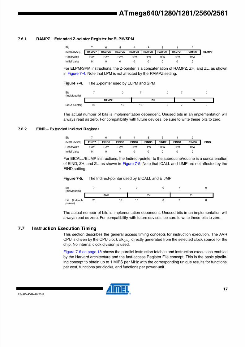
7.6.1 RAMPZ – Extended Z-pointer Register for ELPM/SPM
For ELPM/SPM instructions, the Z-pointer is a concatenation of RAMPZ, ZH, and ZL, as shown
in Figure 7-4. Note that LPM is not affected by the RAMPZ setting.
Figure 7-4. The Z-pointer used by ELPM and SPM
The actual number of bits is implementation dependent. Unused bits in an implementation wil
always read as zero. For compatibility with future devices, be sure to write these bits to zero.
7.6.2 EIND – Extended Indirect Register
For EICALL/EIJMP instructions, the Indirect-pointer to the subroutine/routine is a concatenation
of EIND, ZH, and ZL, as shown in Figure 7-5. Note that ICALL and IJMP are not affected by the
EIND setting.
Figure 7-5. The Indirect-pointer used by EICALL and EIJMP
The actual number of bits is implementation dependent. Unused bits in an implementation wil
always read as zero. For compatibility with future devices, be sure to write these bits to zero.
7.7 Instruction Execution Timing
This section describes the general access timing concepts for instruction execution. The AVR
CPU is driven by the CPU clock clkCPU, directly generated from the selected clock source for the
chip. No internal clock division is used.
Figure 7-6 on page 18 shows the parallel instruction fetches and instruction executions enabled
by the Harvard architecture and the fast-access Register File concept. This is the basic pipelin
ing concept to obtain up to 1 MIPS per MHz with the corresponding unique results for functions
per cost, functions per clocks, and functions per power-unit.
Bit 7 6 5 4 3 2 1 0
0x3B (0x5B) RAMPZ7 RAMPZ6 RAMPZ5 RAMPZ4 RAMPZ3 RAMPZ2 RAMPZ1 RAMPZ0 RAMPZ
Read/ Write R/ W R/ W R/ W R/ W R/ W R/ W R/ W R/ W
Initial Value 0 0 0 0 0 0 0 0
Bit(Individually)
7 0 7 0 7 0
RAMPZ ZH ZL
Bit (Z-pointer) 23 16 15 8 7 0
Bit 7 6 5 4 3 2 1 0
0x3C (0x5C) EIND7 EIND6 EIND5 EIND4 EIND3 EIND2 EIND1 EIND0 EIND
Read/ Write R/ W R/ W R/ W R/ W R/ W R/ W R/ W R/ W
Initial Value 0 0 0 0 0 0 0 0
Bit(Individually)
7 0 7 0 7 0
EIND ZH ZL
Bit (Indirect-pointer)
23 16 15 8 7 0

8/20/2019 At Mega 1281 Unlocked
http://slidepdf.com/reader/full/at-mega-1281-unlocked 18/446
18
2549P–AVR–10/2012
ATmega640/1280/1281/2560/2561
Figure 7-6. The Parallel Instruction Fetches and Instruction Executions
Figure 7-7 shows the internal timing concept for the Register File. In a single clock cycle an ALU
operation using two register operands is executed, and the result is stored back to the destina-
tion register.
Figure 7-7. Single Cycle ALU Operation
7.8 Reset and Interrupt Handling
The AVR provides several different interrupt sources. These interrupts and the separate Reset
Vector each have a separate program vector in the program memory space. All interrupts are
assigned individual enable bits which must be written logic one together with the Global Interrup
Enable bit in the Status Register in order to enable the interrupt. Depending on the Program
Counter value, interrupts may be automatically disabled when Boot Lock bits BLB02 or BLB12
are programmed. This feature improves software security. See the section “Memory Program
ming” on page 335 for details.
The lowest addresses in the program memory space are by default defined as the Reset and
Interrupt Vectors. The complete list of vectors is shown in “Interrupts” on page 105. The list also
determines the priority levels of the different interrupts. The lower the address the higher is the
priority level. RESET has the highest priority, and next is INT0 – the External Interrupt Reques
0. The Interrupt Vectors can be moved to the start of the Boot Flash section by setting the IVSELbit in the MCU Control Register (MCUCR). Refer to “Interrupts” on page 105 for more informa-
tion. The Reset Vector can also be moved to the start of the Boot Flash section by programming
the BOOTRST Fuse, see “Memory Programming” on page 335.
When an interrupt occurs, the Global Interrupt Enable I-bit is cleared and all interrupts are dis
abled. The user software can write logic one to the I-bit to enable nested interrupts. All enabled
interrupts can then interrupt the current interrupt routine. The I-bit is automatically set when a
Return from Interrupt instruction – RETI – is executed.
clk
1st Instruction Fetch
1st Instruction Execute2nd Instruction Fetch
2nd Instruction Execute3rd Instruction Fetch
3rd Instruction Execute4th Instruction Fetch
T1 T2 T3 T4
CPU
Total Execution Time
Register Operands Fetch
ALU Operation Execute
Result Write Back
T1 T2 T3 T4
clkCPU

8/20/2019 At Mega 1281 Unlocked
http://slidepdf.com/reader/full/at-mega-1281-unlocked 19/446
19
2549P–AVR–10/2012
ATmega640/1280/1281/2560/2561
There are basically two types of interrupts. The first type is triggered by an event that sets the
Interrupt Flag. For these interrupts, the Program Counter is vectored to the actual Interrupt Vec
tor in order to execute the interrupt handling routine, and hardware clears the corresponding
Interrupt Flag. Interrupt Flags can also be cleared by writing a logic one to the flag bit position(s)
to be cleared. If an interrupt condition occurs while the corresponding interrupt enable bit is
cleared, the Interrupt Flag will be set and remembered until the interrupt is enabled, or the flag is
cleared by software. Similarly, if one or more interrupt conditions occur while the Global InterrupEnable bit is cleared, the corresponding Interrupt Flag(s) will be set and remembered until the
Global Interrupt Enable bit is set, and will then be executed by order of priority.
The second type of interrupts will trigger as long as the interrupt condition is present. These
interrupts do not necessarily have Interrupt Flags. If the interrupt condition disappears before the
interrupt is enabled, the interrupt will not be triggered.
When the AVR exits from an interrupt, it will always return to the main program and execute one
more instruction before any pending interrupt is served.
Note that the Status Register is not automatically stored when entering an interrupt routine, nor
restored when returning from an interrupt routine. This must be handled by software.
When using the CLI instruction to disable interrupts, the interrupts will be immediately disabledNo interrupt will be executed after the CLI instruction, even if it occurs simultaneously with the
CLI instruction. The following example shows how this can be used to avoid interrupts during the
timed EEPROM write sequence.
When using the SEI instruction to enable interrupts, the instruction following SEI will be exe-
cuted before any pending interrupts, as shown in this example.
Assembly Code Example
in r16, SREG ; store SREG value
cli ; disable interrupts during timed sequence
sbi EECR, EEMPE ; start EEPROM write
sbi EECR, EEPE
out SREG, r16 ; restore SREG value (I-bit)
C Code Example
char cSREG;
cSREG = SREG; /* store SREG value */
/* disable interrupts during timed sequence */
__disable_interrupt();
EECR |= (1<<EEMPE); /* start EEPROM write */
EECR |= (1<<EEPE);
SREG = cSREG; /* restore SREG value (I-bit) */

8/20/2019 At Mega 1281 Unlocked
http://slidepdf.com/reader/full/at-mega-1281-unlocked 20/446
20
2549P–AVR–10/2012
ATmega640/1280/1281/2560/2561
7.8.1 Interrupt Response Time
The interrupt execution response for all the enabled AVR interrupts is five clock cycles minimum
After five clock cycles the program vector address for the actual interrupt handling routine is exe
cuted. During these five clock cycle period, the Program Counter is pushed onto the Stack. The
vector is normally a jump to the interrupt routine, and this jump takes three clock cycles. If aninterrupt occurs during execution of a multi-cycle instruction, this instruction is completed before
the interrupt is served. If an interrupt occurs when the MCU is in sleep mode, the interrupt exe
cution response time is increased by five clock cycles. This increase comes in addition to the
start-up time from the selected sleep mode.
A return from an interrupt handling routine takes five clock cycles. During these five clock cycles
the Program Counter (three bytes) is popped back from the Stack, the Stack Pointer is incre
mented by three, and the I-bit in SREG is set.
Assembly Code Example
sei ; set Global Interrupt Enable
sleep; enter sleep, waiting for interrupt
; note: will enter sleep before any pending
; interrupt(s)
C Code Example
__enable_interrupt(); /* set Global Interrupt Enable */
__sleep(); /* enter sleep, waiting for interrupt */
/* note: will enter sleep before any pending interrupt(s) */

8/20/2019 At Mega 1281 Unlocked
http://slidepdf.com/reader/full/at-mega-1281-unlocked 21/446
21
2549P–AVR–10/2012
ATmega640/1280/1281/2560/2561
8. AVR MemoriesThis section describes the different memories in the ATmega640/1280/1281/2560/2561. The
AVR architecture has two main memory spaces, the Data Memory and the Program Memory
space. In addition, the ATmega640/1280/1281/2560/2561 features an EEPROM Memory for
data storage. All three memory spaces are linear and regular.
8.1 In-System Reprogrammable Flash Program Memory
The ATmega640/1280/1281/2560/2561 contains 64K/128K/256K bytes On-chip In-System
Reprogrammable Flash memory for program storage, see Figure 8-1. Since all AVR instructions
are 16 bit or 32 bit wide, the Flash is organized as 32K/64K/128K × 16. For software security
the Flash Program memory space is divided into two sections, Boot Program section and Appli
cation Program section.
The Flash memory has an endurance of at least 10,000 write/erase cycles. The
ATmega640/1280/1281/2560/2561 Program Counter (PC) is 15/16/17 bits wide, thus addressing
the 32K/64K/128K program memory locations. The operation of Boot Program section and asso
ciated Boot Lock bits for software protection are described in detail in “Boot Loader Support –
Read-While-Write Self-Programming” on page 317. “Memory Programming” on page 335 con
tains a detailed description on Flash data serial downloading using the SPI pins or the JTAG
interface.
Constant tables can be allocated within the entire program memory address space (see the LPM
– Load Program Memory instruction description and ELPM - Extended Load Program Memory
instruction description).
Timing diagrams for instruction fetch and execution are presented in “Instruction Execution Tim
ing” on page 17.
8.2 SRAM Data Memory
Figure 8-2 on page 23 shows how the ATmega640/1280/1281/2560/2561 SRAM Memory is
organized.
The ATmega640/1280/1281/2560/2561 is a complex microcontroller with more peripheral unitsthan can be supported within the 64 location reserved in the Opcode for the IN and OUT instruc
tions. For the Extended I/O space from $060 - $1FF in SRAM, only the ST/STS/STD and
LD/LDS/LDD instructions can be used.
The first 4,608/8,704 Data Memory locations address both the Register File, the I/O Memory
Extended I/O Memory, and the internal data SRAM. The first 32 locations address the Registe
file, the next 64 location the standard I/O Memory, then 416 locations of Extended I/O memory
and the next 8,192 locations address the internal data SRAM.
Figure 8-1. Program Flash Memory Map
Address (HEX)
0Application Flash Section
Boot Flash Section0x7FFF/0xFFFF/0x1FFFF

8/20/2019 At Mega 1281 Unlocked
http://slidepdf.com/reader/full/at-mega-1281-unlocked 22/446
22
2549P–AVR–10/2012
ATmega640/1280/1281/2560/2561
An optional external data SRAM can be used with the ATmega640/1280/1281/2560/2561. This
SRAM will occupy an area in the remaining address locations in the 64K address space. This
area starts at the address following the internal SRAM. The Register file, I/O, Extended I/O and
Internal SRAM occupies the lowest 4,608/8,704 bytes, so when using 64Kbytes (65,536 bytes)
of External Memory, 60,478/56,832 Bytes of External Memory are available. See “Externa
Memory Interface” on page 28 for details on how to take advantage of the external memory map
When the addresses accessing the SRAM memory space exceeds the internal data memory
locations, the external data SRAM is accessed using the same instructions as for the interna
data memory access. When the internal data memories are accessed, the read and write strobe
pins (PG0 and PG1) are inactive during the whole access cycle. External SRAM operation is
enabled by setting the SRE bit in the XMCRA Register.
Accessing external SRAM takes one additional clock cycle per byte compared to access of the
internal SRAM. This means that the commands LD, ST, LDS, STS, LDD, STD, PUSH, and POP
take one additional clock cycle. If the Stack is placed in external SRAM, interrupts, subroutine
calls and returns take three clock cycles extra because the three-byte program counter is
pushed and popped, and external memory access does not take advantage of the internal pipe-
line memory access. When external SRAM interface is used with wait-state, one-byte externa
access takes two, three, or four additional clock cycles for one, two, and three wait-statesrespectively. Interrupts, subroutine calls and returns will need five, seven, or nine clock cycles
more than specified in the instruction set manual for one, two, and three wait-states.
The five different addressing modes for the data memory cover: Direct, Indirect with Displace
ment, Indirect, Indirect with Pre-decrement, and Indirect with Post-increment. In the Register file
registers R26 to R31 feature the indirect addressing pointer registers.
The direct addressing reaches the entire data space.
The Indirect with Displacement mode reaches 63 address locations from the base address given
by the Y-register or Z-register.
When using register indirect addressing modes with automatic pre-decrement and post-incre
ment, the address registers X, Y, and Z are decremented or incremented.
The 32 general purpose working registers, 64 I/O registers, and the 4,196/8,192 bytes of interna
data SRAM in the ATmega640/1280/1281/2560/2561 are all accessible through all these
addressing modes. The Register File is described in “General Purpose Register File” on page
15.

8/20/2019 At Mega 1281 Unlocked
http://slidepdf.com/reader/full/at-mega-1281-unlocked 23/446
23
2549P–AVR–10/2012
ATmega640/1280/1281/2560/2561
8.2.1 Data Memory Access Times
This section describes the general access timing concepts for internal memory access. The
internal data SRAM access is performed in two clkCPU cycles as described in Figure 8-3.
Figure 8-3. On-chip Data SRAM Access Cycles
8.3 EEPROM Data Memory
The ATmega640/1280/1281/2560/2561 contains 4Kbytes of data EEPROM memory. It is orga-nized as a separate data space, in which single bytes can be read and written. The EEPROM
has an endurance of at least 100,000 write/erase cycles. The access between the EEPROM and
the CPU is described in the following, specifying the EEPROM Address Registers, the EEPROM
Data Register, and the EEPROM Control Register.
For a detailed description of SPI, JTAG and Parallel data downloading to the EEPROM, see
“Serial Downloading” on page 349, “Programming via the JTAG Interface” on page 354, and
“Programming the EEPROM” on page 343 respectively.
Figure 8-2. Data Memory Map
Address (HEX)
0 - 1F 32 Registers
20 - 5F 64 I/O Registers
60 - 1FF 416 External I/O Registers
200 Internal SRAM(8192 × 8)21FF
2200 External SRAM(0 - 64K × 8)
FFFF
clk
WR
RD
Data
Data
Address Address valid
T1 T2 T3
Compute Address
R e a
d
W r i t e
CPU
Memory Access Instruction Next Instruction

8/20/2019 At Mega 1281 Unlocked
http://slidepdf.com/reader/full/at-mega-1281-unlocked 24/446
24
2549P–AVR–10/2012
ATmega640/1280/1281/2560/2561
8.3.1 EEPROM Read/Write Access
The EEPROM Access Registers are accessible in the I/O space, see “Register Description” on
page 35.
The write access time for the EEPROM is given in Table 8-1. A self-timing function, however
lets the user software detect when the next byte can be written. If the user code contains instruc
tions that write the EEPROM, some precautions must be taken. In heavily filtered powesupplies, VCC is likely to rise or fall slowly on power-up/down. This causes the device for some
period of time to run at a voltage lower than specified as minimum for the clock frequency used
See “Preventing EEPROM Corruption” on page 26. for details on how to avoid problems in these
situations.
In order to prevent unintentional EEPROM writes, a specific write procedure must be followed
See the description of the EEPROM Control Register for details on this; “Register Description”
on page 35.
When the EEPROM is read, the CPU is halted for four clock cycles before the next instruction is
executed. When the EEPROM is written, the CPU is halted for two clock cycles before the next
instruction is executed.
The calibrated Oscillator is used to time the EEPROM accesses. Table 8-1 lists the typical programming time for EEPROM access from the CPU.
The following code examples show one assembly and one C function for writing to the
EEPROM. The examples assume that interrupts are controlled (for example by disabling inter-
rupts globally) so that no interrupts will occur during execution of these functions. The examplesalso assume that no Flash Boot Loader is present in the software. If such code is present, the
EEPROM write function must also wait for any ongoing SPM command to finish.
Table 8-1. EEPROM Programming Time
Symbol Number of Calibrated RC Oscillator Cycles Typ Programming Time
EEPROM write(from CPU)
26,368 3.3ms
8/20/2019 At Mega 1281 Unlocked
http://slidepdf.com/reader/full/at-mega-1281-unlocked 25/446
25
2549P–AVR–10/2012
ATmega640/1280/1281/2560/2561
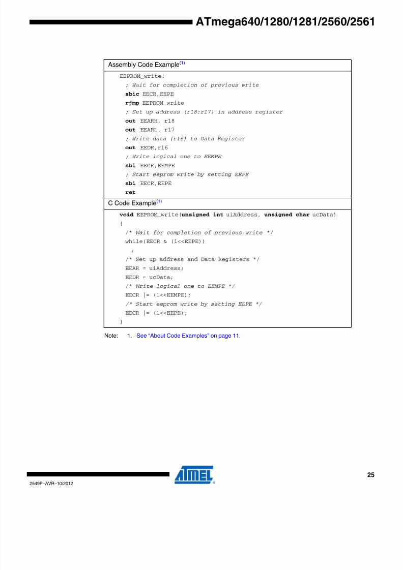
Note: 1. See “About Code Examples” on page 11.
Assembly Code Example(1)
EEPROM_write:
; Wait for completion of previous write
sbic EECR,EEPE
rjmp EEPROM_write
; Set up address (r18:r17) in address register
out EEARH, r18
out EEARL, r17
; Write data (r16) to Data Register
out EEDR,r16
; Write logical one to EEMPE
sbi EECR,EEMPE
; Start eeprom write by setting EEPE
sbi EECR,EEPE
ret
C Code Example(1)
void EEPROM_write( unsigned int uiAddress, unsigned char ucData)
{
/* Wait for completion of previous write */
while(EECR & (1<<EEPE))
;
/* Set up address and Data Registers */
EEAR = uiAddress;
EEDR = ucData;
/* Write logical one to EEMPE */
EECR |= (1<<EEMPE);
/* Start eeprom write by setting EEPE */
EECR |= (1<<EEPE);
}

8/20/2019 At Mega 1281 Unlocked
http://slidepdf.com/reader/full/at-mega-1281-unlocked 26/446
26
2549P–AVR–10/2012
ATmega640/1280/1281/2560/2561
The next code examples show assembly and C functions for reading the EEPROM. The exam
ples assume that interrupts are controlled so that no interrupts will occur during execution o
these functions.
Note: 1. See “About Code Examples” on page 11.
8.3.2 Preventing EEPROM Corruption
During periods of low VCC, the EEPROM data can be corrupted because the supply voltage is
too low for the CPU and the EEPROM to operate properly. These issues are the same as fo
board level systems using EEPROM, and the same design solutions should be applied.
An EEPROM data corruption can be caused by two situations when the voltage is too low. First
a regular write sequence to the EEPROM requires a minimum voltage to operate correctly. Sec
ondly, the CPU itself can execute instructions incorrectly, if the supply voltage is too low.
EEPROM data corruption can easily be avoided by following this design recommendation:
Keep the AVR RESET active (low) during periods of insufficient power supply voltage. This can
be done by enabling the internal Brown-out Detector (BOD). If the detection level of the interna
BOD does not match the needed detection level, an external low VCC reset Protection circuit can
be used. If a reset occurs while a write operation is in progress, the write operation will be com-
pleted provided that the power supply voltage is sufficient.
Assembly Code Example(1)
EEPROM_read:
; Wait for completion of previous write
sbic EECR,EEPE
rjcmp EEPROM_read
; Set up address (r18:r17) in address register
out EEARH, r18
out EEARL, r17
; Start eeprom read by writing EERE
sbi EECR,EERE
; Read data from Data Register
in r16,EEDR
ret
C Code Example(1)
unsigned char EEPROM_read( unsigned int uiAddress)
{
/* Wait for completion of previous write */
while(EECR & (1<<EEPE))
;
/* Set up address register */
EEAR = uiAddress;
/* Start eeprom read by writing EERE */
EECR |= (1<<EERE);
/* Return data from Data Register */
return EEDR;
}

8/20/2019 At Mega 1281 Unlocked
http://slidepdf.com/reader/full/at-mega-1281-unlocked 27/446
27
2549P–AVR–10/2012
ATmega640/1280/1281/2560/2561
8.4 I/O Memory
The I/O space definition of the ATmega640/1280/1281/2560/2561 is shown in “Register Sum
mary” on page 411.
All ATmega640/1280/1281/2560/2561 I/Os and peripherals are placed in the I/O space. All I/O
locations may be accessed by the LD/LDS/LDD and ST/STS/STD instructions, transferring data
between the 32 general purpose working registers and the I/O space. I/O Registers within theaddress range 0x00 - 0x1F are directly bit-accessible using the SBI and CBI instructions. In
these registers, the value of single bits can be checked by using the SBIS and SBIC instructions
Refer to the “Instruction Set Summary” on page 416 for more details. When using the I/O spe-
cific commands IN and OUT, the I/O addresses 0x00 - 0x3F must be used. When addressing I/O
Registers as data space using LD and ST instructions, 0x20 must be added to these addresses
The ATmega640/1280/1281/2560/2561 is a complex microcontroller with more peripheral units
than can be supported within the 64 location reserved in Opcode for the IN and OUT instruc
tions. For the Extended I/O space from 0x60 - 0x1FF in SRAM, only the ST/STS/STD and
LD/LDS/LDD instructions can be used.
For compatibility with future devices, reserved bits should be written to zero if accessed
Reserved I/O memory addresses should never be written.
Some of the Status Flags are cleared by writing a logical one to them. Note that, unlike mos
other AVRs, the CBI and SBI instructions will only operate on the specified bit, and can therefore
be used on registers containing such Status Flags. The CBI and SBI instructions work with reg-
isters 0x00 to 0x1F only.
The I/O and peripherals control registers are explained in later sections.
8.4.1 General Purpose I/O Registers
The ATmega640/1280/1281/2560/2561 contains three General Purpose I/O Registers. These
registers can be used for storing any information, and they are particularly useful for storing
global variables and Status Flags. General Purpose I/O Registers within the address range 0x00
- 0x1F are directly bit-accessible using the SBI, CBI, SBIS, and SBIC instructions. See “RegisteDescription” on page 35.

8/20/2019 At Mega 1281 Unlocked
http://slidepdf.com/reader/full/at-mega-1281-unlocked 28/446
28
2549P–AVR–10/2012
ATmega640/1280/1281/2560/2561
9. External Memory Interface
With all the features the External Memory Interface provides, it is well suited to operate as an
interface to memory devices such as External SRAM and Flash, and peripherals such as LCD-
display, A/D, and D/A. The main features are:
• Four different wait-state settings (including no wait-state)
• Independent wait-state setting for different External Memory sectors (configurable sector size)
• The number of bits dedicated to address high byte is selectable
• Bus keepers on data lines to minimize current consumption (optional)
9.1 Overview
When the eXternal MEMory (XMEM) is enabled, address space outside the internal SRAM
becomes available using the dedicated External Memory pins (see Figure 1-3 on page 4, Table
13-3 on page 78, Table 13-9 on page 82, and Table 13-21 on page 90). The memory configura
tion is shown in Figure 9-1.
Figure 9-1. External Memory with Sector Select
Memory Configuration A
0x0000
0x21FF
External Memory(0 - 60K x 8)
0xFFFF
Internal memory
SRL[2..0]
SRW11
SRW10
SRW01
SRW00
Lower sector
Upper sector
0x2200

8/20/2019 At Mega 1281 Unlocked
http://slidepdf.com/reader/full/at-mega-1281-unlocked 29/446
29
2549P–AVR–10/2012
ATmega640/1280/1281/2560/2561
9.1.1 Using the External Memory Interface
The interface consists of:
• AD7:0: Multiplexed low-order address bus and data bus
• A15:8: High-order address bus (configurable number of bits)
• ALE: Address latch enable
• RD: Read strobe• WR: Write strobe
The control bits for the External Memory Interface are located in two registers, the Externa
Memory Control Register A – XMCRA, and the External Memory Control Register B – XMCRB.
When the XMEM interface is enabled, the XMEM interface will override the setting in the data
direction registers that corresponds to the ports dedicated to the XMEM interface. For details
about the port override, see the alternate functions in section “I/O-Ports” on page 70. The XMEM
interface will auto-detect whether an access is internal or external. If the access is external, the
XMEM interface will output address, data, and the control signals on the ports according to Fig
ure 9-3 on page 31 (this figure shows the wave forms without wait-states). When ALE goes from
high-to-low, there is a valid address on AD7:0. ALE is low during a data transfer. When the
XMEM interface is enabled, also an internal access will cause activity on address, data and ALEports, but the RD and WR strobes will not toggle during internal access. When the Externa
Memory Interface is disabled, the normal pin and data direction settings are used. Note tha
when the XMEM interface is disabled, the address space above the internal SRAM boundary is
not mapped into the internal SRAM. Figure 9-2 on page 30 illustrates how to connect an externa
SRAM to the AVR using an octal latch (typically “74 × 573” or equivalent) which is transparent
when G is high.
9.1.2 Address Latch Requirements
Due to the high-speed operation of the XRAM interface, the address latch must be selected with
care for system frequencies above 8MHz @ 4V and 4MHz @ 2.7V. When operating at condi
tions above these frequencies, the typical old style 74HC series latch becomes inadequate. The
External Memory Interface is designed in compliance to the 74AHC series latch. However, mos
latches can be used as long they comply with the main timing parameters. The main parameters
for the address latch are:
• D to Q propagation delay (tPD)
• Data setup time before G low (tSU)
• Data (address) hold time after G low (TH)
The External Memory Interface is designed to guaranty minimum address hold time after G is
asserted low of th = 5ns. Refer to tLAXX_LD /tLLAXX_ST in “External Data Memory Timing” Tables 31
11 through Tables 31-18 on pages 379 - 382. The D-to-Q propagation delay (tPD) must be taken
into consideration when calculating the access time requirement of the external component. The
data setup time before G low (tSU
) must not exceed address valid to ALE low (tAVLLC
) minus PCB
wiring delay (dependent on the capacitive load).
8/20/2019 At Mega 1281 Unlocked
http://slidepdf.com/reader/full/at-mega-1281-unlocked 30/446
30
2549P–AVR–10/2012
ATmega640/1280/1281/2560/2561
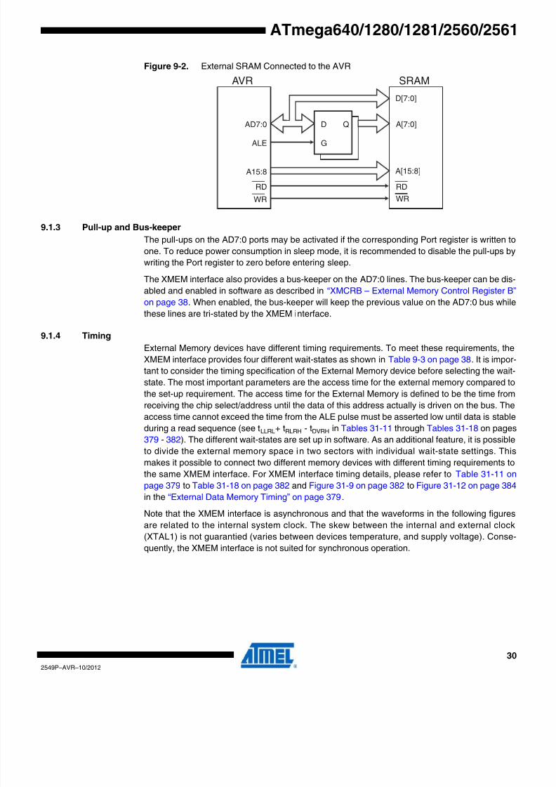
Figure 9-2. External SRAM Connected to the AVR
9.1.3 Pull-up and Bus-keeper
The pull-ups on the AD7:0 ports may be activated if the corresponding Port register is written to
one. To reduce power consumption in sleep mode, it is recommended to disable the pull-ups by
writing the Port register to zero before entering sleep.
The XMEM interface also provides a bus-keeper on the AD7:0 lines. The bus-keeper can be dis-
abled and enabled in software as described in “XMCRB – External Memory Control Register B”
on page 38. When enabled, the bus-keeper will keep the previous value on the AD7:0 bus while
these lines are tri-stated by the XMEM interface.
9.1.4 Timing
External Memory devices have different timing requirements. To meet these requirements, the
XMEM interface provides four different wait-states as shown in Table 9-3 on page 38. It is impor
tant to consider the timing specification of the External Memory device before selecting the wait-
state. The most important parameters are the access time for the external memory compared to
the set-up requirement. The access time for the External Memory is defined to be the time from
receiving the chip select/address until the data of this address actually is driven on the bus. Theaccess time cannot exceed the time from the ALE pulse must be asserted low until data is stable
during a read sequence (see tLLRL+ tRLRH - tDVRH in Tables 31-11 through Tables 31-18 on pages
379 - 382). The different wait-states are set up in software. As an additional feature, it is possible
to divide the external memory space in two sectors with individual wait-state settings. This
makes it possible to connect two different memory devices with different timing requirements to
the same XMEM interface. For XMEM interface timing details, please refer to Table 31-11 on
page 379 to Table 31-18 on page 382 and Figure 31-9 on page 382 to Figure 31-12 on page 384
in the “External Data Memory Timing” on page 379.
Note that the XMEM interface is asynchronous and that the waveforms in the following figures
are related to the internal system clock. The skew between the internal and external clock
(XTAL1) is not guarantied (varies between devices temperature, and supply voltage). Consequently, the XMEM interface is not suited for synchronous operation.
D[7:0]
A[7:0]
A[15:8]
RD
WR
SRAM
D Q
G
AD7:0
ALE
A15:8
RD
WR
AVR

8/20/2019 At Mega 1281 Unlocked
http://slidepdf.com/reader/full/at-mega-1281-unlocked 31/446
31
2549P–AVR–10/2012
ATmega640/1280/1281/2560/2561
Figure 9-3. External Data Memory Cycles without Wait-state (SRWn1=0 and SRWn0=0)(1)
Note: 1. SRWn1 = SRW11 (upper sector) or SRW01 (lower sector), SRWn0 = SRW10 (upper sector) orSRW00 (lower sector). The ALE pulse in period T4 is only present if the next instructionaccesses the RAM (internal or external).
Figure 9-4. External Data Memory Cycles with SRWn1 = 0 and SRWn0 = 1(1)
Note: 1. SRWn1 = SRW11 (upper sector) or SRW01 (lower sector), SRWn0 = SRW10 (upper sector) orSRW00 (lower sector).The ALE pulse in period T5 is only present if the next instruction accesses the RAM (internal
or external).
ALE
T1 T2 T3
Write
Read
WR
T4
A15:8 AddressPrev. addr.
DA7:0 Address DataPrev. data XX
RD
DA7:0 (XMBK = 0) DataPrev. data Address
DataPrev. data AddressDA7:0 (XMBK = 1)
System Clock (CLKCPU)
XXXXX XXXXXXXX
ALE
T1 T2 T3
W r i t e
R e a
d
WR
T5
A15:8 AddressPrev. addr.
DA7:0 Address DataPrev. data XX
RD
DA7:0 (XMBK = 0) DataPrev. data Address
DataPrev. data AddressDA7:0 (XMBK = 1)
System Clock (CLKCPU)
T4

8/20/2019 At Mega 1281 Unlocked
http://slidepdf.com/reader/full/at-mega-1281-unlocked 32/446
32
2549P–AVR–10/2012
ATmega640/1280/1281/2560/2561
Figure 9-5. External Data Memory Cycles with SRWn1 = 1 and SRWn0 = 0(1)
Note: 1. SRWn1 = SRW11 (upper sector) or SRW01 (lower sector), SRWn0 = SRW10 (upper sector) oSRW00 (lower sector).The ALE pulse in period T6 is only present if the next instruction accesses the RAM (interna
or external).
Figure 9-6. External Data Memory Cycles with SRWn1 = 1 and SRWn0 = 1(1)
Note: 1. SRWn1 = SRW11 (upper sector) or SRW01 (lower sector), SRWn0 = SRW10 (upper sector) orSRW00 (lower sector).The ALE pulse in period T7 is only present if the next instruction accesses the RAM (internalor external).
9.1.5 Using all Locations of External Memory Smaller than 64Kbytes
Since the external memory is mapped after the internal memory as shown in Figure 9-1 on page
28, the external memory is not addressed when addressing the first 8,704 bytes of data space. I
may appear that the first 8,704 bytes of the external memory are inaccessible (external memory
addresses 0x0000 to 0x21FF). However, when connecting an external memory smaller than
64Kbytes, for example 32Kbytes, these locations are easily accessed simply by addressing from
address 0x8000 to 0xA1FF. Since the External Memory Address bit A15 is not connected to the
external memory, addresses 0x8000 to 0xA1FF will appear as addresses 0x0000 to 0x21FF fo
the external memory. Addressing above address 0xA1FF is not recommended, since this wil
address an external memory location that is already accessed by another (lower) address. To
the Application software, the external 32Kbytes memory will appear as one linear 32Kbytes
ALE
T1 T2 T3
W r i t e
R e a d
WR
T6
A15:8 AddressPrev. addr.
DA7:0 Address DataPrev. data XX
RD
DA7:0 (XMBK = 0) DataPrev. data Address
DataPrev. data AddressDA7:0 (XMBK = 1)
System Clock (CLKCPU)
T4 T5
ALE
T1 T2 T3
W r i t e
R e
a d
WR
T7
A15:8 AddressPrev. addr.
DA7:0 Address DataPrev. data XX
RD
DA7:0 (XMBK = 0) DataPrev. data Address
DataPrev. data AddressDA7:0 (XMBK = 1)
System Clock (CLKCPU)
T4 T5 T6

8/20/2019 At Mega 1281 Unlocked
http://slidepdf.com/reader/full/at-mega-1281-unlocked 33/446
33
2549P–AVR–10/2012
ATmega640/1280/1281/2560/2561
address space from 0x2200 to 0xA1FF. This is illustrated in Figure 9-7.
Figure 9-7. Address Map with 32Kbytes External Memory
9.1.6 Using all 64Kbytes Locations of External Memory
Since the External Memory is mapped after the Internal Memory as shown in Figure 9-1 on page
28, only 56Kbytes of External Memory is available by default (address space 0x0000 to 0x21FF
is reserved for internal memory). However, it is possible to take advantage of the entire Externa
Memory by masking the higher address bits to zero. This can be done by using the XMMn bits
and control by software the most significant bits of the address. By setting Port C to output 0x00
and releasing the most significant bits for normal Port Pin operation, the Memory Interface wil
address 0x0000 - 0x2FFF. See the following code examples.
Care must be exercised using this option as most of the memory is masked away.
0x0000
0x21FF
0x2200
0x7FFF
0x8000
0x90FF
0x9100
0x0000
0x7FFF
Internal Memory
AVR Memory Map External 32K SRAM
External
Memory

8/20/2019 At Mega 1281 Unlocked
http://slidepdf.com/reader/full/at-mega-1281-unlocked 34/446
34
2549P–AVR–10/2012
ATmega640/1280/1281/2560/2561
Note: 1. See “About Code Examples” on page 11.
Assembly Code Example(1)
; OFFSET is defined to 0x4000 to ensure; external memory access; Configure Port C (address high byte) to; output 0x00 when the pins are released; for normal Port Pin operation
ldi r16, 0xFFout DDRC, r16ldi r16, 0x00out PORTC, r16; release PC7:6ldi r16, (1<<XMM1)sts XMCRB, r16; write 0xAA to address 0x0001 of external; memoryldi r16, 0xaasts 0x0001+OFFSET, r16; re-enable PC7:6 for external memoryldi r16, (0<<XMM1)sts XMCRB, r16; store 0x55 to address (OFFSET + 1) of; external memoryldi r16, 0x55sts 0x0001+OFFSET, r16
C Code Example(1)
#define OFFSET 0x4000
void XRAM_example( void)
{
unsigned char *p = (unsigned char *) (OFFSET + 1);
DDRC = 0xFF;
PORTC = 0x00;
XMCRB = (1<<XMM1);
*p = 0xaa;
XMCRB = 0x00;
*p = 0x55;
}

8/20/2019 At Mega 1281 Unlocked
http://slidepdf.com/reader/full/at-mega-1281-unlocked 35/446
35
2549P–AVR–10/2012
ATmega640/1280/1281/2560/2561
9.2 Register Description
9.2.1 EEPROM registers
9.2.1.1 EEARH and EEARL – The EEPROM Address Register
• Bits 15:12 – Res: Reserved Bits
These bits are reserved bits and will always read as zero.
• Bits 11:0 – EEAR8:0: EEPROM Address
The EEPROM Address Registers – EEARH and EEARL specify the EEPROM address in the4Kbytes EEPROM space. The EEPROM data bytes are addressed linearly between 0 and
4096. The initial value of EEAR is undefined. A proper value must be written before the
EEPROM may be accessed.
9.2.1.2 EEDR – The EEPROM Data Register
• Bits 7:0 – EEDR7:0: EEPROM Data
For the EEPROM write operation, the EEDR Register contains the data to be written to theEEPROM in the address given by the EEAR Register. For the EEPROM read operation, the
EEDR contains the data read out from the EEPROM at the address given by EEAR.
9.2.1.3 EECR – The EEPROM Control Register
• Bits 7:6 – Res: Reserved Bits
These bits are reserved bits and will always read as zero.
• Bits 5, 4 – EEPM1 and EEPM0: EEPROM Programming Mode Bits
The EEPROM Programming mode bit setting defines which programming action that will be trig-
gered when writing EEPE. It is possible to program data in one atomic operation (erase the old
value and program the new value) or to split the Erase and Write operations in two differen
operations. The Programming times for the different modes are shown in Table 9-1 on page 36
While EEPE is set, any write to EEPMn will be ignored. During reset, the EEPMn bits will be
reset to 0b00 unless the EEPROM is busy programming.
Bit 15 14 13 12 11 10 9 8
0x22 (0x42) – – – – EEAR11 EEAR10 EEAR9 EEAR8 EEARH
0x21 (0x41) EEAR7 EEAR6 EEAR5 EEAR4 EEAR3 EEAR2 EEAR1 EEAR0 EEARL
7 6 5 4 3 2 1 0
Read/ Write R R R R R/ W R/ W R/ W R/ W
R/ W R/ W R/ W R/ W R/ W R/ W R/ W R/ W
Initial Value 0 0 0 0 X X X X
X X X X X X X X
Bit 7 6 5 4 3 2 1 0
0x20 (0x40) MSB LSB EEDR
Read/ Write R/ W R/ W R/ W R/ W R/ W R/ W R/ W R/ W
Initial Value 0 0 0 0 0 0 0 0
Bit 7 6 5 4 3 2 1 0
0x1F (0x3F) – – EEPM1 EEPM0 EERIE EEMPE EEPE EERE EECR
Read/ Write R R R/ W R/ W R/ W R/ W R/ W R/ W
Initial Value 0 0 X X 0 0 X 0

8/20/2019 At Mega 1281 Unlocked
http://slidepdf.com/reader/full/at-mega-1281-unlocked 36/446
36
2549P–AVR–10/2012
ATmega640/1280/1281/2560/2561
• Bit 3 – EERIE: EEPROM Ready Interrupt Enable
Writing EERIE to one enables the EEPROM Ready Interrupt if the I bit in SREG is set. Writing
EERIE to zero disables the interrupt. The EEPROM Ready interrupt generates a constant inter
rupt when EEPE is cleared.
• Bit 2 – EEMPE: EEPROM Master Programming Enable
The EEMPE bit determines whether setting EEPE to one causes the EEPROM to be written
When EEMPE is set, setting EEPE within four clock cycles will write data to the EEPROM at theselected address If EEMPE is zero, setting EEPE will have no effect. When EEMPE has been
written to one by software, hardware clears the bit to zero after four clock cycles. See the
description of the EEPE bit for an EEPROM write procedure.
• Bit 1 – EEPE: EEPROM Programming Enable
The EEPROM Write Enable Signal EEPE is the write strobe to the EEPROM. When address
and data are correctly set up, the EEPE bit must be written to one to write the value into the
EEPROM. The EEMPE bit must be written to one before a logical one is written to EEPE, other
wise no EEPROM write takes place. The following procedure should be followed when writing
the EEPROM (the order of steps 3 and 4 is not essential):
1. Wait until EEPE becomes zero.2. Wait until SPMEN in SPMCSR becomes zero.
3. Write new EEPROM address to EEAR (optional).
4. Write new EEPROM data to EEDR (optional).
5. Write a logical one to the EEMPE bit while writing a zero to EEPE in EECR.
6. Within four clock cycles after setting EEMPE, write a logical one to EEPE.
The EEPROM can not be programmed during a CPU write to the Flash memory. The software
must check that the Flash programming is completed before initiating a new EEPROM write
Step 2 is only relevant if the software contains a Boot Loader allowing the CPU to program the
Flash. If the Flash is never being updated by the CPU, step 2 can be omitted. See “Memory Pro
gramming” on page 335 for details about Boot programming.
Caution: An interrupt between step 5 and step 6 will make the write cycle fail, since the
EEPROM Master Write Enable will time-out. If an interrupt routine accessing the EEPROM is
interrupting another EEPROM access, the EEAR or EEDR Register will be modified, causing the
interrupted EEPROM access to fail. It is recommended to have the Global Interrupt Flag cleared
during all the steps to avoid these problems.
When the write access time has elapsed, the EEPE bit is cleared by hardware. The user soft-
ware can poll this bit and wait for a zero before writing the next byte. When EEPE has been set
the CPU is halted for two cycles before the next instruction is executed.
Table 9-1. EEPROM Mode Bits
EEPM1 EEPM0
Programming
Time Operation
0 0 3.4ms Erase and Write in one operation (Atomic Operation)
0 1 1.8ms Erase only
1 0 1.8ms Write only
1 1 – Reserved for future use
8/20/2019 At Mega 1281 Unlocked
http://slidepdf.com/reader/full/at-mega-1281-unlocked 37/446
37
2549P–AVR–10/2012
ATmega640/1280/1281/2560/2561
• Bit 0 – EERE: EEPROM Read Enable
The EEPROM Read Enable Signal EERE is the read strobe to the EEPROM. When the correc
address is set up in the EEAR Register, the EERE bit must be written to a logic one to trigger the
EEPROM read. The EEPROM read access takes one instruction, and the requested data is
available immediately. When the EEPROM is read, the CPU is halted for four cycles before the
next instruction is executed.
The user should poll the EEPE bit before starting the read operation. If a write operation is in
progress, it is neither possible to read the EEPROM, nor to change the EEAR Register.
9.3 General Purpose registers
9.3.1 GPIOR2 – General Purpose I/O Register 2
9.3.2 GPIOR1 – General Purpose I/O Register 1
9.3.3 GPIOR0 – General Purpose I/O Register 0
9.4 External Memory registers
9.4.1 XMCRA – External Memory Control Register A
• Bit 7 – SRE: External SRAM/XMEM Enable
Writing SRE to one enables the External Memory Interface.The pin functions AD7:0, A15:8
ALE, WR, and RD are activated as the alternate pin functions. The SRE bit overrides any pindirection settings in the respective data direction registers. Writing SRE to zero, disables the
External Memory Interface and the normal pin and data direction settings are used.
• Bit 6:4 – SRL2:0: Wait-state Sector Limit
It is possible to configure different wait-states for different External Memory addresses. The
external memory address space can be divided in two sectors that have separate wait-state bits
The SRL2, SRL1, and SRL0 bits select the split of the sectors, see Table 9-2 on page 38 and
Bit 7 6 5 4 3 2 1 0
0x2B (0x4B) MSB LSB GPIOR2
Read/ Write R/ W R/ W R/ W R/ W R/ W R/ W R/ W R/ W
Initial Value 0 0 0 0 0 0 0 0
Bit 7 6 5 4 3 2 1 0
0x2A (0x4A) MSB LSB GPIOR1
Read/ Write R/ W R/ W R/ W R/ W R/ W R/ W R/ W R/ W
Initial Value 0 0 0 0 0 0 0 0
Bit 7 6 5 4 3 2 1 0
0x1E (0x3E) MSB LSB GPIOR0
Read/ Write R/ W R/ W R/ W R/ W R/ W R/ W R/ W R/ W
Initial Value 0 0 0 0 0 0 0 0
Bit 7 6 5 4 3 2 1 0
“(0x74)” SRE SRL2 SRL1 SRL0 SRW11 SRW10 SRW01 SRW00 XMCRA
Read/ Write R/ W R/ W R/ W R/ W R/ W R/ W R/ W R/ W
Initial Value 0 0 0 0 0 0 0 0
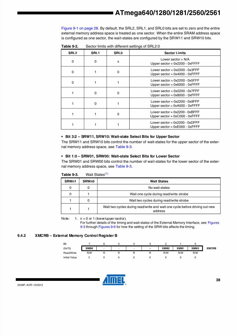
8/20/2019 At Mega 1281 Unlocked
http://slidepdf.com/reader/full/at-mega-1281-unlocked 38/446
38
2549P–AVR–10/2012
ATmega640/1280/1281/2560/2561
Figure 9-1 on page 28. By default, the SRL2, SRL1, and SRL0 bits are set to zero and the entire
external memory address space is treated as one sector. When the entire SRAM address space
is configured as one sector, the wait-states are configured by the SRW11 and SRW10 bits.
• Bit 3:2 – SRW11, SRW10: Wait-state Select Bits for Upper Sector
The SRW11 and SRW10 bits control the number of wait-states for the upper sector of the exter-
nal memory address space, see Table 9-3.
• Bit 1:0 – SRW01, SRW00: Wait-state Select Bits for Lower Sector
The SRW01 and SRW00 bits control the number of wait-states for the lower sector of the exter
nal memory address space, see Table 9-3.
Note: 1. n = 0 or 1 (lower/upper sector).For further details of the timing and wait-states of the External Memory Interface, see Figures9-3 through Figures 9-6 for how the setting of the SRW bits affects the timing.
9.4.2 XMCRB – External Memory Control Register B
Table 9-2. Sector limits with different settings of SRL2:0
SRL2 SRL1 SRL0 Sector Limits
0 0 xLower sector = N /A
Upper sector = 0x2200 - 0xFFFF
0 1 0Lower sector = 0x2200 - 0x3FFFUpper sector = 0x4000 - 0xFFFF
0 1 1Lower sector = 0x2200 - 0x5FFFUpper sector = 0x6000 - 0xFFFF
1 0 0Lower sector = 0x2200 - 0x7FFFUpper sector = 0x8000 - 0xFFFF
1 0 1Lower sector = 0x2200 - 0x9FFFUpper sector = 0xA000 - 0xFFFF
1 1 0
Lower sector = 0x2200 - 0xBFFF
Upper sector = 0xC000 - 0xFFFF
1 1 1Lower sector = 0x2200 - 0xDFFFUpper sector = 0xE000 - 0xFFFF
Table 9-3. Wait States(1)
SRWn1 SRWn0 Wait States
0 0 No wait-states
0 1 Wait one cycle during read/write strobe
1 0 Wait two cycles during read/write strobe
1 1 Wait two cycles during read/write and wait one cycle before driving out new
address
Bit 7 6 5 4 3 2 1 0
(0x75) XMBK – – – – XMM2 XMM1 XMM0 XMCRB
Read/ Write R/ W R R R R R/ W R/ W R/ W
Initial Value 0 0 0 0 0 0 0 0
8/20/2019 At Mega 1281 Unlocked
http://slidepdf.com/reader/full/at-mega-1281-unlocked 39/446
39
2549P–AVR–10/2012
ATmega640/1280/1281/2560/2561
• Bit 7– XMBK: External Memory Bus-keeper Enable
Writing XMBK to one enables the bus keeper on the AD7:0 lines. When the bus keeper is
enabled, AD7:0 will keep the last driven value on the lines even if the XMEM interface has tri
stated the lines. Writing XMBK to zero disables the bus keeper. XMBK is not qualified with SRE
so even if the XMEM interface is disabled, the bus keepers are still activated as long as XMBK isone.
• Bit 6:3 – Res: Reserved Bits
These bits are reserved and will always read as zero. When writing to this address location
write these bits to zero for compatibility with future devices.
• Bit 2:0 – XMM2, XMM1, XMM0: External Memory High Mask
When the External Memory is enabled, all Port C pins are default used for the high address byte
If the full 60Kbytes address space is not required to access the External Memory, some, or all,
Port C pins can be released for normal Port Pin function as described in Table 9-4. As described
in “Using all 64Kbytes Locations of External Memory” on page 33, it is possible to use the XMMn
bits to access all 64Kbytes locations of the External Memory.
Table 9-4. Port C Pins Released as Normal Port Pins when the External Memory is Enabled
XMM2 XMM1 XMM0 # Bits for External Memory Address Released Port Pins
0 0 0 8 (Full 56Kbytes space) None
0 0 1 7 PC7
0 1 0 6 PC7 - PC6
0 1 1 5 PC7 - PC5
1 0 0 4 PC7 - PC4
1 0 1 3 PC7 - PC3
1 1 0 2 PC7 - PC2
1 1 1 No Address high bits Full Port C

8/20/2019 At Mega 1281 Unlocked
http://slidepdf.com/reader/full/at-mega-1281-unlocked 40/446
40
2549P–AVR–10/2012
ATmega640/1280/1281/2560/2561
10. System Clock and Clock OptionsThis section describes the clock options for the AVR microcontroller.
10.1 Overview
Figure 10-1 presents the principal clock systems in the AVR and their distribution. All of the
clocks need not be active at a given time. In order to reduce power consumption, the clocks tomodules not being used can be halted by using different sleep modes, as described in “Powe
Management and Sleep Modes” on page 52. The clock systems are detailed below.
Figure 10-1. Clock Distribution.
10.2 Clock Systems and their Distribution
10.2.1 CPU Clock – clk CPU
The CPU clock is routed to parts of the system concerned with operation of the AVR core
Examples of such modules are the General Purpose Register File, the Status Register and the
data memory holding the Stack Pointer. Halting the CPU clock inhibits the core from performing
general operations and calculations.
General I/O
Modules
Asynchronous
Timer/CounterCPU Core RAM
clkI/O
clkASY
AVR ClockControl Unit
clkCPU
Flash and
EEPROM
clkFLASH
Source clock
Watchdog Timer
Watchdog
Oscillator
Reset Logic
ClockMultiplexer
Watchdog clock
Calibrated RC
Oscillator
Timer/Counter
Oscillator
Crystal
Oscillator
Low-frequency
Crystal OscillatorExternal Clock
ADC
clkADC
System ClockPrescaler
8/20/2019 At Mega 1281 Unlocked
http://slidepdf.com/reader/full/at-mega-1281-unlocked 41/446
41
2549P–AVR–10/2012
ATmega640/1280/1281/2560/2561
10.2.2 I/O Clock – clk I/OThe I/O clock is used by the majority of the I/O modules, like Timer/Counters, SPI, and USART
The I/O clock is also used by the External Interrupt module, but note that some external inter-
rupts are detected by asynchronous logic, allowing such interrupts to be detected even if the I/O
clock is halted. Also note that start condition detection in the USI module is carried out asynchro-
nously when clkI/O is halted, TWI address recognition in all sleep modes.
10.2.3 Flash Clock – clk FLASH
The Flash clock controls operation of the Flash interface. The Flash clock is usually active simul-
taneously with the CPU clock.
10.2.4 Asynchronous Timer Clock – clk ASY
The Asynchronous Timer clock allows the Asynchronous Timer/Counter to be clocked directly
from an external clock or an external 32kHz clock crystal. The dedicated clock domain allows
using this Timer/Counter as a real-time counter even when the device is in sleep mode.
10.2.5 ADC Clock – clk ADC
The ADC is provided with a dedicated clock domain. This allows halting the CPU and I/O clocks
in order to reduce noise generated by digital circuitry. This gives more accurate ADC conversion
results.
10.3 Clock Sources
The device has the following clock source options, selectable by Flash Fuse bits as shown
below. The clock from the selected source is input to the AVR clock generator, and routed to the
appropriate modules.
Note: 1. For all fuses “1” means unprogrammed while “0” means programmed.
Table 10-1. Device Clocking Options Select(1)
Device Clocking Option CKSEL3:0
Low Power Crystal Oscillator 1111 - 1000
Full Swing Crystal Oscillator 0111 - 0110
Low Frequency Crystal Oscillator 0101 - 0100
Internal 128kHz RC Oscillator 0011
Calibrated Internal RC Oscillator 0010
External Clock 0000
Reserved 0001

8/20/2019 At Mega 1281 Unlocked
http://slidepdf.com/reader/full/at-mega-1281-unlocked 42/446
42
2549P–AVR–10/2012
ATmega640/1280/1281/2560/2561
10.3.1 Default Clock Source
The device is shipped with internal RC oscillator at 8.0MHz and with the fuse CKDIV8 pro
grammed, resulting in 1.0MHz system clock. The startup time is set to maximum and time-out
period enabled. (CKSEL = "0010", SUT = "10", CKDIV8 = "0"). The default setting ensures that
all users can make their desired clock source setting using any available programming interface
10.3.2 Clock Start-up Sequence
Any clock source needs a sufficient VCC to start oscillating and a minimum number of oscillating
cycles before it can be considered stable.
To ensure sufficient VCC, the device issues an internal reset with a time-out delay (tTOUT) afte
the device reset is released by all other reset sources. “On-chip Debug System” on page 55
describes the start conditions for the internal reset. The delay (tTOUT) is timed from the Watchdog
Oscillator and the number of cycles in the delay is set by the SUTx and CKSELx fuse bits. The
selectable delays are shown in Table 10-2. The frequency of the Watchdog Oscillator is voltage
dependent as shown in “Typical Characteristics” on page 385.
Main purpose of the delay is to keep the AVR in reset until it is supplied with minimum VCC. The
delay will not monitor the actual voltage and it will be required to select a delay longer than the
Vcc rise time. If this is not possible, an internal or external Brown-Out Detection circuit should be
used. A BOD circuit will ensure sufficient VCC before it releases the reset, and the time-out delay
can be disabled. Disabling the time-out delay without utilizing a Brown-Out Detection circuit is
not recommended.
The oscillator is required to oscillate for a minimum number of cycles before the clock is consid-
ered stable. An internal ripple counter monitors the oscillator output clock, and keeps the interna
reset active for a given number of clock cycles. The reset is then released and the device wil
start to execute. The recommended oscillator start-up time is dependent on the clock type, and
varies from 6 cycles for an externally applied clock to 32K cycles for a low frequency crystal.
The start-up sequence for the clock includes both the time-out delay and the start-up time when
the device starts up from reset. When starting up from Power-save or Power-down mode, VCC is
assumed to be at a sufficient level and only the start-up time is included.
10.4 Low Power Crystal OscillatorPins XTAL1 and XTAL2 are input and output, respectively, of an inverting amplifier which can be
configured for use as an On-chip Oscillator, as shown in Figure 10-2. Either a quartz crystal or a
ceramic resonator may be used.
This Crystal Oscillator is a low power oscillator, with reduced voltage swing on the XTAL2 out
put. It gives the lowest power consumption, but is not capable of driving other clock inputs, and
may be more susceptible to noise in noisy environments. In these cases, refer to the “Full Swing
Crystal Oscillator” on page 44.
Table 10-2. Number of Watchdog Oscillator Cycles
Typ Time-out (VCC = 5.0V) Typ Time-out (VCC = 3.0V) Number of Cycles
0ms 0ms 0
4.1ms 4.3ms 512
65ms 69ms 8K (8,192)

8/20/2019 At Mega 1281 Unlocked
http://slidepdf.com/reader/full/at-mega-1281-unlocked 43/446
43
2549P–AVR–10/2012
ATmega640/1280/1281/2560/2561
C1 and C2 should always be equal for both crystals and resonators. The optimal value of the
capacitors depends on the crystal or resonator in use, the amount of stray capacitance, and the
electromagnetic noise of the environment. Some initial guidelines for choosing capacitors for
use with crystals are given in Table 10-3. For ceramic resonators, the capacitor values given by
the manufacturer should be used.
Figure 10-2. Crystal Oscillator Connections
The Low Power Oscillator can operate in three different modes, each optimized for a specific frequency range. The operating mode is selected by the fuses CKSEL3:1 as shown in Table 10-3.
Notes: 1. This is the recommended CKSEL settings for the different frequency ranges.
2. This option should not be used with crystals, only with ceramic resonators.3. If 8MHz frequency exceeds the specification of the device (depends on VCC), the CKDIV8
Fuse can be programmed in order to divide the internal frequency by 8. It must be ensuredthat the resulting divided clock meets the frequency specification of the device.
4. Maximum frequency when using ceramic oscillator is 10MHz.
The CKSEL0 Fuse together with the SUT1:0 Fuses select the start-up times as shown in Table
10-4.
Table 10-3. Low Power Crystal Oscillator Operating Modes(3)
Frequency Range (MHz) CKSEL3:1(1) Recommended Range for Capacitors C1 and C2 (pF)
0.4 - 0.9 100(2) –
0.9 - 3.0 101 12 - 22
3.0 - 8.0 110 12 - 22
8.0 - 16.0(4) 111 12 - 22
Table 10-4. Start-up Times for the Low Power Crystal Oscillator Clock Selection
Oscillator Source /
Power Conditions
Start-up Time from
Power-down and
Power-save
Additional Delay
from Reset
(VCC = 5.0V) CKSEL0 SUT1:0
Ceramic resonator, fastrising power
258 CK 14CK + 4.1ms(1) 0 00
Ceramic resonator, slowlyrising power
258 CK 14CK + 65ms(1) 0 01
Ceramic resonator, BODenabled
1K CK 14CK(2) 0 10
XTAL2
XTAL1
GND
C2
C1

8/20/2019 At Mega 1281 Unlocked
http://slidepdf.com/reader/full/at-mega-1281-unlocked 44/446
44
2549P–AVR–10/2012
ATmega640/1280/1281/2560/2561
Notes: 1. These options should only be used when not operating close to the maximum frequency of thedevice, and only if frequency stability at start-up is not important for the application. Theseoptions are not suitable for crystals.
2. These options are intended for use with ceramic resonators and will ensure frequency stabilityat start-up. They can also be used with crystals when not operating close to the maximum frequency of the device, and if frequency stability at start-up is not important for the application.
10.5 Full Swing Crystal Oscillator
Pins XTAL1 and XTAL2 are input and output, respectively, of an inverting amplifier which can be
configured for use as an On-chip Oscillator, as shown in Figure 10-2 on page 43. Either a quartz
crystal or a ceramic resonator may be used.
This Crystal Oscillator is a full swing oscillator, with rail-to-rail swing on the XTAL2 output. This is
useful for driving other clock inputs and in noisy environments. The current consumption is
higher than the “Low Power Crystal Oscillator” on page 42. Note that the Full Swing Crysta
Oscillator will only operate for VCC = 2.7 - 5.5 volts.C1 and C2 should always be equal for both crystals and resonators. The optimal value of the
capacitors depends on the crystal or resonator in use, the amount of stray capacitance, and the
electromagnetic noise of the environment. Some initial guidelines for choosing capacitors for
use with crystals are given in Table 10-6 on page 45. For ceramic resonators, the capacitor val
ues given by the manufacturer should be used.
The operating mode is selected by the fuses CKSEL3:1 as shown in Table 10-5.
Note: 1. If 8MHz frequency exceeds the specification of the device (depends on VCC), the CKDIV8Fuse can be programmed in order to divide the internal frequency by 8. It must be ensuredthat the resulting divided clock meets the frequency specification of the device.
Ceramic resonator, fastrising power
1K CK 14CK + 4.1ms(2) 0 11
Ceramic resonator, slowlyrising power
1K CK 14CK + 65ms(2) 1 00
Crystal Oscillator, BODenabled
16K CK 14CK1
01
Crystal Oscillator, fastrising power
16K CK 14CK + 4.1ms1
10
Crystal Oscillator, slowlyrising power
16K CK 14CK + 65ms1
11
Table 10-4. Start-up Times for the Low Power Crystal Oscillator Clock Selection (Continued)
Oscillator Source /
Power Conditions
Start-up Time from
Power-down and
Power-save
Additional Delay
from Reset
(VCC = 5.0V) CKSEL0 SUT1:0
Table 10-5. Full Swing Crystal Oscillator operating modes(1)
Frequency Range (MHz) CKSEL3:1 Recommended Range for Capacitors C1 and C2 (pF)
0.4 - 16 011 12 - 22

8/20/2019 At Mega 1281 Unlocked
http://slidepdf.com/reader/full/at-mega-1281-unlocked 45/446
45
2549P–AVR–10/2012
ATmega640/1280/1281/2560/2561
Notes: 1. These options should only be used when not operating close to the maximum frequency of thedevice, and only if frequency stability at start-up is not important for the application. Theseoptions are not suitable for crystals.
2. These options are intended for use with ceramic resonators and will ensure frequency stabilityat start-up. They can also be used with crystals when not operating close to the maximum frequency of the device, and if frequency stability at start-up is not important for the application.
10.6 Low Frequency Crystal OscillatorThe device can utilize a 32.768kHz watch crystal as clock source by a dedicated Low Frequency
Crystal Oscillator. The crystal should be connected as shown in Figure 10-3 on page 46. When
this Oscillator is selected, start-up times are determined by the SUT Fuses and CKSEL0 as
shown in Table 10-8 on page 46.
The Low-Frequency Crystal Oscillator provides an internal load capacitance, see Table 10-7 a
each XTAL/TOSC pin.
Table 10-6. Start-up Times for the Full Swing Crystal Oscillator Clock Selection
Oscillator Source /
Power Conditions
Start-up Time from
Power-down and
Power-save
Additional Delay
from Reset
(VCC = 5.0V) CKSEL0 SUT1:0
Ceramic resonator,fast rising power 258 CK 14CK + 4.1ms(1) 0 00
Ceramic resonator,slowly rising power
258 CK 14CK + 65ms(1) 0 01
Ceramic resonator,BOD enabled
1K CK 14CK(2) 0 10
Ceramic resonator,fast rising power
1K CK 14CK + 4.1ms(2) 0 11
Ceramic resonator,slowly rising power
1K CK 14CK + 65ms(2) 1 00
Crystal Oscillator,BOD enabled
16K CK 14CK 1 01
Crystal Oscillator,fast rising power
16K CK 14CK + 4.1ms 1 10
Crystal Oscillator,slowly rising power
16K CK 14CK + 65ms 1 11
Table 10-7. Capacitance for Low frequency oscillator
Device 32kHz oscillator Cap (Xtal1/Tosc1) Cap (Xtal2/Tosc2)
ATmega640/1280/1281/2560/2561 System Osc. 18pF 8pF
Timer Osc. 6pF 6pF

8/20/2019 At Mega 1281 Unlocked
http://slidepdf.com/reader/full/at-mega-1281-unlocked 46/446
46
2549P–AVR–10/2012
ATmega640/1280/1281/2560/2561
The capacitance (Ce + Ci) needed at each XTAL/TOSC pin can be calculated by using:
where:
Ce - is optional external capacitors as described in Figure 10-3 on page 46.Ci - is the pin capacitance in Table 10-7 on page 45.CL - is the load capacitance for a 32.768kHz crystal specified by the crystal vendor.CS - is the total stray capacitance for one XTAL/TOSC pin.
Crystals specifying load capacitance (CL) higher than the ones given in the Table 10-7 on page
45, require external capacitors applied as described in Figure 10-3 on page 46.
Figure 10-3. Crystal Oscillator Connections
To find suitable load capacitance for a 32.768kHz crysal, please consult the crystal datasheet.
When this oscillator is selected, start-up times are determined by the SUT Fuses and CKSEL0
as shown in Table 10-8.
Note: 1. These options should only be used if frequency stability at start-up is not important for theapplication.
Table 10-8. Start-up times for the low frequency crystal oscillator clock selection
Power Conditions
Start-up Time from
Power-down and
Power-save
Additional Delay
from Reset
(VCC = 5.0V) CKSEL0 SUT1:0
BOD enabled 1K CK 14CK(1) 0 00
Fast rising power 1K CK 14CK + 4.1ms(1) 0 01
Slowly rising power 1K CK 14CK + 65ms(1) 0 10
Reserved 0 11
BOD enabled 32K CK 14CK 1 00
Fast rising power 32K CK 14CK + 4.1ms 1 01
Slowly rising power 32K CK 14CK + 65ms 1 10
Reserved 1 11
Ce Ci+ 2 CL⋅ C s–=
Ce
CiCe
Ci
Cs
Cs
TOSC2
TOSC1
X1

8/20/2019 At Mega 1281 Unlocked
http://slidepdf.com/reader/full/at-mega-1281-unlocked 47/446
47
2549P–AVR–10/2012
ATmega640/1280/1281/2560/2561
10.7 Calibrated Internal RC Oscillator
By default, the Internal RC Oscillator provides an approximate 8MHz clock. Though voltage and
temperature dependent, this clock can be very accurately calibrated by the user. See Table 31-1
on page 371 and “Internal Oscillator Speed” on page 404 for more details. The device is shipped
with the CKDIV8 Fuse programmed. See “System Clock Prescaler” on page 49 for more details
This clock may be selected as the system clock by programming the CKSEL Fuses as shown inTable 10-9. If selected, it will operate with no external components. During reset, hardware loads
the pre-programmed calibration value into the OSCCAL Register and thereby automatically cal
ibrates the RC Oscillator. The accuracy of this calibration is shown as Factory calibration in
Table 31-1 on page 371.
By changing the OSCCAL register from SW, see “OSCCAL – Oscillator Calibration Register” on
page 50, it is possible to get a higher calibration accuracy than by using the factory calibration.
The accuracy of this calibration is shown as User calibration in Table 31-1 on page 371.
When this Oscillator is used as the chip clock, the Watchdog Oscillator will still be used for the
Watchdog Timer and for the Reset Time-out. For more information on the pre-programmed cali
bration value, see the section “Calibration Byte” on page 338.
Notes: 1. The device is shipped with this option selected.
2. If 8MHz frequency exceeds the specification of the device (depends on VCC), the CKDIV8Fuse can be programmed in order to divide the internal frequency by 8.
When this Oscillator is selected, start-up times are determined by the SUT Fuses as shown in
Table 10-10.
Note: 1. The device is shipped with this option selected.
10.8 128 kHz Internal Oscillator
The 128kHz internal Oscillator is a low power Oscillator providing a clock of 128kHz. The fre
quency is nominal at 3V and 25 °C. This clock may be select as the system clock byprogramming the CKSEL Fuses to “11” as shown in Table 10-11.
Note: 1. Note that the 128kHz oscillator is a very low power clock source, and is not designed for highaccuracy.
Table 10-9. Internal Calibrated RC Oscillator Operating Modes(1)(2)
Frequency Range (MHz) CKSEL3:0
7.3 - 8.1 0010
Table 10-10. Start-up times for the internal calibrated RC Oscillator clock selection
Power ConditionsStart-up Time from Power-
down and Power-saveAdditional Delay from
Reset (VCC = 5.0V) SUT1:0
BOD enabled 6CK 14CK 00
Fast rising power 6CK 14CK + 4.1ms 01
Slowly rising power 6CK 14CK + 65ms(1) 10
Reserved 11
Table 10-11. 128kHz Internal Oscillator Operating Modes(1)
Nominal Frequency CKSEL3:0
128kHz 0011

8/20/2019 At Mega 1281 Unlocked
http://slidepdf.com/reader/full/at-mega-1281-unlocked 48/446
48
2549P–AVR–10/2012
ATmega640/1280/1281/2560/2561
When this clock source is selected, start-up times are determined by the SUT Fuses as shown in
Table 10-12.
10.9 External Clock
To drive the device from an external clock source, XTAL1 should be driven as shown in Figure
10-4. To run the device on an external clock, the CKSEL Fuses must be programmed to “0000”
Figure 10-4. External Clock Drive Configuration
When this clock source is selected, start-up times are determined by the SUT Fuses as shown in
Table 10-15 on page 51.
When applying an external clock, it is required to avoid sudden changes in the applied clock fre
quency to ensure stable operation of the MCU. A variation in frequency of more than 2% from
one clock cycle to the next can lead to unpredictable behavior. If changes of more than 2% is
required, ensure that the MCU is kept in Reset during the changes.
Table 10-12. Start-up Times for the 128kHz Internal Oscillator
Power Conditions
Start-up Time from Power-
down and Power-save
Additional Delay from
Reset SUT1:0
BOD enabled 6CK 14CK 00
Fast rising power 6CK 14CK + 4ms 01
Slowly rising power 6CK 14CK + 64ms 10
Reserved 11
Table 10-13. Crystal Oscillator Clock Frequency
Nominal Frequency CKSEL3:0
0 - 16MHz 0000
Table 10-14. Start-up Times for the External Clock Selection
Power Conditions
Start-up Time from Power-
down and Power-save
Additional Delay from
Reset (VCC = 5.0V) SUT1:0
BOD enabled 6CK 14CK 00
Fast rising power 6CK 14CK + 4.1ms 01
Slowly rising power 6CK 14CK + 65ms 10
Reserved 11
NC
EXTERNAL
CLOCK
SIGNAL
XTAL2
XTAL1
GND

8/20/2019 At Mega 1281 Unlocked
http://slidepdf.com/reader/full/at-mega-1281-unlocked 49/446
49
2549P–AVR–10/2012
ATmega640/1280/1281/2560/2561
Note that the System Clock Prescaler can be used to implement run-time changes of the interna
clock frequency while still ensuring stable operation. Refer to “System Clock Prescaler” fo
details.
10.10 Clock Output Buffer
The device can output the system clock on the CLKO pin. To enable the output, the CKOUT
Fuse has to be programmed. This mode is suitable when the chip clock is used to drive other cir
cuits on the system. The clock also will be output during reset, and the normal operation of I/O
pin will be overridden when the fuse is programmed. Any clock source, including the internal RC
Oscillator, can be selected when the clock is output on CLKO. If the System Clock Prescaler is
used, it is the divided system clock that is output.
10.11 Timer/Counter Oscillator
The device can operate its Timer/Counter2 from an external 32.768kHz watch crystal or a exter-
nal clock source. See Figure 10-2 on page 43 for crystal connection.
Applying an external clock source to TOSC1 requires EXCLK in the ASSR Register written to
logic one. See “Asynchronous Operation of Timer/Counter2” on page 184 for further description
on selecting external clock as input instead of a 32kHz crystal.
10.12 System Clock Prescaler
The ATmega640/1280/1281/2560/2561 has a system clock prescaler, and the system clock can
be divided by setting the “CLKPR – Clock Prescale Register” on page 50. This feature can be
used to decrease the system clock frequency and the power consumption when the requiremen
for processing power is low. This can be used with all clock source options, and it will affect the
clock frequency of the CPU and all synchronous peripherals. clkI/O, clkADC, clkCPU, and clkFLASH
are divided by a factor as shown in Table 10-15 on page 51.
When switching between prescaler settings, the System Clock Prescaler ensures that no
glitches occurs in the clock system. It also ensures that no intermediate frequency is higher than
neither the clock frequency corresponding to the previous setting, nor the clock frequency corre
sponding to the new setting.
The ripple counter that implements the prescaler runs at the frequency of the undivided clock
which may be faster than the CPU's clock frequency. Hence, it is not possible to determine the
state of the prescaler - even if it were readable, and the exact time it takes to switch from one
clock division to the other cannot be exactly predicted. From the time the CLKPS values are writ-
ten, it takes between T1 + T2 and T1 + 2 × T2 before the new clock frequency is active. In this
interval, 2 active clock edges are produced. Here, T1 is the previous clock period, and T2 is the
period corresponding to the new prescaler setting.
To avoid unintentional changes of clock frequency, a special write procedure must be followed
to change the CLKPS bits:
Write the Clock Prescaler Change Enable (CLKPCE) bit to one and all other bits in CLKPR to
zero.
Within four cycles, write the desired value to CLKPS while writing a zero to CLKPCE.
Interrupts must be disabled when changing prescaler setting to make sure the write procedure is
not interrupted.

8/20/2019 At Mega 1281 Unlocked
http://slidepdf.com/reader/full/at-mega-1281-unlocked 50/446
50
2549P–AVR–10/2012
ATmega640/1280/1281/2560/2561
10.13 Register Description
10.13.1 OSCCAL – Oscillator Calibration Register
• Bits 7:0 – CAL7:0: Oscillator Calibration Value
The Oscillator Calibration Register is used to trim the Calibrated Internal RC Oscillator to
remove process variations from the oscillator frequency. A pre-programmed calibration value is
automatically written to this register during chip reset, giving the Factory calibrated frequency as
specified in Table 31-1 on page 371. The application software can write this register to change
the oscillator frequency. The oscillator can be calibrated to frequencies as specified in Table 31
1 on page 371. Calibration outside that range is not guaranteed.
Note that this oscillator is used to time EEPROM and Flash write accesses, and these write
times will be affected accordingly. If the EEPROM or Flash are written, do not calibrate to more
than 8.8 MHz. Otherwise, the EEPROM or Flash write may fail.The CAL7 bit determines the range of operation for the oscillator. Setting this bit to 0 gives the
lowest frequency range, setting this bit to 1 gives the highest frequency range. The two fre-
quency ranges are overlapping, in other words a setting of OSCCAL = 0x7F gives a highe
frequency than OSCCAL = 0x80.
The CAL6..0 bits are used to tune the frequency within the selected range. A setting of 0x00
gives the lowest frequency in that range, and a setting of 0x7F gives the highest frequency in the
range.
10.13.2 CLKPR – Clock Prescale Register
• Bit 7 – CLKPCE: Clock Prescaler Change Enable
The CLKPCE bit must be written to logic one to enable change of the CLKPS bits. The CLKPCE
bit is only updated when the other bits in CLKPR are simultaneously written to zero. CLKPCE is
cleared by hardware four cycles after it is written or when CLKPS bits are written. Rewriting the
CLKPCE bit within this time-out period does neither extend the time-out period, nor clear the
CLKPCE bit.
• Bits 3:0 – CLKPS3:0: Clock Prescaler Select Bits 3 - 0
These bits define the division factor between the selected clock source and the internal systemclock. These bits can be written run-time to vary the clock frequency to suit the application
requirements. As the divider divides the master clock input to the MCU, the speed of all synchro
nous peripherals is reduced when a division factor is used. The division factors are given in
Table 10-15 on page 51.
The CKDIV8 Fuse determines the initial value of the CLKPS bits. If CKDIV8 is unprogrammed
the CLKPS bits will be reset to “0000”. If CKDIV8 is programmed, CLKPS bits are reset to
“0011”, giving a division factor of 8 at start up. This feature should be used if the selected clock
Bit 7 6 5 4 3 2 1 0
(0x66) CAL7 CAL6 CAL5 CAL4 CAL3 CAL2 CAL1 CAL0 OSCCAL
Read/ Write R/ W R/ W R/ W R/ W R/ W R/ W R/ W R/ W
Initial Value Device Specific Calibration Value
Bit 7 6 5 4 3 2 1 0
(0x61) CLKPCE – – – CLKPS3 CLKPS2 CLKPS1 CLKPS0 CLKPR
Read/ Write R/ W R R R R/ W R/ W R/ W R/ W
Initial Value 0 0 0 0 See Bit Description
8/20/2019 At Mega 1281 Unlocked
http://slidepdf.com/reader/full/at-mega-1281-unlocked 51/446
51
2549P–AVR–10/2012
ATmega640/1280/1281/2560/2561
source has a higher frequency than the maximum frequency of the device at the present operat-
ing conditions. Note that any value can be written to the CLKPS bits regardless of the CKDIV8
Fuse setting. The Application software must ensure that a sufficient division factor is chosen if
the selected clock source has a higher frequency than the maximum frequency of the device at
the present operating conditions. The device is shipped with the CKDIV8 Fuse programmed.
Table 10-15. Clock Prescaler SelectCLKPS3 CLKPS2 CLKPS1 CLKPS0 Clock Division Factor
0 0 0 0 1
0 0 0 1 2
0 0 1 0 4
0 0 1 1 8
0 1 0 0 16
0 1 0 1 32
0 1 1 0 64
0 1 1 1 1281 0 0 0 256
1 0 0 1 Reserved
1 0 1 0 Reserved
1 0 1 1 Reserved
1 1 0 0 Reserved
1 1 0 1 Reserved
1 1 1 0 Reserved
1 1 1 1 Reserved

8/20/2019 At Mega 1281 Unlocked
http://slidepdf.com/reader/full/at-mega-1281-unlocked 52/446
52
2549P–AVR–10/2012
ATmega640/1280/1281/2560/2561
11. Power Management and Sleep ModesSleep modes enable the application to shut down unused modules in the MCU, thereby saving
power. The AVR provides various sleep modes allowing the user to tailor the power consump-
tion to the application’s requirements.
11.1 Sleep Modes Figure 10-1 on page 40 presents the d i f f e ren t c lock sys tems in the
ATmega640/1280/1281/2560/2561, and their distribution. The figure is helpful in selecting an
appropriate sleep mode. Table 11-1 shows the different sleep modes and their wake-up
sources.
Notes: 1. Only recommended with external crystal or resonator selected as clock source.
2. If Timer/Counter2 is running in asynchronous mode.
3. For INT7:4, only level interrupt.
To enter any of the sleep modes, the SE bit in “SMCR – Sleep Mode Control Register” on page
56 must be written to logic one and a SLEEP instruction must be executed. The SM2, SM1, and
SM0 bits in the SMCR Register select which sleep mode will be activated by the SLEEP instruc
tion. See Table 11-2 on page 56 for a summary.
If an enabled interrupt occurs while the MCU is in a sleep mode, the MCU wakes up. The MCU
is then halted for four cycles in addition to the start-up time, executes the interrupt routine, and
resumes execution from the instruction following SLEEP. The contents of the Register File and
SRAM are unaltered when the device wakes up from sleep. If a reset occurs during sleep modethe MCU wakes up and executes from the Reset Vector.
11.2 Idle Mode
When the SM2:0 bits are written to 000, the SLEEP instruction makes the MCU enter Idle mode
stopping the CPU but allowing the SPI, USART, Analog Comparator, ADC, 2-wire Serial Inter-
face, Timer/Counters, Watchdog, and the interrupt system to continue operating. This sleep
mode basically halts clkCPU and clkFLASH, while allowing the other clocks to run.
Table 11-1. Active Clock Domains and Wake-up Sources in the Different Sleep Modes.
Active Clock Domains Oscillators Wake-up Sources
Sleep Mode
c l k C P U
c l k F L
A S H
c l k
I O
c l k A D C
c l k A
S Y
M a i n C
l o c k
S o u r c e
E n a b
l e d
T i m e r
O s c
E n a b
l e d
I N T 7 : 0
a n d
P i n C h
a n g e
T W I A d
d r e s s
M a t
c h
T i m e r 2
S P M /
E E P R O M
R e a d y
A D
C
W D T I n t e r r u p t
O t h e r I / O
Idle X X X X X(2) X X X X X X X
ADCNRM X X X X(2) X(3) X X(2) X X X
Power-down X(3) X X
Power-save X X(2) X(3) X X X
Standby(1) X X(3) X X
Extended Standby X(2) X X(2) X(3) X X X

8/20/2019 At Mega 1281 Unlocked
http://slidepdf.com/reader/full/at-mega-1281-unlocked 53/446
53
2549P–AVR–10/2012
ATmega640/1280/1281/2560/2561
Idle mode enables the MCU to wake up from external triggered interrupts as well as interna
ones like the Timer Overflow and USART Transmit Complete interrupts. If wake-up from the
Analog Comparator interrupt is not required, the Analog Comparator can be powered down by
setting the ACD bit in the Analog Comparator Control and Status Register – ACSR. This will
reduce power consumption in Idle mode. If the ADC is enabled, a conversion starts automati
cally when this mode is entered.
11.3 ADC Noise Reduction Mode
When the SM2:0 bits are written to 001, the SLEEP instruction makes the MCU enter ADC
Noise Reduction mode, stopping the CPU but allowing the ADC, the external interrupts, 2-wire
Serial Interface address match, Timer/Counter2 and the Watchdog to continue operating (i
enabled). This sleep mode basically halts clkI/O, clkCPU, and clkFLASH, while allowing the
other clocks to run.
This improves the noise environment for the ADC, enabling higher resolution measurements. If
the ADC is enabled, a conversion starts automatically when this mode is entered. Apart form the
ADC Conversion Complete interrupt, only an External Reset, a Watchdog System Reset, a
Watchdog interrupt, a Brown-out Reset, a 2-wire serial interface interrupt, a Timer/Counter2
interrupt, an SPM/EEPROM ready interrupt, an external level interrupt on INT7:4 or a pinchange interrupt can wakeup the MCU from ADC Noise Reduction mode.
11.4 Power-down Mode
When the SM2:0 bits are written to 010, the SLEEP instruction makes the MCU enter Power
down mode. In this mode, the external Oscillator is stopped, while the external interrupts, the 2-
wire Serial Interface, and the Watchdog continue operating (if enabled). Only an External Reset
a Watchdog Reset, a Brown-out Reset, 2-wire Serial Interface address match, an external leve
interrupt on INT7:4, an external interrupt on INT3:0, or a pin change interrupt can wake up the
MCU. This sleep mode basically halts all generated clocks, allowing operation of asynchronous
modules only.
Note that if a level triggered interrupt is used for wake-up from Power-down mode, the changedlevel must be held for some time to wake up the MCU. Refer to “External Interrupts” on page 112
for details.
When waking up from Power-down mode, there is a delay from the wake-up condition occurs
until the wake-up becomes effective. This allows the clock to restart and become stable afte
having been stopped. The wake-up period is defined by the same CKSEL Fuses that define the
Reset Time-out period, as described in “Clock Sources” on page 41.
11.5 Power-save Mode
When the SM2:0 bits are written to 011, the SLEEP instruction makes the MCU enter Power
save mode. This mode is identical to Power-down, with one exception:
If Timer/Counter2 is enabled, it will keep running during sleep. The device can wake up from
either Timer Overflow or Output Compare event from Timer/Counter2 if the corresponding
Timer/Counter2 interrupt enable bits are set in TIMSK2, and the Global Interrupt Enable bit in
SREG is set. If Timer/Counter2 is not running, Power-down mode is recommended instead of
Power-save mode.
The Timer/Counter2 can be clocked both synchronously and asynchronously in Power-save
mode. If the Timer/Counter2 is not using the asynchronous clock, the Timer/Counter Oscillator is

8/20/2019 At Mega 1281 Unlocked
http://slidepdf.com/reader/full/at-mega-1281-unlocked 54/446
54
2549P–AVR–10/2012
ATmega640/1280/1281/2560/2561
stopped during sleep. If the Timer/Counter2 is not using the synchronous clock, the clock source
is stopped during sleep. Note that even if the synchronous clock is running in Power-save, this
clock is only available for the Timer/Counter2.
11.6 Standby Mode
When the SM2:0 bits are 110 and an external crystal/resonator clock option is selected, the
SLEEP instruction makes the MCU enter Standby mode. This mode is identical to Power-down
with the exception that the Oscillator is kept running. From Standby mode, the device wakes up
in six clock cycles.
11.7 Extended Standby Mode
When the SM2:0 bits are 111 and an external crystal/resonator clock option is selected, the
SLEEP instruction makes the MCU enter Extended Standby mode. This mode is identical to
Power-save mode with the exception that the Oscillator is kept running. From Extended Standby
mode, the device wakes up in six clock cycles.
11.8 Power Reduction Register
The Power Reduction Register (PRR), see “PRR0 – Power Reduction Register 0” on page 56and “PRR1 – Power Reduction Register 1” on page 57, provides a method for stopping the clock
to individual peripherals to reduce power consumption.
Note that when the clock for a peripheral is stopped, then:
• The current state of the peripheral is frozen
• The associated registers can not be read or written
• Resources used by the peripherals (for example I/O pin, etc.) will remain occupied
The peripheral should in most cases be disabled before stopping the clock. Waking up a mod
ule, which is done by cleaning the bit in PRR, puts the module in the same state as before
shutdown. Module shutdown can be used in Idle mode or Active mode to significantly reduce the
overall power consumption. See “Power-down Supply Current” on page 392 for examples. In alother sleep modes, the clock is already stopped.
11.9 Minimizing Power Consumption
There are several issues to consider when trying to minimize the power consumption in an AVR
controlled system. In general, sleep modes should be used as much as possible, and the sleep
mode should be selected so that as few as possible of the device’s functions are operating. Al
functions not needed should be disabled. In particular, the following modules may need specia
consideration when trying to achieve the lowest possible power consumption.
11.9.1 Analog to Digital Converter
If enabled, the ADC will be enabled in all sleep modes. To save power, the ADC should be dis-
abled before entering any sleep mode. When the ADC is turned off and on again, the next
conversion will be an extended conversion. Refer to “ADC – Analog to Digital Converter” on
page 275 for details on ADC operation.
11.9.2 Analog Comparator
When entering Idle mode, the Analog Comparator should be disabled if not used. When entering
ADC Noise Reduction mode, the Analog Comparator should be disabled. In other sleep modes
the Analog Comparator is automatically disabled. However, if the Analog Comparator is set up

8/20/2019 At Mega 1281 Unlocked
http://slidepdf.com/reader/full/at-mega-1281-unlocked 55/446
55
2549P–AVR–10/2012
ATmega640/1280/1281/2560/2561
to use the Internal Voltage Reference as input, the Analog Comparator should be disabled in al
sleep modes. Otherwise, the Internal Voltage Reference will be enabled, independent of sleep
mode. Refer to “AC – Analog Comparator” on page 271 for details on how to configure the Ana-
log Comparator.
11.9.3 Brown-out Detector
If the Brown-out Detector is not needed by the application, this module should be turned off. Ithe Brown-out Detector is enabled by the BODLEVEL Fuses, it will be enabled in all sleep
modes, and hence, always consume power. In the deeper sleep modes, this will contribute sig
nificantly to the total current consumption. Refer to “Brown-out Detection” on page 61 for details
on how to configure the Brown-out Detector.
11.9.4 Internal Voltage Reference
The Internal Voltage Reference will be enabled when needed by the Brown-out Detection, the
Analog Comparator or the ADC. If these modules are disabled as described in the sections
above, the internal voltage reference will be disabled and it will not be consuming power. When
turned on again, the user must allow the reference to start up before the output is used. If the
reference is kept on in sleep mode, the output can be used immediately. Refer to “Internal Volt
age Reference” on page 62 for details on the start-up time.
11.9.5 Watchdog Timer
If the Watchdog Timer is not needed in the application, the module should be turned off. If the
Watchdog Timer is enabled, it will be enabled in all sleep modes, and hence, always consume
power. In the deeper sleep modes, this will contribute significantly to the total current consump-
tion. Refer to “Interrupts” on page 105 for details on how to configure the Watchdog Timer.
11.9.6 Port Pins
When entering a sleep mode, all port pins should be configured to use minimum power. The
most important is then to ensure that no pins drive resistive loads. In sleep modes where both
the I/O clock (clkI/O
) and the ADC clock (clkADC
) are stopped, the input buffers of the device wil
be disabled. This ensures that no power is consumed by the input logic when not needed. In
some cases, the input logic is needed for detecting wake-up conditions, and it will then be
enabled. Refer to the section “Digital Input Enable and Sleep Modes” on page 74 for details on
which pins are enabled. If the input buffer is enabled and the input signal is left floating or have
an analog signal level close to VCC /2, the input buffer will use excessive power.
For analog input pins, the digital input buffer should be disabled at all times. An analog signa
level close to VCC /2 on an input pin can cause significant current even in active mode. Digita
input buffers can be disabled by writing to the Digital Input Disable Registers (DIDR2, DIDR1
and DIDR0). Refer to “DIDR2 – Digital Input Disable Register 2” on page 295, “DIDR1 – Digita
Input Disable Register 1” on page 274 and “DIDR0 – Digital Input Disable Register 0” on page
295 for details.
11.9.7 On-chip Debug System
If the On-chip debug system is enabled by the OCDEN Fuse and the chip enters sleep mode
the main clock source is enabled, and hence, always consumes power. In the deeper sleep
modes, this will contribute significantly to the total current consumption.

8/20/2019 At Mega 1281 Unlocked
http://slidepdf.com/reader/full/at-mega-1281-unlocked 56/446
56
2549P–AVR–10/2012
ATmega640/1280/1281/2560/2561
There are three alternative ways to disable the OCD system:
• Disable the OCDEN Fuse
• Disable the JTAGEN Fuse
• Write one to the JTD bit in MCUCR
11.10 Register Description
11.10.1 SMCR – Sleep Mode Control Register
The Sleep Mode Control Register contains control bits for power management.
• Bits 3, 2, 1 – SM2:0: Sleep Mode Select Bits 2, 1, and 0
These bits select between the five available sleep modes as shown in Table 11-2.
Note: 1. Standby modes are only recommended for use with external crystals or resonators.
• Bit 1 – SE: Sleep Enable
The SE bit must be written to logic one to make the MCU enter the sleep mode when the SLEEP
instruction is executed. To avoid the MCU entering the sleep mode unless it is the programmer’s
purpose, it is recommended to write the Sleep Enable (SE) bit to one just before the execution o
the SLEEP instruction and to clear it immediately after waking up.
11.10.2 PRR0 – Power Reduction Register 0
• Bit 7 - PRTWI: Power Reduction TWI
Writing a logic one to this bit shuts down the TWI by stopping the clock to the module. When
waking up the TWI again, the TWI should be re initialized to ensure proper operation.
Bit 7 6 5 4 3 2 1 0
0x33 (0x53) – – – – SM2 SM1 SM0 SE SMCR
Read/ Write R R R R R/ W R/ W R/ W R/ W
Initial Value 0 0 0 0 0 0 0 0
Table 11-2. Sleep Mode Select
SM2 SM1 SM0 Sleep Mode
0 0 0 Idle
0 0 1 ADC Noise Reduction
0 1 0 Power-down
0 1 1 Power-save
1 0 0 Reserved
1 0 1 Reserved
1 1 0 Standby(1)
1 1 1 Extended Standby(1)
Bit 7 6 5 4 3 2 1 0
(0x64) PRTWI PRTIM2 PRTIM0 – PRTIM1 PRSPI PRUSART0 PRADC PRR0
Read/ Write R/ W R/ W R/ W R R/ W R/ W R/ W R/ W
Initial Value 0 0 0 0 0 0 0 0
8/20/2019 At Mega 1281 Unlocked
http://slidepdf.com/reader/full/at-mega-1281-unlocked 57/446
57
2549P–AVR–10/2012
ATmega640/1280/1281/2560/2561
• Bit 6 - PRTIM2: Power Reduction Timer/Counter2
Writing a logic one to this bit shuts down the Timer/Counter2 module in synchronous mode (AS2
is 0). When the Timer/Counter2 is enabled, operation will continue like before the shutdown.
• Bit 5 - PRTIM0: Power Reduction Timer/Counter0
Writing a logic one to this bit shuts down the Timer/Counter0 module. When the Timer/Counter0
is enabled, operation will continue like before the shutdown.
• Bit 4 - Res: Reserved bit
This bit is reserved bit and will always read as zero.
• Bit 3 - PRTIM1: Power Reduction Timer/Counter1
Writing a logic one to this bit shuts down the Timer/Counter1 module. When the Timer/Counter1
is enabled, operation will continue like before the shutdown.
• Bit 2 - PRSPI: Power Reduction Serial Peripheral Interface
Writing a logic one to this bit shuts down the Serial Peripheral Interface by stopping the clock to
the module. When waking up the SPI again, the SPI should be re initialized to ensure proper
operation.
• Bit 1 - PRUSART0: Power Reduction USART0
Writing a logic one to this bit shuts down the USART0 by stopping the clock to the module
When waking up the USART0 again, the USART0 should be re initialized to ensure prope
operation.
• Bit 0 - PRADC: Power Reduction ADC
Writing a logic one to this bit shuts down the ADC. The ADC must be disabled before shut down
The analog comparator cannot use the ADC input MUX when the ADC is shut down.
11.10.3 PRR1 – Power Reduction Register 1
• Bit 7:6 - Res: Reserved bits
These bits are reserved and will always read as zero.
• Bit 5 - PRTIM5: Power Reduction Timer/Counter5
Writing a logic one to this bit shuts down the Timer/Counter5 module. When the Timer/Counter5
is enabled, operation will continue like before the shutdown.
• Bit 4 - PRTIM4: Power Reduction Timer/Counter4
Writing a logic one to this bit shuts down the Timer/Counter4 module. When the Timer/Counter4
is enabled, operation will continue like before the shutdown.
• Bit 3 - PRTIM3: Power Reduction Timer/Counter3
Writing a logic one to this bit shuts down the Timer/Counter3 module. When the Timer/Counter3
is enabled, operation will continue like before the shutdown.
Bit 7 6 5 4 3 2 1 0
(0x65) – – PRTIM5 PRTIM4 PRTIM3 PRUSART3 PRUSART2 PRUSART1 PRR1
Read/ Write R R R/ W R/ W R/ W R/ W R/ W R/ W
Initial Value 0 0 0 0 0 0 0 0

8/20/2019 At Mega 1281 Unlocked
http://slidepdf.com/reader/full/at-mega-1281-unlocked 58/446
58
2549P–AVR–10/2012
ATmega640/1280/1281/2560/2561
• Bit 2 - PRUSART3: Power Reduction USART3
Writing a logic one to this bit shuts down the USART3 by stopping the clock to the module
When waking up the USART3 again, the USART3 should be re initialized to ensure prope
operation.
• Bit 1 - PRUSART2: Power Reduction USART2
Writing a logic one to this bit shuts down the USART2 by stopping the clock to the moduleWhen waking up the USART2 again, the USART2 should be re initialized to ensure prope
operation.
• Bit 0 - PRUSART1: Power Reduction USART1
Writing a logic one to this bit shuts down the USART1 by stopping the clock to the module
When waking up the USART1 again, the USART1 should be re initialized to ensure prope
operation.
8/20/2019 At Mega 1281 Unlocked
http://slidepdf.com/reader/full/at-mega-1281-unlocked 59/446
59
2549P–AVR–10/2012
ATmega640/1280/1281/2560/2561
12. System Control and Reset
12.1 Resetting the AVR
During reset, all I/O Registers are set to their initial values, and the program starts execution
from the Reset Vector. The instruction placed at the Reset Vector must be a JMP – Absolute
Jump – instruction to the reset handling routine. If the program never enables an interruptsource, the Interrupt Vectors are not used, and regular program code can be placed at these
locations. This is also the case if the Reset Vector is in the Application section while the Interrup
Vectors are in the Boot section or vice versa. The circuit diagram in Figure 12-1 on page 60
shows the reset logic. “System and Reset Characteristics” on page 372 defines the electrica
parameters of the reset circuitry.
The I/O ports of the AVR are immediately reset to their initial state when a reset source goes
active. This does not require any clock source to be running.
After all reset sources have gone inactive, a delay counter is invoked, stretching the interna
reset. This allows the power to reach a stable level before normal operation starts. The time-ou
period of the delay counter is defined by the user through the SUT and CKSEL Fuses. The dif-
ferent selections for the delay period are presented in “Clock Sources” on page 41.
12.2 Reset Sources
The ATmega640/1280/1281/2560/2561 has five sources of reset:
• Power-on Reset. The MCU is reset when the supply voltage is below the Power-on Resetthreshold (VPOT)
• External Reset. The MCU is reset when a low level is present on the RESET pin for longerthan the minimum pulse length
• Watchdog Reset. The MCU is reset when the Watchdog Timer period expires and theWatchdog is enabled
• Brown-out Reset. The MCU is reset when the supply voltage VCC is below the Brown-out
Reset threshold (VBOT) and the Brown-out Detector is enabled• JTAG AVR Reset. The MCU is reset as long as there is a logic one in the Reset Register,
one of the scan chains of the JTAG system. Refer to the section “IEEE 1149.1 (JTAG)Boundary-scan” on page 302 for details

8/20/2019 At Mega 1281 Unlocked
http://slidepdf.com/reader/full/at-mega-1281-unlocked 60/446
60
2549P–AVR–10/2012
ATmega640/1280/1281/2560/2561
Figure 12-1. Reset Logic
12.2.1 Power-on Reset
A Power-on Reset (POR) pulse is generated by an On-chip detection circuit. The detection leve
is defined in “System and Reset Characteristics” on page 372. The POR is activated wheneve
VCC is below the detection level. The POR circuit can be used to trigger the start-up Reset, as
well as to detect a failure in supply voltage.
A Power-on Reset (POR) circuit ensures that the device is reset from Power-on. Reaching the
Power-on Reset threshold voltage invokes the delay counter, which determines how long the
device is kept in RESET after VCC rise. The RESET signal is activated again, without any delay
when VCC decreases below the detection level.
Figure 12-2. MCU Start-up, RESET Tied to VCC
MCU Status
Register (MCUSR)
Brown-outReset CircuitBODLEVEL [2..0]
Delay Counters
CKSEL[3:0]
CK
TIMEOUT
W
D R F
B
O R F
E X
T R F
P
O R F
DATA BUS
Clock
Generator
SPIKE
FILTER
Pull-up Resistor
J T R F
JTAG Reset
Register
Watchdog
Oscillator
SUT[1:0]
Power-on ResetCircuit
V
RESET
TIME-OUT
INTERNALRESET
tTOUT
VPOT
VRST
CC

8/20/2019 At Mega 1281 Unlocked
http://slidepdf.com/reader/full/at-mega-1281-unlocked 61/446
61
2549P–AVR–10/2012
ATmega640/1280/1281/2560/2561
Figure 12-3. MCU Start-up, RESET Extended Externally
12.2.2 External Reset
An External Reset is generated by a low level on the RESET pin. Reset pulses longer than the
minimum pulse width (see “System and Reset Characteristics” on page 372) will generate a
reset, even if the clock is not running. Shorter pulses are not guaranteed to generate a reset
W
hen the applied signal reaches the Reset Threshold Voltage – VRST – on its positive edge, thedelay counter starts the MCU after the Time-out period – tTOUT – has expired.
Figure 12-4. External Reset During Operation
12.2.3 Brown-out Detection
ATmega640/1280/1281/2560/2561 has an On-chip Brown-out Detection (BOD) circuit for moni-
toring the VCC level during operation by comparing it to a fixed trigger level. The trigger level for
the BOD can be selected by the BODLEVEL Fuses. The trigger level has a hysteresis to ensure
spike free Brown-out Detection. The hysteresis on the detection level should be interpreted as
VBOT+ = VBOT + VHYST /2 and VBOT- = VBOT - VHYST /2.
When the BOD is enabled, and VCC decreases to a value below the trigger level (VBOT- in Figure
12-5 on page 62), the Brown-out Reset is immediately activated. When VCC increases above thetrigger level (VBOT+ in Figure 12-5 on page 62), the delay counter starts the MCU after the Time
out period tTOUT has expired.
The BOD circuit will only detect a drop in VCC if the voltage stays below the trigger level for lon-
ger than tBOD given in “System and Reset Characteristics” on page 372.
RESET
TIME-OUT
INTERNALRESET
tTOUT
VPOT
VRST
VCC
CC

8/20/2019 At Mega 1281 Unlocked
http://slidepdf.com/reader/full/at-mega-1281-unlocked 62/446
62
2549P–AVR–10/2012
ATmega640/1280/1281/2560/2561
Figure 12-5. Brown-out Reset During Operation
12.2.4 Watchdog Reset
When the Watchdog times out, it will generate a short reset pulse of one CK cycle duration. Onthe falling edge of this pulse, the delay timer starts counting the Time-out period t TOUT. See“Watchdog Timer” on page 55. for details on operation of the Watchdog Timer.
Figure 12-6. W
atchdog Reset During Operation
12.3 Internal Voltage Reference
ATmega640/1280/1281/2560/2561 features an internal bandgap reference. This reference is
used for Brown-out Detection, and it can be used as an input to the Analog Comparator or the
ADC.
12.3.1 Voltage Reference Enable Signals and Start-up Time
The voltage reference has a start-up time that may influence the way it should be used. The
start-up time is given in “System and Reset Characteristics” on page 372. To save power, the
reference is not always turned on. The reference is on during the following situations:
1. When the BOD is enabled (by programming the BODLEVEL [2:0] Fuse).
2. When the bandgap reference is connected to the Analog Comparator (by setting theACBG bit in ACSR).
3. When the ADC is enabled.
Thus, when the BOD is not enabled, after setting the ACBG bit or enabling the ADC, the use
must always allow the reference to start up before the output from the Analog Comparator o
VCC
RESET
TIME-OUT
INTERNALRESET
VBOT-
VBOT+
tTOUT
CK
CC

8/20/2019 At Mega 1281 Unlocked
http://slidepdf.com/reader/full/at-mega-1281-unlocked 63/446
63
2549P–AVR–10/2012
ATmega640/1280/1281/2560/2561
ADC is used. To reduce power consumption in Power-down mode, the user can avoid the three
conditions above to ensure that the reference is turned off before entering Power-down mode.
12.4 Watchdog Timer
12.4.1 Features
• Clocked from separate On-chip Oscillator
• 3 Operating modes
– Interrupt
– System Reset
– Interrupt and System Reset
• Selectable Time-out period from 16ms to 8s
• Possible Hardware fuse Watchdog always on (WDTON) for fail-safe mode
Figure 12-7. Watchdog Timer
12.4.2 Overview
ATmega640/1280/1281/2560/2561 has an Enhanced Watchdog Timer (WDT). The WDT is a
timer counting cycles of a separate on-chip 128kHz oscillator. The WDT gives an interrupt or a
system reset when the counter reaches a given time-out value. In normal operation mode, it is
required that the system uses the WDR - Watchdog Timer Reset - instruction to restart the coun
ter before the time-out value is reached. If the system doesn't restart the counter, an interrupt o
system reset will be issued.
In Interrupt mode, the WDT gives an interrupt when the timer expires. This interrupt can be used
to wake the device from sleep-modes, and also as a general system timer. One example is to
limit the maximum time allowed for certain operations, giving an interrupt when the operation
has run longer than expected. In System Reset mode, the WDT gives a reset when the time
expires. This is typically used to prevent system hang-up in case of runaway code. The thirdmode, Interrupt and System Reset mode, combines the other two modes by first giving an inter
rupt and then switch to System Reset mode. This mode will for instance allow a safe shutdown
by saving critical parameters before a system reset.
The Watchdog always on (WDTON) fuse, if programmed, will force the Watchdog Timer to Sys
tem Reset mode. With the fuse programmed the System Reset mode bit (WDE) and Interrup
mode bit (WDIE) are locked to 1 and 0 respectively. To further ensure program security, altera-
128 kHz
OSCILLATOR
O S C / 2 K
O S C / 4 K
O S C / 8 K
O S C / 1 6 K
O S C / 3 2 K
O S C / 6 4 K
O
S C / 1 2 8 K
O
S C / 2 5 6 K
O
S C / 5 1 2 K
O S
C / 1 0 2 4 K
WDP0
WDP1
WDP2
WDP3
WATCHDOG
RESET
WDE
WDIF
WDIE
MCU RESET
INTERRUPT

8/20/2019 At Mega 1281 Unlocked
http://slidepdf.com/reader/full/at-mega-1281-unlocked 64/446
64
2549P–AVR–10/2012
ATmega640/1280/1281/2560/2561
tions to the Watchdog set-up must follow timed sequences. The sequence for clearing WDE and
changing time-out configuration is as follows:
1. In the same operation, write a logic one to the Watchdog change enable bit (WDCE) andWDE. A logic one must be written to WDE regardless of the previous value of the WDEbit.
2. Within the next four clock cycles, write the WDE and Watchdog prescaler bits (WDP) asdesired, but with the WDCE bit cleared. This must be done in one operation.
The following code example shows one assembly and one C function for turning off the Watch
dog Timer. The example assumes that interrupts are controlled (for example by disabling
interrupts globally) so that no interrupts will occur during the execution of these functions.

8/20/2019 At Mega 1281 Unlocked
http://slidepdf.com/reader/full/at-mega-1281-unlocked 65/446
65
2549P–AVR–10/2012
ATmega640/1280/1281/2560/2561
Note: 1. The example code assumes that the part specific header file is included.2. If the Watchdog is accidentally enabled, for example by a runaway pointer or brown-out condi-
tion, the device will be reset and the Watchdog Timer will stay enabled. If the code is not set upto handle the Watchdog, this might lead to an eternal loop of time-out resets. To avoid this sit-uation, the application software should always clear the Watchdog System Reset Flag(WDRF) and the WDE control bit in the initialisation routine, even if the Watchdog is not in use
The following code example shows one assembly and one C function for changing the time-out
value of the Watchdog Timer.
Assembly Code Example(1)
WDT_off:
; Turn off global interrupt
cli
; Reset Watchdog Timer wdr
; Clear WDRF in MCUSR
in r16, MCUSR
andi r16, (0xff & (0<<WDRF))
out MCUSR, r16
; Write logical one to WDCE and WDE
; Keep old prescaler setting to prevent unintentional time-out
ldi r16, WDTCSR
ori r16, (1<<WDCE) | (1<<WDE)
sts WDTCSR, r16
; Turn off WDT
ldi r16, (0<<WDE)
sts WDTCSR, r16
; Turn on global interrupt
sei
ret
C Code Example(1)
void WDT_off(void)
{
__disable_interrupt();
__watchdog_reset();/* Clear WDRF in MCUSR */
MCUSR &= ~(1<<WDRF);
/* Write logical one to WDCE and WDE */
/* Keep old prescaler setting to prevent unintentional time-out*/
WDTCSR |= (1<<WDCE) | (1<<WDE);
/* Turn off WDT */
WDTCSR = 0x00;
__enable_interrupt();
}

8/20/2019 At Mega 1281 Unlocked
http://slidepdf.com/reader/full/at-mega-1281-unlocked 66/446
66
2549P–AVR–10/2012
ATmega640/1280/1281/2560/2561
Notes: 1. The example code assumes that the part specific header file is included.
2. The Watchdog Timer should be reset before any change of the WDP bits, since a change inthe WDP bits can result in a time-out when switching to a shorter time-out period.
Assembly Code Example(1)
WDT_Prescaler_Change:
; Turn off global interrupt
cli
; Reset Watchdog Timer wdr
; Start timed sequence
in r16, WDTCSR
ori r16, (1<<WDCE) | (1<<WDE)
out WDTCSR, r16
; -- Got four cycles to set the new values from here -
; Set new prescaler(time-out) value = 64K cycles (~0.5 s)
ldi r16, (1<<WDE) | (1<<WDP2) | (1<<WDP0)
out WDTCSR, r16
; -- Finished setting new values, used 2 cycles -
; Turn on global interrupt
sei
ret
C Code Example(2)
void WDT_Prescaler_Change(void)
{
__disable_interrupt();
__watchdog_reset();
/* Start timed equence */
WDTCSR |= (1<<WDCE) | (1<<WDE);
/* Set new prescaler(time-out) value = 64K cycles (~0.5 s) */ WDTCSR = (1<<WDE) | (1<<WDP2) | (1<<WDP0);
__enable_interrupt();
}
8/20/2019 At Mega 1281 Unlocked
http://slidepdf.com/reader/full/at-mega-1281-unlocked 67/446
67
2549P–AVR–10/2012
ATmega640/1280/1281/2560/2561
12.5 Register Description
12.5.1 MCUSR – MCU Status Register
The MCU Status Register provides information on which reset source caused an MCU reset.
• Bit 4 – JTRF: JTAG Reset Flag
This bit is set if a reset is being caused by a logic one in the JTAG Reset Register selected by
the JTAG instruction AVR_RESET. This bit is reset by a Power-on Reset, or by writing a logic
zero to the flag.
• Bit 3 – WDRF: Watchdog Reset Flag
This bit is set if aW
atchdog Reset occurs. The bit is reset by a Power-on Reset, or by writing alogic zero to the flag.
• Bit 2 – BORF: Brown-out Reset Flag
This bit is set if a Brown-out Reset occurs. The bit is reset by a Power-on Reset, or by writing a
logic zero to the flag.
• Bit 1 – EXTRF: External Reset Flag
This bit is set if an External Reset occurs. The bit is reset by a Power-on Reset, or by writing a
logic zero to the flag.
• Bit 0 – PORF: Power-on Reset Flag
This bit is set if a Power-on Reset occurs. The bit is reset only by writing a logic zero to the flag.To make use of the Reset Flags to identify a reset condition, the user should read and then
Reset the MCUSR as early as possible in the program. If the register is cleared before another
reset occurs, the source of the reset can be found by examining the Reset Flags.
12.5.2 WDTCSR – Watchdog Timer Control Register
• Bit 7 - WDIF: Watchdog Interrupt Flag
This bit is set when a time-out occurs in the Watchdog Timer and the Watchdog Timer is config
ured for interrupt. WDIF is cleared by hardware when executing the corresponding interrup
handling vector. Alternatively, WDIF is cleared by writing a logic one to the flag. When the I-bit in
SREG and WDIE are set, the Watchdog Time-out Interrupt is executed.
Bit 7 6 5 4 3 2 1 0
0x35 (0x55) – – – JTRF WDRF BORF EXTRF PORF MCUSR
Read/ Write R R R R/ W R/ W R/ W R/ W R/ W
Initial Value 0 0 0 See Bit Description
Bit 7 6 5 4 3 2 1 0
(0x60) WDIF WDIE WDP3 WDCE WDE WDP2 WDP1 WDP0 WDTCSR
Read/ Write R/ W R/ W R/ W R/ W R/ W R/ W R/ W R/ W
Initial Value 0 0 0 0 X 0 0 0

8/20/2019 At Mega 1281 Unlocked
http://slidepdf.com/reader/full/at-mega-1281-unlocked 68/446
68
2549P–AVR–10/2012
ATmega640/1280/1281/2560/2561
• Bit 6 - WDIE: Watchdog Interrupt Enable
When this bit is written to one and the I-bit in the Status Register is set, the Watchdog Interrupt is
enabled. If WDE is cleared in combination with this setting, the Watchdog Timer is in Interrup
Mode, and the corresponding interrupt is executed if time-out in the Watchdog Timer occurs.
If WDE is set, the Watchdog Timer is in Interrupt and System Reset Mode. The first time-out in
the Watchdog Timer will set WDIF. Executing the corresponding interrupt vector will clear WDIE
and WDIF automatically by hardware (the Watchdog goes to System Reset Mode). This is use-
ful for keeping the Watchdog Timer security while using the interrupt. To stay in Interrupt and
System Reset Mode, WDIE must be set after each interrupt. This should however not be done
within the interrupt service routine itself, as this might compromise the safety-function of the
Watchdog System Reset mode. If the interrupt is not executed before the next time-out, a Sys-
tem Reset will be applied.
Note: 1. WDTON Fuse set to “0“ means programmed and “1” means unprogrammed.
• Bit 4 - WDCE: Watchdog Change Enable
This bit is used in timed sequences for changing WDE and prescaler bits. To clear the WDE bit
and/or change the prescaler bits, WDCE must be set.
Once written to one, hardware will clear WDCE after four clock cycles.
• Bit 3 - WDE: Watchdog System Reset Enable
WDE is overridden by WDRF in MCUSR. This means that WDE is always set when WDRF is
set. To clear WDE, WDRF must be cleared first. This feature ensures multiple resets during con-
ditions causing failure, and a safe start-up after the failure.
• Bit 5, 2:0 - WDP3:0: Watchdog Timer Prescaler 3, 2, 1 and 0
The WDP3:0 bits determine the Watchdog Timer prescaling when the Watchdog Timer is run
ning. The different prescaling values and their corresponding time-out periods are shown in
Table 12-2 on page 69.
Table 12-1. Watchdog Timer Configuration
WDTON(1) WDE WDIE Mode Action on Time-out
1 0 0 Stopped None
1 0 1 Interrupt Mode Interrupt
1 1 0 System Reset Mode Reset
1 1 1Interrupt and System
Reset ModeInterrupt, then go toSystem Reset Mode
0 x x System Reset Mode Reset

8/20/2019 At Mega 1281 Unlocked
http://slidepdf.com/reader/full/at-mega-1281-unlocked 69/446
69
2549P–AVR–10/2012
ATmega640/1280/1281/2560/2561
.
Table 12-2. Watchdog Timer Prescale Select
WDP3 WDP2 WDP1 WDP0
Number of WDT Oscillator
Cycles
Typical Time-out at
VCC = 5.0V
0 0 0 0 2K (2048) cycles 16ms
0 0 0 1 4K (4096) cycles 32ms
0 0 1 0 8K (8192) cycles 64ms
0 0 1 1 16K (16384) cycles 0.125s
0 1 0 0 32K (32768) cycles 0.25s
0 1 0 1 64K (65536) cycles 0.5s
0 1 1 0 128K (131072) cycles 1.0s
0 1 1 1 256K (262144) cycles 2.0s
1 0 0 0 512K (524288) cycles 4.0s
1 0 0 1 1024K (1048576) cycles 8.0s
1 0 1 0
Reserved
1 0 1 1
1 1 0 0
1 1 0 1
1 1 1 0
1 1 1 1

8/20/2019 At Mega 1281 Unlocked
http://slidepdf.com/reader/full/at-mega-1281-unlocked 70/446
70
2549P–AVR–10/2012
ATmega640/1280/1281/2560/2561
13. I/O-Ports
13.1 Introduction
All AVR ports have true Read-Modify-Write functionality when used as general digital I/O ports
This means that the direction of one port pin can be changed without unintentionally changing
the direction of any other pin with the SBI and CBI instructions. The same applies when chang-ing drive value (if configured as output) or enabling/disabling of pull-up resistors (if configured as
input). Each output buffer has symmetrical drive characteristics with both high sink and source
capability. The pin driver is strong enough to drive LED displays directly. All port pins have indi-
vidually selectable pull-up resistors with a supply-voltage invariant resistance. All I/O pins have
protection diodes to both VCC and Ground as indicated in Figure 13-1. Refer to “Electrical Char
acteristics” on page 367 for a complete list of parameters.
Figure 13-1. I/O Pin Equivalent Schematic
All registers and bit references in this section are written in general form. A lower case “x” repre-
sents the numbering letter for the port, and a lower case “n” represents the bit number. However
when using the register or bit defines in a program, the precise form must be used. For example
PORTB3 for bit no. 3 in Port B, here documented generally as PORTxn. The physical I/O Regis
ters and bit locations are listed in “Table 13-34 and Table 13-35 relates the alternate functions o
Port L to the overriding signals shown in Figure 13-5 on page 76.” on page 99.
Three I/O memory address locations are allocated for each port, one each for the Data Registe
– PORTx, Data Direction Register – DDRx, and the Port Input Pins – PI Nx. The Port Input Pins
I/O location is read only, while the Data Register and the Data Direction Register are read/write
However, writing a logic one to a bit in the PINx Register, will result in a toggle in the correspond
ing bit in the Data Register. In addition, the Pull-up Disable – PUD bit in MCUCR disables the
pull-up function for all pins in all ports when set.
Using the I/O port as General Digital I/O is described in “Ports as General Digital I/O” on page
71. Most port pins are multiplexed with alternate functions for the peripheral features on the
device. How each alternate function interferes with the port pin is described in “Alternate Por
Functions” on page 75. Refer to the individual module sections for a full description of the alter-
nate functions.
Cpin
Logic
Rpu
See Figure"General Digital I/O" for
Details
Pxn

8/20/2019 At Mega 1281 Unlocked
http://slidepdf.com/reader/full/at-mega-1281-unlocked 71/446
71
2549P–AVR–10/2012
ATmega640/1280/1281/2560/2561
Note that enabling the alternate function of some of the port pins does not affect the use of the
other pins in the port as general digital I/O.
13.2 Ports as General Digital I/O
The ports are bi-directional I/O ports with optional internal pull-ups. Figure 13-2 shows a func
tional description of one I/O-port pin, here generically called Pxn.
Figure 13-2. General Digital I/O(1)
Note: 1. WRx, WPx, WDx, RRx, RPx, and RDx are common to all pins within the same port. clkI/O
SLEEP, and PUD are common to all ports.
13.2.1 Configuring the Pin
Each port pin consists of three register bits: DDxn, PORTxn, and PINxn. As shown in “Table 13
34 and Table 13-35 relates the alternate functions of Port L to the overriding signals shown in
Figure 13-5 on page 76.” on page 99, the DDxn bits are accessed at the DDRx I/O address, the
PORTxn bits at the PORTx I/O address, and the PINxn bits at the PINx I/O address.
The DDxn bit in the DDRx Register selects the direction of this pin. If DDxn is written logic one
Pxn is configured as an output pin. If DDxn is written logic zero, Pxn is configured as an inpu
pin.
If PORTxn is written logic one when the pin is configured as an input pin, the pull-up resistor is
activated. To switch the pull-up resistor off, PORTxn has to be written logic zero or the pin has to
be configured as an output pin. The port pins are tri-stated when reset condition becomes active
even if no clocks are running.
clk
RPx
RRx
RDx
WDx
PUD
SYNCHRONIZER
WDx: WRITE DDRx
WRx: WRITE PORTxRRx: READ PORTx REGISTERRPx: READ PORTx PIN
PUD: PULLUP DISABLE
clkI/O
: I/O CLOCK
RDx: READ DDRx
D
L
Q
Q
RESET
RESET
Q
QD
Q
Q D
CLR
PORTxn
Q
Q D
CLR
DDxn
PINxn
DATA
B U
S
SLEEP
SLEEP: SLEEP CONTROL
Pxn
I/O
WPx
0
1
WRx
WPx: WRITE PINx REGISTER

8/20/2019 At Mega 1281 Unlocked
http://slidepdf.com/reader/full/at-mega-1281-unlocked 72/446
72
2549P–AVR–10/2012
ATmega640/1280/1281/2560/2561
If PORTxn is written logic one when the pin is configured as an output pin, the port pin is driven
high (one). If PORTxn is written logic zero when the pin is configured as an output pin, the port
pin is driven low (zero).
13.2.2 Toggling the Pin
Writing a logic one to PINxn toggles the value of PORTxn, independent on the value of DDRxn
Note that the SBI instruction can be used to toggle one single bit in a port.
13.2.3 Switching Between Input and Output
When switching between tri-state ({DDxn, PORTxn} = 0b00) and output high ({DDxn, PORTxn}
= 0b11), an intermediate state with either pull-up enabled {DDxn, PORTxn} = 0b01) or outpu
low ({DDxn, PORTxn} = 0b10) must occur. Normally, the pull-up enabled state is fully accept
able, as a high-impedant environment will not notice the difference between a strong high driver
and a pull-up. If this is not the case, the PUD bit in the MCUCR Register can be set to disable al
pull-ups in all ports.
Switching between input with pull-up and output low generates the same problem. The use
must use either the tri-state ({DDxn, PORTxn} = 0b00) or the output high state ({DDxn, PORTxn
= 0b11) as an intermediate step.Table 13-1 summarizes the control signals for the pin value.
13.2.4 Reading the Pin Value
Independent of the setting of Data Direction bit DDxn, the port pin can be read through the
PINxn Register bit. As shown in Figure 13-2 on page 71, the PINxn Register bit and the preced
ing latch constitute a synchronizer. This is needed to avoid metastability if the physical pin
changes value near the edge of the internal clock, but it also introduces a delay. Figure 13-3 on
page 73 shows a timing diagram of the synchronization when reading an externally applied pin
value. The maximum and minimum propagation delays are denoted t pd,max and tpd,min
respectively.
Table 13-1. Port Pin Configurations
D D x n
P O R T x n
P U D
( i n M C U C R )
I/O Pull-up Comment
0 0 X Input No Tri-state (Hi-Z)
0 1 0 Input Yes Pxn will source current if ext. pulled low
0 1 1 Input No Tri-state (Hi-Z)
1 0 X Output No Output Low (Sink)
1 1 X Output No Output High (Source)

8/20/2019 At Mega 1281 Unlocked
http://slidepdf.com/reader/full/at-mega-1281-unlocked 73/446
73
2549P–AVR–10/2012
ATmega640/1280/1281/2560/2561
Figure 13-3. Synchronization when Reading an Externally Applied Pin value
Consider the clock period starting shortly after the first falling edge of the system clock. The latchis closed when the clock is low, and goes transparent when the clock is high, as indicated by the
shaded region of the “SYNC LATCH” signal. The signal value is latched when the system clock
goes low. It is clocked into the PINxn Register at the succeeding positive clock edge. As indi
cated by the two arrows tpd,max and tpd,min, a single signal transition on the pin will be delayed
between ½ and 1½ system clock period depending upon the time of assertion.
When reading back a software assigned pin value, a nop instruction must be inserted as indi
cated in Figure 13-4. The out instruction sets the “SYNC LATCH” signal at the positive edge o
the clock. In this case, the delay tpd through the synchronizer is one system clock period.
Figure 13-4. Synchronization when Reading a Software Assigned Pin Value
XXX in r17, PINx
0x00 0xFF
INSTRUCTIONS
SYNC LATCH
PINxn
r17
XXX
SYSTEM CLK
tpd, max
tpd, min
out PORTx, r16 nop in r17, PINx
0xFF
0x00 0xFF
SYSTEM CLK
r16
INSTRUCTIONS
SYNC LATCH
PINxn
r17
tpd

8/20/2019 At Mega 1281 Unlocked
http://slidepdf.com/reader/full/at-mega-1281-unlocked 74/446
74
2549P–AVR–10/2012
ATmega640/1280/1281/2560/2561
The following code example shows how to set port B pins 0 and 1 high, pins 2 and 3 low, and
define the port pins from 4 to 7 as input with pull-ups assigned to port pins 6 and 7. The resulting
pin values are read back again, but as previously discussed, a nop instruction is included to be
able to read back the value recently assigned to some of the pins.
Note: 1. For the assembly program, two temporary registers are used to minimize the time from pullups are set on pins 0, 1, 6, and 7, until the direction bits are correctly set, defining bit 2 and 3as low and redefining bits 0 and 1 as strong high drivers.
13.2.5 Digital Input Enable and Sleep Modes
As shown in Figure 13-2 on page 71, the digital input signal can be clamped to ground at the
input of the schmitt-trigger. The signal denoted SLEEP in the figure, is set by the MCU Sleep
Controller in Power-down mode, Power-save mode, and Standby mode to avoid high powe
consumption if some input signals are left floating, or have an analog signal level close to VCC /2SLEEP is overridden for port pins enabled as external interrupt pins. If the external interrup
request is not enabled, SLEEP is active also for these pins. SLEEP is also overridden by various
other alternate functions as described in “Alternate Port Functions” on page 75.
If a logic high level (“one”) is present on an asynchronous external interrupt pin configured as
“Interrupt on Rising Edge, Falling Edge, or Any Logic Change on Pin” while the external interrup
is not enabled, the corresponding External Interrupt Flag will be set when resuming from the
Assembly Code Example(1)
...
; Define pull-ups and set outputs high
; Define directions for port pins
ldi r16,(1<<PB7)|(1<<PB6)|(1<<PB1)|(1<<PB0)
ldi r17,(1<<DDB3)|(1<<DDB2)|(1<<DDB1)|(1<<DDB0)
out PORTB,r16
out DDRB,r17
; Insert nop for synchronization
nop
; Read port pins
in r16,PINB
...
C Code Example
unsigned char i;
...
/* Define pull-ups and set outputs high */
/* Define directions for port pins */
PORTB = (1<<PB7)|(1<<PB6)|(1<<PB1)|(1<<PB0);
DDRB = (1<<DDB3)|(1<<DDB2)|(1<<DDB1)|(1<<DDB0);
/* Insert nop for synchronization*/
__no_operation();
/* Read port pins */i = PINB;
...

8/20/2019 At Mega 1281 Unlocked
http://slidepdf.com/reader/full/at-mega-1281-unlocked 75/446
75
2549P–AVR–10/2012
ATmega640/1280/1281/2560/2561
above mentioned Sleep mode, as the clamping in these sleep mode produces the requested
logic change.
13.2.6 Unconnected Pins
If some pins are unused, it is recommended to ensure that these pins have a defined level. Even
though most of the digital inputs are disabled in the deep sleep modes as described above, float
ing inputs should be avoided to reduce current consumption in all other modes where the digitainputs are enabled (Reset, Active mode and Idle mode).
The simplest method to ensure a defined level of an unused pin, is to enable the internal pull-up
In this case, the pull-up will be disabled during reset. If low power consumption during reset is
important, it is recommended to use an external pull-up or pull-down. Connecting unused pins
directly to VCC or GND is not recommended, since this may cause excessive currents if the pin is
accidentally configured as an output.
13.3 Alternate Port Functions
Most port pins have alternate functions in addition to being general digital I/Os. Figure 13-5 on
page 76 shows how the port pin control signals from the simplified Figure 13-2 on page 71 can
be overridden by alternate functions. The overriding signals may not be present in all port pinsbut the figure serves as a generic description applicable to all port pins in the AVR microcon
troller family.

8/20/2019 At Mega 1281 Unlocked
http://slidepdf.com/reader/full/at-mega-1281-unlocked 76/446
76
2549P–AVR–10/2012
ATmega640/1280/1281/2560/2561
Figure 13-5. Alternate Port Functions(1)
Note: 1. WRx, WPx, WDx, RRx, RPx, and RDx are common to all pins within the same port. clkI/O
SLEEP, and PUD are common to all ports. All other signals are unique for each pin.
clk
RPx
RRx
WRx
RDx
WDx
PUD
SYNCHRONIZER
WDx: WRITE DDRx
WRx: WRITE PORTx
RRx: READ PORTx REGISTER
RPx: READ PORTx PIN
PUD: PULLUP DISABLE
clkI/O
: I/O CLOCK
RDx: READ DDRx
D
L
Q
Q
SET
CLR
0
1
0
1
0
1
DIxn
AIOxn
DIEOExn
PVOVxn
PVOExn
DDOVxn
DDOExn
PUOExn
PUOVxn
PUOExn: Pxn PULL-UP OVERRIDE ENABLE
PUOVxn: Pxn PULL-UP OVERRIDE VALUE
DDOExn: Pxn DATA DIRECTION OVERRIDE ENABLE
DDOVxn: Pxn DATA DIRECTION OVERRIDE VALUE
PVOExn: Pxn PORT VALUE OVERRIDE ENABLE
PVOVxn: Pxn PORT VALUE OVERRIDE VALUE
DIxn: DIGITAL INPUT PIN n ON PORTx
AIOxn: ANALOG INPUT/OUTPUT PIN n ON PORTx
RESET
RESET
Q
Q D
CLR
Q
Q D
CLR
Q
QD
CLR
PINxn
PORTxn
DDxn
DATA
BUS
0
1DIEOVxn
SLEEP
DIEOExn: Pxn DIGITAL INPUT-ENABLE OVERRIDE ENABLE
DIEOVxn: Pxn DIGITAL INPUT-ENABLE OVERRIDE VALUE
SLEEP: SLEEP CONTROL
Pxn
I/O
0
1
PTOExn
PTOExn: Pxn, PORT TOGGLE OVERRIDE ENABLE
WPx: WRITE PINx
WPx
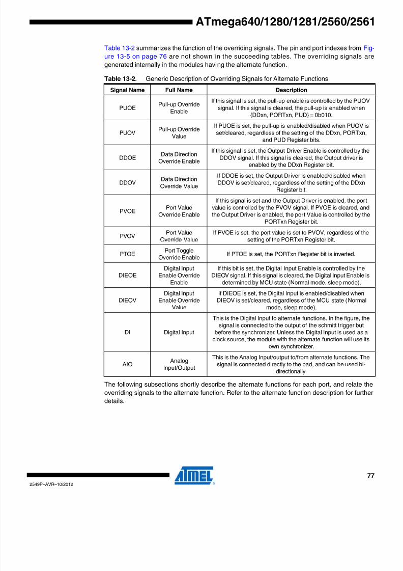
8/20/2019 At Mega 1281 Unlocked
http://slidepdf.com/reader/full/at-mega-1281-unlocked 77/446
77
2549P–AVR–10/2012
ATmega640/1280/1281/2560/2561
Table 13-2 summarizes the function of the overriding signals. The pin and port indexes from Fig
ure 13-5 on page 76 are not shown in the succeeding tables. The overriding signals are
generated internally in the modules having the alternate function.
The following subsections shortly describe the alternate functions for each port, and relate the
overriding signals to the alternate function. Refer to the alternate function description for furtherdetails.
Table 13-2. Generic Description of Overriding Signals for Alternate Functions
Signal Name Full Name Description
PUOEPull-up Override
Enable
If this signal is set, the pull-up enable is controlled by the PUOVsignal. If this signal is cleared, the pull-up is enabled when
{DDxn, PORTxn, PUD} = 0b010.
PUOVPull-up Override
Value
If PUOE is set, the pull-up is enabled/disabled when PUOV isset/cleared, regardless of the setting of the DDxn, PORTxn,
and PUD Register bits.
DDOEData Direction
Override Enable
If this signal is set, the Output Driver Enable is controlled by theDDOV signal. If this signal is cleared, the Output driver is
enabled by the DDxn Register bit.
DDOVData DirectionOverride Value
If DDOE is set, the Output Driver is enabled/disabled whenDDOV is set/cleared, regardless of the setting of the DDxn
Register bit.
PVOEPort Value
Override Enable
If this signal is set and the Output Driver is enabled, the portvalue is controlled by the PVOV signal. If PVOE is cleared, andthe Output Driver is enabled, the port Value is controlled by the
PORTxn Register bit.
PVOVPort Value
Override ValueIf PVOE is set, the port value is set to PVOV, regardless of the
setting of the PORTxn Register bit.
PTOEPort Toggle
Override EnableIf PTOE is set, the PORTxn Register bit is inverted.
DIEOEDigital Input
Enable OverrideEnable
If this bit is set, the Digital Input Enable is controlled by theDIEOV signal. If this signal is cleared, the Digital Input Enable is
determined by MCU state (Normal mode, sleep mode).
DIEOVDigital Input
Enable OverrideValue
If DIEOE is set, the Digital Input is enabled/disabled whenDIEOV is set/cleared, regardless of the MCU state (Normal
mode, sleep mode).
DI Digital Input
This is the Digital Input to alternate functions. In the figure, thesignal is connected to the output of the schmitt trigger but
before the synchronizer. Unless the Digital Input is used as aclock source, the module with the alternate function will use its
own synchronizer.
AIOAnalog
Input/Output
This is the Analog Input/output to/from alternate functions. Thesignal is connected directly to the pad, and can be used bi-
directionally.

8/20/2019 At Mega 1281 Unlocked
http://slidepdf.com/reader/full/at-mega-1281-unlocked 78/446
78
2549P–AVR–10/2012
ATmega640/1280/1281/2560/2561
13.3.1 Alternate Functions of Port A
The Port A has an alternate function as the address low byte and data lines for the Externa
Memory Interface.
Table 13-4 and Table 13-5 on page 79 relates the alternate functions of Port A to the overridingsignals shown in Figure 13-5 on page 76.
Note: 1. ADA is short for ADdress Active and represents the time when address is output. See “Exter-nal Memory Interface” on page 28 for details.
Table 13-3. Port A Pins Alternate Functions
Port Pin Alternate Function
PA7 AD7 (External memory interface address and data bit 7)
PA6 AD6 (External memory interface address and data bit 6)
PA5 AD5 (External memory interface address and data bit 5)
PA4 AD4 (External memory interface address and data bit 4)
PA3 AD3 (External memory interface address and data bit 3)
PA2 AD2 (External memory interface address and data bit 2)
PA1 AD1 (External memory interface address and data bit 1)
PA0 AD0 (External memory interface address and data bit 0)
Table 13-4. Overriding Signals for Alternate Functions in PA7:PA4
Signal
Name PA7/AD7 PA6/AD6 PA5/AD5 PA4/AD4
PUOE SRE SRE SRE SRE
PUOV~(WR | ADA(1)) •PORTA7 • PUD
~(WR | ADA) •PORTA6 • PUD
~(WR | ADA) •PORTA5 • PUD
~(WR | ADA) •PORTA4 • PUD
DDOE SRE SRE SRE SRE
DDOV WR | ADA WR | ADA WR | ADA WR | ADA
PVOE SRE SRE SRE SRE
PVOVA7 • ADA | D7OUTPUT • WR
A6 • ADA | D6OUTPUT • WR
A5 • ADA | D5OUTPUT • WR
A4 • ADA | D4OUTPUT • WR
DIEOE 0 0 0 0
DIEOV 0 0 0 0
DI D7 INPUT D6 INPUT D5 INPUT D4 INPUT
AIO – – – –
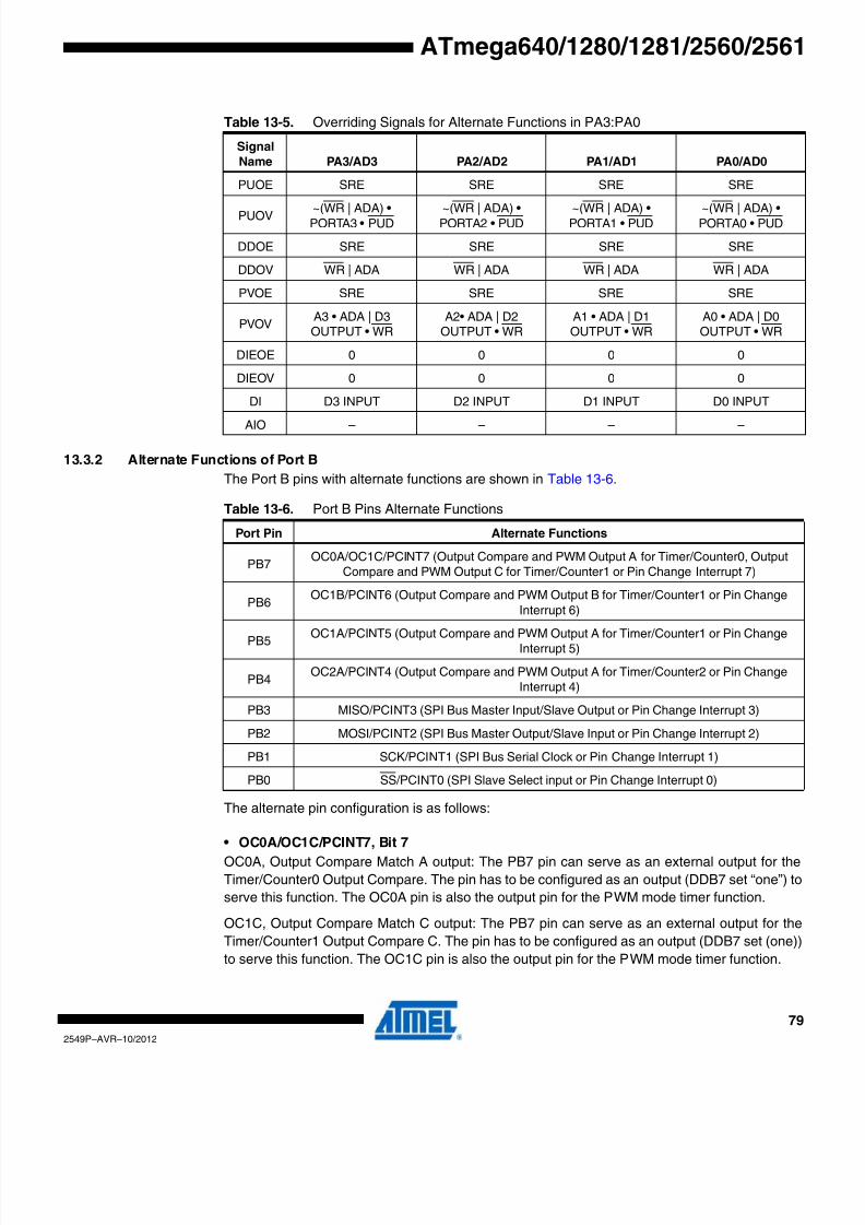
8/20/2019 At Mega 1281 Unlocked
http://slidepdf.com/reader/full/at-mega-1281-unlocked 79/446
79
2549P–AVR–10/2012
ATmega640/1280/1281/2560/2561
13.3.2 Alternate Functions of Port B
The Port B pins with alternate functions are shown in Table 13-6.
The alternate pin configuration is as follows:
• OC0A/OC1C/PCINT7, Bit 7
OC0A, Output Compare Match A output: The PB7 pin can serve as an external output for the
Timer/Counter0 Output Compare. The pin has to be configured as an output (DDB7 set “one”) to
serve this function. The OC0A pin is also the output pin for the PWM mode timer function.
OC1C, Output Compare Match C output: The PB7 pin can serve as an external output for the
Timer/Counter1 Output Compare C. The pin has to be configured as an output (DDB7 set (one)
to serve this function. The OC1C pin is also the output pin for the PWM mode timer function.
Table 13-5. Overriding Signals for Alternate Functions in PA3:PA0
Signal
Name PA3/AD3 PA2/AD2 PA1/AD1 PA0/AD0
PUOE SRE SRE SRE SRE
PUOV ~(WR | ADA) •PORTA3 • PUD
~(WR | ADA) •PORTA2 • PUD
~(WR | ADA) •PORTA1 • PUD
~(WR | ADA) •PORTA0 • PUD
DDOE SRE SRE SRE SRE
DDOV WR | ADA WR | ADA WR | ADA WR | ADA
PVOE SRE SRE SRE SRE
PVOVA3 • ADA | D3OUTPUT • WR
A2• ADA | D2OUTPUT • WR
A1 • ADA | D1OUTPUT • WR
A0 • ADA | D0OUTPUT • WR
DIEOE 0 0 0 0
DIEOV 0 0 0 0
DI D3 INPUT D2 INPUT D1 INPUT D0 INPUT
AIO – – – –
Table 13-6. Port B Pins Alternate Functions
Port Pin Alternate Functions
PB7OC0A/OC1C/PCINT7 (Output Compare and PWM Output A for Timer/Counter0, Output
Compare and PWM Output C for Timer/Counter1 or Pin Change Interrupt 7)
PB6OC1B/PCINT6 (Output Compare and PWM Output B for Timer/Counter1 or Pin Change
Interrupt 6)
PB5OC1A/PCINT5 (Output Compare and PWM Output A for Timer/Counter1 or Pin Change
Interrupt 5)
PB4OC2A/PCINT4 (Output Compare and PWM Output A for Timer/Counter2 or Pin Change
Interrupt 4)
PB3 MISO/PCINT3 (SPI Bus Master Input/Slave Output or Pin Change Interrupt 3)
PB2 MOSI/PCINT2 (SPI Bus Master Output/Slave Input or Pin Change Interrupt 2)
PB1 SCK/PCINT1 (SPI Bus Serial Clock or Pin Change Interrupt 1)
PB0 SS/PCINT0 (SPI Slave Select input or Pin Change Interrupt 0)
8/20/2019 At Mega 1281 Unlocked
http://slidepdf.com/reader/full/at-mega-1281-unlocked 80/446
80
2549P–AVR–10/2012
ATmega640/1280/1281/2560/2561
PCINT7, Pin Change Interrupt source 7: The PB7 pin can serve as an external interrupt source.
• OC1B/PCINT6, Bit 6
OC1B, Output Compare Match B output: The PB6 pin can serve as an external output for the
Timer/Counter1 Output Compare B. The pin has to be configured as an output (DDB6 set (one)
to serve this function. The OC1B pin is also the output pin for the PWM mode timer function.
PCINT6, Pin Change Interrupt source 6: The PB6 pin can serve as an external interrupt source.
• OC1A/PCINT5, Bit 5
OC1A, Output Compare Match A output: The PB5 pin can serve as an external output for the
Timer/Counter1 Output Compare A. The pin has to be configured as an output (DDB5 set (one)
to serve this function. The OC1A pin is also the output pin for the PWM mode timer function.
PCINT5, Pin Change Interrupt source 5: The PB5 pin can serve as an external interrupt source.
• OC2A/PCINT4, Bit 4
OC2A, Output Compare Match output: The PB4 pin can serve as an external output for the
Timer/Counter2 Output Compare. The pin has to be configured as an output (DDB4 set (one)) to
serve this function. The OC2A pin is also the output pin for the PWM mode timer function.
PCINT4, Pin Change Interrupt source 4: The PB4 pin can serve as an external interrupt source.
• MISO/PCINT3 – Port B, Bit 3
MISO: Master Data input, Slave Data output pin for SPI channel. When the SPI is enabled as a
master, this pin is configured as an input regardless of the setting of DDB3. When the SPI is
enabled as a slave, the data direction of this pin is controlled by DDB3. When the pin is forced to
be an input, the pull-up can still be controlled by the PORTB3 bit.
PCINT3, Pin Change Interrupt source 3: The PB3 pin can serve as an external interrupt source.
• MOSI/PCINT2 – Port B, Bit 2
MOSI: SPI Master Data output, Slave Data input for SPI channel. When the SPI is enabled as aslave, this pin is configured as an input regardless of the setting of DDB2. When the SPI is
enabled as a master, the data direction of this pin is controlled by DDB2. When the pin is forced
to be an input, the pull-up can still be controlled by the PORTB2 bit.
PCINT2, Pin Change Interrupt source 2: The PB2 pin can serve as an external interrupt source.
• SCK/PCINT1 – Port B, Bit 1
SCK: Master Clock output, Slave Clock input pin for SPI channel. When the SPI is enabled as a
slave, this pin is configured as an input regardless of the setting of DDB1. When the SPI0 is
enabled as a master, the data direction of this pin is controlled by DDB1. When the pin is forced
to be an input, the pull-up can still be controlled by the PORTB1 bit.
PCINT1, Pin Change Interrupt source 1: The PB1 pin can serve as an external interrupt source.
• SS/PCINT0 – Port B, Bit 0
SS: Slave Port Select input. When the SPI is enabled as a slave, this pin is configured as an
input regardless of the setting of DDB0. As a slave, the SPI is activated when this pin is driven
low. When the SPI is enabled as a master, the data direction of this pin is controlled by DDB0
When the pin is forced to be an input, the pull-up can still be controlled by the PORTB0 bit.

8/20/2019 At Mega 1281 Unlocked
http://slidepdf.com/reader/full/at-mega-1281-unlocked 81/446
81
2549P–AVR–10/2012
ATmega640/1280/1281/2560/2561
Table 13-7 and Table 13-8 relate the alternate functions of Port B to the overriding signals
shown in Figure 13-5 on page 76. SPI MSTR INPUT and SPI SLAVE OUTPUT constitute the
MISO signal, while MOSI is divided into SPI MSTR OUTPUT and SPI SLAVE INPUT.
PCINT0, Pin Change Interrupt source 0: The PB0 pin can serve as an external interrupt source.
Table 13-7. Overriding Signals for Alternate Functions in PB7:PB4
Signal
Name PB7/OC0A/OC1C PB6/OC1B PB5/OC1A PB4/OC2A
PUOE 0 0 0 0
PUOV 0 0 0 0
DDOE 0 0 0 0
DDOV 0 0 0 0
PVOE OC0/OC1C ENABLE OC1B ENABLE OC1A ENABLE OC2A ENABLE
PVOV OC0/OC1C OC1B OC1A OC2A
DIEOE PCINT7 • PCIE0 PCINT6 • PCIE0 PCINT5 • PCIE0 PCINT4 • PCIE0
DIEOV 1 1 1 1
DI PCINT7 INPUT PCINT6 INPUT PCINT5 INPUT PCINT4 INPUT
AIO – – – –
Table 13-8. Overriding Signals for Alternate Functions in PB3:PB0
Signal
Name PB3/MISO PB2/MOSI PB1/SCK PB0/SS
PUOE SPE • MSTR SPE • MSTR SPE • MSTR SPE • MSTR
PUOV PORTB3 • PUD PORTB2 • PUD PORTB1 • PUD PORTB0 • PUD
DDOE SPE • MSTR SPE • MSTR SPE • MSTR SPE • MSTR
DDOV 0 0 0 0
PVOE SPE • MSTR SPE • MSTR SPE • MSTR 0
PVOV SPI SLAVE OUTPUT SPI MSTR OUTPUT SCK OUTPUT 0
DIEOE PCINT3 • PCIE0 PCINT2 • PCIE0 PCINT1 • PCIE0 PCINT0 • PCIE0
DIEOV 1 1 1 1
DISPI MSTR INPUT
PCINT3 INPUT
SPI SLAVE INPUT
PCINT2 INPUT
SCK INPUT
PCINT1 INPUT
SPI SS
PCINT0 INPUT
AIO – – – –

8/20/2019 At Mega 1281 Unlocked
http://slidepdf.com/reader/full/at-mega-1281-unlocked 82/446
82
2549P–AVR–10/2012
ATmega640/1280/1281/2560/2561
13.3.3 Alternate Functions of Port C
The Port C alternate function is as follows:
Table 13-10 and Table 13-11 on page 83 relate the alternate functions of Port C to the overriding
signals shown in Figure 13-5 on page 76.
Table 13-9. Port C Pins Alternate FunctionsPort Pin Alternate Function
PC7 A15 (External Memory interface address bit 15)
PC6 A14 (External Memory interface address bit 14)
PC5 A13 (External Memory interface address bit 13)
PC4 A12 (External Memory interface address bit 12)
PC3 A11 (External Memory interface address bit 11)
PC2 A10 (External Memory interface address bit 10)
PC1 A9 (External Memory interface address bit 9)
PC0 A8 (External Memory interface address bit 8)
Table 13-10. Overriding Signals for Alternate Functions in PC7:PC4
Signal
Name PC7/A15 PC6/A14 PC5/A13 PC4/A12
PUOE SRE • (XMM<1) SRE • (XMM<2) SRE • (XMM<3) SRE • (XMM<4)
PUOV 0 0 0 0
DDOE SRE • (XMM<1) SRE • (XMM<2) SRE • (XMM<3) SRE • (XMM<4)
DDOV 1 1 1 1
PVOE SRE • (XMM<1) SRE • (XMM<2) SRE • (XMM<3) SRE • (XMM<4)
PVOV A15 A14 A13 A12
DIEOE 0 0 0 0
DIEOV 0 0 0 0
DI – – – –
AIO – – – –

8/20/2019 At Mega 1281 Unlocked
http://slidepdf.com/reader/full/at-mega-1281-unlocked 83/446
83
2549P–AVR–10/2012
ATmega640/1280/1281/2560/2561
13.3.4 Alternate Functions of Port D
The Port D pins with alternate functions are shown in Table 13-12.
The alternate pin configuration is as follows:
• T0 – Port D, Bit 7
T0, Timer/Counter0 counter source.
• T1 – Port D, Bit 6
T1, Timer/Counter1 counter source.
• XCK1 – Port D, Bit 5
XCK1, USART1 External clock. The Data Direction Register (DDD5) controls whether the clock
is output (DDD5 set) or input (DDD5 cleared). The XCK1 pin is active only when the USART1
operates in Synchronous mode.
• ICP1 – Port D, Bit 4
ICP1 – Input Capture Pin 1: The PD4 pin can act as an input capture pin for Timer/Counter1.
Table 13-11. Overriding Signals for Alternate Functions in PC3:PC0
Signal
Name PC3/A11 PC2/A10 PC1/A9 PC0/A8
PUOE SRE • (XMM<5) SRE • (XMM<6) SRE • (XMM<7) SRE • (XMM<7)
PUOV 0 0 0 0
DDOE SRE • (XMM<5) SRE • (XMM<6) SRE • (XMM<7) SRE • (XMM<7)
DDOV 1 1 1 1
PVOE SRE • (XMM<5) SRE • (XMM<6) SRE • (XMM<7) SRE • (XMM<7)
PVOV A11 A10 A9 A8
DIEOE 0 0 0 0
DIEOV 0 0 0 0
DI – – – –
AIO – – – –
Table 13-12. Port D Pins Alternate Functions
Port Pin Alternate Function
PD7 T0 (Timer/Counter0 Clock Input)
PD6 T1 (Timer/Counter1 Clock Input)
PD5 XCK1 (USART1 External Clock Input/Output)
PD4 ICP1 (Timer/Counter1 Input Capture Trigger)
PD3 INT3/TXD1 (External Interrupt3 Input or USART1 Transmit Pin)
PD2 INT2/RXD1 (External Interrupt2 Input or USART1 Receive Pin)
PD1 INT1/SDA (External Interrupt1 Input or TWI Serial DAta)
PD0 INT0/SCL (External Interrupt0 Input or TWI Serial CLock)
8/20/2019 At Mega 1281 Unlocked
http://slidepdf.com/reader/full/at-mega-1281-unlocked 84/446
84
2549P–AVR–10/2012
ATmega640/1280/1281/2560/2561
• INT3/TXD1 – Port D, Bit 3
INT3, External Interrupt source 3: The PD3 pin can serve as an external interrupt source to the
MCU.
TXD1, Transmit Data (Data output pin for the USART1). When the USART1 Transmitter is
enabled, this pin is configured as an output regardless of the value of DDD3.
• INT2/RXD1 – Port D, Bit 2
INT2, External Interrupt source 2. The PD2 pin can serve as an External Interrupt source to the
MCU.
RXD1, Receive Data (Data input pin for the USART1). When the USART1 receiver is enabled
this pin is configured as an input regardless of the value of DDD2. When the USART forces this
pin to be an input, the pull-up can still be controlled by the PORTD2 bit.
• INT1/SDA – Port D, Bit 1
INT1, External Interrupt source 1. The PD1 pin can serve as an external interrupt source to the
MCU.
SDA, 2-wire Serial Interface Data: When the TWEN bit in TWCR is set (one) to enable the 2-wireSerial Interface, pin PD1 is disconnected from the port and becomes the Serial Data I/O pin fo
the 2-wire Serial Interface. In this mode, there is a spike filter on the pin to suppress spikes
shorter than 50ns on the input signal, and the pin is driven by an open drain driver with slew-rate
limitation.
• INT0/SCL – Port D, Bit 0
INT0, External Interrupt source 0. The PD0 pin can serve as an external interrupt source to the
MCU.
SCL, 2-wire Serial Interface Clock: When the TWEN bit in TWCR is set (one) to enable the 2-
wire Serial Interface, pin PD0 is disconnected from the port and becomes the Serial Clock I/O
pin for the 2-wire Serial Interface. In this mode, there is a spike filter on the pin to suppress
spikes shorter than 50ns on the input signal, and the pin is driven by an open drain driver with
slew-rate limitation.
Table 13-13 on page 85 and Table 13-14 on page 85 relates the alternate functions of Port D to
the overriding signals shown in Figure 13-5 on page 76.

8/20/2019 At Mega 1281 Unlocked
http://slidepdf.com/reader/full/at-mega-1281-unlocked 85/446
85
2549P–AVR–10/2012
ATmega640/1280/1281/2560/2561
Note: 1. When enabled, the 2-wire Serial Interface enables Slew-Rate controls on the output pins PD0and PD1. This is not shown in this table. In addition, spike filters are connected between theAIO outputs shown in the port figure and the digital logic of the TWI module.
Table 13-13. Overriding Signals for Alternate Functions PD7:PD4
Signal Name PD7/T0 PD6/T1 PD5/XCK1 PD4/ICP1
PUOE 0 0 0 0
PUOV 0 0 0 0
DDOE 0 0 XCK1 OUTPUT ENABLE 0
DDOV 0 0 1 0
PVOE 0 0 XCK1 OUTPUT ENABLE 0
PVOV 0 0 XCK1 OUTPUT 0
DIEOE 0 0 0 0
DIEOV 0 0 0 0
DI T0 INPUT T1 INPUT XCK1 INPUT ICP1 INPUT
AIO – – – –
Table 13-14. Overriding Signals for Alternate Functions in PD3:PD0(1)
Signal Name PD3/INT3/TXD1 PD2/INT2/RXD1 PD1/INT1/SDA PD0/INT0/SCL
PUOE TXEN1 RXEN1 TWEN TWEN
PUOV 0 PORTD2 • PUD PORTD1 • PUD PORTD0 • PUD
DDOE TXEN1 RXEN1 TWEN TWEN
DDOV 1 0 SDA_OUT SCL_OUT
PVOE TXEN1 0 TWEN TWEN
PVOV TXD1 0 0 0
DIEOE INT3 ENABLE INT2 ENABLE INT1 ENABLE INT0 ENABLE
DIEOV 1 1 1 1
DI INT3 INPUT INT2 INPUT/RXD1 INT1 INPUT INT0 INPUT
AIO – – SDA INPUT SCL INPUT
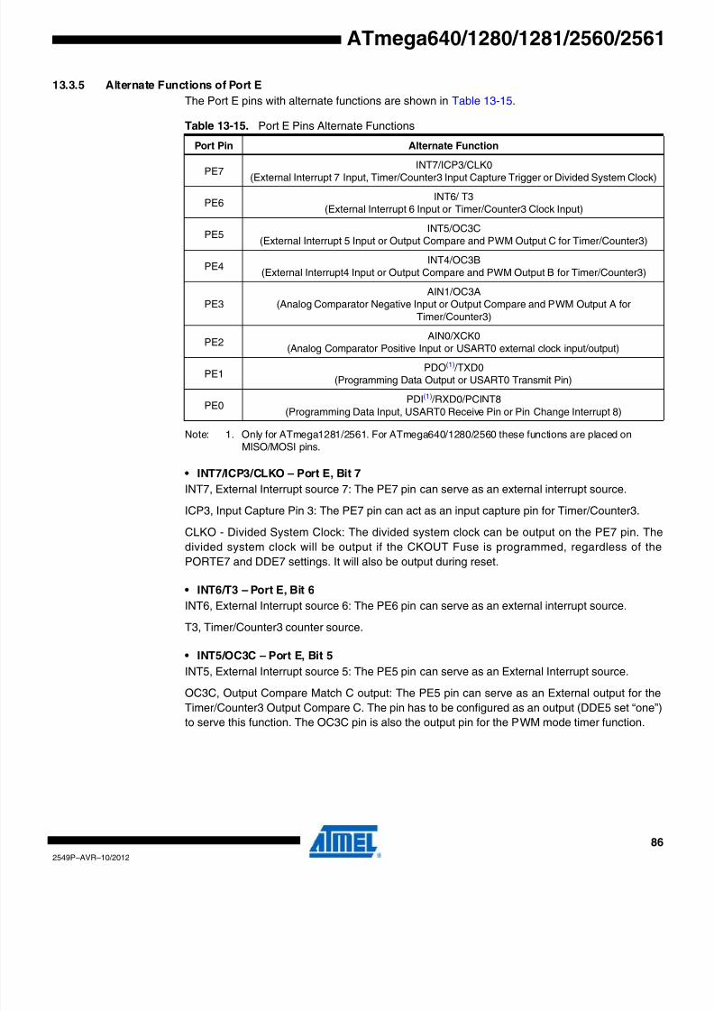
8/20/2019 At Mega 1281 Unlocked
http://slidepdf.com/reader/full/at-mega-1281-unlocked 86/446
86
2549P–AVR–10/2012
ATmega640/1280/1281/2560/2561
13.3.5 Alternate Functions of Port E
The Port E pins with alternate functions are shown in Table 13-15.
Note: 1. Only for ATmega1281/2561. For ATmega640/1280/2560 these functions are placed onMISO/MOSI pins.
• INT7/ICP3/CLKO – Port E, Bit 7
INT7, External Interrupt source 7: The PE7 pin can serve as an external interrupt source.
ICP3, Input Capture Pin 3: The PE7 pin can act as an input capture pin for Timer/Counter3.
CLKO - Divided System Clock: The divided system clock can be output on the PE7 pin. The
divided system clock will be output if the CKOUT Fuse is programmed, regardless of the
PORTE7 and DDE7 settings. It will also be output during reset.
• INT6/T3 – Port E, Bit 6
INT6, External Interrupt source 6: The PE6 pin can serve as an external interrupt source.
T3, Timer/Counter3 counter source.
• INT5/OC3C – Port E, Bit 5
INT5, External Interrupt source 5: The PE5 pin can serve as an External Interrupt source.
OC3C, Output Compare Match C output: The PE5 pin can serve as an External output for theTimer/Counter3 Output Compare C. The pin has to be configured as an output (DDE5 set “one”
to serve this function. The OC3C pin is also the output pin for the PWM mode timer function.
Table 13-15. Port E Pins Alternate Functions
Port Pin Alternate Function
PE7INT7/ICP3/CLK0
(External Interrupt 7 Input, Timer/Counter3 Input Capture Trigger or Divided System Clock)
PE6INT6/ T3
(External Interrupt 6 Input or Timer/Counter3 Clock Input)
PE5INT5/OC3C
(External Interrupt 5 Input or Output Compare and PWM Output C for Timer/Counter3)
PE4INT4/OC3B
(External Interrupt4 Input or Output Compare and PWM Output B for Timer/Counter3)
PE3AIN1/OC3A
(Analog Comparator Negative Input or Output Compare and PWM Output A forTimer/Counter3)
PE2
AIN0/XCK0
(Analog Comparator Positive Input or USART0 external clock input/output)
PE1PDO(1) /TXD0
(Programming Data Output or USART0 Transmit Pin)
PE0PDI(1) /RXD0/PCINT8
(Programming Data Input, USART0 Receive Pin or Pin Change Interrupt 8)

8/20/2019 At Mega 1281 Unlocked
http://slidepdf.com/reader/full/at-mega-1281-unlocked 87/446
87
2549P–AVR–10/2012
ATmega640/1280/1281/2560/2561
• INT4/OC3B – Port E, Bit 4
INT4, External Interrupt source 4: The PE4 pin can serve as an External Interrupt source.
OC3B, Output Compare Match B output: The PE4 pin can serve as an External output for the
Timer/Counter3 Output Compare B. The pin has to be configured as an output (DDE4 set (one)
to serve this function. The OC3B pin is also the output pin for the PWM mode timer function.
• AIN1/OC3A – Port E, Bit 3
AIN1 – Analog Comparator Negative input. This pin is directly connected to the negative input o
the Analog Comparator.
OC3A, Output Compare Match A output: The PE3 pin can serve as an External output for the
Timer/Counter3 Output Compare A. The pin has to be configured as an output (DDE3 set “one”
to serve this function. The OC3A pin is also the output pin for the PWM mode timer function.
• AIN0/XCK0 – Port E, Bit 2
AIN0 – Analog Comparator Positive input. This pin is directly connected to the positive input of
the Analog Comparator.
XCK0, USART0 External clock. The Data Direction Register (DDE2) controls whether the clock
is output (DDE2 set) or input (DDE2 cleared). The XCK0 pin is active only when the USART0
operates in Synchronous mode.
• PDO/TXD0 – Port E, Bit 1
PDO, SPI Serial Programming Data Output. During Serial Program Downloading, this pin is
used as data output line for the ATmega1281/2561. For ATmega640/1280/2560 this function is
placed on MISO.
TXD0, USART0 Transmit pin.
• PDI/RXD0/PCINT8 – Port E, Bit 0
PDI, SPI Serial Programming Data Input. During Serial Program Downloading, this pin is used
as data input line for the ATmega1281/2561. For ATmega640/1280/2560 this function is placed
on MOSI.
RXD0, USART0 Receive Pin. Receive Data (Data input pin for the USART0). When the
USART0 receiver is enabled this pin is configured as an input regardless of the value of DDRE0
When the USART0 forces this pin to be an input, a logical one in PORTE0 will turn on the inter-
nal pull-up.
PCINT8, Pin Change Interrupt source 8: The PE0 pin can serve as an external interrupt source.
Table 13-16 on page 88 and Table 13-17 on page 88 relates the alternate functions of Port E to
the overriding signals shown in Figure 13-5 on page 76.

8/20/2019 At Mega 1281 Unlocked
http://slidepdf.com/reader/full/at-mega-1281-unlocked 88/446
88
2549P–AVR–10/2012
ATmega640/1280/1281/2560/2561
Note: 1. PDO/PDI only available at PE1/PE0 for ATmega1281/2561.
Table 13-16. Overriding Signals for Alternate Functions PE7:PE4
Signal
Name PE7/INT7/ICP3 PE6/INT6/T3 PE5/INT5/OC3C PE4/INT4/OC3B
PUOE 0 0 0 0
PUOV 0 0 0 0
DDOE 0 0 0 0
DDOV 0 0 0 0
PVOE 0 0 OC3C ENABLE OC3B ENABLE
PVOV 0 0 OC3C OC3B
DIEOE INT7 ENABLE INT6 ENABLE INT5 ENABLE INT4 ENABLE
DIEOV 1 1 1 1
DIINT7 INPUT/ICP3
INPUTINT7 INPUT/T3
INPUTINT5 INPUT INT4 INPUT
AIO – – – –
Table 13-17. Overriding Signals for Alternate Functions in PE3:PE0
Signal
Name PE3/AIN1/OC3A PE2/AIN0/XCK0
PE1/PDO(1) /
TXD0
PE0/PDI(1) /
RXD0/PCINT8
PUOE 0 0 TXEN0 RXEN0
PUOV 0 0 0 PORTE0 • PUD
DDOE 0XCK0 OUTPUT
ENABLETXEN0 RXEN0
DDOV 0 1 1 0
PVOE OC3B ENABLEXCK0 OUTPUT
ENABLETXEN0 0
PVOV OC3B XCK0 OUTPUT TXD0 0
DIEOE 0 0 0 PCINT8 • PCIE1
DIEOV 0 0 0 1
DI 0 XCK0 INPUT – RXD0
PE0 0 0 0 PCINT8 INPUT
AIO AIN1 INPUT AIN0 INPUT – –
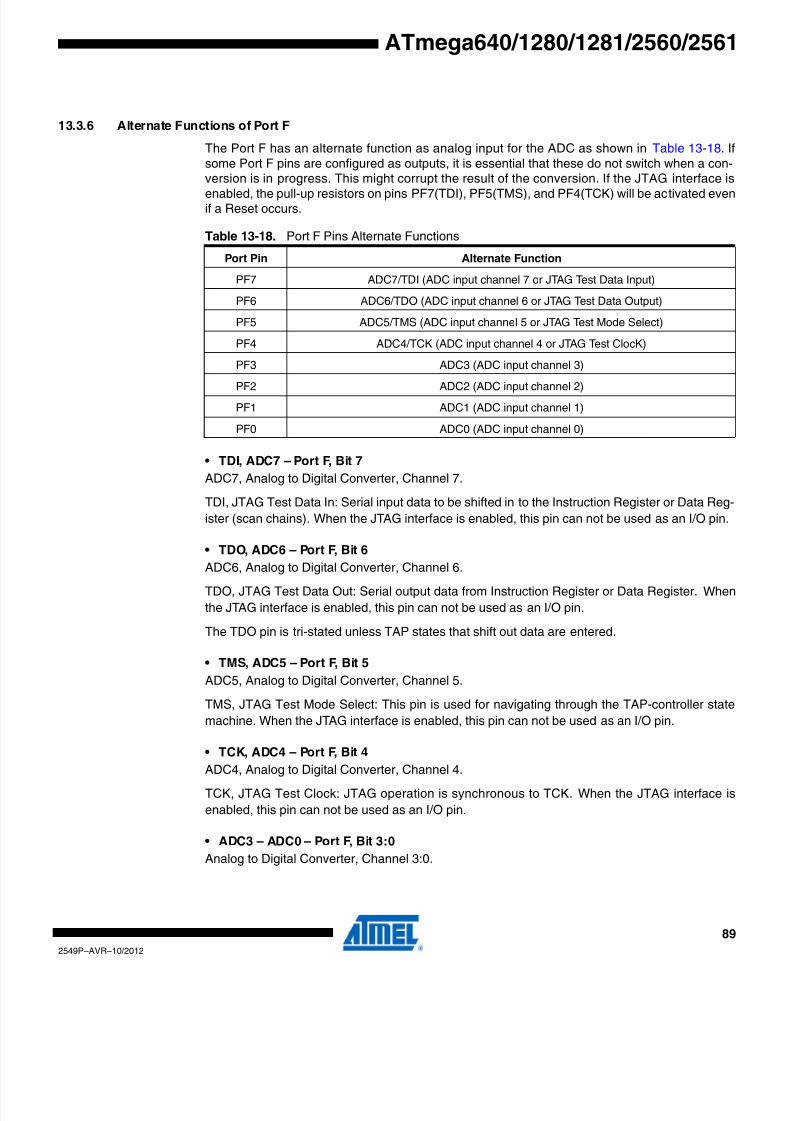
8/20/2019 At Mega 1281 Unlocked
http://slidepdf.com/reader/full/at-mega-1281-unlocked 89/446
89
2549P–AVR–10/2012
ATmega640/1280/1281/2560/2561
13.3.6 Alternate Functions of Port F
The Port F has an alternate function as analog input for the ADC as shown in Table 13-18. Ifsome Port F pins are configured as outputs, it is essential that these do not switch when a con-version is in progress. This might corrupt the result of the conversion. If the JTAG interface is
enabled, the pull-up resistors on pins PF7(TDI), PF5(TMS), and PF4(TCK) will be activated evenif a Reset occurs.
• TDI, ADC7 – Port F, Bit 7
ADC7, Analog to Digital Converter, Channel 7.
TDI, JTAG Test Data In: Serial input data to be shifted in to the Instruction Register or Data Reg
ister (scan chains). When the JTAG interface is enabled, this pin can not be used as an I/O pin.
• TDO, ADC6 – Port F, Bit 6
ADC6, Analog to Digital Converter, Channel 6.
TDO, JTAG Test Data Out: Serial output data from Instruction Register or Data Register. When
the JTAG interface is enabled, this pin can not be used as an I/O pin.
The TDO pin is tri-stated unless TAP states that shift out data are entered.
• TMS, ADC5 – Port F, Bit 5
ADC5, Analog to Digital Converter, Channel 5.
TMS, JTAG Test Mode Select: This pin is used for navigating through the TAP-controller state
machine. When the JTAG interface is enabled, this pin can not be used as an I/O pin.
• TCK, ADC4 – Port F, Bit 4
ADC4, Analog to Digital Converter, Channel 4.
TCK, JTAG Test Clock: JTAG operation is synchronous to TCK. When the JTAG interface is
enabled, this pin can not be used as an I/O pin.
• ADC3 – ADC0 – Port F, Bit 3:0
Analog to Digital Converter, Channel 3:0.
Table 13-18. Port F Pins Alternate Functions
Port Pin Alternate Function
PF7 ADC7/TDI (ADC input channel 7 or JTAG Test Data Input)
PF6 ADC6/TDO (ADC input channel 6 or JTAG Test Data Output)
PF5 ADC5/TMS (ADC input channel 5 or JTAG Test Mode Select)
PF4 ADC4/TCK (ADC input channel 4 or JTAG Test ClocK)
PF3 ADC3 (ADC input channel 3)
PF2 ADC2 (ADC input channel 2)
PF1 ADC1 (ADC input channel 1)
PF0 ADC0 (ADC input channel 0)

8/20/2019 At Mega 1281 Unlocked
http://slidepdf.com/reader/full/at-mega-1281-unlocked 90/446
90
2549P–AVR–10/2012
ATmega640/1280/1281/2560/2561
13.3.7 Alternate Functions of Port G
The Port G alternate pin configuration is as follows:
Table 13-19. Overriding Signals for Alternate Functions in PF7:PF4
Signal
Name PF7/ADC7/TDI PF6/ADC6/TDO PF5/ADC5/TMS PF4/ADC4/TCK
PUOE JTAGEN JTAGEN JTAGEN JTAGEN
PUOV 1 0 1 1
DDOE JTAGEN JTAGEN JTAGEN JTAGEN
DDOV 0SHIFT_IR + SHIFT_DR
0 0
PVOE 0 JTAGEN 0 0
PVOV 0 TDO 0 0
DIEOE JTAGEN JTAGEN JTAGEN JTAGEN
DIEOV 0 0 0 0
DI – – – –
AIO TDI/ADC7 INPUT ADC6 INPUT TMS/ADC5 INPUT TCK/ADC4 INPUT
Table 13-20. Overriding Signals for Alternate Functions in PF3:PF0
Signal Name PF3/ADC3 PF2/ADC2 PF1/ADC1 PF0/ADC0
PUOE 0 0 0 0
PUOV 0 0 0 0
DDOE 0 0 0 0
DDOV 0 0 0 0
PVOE 0 0 0 0
PVOV 0 0 0 0
DIEOE 0 0 0 0
DIEOV 0 0 0 0
DI – – – –
AIO ADC3 INPUT ADC2 INPUT ADC1 INPUT ADC0 INPUT
Table 13-21. Port G Pins Alternate Functions
Port Pin Alternate FunctionPG5 OC0B (Output Compare and PWM Output B for Timer/Counter0)
PG4 TOSC1 (RTC Oscillator Timer/Counter2)
PG3 TOSC2 (RTC Oscillator Timer/Counter2)
PG2 ALE (Address Latch Enable to external memory)
PG1 RD (Read strobe to external memory)
PG0 WR (Write strobe to external memory)

8/20/2019 At Mega 1281 Unlocked
http://slidepdf.com/reader/full/at-mega-1281-unlocked 91/446
91
2549P–AVR–10/2012
ATmega640/1280/1281/2560/2561
• OC0B – Port G, Bit 5
OC0B, Output Compare match B output: The PG5 pin can serve as an external output for the
TImer/Counter0 Output Compare. The pin has to be configured as an output (DDG5 set) to
serve this function. The OC0B pin is also the output pin for the PWM mode timer function.
• TOSC1 – Port G, Bit 4
TOSC2, Timer Oscillator pin 1: When the AS2 bit in ASSR is set (one) to enable asynchronousclocking of Timer/Counter2, pin PG4 is disconnected from the port, and becomes the input of the
inverting Oscillator amplifier. In this mode, a Crystal Oscillator is connected to this pin, and the
pin can not be used as an I/O pin.
• TOSC2 – Port G, Bit 3
TOSC2, Timer Oscillator pin 2: When the AS2 bit in ASSR is set (one) to enable asynchronous
clocking of Timer/Counter2, pin PG3 is disconnected from the port, and becomes the inverting
output of the Oscillator amplifier. In this mode, a Crystal Oscillator is connected to this pin, and
the pin can not be used as an I/O pin.
• ALE – Port G, Bit 2
ALE is the external data memory Address Latch Enable signal.
• RD – Port G, Bit 1
RD is the external data memory read control strobe.
• WR – Port G, Bit 0
WR is the external data memory write control strobe.
Table 13-22 on page 91 and Table 13-23 on page 92 relates the alternate functions of Port G to
the overriding signals shown in Figure 13-5 on page 76.
Table 13-22. Overriding Signals for Alternate Functions in PG5:PG4
Signal Name — — PG5/OC0B PG4/TOSC1
PUOE – – – AS2
PUOV – – – 0
DDOE – – – AS2
DDOV – – – 0
PVOE – – OC0B Enable 0
PVOV – – OC0B 0
PTOE – – – –
DIEOE – – – AS2
DIEOV – – – EXCLK
DI – – – –
AIO – – – T/C2 OSC INPUT

8/20/2019 At Mega 1281 Unlocked
http://slidepdf.com/reader/full/at-mega-1281-unlocked 92/446
92
2549P–AVR–10/2012
ATmega640/1280/1281/2560/2561
13.3.8 Alternate Functions of Port H
The Port H alternate pin configuration is as follows:
• T4 – Port H, Bit 7
T4, Timer/Counter4 counter source.
• OC2B – Port H, Bit 6
OC2B, Output Compare Match B output: The PH6 pin can serve as an external output for the
Timer/Counter2 Output Compare B. The pin has to be configured as an output (DDH6 set) toserve this function. The OC2B pin is also the output pin for the PWM mode timer function.
• OC4C – Port H, Bit 5
OC4C, Output Compare Match C output: The PH5 pin can serve as an external output for the
Timer/Counter4 Output Compare C. The pin has to be configured as an output (DDH5 set) to
serve this function. The OC4C pin is also the output pin for the PWM mode timer function.
Table 13-23. Overriding Signals for Alternate Functions in PG3:PG0
Signal Name PG3/TOSC2 PG2/ALE/A7 PG1/RD PG0/WR
PUOE AS2 • EXCLK SRE SRE SRE
PUOV 0 0 0 0DDOE AS2 • EXCLK SRE SRE SRE
DDOV 0 1 1 1
PVOE 0 SRE SRE SRE
PVOV 0 ALE RD WR
PTOE – – – –
DIEOE AS2 • EXCLK 0 0 0
DIEOV 0 0 0 0
DI – – – –
AIO T/C2 OSC OUTPUT – – –
Table 13-24. Port H Pins Alternate Functions
Port Pin Alternate Function
PH7 T4 (Timer/Counter4 Clock Input)
PH6 OC2B (Output Compare and PWM Output B for Timer/Counter2)
PH5 OC4C (Output Compare and PWM Output C for Timer/Counter4)
PH4 OC4B (Output Compare and PWM Output B for Timer/Counter4)
PH3 OC4A (Output Compare and PWM Output A for Timer/Counter4)
PH2 XCK2 (USART2 External Clock)
PH1 TXD2 (USART2 Transmit Pin)
PH0 RXD2 (USART2 Receive Pin)

8/20/2019 At Mega 1281 Unlocked
http://slidepdf.com/reader/full/at-mega-1281-unlocked 93/446
93
2549P–AVR–10/2012
ATmega640/1280/1281/2560/2561
• OC4B – Port H, Bit 4
OC4B, Output Compare Match B output: The PH4 pin can serve as an external output for the
Timer/Counter2 Output Compare B. The pin has to be configured as an output (DDH4 set) to
serve this function. The OC4B pin is also the output pin for the PWM mode timer function.
• OC4A – Port H, Bit 3
OC4C, Output Compare Match A output: The PH3 pin can serve as an external output for theTimer/Counter4 Output Compare A. The pin has to be configured as an output (DDH3 set) to
serve this function. The OC4A pin is also the output pin for the PWM mode timer function.
• XCK2 – Port H, Bit 2
XCK2, USART2 External Clock: The Data Direction Register (DDH2) controls whether the clock
is output (DDH2 set) or input (DDH2 cleared). The XC2K pin is active only when the USART2
operates in synchronous mode.
• TXD2 – Port H, Bit 1
TXD2, USART2 Transmit Pin.
• RXD2 – Port H, Bit 0
RXD2, USART2 Receive pin: Receive Data (Data input pin for the USART2). When the
USART2 Receiver is enabled, this pin is configured as an input regardless of the value of DDH0
When the USART2 forces this pin to be an input, a logical on in PORTH0 will turn on the interna
pull-up.
Table 13-25. Overriding Signals for Alternate Functions in PH7:PH4
Signal Name PH7/T4 PH6/OC2B PH5/OC4C PH4/OC4B
PUOE 0 0 0 0
PUOV 0 0 0 0
DDOE 0 0 0 0
DDOV 0 0 0 0
PVOE 0 OC2B ENABLE OC4C ENABLE OC4B ENABLE
PVOV 0 OC2B OC4C OC4B
PTOE – – – –
DIEOE 0 0 0 0
DIEOV 0 0 0 0
DI T4 INPUT 0 0 0
AIO – – – –

8/20/2019 At Mega 1281 Unlocked
http://slidepdf.com/reader/full/at-mega-1281-unlocked 94/446
94
2549P–AVR–10/2012
ATmega640/1280/1281/2560/2561
13.3.9 Alternate Functions of Port J
The Port J alternate pin configuration is as follows:
• PCINT15:12 - Port J, Bit 6:3
PCINT15:12, Pin Change Interrupt Source 15:12. The PJ6:3 pins can serve as External Interrup
Sources.
• XCK2/PCINT11 - Port J, Bit 2
XCK2, USART 2 External Clock. The Data Direction Register (DDJ2) controls whether the clockis output (DDJ2 set) or input (DDJ2 cleared). The XCK2 pin is active only when the USART2
operates in synchronous mode.
PCINT11, Pin Change Interrupt Source 11. The PJ2 pin can serve as External Interrup
Sources.
Table 13-26. Overriding Signals for Alternate Functions in PH3:PH0
Signal Name PH3/OC4A PH2/XCK2 PH1/TXD2 PH0/RXD2
PUOE 0 0 TXEN2 RXEN2
PUOV 0 0 0 PORTH0 • PUD
DDOE 0
XCK2 OUTPUT
ENABLE TXEN
2 RXEN
2
DDOV 0 1 1 0
PVOE OC4A ENABLEXCK2 OUTPUT
ENABLETXEN2 0
PVOV OC4A XCK2 TXD2 0
PTOE – – – –
DIEOE 0 0 0 0
DIEOV 0 0 0 0
DI 0 XC2K INPUT 0 RXD2
AIO – – – –
Table 13-27. Port J Pins Alternate Functions
Port Pin Alternate Function
PJ7 –
PJ6 PCINT15 (Pin Change Interrupt 15)
PJ5 PCINT14 (Pin Change Interrupt 14)
PJ4 PCINT13 (Pin Change Interrupt 13)
PJ3 PCINT12 (Pin Change Interrupt 12)
PJ2 XCK3/PCINT11 (USART3 External Clock or Pin Change Interrupt 11)
PJ1 TXD3/PCINT10 (USART3 Transmit Pin or Pin Change Interrupt 10)
PJ0 RXD3/PCINT9 (USART3 Receive Pin or Pin Change Interrupt 9)

8/20/2019 At Mega 1281 Unlocked
http://slidepdf.com/reader/full/at-mega-1281-unlocked 95/446
95
2549P–AVR–10/2012
ATmega640/1280/1281/2560/2561
• TXD3/PCINT10 - Port J, Bit 1
TXD3, USART3 Transmit pin.
PCINT10, Pin Change Interrupt Source 10. The PJ1 pin can serve as External Interrup
Sources.
• RXD3/PCINT9 - Port J, Bit 0
RXD3, USART3 Receive pin. Receive Data (Data input pin for the USART3). When the
USART3 Receiver is enabled, this pin is configured as an input regardless of the value of DDJ0
When the USART3 forces this pin to be an input, a logical one in PORTJ0 will turn on the inter-
nal pull-up.
PCINT9, Pin Change Interrupt Source 9. The PJ0 pin can serve as External Interrupt Sources.
Table 13-28 on page 96 and Table 13-29 on page 96 relates the alternate functions of Port J to
the overriding signals shown in Figure 13-5 on page 76.

8/20/2019 At Mega 1281 Unlocked
http://slidepdf.com/reader/full/at-mega-1281-unlocked 96/446
96
2549P–AVR–10/2012
ATmega640/1280/1281/2560/2561
13.3.10 Alternate Functions of Port K
The Port K alternate pin configuration is as follows:
Table 13-28. Overriding Signals for Alternate Functions in PJ7:PJ4
Signal Name PJ7 PJ6/ PCINT15 PJ5/ PCINT14 PJ4/ PCINT13
PUOE 0 0 0 0
PUOV 0 0 0 0
DDOE 0 0 0 0
DDOV 0 0 0 0
PVOE 0 0 0 0
PVOV 0 0 0 0
PTOE - - - -
DIEOE 0 PCINT15·PCIE1 PCINT14·PCIE1 PCINT13·PCIE1
DIEOV 0 1 1 1
DI 0 PCINT15 INPUT PCINT14 INPUT PCINT13 INPUT
AIO - - - -
Table 13-29. Overriding Signals for Alternate Functions in PJ3:PJ0
Signal Name PJ3/PCINT12
PJ2/XCK3/PCINT
11
PJ1/TXD3/PCINT
10
PJ0/RXD3/PCINT
9
PUOE 0 0 TXEN3 RXEN3
PUOV 0 0 0 PORTJ0·PUD
DDOE 0 XCK3 OUTPUTENABLE
TXEN3 RXEN3
DDOV 0 1 1 0
PVOE 0 XCK3 OUTPUTENABLE
TXEN3 0
PVOV 0 XCK3 TXD3 0
PTOE - - - -
DIEOE PCINT12·PCIE1 PCINT11·PCIE1 PCINT10·PCIE1 PCINT9·PCIE1
DIEOV 1 1 1 1
DI PCINT12 INPUT PCINT11 INPUTXCK3 INPUT
PCINT10 INPUT PCINT9 INPUTRXD3
AIO - - - -
Table 13-30. Port K Pins Alternate Functions
Port Pin Alternate Function
PK7 ADC15/PCINT23 (ADC Input Channel 15 or Pin Change Interrupt 23)
PK6 ADC14/PCINT22 (ADC Input Channel 14 or Pin Change Interrupt 22)
PK5 ADC13/PCINT21 (ADC Input Channel 13 or Pin Change Interrupt 21)

8/20/2019 At Mega 1281 Unlocked
http://slidepdf.com/reader/full/at-mega-1281-unlocked 97/446
97
2549P–AVR–10/2012
ATmega640/1280/1281/2560/2561
• ADC15:8/PCINT23:16 – Port K, Bit 7:0
ADC15:8, Analog to Digital Converter, Channel 15 - 8.
PCINT23:16, Pin Change Interrupt Source 23:16. The PK7:0 pins can serve as External Inter-
rupt Sources.
PK4 ADC12/PCINT20 (ADC Input Channel 12 or Pin Change Interrupt 20)
PK3 ADC11/PCINT19 (ADC Input Channel 11 or Pin Change Interrupt 19)
PK2 ADC10/PCINT18 (ADC Input Channel 10 or Pin Change Interrupt 18)
PK1 ADC9/PCINT17 (ADC Input Channel 9 or Pin Change Interrupt 17)
PK0 ADC8 /PCINT16 (ADC Input Channel 8 or Pin Change Interrupt 16)
Table 13-31. Overriding Signals for Alternate Functions in PK7:PK4
Signal Name
PK7/ADC15/
PCINT23
PK6/ADC14/
PCINT22
PK5/ADC13/
PCINT21
PK4/ADC12/
PCINT20
PUOE 0 0 0 0
PUOV 0 0 0 0
DDOE 0 0 0 0
DDOV 0 0 0 0
PVOE 0 0 0 0
PVOV 0 0 0 0
PTOE – – – –
DIEOE PCINT23 • PCIE2 PCINT22 • PCIE2 PCINT21 • PCIE2 PCINT20 • PCIE2
DIEOV 1 1 1 1
DI PCINT23 INPUT PCINT22 INPUT PCINT21 INPUT PCINT20 INPUT
AIO ADC15 INPUT ADC14 INPUT ADC13 INPUT ADC12 INPUT
Table 13-30. Port K Pins Alternate Functions (Continued)
Port Pin Alternate Function
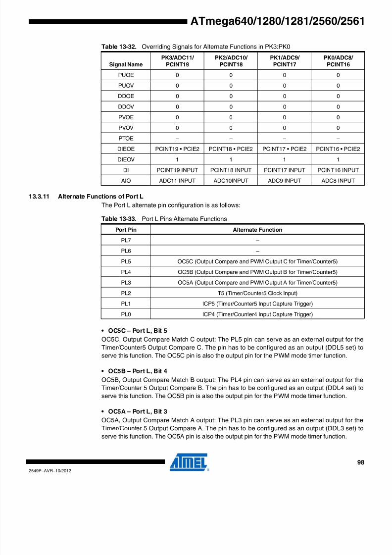
8/20/2019 At Mega 1281 Unlocked
http://slidepdf.com/reader/full/at-mega-1281-unlocked 98/446
98
2549P–AVR–10/2012
ATmega640/1280/1281/2560/2561
13.3.11 Alternate Functions of Port L
The Port L alternate pin configuration is as follows:
• OC5C – Port L, Bit 5
OC5C, Output Compare Match C output: The PL5 pin can serve as an external output for the
Timer/Counter5 Output Compare C. The pin has to be configured as an output (DDL5 set) to
serve this function. The OC5C pin is also the output pin for the PWM mode timer function.
• OC5B – Port L, Bit 4
OC5B, Output Compare Match B output: The PL4 pin can serve as an external output for theTimer/Counter 5 Output Compare B. The pin has to be configured as an output (DDL4 set) to
serve this function. The OC5B pin is also the output pin for the PWM mode timer function.
• OC5A – Port L, Bit 3
OC5A, Output Compare Match A output: The PL3 pin can serve as an external output for the
Timer/Counter 5 Output Compare A. The pin has to be configured as an output (DDL3 set) to
serve this function. The OC5A pin is also the output pin for the PWM mode timer function.
Table 13-32. Overriding Signals for Alternate Functions in PK3:PK0
Signal Name
PK3/ADC11/
PCINT19
PK2/ADC10/
PCINT18
PK1/ADC9/
PCINT17
PK0/ADC8/
PCINT16
PUOE 0 0 0 0
PUOV 0 0 0 0
DDOE 0 0 0 0
DDOV 0 0 0 0
PVOE 0 0 0 0
PVOV 0 0 0 0
PTOE – – – –
DIEOE PCINT19 • PCIE2 PCINT18 • PCIE2 PCINT17 • PCIE2 PCINT16 • PCIE2
DIEOV 1 1 1 1
DI PCINT19 INPUT PCINT18 INPUT PCINT17 INPUT PCINT16 INPUT
AIO ADC11 INPUT ADC10INPUT ADC9 INPUT ADC8 INPUT
Table 13-33. Port L Pins Alternate Functions
Port Pin Alternate Function
PL7 –
PL6 –
PL5 OC5C (Output Compare and PWM Output C for Timer/Counter5)
PL4 OC5B (Output Compare and PWM Output B for Timer/Counter5)
PL3 OC5A (Output Compare and PW
M Output A for Timer/Counter5)PL2 T5 (Timer/Counter5 Clock Input)
PL1 ICP5 (Timer/Counter5 Input Capture Trigger)
PL0 ICP4 (Timer/Counter4 Input Capture Trigger)

8/20/2019 At Mega 1281 Unlocked
http://slidepdf.com/reader/full/at-mega-1281-unlocked 99/446
99
2549P–AVR–10/2012
ATmega640/1280/1281/2560/2561
• T5 – Port L, Bit 2
T5, Timer/Counter5 counter source.
• ICP5 – Port L, Bit 1
ICP5, Input Capture Pin 5: The PL1 pin can serve as an Input Capture pin for Timer/Counter5.
• ICP4 – Port L, Bit 0ICP4, Input Capture Pin 4: The PL0 pin can serve as an Input Capture pin for Timer/Counter4.
Table 13-34 and Table 13-35 relates the alternate functions of Port L to the overriding signals
shown in Figure 13-5 on page 76.
Table 13-34. Overriding Signals for Alternate Functions in PL7:PL4
Signal Name PL7 PL6 PL5/OC5C PL4/OC5B
PUOE 0 0 0 0
PUOV 0 0 0 0
DDOE – – 0 0
DDOV – – 0 0
PVOE – – OC5C ENABLE OC5B ENABLE
PVOV – – OC5C OC5B
PTOE – – – –
DIEOE 0 0 0 0
DIEOV 0 0 0 0
DI 0 0 0 0
AIO – – – –
Table 13-35. Overriding Signals for Alternate Functions in PL3:PL0
Signal Name PL3/OC5A PL2/T5 PL1/ICP5 PL0/ICP4
PUOE 0 0 0 0
PUOV 0 0 0 0
DDOE 0 0 0 0
DDOV 0 0 0 0
PVOE OC5A ENABLE 0 0 0
PVOV OC5A 0 0 0
PTOE – – – –
DIEOE 0 0 0 0
DIEOV 0 0 0 0
DI 0 T5 INPUT ICP5 INPUT ICP4 INPUT
AIO – – – –
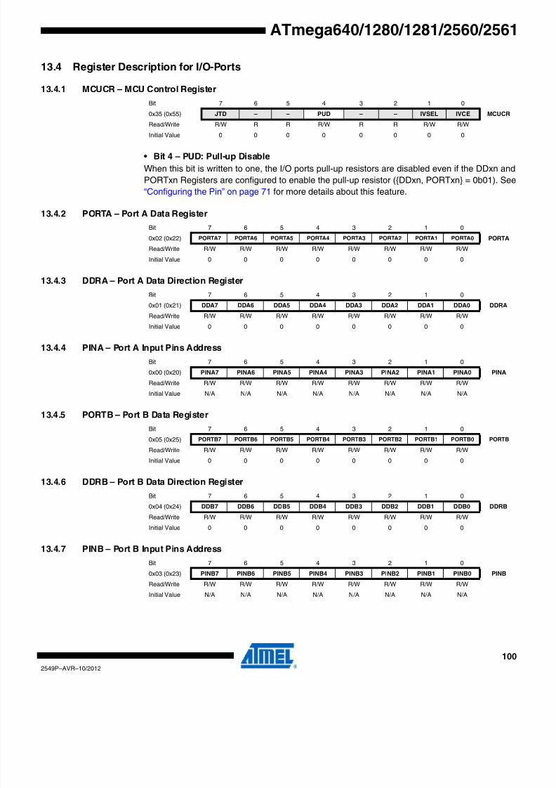
8/20/2019 At Mega 1281 Unlocked
http://slidepdf.com/reader/full/at-mega-1281-unlocked 100/446
100
2549P–AVR–10/2012
ATmega640/1280/1281/2560/2561
13.4 Register Description for I/O-Ports
13.4.1 MCUCR – MCU Control Register
• Bit 4 – PUD: Pull-up Disable
When this bit is written to one, the I/O ports pull-up resistors are disabled even if the DDxn and
PORTxn Registers are configured to enable the pull-up resistor ({DDxn, PORTxn} = 0b01). See
“Configuring the Pin” on page 71 for more details about this feature.
13.4.2 PORTA – Port A Data Register
13.4.3 DDRA – Port A Data Direction Register
13.4.4 PINA – Port A Input Pins Address
13.4.5 PORTB – Port B Data Register
13.4.6 DDRB – Port B Data Direction Register
13.4.7 PINB – Port B Input Pins Address
Bit 7 6 5 4 3 2 1 0
0x35 (0x55) JTD – – PUD – – IVSEL IVCE MCUCR
Read/ Write R/ W R R R/ W R R R/ W R/ W
Initial Value 0 0 0 0 0 0 0 0
Bit 7 6 5 4 3 2 1 0
0x02 (0x22) PORTA7 PORTA6 PORTA5 PORTA4 PORTA3 PORTA2 PORTA1 PORTA0 PORTA
Read/ Write R/ W R/ W R/ W R/ W R/ W R/ W R/ W R/ W
Initial Value 0 0 0 0 0 0 0 0
Bit 7 6 5 4 3 2 1 0
0x01 (0x21) DDA7 DDA6 DDA5 DDA4 DDA3 DDA2 DDA1 DDA0 DDRA
Read/ Write R/ W R/ W R/ W R/ W R/ W R/ W R/ W R/ W
Initial Value 0 0 0 0 0 0 0 0
Bit 7 6 5 4 3 2 1 0
0x00 (0x20) PINA7 PINA6 PINA5 PINA4 PINA3 PINA2 PINA1 PINA0 PINA
Read/ Write R/ W R/ W R/ W R/ W R/ W R/ W R/ W R/ W
Initial Value N /A N /A N /A N /A N /A N /A N /A N /A
Bit 7 6 5 4 3 2 1 0
0x05 (0x25) PORTB7 PORTB6 PORTB5 PORTB4 PORTB3 PORTB2 PORTB1 PORTB0 PORTB
Read/ Write R/ W R/ W R/ W R/ W R/ W R/ W R/ W R/ W
Initial Value 0 0 0 0 0 0 0 0
Bit 7 6 5 4 3 2 1 0
0x04 (0x24) DDB7 DDB6 DDB5 DDB4 DDB3 DDB2 DDB1 DDB0 DDRB
Read/ Write R/ W R/ W R/ W R/ W R/ W R/ W R/ W R/ W
Initial Value 0 0 0 0 0 0 0 0
Bit 7 6 5 4 3 2 1 0
0x03 (0x23) PINB7 PINB6 PINB5 PINB4 PINB3 PINB2 PINB1 PINB0 PINB
Read/ Write R/ W R/ W R/ W R/ W R/ W R/ W R/ W R/ W
Initial Value N /A N /A N /A N /A N /A N /A N /A N /A

8/20/2019 At Mega 1281 Unlocked
http://slidepdf.com/reader/full/at-mega-1281-unlocked 101/446
101
2549P–AVR–10/2012
ATmega640/1280/1281/2560/2561
13.4.8 PORTC – Port C Data Register
13.4.9 DDRC – Port C Data Direction Register
13.4.10 PINC– Port C Input Pins Address
13.4.11 PORTD – Port D Data Register
13.4.12 DDRD – Port D Data Direction Register
13.4.13 PIND – Port D Input Pins Address
13.4.14 PORTE – Port E Data Register
13.4.15 DDRE – Port E Data Direction Register
Bit 7 6 5 4 3 2 1 0
0x08 (0x28) PORTC7 PORTC6 PORTC5 PORTC4 PORTC3 PORTC2 PORTC1 PORTC0 PORTC
Read/ Write R/ W R/ W R/ W R/ W R/ W R/ W R/ W R/ W
Initial Value 0 0 0 0 0 0 0 0
Bit 7 6 5 4 3 2 1 0
0x07 (0x27) DDC7 DDC6 DDC5 DDC4 DDC3 DDC2 DDC1 DDC0 DDRC
Read/ Write R/ W R/ W R/ W R/ W R/ W R/ W R/ W R/ W
Initial Value 0 0 0 0 0 0 0 0
Bit 7 6 5 4 3 2 1 0
0x06 (0x26) PINC7 PINC6 PINC5 PINC4 PINC3 PINC2 PINC1 PINC0 PINC
Read/ Write R/ W R/ W R/ W R/ W R/ W R/ W R/ W R/ W
Initial Value N /A N /A N /A N /A N /A N /A N /A N /A
Bit 7 6 5 4 3 2 1 0
0x0B (0x2B) PORTD7 PORTD6 PORTD5 PORTD4 PORTD3 PORTD2 PORTD1 PORTD0 PORTD
Read/ Write R/ W R/ W R/ W R/ W R/ W R/ W R/ W R/ W
Initial Value 0 0 0 0 0 0 0 0
Bit 7 6 5 4 3 2 1 0
0x0A (0x2A) DDD7 DDD6 DDD5 DDD4 DDD3 DDD2 DDD1 DDD0 DDRD
Read/ Write R/ W R/ W R/ W R/ W R/ W R/ W R/ W R/ W
Initial Value 0 0 0 0 0 0 0 0
Bit 7 6 5 4 3 2 1 0
0x09 (0x29) PIND7 PIND6 PIND5 PIND4 PIND3 PIND2 PIND1 PIND0 PIND
Read/ Write R/ W R/ W R/ W R/ W R/ W R/ W R/ W R/ W
Initial Value N /A N /A N /A N /A N /A N /A N /A N /A
Bit 7 6 5 4 3 2 1 0
0x0E (0x2E) PORTE7 PORTE6 PORTE5 PORTE4 PORTE3 PORTE2 PORTE1 PORTE0 PORTE
Read/ Write R/ W R/ W R/ W R/ W R/ W R/ W R/ W R/ W
Initial Value 0 0 0 0 0 0 0 0
Bit 7 6 5 4 3 2 1 0
0x0D (0x2D) DDE7 DDE6 DDE5 DDE4 DDE3 DDE2 DDE1 DDE0 DDRE
Read/ Write R/ W R/ W R/ W R/ W R/ W R/ W R/ W R/ W
Initial Value 0 0 0 0 0 0 0 0

8/20/2019 At Mega 1281 Unlocked
http://slidepdf.com/reader/full/at-mega-1281-unlocked 102/446
102
2549P–AVR–10/2012
ATmega640/1280/1281/2560/2561
13.4.16 PINE – Port E Input Pins Address
13.4.17 PORTF – Port F Data Register
13.4.18 DDRF – Port F Data Direction Register
13.4.19 PINF – Port F Input Pins Address
13.4.20 PORTG – Port G Data Register
13.4.21 DDRG – Port G Data Direction Register
13.4.22 PING – Port G Input Pins Address
13.4.23 PORTH – Port H Data Register
Bit 7 6 5 4 3 2 1 0
0x0C (0x2C) PINE7 PINE6 PINE5 PINE4 PINE3 PINE2 PINE1 PINE0 PINE
Read/ Write R/ W R/ W R/ W R/ W R/ W R/ W R/ W R/ W
Initial Value N /A N /A N /A N /A N /A N /A N /A N /A
Bit 7 6 5 4 3 2 1 0
0x11 (0x31) PORTF7 PORTF6 PORTF5 PORTF4 PORTF3 PORTF2 PORTF1 PORTF0 PORTF
Read/ Write R/ W R/ W R/ W R/ W R/ W R/ W R/ W R/ W
Initial Value 0 0 0 0 0 0 0 0
Bit 7 6 5 4 3 2 1 0
0x10 (0x30) DDF7 DDF6 DDF5 DDF4 DDF3 DDF2 DDF1 DDF0 DDRF
Read/ Write R/ W R/ W R/ W R/ W R/ W R/ W R/ W R/ W
Initial Value 0 0 0 0 0 0 0 0
Bit 7 6 5 4 3 2 1 0
0x0F (0x2F) PINF7 PINF6 PINF5 PINF4 PINF3 PINF2 PINF1 PINF0 PINF
Read/ Write R/ W R/ W R/ W R/ W R/ W R/ W R/ W R/ W
Initial Value N /A N /A N /A N /A N /A N /A N /A N /A
Bit 7 6 5 4 3 2 1 0
0x14 (0x34) – – PORTG5 PORTG4 PORTG3 PORTG2 PORTG1 PORTG0 PORTG
Read/ Write R R R/ W R/ W R/ W R/ W R/ W R/ W
Initial Value 0 0 0 0 0 0 0 0
Bit 7 6 5 4 3 2 1 0
0x13 (0x33) – – DDG5 DDG4 DDG3 DDG2 DDG1 DDG0 DDRG
Read/ Write R R R/ W R/ W R/ W R/ W R/ W R/ W
Initial Value 0 0 0 0 0 0 0 0
Bit 7 6 5 4 3 2 1 0
0x12 (0x32) – – PING5 PING4 PING3 PING2 PING1 PING0 PING
Read/ Write R R R/ W R/ W R/ W R/ W R/ W R/ W
Initial Value 0 0 N /A N /A N /A N /A N /A N /A
Bit 7 6 5 4 3 2 1 0
(0x102) PORTH7 PORTH6 PORTH5 PORTH4 PORTH3 PORTH2 PORTH1 PORTH0 PORTH
Read/ Write R/ W R/ W R/ W R/ W R/ W R/ W R/ W R/ W
Initial Value 0 0 0 0 0 0 0 0
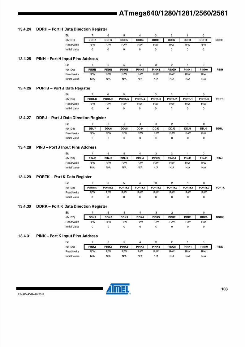
8/20/2019 At Mega 1281 Unlocked
http://slidepdf.com/reader/full/at-mega-1281-unlocked 103/446
103
2549P–AVR–10/2012
ATmega640/1280/1281/2560/2561
13.4.24 DDRH – Port H Data Direction Register
13.4.25 PINH – Port H Input Pins Address
13.4.26 PORTJ – Port J Data Register
13.4.27 DDRJ – Port J Data Direction Register
13.4.28 PINJ – Port J Input Pins Address
13.4.29 PORTK – Port K Data Register
13.4.30 DDRK – Port K Data Direction Register
13.4.31 PINK – Port K Input Pins Address
Bit 7 6 5 4 3 2 1 0
(0x101) DDH7 DDH6 DDH5 DDH4 DDH3 DDH2 DDH1 DDH0 DDRH
Read/ Write R/ W R/ W R/ W R/ W R/ W R/ W R/ W R/ W
Initial Value 0 0 0 0 0 0 0 0
Bit 7 6 5 4 3 2 1 0
(0x100) PINH5 PINH5 PINH5 PINH4 PINH3 PINGH PINH1 PINH0 PINH
Read/ Write R/ W R/ W R/ W R/ W R/ W R/ W R/ W R/ W
Initial Value N /A N /A N /A N /A N /A N /A N /A N /A
Bit 7 6 5 4 3 2 1 0
(0x105) PORTJ7 PORTJ6 PORTJ5 PORTJ4 PORTJ3 PORTJ2 PORTJ1 PORTJ0 PORTJ
Read/ Write R/ W R/ W R/ W R/ W R/ W R/ W R/ W R/ W
Initial Value 0 0 0 0 0 0 0 0
Bit 7 6 5 4 3 2 1 0
(0x104) DDJ7 DDJ6 DDJ5 DDJ4 DDJ3 DDJ2 DDJ1 DDJ0 DDRJ
Read/ Write R/ W R/ W R/ W R/ W R/ W R/ W R/ W R/ W
Initial Value 0 0 0 0 0 0 0 0
Bit 7 6 5 4 3 2 1 0
(0x103) PINJ5 PINJ5 PINJ5 PINJ4 PINJ3 PINGJ PINJ1 PINJ0 PINJ
Read/ Write R/ W R/ W R/ W R/ W R/ W R/ W R/ W R/ W
Initial Value N /A N /A N /A N /A N /A N /A N /A N /A
Bit 7 6 5 4 3 2 1 0
(0x108) PORTK7 PORTK6 PORTK5 PORTK4 PORTK3 PORTK2 PORTK1 PORTK0 PORTK
Read/ Write R/ W R/ W R/ W R/ W R/ W R/ W R/ W R/ W
Initial Value 0 0 0 0 0 0 0 0
Bit 7 6 5 4 3 2 1 0
(0x107) DDK7 DDK6 DDK5 DDK4 DDK3 DDK2 DDK1 DDK0 DDRK
Read/ Write R/ W R/ W R/ W R/ W R/ W R/ W R/ W R/ W
Initial Value 0 0 0 0 0 0 0 0
Bit 7 6 5 4 3 2 1 0
(0x106) PINK5 PINK5 PINK5 PINK4 PINK3 PINGK PINK1 PINK0 PINK
Read/ Write R/ W R/ W R/ W R/ W R/ W R/ W R/ W R/ W
Initial Value N /A N /A N /A N /A N /A N /A N /A N /A

8/20/2019 At Mega 1281 Unlocked
http://slidepdf.com/reader/full/at-mega-1281-unlocked 104/446
104
2549P–AVR–10/2012
ATmega640/1280/1281/2560/2561
13.4.32 PORTL – Port L Data Register
13.4.33 DDRL – Port L Data Direction Register
13.4.34 PINL – Port L Input Pins Address
Bit 7 6 5 4 3 2 1 0
(0x10B) PORTL7 PORTL6 PORTL5 PORTL4 PORTL3 PORTL2 PORTL1 PORTL0 PORTL
Read/ Write R/ W R/ W R/ W R/ W R/ W R/ W R/ W R/ W
Initial Value 0 0 0 0 0 0 0 0
Bit 7 6 5 4 3 2 1 0
(0x10A) DDL7 DDL6 DDL5 DDL4 DDL3 DDL2 DDL1 DDL0 DDRL
Read/ Write R/ W R/ W R/ W R/ W R/ W R/ W R/ W R/ W
Initial Value 0 0 0 0 0 0 0 0
Bit 7 6 5 4 3 2 1 0
(0x109) PINL5 PINL5 PINL5 PINL4 PINL3 PINGL PINL1 PINL0 PINL
Read/ Write R/ W R/ W R/ W R/ W R/ W R/ W R/ W R/ W
Initial Value N /A N /A N /A N /A N /A N /A N /A N /A

8/20/2019 At Mega 1281 Unlocked
http://slidepdf.com/reader/full/at-mega-1281-unlocked 105/446
105
2549P–AVR–10/2012
ATmega640/1280/1281/2560/2561
14. InterruptsThis sect ion descr ibes the speci f ics of the in ter rupt handl ing as per formed in
ATmega640/1280/1281/2560/2561. For a general explanation of the AVR interrupt handling
refer to “Reset and Interrupt Handling” on page 18.
14.1 Interrupt Vectors in ATmega640/1280/1281/2560/2561Table 14-1. Reset and Interrupt Vectors
Vector
No.
Program
Address(2) Source Interrupt Definition
1 $0000(1) RESETExternal Pin, Power-on Reset, Brown-out Reset,
Watchdog Reset, and JTAG AVR Reset
2 $0002 INT0 External Interrupt Request 0
3 $0004 INT1 External Interrupt Request 1
4 $0006 INT2 External Interrupt Request 2
5 $0008 INT3 External Interrupt Request 3
6 $000A INT4 External Interrupt Request 4
7 $000C INT5 External Interrupt Request 5
8 $000E INT6 External Interrupt Request 6
9 $0010 INT7 External Interrupt Request 7
10 $0012 PCINT0 Pin Change Interrupt Request 0
11 $0014 PCINT1 Pin Change Interrupt Request 1
12 $0016(3) PCINT2 Pin Change Interrupt Request 2
13 $0018 WDT Watchdog Time-out Interrupt
14 $001A TIMER2 COMPA Timer/Counter2 Compare Match A
15 $001C TIMER2 COMPB Timer/Counter2 Compare Match B
16 $001E TIMER2 OVF Timer/Counter2 Overflow
17 $0020 TIMER1 CAPT Timer/Counter1 Capture Event
18 $0022 TIMER1 COMPA Timer/Counter1 Compare Match A
19 $0024 TIMER1 COMPB Timer/Counter1 Compare Match B
20 $0026 TIMER1 COMPC Timer/Counter1 Compare Match C
21 $0028 TIMER1 OVF Timer/Counter1 Overflow
22 $002A TIMER0 COMPA Timer/Counter0 Compare Match A
23 $002C TIMER0 COMPB Timer/Counter0 Compare match B
24 $002E TIMER0 OVF Timer/Counter0 Overflow
25 $0030 SPI, STC SPI Serial Transfer Complete
26 $0032 USART0 RX USART0 Rx Complete
27 $0034 USART0 UDRE USART0 Data Register Empty
28 $0036 USART0 TX USART0 Tx Complete
29 $0038 ANALOG COMP Analog Comparator

8/20/2019 At Mega 1281 Unlocked
http://slidepdf.com/reader/full/at-mega-1281-unlocked 106/446
106
2549P–AVR–10/2012
ATmega640/1280/1281/2560/2561
Notes: 1. When the BOOTRST Fuse is programmed, the device will jump to the Boot Loader address at
reset, see “Memory Programming” on page 335.2. When the IVSEL bit in MCUCR is set, Interrupt Vectors will be moved to the start of the Boot
Flash Section. The address of each Interrupt Vector will then be the address in this tableadded to the start address of the Boot Flash Section.
3. Only available in ATmega640/1280/2560.
30 $003A ADC ADC Conversion Complete
31 $003C EE READY EEPROM Ready
32 $003E TIMER3 CAPT Timer/Counter3 Capture Event
33 $0040 TIMER3 COMPA Timer/Counter3 Compare Match A
34 $0042 TIMER3 COMPB Timer/Counter3 Compare Match B
35 $0044 TIMER3 COMPC Timer/Counter3 Compare Match C
36 $0046 TIMER3 OVF Timer/Counter3 Overflow
37 $0048 USART1 RX USART1 Rx Complete
38 $004A USART1 UDRE USART1 Data Register Empty
39 $004C USART1 TX USART1 Tx Complete
40 $004E TWI 2-wire Serial Interface
41 $0050 SPM READY Store Program Memory Ready
42 $0052(3) TIMER4 CAPT Timer/Counter4 Capture Event
43 $0054 TIMER4 COMPA Timer/Counter4 Compare Match A
44 $0056 TIMER4 COMPB Timer/Counter4 Compare Match B
45 $0058 TIMER4 COMPC Timer/Counter4 Compare Match C
46 $005A TIMER4 OVF Timer/Counter4 Overflow
47 $005C(3) TIMER5 CAPT Timer/Counter5 Capture Event
48 $005E TIMER5 COMPA Timer/Counter5 Compare Match A
49 $0060 TIMER5 COMPB Timer/Counter5 Compare Match B
50 $0062 TIMER5 COMPC Timer/Counter5 Compare Match C
51 $0064 TIMER5 OVF Timer/Counter5 Overflow
52 $0066(3) USART2 RX USART2 Rx Complete
53 $0068(3) USART2 UDRE USART2 Data Register Empty
54 $006A(3) USART2 TX USART2 Tx Complete
55 $006C(3) USART3 RX USART3 Rx Complete
56 $006E(3)) USART3 UDRE USART3 Data Register Empty
57 $0070(3) USART3 TX USART3 Tx Complete
Table 14-1. Reset and Interrupt Vectors (Continued)
Vector
No.
Program
Address(2) Source Interrupt Definition

8/20/2019 At Mega 1281 Unlocked
http://slidepdf.com/reader/full/at-mega-1281-unlocked 107/446
107
2549P–AVR–10/2012
ATmega640/1280/1281/2560/2561
14.2 Reset and Interrupt Vector placement
Table 14-2 shows Reset and Interrupt Vectors placement for the various combinations of
BOOTRST and IVSEL settings. If the program never enables an interrupt source, the Interrup
Vectors are not used, and regular program code can be placed at these locations. This is also
the case if the Reset Vector is in the Application section while the Interrupt Vectors are in the
Boot section or vice versa.
Note: 1. The Boot Reset Address is shown in Table 29-7 on page 328 through Table 29-15 on page332. For the BOOTRST Fuse “1” means unprogrammed while “0” means programmed.
The most typical and general program setup for the Reset and Interrupt Vector Addresses in
ATmega640/1280/1281/2560/2561 is:
Table 14-2. Reset and Interrupt Vectors Placement(1)
BOOTRST IVSEL Reset Address Interrupt Vectors Start Address
1 0 0x0000 0x0002
1 1 0x0000 Boot Reset Address + 0x0002
0 0 Boot Reset Address 0x0002
0 1 Boot Reset Address Boot Reset Address + 0x0002
Address Labels Code Comments
0x0000 jmp RESET ; Reset Handler
0x0002 jmp INT0 ; IRQ0 Handler
0x0004 jmp INT1 ; IRQ1 Handler
0x0006 jmp INT2 ; IRQ2 Handler
0x0008 jmp INT3 ; IRQ3 Handler
0x000A jmp INT4 ; IRQ4 Handler
0x000C jmp INT5 ; IRQ5 Handler
0x000E jmp INT6 ; IRQ6 Handler
0x0010 jmp INT7 ; IRQ7 Handler
0x0012 jmp PCINT0 ; PCINT0 Handler
0x0014 jmp PCINT1 ; PCINT1 Handler
0x0016 jmp PCINT2 ; PCINT2 Handler
0X0018 jmp WDT ; Watchdog Timeout Handler
0x001A jmp TIM2_COMPA ; Timer2 CompareA Handler
0x001C jmp TIM2_COMPB ; Timer2 CompareB Handler
0x001E jmp TIM2_OVF ; Timer2 Overflow Handler
0x0020 jmp TIM1_CAPT ; Timer1 Capture Handler
0x0022 jmp TIM1_COMPA ; Timer1 CompareA Handler
0x0024 jmp TIM1_COMPB ; Timer1 CompareB Handler
0x0026 jmp TIM1_COMPC ; Timer1 CompareC Handler
0x0028 jmp TIM1_OVF ; Timer1 Overflow Handler
0x002A jmp TIM0_COMPA ; Timer0 CompareA Handler
0x002C jmp TIM0_COMPB ; Timer0 CompareB Handler
0x002E jmp TIM0_OVF ; Timer0 Overflow Handler
0x0030 jmp SPI_STC ; SPI Transfer Complete Handler
0x0032 jmp USART0_RXC ; USART0 RX Complete Handler
0x0034 jmp USART0_UDRE ; USART0,UDR Empty Handler
0x0036 jmp USART0_TXC ; USART0 TX Complete Handler
0x0038 jmp ANA_COMP ; Analog Comparator Handler
0x003A jmp ADC ; ADC Conversion Complete Handler
0x003C jmp EE_RDY ; EEPROM Ready Handler
0x003E jmp TIM3_CAPT ; Timer3 Capture Handler

8/20/2019 At Mega 1281 Unlocked
http://slidepdf.com/reader/full/at-mega-1281-unlocked 108/446
108
2549P–AVR–10/2012
ATmega640/1280/1281/2560/2561
When the BOOTRST Fuse is unprogrammed, the Boot section size set to 8Kbytes and the
IVSEL bit in the MCUCR Register is set before any interrupts are enabled, the most typical and
general program setup for the Reset and Interrupt Vector Addresses is:
Address Labels Code Comments
0x00000 RESET: ldi r16,high(RAMEND); Main program start
0x00001 out SPH,r16 ; Set Stack Pointer to top of RAM
0x00002 ldi r16,low(RAMEND)
0x00003 out SPL,r160x00004 sei ; Enable interrupts
0x00005 <instr> xxx
;
.org 0x1F002
0x1F002 jmp EXT_INT0 ; IRQ0 Handler
0x1F004 jmp EXT_INT1 ; IRQ1 Handler
... ... ... ;
0x1FO70 jmp USART3_TXC ; USART3 TX Complete Handler
0x0040 jmp TIM3_COMPA ; Timer3 CompareA Handler
0x0042 jmp TIM3_COMPB ; Timer3 CompareB Handler
0x0044 jmp TIM3_COMPC ; Timer3 CompareC Handler
0x0046 jmp TIM3_OVF ; Timer3 Overflow Handler
0x0048 jmp USART1_RXC ; USART1 RX Complete Handler
0x004A jmp USART1_UDRE ; USART1,UDR Empty Handler
0x004C jmp USART1_TXC ; USART1 TX Complete Handler0x004E jmp TWI ; 2-wire Serial Handler
0x0050 jmp SPM_RDY ; SPM Ready Handler
0x0052 jmp TIM4_CAPT ; Timer4 Capture Handler
0x0054 jmp TIM4_COMPA ; Timer4 CompareA Handler
0x0056 jmp TIM4_COMPB ; Timer4 CompareB Handler
0x0058 jmp TIM4_COMPC ; Timer4 CompareC Handler
0x005A jmp TIM4_OVF ; Timer4 Overflow Handler
0x005C jmp TIM5_CAPT ; Timer5 Capture Handler
0x005E jmp TIM5_COMPA ; Timer5 CompareA Handler
0x0060 jmp TIM5_COMPB ; Timer5 CompareB Handler
0x0062 jmp TIM5_COMPC ; Timer5 CompareC Handler
0x0064 jmp TIM5_OVF ; Timer5 Overflow Handler
0x0066 jmp USART2_RXC ; USART2 RX Complete Handler0x0068 jmp USART2_UDRE ; USART2,UDR Empty Handler
0x006A jmp USART2_TXC ; USART2 TX Complete Handler
0x006C jmp USART3_RXC ; USART3 RX Complete Handler
0x006E jmp USART3_UDRE ; USART3,UDR Empty Handler
0x0070 jmp USART3_TXC ; USART3 TX Complete Handler
;
0x0072 RESET: ldi r16, high(RAMEND) ; Main program start
0x0073 out SPH,r16 ; Set Stack Pointer to top of RAM
0x0074 ldi r16, low(RAMEND)
0x0075 out SPL,r16
0x0076 sei ; Enable interrupts
0x0077 <instr> xxx
... ... ... ...

8/20/2019 At Mega 1281 Unlocked
http://slidepdf.com/reader/full/at-mega-1281-unlocked 109/446
109
2549P–AVR–10/2012
ATmega640/1280/1281/2560/2561
When the BOOTRST Fuse is programmed and the Boot section size set to 8Kbytes, the most
typical and general program setup for the Reset and Interrupt Vector Addresses is:
Address Labels Code Comments
.org 0x0002
0x00002 jmp EXT_INT0 ; IRQ0 Handler
0x00004 jmp EXT_INT1 ; IRQ1 Handler
... ... ... ;
0x00070 jmp USART3_TXC ; USART3 TX Complete Handler
;
.org 0x1F0000x1F000 RESET: ldi r16,high(RAMEND); Main program start
0x1F001 out SPH,r16 ; Set Stack Pointer to top of RAM
0x1F002 ldi r16,low(RAMEND)
0x1F003 out SPL,r160x1F004 sei ; Enable interrupts
0x1F005 <instr> xxx
When the BOOTRST Fuse is programmed, the Boot section size set to 8Kbytes and the IVSELbit in the MCUCR Register is set before any interrupts are enabled, the most typical and genera
program setup for the Reset and Interrupt Vector Addresses is:
Address Labels Code Comments
;
.org 0x1F000
0x1F000 jmp RESET ; Reset handler
0x1F002 jmp EXT_INT0 ; IRQ0 Handler
0x1F004 jmp EXT_INT1 ; IRQ1 Handler
... ... ... ;
0x1F070 jmp USART3_TXC ; USART3 TX Complete Handler
;
0x1F072 RESET: ldi r16,high(RAMEND) ; Main program start
0x1F073 out SPH,r16 ; Set Stack Pointer to top of RAM
0x1F074 ldi r16,low(RAMEND)
0x1F075 out SPL,r160x1F076 sei ; Enable interrupts
0x1FO77 <instr> xxx
14.3 Moving Interrupts Between Application and Boot Section
The MCU Control Register controls the placement of the Interrupt Vector table, see Code Exam-
ple below. For more details, see “Reset and Interrupt Handling” on page 18.

8/20/2019 At Mega 1281 Unlocked
http://slidepdf.com/reader/full/at-mega-1281-unlocked 110/446
110
2549P–AVR–10/2012
ATmega640/1280/1281/2560/2561
14.4 Register Description
14.4.1 MCUCR – MCU Control Register
• Bit 1 – IVSEL: Interrupt Vector Select
When the IVSEL bit is cleared (zero), the Interrupt Vectors are placed at the start of the Flash
memory. When this bit is set (one), the Interrupt Vectors are moved to the beginning of the BooLoader section of the Flash. The actual address of the start of the Boot Flash Section is deter-
mined by the BOOTSZ Fuses. Refer to the section “Memory Programming” on page 335 for
details. To avoid unintentional changes of Interrupt Vector tables, a special write procedure mus
be followed to change the IVSEL bit (see “Moving Interrupts Between Application and Boot Sec-
tion” on page 109):
1. Write the Interrupt Vector Change Enable (IVCE) bit to one.
2. Within four cycles, write the desired value to IVSEL while writing a zero to IVCE.
Assembly Code Example
Move_interrupts:
; Get MCUCR
in r16, MCUCR
mov r17, r16
; Enable change of Interrupt Vectors
ori r16, (1<<IVCE)
out MCUCR, r16
; Move interrupts to Boot Flash section
ori r16, (1<<IVSEL)
out MCUCR, r17
ret
C Code Example
void Move_interrupts( void)
{
uchar temp;
/* Get MCUCR*/
temp = MCUCR;
/* Enable change of Interrupt Vectors */
MCUCR = temp|(1<<IVCE);
/* Move interrupts to Boot Flash section */
MCUCR = temp|(1<<IVSEL);
}
Bit 7 6 5 4 3 2 1 0
0x35 (0x55) JTD – – PUD – – IVSEL IVCE MCUCR
Read/ Write R/ W R R R/ W R R R/ W R/ W
Initial Value 0 0 0 0 0 0 0 0

8/20/2019 At Mega 1281 Unlocked
http://slidepdf.com/reader/full/at-mega-1281-unlocked 111/446
111
2549P–AVR–10/2012
ATmega640/1280/1281/2560/2561
Interrupts will automatically be disabled while this sequence is executed. Interrupts are disabled
in the cycle IVCE is set, and they remain disabled until after the instruction following the write to
IVSEL. If IVSEL is not written, interrupts remain disabled for four cycles. The I-bit in the Status
Register is unaffected by the automatic disabling.
Note: If Interrupt Vectors are placed in the Boot Loader section and Boot Lock bit BLB02 is programmed,interrupts are disabled while executing from the Application section. If Interrupt Vectors are placed
in the Application section and Boot Lock bit BLB12 is programed, interrupts are disabled whileexecuting from the Boot Loader section. Refer to the section “Memory Programming” on page 335for details on Boot Lock bits.
• Bit 0 – IVCE: Interrupt Vector Change Enable
The IVCE bit must be written to logic one to enable change of the IVSEL bit. IVCE is cleared by
hardware four cycles after it is written or when IVSEL is written. Setting the IVCE bit will disable
interrupts, as explained in the IVSEL description.
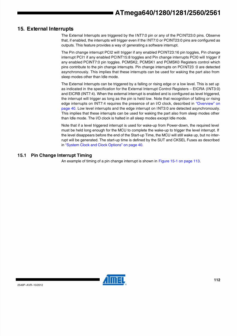
8/20/2019 At Mega 1281 Unlocked
http://slidepdf.com/reader/full/at-mega-1281-unlocked 112/446
112
2549P–AVR–10/2012
ATmega640/1280/1281/2560/2561
15. External InterruptsThe External Interrupts are triggered by the INT7:0 pin or any of the PCINT23:0 pins. Observe
that, if enabled, the interrupts will trigger even if the INT7:0 or PCINT23:0 pins are configured as
outputs. This feature provides a way of generating a software interrupt.
The Pin change interrupt PCI2 will trigger if any enabled PCINT23:16 pin toggles, Pin change
interrupt PCI1 if any enabled PCINT15:8 toggles and Pin change interrupts PCI0 will trigger iany enabled PCINT7:0 pin toggles. PCMSK2, PCMSK1 and PCMSK0 Registers control which
pins contribute to the pin change interrupts. Pin change interrupts on PCINT23 :0 are detected
asynchronously. This implies that these interrupts can be used for waking the part also from
sleep modes other than Idle mode.
The External Interrupts can be triggered by a falling or rising edge or a low level. This is set up
as indicated in the specification for the External Interrupt Control Registers – EICRA (INT3:0
and EICRB (INT7:4). When the external interrupt is enabled and is configured as level triggered
the interrupt will trigger as long as the pin is held low. Note that recognition of falling or rising
edge interrupts on INT7:4 requires the presence of an I/O clock, described in “Overview” on
page 40. Low level interrupts and the edge interrupt on INT3:0 are detected asynchronously
This implies that these interrupts can be used for waking the part also from sleep modes otherthan Idle mode. The I/O clock is halted in all sleep modes except Idle mode.
Note that if a level triggered interrupt is used for wake-up from Power-down, the required level
must be held long enough for the MCU to complete the wake-up to trigger the level interrupt. If
the level disappears before the end of the Start-up Time, the MCU will still wake up, but no inter-
rupt will be generated. The start-up time is defined by the SUT and CKSEL Fuses as described
in “System Clock and Clock Options” on page 40.
15.1 Pin Change Interrupt Timing
An example of timing of a pin change interrupt is shown in Figure 15-1 on page 113.

8/20/2019 At Mega 1281 Unlocked
http://slidepdf.com/reader/full/at-mega-1281-unlocked 113/446
113
2549P–AVR–10/2012
ATmega640/1280/1281/2560/2561
Figure 15-1. Normal pin change interrupt.
15.2 Register Description
15.2.1 EICRA – External Interrupt Control Register A
The External Interrupt Control Register A contains control bits for interrupt sense control.
• Bits 7:0 – ISC31, ISC30 – ISC00, ISC00: External Interrupt 3 - 0 Sense Control Bits
The External Interrupts 3 - 0 are activated by the external pins INT3:0 if the SREG I-flag and the
corresponding interrupt mask in the EIMSK is set. The level and edges on the external pins tha
activate the interrupts are defined in Table 15-1 on page 114. Edges on INT3:0 are registered
asynchronously. Pulses on INT3:0 pins wider than the minimum pulse width given in Table 15-2
on page 114 will generate an interrupt. Shorter pulses are not guaranteed to generate an inter-
rupt. If low level interrupt is selected, the low level must be held until the completion of the
currently executing instruction to generate an interrupt. If enabled, a level triggered interrupt wil
generate an interrupt request as long as the pin is held low. When changing the ISCn bit, aninterrupt can occur. Therefore, it is recommended to first disable INTn by clearing its Interrup
Enable bit in the EIMSK Register. Then, the ISCn bit can be changed. Finally, the INTn interrup
flag should be cleared by writing a logical one to its Interrupt Flag bit (INTFn) in the EIFR Regis
ter before the interrupt is re-enabled.
clk
PCINT(n)
pin_lat
pin_sync
pcint_in_(n)
pcint_syn
pcint_setflag
PCIF
PCINT(0)
pin_sync
pcint_synpin_lat
D Q
LE
pcint_setflagPCIF
clkclkPCINT(0) in PCMSK(x)
pcint_in_(0)0
x
Bit 7 6 5 4 3 2 1 0
(0x69) ISC31 ISC30 ISC21 ISC20 ISC11 ISC10 ISC01 ISC00 EICRA
Read/ Write R/ W R/ W R/ W R/ W R/ W R/ W R/ W R/ W
Initial Value 0 0 0 0 0 0 0 0

8/20/2019 At Mega 1281 Unlocked
http://slidepdf.com/reader/full/at-mega-1281-unlocked 114/446
114
2549P–AVR–10/2012
ATmega640/1280/1281/2560/2561
Note: 1. n = 3, 2, 1or 0.When changing the ISCn1/ISCn0 bits, the interrupt must be disabled by clearing its InterruptEnable bit in the EIMSK Register. Otherwise an interrupt can occur when the bits are changed
15.2.2 EICRB – External Interrupt Control Register B
• Bits 7:0 – ISC71, ISC70 - ISC41, ISC40: External Interrupt 7 - 4 Sense Control Bits
The External Interrupts 7 - 4 are activated by the external pins INT7:4 if the SREG I-flag and the
corresponding interrupt mask in the EIMSK is set. The level and edges on the external pins tha
activate the interrupts are defined in Table 15-3. The value on the IN
T7:4 pins are sampledbefore detecting edges. If edge or toggle interrupt is selected, pulses that last longer than one
clock period will generate an interrupt. Shorter pulses are not guaranteed to generate an inter-
rupt. Observe that CPU clock frequency can be lower than the XTAL frequency if the XTAL
divider is enabled. If low level interrupt is selected, the low level must be held until the comple-
tion of the currently executing instruction to generate an interrupt. If enabled, a level triggered
interrupt will generate an interrupt request as long as the pin is held low.
Note: 1. n = 7, 6, 5 or 4.When changing the ISCn1/ISCn0 bits, the interrupt must be disabled by clearing its InterruptEnable bit in the EIMSK Register. Otherwise an interrupt can occur when the bits are changed
Table 15-1. Interrupt Sense Control(1)
ISCn1 ISCn0 Description
0 0 The low level of INTn generates an interrupt request
0 1 Any edge of IN
Tn generates asynchronously an interrupt request1 0 The falling edge of INTn generates asynchronously an interrupt request
1 1 The rising edge of INTn generates asynchronously an interrupt request
Table 15-2. Asynchronous External Interrupt Characteristics
Symbol Parameter Condition Min Typ Max Units
tINT
Minimum pulse width for asynchronous
external interrupt 50 ns
Bit 7 6 5 4 3 2 1 0
(0x6A) ISC71 ISC70 ISC61 ISC60 ISC51 ISC50 ISC41 ISC40 EICRB
Read/ Write R/ W R/ W R/ W R/ W R/ W R/ W R/ W R/ W
Initial Value 0 0 0 0 0 0 0 0
Table 15-3. Interrupt Sense Control(1)
ISCn1 ISCn0 Description
0 0 The low level of INTn generates an interrupt request
0 1 Any logical change on INTn generates an interrupt request
1 0 The falling edge between two samples of INTn generates an interrupt request
1 1 The rising edge between two samples of INTn generates an interrupt request

8/20/2019 At Mega 1281 Unlocked
http://slidepdf.com/reader/full/at-mega-1281-unlocked 115/446
115
2549P–AVR–10/2012
ATmega640/1280/1281/2560/2561
15.2.3 EIMSK – External Interrupt Mask Register
• Bits 7:0 – INT7:0: External Interrupt Request 7 - 0 Enable
When an INT7:0 bit is written to one and the I-bit in the Status Register (SREG) is set (one), the
corresponding external pin interrupt is enabled. The Interrupt Sense Control bits in the Externa
Interrupt Control Registers – EICRA and EICRB – defines whether the external interrupt is acti-
vated on rising or falling edge or level sensed. Activity on any of these pins will trigger an
interrupt request even if the pin is enabled as an output. This provides a way of generating a
software interrupt.
15.2.4 EIFR – External Interrupt Flag Register
• Bits 7:0 – INTF7:0: External Interrupt Flags 7 - 0
When an edge or logic change on the INT7:0 pin triggers an interrupt request, INTF7:0 becomes
set (one). If the I-bit in SREG and the corresponding interrupt enable bit, I NT7:0 in EIMSK, are
set (one), the MCU will jump to the interrupt vector. The flag is cleared when the interrupt routine
is executed. Alternatively, the flag can be cleared by writing a logical one to it. These flags are
always cleared when INT7:0 are configured as level interrupt. Note that when entering sleep
mode with the INT3:0 interrupts disabled, the input buffers on these pins will be disabled. This
may cause a logic change in internal signals which will set the INTF3:0 flags. See “Digital Inpu
Enable and Sleep Modes” on page 74 for more information.
15.2.5 PCICR – Pin Change Interrupt Control Register
• Bit 2 – PCIE2: Pin Change Interrupt Enable 1
When the PCIE2 bit is set (one) and the I-bit in the Status Register (SREG) is set (one), pin
change interrupt 2 is enabled. Any change on any enabled PCINT23:16 pin will cause an inter
rupt. The corresponding interrupt of Pin Change Interrupt Request is executed from the PCI2
Interrupt Vector. PCINT23:16 pins are enabled individually by the PCMSK2 Register.
• Bit 1 – PCIE1: Pin Change Interrupt Enable 1
When the PCIE1 bit is set (one) and the I-bit in the Status Register (SREG) is set (one), pin
change interrupt 1 is enabled. Any change on any enabled PCINT15:8 pin will cause an inter
rupt. The corresponding interrupt of Pin Change Interrupt Request is executed from the PCI1
Interrupt Vector. PCINT15:8 pins are enabled individually by the PCMSK1 Register.
Bit 7 6 5 4 3 2 1 0
0x1D (0x3D) INT7 INT6 INT5 INT4 INT3 INT2 INT1 INT0 EIMSK
Read/ Write R/ W R/ W R/ W R/ W R/ W R/ W R/ W R/ W
Initial Value 0 0 0 0 0 0 0 0
Bit 7 6 5 4 3 2 1 0
0x1C (0x3C) INTF7 INTF6 INTF5 INTF4 INTF3 INTF2 INTF1 IINTF0 EIFR
Read/ Write R/ W R/ W R/ W R/ W R/ W R/ W R/ W R/ W
Initial Value 0 0 0 0 0 0 0 0
Bit 7 6 5 4 3 2 1 0
(0x68) – – – – – PCIE2 PCIE1 PCIE0 PCICR
Read/ Write R R R R R R/ W R/ W R/ W
Initial Value 0 0 0 0 0 0 0 0

8/20/2019 At Mega 1281 Unlocked
http://slidepdf.com/reader/full/at-mega-1281-unlocked 116/446
116
2549P–AVR–10/2012
ATmega640/1280/1281/2560/2561
• Bit 0 – PCIE0: Pin Change Interrupt Enable 0
When the PCIE0 bit is set (one) and the I-bit in the Status Register (SREG) is set (one), pin
change interrupt 0 is enabled. Any change on any enabled PCINT7:0 pin will cause an interrupt
The corresponding interrupt of Pin Change Interrupt Request is executed from the PCI0 Interrup
Vector. PCINT7:0 pins are enabled individually by the PCMSK0 Register.
15.2.6 PCIFR – Pin Change Interrupt Flag Register
• Bit 2 – PCIF2: Pin Change Interrupt Flag 1
When a logic change on any PCINT23:16 pin triggers an interrupt request, PCIF2 becomes set
(one). If the I-bit in SREG and the PCIE2 bit in PCICR are set (one), the MCU will jump to the
corresponding Interrupt Vector. The flag is cleared when the interrupt routine is executed. Alter-
natively, the flag can be cleared by writing a logical one to it.
• Bit 1 – PCIF1: Pin Change Interrupt Flag 1When a logic change on any PCINT15:8 pin triggers an interrupt request, PCIF1 becomes se
(one). If the I-bit in SREG and the PCIE1 bit in PCICR are set (one), the MCU will jump to the
corresponding Interrupt Vector. The flag is cleared when the interrupt routine is executed. Alter-
natively, the flag can be cleared by writing a logical one to it.
• Bit 0 – PCIF0: Pin Change Interrupt Flag 0
When a logic change on any PCINT7:0 pin triggers an interrupt request, PCIF0 becomes se
(one). If the I-bit in SREG and the PCIE0 bit in PCICR are set (one), the MCU will jump to the
corresponding Interrupt Vector. The flag is cleared when the interrupt routine is executed. Alter-
natively, the flag can be cleared by writing a logical one to it.
15.2.7 PCMSK2 – Pin Change Mask Register 2
• Bit 7:0 – PCINT23:16: Pin Change Enable Mask 23:16
Each PCINT23:16-bit selects whether pin change interrupt is enabled on the corresponding I/O
pin. If PCINT23:16 is set and the PCIE2 bit in PCICR is set, pin change interrupt is enabled on
the corresponding I/O pin. If PCINT23:16 is cleared, pin change interrupt on the corresponding
I/O pin is disabled.
15.2.8 PCMSK1 – Pin Change Mask Register 1
Bit 7 6 5 4 3 2 1 0
0x1B (0x3B) – – – – – PCIF2 PCIF1 PCIF0 PCIFR
Read/ Write R R R R R R/ W R/ W R/ W
Initial Value 0 0 0 0 0 0 0 0
Bit 7 6 5 4 3 2 1 0
(0x6D) PCINT23 PCINT22 PCINT21 PCINT20 PCINT19 PCINT18 PCINT17 PCINT16 PCMSK2
Read/ Write R/ W R/ W R/ W R/ W R/ W R/ W R/ W R/ W
Initial Value 0 0 0 0 0 0 0 0
Bit 7 6 5 4 3 2 1 0
(0x6C) PCINT15 PCINT14 PCINT13 PCINT12 PCINT11 PCINT10 PCINT9 PCINT8 PCMSK1
Read/ Write R/ W R/ W R/ W R/ W R/ W R/ W R/ W R/ W
Initial Value 0 0 0 0 0 0 0 0
8/20/2019 At Mega 1281 Unlocked
http://slidepdf.com/reader/full/at-mega-1281-unlocked 117/446
117
2549P–AVR–10/2012
ATmega640/1280/1281/2560/2561
• Bit 7:0 – PCINT15:8: Pin Change Enable Mask 15:8
Each PCINT15:8-bit selects whether pin change interrupt is enabled on the corresponding I/O
pin. If PCINT15:8 is set and the PCIE1 bit in EIMSK is set, pin change interrupt is enabled on the
corresponding I/O pin. If PCINT15:8 is cleared, pin change interrupt on the corresponding I/O
pin is disabled.
15.2.9 PCMSK0 – Pin Change Mask Register 0
• Bit 7:0 – PCINT7:0: Pin Change Enable Mask 7:0
Each PCINT7:0 bit selects whether pin change interrupt is enabled on the corresponding I/O pin
If PCINT7:0 is set and the PCIE0 bit in PCICR is set, pin change interrupt is enabled on the cor-
responding I/O pin. If PCINT7:0 is cleared, pin change interrupt on the corresponding I/O pin is
disabled.
Bit 7 6 5 4 3 2 1 0
(0x6B) PCINT7 PCINT6 PCINT5 PCINT4 PCINT3 PCINT2 PCINT1 PCINT0 PCMSK0
Read/ Write R/ W R/ W R/ W R/ W R/ W R/ W R/ W R/ W
Initial Value 0 0 0 0 0 0 0 0

8/20/2019 At Mega 1281 Unlocked
http://slidepdf.com/reader/full/at-mega-1281-unlocked 118/446
118
2549P–AVR–10/2012
ATmega640/1280/1281/2560/2561
16. 8-bit Timer/Counter0 with PWM
16.1 Features• Two Independent Output Compare Units
• Double Buffered Output Compare Registers
• Clear Timer on Compare Match (Auto Reload)
• Glitch Free, Phase Correct Pulse Width Modulator (PWM)
• Variable PWM Period
• Frequency Generator
• Three Independent Interrupt Sources (TOV0, OCF0A, and OCF0B)
16.2 Overview
Timer/Counter0 is a general purpose 8-bit Timer/Counter module, with two independent Outpu
Compare Units, and with PWM support. It allows accurate program execution timing (event man-
agement) and wave generation.
A simplified block diagram of the 8-bit Timer/Counter is shown in Figure 16-1. For the actua
placement of I/O pins, refer to “TQFP-pinout ATmega640/1280/2560” on page 2. CPU accessi
ble I/O Registers, including I/O bits and I/O pins, are shown in bold. The device-specific I/O
Register and bit locations are listed in the “Register Description” on page 129.
Figure 16-1. 8-bit Timer/Counter Block Diagram
16.2.1 Registers
The Timer/Counter (TCNT0) and Output Compare Registers (OCR0A and OCR0B) are 8-bit
registers. Interrupt request (abbreviated to Int.Req. in the figure) signals are all visible in the
Timer Interrupt Flag Register (TIFR0). All interrupts are individually masked with the Timer Inter
rupt Mask Register (TIMSK0). TIFR0 and TIMSK0 are not shown in the figure.
The Timer/Counter can be clocked internally, via the prescaler, or by an external clock source on
the T0 pin. The Clock Select logic block controls which clock source and edge the Timer/Counte
Clock Select
Timer/Counter
DATA
BUS
OCRnA
OCRnB
=
=
TCNTn
WaveformGeneration
WaveformGeneration
OCnA
OCnB
=
FixedTOP
Value
Control Logic
= 0
TOP BOTTOM
Count
Clear
Direction
TOVn
(Int.Req.)
OCnA
(Int.Req.)
OCnB
(Int.Req.)
TCCRnA TCCRnB
TnEdge
Detector
( From Prescaler )
clkTn

8/20/2019 At Mega 1281 Unlocked
http://slidepdf.com/reader/full/at-mega-1281-unlocked 119/446
119
2549P–AVR–10/2012
ATmega640/1280/1281/2560/2561
uses to increment (or decrement) its value. The Timer/Counter is inactive when no clock source
is selected. The output from the Clock Select logic is referred to as the timer clock (clkT0).
The double buffered Output Compare Registers (OCR0A and OCR0B) are compared with the
Timer/Counter value at all times. The result of the compare can be used by the Waveform Gen
erator to generate a PWM or variable frequency output on the Output Compare pins (OC0A and
OC0B). See “Output Compare Unit” on page 120. for details. The Compare Match event will also
set the Compare Flag (OCF0A or OCF0B) which can be used to generate an Output Compare
interrupt request.
16.2.2 Definitions
Many register and bit references in this section are written in general form. A lower case “n”
replaces the Timer/Counter number, in this case 0. A lower case “x” replaces the Output Com
pare Unit, in this case Compare Unit A or Compare Unit B. However, when using the register o
bit defines in a program, the precise form must be used, that is, TCNT0 for accessing
Timer/Counter0 counter value and so on.
The definitions in Table 16-1 are also used extensively throughout the document.
16.3 Timer/Counter Clock Sources
The Timer/Counter can be clocked by an internal or an external clock source. The clock source
is selected by the Clock Select logic which is controlled by the Clock Select (CS02:0) bitslocated in the Timer/Counter Control Register (TCCR0B). For details on clock sources and pres-
caler, see “Timer/Counter 0, 1, 3, 4, and 5 Prescaler” on page 169.
16.4 Counter Unit
The main part of the 8-bit Timer/Counter is the programmable bi-directional counter unit. Figure
16-2 shows a block diagram of the counter and its surroundings.
Figure 16-2. Counter Unit Block Diagram
Table 16-1. DefinitionsBOTTOM The counter reaches the BOTTOM when it becomes 0x00.
MAX The counter reaches its MAXimum when it becomes 0xFF (decimal 255).
TOP The counter reaches the TOP when it becomes equal to the highest value in the
count sequence. The TOP value can be assigned to be the fixed value 0xFF
(MAX) or the value stored in the OCR0A Register. The assignment is depen-
dent on the mode of operation.
DATA BUS
TCNTn Control Logic
count
TOVn(Int.Req.)
ClockS
elect
top
TnEdge
Detector
( From Prescaler )
clkTn
bottom
direction
clear
8/20/2019 At Mega 1281 Unlocked
http://slidepdf.com/reader/full/at-mega-1281-unlocked 120/446
120
2549P–AVR–10/2012
ATmega640/1280/1281/2560/2561
Signal description (internal signals):
count Increment or decrement TCNT0 by 1.
direction Select between increment and decrement.
clear Clear TCNT0 (set all bits to zero).
clk Tn Timer/Counter clock, referred to as clkT0 in the following.
top Signalize that TCNT0 has reached maximum value.
bottom Signalize that TCNT0 has reached minimum value (zero).
Depending of the mode of operation used, the counter is cleared, incremented, or decremented
at each timer clock (clkT0). clkT0 can be generated from an external or internal clock source
selected by the Clock Select bits (CS02:0). When no clock source is selected (CS02:0 = 0) the
timer is stopped. However, the TCNT0 value can be accessed by the CPU, regardless of
whether clkT0 is present or not. A CPU write overrides (has priority over) all counter clear or
count operations.
The counting sequence is determined by the setting of the WGM01 and WGM00 bits located in
the Timer/Counter Control Register (TCCR0A) and the WGM02 bit located in the Timer/CounteControl Register B (TCCR0B). There are close connections between how the counter behaves
(counts) and how waveforms are generated on the Output Compare outputs OC0A and OC0B
For more details about advanced counting sequences and waveform generation, see “Modes o
Operation” on page 123.
The Timer/Counter Overflow Flag (TOV0) is set according to the mode of operation selected by
the WGM02:0 bits. TOV0 can be used for generating a CPU interrupt.
16.5 Output Compare Unit
The 8-bit comparator continuously compares TCNT0 with the Output Compare Registers
(OCR0A and OCR0B). Whenever TCNT0 equals OCR0A or OCR0B, the comparator signals a
match. A match will set the Output Compare Flag (OCF0A or OCF0B) at the next timer clockcycle. If the corresponding interrupt is enabled, the Output Compare Flag generates an Outpu
Compare interrupt. The Output Compare Flag is automatically cleared when the interrupt is exe-
cuted. Alternatively, the flag can be cleared by software by writing a logical one to its I/O bit
location. The Waveform Generator uses the match signal to generate an output according to
operating mode set by the WGM02:0 bits and Compare Output mode (COM0x1:0) bits. The
maximum and bottom signals are used by the Waveform Generator for handling the specia
cases of the extreme values in some modes of operation (“Modes of Operation” on page 123).
Figure 16-3 on page 121 shows a block diagram of the Output Compare unit.

8/20/2019 At Mega 1281 Unlocked
http://slidepdf.com/reader/full/at-mega-1281-unlocked 121/446
121
2549P–AVR–10/2012
ATmega640/1280/1281/2560/2561
Figure 16-3. Output Compare Unit, Block Diagram
The OCR0x Registers are double buffered when using any of the Pulse Width Modulation
(PWM) modes. For the normal and Clear Timer on Compare (CTC) modes of operation, the dou
ble buffering is disabled. The double buffering synchronizes the update of the OCR0x Compare
Registers to either top or bottom of the counting sequence. The synchronization prevents the
occurrence of odd-length, non-symmetrical PWM pulses, thereby making the output glitch-free.
The OCR0x Register access may seem complex, but this is not case. When the double buffering
is enabled, the CPU has access to the OCR0x Buffer Register, and if double buffering is dis-
abled the CPU will access the OCR0x directly.
16.5.1 Force Output Compare
In non-PWM waveform generation modes, the match output of the comparator can be forced by
writing a one to the Force Output Compare (FOC0x) bit. Forcing Compare Match will not set the
OCF0x Flag or reload/clear the timer, but the OC0x pin will be updated as if a real Compare
Match had occurred (the COM0x1:0 bits settings define whether the OC0x pin is set, cleared o
toggled).
16.5.2 Compare Match Blocking by TCNT0 Write
All CPU write operations to the TCNT0 Register will block any Compare Match that occur in the
next timer clock cycle, even when the timer is stopped. This feature allows OCR0x to be initial-
ized to the same value as TCNT0 without triggering an interrupt when the Timer/Counter clock is
enabled.
16.5.3 Using the Output Compare Unit
Since writing TCNT0 in any mode of operation will block all Compare Matches for one timer
clock cycle, there are risks involved when changing TCNT0 when using the Output Compare
Unit, independently of whether the Timer/Counter is running or not. If the value written to TCNT0
equals the OCR0x value, the Compare Match will be missed, resulting in incorrect waveform
OCFnx (Int.Req.)
= (8-bit Comparator )
OCRnx
OCnx
DATA BUS
TCNTn
WGMn1:0
Waveform Generator
top
FOCn
COMnX1:0
bottom

8/20/2019 At Mega 1281 Unlocked
http://slidepdf.com/reader/full/at-mega-1281-unlocked 122/446
122
2549P–AVR–10/2012
ATmega640/1280/1281/2560/2561
generation. Similarly, do not write the TCNT0 value equal to BOTTOM when the counter is
down-counting.
The setup of the OC0x should be performed before setting the Data Direction Register for the
port pin to output. The easiest way of setting the OC0x value is to use the Force Output Com
pare (FOC0x) strobe bits in Normal mode. The OC0x Registers keep their values even when
changing between Waveform Generation modes.
Be aware that the COM0x1:0 bits are not double buffered together with the compare value.
Changing the COM0x1:0 bits will take effect immediately.
16.6 Compare Match Output Unit
The Compare Output mode (COM0x1:0) bits have two functions. The Waveform Generator uses
the COM0x1:0 bits for defining the Output Compare (OC0x) state at the next Compare Match
Also, the COM0x1:0 bits control the OC0x pin output source. Figure 16-4 shows a simplified
schematic of the logic affected by the COM0x1:0 bit setting. The I/O Registers, I/O bits, and I/O
pins in the figure are shown in bold. Only the parts of the general I/O Port Control Registers
(DDR and PORT) that are affected by the COM0x1:0 bits are shown. When referring to the
OC0x state, the reference is for the internal OC0x Register, not the OC0x pin. If a system reset
occur, the OC0x Register is reset to “0”.
Figure 16-4. Compare Match Output Unit, Schematic
The general I/O port function is overridden by the Output Compare (OC0x) from the Waveform
Generator if either of the COM0x1:0 bits are set. However, the OC0x pin direction (input or out-
put) is still controlled by the Data Direction Register (DDR) for the port pin. The Data Direction
Register bit for the OC0x pin (DDR_OC0x) must be set as output before the OC0x value is visi-
ble on the pin. The port override function is independent of the Waveform Generation mode.
The design of the Output Compare pin logic allows initialization of the OC0x state before the out
put is enabled. Note that some COM0x1:0 bit settings are reserved for certain modes of
operation. See “Register Description” on page 129.
PORT
DDR
D Q
D Q
OCnxPinOCnx
D QWaveform
Generator
COMnx1
COMnx0
0
1
DATA
BU
S
FOCn
clkI/O

8/20/2019 At Mega 1281 Unlocked
http://slidepdf.com/reader/full/at-mega-1281-unlocked 123/446
123
2549P–AVR–10/2012
ATmega640/1280/1281/2560/2561
16.6.1 Compare Output Mode and Waveform Generation
The Waveform Generator uses the COM0x1:0 bits differently in Normal, CTC, and PWM modes
For all modes, setting the COM0x1:0 = 0 tells the Waveform Generator that no action on the
OC0x Register is to be performed on the next Compare Match. For compare output actions in
the non-PWM modes refer to Table 16-2 on page 129. For fast PWM mode, refer to Table 16-3
on page 129, and for phase correct PWM refer to Table 16-4 on page 130.
A change of the COM0x1:0 bits state will have effect at the first Compare Match after the bits are
written. For non-PWM modes, the action can be forced to have immediate effect by using the
FOC0x strobe bits.
16.7 Modes of Operation
The mode of operation, that is, the behavior of the Timer/Counter and the Output Compare pins
is defined by the combination of the Waveform Generation mode (WGM02:0) and Compare Out
put mode (COM0x1:0) bits. The Compare Output mode bits do not affect the counting sequence
while the Waveform Generation mode bits do. The COM0x1:0 bits control whether the PWM out
put generated should be inverted or not (inverted or non-inverted PWM). For non-PWM modes
the COM0x1:0 bits control whether the output should be set, cleared, or toggled at a Compare
Match. See “Compare Match Output Unit” on page 147.
For detailed timing information see “Timer/Counter Timing Diagrams” on page 127.
16.7.1 Normal Mode
The simplest mode of operation is the Normal mode (WGM02:0 = 0). In this mode the counting
direction is always up (incrementing), and no counter clear is performed. The counter simply
overruns when it passes its maximum 8-bit value (TOP = 0xFF) and then restarts from the bot-
tom (0x00). In normal operation the Timer/Counter Overflow Flag (TOV0) will be set in the same
timer clock cycle as the TCNT0 becomes zero. The TOV0 Flag in this case behaves like a ninth
bit, except that it is only set, not cleared. However, combined with the timer overflow interrup
that automatically clears the TOV0 Flag, the timer resolution can be increased by software
There are no special cases to consider in the Normal mode, a new counter value can be writtenanytime.
The Output Compare Unit can be used to generate interrupts at some given time. Using the Out
put Compare to generate waveforms in Normal mode is not recommended, since this wil
occupy too much of the CPU time.
16.7.2 Clear Timer on Compare Match (CTC) Mode
In Clear Timer on Compare or CTC mode (WGM02:0 = 2), the OCR0A Register is used to
manipulate the counter resolution. In CTC mode the counter is cleared to zero when the counte
value (TCNT0) matches the OCR0A. The OCR0A defines the top value for the counter, hence
also its resolution. This mode allows greater control of the Compare Match output frequency. It
also simplifies the operation of counting external events.
The timing diagram for the CTC mode is shown in Figure 16-5 on page 124. The counter value
(TCNT0) increases until a Compare Match occurs between TCNT0 and OCR0A, and then coun
ter (TCNT0) is cleared.

8/20/2019 At Mega 1281 Unlocked
http://slidepdf.com/reader/full/at-mega-1281-unlocked 124/446
124
2549P–AVR–10/2012
ATmega640/1280/1281/2560/2561
Figure 16-5. CTC Mode, Timing Diagram
An interrupt can be generated each time the counter value reaches the TOP value by using the
OCF0A Flag. If the interrupt is enabled, the interrupt handler routine can be used for updating
the TOP value. However, changing TOP to a value close to BOTTOM when the counter is run-
ning with none or a low prescaler value must be done with care since the CTC mode does not
have the double buffering feature. If the new value written to OCR0A is lower than the current
value of TCNT0, the counter will miss the Compare Match. The counter will then have to count toits maximum value (0xFF) and wrap around starting at 0x00 before the Compare Match can
occur.
For generating a waveform output in CTC mode, the OC0A output can be set to toggle its logica
level on each Compare Match by setting the Compare Output mode bits to toggle mode
(COM0A1:0 = 1). The OC0A value will not be visible on the port pin unless the data direction for
the pin is set to output. The waveform generated will have a maximum frequency of fOC0 =
fclk_I/O /2 when OCR0A is set to zero (0x00). The waveform frequency is defined by the following
equation:
The N variable represents the prescale factor (1, 8, 64, 256, or 1024).
As for the Normal mode of operation, the TOV0 Flag is set in the same timer clock cycle that the
counter counts from MAX to 0x00.
16.7.3 Fast PWM Mode
The fast Pulse Width Modulation or fast PWM mode (WGM02:0 = 3 or 7) provides a high fre
quency PWM waveform generation option. The fast PWM differs from the other PWM option by
its single-slope operation. The counter counts from BOTTOM to TOP then restarts from BOT-
TOM. TOP is defined as 0xFF when WGM2:0 = 3, and OCR0A when WGM2:0 = 7. In non
inverting Compare Output mode, the Output Compare (OC0x) is cleared on the Compare Match
between TCNT0 and OCR0x, and set at BOTTOM. In inverting Compare Output mode, the out
put is set on Compare Match and cleared at BOTTOM. Due to the single-slope operation, theoperating frequency of the fast PWM mode can be twice as high as the phase correct PWM
mode that use dual-slope operation. This high frequency makes the fast PWM mode well suited
for power regulation, rectification, and DAC applications. High frequency allows physically smal
sized external components (coils, capacitors), and therefore reduces total system cost.
In fast PWM mode, the counter is incremented until the counter value matches the TOP value
The counter is then cleared at the following timer clock cycle. The timing diagram for the fas
PWM mode is shown in Figure 16-6. The TCNT0 value is in the timing diagram shown as a his-
TCNTn
OCn
(Toggle)
OCnx Interrupt Flag Set
1 4Period 2 3
(COMnx1:0 = 1)
f OCnx
f clk_I/O
2 N 1 OCRnx+( )⋅ ⋅--------------------------------------------------=

8/20/2019 At Mega 1281 Unlocked
http://slidepdf.com/reader/full/at-mega-1281-unlocked 125/446
125
2549P–AVR–10/2012
ATmega640/1280/1281/2560/2561
togram for illustrating the single-slope operation. The diagram includes non-inverted and
inverted PWM outputs. The small horizontal line marks on the TCNT0 slopes represent Com
pare Matches between OCR0x and TCNT0.
Figure 16-6. Fast PWM Mode, Timing Diagram
The Timer/Counter Overflow Flag (TOV0) is set each time the counter reaches TOP. If the inter-
rupt is enabled, the interrupt handler routine can be used for updating the compare value.
In fast PWM mode, the compare unit allows generation of PWM waveforms on the OC0x pins
Setting the COM0x1:0 bits to two will produce a non-inverted PWM and an inverted PWM outpu
can be generated by setting the COM0x1:0 to three: Setting the COM0A1:0 bits to one allows
the OC0A pin to toggle on Compare Matches if the WGM02 bit is set. This option is not available
for the OC0B pin (see Table 16-3 on page 129). The actual OC0x value will only be visible on
the port pin if the data direction for the port pin is set as output. The PWM waveform is gener
ated by setting (or clearing) the OC0x Register at the Compare Match between OCR0x and
TCNT0, and clearing (or setting) the OC0x Register at the timer clock cycle the counter is
cleared (changes from TOP to BOTTOM).
The PWM frequency for the output can be calculated by the following equation:
The N variable represents the prescale factor (1, 8, 64, 256, or 1024).
The extreme values for the OCR0A Register represents special cases when generating a PWM
waveform output in the fast PWM mode. If the OCR0A is set equal to BOTTOM, the output wil
be a narrow spike for each MAX+1 timer clock cycle. Setting the OCR0A equal to MAX will resulin a constantly high or low output (depending on the polarity of the output set by the COM0A1:0
bits).
A frequency (with 50% duty cycle) waveform output in fast PWM mode can be achieved by set
ting OC0x to toggle its logical level on each Compare Match (COM0x1:0 = 1). The waveform
generated will have a maximum frequency of fOC0 = fclk_I/O /2 when OCR0A is set to zero. This
feature is similar to the OC0A toggle in CTC mode, except the double buffer feature of the Out-
put Compare unit is enabled in the fast PWM mode.
TCNTn
OCRnx Update andTOVn Interrupt Flag Set
1Period 2 3
OCnx
OCnx
(COMnx1:0 = 2)
(COMnx1:0 = 3)
OCRnx Interrupt FlagS
et
4 5 6 7
f OCnxPWM
f clk_I/O
N 256⋅------------------=

8/20/2019 At Mega 1281 Unlocked
http://slidepdf.com/reader/full/at-mega-1281-unlocked 126/446
126
2549P–AVR–10/2012
ATmega640/1280/1281/2560/2561
16.7.4 Phase Correct PWM Mode
The phase correct PWM mode (WGM02:0 = 1 or 5) provides a high resolution phase correc
PWM waveform generation option. The phase correct PWM mode is based on a dual-slope
operation. The counter counts repeatedly from BOTTOM to TOP and then from TOP to BOT
TOM. TOP is defined as 0xFF when WGM2:0 = 1, and OCR0A when WGM2:0 = 5. In non
inverting Compare Output mode, the Output Compare (OC0x) is cleared on the Compare Match
between TCNT0 and OCR0x while upcounting, and set on the Compare Match while down-counting. In inverting Output Compare mode, the operation is inverted. The dual-slope operation
has lower maximum operation frequency than single slope operation. However, due to the sym
metric feature of the dual-slope PWM modes, these modes are preferred for motor contro
applications.
In phase correct PWM mode the counter is incremented until the counter value matches TOP
When the counter reaches TOP, it changes the count direction. The TCNT0 value will be equa
to TOP for one timer clock cycle. The timing diagram for the phase correct PWM mode is shown
on Figure 16-7. The TCNT0 value is in the timing diagram shown as a histogram for illustrating
the dual-slope operation. The diagram includes non-inverted and inverted PWM outputs. The
small horizontal line marks on the TCNT0 slopes represent Compare Matches between OCR0x
and TCNT0.
Figure 16-7. Phase Correct PWM Mode, Timing Diagram
The Timer/Counter Overflow Flag (TOV0) is set each time the counter reaches BOTTOM. The
Interrupt Flag can be used to generate an interrupt each time the counter reaches the BOTTOMvalue.
In phase correct PWM mode, the compare unit allows generation of PWM waveforms on the
OC0x pins. Setting the COM0x1:0 bits to two will produce a non-inverted PWM. An inverted
PWM output can be generated by setting the COM0x1:0 to three: Setting the COM0A0 bits to
one allows the OC0A pin to toggle on Compare Matches if the WGM02 bit is set. This option is
not available for the OC0B pin (see Table 16-4 on page 130). The actual OC0x value will only be
visible on the port pin if the data direction for the port pin is set as output. The PWM waveform is
TOVn Interrupt Flag Set
OCnx Interrupt Flag Set
1 2 3
TCNTn
Period
OCnx
OCnx
(COMnx1:0 = 2)
(COMnx1:0 = 3)
OCRnx Update
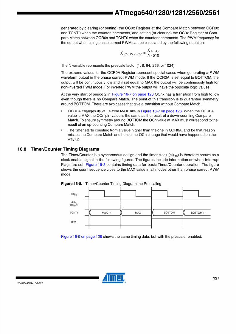
8/20/2019 At Mega 1281 Unlocked
http://slidepdf.com/reader/full/at-mega-1281-unlocked 127/446
127
2549P–AVR–10/2012
ATmega640/1280/1281/2560/2561
generated by clearing (or setting) the OC0x Register at the Compare Match between OCR0x
and TCNT0 when the counter increments, and setting (or clearing) the OC0x Register at Com-
pare Match between OCR0x and TCNT0 when the counter decrements. The PWM frequency fo
the output when using phase correct PWM can be calculated by the following equation:
The N variable represents the prescale factor (1, 8, 64, 256, or 1024).
The extreme values for the OCR0A Register represent special cases when generating a P WM
waveform output in the phase correct PWM mode. If the OCR0A is set equal to BOTTOM, the
output will be continuously low and if set equal to MAX the output will be continuously high for
non-inverted PWM mode. For inverted PWM the output will have the opposite logic values.
At the very start of period 2 in Figure 16-7 on page 126 OCnx has a transition from high to low
even though there is no Compare Match. The point of this transition is to guarantee symmetry
around BOTTOM. There are two cases that give a transition without Compare Match.
• OCR0A changes its value from MAX, like in Figure 16-7 on page 126. When the OCR0A
value is MAX the OCn pin value is the same as the result of a down-counting CompareMatch. To ensure symmetry around BOTTOM the OCn value at MAX must correspond to theresult of an up-counting Compare Match.
• The timer starts counting from a value higher than the one in OCR0A, and for that reasonmisses the Compare Match and hence the OCn change that would have happened on theway up.
16.8 Timer/Counter Timing Diagrams
The Timer/Counter is a synchronous design and the timer clock (clkT0) is therefore shown as a
clock enable signal in the following figures. The figures include information on when Interrup
Flags are set. Figure 16-8 contains timing data for basic Timer/Counter operation. The figure
shows the count sequence close to the MAX value in all modes other than phase correct PW
Mmode.
Figure 16-8. Timer/Counter Timing Diagram, no Prescaling
Figure 16-9 on page 128 shows the same timing data, but with the prescaler enabled.
f OCnxPCPWM
f clk_I/O
N 510⋅
------------------=
clkTn
(clkI/O
/1)
TOVn
clkI/O
TCNTn MAX - 1 MAX BOTTOM BOTTOM + 1

8/20/2019 At Mega 1281 Unlocked
http://slidepdf.com/reader/full/at-mega-1281-unlocked 128/446
128
2549P–AVR–10/2012
ATmega640/1280/1281/2560/2561
Figure 16-9. Timer/Counter Timing Diagram, with Prescaler (fclk_I/O /8)
Figure 16-10 shows the setting of OCF0B in all modes and OCF0A in all modes except CTC
mode and PWM mode, where OCR0A is TOP.
Figure 16-10. Timer/Counter Timing Diagram, Setting of OCF0x, with Prescaler (fclk_I/O /8)
Figure 16-11 shows the setting of OCF0A and the clearing of TCNT0 in CTC mode and fast
PWM mode where OCR0A is TOP.
Figure 16-11. Timer/Counter Timing Diagram, Clear Timer on Compare Match mode, with Pres-caler (fclk_I/O /8)
TOVn
TCNTn MAX - 1 MAX BOTTOM BOTTOM + 1
clkI/O
clkTn
(clkI/O
/ 8)
OCFnx
OCRnx
TCNTn
OCRnx Value
OCRnx - 1 OCRnx OCRnx + 1 OCRnx + 2
clkI/O
clkTn(clk
I/O / 8)
OCFnx
OCRnx
TCNTn(CTC)
TOP
TOP - 1 TOP BOTTOM BOTTOM + 1
clkI/O
clkTn
(clkI/O
/ 8)

8/20/2019 At Mega 1281 Unlocked
http://slidepdf.com/reader/full/at-mega-1281-unlocked 129/446
129
2549P–AVR–10/2012
ATmega640/1280/1281/2560/2561
16.9 Register Description
16.9.1 TCCR0A – Timer/Counter Control Register A
• Bits 7:6 – COM0A1:0: Compare Match Output A Mode
These bits control the Output Compare pin (OC0A) behavior. If one or both of the COM0A1:0
bits are set, the OC0A output overrides the normal port functionality of the I/O pin it is connected
to. However, note that the Data Direction Register (DDR) bit corresponding to the OC0A pin
must be set in order to enable the output driver.
When OC0A is connected to the pin, the function of the COM0A1:0 bits depends on the
WGM02:0 bit setting. Table 16-2 shows the COM0A1:0 bit functionality when the WGM02:0 bits
are set to a normal or CTC mode (non-PWM).
Table 16-3 shows the COM0A1:0 bit functionality when the WGM01:0 bits are set to fast PWM
mode.
Note: 1. A special case occurs when OCR0A equals TOP and COM0A1 is set. In this case, the Com-pare Match is ignored, but the set or clear is done at BOTTOM. See “Fast PWM Mode” onpage 124 for more details.
Table 16-4 on page 130 shows the COM0A1:0 bit functionality when the WGM02:0 bits are se
to phase correct PWM mode.
Bit 7 6 5 4 3 2 1 0
0x24 (0x44) COM0A1 COM0A0 COM0B1 COM0B0 – – WGM01 WGM00 TCCR0A
Read/ Write R/ W R/ W R/ W R/ W R R R/ W R/ W
Initial Value 0 0 0 0 0 0 0 0
Table 16-2. Compare Output Mode, non-PWM Mode
COM0A1 COM0A0 Description
0 0 Normal port operation, OC0A disconnected
0 1 Toggle OC0A on Compare Match
1 0 Clear OC0A on Compare Match
1 1 Set OC0A on Compare Match
Table 16-3. Compare Output Mode, Fast PWM Mode(1)
COM0A1 COM0A0 Description
0 0 Normal port operation, OC0A disconnected
0 1 WGM02 = 0: Normal Port Operation, OC0A Disconnected
WGM02 = 1: Toggle OC0A on Compare Match
1 0Clear OC0A on Compare Match, set OC0A at BOTTOM
(non-inverting mode)
1 1Set OC0A on Compare Match, clear OC0A at BOTTOM
(inverting mode)

8/20/2019 At Mega 1281 Unlocked
http://slidepdf.com/reader/full/at-mega-1281-unlocked 130/446
130
2549P–AVR–10/2012
ATmega640/1280/1281/2560/2561
Note: 1. A special case occurs when OCR0A equals TOP and COM0A1 is set. In this case, the Com-pare Match is ignored, but the set or clear is done at TOP. See “Phase Correct PWM Mode” onpage 126 for more details.
• Bits 5:4 – COM0B1:0: Compare Match Output B Mode
These bits control the Output Compare pin (OC0B) behavior. If one or both of the COM0B1:0
bits are set, the OC0B output overrides the normal port functionality of the I/O pin it is connectedto. However, note that the Data Direction Register (DDR) bit corresponding to the OC0B pin
must be set in order to enable the output driver.
When OC0B is connected to the pin, the function of the COM0B1:0 bits depends on the
WGM02:0 bit setting. Table 16-5 shows the COM0B1:0 bit functionality when the WGM02:0 bits
are set to a normal or CTC mode (non-PWM).
Table 16-6 shows the COM0B1:0 bit functionality when the WGM02:0 bits are set to fast PWM
mode.
Note: 1. A special case occurs when OCR0B equals TOP and COM0B1 is set. In this case, the Com-pare Match is ignored, but the set or clear is done at BOTTOM. See “Fast PWM Mode” onpage 124 for more details.
Table 16-4. Compare Output Mode, Phase Correct PWM Mode(1)
COM0A1 COM0A0 Description
0 0 Normal port operation, OC0A disconnected
0 1 WGM02 = 0: Normal Port Operation, OC0A DisconnectedWGM02 = 1: Toggle OC0A on Compare Match
1 0Clear OC0A on Compare Match when up-counting. Set OC0A on
Compare Match when down-counting
1 1Set OC0A on Compare Match when up-counting. Clear OC0A on
Compare Match when down-counting
Table 16-5. Compare Output Mode, non-PWM Mode
COM0B1 COM0B0 Description
0 0 Normal port operation, OC0B disconnected
0 1 Toggle OC0B on Compare Match
1 0 Clear OC0B on Compare Match
1 1 Set OC0B on Compare Match
Table 16-6. Compare Output Mode, Fast PWM Mode(1)
COM0B1 COM0B0 Description
0 0 Normal port operation, OC0B disconnected
0 1 Reserved
1 0Clear OC0B on Compare Match, set OC0B at BOTTOM
(non-inverting mode)
1 1Set OC0B on Compare Match, clear OC0B at BOTTOM
(inverting mode)
8/20/2019 At Mega 1281 Unlocked
http://slidepdf.com/reader/full/at-mega-1281-unlocked 131/446
131
2549P–AVR–10/2012
ATmega640/1280/1281/2560/2561
Table 16-7 shows the COM0B1:0 bit functionality when the WGM02:0 bits are set to phase cor-
rect PWM mode.
Note: 1. A special case occurs when OCR0B equals TOP and COM0B1 is set. In this case, the Com-pare Match is ignored, but the set or clear is done at TOP. See “Phase Correct PWM Mode” onpage 126 for more details.
• Bits 3, 2 – Res: Reserved Bits
These bits are reserved bits and will always read as zero.
• Bits 1:0 – WGM01:0: Waveform Generation Mode
Combined with the WGM02 bit found in the TCCR0B Register, these bits control the counting
sequence of the counter, the source for maximum (TOP) counter value, and what type of wave
form generation to be used, see Table 16-8. Modes of operation supported by the Timer/Counte
unit are: Normal mode (counter), Clear Timer on Compare Match (CTC) mode, and two types o
Pulse Width Modulation (PWM) modes (see “Modes of Operation” on page 148).
Note: 1. MAX = 0xFF
2. BOTTOM = 0x00
Table 16-7. Compare Output Mode, Phase Correct PWM Mode(1)
COM0B1 COM0B0 Description
0 0 Normal port operation, OC0B disconnected
0 1 Reserved
1 0Clear OC0B on Compare Match when up-counting. Set OC0B on
Compare Match when down-counting
1 1Set OC0B on Compare Match when up-counting. Clear OC0B on
Compare Match when down-counting
Table 16-8. Waveform Generation Mode Bit Description
Mode WGM2 WGM1 WGM0
Timer/Counter
Mode of
Operation TOP
Update of
OCRx at
TOV Flag
Set on(1)(2)
0 0 0 0 Normal 0xFF Immediate MAX
1 0 0 1PWM, Phase
Correct0xFF TOP BOTTOM
2 0 1 0 CTC OCRA Immediate MAX
3 0 1 1 Fast PWM 0xFF TOP MAX
4 1 0 0 Reserved – – –
5 1 0 1PWM, Phase
CorrectOCRA TOP BOTTOM
6 1 1 0 Reserved – – –
7 1 1 1 Fast PWM OCRA BOTTOM TOP

8/20/2019 At Mega 1281 Unlocked
http://slidepdf.com/reader/full/at-mega-1281-unlocked 132/446
132
2549P–AVR–10/2012
ATmega640/1280/1281/2560/2561
16.9.2 TCCR0B – Timer/Counter Control Register B
• Bit 7 – FOC0A: Force Output Compare A
The FOC0A bit is only active when the WGM bits specify a non-PWM mode.
However, for ensuring compatibility with future devices, this bit must be set to zero when
TCCR0B is written when operating in PWM mode. When writing a logical one to the FOC0A bit
an immediate Compare Match is forced on the Waveform Generation unit. The OC0A output is
changed according to its COM0A1:0 bits setting. Note that the FOC0A bit is implemented as a
strobe. Therefore it is the value present in the COM0A1:0 bits that determines the effect of the
forced compare.
A FOC0A strobe will not generate any interrupt, nor will it clear the timer in CTC mode using
OCR0A as TOP.
The FOC0A bit is always read as zero.
• Bit 6 – FOC0B: Force Output Compare B
The FOC0B bit is only active when the WGM bits specify a non-PWM mode.
However, for ensuring compatibility with future devices, this bit must be set to zero when
TCCR0B is written when operating in PWM mode. When writing a logical one to the FOC0B bit
an immediate Compare Match is forced on the Waveform Generation unit. The OC0B output is
changed according to its COM0B1:0 bits setting. Note that the FOC0B bit is implemented as a
strobe. Therefore it is the value present in the COM0B1:0 bits that determines the effect of the
forced compare.
A FOC0B strobe will not generate any interrupt, nor will it clear the timer in CTC mode using
OCR0B as TOP.
The FOC0B bit is always read as zero.
• Bits 5:4 – Res: Reserved Bits
These bits are reserved bits and will always read as zero.
• Bit 3 – WGM02: Waveform Generation Mode
See the description in the “TCCR0A – Timer/Counter Control Register A” on page 129.
• Bits 2:0 – CS02:0: Clock Select
The three Clock Select bits select the clock source to be used by the Timer/Counter, see Table
16-9 on page 133.
Bit 7 6 5 4 3 2 1 0
0x25 (0x45) FOC0A FOC0B – – WGM02 CS02 CS01 CS00 TCCR0B
Read/ Write W W R R R/ W R/ W R/ W R/ W
Initial Value 0 0 0 0 0 0 0 0

8/20/2019 At Mega 1281 Unlocked
http://slidepdf.com/reader/full/at-mega-1281-unlocked 133/446
133
2549P–AVR–10/2012
ATmega640/1280/1281/2560/2561
If external pin modes are used for the Timer/Counter0, transitions on the T0 pin will clock the
counter even if the pin is configured as an output. This feature allows software control of the
counting.
16.9.3 TCNT0 – Timer/Counter Register
The Timer/Counter Register gives direct access, both for read and write operations, to the
Timer/Counter unit 8-bit counter. Writing to the TCNT0 Register blocks (removes) the Compare
Match on the following timer clock. Modifying the counter (TCNT0) while the counter is running
introduces a risk of missing a Compare Match between TCNT0 and the OCR0x Registers.
16.9.4 OCR0A – Output Compare Register A
The Output Compare Register A contains an 8-bit value that is continuously compared with the
counter value (TCNT0). A match can be used to generate an Output Compare interrupt, or to
generate a waveform output on the OC0A pin.
16.9.5 OCR0B – Output Compare Register B
The Output Compare Register B contains an 8-bit value that is continuously compared with the
counter value (TCNT0). A match can be used to generate an Output Compare interrupt, or to
generate a waveform output on the OC0B pin.
Table 16-9. Clock Select Bit Description
CS02 CS01 CS00 Description
0 0 0 No clock source (Timer/Counter stopped)
0 0 1 clkI/O /(N
o prescaling)0 1 0 clkI/O /8 (From prescaler)
0 1 1 clkI/O /64 (From prescaler)
1 0 0 clkI/O /256 (From prescaler)
1 0 1 clkI/O /1024 (From prescaler)
1 1 0 External clock source on T0 pin. Clock on falling edge
1 1 1 External clock source on T0 pin. Clock on rising edge
Bit 7 6 5 4 3 2 1 0
0x26 (0x46) TCNT0[7:0] TCNT0
Read/ Write R/ W R/ W R/ W R/ W R/ W R/ W R/ W R/ W
Initial Value 0 0 0 0 0 0 0 0
Bit 7 6 5 4 3 2 1 0
0x27 (0x47) OCR0A[7:0] OCR0A
Read/ Write R/ W R/ W R/ W R/ W R/ W R/ W R/ W R/ W
Initial Value 0 0 0 0 0 0 0 0
Bit 7 6 5 4 3 2 1 0
0x28 (0x48) OCR0B[7:0] OCR0B
Read/ Write R/ W R/ W R/ W R/ W R/ W R/ W R/ W R/ W
Initial Value 0 0 0 0 0 0 0 0

8/20/2019 At Mega 1281 Unlocked
http://slidepdf.com/reader/full/at-mega-1281-unlocked 134/446
134
2549P–AVR–10/2012
ATmega640/1280/1281/2560/2561
16.9.6 TIMSK0 – Timer/Counter Interrupt Mask Register
• Bits 7:3, 0 – Res: Reserved BitsThese bits are reserved bits and will always read as zero.
• Bit 2 – OCIE0B: Timer/Counter Output Compare Match B Interrupt Enable
When the OCIE0B bit is written to one, and the I-bit in the Status Register is set, the
Timer/Counter Compare Match B interrupt is enabled. The corresponding interrupt is executed i
a Compare Match in Timer/Counter occurs, that is, when the OCF0B bit is set in the
Timer/Counter Interrupt Flag Register – TIFR0.
• Bit 1 – OCIE0A: Timer/Counter0 Output Compare Match A Interrupt Enable
When the OCIE0A bit is written to one, and the I-bit in the Status Register is set, the
Timer/Counter0 Compare Match A interrupt is enabled. The corresponding interrupt is executed
if a Compare Match in Timer/Counter0 occurs, that is, when the OCF0A bit is set in theTimer/Counter 0 Interrupt Flag Register – TIFR0.
• Bit 0 – TOIE0: Timer/Counter0 Overflow Interrupt Enable
When the TOIE0 bit is written to one, and the I-bit in the Status Register is set, the
Timer/Counter0 Overflow interrupt is enabled. The corresponding interrupt is executed if an
overflow in Timer/Counter0 occurs, that is, when the TOV0 bit is set in the Timer/Counter 0 Inter
rupt Flag Register – TIFR0.
16.9.7 TIFR0 – Timer/Counter 0 Interrupt Flag Register
• Bits 7:3, 0 – Res: Reserved Bits
These bits are reserved bits and will always read as zero.
• Bit 2 – OCF0B: Timer/Counter 0 Output Compare B Match Flag
The OCF0B bit is set when a Compare Match occurs between the Timer/Counter and the data in
OCR0B – Output Compare Register0 B. OCF0B is cleared by hardware when executing the cor
responding interrupt handling vector. Alternatively, OCF0B is cleared by writing a logic one to
the flag. When the I-bit in SREG, OCIE0B (Timer/Counter Compare B Match Interrupt Enable)
and OCF0B are set, the Timer/Counter Compare Match Interrupt is executed.
• Bit 1 – OCF0A: Timer/Counter 0 Output Compare A Match Flag
The OCF0A bit is set when a Compare Match occurs between the Timer/Counter0 and the data
in OCR0A – Output Compare Register0. OCF0A is cleared by hardware when executing the cor
responding interrupt handling vector. Alternatively, OCF0A is cleared by writing a logic one to
the flag. When the I-bit in SREG, OCIE0A (Timer/Counter0 Compare Match Interrupt Enable)
and OCF0A are set, the Timer/Counter0 Compare Match Interrupt is executed.
Bit 7 6 5 4 3 2 1 0
(0x6E) – – – – – OCIE0B OCIE0A TOIE0 TIMSK0
Read/ Write R R R R R R/ W R/ W R/ W
Initial Value 0 0 0 0 0 0 0 0
Bit 7 6 5 4 3 2 1 0
0x15 (0x35) – – – – – OCF0B OCF0A TOV0 TIFR0
Read/ Write R R R R R R/ W R/ W R/ W
Initial Value 0 0 0 0 0 0 0 0

8/20/2019 At Mega 1281 Unlocked
http://slidepdf.com/reader/full/at-mega-1281-unlocked 135/446
135
2549P–AVR–10/2012
ATmega640/1280/1281/2560/2561
• Bit 0 – TOV0: Timer/Counter0 Overflow Flag
The bit TOV0 is set when an overflow occurs in Timer/Counter0. TOV0 is cleared by hardware
when executing the corresponding interrupt handling vector. Alternatively, TOV0 is cleared by
writing a logic one to the flag. When the SREG I-bit, TOIE0 (Timer/Counter0 Overflow Interrup
Enable), and TOV0 are set, the Timer/Counter0 Overflow interrupt is executed.
The setting of this flag is dependent of theW
GM02:0 bit setting. Refer to Table 16-8, “W
aveformGeneration Mode Bit Description” on page 131.

8/20/2019 At Mega 1281 Unlocked
http://slidepdf.com/reader/full/at-mega-1281-unlocked 136/446
136
2549P–AVR–10/2012
ATmega640/1280/1281/2560/2561
17. 16-bit Timer/Counter (Timer/Counter 1, 3, 4, and 5)
17.1 Features
• True 16-bit Design (that is, allows 16-bit PWM)
• Three independent Output Compare Units
• Double Buffered Output Compare Registers• One Input Capture Unit
• Input Capture Noise Canceler
• Clear Timer on Compare Match (Auto Reload)
• Glitch-free, Phase Correct Pulse Width Modulator (PWM)
• Variable PWM Period
• Frequency Generator
• External Event Counter
• Twenty independent interrupt sources (TOV1, OCF1A, OCF1B, OCF1C, ICF1, TOV3, OCF3A,
OCF3B, OCF3C, ICF3, TOV4, OCF4A, OCF4B, OCF4C, ICF4, TOV5, OCF5A, OCF5B, OCF5C and
ICF5)
17.2 OverviewThe 16-bit Timer/Counter unit allows accurate program execution timing (event management)
wave generation, and signal timing measurement.
Most register and bit references in this section are written in general form. A lower case “n”
replaces the Timer/Counter number, and a lower case “x” replaces the Output Compare unit
channel. However, when using the register or bit defines in a program, the precise form must be
used, that is, TCNT1 for accessing Timer/Counter1 counter value and so on.
A simplified block diagram of the 16-bit Timer/Counter is shown in Figure 17-1 on page 137. Fo
the actual placement of I/O pins, see “TQFP-pinout ATmega640/1280/2560” on page 2 and
“Pinout ATmega1281/2561” on page 4. CPU accessible I/O Registers, including I/O bits and I/O
pins, are shown in bold. The device-specific I/O Register and bit locations are listed in the “Reg
ister Description” on page 158.
The Power Reduction Timer/Counter1 bit, PRTIM1, in “PRR0 – Power Reduction Register 0” on
page 56 must be written to zero to enable Timer/Counter1 module.
The Power Reduction Timer/Counter3 bit, PRTIM3, in “PRR1 – Power Reduction Register 1” on
page 57 must be written to zero to enable Timer/Counter3 module.
The Power Reduction Timer/Counter4 bit, PRTIM4, in “PRR1 – Power Reduction Register 1” on
page 57 must be written to zero to enable Timer/Counter4 module.
The Power Reduction Timer/Counter5 bit, PRTIM5, in “PRR1 – Power Reduction Register 1” on
page 57 must be written to zero to enable Timer/Counter5 module.
Timer/Counter4 and Timer/Counter5 only have full functionality in the ATmega640/1280/2560Input capture and output compare are not available in the ATmega1281/2561.

8/20/2019 At Mega 1281 Unlocked
http://slidepdf.com/reader/full/at-mega-1281-unlocked 137/446
137
2549P–AVR–10/2012
ATmega640/1280/1281/2560/2561
Figure 17-1. 16-bit Timer/Counter Block Diagram(1)
Note: 1. Refer to Figure 1-1 on page 2, Table 13-5 on page 79, and Table 13-11 on page 83 foTimer/Counter1 and 3 and 3 pin placement and description.
17.2.1 Registers
The Timer/Counter (TCNTn), Output Compare Registers (OCRnA/B/C), and Input Capture Reg
ister (ICRn) are all 16-bit registers. Special procedures must be followed when accessing the 16
bit registers. These procedures are described in the section “Accessing 16-bit Registers” on
page 138. The Timer/Counter Control Registers (TCCRnA/B/C) are 8-bit registers and have no
CPU access restrictions. Interrupt requests (shorten as Int.Req.) signals are all visible in the
Timer Interrupt Flag Register (TIFRn). All interrupts are individually masked with the Timer Inter
rupt Mask Register (TIMSKn). TIFRn and TIMSKn are not shown in the figure since these
registers are shared by other timer units.
The Timer/Counter can be clocked internally, via the prescaler, or by an external clock source on
the Tn pin. The Clock Select logic block controls which clock source and edge the Timer/Counte
uses to increment (or decrement) its value. The Timer/Counter is inactive when no clock source
is selected. The output from the clock select logic is referred to as the timer clock (clkTn).
The double buffered Output Compare Registers (OCRnA/B/C) are compared with the
Timer/Counter value at all time. The result of the compare can be used by the Waveform Gener
ator to generate a PWM or variable frequency output on the Output Compare pin (OCnA/B/C).
ICFn (Int.Req.)
TOVn
(Int.Req.)
Clock Select
Timer/Counter
D A
T A B U S
ICRn
=
=
=
TCNTn
Waveform
Generation
Waveform
Generation
Waveform
Generation
OCnA
OCnB
OCnC
NoiseCanceler
ICPn
=
FixedTOP
Values
EdgeDetector
Control Logic
= 0
TOP BOTTOM
Count
Clear
Direction
OCFnA
(Int.Req.)
OCFnB
(Int.Req.)
OCFnC
(Int.Req.)
TCCRnA TCCRnB TCCRnC
( From Analog
Comparator Ouput )
TnEdge
Detector
( From Prescaler )
TCLK
OCRnC
OCRnB
OCRnA

8/20/2019 At Mega 1281 Unlocked
http://slidepdf.com/reader/full/at-mega-1281-unlocked 138/446
138
2549P–AVR–10/2012
ATmega640/1280/1281/2560/2561
See “Output Compare Units” on page 145. The compare match event will also set the Compare
Match Flag (OCFnA/B/C) which can be used to generate an Output Compare interrupt request.
The Input Capture Register can capture the Timer/Counter value at a given external (edge trig-
gered) event on either the Input Capture pin (ICPn) or on the Analog Comparator pins (see “AC
– Analog Comparator” on page 271). The Input Capture unit includes a digital filtering unit
(Noise Canceler) for reducing the chance of capturing noise spikes.
The TOP value, or maximum Timer/Counter value, can in some modes of operation be defined
by either the OCRnA Register, the ICRn Register, or by a set of fixed values. When using
OCRnA as TOP value in a PWM mode, the OCRnA Register can not be used for generating a
PWM output. However, the TOP value will in this case be double buffered allowing the TOP
value to be changed in run time. If a fixed TOP value is required, the ICRn Register can be used
as an alternative, freeing the OCRnA to be used as PWM output.
17.2.2 Definitions
The following definitions are used extensively throughout the document:
17.3 Accessing 16-bit Registers
The TCNTn, OCRnA/B/C, and ICRn are 16-bit registers that can be accessed by the AVR CPU
via the 8-bit data bus. The 16-bit register must be byte accessed using two read or write opera-
tions. Each 16-bit timer has a single 8-bit register for temporary storing of the high byte of the 16
bit access. The same Temporary Register is shared between all 16-bit registers within each 16bit timer. Accessing the low byte triggers the 16-bit read or write operation. When the low byte o
a 16-bit register is written by the CPU, the high byte stored in the Temporary Register, and the
low byte written are both copied into the 16-bit register in the same clock cycle. When the low
byte of a 16-bit register is read by the CPU, the high byte of the 16-bit register is copied into the
Temporary Register in the same clock cycle as the low byte is read.
Not all 16-bit accesses uses the Temporary Register for the high byte. Reading the OCRnA/B/C
16-bit registers does not involve using the Temporary Register.
To do a 16-bit write, the high byte must be written before the low byte. For a 16-bit read, the low
byte must be read before the high byte.
The following code examples show how to access the 16-bit timer registers assuming that nointerrupts updates the temporary register. The same principle can be used directly for accessing
the OCRnA/B/C and ICRn Registers. Note that when using “C”, the compiler handles the 16-bi
access.
Table 17-1. Definitions
BOTTOM The counter reaches the BOTTOM when it becomes 0x0000.MAX The counter reaches its MAX imum when it becomes 0xFFFF (decimal 65535).
TOP The counter reaches the TOP when it becomes equal to the highest value in the
count sequence. The TOP value can be assigned to be one of the fixed values:
0x00FF, 0x01FF, or 0x03FF, or to the value stored in the OCRnA or ICRn Reg-
ister. The assignment is dependent of the mode of operation.

8/20/2019 At Mega 1281 Unlocked
http://slidepdf.com/reader/full/at-mega-1281-unlocked 139/446
139
2549P–AVR–10/2012
ATmega640/1280/1281/2560/2561
Note: 1. See “About Code Examples” on page 11.
The assembly code example returns the TCNTn value in the r17:r16 register pair.
It is important to notice that accessing 16-bit registers are atomic operations. If an interrup
occurs between the two instructions accessing the 16-bit register, and the interrupt code
updates the temporary register by accessing the same or any other of the 16-bit Timer Regis
ters, then the result of the access outside the interrupt will be corrupted. Therefore, when both
the main code and the interrupt code update the temporary register, the main code must disablethe interrupts during the 16-bit access.
The following code examples show how to do an atomic read of the TCNTn Register contents
Reading any of the OCRnA/B/C or ICRn Registers can be done by using the same principle.
Assembly Code Examples(1)
...
; Set TCNTn to 0x01FF
ldi r17,0x01
ldi r16,0xFF
out TCNTnH,r17
out TCNTnL,r16
; Read TCNTn into r17:r16
in r16,TCNTnL
in r17,TCNTnH
...
C Code Examples(1)
unsigned int i;
...
/* Set TCNTn to 0x01FF */
TCNTn = 0x1FF;/* Read TCNTn into i */
i = TCNTn;
...

8/20/2019 At Mega 1281 Unlocked
http://slidepdf.com/reader/full/at-mega-1281-unlocked 140/446
140
2549P–AVR–10/2012
ATmega640/1280/1281/2560/2561
Note: 1. See “About Code Examples” on page 11.
The assembly code example returns the TCNTn value in the r17:r16 register pair.
Assembly Code Example(1)
TIM16_ReadTCNTn:
; Save global interrupt flag
in r18,SREG
; Disable interrupts
cli
; Read TCNTn into r17:r16
in r16,TCNTnL
in r17,TCNTnH
; Restore global interrupt flag
out SREG,r18
ret
C Code Example(1)
unsigned int TIM16_ReadTCNTn( void )
{
unsigned char sreg;
unsigned int i;
/* Save global interrupt flag */
sreg = SREG;
/* Disable interrupts */
__disable_interrupt();
/* Read TCNTn into i */
i = TCNTn;
/* Restore global interrupt flag */
SREG = sreg;
return i;
}
8/20/2019 At Mega 1281 Unlocked
http://slidepdf.com/reader/full/at-mega-1281-unlocked 141/446
141
2549P–AVR–10/2012
ATmega640/1280/1281/2560/2561
The following code examples show how to do an atomic write of the TC NTn Register contents
Writing any of the OCRnA/B/C or ICRn Registers can be done by using the same principle.
Note: 1. See “About Code Examples” on page 11.
The assembly code example requires that the r17:r16 register pair contains the value to be writ-
ten to TCNTn.
17.3.1 Reusing the Temporary High Byte Register
If writing to more than one 16-bit register where the high byte is the same for all registers written
then the high byte only needs to be written once. However, note that the same rule of atomic
operation described previously also applies in this case.
17.4 Timer/Counter Clock Sources
The Timer/Counter can be clocked by an internal or an external clock source. The clock source
is selected by the Clock Select logic which is controlled by the Clock Select (CSn2:0) bits
located in the Timer/Counter control Register B (TCCRnB). For details on clock sources and
prescaler, see “Timer/Counter 0, 1, 3, 4, and 5 Prescaler” on page 169.
Assembly Code Example(1)
TIM16_WriteTCNTn:
; Save global interrupt flag
in r18,SREG
; Disable interrupts
cli
; Set TCNTn to r17:r16
out TCNTnH,r17
out TCNTnL,r16
; Restore global interrupt flag
out SREG,r18
ret
C Code Example(1)
void TIM16_WriteTCNTn( unsigned int i )
{
unsigned char sreg;
unsigned int i;
/* Save global interrupt flag */
sreg = SREG;
/* Disable interrupts */
__disable_interrupt();
/* Set TCNTn to i */
TCNTn = i;
/* Restore global interrupt flag */
SREG = sreg;
}
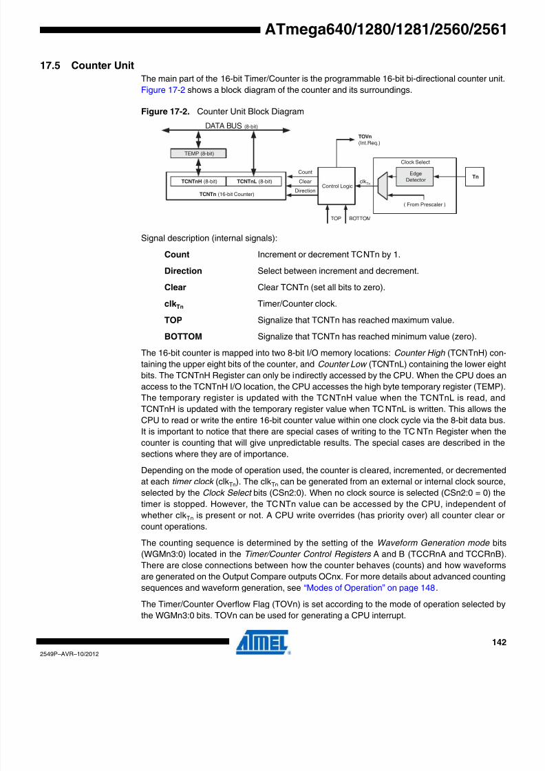
8/20/2019 At Mega 1281 Unlocked
http://slidepdf.com/reader/full/at-mega-1281-unlocked 142/446
142
2549P–AVR–10/2012
ATmega640/1280/1281/2560/2561
17.5 Counter Unit
The main part of the 16-bit Timer/Counter is the programmable 16-bit bi-directional counter unit
Figure 17-2 shows a block diagram of the counter and its surroundings.
Figure 17-2. Counter Unit Block Diagram
Signal description (internal signals):
Count Increment or decrement TCNTn by 1.
Direction Select between increment and decrement.
Clear Clear TCNTn (set all bits to zero).
clk Tn Timer/Counter clock.
TOP Signalize that TCNTn has reached maximum value.
BOTTOM Signalize that TCNTn has reached minimum value (zero).
The 16-bit counter is mapped into two 8-bit I/O memory locations: Counter High (TCNTnH) con
taining the upper eight bits of the counter, and Counter Low (TCNTnL) containing the lower eigh
bits. The TCNTnH Register can only be indirectly accessed by the CPU. When the CPU does an
access to the TCNTnH I/O location, the CPU accesses the high byte temporary register (TEMP)
The temporary register is updated with the TCNTnH value when the TCNTnL is read, andTCNTnH is updated with the temporary register value when TC NTnL is written. This allows the
CPU to read or write the entire 16-bit counter value within one clock cycle via the 8-bit data bus
It is important to notice that there are special cases of writing to the TCNTn Register when the
counter is counting that will give unpredictable results. The special cases are described in the
sections where they are of importance.
Depending on the mode of operation used, the counter is cleared, incremented, or decremented
at each timer clock (clkTn). The clkTn can be generated from an external or internal clock source
selected by the Clock Select bits (CSn2:0). When no clock source is selected (CSn2:0 = 0) the
timer is stopped. However, the TCNTn value can be accessed by the CPU, independent of
whether clkTn is present or not. A CPU write overrides (has priority over) all counter clear or
count operations.
The counting sequence is determined by the setting of the Waveform Generation mode bits
(WGMn3:0) located in the Timer/Counter Control Registers A and B (TCCRnA and TCCRnB)
There are close connections between how the counter behaves (counts) and how waveforms
are generated on the Output Compare outputs OCnx. For more details about advanced counting
sequences and waveform generation, see “Modes of Operation” on page 148.
The Timer/Counter Overflow Flag (TOVn) is set according to the mode of operation selected by
the WGMn3:0 bits. TOVn can be used for generating a CPU interrupt.
TEMP (8-bit)
DATA BUS (8-bit)
TCNTn (16-bit Counter)
TCNTnH (8-bit) TCNTnL (8-bit)Control Logic
Count
Clear
Direction
TOVn
(Int.Req.)
Clock Select
TOP BOTTOM
TnEdge
Detector
( From Prescaler )
clkTn

8/20/2019 At Mega 1281 Unlocked
http://slidepdf.com/reader/full/at-mega-1281-unlocked 143/446
143
2549P–AVR–10/2012
ATmega640/1280/1281/2560/2561
17.6 Input Capture Unit
The Timer/Counter incorporates an input capture unit that can capture external events and give
them a time-stamp indicating time of occurrence. The external signal indicating an event, or mul
tiple events, can be applied via the ICPn pin or alternatively, for the Timer/Counter1 only, via the
Analog Comparator unit. The time-stamps can then be used to calculate frequency, duty-cycle
and other features of the signal applied. Alternatively the time-stamps can be used for creating a
log of the events.
The Input Capture unit is illustrated by the block diagram shown in Figure 17-3. The elements o
the block diagram that are not directly a part of the input capture unit are gray shaded. The smal
“n” in register and bit names indicates the Timer/Counter number.
Figure 17-3. Input Capture Unit Block Diagram
Note: The Analog Comparator Output (ACO) can only trigger the Timer/Counter1 ICP – notTimer/Counter3, 4 or 5.
When a change of the logic level (an event) occurs on the Input Capture Pin (ICPn), alternatively
on the analog Comparator output (ACO), and this change confirms to the setting of the edge
detector, a capture will be triggered. When a capture is triggered, the 16-bit value of the counte
(TCNTn) is written to the Input Capture Register (ICRn). The Input Capture Flag (ICFn) is set a
the same system clock as the TCNTn value is copied into ICRn Register. If enabled (TICIEn =
1), the input capture flag generates an input capture interrupt. The ICFn flag is automatically
cleared when the interrupt is executed. Alternatively the ICFn flag can be cleared by software bywriting a logical one to its I/O bit location.
Reading the 16-bit value in the Input Capture Register (ICRn) is done by first reading the low
byte (ICRnL) and then the high byte (ICRnH). When the low byte is read the high byte is copied
into the high byte Temporary Register (TEMP). When the CPU reads the ICRnH I/O location it
will access the TEMP Register.
ICFn (Int.Req.)
Analog
Comparator
WRITE ICRn (16-bit Register)
ICRnH (8-bit)
NoiseCancelerICPn
EdgeDetector
TEMP (8-bit)
DATA BUS (8-bit)
ICRnL (8-bit)
TCNTn (16-bit Counter)
TCNTnH (8-bit) TCNTnL (8-bit)
ACIC* ICNC ICESACO*

8/20/2019 At Mega 1281 Unlocked
http://slidepdf.com/reader/full/at-mega-1281-unlocked 144/446
144
2549P–AVR–10/2012
ATmega640/1280/1281/2560/2561
The ICRn Register can only be written when using a Waveform Generation mode that utilizes
the ICRn Register for defining the counter’s TOP value. In these cases the Waveform Genera
tion mode (WGMn3:0) bits must be set before the TOP value can be written to the ICRn
Register. When writing the ICRn Register the high byte must be written to the ICRnH I/O location
before the low byte is written to ICRnL.
For more information on how to access the 16-bit registers refer to “Accessing 16-bit Registers”
on page 138.
17.6.1 Input Capture Trigger Source
The main trigger source for the input capture unit is the Input Capture Pin (ICPn).
Timer/Counter1 can alternatively use the analog comparator output as trigger source for the
input capture unit. The Analog Comparator is selected as trigger source by setting the analog
Comparator Input Capture (ACIC) bit in the Analog Comparator Control and Status Registe
(ACSR). Be aware that changing trigger source can trigger a capture. The input capture flag
must therefore be cleared after the change.
Both the Input Capture Pin (ICPn) and the Analog Comparator output (ACO) inputs are sampled
using the same technique as for the Tn pin (Figure 18-1 on page 169). The edge detector is also
identical. However, when the noise canceler is enabled, additional logic is inserted before theedge detector, which increases the delay by four system clock cycles. Note that the input of the
noise canceler and edge detector is always enabled unless the Timer/Counter is set in a Wave
form Generation mode that uses ICRn to define TOP.
An input capture can be triggered by software by controlling the port of the ICPn pin.
17.6.2 Noise Canceler
The noise canceler improves noise immunity by using a simple digital filtering scheme. The
noise canceler input is monitored over four samples, and all four must be equal for changing the
output that in turn is used by the edge detector.
The noise canceler is enabled by setting the Input Capture Noise Canceler (ICNCn) bit in
Timer/Counter Control Register B (TCCRnB). When enabled the noise canceler introduces addi-
tional four system clock cycles of delay from a change applied to the input, to the update of the
ICRn Register. The noise canceler uses the system clock and is therefore not affected by the
prescaler.
17.6.3 Using the Input Capture Unit
The main challenge when using the Input Capture unit is to assign enough processor capacity
for handling the incoming events. The time between two events is critical. If the processor has
not read the captured value in the ICRn Register before the next event occurs, the ICRn will be
overwritten with a new value. In this case the result of the capture will be incorrect.
When using the Input Capture interrupt, the ICRn Register should be read as early in the inter-
rupt handler routine as possible. Even though the Input Capture interrupt has relatively highpriority, the maximum interrupt response time is dependent on the maximum number of clock
cycles it takes to handle any of the other interrupt requests.
Using the Input Capture unit in any mode of operation when the TOP value (resolution) is
actively changed during operation, is not recommended.
Measurement of an external signal’s duty cycle requires that the trigger edge is changed afte
each capture. Changing the edge sensing must be done as early as possible after the ICRn

8/20/2019 At Mega 1281 Unlocked
http://slidepdf.com/reader/full/at-mega-1281-unlocked 145/446
145
2549P–AVR–10/2012
ATmega640/1280/1281/2560/2561
Register has been read. After a change of the edge, the Input Capture Flag (ICFn) must be
cleared by software (writing a logical one to the I/O bit location). For measuring frequency only,
the clearing of the ICFn Flag is not required (if an interrupt handler is used).
17.7 Output Compare Units
The 16-bit comparator continuously compares TCNTn with the Output Compare Register
(OCRnx). If TCNT equals OCRnx the comparator signals a match. A match will set the Outpu
Compare Flag (OCFnx) at the next timer clock cycle. If enabled (OCIEnx = 1), the Output Com
pare Flag generates an Output Compare interrupt. The OCFnx Flag is automatically cleared
when the interrupt is executed. Alternatively the OCFnx Flag can be cleared by software by writ
ing a logical one to its I/O bit location. The Waveform Generator uses the match signal to
generate an output according to operating mode set by the Waveform Generation mode
(WGMn3:0) bits and Compare Output mode (COMnx1:0) bits. The TOP and BOTTOM signals
are used by the Waveform Generator for handling the special cases of the extreme values in
some modes of operation. See “Modes of Operation” on page 148.
A special feature of Output Compare unit A allows it to define the Timer/Counter TOP value (tha
is, counter resolution). In addition to the counter resolution, the TOP value defines the period
time for waveforms generated by the Waveform Generator.
Figure 17-4 shows a block diagram of the Output Compare unit. The small “n” in the register and
bit names indicates the device number (n = n for Timer/Counter n), and the “x” indicates Outpu
Compare unit (A/B/C). The elements of the block diagram that are not directly a part of the Out
put Compare unit are gray shaded.
Figure 17-4. Output Compare Unit, Block Diagram
OCFnx (Int.Req.)
= (16-bit Comparator )
OCRnx Buffer (16-bit Register)
OCRnxH Buf. (8-bit)
OCnx
TEMP (8-bit)
DATA BUS (8-bit)
OCRnxL Buf. (8-bit)
TCNTn (16-bit Counter)
TCNTnH (8-bit) TCNTnL (8-bit)
COMnx1:0WGMn3:0
OCRnx (16-bit Register)
OCRnxH (8-bit) OCRnxL (8-bit)
Waveform GeneratorTOP
BOTTOM

8/20/2019 At Mega 1281 Unlocked
http://slidepdf.com/reader/full/at-mega-1281-unlocked 146/446
146
2549P–AVR–10/2012
ATmega640/1280/1281/2560/2561
The OCRnx Register is double buffered when using any of the twelve Pulse Width Modulation
(PWM) modes. For the Normal and Clear Timer on Compare (CTC) modes of operation, the
double buffering is disabled. The double buffering synchronizes the update of the OCRnx Com-
pare Register to either TOP or BOTTOM of the counting sequence. The synchronization
prevents the occurrence of odd-length, non-symmetrical PWM pulses, thereby making the out
put glitch-free.
The OCRnx Register access may seem complex, but this is not case. When the double buffering
is enabled, the CPU has access to the OCRnx Buffer Register, and if double buffering is dis-
abled the CPU will access the OCRnx directly. The content of the OCR1x (Buffer or Compare)
Register is only changed by a write operation (the Timer/Counter does not update this registe
automatically as the TCNT1 and ICR1 Register). Therefore OCR1x is not read via the high byte
temporary register (TEMP). However, it is a good practice to read the low byte first as when
accessing other 16-bit registers. Writing the OCRnx Registers must be done via the TEMP Reg
ister since the compare of all 16 bits is done continuously. The high byte (OCRnxH) has to be
written first. When the high byte I/O location is written by the CPU, the TEMP Register will be
updated by the value written. Then when the low byte (OCRnxL) is written to the lower eight bits
the high byte will be copied into the upper 8-bits of either the OCRnx buffer or OCRnx Compare
Register in the same system clock cycle.For more information of how to access the 16-bit registers refer to “Accessing 16-bit Registers
on page 138.
17.7.1 Force Output Compare
In non-PWM Waveform Generation modes, the match output of the comparator can be forced by
writing a one to the Force Output Compare (FOCnx) bit. Forcing compare match will not set the
OCFnx Flag or reload/clear the timer, but the OCnx pin will be updated as if a real compare
match had occurred (the COMn1:0 bits settings define whether the OCnx pin is set, cleared or
toggled).
17.7.2 Compare Match Blocking by TCNTn Write
All CPU writes to the TCNTn Register will block any compare match that occurs in the next time
clock cycle, even when the timer is stopped. This feature allows OCRnx to be initialized to the
same value as TCNTn without triggering an interrupt when the Timer/Counter clock is enabled.
17.7.3 Using the Output Compare Unit
Since writing TCNTn in any mode of operation will block all compare matches for one timer clock
cycle, there are risks involved when changing TCNTn when using any of the Output Compare
channels, independent of whether the Timer/Counter is running or not. If the value written to
TCNTn equals the OCRnx value, the compare match will be missed, resulting in incorrect wave
form generation. Do not write the TCNTn equal to TOP in PWM modes with variable TOP
values. The compare match for the TOP will be ignored and the counter will continue to 0xFFFF
Similarly, do not write the TCN
Tn value equal to BOTTOM when the counter is downcounting.The setup of the OCnx should be performed before setting the Data Direction Register for the
port pin to output. The easiest way of setting the OCnx value is to use the Force Output Com
pare (FOCnx) strobe bits in Normal mode. The OCnx Register keeps its value even when
changing between Waveform Generation modes.
Be aware that the COMnx1:0 bits are not double buffered together with the compare value.
Changing the COMnx1:0 bits will take effect immediately.

8/20/2019 At Mega 1281 Unlocked
http://slidepdf.com/reader/full/at-mega-1281-unlocked 147/446
147
2549P–AVR–10/2012
ATmega640/1280/1281/2560/2561
17.8 Compare Match Output Unit
The Compare Output mode (COMnx1:0) bits have two functions. The Waveform Generator uses
the COMnx1:0 bits for defining the Output Compare (OCnx) state at the next compare match
Secondly the COMnx1:0 bits control the OCnx pin output source. Figure 17-5 shows a simplified
schematic of the logic affected by the COMnx1:0 bit setting. The I/O Registers, I/O bits, and I/O
pins in the figure are shown in bold. Only the parts of the general I/O Port Control Registers
(DDR and PORT) that are affected by the COMnx1:0 bits are shown. When referring to theOCnx state, the reference is for the internal OCnx Register, not the OCnx pin. If a system reset
occur, the OCnx Register is reset to “0”.
Figure 17-5. Compare Match Output Unit, Schematic
The general I/O port function is overridden by the Output Compare (OCnx) from the Waveform
Generator if either of the COMnx1:0 bits are set. However, the OCnx pin direction (input or out-
put) is still controlled by the Data Direction Register (DDR) for the port pin. The Data Direction
Register bit for the OCnx pin (DDR_OCnx) must be set as output before the OCnx value is visi-
ble on the pin. The port override function is generally independent of the Waveform Generation
mode, but there are some exceptions. Refer to Table 17-3 on page 159, Table 17-4 on page 159
and Table 17-5 on page 160 for details.
The design of the Output Compare pin logic allows initialization of the OCnx state before the out
put is enabled. Note that some COMnx1:0 bit settings are reserved for certain modes of
operation. See “Register Description” on page 158.
The COMnx1:0 bits have no effect on the Input Capture unit.
17.8.1 Compare Output Mode and Waveform Generation
The Waveform Generator uses the COMnx1:0 bits differently in normal, CTC, and PWM modes
For all modes, setting the COMnx1:0 = 0 tells the Waveform Generator that no action on the
OCnx Register is to be performed on the next compare match. For compare output actions in the
PORT
DDR
D Q
D Q
OCnx
PinOCnx
D QWaveform
Generator
COMnx1
COMnx0
0
1
DATA
BU
S
FOCnx
clkI/O

8/20/2019 At Mega 1281 Unlocked
http://slidepdf.com/reader/full/at-mega-1281-unlocked 148/446
148
2549P–AVR–10/2012
ATmega640/1280/1281/2560/2561
non-PWM modes refer to Table 17-3 on page 159. For fast PWM mode refer to Table 17-4 on
page 159, and for phase correct and phase and frequency correct PWM refer to Table 17-5 on
page 160.
A change of the COMnx1:0 bits state will have effect at the first compare match after the bits are
written. For non-PWM modes, the action can be forced to have immediate effect by using the
FOCnx strobe bits.
17.9 Modes of Operation
The mode of operation, that is, the behavior of the Timer/Counter and the Output Compare pins
is defined by the combination of the Waveform Generation mode (WGMn3:0) and Compare Out
put mode (COMnx1:0) bits. The Compare Output mode bits do not affect the counting sequence
while the Waveform Generation mode bits do. The COMnx1:0 bits control whether the PWM out
put generated should be inverted or not (inverted or non-inverted PWM). For non-PWM modes
the COMnx1:0 bits control whether the output should be set, cleared or toggle at a compare
match. See “Compare Match Output Unit” on page 147.
Note: 1. The CTCn and PWMn1:0 bit definition names are obsolete. Use the WGMn2:0 definitions.However, the functionality and location of these bits are compatible with previous versions ofthe timer.
For detailed timing information refer to “Timer/Counter Timing Diagrams” on page 156.
Table 17-2. Waveform Generation Mode Bit Description(1)
Mode WGMn3WGMn2(CTCn)
WGMn1(PWMn1)
WGMn0(PWMn0)
Timer/CounterMode of Operation TOP
Update ofOCRnx at
TOVn FlagSet on
0 0 0 0 0 Normal 0xFFFF Immediate MAX
1 0 0 0 1 PWM, Phase Correct, 8-bit 0x00FF TOP BOTTOM
2 0 0 1 0 PWM, Phase Correct, 9-bit 0x01FF TOP BOTTOM
3 0 0 1 1 PWM, Phase Correct, 10-bit 0x03FF TOP BOTTOM
4 0 1 0 0 CTC OCRnA Immediate MAX
5 0 1 0 1 Fast PWM, 8-bit 0x00FF BOTTOM TOP
6 0 1 1 0 Fast PWM, 9-bit 0x01FF BOTTOM TOP
7 0 1 1 1 Fast PWM, 10-bit 0x03FF BOTTOM TOP
8 1 0 0 0PWM, Phase and Frequency
CorrectICRn BOTTOM BOTTOM
9 1 0 0 1PWM,Phase and Frequency
CorrectOCRnA BOTTOM BOTTOM
10 1 0 1 0 PWM, Phase Correct ICRn TOP BOTTOM
11 1 0 1 1 PWM, Phase Correct OCRnA TOP BOTTOM
12 1 1 0 0 CTC ICRn Immediate MAX
13 1 1 0 1 (Reserved) – – –
14 1 1 1 0 Fast PWM ICRn BOTTOM TOP
15 1 1 1 1 Fast PWM OCRnA BOTTOM TOP

8/20/2019 At Mega 1281 Unlocked
http://slidepdf.com/reader/full/at-mega-1281-unlocked 149/446
149
2549P–AVR–10/2012
ATmega640/1280/1281/2560/2561
17.9.1 Normal Mode
The simplest mode of operation is the Normal mode (WGMn3:0 = 0). In this mode the counting
direction is always up (incrementing), and no counter clear is performed. The counter simply
overruns when it passes its maximum 16-bit value (MAX = 0xFFFF) and then restarts from the
BOTTOM (0x0000). In normal operation the Timer/Counter Overflow Flag (TOVn) will be set in
the same timer clock cycle as the TCNTn becomes zero. The TOVn Flag in this case behaves
like a 17th bit, except that it is only set, not cleared. However, combined with the timer overflowinterrupt that automatically clears the TOVn Flag, the timer resolution can be increased by soft-
ware. There are no special cases to consider in the Normal mode, a new counter value can be
written anytime.
The Input Capture unit is easy to use in Normal mode. However, observe that the maximum
interval between the external events must not exceed the resolution of the counter. If the interva
between events are too long, the timer overflow interrupt or the prescaler must be used to
extend the resolution for the capture unit.
The Output Compare units can be used to generate interrupts at some given time. Using the
Output Compare to generate waveforms in Normal mode is not recommended, since this wil
occupy too much of the CPU time.
17.9.2 Clear Timer on Compare Match (CTC) Mode
In Clear Timer on Compare or CTC mode (WGMn3:0 = 4 or 12), the OCRnA or ICRn Register
are used to manipulate the counter resolution. In CTC mode the counter is cleared to zero when
the counter value (TCNTn) matches either the OCRnA (WGMn3:0 = 4) or the ICRn (WGMn3:0 =
12). The OCRnA or ICRn define the top value for the counter, hence also its resolution. This
mode allows greater control of the compare match output frequency. It also simplifies the opera
tion of counting external events.
The timing diagram for the CTC mode is shown in Figure 17-6. The counter value (TCNTn)
increases until a compare match occurs with either OCRnA or ICRn, and then counter (TCNTn
is cleared.
Figure 17-6. CTC Mode, Timing Diagram
An interrupt can be generated at each time the counter value reaches the TOP value by either
using the OCFnA or ICFn Flag according to the register used to define the TOP value. If the
interrupt is enabled, the interrupt handler routine can be used for updating the TOP value. How
ever, changing the TOP to a value close to BOTTOM when the counter is running with none or a
low prescaler value must be done with care since the CTC mode does not have the double buff
ering feature. If the new value written to OCRnA or ICRn is lower than the current value of
TCNTn
OCnA(Toggle)
OCnA Interrupt Flag Setor ICFn Interrupt Flag Set(Interrupt on TOP)
1 4Period 2 3
(COMnA1:0 = 1)

8/20/2019 At Mega 1281 Unlocked
http://slidepdf.com/reader/full/at-mega-1281-unlocked 150/446
150
2549P–AVR–10/2012
ATmega640/1280/1281/2560/2561
TCNTn, the counter will miss the compare match. The counter will then have to count to its max
imum value (0xFFFF) and wrap around starting at 0x0000 before the compare match can occur
In many cases this feature is not desirable. An alternative will then be to use the fast PWM mode
using OCRnA for defining TOP (WGMn3:0 = 15) since the OCRnA then will be double buffered.
For generating a waveform output in CTC mode, the OCnA output can be set to toggle its logica
level on each compare match by setting the Compare Output mode bits to toggle mode
(COMnA1:0 = 1). The OCnA value will not be visible on the port pin unless the data direction for
the pin is set to output (DDR_OCnA = 1). The waveform generated will have a maximum fre
quency of fOCnA = fclk_I/O /2 when OCRnA is set to zero (0x0000). The waveform frequency is
defined by the following equation:
The N variable represents the prescaler factor (1, 8, 64, 256, or 1024).
As for the Normal mode of operation, the TOVn Flag is set in the same timer clock cycle that the
counter counts from MAX to 0x0000.
17.9.3 Fast PWM Mode
The fast Pulse Width Modulation or fast PWM mode (WGMn3:0 = 5, 6, 7, 14, or 15) provides a
high frequency PWM waveform generation option. The fast PWM differs from the other PWM
options by its single-slope operation. The counter counts from BOTTOM to TOP then restarts
from BOTTOM. In non-inverting Compare Output mode, the Output Compare (OCnx) is cleared
on the compare match between TCNTn and OCRnx, and set at BOTTOM. In inverting Compare
Output mode output is set on compare match and cleared at BOTTOM. Due to the single-slope
operation, the operating frequency of the fast PWM mode can be twice as high as the phase cor-
rect and phase and frequency correct PWM modes that use dual-slope operation. This high
frequency makes the fast PWM mode well suited for power regulation, rectification, and DAC
applications. High frequency allows physically small sized external components (coils, capaci-
tors), hence reduces total system cost.The PWM resolution for fast PWM can be fixed to 8-bit, 9-bit, or 10-bit, or defined by either ICRn
or OCRnA. The minimum resolution allowed is 2-bit (ICRn or OCRnA set to 0x0003), and the
maximum resolution is 16-bit (ICRn or OCRnA set to MAX). The PWM resolution in bits can be
calculated by using the following equation:
In fast PWM mode the counter is incremented until the counter value matches either one of the
fixed values 0x00FF, 0x01FF, or 0x03FF (WGMn3:0 = 5, 6, or 7), the value in ICRn (WGMn3:0 =
14), or the value in OCRnA (WGMn3:0 = 15). The counter is then cleared at the following time
clock cycle. The timing diagram for the fast PWM mode is shown in Figure 17-7 on page 151
The figure shows fast PWM mode when OCRnA or ICRn is used to define TOP. The TC NTnvalue is in the timing diagram shown as a histogram for illustrating the single-slope operation
The diagram includes non-inverted and inverted PWM outputs. The small horizontal line marks
on the TCNTn slopes represent compare matches between OCRnx and TCNTn. The OCnx
Interrupt Flag will be set when a compare match occurs.
f OCnA
f clk_I/O
2 N 1 OCRnA+( )⋅ ⋅---------------------------------------------------=
R FP WM TO P 1+( )log
2( )log-----------------------------------=
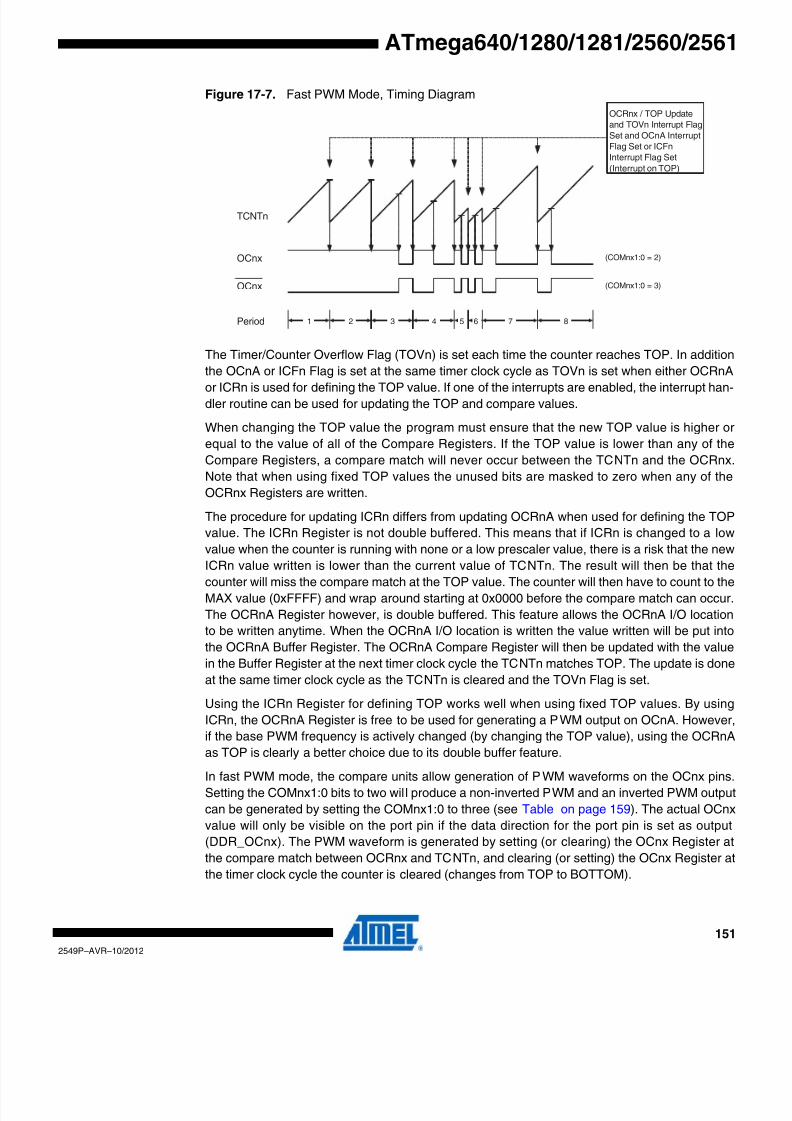
8/20/2019 At Mega 1281 Unlocked
http://slidepdf.com/reader/full/at-mega-1281-unlocked 151/446
151
2549P–AVR–10/2012
ATmega640/1280/1281/2560/2561
Figure 17-7. Fast PWM Mode, Timing Diagram
The Timer/Counter Overflow Flag (TOVn) is set each time the counter reaches TOP. In addition
the OCnA or ICFn Flag is set at the same timer clock cycle as TOVn is set when either OCRnA
or ICRn is used for defining the TOP value. If one of the interrupts are enabled, the interrupt han-dler routine can be used for updating the TOP and compare values.
When changing the TOP value the program must ensure that the new TOP value is higher o
equal to the value of all of the Compare Registers. If the TOP value is lower than any of the
Compare Registers, a compare match will never occur between the TCNTn and the OCRnx
Note that when using fixed TOP values the unused bits are masked to zero when any of the
OCRnx Registers are written.
The procedure for updating ICRn differs from updating OCRnA when used for defining the TOP
value. The ICRn Register is not double buffered. This means that if ICRn is changed to a low
value when the counter is running with none or a low prescaler value, there is a risk that the new
ICRn value written is lower than the current value of TCNTn. The result will then be that the
counter will miss the compare match at the TOP value. The counter will then have to count to the
MAX value (0xFFFF) and wrap around starting at 0x0000 before the compare match can occur
The OCRnA Register however, is double buffered. This feature allows the OCRnA I/O location
to be written anytime. When the OCRnA I/O location is written the value written will be put into
the OCRnA Buffer Register. The OCRnA Compare Register will then be updated with the value
in the Buffer Register at the next timer clock cycle the TCNTn matches TOP. The update is done
at the same timer clock cycle as the TCNTn is cleared and the TOVn Flag is set.
Using the ICRn Register for defining TOP works well when using fixed TOP values. By using
ICRn, the OCRnA Register is free to be used for generating a PWM output on OCnA. However
if the base PWM frequency is actively changed (by changing the TOP value), using the OCRnA
as TOP is clearly a better choice due to its double buffer feature.
In fast PWM mode, the compare units allow generation of PWM waveforms on the OCnx pins
Setting the COMnx1:0 bits to two will produce a non-inverted PWM and an inverted PWM outpu
can be generated by setting the COMnx1:0 to three (see Table on page 159). The actual OCnx
value will only be visible on the port pin if the data direction for the port pin is set as output
(DDR_OCnx). The PWM waveform is generated by setting (or clearing) the OCnx Register at
the compare match between OCRnx and TCNTn, and clearing (or setting) the OCnx Register a
the timer clock cycle the counter is cleared (changes from TOP to BOTTOM).
TCNTn
OCRnx / TOP Updateand TOVn Interrupt FlagSet and OCnA InterruptFlag Set or ICFnInterrupt Flag Set
(Interrupt on TOP)
1 7Period 2 3 4 5 6 8
OCnx
OCnx
(COMnx1:0 = 2)
(COMnx1:0 = 3)
8/20/2019 At Mega 1281 Unlocked
http://slidepdf.com/reader/full/at-mega-1281-unlocked 152/446
152
2549P–AVR–10/2012
ATmega640/1280/1281/2560/2561
The PWM frequency for the output can be calculated by the following equation:
The N variable represents the prescaler divider (1, 8, 64, 256, or 1024).
The extreme values for the OCRnx Register represents special cases when generating a P WMwaveform output in the fast PWM mode. If the OCRnx is set equal to BOTTOM (0x0000) the out-
put will be a narrow spike for each TOP+1 timer clock cycle. Setting the OCRnx equal to TOP
will result in a constant high or low output (depending on the polarity of the output set by the
COMnx1:0 bits).
A frequency (with 50% duty cycle) waveform output in fast PWM mode can be achieved by set
ting OCnA to toggle its logical level on each compare match (COMnA1:0 = 1). This applies only
if OCR1A is used to define the TOP value (WGM13:0 = 15). The waveform generated will have
a maximum frequency of fOCnA = fclk_I/O /2 when OCRnA is set to zero (0x0000). This feature is
similar to the OCnA toggle in CTC mode, except the double buffer feature of the Output Com-
pare unit is enabled in the fast PWM mode.
17.9.4 Phase Correct PWM Mode
The phase correct Pulse Width Modulation or phase correct PWM mode (WGMn3:0 = 1, 2, 3
10, or 11) provides a high resolution phase correct PWM waveform generation option. The
phase correct PWM mode is, like the phase and frequency correct PWM mode, based on a dual
slope operation. The counter counts repeatedly from BOTTOM (0x0000) to TOP and then from
TOP to BOTTOM. In non-inverting Compare Output mode, the Output Compare (OCnx) is
cleared on the compare match between TCNTn and OCRnx while upcounting, and set on the
compare match while downcounting. In inverting Output Compare mode, the operation is
inverted. The dual-slope operation has lower maximum operation frequency than single slope
operation. However, due to the symmetric feature of the dual-slope PWM modes, these modes
are preferred for motor control applications.
The PWM resolution for the phase correct PWM mode can be fixed to 8-bit, 9-bit, or 10-bit, o
defined by either ICRn or OCRnA. The minimum resolution allowed is 2-bit (ICRn or OCRnA se
to 0x0003), and the maximum resolution is 16-bit (ICRn or OCRnA set to MAX). The PWM reso
lution in bits can be calculated by using the following equation:
In phase correct PWM mode the counter is incremented until the counter value matches eithe
one of the fixed values 0x00FF, 0x01FF, or 0x03FF (WGMn3:0 = 1, 2, or 3), the value in ICRn
(WGMn3:0 = 10), or the value in OCRnA (WGMn3:0 = 11). The counter has then reached the
TOP and changes the count direction. The TCNTn value will be equal to TOP for one timer clock
cycle. The timing diagram for the phase correct PWM mode is shown on Figure 17-8 on page153. The figure shows phase correct PWM mode when OCRnA or ICRn is used to define TOP
The TCNTn value is in the timing diagram shown as a histogram for illustrating the dual-slope
operation. The diagram includes non-inverted and inverted PWM outputs. The small horizonta
line marks on the TCNTn slopes represent compare matches between OCRnx and TCNTn. The
OCnx Interrupt Flag will be set when a compare match occurs.
f OCnxPWM
f clk_I/O
N 1 TO P +( )⋅-----------------------------------=
R PC PW M TO P 1+( )log
2( )log-----------------------------------=

8/20/2019 At Mega 1281 Unlocked
http://slidepdf.com/reader/full/at-mega-1281-unlocked 153/446
153
2549P–AVR–10/2012
ATmega640/1280/1281/2560/2561
Figure 17-8. Phase Correct PWM Mode, Timing Diagram
The Timer/Counter Overflow Flag (TOVn) is set each time the counter reaches BOTTOM. When
either OCRnA or ICRn is used for defining the TOP value, the OCnA or ICFn Flag is set accord-
ingly at the same timer clock cycle as the OCRnx Registers are updated with the double buffer
value (at TOP). The Interrupt Flags can be used to generate an interrupt each time the counte
reaches the TOP or BOTTOM value.
When changing the TOP value the program must ensure that the new TOP value is higher o
equal to the value of all of the Compare Registers. If the TOP value is lower than any of the
Compare Registers, a compare match will never occur between the TCNTn and the OCRnx
Note that when using fixed TOP values, the unused bits are masked to zero when any of the
OCRnx Registers are written. As the third period shown in Figure 17-8 illustrates, changing the
TOP actively while the Timer/Counter is running in the phase correct mode can result in anunsymmetrical output. The reason for this can be found in the time of update of the OCRnx Reg
ister. Since the OCRnx update occurs at TOP, the PWM period starts and ends at TOP. This
implies that the length of the falling slope is determined by the previous TOP value, while the
length of the rising slope is determined by the new TOP value. When these two values differ the
two slopes of the period will differ in length. The difference in length gives the unsymmetrica
result on the output.
It is recommended to use the phase and frequency correct mode instead of the phase correc
mode when changing the TOP value while the Timer/Counter is running. When using a static
TOP value there are practically no differences between the two modes of operation.
In phase correct PWM mode, the compare units allow generation of PWM waveforms on the
OCnx pins. Setting the COMnx1:0 bits to two will produce a non-inverted PWM and an inverted
PWM output can be generated by setting the COMnx1:0 to three (see Table 17-5 on page 160)
The actual OCnx value will only be visible on the port pin if the data direction for the port pin is
set as output (DDR_OCnx). The PWM waveform is generated by setting (or clearing) the OCnx
Register at the compare match between OCRnx and TCNTn when the counter increments, and
clearing (or setting) the OCnx Register at compare match between OCRnx and TCNTn when
OCRnx/TOP Update andOCnA Interrupt Flag Setor ICFn Interrupt Flag Set(Interrupt on TOP)
1 2 3 4
TOVn Interrupt FlagS
et(Interrupt on Bottom)
TCNTn
Period
OCnx
OCnx
(COMnx1:0 = 2)
(COMnx1:0 = 3)

8/20/2019 At Mega 1281 Unlocked
http://slidepdf.com/reader/full/at-mega-1281-unlocked 154/446
154
2549P–AVR–10/2012
ATmega640/1280/1281/2560/2561
the counter decrements. The PWM frequency for the output when using phase correct PWM can
be calculated by the following equation:
TheN
variable represents the prescaler divider (1, 8, 64, 256, or 1024).The extreme values for the OCRnx Register represent special cases when generating a PWM
waveform output in the phase correct PWM mode. If the OCRnx is set equal to BOTTOM the
output will be continuously low and if set equal to TOP the output will be continuously high fo
non-inverted PWM mode. For inverted PWM the output will have the opposite logic values. If
OCR1A is used to define the TOP value (WGM13:0 = 11) and COM1A1:0 = 1, the OC1A outpu
will toggle with a 50% duty cycle.
17.9.5 Phase and Frequency Correct PWM Mode
The phase and frequency correct Pulse Width Modulation, or phase and frequency correct PWM
mode (WGMn3:0 = 8 or 9) provides a high resolution phase and frequency correct P WM wave
form generation option. The phase and frequency correct PWM mode is, like the phase correc
PWM mode, based on a dual-slope operation. The counter counts repeatedly from BOTTOM
(0x0000) to TOP and then from TOP to BOTTOM. In non-inverting Compare Output mode, the
Output Compare (OCnx) is cleared on the compare match between TCNTn and OCRnx while
upcounting, and set on the compare match while downcounting. In inverting Compare Outpu
mode, the operation is inverted. The dual-slope operation gives a lower maximum operation fre
quency compared to the single-slope operation. However, due to the symmetric feature of the
dual-slope PWM modes, these modes are preferred for motor control applications.
The main difference between the phase correct, and the phase and frequency correct P WM
mode is the time the OCRnx Register is updated by the OCRnx Buffer Register, see Figure 17-8
on page 153 and Figure 17-9 on page 155.
The PWM resolution for the phase and frequency correct PWM mode can be defined by eithe
ICRn or OCRnA. The minimum resolution allowed is 2-bit (ICRn or OCRnA set to 0x0003), and
the maximum resolution is 16-bit (ICRn or OCRnA set to MAX). The PWM resolution in bits can
be calculated using the following equation:
In phase and frequency correct PWM mode the counter is incremented until the counter value
matches either the value in ICRn (WGMn3:0 = 8), or the value in OCRnA (WGMn3:0 = 9). The
counter has then reached the TOP and changes the count direction. The TC NTn value will be
equal to TOP for one timer clock cycle. The timing diagram for the phase correct and frequency
correct PWM mode is shown on Figure 17-9 on page 155. The figure shows phase and fre-
quency correct PWM mode when OCRnA or ICRn is used to define TOP. The TCNTn value is in
the timing diagram shown as a histogram for illustrating the dual-slope operation. The diagram
includes non-inverted and inverted PWM outputs. The small horizontal line marks on the TCNTn
slopes represent compare matches between OCRnx and TCNTn. The OCnx Interrupt Flag wil
be set when a compare match occurs.
f OCnxPCPWM
f clk_I/O
2 N TO P ⋅ ⋅----------------------------=
R PF CP WM TO P 1+( )log
2( )log-----------------------------------=

8/20/2019 At Mega 1281 Unlocked
http://slidepdf.com/reader/full/at-mega-1281-unlocked 155/446
155
2549P–AVR–10/2012
ATmega640/1280/1281/2560/2561
Figure 17-9. Phase and Frequency Correct PWM Mode, Timing Diagram
The Timer/Counter Overflow Flag (TOVn) is set at the same timer clock cycle as the OCRnx
Registers are updated with the double buffer value (at BOTTOM). When either OCRnA or ICRn
is used for defining the TOP value, the OCnA or ICFn Flag set when TCNTn has reached TOP
The Interrupt Flags can then be used to generate an interrupt each time the counter reaches the
TOP or BOTTOM value.
When changing the TOP value the program must ensure that the new TOP value is higher o
equal to the value of all of the Compare Registers. If the TOP value is lower than any of the
Compare Registers, a compare match will never occur between the TCNTn and the OCRnx.
As Figure 17-9 shows the output generated is, in contrast to the phase correct mode, symmetri
cal in all periods. Since the OCRnx Registers are updated at BOTTOM, the length of the rising
and the falling slopes will always be equal. This gives symmetrical output pulses and is thereforefrequency correct.
Using the ICRn Register for defining TOP works well when using fixed TOP values. By using
ICRn, the OCRnA Register is free to be used for generating a PWM output on OCnA. However
if the base PWM frequency is actively changed by changing the TOP value, using the OCRnA as
TOP is clearly a better choice due to its double buffer feature.
In phase and frequency correct PWM mode, the compare units allow generation of PWM wave
forms on the OCnx pins. Setting the COMnx1:0 bits to two will produce a non-inverted PWM and
an inverted PWM output can be generated by setting the COMnx1:0 to three (see Table 17-5 on
page 160). The actual OCnx value will only be visible on the port pin if the data direction for the
port pin is set as output (DDR_OCnx). The PWM waveform is generated by setting (or clearing)
the OCnx Register at the compare match between OCRnx and TCNTn when the counter incre-ments, and clearing (or setting) the OCnx Register at compare match between OCRnx and
TCNTn when the counter decrements. The PWM frequency for the output when using phase
and frequency correct PWM can be calculated by the following equation:
The N variable represents the prescaler divider (1, 8, 64, 256, or 1024).
OCRnx/TOP UpdateandTOVn Interrupt Flag Set(Interrupt on Bottom)
OCnA Interrupt Flag Setor ICFn Interrupt Flag Set(Interrupt on TOP)
1 2 3 4
TCNTn
Period
OCnx
OCnx
(COMnx1:0 = 2)
(COMnx1:0 = 3)
f OCnxPFCPWM
f clk_I/O
2 N T OP ⋅ ⋅----------------------------=

8/20/2019 At Mega 1281 Unlocked
http://slidepdf.com/reader/full/at-mega-1281-unlocked 156/446
156
2549P–AVR–10/2012
ATmega640/1280/1281/2560/2561
The extreme values for the OCRnx Register represents special cases when generating a P WM
waveform output in the phase correct PWM mode. If the OCRnx is set equal to BOTTOM the
output will be continuously low and if set equal to TOP the output will be set to high for non-
inverted PWM mode. For inverted PWM the output will have the opposite logic values. If OCR1A
is used to define the TOP value (WGM13:0 = 9) and COM1A1:0 = 1, the OC1A output will toggle
with a 50% duty cycle.
17.10 Timer/Counter Timing Diagrams
The Timer/Counter is a synchronous design and the timer clock (clkTn) is therefore shown as a
clock enable signal in the following figures. The figures include information on when Interrup
Flags are set, and when the OCRnx Register is updated with the OCRnx buffer value (only for
modes utilizing double buffering). Figure 17-10 shows a timing diagram for the setting of OCFnx.
Figure 17-10. Timer/Counter Timing Diagram, Setting of OCFnx, no Prescaling
Figure 17-11 shows the same timing data, but with the prescaler enabled.
Figure 17-11. Timer/Counter Timing Diagram, Setting of OCFnx, with Prescaler (fclk_I/O /8)
clkTn(clk
I/O /1)
OCFnx
clkI/O
OCRnx
TCNTn
OCRnx Value
OCRnx - 1 OCRnx OCRnx + 1 OCRnx + 2
OCFnx
OCRnx
TCNTn
OCRnx Value
OCRnx - 1 OCRnx OCRnx + 1 OCRnx + 2
clkI/O
clkTn
(clkI/O
/ 8)

8/20/2019 At Mega 1281 Unlocked
http://slidepdf.com/reader/full/at-mega-1281-unlocked 157/446
157
2549P–AVR–10/2012
ATmega640/1280/1281/2560/2561
Figure 17-12 shows the count sequence close to TOP in various modes. When using phase and
frequency correct PWM mode the OCRnx Register is updated at BOTTOM. The timing diagrams
will be the same, but TOP should be replaced by BOTTOM, TOP-1 by BOTTOM+1 and so on
The same renaming applies for modes that set the TOVn Flag at BOTTOM.
Figure 17-12. Timer/Counter Timing Diagram, no Prescaling
Figure 17-13 shows the same timing data, but with the prescaler enabled.
Figure 17-13. Timer/Counter Timing Diagram, with Prescaler (fclk_I/O /8)
TOVn (FPWM)
and ICFn (if usedas TOP)
OCRnx(Update at TOP)
TCNTn(CTC and FPWM)
TCNTn(PC and PFC PWM)
TOP - 1 TOP TOP - 1 TOP - 2
Old OCRnx Value New OCRnx Value
TOP - 1 TOP BOTTOM BOTTOM + 1
clkTn
(clkI/O
/1)
clkI/O
TOVn(FPWM)
and ICFn (if used
as TOP)
OCRnx(Update at TOP)
TCNTn(CTC and FPWM)
TCNTn(PC and PFC PWM)
TOP - 1 TOP TOP - 1 TOP - 2
Old OCRnx Value New OCRnx Value
TOP - 1 TOP BOTTOM BOTTOM + 1
clkI/O
clkTn(clk
I/O / 8)

8/20/2019 At Mega 1281 Unlocked
http://slidepdf.com/reader/full/at-mega-1281-unlocked 158/446
158
2549P–AVR–10/2012
ATmega640/1280/1281/2560/2561
17.11 Register Description
17.11.1 TCCR1A – Timer/Counter 1 Control Register A
17.11.2 TCCR3A – Timer/Counter 3 Control Register A
17.11.3 TCCR4A – Timer/Counter 4 Control Register A
17.11.4 TCCR5A – Timer/Counter 5 Control Register A
• Bit 7:6 – COMnA1:0: Compare Output Mode for Channel A
• Bit 5:4 – COMnB1:0: Compare Output Mode for Channel B
• Bit 3:2 – COMnC1:0: Compare Output Mode for Channel C
The COMnA1:0, COMnB1:0, and COMnC1:0 control the output compare pins (OCnA, OCnB
and OCnC respectively) behavior. If one or both of the COMnA1:0 bits are written to one, the
OCnA output overrides the normal port functionality of the I/O pin it is connected to. If one or
both of the COMnB1:0 bits are written to one, the OCnB output overrides the normal port func-
tionality of the I/O pin it is connected to. If one or both of the COMnC1:0 bits are written to one,
the OCnC output overrides the normal port functionality of the I/O pin it is connected to. How-
ever, note that the Data Direction Register (DDR) bit corresponding to the OCnA, OCnB or
OCnC pin must be set in order to enable the output driver.
When the OCnA, OCnB or OCnC is connected to the pin, the function of the COMnx1:0 bits is
dependent of the WGMn3:0 bits setting. Table 17-3 on page 159 shows the COMnx1:0 bit func
tionality when the WGMn3:0 bits are set to a normal or a CTC mode (non-PWM).
Bit 7 6 5 4 3 2 1 0
(0x80) COM1A1 COM1A0 COM1B1 COM1B0 COM1C1 COM1C0 WGM11 WGM10 TCCR1A
Read/ Write R/ W R/ W R/ W R/ W R/ W R/ W R/ W R/ W
Initial Value 0 0 0 0 0 0 0 0
Bit 7 6 5 4 3 2 1 0
(0x90) COM3A1 COM3A0 COM3B1 COM3B0 COM3C1 COM3C0 WGM31 WGM30 TCCR3A
Read/ Write R/ W R/ W R/ W R/ W R/ W R/ W R/ W R/ W
Initial Value 0 0 0 0 0 0 0 0
Bit 7 6 5 4 3 2 1 0
(0xA0) COM4A1 COM4A0 COM4B1 COM4B0 COM4C1 COM4C0 WGM41 WGM40 TCCR4A
Read/ Write R/ W R/ W R/ W R/ W R/ W R/ W R/ W R/ W
Initial Value 0 0 0 0 0 0 0 0
Bit 7 6 5 4 3 2 1 0
(0x120) COM5A1 COM5A0 COM5B1 COM5B0 COM5C1 COM5C0 WGM51 WGM50 TCCR5A
Read/ Write R/ W R/ W R/ W R/ W R/ W R/ W R/ W R/ W
Initial Value 0 0 0 0 0 0 0 0
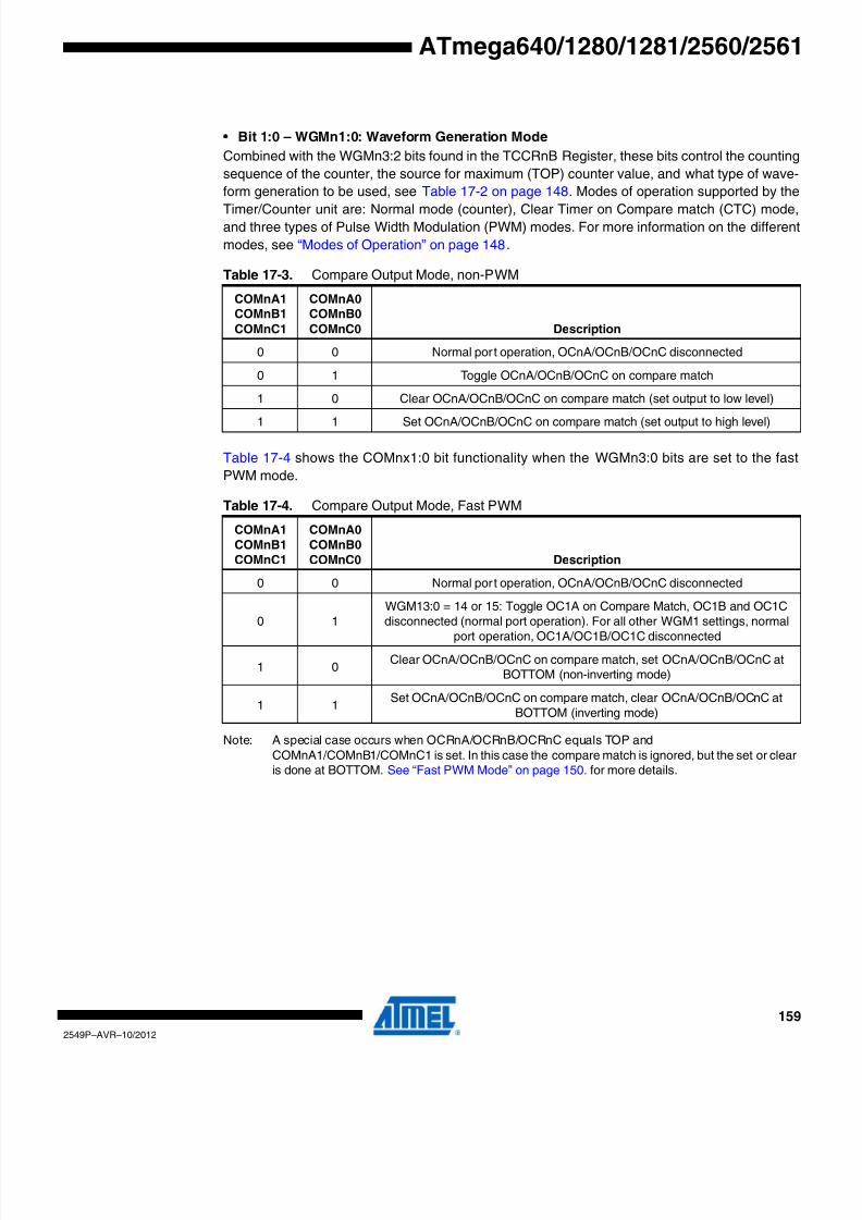
8/20/2019 At Mega 1281 Unlocked
http://slidepdf.com/reader/full/at-mega-1281-unlocked 159/446
159
2549P–AVR–10/2012
ATmega640/1280/1281/2560/2561
• Bit 1:0 – WGMn1:0: Waveform Generation Mode
Combined with the WGMn3:2 bits found in the TCCRnB Register, these bits control the counting
sequence of the counter, the source for maximum (TOP) counter value, and what type of wave
form generation to be used, see Table 17-2 on page 148. Modes of operation supported by the
Timer/Counter unit are: Normal mode (counter), Clear Timer on Compare match (CTC) modeand three types of Pulse Width Modulation (PWM) modes. For more information on the differen
modes, see “Modes of Operation” on page 148.
Table 17-4 shows the COMnx1:0 bit functionality when the WGMn3:0 bits are set to the fast
PWM mode.
Note: A special case occurs when OCRnA/OCRnB/OCRnC equals TOP andCOMnA1/COMnB1/COMnC1 is set. In this case the compare match is ignored, but the set or clearis done at BOTTOM. See “Fast PWM Mode” on page 150. for more details.
Table 17-3. Compare Output Mode, non-PWM
COMnA1
COMnB1
COMnC1
COMnA0
COMnB0
COMnC0 Description
0 0 Normal port operation, OCnA/OCnB/OCnC disconnected
0 1 Toggle OCnA/OCnB/OCnC on compare match
1 0 Clear OCnA/OCnB/OCnC on compare match (set output to low level)
1 1 Set OCnA/OCnB/OCnC on compare match (set output to high level)
Table 17-4. Compare Output Mode, Fast PWM
COMnA1
COMnB1
COMnC1
COMnA0
COMnB0
COMnC0 Description
0 0 Normal port operation, OCnA/OCnB/OCnC disconnected
0 1
WGM13:0 = 14 or 15: Toggle OC1A on Compare Match, OC1B and OC1C
disconnected (normal port operation). For all otherW
GM1 settings, normalport operation, OC1A/OC1B/OC1C disconnected
1 0Clear OCnA/OCnB/OCnC on compare match, set OCnA/OCnB/OCnC at
BOTTOM (non-inverting mode)
1 1Set OCnA/OCnB/OCnC on compare match, clear OCnA/OCnB/OCnC at
BOTTOM (inverting mode)

8/20/2019 At Mega 1281 Unlocked
http://slidepdf.com/reader/full/at-mega-1281-unlocked 160/446
160
2549P–AVR–10/2012
ATmega640/1280/1281/2560/2561
Table 17-5 shows the COMnx1:0 bit functionality when the WGMn3:0 bits are set to the phase
correct and frequency correct PWM mode.
Note: A special case occurs when OCRnA/OCRnB/OCRnC equals TOP andCOMnA1/COMnB1//COMnC1 is set. See “Phase Correct PWM Mode” on page 152. for moredetails.
17.11.5 TCCR1B – Timer/Counter 1 Control Register B
17.11.6 TCCR3B – Timer/Counter 3 Control Register B
17.11.7 TCCR4B – Timer/Counter 4 Control Register B
17.11.8 TCCR5B – Timer/Counter 5 Control Register B
• Bit 7 – ICNCn: Input Capture Noise Canceler
Setting this bit (to one) activates the Input Capture Noise Canceler. When the Noise Canceler is
activated, the input from the Input Capture Pin (ICPn) is filtered. The filter function requires four
successive equal valued samples of the ICPn pin for changing its output. The input capture is
therefore delayed by four Oscillator cycles when the noise canceler is enabled.
Table 17-5. Compare Output Mode, Phase Correct and Phase and Frequency Correct PWM
COMnA1
COMnB1
COMnC1
COMnA0
COMnB0
COMnC0 Description
0 0 Normal port operation, OCnA/OCnB/OCnC disconnected
0 1WGM13:0 =9 or 11: Toggle OC1A on Compare Match, OC1B and OC1C
disconnected (normal port operation). For all other WGM1 settings, normalport operation, OC1A/OC1B/OC1C disconnected
1 0Clear OCnA/OCnB/OCnC on compare match when up-countingSet OCnA/OCnB/OCnC on compare match when downcounting
1 1Set OCnA/OCnB/OCnC on compare match when up-counting
Clear OCnA/OCnB/OCnC on compare match when downcounting
Bit 7 6 5 4 3 2 1 0
(0x81) ICNC1 ICES1 – WGM13 WGM12 CS12 CS11 CS10 TCCR1B
Read/ Write R/ W R/ W R R/ W R/ W R/ W R/ W R/ W
Initial Value 0 0 0 0 0 0 0 0
Bit 7 6 5 4 3 2 1 0
(0x91) ICNC3 ICES3 – WGM33 WGM32 CS32 CS31 CS30 TCCR3B
Read/ Write R/ W R/ W R R/ W R/ W R/ W R/ W R/ W
Initial Value 0 0 0 0 0 0 0 0
Bit 7 6 5 4 3 2 1 0
(0xA1) ICNC4 ICES4 – WGM43 WGM42 CS42 CS41 CS40 TCCR4B
Read/ Write R/ W R/ W R R/ W R/ W R/ W R/ W R/ W
Initial Value 0 0 0 0 0 0 0 0
Bit 7 6 5 4 3 2 1 0
(0x121) ICNC5 ICES5 – WGM53 WGM52 CS52 CS51 CS50 TCCR5B
Read/ Write R/ W R/ W R R/ W R/ W R/ W R/ W R/ W
Initial Value 0 0 0 0 0 0 0 0

8/20/2019 At Mega 1281 Unlocked
http://slidepdf.com/reader/full/at-mega-1281-unlocked 161/446
161
2549P–AVR–10/2012
ATmega640/1280/1281/2560/2561
• Bit 6 – ICESn: Input Capture Edge Select
This bit selects which edge on the Input Capture Pin (ICPn) that is used to trigger a capture
event. When the ICESn bit is written to zero, a falling (negative) edge is used as trigger, and
when the ICESn bit is written to one, a rising (positive) edge will trigger the capture.
When a capture is triggered according to the ICESn setting, the counter value is copied into the
Input Capture Register (ICRn). The event will also set the Input Capture Flag (ICFn), and thiscan be used to cause an Input Capture Interrupt, if this interrupt is enabled.
When the ICRn is used as TOP value (see description of the WGMn3:0 bits located in the
TCCRnA and the TCCRnB Register), the ICPn is disconnected and consequently the input cap-
ture function is disabled.
• Bit 5 – Reserved Bit
This bit is reserved for future use. For ensuring compatibility with future devices, this bit must be
written to zero when TCCRnB is written.
• Bit 4:3 – WGMn3:2: Waveform Generation Mode
See TCCRnA Register description.
• Bit 2:0 – CSn2:0: Clock Select
The three clock select bits select the clock source to be used by the Timer/Counter, see Figure
17-10 on page 156 and Figure 17-11 on page 156.
If external pin modes are used for the Timer/Countern, transitions on the Tn pin will clock the
counter even if the pin is configured as an output. This feature allows software control of the
counting.
17.11.9 TCCR1C – Timer/Counter 1 Control Register C
Table 17-6. Clock Select Bit Description
CSn2 CSn1 CSn0 Description
0 0 0 No clock source. (Timer/Counter stopped)
0 0 1 clkI/O /1 (No prescaling
0 1 0 clkI/O /8 (From prescaler)
0 1 1 clkI/O /64 (From prescaler)
1 0 0 clkI/O /256 (From prescaler)
1 0 1 clkI/O /1024 (From prescaler)
1 1 0 External clock source on Tn pin. Clock on falling edge
1 1 1 External clock source on Tn pin. Clock on rising edge
Bit 7 6 5 4 3 2 1 0
(0x82) FOC1A FOC1B FOC1C – – – – – TCCR1C
Read/ Write W W W R R R R R
Initial Value 0 0 0 0 0 0 0 0

8/20/2019 At Mega 1281 Unlocked
http://slidepdf.com/reader/full/at-mega-1281-unlocked 162/446
162
2549P–AVR–10/2012
ATmega640/1280/1281/2560/2561
17.11.10 TCCR3C – Timer/Counter 3 Control Register C
17.11.11 TCCR4C – Timer/Counter 4 Control Register C
17.11.12 TCCR5C – Timer/Counter 5 Control Register C
• Bit 7 – FOCnA: Force Output Compare for Channel A
• Bit 6 – FOCnB: Force Output Compare for Channel B
• Bit 5 – FOCnC: Force Output Compare for Channel C
The FOCnA/FOCnB/FOCnC bits are only active when the WGMn3:0 bits specifies a non-PWM
mode. When writing a logical one to the FOCnA/FOCnB/FOCnC bit, an immediate compare
match is forced on the waveform generation unit. The OCnA/OCnB/OCnC output is changed
according to its COMnx1:0 bits setting. Note that the FOCnA/FOCnB/FOCnC bits are imple-
mented as strobes. Therefore it is the value present in the COMnx1:0 bits that determine the
effect of the forced compare.
A FOCnA/FOCnB/FOCnC strobe will not generate any interrupt nor will it clear the timer in Clea
Timer on Compare Match (CTC) mode using OCRnA as TOP.
The FOCnA/FOCnB/FOCnB bits are always read as zero.
• Bit 4:0 – Reserved Bits
These bits are reserved for future use. For ensuring compatibility with future devices, these bits
must be written to zero when TCCRnC is written.
17.11.13 TCNT1H and TCNT1L – Timer/Counter 1
17.11.14 TCNT3H and TCNT3L – Timer/Counter 3
Bit 7 6 5 4 3 2 1 0
(0x92) FOC3A FOC3B FOC3C – – – – – TCCR3C
Read/ Write W W W R R R R R
Initial Value 0 0 0 0 0 0 0 0
Bit 7 6 5 4 3 2 1 0
(0xA2) FOC4A FOC4B FOC4C – – – – – TCCR4C
Read/ Write W W W R R R R R
Initial Value 0 0 0 0 0 0 0 0
Bit 7 6 5 4 3 2 1 0
(0x122) FOC5A FOC5B FOC3C – – – – – TCCR5C
Read/ Write W W W R R R R R
Initial Value 0 0 0 0 0 0 0 0
Bit 7 6 5 4 3 2 1 0
(0x85) TCNT1[15:8] TCNT1H
(0x84) TCNT1[7:0] TCNT1L
Read/ Write R/ W R/ W R/ W R/ W R/ W R/ W R/ W R/ W
Initial Value 0 0 0 0 0 0 0 0
Bit 7 6 5 4 3 2 1 0
(0x95) TCNT3[15:8] TCNT3H
(0x94) TCNT3[7:0] TCNT3L
Read/ Write R/ W R/ W R/ W R/ W R/ W R/ W R/ W R/ W
Initial Value 0 0 0 0 0 0 0 0

8/20/2019 At Mega 1281 Unlocked
http://slidepdf.com/reader/full/at-mega-1281-unlocked 163/446
163
2549P–AVR–10/2012
ATmega640/1280/1281/2560/2561
17.11.15 TCNT4H and TCNT4L –Timer/Counter 4
17.11.16 TCNT5H and TCNT5L –Timer/Counter 5
The two Timer/Counter I/O locations (TCNTnH and TCNTnL, combined TCNTn) give direct
access, both for read and for write operations, to the Timer/Counter unit 16-bit counter. To
ensure that both the high and low bytes are read and written simultaneously when the CPU
accesses these registers, the access is performed using an 8-bit temporary High Byte Registe
(TEMP). This temporary register is shared by all the other 16-bit registers. See “Accessing 16-bi
Registers” on page 138.
Modifying the counter (TCNTn) while the counter is running introduces a risk of missing a com-
pare match between TCNTn and one of the OCRnx Registers.
Writing to the TCNTn Register blocks (removes) the compare match on the following timer clock
for all compare units.
17.11.17 OCR1AH and OCR1AL – Output Compare Register 1 A
17.11.18 OCR1BH and OCR1BL – Output Compare Register 1 B
17.11.19 OCR1CH and OCR1CL – Output Compare Register 1 C
Bit 7 6 5 4 3 2 1 0
(0xA5) TCNT4[15:8] TCNT4H
(0xA4) TCNT4[7:0] TCNT4L
Read/ Write R/ W R/ W R/ W R/ W R/ W R/ W R/ W R/ W
Initial Value 0 0 0 0 0 0 0 0
Bit 7 6 5 4 3 2 1 0
(0x125) TCNT5[15:8] TCNT5H
(0x124) TCNT5[7:0] TCNT5L
Read/ Write R/ W R/ W R/ W R/ W R/ W R/ W R/ W R/ W
Initial Value 0 0 0 0 0 0 0 0
Bit 7 6 5 4 3 2 1 0
(0x89) OCR1A[15:8] OCR1AH
(0x88) OCR1A[7:0] OCR1AL
Read/ Write R/ W R/ W R/ W R/ W R/ W R/ W R/ W R/ W
Initial Value 0 0 0 0 0 0 0 0
Bit 7 6 5 4 3 2 1 0
(0x8B) OCR1B[15:8] OCR1BH
(0x8A) OCR1B[7:0] OCR1BL
Read/ Write R/ W R/ W R/ W R/ W R/ W R/ W R/ W R/ W
Initial Value 0 0 0 0 0 0 0 0
Bit 7 6 5 4 3 2 1 0
(0x8D) OCR1C[15:8] OCR1CH
(0x8C) OCR1C[7:0] OCR1CL
Read/ Write R/ W R/ W R/ W R/ W R/ W R/ W R/ W R/ W
Initial Value 0 0 0 0 0 0 0 0
8/20/2019 At Mega 1281 Unlocked
http://slidepdf.com/reader/full/at-mega-1281-unlocked 164/446
164
2549P–AVR–10/2012
ATmega640/1280/1281/2560/2561
17.11.20 OCR3AH and OCR3AL – Output Compare Register 3 A
17.11.21 OCR3BH and OCR3BL – Output Compare Register 3 B
17.11.22 OCR3CH and OCR3CL – Output Compare Register 3 C
17.11.23 OCR4AH and OCR4AL – Output Compare Register 4 A
17.11.24 OCR4BH and OCR4BL – Output Compare Register 4 B
17.11.25 OCR4CH and OCR4CL –Output Compare Register 4 C
17.11.26 OCR5AH and OCR5AL – Output Compare Register 5 A
Bit 7 6 5 4 3 2 1 0
(0x99) OCR3A[15:8] OCR3AH
(0x98) OCR3A[7:0] OCR3AL
Read/ Write R/ W R/ W R/ W R/ W R/ W R/ W R/ W R/ W
Initial Value 0 0 0 0 0 0 0 0
Bit 7 6 5 4 3 2 1 0
(0x9B) OCR3B[15:8] OCR3BH
(0x9A) OCR3B[7:0] OCR3BL
Read/ Write R/ W R/ W R/ W R/ W R/ W R/ W R/ W R/ W
Initial Value 0 0 0 0 0 0 0 0
Bit 7 6 5 4 3 2 1 0
(0x9D) OCR3C[15:8] OCR3CH
(0x9C) OCR3C[7:0] OCR3CL
Read/ Write R/ W R/ W R/ W R/ W R/ W R/ W R/ W R/ WInitial Value 0 0 0 0 0 0 0 0
Bit 7 6 5 4 3 2 1 0
(0xA9) OCR4A[15:8] OCR4AH
(0xA8) OCR4A[7:0] OCR4AL
Read/ Write R/ W R/ W R/ W R/ W R/ W R/ W R/ W R/ W
Initial Value 0 0 0 0 0 0 0 0
Bit 7 6 5 4 3 2 1 0
(0xAA) OCR4B[15:8] OCR4BH(0xAB) OCR4B[7:0] OCR4BL
Read/ Write R/ W R/ W R/ W R/ W R/ W R/ W R/ W R/ W
Initial Value 0 0 0 0 0 0 0 0
Bit 7 6 5 4 3 2 1 0
(0xAD) OCR4C[15:8] OCR4CH
(0xAC) OCR4C[7:0] OCR4CL
Read/ Write R/ W R/ W R/ W R/ W R/ W R/ W R/ W R/ W
Initial Value 0 0 0 0 0 0 0 0
Bit 7 6 5 4 3 2 1 0
(0x129) OCR5A[15:8] OCR5AH
(0x128) OCR5A[7:0] OCR5AL
Read/ Write R/ W R/ W R/ W R/ W R/ W R/ W R/ W R/ W
Initial Value 0 0 0 0 0 0 0 0

8/20/2019 At Mega 1281 Unlocked
http://slidepdf.com/reader/full/at-mega-1281-unlocked 165/446
165
2549P–AVR–10/2012
ATmega640/1280/1281/2560/2561
17.11.27 OCR5BH and OCR5BL – Output Compare Register 5 B
17.11.28 OCR5CH and OCR5CL –Output Compare Register 5 C
The Output Compare Registers contain a 16-bit value that is continuously compared with the
counter value (TCNTn). A match can be used to generate an Output Compare interrupt, or to
generate a waveform output on the OCnx pin.
The Output Compare Registers are 16-bit in size. To ensure that both the high and low bytes are
written simultaneously when the CPU writes to these registers, the access is performed using an8-bit temporary High Byte Register (TEMP). This temporary register is shared by all the othe
16-bit registers. See “Accessing 16-bit Registers” on page 138.
17.11.29 ICR1H and ICR1L – Input Capture Register 1
17.11.30 ICR3H and ICR3L – Input Capture Register 3
17.11.31 ICR4H and ICR4L – Input Capture Register 4
17.11.32 ICR5H and ICR5L – Input Capture Register 5
Bit 7 6 5 4 3 2 1 0
(0x12B) OCR5B[15:8] OCR5BH
(0x12A) OCR5B[7:0] OCR5BL
Read/ Write R/ W R/ W R/ W R/ W R/ W R/ W R/ W R/ W
Initial Value 0 0 0 0 0 0 0 0
Bit 7 6 5 4 3 2 1 0
(0x12D) OCR5C[15:8] OCR5CH
(0x12C) OCR5C[7:0] OCR5CL
Read/ Write R/ W R/ W R/ W R/ W R/ W R/ W R/ W R/ W
Initial Value 0 0 0 0 0 0 0 0
Bit 7 6 5 4 3 2 1 0
(0x87) ICR1[15:8] ICR1H
(0x86) ICR1[7:0] ICR1L
Read/ Write R/ W R/ W R/ W R/ W R/ W R/ W R/ W R/ W
Initial Value 0 0 0 0 0 0 0 0
Bit 7 6 5 4 3 2 1 0
(0x97) ICR3[15:8] ICR3H
(0x96) ICR3[7:0] ICR3L
Read/ Write R/ W R/ W R/ W R/ W R/ W R/ W R/ W R/ W
Initial Value 0 0 0 0 0 0 0 0
Bit 7 6 5 4 3 2 1 0
(0xA7) ICR4[15:8] ICR4H
(0xA6) ICR4[7:0] ICR4L
Read/ Write R/ W R/ W R/ W R/ W R/ W R/ W R/ W R/ W
Initial Value 0 0 0 0 0 0 0 0
Bit 7 6 5 4 3 2 1 0
(0x127) ICR5[15:8] ICR5H
(0x126) ICR5[7:0] ICR5L
Read/ Write R/ W R/ W R/ W R/ W R/ W R/ W R/ W R/ W
Initial Value 0 0 0 0 0 0 0 0

8/20/2019 At Mega 1281 Unlocked
http://slidepdf.com/reader/full/at-mega-1281-unlocked 166/446
166
2549P–AVR–10/2012
ATmega640/1280/1281/2560/2561
The Input Capture is updated with the counter (TCNTn) value each time an event occurs on the
ICPn pin (or optionally on the Analog Comparator output for Timer/Counter1). The Input Capture
can be used for defining the counter TOP value.
The Input Capture Register is 16-bit in size. To ensure that both the high and low bytes are read
simultaneously when the CPU accesses these registers, the access is performed using an 8-bi
temporary High Byte Register (TEMP). This temporary register is shared by all the other 16-bit
registers. See “Accessing 16-bit Registers” on page 138.
17.11.33 TIMSK1 – Timer/Counter 1 Interrupt Mask Register
17.11.34 TIMSK3 – Timer/Counter 3 Interrupt Mask Register
17.11.35 TIMSK4 – Timer/Counter 4 Interrupt Mask Register
17.11.36 TIMSK5 – Timer/Counter 5 Interrupt Mask Register
• Bit 5 – ICIEn: Timer/Countern, Input Capture Interrupt Enable
When this bit is written to one, and the I-flag in the Status Register is set (interrupts globally
enabled), the Timer/Countern Input Capture interrupt is enabled. The corresponding Interrup
Vector (see “Interrupts” on page 105) is executed when the ICFn Flag, located in TIFRn, is set.
• Bit 3 – OCIEnC: Timer/Countern, Output Compare C Match Interrupt Enable
When this bit is written to one, and the I-flag in the Status Register is set (interrupts globally
enabled), the Timer/Countern Output Compare C Match interrupt is enabled. The correspondingInterrupt Vector (see “Interrupts” on page 105) is executed when the OCFnC Flag, located in
TIFRn, is set.
• Bit 2 – OCIEnB: Timer/Countern, Output Compare B Match Interrupt Enable
When this bit is written to one, and the I-flag in the Status Register is set (interrupts globally
enabled), the Timer/Countern Output Compare B Match interrupt is enabled. The corresponding
Interrupt Vector (see “Interrupts” on page 105) is executed when the OCFnB Flag, located in
TIFRn, is set.
Bit 7 6 5 4 3 2 1 0
(0x6F) – – ICIE1 – OCIE1C OCIE1B OCIE1A TOIE1 TIMSK1
Read/ Write R R R/ W R R/ W R/ W R/ W R/ W
Initial Value 0 0 0 0 0 0 0 0
Bit 7 6 5 4 3 2 1 0
(0x71) – – ICIE3 – OCIE3C OCIE3B OCIE3A TOIE3 TIMSK3
Read/ Write R R R/ W R R/ W R/ W R/ W R/ W
Initial Value 0 0 0 0 0 0 0 0
Bit 7 6 5 4 3 2 1 0
(0x72) – – ICIE4 – OCIE4C OCIE4B OCIE4A TOIE4 TIMSK4
Read/ Write R R R/ W R R/ W R/ W R/ W R/ W
Initial Value 0 0 0 0 0 0 0 0
Bit 7 6 5 4 3 2 1 0
(0x73) – – ICIE5 – OCIE5C OCIE5B OCIE5A TOIE5 TIMSK5
Read/ Write R R R/ W R R/ W R/ W R/ W R/ W
Initial Value 0 0 0 0 0 0 0 0

8/20/2019 At Mega 1281 Unlocked
http://slidepdf.com/reader/full/at-mega-1281-unlocked 167/446
167
2549P–AVR–10/2012
ATmega640/1280/1281/2560/2561
• Bit 1 – OCIEnA: Timer/Countern, Output Compare A Match Interrupt Enable
When this bit is written to one, and the I-flag in the Status Register is set (interrupts globally
enabled), the Timer/Countern Output Compare A Match interrupt is enabled. The corresponding
Interrupt Vector (see “Interrupts” on page 105) is executed when the OCFnA Flag, located in
TIFRn, is set.
• Bit 0 – TOIEn: Timer/Countern, Overflow Interrupt EnableWhen this bit is written to one, and the I-flag in the Status Register is set (interrupts globally
enabled), the Timer/Countern Overflow interrupt is enabled. The corresponding Interrupt Vecto
(see “Interrupts” on page 105) is executed when the TOVn Flag, located in TIFRn, is set.
17.11.37 TIFR1 – Timer/Counter1 Interrupt Flag Register
17.11.38 TIFR3 – Timer/Counter3 Interrupt Flag Register
17.11.39 TIFR4 – Timer/Counter4 Interrupt Flag Register
17.11.40 TIFR5 – Timer/Counter5 Interrupt Flag Register
• Bit 5 – ICFn: Timer/Countern, Input Capture Flag
This flag is set when a capture event occurs on the ICPn pin. When the Input Capture Registe
(ICRn) is set by the WGMn3:0 to be used as the TOP value, the ICFn Flag is set when the coun
ter reaches the TOP value.
ICFn is automatically cleared when the Input Capture Interrupt Vector is executed. Alternatively
ICFn can be cleared by writing a logic one to its bit location.
• Bit 3– OCFnC: Timer/Countern, Output Compare C Match Flag
This flag is set in the timer clock cycle after the counter (TC NTn) value matches the Outpu
Compare Register C (OCRnC).
Note that a Forced Output Compare (FOCnC) strobe will not set the OCFnC Flag.
OCFnC is automatically cleared when the Output Compare Match C Interrupt Vector is exe-
cuted. Alternatively, OCFnC can be cleared by writing a logic one to its bit location.
Bit 7 6 5 4 3 2 1 0
0x16 (0x36) – – ICF1 – OCF1C OCF1B OCF1A TOV1 TIFR1
Read/ Write R R R/ W R R/ W R/ W R/ W R/ W
Initial Value 0 0 0 0 0 0 0 0
Bit 7 6 5 4 3 2 1 0
0x18 (0x38) – – ICF3 – OCF3C OCF3B OCF3A TOV3 TIFR3
Read/ Write R R R/ W R R/ W R/ W R/ W R/ W
Initial Value 0 0 0 0 0 0 0 0
Bit 7 6 5 4 3 2 1 0
0x19 (0x39) – – ICF4 – OCF4C OCF4B OCF4A TOV4 TIFR4
Read/ Write R R R/ W R R/ W R/ W R/ W R/ W
Initial Value 0 0 0 0 0 0 0 0
Bit 7 6 5 4 3 2 1 0
0x1A (0x3A) – – ICF5 – OCF5C OCF5B OCF5A TOV5 TIFR5
Read/ Write R R R/ W R R/ W R/ W R/ W R/ W
Initial Value 0 0 0 0 0 0 0 0

8/20/2019 At Mega 1281 Unlocked
http://slidepdf.com/reader/full/at-mega-1281-unlocked 168/446
168
2549P–AVR–10/2012
ATmega640/1280/1281/2560/2561
• Bit 2 – OCFnB: Timer/Counter1, Output Compare B Match Flag
This flag is set in the timer clock cycle after the counter (TC NTn) value matches the Outpu
Compare Register B (OCRnB).
Note that a Forced Output Compare (FOCnB) strobe will not set the OCFnB Flag.
OCFnB is automatically cleared when the Output Compare Match B Interrupt Vector is exe-
cuted. Alternatively, OCFnB can be cleared by writing a logic one to its bit location.
• Bit 1 – OCF1A: Timer/Counter1, Output Compare A Match Flag
This flag is set in the timer clock cycle after the counter (TCNTn value matches the Output Com-
pare Register A (OCRnA).
Note that a Forced Output Compare (FOCnA) strobe will not set the OCFnA Flag.
OCFnA is automatically cleared when the Output Compare Match A Interrupt Vector is exe-
cuted. Alternatively, OCFnA can be cleared by writing a logic one to its bit location.
• Bit 0 – TOVn: Timer/Countern, Overflow Flag
The setting of this flag is dependent of the WGMn3:0 bits setting. In Normal and CTC modes
the TOVn Flag is set when the timer overflows. Refer to Table 17-2 on page 148 for the TOVnFlag behavior when using another WGMn3:0 bit setting.
TOVn is automatically cleared when the Timer/Countern Overflow Interrupt Vector is executed
Alternatively, TOVn can be cleared by writing a logic one to its bit location.

8/20/2019 At Mega 1281 Unlocked
http://slidepdf.com/reader/full/at-mega-1281-unlocked 169/446
169
2549P–AVR–10/2012
ATmega640/1280/1281/2560/2561
18. Timer/Counter 0, 1, 3, 4, and 5 PrescalerTimer/Counter 0, 1, 3, 4, and 5 share the same prescaler module, but the Timer/Counters can
have different prescaler settings. The description below applies to all Timer/Counters. Tn is used
as a general name, n = 0, 1, 3, 4, or 5.
18.1 Internal Clock Source
The Timer/Counter can be clocked directly by the system clock (by setting the CSn2:0 = 1). This
provides the fastest operation, with a maximum Timer/Counter clock frequency equal to system
clock frequency (fCLK_I/O). Alternatively, one of four taps from the prescaler can be used as a
clock source. The prescaled clock has a frequency of either fCLK_I/O /8, fCLK_I/O /64, fCLK_I/O /256, o
fCLK_I/O /1024.
18.2 Prescaler Reset
The prescaler is free running, that is, operates independently of the Clock Select logic of the
Timer/Counter, and it is shared by the Timer/Counter Tn. Since the prescaler is not affected bythe Timer/Counter’s clock select, the state of the prescaler will have implications for situations
where a prescaled clock is used. One example of prescaling artifacts occurs when the timer is
enabled and clocked by the prescaler (6 > CSn2:0 > 1). The number of system clock cycles from
when the timer is enabled to the first count occurs can be from 1 to N+1 system clock cycles
where N equals the prescaler divisor (8, 64, 256, or 1024).
It is possible to use the prescaler reset for synchronizing the Timer/Counter to program execu-
tion. However, care must be taken if the other Timer/Counter that shares the same prescale
also uses prescaling. A prescaler reset will affect the prescaler period for all Timer/Counters it is
connected to.
18.3 External Clock SourceAn external clock source applied to the Tn pin can be used as Timer/Counter clock (clkTn). The
Tn pin is sampled once every system clock cycle by the pin synchronization logic. The synchro
nized (sampled) signal is then passed through the edge detector. Figure 18-1 shows a functiona
equivalent block diagram of the Tn synchronization and edge detector logic. The registers are
clocked at the positive edge of the internal system clock (clkI/O). The latch is transparent in the
high period of the internal system clock.
The edge detector generates one clkTn pulse for each positive (CSn2:0 = 7) or negative (CSn2:0
= 6) edge it detects.
Figure 18-1. Tn/T0 Pin Sampling
Tn_sync(To ClockSelect Logic
Edge DetectorSynchronization
D QD Q
LE
D QTn
clkI/O

8/20/2019 At Mega 1281 Unlocked
http://slidepdf.com/reader/full/at-mega-1281-unlocked 170/446
170
2549P–AVR–10/2012
ATmega640/1280/1281/2560/2561
The synchronization and edge detector logic introduces a delay of 2.5 to 3.5 system clock cycles
from an edge has been applied to the Tn pin to the counter is updated.
Enabling and disabling of the clock input must be done when Tn has been stable for at least one
system clock cycle, otherwise it is a risk that a false Timer/Counter clock pulse is generated.
Each half period of the external clock applied must be longer than one system clock cycle to
ensure correct sampling. The external clock must be guaranteed to have less than half the sys-tem clock frequency (fExtClk < fclk_I/O /2) given a 50/50% duty cycle. Since the edge detector uses
sampling, the maximum frequency of an external clock it can detect is half the sampling fre
quency (Nyquist sampling theorem). However, due to variation of the system clock frequency
and duty cycle caused by Oscillator source (crystal, resonator, and capacitors) tolerances, it is
recommended that maximum frequency of an external clock source is less than fclk_I/O /2.5.
An external clock source can not be prescaled.
Figure 18-2. Prescaler for synchronous Timer/Counters
18.4 Register Description
18.4.1 GTCCR – General Timer/Counter Control Register
• Bit 7 – TSM: Timer/Counter Synchronization ModeWriting the TSM bit to one activates the Timer/Counter Synchronization mode. In this mode, the
value that is written to the PSRASY and PSRSYNC bits is kept, hence keeping the correspond
ing prescaler reset signals asserted. This ensures that the corresponding Timer/Counters are
halted and can be configured to the same value without the risk of one of them advancing during
configuration. When the TSM bit is written to zero, the PSRASY and PSRSYNC bits are cleared
by hardware, and the Timer/Counters start counting simultaneously.
PSR10
Clear
Tn
Tn
clkI/O
Synchronization
Synchronization
TIMER/COUNTERn CLOCK SOURCEclk
Tn
TIMER/COUNTERn CLOCK SOURCEclk
Tn
CSn0
CSn1
CSn2
CSn0
CSn1
CSn2
Bit 7 6 5 4 3 2 1 0
0x23 (0x43) TSM – – – – – PSRASY PSRSYNC GTCCR
Read/ Write R/ W R R R R R R/ W R/ W
Initial Value 0 0 0 0 0 0 0 0

8/20/2019 At Mega 1281 Unlocked
http://slidepdf.com/reader/full/at-mega-1281-unlocked 171/446
171
2549P–AVR–10/2012
ATmega640/1280/1281/2560/2561
• Bit 0 – PSRSYNC: Prescaler Reset for Synchronous Timer/Counters
When this bit is one, Timer/Counter0, Timer/Counter1, Timer/Counter3, Timer/Counter4 and
Timer/Counter5 prescaler will be Reset. This bit is normally cleared immediately by hardware,
except if the TSM bit is set. Note that Timer/Counter0, Timer/Counter1, Timer/Counter3
Timer/Counter4 and Timer/Counter5 share the same prescaler and a reset of this prescaler wil
affect all timers.

8/20/2019 At Mega 1281 Unlocked
http://slidepdf.com/reader/full/at-mega-1281-unlocked 172/446
172
2549P–AVR–10/2012
ATmega640/1280/1281/2560/2561
19. Output Compare Modulator (OCM1C0A)
19.1 Overview
The Output Compare Modulator (OCM) allows generation of waveforms modulated with a carriefrequency. The modulator uses the outputs from the Output Compare Unit C of the 16-bit
Timer/Counter1 and the Output Compare Unit of the 8-bit Timer/Counter0. For more details
about these Timer/Counters see “Timer/Counter 0, 1, 3, 4, and 5 Prescaler” on page 169 and “8
bit Timer/Counter2 with PWM and Asynchronous Operation” on page 174.
Figure 19-1. Output Compare Modulator, Block Diagram
When the modulator is enabled, the two output compare channels are modulated together as
shown in the block diagram (see Figure 19-1).
19.2 Description
The Output Compare unit 1C and Output Compare unit 2 shares the PB7 port pin for output. The
outputs of the Output Compare units (OC1C and OC0A) overrides the normal PORTB7 Registe
when one of them is enabled (that is, when COMnx1:0 is not equal to zero). When both OC1C
and OC0A are enabled at the same time, the modulator is automatically enabled.
The functional equivalent schematic of the modulator is shown on Figure 19-2. The schematic
includes part of the Timer/Counter units and the port B pin 7 output driver circuit.
Figure 19-2. Output Compare Modulator, Schematic
OC1C
Pin
OC1C /OC0A / PB7
Timer/Counter 1
Timer/Counter 0 OC0A
PORTB7 DDRB7
D QD Q
Pin
COMA01
COMA00
DATABUS
OC1C /
OC0A/ PB7
COM1C1
COM1C0
Modulator
1
0
OC1C
D Q
OC0A
D Q
( From Waveform Generator )
( From Waveform Generator )
0
1
Vcc

8/20/2019 At Mega 1281 Unlocked
http://slidepdf.com/reader/full/at-mega-1281-unlocked 173/446
173
2549P–AVR–10/2012
ATmega640/1280/1281/2560/2561
When the modulator is enabled the type of modulation (logical AND or OR) can be selected by
the PORTB7 Register. Note that the DDRB7 controls the direction of the port independent of the
COMnx1:0 bit setting.
19.2.1 Timing example
Figure 19-3 illustrates the modulator in action. In this example the Timer/Counter1 is set to oper-
ate in fast PWM mode (non-inverted) and Timer/Counter0 uses CTC waveform mode with toggleCompare Output mode (COMnx1:0 = 1).
Figure 19-3. Output Compare Modulator, Timing Diagram
In this example, Timer/Counter2 provides the carrier, while the modulating signal is generated
by the Output Compare unit C of the Timer/Counter1.
The resolution of the PWM signal (OC1C) is reduced by the modulation. The reduction factor is
equal to the number of system clock cycles of one period of the carrier (OC0A). In this example
the resolution is reduced by a factor of two. The reason for the reduction is illustrated in Figure
19-3 at the second and third period of the PB7 output when PORTB7 equals zero. The period 2
high time is one cycle longer than the period 3 high time, but the result on the PB7 output is
equal in both periods.
1 2
OC0A(CTC Mode)
OC1C(FPWM Mode)
PB7(PORTB7 = 0)
PB7(PORTB7 = 1)
(Period) 3
clk I/O

8/20/2019 At Mega 1281 Unlocked
http://slidepdf.com/reader/full/at-mega-1281-unlocked 174/446
174
2549P–AVR–10/2012
ATmega640/1280/1281/2560/2561
20. 8-bit Timer/Counter2 with PWM and Asynchronous OperationTimer/Counter2 is a general purpose, single channel, 8-bit Timer/Counter module. The main
features are:
• Single Channel Counter
• Clear Timer on Compare Match (Auto Reload)
• Glitch-free, Phase Correct Pulse Width Modulator (PWM)• Frequency Generator
• 10-bit Clock Prescaler
• Overflow and Compare Match Interrupt Sources (TOV2, OCF2A and OCF2B)
• Allows Clocking from External 32kHz Watch Crystal Independent of the I/O Clock
20.1 Overview
A simplified block diagram of the 8-bit Timer/Counter is shown in Figure 17-12. For the actua
placement of I/O pins, see “Pin Configurations” on page 2. CPU accessible I/O Registers, includ
ing I/O bits and I/O pins, are shown in bold. The device-specific I/O Register and bit locations
are listed in the “Register Description” on page 187.
The Power Reduction Timer/Counter2 bit, PRTIM2, in “PRR0 – Power Reduction Register 0” onpage 56 must be written to zero to enable Timer/Counter2 module.
Figure 20-1. 8-bit Timer/Counter Block Diagram
Timer/Counter
DATA
BUS
OCRnA
OCRnB
=
=
TCNTn
WaveformGeneration
WaveformGeneration
OCnA
OCnB
=
FixedTOP
Value
Control Logic
= 0
TOP BOTTOM
Count
Clear
Direction
TOVn
(Int.Req.)
OCnA
(Int.Req.)
OCnB
(Int.Req.)
TCCRnA TCCRnB
clkTn
ASSRn
Synchronization Unit
Prescaler
T/COscillator
clkI/O
clkASY
asynchronous mode select (ASn)
Synchronized Status flags
TOSC1
TOSC2
Status flags
clkI/O

8/20/2019 At Mega 1281 Unlocked
http://slidepdf.com/reader/full/at-mega-1281-unlocked 175/446
175
2549P–AVR–10/2012
ATmega640/1280/1281/2560/2561
20.1.1 Registers
The Timer/Counter (TCNT2) and Output Compare Register (OCR2A and OCR2B) are 8-bit reg-
isters. Interrupt request (abbreviated to Int.Req.) signals are all visible in the Timer Interrupt Flag
Register (TIFR2). All interrupts are individually masked with the Timer Interrupt Mask Register
(TIMSK2). TIFR2 and TIMSK2 are not shown in the figure.
The Timer/Counter can be clocked internally, via the prescaler, or asynchronously clocked fromthe TOSC1/2 pins, as detailed later in this section. The asynchronous operation is controlled by
the Asynchronous Status Register (ASSR). The Clock Select logic block controls which clock
source the Timer/Counter uses to increment (or decrement) its value. The Timer/Counter is inac
tive when no clock source is selected. The output from the Clock Select logic is referred to as the
timer clock (clkT2).
The double buffered Output Compare Register (OCR2A and OCR2B) are compared with the
Timer/Counter value at all times. The result of the compare can be used by the Waveform Gen
erator to generate a PWM or variable frequency output on the Output Compare pins (OC2A and
OC2B). See “Output Compare Unit” on page 180 for details. The compare match event will also
set the Compare Flag (OCF2A or OCF2B) which can be used to generate an Output Compare
interrupt request.
20.1.2 Definitions
Many register and bit references in this document are written in general form. A lower case “n”
replaces the Timer/Counter number, in this case 2. However, when using the register or bi
defines in a program, the precise form must be used, that is, TCNT2 for accessing
Timer/Counter2 counter value and so on.
The definitions in Table 20-1 are also used extensively throughout the section.
20.2 Timer/Counter Clock Sources
The Timer/Counter can be clocked by an internal synchronous or an external asynchronous
clock source. The clock source clkT2 is by default equal to the MCU clock, clk I/O. When the AS2
bit in the ASSR Register is written to logic one, the clock source is taken from the Timer/Counte
Oscillator connected to TOSC1 and TOSC2. For details on asynchronous operation, see “Asyn
chronous Operation of Timer/Counter2” on page 184. For details on clock sources and
prescaler, see “Timer/Counter Prescaler” on page 186.
20.3 Counter Unit
The main part of the 8-bit Timer/Counter is the programmable bi-directional counter unit. Figure
20-2 on page 176 shows a block diagram of the counter and its surrounding environment.
Table 20-1. Definitions
BOTTOM The counter reaches the BOTTOM when it becomes zero (0x00)
MAX The counter reaches its MAXimum when it becomes 0xFF (decimal 255)
TOP The counter reaches the TOP when it becomes equal to the highest value in the countsequence. The TOP value can be assigned to be the fixed value 0xFF (MAX) or thevalue stored in the OCR2A Register. The assignment is dependent on the mode ofoperation

8/20/2019 At Mega 1281 Unlocked
http://slidepdf.com/reader/full/at-mega-1281-unlocked 176/446
176
2549P–AVR–10/2012
ATmega640/1280/1281/2560/2561
Figure 20-2. Counter Unit Block Diagram
Signal description (internal signals):
count Increment or decrement TCNT2 by 1.
direction Selects between increment and decrement.
clear Clear TCNT2 (set all bits to zero).
clk Tn Timer/Counter clock, referred to as clkT2 in the following.
top Signalizes that TCNT2 has reached maximum value.bottom Signalizes that TCNT2 has reached minimum value (zero).
Depending on the mode of operation used, the counter is cleared, incremented, or decremented
at each timer clock (clkT2). clkT2 can be generated from an external or internal clock source
selected by the Clock Select bits (CS22:0). When no clock source is selected (CS22:0 = 0) the
timer is stopped. However, the TCNT2 value can be accessed by the CPU, regardless of
whether clkT2 is present or not. A CPU write overrides (has priority over) all counter clear or
count operations.
The counting sequence is determined by the setting of the WGM21 and WGM20 bits located in
the Timer/Counter Control Register (TCCR2A) and the WGM22 located in the Timer/Counte
Control Register B (TCCR2B). There are close connections between how the counter behaves
(counts) and how waveforms are generated on the Output Compare outputs OC2A and OC2B
For more details about advanced counting sequences and waveform generation, see “Modes o
Operation” on page 176.
The Timer/Counter Overflow Flag (TOV2) is set according to the mode of operation selected by
the WGM22:0 bits. TOV2 can be used for generating a CPU interrupt.
20.4 Modes of Operation
The mode of operation, that is, the behavior of the Timer/Counter and the Output Compare pins
is defined by the combination of the Waveform Generation mode (WGM22:0) and Compare Out
put mode (COM2x1:0) bits. The Compare Output mode bits do not affect the counting sequence
while the Waveform Generation mode bits do. The COM2x1:0 bits control whether the PWM out
put generated should be inverted or not (inverted or non-inverted PWM). For non-PWM modes
the COM2x1:0 bits control whether the output should be set, cleared, or toggled at a compare
match. See “Compare Match Output Unit” on page 182.
For detailed timing information refer to “Timer/Counter Timing Diagrams” on page 183.
DATA BUS
TCNTn Control Logic
count
TOVn
(Int.Req.)
topbottom
direction
clear
TOSC1
T/C
Oscillator
TOSC2
Prescaler
clkI/O
clkTn

8/20/2019 At Mega 1281 Unlocked
http://slidepdf.com/reader/full/at-mega-1281-unlocked 177/446
177
2549P–AVR–10/2012
ATmega640/1280/1281/2560/2561
20.4.1 Normal Mode
The simplest mode of operation is the Normal mode (WGM22:0 = 0). In this mode the counting
direction is always up (incrementing), and no counter clear is performed. The counter simply
overruns when it passes its maximum 8-bit value (TOP = 0xFF) and then restarts from the bot-
tom (0x00). In normal operation the Timer/Counter Overflow Flag (TOV2) will be set in the same
timer clock cycle as the TCNT2 becomes zero. The TOV2 Flag in this case behaves like a ninth
bit, except that it is only set, not cleared. However, combined with the timer overflow interrupthat automatically clears the TOV2 Flag, the timer resolution can be increased by software
There are no special cases to consider in the Normal mode, a new counter value can be written
anytime.
The Output Compare unit can be used to generate interrupts at some given time. Using the Out
put Compare to generate waveforms in Normal mode is not recommended, since this wil
occupy too much of the CPU time.
20.4.2 Clear Timer on Compare Match (CTC) Mode
In Clear Timer on Compare or CTC mode (WGM22:0 = 2), the OCR2A Register is used to
manipulate the counter resolution. In CTC mode the counter is cleared to zero when the counte
value (TCNT2) matches the OCR2A. The OCR2A defines the top value for the counter, hencealso its resolution. This mode allows greater control of the compare match output frequency. It
also simplifies the operation of counting external events.
The timing diagram for the CTC mode is shown in Figure 20-3. The counter value (TCNT2)
increases until a compare match occurs between TCNT2 and OCR2A, and then counter
(TCNT2) is cleared.
Figure 20-3. CTC Mode, Timing Diagram
An interrupt can be generated each time the counter value reaches the TOP value by using the
OCF2A Flag. If the interrupt is enabled, the interrupt handler routine can be used for updating
the TOP value. However, changing TOP to a value close to BOTTOM when the counter is run-
ning with none or a low prescaler value must be done with care since the CTC mode does nothave the double buffering feature. If the new value written to OCR2A is lower than the current
value of TCNT2, the counter will miss the compare match. The counter will then have to count to
its maximum value (0xFF) and wrap around starting at 0x00 before the compare match can
occur.
For generating a waveform output in CTC mode, the OC2A output can be set to toggle its logica
level on each compare match by setting the Compare Output mode bits to toggle mode
(COM2A1:0 = 1). The OC2A value will not be visible on the port pin unless the data direction for
TCNTn
OCnx
(Toggle)
OCnx Interrupt Flag Set
1 4Period 2 3
(COMnx1:0 = 1)

8/20/2019 At Mega 1281 Unlocked
http://slidepdf.com/reader/full/at-mega-1281-unlocked 178/446
178
2549P–AVR–10/2012
ATmega640/1280/1281/2560/2561
the pin is set to output. The waveform generated will have a maximum frequency of fOC2A =
fclk_I/O /2 when OCR2A is set to zero (0x00). The waveform frequency is defined by the following
equation:
The N variable represents the prescale factor (1, 8, 32, 64, 128, 256, or 1024).
As for the Normal mode of operation, the TOV2 Flag is set in the same timer clock cycle that the
counter counts from MAX to 0x00.
20.4.3 Fast PWM Mode
Figure 20-4. Fast PWM Mode, Timing Diagram
The Timer/Counter Overflow Flag (TOV2) is set each time the counter reaches TOP. If the inter-rupt is enabled, the interrupt handler routine can be used for updating the compare value.
In fast PWM mode, the compare unit allows generation of PWM waveforms on the OC2x pin
Setting the COM2x1:0 bits to two will produce a non-inverted PWM and an inverted PWM outpu
can be generated by setting the COM2x1:0 to three. TOP is defined as 0xFF when WGM2:0 = 3
and OCR2A when WGM2:0 = 7 (see Table 20-3 on page 187). The actual OC2x value will only
be visible on the port pin if the data direction for the port pin is set as output. The PWM wave
form is generated by setting (or clearing) the OC2x Register at the compare match between
OCR2x and TCNT2, and clearing (or setting) the OC2x Register at the timer clock cycle the
counter is cleared (changes from TOP to BOTTOM).
The PWM frequency for the output can be calculated by the following equation:
The N variable represents the prescale factor (1, 8, 32, 64, 128, 256, or 1024).
The extreme values for the OCR2A Register represent special cases when generating a P WM
waveform output in the fast PWM mode. If the OCR2A is set equal to BOTTOM, the output wil
be a narrow spike for each MAX+1 timer clock cycle. Setting the OCR2A equal to MAX will resul
f OCnx
f clk_I/O
2 N 1 OCRnx+( )⋅ ⋅--------------------------------------------------=
TCNTn
OCRnx Update andTOVn Interrupt Flag Set
1Period 2 3
OCnx
OCnx
(COMnx1:0 = 2)
(COMnx1:0 = 3)
OCRnx Interrupt Flag Set
4 5 6 7
f OCnxPWM
f clk_I/O
N 256⋅------------------=

8/20/2019 At Mega 1281 Unlocked
http://slidepdf.com/reader/full/at-mega-1281-unlocked 179/446
179
2549P–AVR–10/2012
ATmega640/1280/1281/2560/2561
in a constantly high or low output (depending on the polarity of the output set by the COM2A1:0
bits).
A frequency (with 50% duty cycle) waveform output in fast PWM mode can be achieved by set
ting OC2x to toggle its logical level on each compare match (COM2x1:0 = 1). The waveform
generated will have a maximum frequency of foc2 = fclk_I/O /2 when OCR2A is set to zero. This fea
ture is similar to the OC2A toggle in CTC mode, except the double buffer feature of the Outpu
Compare unit is enabled in the fast PWM mode.
20.4.4 Phase Correct PWM Mode
The phase correct PWM mode (WGM22:0 = 1 or 5) provides a high resolution phase correc
PWM waveform generation option. The phase correct PWM mode is based on a dual-slope
operation. The counter counts repeatedly from BOTTOM to TOP and then from TOP to BOT
TOM. TOP is defined as 0xFF when WGM22:0 = 1, and OCR2A when MGM22:0 = 5. In non
inverting Compare Output mode, the Output Compare (OC2x) is cleared on the compare match
between TCNT2 and OCR2x while upcounting, and set on the compare match while downcount
ing. In inverting Output Compare mode, the operation is inverted. The dual-slope operation has
lower maximum operation frequency than single slope operation. However, due to the symmet-
ric feature of the dual-slope PWM modes, these modes are preferred for motor controapplications.
In phase correct PWM mode the counter is incremented until the counter value matches TOP
When the counter reaches TOP, it changes the count direction. The TCNT2 value will be equa
to TOP for one timer clock cycle. The timing diagram for the phase correct PWM mode is shown
on Figure 20-5. The TCNT2 value is in the timing diagram shown as a histogram for illustrating
the dual-slope operation. The diagram includes non-inverted and inverted PWM outputs. The
small horizontal line marks on the TCNT2 slopes represent compare matches between OCR2x
and TCNT2.
Figure 20-5. Phase Correct PWM Mode, Timing Diagram
TOVn Interrupt Flag Set
OCnx Interrupt Flag Set
1 2 3
TCNTn
Period
OCnx
OCnx
(COMnx1:0 = 2)
(COMnx1:0 = 3)
OCRnx Update

8/20/2019 At Mega 1281 Unlocked
http://slidepdf.com/reader/full/at-mega-1281-unlocked 180/446
180
2549P–AVR–10/2012
ATmega640/1280/1281/2560/2561
The Timer/Counter Overflow Flag (TOV2) is set each time the counter reaches BOTTOM. The
Interrupt Flag can be used to generate an interrupt each time the counter reaches the BOTTOM
value.
In phase correct PWM mode, the compare unit allows generation of PWM waveforms on the
OC2x pin. Setting the COM2x1:0 bits to two will produce a non-inverted PWM. An inverted PWM
output can be generated by setting the COM2x1:0 to three. TOP is defined as 0xFF when
WGM2:0 = 3, and OCR2A when MGM2:0 = 7 (see Table 20-4 on page 188). The actual OC2x
value will only be visible on the port pin if the data direction for the port pin is set as output. The
PWM waveform is generated by clearing (or setting) the OC2x Register at the compare match
between OCR2x and TCNT2 when the counter increments, and setting (or clearing) the OC2x
Register at compare match between OCR2x and TCNT2 when the counter decrements. The
PWM frequency for the output when using phase correct PWM can be calculated by the follow
ing equation:
The N variable represents the prescale factor (1, 8, 32, 64, 128, 256, or 1024).
The extreme values for the OCR2A Register represent special cases when generating a P WM
waveform output in the phase correct PWM mode. If the OCR2A is set equal to BOTTOM, the
output will be continuously low and if set equal to MAX the output will be continuously high for
non-inverted PWM mode. For inverted PWM the output will have the opposite logic values.
At the very start of period 2 in Figure 20-5 on page 179 OCnx has a transition from high to low
even though there is no Compare Match. The point of this transition is to guarantee symmetry
around BOTTOM. There are two cases that give a transition without Compare Match.
• OCR2A changes its value from MAX, like in Figure 20-5 on page 179. When the OCR2Avalue is MAX the OCn pin value is the same as the result of a down-counting comparematch. To ensure symmetry around BOTTOM the OCn value at MAX must correspond to the
result of an up-counting Compare Match.• The timer starts counting from a value higher than the one in OCR2A, and for that reason
misses the Compare Match and hence the OCn change that would have happened on theway up.
20.5 Output Compare Unit
The 8-bit comparator continuously compares TCNT2 with the Output Compare Register
(OCR2A and OCR2B). Whenever TCNT2 equals OCR2A or OCR2B, the comparator signals a
match. A match will set the Output Compare Flag (OCF2A or OCF2B) at the next timer clock
cycle. If the corresponding interrupt is enabled, the Output Compare Flag generates an Outpu
Compare interrupt. The Output Compare Flag is automatically cleared when the interrupt is exe-
cuted. Alternatively, the Output Compare Flag can be cleared by software by writing a logica
one to its I/O bit location. The Waveform Generator uses the match signal to generate an outpu
according to operating mode set by the WGM22:0 bits and Compare Output mode (COM2x1:0
bits. The max and bottom signals are used by the Waveform Generator for handling the specia
cases of the extreme values in some modes of operation (see “Modes of Operation” on page
176).
Figure 20-6 on page 181 shows a block diagram of the Output Compare unit.
f OCnxPCPWM
f clk_I/O
N 510⋅------------------=
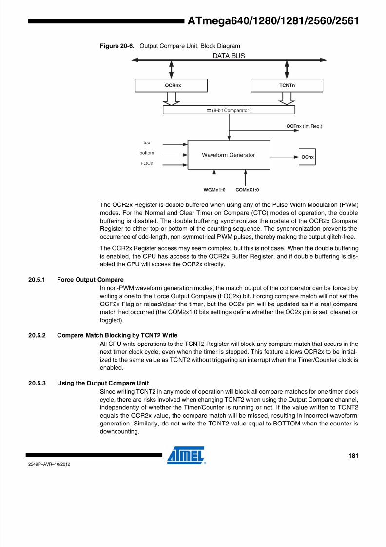
8/20/2019 At Mega 1281 Unlocked
http://slidepdf.com/reader/full/at-mega-1281-unlocked 181/446
181
2549P–AVR–10/2012
ATmega640/1280/1281/2560/2561
Figure 20-6. Output Compare Unit, Block Diagram
The OCR2x Register is double buffered when using any of the Pulse Width Modulation (PWM
modes. For the Normal and Clear Timer on Compare (CTC) modes of operation, the double
buffering is disabled. The double buffering synchronizes the update of the OCR2x Compare
Register to either top or bottom of the counting sequence. The synchronization prevents the
occurrence of odd-length, non-symmetrical PWM pulses, thereby making the output glitch-free.
The OCR2x Register access may seem complex, but this is not case. When the double buffering
is enabled, the CPU has access to the OCR2x Buffer Register, and if double buffering is dis-
abled the CPU will access the OCR2x directly.
20.5.1 Force Output CompareIn non-PWM waveform generation modes, the match output of the comparator can be forced by
writing a one to the Force Output Compare (FOC2x) bit. Forcing compare match will not set the
OCF2x Flag or reload/clear the timer, but the OC2x pin will be updated as if a real compare
match had occurred (the COM2x1:0 bits settings define whether the OC2x pin is set, cleared o
toggled).
20.5.2 Compare Match Blocking by TCNT2 Write
All CPU write operations to the TCNT2 Register will block any compare match that occurs in the
next timer clock cycle, even when the timer is stopped. This feature allows OCR2x to be initial-
ized to the same value as TCNT2 without triggering an interrupt when the Timer/Counter clock is
enabled.
20.5.3 Using the Output Compare Unit
Since writing TCNT2 in any mode of operation will block all compare matches for one timer clock
cycle, there are risks involved when changing TCNT2 when using the Output Compare channel
independently of whether the Timer/Counter is running or not. If the value written to TCNT2
equals the OCR2x value, the compare match will be missed, resulting in incorrect waveform
generation. Similarly, do not write the TCNT2 value equal to BOTTOM when the counter is
downcounting.
OCFnx (Int.Req.)
= (8-bit Comparator )
OCRnx
OCnx
DATA BUS
TCNTn
WGMn1:0
Waveform Generator
top
FOCn
COMnX1:0
bottom

8/20/2019 At Mega 1281 Unlocked
http://slidepdf.com/reader/full/at-mega-1281-unlocked 182/446
182
2549P–AVR–10/2012
ATmega640/1280/1281/2560/2561
The setup of the OC2x should be performed before setting the Data Direction Register for the
port pin to output. The easiest way of setting the OC2x value is to use the Force Output Com
pare (FOC2x) strobe bit in Normal mode. The OC2x Register keeps its value even when
changing between Waveform Generation modes.
Be aware that the COM2x1:0 bits are not double buffered together with the compare value.
Changing the COM2x1:0 bits will take effect immediately.
20.6 Compare Match Output Unit
The Compare Output mode (COM2x1:0) bits have two functions. The Waveform Generator uses
the COM2x1:0 bits for defining the Output Compare (OC2x) state at the next compare match
Also, the COM2x1:0 bits control the OC2x pin output source. Figure 20-7 shows a simplified
schematic of the logic affected by the COM2x1:0 bit setting. The I/O Registers, I/O bits, and I/O
pins in the figure are shown in bold. Only the parts of the general I/O Port Control Registers
(DDR and PORT) that are affected by the COM2x1:0 bits are shown. When referring to the
OC2x state, the reference is for the internal OC2x Register, not the OC2x pin.
Figure 20-7. Compare Match Output Unit, Schematic
The general I/O port function is overridden by the Output Compare (OC2x) from the Waveform
Generator if either of the COM2x1:0 bits are set. However, the OC2x pin direction (input or out-
put) is still controlled by the Data Direction Register (DDR) for the port pin. The Data DirectionRegister bit for the OC2x pin (DDR_OC2x) must be set as output before the OC2x value is visi-
ble on the pin. The port override function is independent of the Waveform Generation mode.
The design of the Output Compare pin logic allows initialization of the OC2x state before the out
put is enabled. Note that some COM2x1:0 bit settings are reserved for certain modes of
operation. See “Register Description” on page 187.
PORT
DDR
D Q
D Q
OCnx
PinOCnx
D QWaveform
Generator
COMnx1
COMnx0
0
1
DATA
BU
S
FOCnx
clkI/O

8/20/2019 At Mega 1281 Unlocked
http://slidepdf.com/reader/full/at-mega-1281-unlocked 183/446
183
2549P–AVR–10/2012
ATmega640/1280/1281/2560/2561
20.6.1 Compare Output Mode and Waveform Generation
The Waveform Generator uses the COM2x1:0 bits differently in normal, CTC, and PWM modes
For all modes, setting the COM2x1:0 = 0 tells the Waveform Generator that no action on the
OC2x Register is to be performed on the next compare match. For compare output actions in the
non-PWM modes refer to Table 20-5 on page 188. For fast PWM mode, refer to Table 20-6 on
page 188, and for phase correct PWM refer to Table 20-7 on page 189.
A change of the COM2x1:0 bits state will have effect at the first compare match after the bits are
written. For non-PWM modes, the action can be forced to have immediate effect by using the
FOC2x strobe bits.
20.7 Timer/Counter Timing Diagrams
The following figures show the Timer/Counter in synchronous mode, and the timer clock (clkT2
is therefore shown as a clock enable signal. In asynchronous mode, clkI/O should be replaced by
the Timer/Counter Oscillator clock. The figures include information on when Interrupt Flags are
set. Figure 20-8 contains timing data for basic Timer/Counter operation. The figure shows the
count sequence close to the MAX value in all modes other than phase correct PWM mode.
Figure 20-8. Timer/Counter Timing Diagram, no Prescaling
Figure 20-9 shows the same timing data, but with the prescaler enabled.
Figure 20-9. Timer/Counter Timing Diagram, with Prescaler (fclk_I/O /8)
clkTn
(clkI/O
/1)
TOVn
clkI/O
TCNTn MAX - 1 MAX BOTTOM BOTTOM + 1
TOVn
TCNTn MAX - 1 MAX BOTTOM BOTTOM + 1
clkI/O
clkTn
(clkI/O
/ 8)

8/20/2019 At Mega 1281 Unlocked
http://slidepdf.com/reader/full/at-mega-1281-unlocked 184/446
184
2549P–AVR–10/2012
ATmega640/1280/1281/2560/2561
Figure 20-10 shows the setting of OCF2A in all modes except CTC mode.
Figure 20-10. Timer/Counter Timing Diagram, Setting of OCF2A, with Prescaler (fclk_I/O /8)
Figure 20-11 shows the setting of OCF2A and the clearing of TCNT2 in CTC mode.
Figure 20-11. Timer/Counter Timing Diagram, Clear Timer on Compare Match mode, with Pres-caler (fclk_I/O /8)
20.8 Asynchronous Operation of Timer/Counter2
When Timer/Counter2 operates asynchronously, some considerations must be taken.
• Warning: When switching between asynchronous and synchronous clocking of
Timer/Counter2, the Timer Registers TCN
T2, OCR2x, and TCCR2x might be corrupted. Asafe procedure for switching clock source is:
1. Disable the Timer/Counter2 interrupts by clearing OCIE2x and TOIE2.
2. Select clock source by setting AS2 as appropriate.
3. Write new values to TCNT2, OCR2x, and TCCR2x.
4. To switch to asynchronous operation: Wait for TCN2UB, OCR2xUB, and TCR2xUB.
5. Clear the Timer/Counter2 Interrupt Flags.
6. Enable interrupts, if needed.
OCFnx
OCRnx
TCNTn
OCRnx Value
OCRnx - 1 OCRnx OCRnx + 1 OCRnx + 2
clkI/O
clkTn(clkI/O / 8)
OCFnx
OCRnx
TCNTn
(CTC)
TOP
TOP - 1 TOP BOTTOM BOTTOM + 1
clkI/O
clkTn
(clkI/O / 8)

8/20/2019 At Mega 1281 Unlocked
http://slidepdf.com/reader/full/at-mega-1281-unlocked 185/446
185
2549P–AVR–10/2012
ATmega640/1280/1281/2560/2561
• The CPU main clock frequency must be more than four times the Oscillator frequency.
• When writing to one of the registers TCNT2, OCR2x, or TCCR2x, the value is transferred toa temporary register, and latched after two positive edges on TOSC1. The user should notwrite a new value before the contents of the temporary register have been transferred to itsdestination. Each of the five mentioned registers have their individual temporary register,which means that, for example, writing to TCNT2 does not disturb an OCR2x write in
progress. To detect that a transfer to the destination register has taken place, theAsynchronous Status Register – ASSR has been implemented.
• When entering Power-save or ADC Noise Reduction mode after having written to TCNT2,OCR2x, or TCCR2x, the user must wait until the written register has been updated ifTimer/Counter2 is used to wake up the device. Otherwise, the MCU will enter sleep modebefore the changes are effective. This is particularly important if any of the OutputCompare2 interrupt is used to wake up the device, since the Output Compare function isdisabled during writing to OCR2x or TCNT2. If the write cycle is not finished, and the MCUenters sleep mode before the corresponding OCR2xUB bit returns to zero, the device willnever receive a compare match interrupt, and the MCU will not wake up.
• If Timer/Counter2 is used to wake the device up from Power-save or ADC Noise Reductionmode, precautions must be taken if the user wants to re-enter one of these modes: The
interrupt logic needs one TOSC1 cycle to be reset. If the time between wake-up and re-entering sleep mode is less than one TOSC1 cycle, the interrupt will not occur, and thedevice will fail to wake up. If the user is in doubt whether the time before re-entering Power-save or ADC Noise Reduction mode is sufficient, the following algorithm can be used toensure that one TOSC1 cycle has elapsed:
1. Write a value to TCCR2x, TCNT2, or OCR2x.
2. Wait until the corresponding Update Busy Flag in ASSR returns to zero.
3. Enter Power-save or ADC Noise Reduction mode.
• When the asynchronous operation is selected, the 32.768kHz Oscillator for Timer/Counter2is always running, except in Power-down and Standby modes. After a Power-up Reset orwake-up from Power-down or Standby mode, the user should be aware of the fact that thisOscillator might take as long as one second to stabilize. The user is advised to wait for at
least one second before using Timer/Counter2 after power-up or wake-up from Power-downor Standby mode. The contents of all Timer/Counter2 Registers must be considered lostafter a wake-up from Power-down or Standby mode due to unstable clock signal upon start-up, no matter whether the Oscillator is in use or a clock signal is applied to the TOSC1 pin.
• Description of wake up from Power-save or ADC Noise Reduction mode when the timer isclocked asynchronously: When the interrupt condition is met, the wake up process is startedon the following cycle of the timer clock, that is, the timer is always advanced by at least onebefore the processor can read the counter value. After wake-up, the MCU is halted for fourcycles, it executes the interrupt routine, and resumes execution from the instructionfollowing SLEEP.
• Reading of the TCNT2 Register shortly after wake-up from Power-save may give anincorrect result. Since TCNT2 is clocked on the asynchronous TOSC clock, reading TCNT2
must be done through a register synchronized to the internal I/O clock domain.Synchronization takes place for every rising TOSC1 edge. When waking up from Power-save mode, and the I/O clock (clkI/O) again becomes active, TCNT2 will read as the previousvalue (before entering sleep) until the next rising TOSC1 edge. The phase of the TOSCclock after waking up from Power-save mode is essentially unpredictable, as it depends onthe wake-up time. The recommended procedure for reading TCNT2 is thus as follows:
1. Write any value to either of the registers OCR2x or TCCR2x.
2. Wait for the corresponding Update Busy Flag to be cleared.
3. Read TCNT2.
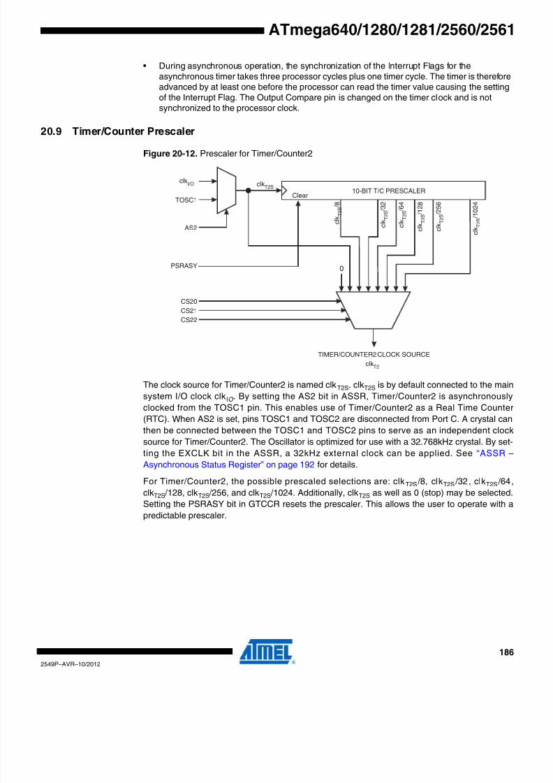
8/20/2019 At Mega 1281 Unlocked
http://slidepdf.com/reader/full/at-mega-1281-unlocked 186/446
186
2549P–AVR–10/2012
ATmega640/1280/1281/2560/2561
• During asynchronous operation, the synchronization of the Interrupt Flags for theasynchronous timer takes three processor cycles plus one timer cycle. The timer is thereforeadvanced by at least one before the processor can read the timer value causing the settingof the Interrupt Flag. The Output Compare pin is changed on the timer clock and is notsynchronized to the processor clock.
20.9 Timer/Counter Prescaler
Figure 20-12. Prescaler for Timer/Counter2
The clock source for Timer/Counter2 is named clkT2S. clkT2S is by default connected to the main
system I/O clock clkIO
. By setting the AS2 bit in ASSR, Timer/Counter2 is asynchronously
clocked from the TOSC1 pin. This enables use of Timer/Counter2 as a Real Time Counte
(RTC). When AS2 is set, pins TOSC1 and TOSC2 are disconnected from Port C. A crystal can
then be connected between the TOSC1 and TOSC2 pins to serve as an independent clock
source for Timer/Counter2. The Oscillator is optimized for use with a 32.768kHz crystal. By set
ting the EXCLK bit in the ASSR, a 32kHz external clock can be applied. See “ASSR –
Asynchronous Status Register” on page 192 for details.
For Timer/Counter2, the possible prescaled selections are: clkT2S /8, clkT2S /32, clkT2S /64
clkT2S /128, clkT2S /256, and clkT2S /1024. Additionally, clkT2S as well as 0 (stop) may be selected
Setting the PSRASY bit in GTCCR resets the prescaler. This allows the user to operate with a
predictable prescaler.
10-BIT T/C PRESCALER
TIMER/COUNTER2 CLOCK SOURCE
clkI/O clk
T2S
TOSC1
AS2
CS20
CS21
CS22
c l k
T2
S / 8
c l k
T2
S / 6 4
c l k
T2
S / 1 2 8
c l k
T2
S / 1 0 2 4
c l k
T2
S / 2 5 6
c l k
T2
S / 3 2
0PSRASY
Clear
clkT2

8/20/2019 At Mega 1281 Unlocked
http://slidepdf.com/reader/full/at-mega-1281-unlocked 187/446
187
2549P–AVR–10/2012
ATmega640/1280/1281/2560/2561
20.10 Register Description
20.10.1 TCCR2A –Timer/Counter Control Register A
• Bits 7:6 – COM2A1:0: Compare Match Output A Mode
These bits control the Output Compare pin (OC2A) behavior. If one or both of the COM2A1:0
bits are set, the OC2A output overrides the normal port functionality of the I/O pin it is connected
to. However, note that the Data Direction Register (DDR) bit corresponding to the OC2A pin
must be set in order to enable the output driver.
When OC2A is connected to the pin, the function of the COM2A1:0 bits depends on the
WGM22:0 bit setting. Table 20-2 shows the COM2A1:0 bit functionality when the WGM22:0 bits
are set to a normal or CTC mode (non-PWM).
Table 20-3 shows the COM2A1:0 bit functionality when the WGM21:0 bits are set to fast PWM
mode.
Note: 1. A special case occurs when OCR2A equals TOP and COM2A1 is set. In this case, the Com-pare Match is ignored, but the set or clear is done at BOTTOM. See “Fast PWM Mode” onpage 178 for more details.
Table 20-4 on page 188 shows the COM2A1:0 bit functionality when the WGM22:0 bits are se
to phase correct PWM mode.
Bit 7 6 5 4 3 2 1 0
(0xB0) COM2A1 COM2A0 COM2B1 COM2B0 – – WGM21 WGM20 TCCR2A
Read/ Write R/ W R/ W R/ W R/ W R R R/ W R/ W
Initial Value 0 0 0 0 0 0 0 0
Table 20-2. Compare Output Mode, non-PWM Mode
COM2A1 COM2A0 Description
0 0 Normal port operation, OC2A disconnected
0 1 Toggle OC2A on Compare Match
1 0 Clear OC2A on Compare Match
1 1 Set OC2A on Compare Match
Table 20-3. Compare Output Mode, Fast PWM Mode(1)
COM2A1 COM2A0 Description
0 0 Normal port operation, OC2A disconnected
0 1 WGM22 = 0: Normal Port Operation, OC2A Disconnected
WGM22 = 1: Toggle OC2A on Compare Match
1 0Clear OC2A on Compare Match, set OC2A at BOTTOM
(non-inverting mode)
1 1Set OC2A on Compare Match, clear OC2A at BOTTOM
(inverting mode)

8/20/2019 At Mega 1281 Unlocked
http://slidepdf.com/reader/full/at-mega-1281-unlocked 188/446
188
2549P–AVR–10/2012
ATmega640/1280/1281/2560/2561
Note: 1. A special case occurs when OCR2A equals TOP and COM2A1 is set. In this case, the Com-pare Match is ignored, but the set or clear is done at TOP. See “Phase Correct PWM Mode” onpage 179 for more details.
• Bits 5:4 – COM2B1:0: Compare Match Output B Mode
These bits control the Output Compare pin (OC2B) behavior. If one or both of the COM2B1:0
bits are set, the OC2B output overrides the normal port functionality of the I/O pin it is connected
to. However, note that the Data Direction Register (DDR) bit corresponding to the OC2B pin
must be set in order to enable the output driver.
When OC2B is connected to the pin, the function of the COM2B1:0 bits depends on the
WGM22:0 bit setting. Table 20-5 shows the COM2B1:0 bit functionality when the WGM22:0 bits
are set to a normal or CTC mode (non-PWM).
Table 20-6 shows the COM2B1:0 bit functionality when the WGM22:0 bits are set to fast PWM
mode.
Note: 1. A special case occurs when OCR2B equals TOP and COM2B1 is set. In this case, the Com-pare Match is ignored, but the set or clear is done at BOTTOM. See “Fast PWM Mode” onpage 178 for more details.
Table 20-4. Compare Output Mode, Phase Correct PWM Mode(1)
COM2A1 COM2A0 Description
0 0 Normal port operation, OC2A disconnected
0 1 WGM22 = 0: Normal Port Operation, OC2A Disconnected
WGM22 = 1: Toggle OC2A on Compare Match
1 0Clear OC2A on Compare Match when up-countingSet OC2A on Compare Match when down-counting
1 1Set OC2A on Compare Match when up-counting
Clear OC2A on Compare Match when down-counting
Table 20-5. Compare Output Mode, non-PWM Mode
COM2B1 COM2B0 Description
0 0 Normal port operation, OC2B disconnected
0 1 Toggle OC2B on Compare Match1 0 Clear OC2B on Compare Match
1 1 Set OC2B on Compare Match
Table 20-6. Compare Output Mode, Fast PWM Mode(1)
COM2B1 COM2B0 Description
0 0 Normal port operation, OC2B disconnected
0 1 Reserved
1 0 Clear OC2B on Compare Match, set OC2B at BOTTOM(non-inverting mode)
1 1Set OC2B on Compare Match, clear OC2B at BOTTOM
(inverting mode)
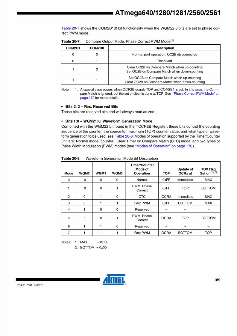
8/20/2019 At Mega 1281 Unlocked
http://slidepdf.com/reader/full/at-mega-1281-unlocked 189/446
189
2549P–AVR–10/2012
ATmega640/1280/1281/2560/2561
Table 20-7 shows the COM2B1:0 bit functionality when the WGM22:0 bits are set to phase cor-
rect PWM mode.
Note: 1. A special case occurs when OCR2B equals TOP and COM2B1 is set. In this case, the Com-pare Match is ignored, but the set or clear is done at TOP. See “Phase Correct PWM Mode” onpage 179 for more details.
• Bits 3, 2 – Res: Reserved Bits
These bits are reserved bits and will always read as zero.
• Bits 1:0 – WGM21:0: Waveform Generation Mode
Combined with the WGM22 bit found in the TCCR2B Register, these bits control the counting
sequence of the counter, the source for maximum (TOP) counter value, and what type of wave
form generation to be used, see Table 20-8. Modes of operation supported by the Timer/Counte
unit are: Normal mode (counter), Clear Timer on Compare Match (CTC) mode, and two types o
Pulse Width Modulation (PWM) modes (see “Modes of Operation” on page 176).
Notes: 1. MAX = 0xFF.
2. BOTTOM = 0x00.
Table 20-7. Compare Output Mode, Phase Correct PWM Mode(1)
COM2B1 COM2B0 Description
0 0 Normal port operation, OC2B disconnected
0 1 Reserved
1 0Clear OC2B on Compare Match when up-countingSet OC2B on Compare Match when down-counting
1 1Set OC2B on Compare Match when up-counting
Clear OC2B on Compare Match when down-counting
Table 20-8. Waveform Generation Mode Bit Description
Mode WGM2 WGM1 WGM0
Timer/Counter
Mode of
Operation TOP
Update of
OCRx at
TOV Flag
Set on(1)(2)
0 0 0 0 Normal 0xFF Immediate MAX
1 0 0 1PWM, Phase
Correct0xFF TOP BOTTOM
2 0 1 0 CTC OCRA Immediate MAX
3 0 1 1 Fast PWM 0xFF BOTTOM MAX
4 1 0 0 Reserved – – –
5 1 0 1PWM, Phase
CorrectOCRA TOP BOTTOM
6 1 1 0 Reserved – – –
7 1 1 1 Fast PWM OCRA BOTTOM TOP

8/20/2019 At Mega 1281 Unlocked
http://slidepdf.com/reader/full/at-mega-1281-unlocked 190/446
190
2549P–AVR–10/2012
ATmega640/1280/1281/2560/2561
20.10.2 TCCR2B – Timer/Counter Control Register B
• Bit 7 – FOC2A: Force Output Compare A
The FOC2A bit is only active when the WGM bits specify a non-PWM mode.
However, for ensuring compatibility with future devices, this bit must be set to zero when
TCCR2B is written when operating in PWM mode. When writing a logical one to the FOC2A bit
an immediate Compare Match is forced on the Waveform Generation unit. The OC2A output is
changed according to its COM2A1:0 bits setting. Note that the FOC2A bit is implemented as a
strobe. Therefore it is the value present in the COM2A1:0 bits that determines the effect of the
forced compare.
A FOC2A strobe will not generate any interrupt, nor will it clear the timer in CTC mode using
OCR2A as TOP.
The FOC2A bit is always read as zero.
• Bit 6 – FOC2B: Force Output Compare B
The FOC2B bit is only active when the WGM bits specify a non-PWM mode.
However, for ensuring compatibility with future devices, this bit must be set to zero when
TCCR2B is written when operating in PWM mode. When writing a logical one to the FOC2B bit
an immediate Compare Match is forced on the Waveform Generation unit. The OC2B output is
changed according to its COM2B1:0 bits setting. Note that the FOC2B bit is implemented as a
strobe. Therefore it is the value present in the COM2B1:0 bits that determines the effect of the
forced compare.
A FOC2B strobe will not generate any interrupt, nor will it clear the timer in CTC mode using
OCR2B as TOP.
The FOC2B bit is always read as zero.
• Bits 5:4 – Res: Reserved Bits
These bits are reserved bits and will always read as zero.
• Bit 3 – WGM22: Waveform Generation Mode
See the description in the “TCCR2A –Timer/Counter Control Register A” on page 187.
• Bit 2:0 – CS22:0: Clock Select
The three Clock Select bits select the clock source to be used by the Timer/Counter, see Table
20-9 on page 191.
Bit 7 6 5 4 3 2 1 0
(0xB1) FOC2A FOC2B – – WGM22 CS22 CS21 CS20 TCCR2B
Read/ Write W W R R R/ W R/ W R/ W R/ W
Initial Value 0 0 0 0 0 0 0 0

8/20/2019 At Mega 1281 Unlocked
http://slidepdf.com/reader/full/at-mega-1281-unlocked 191/446
191
2549P–AVR–10/2012
ATmega640/1280/1281/2560/2561
If external pin modes are used for the Timer/Counter0, transitions on the T0 pin will clock the
counter even if the pin is configured as an output. This feature allows software control of the
counting.
20.10.3 TCNT2 – Timer/Counter Register
The Timer/Counter Register gives direct access, both for read and write operations, to the
Timer/Counter unit 8-bit counter. Writing to the TCNT2 Register blocks (removes) the Compare
Match on the following timer clock. Modifying the counter (TCNT2) while the counter is running
introduces a risk of missing a Compare Match between TCNT2 and the OCR2x Registers.
20.10.4 OCR2A – Output Compare Register A
The Output Compare Register A contains an 8-bit value that is continuously compared with the
counter value (TCNT2). A match can be used to generate an Output Compare interrupt, or to
generate a waveform output on the OC2A pin.
20.10.5 OCR2B – Output Compare Register B
The Output Compare Register B contains an 8-bit value that is continuously compared with the
counter value (TCNT2). A match can be used to generate an Output Compare interrupt, or to
generate a waveform output on the OC2B pin.
Table 20-9. Clock Select Bit Description
CS22 CS21 CS20 Description
0 0 0 No clock source (Timer/Counter stopped)
0 0 1 clkT2S /(No prescaling)
0 1 0 clkT2S /8 (From prescaler)
0 1 1 clkT2S /32 (From prescaler)
1 0 0 clkT2S /64 (From prescaler)
1 0 1 clkT2S /128 (From prescaler)
1 1 0 clkT2S /256 (From prescaler)
1 1 1 clkT2S /1024 (From prescaler)
Bit 7 6 5 4 3 2 1 0
(0xB2) TCNT2[7:0] TCNT2
Read/ Write R/ W R/ W R/ W R/ W R/ W R/ W R/ W R/ W
Initial Value 0 0 0 0 0 0 0 0
Bit 7 6 5 4 3 2 1 0
(0xB3) OCR2A[7:0] OCR2A
Read/ Write R/ W R/ W R/ W R/ W R/ W R/ W R/ W R/ W
Initial Value 0 0 0 0 0 0 0 0
Bit 7 6 5 4 3 2 1 0
(0xB4) OCR2B[7:0] OCR2B
Read/ Write R/ W R/ W R/ W R/ W R/ W R/ W R/ W R/ W
Initial Value 0 0 0 0 0 0 0 0
8/20/2019 At Mega 1281 Unlocked
http://slidepdf.com/reader/full/at-mega-1281-unlocked 192/446
192
2549P–AVR–10/2012
ATmega640/1280/1281/2560/2561
20.10.6 ASSR – Asynchronous Status Register
• Bit 6 – EXCLK: Enable External Clock Input
When EXCLK is written to one, and asynchronous clock is selected, the external clock input buf
fer is enabled and an external clock can be input on Timer Oscillator 1 (TOSC1) pin instead of a
32kHz crystal. Writing to EXCLK should be done before asynchronous operation is selected
Note that the crystal Oscillator will only run when this bit is zero.
• Bit 5 – AS2: Asynchronous Timer/Counter2
When AS2 is written to zero, Timer/Counter2 is clocked from the I/O clock, clk I/O. When AS2 is
written to one, Timer/Counter2 is clocked from a crystal Oscillator connected to the Timer Oscil
lator 1 (TOSC1) pin. When the value of AS2 is changed, the contents of TCNT2, OCR2A,
OCR2B, TCCR2A and TCCR2B might be corrupted.
• Bit 4 – TCN2UB: Timer/Counter2 Update Busy
When Timer/Counter2 operates asynchronously and TCNT2 is written, this bit becomes set
When TCNT2 has been updated from the temporary storage register, this bit is cleared by hard
ware. A logical zero in this bit indicates that TCNT2 is ready to be updated with a new value.
• Bit 3 – OCR2AUB: Output Compare Register2 Update Busy
When Timer/Counter2 operates asynchronously and OCR2A is written, this bit becomes set.
When OCR2A has been updated from the temporary storage register, this bit is cleared by hard
ware. A logical zero in this bit indicates that OCR2A is ready to be updated with a new value.
• Bit 2 – OCR2BUB: Output Compare Register2 Update Busy
When Timer/Counter2 operates asynchronously and OCR2B is written, this bit becomes set.
When OCR2B has been updated from the temporary storage register, this bit is cleared by hard
ware. A logical zero in this bit indicates that OCR2B is ready to be updated with a new value.
• Bit 1 – TCR2AUB: Timer/Counter Control Register2 Update Busy
When Timer/Counter2 operates asynchronously and TCCR2A is written, this bit becomes set
When TCCR2A has been updated from the temporary storage register, this bit is cleared by
hardware. A logical zero in this bit indicates that TCCR2A is ready to be updated with a new
value.
• Bit 0 – TCR2BUB: Timer/Counter Control Register2 Update Busy
When Timer/Counter2 operates asynchronously and TCCR2B is written, this bit becomes set
When TCCR2B has been updated from the temporary storage register, this bit is cleared by
hardware. A logical zero in this bit indicates that TCCR2B is ready to be updated with a new
value.
If a write is performed to any of the five Timer/Counter2 Registers while its update busy flag is
set, the updated value might get corrupted and cause an unintentional interrupt to occur.
Bit 7 6 5 4 3 2 1 0
(0xB6) – EXCLK AS2 TCN2UB OCR2AUB OCR2BUB TCR2AUB TCR2BUB ASSR
Read/ Write R R/ W R/ W R R R R R
Initial Value 0 0 0 0 0 0 0 0

8/20/2019 At Mega 1281 Unlocked
http://slidepdf.com/reader/full/at-mega-1281-unlocked 193/446
193
2549P–AVR–10/2012
ATmega640/1280/1281/2560/2561
The mechanisms for reading TCNT2, OCR2A, OCR2B, TCCR2A and TCCR2B are different
When reading TCNT2, the actual timer value is read. When reading OCR2A, OCR2B, TCCR2A
and TCCR2B the value in the temporary storage register is read.
20.10.7 TIMSK2 – Timer/Counter2 Interrupt Mask Register
• Bit 2 – OCIE2B: Timer/Counter2 Output Compare Match B Interrupt Enable
When the OCIE2B bit is written to one and the I-bit in the Status Register is set (one), the
Timer/Counter2 Compare Match B interrupt is enabled. The corresponding interrupt is executed
if a compare match in Timer/Counter2 occurs, that is, when the OCF2B bit is set in the
Timer/Counter 2 Interrupt Flag Register – TIFR2.
• Bit 1 – OCIE2A: Timer/Counter2 Output Compare Match A Interrupt Enable
When the OCIE2A bit is written to one and the I-bit in the Status Register is set (one), the
Timer/Counter2 Compare Match A interrupt is enabled. The corresponding interrupt is executedif a compare match in Timer/Counter2 occurs, that is, when the OCF2A bit is set in the
Timer/Counter 2 Interrupt Flag Register – TIFR2.
• Bit 0 – TOIE2: Timer/Counter2 Overflow Interrupt Enable
When the TOIE2 bit is written to one and the I-bit in the Status Register is set (one), the
Timer/Counter2 Overflow interrupt is enabled. The corresponding interrupt is executed if an
overflow in Timer/Counter2 occurs, that is, when the TOV2 bit is set in the Timer/Counter2 Inter
rupt Flag Register – TIFR2.
20.10.8 TIFR2 – Timer/Counter2 Interrupt Flag Register
• Bit 2 – OCF2B: Output Compare Flag 2 B
The OCF2B bit is set (one) when a compare match occurs between the Timer/Counter2 and the
data in OCR2B – Output Compare Register2. OCF2B is cleared by hardware when executing
the corresponding interrupt handling vector. Alternatively, OCF2B is cleared by writing a logic
one to the flag. When the I-bit in SREG, OCIE2B (Timer/Counter2 Compare match Interrupt
Enable), and OCF2B are set (one), the Timer/Counter2 Compare match Interrupt is executed.
• Bit 1 – OCF2A: Output Compare Flag 2 A
The OCF2A bit is set (one) when a compare match occurs between the Timer/Counter2 and the
data in OCR2A – Output Compare Register2. OCF2A is cleared by hardware when executing
the corresponding interrupt handling vector. Alternatively, OCF2A is cleared by writing a logic
one to the flag. When the I-bit in SREG, OCIE2A (Timer/Counter2 Compare match Interrupt
Enable), and OCF2A are set (one), the Timer/Counter2 Compare match Interrupt is executed.
Bit 7 6 5 4 3 2 1 0
(0x70) – – – – – OCIE2B OCIE2A TOIE2 TIMSK2
Read/ Write R R R R R R/ W R/ W R/ W
Initial Value 0 0 0 0 0 0 0 0
Bit 7 6 5 4 3 2 1 0
0x17 (0x37) – – – – – OCF2B OCF2A TOV2 TIFR2
Read/ Write R R R R R R/ W R/ W R/ W
Initial Value 0 0 0 0 0 0 0 0
8/20/2019 At Mega 1281 Unlocked
http://slidepdf.com/reader/full/at-mega-1281-unlocked 194/446
194
2549P–AVR–10/2012
ATmega640/1280/1281/2560/2561
• Bit 0 – TOV2: Timer/Counter2 Overflow Flag
The TOV2 bit is set (one) when an overflow occurs in Timer/Counter2. TOV2 is cleared by hard-
ware when executing the corresponding interrupt handling vector. Alternatively, TOV2 is cleared
by writing a logic one to the flag. When the SREG I-bit, TOIE2A (Timer/Counter2 Overflow Inter
rupt Enable), and TOV2 are set (one), the Timer/Counter2 Overflow interrupt is executed. InPWM mode, this bit is set when Timer/Counter2 changes counting direction at 0x00.
20.10.9 GTCCR – General Timer/Counter Control Register
• Bit 1 – PSRASY: Prescaler Reset Timer/Counter2
When this bit is one, the Timer/Counter2 prescaler will be reset. This bit is normally cleared
immediately by hardware. If the bit is written when Timer/Counter2 is operating in asynchronous
mode, the bit will remain one until the prescaler has been reset. The bit will not be cleared byhardware if the TSM bit is set. Refer to the description of the “Bit 7 – TSM: Timer/Counter Syn
chronization Mode” on page 170 for a description of the Timer/Counter Synchronization mode.
Bit 7 6 5 4 3 2 1 0
0x23 (0x43) TSM – – – – – PSRASY PSRSYNC GTCCR
Read/ Write R/ W R R R R R R/ W R/ W
Initial Value 0 0 0 0 0 0 0 0

8/20/2019 At Mega 1281 Unlocked
http://slidepdf.com/reader/full/at-mega-1281-unlocked 195/446
195
2549P–AVR–10/2012
ATmega640/1280/1281/2560/2561
21. SPI – Serial Peripheral InterfaceThe Serial Peripheral Interface (SPI) allows high-speed synchronous data transfer between the
ATmega640/1280/1281/2560/2561 and peripheral devices or between several AVR devices
The ATmega640/1280/1281/2560/2561 SPI includes the following features:
• Full-duplex, Three-wire Synchronous Data Transfer
• Master or Slave Operation• LSB First or MSB First Data Transfer
• Seven Programmable Bit Rates
• End of Transmission Interrupt Flag
• Write Collision Flag Protection
• Wake-up from Idle Mode
• Double Speed (CK/2) Master SPI Mode
USART can also be used in Master SPI mode, see “USART in SPI Mode” on page 232.
The Power Reduction SPI bit, PRSPI, in “PRR0 – Power Reduction Register 0” on page 56 on
page 50 must be written to zero to enable SPI module.
Figure 21-1. SPI Block Diagram(1)
Note: 1. Refer to Figure 1-1 on page 2, and Table 13-6 on page 79 for SPI pin placement.
The interconnection between Master and Slave CPUs with SPI is shown in Figure 21-2 on page
196. The system consists of two shift Registers, and a Master clock generator. The SPI Master
initiates the communication cycle when pulling low the Slave Select SS pin of the desired Slave
S P I 2 X
S P I 2 X
DIVIDER
/2/4/ 8 /16/32/64/128

8/20/2019 At Mega 1281 Unlocked
http://slidepdf.com/reader/full/at-mega-1281-unlocked 196/446
196
2549P–AVR–10/2012
ATmega640/1280/1281/2560/2561
Master and Slave prepare the data to be sent in their respective shift Registers, and the Maste
generates the required clock pulses on the SCK line to interchange data. Data is always shifted
from Master to Slave on the Master Out – Slave In, MOSI, line, and from Slave to Master on the
Master In – Slave Out, MISO, line. After each data packet, the Master will synchronize the Slave
by pulling high the Slave Select, SS, line.
When configured as a Master, the SPI interface has no automatic control of the SS line. This
must be handled by user software before communication can start. When this is done, writing a
byte to the SPI Data Register starts the SPI clock generator, and the hardware shifts the eight
bits into the Slave. After shifting one byte, the SPI clock generator stops, setting the end of
Transmission Flag (SPIF). If the SPI Interrupt Enable bit (SPIE) in the SPCR Register is set, an
interrupt is requested. The Master may continue to shift the next byte by writing it into SPDR, or
signal the end of packet by pulling high the Slave Select, SS line. The last incoming byte will be
kept in the Buffer Register for later use.
When configured as a Slave, the SPI interface will remain sleeping with MISO tri-stated as long
as the SS pin is driven high. In this state, software may update the contents of the SPI Data
Register, SPDR, but the data will not be shifted out by incoming clock pulses on the SCK pin
until the SS pin is driven low. As one byte has been completely shifted, the end of Transmission
Flag, SPIF is set. If the SPI Interrupt Enable bit, SPIE, in the SPCR Register is set, an interruptis requested. The Slave may continue to place new data to be sent into SPDR before reading
the incoming data. The last incoming byte will be kept in the Buffer Register for later use.
Figure 21-2. SPI Master-slave Interconnection
The system is single buffered in the transmit direction and double buffered in the receive direc-
tion. This means that bytes to be transmitted cannot be written to the SPI Data Register before
the entire shift cycle is completed. When receiving data, however, a received character must be
read from the SPI Data Register before the next character has been completely shifted in. Oth-
erwise, the first byte is lost.
In SPI Slave mode, the control logic will sample the incoming signal of the SCK pin. To ensure
correct sampling of the clock signal, the minimum low and high periods should be:
Low period: longer than 2 CPU clock cycles.
High period: longer than 2 CPU clock cycles.
When the SPI is enabled, the data direction of the MOSI, MISO, SCK, and SS pins is overridden
according to Table 21-1. For more details on automatic port overrides, refer to “Alternate Por
SHIFTENABLE

8/20/2019 At Mega 1281 Unlocked
http://slidepdf.com/reader/full/at-mega-1281-unlocked 197/446
197
2549P–AVR–10/2012
ATmega640/1280/1281/2560/2561
Functions” on page 75.
Note: 1. See “Alternate Functions of Port B” on page 79 for a detailed description of how to define thedirection of the user defined SPI pins.
The following code examples show how to initialize the SPI as a Master and how to perform a
simple transmission. DDR_SPI in the examples must be replaced by the actual Data Direction
Register controlling the SPI pins. DD_MOSI, DD_MISO and DD_SCK must be replaced by the
actual data direction bits for these pins. For example, if MOSI is placed on pin PB5, replace
DD_MOSI with DDB5 and DDR_SPI with DDRB.
Table 21-1. SPI Pin Overrides(1)
Pin Direction, Master SPI Direction, Slave SPI
MOSI User Defined Input
MISO Input User Defined
SCK User Defined Input
SS User Defined Input

8/20/2019 At Mega 1281 Unlocked
http://slidepdf.com/reader/full/at-mega-1281-unlocked 198/446
198
2549P–AVR–10/2012
ATmega640/1280/1281/2560/2561
Note: 1. See “About Code Examples” on page 11.
Assembly Code Example(1)
SPI_MasterInit:
; Set MOSI and SCK output, all others input
ldi r17,(1<<DD_MOSI)|(1<<DD_SCK)
out DDR_SPI,r17; Enable SPI, Master, set clock rate fck/16
ldi r17,(1<<SPE)|(1<<MSTR)|(1<<SPR0)
out SPCR,r17
ret
SPI_MasterTransmit:
; Start transmission of data (r16)
out SPDR,r16
Wait_Transmit:
; Wait for transmission complete
sbis SPSR,SPIF
rjmp Wait_Transmit
ret
C Code Example(1)
void SPI_MasterInit( void)
{
/* Set MOSI and SCK output, all others input */
DDR_SPI = (1<<DD_MOSI)|(1<<DD_SCK);
/* Enable SPI, Master, set clock rate fck/16 */
SPCR = (1<<SPE)|(1<<MSTR)|(1<<SPR0);
}
void SPI_MasterTransmit(char cData)
{
/* Start transmission */
SPDR = cData;
/* Wait for transmission complete */
while(!(SPSR & (1<<SPIF)))
;
}

8/20/2019 At Mega 1281 Unlocked
http://slidepdf.com/reader/full/at-mega-1281-unlocked 199/446
199
2549P–AVR–10/2012
ATmega640/1280/1281/2560/2561
The following code examples show how to initialize the SPI as a Slave and how to perform a
simple reception.
Note: 1. See “About Code Examples” on page 11.
Assembly Code Example(1)
SPI_SlaveInit:
; Set MISO output, all others input
ldi r17,(1<<DD_MISO)
out DDR_SPI,r17
; Enable SPI
ldi r17,(1<<SPE)
out SPCR,r17
ret
SPI_SlaveReceive:
; Wait for reception complete
sbis SPSR,SPIF
rjmp SPI_SlaveReceive
; Read received data and return
in r16,SPDR
ret
C Code Example(1)
void SPI_SlaveInit( void)
{
/* Set MISO output, all others input */
DDR_SPI = (1<<DD_MISO);
/* Enable SPI */
SPCR = (1<<SPE);
}
char SPI_SlaveReceive( void)
{
/* Wait for reception complete */
while(!(SPSR & (1<<SPIF)))
;
/* Return Data Register */
return SPDR;
}

8/20/2019 At Mega 1281 Unlocked
http://slidepdf.com/reader/full/at-mega-1281-unlocked 200/446
200
2549P–AVR–10/2012
ATmega640/1280/1281/2560/2561
21.1 SS Pin Functionality
21.1.1 Slave Mode
When the SPI is configured as a Slave, the Slave Select (SS) pin is always input. When SS is
held low, the SPI is activated, and MISO becomes an output if configured so by the user. Al
other pins are inputs. When SS is driven high, all pins are inputs, and the SPI is passive, which
means that it will not receive incoming data. Note that the SPI logic will be reset once the SS pinis driven high.
The SS pin is useful for packet/byte synchronization to keep the slave bit counter synchronous
with the master clock generator. When the SS pin is driven high, the SPI slave will immediately
reset the send and receive logic, and drop any partially received data in the Shift Register.
21.1.2 Master Mode
When the SPI is configured as a Master (MSTR in SPCR is set), the user can determine the
direction of the SS pin.
If SS is configured as an output, the pin is a general output pin which does not affect the SP
system. Typically, the pin will be driving the SS pin of the SPI Slave.
If SS is configured as an input, it must be held high to ensure Master SPI operation. If the SS pin
is driven low by peripheral circuitry when the SPI is configured as a Master with the SS pin
defined as an input, the SPI system interprets this as another master selecting the SPI as a
slave and starting to send data to it. To avoid bus contention, the SPI system takes the following
actions:
1. The MSTR bit in SPCR is cleared and the SPI system becomes a Slave. As a result ofthe SPI becoming a Slave, the MOSI and SCK pins become inputs.
2. The SPIF Flag in SPSR is set, and if the SPI interrupt is enabled, and the I-bit in SREG isset, the interrupt routine will be executed.
Thus, when interrupt-driven SPI transmission is used in Master mode, and there exists a possi-
bility that SS is driven low, the interrupt should always check that the MSTR bit is still set. If theMSTR bit has been cleared by a slave select, it must be set by the user to re-enable SPI Maste
mode.
21.1.3 Data Modes
There are four combinations of SCK phase and polarity with respect to serial data, which are
determined by control bits CPHA and CPOL. The SPI data transfer formats are shown in Figure
21-3 on page 201 and Figure 21-4 on page 201. Data bits are shifted out and latched in on
opposite edges of the SCK signal, ensuring sufficient time for data signals to stabilize. This is
clearly seen by summarizing Table 21-3 on page 202 and Table 21-4 on page 202 in Table 21-2
Table 21-2. CPOL Functionality
Leading Edge Trailing eDge SPI Mode
CPOL=0, CPHA=0 Sample (Rising) Setup (Falling) 0
CPOL=0, CPHA=1 Setup (Rising) Sample (Falling) 1
CPOL=1, CPHA=0 Sample (Falling) Setup (Rising) 2
CPOL=1, CPHA=1 Setup (Falling) Sample (Rising) 3

8/20/2019 At Mega 1281 Unlocked
http://slidepdf.com/reader/full/at-mega-1281-unlocked 201/446
201
2549P–AVR–10/2012
ATmega640/1280/1281/2560/2561
Figure 21-3. SPI Transfer Format with CPHA = 0
Figure 21-4. SPI Transfer Format with CPHA = 1
Bit 1Bit 6
LSBMSB
SCK (CPOL = 0)
mode 0
SAMPLE IMOSI/MISO
CHANGE 0
MOSI PIN
CHANGE 0
MISO PIN
SCK (CPOL = 1)
mode 2
SS
MSBLSB
Bit 6Bit 1
Bit 5Bit 2
Bit 4Bit 3
Bit 3Bit 4
Bit 2Bit 5
MSB first (DORD = 0)LSB first (DORD = 1)
SCK (CPOL = 0)
mode 1
SAMPLE I
MOSI/MISO
CHANGE 0
MOSI PIN
CHANGE 0
MISO PIN
SCK (CPOL = 1)
mode 3
SS
MSBLSB
Bit 6Bit 1
Bit 5Bit 2
Bit 4Bit 3
Bit 3Bit 4
Bit 2Bit 5
Bit 1Bit 6
LSBMSB
MSB first (DORD = 0)LSB first (DORD = 1)

8/20/2019 At Mega 1281 Unlocked
http://slidepdf.com/reader/full/at-mega-1281-unlocked 202/446
202
2549P–AVR–10/2012
ATmega640/1280/1281/2560/2561
21.2 Register Description
21.2.1 SPCR – SPI Control Register
• Bit 7 – SPIE: SPI Interrupt Enable
This bit causes the SPI interrupt to be executed if SPIF bit in the SPSR Register is set and the i
the Global Interrupt Enable bit in SREG is set.
• Bit 6 – SPE: SPI Enable
When the SPE bit is written to one, the SPI is enabled. This bit must be set to enable any SP
operations.
• Bit 5 – DORD: Data Order
When the DORD bit is written to one, the LSB of the data word is transmitted first.
When the DORD bit is written to zero, the MSB of the data word is transmitted first.
• Bit 4 – MSTR: Master/Slave Select
This bit selects Master SPI mode when written to one, and Slave SPI mode when written logic
zero. If SS is configured as an input and is driven low while MSTR is set, MSTR will be cleared
and SPIF in SPSR will become set. The user will then have to set MSTR to re-enable SPI Mas-
ter mode.
• Bit 3 – CPOL: Clock Polarity
When this bit is written to one, SCK is high when idle. When CPOL is written to zero, SCK is lowwhen idle. Refer to Figure 21-3 on page 201 and Figure 21-4 on page 201 for an example. The
CPOL functionality is summarized in Table 21-3.
• Bit 2 – CPHA: Clock Phase
The settings of the Clock Phase bit (CPHA) determine if data is sampled on the leading (first) or
trailing (last) edge of SCK. Refer to Figure 21-3 on page 201 and Figure 21-4 on page 201 for anexample. The CPOL functionality is summarized in Table 21-4.
Bit 7 6 5 4 3 2 1 0
0x2C (0x4C) SPIE SPE DORD MSTR CPOL CPHA SPR1 SPR0 SPCR
Read/ Write R/ W R/ W R/ W R/ W R/ W R/ W R/ W R/ W
Initial Value 0 0 0 0 0 0 0 0
Table 21-3. CPOL Functionality
CPOL Leading Edge Trailing Edge
0 Rising Falling
1 Falling Rising
Table 21-4. CPHA Functionality
CPHA Leading Edge Trailing Edge
0 Sample Setup
1 Setup Sample

8/20/2019 At Mega 1281 Unlocked
http://slidepdf.com/reader/full/at-mega-1281-unlocked 203/446
203
2549P–AVR–10/2012
ATmega640/1280/1281/2560/2561
• Bits 1, 0 – SPR1, SPR0: SPI Clock Rate Select 1 and 0
These two bits control the SCK rate of the device configured as a Master. SPR1 and SPR0 have
no effect on the Slave. The relationship between SCK and the Oscillator Clock frequency fosc is
shown in Table 21-5.
21.2.2 SPSR – SPI Status Register
• Bit 7 – SPIF: SPI Interrupt Flag
When a serial transfer is complete, the SPIF Flag is set. An interrupt is generated if SPIE in
SPCR is set and global interrupts are enabled. If SS is an input and is driven low when the SPI is
in Master mode, this will also set the SPIF Flag. SPIF is cleared by hardware when executing the
corresponding interrupt handling vector. Alternatively, the SPIF bit is cleared by first reading the
SPI Status Register with SPIF set, then accessing the SPI Data Register (SPDR).
• Bit 6 – WCOL: Write COLlision Flag
The WCOL bit is set if the SPI Data Register (SPDR) is written during a data transfer. The
WCOL bit (and the SPIF bit) are cleared by first reading the SPI Status Register with WCOL set
and then accessing the SPI Data Register.
• Bit 5:1 – Res: Reserved Bits
These bits are reserved bits and will always read as zero.
• Bit 0 – SPI2X: Double SPI Speed Bit
When this bit is written logic one the SPI speed (SCK Frequency) will be doubled when the SPI
is in Master mode (see Table 21-5). This means that the minimum SCK period will be two CPUclock periods. When the SPI is configured as Slave, the SPI is only guaranteed to work at fosc /4
or lower.
The SPI interface on the ATmega640/1280/1281/2560/2561 is also used for program memory
and EEPROM downloading or uploading. See “Serial Downloading” on page 349 for serial pro
gramming and verification.
Table 21-5. Relationship Between SCK and the Oscillator Frequency
SPI2X SPR1 SPR0 SCK Frequency
0 0 0 fosc / 4
0 0 1 fosc / 16
0 1 0 fosc / 64
0 1 1 fosc / 128
1 0 0 fosc / 2
1 0 1 fosc / 8
1 1 0 fosc / 32
1 1 1 fosc / 64
Bit 7 6 5 4 3 2 1 0
0x2D (0x4D) SPIF WCOL – – – – – SPI2X SPSR
Read/ Write R R R R R R R R/ W
Initial Value 0 0 0 0 0 0 0 0
8/20/2019 At Mega 1281 Unlocked
http://slidepdf.com/reader/full/at-mega-1281-unlocked 204/446
204
2549P–AVR–10/2012
ATmega640/1280/1281/2560/2561
21.2.3 SPDR – SPI Data Register
The SPI Data Register is a read/write register used for data transfer between the Register File
and the SPI Shift Register. Writing to the register initiates data transmission. Reading the regis
ter causes the Shift Register Receive buffer to be read.
Bit 7 6 5 4 3 2 1 0
0x2E (0x4E) MSB LSB SPDR
Read/ Write R/ W R/ W R/ W R/ W R/ W R/ W R/ W R/ W
Initial Value X X X X X X X X Undefined

8/20/2019 At Mega 1281 Unlocked
http://slidepdf.com/reader/full/at-mega-1281-unlocked 205/446
205
2549P–AVR–10/2012
ATmega640/1280/1281/2560/2561
22. USART
22.1 Features• Full Duplex Operation (Independent Serial Receive and Transmit Registers)
• Asynchronous or Synchronous Operation
• Master or Slave Clocked Synchronous Operation
• High Resolution Baud Rate Generator
• Supports Serial Frames with 5, 6, 7, 8, or 9 Data Bits and 1 or 2 Stop Bits
• Odd or Even Parity Generation and Parity Check Supported by Hardware
• Data OverRun Detection
• Framing Error Detection
• Noise Filtering Includes False Start Bit Detection and Digital Low Pass Filter
• Three Separate Interrupts on TX Complete, TX Data Register Empty and RX Complete
• Multi-processor Communication Mode
• Double Speed Asynchronous Communication Mode
Overview The Universal Synchronous and Asynchronous serial Receiver and Transmitter (USART) is a
highly flexible serial communication device.
The ATmega640/1280/2560 has four USART’s, USART0, USART1, USART2, and USART3
The functionality for all four USART’s is described below. USART0, USART1, USART2, and
USART3 have different I/O registers as shown in “Register Summary” on page 411.
A simplified block diagram of the USART Transmitter is shown in Figure 22-1 on page 206. CPU
accessible I/O Registers and I/O pins are shown in bold.
The Power Reducion USART0 bit, PRUSART0, in “PRR0 – Power Reduction Register 0” on
page 56 must be disabled by writing a logical zero to it.
The Power Reducion USART1 bit, PRUSART1, in “PRR1 – Power Reduction Register 1” on
page 57 must be disabled by writing a logical zero to it.
The Power Reducion USART2 bit, PRUSART2, in “PRR1 – Power Reduction Register 1” on
page 57 must be disabled by writing a logical zero to it.
The Power Reducion USART3 bit, PRUSART3, in “PRR1 – Power Reduction Register 1” on
page 57 must be disabled by writing a logical zero to it.

8/20/2019 At Mega 1281 Unlocked
http://slidepdf.com/reader/full/at-mega-1281-unlocked 206/446
206
2549P–AVR–10/2012
ATmega640/1280/1281/2560/2561
Figure 22-1. USART Block Diagram(1)
Note: 1. See Figure 1-1 on page 2, Figure 1-3 on page 4, Table 13-12 on page 83, Table 13-15 onpage 86, Table 13-24 on page 92 and Table 13-27 on page 94 for USART pin placement.
The dashed boxes in the block diagram separate the three main parts of the USART (listed from
the top): Clock Generator, Transmitter and Receiver. Control Registers are shared by all units
The Clock Generation logic consists of synchronization logic for external clock input used by
synchronous slave operation, and the baud rate generator. The XCKn (Transfer Clock) pin is
only used by synchronous transfer mode. The Transmitter consists of a single write buffer, a
serial Shift Register, Parity Generator and Control logic for handling different serial frame for
mats. The write buffer allows a continuous transfer of data without any delay between frames.
The Receiver is the most complex part of the USART module due to its clock and data recovery
units. The recovery units are used for asynchronous data reception. In addition to the recovery
units, the Receiver includes a Parity Checker, Control logic, a Shift Register and a two leve
receive buffer (UDRn). The Receiver supports the same frame formats as the Transmitter, and
can detect Frame Error, Data OverRun and Parity Errors.
22.2 Clock Generation
The Clock Generation logic generates the base clock for the Transmitter and Receiver. The
USARTn supports four modes of clock operation: Normal asynchronous, Double Speed asyn
chronous, Master synchronous and Slave synchronous mode. The UMSELn bit in USART
Control and Status Register C (UCSRnC) selects between asynchronous and synchronous
operation. Double Speed (asynchronous mode only) is controlled by the U2Xn found in the
PARITYGENERATOR
UBRR[H:L]
UDR (Transmit)
UCSRA UCSRB UCSRC
BAUD RATE GENERATOR
TRANSMIT SHIFT REGISTER
RECEIVE SHIFT REGISTER RxD
TxDPIN
CONTROL
UDR (Receive)
PINCONTROL
XCK
DATARECOVERY
CLOCK
RECOVERY
PIN
CONTROL
TXCONTROL
RX
CONTROL
PARITYCHECKER
D A T A
B U S
OSC
SYNC LOGIC
Clock Generator
Transmitter
Receiver

8/20/2019 At Mega 1281 Unlocked
http://slidepdf.com/reader/full/at-mega-1281-unlocked 207/446
207
2549P–AVR–10/2012
ATmega640/1280/1281/2560/2561
UCSRnA Register. When using synchronous mode (UMSELn = 1), the Data Direction Register
for the XCKn pin (DDR_XCKn) controls whether the clock source is internal (Master mode) or
external (Slave mode). The XCKn pin is only active when using synchronous mode.
Figure 22-2 shows a block diagram of the clock generation logic.
Figure 22-2. Clock Generation Logic, Block Diagram
Signal description:
txclk Transmitter clock (Internal Signal).
rxclk Receiver base clock (Internal Signal).
xcki Input from XCK pin (internal Signal). Used for synchronous slave
operation.
xcko Clock output to XCK pin (Internal Signal). Used for synchronous maste
operation.
fOSC
XTAL pin frequency (System Clock).
22.2.1 Internal Clock Generation – The Baud Rate Generator
Internal clock generation is used for the asynchronous and the synchronous master modes of
operation. The description in this section refers to Figure 22-2.
The USART Baud Rate Register (UBRRn) and the down-counter connected to it function as a
programmable prescaler or baud rate generator. The down-counter, running at system clock
(fosc), is loaded with the UBRRn value each time the counter has counted down to zero or when
the UBRRLn Register is written. A clock is generated each time the counter reaches zero. This
clock is the baud rate generator clock output (= fosc /(UBRRn+1)). The Transmitter divides the
baud rate generator clock output by 2, 8 or 16 depending on mode. The baud rate generator out
put is used directly by the Receiver’s clock and data recovery units. However, the recovery units
use a state machine that uses 2, 8 or 16 states depending on mode set by the state of theUMSELn, U2Xn and DDR_XCKn bits.
Table 22-1 on page 208 contains equations for calculating the baud rate (in bits per second) and
for calculating the UBRRn value for each mode of operation using an internally generated clock
source.
PrescalingDown-Counter
/2
UBRR
/4 /2
fosc
UBRR+1
SyncRegister
OSC
XCKPin
txclk
U2X
UMSEL
DDR_XCK
0
1
0
1
xcki
xcko
DDR_XCKrxclk
0
1
1
0
EdgeDetector
UCPOL
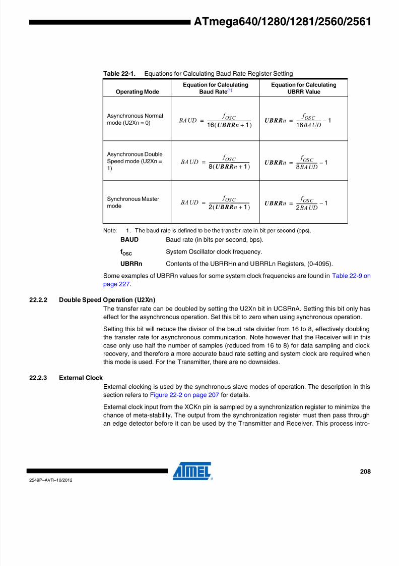
8/20/2019 At Mega 1281 Unlocked
http://slidepdf.com/reader/full/at-mega-1281-unlocked 208/446
208
2549P–AVR–10/2012
ATmega640/1280/1281/2560/2561
Note: 1. The baud rate is defined to be the transfer rate in bit per second (bps).
BAUD Baud rate (in bits per second, bps).
fOSC System Oscillator clock frequency.
UBRRn Contents of the UBRRHn and UBRRLn Registers, (0-4095).
Some examples of UBRRn values for some system clock frequencies are found in Table 22-9 on
page 227.
22.2.2 Double Speed Operation (U2Xn)
The transfer rate can be doubled by setting the U2Xn bit in UCSRnA. Setting this bit only has
effect for the asynchronous operation. Set this bit to zero when using synchronous operation.
Setting this bit will reduce the divisor of the baud rate divider from 16 to 8, effectively doubling
the transfer rate for asynchronous communication. Note however that the Receiver will in this
case only use half the number of samples (reduced from 16 to 8) for data sampling and clock
recovery, and therefore a more accurate baud rate setting and system clock are required when
this mode is used. For the Transmitter, there are no downsides.
22.2.3 External Clock
External clocking is used by the synchronous slave modes of operation. The description in thissection refers to Figure 22-2 on page 207 for details.
External clock input from the XCKn pin is sampled by a synchronization register to minimize the
chance of meta-stability. The output from the synchronization register must then pass through
an edge detector before it can be used by the Transmitter and Receiver. This process intro-
Table 22-1. Equations for Calculating Baud Rate Register Setting
Operating Mode
Equation for Calculating
Baud Rate(1)Equation for Calculating
UBRR Value
Asynchronous Normalmode (U2Xn = 0)
Asynchronous DoubleSpeed mode (U2Xn =1)
Synchronous Mastermode
BA UD f OS C
16 UBRRn 1+( )------------------------------------------= UBRRn
f OS C
16 BA UD------------------------ 1–=
BA UD f OS C
8 UBRRn 1+( )---------------------------------------= UBRRn
f OS C
8 BA UD-------------------- 1–=
BA UD f OS C
2 UBRRn 1+( )---------------------------------------= UBRRn
f OS C
2 BA UD-------------------- 1–=
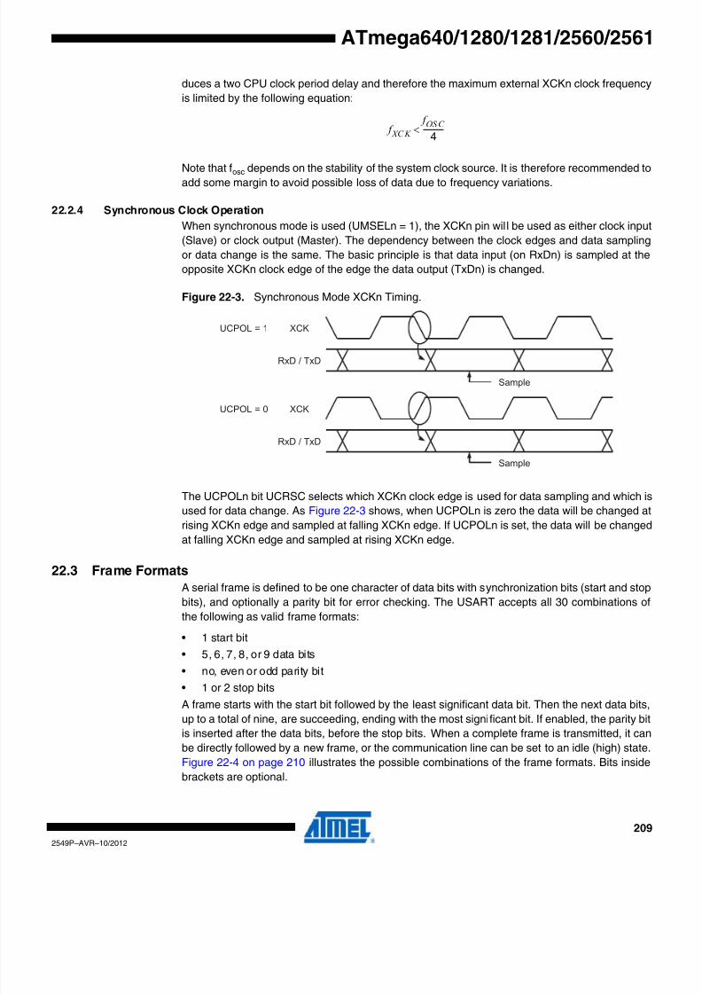
8/20/2019 At Mega 1281 Unlocked
http://slidepdf.com/reader/full/at-mega-1281-unlocked 209/446
209
2549P–AVR–10/2012
ATmega640/1280/1281/2560/2561
duces a two CPU clock period delay and therefore the maximum external XCKn clock frequency
is limited by the following equation:
Note that fosc depends on the stability of the system clock source. It is therefore recommended toadd some margin to avoid possible loss of data due to frequency variations.
22.2.4 Synchronous Clock Operation
When synchronous mode is used (UMSELn = 1), the XCKn pin will be used as either clock inpu
(Slave) or clock output (Master). The dependency between the clock edges and data sampling
or data change is the same. The basic principle is that data input (on RxDn) is sampled at the
opposite XCKn clock edge of the edge the data output (TxDn) is changed.
Figure 22-3. Synchronous Mode XCKn Timing.
The UCPOLn bit UCRSC selects which XCKn clock edge is used for data sampling and which is
used for data change. As Figure 22-3 shows, when UCPOLn is zero the data will be changed atrising XCKn edge and sampled at falling XCKn edge. If UCPOLn is set, the data will be changed
at falling XCKn edge and sampled at rising XCKn edge.
22.3 Frame Formats
A serial frame is defined to be one character of data bits with synchronization bits (start and stop
bits), and optionally a parity bit for error checking. The USART accepts all 30 combinations of
the following as valid frame formats:
• 1 start bit
• 5, 6, 7, 8, or 9 data bits
• no, even or odd parity bit
• 1 or 2 stop bits
A frame starts with the start bit followed by the least significant data bit. Then the next data bits
up to a total of nine, are succeeding, ending with the most significant bit. If enabled, the parity bi
is inserted after the data bits, before the stop bits. When a complete frame is transmitted, it can
be directly followed by a new frame, or the communication line can be set to an idle (high) state
Figure 22-4 on page 210 illustrates the possible combinations of the frame formats. Bits inside
brackets are optional.
f XC K
f OS C
4-----------<
RxD / TxD
XCK
RxD / TxD
XCKUCPOL = 0
UCPOL = 1
Sample
Sample

8/20/2019 At Mega 1281 Unlocked
http://slidepdf.com/reader/full/at-mega-1281-unlocked 210/446
210
2549P–AVR–10/2012
ATmega640/1280/1281/2560/2561
Figure 22-4. Frame Formats
St Start bit, always low.
(n) Data bits (0 to 8).
P Parity bit. Can be odd or even.
Sp Stop bit, always high.
IDLE No transfers on the communication line (RxDn or TxDn). An IDLE line
must be high.
The frame format used by the USART is set by the UCSZn2:0, UPMn1:0 and USBSn bits in
UCSRnB and UCSRnC. The Receiver and Transmitter use the same setting. Note that changing
the setting of any of these bits will corrupt all ongoing communication for both the Receiver and
Transmitter.
The USART Character SiZe (UCSZn2:0) bits select the number of data bits in the frame. The
USART Parity mode (UPMn1:0) bits enable and set the type of parity bit. The selection between
one or two stop bits is done by the USART Stop Bit Select (USBSn) bit. The Receiver ignores
the second stop bit. An FE (Frame Error) will therefore only be detected in the cases where the
first stop bit is zero.
22.3.1 Parity Bit Calculation
The parity bit is calculated by doing an exclusive-or of all the data bits. If odd parity is used, the
result of the exclusive or is inverted. The parity bit is located between the last data bit and firststop bit of a serial frame. The relation between the parity bit and data bits is as follows:
Peven Parity bit using even parity.
Podd Parity bit using odd parity.
dn Data bit n of the character.
22.4 USART Initialization
The USART has to be initialized before any communication can take place. The initialization pro-
cess normally consists of setting the baud rate, setting frame format and enabling the
Transmitter or the Receiver depending on the usage. For interrupt driven USART operation, the
Global Interrupt Flag should be cleared (and interrupts globally disabled) when doing the
initialization.
Before doing a re-initialization with changed baud rate or frame format, be sure that there are no
ongoing transmissions during the period the registers are changed. The TXCn Flag can be used
to check that the Transmitter has completed all transfers, and the RXC Flag can be used to
10 2 3 4 [5] [6] [7] [8] [P]St Sp1 [Sp2] (St / IDLE)(IDLE)
FRAME
P even d n 1– … d 3 d 2 d 1 d 0 0
P od d
⊕ ⊕ ⊕ ⊕ ⊕ ⊕d n 1–
… d 3 d 2 d 1 d 0 1⊕ ⊕ ⊕ ⊕ ⊕ ⊕=
=
8/20/2019 At Mega 1281 Unlocked
http://slidepdf.com/reader/full/at-mega-1281-unlocked 211/446
211
2549P–AVR–10/2012
ATmega640/1280/1281/2560/2561
check that there are no unread data in the receive buffer. Note that the TXCn Flag must be
cleared before each transmission (before UDRn is written) if it is used for this purpose.
The following simple USART initialization code examples show one assembly and one C func-
tion that are equal in functionality. The examples assume asynchronous operation using polling
(no interrupts enabled) and a fixed frame format. The baud rate is given as a function parameter
For the assembly code, the baud rate parameter is assumed to be stored in the r17:r16
Registers.
Note: 1. See “About Code Examples” on page 11.
More advanced initialization routines can be made that include frame format as parameters, disable interrupts and so on. However, many applications use a fixed setting of the baud and
control registers, and for these types of applications the initialization code can be placed directly
in the main routine, or be combined with initialization code for other I/O modules.
Assembly Code Example(1)
USART_Init:
; Set baud rate
sts UBRRnH, r17
sts UBRRnL, r16
ldi r16, (1<<U2Xn)
sts UCRnA, r16
; Enable receiver and transmitter
ldi r16, (1<<RXENn)|(1<<TXENn)
sts UCSRnB,r16; Set frame format: 8data, 1stop bit
ldi r16, (2<<UMSELn)|(3<<UCSZn0)
sts UCSRnC,r16
ret
C Code Example(1)
#define FOSC 1843200// Clock Speed
#define BAUD 9600
#define (MYUBRR FOSC/16/BAUD-1)
void main( void )
{...
USART_Init ( MYUBRR );
...} // main
void USART_Init( unsigned int ubrr){
/* Set baud rate */
UBRRH = (unsigned char)(ubrr>>8);
UBRRL = (unsigned char)ubrr;
/* Enable receiver and transmitter */
UCSRB = (1<<RXEN)|(1<<TXEN);
/* Set frame format: 8data, 2stop bit */
UCSRC = (1<<USBS)|(3<<UCSZ0);
} // USART_Init

8/20/2019 At Mega 1281 Unlocked
http://slidepdf.com/reader/full/at-mega-1281-unlocked 212/446
212
2549P–AVR–10/2012
ATmega640/1280/1281/2560/2561
22.5 Data Transmission – The USART Transmitter
The USART Transmitter is enabled by setting the Transmit Enable (TXEN) bit in the UCSRnB
Register. When the Transmitter is enabled, the normal port operation of the TxDn pin is overrid
den by the USART and given the function as the Transmitter’s serial output. The baud rate
mode of operation and frame format must be set up once before doing any transmissions. If syn-
chronous operation is used, the clock on the XCKn pin will be overridden and used as
transmission clock.
22.5.1 Sending Frames with 5 to 8 Data Bit
A data transmission is initiated by loading the transmit buffer with the data to be transmitted. The
CPU can load the transmit buffer by writing to the UDRn I/O location. The buffered data in the
transmit buffer will be moved to the Shift Register when the Shift Register is ready to send a new
frame. The Shift Register is loaded with new data if it is in idle state (no ongoing transmission) o
immediately after the last stop bit of the previous frame is transmitted. When the Shift Register is
loaded with new data, it will transfer one complete frame at the rate given by the Baud Register
U2Xn bit or by XCKn depending on mode of operation.The following code examples show a simple USART transmit function based on polling of the
Data Register Empty (UDREn) Flag. When using frames with less than eight bits, the most sig
nificant bits written to the UDRn are ignored. The USART has to be initialized before the function
can be used. For the assembly code, the data to be sent is assumed to be stored in Registe
R16.
Note: 1. See “About Code Examples” on page 11.
The function simply waits for the transmit buffer to be empty by checking the UDREn Flag
before loading it with new data to be transmitted. If the Data Register Empty interrupt is utilized
the interrupt routine writes the data into the buffer.
Assembly Code Example(1)
USART_Transmit:
; Wait for empty transmit buffer
lds r17, UCSRnA
sbrs r17, UDREn
rjmp USART_Transmit
; Put data (r16) into buffer, sends the data
sts UDRn,r16
ret
C Code Example(1)
void USART_Transmit( unsigned char data )
{
/* Wait for empty transmit buffer */
while ( !( UCSRnA & (1<<UDREn)) )
;
/* Put data into buffer, sends the data */
UDRn = data;
}

8/20/2019 At Mega 1281 Unlocked
http://slidepdf.com/reader/full/at-mega-1281-unlocked 213/446
213
2549P–AVR–10/2012
ATmega640/1280/1281/2560/2561
22.5.2 Sending Frames with 9 Data Bit
If 9-bit characters are used (UCSZn = 7), the ninth bit must be written to the TXB8 bit in UCS
RnB before the low byte of the character is written to UDRn. The following code examples show
a transmit function that handles 9-bit characters. For the assembly code, the data to be sent is
assumed to be stored in registers R17:R16.
Notes: 1. These transmit functions are written to be general functions. They can be optimized if the contents of the UCSRnB is static. For example, only the TXB8 bit of the UCSRnB Register is usedafter initialization.
2. See “About Code Examples” on page 11.
The ninth bit can be used for indicating an address frame when using multi processor communi
cation mode or for other protocol handling as for example synchronization.
22.5.3 Transmitter Flags and InterruptsThe USART Transmitter has two flags that indicate its state: USART Data Register Empty
(UDREn) and Transmit Complete (TXCn). Both flags can be used for generating interrupts.
The Data Register Empty (UDREn) Flag indicates whether the transmit buffer is ready to receive
new data. This bit is set when the transmit buffer is empty, and cleared when the transmit buffe
contains data to be transmitted that has not yet been moved into the Shift Register. For compat
ibility with future devices, always write this bit to zero when writing the UCSRnA Register.
Assembly Code Example(1)(2)
USART_Transmit:
; Wait for empty transmit buffer
sbis UCSRnA,UDREn
rjmp USART_Transmit
; Copy 9th bit from r17 to TXB8
cbi UCSRnB,TXB8
sbrc r17,0
sbi UCSRnB,TXB8
; Put LSB data (r16) into buffer, sends the data
sts UDRn,r16
ret
C Code Example(1)(2)
void USART_Transmit( unsigned int data )
{
/* Wait for empty transmit buffer */
while ( !( UCSRnA & (1<<UDREn))) )
;
/* Copy 9th bit to TXB8 */
UCSRnB &= ~(1<<TXB8);
if ( data & 0x0100 )
UCSRnB |= (1<<TXB8);/* Put data into buffer, sends the data */
UDRn = data;
}

8/20/2019 At Mega 1281 Unlocked
http://slidepdf.com/reader/full/at-mega-1281-unlocked 214/446
214
2549P–AVR–10/2012
ATmega640/1280/1281/2560/2561
When the Data Register Empty Interrupt Enable (UDRIEn) bit in UCSRnB is written to one, the
USART Data Register Empty Interrupt will be executed as long as UDREn is set (provided that
global interrupts are enabled). UDREn is cleared by writing UDRn. When interrupt-driven data
transmission is used, the Data Register Empty interrupt routine must either write new data to
UDRn in order to clear UDREn or disable the Data Register Empty interrupt, otherwise a new
interrupt will occur once the interrupt routine terminates.
The Transmit Complete (TXCn) Flag bit is set one when the entire frame in the Transmit Shif
Register has been shifted out and there are no new data currently present in the transmit buffer
The TXCn Flag bit is automatically cleared when a transmit complete interrupt is executed, or it
can be cleared by writing a one to its bit location. The TXCn Flag is useful in half-duplex commu
nication interfaces (like the RS-485 standard), where a transmitting application must ente
receive mode and free the communication bus immediately after completing the transmission.
When the Transmit Compete Interrupt Enable (TXCIEn) bit in UCSRnB is set, the USART
Transmit Complete Interrupt will be executed when the TXCn Flag becomes set (provided tha
global interrupts are enabled). When the transmit complete interrupt is used, the interrupt han-
dling routine does not have to clear the TXCn Flag, this is done automatically when the interrup
is executed.
22.5.4 Parity Generator
The Parity Generator calculates the parity bit for the serial frame data. When parity bit is enabled
(UPMn1 = 1), the transmitter control logic inserts the parity bit between the last data bit and the
first stop bit of the frame that is sent.
22.5.5 Disabling the Transmitter
The disabling of the Transmitter (setting the TXEN to zero) will not become effective until ongo-
ing and pending transmissions are completed, that is, when the Transmit Shift Register and
Transmit Buffer Register do not contain data to be transmitted. When disabled, the Transmitte
will no longer override the TxDn pin.
22.6 Data Reception – The USART Receiver
The USART Receiver is enabled by writing the Receive Enable (RXENn) bit in the
UCSRnB Register to one. When the Receiver is enabled, the normal pin operation of the RxDn
pin is overridden by the USART and given the function as the Receiver’s serial input. The baud
rate, mode of operation and frame format must be set up once before any serial reception can
be done. If synchronous operation is used, the clock on the XCKn pin will be used as transfe
clock.
22.6.1 Receiving Frames with 5 to 8 Data Bits
The Receiver starts data reception when it detects a valid start bit. Each bit that follows the star
bit will be sampled at the baud rate or XCKn clock, and shifted into the Receive Shift Register
until the first stop bit of a frame is received. A second stop bit will be ignored by the Receiver.When the first stop bit is received, that is, a complete serial frame is present in the Receive Shif
Register, the contents of the Shift Register will be moved into the receive buffer. The receive
buffer can then be read by reading the UDRn I/O location.
The following code example shows a simple USART receive function based on polling of the
Receive Complete (RXCn) Flag. When using frames with less than eight bits the most significan
bits of the data read from the UDRn will be masked to zero. The USART has to be initialized
before the function can be used.

8/20/2019 At Mega 1281 Unlocked
http://slidepdf.com/reader/full/at-mega-1281-unlocked 215/446
215
2549P–AVR–10/2012
ATmega640/1280/1281/2560/2561
Note: 1. See “About Code Examples” on page 11.
The function simply waits for data to be present in the receive buffer by checking the RXCn Flag
before reading the buffer and returning the value.
22.6.2 Receiving Frames with 9 Data Bits
If 9-bit characters are used (UCSZn=7) the ninth bit must be read from the RXB8n bit in UCS-
RnB before reading the low bits from the UDRn. This rule applies to the FEn, DORn and UPEn
Status Flags as well. Read status from UCSRnA, then data from UDRn. Reading the UDRn I/O
location will change the state of the receive buffer FIFO and consequently the TXB8n, FEn
DORn and UPEn bits, which all are stored in the FIFO, will change.
The following code example shows a simple USART receive function that handles both nine bit
characters and the status bits.
Assembly Code Example(1)
USART_Receive:
; Wait for data to be received
lds r17, UCSRnA
sbrs r17, RXCn
rjmp USART_Receive
; Get and return received data from buffer
lds r16, UDRn
ret
C Code Example(1)
unsigned char USART_Receive( void )
{
/* Wait for data to be received */
while ( !(UCSRnA & (1<<RXCn)) )
;
/* Get and return received data from buffer */
return UDRn;
}
8/20/2019 At Mega 1281 Unlocked
http://slidepdf.com/reader/full/at-mega-1281-unlocked 216/446
216
2549P–AVR–10/2012
ATmega640/1280/1281/2560/2561
Note: 1. See “About Code Examples” on page 11.
The receive function example reads all the I/O Registers into the Register File before any com-
putation is done. This gives an optimal receive buffer utilization since the buffer location read wil
be free to accept new data as early as possible.
22.6.3 Receive Compete Flag and Interrupt
The USART Receiver has one flag that indicates the Receiver state.
The Receive Complete (RXCn) Flag indicates if there are unread data present in the receive buf
fer. This flag is one when unread data exist in the receive buffer, and zero when the receive
Assembly Code Example(1)
USART_Receive:
; Wait for data to be received
lds r17, UCSRnA
sbrs r17, RXCn
rjmp USART_Receive; Get status and 9th bit, then data from buffer
lds r18, UCSRnA
lds r17, UCSRnB
lds r16, UDRn
; If error, return -1
andi r18,(1<<FEn)|(1<<DORn)|(1<<UPEn)
breq USART_ReceiveNoError
ldi r17, HIGH(-1)
ldi r16, LOW(-1)
USART_ReceiveNoError:
; Filter the 9th bit, then return
lsr r17
andi r17, 0x01ret
C Code Example(1)
unsigned int USART_Receive( void )
{
unsigned char status, resh, resl;
/* Wait for data to be received */
while ( !(UCSRnA & (1<<RXCn)) )
;
/* Get status and 9th bit, then data */
/* from buffer */
status = UCSRnA;
resh = UCSRnB;
resl = UDRn;
/* If error, return -1 */
if ( status & (1<<FEn)|(1<<DORn)|(1<<UPEn) )
return -1;
/* Filter the 9th bit, then return */
resh = (resh >> 1) & 0x01;
return ((resh << 8) | resl);
}
8/20/2019 At Mega 1281 Unlocked
http://slidepdf.com/reader/full/at-mega-1281-unlocked 217/446
217
2549P–AVR–10/2012
ATmega640/1280/1281/2560/2561
buffer is empty (that is, does not contain any unread data). If the Receiver is disabled (RXENn =
0), the receive buffer will be flushed and consequently the RXCn bit will become zero.
When the Receive Complete Interrupt Enable (RXCIEn) in UCSRnB is set, the USART Receive
Complete interrupt will be executed as long as the RXCn Flag is set (provided that global inter-
rupts are enabled). When interrupt-driven data reception is used, the receive complete routine
must read the received data from UDRn in order to clear the RXCn Flag, otherwise a new inter
rupt will occur once the interrupt routine terminates.
22.6.4 Receiver Error Flags
The USART Receiver has three Error Flags: Frame Error (FEn), Data OverRun (DORn) and
Parity Error (UPEn). All can be accessed by reading UCSRnA. Common for the Error Flags is
that they are located in the receive buffer together with the frame for which they indicate the
error status. Due to the buffering of the Error Flags, the UCSRnA must be read before the
receive buffer (UDRn), since reading the UDRn I/O location changes the buffer read location
Another equality for the Error Flags is that they can not be altered by software doing a write to
the flag location. However, all flags must be set to zero when the UCSRnA is written for upward
compatibility of future USART implementations. None of the Error Flags can generate interrupts
The Frame Error (FEn) Flag indicates the state of the first stop bit of the next readable framestored in the receive buffer. The FEn Flag is zero when the stop bit was correctly read (as one)
and the FEn Flag will be one when the stop bit was incorrect (zero). This flag can be used fo
detecting out-of-sync conditions, detecting break conditions and protocol handling. The FEn
Flag is not affected by the setting of the USBSn bit in UCSRnC since the Receiver ignores all
except for the first, stop bits. For compatibility with future devices, always set this bit to zero
when writing to UCSRnA.
The Data OverRun (DORn) Flag indicates data loss due to a receiver buffer full condition. A
Data OverRun occurs when the receive buffer is full (two characters), it is a new character wait
ing in the Receive Shift Register, and a new start bit is detected. If the DORn Flag is set there
was one or more serial frame lost between the frame last read from UDRn, and the next frame
read from UDRn. For compatibility with future devices, always write this bit to zero when writingto UCSRnA. The DORn Flag is cleared when the frame received was successfully moved from
the Shift Register to the receive buffer.
The Parity Error (UPEn) Flag indicates that the next frame in the receive buffer had a Parity
Error when received. If Parity Check is not enabled the UPEn bit will always be read zero. For
compatibility with future devices, always set this bit to zero when writing to UCSRnA. For more
details see “Parity Bit Calculation” on page 210 and “Parity Checker” on page 217.
22.6.5 Parity Checker
The Parity Checker is active when the high USART Parity mode (UPMn1) bit is set. Type of Par-
ity Check to be performed (odd or even) is selected by the UPMn0 bit. When enabled, the Parity
Checker calculates the parity of the data bits in incoming frames and compares the result withthe parity bit from the serial frame. The result of the check is stored in the receive buffer togethe
with the received data and stop bits. The Parity Error (UPEn) Flag can then be read by software
to check if the frame had a Parity Error.
The UPEn bit is set if the next character that can be read from the receive buffer had a Parity
Error when received and the Parity Checking was enabled at that point (UPMn1 = 1). This bit is
valid until the receive buffer (UDRn) is read.
8/20/2019 At Mega 1281 Unlocked
http://slidepdf.com/reader/full/at-mega-1281-unlocked 218/446
218
2549P–AVR–10/2012
ATmega640/1280/1281/2560/2561
22.6.6 Disabling the Receiver
In contrast to the Transmitter, disabling of the Receiver will be immediate. Data from ongoing
receptions will therefore be lost. When disabled (that is, the RXENn is set to zero) the Receive
will no longer override the normal function of the RxDn port pin. The Receiver buffer FIFO will be
flushed when the Receiver is disabled. Remaining data in the buffer will be lost.
22.6.7 Flushing the Receive BufferThe receiver buffer FIFO will be flushed when the Receiver is disabled, that is, the buffer will be
emptied of its contents. Unread data will be lost. If the buffer has to be flushed during norma
operation, due to for instance an error condition, read the UDRn I/O location until the RXCn Flag
is cleared. The following code example shows how to flush the receive buffer.
Note: 1. See “About Code Examples” on page 11.
22.7 Asynchronous Data Reception
The USART includes a clock recovery and a data recovery unit for handling asynchronous datareception. The clock recovery logic is used for synchronizing the internally generated baud rate
clock to the incoming asynchronous serial frames at the RxDn pin. The data recovery logic sam-
ples and low pass filters each incoming bit, thereby improving the noise immunity of the
Receiver. The asynchronous reception operational range depends on the accuracy of the inter-
nal baud rate clock, the rate of the incoming frames, and the frame size in number of bits.
22.7.1 Asynchronous Clock Recovery
The clock recovery logic synchronizes internal clock to the incoming serial frames. Figure 22-5
on page 219 illustrates the sampling process of the start bit of an incoming frame. The sample
rate is 16 times the baud rate for Normal mode, and eight times the baud rate for Double Speed
mode. The horizontal arrows illustrate the synchronization variation due to the sampling pro
cess. Note the larger time variation when using the Double Speed mode (U2Xn = 1) ofoperation. Samples denoted zero are samples done when the RxDn line is idle (that is, no com-
munication activity).
Assembly Code Example(1)
USART_Flush:
sbis UCSRnA, RXCn
ret
in r16, UDRn
rjmp USART_Flush
C Code Example(1)
void USART_Flush( void )
{
unsigned char dummy;
while ( UCSRnA & (1<<RXCn) ) dummy = UDRn;
}

8/20/2019 At Mega 1281 Unlocked
http://slidepdf.com/reader/full/at-mega-1281-unlocked 219/446
219
2549P–AVR–10/2012
ATmega640/1280/1281/2560/2561
Figure 22-5. Start Bit Sampling
When the clock recovery logic detects a high (idle) to low (start) transition on the RxDn line, the
start bit detection sequence is initiated. Let sample 1 denote the first zero-sample as shown in
the figure. The clock recovery logic then uses samples 8, 9, and 10 for Normal mode, and sam
ples 4, 5, and 6 for Double Speed mode (indicated with sample numbers inside boxes on the
figure), to decide if a valid start bit is received. If two or more of these three samples have logica
high levels (the majority wins), the start bit is rejected as a noise spike and the Receiver starts
looking for the next high to low-transition. If however, a valid start bit is detected, the clock recov
ery logic is synchronized and the data recovery can begin. The synchronization process is
repeated for each start bit.
22.7.2 Asynchronous Data Recovery
When the receiver clock is synchronized to the start bit, the data recovery can begin. The data
recovery unit uses a state machine that has 16 states for each bit in Normal mode and eigh
states for each bit in Double Speed mode. Figure 22-6 shows the sampling of the data bits and
the parity bit. Each of the samples is given a number that is equal to the state of the recovery
unit.
Figure 22-6. Sampling of Data and Parity Bit
The decision of the logic level of the received bit is taken by doing a majority voting of the logic
value to the three samples in the center of the received bit. The center samples are emphasized
on the figure by having the sample number inside boxes. The majority voting process is done as
follows: If two or all three samples have high levels, the received bit is registered to be a logic 1
If two or all three samples have low levels, the received bit is registered to be a logic 0. This
majority voting process acts as a low pass filter for the incoming signal on the RxDn pin. The
recovery process is then repeated until a complete frame is received. Including the first stop bitNote that the Receiver only uses the first stop bit of a frame.
Figure 22-7 on page 220 shows the sampling of the stop bit and the earliest possible beginning
of the start bit of the next frame.
1 2 3 4 5 6 7 8 9 10 11 12 13 14 15 16 1 2
STARTIDLE
00
BIT 0
3
1 2 3 4 5 6 7 8 1 20
RxD
Sample(U2X = 0)
Sample(U2X = 1)
1 2 3 4 5 6 7 8 9 10 11 12 13 14 15 16 1
BIT n
1 2 3 4 5 6 7 8 1
RxD
Sample(U2X = 0)
Sample(U2X = 1)

8/20/2019 At Mega 1281 Unlocked
http://slidepdf.com/reader/full/at-mega-1281-unlocked 220/446
220
2549P–AVR–10/2012
ATmega640/1280/1281/2560/2561
Figure 22-7. Stop Bit Sampling and Next Start Bit Sampling
The same majority voting is done to the stop bit as done for the other bits in the frame. If the stop
bit is registered to have a logic 0 value, the Frame Error (FEn) Flag will be set.
A new high to low transition indicating the start bit of a new frame can come right after the last o
the bits used for majority voting. For Normal Speed mode, the first low level sample can be at
point marked (A) in Figure 22-7. For Double Speed mode the first low level must be delayed to
(B). (C) marks a stop bit of full length. The early start bit detection influences the operational
range of the Receiver.
22.7.3 Asynchronous Operational RangeThe operational range of the Receiver is dependent on the mismatch between the received bi
rate and the internally generated baud rate. If the Transmitter is sending frames at too fast or too
slow bit rates, or the internally generated baud rate of the Receiver does not have a similar (see
Table 22-2 on page 221) base frequency, the Receiver will not be able to synchronize the
frames to the start bit.
The following equations can be used to calculate the ratio of the incoming data rate and interna
receiver baud rate.
D Sum of character size and parity size (D = 5 to 10 bit).
S Samples per bit. S = 16 for Normal Speed mode and S = 8 for Double Speed
mode.
SF First sample number used for majority voting. SF = 8 for normal speed and SF = 4
for Double Speed mode.SM Middle sample number used for majority voting. SM = 9 for normal speed and
SM = 5 for Double Speed mode.
Rslow is the ratio of the slowest incoming data rate that can be accepted in relation to the
receiver baud rate. Rfast is the ratio of the fastest incoming data rate that can be
accepted in relation to the receiver baud rate.
1 2 3 4 5 6 7 8 9 10 0/1 0/1 0/1
STOP 1
1 2 3 4 5 6 0/1
RxD
Sample(U2X = 0)
Sample(U2X = 1)
(A) (B) (C)
R sl ow D 1+( )S
S 1– D S ⋅ S F + +
-------------------------------------------=
R fa st D 2+( )S
D 1+( )S S M +
-----------------------------------=

8/20/2019 At Mega 1281 Unlocked
http://slidepdf.com/reader/full/at-mega-1281-unlocked 221/446
221
2549P–AVR–10/2012
ATmega640/1280/1281/2560/2561
Table 22-2 and Table 22-3 list the maximum receiver baud rate error that can be tolerated. Note
that Normal Speed mode has higher toleration of baud rate variations.
The recommendations of the maximum receiver baud rate error was made under the assump
tion that the Receiver and Transmitter equally divides the maximum total error.There are two possible sources for the receivers baud rate error. The Receiver’s system clock
(XTAL) will always have some minor instability over the supply voltage range and the tempera-
ture range. When using a crystal to generate the system clock, this is rarely a problem, but for a
resonator the system clock may differ more than 2% depending of the resonators tolerance. The
second source for the error is more controllable. The baud rate generator can not always do an
exact division of the system frequency to get the baud rate wanted. In this case an UBRR value
that gives an acceptable low error can be used if possible.
22.8 Multi-processor Communication Mode
Setting the Multi-processor Communication mode (MPCMn) bit in UCSRnA enables a filtering
function of incoming frames received by the USART Receiver. Frames that do not containaddress information will be ignored and not put into the receive buffer. This effectively reduces
the number of incoming frames that has to be handled by the CPU, in a system with multiple
MCUs that communicate via the same serial bus. The Transmitter is unaffected by the MPCMn
setting, but has to be used differently when it is a part of a system utilizing the Multi-processor
Communication mode.
If the Receiver is set up to receive frames that contain 5 to 8 data bits, then the first stop bit indi-
cates if the frame contains data or address information. If the Receiver is set up for frames with
Table 22-2. Recommended Maximum Receiver Baud Rate Error for Normal Speed Mode(U2Xn = 0)
D
# (Data+Parity Bit) Rslow (%) Rfast (%) Max Total Error (%)
Recommended Max
Receiver Error (%)
5 93.20 106.67 +6.67/-6.8 ±3.0
6 94.12 105.79 +5.79/-5.88 ±2.5
7 94.81 105.11 +5.11/-5.19 ±2.0
8 95.36 104.58 +4.58/-4.54 ±2.0
9 95.81 104.14 +4.14/-4.19 ±1.5
10 96.17 103.78 +3.78/-3.83 ±1.5
Table 22-3. Recommended Maximum Receiver Baud Rate Error for Double Speed Mode(U2Xn = 1)
D
# (Data+Parity Bit) Rslow (%) Rfast (%) Max Total Error (%)
Recommended Max
Receiver Error (%)
5 94.12 105.66 +5.66/-5.88 ±2.5
6 94.92 104.92 +4.92/-5.08 ±2.0
7 95.52 104.35 +4.35/-4.48 ±1.5
8 96.00 103.90 +3.90/-4.00 ±1.5
9 96.39 103.53 +3.53/-3.61 ±1.5
10 96.70 103.23 +3.23/-3.30 ±1.0

8/20/2019 At Mega 1281 Unlocked
http://slidepdf.com/reader/full/at-mega-1281-unlocked 222/446
222
2549P–AVR–10/2012
ATmega640/1280/1281/2560/2561
nine data bits, then the ninth bit (RXB8n) is used for identifying address and data frames. When
the frame type bit (the first stop or the ninth bit) is one, the frame contains an address. When the
frame type bit is zero the frame is a data frame.
The Multi-processor Communication mode enables several slave MCUs to receive data from a
master MCU. This is done by first decoding an address frame to find out which MCU has been
addressed. If a particular slave MCU has been addressed, it will receive the following data
frames as normal, while the other slave MCUs will ignore the received frames until another
address frame is received.
22.8.1 Using MPCMn
For an MCU to act as a master MCU, it can use a 9-bit character frame format (UCSZn = 7). The
ninth bit (TXB8n) must be set when an address frame (TXB8n = 1) or cleared when a data frame
(TXB = 0) is being transmitted. The slave MCUs must in this case be set to use a 9-bit characte
frame format.
The following procedure should be used to exchange data in Multi-processor Communication
mode:
1. All Slave MCUs are in Multi-processor Communication mode (MPCMn in UCSRnA isset).
2. The Master MCU sends an address frame, and all slaves receive and read this frame. Inthe Slave MCUs, the RXCn Flag in UCSRnA will be set as normal.
3. Each Slave MCU reads the UDRn Register and determines if it has been selected. If so,it clears the MPCMn bit in UCSRnA, otherwise it waits for the next address byte andkeeps the MPCMn setting.
4. The addressed MCU will receive all data frames until a new address frame is received.The other Slave MCUs, which still have the MPCMn bit set, will ignore the data frames.
5. When the last data frame is received by the addressed MCU, the addressed MCU setsthe MPCMn bit and waits for a new address frame from master. The process thenrepeats from 2.
Using any of the 5-bit to 8-bit character frame formats is possible, but impractical since theReceiver must change between using n and n+1 character frame formats. This makes full
duplex operation difficult since the Transmitter and Receiver uses the same character size set-
ting. If 5-bit to 8-bit character frames are used, the Transmitter must be set to use two stop bit
(USBSn = 1) since the first stop bit is used for indicating the frame type.
Do not use Read-Modify-Write instructions (SBI and CBI) to set or clear the MPCMn bit. The
MPCMn bit shares the same I/O location as the TXCn Flag and this might accidentally be
cleared when using SBI or CBI instructions.
22.9 Register Description
The following section describes the USART’s registers.
22.9.1 UDRn – USART I/O Data Register n
Bit 7 6 5 4 3 2 1 0
RXB[7:0] UDRn (Read)
TXB[7:0] UDRn (Write)
Read/ Write R/ W R/ W R/ W R/ W R/ W R/ W R/ W R/ W
Initial Value 0 0 0 0 0 0 0 0

8/20/2019 At Mega 1281 Unlocked
http://slidepdf.com/reader/full/at-mega-1281-unlocked 223/446
223
2549P–AVR–10/2012
ATmega640/1280/1281/2560/2561
The USART Transmit Data Buffer Register and USART Receive Data Buffer Registers share the
same I/O address referred to as USART Data Register or UDRn. The Transmit Data Buffer Reg
ister (TXB) will be the destination for data written to the UDRn Register location. Reading the
UDRn Register location will return the contents of the Receive Data Buffer Register (RXB).
For 5-bit, 6-bit, or 7-bit characters the upper unused bits will be ignored by the Transmitter and
set to zero by the Receiver.
The transmit buffer can only be written when the UDREn Flag in the UCSRnA Register is set
Data written to UDRn when the UDREn Flag is not set, will be ignored by the USART Transmit-
ter. When data is written to the transmit buffer, and the Transmitter is enabled, the Transmitte
will load the data into the Transmit Shift Register when the Shift Register is empty. Then the
data will be serially transmitted on the TxDn pin.
The receive buffer consists of a two level FIFO. The FIFO will change its state whenever the
receive buffer is accessed. Due to this behavior of the receive buffer, do not use Read-Modify
Write instructions (SBI and CBI) on this location. Be careful when using bit test instructions
(SBIC and SBIS), since these also will change the state of the FIFO.
22.9.2 UCSRnA – USART Control and Status Register A
• Bit 7 – RXCn: USART Receive Complete
This flag bit is set when there are unread data in the receive buffer and cleared when the receive
buffer is empty (that is, does not contain any unread data). If the Receiver is disabled, the
receive buffer will be flushed and consequently the RXCn bit will become zero. The RXCn Flag
can be used to generate a Receive Complete interrupt (see description of the RXCIEn bit).
• Bit 6 – TXCn: USART Transmit CompleteThis flag bit is set when the entire frame in the Transmit Shift Register has been shifted out and
there are no new data currently present in the transmit buffer (UDRn). The TXCn Flag bit is auto
matically cleared when a transmit complete interrupt is executed, or it can be cleared by writing
a one to its bit location. The TXCn Flag can generate a Transmit Complete interrupt (see
description of the TXCIEn bit).
• Bit 5 – UDREn: USART Data Register Empty
The UDREn Flag indicates if the transmit buffer (UDRn) is ready to receive new data. If UDREn
is one, the buffer is empty, and therefore ready to be written. The UDREn Flag can generate a
Data Register Empty interrupt (see description of the UDRIEn bit).
UDREn is set after a reset to indicate that the Transmitter is ready.
• Bit 4 – FEn: Frame Error
This bit is set if the next character in the receive buffer had a Frame Error when received, that is
when the first stop bit of the next character in the receive buffer is zero. This bit is valid until the
receive buffer (UDRn) is read. The FEn bit is zero when the stop bit of received data is one.
Always set this bit to zero when writing to UCSRnA.
Bit 7 6 5 4 3 2 1 0
RXCn TXCn UDREn FEn DORn UPEn U2Xn MPCMn UCSRnA
Read/ Write R R/ W R R R R R/ W R/ W
Initial Value 0 0 1 0 0 0 0 0

8/20/2019 At Mega 1281 Unlocked
http://slidepdf.com/reader/full/at-mega-1281-unlocked 224/446
224
2549P–AVR–10/2012
ATmega640/1280/1281/2560/2561
• Bit 3 – DORn: Data OverRun
This bit is set if a Data OverRun condition is detected. A Data OverRun occurs when the receive
buffer is full (two characters), it is a new character waiting in the Receive Shift Register, and a
new start bit is detected. This bit is valid until the receive buffer (UDRn) is read. Always set this
bit to zero when writing to UCSRnA.
• Bit 2 – UPEn: USART Parity ErrorThis bit is set if the next character in the receive buffer had a Parity Error when received and the
Parity Checking was enabled at that point (UPMn1 = 1). This bit is valid until the receive buffe
(UDRn) is read. Always set this bit to zero when writing to UCSRnA.
• Bit 1 – U2Xn: Double the USART Transmission Speed
This bit only has effect for the asynchronous operation. Write this bit to zero when using syn
chronous operation.
Writing this bit to one will reduce the divisor of the baud rate divider from 16 to 8 effectively dou-
bling the transfer rate for asynchronous communication.
• Bit 0 – MPCMn: Multi-processor Communication ModeThis bit enables the Multi-processor Communication mode. When the MPCMn bit is written to
one, all the incoming frames received by the USART Receiver that do not contain address infor
mation will be ignored. The Transmitter is unaffected by the MPCMn setting. For more detailed
information see “Multi-processor Communication Mode” on page 221.
22.9.3 UCSRnB – USART Control and Status Register n B
• Bit 7 – RXCIEn: RX Complete Interrupt Enable nWriting this bit to one enables interrupt on the RXCn Flag. A USART Receive Complete interrup
will be generated only if the RXCIEn bit is written to one, the Global Interrupt Flag in SREG is
written to one and the RXCn bit in UCSRnA is set.
• Bit 6 – TXCIEn: TX Complete Interrupt Enable n
Writing this bit to one enables interrupt on the TXCn Flag. A USART Transmit Complete interrup
will be generated only if the TXCIEn bit is written to one, the Global Interrupt Flag in SREG is
written to one and the TXCn bit in UCSRnA is set.
• Bit 5 – UDRIEn: USART Data Register Empty Interrupt Enable n
Writing this bit to one enables interrupt on the UDREn Flag. A Data Register Empty interrupt wil
be generated only if the UDRIEn bit is written to one, the Global Interrupt Flag in SREG is writtento one and the UDREn bit in UCSRnA is set.
• Bit 4 – RXENn: Receiver Enable n
Writing this bit to one enables the USART Receiver. The Receiver will override normal port oper
ation for the RxDn pin when enabled. Disabling the Receiver will flush the receive buffe
invalidating the FEn, DORn, and UPEn Flags.
Bit 7 6 5 4 3 2 1 0
RXCIEn TXCIEn UDRIEn RXENn TXENn UCSZn2 RXB8n TXB8n UCSRnB
Read/ Write R/ W R/ W R/ W R/ W R/ W R/ W R R/ W
Initial Value 0 0 0 0 0 0 0 0
8/20/2019 At Mega 1281 Unlocked
http://slidepdf.com/reader/full/at-mega-1281-unlocked 225/446
225
2549P–AVR–10/2012
ATmega640/1280/1281/2560/2561
• Bit 3 – TXENn: Transmitter Enable n
Writing this bit to one enables the USART Transmitter. The Transmitter will override normal por
operation for the TxDn pin when enabled. The disabling of the Transmitter (writing TXENn to
zero) will not become effective until ongoing and pending transmissions are completed, that is
when the Transmit Shift Register and Transmit Buffer Register do not contain data to be trans-
mitted. When disabled, the Transmitter will no longer override the TxDn port.
• Bit 2 – UCSZn2: Character Size n
The UCSZn2 bits combined with the UCSZn1:0 bit in UCSRnC sets the number of data bits
(Character SiZe) in a frame the Receiver and Transmitter use.
• Bit 1 – RXB8n: Receive Data Bit 8 n
RXB8n is the ninth data bit of the received character when operating with serial frames with nine
data bits. Must be read before reading the low bits from UDRn.
• Bit 0 – TXB8n: Transmit Data Bit 8 n
TXB8n is the ninth data bit in the character to be transmitted when operating with serial frames
with nine data bits. Must be written before writing the low bits to UDRn.
22.9.4 UCSRnC – USART Control and Status Register n C
• Bits 7:6 – UMSELn1:0 USART Mode Select
These bits select the mode of operation of the USARTn as shown in Table 22-4.
Note: 1. See “USART in SPI Mode” on page 232 for full description of the Master SPI Mode (MSPIM)operation.
• Bits 5:4 – UPMn1:0: Parity Mode
These bits enable and set type of parity generation and check. If enabled, the Transmitter wil
automatically generate and send the parity of the transmitted data bits within each frame. The
Bit 7 6 5 4 3 2 1 0
UMSELn1 UMSELn0 UPMn1 UPMn0 USBSn UCSZn1 UCSZn0 UCPOLn UCSRnC
Read/ Write R/ W R/ W R/ W R/ W R/ W R/ W R/ W R/ W
Initial Value 0 0 0 0 0 1 1 0
Table 22-4. UMSELn Bits Settings
UMSELn1 UMSELn0 Mode
0 0 Asynchronous USART
0 1 Synchronous USART
1 0 (Reserved)
1 1 Master SPI (MSPIM)(1)
8/20/2019 At Mega 1281 Unlocked
http://slidepdf.com/reader/full/at-mega-1281-unlocked 226/446
226
2549P–AVR–10/2012
ATmega640/1280/1281/2560/2561
Receiver will generate a parity value for the incoming data and compare it to the UPMn setting.
If a mismatch is detected, the UPEn Flag in UCSRnA will be set.
• Bit 3 – USBSn: Stop Bit Select
This bit selects the number of stop bits to be inserted by the Transmitter. The Receiver ignores
this setting.
• Bit 2:1 – UCSZn1:0: Character Size
The UCSZn1:0 bits combined with the UCSZn2 bit in UCSRnB sets the number of data bits
(Character SiZe) in a frame the Receiver and Transmitter use.
• Bit 0 – UCPOLn: Clock Polarity
This bit is used for synchronous mode only. Write this bit to zero when asynchronous mode is
used. The UCPOLn bit sets the relationship between data output change and data input sample
and the synchronous clock (XCKn).
Table 22-5. UPMn Bits Settings
UPMn1 UPMn0 Parity Mode
0 0 Disabled
0 1 Reserved
1 0 Enabled, Even Parity
1 1 Enabled, Odd Parity
Table 22-6. USBS Bit Settings
USBSn Stop Bit(s)
0 1-bit
1 2-bit
Table 22-7. UCSZn Bits Settings
UCSZn2 UCSZn1 UCSZn0 Character Size
0 0 0 5-bit
0 0 1 6-bit
0 1 0 7-bit
0 1 1 8-bit
1 0 0 Reserved
1 0 1 Reserved
1 1 0 Reserved
1 1 1 9-bit
Table 22-8. UCPOLn Bit Settings
UCPOLn
Transmitted Data Changed (Output of
TxDn Pin)
Received Data Sampled (Input on RxDn
Pin)
0 Rising XCKn Edge Falling XCKn Edge
1 Falling XCKn Edge Rising XCKn Edge

8/20/2019 At Mega 1281 Unlocked
http://slidepdf.com/reader/full/at-mega-1281-unlocked 227/446
227
2549P–AVR–10/2012
ATmega640/1280/1281/2560/2561
22.9.5 UBRRnL and UBRRnH – USART Baud Rate Registers
• Bit 15:12 – Reserved Bits
These bits are reserved for future use. For compatibility with future devices, these bit must be
written to zero when UBRRH is written.
• Bit 11:0 – UBRR11:0: USART Baud Rate Register
This is a 12-bit register which contains the USART baud rate. The UBRRH contains the four
most significant bits, and the UBRRL contains the eight least significant bits of the USART baud
rate. Ongoing transmissions by the Transmitter and Receiver will be corrupted if the baud rate is
changed. Writing UBRRL will trigger an immediate update of the baud rate prescaler.
22.10 Examples of Baud Rate Setting
For standard crystal and resonator frequencies, the most commonly used baud rates for asyn-
chronous operation can be generated by using the UBRR settings in Table 22-9 to Table 22-12
on page 231. UBRR values which yield an actual baud rate differing less than 0.5% from the tar
get baud rate, are bold in the table. Higher error ratings are acceptable, but the Receiver wil
have less noise resistance when the error ratings are high, especially for large serial frames (see
“Asynchronous Operational Range” on page 220). The error values are calculated using the fol-
lowing equation:
Bit 15 14 13 12 11 10 9 8
– – – – UBRR[11:8] UBRRHn
UBRR[7:0] UBRRLn
7 6 5 4 3 2 1 0
Read/ Write R R R R R/ W R/ W R/ W R/ W
R/ W R/ W R/ W R/ W R/ W R/ W R/ W R/ WInitial Value 0 0 0 0 0 0 0 0
0 0 0 0 0 0 0 0
Error[%]BaudRateClosest Match
BaudRate-------------------------------------------------------- 1–⎝ ⎠
⎛ ⎞ 100%•=
Table 22-9. Examples of UBRRn Settings for Commonly Used Oscillator Frequencies
Baud
Rate
(bps)
fosc = 1.0000MHz fosc = 1.8432MHz fosc = 2.0000MHz
U2Xn = 0 U2Xn = 1 U2Xn = 0 U2Xn = 1 U2Xn = 0 U2Xn = 1
UBRR Error UBRR Error UBRR Error UBRR Error UBRR Error UBRR Error
2400 25 0.2% 51 0.2% 47 0.0% 95 0.0% 51 0.2% 103 0.2%
4800 12 0.2% 25 0.2% 23 0.0% 47 0.0% 25 0.2% 51 0.2%
9600 6 -7.0% 12 0.2% 11 0.0% 23 0.0% 12 0.2% 25 0.2%
14.4K 3 8.5% 8 -3.5% 7 0.0% 15 0.0% 8 -3.5% 16 2.1%
19.2K 2 8.5% 6 -7.0% 5 0.0% 11 0.0% 6 -7.0% 12 0.2%
28.8K 1 8.5% 3 8.5% 3 0.0% 7 0.0% 3 8.5% 8 -3.5%
38.4K 1 -18.6% 2 8.5% 2 0.0% 5 0.0% 2 8.5% 6 -7.0%

8/20/2019 At Mega 1281 Unlocked
http://slidepdf.com/reader/full/at-mega-1281-unlocked 228/446
228
2549P–AVR–10/2012
ATmega640/1280/1281/2560/2561
Note: 1. UBRR = 0, Error = 0.0%
57.6K 0 8.5% 1 8.5% 1 0.0% 3 0.0% 1 8.5% 3 8.5%
76.8K – – 1 -18.6% 1 -25.0% 2 0.0% 1 -18.6% 2 8.5%
115.2K – – 0 8.5% 0 0.0% 1 0.0% 0 8.5% 1 8.5%
230.4K – – – – – – 0 0.0% – – – –
250K – – – – – – – – – – 0 0.0%
Max.(1) 62.5Kbps 125Kbps 115.2Kbps 230.4Kbps 125Kbps 250Kbps
Table 22-9. Examples of UBRRn Settings for Commonly Used Oscillator Frequencies (Continued)
Baud
Rate
(bps)
fosc = 1.0000MHz fosc = 1.8432MHz fosc = 2.0000MHz
U2Xn = 0 U2Xn = 1 U2Xn = 0 U2Xn = 1 U2Xn = 0 U2Xn = 1
UBRR Error UBRR Error UBRR Error UBRR Error UBRR Error UBRR Error

8/20/2019 At Mega 1281 Unlocked
http://slidepdf.com/reader/full/at-mega-1281-unlocked 229/446
229
2549P–AVR–10/2012
ATmega640/1280/1281/2560/2561
Note: 1. UBRR = 0, Error = 0.0%
Table 22-10. Examples of UBRRn Settings for Commonly Used Oscillator Frequencies
Baud
Rate
(bps)
fosc = 3.6864MHz fosc = 4.0000MHz fosc = 7.3728MHz
U2Xn = 0 U2Xn = 1 U2Xn = 0 U2Xn = 1 U2Xn = 0 U2Xn = 1
UBRR Error UBRR Error UBRR Error UBRR Error UBRR Error UBRR Error
2400 95 0.0% 191 0.0% 103 0.2% 207 0.2% 191 0.0% 383 0.0%4800 47 0.0% 95 0.0% 51 0.2% 103 0.2% 95 0.0% 191 0.0%
9600 23 0.0% 47 0.0% 25 0.2% 51 0.2% 47 0.0% 95 0.0%
14.4K 15 0.0% 31 0.0% 16 2.1% 34 -0.8% 31 0.0% 63 0.0%
19.2K 11 0.0% 23 0.0% 12 0.2% 25 0.2% 23 0.0% 47 0.0%
28.8K 7 0.0% 15 0.0% 8 -3.5% 16 2.1% 15 0.0% 31 0.0%
38.4K 5 0.0% 11 0.0% 6 -7.0% 12 0.2% 11 0.0% 23 0.0%
57.6K 3 0.0% 7 0.0% 3 8.5% 8 -3.5% 7 0.0% 15 0.0%
76.8K 2 0.0% 5 0.0% 2 8.5% 6 -7.0% 5 0.0% 11 0.0%
115.2K 1 0.0% 3 0.0% 1 8.5% 3 8.5% 3 0.0% 7 0.0%230.4K 0 0.0% 1 0.0% 0 8.5% 1 8.5% 1 0.0% 3 0.0%
250K 0 -7.8% 1 -7.8% 0 0.0% 1 0.0% 1 -7.8% 3 -7.8%
0.5M – – 0 -7.8% – – 0 0.0% 0 -7.8% 1 -7.8%
1M – – – – – – – – – – 0 -7.8%
Max.(1) 230.4Kbps 460.8Kbps 250Kbps 0.5Mbps 460.8Kbps 921.6Kbps

8/20/2019 At Mega 1281 Unlocked
http://slidepdf.com/reader/full/at-mega-1281-unlocked 230/446
230
2549P–AVR–10/2012
ATmega640/1280/1281/2560/2561
Note: 1. UBRR = 0, Error = 0.0%
Table 22-11. Examples of UBRRn Settings for Commonly Used Oscillator Frequencies
Baud
Rate
(bps)
fosc = 8.0000MHz fosc = 11.0592MHz fosc = 14.7456MHz
U2Xn = 0 U2Xn = 1 U2Xn = 0 U2Xn = 1 U2Xn = 0 U2Xn = 1
UBRR Error UBRR Error UBRR Error UBRR Error UBRR Error UBRR Error
2400 207 0.2% 416 -0.1% 287 0.0% 575 0.0% 383 0.0% 767 0.0%4800 103 0.2% 207 0.2% 143 0.0% 287 0.0% 191 0.0% 383 0.0%
9600 51 0.2% 103 0.2% 71 0.0% 143 0.0% 95 0.0% 191 0.0%
14.4K 34 -0.8% 68 0.6% 47 0.0% 95 0.0% 63 0.0% 127 0.0%
19.2K 25 0.2% 51 0.2% 35 0.0% 71 0.0% 47 0.0% 95 0.0%
28.8K 16 2.1% 34 -0.8% 23 0.0% 47 0.0% 31 0.0% 63 0.0%
38.4K 12 0.2% 25 0.2% 17 0.0% 35 0.0% 23 0.0% 47 0.0%
57.6K 8 -3.5% 16 2.1% 11 0.0% 23 0.0% 15 0.0% 31 0.0%
76.8K 6 -7.0% 12 0.2% 8 0.0% 17 0.0% 11 0.0% 23 0.0%
115.2K 3 8.5% 8 -3.5% 5 0.0% 11 0.0% 7 0.0% 15 0.0%230.4K 1 8.5% 3 8.5% 2 0.0% 5 0.0% 3 0.0% 7 0.0%
250K 1 0.0% 3 0.0% 2 -7.8% 5 -7.8% 3 -7.8% 6 5.3%
0.5M 0 0.0% 1 0.0% – – 2 -7.8% 1 -7.8% 3 -7.8%
1M – – 0 0.0% – – – – 0 -7.8% 1 -7.8%
Max.(1) 0.5Mbps 1Mbps 691.2Kbps 1.3824Mbps 921.6Kbps 1.8432Mbps

8/20/2019 At Mega 1281 Unlocked
http://slidepdf.com/reader/full/at-mega-1281-unlocked 231/446
231
2549P–AVR–10/2012
ATmega640/1280/1281/2560/2561
Note: 1. UBRR = 0, Error = 0.0%
Table 22-12. Examples of UBRRn Settings for Commonly Used Oscillator Frequencies
Baud
Rate
(bps)
fosc = 16.0000MHz fosc = 18.4320MHz fosc = 20.0000MHz
U2Xn = 0 U2Xn = 1 U2Xn = 0 U2Xn = 1 U2Xn = 0 U2Xn = 1
UBRR Error UBRR Error UBRR Error UBRR Error UBRR Error UBRR Error
2400 416 -0.1% 832 0.0% 479 0.0% 959 0.0% 520 0.0% 1041 0.0%4800 207 0.2% 416 -0.1% 239 0.0% 479 0.0% 259 0.2% 520 0.0%
9600 103 0.2% 207 0.2% 119 0.0% 239 0.0% 129 0.2% 259 0.2%
14.4K 68 0.6% 138 -0.1% 79 0.0% 159 0.0% 86 -0.2% 173 -0.2%
19.2K 51 0.2% 103 0.2% 59 0.0% 119 0.0% 64 0.2% 129 0.2%
28.8K 34 -0.8% 68 0.6% 39 0.0% 79 0.0% 42 0.9% 86 -0.2%
38.4K 25 0.2% 51 0.2% 29 0.0% 59 0.0% 32 -1.4% 64 0.2%
57.6K 16 2.1% 34 -0.8% 19 0.0% 39 0.0% 21 -1.4% 42 0.9%
76.8K 12 0.2% 25 0.2% 14 0.0% 29 0.0% 15 1.7% 32 -1.4%
115.2K 8 -3.5% 16 2.1% 9 0.0% 19 0.0% 10 -1.4% 21 -1.4%230.4K 3 8.5% 8 -3.5% 4 0.0% 9 0.0% 4 8.5% 10 -1.4%
250K 3 0.0% 7 0.0% 4 -7.8% 8 2.4% 4 0.0% 9 0.0%
0.5M 1 0.0% 3 0.0% – – 4 -7.8% – – 4 0.0%
1M 0 0.0% 1 0.0% – – – – – – – –
Max.(1) 1Mbps 2Mbps 1.152Mbps 2.304Mbps 1.25Mbps 2.5Mbps
8/20/2019 At Mega 1281 Unlocked
http://slidepdf.com/reader/full/at-mega-1281-unlocked 232/446
232
2549P–AVR–10/2012
ATmega640/1280/1281/2560/2561
23. USART in SPI ModeThe Universal Synchronous and Asynchronous serial Receiver and Transmitter (USART) can be
set to a master SPI compliant mode of operation. The Master SPI Mode (MSPIM) has the follow-
ing features:• Full Duplex, Three-wire Synchronous Data Transfer
• Master Operation
• Supports all four SPI Modes of Operation (Mode 0, 1, 2, and 3)
• LSB First or MSB First Data Transfer (Configurable Data Order)
• Queued Operation (Double Buffered)
• High Resolution Baud Rate Generator
• High Speed Operation (fXCKmax = fCK/2)
• Flexible Interrupt Generation
23.1 Overview
Setting both UMSELn1:0 bits to one enables the USART in MSPIM logic. In this mode of operation the SPI master control logic takes direct control over the USART resources. These
resources include the transmitter and receiver shift register and buffers, and the baud rate gen-
erator. The parity generator and checker, the data and clock recovery logic, and the RX and TX
control logic is disabled. The USART RX and TX control logic is replaced by a common SP
transfer control logic. However, the pin control logic and interrupt generation logic is identical in
both modes of operation.
The I/O register locations are the same in both modes. However, some of the functionality of the
control registers changes when using MSPIM.
23.2 USART MSPIM vs. SPI
The AVR USART in MSPIM mode is fully compatible with the AVR SPI regarding:• Master mode timing diagram
• The UCPOLn bit functionality is identical to the SPI CPOL bit
• The UCPHAn bit functionality is identical to the SPI CPHA bit
• The UDORDn bit functionality is identical to the SPI DORD bit
However, since the USART in MSPIM mode reuses the USART resources, the use of the
USART in MSPIM mode is somewhat different compared to the SPI. In addition to differences o
the control register bits, and that only master operation is supported by the USART in MSPIM
mode, the following features differ between the two modules:
• The USART in MSPIM mode includes (double) buffering of the transmitter. The SPI has nobuffer
• The USART in MSPIM mode receiver includes an additional buffer level
• The SPI WCOL (Write Collision) bit is not included in USART in MSPIM mode
• The SPI double speed mode (SPI2X) bit is not included. However, the same effect isachieved by setting UBRRn accordingly
• Interrupt timing is not compatible
• Pin control differs due to the master only operation of the USART in MSPIM mode

8/20/2019 At Mega 1281 Unlocked
http://slidepdf.com/reader/full/at-mega-1281-unlocked 233/446
233
2549P–AVR–10/2012
ATmega640/1280/1281/2560/2561
A comparison of the USART in MSPIM mode and the SPI pins is shown in Table 23-4 on page
240.
23.2.1 Clock Generation
The Clock Generation logic generates the base clock for the Transmitter and Receiver. For
USART MSPIM mode of operation only internal clock generation (that is, master operation) is
supported. The Data Direction Register for the XCKn pin (DDR_XCKn) must therefore be set toone (that is, as output) for the USART in MSPIM to operate correctly. Preferably the DDR_XCKn
should be set up before the USART in MSPIM is enabled (that is, TXE Nn and RXENn bit set to
one).
The internal clock generation used in MSPIM mode is identical to the USART synchronous mas
ter mode. The baud rate or UBRRn setting can therefore be calculated using the same
equations, see Table 23-1.
Note: 1. The baud rate is defined to be the transfer rate in bit per second (bps).
BAUD Baud rate (in bits per second, bps).
fOSC System Oscillator clock frequency.
UBRRn Contents of the UBRRnH and UBRRnL Registers, (0-4095).
23.3 SPI Data Modes and Timing
There are four combinations of XCKn (SCK) phase and polarity with respect to serial data, which
are determined by control bits UCPHAn and UCPOLn. The data transfer timing diagrams are
shown in Figure 23-1 on page 234. Data bits are shifted out and latched in on opposite edges of
the XCKn signal, ensuring sufficient time for data signals to stabilize. The UCPOLn and
UCPHAn functionality is summarized in Table 23-2. Note that changing the setting of any o
these bits will corrupt all ongoing communication for both the Receiver and Transmitter.
Table 23-1. Equations for Calculating Baud Rate Register Setting
Operating Mode
Equation for Calculating Baud
Rate(1)Equation for Calculating
UBRRn Value
Synchronous Mastermode BAUD
f OS C
2 UBRRn 1+( )---------------------------------------= UBRRn
f OS C
2 BA UD-------------------- 1–=
Table 23-2. UCPOLn and UCPHAn Functionality-UCPOLn UCPHAn SPI Mode Leading Edge Trailing Edge
0 0 0 Sample (Rising) Setup (Falling)
0 1 1 Setup (Rising) Sample (Falling)
1 0 2 Sample (Falling) Setup (Rising)
1 1 3 Setup (Falling) Sample (Rising)

8/20/2019 At Mega 1281 Unlocked
http://slidepdf.com/reader/full/at-mega-1281-unlocked 234/446
234
2549P–AVR–10/2012
ATmega640/1280/1281/2560/2561
Figure 23-1. UCPHAn and UCPOLn data transfer timing diagrams.
23.4 Frame Formats
A serial frame for the MSPIM is defined to be one character of 8 data bits. The USART in MSPIM
mode has two valid frame formats:
• 8-bit data with MSB first
• 8-bit data with LSB first
A frame starts with the least or most significant data bit. Then the next data bits, up to a total of
eight, are succeeding, ending with the most or least significant bit accordingly. When a complete
frame is transmitted, a new frame can directly follow it, or the communication line can be set to
an idle (high) state.
The UDORDn bit in UCSRnC sets the frame format used by the USART in MSPIM mode. The
Receiver and Transmitter use the same setting. Note that changing the setting of any of these
bits will corrupt all ongoing communication for both the Receiver and Transmitter.
16-bit data transfer can be achieved by writing two data bytes to UDRn. A UART transmit com
plete interrupt will then signal that the 16-bit value has been shifted out.
23.4.1 USART MSPIM Initialization
The USART in MSPIM mode has to be initialized before any communication can take place. The
initialization process normally consists of setting the baud rate, setting master mode of operation
(by setting DDR_XCKn to one), setting frame format and enabling the Transmitter and the
Receiver. Only the transmitter can operate independently. For interrupt driven USART opera
tion, the Global Interrupt Flag should be cleared (and thus interrupts globally disabled) when
doing the initialization.
Note: To ensure immediate initialization of the XCKn output the baud-rate register (UBRRn) must bezero at the time the transmitter is enabled. Contrary to the normal mode USART operation theUBRRn must then be written to the desired value after the transmitter is enabled, but before thefirst transmission is started. Setting UBRRn to zero before enabling the transmitter is not neces-sary if the initialization is done immediately after a reset since UBRRn is reset to zero.
Before doing a re-initialization with changed baud rate, data mode, or frame format, be sure tha
there is no ongoing transmissions during the period the registers are changed. The TXCn Flag
can be used to check that the Transmitter has completed all transfers, and the RXCn Flag can
be used to check that there are no unread data in the receive buffer. Note that the TXCn Flag
must be cleared before each transmission (before UDRn is written) if it is used for this purpose.
XCK
Data setup (TXD)
Data sample (RXD)
XCK
Data setup (TXD)
Data sample (RXD)
XCK
Data setup (TXD)
Data sample (RXD)
XCK
Data setup (TXD)
Data sample (RXD)
UCPOL=0 UCPOL=1
U C P H A =
0
U C P H A =
1

8/20/2019 At Mega 1281 Unlocked
http://slidepdf.com/reader/full/at-mega-1281-unlocked 235/446
235
2549P–AVR–10/2012
ATmega640/1280/1281/2560/2561
The following simple USART initialization code examples show one assembly and one C func-
tion that are equal in functionality. The examples assume polling (no interrupts enabled). The
baud rate is given as a function parameter. For the assembly code, the baud rate parameter is
assumed to be stored in the r17:r16 registers.
Note: 1. See “About Code Examples” on page 11.
Assembly Code Example(1)
USART_Init:clr r18
out UBRRnH,r18
out UBRRnL,r18
; Setting the XCKn port pin as output, enables master mode.
sbi XCKn_DDR, XCKn
; Set MSPI mode of operation and SPI data mode 0.
ldi r18, (1<<UMSELn1)|(1<<UMSELn0)|(0<<UCPHAn)|(0<<UCPOLn)
out UCSRnC,r18
; Enable receiver and transmitter.
ldi r18, (1<<RXENn)|(1<<TXENn)
out UCSRnB,r18
; Set baud rate.
; IMPORTANT: The Baud Rate must be set after the transmitter is enabled!
out UBRRnH, r17
out UBRRnL, r18
ret
C Code Example(1)
void USART_Init( unsigned int baud )
{
UBRRn = 0;
/* Setting the XCKn port pin as output, enables master mode. */
XCKn_DDR |= (1<<XCKn);
/* Set MSPI mode of operation and SPI data mode 0. */
UCSRnC = (1<<UMSELn1)|(1<<UMSELn0)|(0<<UCPHAn)|(0<<UCPOLn);
/* Enable receiver and transmitter. */
UCSRnB = (1<<RXENn)|(1<<TXENn);
/* Set baud rate. */
/* IMPORTANT: The Baud Rate must be set after the transmitter is enabled
*/
UBRRn = baud;
}

8/20/2019 At Mega 1281 Unlocked
http://slidepdf.com/reader/full/at-mega-1281-unlocked 236/446
236
2549P–AVR–10/2012
ATmega640/1280/1281/2560/2561
23.5 Data Transfer
Using the USART in MSPI mode requires the Transmitter to be enabled, that is, the TXENn bit in
the UCSRnB register is set to one. When the Transmitter is enabled, the normal port operation
of the TxDn pin is overridden and given the function as the Transmitter's serial output. Enabling
the receiver is optional and is done by setting the RXENn bit in the UCSRnB register to one
When the receiver is enabled, the normal pin operation of the RxDn pin is overridden and given
the function as the Receiver's serial input. The XCKn will in both cases be used as the transfer
clock.
After initialization the USART is ready for doing data transfers. A data transfer is initiated by writ
ing to the UDRn I/O location. This is the case for both sending and receiving data since the
transmitter controls the transfer clock. The data written to UDRn is moved from the transmit buf
fer to the shift register when the shift register is ready to send a new frame.
Note: To keep the input buffer in sync with the number of data bytes transmitted, the UDRn register mustbe read once for each byte transmitted. The input buffer operation is identical to normal USARTmode, that is, if an overflow occurs the character last received will be lost, not the first data in the
buffer. This means that if four bytes are transferred, byte 1 first, then byte 2, 3, and 4, and theUDRn is not read before all transfers are completed, then byte 3 to be received will be lost, and notbyte 1.
The following code examples show a simple USART in MSPIM mode transfer function based on
polling of the Data Register Empty (UDREn) Flag and the Receive Complete (RXCn) Flag. The
USART has to be initialized before the function can be used. For the assembly code, the data to
be sent is assumed to be stored in Register R16 and the data received will be available in the
same register (R16) after the function returns.
The function simply waits for the transmit buffer to be empty by checking the UDREn Flag
before loading it with new data to be transmitted. The function then waits for data to be present
in the receive buffer by checking the RXCn Flag, before reading the buffer and returning the
value.
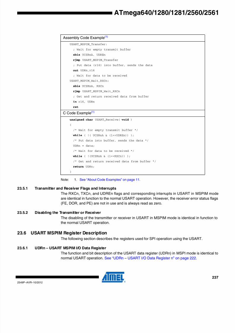
8/20/2019 At Mega 1281 Unlocked
http://slidepdf.com/reader/full/at-mega-1281-unlocked 237/446
237
2549P–AVR–10/2012
ATmega640/1280/1281/2560/2561
Note: 1. See “About Code Examples” on page 11.
23.5.1 Transmitter and Receiver Flags and Interrupts
The RXCn, TXCn, and UDREn flags and corresponding interrupts in USART in MSPIM mode
are identical in function to the normal USART operation. However, the receiver error status flags
(FE, DOR, and PE) are not in use and is always read as zero.
23.5.2 Disabling the Transmitter or Receiver
The disabling of the transmitter or receiver in USART in MSPIM mode is identical in function to
the normal USART operation.
23.6 USART MSPIM Register Description
The following section describes the registers used for SPI operation using the USART.
23.6.1 UDRn – USART MSPIM I/O Data Register
The function and bit description of the USART data register (UDRn) in MSPI mode is identical to
normal USART operation. See “UDRn – USART I/O Data Register n” on page 222.
Assembly Code Example(1)
USART_MSPIM_Transfer:
; Wait for empty transmit buffer
sbis UCSRnA, UDREn
rjmp USART_MSPIM_Transfer
; Put data (r16) into buffer, sends the data
out UDRn,r16
; Wait for data to be received
USART_MSPIM_Wait_RXCn:
sbis UCSRnA, RXCn
rjmp USART_MSPIM_Wait_RXCn
; Get and return received data from buffer
in r16, UDRn
ret
C Code Example(1)
unsigned char USART_Receive( void )
{
/* Wait for empty transmit buffer */
while ( !( UCSRnA & (1<<UDREn)) );
/* Put data into buffer, sends the data */
UDRn = data;
/* Wait for data to be received */
while ( !(UCSRnA & (1<<RXCn)) );
/* Get and return received data from buffer */
return UDRn;
}
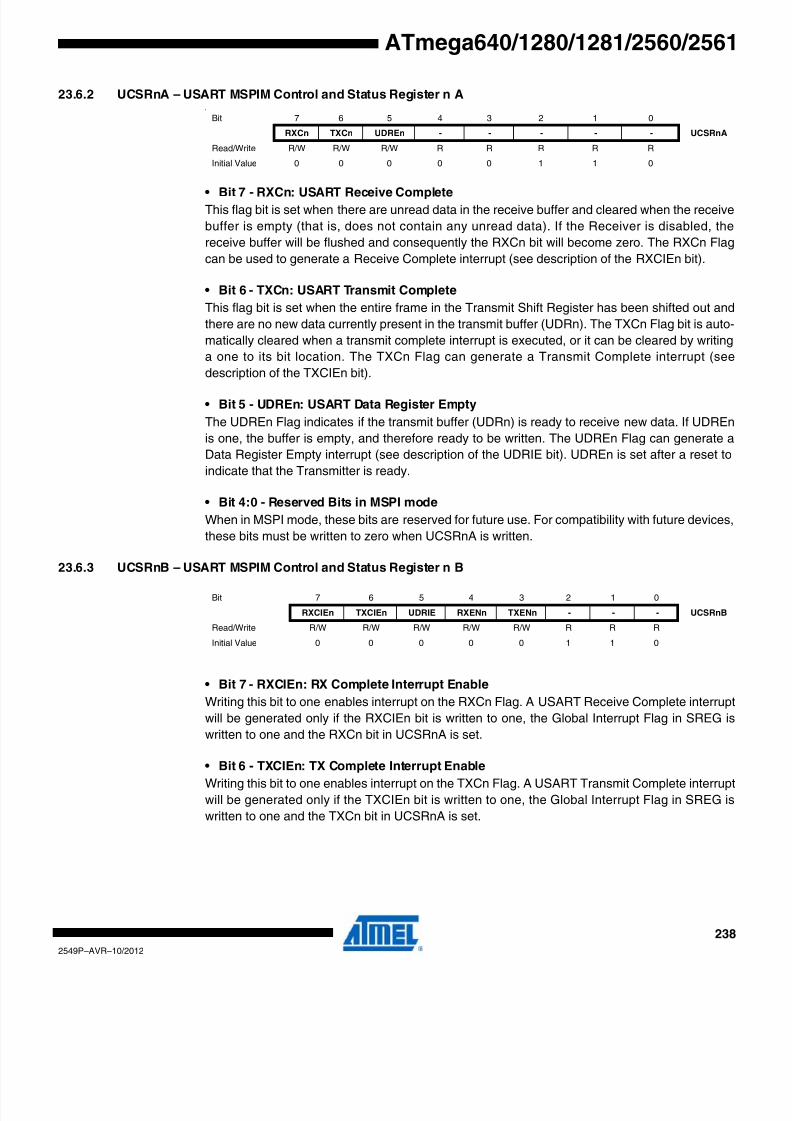
8/20/2019 At Mega 1281 Unlocked
http://slidepdf.com/reader/full/at-mega-1281-unlocked 238/446
238
2549P–AVR–10/2012
ATmega640/1280/1281/2560/2561
23.6.2 UCSRnA – USART MSPIM Control and Status Register n A•
• Bit 7 - RXCn: USART Receive CompleteThis flag bit is set when there are unread data in the receive buffer and cleared when the receive
buffer is empty (that is, does not contain any unread data). If the Receiver is disabled, the
receive buffer will be flushed and consequently the RXCn bit will become zero. The RXCn Flag
can be used to generate a Receive Complete interrupt (see description of the RXCIEn bit).
• Bit 6 - TXCn: USART Transmit Complete
This flag bit is set when the entire frame in the Transmit Shift Register has been shifted out and
there are no new data currently present in the transmit buffer (UDRn). The TXCn Flag bit is auto
matically cleared when a transmit complete interrupt is executed, or it can be cleared by writing
a one to its bit location. The TXCn Flag can generate a Transmit Complete interrupt (see
description of the TXCIEn bit).
• Bit 5 - UDREn: USART Data Register Empty
The UDREn Flag indicates if the transmit buffer (UDRn) is ready to receive new data. If UDREn
is one, the buffer is empty, and therefore ready to be written. The UDREn Flag can generate a
Data Register Empty interrupt (see description of the UDRIE bit). UDREn is set after a reset to
indicate that the Transmitter is ready.
• Bit 4:0 - Reserved Bits in MSPI mode
When in MSPI mode, these bits are reserved for future use. For compatibility with future devices
these bits must be written to zero when UCSRnA is written.
23.6.3 UCSRnB – USART MSPIM Control and Status Register n B
• Bit 7 - RXCIEn: RX Complete Interrupt Enable
Writing this bit to one enables interrupt on the RXCn Flag. A USART Receive Complete interrup
will be generated only if the RXCIEn bit is written to one, the Global Interrupt Flag in SREG is
written to one and the RXCn bit in UCSRnA is set.
• Bit 6 - TXCIEn: TX Complete Interrupt EnableWriting this bit to one enables interrupt on the TXCn Flag. A USART Transmit Complete interrup
will be generated only if the TXCIEn bit is written to one, the Global Interrupt Flag in SREG is
written to one and the TXCn bit in UCSRnA is set.
Bit 7 6 5 4 3 2 1 0
RXCn TXCn UDREn - - - - - UCSRnA
Read/ Write R/ W R/ W R/ W R R R R R
Initial Value 0 0 0 0 0 1 1 0
Bit 7 6 5 4 3 2 1 0
RXCIEn TXCIEn UDRIE RXENn TXENn - - - UCSRnB
Read/ Write R/ W R/ W R/ W R/ W R/ W R R R
Initial Value 0 0 0 0 0 1 1 0
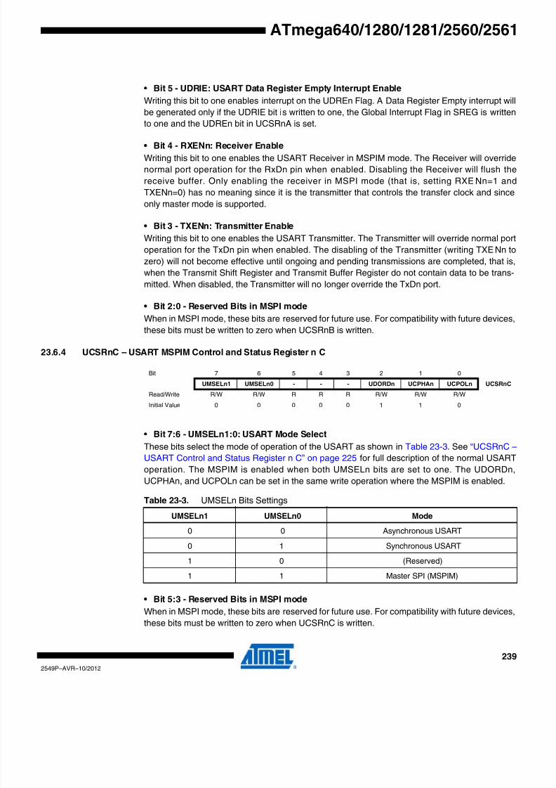
8/20/2019 At Mega 1281 Unlocked
http://slidepdf.com/reader/full/at-mega-1281-unlocked 239/446
239
2549P–AVR–10/2012
ATmega640/1280/1281/2560/2561
• Bit 5 - UDRIE: USART Data Register Empty Interrupt Enable
Writing this bit to one enables interrupt on the UDREn Flag. A Data Register Empty interrupt wil
be generated only if the UDRIE bit is written to one, the Global Interrupt Flag in SREG is written
to one and the UDREn bit in UCSRnA is set.
• Bit 4 - RXENn: Receiver Enable
Writing this bit to one enables the USART Receiver in MSPIM mode. The Receiver will override
normal port operation for the RxDn pin when enabled. Disabling the Receiver will flush the
receive buffer. Only enabling the receiver in MSPI mode (that is, setting RXENn=1 and
TXENn=0) has no meaning since it is the transmitter that controls the transfer clock and since
only master mode is supported.
• Bit 3 - TXENn: Transmitter Enable
Writing this bit to one enables the USART Transmitter. The Transmitter will override normal por
operation for the TxDn pin when enabled. The disabling of the Transmitter (writing TXENn to
zero) will not become effective until ongoing and pending transmissions are completed, that is
when the Transmit Shift Register and Transmit Buffer Register do not contain data to be trans-mitted. When disabled, the Transmitter will no longer override the TxDn port.
• Bit 2:0 - Reserved Bits in MSPI mode
When in MSPI mode, these bits are reserved for future use. For compatibility with future devices
these bits must be written to zero when UCSRnB is written.
23.6.4 UCSRnC – USART MSPIM Control and Status Register n C
• Bit 7:6 - UMSELn1:0: USART Mode Select
These bits select the mode of operation of the USART as shown in Table 23-3. See “UCSRnC –
USART Control and Status Register n C” on page 225 for full description of the normal USART
operation. The MSPIM is enabled when both UMSELn bits are set to one. The UDORDn
UCPHAn, and UCPOLn can be set in the same write operation where the MSPIM is enabled.
• Bit 5:3 - Reserved Bits in MSPI mode
When in MSPI mode, these bits are reserved for future use. For compatibility with future devices
these bits must be written to zero when UCSRnC is written.
Bit 7 6 5 4 3 2 1 0
UMSELn1 UMSELn0 - - - UDORDn UCPHAn UCPOLn UCSRnC
Read/ Write R/ W R/ W R R R R/ W R/ W R/ W
Initial Value 0 0 0 0 0 1 1 0
Table 23-3. UMSELn Bits Settings
UMSELn1 UMSELn0 Mode
0 0 Asynchronous USART
0 1 Synchronous USART
1 0 (Reserved)
1 1 Master SPI (MSPIM)
8/20/2019 At Mega 1281 Unlocked
http://slidepdf.com/reader/full/at-mega-1281-unlocked 240/446
240
2549P–AVR–10/2012
ATmega640/1280/1281/2560/2561
• Bit 2 - UDORDn: Data Order
When set to one the LSB of the data word is transmitted first. When set to zero the MSB of the
data word is transmitted first. Refer to “SPI Data Modes and Timing” on page 233 for details.
• Bit 1 - UCPHAn: Clock Phase
The UCPHAn bit setting determine if data is sampled on the leasing edge (first) or tailing (last)
edge of XCKn. Refer to “SPI Data Modes and Timing” on page 233 for details.
• Bit 0 - UCPOLn: Clock Polarity
The UCPOLn bit sets the polarity of the XCKn clock. The combination of the UCPOLn and
UCPHAn bit settings determine the timing of the data transfer. Refer to “SPI Data Modes and
Timing” on page 233 for details.
23.6.5 UBRRnL and UBRRnH – USART MSPIM Baud Rate Registers
The function and bit description of the baud rate registers in MSPI mode is identical to normal
USART operation. See “UBRRnL and UBRRnH – USART Baud Rate Registers” on page 227.
Table 23-4. Comparison of USART in MSPIM mode and SPI pins.
USART_MSPIM SPI Comment
TxDn MOSI Master Out only
RxDn MISO Master In only
XCKn SCK (Functionally identical)
(N /A) SS Not supported by USART in MSPIM

8/20/2019 At Mega 1281 Unlocked
http://slidepdf.com/reader/full/at-mega-1281-unlocked 241/446
241
2549P–AVR–10/2012
ATmega640/1280/1281/2560/2561
24. 2-wire Serial Interface
24.1 Features• Simple yet Powerful and Flexible Communication Interface, only two Bus Lines needed
• Both Master and Slave Operation Supported
• Device can Operate as Transmitter or Receiver
• 7-bit Address Space Allows up to 128 Different Slave Addresses
• Multi-master Arbitration Support
• Up to 400kHz Data Transfer Speed
• Slew-rate Limited Output Drivers
• Noise Suppression Circuitry Rejects Spikes on Bus Lines
• Fully Programmable Slave Address with General Call Support
• Address Recognition Causes Wake-up When AVR is in Sleep Mode
24.2 2-wire Serial Interface Bus Definition
The 2-wire Serial Interface (TWI) is ideally suited for typical microcontroller applications. The
TWI protocol allows the systems designer to interconnect up to 128 different devices using only
two bi-directional bus lines, one for clock (SCL) and one for data (SDA). The only external hard-ware needed to implement the bus is a single pull-up resistor for each of the TWI bus lines. Al
devices connected to the bus have individual addresses, and mechanisms for resolving bus
contention are inherent in the TWI protocol.
Figure 24-1. TWI Bus Interconnection
24.2.1 TWI Terminology
The following definitions are frequently encountered in this section.
Device 1 Device 2 Device 3 Device n
SDA
SCL
........ R1 R2
VCC
Table 24-1. TWI Terminology
Term Description
MasterThe device that initiates and terminates a transmission. The Master also generates theSCL clock
Slave The device addressed by a Master
Transmitter The device placing data on the bus
Receiver The device reading data from the bus
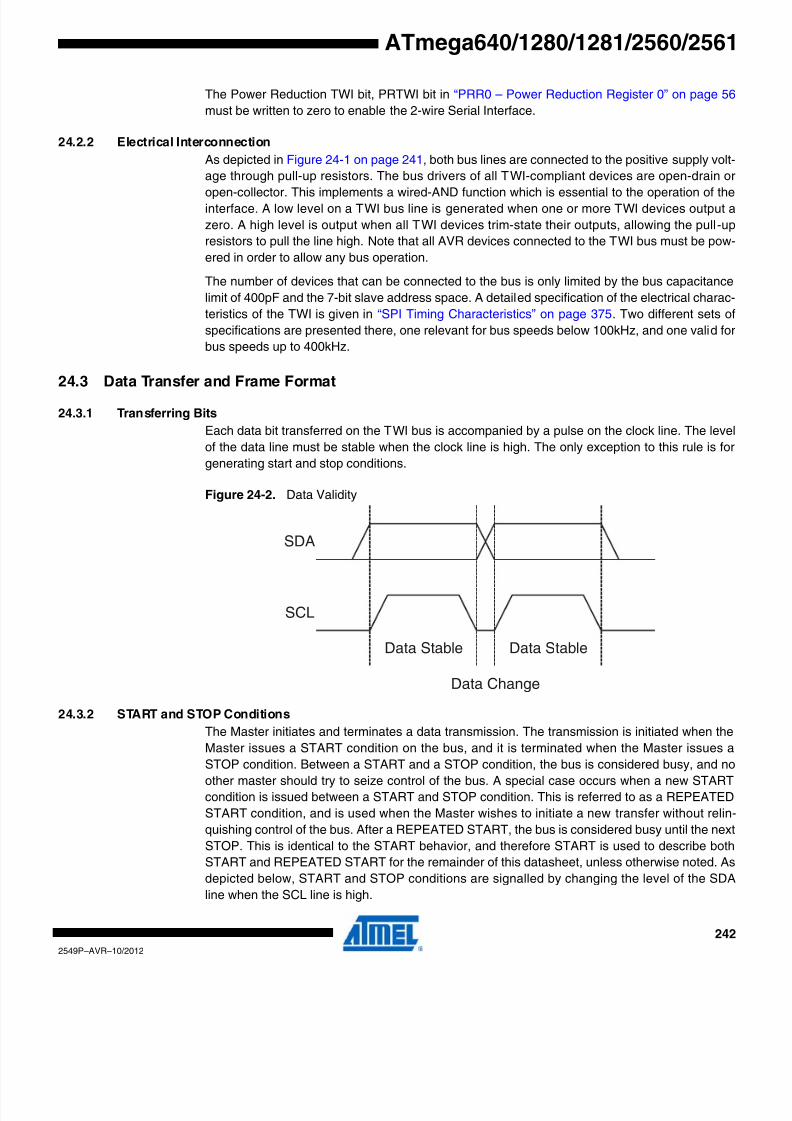
8/20/2019 At Mega 1281 Unlocked
http://slidepdf.com/reader/full/at-mega-1281-unlocked 242/446
242
2549P–AVR–10/2012
ATmega640/1280/1281/2560/2561
The Power Reduction TWI bit, PRTWI bit in “PRR0 – Power Reduction Register 0” on page 56
must be written to zero to enable the 2-wire Serial Interface.
24.2.2 Electrical Interconnection
As depicted in Figure 24-1 on page 241, both bus lines are connected to the positive supply volt
age through pull-up resistors. The bus drivers of all TWI-compliant devices are open-drain o
open-collector. This implements a wired-AND function which is essential to the operation of theinterface. A low level on a TWI bus line is generated when one or more TWI devices output a
zero. A high level is output when all TWI devices trim-state their outputs, allowing the pull-up
resistors to pull the line high. Note that all AVR devices connected to the TWI bus must be pow
ered in order to allow any bus operation.
The number of devices that can be connected to the bus is only limited by the bus capacitance
limit of 400pF and the 7-bit slave address space. A detailed specification of the electrical charac
teristics of the TWI is given in “SPI Timing Characteristics” on page 375. Two different sets o
specifications are presented there, one relevant for bus speeds below 100kHz, and one valid fo
bus speeds up to 400kHz.
24.3 Data Transfer and Frame Format
24.3.1 Transferring Bits
Each data bit transferred on the TWI bus is accompanied by a pulse on the clock line. The leve
of the data line must be stable when the clock line is high. The only exception to this rule is fo
generating start and stop conditions.
Figure 24-2. Data Validity
24.3.2 START and STOP Conditions
The Master initiates and terminates a data transmission. The transmission is initiated when the
Master issues a START condition on the bus, and it is terminated when the Master issues a
STOP condition. Between a START and a STOP condition, the bus is considered busy, and noother master should try to seize control of the bus. A special case occurs when a new START
condition is issued between a START and STOP condition. This is referred to as a REPEATED
START condition, and is used when the Master wishes to initiate a new transfer without relin
quishing control of the bus. After a REPEATED START, the bus is considered busy until the nex
STOP. This is identical to the START behavior, and therefore START is used to describe both
START and REPEATED START for the remainder of this datasheet, unless otherwise noted. As
depicted below, START and STOP conditions are signalled by changing the level of the SDA
line when the SCL line is high.
SDA
SCL
Data Stable Data Stable
Data Change

8/20/2019 At Mega 1281 Unlocked
http://slidepdf.com/reader/full/at-mega-1281-unlocked 243/446
243
2549P–AVR–10/2012
ATmega640/1280/1281/2560/2561
Figure 24-3. START, REPEATED START and STOP conditions
24.3.3 Address Packet Format
All address packets transmitted on the TWI bus are 9 bits long, consisting of 7 address bits, one
READ/ WRITE control bit and an acknowledge bit. If the READ/ WRITE bit is set, a read opera-
tion is to be performed, otherwise a write operation should be performed. When a Slave
recognizes that it is being addressed, it should acknowledge by pulling SDA low in the ninth SCL
(ACK) cycle. If the addressed Slave is busy, or for some other reason can not service the Mas-
ter’s request, the SDA line should be left high in the ACK clock cycle. The Master can then
transmit a STOP condition, or a REPEATED START condition to initiate a new transmission. An
address packet consisting of a slave address and a READ or a WRITE bit is called SLA+R o
SLA+W, respectively.
The MSB of the address byte is transmitted first. Slave addresses can freely be allocated by the
designer, but the address 0000 000 is reserved for a general call.
When a general call is issued, all slaves should respond by pulling the SDA line low in the ACK
cycle. A general call is used when a Master wishes to transmit the same message to severa
slaves in the system. When the general call address followed by a Write bit is transmitted on the
bus, all slaves set up to acknowledge the general call will pull the SDA line low in the ack cycle
The following data packets will then be received by all the slaves that acknowledged the genera
call. Note that transmitting the general call address followed by a Read bit is meaningless, as
this would cause contention if several slaves started transmitting different data.
All addresses of the format 1111 xxx should be reserved for future purposes.
Figure 24-4. Address Packet Format
SDA
SCL
START STOPREPEATED STARTSTOP START
SDA
SCL
START
1 2 7 8 9
Addr MSB Addr LSB R/W ACK

8/20/2019 At Mega 1281 Unlocked
http://slidepdf.com/reader/full/at-mega-1281-unlocked 244/446
244
2549P–AVR–10/2012
ATmega640/1280/1281/2560/2561
24.3.4 Data Packet Format
All data packets transmitted on the TWI bus are nine bits long, consisting of one data byte and
an acknowledge bit. During a data transfer, the Master generates the clock and the START and
STOP conditions, while the Receiver is responsible for acknowledging the reception. An
Acknowledge (ACK) is signalled by the Receiver pulling the SDA line low during the ninth SCL
cycle. If the Receiver leaves the SDA line high, a NACK is signalled. When the Receiver has
received the last byte, or for some reason cannot receive any more bytes, it should inform theTransmitter by sending a NACK after the final byte. The MSB of the data byte is transmitted first.
Figure 24-5. Data Packet Format
24.3.5 Combining Address and Data Packets into a Transmission
A transmission basically consists of a START condition, a SLA+R/ W, one or more data packets
and a STOP condition. An empty message, consisting of a START followed by a STOP condi
tion, is illegal. Note that the Wired-ANDing of the SCL line can be used to implement
handshaking between the Master and the Slave. The Slave can extend the SCL low period by
pulling the SCL line low. This is useful if the clock speed set up by the Master is too fast for the
Slave, or the Slave needs extra time for processing between the data transmissions. The Slave
extending the SCL low period will not affect the SCL high period, which is determined by theMaster. As a consequence, the Slave can reduce the TWI data transfer speed by prolonging the
SCL duty cycle.
Figure 24-6 shows a typical data transmission. Note that several data bytes can be transmitted
between the SLA+R/ W and the STOP condition, depending on the software protocol imple-
mented by the application software.
Figure 24-6. Typical Data Transmission
1 2 7 8 9
Data MSB Data LSB ACK
AggregateSDA
SDA fromTransmitter
SDA fromReceiver
SCL fromMaster
SLA+R/W Data ByteSTOP, REPEATED
START or NextData Byte
1 2 7 8 9
Data Byte
Data MSB Data LSB ACK
SDA
SCL
START
1 2 7 8 9
Addr MSB Addr LSB R/W ACK
SLA+R/W STOP

8/20/2019 At Mega 1281 Unlocked
http://slidepdf.com/reader/full/at-mega-1281-unlocked 245/446
245
2549P–AVR–10/2012
ATmega640/1280/1281/2560/2561
24.4 Multi-master Bus Systems, Arbitration and Synchronization
The TWI protocol allows bus systems with several masters. Special concerns have been taken
in order to ensure that transmissions will proceed as normal, even if two or more masters initiate
a transmission at the same time. Two problems arise in multi-master systems:
• An algorithm must be implemented allowing only one of the masters to complete the
transmission. All other masters should cease transmission when they discover that theyhave lost the selection process. This selection process is called arbitration. When acontending master discovers that it has lost the arbitration process, it should immediatelyswitch to Slave mode to check whether it is being addressed by the winning master. The factthat multiple masters have started transmission at the same time should not be detectable tothe slaves, that is, the data being transferred on the bus must not be corrupted.
• Different masters may use different SCL frequencies. A scheme must be devised tosynchronize the serial clocks from all masters, in order to let the transmission proceed in alockstep fashion. This will facilitate the arbitration process.
The wired-ANDing of the bus lines is used to solve both these problems. The serial clocks from
all masters will be wired-ANDed, yielding a combined clock with a high period equal to the one
from the Master with the shortest high period. The low period of the combined clock is equal to
the low period of the Master with the longest low period.N
ote that all masters listen to the SCLline, effectively starting to count their SCL high and low time-out periods when the combined
SCL line goes high or low, respectively.
Figure 24-7. SCL Synchronization Between Multiple Masters
Arbitration is carried out by all masters continuously monitoring the SDA line after outputtingdata. If the value read from the SDA line does not match the value the Master had output, it has
lost the arbitration. Note that a Master can only lose arbitration when it outputs a high SDA value
while another Master outputs a low value. The losing Master should immediately go to Slave
mode, checking if it is being addressed by the winning Master. The SDA line should be left high
but losing masters are allowed to generate a clock signal until the end of the current data or
address packet. Arbitration will continue until only one Master remains, and this may take many
bits. If several masters are trying to address the same Slave, arbitration will continue into the
data packet.
TAlow
TAhigh
SCL fromMaster A
SCL fromMaster B
SCL BusLine
TBlow
TBhigh
Masters StartCounting Low Period
Masters StartCounting High Period

8/20/2019 At Mega 1281 Unlocked
http://slidepdf.com/reader/full/at-mega-1281-unlocked 246/446
246
2549P–AVR–10/2012
ATmega640/1280/1281/2560/2561
Figure 24-8. Arbitration Between Two Masters
Note that arbitration is not allowed between:
• A REPEATED START condition and a data bit
• A STOP condition and a data bit
• A REPEATED START and a STOP condition
It is the user software’s responsibility to ensure that these illegal arbitration conditions never
occur. This implies that in multi-master systems, all data transfers must use the same composi
tion of SLA+R/ W and data packets. In other words: All transmissions must contain the same
number of data packets, otherwise the result of the arbitration is undefined.
24.5 Overview of the TWI ModuleThe TWI module is comprised of several submodules, as shown in Figure 24-9 on page 247. Al
registers drawn in a thick line are accessible through the AVR data bus.
SDA fromMaster A
SDA fromMaster B
SDA Line
SynchronizedSCL Line
START Master A LosesArbitration, SDAA SDA

8/20/2019 At Mega 1281 Unlocked
http://slidepdf.com/reader/full/at-mega-1281-unlocked 247/446
247
2549P–AVR–10/2012
ATmega640/1280/1281/2560/2561
Figure 24-9. Overview of the TWI Module
24.5.1 SCL and SDA Pins
These pins interface the AVR TWI with the rest of the MCU system. The output drivers contain a
slew-rate limiter in order to conform to the TWI specification. The input stages contain a spike
suppression unit removing spikes shorter than 50ns. Note that the internal pull-ups in the AVR
pads can be enabled by setting the PORT bits corresponding to the SCL and SDA pins, as
explained in the I/O Port section. The internal pull-ups can in some systems eliminate the need
for external ones.
24.5.2 Bit Rate Generator Unit
This unit controls the period of SCL when operating in a Master mode. The SCL period is con-
trolled by settings in the TWI Bit Rate Register (TWBR) and the Prescaler bits in the TWI Status
Register (TWSR). Slave operation does not depend on Bit Rate or Prescaler settings, but the
CPU clock frequency in the Slave must be at least 16 times higher than the SCL frequency. Note
that slaves may prolong the SCL low period, thereby reducing the average TWI bus clock
period.
T W I U n i t
Address Register(TWAR)
Address Match Unit
Address Comparator
Control Unit
Control Register(TWCR)
Status Register(TWSR)
State Machine andStatus control
SCL
Slew-rateControl
SpikeFilter
SDA
Slew-rateControl
SpikeFilter
Bit Rate Generator
Bit Rate Register(TWBR)
Prescaler
Bus Interface Unit
START / STOPControl
Arbitration detection Ack
Spike Suppression
Address/Data ShiftRegister (TWDR)

8/20/2019 At Mega 1281 Unlocked
http://slidepdf.com/reader/full/at-mega-1281-unlocked 248/446
248
2549P–AVR–10/2012
ATmega640/1280/1281/2560/2561
The SCL frequency is generated according to the following equation:
• TWBR = Value of the TWI Bit Rate Register
• TWPS = Value of the prescaler bits in the TWI Status RegisterNote: Pull-up resistor values should be selected according to the SCL frequency and the capacitive bus
line load. See “2-wire Serial Interface Characteristics” on page 373 for value of pull-up resistor.
24.5.3 Bus Interface Unit
This unit contains the Data and Address Shift Register (TWDR), a START/STOP Controller and
Arbitration detection hardware. The TWDR contains the address or data bytes to be transmitted
or the address or data bytes received. In addition to the 8-bit TWDR, the Bus Interface Unit also
contains a register containing the (N)ACK bit to be transmitted or received. This (N)ACK Regis
ter is not directly accessible by the application software. However, when receiving, it can be set
or cleared by manipulating the TWI Control Register (TWCR). When in Transmitter mode, the
value of the received (N)ACK bit can be determined by the value in the TWSR.
The START/STOP Controller is responsible for generation and detection of START, REPEATED
START, and STOP conditions. The START/STOP controller is able to detect START and STOP
conditions even when the AVR MCU is in one of the sleep modes, enabling the MCU to wake up
if addressed by a Master.
If the TWI has initiated a transmission as Master, the Arbitration Detection hardware continu
ously monitors the transmission trying to determine if arbitration is in process. If the TWI has los
an arbitration, the Control Unit is informed. Correct action can then be taken and appropriate
status codes generated.
24.5.4 Address Match Unit
The Address Match unit checks if received address bytes match the seven-bit address in the
TWI Address Register (TWAR). If the TWI General Call Recognition Enable (TWGCE) bit in theTWAR is written to one, all incoming address bits will also be compared against the General Cal
address. Upon an address match, the Control Unit is informed, allowing correct action to be
taken. The TWI may or may not acknowledge its address, depending on settings in the TWCR
The Address Match unit is able to compare addresses even when the AVR MCU is in sleep
mode, enabling the MCU to wake up if addressed by a Master. If another interrupt (for example
INT0) occurs during TWI Power-down address match and wakes up the CPU, the TWI aborts
operation and return to it’s idle state. If this cause any problems, ensure that TWI Address Match
is the only enabled interrupt when entering Power-down.
24.5.5 Control Unit
The Control unit monitors the TWI bus and generates responses corresponding to settings in the
TWI Control Register (TWCR). When an event requiring the attention of the application occurs
on the TWI bus, the TWI Interrupt Flag (TWINT) is asserted. In the next clock cycle, the TWI Sta
tus Register (TWSR) is updated with a status code identifying the event. The TWSR only
contains relevant status information when the TWI Interrupt Flag is asserted. At all other times
the TWSR contains a special status code indicating that no relevant status information is avail
able. As long as the TWINT Flag is set, the SCL line is held low. This allows the application
software to complete its tasks before allowing the TWI transmission to continue.
SCL frequency CPU Clock frequency
16 2(TWBR) 4TWPS
⋅+
-----------------------------------------------------------=
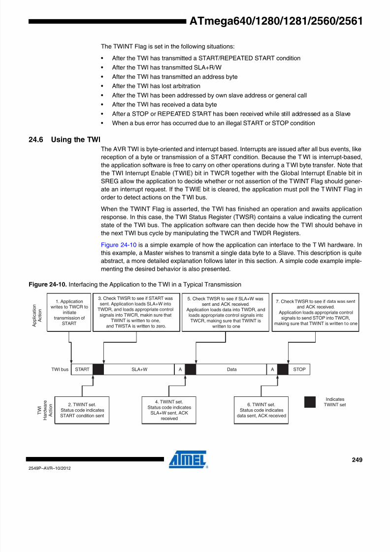
8/20/2019 At Mega 1281 Unlocked
http://slidepdf.com/reader/full/at-mega-1281-unlocked 249/446
249
2549P–AVR–10/2012
ATmega640/1280/1281/2560/2561
The TWINT Flag is set in the following situations:
• After the TWI has transmitted a START/REPEATED START condition
• After the TWI has transmitted SLA+R/ W
• After the TWI has transmitted an address byte
• After the TWI has lost arbitration
• After the TWI has been addressed by own slave address or general call• After the TWI has received a data byte
• After a STOP or REPEATED START has been received while still addressed as a Slave
• When a bus error has occurred due to an illegal START or STOP condition
24.6 Using the TWI
The AVR TWI is byte-oriented and interrupt based. Interrupts are issued after all bus events, like
reception of a byte or transmission of a START condition. Because the TWI is interrupt-based
the application software is free to carry on other operations during a TWI byte transfer. Note tha
the TWI Interrupt Enable (TWIE) bit in TWCR together with the Global Interrupt Enable bit in
SREG allow the application to decide whether or not assertion of the TWINT Flag should gener
ate an interrupt request. If the TWIE bit is cleared, the application must poll the TWINT Flag inorder to detect actions on the TWI bus.
When the TWINT Flag is asserted, the TWI has finished an operation and awaits application
response. In this case, the TWI Status Register (TWSR) contains a value indicating the curren
state of the TWI bus. The application software can then decide how the TWI should behave in
the next TWI bus cycle by manipulating the TWCR and TWDR Registers.
Figure 24-10 is a simple example of how the application can interface to the T WI hardware. In
this example, a Master wishes to transmit a single data byte to a Slave. This description is quite
abstract, a more detailed explanation follows later in this section. A simple code example imple-
menting the desired behavior is also presented.
Figure 24-10. Interfacing the Application to the TWI in a Typical Transmission
START SLA+W A Data A STOP
1. Applicationwrites to TWCR to
initiatetransmission of
START
2. TWINT set.Status code indicatesSTART condition sent
4. TWINT set.Status code indicates
SLA+W sent, ACKreceived
6. TWINT set.Status code indicates
data sent, ACK received
3. Check TWSR to see if START wassent. Application loads SLA+W into
TWDR, and loads appropriate controlsignals into TWCR, makin sure that
TWINT is written to one,and TWSTA is written to zero.
5. Check TWSR to see if SLA+W wassent and ACK received.
Application loads data into TWDR, andloads appropriate control signals intoTWCR, making sure that TWINT is
written to one
7. Check TWSR to see if data was sentand ACK received.
Application loads appropriate controlsignals to send STOP into TWCR,
making sure that TWINT is written to one
TWI bus
IndicatesTWINT set
A p p l i c a t i o n
A c t i o n
T W I
H a r d w a r e
A c t i o n

8/20/2019 At Mega 1281 Unlocked
http://slidepdf.com/reader/full/at-mega-1281-unlocked 250/446
250
2549P–AVR–10/2012
ATmega640/1280/1281/2560/2561
1. The first step in a TWI transmission is to transmit a START condition. This is done bywriting a specific value into TWCR, instructing the TWI hardware to transmit a STARTcondition. Which value to write is described later on. However, it is important that theTWINT bit is set in the value written. Writing a one to TWINT clears the flag. The TWI willnot start any operation as long as the TWINT bit in TWCR is set. Immediately after theapplication has cleared TWINT, the TWI will initiate transmission of the START condition.
2. When the START condition has been transmitted, the TWINT Flag in TWCR is set, andTWSR is updated with a status code indicating that the START condition has success-fully been sent.
3. The application software should now examine the value of TWSR, to make sure that theSTART condition was successfully transmitted. If TWSR indicates otherwise, the applica-tion software might take some special action, like calling an error routine. Assuming thatthe status code is as expected, the application must load SLA+W into TWDR. Rememberthat TWDR is used both for address and data. After TWDR has been loaded with thedesired SLA+W, a specific value must be written to TWCR, instructing the TWI hardwareto transmit the SLA+W present in TWDR. Which value to write is described later on.However, it is important that the TWINT bit is set in the value written. Writing a one toTWINT clears the flag. The TWI will not start any operation as long as the TWINT bit inTWCR is set. Immediately after the application has cleared TWINT, the TWI will initiate
transmission of the address packet.
4. When the address packet has been transmitted, the TWINT Flag in TWCR is set, andTWSR is updated with a status code indicating that the address packet has successfullybeen sent. The status code will also reflect whether a Slave acknowledged the packet ornot.
5. The application software should now examine the value of TWSR, to make sure that theaddress packet was successfully transmitted, and that the value of the ACK bit was asexpected. If TWSR indicates otherwise, the application software might take some specialaction, like calling an error routine. Assuming that the status code is as expected, theapplication must load a data packet into TWDR. Subsequently, a specific value must bewritten to TWCR, instructing the TWI hardware to transmit the data packet present inTWDR. Which value to write is described later on. However, it is important that the
TWINT bit is set in the value written. Writing a one to TWINT clears the flag. The TWI willnot start any operation as long as the TWINT bit in TWCR is set. Immediately after theapplication has cleared TWINT, the TWI will initiate transmission of the data packet.
6. When the data packet has been transmitted, the TWINT Flag in TWCR is set, and TWSRis updated with a status code indicating that the data packet has successfully been sent.The status code will also reflect whether a Slave acknowledged the packet or not.
7. The application software should now examine the value of TWSR, to make sure that thedata packet was successfully transmitted, and that the value of the ACK bit was asexpected. If TWSR indicates otherwise, the application software might take some specialaction, like calling an error routine. Assuming that the status code is as expected, theapplication must write a specific value to TWCR, instructing the TWI hardware to transmita STOP condition. Which value to write is described later on. However, it is important that
the TWINT bit is set in the value written. Writing a one to TWINT clears the flag. The TWIwill not start any operation as long as the TWINT bit in TWCR is set. Immediately afterthe application has cleared TWINT, the TWI will initiate transmission of the STOP condi-tion. Note that TWINT is NOT set after a STOP condition has been sent.

8/20/2019 At Mega 1281 Unlocked
http://slidepdf.com/reader/full/at-mega-1281-unlocked 251/446
251
2549P–AVR–10/2012
ATmega640/1280/1281/2560/2561
Even though this example is simple, it shows the principles involved in all TWI transmissions
These can be summarized as follows:
• When the TWI has finished an operation and expects application response, the TWINT Flagis set. The SCL line is pulled low until TWINT is cleared.
• When the TWINT Flag is set, the user must update all TWI Registers with the value relevantfor the next TWI bus cycle. As an example, TWDR must be loaded with the value to betransmitted in the next bus cycle.
• After all TWI Register updates and other pending application software tasks have beencompleted, TWCR is written. When writing TWCR, the TWINT bit should be set. Writing aone to TWINT clears the flag. The TWI will then commence executing whatever operationwas specified by the TWCR setting.
In the following an assembly and C implementation of the example is given. Note that the code
below assumes that several definitions have been made, for example by using include-files.
Assembly Code Example C Example Comments
1 ldi r16, (1<<TWINT)|(1<<TWSTA)|(1<<TWEN)
out TWCR, r16
TWCR = (1<<TWINT)|(1<<TWSTA)|(1<<TWEN) Send START condition
2 wait1:
in r16,TWCR
sbrs r16,TWINT
rjmp wait1
while (!(TWCR & (1<<TWINT)))
; Wait for TWINT Flag set. Thisindicates that the START condition
has been transmitted
3 in r16,TWSR
andi r16, 0xF8
cpi r16, START
brne ERROR
if ((TWSR & 0xF8) != START)
ERROR();Check value of TWI Status
Register. Mask prescaler bits. Ifstatus different from START go to
ERROR
ldi r16, SLA_Wout TWDR, r16
ldi r16, (1<<TWINT) | (1<<TWEN)
out TWCR, r16
TWDR = SLA_W;TWCR = (1<<TWINT) | (1<<TWEN); Load SLA_W into TWDR Register.
Clear TWINT bit in TWCR to starttransmission of address
4 wait2:
in r16,TWCR
sbrs r16,TWINT
rjmp wait2
while (!(TWCR & (1<<TWINT)))
;Wait for TWINT Flag set. This
indicates that the SLA+W has beentransmitted, and ACK/ NACK has
been received.
5 in r16,TWSR
andi r16, 0xF8
cpi r16, MT_SLA_ACK
brne ERROR
if ((TWSR & 0xF8) !=MT_SLA_ACK)
ERROR();
Check value of TWI StatusRegister. Mask prescaler bits. If
status different from MT_SLA_ACKgo to ERROR
ldi r16, DATA
out TWDR, r16
ldi r16, (1<<TWINT) | (1<<TWEN)
out TWCR, r16
TWDR = DATA;
TWCR = (1<<TWINT) | (1<<TWEN); Load DATA into TWDR Register.Clear TWINT bit in TWCR to start
transmission of data
8/20/2019 At Mega 1281 Unlocked
http://slidepdf.com/reader/full/at-mega-1281-unlocked 252/446
252
2549P–AVR–10/2012
ATmega640/1280/1281/2560/2561
24.7 Transmission Modes
The TWI can operate in one of four major modes. These are named Master Transmitter (MT)
Master Receiver (MR), Slave Transmitter (ST) and Slave Receiver (SR). Several of these
modes can be used in the same application. As an example, the TWI can use MT mode to write
data into a TWI EEPROM, MR mode to read the data back from the EEPROM. If other masters
are present in the system, some of these might transmit data to the T WI, and then SR mode
would be used. It is the application software that decides which modes are legal.
The following sections describe each of these modes. Possible status codes are described
along with figures detailing data transmission in each of the modes. These figures contain the
following abbreviations:
S: START condition
Rs: REPEATED START condition
R: Read bit (high level at SDA)
W: Write bit (low level at SDA)
A: Acknowledge bit (low level at SDA)
A: Not acknowledge bit (high level at SDA)
Data: 8-bit data byte
P: STOP condition
SLA: Slave Address
In Figure 24-12 on page 255 to Figure 24-18 on page 264, circles are used to indicate that the
TWINT Flag is set. The numbers in the circles show the status code held in TWSR, with the
prescaler bits masked to zero. At these points, actions must be taken by the application to con-
tinue or complete the TWI transfer. The TWI transfer is suspended until the TWINT Flag iscleared by software.
When the TWINT Flag is set, the status code in TWSR is used to determine the appropriate soft
ware action. For each status code, the required software action and details of the following seria
transfer are given in Table 24-2 on page 254 to Table 24-5 on page 263. Note that the prescale
bits are masked to zero in these tables.
6 wait3:
in r16,TWCR
sbrs r16,TWINT
rjmp wait3
while (!(TWCR & (1<<TWINT)))
;Wait for TWINT Flag set. This
indicates that the DATA has beentransmitted, and ACK/ NACK has
been received.
7 in r16,TWSRandi r16, 0xF8
cpi r16, MT_DATA_ACK
brne ERROR
if ((TWSR & 0xF8) !=MT_DATA_ACK)
ERROR();
Check value of TWI StatusRegister. Mask prescaler bits. If
status different fromMT_DATA_ACK go to ERROR
ldi r16, (1<<TWINT)|(1<<TWEN)|
(1<<TWSTO)
out TWCR, r16
TWCR = (1<<TWINT)|(1<<TWEN)|
(1<<TWSTO); Transmit STOP condition
Assembly Code Example C Example Comments

8/20/2019 At Mega 1281 Unlocked
http://slidepdf.com/reader/full/at-mega-1281-unlocked 253/446
253
2549P–AVR–10/2012
ATmega640/1280/1281/2560/2561
24.7.1 Master Transmitter Mode
In the Master Transmitter mode, a number of data bytes are transmitted to a Slave Receiver
(see Figure 24-11). In order to enter a Master mode, a START condition must be transmitted
The format of the following address packet determines whether Master Transmitter or Maste
Receiver mode is to be entered. If SLA+W is transmitted, MT mode is entered, if SLA+R is trans
mitted, MR mode is entered. All the status codes mentioned in this section assume that the
prescaler bits are zero or are masked to zero.
Figure 24-11. Data Transfer in Master Transmitter Mode
A START condition is sent by writing the following value to TWCR:
TWEN must be set to enable the 2-wire Serial Interface, TWSTA must be written to one to trans
mit a START condition and TWINT must be written to one to clear the TWINT Flag. The TWI wil
then test the 2-wire Serial Bus and generate a START condition as soon as the bus becomes
free. After a START condition has been transmitted, the TWINT Flag is set by hardware, and the
status code in TWSR will be 0x08 (see Table 24-2 on page 254). In order to enter MT mode
SLA+W must be transmitted. This is done by writing SLA+W to TWDR. Thereafter the TWINT bi
should be cleared (by writing it to one) to continue the transfer. This is accomplished by writing
the following value to TWCR:
When SLA+W have been transmitted and an acknowledgement bit has been received, TWINT is
set again and a number of status codes in TWSR are possible. Possible status codes in Maste
mode are 0x18, 0x20, or 0x38. The appropriate action to be taken for each of these status codes
is detailed in Table 24-2 on page 254.
When SLA+W has been successfully transmitted, a data packet should be transmitted. This is
done by writing the data byte to TWDR. TWDR must only be written when TWINT is high. If notthe access will be discarded, and the Write Collision bit (TWWC) will be set in the TWCR Regis
ter. After updating TWDR, the TWINT bit should be cleared (by writing it to one) to continue the
transfer. This is accomplished by writing the following value to TWCR:
TWCR TWINT TWEA TWSTA TWSTO TWWC TWEN – TWIE
value 1 X 1 0 X 1 0 X
TWCR TWINT TWEA TWSTA TWSTO TWWC TWEN – TWIE
value 1 X 0 0 X 1 0 X
TWCR TWINT TWEA TWSTA TWSTO TWWC TWEN – TWIE
value 1 X 0 0 X 1 0 X
Device 1MASTER
TRANSMITTER
Device 2SLAVE
RECEIVER
Device 3 Device n
SDA
SCL
........ R1 R2
VCC

8/20/2019 At Mega 1281 Unlocked
http://slidepdf.com/reader/full/at-mega-1281-unlocked 254/446
254
2549P–AVR–10/2012
ATmega640/1280/1281/2560/2561
This scheme is repeated until the last byte has been sent and the transfer is ended by generat-
ing a STOP condition or a repeated START condition. A STOP condition is generated by writing
the following value to TWCR:
A REPEATED START condition is generated by writing the following value to TWCR:
After a repeated START condition (state 0x10) the 2-wire Serial Interface can access the same
Slave again, or a new Slave without transmitting a STOP condition. Repeated START enables
the Master to switch between Slaves, Master Transmitter mode and Master Receiver mode with-
out losing control of the bus.
TWCR TWINT TWEA TWSTA TWSTO TWWC TWEN – TWIE
value 1 X 0 1 X 1 0 X
TWCR TWINT TWEA TWSTA TWSTO TWWC TWEN – TWIE
value 1 X 1 0 X 1 0 X
Table 24-2. Status codes for Master Transmitter Mode
Status Code(TWSR)Prescaler Bitsare 0
Status of the 2-wire Serial Busand 2-wire Serial Interface Hard-ware
Application Software Response
Next Action Taken by TWI Hardware
To/from TWDR To TWCR
STA STO TWINT TWEA
0x08 A START condition has beentransmitted
Load SLA+W 0 0 1 X SLA+W will be transmitted; ACK or NOT ACK will be received
0x10 A repeated START conditionhas been transmitted
Load SLA+W or
Load SLA+R
0
0
0
0
1
1
X
X
SLA+W will be transmitted; ACK or NOT ACK will be receivedSLA+R will be transmitted;Logic will switch to Master Receiver mode
0x18 SLA+W has been transmitted; ACK has been received
Load data byte or
No TWDR action or No TWDR action or
No TWDR action
0
10
1
0
01
1
1
11
1
X
XX
X
Data byte will be transmitted and ACK or NOT ACK willbe receivedRepeated START will be transmittedSTOP condition will be transmitted andTWSTO Flag will be resetSTOP condition followed by a START condition will betransmitted and TWSTO Flag will be reset
0x20 SLA+W has been transmitted;NOT ACK has been received
Load data byte or
No TWDR action or No TWDR action or
No TWDR action
0
10
1
0
01
1
1
11
1
X
XX
X
Data byte will be transmitted and ACK or NOT ACK willbe receivedRepeated START will be transmittedSTOP condition will be transmitted and
TWSTO Flag will be resetSTOP condition followed by a START condition will betransmitted and TWSTO Flag will be reset
0x28 Data byte has been transmitted; ACK has been received
Load data byte or
No TWDR action or No TWDR action or
No TWDR action
0
10
1
0
01
1
1
11
1
X
XX
X
Data byte will be transmitted and ACK or NOT ACK willbe receivedRepeated START will be transmittedSTOP condition will be transmitted andTWSTO Flag will be resetSTOP condition followed by a START condition will betransmitted and TWSTO Flag will be reset
0x30 Data byte has been transmitted;NOT ACK has been received
Load data byte or
No TWDR action or No TWDR action or
No TWDR action
0
10
1
0
01
1
1
11
1
X
XX
X
Data byte will be transmitted and ACK or NOT ACK willbe receivedRepeated START will be transmittedSTOP condition will be transmitted andTWSTO Flag will be resetSTOP condition followed by a START condition will betransmitted and TWSTO Flag will be reset
0x38 Arbitration lost in SLA+W or data
bytes
No TWDR action or
No TWDR action
0
1
0
0
1
1
X
X
2-wire Serial Bus will be released and not addressed
Slave mode entered A START condition will be transmitted when the bus be-comes free
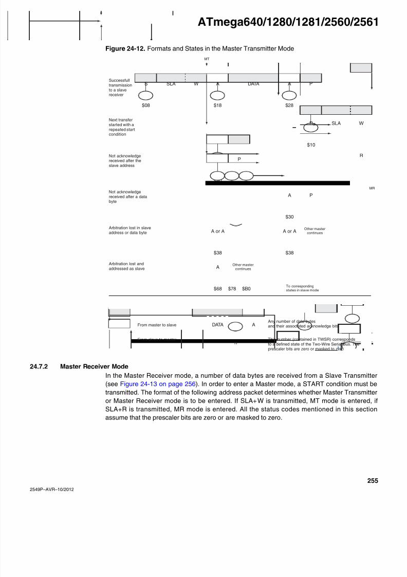
8/20/2019 At Mega 1281 Unlocked
http://slidepdf.com/reader/full/at-mega-1281-unlocked 255/446
255
2549P–AVR–10/2012
ATmega640/1280/1281/2560/2561
Figure 24-12. Formats and States in the Master Transmitter Mode
24.7.2 Master Receiver Mode
In the Master Receiver mode, a number of data bytes are received from a Slave Transmitte
(see Figure 24-13 on page 256). In order to enter a Master mode, a START condition must be
transmitted. The format of the following address packet determines whether Master Transmitteor Master Receiver mode is to be entered. If SLA+W is transmitted, MT mode is entered, i
SLA+R is transmitted, MR mode is entered. All the status codes mentioned in this section
assume that the prescaler bits are zero or are masked to zero.
S SLA W A DATA A P
$08 $18 $28
R SLA W
$10
A P
$20
P
$30
A or A
$38
A
Other mastercontinues A or A
$38
Other mastercontinues
R
A
$68
Other mastercontinues
$78 $B0To correspondingstates in slave mode
MT
MR
Successfulltransmissionto a slavereceiver
Next transferstarted with arepeated startcondition
Not acknowledgereceived after theslave address
Not acknowledge
received after a databyte
Arbitration lost in slaveaddress or data byte
Arbitration lost andaddressed as slave
DATA A
n
From master to slave
From slave to master
Any number of data bytesand their associated acknowledge bits
This number (contained in TWSR) correspondsto a defined state of the Two-Wire Serial Bus. Theprescaler bits are zero or masked to zero
S

8/20/2019 At Mega 1281 Unlocked
http://slidepdf.com/reader/full/at-mega-1281-unlocked 256/446
256
2549P–AVR–10/2012
ATmega640/1280/1281/2560/2561
Figure 24-13. Data Transfer in Master Receiver Mode
A START condition is sent by writing the following value to TWCR:
TWEN must be written to one to enable the 2-wire Serial Interface, TWSTA must be written to
one to transmit a START condition and TWINT must be set to clear the TWINT Flag. The TW
will then test the 2-wire Serial Bus and generate a START condition as soon as the bus
becomes free. After a START condition has been transmitted, the TWINT Flag is set by hard
ware, and the status code in TWSR will be 0x08 (see Table 24-2 on page 254). In order to ente
MR mode, SLA+R must be transmitted. This is done by writing SLA+R to TWDR. Thereafter the
TWINT bit should be cleared (by writing it to one) to continue the transfer. This is accomplished
by writing the following value to TWCR:
When SLA+R have been transmitted and an acknowledgement bit has been received, TWINT is
set again and a number of status codes in TWSR are possible. Possible status codes in Maste
mode are 0x38, 0x40, or 0x48. The appropriate action to be taken for each of these status codesis detailed in Table 24-3 on page 257. Received data can be read from the TWDR Registe
when the TWINT Flag is set high by hardware. This scheme is repeated until the last byte has
been received. After the last byte has been received, the MR should inform the ST by sending a
NACK after the last received data byte. The transfer is ended by generating a STOP condition o
a repeated START condition. A STOP condition is generated by writing the following value to
TWCR:
A REPEATED START condition is generated by writing the following value to TWCR:
After a repeated START condition (state 0x10) the 2-wire Serial Interface can access the same
Slave again, or a new Slave without transmitting a STOP condition. Repeated START enables
the Master to switch between Slaves, Master Transmitter mode and Master Receiver mode with-
out losing control over the bus.
TWCR TWINT TWEA TWSTA TWSTO TWWC TWEN – TWIE
value 1 X 1 0 X 1 0 X
TWCR TWINT TWEA TWSTA TWSTO TWWC TWEN – TWIE
value 1 X 0 0 X 1 0 X
TWCR TWINT TWEA TWSTA TWSTO TWWC TWEN – TWIE
value 1 X 0 1 X 1 0 X
TWCR TWINT TWEA TWSTA TWSTO TWWC TWEN – TWIE
value 1 X 1 0 X 1 0 X
Device 1MASTER
RECEIVER
Device 2SLAVE
TRANSMITTER
Device 3 Device n
SDA
SCL
........ R1 R2
VCC
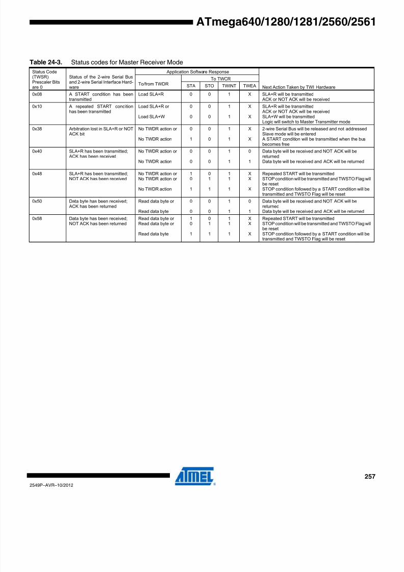
8/20/2019 At Mega 1281 Unlocked
http://slidepdf.com/reader/full/at-mega-1281-unlocked 257/446
257
2549P–AVR–10/2012
ATmega640/1280/1281/2560/2561
Table 24-3. Status codes for Master Receiver Mode
Status Code(TWSR)Prescaler Bitsare 0
Status of the 2-wire Serial Busand 2-wire Serial Interface Hard-ware
Application Software Response
Next Action Taken by TWI HardwareTo/from TWDR
To TWCR
STA STO TWINT TWEA
0x08 A START condition has beentransmitted
Load SLA+R 0 0 1 X SLA+R will be transmitted ACK or NOT ACK will be received
0x10 A repeated START conditionhas been transmitted
Load SLA+R or
Load SLA+W
0
0
0
0
1
1
X
X
SLA+R will be transmitted ACK or NOT ACK will be receivedSLA+W will be transmittedLogic will switch to Master Transmitter mode
0x38 Arbitration lost in SLA+R or NOT ACK bit
No TWDR action or
No TWDR action
0
1
0
0
1
1
X
X
2-wire Serial Bus will be released and not addressedSlave mode will be entered A START condition will be transmitted when the busbecomes free
0x40 SLA+R has been transmitted; ACK has been received
No TWDR action or
No TWDR action
0
0
0
0
1
1
0
1
Data byte will be received and NOT ACK will bereturnedData byte will be received and ACK will be returned
0x48 SLA+R has been transmitted;NOT ACK has been received
No TWDR action or No TWDR action or
No TWDR action
10
1
01
1
11
1
XX
X
Repeated START will be transmittedSTOP condition will be transmitted and TWSTO Flag willbe resetSTOP condition followed by a START condition will be
transmitted and TWSTO Flag will be reset0x50 Data byte has been received;
ACK has been returnedRead data byte or
Read data byte
0
0
0
0
1
1
0
1
Data byte will be received and NOT ACK will bereturnedData byte will be received and ACK will be returned
0x58 Data byte has been received;NOT ACK has been returned
Read data byte or Read data byte or
Read data byte
10
1
01
1
11
1
XX
X
Repeated START will be transmittedSTOP condition will be transmitted and TWSTO Flag willbe resetSTOP condition followed by a START condition will betransmitted and TWSTO Flag will be reset

8/20/2019 At Mega 1281 Unlocked
http://slidepdf.com/reader/full/at-mega-1281-unlocked 258/446
258
2549P–AVR–10/2012
ATmega640/1280/1281/2560/2561
Figure 24-14. Formats and States in the Master Receiver Mode
24.7.3 Slave Receiver Mode
In the Slave Receiver mode, a number of data bytes are received from a Master Transmitte(see Figure 24-15). All the status codes mentioned in this section assume that the prescaler bits
are zero or are masked to zero.
Figure 24-15. Data transfer in Slave Receiver mode
To initiate the Slave Receiver mode, TWAR and TWCR must be initialized as follows:
S SLA R A DATA A
$08 $40 $50
SLA R
$10
A P
$48
A or A
$38
Other mastercontinues
$38
Other mastercontinues
W
A
$68
Other mastercontinues
$78 $B0To correspondingstates in slave mode
MR
MT
Successfullreceptionfrom a slavereceiver
Next transferstarted with arepeated startcondition
Not acknowledgereceived after theslave address
Arbitration lost in slaveaddress or data byte
Arbitration lost andaddressed as slave
DATA A
n
From master to slave
From slave to master
Any number of data bytesand their associated acknowledge bits
This number (contained in TWSR) correspondsto a defined state of the Two-Wire Serial Bus. Theprescaler bits are zero or masked to zero
PDATA A
$58
A
RS
TWAR TWA6 TWA5 TWA4 TWA3 TWA2 TWA1 TWA0 TWGCE
value Device’s Own Slave Address
Device 3 Device n
SDA
SCL
........ R1 R2
VCC
Device 2MASTER
TRANSMITTER
Device 1SLAVE
RECEIVER

8/20/2019 At Mega 1281 Unlocked
http://slidepdf.com/reader/full/at-mega-1281-unlocked 259/446
259
2549P–AVR–10/2012
ATmega640/1280/1281/2560/2561
The upper seven bits are the address to which the 2-wire Serial Interface will respond when
addressed by a Master. If the LSB is set, the TWI will respond to the general call address (0x00)
otherwise it will ignore the general call address.
TWEN must be written to one to enable the TWI. The TWEA bit must be written to one to enablethe acknowledgement of the device’s own slave address or the general call address. TWSTA
and TWSTO must be written to zero.
When TWAR and TWCR have been initialized, the TWI waits until it is addressed by its own
slave address (or the general call address if enabled) followed by the data direction bit. If the
direction bit is “0” (write), the TWI will operate in SR mode, otherwise ST mode is entered. Afte
its own slave address and the write bit have been received, the TWINT Flag is set and a valid
status code can be read from TWSR. The status code is used to determine the appropriate soft
ware action. The appropriate action to be taken for each status code is detailed in Table 24-4 on
page 260. The Slave Receiver mode may also be entered if arbitration is lost while the TWI is in
the Master mode (see states 0x68 and 0x78).
If the TWEA bit is reset during a transfer, the TWI will return a “Not Acknowledge” (“1”) to SDAafter the next received data byte. This can be used to indicate that the Slave is not able to
receive any more bytes. While TWEA is zero, the TWI does not acknowledge its own slave
address. However, the 2-wire Serial Bus is still monitored and address recognition may resume
at any time by setting TWEA. This implies that the TWEA bit may be used to temporarily isolate
the TWI from the 2-wire Serial Bus.
In all sleep modes other than Idle mode, the clock system to the T WI is turned off. If the TWEA
bit is set, the interface can still acknowledge its own slave address or the general call address by
using the 2-wire Serial Bus clock as a clock source. The part will then wake up from sleep and
the TWI will hold the SCL clock low during the wake up and until the TWINT Flag is cleared (by
writing it to one). Further data reception will be carried out as normal, with the AVR clocks run
ning as normal. Observe that if the AVR is set up with a long start-up time, the SCL line may beheld low for a long time, blocking other data transmissions.
Note that the 2-wire Serial Interface Data Register – TWDR does not reflect the last byte presen
on the bus when waking up from these Sleep modes.
TWCR TWINT TWEA TWSTA TWSTO TWWC TWEN – TWIE
value 0 1 0 0 0 1 0 X

8/20/2019 At Mega 1281 Unlocked
http://slidepdf.com/reader/full/at-mega-1281-unlocked 260/446
260
2549P–AVR–10/2012
ATmega640/1280/1281/2560/2561
Table 24-4. Status Codes for Slave Receiver Mode
Status Code(TWSR)Prescaler Bitsare 0
Status of the 2-wire Serial Bus and2-wire Serial Interface Hardware
Application Software Response
Next Action Taken by TWI HardwareTo/from TWDR
To TWCR
STA STO TWINT TWEA
0x60 Own SLA+W has been received; ACK has been returned
No TWDR action or
No TWDR action
X
X
0
0
1
1
0
1
Data byte will be received and NOT ACK will bereturnedData byte will be received and ACK will be returned
0x68 Arbitration lost in SLA+R/W asMaster; own SLA+W has beenreceived; ACK has been returned
No TWDR action or
No TWDR action
X
X
0
0
1
1
0
1
Data byte will be received and NOT ACK will bereturnedData byte will be received and ACK will be returned
0x70 General call address has beenreceived; ACK has been returned
No TWDR action or
No TWDR action
X
X
0
0
1
1
0
1
Data byte will be received and NOT ACK will bereturnedData byte will be received and ACK will be returned
0x78 Arbitration lost in SLA+R/W asMaster; General call address hasbeen received; ACK has beenreturned
No TWDR action or
No TWDR action
X
X
0
0
1
1
0
1
Data byte will be received and NOT ACK will bereturnedData byte will be received and ACK will be returned
0x80 Previously addressed with ownSLA+W; data has been received; ACK has been returned
Read data byte or
Read data byte
X
X
0
0
1
1
0
1
Data byte will be received and NOT ACK will bereturnedData byte will be received and ACK will be returned
0x88 Previously addressed with ownSLA+W; data has been received;NOT ACK has been returned
Read data byte or
Read data byte or
Read data byte or
Read data byte
0
0
1
1
0
0
0
0
1
1
1
1
0
1
0
1
Switched to the not addressed Slave mode;no recognition of own SLA or GCASwitched to the not addressed Slave mode;
own SLA will be recognized;GCA will be recognized if TWGCE = “1”Switched to the not addressed Slave mode;no recognition of own SLA or GCA;a START condition will be transmitted when the busbecomes freeSwitched to the not addressed Slave mode;own SLA will be recognized;GCA will be recognized if TWGCE = “1”;a START condition will be transmitted when the busbecomes free
0x90 Previously addressed withgeneral call; data has been re-ceived; ACK has been returned
Read data byte or
Read data byte
X
X
0
0
1
1
0
1
Data byte will be received and NOT ACK will bereturnedData byte will be received and ACK will be returned
0x98 Previously addressed withgeneral call; data has beenreceived; NOT ACK has beenreturned
Read data byte or
Read data byte or
Read data byte or
Read data byte
0
0
1
1
0
0
0
0
1
1
1
1
0
1
0
1
Switched to the not addressed Slave mode;no recognition of own SLA or GCASwitched to the not addressed Slave mode;own SLA will be recognized;
GCA will be recognized if TWGCE = “1”Switched to the not addressed Slave mode;no recognition of own SLA or GCA;a START condition will be transmitted when the busbecomes freeSwitched to the not addressed Slave mode;own SLA will be recognized;GCA will be recognized if TWGCE = “1”;a START condition will be transmitted when the busbecomes free
0xA0 A STOP condition or repeatedSTART condition has beenreceived while still addressed asSlave
No action 0
0
1
1
0
0
0
0
1
1
1
1
0
1
0
1
Switched to the not addressed Slave mode;no recognition of own SLA or GCASwitched to the not addressed Slave mode;own SLA will be recognized;GCA will be recognized if TWGCE = “1”Switched to the not addressed Slave mode;no recognition of own SLA or GCA;a START condition will be transmitted when the busbecomes free
Switched to the not addressed Slave mode;own SLA will be recognized;GCA will be recognized if TWGCE = “1”;a START condition will be transmitted when the busbecomes free

8/20/2019 At Mega 1281 Unlocked
http://slidepdf.com/reader/full/at-mega-1281-unlocked 261/446
261
2549P–AVR–10/2012
ATmega640/1280/1281/2560/2561
Figure 24-16. Formats and States in the Slave Receiver Mode
24.7.4 Slave Transmitter Mode
In the Slave Transmitter mode, a number of data bytes are transmitted to a Master Receiver
(see Figure 24-17). All the status codes mentioned in this section assume that the prescaler bits
are zero or are masked to zero.
Figure 24-17. Data Transfer in Slave Transmitter Mode
S SLA W A DATA A
$60 $80
$88
A
$68
Reception of the ownslave address and one ormore data bytes. All areacknowledged
Last data byte received
is not acknowledged
Arbitration lost as masterand addressed as slave
Reception of the general calladdress and one or more databytes
Last data byte received isnot acknowledged
n
From master to slave
From slave to master
Any number of data bytesand their associated acknowledge bits
This number (contained in TWSR) correspondsto a defined state of the Two-Wire Serial Bus. Theprescaler bits are zero or masked to zero
P or SDATA A
$80 $A0
P or SA
A DATA A
$70 $90
$98
A
$78
P or SDATA A
$90 $A0
P or SA
General Call
Arbitration lost as master andaddressed as slave by general call
DATA A
Device 3 Device n
SDA
SCL
........ R1 R2
VCC
Device 2MASTER
RECEIVER
Device 1SLAVE
TRANSMITTER
8/20/2019 At Mega 1281 Unlocked
http://slidepdf.com/reader/full/at-mega-1281-unlocked 262/446
262
2549P–AVR–10/2012
ATmega640/1280/1281/2560/2561
To initiate the Slave Transmitter mode, TWAR and TWCR must be initialized as follows:
The upper seven bits are the address to which the 2-wire Serial Interface will respond when
addressed by a Master. If the LSB is set, the TWI will respond to the general call address (0x00)
otherwise it will ignore the general call address.
TWEN must be written to one to enable the TWI. The TWEA bit must be written to one to enable
the acknowledgement of the device’s own slave address or the general call address. TWSTA
and TWSTO must be written to zero.
When TWAR and TWCR have been initialized, the TWI waits until it is addressed by its own
slave address (or the general call address if enabled) followed by the data direction bit. If the
direction bit is “1” (read), the TWI will operate in ST mode, otherwise SR mode is entered. After
its own slave address and the write bit have been received, the TWINT Flag is set and a valid
status code can be read from TWSR. The status code is used to determine the appropriate soft
ware action. The appropriate action to be taken for each status code is detailed in Table 24-5 onpage 263. The Slave Transmitter mode may also be entered if arbitration is lost while the TWI is
in the Master mode (see state 0xB0).
If the TWEA bit is written to zero during a transfer, the TWI will transmit the last byte of the trans-
fer. State 0xC0 or state 0xC8 will be entered, depending on whether the Master Receiver
transmits a NACK or ACK after the final byte. The TWI is switched to the not addressed Slave
mode, and will ignore the Master if it continues the transfer. Thus the Master Receiver receives
all “1” as serial data. State 0xC8 is entered if the Master demands additional data bytes (by
transmitting ACK), even though the Slave has transmitted the last byte (TWEA zero and expect
ing NACK from the Master).
While TWEA is zero, the TWI does not respond to its own slave address. However, the 2-wire
Serial Bus is still monitored and address recognition may resume at any time by setting TWEA
This implies that the TWEA bit may be used to temporarily isolate the TWI from the 2-wire Seria
Bus.
In all sleep modes other than Idle mode, the clock system to the T WI is turned off. If the TWEA
bit is set, the interface can still acknowledge its own slave address or the general call address by
using the 2-wire Serial Bus clock as a clock source. The part will then wake up from sleep and
the TWI will hold the SCL clock will low during the wake up and until the TWINT Flag is cleared
(by writing it to one). Further data transmission will be carried out as normal, with the AVR clocks
running as normal. Observe that if the AVR is set up with a long start-up time, the SCL line may
be held low for a long time, blocking other data transmissions.
Note that the 2-wire Serial Interface Data Register – T
WDR does not reflect the last byte presenon the bus when waking up from these sleep modes.
TWAR TWA6 TWA5 TWA4 TWA3 TWA2 TWA1 TWA0 TWGCE
value Device’s Own Slave Address
TWCR TWINT TWEA TWSTA TWSTO TWWC TWEN – TWIE
value 0 1 0 0 0 1 0 X
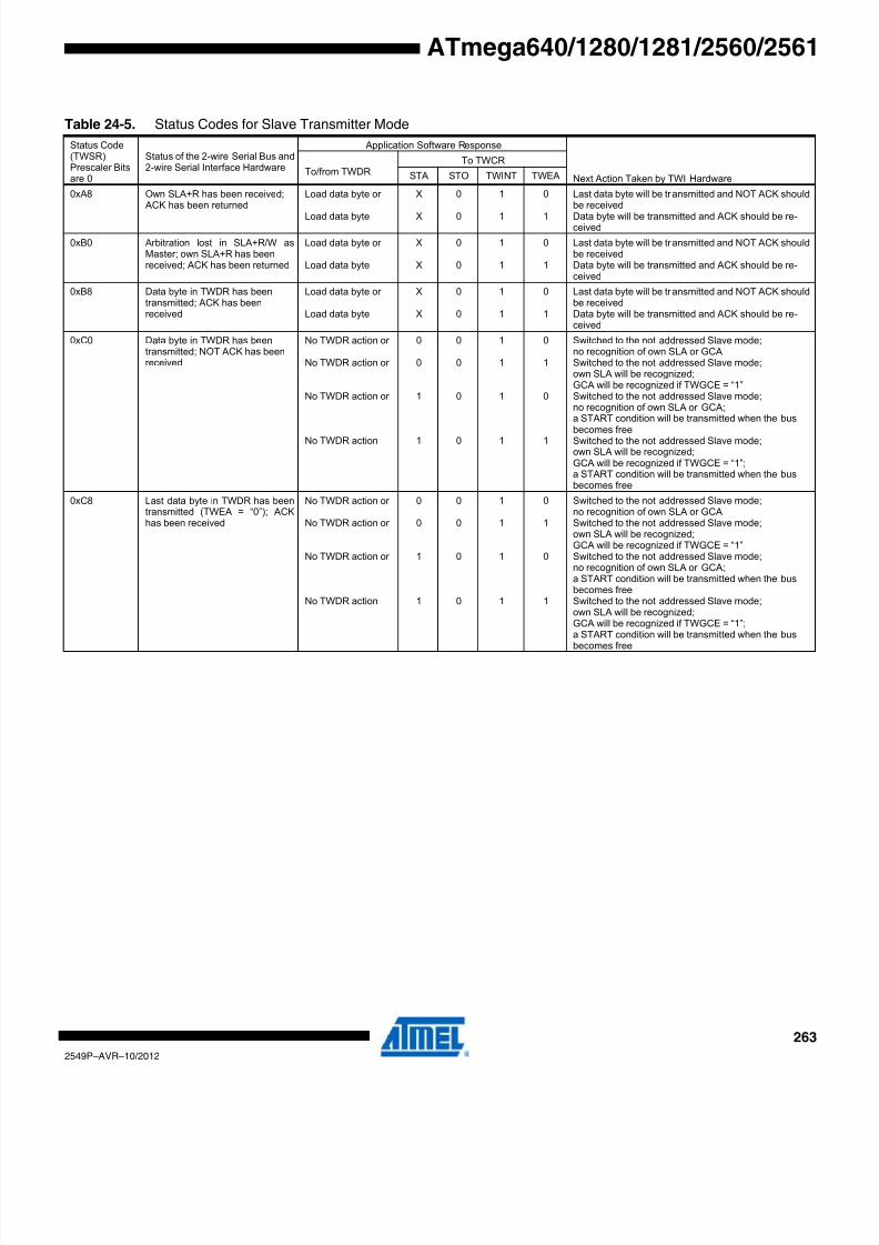
8/20/2019 At Mega 1281 Unlocked
http://slidepdf.com/reader/full/at-mega-1281-unlocked 263/446
263
2549P–AVR–10/2012
ATmega640/1280/1281/2560/2561
Table 24-5. Status Codes for Slave Transmitter Mode
Status Code(TWSR)Prescaler Bitsare 0
Status of the 2-wire Serial Bus and2-wire Serial Interface Hardware
Application Software Response
Next Action Taken by TWI HardwareTo/from TWDR
To TWCR
STA STO TWINT TWEA
0xA8 Own SLA+R has been received; ACK has been returned
Load data byte or
Load data byte
X
X
0
0
1
1
0
1
Last data byte will be transmitted and NOT ACK shouldbe receivedData byte will be transmitted and ACK should be re-ceived
0xB0 Arbitration lost in SLA+R/W asMaster; own SLA+R has beenreceived; ACK has been returned
Load data byte or
Load data byte
X
X
0
0
1
1
0
1
Last data byte will be transmitted and NOT ACK shouldbe receivedData byte will be transmitted and ACK should be re-ceived
0xB8 Data byte in TWDR has beentransmitted; ACK has beenreceived
Load data byte or
Load data byte
X
X
0
0
1
1
0
1
Last data byte will be transmitted and NOT ACK shouldbe receivedData byte will be transmitted and ACK should be re-ceived
0xC0 Data byte in TWDR has beentransmitted; NOT ACK has beenreceived
No TWDR action or
No TWDR action or
No TWDR action or
No TWDR action
0
0
1
1
0
0
0
0
1
1
1
1
0
1
0
1
Switched to the not addressed Slave mode;no recognition of own SLA or GCASwitched to the not addressed Slave mode;own SLA will be recognized;GCA will be recognized if TWGCE = “1”Switched to the not addressed Slave mode;no recognition of own SLA or GCA;a START condition will be transmitted when the busbecomes freeSwitched to the not addressed Slave mode;own SLA will be recognized;GCA will be recognized if TWGCE = “1”;a START condition will be transmitted when the busbecomes free
0xC8 Last data byte in TWDR has beentransmitted (TWEA = “0”); ACKhas been received
No TWDR action or
No TWDR action or
No TWDR action or
No TWDR action
0
0
1
1
0
0
0
0
1
1
1
1
0
1
0
1
Switched to the not addressed Slave mode;no recognition of own SLA or GCASwitched to the not addressed Slave mode;own SLA will be recognized;GCA will be recognized if TWGCE = “1”Switched to the not addressed Slave mode;no recognition of own SLA or GCA;a START condition will be transmitted when the busbecomes freeSwitched to the not addressed Slave mode;own SLA will be recognized;GCA will be recognized if TWGCE = “1”;
a START condition will be transmitted when the busbecomes free

8/20/2019 At Mega 1281 Unlocked
http://slidepdf.com/reader/full/at-mega-1281-unlocked 264/446
264
2549P–AVR–10/2012
ATmega640/1280/1281/2560/2561
Figure 24-18. Formats and States in the Slave Transmitter Mode
24.7.5 Miscellaneous States
There are two status codes that do not correspond to a defined TWI state, see Table 24-6.
Status 0xF8 indicates that no relevant information is available because the T WINT Flag is no
set. This occurs between other states, and when the TWI is not involved in a serial transfer.
Status 0x00 indicates that a bus error has occurred during a 2-wire Serial Bus transfer. A bus
error occurs when a START or STOP condition occurs at an illegal position in the format frame
Examples of such illegal positions are during the serial transfer of an address byte, a data byte
or an acknowledge bit. When a bus error occurs, TWINT is set. To recover from a bus error, the
TWSTO Flag must set and TWINT must be cleared by writing a logic one to it. This causes the
TWI to enter the not addressed Slave mode and to clear the TWSTO Flag (no other bits in
TWCR are affected). The SDA and SCL lines are released, and no STOP condition istransmitted.
24.7.6 Combining Several TWI Modes
In some cases, several TWI modes must be combined in order to complete the desired actionConsider for example reading data from a serial EEPROM. Typically, such a transfer involves
the following steps:
1. The transfer must be initiated.
2. The EEPROM must be instructed what location should be read.
3. The reading must be performed.
4. The transfer must be finished.
S SLA R A DATA A
$A8 $B8
A
$B0
Reception of the ownslave address and one ormore data bytes
Last data byte transmitted.Switched to not addressedslave (TWEA = '0')
Arbitration lost as masterand addressed as slave
n
From master to slave
From slave to master
Any number of data bytesand their associated acknowledge bits
This number (contained in TWSR) correspondsto a defined state of the Two-Wire Serial Bus. Theprescaler bits are zero or masked to zero
P or SDATA
$C0
DATA A
A
$C8
P or SAll 1's
A
Table 24-6. Miscellaneous States
Status Code(TWSR)Prescaler Bitsare 0
Status of the 2-wire Serial Busand 2-wire Serial Interface Hard-ware
Application Software Response
Next Action Taken by TWI HardwareTo/from TWDR
To TWCR
STA STO TWINT TWEA
0xF8 No relevant state informationavailable; TWINT = “0”
No TWDR action No TWCR action Wait or proceed current transfer
0x00 Bus error due to an illegalSTART or STOP condition
No TWDR action 0 1 1 X Only the internal hardware is affected, no STOP condi-tion is sent on the bus. In all cases, the bus is releasedand TWSTO is cleared.

8/20/2019 At Mega 1281 Unlocked
http://slidepdf.com/reader/full/at-mega-1281-unlocked 265/446
265
2549P–AVR–10/2012
ATmega640/1280/1281/2560/2561
Note that data is transmitted both from Master to Slave and vice versa. The Master must instruc
the Slave what location it wants to read, requiring the use of the MT mode. Subsequently, data
must be read from the Slave, implying the use of the MR mode. Thus, the transfer direction mus
be changed. The Master must keep control of the bus during all these steps, and the steps
should be carried out as an atomical operation. If this principle is violated in a multimaster sys-
tem, another Master can alter the data pointer in the EEPROM between steps 2 and 3, and the
Master will read the wrong data location. Such a change in transfer direction is accomplished bytransmitting a REPEATED START between the transmission of the address byte and reception
of the data. After a REPEATED START, the Master keeps ownership of the bus. The following
figure shows the flow in this transfer.
Figure 24-19. Combining Several TWI Modes to Access a Serial EEPROM
24.8 Multi-master Systems and Arbitration
If multiple masters are connected to the same bus, transmissions may be initiated simultane
ously by one or more of them. The TWI standard ensures that such situations are handled in
such a way that one of the masters will be allowed to proceed with the transfer, and that no data
will be lost in the process. An example of an arbitration situation is depicted below, where two
masters are trying to transmit data to a Slave Receiver.
Figure 24-20. An Arbitration Example
Several different scenarios may arise during arbitration, as described below:
• Two or more masters are performing identical communication with the same Slave. In thiscase, neither the Slave nor any of the masters will know about the bus contention.
• Two or more masters are accessing the same Slave with different data or direction bit. In thiscase, arbitration will occur, either in the READ/ WRITE bit or in the data bits. The masterstrying to output a one on SDA while another Master outputs a zero will lose the arbitration.Losing masters will switch to not addressed Slave mode or wait until the bus is free andtransmit a new START condition, depending on application software action.
Master Transmitter Master Receiver
S = START Rs = REPEATED START P = STOP
Transmitted from master to slave Transmitted from slave to master
S SLA+W A ADDRESS A Rs SLA+R A DATA A P
Device 1MASTER
TRANSMITTER
Device 2MASTER
TRANSMITTER
Device 3SLAVE
RECEIVER
Device n
SDA
SCL
........ R1 R2
VCC

8/20/2019 At Mega 1281 Unlocked
http://slidepdf.com/reader/full/at-mega-1281-unlocked 266/446
266
2549P–AVR–10/2012
ATmega640/1280/1281/2560/2561
• Two or more masters are accessing different slaves. In this case, arbitration will occur in theSLA bits. Masters trying to output a one on SDA while another Master outputs a zero willlose the arbitration. Masters losing arbitration in SLA will switch to Slave mode to check ifthey are being addressed by the winning Master. If addressed, they will switch to SR or STmode, depending on the value of the READ/ WRITE bit. If they are not being addressed, theywill switch to not addressed Slave mode or wait until the bus is free and transmit a new
START condition, depending on application software action.This is summarized in Figure 24-21. Possible status values are given in circles.
Figure 24-21. Possible Status Codes Caused by Arbitration
24.9 Register Description
24.9.1 TWBR – TWI Bit Rate Register
• Bits 7:0 – TWI Bit Rate Register
TWBR selects the division factor for the bit rate generator. The bit rate generator is a frequency
divider which generates the SCL clock frequency in the Master modes. See “Bit Rate Generato
Unit” on page 247 for calculating bit rates.
24.9.2 TWCR – TWI Control Register
The TWCR is used to control the operation of the TWI. It is used to enable the TWI, to initiate a
Master access by applying a START condition to the bus, to generate a Receiver acknowledge
to generate a stop condition, and to control halting of the bus while the data to be written to the
bus are written to the TWDR. It also indicates a write collision if data is attempted written to
TWDR while the register is inaccessible.
OwnAddress / General Call
received
Arbitration lost in SLA
TWI bus will be released and not addressed slave mode will be enteredA START condition will be transmitted when the bus becomes free
No
Arbitration lost in Data
Direction
Yes
Write Data byte will be received and NOT ACK will be returnedData byte will be received and ACK will be returned
Last data byte will be transmitted and NOT ACK should be receivedData byte will be transmitted and ACK should be received
ReadB0
68/78
38
SLASTART Data STOP
Bit 7 6 5 4 3 2 1 0
(0xB8) TWBR7 TWBR6 TWBR5 TWBR4 TWBR3 TWBR2 TWBR1 TWBR0 TWBR
Read/Write R/W R/W R/W R/W R/W R/W R/W R/W
Initial Value 0 0 0 0 0 0 0 0
Bit 7 6 5 4 3 2 1 0
(0xBC) TWINT TWEA TWSTA TWSTO TWWC TWEN – TWIE TWCR
Read/Write R/W R/W R/W R/W R R/W R R/W
Initial Value 0 0 0 0 0 0 0 0

8/20/2019 At Mega 1281 Unlocked
http://slidepdf.com/reader/full/at-mega-1281-unlocked 267/446
267
2549P–AVR–10/2012
ATmega640/1280/1281/2560/2561
• Bit 7 – TWINT: TWI Interrupt Flag
This bit is set by hardware when the TWI has finished its current job and expects application
software response. If the I-bit in SREG and TWIE in TWCR are set, the MCU will jump to the
TWI Interrupt Vector. While the TWINT Flag is set, the SCL low period is stretched. The TWINT
Flag must be cleared by software by writing a logic one to it. Note that this flag is not automati
cally cleared by hardware when executing the interrupt routine. Also note that clearing this flag
starts the operation of the TWI, so all accesses to the TWI Address Register (TWAR), TWI Status Register (TWSR), and TWI Data Register (TWDR) must be complete before clearing this
flag.
• Bit 6 – TWEA: TWI Enable Acknowledge Bit
The TWEA bit controls the generation of the acknowledge pulse. If the TWEA bit is written to
one, the ACK pulse is generated on the TWI bus if the following conditions are met:
1. The device’s own slave address has been received.
2. A general call has been received, while the TWGCE bit in the TWAR is set.
3. A data byte has been received in Master Receiver or Slave Receiver mode.
By writing the TWEA bit to zero, the device can be virtually disconnected from the 2-wire Seria
Bus temporarily. Address recognition can then be resumed by writing the TWEA bit to one
again.
• Bit 5 – TWSTA: TWI START Condition Bit
The application writes the TWSTA bit to one when it desires to become a Master on the 2-wire
Serial Bus. The TWI hardware checks if the bus is available, and generates a START condition
on the bus if it is free. However, if the bus is not free, the T WI waits until a STOP condition is
detected, and then generates a new START condition to claim the bus Master status. TWSTA
must be cleared by software when the START condition has been transmitted.
• Bit 4 – TWSTO: TWI STOP Condition Bit
Writing the TWSTO bit to one in Master mode will generate a STOP condition on the 2-wireSerial Bus. When the STOP condition is executed on the bus, the T WSTO bit is cleared auto
matically. In Slave mode, setting the TWSTO bit can be used to recover from an error condition
This will not generate a STOP condition, but the TWI returns to a well-defined unaddressed
Slave mode and releases the SCL and SDA lines to a high impedance state.
• Bit 3 – TWWC: TWI Write Collision Flag
The TWWC bit is set when attempting to write to the TWI Data Register – TWDR when TWINT is
low. This flag is cleared by writing the TWDR Register when TWINT is high.
• Bit 2 – TWEN: TWI Enable Bit
The TWEN bit enables TWI operation and activates the TWI interface. When TWEN is written to
one, the TWI takes control over the I/O pins connected to the SCL and SDA pins, enabling theslew-rate limiters and spike filters. If this bit is written to zero, the TWI is switched off and all TW
transmissions are terminated, regardless of any ongoing operation.
• Bit 1 – Res: Reserved Bit
This bit is a reserved bit and will always read as zero.

8/20/2019 At Mega 1281 Unlocked
http://slidepdf.com/reader/full/at-mega-1281-unlocked 268/446
268
2549P–AVR–10/2012
ATmega640/1280/1281/2560/2561
• Bit 0 – TWIE: TWI Interrupt Enable
When this bit is written to one, and the I-bit in SREG is set, the TWI interrupt request will be acti
vated for as long as the TWINT Flag is high.
24.9.3 TWSR – TWI Status Register
• Bits 7:3 – TWS: TWI Status
These five bits reflect the status of the TWI logic and the 2-wire Serial Bus. The different status
codes are described later in this section. Note that the value read from TWSR contains both the
5-bit status value and the 2-bit prescaler value. The application designer should mask the pres-
caler bits to zero when checking the Status bits. This makes status checking independent of
prescaler setting. This approach is used in this datasheet, unless otherwise noted.
• Bit 2 – Res: Reserved BitThis bit is reserved and will always read as zero.
• Bits 1:0 – TWPS: TWI Prescaler Bits
These bits can be read and written, and control the bit rate prescaler.
To calculate bit rates, see “Bit Rate Generator Unit” on page 247. The value of TWPS1:0 is used
in the equation.
24.9.4 TWDR – TWI Data Register
In Transmit mode, TWDR contains the next byte to be transmitted. In Receive mode, the TWDR
contains the last byte received. It is writable while the TWI is not in the process of shifting a byteThis occurs when the TWI Interrupt Flag (TWINT) is set by hardware. Note that the Data Regis-
ter cannot be initialized by the user before the first interrupt occurs. The data in TWDR remains
stable as long as TWINT is set. While data is shifted out, data on the bus is simultaneously
shifted in. TWDR always contains the last byte present on the bus, except after a wake up from
a sleep mode by the TWI interrupt. In this case, the contents of TWDR is undefined. In the case
of a lost bus arbitration, no data is lost in the transition from Master to Slave. Handling of the
ACK bit is controlled automatically by the TWI logic, the CPU cannot access the ACK bit directly
Bit 7 6 5 4 3 2 1 0(0xB9) TWS7 TWS6 TWS5 TWS4 TWS3 – TWPS1 TWPS0 TWSR
Read/Write R R R R R R R/W R/W
Initial Value 1 1 1 1 1 0 0 0
Table 24-7. TWI Bit Rate Prescaler
TWPS1 TWPS0 Prescaler Value
0 0 1
0 1 4
1 0 16
1 1 64
Bit 7 6 5 4 3 2 1 0
(0xBB) TWD7 TWD6 TWD5 TWD4 TWD3 TWD2 TWD1 TWD0 TWDR
Read/Write R/W R/W R/W R/W R/W R/W R/W R/W
Initial Value 1 1 1 1 1 1 1 1

8/20/2019 At Mega 1281 Unlocked
http://slidepdf.com/reader/full/at-mega-1281-unlocked 269/446
269
2549P–AVR–10/2012
ATmega640/1280/1281/2560/2561
• Bits 7:0 – TWD: TWI Data Register
These eight bits constitute the next data byte to be transmitted, or the latest data byte received
on the 2-wire Serial Bus.
24.9.5 TWAR – TWI (Slave) Address Register
The TWAR should be loaded with the 7-bit Slave address (in the seven most significant bits of
TWAR) to which the TWI will respond when programmed as a Slave Transmitter or Receiver
and not needed in the Master modes. In multimaster systems, TWAR must be set in masters
which can be addressed as Slaves by other Masters.
The LSB of TWAR is used to enable recognition of the general call address (0x00). There is an
associated address comparator that looks for the slave address (or general call address if
enabled) in the received serial address. If a match is found, an interrupt request is generated.
• Bits 7:1 – TWA: TWI (Slave) Address Register
These seven bits constitute the slave address of the TWI unit.
• Bit 0 – TWGCE: TWI General Call Recognition Enable Bit
If set, this bit enables the recognition of a General Call given over the 2-wire Serial Bus.
24.9.6 TWAMR – TWI (Slave) Address Mask Register
• Bits 7:1 – TWAM: TWI Address Mask
The TWAMR can be loaded with a 7-bit Slave Address mask. Each of the bits in TWAMR can
mask (disable) the corresponding address bit in the TWI Address Register (TWAR). If the mask
bit is set to one then the address match logic ignores the compare between the incoming
address bit and the corresponding bit in TWAR. Figure 24-22 shows the address match logic in
detail.
Figure 24-22. TWI Address Match Logic, Block Diagram
Bit 7 6 5 4 3 2 1 0(0xBA) TWA6 TWA5 TWA4 TWA3 TWA2 TWA1 TWA0 TWGCE TWAR
Read/Write R/W R/W R/W R/W R/W R/W R/W R/W
Initial Value 1 1 1 1 1 1 1 0
Bit 7 6 5 4 3 2 1 0
(0xBD) TWAM[6:0] – TWAMR
Read/Write R/W R/W R/W R/W R/W R/W R/W R
Initial Value 0 0 0 0 0 0 0 0
AddressMatch
Address Bit Comparator 0
Address Bit Comparator 6..1
TWAR0
TWAMR0
AddressBit 0

8/20/2019 At Mega 1281 Unlocked
http://slidepdf.com/reader/full/at-mega-1281-unlocked 270/446
270
2549P–AVR–10/2012
ATmega640/1280/1281/2560/2561
• Bit 0 – Res: Reserved Bit
This bit is reserved and will always read as zero.

8/20/2019 At Mega 1281 Unlocked
http://slidepdf.com/reader/full/at-mega-1281-unlocked 271/446
271
2549P–AVR–10/2012
ATmega640/1280/1281/2560/2561
25. AC – Analog ComparatorThe Analog Comparator compares the input values on the positive pin AIN0 and negative pin
AIN1. When the voltage on the positive pin AIN0 is higher than the voltage on the negative pin
AIN1, the Analog Comparator output, ACO, is set. The comparator’s output can be set to trigge
the Timer/Counter1 Input Capture function. In addition, the comparator can trigger a separate
interrupt, exclusive to the Analog Comparator. The user can select Interrupt triggering on com
parator output rise, fall or toggle. A block diagram of the comparator and its surrounding logic is
shown in Figure 25-1.
The Power Reduction ADC bit, PRADC, in “PRR0 – Power Reduction Register 0” on page 56
must be disabled by writing a logical zero to be able to use the ADC input MUX.
Figure 25-1. Analog Comparator Block Diagram(2)
Note: 1. See Table 25-1.
2. Refer to Figure 1-1 on page 2 and Table 13-5 on page 79 for Analog Comparator pinplacement.
25.1 Analog Comparator Multiplexed Input
It is possible to select any of the ADC15:0 pins to replace the negative input to the Analog Com
parator. The ADC multiplexer is used to select this input, and consequently, the ADC must be
switched off to utilize this feature. If the Analog Comparator Multiplexer Enable bit (ACME in
ADCSRB) is set and the ADC is switched off (ADEN in ADCSRA is zero), MUX5 and MUX2:0 in
ADMUX select the input pin to replace the negative input to the Analog Comparator, as shown in
Table 25-1. If ACME is cleared or ADEN is set, AIN1 is applied to the negative input to the Ana-
log Comparator.
ACBG
BANDGAPREFERENCE
ADC MULTIPLEXEROUTPUT
ACME
ADEN
(1)
Table 25-1. Analog Comparator Mulitiplexed Input
ACME ADEN MUX5 MUX2:0 Analog Comparator Negative Input
0 x x xxx AIN1
1 1 x xxx AIN1
1 0 0 000 ADC0
1 0 0 001 ADC1
1 0 0 010 ADC2
1 0 0 011 ADC3

8/20/2019 At Mega 1281 Unlocked
http://slidepdf.com/reader/full/at-mega-1281-unlocked 272/446
272
2549P–AVR–10/2012
ATmega640/1280/1281/2560/2561
25.2 Register Description
25.2.1 ADCSRB – ADC Control and Status Register B
• Bit 6 – ACME: Analog Comparator Multiplexer Enable
When this bit is written logic one and the ADC is switched off (ADE N in ADCSRA is zero), the
ADC multiplexer selects the negative input to the Analog Comparator.W
hen this bit is writtenlogic zero, AIN1 is applied to the negative input of the Analog Comparator. For a detailed
description of this bit, see “Analog Comparator Multiplexed Input” on page 271.
25.2.2 ACSR – Analog Comparator Control and Status Register
• Bit 7 – ACD: Analog Comparator Disable
When this bit is written logic one, the power to the Analog Comparator is switched off. This bit
can be set at any time to turn off the Analog Comparator. This will reduce power consumption inActive and Idle mode. When changing the ACD bit, the Analog Comparator Interrupt must be
disabled by clearing the ACIE bit in ACSR. Otherwise an interrupt can occur when the bit is
changed.
1 0 0 100 ADC4
1 0 0 101 ADC5
1 0 0 110 ADC6
1 0 0 111 ADC7
1 0 1 000 ADC8
1 0 1 001 ADC9
1 0 1 010 ADC10
1 0 1 011 ADC11
1 0 1 100 ADC12
1 0 1 101 ADC13
1 0 1 110 ADC14
1 0 1 111 ADC15
Table 25-1. Analog Comparator Mulitiplexed Input (Continued)
ACME ADEN MUX5 MUX2:0 Analog Comparator Negative Input
Bit 7 6 5 4 3 2 1 0
(0x7B) – ACME – – MUX5 ADTS2 ADTS1 ADTS0 ADCSRB
Read/ Write R R/ W R R R/ W R/ W R/ W R/ W
Initial Value 0 0 0 0 0 0 0 0
Bit 7 6 5 4 3 2 1 0
0x30 (0x50) ACD ACBG ACO ACI ACIE ACIC ACIS1 ACIS0 ACSR
Read/ Write R/ W R/ W R R/ W R/ W R/ W R/ W R/ W
Initial Value 0 0 N /A 0 0 0 0 0
8/20/2019 At Mega 1281 Unlocked
http://slidepdf.com/reader/full/at-mega-1281-unlocked 273/446
273
2549P–AVR–10/2012
ATmega640/1280/1281/2560/2561
• Bit 6 – ACBG: Analog Comparator Bandgap Select
When this bit is set, a fixed bandgap reference voltage replaces the positive input to the Analog
Comparator. When this bit is cleared, AIN0 is applied to the positive input of the Analog Compar
ator. When the bandgap reference is used as input to the Analog Comparator, it will take a
certain time for the voltage to stabilize. If not stabilized, the first conversion may give a wrongvalue. See “Internal Voltage Reference” on page 62.
• Bit 5 – ACO: Analog Comparator Output
The output of the Analog Comparator is synchronized and then directly connected to ACO. The
synchronization introduces a delay of 1 - 2 clock cycles.
• Bit 4 – ACI: Analog Comparator Interrupt Flag
This bit is set by hardware when a comparator output event triggers the interrupt mode defined
by ACIS1 and ACIS0. The Analog Comparator interrupt routine is executed if the ACIE bit is se
and the I-bit in SREG is set. ACI is cleared by hardware when executing the corresponding inter
rupt handling vector. Alternatively, ACI is cleared by writing a logic one to the flag.
• Bit 3 – ACIE: Analog Comparator Interrupt Enable
When the ACIE bit is written logic one and the I-bit in the Status Register is set, the Analog Com
parator interrupt is activated. When written logic zero, the interrupt is disabled.
• Bit 2 – ACIC: Analog Comparator Input Capture Enable
When written logic one, this bit enables the input capture function in Timer/Counter1 to be trig-
gered by the Analog Comparator. The comparator output is in this case directly connected to the
input capture front-end logic, making the comparator utilize the noise canceler and edge selec
features of the Timer/Counter1 Input Capture interrupt. When written logic zero, no connection
between the Analog Comparator and the input capture function exists. To make the comparato
trigger the Timer/Counter1 Input Capture interrupt, the ICIE1 bit in the Timer Interrupt Mask
Register (TIMSK1) must be set.
• Bits 1, 0 – ACIS1, ACIS0: Analog Comparator Interrupt Mode Select
These bits determine which comparator events that trigger the Analog Comparator interrupt. The
different settings are shown in Table 25-2.
When changing the ACIS1/ACIS0 bits, the Analog Comparator Interrupt must be disabled by
clearing its Interrupt Enable bit in the ACSR Register. Otherwise an interrupt can occur when the
bits are changed.
Table 25-2. ACIS1/ACIS0 Settings
ACIS1 ACIS0 Interrupt Mode
0 0 Comparator Interrupt on Output Toggle
0 1 Reserved
1 0 Comparator Interrupt on Falling Output Edge1 1 Comparator Interrupt on Rising Output Edge

8/20/2019 At Mega 1281 Unlocked
http://slidepdf.com/reader/full/at-mega-1281-unlocked 274/446
274
2549P–AVR–10/2012
ATmega640/1280/1281/2560/2561
25.2.3 DIDR1 – Digital Input Disable Register 1
• Bit 1, 0 – AIN1D, AIN0D: AIN1, AIN0 Digital Input DisableWhen this bit is written logic one, the digital input buffer on the AIN1/0 pin is disabled. The corre
sponding PIN Register bit will always read as zero when this bit is set. When an analog signal is
applied to the AIN1/0 pin and the digital input from this pin is not needed, this bit should be writ
ten logic one to reduce power consumption in the digital input buffer.
Bit 7 6 5 4 3 2 1 0
(0x7F) – – – – – – AIN1D AIN0D DIDR1
Read/ Write R R R R R R R/ W R/ W
Initial Value 0 0 0 0 0 0 0 0
8/20/2019 At Mega 1281 Unlocked
http://slidepdf.com/reader/full/at-mega-1281-unlocked 275/446
275
2549P–AVR–10/2012
ATmega640/1280/1281/2560/2561
26. ADC – Analog to Digital Converter
26.1 Features
• 10-bit Resolution• 1 LSB Integral Non-linearity
• ±2 LSB Absolute Accuracy
• 13µs - 260µs Conversion Time
• Up to 76.9kSPS (Up to 15kSPS at Maximum Resolution)
• 16 Multiplexed Single Ended Input Channels
• 14 Differential input channels
• 4 Differential Input Channels with Optional Gain of 10× and 200×
• Optional Left Adjustment for ADC Result Readout
• 0V - VCC ADC Input Voltage Range
• 2.7V - VCC Differential ADC Voltage Range
• Selectable 2.56V or 1.1V ADC Reference Voltage
• Free Running or Single Conversion Mode• Interrupt on ADC Conversion Complete
• Sleep Mode Noise Canceler
The ATmega640/1280/1281/2560/2561 features a 10-bit successive approximation ADC. The
ADC is connected to an 8/16-channel Analog Multiplexer which allows eight/sixteen single
ended voltage inputs constructed from the pins of Port F and Port K. The single-ended voltage
inputs refer to 0V (GND).
The device also supports 16/32 differential voltage input combinations. Four of the differentia
inputs (ADC1 & ADC0, ADC3 & ADC2, ADC9 & ADC8 and ADC11 & ADC10) are equipped with
a programmable gain stage, providing amplification steps of 0 dB (1×), 20 dB (10×) or 46 dB
(200×) on the differential input voltage before the ADC conversion. The 16 channels are split in
two sections of 8 channels where in each section seven differential analog input channels sharea common negative terminal (ADC1/ADC9), while any other ADC input in that section can be
selected as the positive input terminal. If 1× or 10× gain is used, 8 bit resolution can be
expected. If 200× gain is used, 7 bit resolution can be expected.
The ADC contains a Sample and Hold circuit which ensures that the input voltage to the ADC is
held at a constant level during conversion. A block diagram of the ADC is shown in Figure 26-1
on page 276.
The ADC has a separate analog supply voltage pin, AVCC. AVCC must not differ more than
±0.3V from VCC. See the paragraph “ADC Noise Canceler” on page 283 on how to connect this
pin.
Internal reference voltages of nominally 1.1V, 2.56V or AVCC are provided On-chip. The voltage
reference may be externally decoupled at the AREF pin by a capacitor for better noise
performance.
The Power Reduction ADC bit, PRADC, in “PRR0 – Power Reduction Register 0” on page 56
must be disabled by writing a logical zero to enable the ADC.
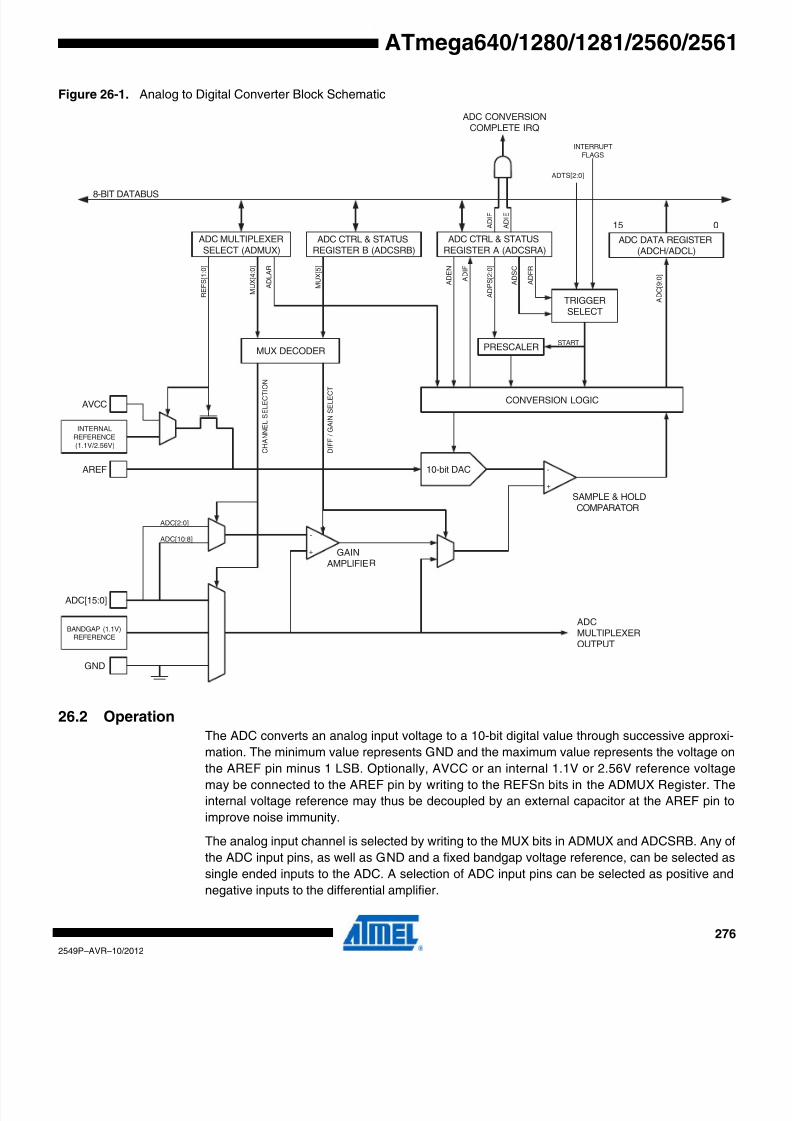
8/20/2019 At Mega 1281 Unlocked
http://slidepdf.com/reader/full/at-mega-1281-unlocked 276/446
276
2549P–AVR–10/2012
ATmega640/1280/1281/2560/2561
Figure 26-1. Analog to Digital Converter Block Schematic
26.2 Operation
The ADC converts an analog input voltage to a 10-bit digital value through successive approxi-
mation. The minimum value represents GND and the maximum value represents the voltage on
the AREF pin minus 1 LSB. Optionally, AVCC or an internal 1.1V or 2.56V reference voltagemay be connected to the AREF pin by writing to the REFSn bits in the ADMUX Register. The
internal voltage reference may thus be decoupled by an external capacitor at the AREF pin to
improve noise immunity.
The analog input channel is selected by writing to the MUX bits in ADMUX and ADCSRB. Any o
the ADC input pins, as well as GND and a fixed bandgap voltage reference, can be selected as
single ended inputs to the ADC. A selection of ADC input pins can be selected as positive and
negative inputs to the differential amplifier.
ADC CONVERSION
COMPLETE IRQ
8-BIT DATABUS
15 0ADIE
ADFR
ADSC
ADEN
ADIF
ADIF
MUX[4:0]
ADPS[2:0]
SAMPLE & HOLD
COMPARATOR
INTERNAL
REFERENCE
(1.1V/2.56V)
AVCC
REFS[1:0]
ADLAR
CHANNELSELECTION
ADC[9:0]
ADC
MULTIPLEXER
OUTPUT
GAIN
AMPLIFIER
AREF
BANDGAP (1.1V)REFERENCE
GND
CONVERSION LOGIC
ADC CTRL & STATUS
REGISTER B (ADCSRB)
ADC CTRL & STATUS
REGISTER A (ADCSRA)
PRESCALER
ADC MULTIPLEXER
SELECT (ADMUX)
MUX DECODER
DIFF/GAIN
SELECT
ADC DATA REGISTER
(ADCH/ADCL)
ADC[2:0]
TRIGGER
SELECT
START
INTERRUPT
FLAGS
ADTS[2:0]
+
-
ADC[15:0]
+
-10-bit DAC
MUX[5]
ADC[10:8]

8/20/2019 At Mega 1281 Unlocked
http://slidepdf.com/reader/full/at-mega-1281-unlocked 277/446
277
2549P–AVR–10/2012
ATmega640/1280/1281/2560/2561
If differential channels are selected, the voltage difference between the selected input channe
pair then becomes the analog input to the ADC. If single ended channels are used, the amplifie
is bypassed altogether.
The ADC is enabled by setting the ADC Enable bit, ADEN in ADCSRA. Voltage reference and
input channel selections will not go into effect until ADEN is set. The ADC does not consume
power when ADEN is cleared, so it is recommended to switch off the ADC before entering powe
saving sleep modes.
The ADC generates a 10-bit result which is presented in the ADC Data Registers, ADCH and
ADCL. By default, the result is presented right adjusted, but can optionally be presented lef
adjusted by setting the ADLAR bit in ADMUX.
If the result is left adjusted and no more than 8-bit precision is required, it is sufficient to read
ADCH. Otherwise, ADCL must be read first, then ADCH, to ensure that the content of the Data
Registers belongs to the same conversion. Once ADCL is read, ADC access to Data Registers
is blocked. This means that if ADCL has been read, and a conversion completes before ADCH is
read, neither register is updated and the result from the conversion is lost. When ADCH is read
ADC access to the ADCH and ADCL Registers is re-enabled.
The ADC has its own interrupt which can be triggered when a conversion completes. When ADCaccess to the Data Registers is prohibited between reading of ADCH and ADCL, the interrup
will trigger even if the result is lost.
26.3 Starting a Conversion
A single conversion is started by writing a logical one to the ADC Start Conversion bit, ADSC
This bit stays high as long as the conversion is in progress and will be cleared by hardware
when the conversion is completed. If a different data channel is selected while a conversion is in
progress, the ADC will finish the current conversion before performing the channel change.
Alternatively, a conversion can be triggered automatically by various sources. Auto Triggering is
enabled by setting the ADC Auto Trigger Enable bit, ADATE in ADCSRA. The trigger source is
selected by setting the ADC Trigger Select bits, ADTS in ADCSRB (see description of the ADTSbits for a list of the trigger sources). When a positive edge occurs on the selected trigger signal
the ADC prescaler is reset and a conversion is started. This provides a method of starting con-
versions at fixed intervals. If the trigger signal still is set when the conversion completes, a new
conversion will not be started. If another positive edge occurs on the trigger signal during con-
version, the edge will be ignored. Note that an Interrupt Flag will be set even if the specific
interrupt is disabled or the Global Interrupt Enable bit in SREG is cleared. A conversion can thus
be triggered without causing an interrupt. However, the Interrupt Flag must be cleared in order to
trigger a new conversion at the next interrupt event.

8/20/2019 At Mega 1281 Unlocked
http://slidepdf.com/reader/full/at-mega-1281-unlocked 278/446
278
2549P–AVR–10/2012
ATmega640/1280/1281/2560/2561
Figure 26-2. ADC Auto Trigger Logic
Using the ADC Interrupt Flag as a trigger source makes the ADC start a new conversion as soon
as the ongoing conversion has finished. The ADC then operates in Free Running mode, con-
stantly sampling and updating the ADC Data Register. The first conversion must be started bywriting a logical one to the ADSC bit in ADCSRA. In this mode the ADC will perform successive
conversions independently of whether the ADC Interrupt Flag, ADIF is cleared or not.
If Auto Triggering is enabled, single conversions can be started by writing ADSC in ADCSRA to
one. ADSC can also be used to determine if a conversion is in progress. The ADSC bit will be
read as one during a conversion, independently of how the conversion was started.
26.4 Prescaling and Conversion Timing
Figure 26-3. ADC Prescaler
By default, the successive approximation circuitry requires an input clock frequency between
50kHz and 200kHz. If a lower resolution than 10 bits is needed, the input clock frequency to the
ADC can be as high as 1000kHz to get a higher sample rate.
The ADC module contains a prescaler, which generates an acceptable ADC clock frequency
from any CPU frequency above 100kHz. The prescaling is set by the ADPS bits in ADCSRA
ADSC
ADIF
SOURCE 1
SOURCE n
ADTS[2:0]
CONVERSIONLOGIC
PRESCALER
START CLKADC
.
.
.
. EDGEDETECTOR
ADATE
7-BIT ADC PRESCALER
ADC CLOCK SOURCE
CK
ADPS0
ADPS1
ADPS2
C K / 1 2 8
C K / 2
C K / 4
C K / 8
C K / 1 6
C K / 3 2
C K / 6 4
ResetADEN
START
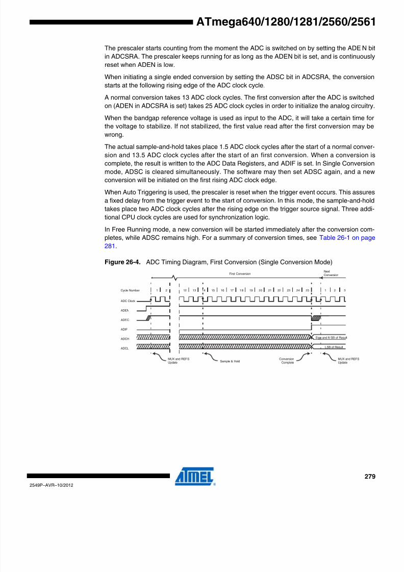
8/20/2019 At Mega 1281 Unlocked
http://slidepdf.com/reader/full/at-mega-1281-unlocked 279/446
279
2549P–AVR–10/2012
ATmega640/1280/1281/2560/2561
The prescaler starts counting from the moment the ADC is switched on by setting the ADEN bi
in ADCSRA. The prescaler keeps running for as long as the ADEN bit is set, and is continuously
reset when ADEN is low.
When initiating a single ended conversion by setting the ADSC bit in ADCSRA, the conversion
starts at the following rising edge of the ADC clock cycle.
A normal conversion takes 13 ADC clock cycles. The first conversion after the ADC is switchedon (ADEN in ADCSRA is set) takes 25 ADC clock cycles in order to initialize the analog circuitry
When the bandgap reference voltage is used as input to the ADC, it will take a certain time for
the voltage to stabilize. If not stabilized, the first value read after the first conversion may be
wrong.
The actual sample-and-hold takes place 1.5 ADC clock cycles after the start of a normal conver
sion and 13.5 ADC clock cycles after the start of an first conversion. When a conversion is
complete, the result is written to the ADC Data Registers, and ADIF is set. In Single Conversion
mode, ADSC is cleared simultaneously. The software may then set ADSC again, and a new
conversion will be initiated on the first rising ADC clock edge.
W
hen Auto Triggering is used, the prescaler is reset when the trigger event occurs. This assuresa fixed delay from the trigger event to the start of conversion. In this mode, the sample-and-hold
takes place two ADC clock cycles after the rising edge on the trigger source signal. Three addi-
tional CPU clock cycles are used for synchronization logic.
In Free Running mode, a new conversion will be started immediately after the conversion com-
pletes, while ADSC remains high. For a summary of conversion times, see Table 26-1 on page
281.
Figure 26-4. ADC Timing Diagram, First Conversion (Single Conversion Mode)
Sign and MSB of Result
LSB of Result
ADC Clock
ADSC
Sample & Hold
ADIF
ADCH
ADCL
Cycle Number
ADEN
1 2 12 13 14 15 16 17 18 19 20 21 22 23 24 25 1 2
First ConversionNextConversion
3
MUX and REFS
UpdateMUX and REFS
UpdateConversion
Complete

8/20/2019 At Mega 1281 Unlocked
http://slidepdf.com/reader/full/at-mega-1281-unlocked 280/446
280
2549P–AVR–10/2012
ATmega640/1280/1281/2560/2561
Figure 26-5. ADC Timing Diagram, Single Conversion
Figure 26-6. ADC Timing Diagram, Auto Triggered Conversion
Figure 26-7. ADC Timing Diagram, Free Running Conversion
1 2 3 4 5 6 7 8 9 10 11 12 13
Sign and MSB of Result
LSB of Result
ADC Clock
ADSC
ADIF
ADCH
ADCL
Cycle Number 1 2
One Conversion Next Conversion
3
Sample & Hold
MUX and REFS
Update
Conversion
CompleteMUX and REFS
Update
1 2 3 4 5 6 7 8 9 10 11 12 13
Sign and MSB of Result
LSB of Result
ADC Clock
Trigger
Source
ADIF
ADCH
ADCL
Cycle Number 1 2
One Conversion Next Conversion
Conversion
CompletePrescaler
Reset
ADATE
Prescaler
Reset
Sample &
Hold
MUX and REFS
Update
11 12 13
Sign and MSB of Result
LSB of Result
ADC Clock
ADSC
ADIF
ADCH
ADCL
Cycle Number1 2
One Conversion Next Conversion
3 4
ConversionComplete
Sample & Hold
MUX and REFS
Update
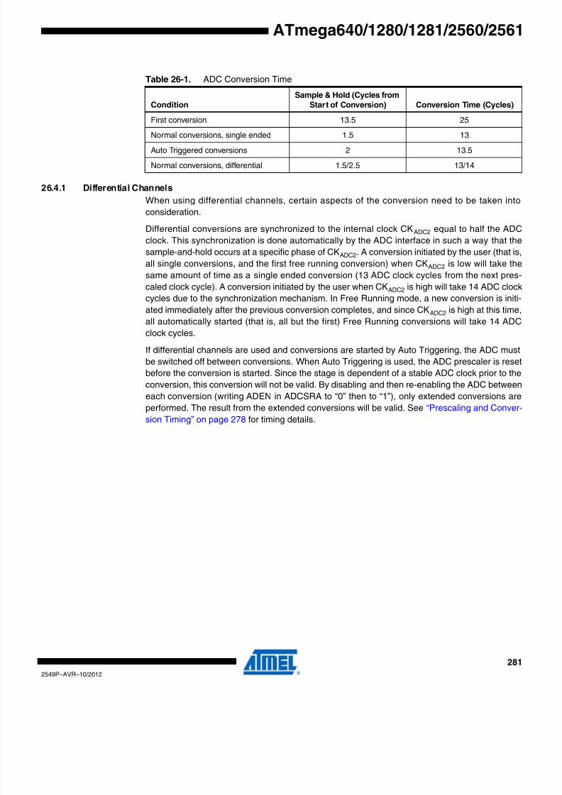
8/20/2019 At Mega 1281 Unlocked
http://slidepdf.com/reader/full/at-mega-1281-unlocked 281/446
281
2549P–AVR–10/2012
ATmega640/1280/1281/2560/2561
26.4.1 Differential Channels
When using differential channels, certain aspects of the conversion need to be taken into
consideration.
Differential conversions are synchronized to the internal clock CKADC2 equal to half the ADC
clock. This synchronization is done automatically by the ADC interface in such a way that the
sample-and-hold occurs at a specific phase of CKADC2. A conversion initiated by the user (that is
all single conversions, and the first free running conversion) when CKADC2 is low will take the
same amount of time as a single ended conversion (13 ADC clock cycles from the next prescaled clock cycle). A conversion initiated by the user when CKADC2 is high will take 14 ADC clock
cycles due to the synchronization mechanism. In Free Running mode, a new conversion is initi-
ated immediately after the previous conversion completes, and since CKADC2 is high at this time
all automatically started (that is, all but the first) Free Running conversions will take 14 ADC
clock cycles.
If differential channels are used and conversions are started by Auto Triggering, the ADC must
be switched off between conversions. When Auto Triggering is used, the ADC prescaler is rese
before the conversion is started. Since the stage is dependent of a stable ADC clock prior to the
conversion, this conversion will not be valid. By disabling and then re-enabling the ADC between
each conversion (writing ADEN in ADCSRA to “0” then to “1”), only extended conversions are
performed. The result from the extended conversions will be valid. See “Prescaling and Conversion Timing” on page 278 for timing details.
Table 26-1. ADC Conversion Time
Condition
Sample & Hold (Cycles from
Start of Conversion) Conversion Time (Cycles)
First conversion 13.5 25
Normal conversions, single ended 1.5 13
Auto Triggered conversions 2 13.5
Normal conversions, differential 1.5/2.5 13/14

8/20/2019 At Mega 1281 Unlocked
http://slidepdf.com/reader/full/at-mega-1281-unlocked 282/446
282
2549P–AVR–10/2012
ATmega640/1280/1281/2560/2561
26.5 Changing Channel or Reference Selection
The MUXn and REFS1:0 bits in the ADMUX Register are single buffered through a temporary
register to which the CPU has random access. This ensures that the channels and reference
selection only takes place at a safe point during the conversion. The channel and reference
selection is continuously updated until a conversion is started. Once the conversion starts, the
channel and reference selection is locked to ensure a sufficient sampling time for the ADC. Con
tinuous updating resumes in the last ADC clock cycle before the conversion completes (ADIF in
ADCSRA is set). Note that the conversion starts on the following rising ADC clock edge afte
ADSC is written. The user is thus advised not to write new channel or reference selection values
to ADMUX until one ADC clock cycle after ADSC is written.
If Auto Triggering is used, the exact time of the triggering event can be indeterministic. Specia
care must be taken when updating the ADMUX Register, in order to control which conversion
will be affected by the new settings.
If both ADATE and ADEN is written to one, an interrupt event can occur at any time. If the
ADMUX Register is changed in this period, the user cannot tell if the next conversion is based
on the old or the new settings. ADMUX can be safely updated in the following ways:
1. When ADATE or ADEN is cleared.
2. During conversion, minimum one ADC clock cycle after the trigger event.
3. After a conversion, before the Interrupt Flag used as trigger source is cleared.
When updating ADMUX in one of these conditions, the new settings will affect the next ADC
conversion.
Special care should be taken when changing differential channels. Once a differential channe
has been selected, the stage may take as much as 125µs to stabilize to the new value. Thus
conversions should not be started within the first 125µs after selecting a new differential chan-
nel. Alternatively, conversion results obtained within this period should be discarded.
The same settling time should be observed for the first differential conversion after changing
ADC reference (by changing the REFS1:0 bits in ADMUX).
26.5.1 ADC Input Channels
When changing channel selections, the user should observe the following guidelines to ensure
that the correct channel is selected:
In Single Conversion mode, always select the channel before starting the conversion. The chan
nel selection may be changed one ADC clock cycle after writing one to ADSC. However, the
simplest method is to wait for the conversion to complete before changing the channel selection
In Free Running mode, always select the channel before starting the first conversion. The chan
nel selection may be changed one ADC clock cycle after writing one to ADSC. However, thesimplest method is to wait for the first conversion to complete, and then change the channel
selection. Since the next conversion has already started automatically, the next result will reflec
the previous channel selection. Subsequent conversions will reflect the new channel selection.
When switching to a differential gain channel, the first conversion result may have a poor accu
racy due to the required settling time for the automatic offset cancellation circuitry. The user
should preferably disregard the first conversion result.

8/20/2019 At Mega 1281 Unlocked
http://slidepdf.com/reader/full/at-mega-1281-unlocked 283/446
283
2549P–AVR–10/2012
ATmega640/1280/1281/2560/2561
26.5.2 ADC Voltage Reference
The reference voltage for the ADC (VREF) indicates the conversion range for the ADC. Single
ended channels that exceed VREF will result in codes close to 0x3FF. VREF can be selected as
either AVCC, internal 1.1V reference, internal 2.56V reference or external AREF pin.
AVCC is connected to the ADC through a passive switch. The internal 1.1V reference is gener
ated from the internal bandgap reference (VBG) through an internal amplifier. In either case, theexternal AREF pin is directly connected to the ADC, and the reference voltage can be made
more immune to noise by connecting a capacitor between the AREF pin and ground. VREF can
also be measured at the AREF pin with a high impedant voltmeter. Note that VREF is a high
impedant source, and only a capacitive load should be connected in a system. The Internal
2.56V reference is generated from the 1.1V reference.
If the user has a fixed voltage source connected to the AREF pin, the user may not use the othe
reference voltage options in the application, as they will be shorted to the external voltage. If no
external voltage is applied to the AREF pin, the user may switch between AVCC, 1.1V and
2.56V as reference selection. The first ADC conversion result after switching reference voltage
source may be inaccurate, and the user is advised to discard this result.
If differential channels are used, the selected reference should not be closer to AVCC thanindicated in “ADC Characteristics – Preliminary Data” on page 377.
26.6 ADC Noise Canceler
The ADC features a noise canceler that enables conversion during sleep mode to reduce noise
induced from the CPU core and other I/O peripherals. The noise canceler can be used with ADC
Noise Reduction and Idle mode. To make use of this feature, the following procedure should be
used:
1. Make sure that the ADC is enabled and is not busy converting. Single Conversionmode must be selected and the ADC conversion complete interrupt must beenabled.
2. Enter ADC Noise Reduction mode (or Idle mode). The ADC will start a conversiononce the CPU has been halted.
3. If no other interrupts occur before the ADC conversion completes, the ADC interruptwill wake up the CPU and execute the ADC Conversion Complete interrupt routine. Ifanother interrupt wakes up the CPU before the ADC conversion is complete, thatinterrupt will be executed, and an ADC Conversion Complete interrupt request will begenerated when the ADC conversion completes. The CPU will remain in active modeuntil a new sleep command is executed.
Note that the ADC will not be automatically turned off when entering other sleep modes than Idle
mode and ADC Noise Reduction mode. The user is advised to write zero to ADEN before enter
ing such sleep modes to avoid excessive power consumption.
If the ADC is enabled in such sleep modes and the user wants to perform differential conver
sions, the user is advised to switch the ADC off and on after waking up from sleep to prompt an
extended conversion to get a valid result.
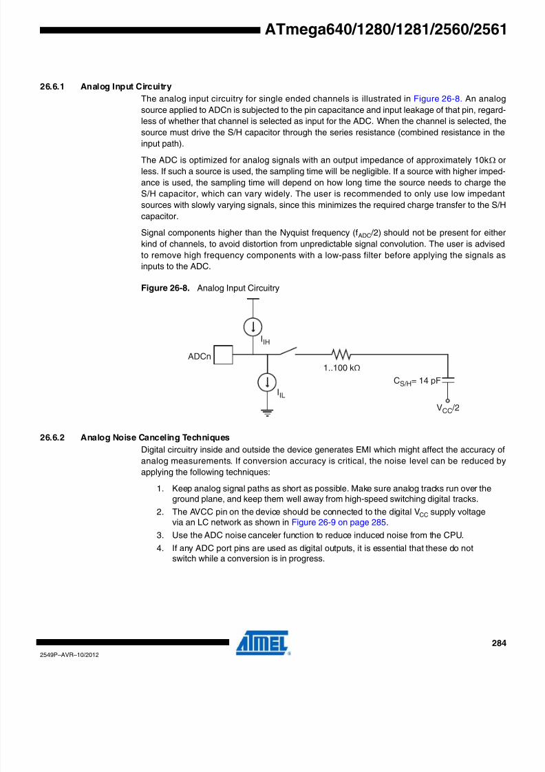
8/20/2019 At Mega 1281 Unlocked
http://slidepdf.com/reader/full/at-mega-1281-unlocked 284/446
284
2549P–AVR–10/2012
ATmega640/1280/1281/2560/2561
26.6.1 Analog Input Circuitry
The analog input circuitry for single ended channels is illustrated in Figure 26-8. An analog
source applied to ADCn is subjected to the pin capacitance and input leakage of that pin, regard
less of whether that channel is selected as input for the ADC. When the channel is selected, the
source must drive the S/H capacitor through the series resistance (combined resistance in theinput path).
The ADC is optimized for analog signals with an output impedance of approximately 10kΩ or
less. If such a source is used, the sampling time will be negligible. If a source with higher imped-
ance is used, the sampling time will depend on how long time the source needs to charge the
S/H capacitor, which can vary widely. The user is recommended to only use low impedant
sources with slowly varying signals, since this minimizes the required charge transfer to the S/H
capacitor.
Signal components higher than the Nyquist frequency (fADC /2) should not be present for eithe
kind of channels, to avoid distortion from unpredictable signal convolution. The user is advised
to remove high frequency components with a low-pass filter before applying the signals as
inputs to the ADC.
Figure 26-8. Analog Input Circuitry
26.6.2 Analog Noise Canceling Techniques
Digital circuitry inside and outside the device generates EMI which might affect the accuracy of
analog measurements. If conversion accuracy is critical, the noise level can be reduced by
applying the following techniques:
1. Keep analog signal paths as short as possible. Make sure analog tracks run over theground plane, and keep them well away from high-speed switching digital tracks.
2. The AVCC pin on the device should be connected to the digital VCC supply voltagevia an LC network as shown in Figure 26-9 on page 285.
3. Use the ADC noise canceler function to reduce induced noise from the CPU.
4. If any ADC port pins are used as digital outputs, it is essential that these do notswitch while a conversion is in progress.
ADCn
IIH
1..100 kΩ
CS/H= 14 pF
VCC /2IIL

8/20/2019 At Mega 1281 Unlocked
http://slidepdf.com/reader/full/at-mega-1281-unlocked 285/446
285
2549P–AVR–10/2012
ATmega640/1280/1281/2560/2561
Figure 26-9. ADC Power Connections, ATmega1281/2561.
Figure 26-10. ADC Power Connections, ATmega640/1280/2560
VCC
GND
100nF100nF
Ground Plane
(ADC0) PF0
(ADC7) PF7
(ADC1) PF1
(ADC2) PF2
(ADC3) PF3
(ADC4) PF4
(ADC5) PF5
(ADC6) PF6
AREF
GND
AVCC
52
53
54
55
56
57
58
59
60
6161
6262
6363
6464
1
51
P G 5
PA0
10µΗ
100nF
Ground Plane
100
(OC0B)PG5
10µΗ
79
80
81
82
83
84
85
86
87
88
89
90
91
92
93
94
95
96
97
98
99
PJ7
VCC
GND
(ADC15/PCINT23) PK7
(ADC14/PCINT22) PK6
(ADC13 /PCINT21) PK5
(ADC12/PCINT20) PK4
(ADC11/PCINT19) PK3
(ADC10/PCINT18) PK2
(ADC9/PCINT17) PK1
(ADC8/PCINT16) PK0
(ADC7/TDI) PF7
(ADC6/TDO) PF6
(ADC5/TMS) PF5
(ADC4/TCK) PF4
(ADC3) PF3
(ADC2) PF2
(ADC1) PF1
(ADC0) PF0
AREF
GND
AVCC
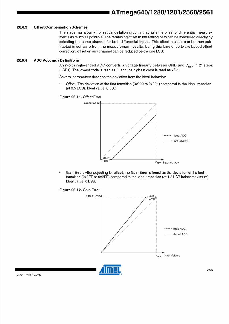
8/20/2019 At Mega 1281 Unlocked
http://slidepdf.com/reader/full/at-mega-1281-unlocked 286/446
286
2549P–AVR–10/2012
ATmega640/1280/1281/2560/2561
26.6.3 Offset Compensation Schemes
The stage has a built-in offset cancellation circuitry that nulls the offset of differential measure-
ments as much as possible. The remaining offset in the analog path can be measured directly by
selecting the same channel for both differential inputs. This offset residue can be then sub
tracted in software from the measurement results. Using this kind of software based offse
correction, offset on any channel can be reduced below one LSB.
26.6.4 ADC Accuracy Definitions
An n-bit single-ended ADC converts a voltage linearly between GND and VREF in 2n steps
(LSBs). The lowest code is read as 0, and the highest code is read as 2n-1.
Several parameters describe the deviation from the ideal behavior:
• Offset: The deviation of the first transition (0x000 to 0x001) compared to the ideal transition(at 0.5 LSB). Ideal value: 0 LSB.
Figure 26-11. Offset Error
• Gain Error: After adjusting for offset, the Gain Error is found as the deviation of the lasttransition (0x3FE to 0x3FF) compared to the ideal transition (at 1.5 LSB below maximum).Ideal value: 0 LSB.
Figure 26-12. Gain Error
Output Code
VREF Input Voltage
Ideal ADC
Actual ADC
OffsetError
Output Code
VREF Input Voltage
Ideal ADC
Actual ADC
GainError

8/20/2019 At Mega 1281 Unlocked
http://slidepdf.com/reader/full/at-mega-1281-unlocked 287/446
287
2549P–AVR–10/2012
ATmega640/1280/1281/2560/2561
• Integral Non-linearity (INL): After adjusting for offset and gain error, the INL is the maximumdeviation of an actual transition compared to an ideal transition for any code. Ideal value: 0LSB.
Figure 26-13. Integral Non-linearity (INL)
• Differential Non-linearity (DNL): The maximum deviation of the actual code width (theinterval between two adjacent transitions) from the ideal code width (1 LSB). Ideal value: 0LSB.
Figure 26-14. Differential Non-linearity (DNL)
• Quantization Error: Due to the quantization of the input voltage into a finite number of codes,a range of input voltages (1 LSB wide) will code to the same value. Always ±0.5 LSB.
• Absolute Accuracy: The maximum deviation of an actual (unadjusted) transition comparedto an ideal transition for any code. This is the compound effect of offset, gain error,differential error, non-linearity, and quantization error. Ideal value: ±0.5 LSB.
Output Code
VREF Input Voltage
Ideal ADC
Actual ADC
I N L
Output Code
0x3FF
0x000
0 VREF Input Voltage
DNL
1 LSB

8/20/2019 At Mega 1281 Unlocked
http://slidepdf.com/reader/full/at-mega-1281-unlocked 288/446
288
2549P–AVR–10/2012
ATmega640/1280/1281/2560/2561
26.7 ADC Conversion Result
After the conversion is complete (ADIF is high), the conversion result can be found in the ADC
Result Registers (ADCL, ADCH).
For single ended conversion, the result is
where VIN is the voltage on the selected input pin and VREF the selected voltage reference (see
Table 26-3 on page 289 and Table 26-4 on page 290). 0x000 represents analog ground, and
0x3FF represents the selected reference voltage minus one LSB.
If differential channels are used, the result is
where VPOS is the voltage on the positive input pin, VNEG the voltage on the negative input pin
and VREF the selected voltage reference. The result is presented in two’s complement form, from
0x200 (-512d) through 0x1FF (+511d). Note that if the user wants to perform a quick polarity
check of the result, it is sufficient to read the MSB of the result (ADC9 in ADCH). If the bit is one
the result is negative, and if this bit is zero, the result is positive. Figure 26-15 shows the decod
ing of the differential input range.
Table 26-2 on page 289 shows the resulting output codes if the differential input channel pai
(ADCn - ADCm) is selected with a gain of GAIN and a reference voltage of VREF.
Figure 26-15. Differential Measurement Range
AD C V IN 1024⋅
V RE F
--------------------------=
AD C V PO S V NE G–( ) 512⋅
V RE F
-----------------------------------------------------=
0
Output Code
0x1FF
0x000
VREF
Differential InputVoltage (Volts)
0x3FF
0x200
- VREF

8/20/2019 At Mega 1281 Unlocked
http://slidepdf.com/reader/full/at-mega-1281-unlocked 289/446
289
2549P–AVR–10/2012
ATmega640/1280/1281/2560/2561
Example:
ADMUX = 0xFB (ADC3 - ADC2, 10× gain, 2.56V reference, left adjusted result).Voltage on ADC3 is 300mV, voltage on ADC2 is 500mV.
ADCR = 512 × 10 × (300 - 500) / 2560 = -400 = 0x270.
ADCL will thus read 0x00, and ADCH will read 0x9C. Writing zero to ADLAR right adjusts the
result: ADCL = 0x70, ADCH = 0x02.
26.8 Register Description
26.8.1 ADMUX – ADC Multiplexer Selection Register
• Bit 7:6 – REFS1:0: Reference Selection Bits
These bits select the voltage reference for the ADC, as shown in Table 26-3. If these bits are
changed during a conversion, the change will not go in effect until this conversion is complete
(ADIF in ADCSRA is set). The internal voltage reference options may not be used if an externa
reference voltage is being applied to the AREF pin.
Note: 1. If 10x or 200x gain is selected, only 2.56V should be used as Internal Voltage Reference. Fordifferential conversion, only 1.1V cannot be used as internal voltage reference.
Table 26-2. Correlation Between Input Voltage and Output Codes
VADCn Read Code Corresponding Decimal Value
VADCm + VREF / GAIN 0x1FF 511
VADCm + 0.999 VREF / GAIN 0x1FF 511
VADCm + 0.998 VREF / GAIN 0x1FE 510
... ... ...
VADCm + 0.001 VREF / GAIN 0x001 1
VADCm 0x000 0
VADCm - 0.001 VREF / GAIN 0x3FF -1
... ... ...
VADCm - 0.999 VREF / GAIN 0x201 -511
VADCm - VREF / GAIN 0x200 -512
Bit 7 6 5 4 3 2 1 0
(0x7C) REFS1 REFS0 ADLAR MUX4 MUX3 MUX2 MUX1 MUX0 ADMUX
Read/ Write R/ W R/ W R/ W R/ W R/ W R/ W R/ W R/ W
Initial Value 0 0 0 0 0 0 0 0
Table 26-3. Voltage Reference Selections for ADC
REFS1 REFS0 Voltage Reference Selection(1)
0 0 AREF, Internal VREF turned off
0 1 AVCC with external capacitor at AREF pin
1 0 Internal 1.1V Voltage Reference with external capacitor at AREF pin
1 1 Internal 2.56V Voltage Reference with external capacitor at AREF pin
8/20/2019 At Mega 1281 Unlocked
http://slidepdf.com/reader/full/at-mega-1281-unlocked 290/446
290
2549P–AVR–10/2012
ATmega640/1280/1281/2560/2561
• Bit 5 – ADLAR: ADC Left Adjust Result
The ADLAR bit affects the presentation of the ADC conversion result in the ADC Data Register
Write one to ADLAR to left adjust the result. Otherwise, the result is right adjusted. Changing the
ADLAR bit will affect the ADC Data Register immediately, regardless of any ongoing conver-
sions. For a complete description of this bit, see “ADCL and ADCH – The ADC Data Register” on
page 294.
• Bits 4:0 – MUX4:0: Analog Channel and Gain Selection Bits
The value of these bits selects which combination of analog inputs are connected to the ADC.
See Table 26-4 for details. If these bits are changed during a conversion, the change will not go
in effect until this conversion is complete (ADIF in ADCSRA is set).
26.8.2 ADCSRB – ADC Control and Status Register B
• Bit 3 – MUX5: Analog Channel and Gain Selection BitThis bit is used together with MUX4:0 in ADMUX to select which combination in of analog inputs
are connected to the ADC. See Table 26-4 for details. If this bit is changed during a conversion
the change will not go in effect until this conversion is complete.
This bit is not valid for ATmega1281/2561.
Bit 7 6 5 4 3 2 1 0
(0x7B) – ACME – – MUX5 ADTS2 ADTS1 ADTS0 ADCSRB
Read/ Write R R/ W R R R/ W R/ W R/ W R/ W
Initial Value 0 0 0 0 0 0 0 0
Table 26-4. Input Channel Selections
MUX5:0
Single Ended
Input
Positive Differential
Input
Negative Differential
Input Gain
000000 ADC0
N /A
000001 ADC1
000010 ADC2
000011 ADC3
000100 ADC4
000101 ADC5
000110 ADC6
000111 ADC7

8/20/2019 At Mega 1281 Unlocked
http://slidepdf.com/reader/full/at-mega-1281-unlocked 291/446
291
2549P–AVR–10/2012
ATmega640/1280/1281/2560/2561
001000(1)
N /A
ADC0 ADC0 10×
001001(1) ADC1 ADC0 10×
001010(1) ADC0 ADC0 200×
001011(1) ADC1 ADC0 200×
001100(1) ADC2 ADC2 10×
001101(1) ADC3 ADC2 10×
001110(1) ADC2 ADC2 200×
001111(1) ADC3 ADC2 200×
010000 ADC0 ADC1 1×
010001 ADC1 ADC1 1×
010010 ADC2 ADC1 1×
010011 ADC3 ADC1 1×
010100 ADC4 ADC1 1×
010101 ADC5 ADC1 1×
010110 ADC6 ADC1 1×
010111 ADC7 ADC1 1×
011000 ADC0 ADC2 1×
011001 ADC1 ADC2 1×
011010
N /A
ADC2 ADC2 1×
011011 ADC3 ADC2 1×
011100 ADC4 ADC2 1×
011101 ADC5 ADC2 1×
011110 1.1V (VBG)N /A
011111 0V (GND)
100000 ADC8
N /A
100001 ADC9
100010 ADC10
100011 ADC11
100100 ADC12
100101 ADC13
100110 ADC14
100111 ADC15
Table 26-4. Input Channel Selections (Continued)
MUX5:0
Single Ended
Input
Positive Differential
Input
Negative Differential
Input Gain
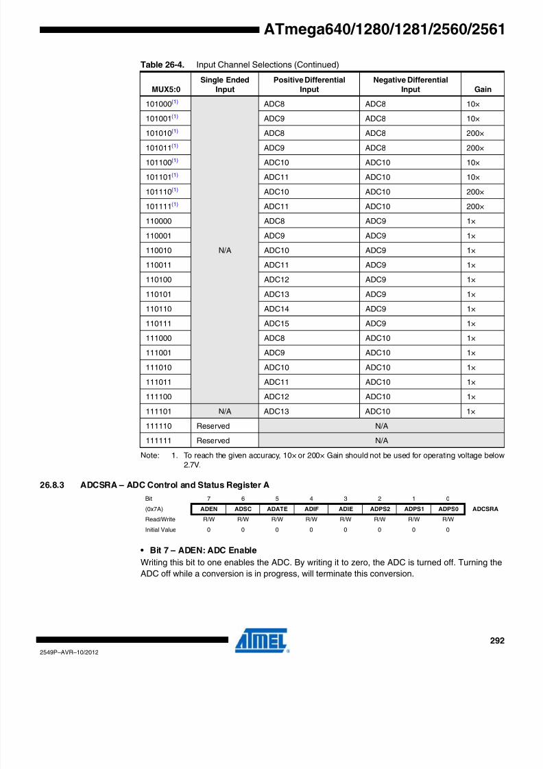
8/20/2019 At Mega 1281 Unlocked
http://slidepdf.com/reader/full/at-mega-1281-unlocked 292/446
292
2549P–AVR–10/2012
ATmega640/1280/1281/2560/2561
Note: 1. To reach the given accuracy, 10× or 200× Gain should not be used for operating voltage below2.7V.
26.8.3 ADCSRA – ADC Control and Status Register A
• Bit 7 – ADEN: ADC Enable
Writing this bit to one enables the ADC. By writing it to zero, the ADC is turned off. Turning the
ADC off while a conversion is in progress, will terminate this conversion.
101000(1)
N /A
ADC8 ADC8 10×
101001(1) ADC9 ADC8 10×
101010(1) ADC8 ADC8 200×
101011(1) ADC9 ADC8 200×
101100(1) ADC10 ADC10 10×
101101(1) ADC11 ADC10 10×
101110(1) ADC10 ADC10 200×
101111(1) ADC11 ADC10 200×
110000 ADC8 ADC9 1×
110001 ADC9 ADC9 1×
110010 ADC10 ADC9 1×
110011 ADC11 ADC9 1×
110100 ADC12 ADC9 1×
110101 ADC13 ADC9 1×
110110 ADC14 ADC9 1×
110111 ADC15 ADC9 1×
111000 ADC8 ADC10 1×
111001 ADC9 ADC10 1×
111010 ADC10 ADC10 1×
111011 ADC11 ADC10 1×
111100 ADC12 ADC10 1×
111101 N /A ADC13 ADC10 1×
111110 Reserved N /A
111111 Reserved N /A
Table 26-4. Input Channel Selections (Continued)
MUX5:0
Single Ended
Input
Positive Differential
Input
Negative Differential
Input Gain
Bit 7 6 5 4 3 2 1 0
(0x7A) ADEN ADSC ADATE ADIF ADIE ADPS2 ADPS1 ADPS0 ADCSRA
Read/ Write R/ W R/ W R/ W R/ W R/ W R/ W R/ W R/ W
Initial Value 0 0 0 0 0 0 0 0
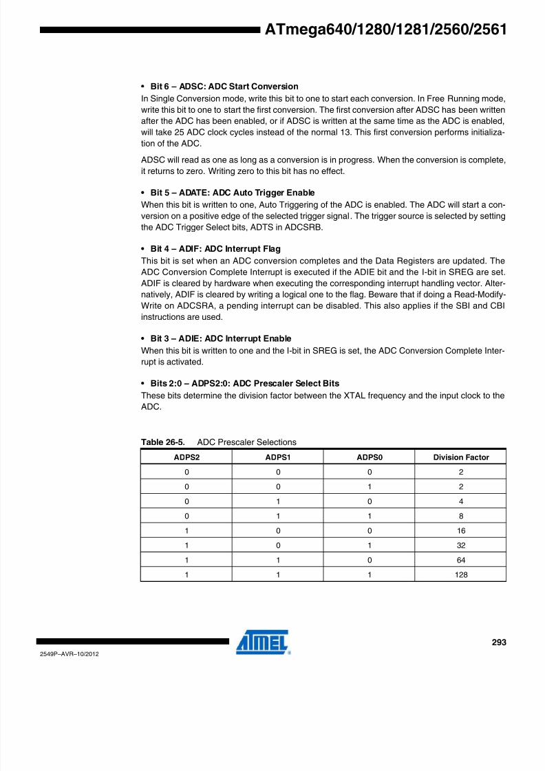
8/20/2019 At Mega 1281 Unlocked
http://slidepdf.com/reader/full/at-mega-1281-unlocked 293/446
293
2549P–AVR–10/2012
ATmega640/1280/1281/2560/2561
• Bit 6 – ADSC: ADC Start Conversion
In Single Conversion mode, write this bit to one to start each conversion. In Free Running mode
write this bit to one to start the first conversion. The first conversion after ADSC has been written
after the ADC has been enabled, or if ADSC is written at the same time as the ADC is enabled,
will take 25 ADC clock cycles instead of the normal 13. This first conversion performs initializa-tion of the ADC.
ADSC will read as one as long as a conversion is in progress. When the conversion is complete
it returns to zero. Writing zero to this bit has no effect.
• Bit 5 – ADATE: ADC Auto Trigger Enable
When this bit is written to one, Auto Triggering of the ADC is enabled. The ADC will start a con-
version on a positive edge of the selected trigger signal. The trigger source is selected by setting
the ADC Trigger Select bits, ADTS in ADCSRB.
• Bit 4 – ADIF: ADC Interrupt Flag
This bit is set when an ADC conversion completes and the Data Registers are updated. TheADC Conversion Complete Interrupt is executed if the ADIE bit and the I-bit in SREG are set
ADIF is cleared by hardware when executing the corresponding interrupt handling vector. Alter-
natively, ADIF is cleared by writing a logical one to the flag. Beware that if doing a Read-Modify
Write on ADCSRA, a pending interrupt can be disabled. This also applies if the SBI and CBI
instructions are used.
• Bit 3 – ADIE: ADC Interrupt Enable
When this bit is written to one and the I-bit in SREG is set, the ADC Conversion Complete Inter-
rupt is activated.
• Bits 2:0 – ADPS2:0: ADC Prescaler Select Bits
These bits determine the division factor between the XTAL frequency and the input clock to theADC.
Table 26-5. ADC Prescaler Selections
ADPS2 ADPS1 ADPS0 Division Factor
0 0 0 2
0 0 1 2
0 1 0 4
0 1 1 8
1 0 0 16
1 0 1 32
1 1 0 64
1 1 1 128

8/20/2019 At Mega 1281 Unlocked
http://slidepdf.com/reader/full/at-mega-1281-unlocked 294/446
294
2549P–AVR–10/2012
ATmega640/1280/1281/2560/2561
26.8.4 ADCL and ADCH – The ADC Data Register
26.8.4.1 ADLAR = 0
26.8.4.2 ADLAR = 1
When an ADC conversion is complete, the result is found in these two registers. If differentia
channels are used, the result is presented in two’s complement form.
When ADCL is read, the ADC Data Register is not updated until ADCH is read. Consequently, i
the result is left adjusted and no more than 8-bit precision (7 bit + sign bit for differential inpu
channels) is required, it is sufficient to read ADCH. Otherwise, ADCL must be read first, then
ADCH.
The ADLAR bit in ADMUX, and the MUXn bits in ADMUX affect the way the result is read from
the registers. If ADLAR is set, the result is left adjusted. If ADLAR is cleared (default), the resul
is right adjusted.
• ADC9:0: ADC Conversion Result
These bits represent the result from the conversion, as detailed in “ADC Conversion Result” on
page 288.
26.8.5 ADCSRB – ADC Control and Status Register B
• Bit 7 – Res: Reserved Bit
This bit is reserved for future use. To ensure compatibility with future devices, this bit must be
written to zero when ADCSRB is written.
• Bit 2:0 – ADTS2:0: ADC Auto Trigger Source
If ADATE in ADCSRA is written to one, the value of these bits selects which source will trigger
an ADC conversion. If ADATE is cleared, the ADTS2:0 settings will have no effect. A conversion
will be triggered by the rising edge of the selected Interrupt Flag. Note that switching from a trig-
Bit 15 14 13 12 11 10 9 8
(0x79) – – – – – – ADC9 ADC8 ADCH
(0x78) ADC7 ADC6 ADC5 ADC4 ADC3 ADC2 ADC1 ADC0 ADCL
7 6 5 4 3 2 1 0Read/ Write R R R R R R R R
R R R R R R R R
Initial Value 0 0 0 0 0 0 0 0
0 0 0 0 0 0 0 0
Bit 15 14 13 12 11 10 9 8
(0x79) ADC9 ADC8 ADC7 ADC6 ADC5 ADC4 ADC3 ADC2 ADCH
(0x78) ADC1 ADC0 – – – – – – ADCL
7 6 5 4 3 2 1 0
Read/ Write R R R R R R R R
R R R R R R R RInitial Value 0 0 0 0 0 0 0 0
0 0 0 0 0 0 0 0
Bit 7 6 5 4 3 2 1 0
(0x7B) – ACME – – MUX5 ADTS2 ADTS1 ADTS0 ADCSRB
Read/ Write R R/ W R R R/ W R/ W R/ W R/ W
Initial Value 0 0 0 0 0 0 0 0

8/20/2019 At Mega 1281 Unlocked
http://slidepdf.com/reader/full/at-mega-1281-unlocked 295/446
295
2549P–AVR–10/2012
ATmega640/1280/1281/2560/2561
ger source that is cleared to a trigger source that is set, will generate a positive edge on the
trigger signal. If ADEN in ADCSRA is set, this will start a conversion. Switching to Free Running
mode (ADTS[2:0]=0) will not cause a trigger event, even if the ADC Interrupt Flag is set.
Note: Free running mode cannot be used for differential channels (see chapter “Differential Channels”
on page 281).
26.8.6 DIDR0 – Digital Input Disable Register 0
• Bit 7:0 – ADC7D:ADC0D: ADC7:0 Digital Input Disable
When this bit is written logic one, the digital input buffer on the corresponding ADC pin is dis
abled. The corresponding PIN Register bit will always read as zero when this bit is set. When an
analog signal is applied to the ADC7:0 pin and the digital input from this pin is not needed, this
bit should be written logic one to reduce power consumption in the digital input buffer.
26.8.7 DIDR2 – Digital Input Disable Register 2
• Bit 7:0 – ADC15D:ADC8D: ADC15:8 Digital Input Disable
When this bit is written logic one, the digital input buffer on the corresponding ADC pin is dis
abled. The corresponding PIN Register bit will always read as zero when this bit is set. When an
analog signal is applied to the ADC15:8 pin and the digital input from this pin is not needed, this
bit should be written logic one to reduce power consumption in the digital input buffer.
Table 26-6. ADC Auto Trigger Source Selections
ADTS2 ADTS1 ADTS0 Trigger Source
0 0 0 Free Running mode
0 0 1 Analog Comparator
0 1 0 External Interrupt Request 0
0 1 1 Timer/Counter0 Compare Match A
1 0 0 Timer/Counter0 Overflow
1 0 1 Timer/Counter1 Compare Match B
1 1 0 Timer/Counter1 Overflow
1 1 1 Timer/Counter1 Capture Event
Bit 7 6 5 4 3 2 1 0
(0x7E) ADC7D ADC6D ADC5D ADC4D ADC3D ADC2D ADC1D ADC0D DIDR0
Read/ Write R/ W R/ W R/ W R/ W R/ W R/ W R/ W R/ W
Initial Value 0 0 0 0 0 0 0 0
Bit 7 6 5 4 3 2 1 0
(0x7D) ADC15D ADC14D ADC13D ADC12D ADC11D ADC10D ADC9D ADC8D DIDR2
Read/ Write R/ W R/ W R/ W R/ W R/ W R/ W R/ W R/ W
Initial Value 0 0 0 0 0 0 0 0
8/20/2019 At Mega 1281 Unlocked
http://slidepdf.com/reader/full/at-mega-1281-unlocked 296/446
296
2549P–AVR–10/2012
ATmega640/1280/1281/2560/2561
27. JTAG Interface and On-chip Debug System
27.1 Features• JTAG (IEEE std. 1149.1 Compliant) Interface
• Boundary-scan Capabilities According to the IEEE std. 1149.1 (JTAG) Standard
• Debugger Access to:
– All Internal Peripheral Units
– Internal and External RAM
– The Internal Register File
– Program Counter
– EEPROM and Flash Memories
• Extensive On-chip Debug Support for Break Conditions, Including
– AVR Break Instruction
– Break on Change of Program Memory Flow
– Single Step Break
– Program Memory Break Points on Single Address or Address Range
– Data Memory Break Points on Single Address or Address Range
• Programming of Flash, EEPROM, Fuses, and Lock Bits through the JTAG Interface• On-chip Debugging Supported by AVR Studio ®
27.2 Overview
The AVR IEEE std. 1149.1 compliant JTAG interface can be used for
• Testing PCBs by using the JTAG Boundary-scan capability
• Programming the non-volatile memories, Fuses and Lock bits
• On-chip debugging
A brief description is given in the following sections. Detailed descriptions for Programming via
the JTAG interface, and using the Boundary-scan Chain can be found in the sections “Program
ming via the JTAG Interface” on page 354 and “IEEE 1149.1 (JTAG) Boundary-scan” on page
302, respectively. The On-chip Debug support is considered being private JTAG instructionsand distributed within Atmel and to selected third party vendors only.
Figure 27-1 on page 297 shows a block diagram of the JTAG interface and the On-chip Debug
system. The TAP Controller is a state machine controlled by the TCK and TMS signals. The TAP
Controller selects either the JTAG Instruction Register or one of several Data Registers as the
scan chain (Shift Register) between the TDI – input and TDO – output. The Instruction Register
holds JTAG instructions controlling the behavior of a Data Register.
The ID-Register, Bypass Register, and the Boundary-scan Chain are the Data Registers used
for board-level testing. The JTAG Programming Interface (actually consisting of several physica
and virtual Data Registers) is used for serial programming via the JTAG interface. The Interna
Scan Chain and Break Point Scan Chain are used for On-chip debugging only.

8/20/2019 At Mega 1281 Unlocked
http://slidepdf.com/reader/full/at-mega-1281-unlocked 297/446
297
2549P–AVR–10/2012
ATmega640/1280/1281/2560/2561
Figure 27-1. Block Diagram
27.3 TAP - Test Access Port
The JTAG interface is accessed through four of the AVR’s pins. In JTAG terminology, these pinsconstitute the Test Access Port – TAP. These pins are:
• TMS: Test mode select. This pin is used for navigating through the TAP-controller statemachine.
• TCK: Test Clock. JTAG operation is synchronous to TCK.
• TDI: Test Data In. Serial input data to be shifted in to the Instruction Register or DataRegister (Scan Chains).
• TDO: Test Data Out. Serial output data from Instruction Register or Data Register.
The IEEE std. 1149.1 also specifies an optional TAP signal; TRST – Test ReSeT – which is not
provided.
When the JTAGE
N Fuse is unprogrammed, these four TAP pins are normal port pins, and theTAP controller is in reset. When programmed, the input TAP signals are internally pulled high
and the JTAG is enabled for Boundary-scan and programming. The device is shipped with this
fuse programmed.
For the On-chip Debug system, in addition to the JTAG interface pins, the RESET pin is moni-
tored by the debugger to be able to detect external reset sources. The debugger can also pul
the RESET pin low to reset the whole system, assuming only open collectors on the reset line
are used in the application.
TAPCONTROLLER
TDI
TDO
TCK
TMS
FLASHMEMORY
AVR CPU
DIGITALPERIPHERAL
UNITS
JTAG / AVR CORE
COMMUNICATIONINTERFACE
BREAKPOINTUNIT
FLOW CONTROLUNIT
OCD STATUS
AND CONTROL
INTERNALSCANCHAIN
MUX
INSTRUCTIONREGISTER
IDREGISTER
BYPASSREGISTER
JTAG PROGRAMMINGINTERFACE
PCInstruction
AddressData
BREAKPOINTSCAN CHAIN
ADDRESSDECODER
ANALOGPERIPHERIAL
UNITS
I/O PORT 0
I/O PORT n
BOUNDARY SCAN CHAIN
Analog inputs
Control & Clock lines
DEVICE BOUNDARY
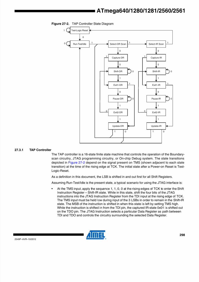
8/20/2019 At Mega 1281 Unlocked
http://slidepdf.com/reader/full/at-mega-1281-unlocked 298/446
298
2549P–AVR–10/2012
ATmega640/1280/1281/2560/2561
Figure 27-2. TAP Controller State Diagram
27.3.1 TAP Controller
The TAP controller is a 16-state finite state machine that controls the operation of the Boundary
scan circuitry, JTAG programming circuitry, or On-chip Debug system. The state transitions
depicted in Figure 27-2 depend on the signal present on TMS (shown adjacent to each state
transition) at the time of the rising edge at TCK. The initial state after a Power-on Reset is Test
Logic-Reset.
As a definition in this document, the LSB is shifted in and out first for all Shift Registers.
Assuming Run-Test/Idle is the present state, a typical scenario for using the JTAG interface is:
• At the TMS input, apply the sequence 1, 1, 0, 0 at the rising edges of TCK to enter the Shift
Instruction Register – Shift-IR state. While in this state, shift the four bits of the JTAGinstructions into the JTAG Instruction Register from the TDI input at the rising edge of TCK.The TMS input must be held low during input of the 3 LSBs in order to remain in the Shift-IRstate. The MSB of the instruction is shifted in when this state is left by setting TMS high.While the instruction is shifted in from the TDI pin, the captured IR-state 0x01 is shifted outon the TDO pin. The JTAG Instruction selects a particular Data Register as path betweenTDI and TDO and controls the circuitry surrounding the selected Data Register.
Test-Logic-Reset
Run-Test/Idle
Shift-DR
Exit1-DR
Pause-DR
Exit2-DR
Update-DR
Select-IR Scan
Capture-IR
Shift-IR
Exit1-IR
Pause-IR
Exit2-IR
Update-IR
Select-DR Scan
Capture-DR
0
1
0 1 1 1
0 0
0 0
1 1
1 0
1
1
0
1
0
0
1 0
1
1
0
1
0
0
00
11

8/20/2019 At Mega 1281 Unlocked
http://slidepdf.com/reader/full/at-mega-1281-unlocked 299/446
299
2549P–AVR–10/2012
ATmega640/1280/1281/2560/2561
• Apply the TMS sequence 1, 1, 0 to re-enter the Run-Test/Idle state. The instruction islatched onto the parallel output from the Shift Register path in the Update-IR state. The ExitIR, Pause-IR, and Exit2-IR states are only used for navigating the state machine.
• At the TMS input, apply the sequence 1, 0, 0 at the rising edges of TCK to enter the ShiftData Register – Shift-DR state. While in this state, upload the selected Data Register(selected by the present JTAG instruction in the JTAG Instruction Register) from the TDI
input at the rising edge of TCK. In order to remain in the Shift-DR state, the TMS input mustbe held low during input of all bits except the MSB. The MSB of the data is shifted in whenthis state is left by setting TMS high. While the Data Register is shifted in from the TDI pin,the parallel inputs to the Data Register captured in the Capture-DR state is shifted out on theTDO pin.
• Apply the TMS sequence 1, 1, 0 to re-enter the Run-Test/Idle state. If the selected DataRegister has a latched parallel-output, the latching takes place in the Update-DR state. TheExit-DR, Pause-DR, and Exit2-DR states are only used for navigating the state machine.
As shown in the state diagram, the Run-Test/Idle state need not be entered between selecting
JTAG instruction and using Data Registers, and some JTAG instructions may select certain
functions to be performed in the Run-Test/Idle, making it unsuitable as an Idle state.
Note: Independent of the initial state of the TAP Controller, the Test-Logic-Reset state can always be
entered by holding TMS high for five TCK clock periods.
For detailed information on the JTAG specification, refer to the literature listed in “Bibliography”
on page 301.
27.4 Using the Boundary-scan Chain
A complete description of the Boundary-scan capabilities are given in the section “IEEE 1149.1
(JTAG) Boundary-scan” on page 302.
27.5 Using the On-chip Debug System
As shown in Figure 27-1 on page 297, the hardware support for On-chip Debugging consists
mainly of:
• A scan chain on the interface between the internal AVR CPU and the internal peripheralunits
• Break Point unit
• Communication interface between the CPU and JTAG system
All read or modify/write operations needed for implementing the Debugger are done by applying
AVR instructions via the internal AVR CPU Scan Chain. The CPU sends the result to an I/O
memory mapped location which is part of the communication interface between the CPU and the
JTAG system.
The Break Point Unit implements Break on Change of Program Flow, Single Step Break, two
Program Memory Break Points, and two combined Break Points. Together, the four Break
Points can be configured as either:• 4 single Program Memory Break Points
• 3 Single Program Memory Break Point + 1 single Data Memory Break Point
• 2 single Program Memory Break Points + 2 single Data Memory Break Points
• 2 single Program Memory Break Points + 1 Program Memory Break Point with mask (“rangeBreak Point”)
• 2 single Program Memory Break Points + 1 Data Memory Break Point with mask (“rangeBreak Point”)

8/20/2019 At Mega 1281 Unlocked
http://slidepdf.com/reader/full/at-mega-1281-unlocked 300/446
300
2549P–AVR–10/2012
ATmega640/1280/1281/2560/2561
A debugger, like the AVR Studio, may however use one or more of these resources for its inter-
nal purpose, leaving less flexibility to the end-user.
A list of the On-chip Debug specific JTAG instructions is given in “On-chip Debug Specific JTAG
Instructions” on page 300.
The JTAGEN Fuse must be programmed to enable the JTAG Test Access Port. In addition, the
OCDEN Fuse must be programmed and no Lock bits must be set for the On-chip debug systemto work. As a security feature, the On-chip debug system is disabled when either of the LB1 o
LB2 Lock bits are set. Otherwise, the On-chip debug system would have provided a back-door
into a secured device.
The AVR Studio ® enables the user to fully control execution of programs on an AVR device with
On-chip Debug capability, AVR In-Circuit Emulator, or the built-in AVR Instruction Set Simulator
AVR Studio supports source level execution of Assembly programs assembled with Atmel Cor-
poration’s AVR Assembler and C programs compiled with third party vendors’ compilers.
AVR Studio runs under Microsoft ® Windows ® 95/98/2000 and Microsoft Windows NT ® .
For a full description of the AVR Studio, please refer to the AVR Studio User Guide. Only high-
lights are presented in this document.All necessary execution commands are available in AVR Studio, both on source level and on
disassembly level. The user can execute the program, single step through the code either by
tracing into or stepping over functions, step out of functions, place the cursor on a statement and
execute until the statement is reached, stop the execution, and reset the execution target. In
addition, the user can have an unlimited number of code Break Points (using the BREAK
instruction) and up to two data memory Break Points, alternatively combined as a mask (range
Break Point.
27.6 On-chip Debug Specific JTAG Instructions
The On-chip debug support is considered being private JTAG instructions, and distributed within
ATMEL and to selected third party vendors only. Instruction opcodes are listed for reference.
27.6.1 PRIVATE0; 0x8
Private JTAG instruction for accessing On-chip debug system.
27.6.2 PRIVATE1; 0x9
Private JTAG instruction for accessing On-chip debug system.
27.6.3 PRIVATE2; 0xA
Private JTAG instruction for accessing On-chip debug system.
27.6.4 PRIVATE3; 0xB
Private JTAG instruction for accessing On-chip debug system.

8/20/2019 At Mega 1281 Unlocked
http://slidepdf.com/reader/full/at-mega-1281-unlocked 301/446
301
2549P–AVR–10/2012
ATmega640/1280/1281/2560/2561
27.7 Using the JTAG Programming Capabilities
Programming of AVR parts via JTAG is performed via the 4-pin JTAG port, TCK, TMS, TDI, and
TDO. These are the only pins that need to be controlled/observed to perform JTAG program
ming (in addition to power pins). It is not required to apply 12V externally. The JTAGEN Fuse
must be programmed and the JTD bit in the MCUCR Register must be cleared to enable the
JTAG Test Access Port.
The JTAG programming capability supports:
• Flash programming and verifying
• EEPROM programming and verifying
• Fuse programming and verifying
• Lock bit programming and verifying
The Lock bit security is exactly as in parallel programming mode. If the Lock bits LB1 or LB2 are
programmed, the OCDEN Fuse cannot be programmed unless first doing a chip erase. This is a
security feature that ensures no back-door exists for reading out the content of a secured
device.
The details on programming through the JTAG interface and programming specific JTAG
instructions are given in the section “Programming via the JTAG Interface” on page 354.
27.8 Bibliography
For more information about general Boundary-scan, the following literature can be consulted:
• IEEE: IEEE Std. 1149.1-1990. IEEE Standard Test Access Port and Boundary-scanArchitecture, IEEE, 1993
• Colin Maunder: The Board Designers Guide to Testable Logic Circuits, Addison-Wesley,1992
27.9 On-chip Debug Related Register in I/O Memory
27.9.1 OCDR – On-chip Debug Register
The OCDR Register provides a communication channel from the running program in the micro-
controller to the debugger. The CPU can transfer a byte to the debugger by writing to this
location. At the same time, an internal flag; I/O Debug Register Dirty – IDRD – is set to indicate
to the debugger that the register has been written. When the CPU reads the OCDR Register the
7 LSB will be from the OCDR Register, while the MSB is the IDRD bit. The debugger clears theIDRD bit when it has read the information.
In some AVR devices, this register is shared with a standard I/O location. In this case, the OCDR
Register can only be accessed if the OCDEN Fuse is programmed, and the debugger enables
access to the OCDR Register. In all other cases, the standard I/O location is accessed.
Refer to the debugger documentation for further information on how to use this register.
Bit 7 6 5 4 3 2 1 0
0x31 (0x51) MSB/IDRD LSB OCDR
Read/ Write R/ W R/ W R/ W R/ W R/ W R/ W R/ W R/ W
Initial Value 0 0 0 0 0 0 0 0

8/20/2019 At Mega 1281 Unlocked
http://slidepdf.com/reader/full/at-mega-1281-unlocked 302/446
302
2549P–AVR–10/2012
ATmega640/1280/1281/2560/2561
28. IEEE 1149.1 (JTAG) Boundary-scan
28.1 Features• JTAG (IEEE std. 1149.1 compliant) Interface
• Boundary-scan Capabilities According to the JTAG Standard
• Full Scan of all Port Functions as well as Analog Circuitry having Off-chip Connections
• Supports the Optional IDCODE Instruction
• Additional Public AVR_RESET Instruction to Reset the AVR
28.2 System Overview
The Boundary-scan chain has the capability of driving and observing the logic levels on the digi
tal I/O pins, as well as the boundary between digital and analog logic for analog circuitry having
off-chip connections. At system level, all ICs having JTAG capabilities are connected serially by
the TDI/TDO signals to form a long Shift Register. An external controller sets up the devices to
drive values at their output pins, and observe the input values received from other devices. The
controller compares the received data with the expected result. In this way, Boundary-scan pro-
vides a mechanism for testing interconnections and integrity of components on Printed Circuits
Boards by using the four TAP signals only.
The four IEEE 1149.1 defined mandatory JTAG instructions IDCODE, BYPASS, SAMPLE/PRE-
LOAD, and EXTEST, as well as the AVR specific public JTAG instruction AVR_RESET can be
used for testing the Printed Circuit Board. Initial scanning of the Data Register path will show the
ID-Code of the device, since IDCODE is the default JTAG instruction. It may be desirable to
have the AVR device in reset during test mode. If not reset, inputs to the device may be deter
mined by the scan operations, and the internal software may be in an undetermined state when
exiting the test mode. Entering reset, the outputs of any port pin will instantly enter the high
impedance state, making the HIGHZ instruction redundant. If needed, the BYPASS instruction
can be issued to make the shortest possible scan chain through the device. The device can be
set in the reset state either by pulling the external RESET pin low, or issuing the AVR_RESET
instruction with appropriate setting of the Reset Data Register.The EXTEST instruction is used for sampling external pins and loading output pins with data
The data from the output latch will be driven out on the pins as soon as the EXTEST instruction
is loaded into the JTAG IR-Register. Therefore, the SAMPLE/PRELOAD should also be used fo
setting initial values to the scan ring, to avoid damaging the board when issuing the EXTEST
instruction for the first time. SAMPLE/PRELOAD can also be used for taking a snapshot of the
external pins during normal operation of the part.
The JTAGEN Fuse must be programmed and the JTD bit in the I/O Register MCUCR must be
cleared to enable the JTAG Test Access Port.
When using the JTAG interface for Boundary-scan, using a JTAG TCK clock frequency higher
than the internal chip frequency is possible. The chip clock is not required to run.
28.3 Data Registers
The Data Registers relevant for Boundary-scan operations are:
• Bypass Register
• Device Identification Register
• Reset Register
• Boundary-scan Chain

8/20/2019 At Mega 1281 Unlocked
http://slidepdf.com/reader/full/at-mega-1281-unlocked 303/446
303
2549P–AVR–10/2012
ATmega640/1280/1281/2560/2561
28.3.1 Bypass Register
The Bypass Register consists of a single Shift Register stage. When the Bypass Register is
selected as path between TDI and TDO, the register is reset to 0 when leaving the Capture-DR
controller state. The Bypass Register can be used to shorten the scan chain on a system when
the other devices are to be tested.
28.3.2 Device Identification RegisterFigure 28-1 shows the structure of the Device Identification Register.
Figure 28-1. The Format of the Device Identification Register
28.3.2.1 Version
Version is a 4-bit number identifying the revision of the component. The JTAG version number
follows the revision of the device. Revision A is 0x0, revision B is 0x1 and so on.
28.3.2.2 Part Number
The part number is a 16-bit code identifying the component. The JTAG Part Number fo
ATmega640/1280/1281/2560/2561 is l isted in Table 30-6 on page 338.
28.3.2.3 Manufacturer ID
The Manufacturer ID is a 11-bit code identifying the manufacturer. The JTAG manufacturer ID
for ATMEL is listed in Table 30-6 on page 338.
28.3.3 Reset Register
The Reset Register is a test Data Register used to reset the part. Since the AVR tri-states PortPins when reset, the Reset Register can also replace the function of the unimplemented optiona
JTAG instruction HIGHZ.
A high value in the Reset Register corresponds to pulling the external Reset low. The part is
reset as long as there is a high value present in the Reset Register. Depending on the fuse set
tings for the clock options, the part will remain reset for a reset time-out period (see “Clock
Sources” on page 41) after releasing the Reset Register. The output from this Data Register is
not latched, so the reset will take place immediately, as shown in Figure 28-2 on page 304.
MSB LSB
Bit 31 28 27 12 11 1 0
Device ID Version Part Number Manufacturer ID 1
4 bits 16 bits 11 bits 1-bit

8/20/2019 At Mega 1281 Unlocked
http://slidepdf.com/reader/full/at-mega-1281-unlocked 304/446
304
2549P–AVR–10/2012
ATmega640/1280/1281/2560/2561
Figure 28-2. Reset Register
28.3.4 Boundary-scan Chain
The Boundary-scan Chain has the capability of driving and observing the logic levels on the dig
ital I/O pins, as well as the boundary between digital and analog logic for analog circuitry havingoff-chip connections.
See “Boundary-scan Chain” on page 305 for a complete description.
28.4 Boundary-scan Specific JTAG Instructions
The Instruction Register is 4-bit wide, supporting up to 16 instructions. Listed below are the
JTAG instructions useful for Boundary-scan operation. Note that the optional HIGHZ instruction
is not implemented, but all outputs with tri-state capability can be set in high-impedant state by
using the AVR_RESET instruction, since the initial state for all port pins is tri-state.
As a definition in this datasheet, the LSB is shifted in and out first for all Shift Registers.
The OPCODE for each instruction is shown behind the instruction name in hex format. The textdescribes which Data Register is selected as path between TDI and TDO for each instruction.
28.4.1 EXTEST; 0x0
Mandatory JTAG instruction for selecting the Boundary-scan Chain as Data Register for testing
circuitry external to the AVR package. For port-pins, Pull-up Disable, Output Control, Output
Data, and Input Data are all accessible in the scan chain. For Analog circuits having off-chip
connections, the interface between the analog and the digital logic is in the scan chain. The con-
tents of the latched outputs of the Boundary-scan chain is driven out as soon as the JTAG IR
Register is loaded with the EXTEST instruction.
The active states are:
• Capture-DR: Data on the external pins are sampled into the Boundary-scan Chain
• Shift-DR: The Internal Scan Chain is shifted by the TCK input
• Update-DR: Data from the scan chain is applied to output pins
28.4.2 IDCODE; 0x1
Optional JTAG instruction selecting the 32-bit ID-Register as Data Register. The ID-Registe
consists of a version number, a device number and the manufacturer code chosen by JEDEC.
This is the default instruction after power-up.
D QFrom
TDI
ClockDR · AVR_RESET
To
TDO
From Other Internal and
External Reset Sources
Internal reset

8/20/2019 At Mega 1281 Unlocked
http://slidepdf.com/reader/full/at-mega-1281-unlocked 305/446
305
2549P–AVR–10/2012
ATmega640/1280/1281/2560/2561
The active states are:
• Capture-DR: Data in the IDCODE Register is sampled into the Boundary-scan Chain
• Shift-DR: The IDCODE scan chain is shifted by the TCK input
28.4.3 SAMPLE_PRELOAD; 0x2
Mandatory JTAG instruction for pre-loading the output latches and taking a snap-shot of theinput/output pins without affecting the system operation. However, the output latches are not
connected to the pins. The Boundary-scan Chain is selected as Data Register.
The active states are:
• Capture-DR: Data on the external pins are sampled into the Boundary-scan Chain
• Shift-DR: The Boundary-scan Chain is shifted by the TCK input
• Update-DR: Data from the Boundary-scan chain is applied to the output latches. However,the output latches are not connected to the pins
28.4.4 AVR_RESET; 0xC
The AVR specific public JTAG instruction for forcing the AVR device into the Reset mode o
releasing the JTAG reset source. The TAP controller is not reset by this instruction. The one bitReset Register is selected as Data Register. Note that the reset will be active as long as there is
a logic “one” in the Reset Chain. The output from this chain is not latched.
The active states are:
• Shift-DR: The Reset Register is shifted by the TCK input
28.4.5 BYPASS; 0xF
Mandatory JTAG instruction selecting the Bypass Register for Data Register.
The active states are:
• Capture-DR: Loads a logic “0” into the Bypass Register
• Shift-DR: The Bypass Register cell between TDI and TDO is shifted
28.5 Boundary-scan Chain
The Boundary-scan chain has the capability of driving and observing the logic levels on the digi
tal I/O pins, as well as the boundary between digital and analog logic for analog circuitry having
off-chip connection.
28.5.1 Scanning the Digital Port Pins
Figure 28-3 on page 306 shows the Boundary-scan Cell for a bi-directional port pin. The pull-up
function is disabled during Boundary-scan when the JTAG IC contains EXTEST or
SAMPLE_PRELOAD. The cell consists of a bi-directional pin cell that combines the three sig
nals Output Control - OCxn, Output Data - ODxn, and Input Data - IDxn, into only a two-stage
Shift Register. The port and pin indexes are not used in the following description.
The Boundary-scan logic is not included in the figures in the datasheet. Figure 28-4 on page 307
shows a simple digital port pin as described in the section “I/O-Ports” on page 70. The Bound
ary-scan details from Figure 28-3 on page 306 replaces the dashed box in Figure 28-4 on page
307.
When no alternate port function is present, the Input Data - ID - corresponds to the PINxn Regis
ter value (but ID has no synchronizer), Output Data corresponds to the PORT Register, Outpu

8/20/2019 At Mega 1281 Unlocked
http://slidepdf.com/reader/full/at-mega-1281-unlocked 306/446
306
2549P–AVR–10/2012
ATmega640/1280/1281/2560/2561
Control corresponds to the Data Direction - DD Register, and the Pull-up Enable - PUExn - cor-
responds to logic expression PUD · DDxn · PORTxn.
Digital alternate port functions are connected outside the dotted box in Figure 28-4 on page 307
to make the scan chain read the actual pin value. For analog function, there is a direct connec-
tion from the external pin to the analog circuit. There is no scan chain on the interface between
the digital and the analog circuitry, but some digital control signal to analog circuitry are turned
off to avoid driving contention on the pads.
When JTAG IR contains EXTEST or SAMPLE_PRELOAD the clock is not sent out on the port
pins even if the CKOUT fuse is programmed. Even though the clock is output when the JTAG IR
contains SAMPLE_PRELOAD, the clock is not sampled by the boundary scan.
Figure 28-3. Boundary-scan Cell for Bi-directional Port Pin with Pull-up Function.
D Q D Q
G
0
10
1
D Q D Q
G
0
10
1
0
1
P o r t P i n
( P X n )
VccEXTESTTo Next CellShiftDR
Output Control (OC)
Output Data (OD)
Input Data (ID)
From Last Cell UpdateDRClockDR
FF1 LD1
LD0FF0
0
1
Pull-up Enable (PUE)

8/20/2019 At Mega 1281 Unlocked
http://slidepdf.com/reader/full/at-mega-1281-unlocked 307/446
307
2549P–AVR–10/2012
ATmega640/1280/1281/2560/2561
Figure 28-4. General Port Pin Schematic Diagram
28.5.2 Scanning the RESET Pin
The RESET pin accepts 5V active low logic for standard reset operation, and 12V active high
logic for High Voltage Parallel programming. An observe-only cell as shown in Figure 28-5 is
inserted for the 5V reset signal.
Figure 28-5. Observe-only Cell
CLK
RPx
RRx
WRx
RDx
WDx
PUD
SYNCHRONIZER
WDx: WRITE DDRx
WRx: WRITE PORTxRRx: READ PORTx REGISTERRPx: READ PORTx PIN
PUD: PULLUP DISABLE
CLK : I/O CLOCK
RDx: READ DDRx
D
L
Q
Q
RESET
RESET
Q
QD
Q
Q D
CLR
PORTxn
Q
Q D
CLR
DDxn
PINxn
DATA
BUS
SLEEP
SLEEP: SLEEP CONTROL
Pxn
I/O
I/O
See Boundary-scan
Description for Details!
PUExn
OCxn
ODxn
IDxn
PUExn: PULLUP ENABLE for pin PxnOCxn: OUTPUT CONTROL for pin PxnODxn: OUTPUT DATA to pin PxnIDxn: INPUT DATA from pin Pxn
0
1D Q
From
Previous
Cell
ClockDR
ShiftDR
To
Next
Cell
From System Pin To System Logic
FF1

8/20/2019 At Mega 1281 Unlocked
http://slidepdf.com/reader/full/at-mega-1281-unlocked 308/446
308
2549P–AVR–10/2012
ATmega640/1280/1281/2560/2561
28.6 Boundary-scan Related Register in I/O Memory
28.6.1 MCUCR – MCU Control Register
The MCU Control Register contains control bits for general MCU functions.
• Bits 7 – JTD: JTAG Interface Disable
When this bit is zero, the JTAG interface is enabled if the JTAGEN Fuse is programmed. If this
bit is one, the JTAG interface is disabled. In order to avoid unintentional disabling or enabling o
the JTAG interface, a timed sequence must be followed when changing this bit: The application
software must write this bit to the desired value twice within four cycles to change its value. Note
that this bit must not be altered when using the On-chip Debug system.
28.6.2 MCUSR – MCU Status Register
The MCU Status Register provides information on which reset source caused an MCU reset.
• Bit 4 – JTRF: JTAG Reset Flag
This bit is set if a reset is being caused by a logic one in the JTAG Reset Register selected by
the JTAG instruction AVR_RESET. This bit is reset by a Power-on Reset, or by writing a logic
zero to the flag.
28.7 ATmega640/1280/1281/2560/2561 Boundary-scan Order
Table 28-1 on page 309 shows the Scan order between TDI and TDO when the Boundary-scanchain is selected as data path. Bit 0 is the LSB; the first bit scanned in, and the first bit scanned
out. The scan order follows the pin-out order as far as possible. Therefore, the bits of Port A and
Port K is scanned in the opposite bit order of the other ports. Exceptions from the rules are the
Scan chains for the analog circuits, which constitute the most significant bits of the scan chain
regardless of which physical pin they are connected to. In Figure 28-3 on page 306, PXn. Data
corresponds to FF0, PXn. Control corresponds to FF1, PXn. Bit 4, bit 5, bit 6 and bit 7 of Port F
is not in the scan chain, since these pins constitute the TAP pins when the JTAG is enabled.
28.8 Boundary-scan Description Language Files
Boundary-scan Description Language (BSDL) files describe Boundary-scan capable devices in
a standard format used by automated test-generation software. The order and function of bits inthe Boundary-scan Data Register are included in this description. BSDL files are available fo
ATmega1281/2561 and ATmega640/1280/2560.
Bit 7 6 5 4 3 2 1 0
0x35 (0x55) JTD – – PUD – – IVSEL IVCE MCUCR
Read/ Write R/ W R R R/ W R R R/ W R/ W
Initial Value 0 0 0 0 0 0 0 0
Bit 7 6 5 4 3 2 1 0
0x34 (0x54) – – – JTRF WDRF BORF EXTRF PORF MCUSR
Read/ Write R R R R/ W R/ W R/ W R/ W R/ W
Initial Value 0 0 0 See Bit Description
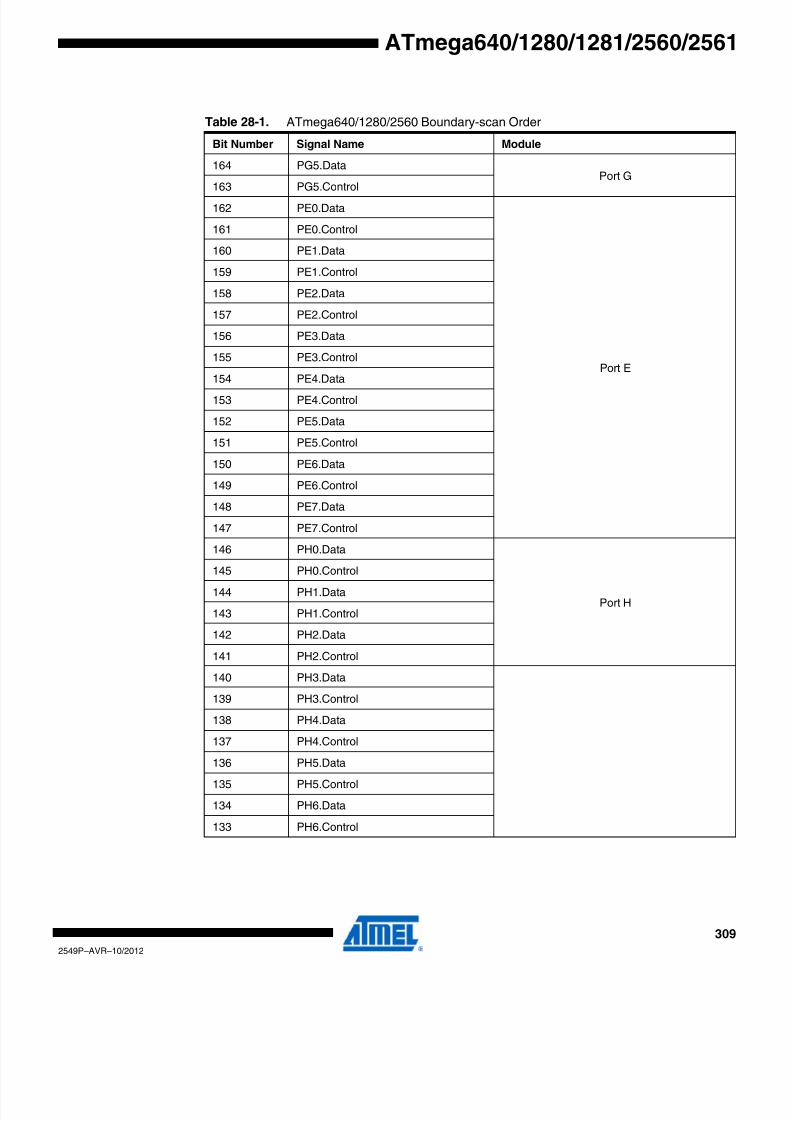
8/20/2019 At Mega 1281 Unlocked
http://slidepdf.com/reader/full/at-mega-1281-unlocked 309/446
309
2549P–AVR–10/2012
ATmega640/1280/1281/2560/2561
Table 28-1. ATmega640/1280/2560 Boundary-scan Order
Bit Number Signal Name Module
164 PG5.DataPort G
163 PG5.Control162 PE0.Data
Port E
161 PE0.Control
160 PE1.Data
159 PE1.Control
158 PE2.Data
157 PE2.Control
156 PE3.Data
155 PE3.Control
154 PE4.Data153 PE4.Control
152 PE5.Data
151 PE5.Control
150 PE6.Data
149 PE6.Control
148 PE7.Data
147 PE7.Control
146 PH0.Data
Port H
145 PH0.Control144 PH1.Data
143 PH1.Control
142 PH2.Data
141 PH2.Control
140 PH3.Data
139 PH3.Control
138 PH4.Data
137 PH4.Control
136 PH5.Data135 PH5.Control
134 PH6.Data
133 PH6.Control
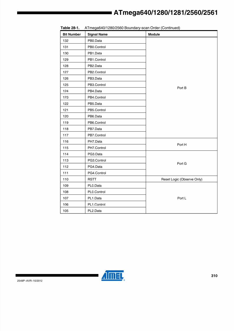
8/20/2019 At Mega 1281 Unlocked
http://slidepdf.com/reader/full/at-mega-1281-unlocked 310/446
310
2549P–AVR–10/2012
ATmega640/1280/1281/2560/2561
132 PB0.Data
Port B
131 PB0.Control
130 PB1.Data
129 PB1.Control
128 PB2.Data
127 PB2.Control
126 PB3.Data
125 PB3.Control
124 PB4.Data
123 PB4.Control
122 PB5.Data
121 PB5.Control
120 PB6.Data
119 PB6.Control
118 PB7.Data
117 PB7.Control
116 PH7.DataPort H
115 PH7.Control
114 PG3.Data
Port G113 PG3.Control
112 PG4.Data
111 PG4.Control
110 RSTT Reset Logic (Observe Only)
109 PL0.Data
Port L
108 PL0.Control
107 PL1.Data
106 PL1.Control
105 PL2.Data
Table 28-1. ATmega640/1280/2560 Boundary-scan Order (Continued)
Bit Number Signal Name Module

8/20/2019 At Mega 1281 Unlocked
http://slidepdf.com/reader/full/at-mega-1281-unlocked 311/446
311
2549P–AVR–10/2012
ATmega640/1280/1281/2560/2561
104 PL2.Control
103 PL3.Data
102 PL3.Control
101 PL4.Data
100 PL4.Control
99 PL5.Data
98 PL5.Control
97 PL6.Data
96 PL6.Control
95 PL7.Data
94 PL7.Control
93 PD0.Data
Port D
92 PD0.Control
91 PD1.Data
90 PD1.Control
89 PD2.Data
88 PD2.Control
87 PD3.Data
86 PD3.Control
85 PD4.Data
84 PD4.Control
83 PD5.Data
82 PD5.Control
81 PD6.Data
80 PD6.Control
79 PD7.Data
78 PD7.Control
77 PG0.Data
Port G76 PG0.Control
75 PG1.Data
74 PG1.Control
73 PC0.Data
Port C
72 PC0.Control
71 PC1.Data
70 PC1.Control
69 PC2.Data
Table 28-1. ATmega640/1280/2560 Boundary-scan Order (Continued)
Bit Number Signal Name Module

8/20/2019 At Mega 1281 Unlocked
http://slidepdf.com/reader/full/at-mega-1281-unlocked 312/446
312
2549P–AVR–10/2012
ATmega640/1280/1281/2560/2561
68 PC2.Control
67 PC3.Data
66 PC3.Control
65 PC4.Data
64 PC4.Control
63 PC5.Data
62 PC5.Control
61 PC6.Data
60 PC6.Control
59 PC7.Data
58 PC7.Control
57 PJ0.Data
Port J
56 PJ0.Control
55 PJ1.Data
54 PJ1.Control
53 PJ2.Data
52 PJ2.Control
51 PJ3.Data
50 PJ3.Control
49 PJ4.Data
48 PJ4.Control
47 PJ5.Data
46 PJ5.Control
45 PJ6.Data
44 PJ6.Control
43 PG2.DataPort G
42 PG2.Control
41 PA7.Data
Port A
40 PA7.Control
39 PA6.Data
38 PA6.Control
37 PA5.Data
36 PA5.Control
35 PA4.Data
34 PA4.Control
33 PA3.Data
Table 28-1. ATmega640/1280/2560 Boundary-scan Order (Continued)
Bit Number Signal Name Module

8/20/2019 At Mega 1281 Unlocked
http://slidepdf.com/reader/full/at-mega-1281-unlocked 313/446
313
2549P–AVR–10/2012
ATmega640/1280/1281/2560/2561
32 PA3.Control
31 PA2.Data
30 PA2.Control
29 PA1.Data
28 PA1.Control
27 PA0.Data
26 PA0.Control
25 PJ7.DataPort J
24 PJ7.Control
23 PK7.Data
Port K
22 PK7.Control
21 PK6.Data
20 PK6.Control
19 PK5.Data
18 PK5.Control
17 PK4.Data
16 PK4.Control
15 PK3.Data
14 PK3.Control
13 PK2.Data
12 PK2.Control
11 PK1.Data
10 PK1.Control
9 PK0.Data
8 PK0.Control
7 PF3.Data
Port F
6 PF3.Control
5 PF2.Data
4 PF2.Control
3 PF1.Data
2 PF1.Control
1 PF0.Data
0 PF0.Control
Table 28-1. ATmega640/1280/2560 Boundary-scan Order (Continued)
Bit Number Signal Name Module

8/20/2019 At Mega 1281 Unlocked
http://slidepdf.com/reader/full/at-mega-1281-unlocked 314/446
314
2549P–AVR–10/2012
ATmega640/1280/1281/2560/2561
Table 28-2. ATmega1281/2561 Boundary-scan Order
Bit Number Signal Name Module
100 PG5.DataPort G
99 PG5.Control
98 PE0.Data
Port E
97 PE0.Control
96 PE1.Data
95 PE1.Control
94 PE2.Data
93 PE2.Control
92 PE3.Data
91 PE3.Control
90 PE4.Data
89 PE4.Control
88 PE5.Data
87 PE5.Control
86 PE6.Data
85 PE6.Control
84 PE7.Data
83 PE7.Control
82 PB0.Data
Port B
81 PB0.Control
80 PB1.Data
79 PB1.Control
78 PB2.Data
77 PB2.Control
76 PB3.Data
75 PB3.Control
74 PB4.Data
73 PB4.Control
72 PB5.Data
71 PB5.Control
70 PB6.Data
69 PB6.Control
68 PB7.Data
67 PB7.Control
66 PG3.Data Port G

8/20/2019 At Mega 1281 Unlocked
http://slidepdf.com/reader/full/at-mega-1281-unlocked 315/446
315
2549P–AVR–10/2012
ATmega640/1280/1281/2560/2561
65 PG3.Control
64 PG4.Data
63 PG4.Control
62 RSTT Reset Logic (Observe Only)
61 PD0.Data
Port D
60 PD0.Control
59 PD1.Data
58 PD1.Control
57 PD2.Data
56 PD2.Control
55 PD3.Data
54 PD3.Control
53 PD4.Data
52 PD4.Control
51 PD5.Data
50 PD5.Control
49 PD6.Data
48 PD6.Control
47 PD7.Data
46 PD7.Control
45 PG0.Data
Port G44 PG0.Control
43 PG1.Data
42 PG1.Control
41 PC0.Data
Port C
40 PC0.Control
39 PC1.Data
38 PC1.Control
37 PC2.Data
36 PC2.Control
35 PC3.Data
34 PC3.Control
33 PC4.Data
32 PC4.Control
31 PC5.Data
30 PC5.Control
Table 28-2. ATmega1281/2561 Boundary-scan Order (Continued)
Bit Number Signal Name Module

8/20/2019 At Mega 1281 Unlocked
http://slidepdf.com/reader/full/at-mega-1281-unlocked 316/446
316
2549P–AVR–10/2012
ATmega640/1280/1281/2560/2561
29 PC6.Data
28 PC6.Control
27 PC7.Data
26 PC7.Control
25 PG2.DataPort G
24 PG2.Control
23 PA7.Data
Port A
22 PA7.Control
21 PA6.Data
20 PA6.Control
19 PA5.Data
18 PA5.Control
17 PA4.Data
16 PA4.Control
15 PA3.Data
14 PA3.Control
13 PA2.Data
12 PA2.Control
11 PA1.Data
10 PA1.Control
9 PA0.Data
8 PA0.Control
7 PF3.Data
Port F
6 PF3.Control
5 PF2.Data
4 PF2.Control
3 PF1.Data
2 PF1.Control
1 PF0.Data
0 PF0.Control
Table 28-2. ATmega1281/2561 Boundary-scan Order (Continued)
Bit Number Signal Name Module

8/20/2019 At Mega 1281 Unlocked
http://slidepdf.com/reader/full/at-mega-1281-unlocked 317/446
317
2549P–AVR–10/2012
ATmega640/1280/1281/2560/2561
29. Boot Loader Support – Read-While-Write Self-ProgrammingThe Boot Loader Support provides a real Read-While-Write Self-Programming mechanism fo
downloading and uploading program code by the MCU itself. This feature allows flexible applica-
tion software updates controlled by the MCU using a Flash-resident Boot Loader program. The
Boot Loader program can use any available data interface and associated protocol to read code
and write (program) that code into the Flash memory, or read the code from the program mem-
ory. The program code within the Boot Loader section has the capability to write into the entire
Flash, including the Boot Loader memory. The Boot Loader can thus even modify itself, and it
can also erase itself from the code if the feature is not needed anymore. The size of the Boo
Loader memory is configurable with fuses and the Boot Loader has two separate sets of Boo
Lock bits which can be set independently. This gives the user a unique flexibility to select differ
ent levels of protection.
29.1 Features• Read-While-Write Self-Programming
• Flexible Boot Memory Size
• High Security (Separate Boot Lock Bits for a Flexible Protection)
• Separate Fuse to Select Reset Vector• Optimized Page(1) Size
• Code Efficient Algorithm
• Efficient Read-Modify-Write Support
Note: 1. A page is a section in the Flash consisting of several bytes (see Table 30-7 on page 338) usedduring programming. The page organization does not affect normal operation.
29.2 Application and Boot Loader Flash Sections
The Flash memory is organized in two main sections, the Application section and the Boo
Loader section (see Figure 29-2 on page 320). The size of the different sections is configured by
the BOOTSZ Fuses as shown in Table 29-7 on page 328 and Figure 29-2 on page 320. These
two sections can have different level of protection since they have different sets of Lock bits.
29.2.1 Application Section
The Application section is the section of the Flash that is used for storing the application code.
The protection level for the Application section can be selected by the application Boot Lock bits
(Boot Lock bits 0), see Table 29-2 on page 321. The Application section can never store any
Boot Loader code since the SPM instruction is disabled when executed from the Application
section.
29.2.2 BLS – Boot Loader Section
While the Application section is used for storing the application code, the The Boot Loader soft-
ware must be located in the BLS since the SPM instruction can initiate a programming when
executing from the BLS only. The SPM instruction can access the entire Flash, including theBLS itself. The protection level for the Boot Loader section can be selected by the Boot Loader
Lock bits (Boot Lock bits 1), see Table 29-3 on page 321.
29.3 Read-While-Write and No Read-While-Write Flash Sections
Whether the CPU supports Read-While-Write or if the CPU is halted during a Boot Loader soft-
ware update is dependent on which address that is being programmed. In addition to the two
sections that are configurable by the BOOTSZ Fuses as described above, the Flash is also

8/20/2019 At Mega 1281 Unlocked
http://slidepdf.com/reader/full/at-mega-1281-unlocked 318/446
318
2549P–AVR–10/2012
ATmega640/1280/1281/2560/2561
divided into two fixed sections, the Read-While-Write (RWW) section and the No Read-While
Write (NRWW) section. The limit between the RWW- and NRWW sections is given in Table 29
1 and Figure 29-1 on page 319. The main difference between the two sections is:
• When erasing or writing a page located inside the RWW section, the NRWW section can beread during the operation
• W
hen erasing or writing a page located inside theN
RWW
section, the CPU is halted duringthe entire operation
Note that the user software can never read any code that is located inside the RWW section dur
ing a Boot Loader software operation. The syntax “Read-While-Write section” refers to which
section that is being programmed (erased or written), not which section that actually is being
read during a Boot Loader software update.
29.3.1 RWW – Read-While-Write Section
If a Boot Loader software update is programming a page inside the R WW section, it is possible
to read code from the Flash, but only code that is located in the NRWW section. During an on
going programming, the software must ensure that the RWW section never is being read. If the
user software is trying to read code that is located inside the RWW section (that is, by load pro
gram memory, call, or jump instructions or an interrupt) during programming, the software mightend up in an unknown state. To avoid this, the interrupts should either be disabled or moved to
the Boot Loader section. The Boot Loader section is always located in the NRWW section. The
RWW Section Busy bit (RWWSB) in the Store Program Memory Control and Status Registe
(SPMCSR) will be read as logical one as long as the R WW section is blocked for reading. Afte
a programming is completed, the RWWSB must be cleared by software before reading code
located in the RWW section. See “SPMCSR – Store Program Memory Control and Status Reg-
ister” on page 332. for details on how to clear RWWSB.
29.3.2 NRWW – No Read-While-Write Section
The code located in the NRWW section can be read when the Boot Loader software is updating
a page in the RWW section. When the Boot Loader code updates the NRWW section, the CPU
is halted during the entire Page Erase or Page Write operation.
Table 29-1. Read-While-Write Features
Which Section does the Z-pointer
Address during the Programming?
Which Section can be
Read during Programming? CPU Halted?
Read-While-Write
Supported?
RWW Section NRWW Section No Yes
NRWW Section None Yes No
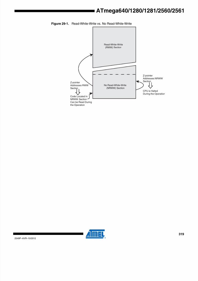
8/20/2019 At Mega 1281 Unlocked
http://slidepdf.com/reader/full/at-mega-1281-unlocked 319/446
319
2549P–AVR–10/2012
ATmega640/1280/1281/2560/2561
Figure 29-1. Read-While-Write vs. No Read-While-Write
Read-While-Write
(RWW) Section
No Read-While-Write(NRWW) Section
Z-pointerAddresses RWWSection
Z-pointerAddresses NRWWSection
CPU is HaltedDuring the Operation
Code Located inNRWW SectionCan be Read Duringthe Operation

8/20/2019 At Mega 1281 Unlocked
http://slidepdf.com/reader/full/at-mega-1281-unlocked 320/446
320
2549P–AVR–10/2012
ATmega640/1280/1281/2560/2561
Figure 29-2. Memory Sections
Note: 1. The parameters in the figure above are given in Table 29-7 on page 328.
29.4 Boot Loader Lock Bits
If no Boot Loader capability is needed, the entire Flash is available for application code. The
Boot Loader has two separate sets of Boot Lock bits which can be set independently. This gives
the user a unique flexibility to select different levels of protection.
The user can select:
• To protect the entire Flash from a software update by the MCU
• To protect only the Boot Loader Flash section from a software update by the MCU• To protect only the Application Flash section from a software update by the MCU
• Allow software update in the entire Flash
See Table 29-2 on page 321 and Table 29-3 on page 321 for further details. The Boot Lock bits
can be set in software and in Serial or Parallel Programming mode, but they can be cleared by a
Chip Erase command only. The general Write Lock (Lock Bit mode 2) does not control the pro
gramming of the Flash memory by SPM instruction. Similarly, the general Read/ Write Lock
(Lock Bit mode 1) does not control reading nor writing by (E)LPM/SPM, if it is attempted.
0x0000
Flashend
Program Memory
BOOTSZ = '11'
Application Flash Section
Boot Loader Flash SectionFlashend
Program Memory
BOOTSZ = '10'
0x0000
Program Memory
BOOTSZ = '01'
Program Memory
BOOTSZ = '00'
Application Flash Section
Boot Loader Flash Section
0x0000
Flashend
Application Flash Section
Flashend
End RWW
Start NRWW
Application Flash Section
Boot Loader Flash Section
Boot Loader Flash Section
End RWW
Start NRWW
End RWW
Start NRWW
0x0000
End RWW, End Application
Start NRWW, Start Boot Loader
Application Flash SectionApplication Flash Section
Application Flash Section
R e a d - W h i l e - W r i t e S e c t i o n
N o R e a d - W h i l e - W r i t e S e c t i o n
R e a d - W h i l e - W r i t e S e c t i o n
N o R e a d - W h i l e - W r i t e S e c t i o n
R e a d - W h i l e -
W r i t e S e c t i o n
N o R e a d - W h i l e - W r i t e S e c t i o n
R e a d - W h i l e - W r i t e S e c t i o n
N o R e a d - W h i l e - W r i t e S e c t i o n
End Application
Start Boot Loader
End Application
Start Boot Loader
End Application
Start Boot Loader

8/20/2019 At Mega 1281 Unlocked
http://slidepdf.com/reader/full/at-mega-1281-unlocked 321/446
321
2549P–AVR–10/2012
ATmega640/1280/1281/2560/2561
Note: 1. “1” means unprogrammed, “0” means programmed.
Note: 1. “1” means unprogrammed, “0” means programmed.
29.4.1 Entering the Boot Loader Program
Entering the Boot Loader takes place by a jump or call from the application program. This may
be initiated by a trigger such as a command received via USART, or SPI interface. Alternatively
the Boot Reset Fuse can be programmed so that the Reset Vector is pointing to the Boot Flash
start address after a reset. In this case, the Boot Loader is started after a reset. After the applica-
tion code is loaded, the program can start executing the application code. Note that the fuses
cannot be changed by the MCU itself. This means that once the Boot Reset Fuse is pro
grammed, the Reset Vector will always point to the Boot Loader Reset and the fuse can only be
changed through the serial or parallel programming interface.
Note: 1. “1” means unprogrammed, “0” means programmed.
Table 29-2. Boot Lock Bit0 Protection Modes (Application Section)(1)
BLB0 Mode BLB02 BLB01 Protection
1 1 1 No restrictions for SPM or (E)LPM accessing the Application
section.
2 1 0 SPM is not allowed to write to the Application section.
3 0 0
SPM is not allowed to write to the Application section, and(E)LPM executing from the Boot Loader section is not allowed toread from the Application section. If Interrupt Vectors are placedin the Boot Loader section, interrupts are disabled whileexecuting from the Application section.
4 0 1
(E)LPM executing from the Boot Loader section is not allowed toread from the Application section. If Interrupt Vectors are placedin the Boot Loader section, interrupts are disabled whileexecuting from the Application section.
Table 29-3. Boot Lock Bit1 Protection Modes (Boot Loader Section)(1)
BLB1 Mode BLB12 BLB11 Protection
1 1 1 No restrictions for SPM or (E)LPM accessing the Boot Loader
section.
2 1 0 SPM is not allowed to write to the Boot Loader section.
3 0 0
SPM is not allowed to write to the Boot Loader section, and(E)LPM executing from the Application section is not allowed toread from the Boot Loader section. If Interrupt Vectors areplaced in the Application section, interrupts are disabled whileexecuting from the Boot Loader section.
4 0 1
(E)LPM executing from the Application section is not allowed toread from the Boot Loader section. If Interrupt Vectors are
placed in the Application section, interrupts are disabled whileexecuting from the Boot Loader section.
Table 29-4. Boot Reset Fuse(1)
BOOTRST Reset Address
1 Reset Vector = Application Reset (address 0x0000)
0 Reset Vector = Boot Loader Reset (see Table 29-7 on page 328)

8/20/2019 At Mega 1281 Unlocked
http://slidepdf.com/reader/full/at-mega-1281-unlocked 322/446
322
2549P–AVR–10/2012
ATmega640/1280/1281/2560/2561
29.5 Addressing the Flash During Self-Programming
The Z-pointer is used to address the SPM commands. The Z pointer consists of the Z-registers
ZL and ZH in the register file, and RAMPZ in the I/O space. The number of bits actually used is
implementation dependent. Note that the RAMPZ register is only implemented when the pro
gram space is larger than 64Kbytes.
Since the Flash is organized in pages (see Table 30-7 on page 338), the Program Counter can
be treated as having two different sections. One section, consisting of the least significant bits, is
addressing the words within a page, while the most significant bits are addressing the pages
This is shown in Figure 29-3. Note that the Page Erase and Page Write operations are
addressed independently. Therefore it is of major importance that the Boot Loader software
addresses the same page in both the Page Erase and Page Write operation. Once a program-
ming operation is initiated, the address is latched and the Z-pointer can be used for otheoperations.
The (E)LPM instruction use the Z-pointer to store the address. Since this instruction addresses
the Flash byte-by-byte, also bit Z0 of the Z-pointer is used.
Figure 29-3. Addressing the Flash During SPM(1)
Note: 1. The different variables used in Figure 29-3 are listed in Table 29-9 on page 329.
Bit 23 22 21 20 19 18 17 16
15 14 13 12 11 10 9 8
RAMPZ RAMPZ7 RAMPZ6 RAMPZ5 RAMPZ4 RAMPZ3 RAMPZ2 RAMPZ1 RAMPZ0
ZH (R31) Z15 Z14 Z13 Z12 Z11 Z10 Z9 Z8
ZL (R30) Z7 Z6 Z5 Z4 Z3 Z2 Z1 Z0
7 6 5 4 3 2 1 0
PROGRAM MEMORY
0115
Z - REGISTER
BIT
0
ZPAGEMSB
WORD ADDRESSWITHIN A PAGE
PAGE ADDRESSWITHIN THE FLASH
ZPCMSB
INSTRUCTION WORD
PAGE PCWORD[PAGEMSB:0]:
00
01
02
PAGEEND
PAGE
PCWORDPCPAGE
PCMSB PAGEMSBPROGRAMCOUNTER

8/20/2019 At Mega 1281 Unlocked
http://slidepdf.com/reader/full/at-mega-1281-unlocked 323/446
323
2549P–AVR–10/2012
ATmega640/1280/1281/2560/2561
29.6 Self-Programming the Flash
The program memory is updated in a page by page fashion. Before programming a page with
the data stored in the temporary page buffer, the page must be erased. The temporary page buf
fer is filled one word at a time using SPM and the buffer can be filled either before the Page
Erase command or between a Page Erase and a Page Write operation:
Alternative 1, fill the buffer before a Page Erase• Fill temporary page buffer
• Perform a Page Erase
• Perform a Page Write
Alternative 2, fill the buffer after Page Erase
• Perform a Page Erase
• Fill temporary page buffer
• Perform a Page Write
If only a part of the page needs to be changed, the rest of the page must be stored (for example
in the temporary page buffer) before the erase, and then be rewritten. When using alternative 1
the Boot Loader provides an effective Read-Modify-Write feature which allows the user softwareto first read the page, do the necessary changes, and then write back the modified data. If alter
native 2 is used, it is not possible to read the old data while loading since the page is already
erased. The temporary page buffer can be accessed in a random sequence. It is essential that
the page address used in both the Page Erase and Page Write operation is addressing the same
page. See “Simple Assembly Code Example for a Boot Loader” on page 327 for an assembly
code example.
29.6.1 Performing Page Erase by SPM
To execute Page Erase, set up the address in the Z-pointer, write “X0000011” to SPMCSR and
execute SPM within four clock cycles after writing SPMCSR. The data in R1 and R0 is ignored
The page address must be written to PCPAGE in the Z-register. Other bits in the Z-pointer wil
be ignored during this operation.
• Page Erase to the RWW section: The NRWW section can be read during the Page Erase
• Page Erase to the NRWW section: The CPU is halted during the operation
29.6.2 Filling the Temporary Buffer (Page Loading)
To write an instruction word, set up the address in the Z-pointer and data in R1:R0, write
“00000001” to SPMCSR and execute SPM within four clock cycles after writing SPMCSR. The
content of PCWORD in the Z-register is used to address the data in the temporary buffer. The
temporary buffer will auto-erase after a Page Write operation or by writing the RWWSRE bit in
SPMCSR. It is also erased after a system reset. Note that it is not possible to write more than
one time to each address without erasing the temporary buffer.
If the EEPROM is written in the middle of an SPM Page Load operation, all data loaded is stil
buffered.

8/20/2019 At Mega 1281 Unlocked
http://slidepdf.com/reader/full/at-mega-1281-unlocked 324/446
324
2549P–AVR–10/2012
ATmega640/1280/1281/2560/2561
29.6.3 Performing a Page Write
To execute Page Write, set up the address in the Z-pointer, write “X0000101” to SPMCSR and
execute SPM within four clock cycles after writing SPMCSR. The data in R1 and R0 is ignored
The page address must be written to PCPAGE. Other bits in the Z-pointer must be written to
zero during this operation.
• Page Write to the RWW section: The NRWW section can be read during the Page Write
• Page Write to the NRWW section: The CPU is halted during the operation
29.6.4 Using the SPM Interrupt
If the SPM interrupt is enabled, the SPM interrupt will generate a constant interrupt when the
SPMEN bit in SPMCSR is cleared. This means that the interrupt can be used instead of polling
the SPMCSR Register in software. When using the SPM interrupt, the Interrupt Vectors should
be moved to the BLS section to avoid that an interrupt is accessing the RWW section when it is
blocked for reading. How to move the interrupts is described in “Interrupts” on page 105.
29.6.5 Consideration While Updating BLSSpecial care must be taken if the user allows the Boot Loader section to be updated by leaving
Boot Lock bit11 unprogrammed. An accidental write to the Boot Loader itself can corrupt the
entire Boot Loader, and further software updates might be impossible. If it is not necessary to
change the Boot Loader software itself, it is recommended to program the Boot Lock bit11 to
protect the Boot Loader software from any internal software changes.
29.6.6 Prevent Reading the RWW Section During Self-Programming
During Self-Programming (either Page Erase or Page Write), the RWW section is always
blocked for reading. The user software itself must prevent that this section is addressed during
the self programming operation. The RWWSB in the SPMCSR will be set as long as the RWW
section is busy. During Self-Programming the Interrupt Vector table should be moved to the BLS
as described in “Interrupts” on page 105, or the interrupts must be disabled. Before addressingthe RWW section after the programming is completed, the user software must clear the
RWWSB by writing the RWWSRE. See “Simple Assembly Code Example for a Boot Loader” on
page 327 for an example.
29.6.7 Setting the Boot Loader Lock Bits by SPM
To set the Boot Loader Lock bits and general Lock bits, write the desired data to R0, write
“X0001001” to SPMCSR and execute SPM within four clock cycles after writing SPMCSR.
See Table 29-2 on page 321 and Table 29-3 on page 321 for how the different settings of the
Boot Loader bits affect the Flash access.
If bits 5:0 in R0 are cleared (zero), the corresponding Lock bit will be programmed if an SPM
instruction is executed within four cycles after BLBSET and SPMEN are set in SPMCSR. The Z-
pointer is don’t care during this operation, but for future compatibility it is recommended to load
the Z-pointer with 0x0001 (same as used for reading the lO ck bits). For future compatibility it is
also recommended to set bits 7 and 6 in R0 to “1” when writing the Lock bits. When program
ming the Lock bits the entire Flash can be read during the operation.
Bit 7 6 5 4 3 2 1 0
R0 1 1 BLB12 BLB11 BLB02 BLB01 LB2 LB1

8/20/2019 At Mega 1281 Unlocked
http://slidepdf.com/reader/full/at-mega-1281-unlocked 325/446
325
2549P–AVR–10/2012
ATmega640/1280/1281/2560/2561
29.6.8 EEPROM Write Prevents Writing to SPMCSR
Note that an EEPROM write operation will block all software programming to Flash. Reading the
Fuses and Lock bits from software will also be prevented during the EEPROM write operation. I
is recommended that the user checks the status bit (EEPE) in the EECR Register and verifies
that the bit is cleared before writing to the SPMCSR Register.
29.6.9 Reading the Fuse and Lock Bits from SoftwareIt is possible to read both the Fuse and Lock bits from software. To read the Lock bits, load the
Z-pointer with 0x0001 and set the BLBSET and SPMEN bits in SPMCSR. When an (E)LPM
instruction is executed within three CPU cycles after the BLBSET and SPMEN bits are set in
SPMCSR, the value of the Lock bits will be loaded in the destination register. The BLBSET and
SPMEN bits will auto-clear upon completion of reading the Lock bits or if no (E)LPM instruction
is executed within three CPU cycles or no SPM instruction is executed within four CPU cycles
When BLBSET and SPMEN are cleared, (E)LPM will work as described in the Instruction se
Manual.
The algorithm for reading the Fuse Low byte is similar to the one described above for readingthe Lock bits. To read the Fuse Low byte, load the Z-pointer with 0x0000 and set the BLBSET
and SPMEN bits in SPMCSR. When an (E)LPM instruction is executed within three cycles afte
the BLBSET and SPMEN bits are set in the SPMCSR, the value of the Fuse Low byte (FLB) wil
be loaded in the destination register as shown below. Refer to Table 30-5 on page 337 for a
detailed description and mapping of the Fuse Low byte.
Similarly, when reading the Fuse High byte, load 0x0003 in the Z-pointer. When an (E)LPM
instruction is executed within three cycles after the BLBSET and SPMEN bits are set in the
SPMCSR, the value of the Fuse High byte (FHB) will be loaded in the destination register as
shown below. Refer to Table 30-4 on page 337 for detailed description and mapping of the FuseHigh byte.
When reading the Extended Fuse byte, load 0x0002 in the Z-pointer. When an (E)LPM instruc
tion is executed within three cycles after the BLBSET and SPMEN bits are set in the SPMCSR
the value of the Extended Fuse byte (EFB) will be loaded in the destination register as shown
below. Refer to Table 30-3 on page 336 for detailed description and mapping of the Extended
Fuse byte.
Fuse and Lock bits that are programmed, will be read as zero. Fuse and Lock bits that are
unprogrammed, will be read as one.
29.6.10 Reading the Signature Row from Software
To read the Signature Row from software, load the Z-pointer with the signature byte address
given in Table 29-5 on page 326 and set the SIGRD and SPMEN bits in SPMCSR. When an
LPM instruction is executed within three CPU cycles after the SIGRD and SPMEN bits are set in
Bit 7 6 5 4 3 2 1 0
Rd – – BLB12 BLB11 BLB02 BLB01 LB2 LB1
Bit 7 6 5 4 3 2 1 0
Rd FLB7 FLB6 FLB5 FLB4 FLB3 FLB2 FLB1 FLB0
Bit 7 6 5 4 3 2 1 0
Rd FHB7 FHB6 FHB5 FHB4 FHB3 FHB2 FHB1 FHB0
Bit 7 6 5 4 3 2 1 0
Rd – – – – – EFB2 EFB1 EFB0

8/20/2019 At Mega 1281 Unlocked
http://slidepdf.com/reader/full/at-mega-1281-unlocked 326/446
326
2549P–AVR–10/2012
ATmega640/1280/1281/2560/2561
SPMCSR, the signature byte value will be loaded in the destination register. The SIGRD and
SPMEN bits will auto-clear upon completion of reading the Signature Row Lock bits or if no LPM
instruction is executed within three CPU cycles. When SIGRD and SPMEN are cleared, LPM wil
work as described in the Instruction set Manual.
Note: All other addresses are reserved for future use.
29.6.11 Preventing Flash Corruption
During periods of low VCC, the Flash program can be corrupted because the supply voltage is
too low for the CPU and the Flash to operate properly. These issues are the same as for board
level systems using the Flash, and the same design solutions should be applied.
A Flash program corruption can be caused by two situations when the voltage is too low. First, a
regular write sequence to the Flash requires a minimum voltage to operate correctly. Secondly,
the CPU itself can execute instructions incorrectly, if the supply voltage for executing instructions
is too low.
Flash corruption can easily be avoided by following these design recommendations (one is
sufficient):
1. If there is no need for a Boot Loader update in the system, program the Boot Loader Lockbits to prevent any Boot Loader software updates.
2. Keep the AVR RESET active (low) during periods of insufficient power supply voltage.
This can be done by enabling the internal Brown-out Detector (BOD) if the operating volt-age matches the detection level. If not, an external low VCC reset protection circuit can beused. If a reset occurs while a write operation is in progress, the write operation will becompleted provided that the power supply voltage is sufficient.
3. Keep the AVR core in Power-down sleep mode during periods of low VCC. This will pre-vent the CPU from attempting to decode and execute instructions, effectively protectingthe SPMCSR Register and thus the Flash from unintentional writes.
29.6.12 Programming Time for Flash when Using SPM
The calibrated RC Oscillator is used to time Flash accesses. Table 29-6 shows the typical pro
gramming time for Flash accesses from the CPU.
Table 29-5. Signature Row Addressing
Signature Byte Z-Pointer Address
Device Signature Byte 1 0x0000
Device Signature Byte 2 0x0002
Device Signature Byte 3 0x0004
RC Oscillator Calibration Byte 0x0001
Table 29-6. SPM Programming TimeSymbol Min Programming Time Max Programming Time
Flash write (Page Erase, Page Write, andwrite Lock bits by SPM)
3.7ms 4.5ms

8/20/2019 At Mega 1281 Unlocked
http://slidepdf.com/reader/full/at-mega-1281-unlocked 327/446
327
2549P–AVR–10/2012
ATmega640/1280/1281/2560/2561
29.6.13 Simple Assembly Code Example for a Boot Loader;-the routine writes one page of data from RAM to Flash; the first data location in RAM is pointed to by the Y pointer; the first data location in Flash is pointed to by the Z-pointer;-error handling is not included;-the routine must be placed inside the Boot space; (at least the Do_spm sub routine). Only code inside NRWW section can
; be read during Self-Programming (Page Erase and Page Write).;-registers used: r0, r1, temp1 (r16), temp2 (r17), looplo (r24),; loophi (r25), spmcrval (r20); storing and restoring of registers is not included in the routine; register usage can be optimized at the expense of code size;-It is assumed that either the interrupt table is moved to the Boot; loader section or that the interrupts are disabled.
.equ PAGESIZEB = PAGESIZE*2 ;PAGESIZEB is page size in BYTES, not words
.org SMALLBOOTSTART Write_page:
; Page Eraseldi spmcrval, (1<<PGERS) | (1<<SPMEN)call Do_spm
; re-enable the RWW sectionldi spmcrval, (1<<RWWSRE) | (1<<SPMEN)call Do_spm
; transfer data from RAM to Flash page bufferldi looplo, low(PAGESIZEB) ;init loop variableldi loophi, high(PAGESIZEB) ;not required for PAGESIZEB<=256
Wrloop:ld r0, Y+ld r1, Y+ldi spmcrval, (1<<SPMEN)call Do_spm adiw ZH:ZL, 2sbiw loophi:looplo, 2 ;use subi for PAGESIZEB<=256
brne Wrloop
; execute Page Writesubi ZL, low(PAGESIZEB) ;restore pointersbci ZH, high(PAGESIZEB) ;not required for PAGESIZEB<=256ldi spmcrval, (1<<PGWRT) | (1<<SPMEN)call Do_spm
; re-enable the RWW sectionldi spmcrval, (1<<RWWSRE) | (1<<SPMEN)call Do_spm
; read back and check, optionalldi looplo, low(PAGESIZEB) ;init loop variableldi loophi, high(PAGESIZEB) ;not required for PAGESIZEB<=256subi YL, low(PAGESIZEB) ;restore pointersbci YH, high(PAGESIZEB)
Rdloop:elpm r0, Z+ld r1, Y+cpse r0, r1jmp Errorsbiw loophi:looplo, 1 ;use subi for PAGESIZEB<=256brne Rdloop
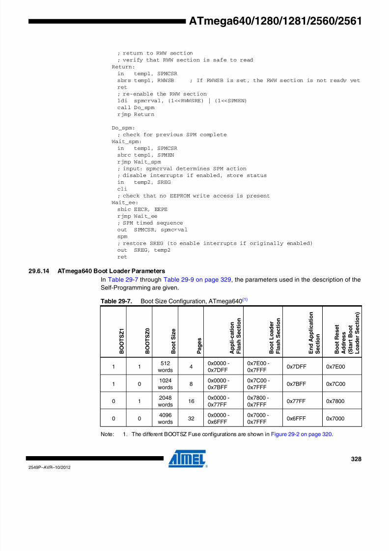
8/20/2019 At Mega 1281 Unlocked
http://slidepdf.com/reader/full/at-mega-1281-unlocked 328/446
328
2549P–AVR–10/2012
ATmega640/1280/1281/2560/2561
; return to RWW section; verify that RWW section is safe to read
Return:in temp1, SPMCSRsbrs temp1, RWWSB ; If RWWSB is set, the RWW section is not ready yetret
; re-enable the RWW sectionldi spmcrval, (1<<RWWSRE) | (1<<SPMEN)call Do_spm rjmp Return
Do_spm:; check for previous SPM complete
Wait_spm:in temp1, SPMCSRsbrc temp1, SPMENrjmp Wait_spm ; input: spmcrval determines SPM action; disable interrupts if enabled, store statusin temp2, SREG
cli; check that no EEPROM write access is present
Wait_ee:sbic EECR, EEPErjmp Wait_ee; SPM timed sequenceout SPMCSR, spmcrvalspm ; restore SREG (to enable interrupts if originally enabled)out SREG, temp2ret
29.6.14 ATmega640 Boot Loader Parameters
In Table 29-7 through Table 29-9 on page 329, the parameters used in the description of theSelf-Programming are given.
Note: 1. The different BOOTSZ Fuse configurations are shown in Figure 29-2 on page 320.
Table 29-7. Boot Size Configuration, ATmega640(1)
B O O T S Z 1
B O O T S Z 0
B o o t S i z e
P a g e s
A p p l i - c a t i o n
F l a s h S e c t i o n
B o o t L o a d e r
F l a s h S e c t i o n
E n d A p p l i c a t i o n
S e c t i o n
B o o t R e s e t
A d d r e s s
( S t a r t B o o t
L o a d e r S e c t i o n )
1 1512
words4
0x0000 -0x7DFF
0x7E00 -0x7FFF
0x7DFF 0x7E00
1 01024words
80x0000 -0x7BFF
0x7C00 -0x7FFF
0x7BFF 0x7C00
0 12048words
160x0000 -0x77FF
0x7800 -0x7FFF
0x77FF 0x7800
0 04096words
320x0000 -0x6FFF
0x7000 -0x7FFF
0x6FFF 0x7000

8/20/2019 At Mega 1281 Unlocked
http://slidepdf.com/reader/full/at-mega-1281-unlocked 329/446
329
2549P–AVR–10/2012
ATmega640/1280/1281/2560/2561
Note: 1. For details about these two section, see “NRWW – No Read-While-Write Section” on page318 and “RWW – Read-While-Write Section” on page 318.
Note: 1. Z0: should be zero for all SPM commands, byte select for the (E)LPM instruction.
2. See “Addressing the Flash During Self-Programming” on page 322 for details about the use ofZ-pointer during Self-Programming.
Table 29-8. Read-While-Write Limit, ATmega640
Section(1) Pages Address
Read-While-Write section (RWW) 224 0x0000 - 0x6FFF
No Read-While-Write section (NRWW) 32 0x7000 - 0x7FFF
Table 29-9. Explanation of different variables used in Figure 29-3 on page 322 and the map-ping to the Z-pointer, ATmega640
Variable
Corresponding
Z-value(2) Description(1)
PCMSB 14Most significant bit in the Program Counter.(The Program Counter is 15 bits PC[14:0]).
PAGEMSB 6
Most significant bit which is used to address
the words within one page (128 words in apage requires seven bits PC [6:0]).
ZPCMSB Z15Bit in Z-pointer that is mapped to PCMSB.Because Z0 is not used, the ZPCMSB equalsPCMSB + 1.
ZPAGEMSB Z7Bit in Z-pointer that is mapped to PCMSB.Because Z0 is not used, the ZPAGEMSBequals PAGEMSB + 1.
PCPAGE PC[14:7] Z15:Z8Program Counter page address: Page select,for Page Erase and Page Write.
PCWORD PC[6:0] Z7:Z1Program Counter word address: Word select,for filling temporary buffer (must be zeroduring Page Write operation).

8/20/2019 At Mega 1281 Unlocked
http://slidepdf.com/reader/full/at-mega-1281-unlocked 330/446
330
2549P–AVR–10/2012
ATmega640/1280/1281/2560/2561
29.6.15 ATmega1280/1281 Boot Loader Parameters
In Table 29-10 and Table 29-11, the parameters used in the description of the Self-Programming
are given.
Note: 1. The different BOOTSZ Fuse configurations are shown in Figure 29-2 on page 320.
Note: 1. For details about these two section, see “NRWW – No Read-While-Write Section” on page318 and “RWW – Read-While-Write Section” on page 318.
Table 29-10. Boot Size Configuration, ATmega1280/1281(1)
B O O T S Z 1
B O O T S Z 0
B o o t S i z e
P a g e s
A p p l i - c a t i o n
F l a s h S e c t i o n
B o o t L o a d e r
F l a s h S e c t i o n
E n d A p p l i c a t i o n
S e c t i o n
B o o t R e s e t A d d r e
s s
( S t a r t B o o t L o a d e
r
S e c t i o n )
1 1512
words4
0x0000 -0xFDFF
0xFE00 -0xFFFF
0xFDFF 0xFE00
1 01024words
80x0000 -0xFBFF
0xFC00 -0xFFFF
0xFBFF 0xFC00
0 1
2048
words 16
0x0000 -
0xF7FF
0xF800 -
0xFFFF 0xF7FF 0xF800
0 04096words
320x0000 -0xEFFF
0xF000 -0xFFFF
0xEFFF 0xF000
Table 29-11. Read-While-Write Limit, ATmega1280/1281
Section(1) Pages Address
Read-While-Write section (RWW) 480 0x0000 - 0xEFFF
No Read-While-Write section (NRWW) 32 0xF000 - 0xFFFF
Table 29-12. Explanation of different variables used in Figure 29-3 on page 322 and the map-ping to the Z-pointer, ATmega1280/1281
Variable
Corresponding
Z-value(2) Description(1)
PCMSB 15Most significant bit in the Program Counter. (TheProgram Counter is 16 bits PC[15:0])
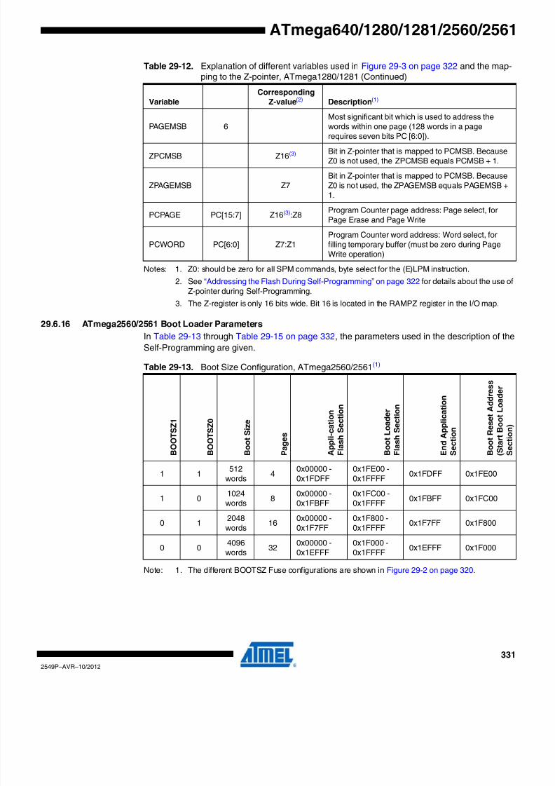
8/20/2019 At Mega 1281 Unlocked
http://slidepdf.com/reader/full/at-mega-1281-unlocked 331/446
331
2549P–AVR–10/2012
ATmega640/1280/1281/2560/2561
Notes: 1. Z0: should be zero for all SPM commands, byte select for the (E)LPM instruction.2. See “Addressing the Flash During Self-Programming” on page 322 for details about the use of
Z-pointer during Self-Programming.
3. The Z-register is only 16 bits wide. Bit 16 is located in the RAMPZ register in the I/O map.
29.6.16 ATmega2560/2561 Boot Loader Parameters
In Table 29-13 through Table 29-15 on page 332, the parameters used in the description of the
Self-Programming are given.
Note: 1. The different BOOTSZ Fuse configurations are shown in Figure 29-2 on page 320.
PAGEMSB 6Most significant bit which is used to address thewords within one page (128 words in a page
requires seven bits PC [6:0]).
ZPCMSB Z16(3) Bit in Z-pointer that is mapped to PCMSB. BecauseZ0 is not used, the ZPCMSB equals PCMSB + 1.
ZPAGEMSB Z7Bit in Z-pointer that is mapped to PCMSB. BecauseZ0 is not used, the ZPAGEMSB equals PAGEMSB +1.
PCPAGE PC[15:7] Z16(3):Z8Program Counter page address: Page select, forPage Erase and Page Write
PCWORD PC[6:0] Z7:Z1Program Counter word address: Word select, forfilling temporary buffer (must be zero during PageWrite operation)
Table 29-12. Explanation of different variables used in Figure 29-3 on page 322 and the map-ping to the Z-pointer, ATmega1280/1281 (Continued)
Variable
Corresponding
Z-value(2) Description(1)
Table 29-13. Boot Size Configuration, ATmega2560/2561(1)
B O O T S Z 1
B O O T S Z 0
B o o t S i z e
P a g e s
A p p l i - c a t i o n
F l a s h S e c t i o n
B o o t L o a d e r
F l a s h S e c t i o n
E n d A p p l i c a t i o
n
S e c t i o n
B o o t R e s e t A d d r e s s
( S t a r t B o o t L o a d e r
S e c t i o n )
1 1512
words4
0x00000 -0x1FDFF
0x1FE00 -0x1FFFF
0x1FDFF 0x1FE00
1 01024words
80x00000 -0x1FBFF
0x1FC00 -0x1FFFF
0x1FBFF 0x1FC00
0 12048words
160x00000 -0x1F7FF
0x1F800 -0x1FFFF
0x1F7FF 0x1F800
0 04096words
320x00000 -0x1EFFF
0x1F000 -0x1FFFF
0x1EFFF 0x1F000

8/20/2019 At Mega 1281 Unlocked
http://slidepdf.com/reader/full/at-mega-1281-unlocked 332/446
332
2549P–AVR–10/2012
ATmega640/1280/1281/2560/2561
Note: 1. For details about these two section, see “NRWW – No Read-While-Write Section” on page318 and “RWW – Read-While-Write Section” on page 318.
Notes: 1. Z0: should be zero for all SPM commands, byte select for the (E)LPM instruction.2. See “Addressing the Flash During Self-Programming” on page 322 for details about the use of
Z-pointer during Self-Programming.
3. The Z-register is only 16 bits wide. Bit 16 is located in the RAMPZ register in the I/O map.
29.7 Register Description
29.7.1 SPMCSR – Store Program Memory Control and Status Register
The Store Program Memory Control and Status Register contains the control bits needed to con-
trol the Boot Loader operations.
• Bit 7 – SPMIE: SPM Interrupt Enable
When the SPMIE bit is written to one, and the I-bit in the Status Register is set (one), the SPM
ready interrupt will be enabled. The SPM ready Interrupt will be executed as long as the SPMEN
bit in the SPMCSR Register is cleared.
Table 29-14. Read-While-Write Limit, ATmega2560/2561
Section(1) Pages Address
Read-While-Write section (RWW) 992 0x00000 - 0x1EFFF
No Read-While-Write section (NRWW) 32 0x1F000 - 0x1FFFF
Table 29-15. Explanation of different variables used in Figure 29-3 on page 322 and the map-ping to the Z-pointer, ATmega2560/2561
Variable
Corresponding
Z-value(2) Description(1)
PCMSB 16Most significant bit in the Program Counter. (TheProgram Counter is 17 bits PC[16:0]).
PAGEMSB 6Most significant bit which is used to address thewords within one page (128 words in a page
requires seven bits PC [6:0]).
ZPCMSB Z17:Z16(3) Bit in Z-pointer that is mapped to PCMSB. BecauseZ0 is not used, the ZPCMSB equals PCMSB + 1.
ZPAGEMSB Z7Bit in Z-pointer that is mapped to PCMSB. BecauseZ0 is not used, the ZPAGEMSB equals PAGEMSB +1.
PCPAGE PC[16:7] Z17(3):Z8Program Counter page address: Page select, forPage Erase and Page Write.
PCWORD PC[6:0] Z7:Z1Program Counter word address: Word select, forfilling temporary buffer (must be zero during PageWrite operation).
Bit 7 6 5 4 3 2 1 0
0x37 (0x57) SPMIE RWWSB SIGRD RWWSRE BLBSET PGWRT PGERS SPMEN SPMCSR
Read/ Write R/ W R R/ W R/ W R/ W R/ W R/ W R/ W
Initial Value 0 0 0 0 0 0 0 0
8/20/2019 At Mega 1281 Unlocked
http://slidepdf.com/reader/full/at-mega-1281-unlocked 333/446
333
2549P–AVR–10/2012
ATmega640/1280/1281/2560/2561
• Bit 6 – RWWSB: Read-While-Write Section Busy
When a Self-Programming (Page Erase or Page Write) operation to the RWW section is initi
ated, the RWWSB will be set (one) by hardware. When the RWWSB bit is set, the RWW section
cannot be accessed. The RWWSB bit will be cleared if the RWWSRE bit is written to one after a
Self-Programming operation is completed. Alternatively the RWWSB bit will automatically be
cleared if a page load operation is initiated.
• Bit 5 – SIGRD: Signature Row Read
If this bit is written to one at the same time as SPMEN, the next LPM instruction within three
clock cycles will read a byte from the signature row into the destination register. see “Reading
the Signature Row from Software” on page 325 for details. An SPM instruction within four cycles
after SIGRD and SPMEN are set will have no effect. This operation is reserved for future use
and should not be used.
• Bit 4 – RWWSRE: Read-While-Write Section Read Enable
When programming (Page Erase or Page Write) to the RWW section, the RWW section is
blocked for reading (the RWWSB will be set by hardware). To re-enable the RWW section, the
user software must wait until the programming is completed (SPMEN will be cleared). Then, i
the RWWSRE bit is written to one at the same time as SPMEN, the next SPM instruction within
four clock cycles re-enables the RWW section. The RWW section cannot be re-enabled while
the Flash is busy with a Page Erase or a Page Write (SPMEN is set). If the RWWSRE bit is writ
ten while the Flash is being loaded, the Flash load operation will abort and the data loaded wil
be lost.
• Bit 3 – BLBSET: Boot Lock Bit Set
If this bit is written to one at the same time as SPMEN, the next SPM instruction within four clock
cycles sets Boot Lock bits, according to the data in R0. The data in R1 and the address in the Z-
pointer are ignored. The BLBSET bit will automatically be cleared upon completion of the Lock
bit set, or if no SPM instruction is executed within four clock cycles.
An (E)LPM instruction within three cycles after BLBSET and SPMEN are set in the SPMCSRRegister, will read either the Lock bits or the Fuse bits (depending on Z0 in the Z-pointer) into the
destination register. See “Reading the Fuse and Lock Bits from Software” on page 325 fo
details.
• Bit 2 – PGWRT: Page Write
If this bit is written to one at the same time as SPMEN, the next SPM instruction within four clock
cycles executes Page Write, with the data stored in the temporary buffer. The page address is
taken from the high part of the Z-pointer. The data in R1 and R0 are ignored. The PG WRT bi
will auto-clear upon completion of a Page Write, or if no SPM instruction is executed within four
clock cycles. The CPU is halted during the entire Page Write operation if the NRWW section is
addressed.
• Bit 1 – PGERS: Page Erase
If this bit is written to one at the same time as SPMEN, the next SPM instruction within four clock
cycles executes Page Erase. The page address is taken from the high part of the Z-pointer. The
data in R1 and R0 are ignored. The PGERS bit will auto-clear upon completion of a Page Erase
or if no SPM instruction is executed within four clock cycles. The CPU is halted during the entire
Page Write operation if the NRWW section is addressed.

8/20/2019 At Mega 1281 Unlocked
http://slidepdf.com/reader/full/at-mega-1281-unlocked 334/446
334
2549P–AVR–10/2012
ATmega640/1280/1281/2560/2561
• Bit 0 – SPMEN: Store Program Memory Enable
This bit enables the SPM instruction for the next four clock cycles. If written to one together with
either RWWSRE, BLBSET, PGWRT’ or PGERS, the following SPM instruction will have a spe
cial meaning, see description above. If only SPMEN is written, the following SPM instruction wil
store the value in R1:R0 in the temporary page buffer addressed by the Z-pointer. The LSB of
the Z-pointer is ignored. The SPMEN bit will auto-clear upon completion of an SPM instruction
or if no SPM instruction is executed within four clock cycles. During Page Erase and Page Writethe SPMEN bit remains high until the operation is completed.
Writing any other combination than “10001”, “01001”, “00101”, “00011” or “00001” in the lower
five bits will have no effect.
Note: Only one SPM instruction should be active at any time.
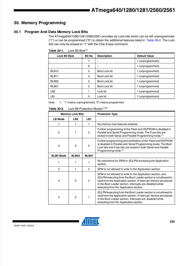
8/20/2019 At Mega 1281 Unlocked
http://slidepdf.com/reader/full/at-mega-1281-unlocked 335/446
335
2549P–AVR–10/2012
ATmega640/1280/1281/2560/2561
30. Memory Programming
30.1 Program And Data Memory Lock Bits
The ATmega640/1280/1281/2560/2561 provides six Lock bits which can be left unprogrammed
(“1”) or can be programmed (“0”) to obtain the additional features listed in Table 30-2. The Lock
bits can only be erased to “1” with the Chip Erase command.
Note: 1. “1” means unprogrammed, “0” means programmed
Table 30-1. Lock Bit Byte(1)
Lock Bit Byte Bit No Description Default Value
7 – 1 (unprogrammed)
6 – 1 (unprogrammed)
BLB12 5 Boot Lock bit 1 (unprogrammed)
BLB11 4 Boot Lock bit 1 (unprogrammed)
BLB02 3 Boot Lock bit 1 (unprogrammed)
BLB01 2 Boot Lock bit 1 (unprogrammed)
LB2 1 Lock bit 1 (unprogrammed)
LB1 0 Lock bit 1 (unprogrammed)
Table 30-2. Lock Bit Protection Modes(1)(2)
Memory Lock Bits Protection Type
LB Mode LB2 LB1
1 1 1 No memory lock features enabled.
2 1 0Further programming of the Flash and EEPROM is disabled inParallel and Serial Programming mode. The Fuse bits are
locked in both Serial and Parallel Programming mode.(1)
3 0 0
Further programming and verification of the Flash and EEPROMis disabled in Parallel and Serial Programming mode. The BootLock bits and Fuse bits are locked in both Serial and ParallelProgramming mode.(1)
BLB0 Mode BLB02 BLB01
1 1 1 No restrictions for SPM or (E)LPM accessing the Application
section.
2 1 0 SPM is not allowed to write to the Application section.
3 0 0
SPM is not allowed to write to the Application section, and(E)LPM executing from the Boot Loader section is not allowed to
read from the Application section. If Interrupt Vectors are placedin the Boot Loader section, interrupts are disabled whileexecuting from the Application section.
4 0 1
(E)LPM executing from the Boot Loader section is not allowed toread from the Application section. If Interrupt Vectors are placedin the Boot Loader section, interrupts are disabled whileexecuting from the Application section.

8/20/2019 At Mega 1281 Unlocked
http://slidepdf.com/reader/full/at-mega-1281-unlocked 336/446
336
2549P–AVR–10/2012
ATmega640/1280/1281/2560/2561
Notes: 1. Program the Fuse bits and Boot Lock bits before programming the LB1 and LB2.2. “1” means unprogrammed, “0” means programmed.
30.2 Fuse Bits
The ATmega640/1280/1281/2560/2561 has three Fuse bytes. Table 30-3 through Table 30-5 on
page 337 describe briefly the functionality of all the fuses and how they are mapped into the
Fuse bytes. Note that the fuses are read as logical zero, “0”, if they are programmed.
Note: 1. See “System and Reset Characteristics” on page 372 for BODLEVEL Fuse decoding.
BLB1 Mode BLB12 BLB11
1 1 1 No restrictions for SPM or (E)LPM accessing the Boot Loader
section.
2 1 0 SPM is not allowed to write to the Boot Loader section.
3 0 0
SPM is not allowed to write to the Boot Loader section, and(E)LPM executing from the Application section is not allowed toread from the Boot Loader section. If Interrupt Vectors areplaced in the Application section, interrupts are disabled whileexecuting from the Boot Loader section.
4 0 1
(E)LPM executing from the Application section is not allowed toread from the Boot Loader section. If Interrupt Vectors areplaced in the Application section, interrupts are disabled whileexecuting from the Boot Loader section.
Table 30-2. Lock Bit Protection Modes(1)(2) (Continued)
Memory Lock Bits Protection Type
Table 30-3. Extended Fuse Byte
Extended Fuse Byte Bit No Description Default Value
– 7 – 1
– 6 – 1
– 5 – 1
– 4 – 1
– 3 – 1
BODLEVEL2(1) 2 Brown-out Detector trigger level 1 (unprogrammed)
BODLEVEL1(1) 1 Brown-out Detector trigger level 1 (unprogrammed)
BODLEVEL0(1) 0 Brown-out Detector trigger level 1 (unprogrammed)

8/20/2019 At Mega 1281 Unlocked
http://slidepdf.com/reader/full/at-mega-1281-unlocked 337/446
337
2549P–AVR–10/2012
ATmega640/1280/1281/2560/2561
Notes: 1. The SPIEN Fuse is not accessible in serial programming mode.
2. The default value of BOOTSZ1:0 results in maximum Boot Size. See Table 29-7 on page 328 for details.
3. See “WDTCSR – Watchdog Timer Control Register” on page 67 for details.
4. Never ship a product with the OCDEN Fuse programmed regardless of the setting of Lock bitsand JTAGEN Fuse. A programmed OCDEN Fuse enables some parts of the clock system tobe running in all sleep modes. This may increase the power consumption.
Notes: 1. The default value of SUT1:0 results in maximum start-up time for the default clock source. See“System and Reset Characteristics” on page 372 for details.
2. The default setting of CKSEL3:0 results in internal RC Oscillator @ 8 MHz. See Table 10-1 onpage 41 for details.
3. The CKOUT Fuse allow the system clock to be output on PORTE7. See “Clock Output Buffer”on page 49 for details.
4. See “System Clock Prescaler” on page 49 for details.
The status of the Fuse bits is not affected by Chip Erase. Note that the Fuse bits are locked i
Lock bit1 (LB1) is programmed. Program the Fuse bits before programming the Lock bits.
Table 30-4. Fuse High Byte
Fuse High Byte Bit No Description Default Value
OCDEN(4) 7 Enable OCD
1 (unprogrammed, OCDdisabled)
JTAGEN 6 Enable JTAG 0 (programmed, JTAG enabled)
SPIEN(1) 5
Enable Serial Program and DataDownloading
0 (programmed, SPI prog.enabled)
WDTON(3) 4 Watchdog Timer always on 1 (unprogrammed)
EESAVE 3EEPROM memory is preservedthrough the Chip Erase
1 (unprogrammed, EEPROMnot preserved)
BOOTSZ1 2Select Boot Size (see Table 30-9 onpage 339 for details)
0 (programmed)(2)
BOOTSZ0 1Select Boot Size (see Table 30-9 onpage 339 for details)
0 (programmed)(2)
BOOTRST 0 Select Reset Vector 1 (unprogrammed)
Table 30-5. Fuse Low Byte
Fuse Low Byte Bit No Description Default Value
CKDIV8(4) 7 Divide clock by 8 0 (programmed)
CKOUT(3) 6 Clock output 1 (unprogrammed)
SUT1 5 Select start-up time 1 (unprogrammed)(1)
SUT0 4 Select start-up time 0 (programmed)(1)
CKSEL3 3 Select Clock source 0 (programmed)(2)
CKSEL2 2 Select Clock source 0 (programmed)(2)
CKSEL1 1 Select Clock source 1 (unprogrammed)(2)
CKSEL0 0 Select Clock source 0 (programmed)(2)

8/20/2019 At Mega 1281 Unlocked
http://slidepdf.com/reader/full/at-mega-1281-unlocked 338/446
338
2549P–AVR–10/2012
ATmega640/1280/1281/2560/2561
30.2.1 Latching of Fuses
The fuse values are latched when the device enters programming mode and changes of the
fuse values will have no effect until the part leaves Programming mode. This does not apply to
the EESAVE Fuse which will take effect once it is programmed. The fuses are also latched on
Power-up in Normal mode.
30.3 Signature BytesAll Atmel microcontrollers have a three-byte signature code which identifies the device. This
code can be read in both serial and parallel mode, also when the device is locked. The three
bytes reside in a separate address space. For the ATmega640/1280/1281/2560/2561 the signa
ture bytes are given in Table 30-6.
30.4 Calibration Byte
The ATmega640/1280/1281/2560/2561 has a byte calibration value for the internal RC Oscilla-
tor. This byte resides in the high byte of address 0x000 in the signature address space. During
reset, this byte is automatically written into the OSCCAL Register to ensure correct frequency o
the calibrated RC Oscillator.
30.5 Page Size
30.6 Parallel Programming Parameters, Pin Mapping, and Commands
This section describes how to parallel program and verify Flash Program memory, EEPROM
Data memory, Memory Lock bits, and Fuse bits in the ATmega640/1280/1281/2560/2561
Pulses are assumed to be at least 250ns unless otherwise noted.
Table 30-6. Device and JTAG ID
Part
Signature Bytes Address JTAG
0x000 0x001 0x002 Part Number Manufacture ID
ATmega640 0x1E 0x96 0x08 9608 0x1F
ATmega1280 0x1E 0x97 0x03 9703 0x1FATmega1281 0x1E 0x97 0x04 9704 0x1F
ATmega2560 0x1E 0x98 0x01 9801 0x1F
ATmega2561 0x1E 0x98 0x02 9802 0x1F
Table 30-7. No. of Words in a Page and No. of Pages in the Flash
Flash Size Page Size PCWORD
No. of
Pages PCPAGE PCMSB
128K words (256Kbytes) 128 words PC[6:0] 1024 PC[16:7] 16
Table 30-8. No. of Words in a Page and No. of Pages in the EEPROM
EEPROM Size Page Size PCWORD
No. of
Pages PCPAGE EEAMSB
4Kbytes 8 bytes EEA[2:0] 512 EEA[11:3] 11

8/20/2019 At Mega 1281 Unlocked
http://slidepdf.com/reader/full/at-mega-1281-unlocked 339/446
339
2549P–AVR–10/2012
ATmega640/1280/1281/2560/2561
30.6.1 Signal Names
In this section, some pins of the ATmega640/1280/1281/2560/2561 are referenced by signal
names describing their functionality during parallel programming, see Figure 30-1 and Table 30
9. Pins not described in the following table are referenced by pin names.
The XA1/XA0 pins determine the action executed when the XTAL1 pin is given a positive pulse
The bit coding is shown in Table 30-12 on page 340.When pulsing WR or OE, the command loaded determines the action executed. The differen
commands are shown in Table 30-13 on page 340.
Figure 30-1. Parallel Programming(1)
Note: 1. Unused Pins should be left floating.
Table 30-9. Pin Name MappingSignal Name in
Programming Mode Pin Name I/O Function
RDY/BSY PD1 O0: Device is busy programming, 1: Device is ready fornew command
OE PD2 I Output Enable (Active low)
WR PD3 I Write Pulse (Active low)
BS1 PD4 I Byte Select 1
XA0 PD5 I XTAL Action Bit 0
XA1 PD6 I XTAL Action Bit 1
PAGEL PD7 I Program Memory and EEPROM data Page Load
BS2 PA0 I Byte Select 2
DATA PB7-0 I/O Bi-directional Data bus (Output when OE is low)
VCC
+5V
GND
XTAL1
PD1
PD2
PD3
PD4
PD5
PD6
PB7 - PB0 DATA
RESET
PD7
+12V
BS1
XA0
XA1
OE
RDY/BSY
PAGEL
PA0
WR
BS2
AVCC
+5V

8/20/2019 At Mega 1281 Unlocked
http://slidepdf.com/reader/full/at-mega-1281-unlocked 340/446
340
2549P–AVR–10/2012
ATmega640/1280/1281/2560/2561
Table 30-10. BS2 and BS1 Encoding
BS2 BS1
Flash / EEPROM
Address
Flash Data
Loading /
Reading
Fuse
Programming
Reading Fuse
and Lock Bits
0 0 Low Byte Low Byte Low Byte Fuse Low Byte
0 1 High Byte High Byte High Byte Lockbits
1 0Extended High
ByteReserved Extended Byte
Extended FuseByte
1 1 Reserved Reserved Reserved Fuse High Byte
Table 30-11. Pin Values Used to Enter Programming Mode
Pin Symbol Value
PAGEL Prog_enable[3] 0
XA1 Prog_enable[2] 0
XA0 Prog_enable[1] 0
BS1 Prog_enable[0] 0
Table 30-12. XA1 and XA0 Enoding
XA1 XA0 Action when XTAL1 is Pulsed
0 0 Load Flash or EEPROM Address (High or low address byte determinedby BS2 and BS1)
0 1 Load Data (High or Low data byte for Flash determined by BS1)
1 0 Load Command
1 1 No Action, Idle
Table 30-13. Command Byte Bit Encoding
Command Byte Command Executed
1000 0000 Chip Erase
0100 0000 Write Fuse bits
0010 0000 Write Lock bits
0001 0000 Write Flash
0001 0001 Write EEPROM
0000 1000 Read Signature Bytes and Calibration byte
0000 0100 Read Fuse and Lock bits
0000 0010 Read Flash
0000 0011 Read EEPROM
8/20/2019 At Mega 1281 Unlocked
http://slidepdf.com/reader/full/at-mega-1281-unlocked 341/446
341
2549P–AVR–10/2012
ATmega640/1280/1281/2560/2561
30.7 Parallel Programming
30.7.1 Enter Programming Mode
The following algorithm puts the device in parallel programming mode:
1. Apply 4.5V - 5.5V between VCC and GND.
2. Set RESET to “0” and toggle XTAL1 at least six times.3. Set the Prog_enable pins listed in Table 30-11 on page 340 to “0000” and wait at least
100ns.
4. Apply 11.5V - 12.5V to RESET. Any activity on Prog_enable pins within 100ns after +12Vhas been applied to RESET, will cause the device to fail entering programming mode.
5. Wait at least 50µs before sending a new command.
30.7.2 Considerations for Efficient Programming
The loaded command and address are retained in the device during programming. For efficient
programming, the following should be considered.
• The command needs only be loaded once when writing or reading multiple memory
locations• Skip writing the data value 0xFF, that is the contents of the entire EEPROM (unless the
EESAVE Fuse is programmed) and Flash after a Chip Erase
• Address high byte needs only be loaded before programming or reading a new 256 wordwindow in Flash or 256 byte EEPROM. This consideration also applies to Signature bytesreading
30.7.3 Chip Erase
The Chip Erase will erase the Flash and EEPROM(1) memories plus Lock bits. The Lock bits are
not reset until the program memory has been completely erased. The Fuse bits are not
changed. A Chip Erase must be performed before the Flash and/or EEPROM are
reprogrammed.
Note: 1. The EEPRPOM memory is preserved during Chip Erase if the EESAVE Fuse is programmed
Load Command “Chip Erase”
1. Set XA1, XA0 to “10”. This enables command loading.
2. Set BS1 to “0”.
3. Set DATA to “1000 0000”. This is the command for Chip Erase.
4. Give XTAL1 a positive pulse. This loads the command.
5. Give WR a negative pulse. This starts the Chip Erase. RDY/BSY goes low.
6. Wait until RDY/BSY goes high before loading a new command.
30.7.4 Programming the Flash
The Flash is organized in pages, see Table 30-7 on page 338. When programming the Flashthe program data is latched into a page buffer. This allows one page of program data to be pro-
grammed simultaneously. The following procedure describes how to program the entire Flash
memory:
A. Load Command “Write Flash”
1. Set XA1, XA0 to “10”. This enables command loading.
2. Set BS1 to “0”.

8/20/2019 At Mega 1281 Unlocked
http://slidepdf.com/reader/full/at-mega-1281-unlocked 342/446
342
2549P–AVR–10/2012
ATmega640/1280/1281/2560/2561
3. Set DATA to “0001 0000”. This is the command for Write Flash.
4. Give XTAL1 a positive pulse. This loads the command.
B. Load Address Low byte (Address bits 7:0)
1. Set XA1, XA0 to “00”. This enables address loading.
2. Set BS2, BS1 to “00”. This selects the address low byte.
3. Set DATA = Address low byte (0x00 - 0xFF).4. Give XTAL1 a positive pulse. This loads the address low byte.
C. Load Data Low Byte
1. Set XA1, XA0 to “01”. This enables data loading.
2. Set DATA = Data low byte (0x00 - 0xFF).
3. Give XTAL1 a positive pulse. This loads the data byte.
D. Load Data High Byte
1. Set BS1 to “1”. This selects high data byte.
2. Set XA1, XA0 to “01”. This enables data loading.
3. Set DATA = Data high byte (0x00 - 0xFF).
4. Give XTAL1 a positive pulse. This loads the data byte.
E. Latch Data
1. Set BS1 to “1”. This selects high data byte.
2. Give PAGEL a positive pulse. This latches the data bytes. See Figure 30-3 on page 343for signal waveforms.
F. Repeat B through E until the entire buffer is filled or until all data within the page is loaded
While the lower bits in the address are mapped to words within the page, the higher bits address
the pages within the FLASH. This is illustrated in Figure 30-2 on page 343. Note that if less than
eight bits are required to address words in the page (pagesize < 256), the most significant bit(s
in the address low byte are used to address the page when performing a Page Write.
G. Load Address High byte (Address bits15:8)
1. Set XA1, XA0 to “00”. This enables address loading.
2. Set BS2, BS1 to “01”. This selects the address high byte.
3. Set DATA = Address high byte (0x00 - 0xFF).
4. Give XTAL1 a positive pulse. This loads the address high byte.
H. Load Address Extended High byte (Address bits 23:16)
1. Set XA1, XA0 to “00”. This enables address loading.
2. Set BS2, BS1 to “10”. This selects the address extended high byte.
3. Set DATA = Address extended high byte (0x00 - 0xFF).
4. Give XTAL1 a positive pulse. This loads the address high byte.I. Program Page
1. Set BS2, BS1 to “00”.
2. Give WR a negative pulse. This starts programming of the entire page of data. RDY/BSYgoes low.
3. Wait until RDY/BSY goes high (see Figure 30-3 on page 343 for signal waveforms).
J. Repeat B through I until the entire Flash is programmed or until all data has been
programmed

8/20/2019 At Mega 1281 Unlocked
http://slidepdf.com/reader/full/at-mega-1281-unlocked 343/446
343
2549P–AVR–10/2012
ATmega640/1280/1281/2560/2561
K. End Page Programming
1. 1. Set XA1, XA0 to “10”. This enables command loading.
2. Set DATA to “0000 0000”. This is the command for No Operation.
3. Give XTAL1 a positive pulse. This loads the command, and the internal write signals arereset.
Figure 30-2. Addressing the Flash Which is Organized in Pages(1)
Note: 1. PCPAGE and PCWORD are listed in Table 30-7 on page 338.
Figure 30-3. Programming the Flash Waveforms(1)
Note: 1. “XX” is don’t care. The letters refer to the programming description above.
30.7.5 Programming the EEPROM
The EEPROM is organized in pages, see Table 30-8 on page 338. When programming the
EEPROM, the program data is latched into a page buffer. This allows one page of data to be
programmed simultaneously. The programming algorithm for the EEPROM data memory is as
PROGRAM MEMORY
WORD ADDRESS
WITHIN A PAGE
PAGE ADDRESS
WITHIN THE FLASH
INSTRUCTION WORD
PAGE PCWORD[PAGEMSB:0]:
00
01
02
PAGEEND
PAGE
PCWORDPCPAGE
PCMSB PAGEMSBPROGRAM
COUNTER
RDY/BSY
WR
OE
RESE T + 12V
PAGEL
BS2
0x10 ADDR. LOW ADDR. HIGHDATA
DATA LOW DATA HIGH ADDR. LOW DATA LOW DATA HIGH
XA1
XA0
BS1
XTAL1
XX XX XX
A B C D E B C D E G
F
ADDR. EXT.H
H I

8/20/2019 At Mega 1281 Unlocked
http://slidepdf.com/reader/full/at-mega-1281-unlocked 344/446
344
2549P–AVR–10/2012
ATmega640/1280/1281/2560/2561
follows (refer to “Programming the Flash” on page 341 for details on Command, Address and
Data loading):
1. A: Load Command “0001 0001”.
2. G: Load Address High Byte (0x00 - 0xFF).
3. B: Load Address Low Byte (0x00 - 0xFF).
4. C: Load Data (0x00 - 0xFF).5. E: Latch data (give PAGEL a positive pulse).
K: Repeat 3 through 5 until the entire buffer is filled
L: Program EEPROM page
1. Set BS2, BS1 to “00”.
2. Give WR a negative pulse. This starts programming of the EEPROM page. RDY/BSYgoes low.
3. Wait until to RDY/BSY goes high before programming the next page (see Figure 30-4 forsignal waveforms).
Figure 30-4. Programming the EEPROM Waveforms
30.7.6 Reading the Flash
The algorithm for reading the Flash memory is as follows (refer to “Programming the Flash” on
page 341 for details on Command and Address loading):
1. A: Load Command “0000 0010”.
2. H: Load Address Extended Byte (0x00- 0xFF).
3. G: Load Address High Byte (0x00 - 0xFF).
4. B: Load Address Low Byte (0x00 - 0xFF).
5. Set OE to “0”, and BS1 to “0”. The Flash word low byte can now be read at DATA.
6. Set BS to “1”. The Flash word high byte can now be read at DATA.
7. Set OE to “1”.
RDY/BSY
WR
OE
RESE T + 12 V
PAGEL
BS2
0x11 ADDR. HIGHDATA
ADDR. LOW DATA ADDR. LOW DATA XX
XA1
XA0
BS1
XTAL1
XX
A G B C E B C E L
K

8/20/2019 At Mega 1281 Unlocked
http://slidepdf.com/reader/full/at-mega-1281-unlocked 345/446
345
2549P–AVR–10/2012
ATmega640/1280/1281/2560/2561
30.7.7 Reading the EEPROM
The algorithm for reading the EEPROM memory is as follows (refer to “Programming the Flash
on page 341 for details on Command and Address loading):
1. A: Load Command “0000 0011”.
2. G: Load Address High Byte (0x00 - 0xFF).
3. B: Load Address Low Byte (0x00 - 0xFF).4. Set OE to “0”, and BS1 to “0”. The EEPROM Data byte can now be read at DATA.
5. Set OE to “1”.
30.7.8 Programming the Fuse Low Bits
The algorithm for programming the Fuse Low bits is as follows (refer to “Programming the Flash”
on page 341 for details on Command and Data loading):
1. A: Load Command “0100 0000”.
2. C: Load Data Low Byte. Bit n = “0” programs and bit n = “1” erases the Fuse bit.
3. Give WR a negative pulse and wait for RDY/BSY to go high.
30.7.9 Programming the Fuse High BitsThe algorithm for programming the Fuse High bits is as follows (refer to “Programming the
Flash” on page 341 for details on Command and Data loading):
1. A: Load Command “0100 0000”.
2. C: Load Data Low Byte. Bit n = “0” programs and bit n = “1” erases the Fuse bit.
3. Set BS2, BS1 to “01”. This selects high data byte.
4. Give WR a negative pulse and wait for RDY/BSY to go high.
5. Set BS2, BS1 to “00”. This selects low data byte.
30.7.10 Programming the Extended Fuse Bits
The algorithm for programming the Extended Fuse bits is as follows (refer to “Programming the
Flash” on page 341 for details on Command and Data loading):
1. 1. A: Load Command “0100 0000”.
2. 2. C: Load Data Low Byte. Bit n = “0” programs and bit n = “1” erases the Fuse bit.
3. 3. Set BS2, BS1 to “10”. This selects extended data byte.
4. 4. Give WR a negative pulse and wait for RDY/BSY to go high.
5. 5. Set BS2, BS1 to “00”. This selects low data byte.
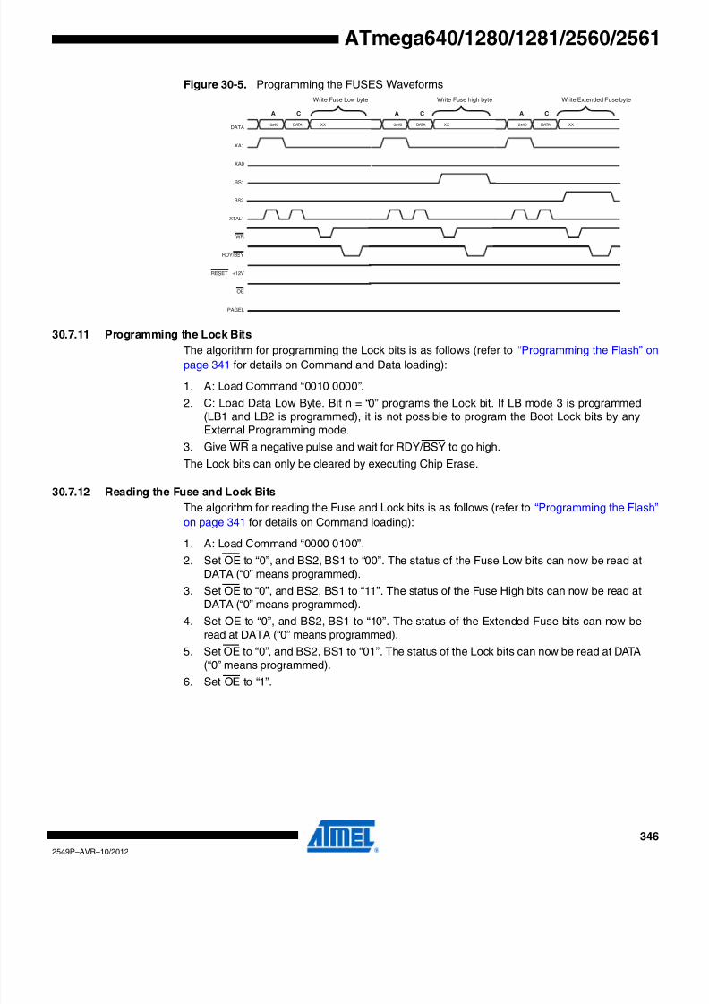
8/20/2019 At Mega 1281 Unlocked
http://slidepdf.com/reader/full/at-mega-1281-unlocked 346/446
346
2549P–AVR–10/2012
ATmega640/1280/1281/2560/2561
Figure 30-5. Programming the FUSES Waveforms
30.7.11 Programming the Lock Bits
The algorithm for programming the Lock bits is as follows (refer to “Programming the Flash” on
page 341 for details on Command and Data loading):
1. A: Load Command “0010 0000”.
2. C: Load Data Low Byte. Bit n = “0” programs the Lock bit. If LB mode 3 is programmed(LB1 and LB2 is programmed), it is not possible to program the Boot Lock bits by anyExternal Programming mode.
3. Give WR a negative pulse and wait for RDY/BSY to go high.
The Lock bits can only be cleared by executing Chip Erase.
30.7.12 Reading the Fuse and Lock Bits
The algorithm for reading the Fuse and Lock bits is as follows (refer to “Programming the Flash
on page 341 for details on Command loading):
1. A: Load Command “0000 0100”.
2. Set OE to “0”, and BS2, BS1 to “00”. The status of the Fuse Low bits can now be read atDATA (“0” means programmed).
3. Set OE to “0”, and BS2, BS1 to “11”. The status of the Fuse High bits can now be read atDATA (“0” means programmed).
4. Set OE to “0”, and BS2, BS1 to “10”. The status of the Extended Fuse bits can now beread at DATA (“0” means programmed).
5. Set OE to “0”, and BS2, BS1 to “01”. The status of the Lock bits can now be read at DATA(“0” means programmed).
6. Set OE to “1”.
RDY/BSY
WR
OE
RESET +12V
PAGEL
0x40DATA
DATA XX
XA1
XA0
BS1
XTAL1
A C
0x40 DATA XX
A C
Write Fuse Low byte Write Fuse high byte
0x40 DATA XX
A C
Write Extended Fuse byte
BS2

8/20/2019 At Mega 1281 Unlocked
http://slidepdf.com/reader/full/at-mega-1281-unlocked 347/446
347
2549P–AVR–10/2012
ATmega640/1280/1281/2560/2561
Figure 30-6. Mapping Between BS1, BS2 and the Fuse and Lock Bits During Read
30.7.13 Reading the Signature Bytes
The algorithm for reading the Signature bytes is as follows (refer to “Programming the Flash” on
page 341 for details on Command and Address loading):
1. A: Load Command “0000 1000”.
2. B: Load Address Low Byte (0x00 - 0x02).
3. Set OE to “0”, and BS to “0”. The selected Signature byte can now be read at DATA.
4. Set OE to “1”.
30.7.14 Reading the Calibration Byte
The algorithm for reading the Calibration byte is as follows (refer to “Programming the Flash” on
page 341 for details on Command and Address loading):
1. A: Load Command “0000 1000”.
2. B: Load Address Low Byte, 0x00.3. Set OE to “0”, and BS1 to “1”. The Calibration byte can now be read at DATA.
4. Set OE to “1”.
30.7.15 Parallel Programming Characteristics
Figure 30-7. Parallel Programming Timing, Including some General Timing Requirements
Lock Bits 0
1
BS2
Fuse High Byte
0
1
BS1
DATA
Fuse Low Byte 0
1
BS2
Extended Fuse Byte
Data & Contol(DATA, XA0/1, BS1, BS2)
XTAL1 tXHXL
tWLWH
tDVXH tXLDX
tPLWL
tWLRH
WR
RDY/BSY
PAGEL tPHPL
tPLBXtBVPH
tXLWL
tWLBXtBVWL
WLRL
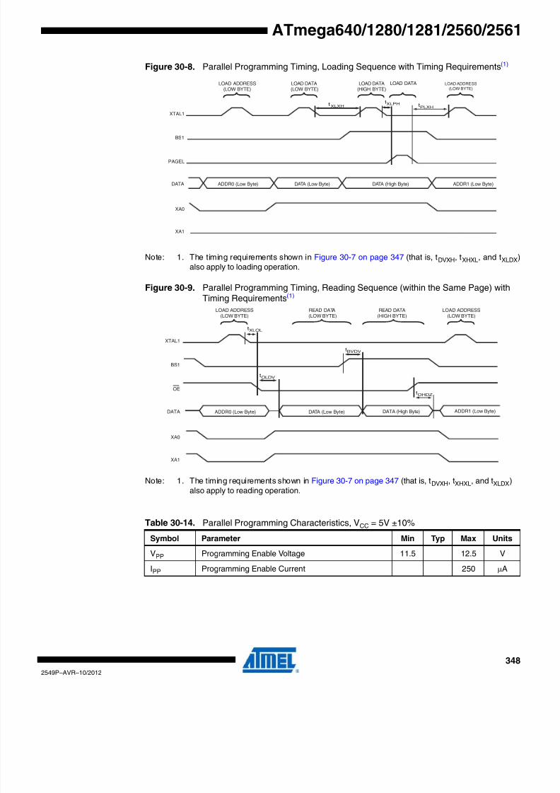
8/20/2019 At Mega 1281 Unlocked
http://slidepdf.com/reader/full/at-mega-1281-unlocked 348/446
348
2549P–AVR–10/2012
ATmega640/1280/1281/2560/2561
Figure 30-8. Parallel Programming Timing, Loading Sequence with Timing Requirements(1)
Note: 1. The timing requirements shown in Figure 30-7 on page 347 (that is, tDVXH, tXHXL, and tXLDX
also apply to loading operation.
Figure 30-9. Parallel Programming Timing, Reading Sequence (within the Same Page) withTiming Requirements(1)
Note: 1. The timing requirements shown in Figure 30-7 on page 347 (that is, tDVXH, tXHXL, and tXLDX)also apply to reading operation.
Table 30-14. Parallel Programming Characteristics, VCC = 5V ±10%
Symbol Parameter Min Typ Max UnitsVPP Programming Enable Voltage 11.5 12.5 V
IPP Programming Enable Current 250 μA
XTAL1
PAGEL
tPLXHXLXH
t t
XLPH
ADDR0 (Low Byte) DATA (Low Byte) DATA (High Byte) ADDR1 (Low Byte)DATA
BS1
XA0
XA1
LOAD ADDRESS
(LOW BYTE)LOAD DATA(LOW BYTE)
LOAD DATA(HIGH BYTE)
LOAD DATA LOAD ADDRESS
(LOW BYTE)
XTAL1
OE
ADDR0 (Low Byte) DATA (Low Byte) DATA (High Byte) ADDR1 (Low Byte)DATA
BS1
XA0
XA1
LOAD ADDRESS(LOW BYTE)
READ DATA(LOW BYTE)
READ DATA(HIGH BYTE)
LOAD ADDRESS(LOW BYTE)
tBVDV
tOLDV
tXLOL
tOHDZ

8/20/2019 At Mega 1281 Unlocked
http://slidepdf.com/reader/full/at-mega-1281-unlocked 349/446
349
2549P–AVR–10/2012
ATmega640/1280/1281/2560/2561
Notes: 1. tWLRH is valid for the Write Flash, Write EEPROM, Write Fuse bits and Write Lock bits
commands.
2. tWLRH_CE is valid for the Chip Erase command.
30.8 Serial Downloading
Both the Flash and EEPROM memory arrays can be programmed using a serial programming
bus while RESET is pulled to GND. The serial programming interface consists of pins SCK, PD
(input) and PDO (output). After RESET is set low, the Programming Enable instruction needs to
be executed first before program/erase operations can be executed. NOTE, in Table 30-15 on
page 350, the pin mapping for serial programming is listed. Not all packages use the SPI pins
dedicated for the internal Serial Peripheral Interface - SPI.
tDVXH Data and Control Valid before XTAL1 High 67
ns
tXLXH XTAL1 Low to XTAL1 High 200
tXHXL XTAL1 Pulse Width High 150
tXLDX Data and Control Hold after XTAL1 Low 67
tXLWL XTAL1 Low to WR Low 0
tXLPH XTAL1 Low to PAGEL high 0
tPLXH PAGEL low to XTAL1 high 150
tBVPH BS1 Valid before PAGEL High 67
tPHPL PAGEL Pulse Width High 150
tPLBX BS1 Hold after PAGEL Low 67
tWLBX BS2/1 Hold after WR Low 67
tPLWL PAGEL Low to WR Low 67
tBVWL BS2/1 Valid to WR Low 67
tWLWH WR Pulse Width Low 150
tWLRL WR Low to RDY/BSY Low 0 1 μs
tWLRH WR Low to RDY/BSY High(1) 3.7 4.5ms
tWLRH_CE WR Low to RDY/BSY High for Chip Erase(2) 7.5 9
tXLOL XTAL1 Low to OE Low 0
nstBVDV BS1 Valid to DATA valid 0 250
tOLDV OE Low to DATA Valid 250
tOHDZ OE High to DATA Tri-stated 250
Table 30-14. Parallel Programming Characteristics, VCC = 5V ±10% (Continued)
Symbol Parameter Min Typ Max Units
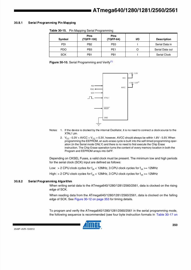
8/20/2019 At Mega 1281 Unlocked
http://slidepdf.com/reader/full/at-mega-1281-unlocked 350/446
350
2549P–AVR–10/2012
ATmega640/1280/1281/2560/2561
30.8.1 Serial Programming Pin Mapping
Figure 30-10. Serial Programming and Verify(1)
Notes: 1. If the device is clocked by the internal Oscillator, it is no need to connect a clock source to theXTAL1 pin.
2. VCC - 0.3V < AVCC < VCC + 0.3V, however, AVCC should always be within 1.8V - 5.5V.Whenprogramming the EEPROM, an auto-erase cycle is built into the self-timed programming oper-ation (in the Serial mode ONLY) and there is no need to first execute the Chip Eraseinstruction. The Chip Erase operation turns the content of every memory location in both theProgram and EEPROM arrays into 0xFF.
Depending on CKSEL Fuses, a valid clock must be present. The minimum low and high periods
for the serial clock (SCK) input are defined as follows:
Low: > 2 CPU clock cycles for fck < 12MHz, 3 CPU clock cycles for fck >= 12MHz
High: > 2 CPU clock cycles for fck < 12MHz, 3 CPU clock cycles for fck >= 12MHz
30.8.2 Serial Programming Algorithm
When writing serial data to the ATmega640/1280/1281/2560/2561, data is clocked on the risingedge of SCK.
When reading data from the ATmega640/1280/1281/2560/2561, data is clocked on the falling
edge of SCK. See Figure 30-12 on page 353 for timing details.
To program and verify the ATmega640/1280/1281/2560/2561 in the serial programming mode
the following sequence is recommended (see four byte instruction formats in Table 30-17 on
Table 30-15. Pin Mapping Serial Programming
Symbol
Pins
(TQFP-100)
Pins
(TQFP-64) I/O Description
PDI PB2 PE0 I Serial Data in
PDO PB3 PE1 O Serial Data out
SCK PB1 PB1 I Serial Clock
VCC
GND
XTAL1
SCK
PDO
PDI
RESET
+1.8V - 5.5V
AVCC
+1.8V - 5.5V(2)
8/20/2019 At Mega 1281 Unlocked
http://slidepdf.com/reader/full/at-mega-1281-unlocked 351/446
351
2549P–AVR–10/2012
ATmega640/1280/1281/2560/2561
page 352):
1. Power-up sequence:Apply power between VCC and GND while RESET and SCK are set to “0”. In some sys-tems, the programmer can not guarantee that SCK is held low during power-up. In thiscase, RESET must be given a positive pulse of at least two CPU clock cycles durationafter SCK has been set to “0”.
2. Wait for at least 20ms and enable serial programming by sending the ProgrammingEnable serial instruction to pin PDI.
3. The serial programming instructions will not work if the communication is out of synchro-nization. When in sync. the second byte (0x53), will echo back when issuing the thirdbyte of the Programming Enable instruction. Whether the echo is correct or not, all fourbytes of the instruction must be transmitted. If the 0x53 did not echo back, give RESET apositive pulse and issue a new Programming Enable command.
4. The Flash is programmed one page at a time. The memory page is loaded one byte at atime by supplying the 7 LSB of the address and data together with the Load ProgramMemory Page instruction. To ensure correct loading of the page, the data low byte mustbe loaded before data high byte is applied for a given address. The Program MemoryPage is stored by loading the Write Program Memory Page instruction with the address
lines 15:8. Before issuing this command, make sure the instruction Load ExtendedAddress Byte has been used to define the MSB of the address. The extended addressbyte is stored until the command is re-issued, that is, the command needs only be issuedfor the first page, and when crossing the 64KWord boundary. If polling (RDY/BSY) is notused, the user must wait at least tWD_FLASH before issuing the next page (see Table 30-16). Accessing the serial programming interface before the Flash write operation com-pletes can result in incorrect programming.
5. The EEPROM array is programmed one byte at a time by supplying the address and datatogether with the appropriate Write instruction. An EEPROM memory location is firstautomatically erased before new data is written. If polling is not used, the user must waitat least tWD_EEPROM before issuing the next byte (see Table 30-16). In a chip eraseddevice, no 0xFFs in the data file(s) need to be programmed.
6. Any memory location can be verified by using the Read instruction which returns the con-tent at the selected address at serial output PDO. When reading the Flash memory, usethe instruction Load Extended Address Byte to define the upper address byte, which isnot included in the Read Program Memory instruction. The extended address byte isstored until the command is re-issued, that is, the command needs only be issued for thefirst page, and when crossing the 64KWord boundary.
7. At the end of the programming session, RESET can be set high to commence normaloperation.
8. Power-off sequence (if needed):Set RESET to “1”.Turn VCC power off.
Table 30-16. Minimum Wait Delay Before Writing the Next Flash or EEPROM Location
Symbol Minimum Wait Delay
tWD_FLASH 4.5ms
tWD_EEPROM 3.6ms
tWD_ERASE 9.0ms

8/20/2019 At Mega 1281 Unlocked
http://slidepdf.com/reader/full/at-mega-1281-unlocked 352/446
352
2549P–AVR–10/2012
ATmega640/1280/1281/2560/2561
30.8.3 Serial Programming Instruction set
Table 30-17 and Figure 30-11 on page 353 describes the Instruction set.
Notes: 1. Not all instructions are applicable for all parts.
2. a = address.
3. Bits are programmed ‘0’, unprogrammed ‘1’.
4. To ensure future compatibility, unused Fuses and Lock bits should be unprogrammed (‘1’).
5. Refer to the correspondig section for Fuse and Lock bits, Calibration and Signature bytes andPage size.
6. See htt://www.atmel.com/avr for Application Notes regarding programming and programmers.
If the LSB in RDY/BSY data byte out is ‘1’, a programming operation is still pending. Wait unti
this bit returns ‘0’ before the next instruction is carried out.
Table 30-17. Serial Programming Instruction Set
Instruction/Operation
Instruction Format
Byte 1 Byte 2 Byte 3 Byte 4
Programming Enable $AC $53 $00 $00
Chip Erase (Program Memory/EEPROM) $AC $80 $00 $00
Poll RDY/BSY $F0 $00 $00 data byte out
Load Instructions
Load Extended Address byte(1) $4D $00 Extended adr $00
Load Program Memory Page, High byte $48 $00 adr LSB high data byte in
Load Program Memory Page, Low byte $40 $00 adr LSB low data byte in
Load EEPROM Memory Page (page access) $C1 $00 0000 000aa data byte in
Read Instructions
Read Program Memory, High byte $28 adr MSB adr LSB high data byte out
Read Program Memory, Low byte $20 adr MSB adr LSB low data byte out
Read EEPROM Memory $A0 0000 aaaa aaaa aaaa data byte out
Read Lock bits $58 $00 $00 data byte out
Read Signature Byte $30 $00 0000 000aa data byte out
Read Fuse bits $50 $00 $00 data byte out
Read Fuse High bits $58 $08 $00 data byte out
Read Extended Fuse Bits $50 $08 $00 data byte out
Read Calibration Byte $38 $00 $00 data byte out
Write Instructions
Write Program Memory Page $4C adr MSB adr LSB $00
Write EEPROM Memory $C0 0000 aaaa aaaa aaaa data byte in
Write EEPROM Memory Page (page access) $C2 0000 aaaa aaaa 00 $00
Write Lock bits $AC $E0 $00 data byte in
Write Fuse bits $AC $A0 $00 data byte in
Write Fuse High bits $AC $A8 $00 data byte in
Write Extended Fuse Bits $AC $A4 $00 data byte in

8/20/2019 At Mega 1281 Unlocked
http://slidepdf.com/reader/full/at-mega-1281-unlocked 353/446
353
2549P–AVR–10/2012
ATmega640/1280/1281/2560/2561
Within the same page, the low data byte must be loaded prior to the high data byte.
After data is loaded to the page buffer, program the EEPROM page, see Figure 30-11.
Figure 30-11. Serial Programming Instruction example
30.8.4 Serial Programming Characteristics
For characteristics of the Serial Programming module, see “SPI Timing Characteristics” on page
375.
Figure 30-12. Serial Programming Waveforms
Byte 1 Byte 2 Byte 3 Byte 4
Adr LSB
Bit 15 B 0
Serial Programming Instruction
Program Memory/ EEPROM Memory
Page 0
Page 1
Page 2
Page N-1
Page Buffer
Write Program Memory Page/
Write EEPROM Memory Page
Load Program Memory Page (High/Low Byte)/
Load EEPROM Memory Page (page access)
Byte 1 Byte 2 Byte 3 Byte 4
Bit 15 B 0
Adr MSB
Page Offset
Page Number
MSB
MSB
LSB
LSB
SERIAL CLOCK INPUT(SCK)
SERIAL DATA INPUT (MOSI)
(MISO)
SAMPLE
SERIAL DATA OUTPUT

8/20/2019 At Mega 1281 Unlocked
http://slidepdf.com/reader/full/at-mega-1281-unlocked 354/446
354
2549P–AVR–10/2012
ATmega640/1280/1281/2560/2561
30.9 Programming via the JTAG Interface
Programming through the JTAG interface requires control of the four JTAG specific pins: TCK
TMS, TDI, and TDO. Control of the reset and clock pins is not required.
To be able to use the JTAG interface, the JTAGEN Fuse must be programmed. The device isdefault shipped with the fuse programmed. In addition, the JTD bit in MCUCR must be cleared.
Alternatively, if the JTD bit is set, the external reset can be forced low. Then, the JTD bit will be
cleared after two chip clocks, and the JTAG pins are available for programming. This provides a
means of using the JTAG pins as normal port pins in Running mode while still allowing In-Sys-
tem Programming via the JTAG interface. Note that this technique can not be used when using
the JTAG pins for Boundary-scan or On-chip Debug. In these cases the JTAG pins must be ded
icated for this purpose.
During programming the clock frequency of the TCK Input must be less than the maximum fre-
quency of the chip. The System Clock Prescaler can not be used to divide the TCK Clock Input
into a sufficiently low frequency.
As a definition in this datasheet, the LSB is shifted in and out first of all Shift Registers.
30.9.1 Programming Specific JTAG Instructions
The Instruction Register is 4-bit wide, supporting up to 16 instructions. The JTAG instructions
useful for programming are listed below.
The OPCODE for each instruction is shown behind the instruction name in hex format. The text
describes which Data Register is selected as path between TDI and TDO for each instruction.
The Run-Test/Idle state of the TAP controller is used to generate internal clocks. It can also be
used as an idle state between JTAG sequences. The state machine sequence for changing the
instruction word is shown in Figure 30-13 on page 355.
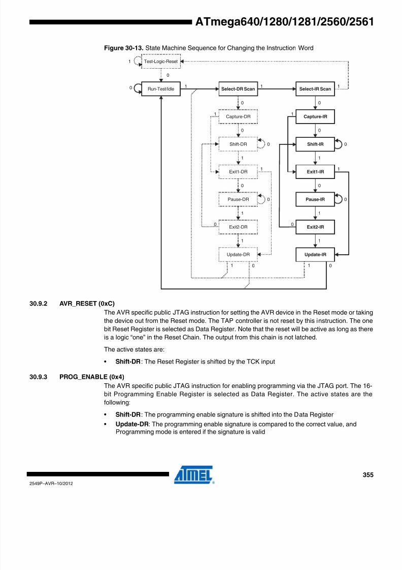
8/20/2019 At Mega 1281 Unlocked
http://slidepdf.com/reader/full/at-mega-1281-unlocked 355/446
355
2549P–AVR–10/2012
ATmega640/1280/1281/2560/2561
Figure 30-13. State Machine Sequence for Changing the Instruction Word
30.9.2 AVR_RESET (0xC)
The AVR specific public JTAG instruction for setting the AVR device in the Reset mode or taking
the device out from the Reset mode. The TAP controller is not reset by this instruction. The one
bit Reset Register is selected as Data Register. Note that the reset will be active as long as there
is a logic “one” in the Reset Chain. The output from this chain is not latched.
The active states are:
• Shift-DR: The Reset Register is shifted by the TCK input
30.9.3 PROG_ENABLE (0x4)
The AVR specific public JTAG instruction for enabling programming via the JTAG port. The 16-
bit Programming Enable Register is selected as Data Register. The active states are the
following:
• Shift-DR: The programming enable signature is shifted into the Data Register
• Update-DR: The programming enable signature is compared to the correct value, andProgramming mode is entered if the signature is valid
Test-Logic-Reset
Run-Test/Idle
Shift-DR
Exit1-DR
Pause-DR
Exit2-DR
Update-DR
Select-IR Scan
Capture-IR
Shift-IR
Exit1-IR
Pause-IR
Exit2-IR
Update-IR
Select-DR Scan
Capture-DR
0
1
0 1 1 1
0 0
0 0
1 1
1 0
1
1
0
1
0
0
1 0
1
1
0
1
0
0
00
11

8/20/2019 At Mega 1281 Unlocked
http://slidepdf.com/reader/full/at-mega-1281-unlocked 356/446
356
2549P–AVR–10/2012
ATmega640/1280/1281/2560/2561
30.9.4 PROG_COMMANDS (0x5)
The AVR specific public JTAG instruction for entering programming commands via the JTAG
port. The 15-bit Programming Command Register is selected as Data Register. The active
states are the following:
• Capture-DR: The result of the previous command is loaded into the Data Register
• Shift-DR: The Data Register is shifted by the TCK input, shifting out the result of theprevious command and shifting in the new command
• Update-DR: The programming command is applied to the Flash inputs
• Run-Test/Idle: One clock cycle is generated, executing the applied command
30.9.5 PROG_PAGELOAD (0x6)
The AVR specific public JTAG instruction to directly load the Flash data page via the JTAG port
An 8-bit Flash Data Byte Register is selected as the Data Register. This is physically the 8 LSBs
of the Programming Command Register. The active states are the following:
• Shift-DR: The Flash Data Byte Register is shifted by the TCK input.
• Update-DR: The content of the Flash Data Byte Register is copied into a temporary register.
A write sequence is initiated that within 11 TCK cycles loads the content of the temporaryregister into the Flash page buffer. The AVR automatically alternates between writing the lowand the high byte for each new Update-DR state, starting with the low byte for the firstUpdate-DR encountered after entering the PROG_PAGELOAD command. The ProgramCounter is pre-incremented before writing the low byte, except for the first written byte. Thisensures that the first data is written to the address set up by PROG_COMMANDS, andloading the last location in the page buffer does not make the program counter incrementinto the next page.
30.9.6 PROG_PAGEREAD (0x7)
The AVR specific public JTAG instruction to directly capture the Flash content via the JTAG port
An 8-bit Flash Data Byte Register is selected as the Data Register. This is physically the 8 LSBs
of the Programming Command Register. The active states are the following:
• Capture-DR: The content of the selected Flash byte is captured into the Flash Data ByteRegister. The AVR automatically alternates between reading the low and the high byte foreach new Capture-DR state, starting with the low byte for the first Capture-DR encounteredafter entering the PROG_PAGEREAD command. The Program Counter is post-incrementedafter reading each high byte, including the first read byte. This ensures that the first data iscaptured from the first address set up by PROG_COMMANDS, and reading the last locationin the page makes the program counter increment into the next page.
• Shift-DR: The Flash Data Byte Register is shifted by the TCK input.
30.9.7 Data Registers
The Data Registers are selected by the JTAG instruction registers described in section “Pro
gramming Specific JTAG Instructions” on page 354. The Data Registers relevant forprogramming operations are:
• Reset Register
• Programming Enable Register
• Programming Command Register
• Flash Data Byte Register

8/20/2019 At Mega 1281 Unlocked
http://slidepdf.com/reader/full/at-mega-1281-unlocked 357/446
357
2549P–AVR–10/2012
ATmega640/1280/1281/2560/2561
30.9.8 Reset Register
The Reset Register is a Test Data Register used to reset the part during programming. It is
required to reset the part before entering Programming mode.
A high value in the Reset Register corresponds to pulling the external reset low. The part is rese
as long as there is a high value present in the Reset Register. Depending on the Fuse settings
for the clock options, the part will remain reset for a Reset Time-out period (refer to “ClockSources” on page 41) after releasing the Reset Register. The output from this Data Register is
not latched, so the reset will take place immediately, as shown in Figure 28-2 on page 304.
30.9.9 Programming Enable Register
The Programming Enable Register is a 16-bit register. The contents of this register is compared
to the programming enable signature, binary code 0b1010_0011_0111_0000. When the con
tents of the register is equal to the programming enable signature, programming via the JTAG
port is enabled. The register is reset to 0 on Power-on Reset, and should always be reset when
leaving Programming mode.
Figure 30-14. Programming Enable Register
30.9.10 Programming Command Register
The Programming Command Register is a 15-bit register. This register is used to serially shift in
programming commands, and to serially shift out the result of the previous command, if any. The
JTAG Programming Instruction Set is shown in Table 30-18 on page 359. The state sequence
when shifting in the programming commands is i llustrated in Figure 30-16 on page 362.
TDI
TDO
D
A
T
A
= D Q
ClockDR & PROG_ENABLE
Programming Enable
0xA370

8/20/2019 At Mega 1281 Unlocked
http://slidepdf.com/reader/full/at-mega-1281-unlocked 358/446
358
2549P–AVR–10/2012
ATmega640/1280/1281/2560/2561
Figure 30-15. Programming Command Register
TDI
TDO
S
T
R
O
B
E
S
A
D
D
R
E
S
S
/
D
A
T
A
FlashEEPROM
FusesLock Bits

8/20/2019 At Mega 1281 Unlocked
http://slidepdf.com/reader/full/at-mega-1281-unlocked 359/446
359
2549P–AVR–10/2012
ATmega640/1280/1281/2560/2561
Table 30-18. JTAG Programming InstructionSet a = address high bits, b = address low bits, c = address extended bits, H = 0 - Low byte, 1 - High Byte, o = data out,
i = data in, x = don’t care
Instruction TDI Sequence TDO Sequence Notes
1a. Chip Erase0100011_100000000110001_10000000
0110011_10000000
0110011_10000000
xxxxxxx_xxxxxxxxxxxxxxx_xxxxxxxx
xxxxxxx_xxxxxxxx
xxxxxxx_xxxxxxxx
1b. Poll for Chip Erase Complete 0110011_10000000 xxxxxox_xxxxxxxx (2)
2a. Enter Flash Write 0100011_00010000 xxxxxxx_xxxxxxxx
2b. Load Address Extended High Byte 0001011_cccccccc xxxxxxx_xxxxxxxx (10)
2c. Load Address High Byte 0000111_aaaaaaaa xxxxxxx_xxxxxxxx
2d. Load Address Low Byte 0000011_bbbbbbbb xxxxxxx_xxxxxxxx
2e. Load Data Low Byte 0010011_iiiiiiii xxxxxxx_xxxxxxxx
2f. Load Data High Byte 0010111_iiiiiiii xxxxxxx_xxxxxxxx
2g. Latch Data
0110111_00000000
1110111_00000000
0110111_00000000
xxxxxxx_xxxxxxxx
xxxxxxx_xxxxxxxx
xxxxxxx_xxxxxxxx
(1)
2h. Write Flash Page
0110111_00000000
0110101_00000000
0110111_00000000
0110111_00000000
xxxxxxx_xxxxxxxx
xxxxxxx_xxxxxxxx
xxxxxxx_xxxxxxxx
xxxxxxx_xxxxxxxx
(1)
2i. Poll for Page Write Complete 0110111_00000000 xxxxxox_xxxxxxxx (2)
3a. Enter Flash Read 0100011_00000010 xxxxxxx_xxxxxxxx
3b. Load Address Extended High Byte 0001011_cccccccc xxxxxxx_xxxxxxxx (10)3c. Load Address High Byte 0000111_aaaaaaaa xxxxxxx_xxxxxxxx
3d. Load Address Low Byte 0000011_bbbbbbbb xxxxxxx_xxxxxxxx
3e. Read Data Low and High Byte
0110010_00000000
0110110_00000000
0110111_00000000
xxxxxxx_xxxxxxxx
xxxxxxx_oooooooo
xxxxxxx_oooooooo
Low byte
High byte
4a. Enter EEPROM Write 0100011_00010001 xxxxxxx_xxxxxxxx
4b. Load Address High Byte 0000111_aaaaaaaa xxxxxxx_xxxxxxxx (10)
4c. Load Address Low Byte 0000011_bbbbbbbb xxxxxxx_xxxxxxxx
4d. Load Data Byte 0010011_iiiiiiii xxxxxxx_xxxxxxxx
4e. Latch Data
0110111_00000000
1110111_00000000
0110111_00000000
xxxxxxx_xxxxxxxx
xxxxxxx_xxxxxxxx
xxxxxxx_xxxxxxxx
(1)
4f. Write EEPROM Page
0110011_00000000
0110001_00000000
0110011_00000000
0110011_00000000
xxxxxxx_xxxxxxxx
xxxxxxx_xxxxxxxx
xxxxxxx_xxxxxxxx
xxxxxxx_xxxxxxxx
(1)

8/20/2019 At Mega 1281 Unlocked
http://slidepdf.com/reader/full/at-mega-1281-unlocked 360/446
360
2549P–AVR–10/2012
ATmega640/1280/1281/2560/2561
4g. Poll for Page Write Complete 0110011_00000000 xxxxxox_xxxxxxxx (2)
5a. Enter EEPROM Read 0100011_00000011 xxxxxxx_xxxxxxxx5b. Load Address High Byte 0000111_aaaaaaaa xxxxxxx_xxxxxxxx (10)
5c. Load Address Low Byte 0000011_bbbbbbbb xxxxxxx_xxxxxxxx
5d. Read Data Byte
0110011_bbbbbbbb
0110010_00000000
0110011_00000000
xxxxxxx_xxxxxxxx
xxxxxxx_xxxxxxxx
xxxxxxx_oooooooo
6a. Enter Fuse Write 0100011_01000000 xxxxxxx_xxxxxxxx
6b. Load Data Low Byte(6) 0010011_iiiiiiii xxxxxxx_xxxxxxxx (3)
6c. Write Fuse Extended Byte
0111011_00000000
0111001_00000000
0111011_000000000111011_00000000
xxxxxxx_xxxxxxxx
xxxxxxx_xxxxxxxx
xxxxxxx_xxxxxxxxxxxxxxx_xxxxxxxx
(1)
6d. Poll for Fuse Write Complete 0110111_00000000 xxxxxox_xxxxxxxx (2)
6e. Load Data Low Byte(7) 0010011_iiiiiiii xxxxxxx_xxxxxxxx (3)
6f. Write Fuse High Byte
0110111_00000000
0110101_00000000
0110111_00000000
0110111_00000000
xxxxxxx_xxxxxxxx
xxxxxxx_xxxxxxxx
xxxxxxx_xxxxxxxx
xxxxxxx_xxxxxxxx
(1)
6g. Poll for Fuse Write Complete 0110111_00000000 xxxxxox_xxxxxxxx (2)
6h. Load Data Low Byte(7) 0010011_iiiiiiii xxxxxxx_xxxxxxxx (3)
6i. Write Fuse Low Byte
0110011_000000000110001_00000000
0110011_00000000
0110011_00000000
xxxxxxx_xxxxxxxxxxxxxxx_xxxxxxxx
xxxxxxx_xxxxxxxx
xxxxxxx_xxxxxxxx
(1)
6j. Poll for Fuse Write Complete 0110011_00000000 xxxxxox_xxxxxxxx (2)
7a. Enter Lock Bit Write 0100011_00100000 xxxxxxx_xxxxxxxx
7b. Load Data Byte(9) 0010011_11iiiiii xxxxxxx_xxxxxxxx (4)
7c. Write Lock Bits
0110011_00000000
0110001_00000000
0110011_00000000
0110011_00000000
xxxxxxx_xxxxxxxx
xxxxxxx_xxxxxxxx
xxxxxxx_xxxxxxxx
xxxxxxx_xxxxxxxx
(1)
7d. Poll for Lock Bit Write complete 0110011_00000000 xxxxxox_xxxxxxxx (2)
8a. Enter Fuse/Lock Bit Read 0100011_00000100 xxxxxxx_xxxxxxxx
8b. Read Extended Fuse Byte(6) 0111010_00000000
0111011_00000000
xxxxxxx_xxxxxxxx
xxxxxxx_oooooooo
8c. Read Fuse High Byte(7) 0111110_00000000
0111111_00000000
xxxxxxx_xxxxxxxx
xxxxxxx_oooooooo
Table 30-18. JTAG Programming Instruction (Continued)Set (Continued) a = address high bits, b = address low bits, c = address extended bits, H = 0 - Low byte, 1 - High Byte,
o = data out, i = data in, x = don’t care
Instruction TDI Sequence TDO Sequence Notes
8/20/2019 At Mega 1281 Unlocked
http://slidepdf.com/reader/full/at-mega-1281-unlocked 361/446
361
2549P–AVR–10/2012
ATmega640/1280/1281/2560/2561
Notes: 1. This command sequence is not required if the seven MSB are correctly set by the previous command sequence (which isnormally the case).
2. Repeat until o = “1”.
3. Set bits to “0” to program the corresponding Fuse, “1” to unprogram the Fuse.4. Set bits to “0” to program the corresponding Lock bit, “1” to leave the Lock bit unchanged.
5. “0” = programmed, “1” = unprogrammed.
6. The bit mapping for Fuses Extended byte is listed in Table 30-3 on page 336.
7. The bit mapping for Fuses High byte is listed in Table 30-4 on page 337.
8. The bit mapping for Fuses Low byte is listed in Table 30-5 on page 337.
9. The bit mapping for Lock bits byte is listed in Table 30-1 on page 335.
10. Address bits exceeding PCMSB and EEAMSB (Table 30-7 on page 338 and Table 30-8 on page 338) are don’t care.
11. All TDI and TDO sequences are represented by binary digits (0b...).
8d. Read Fuse Low Byte(8) 0110010_00000000
0110011_00000000
xxxxxxx_xxxxxxxx
xxxxxxx_oooooooo
8e. Read Lock Bits(9) 0110110_00000000
0110111_00000000
xxxxxxx_xxxxxxxx
xxxxxxx_xxoooooo(5)
8f. Read Fuses and Lock Bits
0111010_00000000
0111110_00000000
0110010_00000000
0110110_00000000
0110111_00000000
xxxxxxx_xxxxxxxx
xxxxxxx_oooooooo
xxxxxxx_oooooooo
xxxxxxx_oooooooo
xxxxxxx_oooooooo
(5)
Fuse Ext. byte
Fuse High byte
Fuse Low byte
Lock bits
9a. Enter Signature Byte Read 0100011_00001000 xxxxxxx_xxxxxxxx
9b. Load Address Byte 0000011_bbbbbbbb xxxxxxx_xxxxxxxx
9c. Read Signature Byte
0110010_00000000
0110011_00000000
xxxxxxx_xxxxxxxx
xxxxxxx_oooooooo
10a. Enter Calibration Byte Read 0100011_00001000 xxxxxxx_xxxxxxxx
10b. Load Address Byte 0000011_bbbbbbbb xxxxxxx_xxxxxxxx
10c. Read Calibration Byte0110110_00000000
0110111_00000000
xxxxxxx_xxxxxxxx
xxxxxxx_oooooooo
11a. Load No Operation Command0100011_00000000
0110011_00000000
xxxxxxx_xxxxxxxx
xxxxxxx_xxxxxxxx
Table 30-18. JTAG Programming Instruction (Continued)Set (Continued) a = address high bits, b = address low bits, c = address extended bits, H = 0 - Low byte, 1 - High Byte,
o = data out, i = data in, x = don’t care
Instruction TDI Sequence TDO Sequence Notes

8/20/2019 At Mega 1281 Unlocked
http://slidepdf.com/reader/full/at-mega-1281-unlocked 362/446
362
2549P–AVR–10/2012
ATmega640/1280/1281/2560/2561
Figure 30-16. State Machine Sequence for Changing/Reading the Data Word
30.9.11 Flash Data Byte Register
The Flash Data Byte Register provides an efficient way to load the entire Flash page buffer
before executing Page Write, or to read out/verify the content of the Flash. A state machine sets
up the control signals to the Flash and senses the strobe signals from the Flash, thus only the
data words need to be shifted in/out.
The Flash Data Byte Register actually consists of the 8-bit scan chain and a 8-bit temporary reg
ister. During page load, the Update-DR state copies the content of the scan chain over to the
temporary register and initiates a write sequence that within 11 TCK cycles loads the content o
the temporary register into the Flash page buffer. The AVR automatically alternates between
writing the low and the high byte for each new Update-DR state, starting with the low byte for the
first Update-DR encountered after entering the PROG_PAGELOAD command. The ProgramCounter is pre-incremented before writing the low byte, except for the first written byte. This
ensures that the first data is written to the address set up by PROG_COMMANDS, and loading
the last location in the page buffer does not make the Program Counter increment into the next
page.
During Page Read, the content of the selected Flash byte is captured into the Flash Data Byte
Register during the Capture-DR state. The AVR automatically alternates between reading the
low and the high byte for each new Capture-DR state, starting with the low byte for the first Cap
Test-Logic-Reset
Run-Test/Idle
Shift-DR
Exit1-DR
Pause-DR
Exit2-DR
Update-DR
Select-IR Scan
Capture-IR
Shift-IR
Exit1-IR
Pause-IR
Exit2-IR
Update-IR
Select-DR Scan
Capture-DR
0
1
0 1 1 1
0 0
0 0
1 1
1 0
1
1
0
1
0
0
1 0
1
1
0
1
0
0
00
11
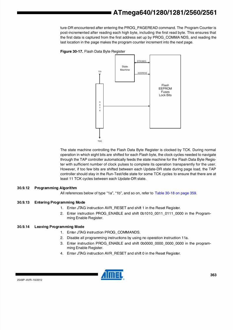
8/20/2019 At Mega 1281 Unlocked
http://slidepdf.com/reader/full/at-mega-1281-unlocked 363/446
363
2549P–AVR–10/2012
ATmega640/1280/1281/2560/2561
ture-DR encountered after entering the PROG_PAGEREAD command. The Program Counter is
post-incremented after reading each high byte, including the first read byte. This ensures tha
the first data is captured from the first address set up by PROG_COMMANDS, and reading the
last location in the page makes the program counter increment into the next page.
Figure 30-17. Flash Data Byte Register
The state machine controlling the Flash Data Byte Register is clocked by TCK. During norma
operation in which eight bits are shifted for each Flash byte, the clock cycles needed to navigate
through the TAP controller automatically feeds the state machine for the Flash Data Byte Regis-
ter with sufficient number of clock pulses to complete its operation transparently for the user
However, if too few bits are shifted between each Update-DR state during page load, the TAPcontroller should stay in the Run-Test/Idle state for some TCK cycles to ensure that there are a
least 11 TCK cycles between each Update-DR state.
30.9.12 Programming Algorithm
All references below of type “1a”, “1b”, and so on, refer to Table 30-18 on page 359.
30.9.13 Entering Programming Mode
1. Enter JTAG instruction AVR_RESET and shift 1 in the Reset Register.
2. Enter instruction PROG_ENABLE and shift 0b1010_0011_0111_0000 in the Program-ming Enable Register.
30.9.14 Leaving Programming Mode
1. Enter JTAG instruction PROG_COMMANDS.
2. Disable all programming instructions by using no operation instruction 11a.
3. Enter instruction PROG_ENABLE and shift 0b0000_0000_0000_0000 in the program-ming Enable Register.
4. Enter JTAG instruction AVR_RESET and shift 0 in the Reset Register.
TDI
TDO
D
A
T
A
FlashEEPROM
FusesLock Bits
STROBES
ADDRESS
State
Machine

8/20/2019 At Mega 1281 Unlocked
http://slidepdf.com/reader/full/at-mega-1281-unlocked 364/446
364
2549P–AVR–10/2012
ATmega640/1280/1281/2560/2561
30.9.15 Performing Chip Erase
1. Enter JTAG instruction PROG_COMMANDS.
2. Start Chip Erase using programming instruction 1a.
3. Poll for Chip Erase complete using programming instruction 1b, or wait for tWLRH_CE (refer
to Table 30-14 on page 348).
30.9.16 Programming the Flash
Before programming the Flash a Chip Erase must be performed, see “Performing Chip Erase”
on page 364.
1. Enter JTAG instruction PROG_COMMANDS.
2. Enable Flash write using programming instruction 2a.
3. Load address Extended High byte using programming instruction 2b.
4. Load address High byte using programming instruction 2c.
5. Load address Low byte using programming instruction 2d.
6. Load data using programming instructions 2e, 2f and 2g.
7. Repeat steps 5 and 6 for all instruction words in the page.
8. Write the page using programming instruction 2h.9. Poll for Flash write complete using programming instruction 2i, or wait for tWLRH (refer to
Table 30-14 on page 348).
10. Repeat steps 3 to 9 until all data have been programmed.
A more efficient data transfer can be achieved using the PROG_PAGELOAD instruction:
1. Enter JTAG instruction PROG_COMMANDS.
2. Enable Flash write using programming instruction 2a.
3. Load the page address using programming instructions 2b, 2c and 2d. PCWORD (referto Table 30-7 on page 338) is used to address within one page and must be written as 0.
4. Enter JTAG instruction PROG_PAGELOAD.
5. Load the entire page by shifting in all instruction words in the page byte-by-byte, startingwith the LSB of the first instruction in the page and ending with the MSB of the lastinstruction in the page. Use Update-DR to copy the contents of the Flash Data Byte Reg-ister into the Flash page location and to auto-increment the Program Counter beforeeach new word.
6. Enter JTAG instruction PROG_COMMANDS.
7. Write the page using programming instruction 2h.
8. Poll for Flash write complete using programming instruction 2i, or wait for tWLRH (refer toTable 30-14 on page 348).
9. Repeat steps 3 to 8 until all data have been programmed.
30.9.17 Reading the Flash
1. Enter JTAG instruction PROG_COMMANDS.
2. Enable Flash read using programming instruction 3a.
3. Load address using programming instructions 3b, 3c and 3d.
4. Read data using programming instruction 3e.
5. Repeat steps 3 and 4 until all data have been read.

8/20/2019 At Mega 1281 Unlocked
http://slidepdf.com/reader/full/at-mega-1281-unlocked 365/446
365
2549P–AVR–10/2012
ATmega640/1280/1281/2560/2561
A more efficient data transfer can be achieved using the PROG_PAGEREAD instruction:
1. Enter JTAG instruction PROG_COMMANDS.
2. Enable Flash read using programming instruction 3a.
3. Load the page address using programming instructions 3b, 3c and 3d. PCWORD (refer
to Table 30-7 on page 338) is used to address within one page and must be written as 0.4. Enter JTAG instruction PROG_PAGEREAD.
5. Read the entire page (or Flash) by shifting out all instruction words in the page (or Flash),starting with the LSB of the first instruction in the page (Flash) and ending with the MSBof the last instruction in the page (Flash). The Capture-DR state both captures the datafrom the Flash, and also auto-increments the program counter after each word is read.Note that Capture-DR comes before the shift-DR state. Hence, the first byte which isshifted out contains valid data.
6. Enter JTAG instruction PROG_COMMANDS.
7. Repeat steps 3 to 6 until all data have been read.
30.9.18 Programming the EEPROM
Before programming the EEPROM a Chip Erase must be performed, see “Performing ChipErase” on page 364.
1. Enter JTAG instruction PROG_COMMANDS.
2. Enable EEPROM write using programming instruction 4a.
3. Load address High byte using programming instruction 4b.
4. Load address Low byte using programming instruction 4c.
5. Load data using programming instructions 4d and 4e.
6. Repeat steps 4 and 5 for all data bytes in the page.
7. Write the data using programming instruction 4f.
8. Poll for EEPROM write complete using programming instruction 4g, or wait for tWLRH
(refer to Table 30-14 on page 348).9. Repeat steps 3 to 8 until all data have been programmed.
Note that the PROG_PAGELOAD instruction can not be used when programming the EEPROM
30.9.19 Reading the EEPROM
1. Enter JTAG instruction PROG_COMMANDS.
2. Enable EEPROM read using programming instruction 5a.
3. Load address using programming instructions 5b and 5c.
4. Read data using programming instruction 5d.
5. Repeat steps 3 and 4 until all data have been read.
Note that the PROG_PAGEREAD instruction can not be used when reading the EEPROM.
30.9.20 Programming the Fuses
1. Enter JTAG instruction PROG_COMMANDS.
2. Enable Fuse write using programming instruction 6a.
3. Load data high byte using programming instructions 6b. A bit value of “0” will program thecorresponding fuse, a “1” will unprogram the fuse.
4. Write Fuse High byte using programming instruction 6c.

8/20/2019 At Mega 1281 Unlocked
http://slidepdf.com/reader/full/at-mega-1281-unlocked 366/446
366
2549P–AVR–10/2012
ATmega640/1280/1281/2560/2561
5. Poll for Fuse write complete using programming instruction 6d, or wait for tWLRH (refer to
Table 30-14 on page 348).
6. Load data low byte using programming instructions 6e. A “0” will program the fuse, a “1”will unprogram the fuse.
7. Write Fuse low byte using programming instruction 6f.
8. Poll for Fuse write complete using programming instruction 6g, or wait for tWLRH (refer to
Table 30-14 on page 348).
30.9.21 Programming the Lock Bits
1. Enter JTAG instruction PROG_COMMANDS.
2. Enable Lock bit write using programming instruction 7a.
3. Load data using programming instructions 7b. A bit value of “0” will program the corre-sponding lock bit, a “1” will leave the lock bit unchanged.
4. Write Lock bits using programming instruction 7c.
5. Poll for Lock bit write complete using programming instruction 7d, or wait for tWLRH (refer
to Table 30-14 on page 348).
30.9.22 Reading the Fuses and Lock Bits1. Enter JTAG instruction PROG_COMMANDS.
2. Enable Fuse/Lock bit read using programming instruction 8a.
3. To read all Fuses and Lock bits, use programming instruction 8e.To only read Fuse High byte, use programming instruction 8b.To only read Fuse Low byte, use programming instruction 8c.To only read Lock bits, use programming instruction 8d.
30.9.23 Reading the Signature Bytes
1. Enter JTAG instruction PROG_COMMANDS.
2. Enable Signature byte read using programming instruction 9a.
3. Load address 0x00 using programming instruction 9b.4. Read first signature byte using programming instruction 9c.
5. Repeat steps 3 and 4 with address 0x01 and address 0x02 to read the second and thirdsignature bytes, respectively.
30.9.24 Reading the Calibration Byte
1. Enter JTAG instruction PROG_COMMANDS.
2. Enable Calibration byte read using programming instruction 10a.
3. Load address 0x00 using programming instruction 10b.
4. Read the calibration byte using programming instruction 10c.

8/20/2019 At Mega 1281 Unlocked
http://slidepdf.com/reader/full/at-mega-1281-unlocked 367/446
367
2549P–AVR–10/2012
ATmega640/1280/1281/2560/2561
31. Electrical Characteristics
Absolute Maximum Ratings*
31.1 DC Characteristics
Operating Temperature.................................. -55°C to +125°C *NOTICE: Stresses beyond those listed under “Absolute
Maximum Ratings” may cause permanent dam-
age to the device. This is a stress rating only and
functional operation of the device at these orother conditions beyond those indicated in the
operational sections of this specification is not
implied. Exposure to absolute maximum rating
conditions for extended periods may affect
device reliability.
Storage Temperature..................................... -65°C to +150°C
Voltage on any Pin except RESETwith respect to Ground ................................-0.5V to VCC+0.5V
Voltage on RESET with respect to Ground...... -0.5V to +13.0V
Maximum Operating Voltage ............................................ 6.0V
DC Current per I/O Pin ................................................ 40.0mA
DC Current VCC and GND Pins................................. 200.0mA
TA = -40°C to 85°C, VCC = 1.8V to 5.5V (unless otherwise noted)Symbol Parameter Condition Min. Typ. Max. Units
VILInput Low Voltage, ExceptXTAL1 and Reset pin
VCC = 1.8V - 2.4VVCC = 2.4V - 5.5V
-0.5-0.5
0.2VCC(1)
0.3VCC(1)
V
VIL1Input Low Voltage,XTAL1 pin
VCC = 1.8V - 5.5V -0.5 0.1VCC(1)
VIL2Input Low Voltage,RESET pin
VCC = 1.8V - 5.5V -0.5 0.1VCC(1)
VIH
Input High Voltage,Except XTAL1 andRESET pins
VCC = 1.8V - 2.4VVCC = 2.4V - 5.5V
0.7VCC(2)
0.6VCC(2)
VCC + 0.5VCC + 0.5
VIH1Input High Voltage,XTAL1 pin
VCC = 1.8V - 2.4VVCC = 2.4V - 5.5V
0.8VCC(2)
0.7VCC(2)
VCC + 0.5VCC + 0.5
VIH2Input High Voltage,RESET pin
VCC = 1.8V - 5.5V 0.9VCC(2) VCC + 0.5
VOLOutput Low Voltage(3),Except RESET pin
IOL = 20mA, VCC = 5VIOL = 10mA, VCC = 3V
0.90.6
VOHOutput High Voltage(4),Except RESET pin
IOH = -20mA, VCC = 5VIOH = -10mA, VCC = 3V
4.22.3
IILInput LeakageCurrent I/O Pin
VCC = 5.5V, pin low(absolute value)
1
µA
IIH
Input Leakage
Current I/O Pin
VCC = 5.5V, pin high
(absolute value)1
RRST Reset Pull-up Resistor 30 60kΩ
RPU I/O Pin Pull-up Resistor 20 50
8/20/2019 At Mega 1281 Unlocked
http://slidepdf.com/reader/full/at-mega-1281-unlocked 368/446
368
2549P–AVR–10/2012
ATmega640/1280/1281/2560/2561
Notes: 1. "Max" means the highest value where the pin is guaranteed to be read as low.
2. "Min" means the lowest value where the pin is guaranteed to be read as high.
3. Although each I/O port can sink more than the test conditions (20mA at VCC = 5V, 10mA at VCC = 3V) under steady stateconditions (non-transient), the following must be observed:ATmega1281/2561:
1.)The sum of all IOL, for ports A0-A7, G2, C4-C7 should not exceed 100mA.2.)The sum of all IOL, for ports C0-C3, G0-G1, D0-D7 should not exceed 100mA.3.)The sum of all IOL, for ports G3-G5, B0-B7, E0-E7 should not exceed 100mA.4.)The sum of all IOL, for ports F0-F7 should not exceed 100mA.ATmega640/1280/2560:1.)The sum of all IOL, for ports J0-J7, A0-A7, G2 should not exceed 200mA.2.)The sum of all IOL, for ports C0-C7, G0-G1, D0-D7, L0-L7 should not exceed 200mA.3.)The sum of all IOL, for ports G3-G4, B0-B7, H0-B7 should not exceed 200mA.4.)The sum of all IOL, for ports E0-E7, G5 should not exceed 100mA.5.)The sum of all IOL, for ports F0-F7, K0-K7 should not exceed 100mA.If IOL exceeds the test condition, VOL may exceed the related specification. Pins are not guaranteed to sink current greaterthan the listed test condition.
4. Although each I/O port can source more than the test conditions (20mA at VCC = 5V, 10mA at VCC = 3V) under steadystate conditions (non-transient), the following must be observed:
ATmega1281/2561:1)The sum of all IOH, for ports A0-A7, G2, C4-C7 should not exceed 100mA.2)The sum of all IOH, for ports C0-C3, G0-G1, D0-D7 should not exceed 100mA.3)The sum of all IOH, for ports G3-G5, B0-B7, E0-E7 should not exceed 100mA.4)The sum of all IOH, for ports F0-F7 should not exceed 100mA.ATmega640/1280/2560:1)The sum of all IOH, for ports J0-J7, G2, A0-A7 should not exceed 200mA.2)The sum of all IOH, for ports C0-C7, G0-G1, D0-D7, L0-L7 should not exceed 200mA.3)The sum of all IOH, for ports G3-G4, B0-B7, H0-H7 should not exceed 200mA.4)The sum of all IOH, for ports E0-E7, G5 should not exceed 100mA.
ICC
Power Supply Current(5)
Active 1MHz, VCC = 2V(ATmega640/1280/2560/1V)
0.5 0.8
mA
Active 4MHz, VCC = 3V
(ATmega640/1280/2560/1L)
3.2 5
Active 8MHz, VCC = 5V(ATmega640/1280/1281/2560/2561)
10 14
Idle 1MHz, VCC = 2V(ATmega640/1280/2560/1V)
0.14 0.22
Idle 4MHz, VCC = 3V(ATmega640/1280/2560/1L)
0.7 1.1
Idle 8MHz, VCC = 5V(ATmega640/1280/1281/2560/2561)
2.7 4
Power-down modeWDT enabled, VCC = 3V <5 15
µAWDT disabled, VCC = 3V <1 7.5
VACIOAnalog ComparatorInput Offset Voltage
VCC = 5VVin = VCC /2
<10 40 mV
IACLKAnalog ComparatorInput Leakage Current
VCC = 5VVin = VCC /2
-50 50 nA
tACIDAnalog ComparatorPropagation Delay
VCC = 2.7VVCC = 4.0V
750500
ns
TA = -40°C to 85°C, VCC = 1.8V to 5.5V (unless otherwise noted) (Continued)
Symbol Parameter Condition Min. Typ. Max. Units

8/20/2019 At Mega 1281 Unlocked
http://slidepdf.com/reader/full/at-mega-1281-unlocked 369/446
369
2549P–AVR–10/2012
ATmega640/1280/1281/2560/2561
5)The sum of all IOH, for ports F0-F7, K0-K7 should not exceed 100mA.If IOH exceeds the test condition, VOH may exceed the related specification. Pins are not guaranteed to source currentgreater than the listed test condition.
5. Values with “PRR1 – Power Reduction Register 1” enabled (0xFF).
31.2 Speed Grades
Maximum frequency is depending on VCC. As shown in Figure 31-1 trough Figure 31-4 on page370, the Maximum Frequency vs. VCC curve is linear between 1.8V < VCC < 2.7V and between
2.7V < VCC < 4.5V.
31.2.1 8MHz
Figure 31-1. Maximum Frequency vs. VCC, ATmega640V/1280V/1281V/2560V/2561V
Figure 31-2. Maximum Frequency vs. VCC when also No-Read-While-Write Section(1),ATmega2560V/ATmega2561V, is used
Note: 1. When only using the Read-While-Write Section of the program memory, a higher speed canbe achieved at low voltage, see “Read-While-Write and No Read-While-Write Flash Sections”
on page 317 for addresses.
8 MHz
4 MHz
1.8V 2.7V 5.5V
Safe Operating Area
8 MHz
2 MHz
1.8V 2.7V 5.5V
Safe Operating Area
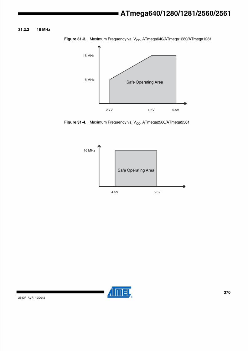
8/20/2019 At Mega 1281 Unlocked
http://slidepdf.com/reader/full/at-mega-1281-unlocked 370/446
370
2549P–AVR–10/2012
ATmega640/1280/1281/2560/2561
31.2.2 16 MHz
Figure 31-3. Maximum Frequency vs. VCC, ATmega640/ATmega1280/ATmega1281
Figure 31-4. Maximum Frequency vs. VCC, ATmega2560/ATmega2561
16 MHz
8 MHz
2.7V 4.5V 5.5V
Safe Operating Area
16 MHz
4.5V 5.5V
Safe Operating Area

8/20/2019 At Mega 1281 Unlocked
http://slidepdf.com/reader/full/at-mega-1281-unlocked 371/446
371
2549P–AVR–10/2012
ATmega640/1280/1281/2560/2561
31.3 Clock Characteristics
31.3.1 Calibrated Internal RC Oscillator Accuracy
Notes: 1. Voltage range for ATmega640V/1281V/1280V/2561V/2560V.
2. Voltage range for ATmega640/1281/1280/2561/2560.
31.3.2 External Clock Drive Waveforms
Figure 31-5. External Clock Drive Waveforms
31.4 External Clock Drive
Table 31-1. Calibration Accuracy of Internal RC Oscillator
Frequency VCC Temperature Calibration Accuracy
Factory Calibration 8.0MHz 3V 25°C ±10%
User Calibration 7.3MHz - 8.1MHz1.8V - 5.5V(1)
2.7V - 5.5V(2) -40°C - 85°C ±1%
VIL1
VIH1
Table 31-2. External Clock Drive
Symbol Parameter
VCC = 1.8V - 5.5V VCC = 2.7V - 5.5V VCC = 4.5V - 5.5V
UnitsMin. Max. Min. Max. Min. Max.
1/tCLCLOscillatorFrequency
0 2 0 8 0 16 MHz
tCLCL Clock Period 500 125 62.5
nstCHCX High Time 200 50 25
tCLCX Low Time 200 50 25
tCLCH
Rise Time 2.0 1.6 0.5
μstCHCL Fall Time 2.0 1.6 0.5
ΔtCLCL
Change in periodfrom one clockcycle to the next
2 2 2 %

8/20/2019 At Mega 1281 Unlocked
http://slidepdf.com/reader/full/at-mega-1281-unlocked 372/446
372
2549P–AVR–10/2012
ATmega640/1280/1281/2560/2561
31.5 System and Reset Characteristics
Note: 1. The Power-on Reset will not work unless the supply voltage has been below VPOT (falling).
31.5.1 Standard Power-On ResetThis imp lementa t ion o f power -on rese t ex is ted in ear ly vers ions o
ATmega640/1280/1281/2560/2561. The table below describes the characteristics of this power
on reset and it is valid for the following devices only:
• ATmega640: revision A
• ATmega1280: revision A
• ATmega1281: revision A
• ATmega2560: revision A to E
• ATmega2561: revision A to E
Table 31-4. Characteristics of Standard Power-On Reset. TA= -40 to +85°C.
Notes: 1. Values are guidelines only.2. Threshold where device is released from reset when voltage is rising.3. The power-on reset threshold voltage (falling) will not work unless the supply voltage has been
below VPOT.
Table 31-3. Reset, Brown-out and Internal voltage CharacteristicsCharacteristics
Symbol Parameter Condition Min Typ Max UnitsVRST RESET Pin Threshold Voltage 0.2VCC 0.9VCC V
tRST Minimum pulse width on RESET Pin 2.5 µs
VHYST Brown-out Detector Hysteresis 50 mV
tBOD Min Pulse Width on Brown-out Reset 2 µs
VBG Bandgap reference voltage VCC=2.7V, TA= 25°C 1.0 1.1 1.2 V
tBG Bandgap reference start-up time VCC=2.7V, TA= 25°C 40 70 µs
IBG Bandgap reference current consumption VCC=2.7V, TA= 25°C 10 µA
Symbol Parameter Min.(1) Typ.(1) Max.(1) Units
VPOT
Power-on Reset Threshold Voltage (rising)(2) 0.7 1.0 1.4 V
Power-on Reset Threshold Voltage (falling)(3) 0.05 0.9 1.3 V
VPSR Power-on slope rate 0.01 4.5 V/ms
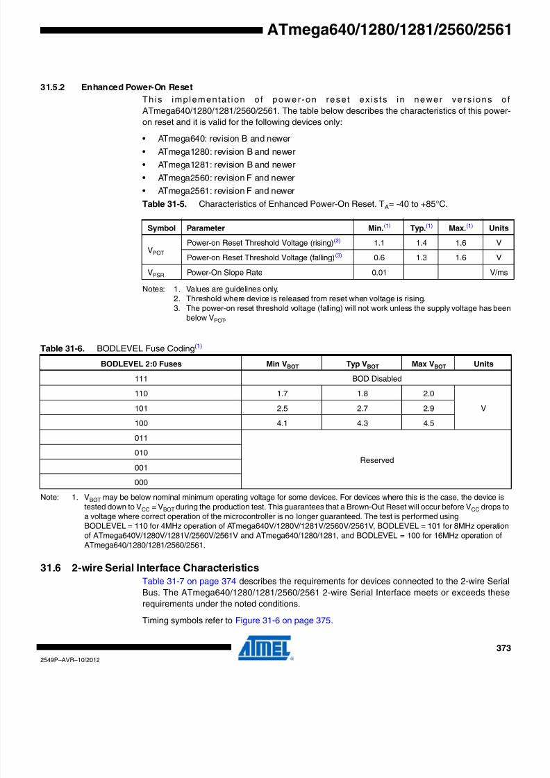
8/20/2019 At Mega 1281 Unlocked
http://slidepdf.com/reader/full/at-mega-1281-unlocked 373/446
373
2549P–AVR–10/2012
ATmega640/1280/1281/2560/2561
31.5.2 Enhanced Power-On Reset
This imp lementa t ion o f power -on rese t ex is t s in newer vers ions o f
ATmega640/1280/1281/2560/2561. The table below describes the characteristics of this power
on reset and it is valid for the following devices only:
• ATmega640: revision B and newer
• ATmega1280: revision B and newer
• ATmega1281: revision B and newer
• ATmega2560: revision F and newer
• ATmega2561: revision F and newer
Table 31-5. Characteristics of Enhanced Power-On Reset. TA= -40 to +85°C.
Notes: 1. Values are guidelines only.2. Threshold where device is released from reset when voltage is rising.3. The power-on reset threshold voltage (falling) will not work unless the supply voltage has been
below VPOT.
Note: 1. VBOT may be below nominal minimum operating voltage for some devices. For devices where this is the case, the device istested down to VCC = VBOT during the production test. This guarantees that a Brown-Out Reset will occur before VCC drops toa voltage where correct operation of the microcontroller is no longer guaranteed. The test is performed usingBODLEVEL = 110 for 4MHz operation of ATmega640V/1280V/1281V/2560V/2561V, BODLEVEL = 101 for 8MHz operationof ATmega640V/1280V/1281V/2560V/2561V and ATmega640/1280/1281, and BODLEVEL = 100 for 16MHz operation ofATmega640/1280/1281/2560/2561.
31.6 2-wire Serial Interface Characteristics
Table 31-7 on page 374 describes the requirements for devices connected to the 2-wire Seria
Bus. The ATmega640/1280/1281/2560/2561 2-wire Serial Interface meets or exceeds these
requirements under the noted conditions.
Timing symbols refer to Figure 31-6 on page 375.
Symbol Parameter Min.(1) Typ.(1) Max.(1) Units
VPOT
Power-on Reset Threshold Voltage (rising)(2) 1.1 1.4 1.6 V
Power-on Reset Threshold Voltage (falling)(3) 0.6 1.3 1.6 V
VPSR Power-On Slope Rate 0.01 V/ms
Table 31-6. BODLEVEL Fuse Coding(1)
BODLEVEL 2:0 Fuses Min VBOT Typ VBOT Max VBOT Units
111 BOD Disabled
110 1.7 1.8 2.0
V101 2.5 2.7 2.9
100 4.1 4.3 4.5
011
Reserved010
001
000
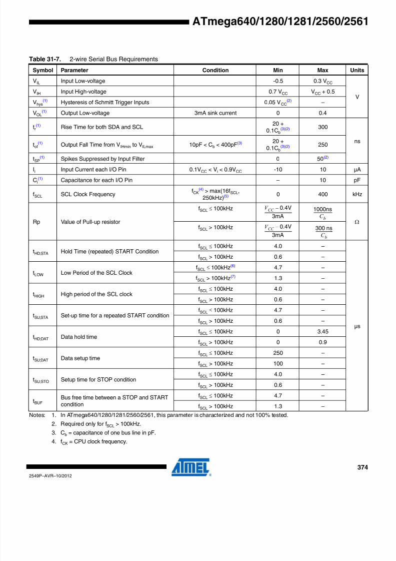
8/20/2019 At Mega 1281 Unlocked
http://slidepdf.com/reader/full/at-mega-1281-unlocked 374/446
374
2549P–AVR–10/2012
ATmega640/1280/1281/2560/2561
Notes: 1. In ATmega640/1280/1281/2560/2561, this parameter is characterized and not 100% tested.
2. Required only for fSCL > 100kHz.
3. Cb = capacitance of one bus line in pF.
4. fCK = CPU clock frequency.
Table 31-7. 2-wire Serial Bus Requirements
Symbol Parameter Condition Min Max Units
VIL Input Low-voltage -0.5 0.3 VCC
VVIH Input High-voltage 0.7 VCC VCC + 0.5
Vhys(1) Hysteresis of Schmitt Trigger Inputs 0.05 VCC
(2) –
VOL(1) Output Low-voltage 3mA sink current 0 0.4
tr(1) Rise Time for both SDA and SCL
20 +0.1Cb
(3)(2) 300
nstof
(1) Output Fall Time from VIHmin to VILmax 10pF < Cb < 400pF(3) 20 +0.1Cb
(3)(2) 250
tSP(1) Spikes Suppressed by Input Filter 0 50(2)
Ii Input Current each I/O Pin 0.1VCC < Vi < 0.9VCC -10 10 µA
Ci(1) Capacitance for each I/O Pin – 10 pF
fSCL SCL Clock Frequency fCK(4)
> max(16fSCL,250kHz)(5) 0 400 kHz
Rp Value of Pull-up resistor
fSCL ≤ 100kHz
fSCL > 100kHz
tHD;STA Hold Time (repeated) START ConditionfSCL ≤ 100kHz 4.0 –
µs
fSCL > 100kHz 0.6 –
tLOW Low Period of the SCL ClockfSCL ≤ 100kHz(6) 4.7 –
fSCL > 100kHz(7) 1.3 –
tHIGH High period of the SCL clockfSCL ≤ 100kHz 4.0 –
fSCL > 100kHz 0.6 –
tSU;STA Set-up time for a repeated START conditionfSCL ≤ 100kHz 4.7 –
fSCL > 100kHz 0.6 –
tHD;DAT Data hold timefSCL ≤ 100kHz 0 3.45
fSCL > 100kHz 0 0.9
tSU;DAT Data setup timefSCL ≤ 100kHz 250 –
fSCL > 100kHz 100 –
tSU;STO Setup time for STOP conditionfSCL ≤ 100kHz 4.0 –
fSCL > 100kHz 0.6 –
tBUFBus free time between a STOP and STARTcondition
fSCL ≤ 100kHz 4.7 –
fSCL > 100kHz 1.3 –
V CC 0.4V–
3mA----------------------------
1000nsC b
-------------------
ΩV CC 0.4V–
3mA----------------------------
300 nsC b
------------------

8/20/2019 At Mega 1281 Unlocked
http://slidepdf.com/reader/full/at-mega-1281-unlocked 375/446
375
2549P–AVR–10/2012
ATmega640/1280/1281/2560/2561
5. This requirement applies to all ATmega640/1280/1281/2560/2561 2-wire Serial Interface operation. Other devices con-nected to the 2-wire Serial Bus need only obey the general fSCL requirement.
6. The actual low period generated by the ATmega640/1280/1281/2560/2561 2-wire Serial Interface is (1/fSCL - 2/fCK), thus fCK
must be greater than 6MHz for the low time requirement to be strictly met at fSCL = 100kHz.
7. The actual low period generated by the ATmega640/1280/1281/2560/2561 2-wire Serial Interface is (1/fSCL - 2/fCK), thus thelow time requirement will not be strictly met for fSCL > 308kHz when fCK = 8MHz. Still, ATmega640/1280/1281/2560/2561devices connected to the bus may communicate at full speed (400kHz) with other ATmega640/1280/1281/2560/2561devices, as well as any other device with a proper tLOW acceptance margin.
Figure 31-6. 2-wire Serial Bus Timing
31.7 SPI Timing Characteristics
See Figure 31-7 on page 376 and Figure 31-8 on page 376 for details.
Note: 1. In SPI Programming mode the minimum SCK high/low period is:- 2 tCLCL for fCK < 12MHz- 3 tCLCL for fCK > 12MHz
tSU;STA
tLOW
tHIGH
tLOW
tof
tHD;STA tHD;DAT tSU;DATtSU;STO
tBUF
SCL
SDA
tr
Table 31-8. SPI Timing Parameters
Description Mode Min Typ Max
1 SCK period MasterSee Table 21-5 on
page 203
ns
2 SCK high/low Master 50% duty cycle
3 Rise/Fall time Master 3.6
4 Setup Master 10
5 Hold Master 10
6 Out to SCK Master 0.5 • tsck
7 SCK to out Master 10
8 SCK to out high Master 10
9 SS low to out Slave 15
10 SCK period Slave 4 • tck
11 SCK high/low(1) Slave 2 • tck
12 Rise/Fall time Slave 1600
13 Setup Slave 10
14 Hold Slave tck
15 SCK to out Slave 15
16 SCK to SS high Slave 20
17 SS high to tri-state Slave 10
18 SS low to SCK Slave 20

8/20/2019 At Mega 1281 Unlocked
http://slidepdf.com/reader/full/at-mega-1281-unlocked 376/446
376
2549P–AVR–10/2012
ATmega640/1280/1281/2560/2561
Figure 31-7. SPI Interface Timing Requirements (Master Mode)
Figure 31-8. SPI Interface Timing Requirements (Slave Mode)
MOSI
(Data Output)
SCK
(CPOL = 1)
MISO
(Data Input)
SCK
(CPOL = 0)
SS
MSB LSB
LSBMSB
...
...
6 1
2 2
34 5
87
MISO
(Data Output)
SCK
(CPOL = 1)
MOSI
(Data Input)
SCK
(CPOL = 0)
SS
MSB LSB
LSBMSB
...
...
10
11 11
1213 14
1715
9
X
16

8/20/2019 At Mega 1281 Unlocked
http://slidepdf.com/reader/full/at-mega-1281-unlocked 377/446
377
2549P–AVR–10/2012
ATmega640/1280/1281/2560/2561
31.8 ADC Characteristics – Preliminary Data
Note: 1. Values are guidelines only.
Table 31-9. ADC Characteristics, Singel Ended Channels
Symbol Parameter Condition Min(1) Typ(1) Max(1) Units
Resolution Single Ended Conversion 10 Bits
Absolute accuracy (IncludingINL, DNL, quantization error,gain and offset error)
Single Ended Conversion
VREF = 4V, VCC = 4V,CLKADC= 200kHz
2.25 2.5
LSB
Single Ended ConversionVREF = 4V, VCC = 4V,CLKADC = 1MHz
3
Single Ended ConversionVREF = 4V, VCC = 4V,CLKADC = 200kHzNoise Reduction Mode
2
Single Ended ConversionVREF = 4V, VCC = 4V,CLKADC = 1MHz
Noise Reduction Mode
3
Integral Non-Linearity (INL)Single Ended ConversionVREF = 4V, VCC = 4V,CLKADC = 200kHz
1.25
Differential Non-Linearity (DNL)Single Ended ConversionVREF = 4V, VCC = 4V,CLKADC = 200kHz
0.5
Gain ErrorSingle Ended ConversionVREF = 4V, VCC = 4V,CLKADC= 200kHz
2
Offset ErrorSingle Ended ConversionVREF = 4V, VCC = 4V,
CLKADC = 200kHz
-2
Conversion Time Free Running Conversion 13 260 µs
Clock Frequency Single Ended Conversion 50 1000 kHz
AVCC Analog Supply Voltage VCC - 0.3 VCC + 0.3
VVREF Reference Voltage 1.0 AVCC
VIN Input Voltage GND VREF
Input Bandwidth 38,5 kHz
VINT1 Internal Voltage Reference 1.1V 1.0 1.1 1.2V
VINT2 Internal Voltage Reference 2.56V 2.4 2.56 2.8
RREF Reference Input Resistance 32 kΩ
RAIN Analog Input Resistance 100 MΩ

8/20/2019 At Mega 1281 Unlocked
http://slidepdf.com/reader/full/at-mega-1281-unlocked 378/446
378
2549P–AVR–10/2012
ATmega640/1280/1281/2560/2561
Table 31-10. ADC Characteristics, Differential Channels
Symbol Parameter Condition Min(1) Typ(1) Max(1) Units
Resolution
Gain = 1× 8
BitsGain = 10× 8
Gain = 200× 7
Absolute Accuracy(Including INL, DNL,Quantization Error, Gain and Offset Error)
Gain = 1×VREF = 4V, VCC = 5VCLKADC = 50 - 200kHz
18
LSB
Gain = 10×VREF = 4V, VCC = 5VCLKADC = 50 - 200kHz
17
Gain = 200×VREF = 4V, VCC = 5VCLKADC = 50 - 200kHz
9
Integral Non-Linearity (INL)
Gain = 1×VREF = 4V, VCC = 5VCLK
ADC = 50 - 200kHz
2.5
Gain = 10×VREF = 4V, VCC = 5VCLKADC = 50 - 200kHz
5
Gain = 200×VREF = 4V, VCC = 5VCLKADC = 50 - 200kHz
9
Differential Non-Linearity (DNL)
Gain = 1×VREF = 4V, VCC = 5VCLKADC = 50 - 200kHz
0.75
Gain = 10×VREF = 4V, VCC = 5V
CLKADC = 50 - 200kHz
1.5
Gain = 200×VREF = 4V, VCC = 5VCLKADC = 50 - 200kHz
10
Gain Error
Gain = 1× 1.7
%Gain = 10× 1.7
Gain = 200× 0.5
Offset Error
Gain = 1×VREF = 4V, VCC = 5VCLKADC = 50 - 200kHz
2
LSB
Gain = 10×
VREF = 4V, VCC = 5VCLKADC = 50 - 200kHz
2
Gain = 200×VREF = 4V, VCC = 5VCLKADC = 50 - 200kHz
3
Clock Frequency 50 200 kHz
Conversion Time 65 260 µs

8/20/2019 At Mega 1281 Unlocked
http://slidepdf.com/reader/full/at-mega-1281-unlocked 379/446
379
2549P–AVR–10/2012
ATmega640/1280/1281/2560/2561
Note: Values are guidelines only.
31.9 External Data Memory Timing
Notes: 1. This assumes 50% clock duty cycle. The half period is actually the high time of the external clock, XTAL1.
2. This assumes 50% clock duty cycle. The half period is actually the low time of the external clock, XTAL1.
AVCC Analog Supply Voltage VCC - 0.3 VCC + 0.3
VVREF Reference Voltage 2.7 AVCC - 0.5
VIN Input Voltage GND VCC
VDIFF Input Differential Voltage -VREF /Gain VREF /Gain
ADC Conversion Output -511 511 LSB
Input Bandwidth 4 kHz
VINT Internal Voltage Reference 2.3 2.56 2.8 V
RREF Reference Input Resistance 32 kΩ
RAIN Analog Input Resistance 100 MΩ
Table 31-11. External Data Memory Characteristics, 4.5 to 5.5 Volts, No Wait-state
Symbol Parameter
8MHz Oscillator Variable Oscillator
UnitMin Max Min Max
0 1/tCLCL Oscillator Frequency 0.0 16 MHz
1 tLHLL ALE Pulse Width 115 1.0tCLCL-10
ns
2 tAVLL Address Valid A to ALE Low 57.5 0.5tCLCL-5(1)
3a tLLAX_STAddress Hold After ALE Low,write access
5 5
3b tLLAX_LDAddress Hold after ALE Low,
read access
5 5
4 tAVLLC Address Valid C to ALE Low 57.5 0.5tCLCL-5(1)
5 tAVRL Address Valid to RD Low 115 1.0tCLCL-10
6 tAVWL Address Valid to WR Low 115 1.0tCLCL-10
7 tLLWL ALE Low to WR Low 47.5 67.5 0.5tCLCL-15(2) 0.5tCLCL+5(2)
8 tLLRL ALE Low to RD Low 47.5 67.5 0.5tCLCL-15(2) 0.5tCLCL+5(2)
9 tDVRH Data Setup to RD High 40 40
10 tRLDV Read Low to Data Valid 75 1.0tCLCL-50
11 tRHDX Data Hold After RD High 0 0
12 tRLRH RD PulseW
idth 115 1.0tCLCL-1013 tDVWL Data Setup to WR Low 42.5 0.5tCLCL-20(1)
14 tWHDX Data Hold After WR High 115 1.0tCLCL-10
15 tDVWH Data Valid to WR High 125 1.0tCLCL
16 tWLWH WR Pulse Width 115 1.0tCLCL-10
Table 31-10. ADC Characteristics, Differential Channels (Continued)
Symbol Parameter Condition Min(1) Typ(1) Max(1) Units

8/20/2019 At Mega 1281 Unlocked
http://slidepdf.com/reader/full/at-mega-1281-unlocked 380/446
380
2549P–AVR–10/2012
ATmega640/1280/1281/2560/2561
Table 31-12. External Data Memory Characteristics, 4.5 to 5.5 Volts, 1 Cycle Wait-state
Symbol Parameter
8MHz Oscillator Variable Oscillator
UnitMin Max Min Max
0 1/tCLCL Oscillator Frequency 0.0 16 MHz
10 tRLDV Read Low to Data Valid 200 2.0tCLCL-50
ns12 tRLRH RD Pulse Width 240 2.0tCLCL-10
15 tDVWH Data Valid to WR High 240 2.0tCLCL
16 tWLWH WR Pulse Width 240 2.0tCLCL-10
Table 31-13. External Data Memory Characteristics, 4.5 to 5.5 Volts, SRWn1 = 1, SRWn0 = 0
Symbol Parameter
4MHz Oscillator Variable Oscillator
UnitMin Max Min Max
0 1/tCLCL Oscillator Frequency 0.0 16 MHz
10 tRLDV Read Low to Data Valid 325 3.0tCLCL-50
ns12 tRLRH RD Pulse Width 365 3.0tCLCL-10
15 tDVWH Data Valid to WR High 375 3.0tCLCL
16 tWLWH WR Pulse Width 365 3.0tCLCL-10
Table 31-14. External Data Memory Characteristics, 4.5 to 5.5 Volts, SRWn1 = 1, SRWn0 = 1
Symbol Parameter
4MHz Oscillator Variable Oscillator
UnitMin Max Min Max
0 1/tCLCL Oscillator Frequency 0.0 16 MHz10 tRLDV Read Low to Data Valid 325 3.0tCLCL-50
ns
12 tRLRH RD Pulse Width 365 3.0tCLCL-10
14 tWHDX Data Hold After WR High 240 2.0tCLCL-10
15 tDVWH Data Valid to WR High 375 3.0tCLCL
16 tWLWH WR Pulse Width 365 3.0tCLCL-10
Table 31-15. External Data Memory Characteristics, 2.7 to 5.5 Volts, No Wait-state
Symbol Parameter
4MHz Oscillator Variable Oscillator
UnitMin Max Min Max
0 1/tCLCL Oscillator Frequency 0.0 8 MHz

8/20/2019 At Mega 1281 Unlocked
http://slidepdf.com/reader/full/at-mega-1281-unlocked 381/446
381
2549P–AVR–10/2012
ATmega640/1280/1281/2560/2561
Notes: 1. This assumes 50% clock duty cycle. The half period is actually the high time of the external clock, XTAL1.2. This assumes 50% clock duty cycle. The half period is actually the low time of the external clock, XTAL1.
1 tLHLL ALE Pulse Width 235 tCLCL-15
ns
2 tAVLL Address Valid A to ALE Low 115 0.5tCLCL-10(1)
3a tLLAX_STAddress Hold After ALE Low,write access
5 5
3b tLLAX_LDAddress Hold after ALE Low,read access
5 5
4 tAVLLC Address Valid C to ALE Low 115 0.5tCLCL-10(1)
5 tAVRL Address Valid to RD Low 235 1.0tCLCL-15
6 tAVWL Address Valid to WR Low 235 1.0tCLCL-15
7 tLLWL ALE Low to WR Low 115 130 0.5tCLCL-10(2) 0.5tCLCL+5(2)
8 tLLRL ALE Low to RD Low 115 130 0.5tCLCL-10(2) 0.5tCLCL+5(2)
9 tDVRH Data Setup to RD High 45 4510 tRLDV Read Low to Data Valid 190 1.0tCLCL-60
11 tRHDX Data Hold After RD High 0 0
12 tRLRH RD Pulse Width 235 1.0tCLCL-15
13 tDVWL Data Setup to WR Low 105 0.5tCLCL-20(1)
14 tWHDX Data Hold After WR High 235 1.0tCLCL-15
15 tDVWH Data Valid to WR High 250 1.0tCLCL
16 tWLWH WR Pulse Width 235 1.0tCLCL-15
Table 31-15. External Data Memory Characteristics, 2.7 to 5.5 Volts, No Wait-state (Continued)
Symbol Parameter
4MHz Oscillator Variable Oscillator
UnitMin Max Min Max
Table 31-16. External Data Memory Characteristics, 2.7 to 5.5 Volts, SRWn1 = 0, SRWn0 = 1
Symbol Parameter
4MHz Oscillator Variable Oscillator
UnitMin Max Min Max
0 1/tCLCL Oscillator Frequency 0.0 8 MHz
10 tRLDV Read Low to Data Valid 440 2.0tCLCL-60
ns12 tRLRH RD Pulse Width 485 2.0tCLCL-15
15 tDVWH Data Valid to WR High 500 2.0tCLCL
16 tWLWH WR Pulse Width 485 2.0tCLCL-15

8/20/2019 At Mega 1281 Unlocked
http://slidepdf.com/reader/full/at-mega-1281-unlocked 382/446
382
2549P–AVR–10/2012
ATmega640/1280/1281/2560/2561
Figure 31-9. External Memory Timing (SRWn1 = 0, SRWn0 = 0
Table 31-17. External Data Memory Characteristics, 2.7 to 5.5 Volts, SRWn1 = 1, SRWn0 = 0
Symbol Parameter
4MHz Oscillator Variable Oscillator
UnitMin Max Min Max
0 1/tCLCL Oscillator Frequency 0.0 8 MHz
10 tRLDV Read Low to Data Valid 690 3.0tCLCL-60
ns12 tRLRH RD Pulse Width 735 3.0tCLCL-15
15 tDVWH Data Valid to WR High 750 3.0tCLCL
16 tWLWH WR Pulse Width 735 3.0tCLCL-15
Table 31-18. External Data Memory Characteristics, 2.7 to 5.5 Volts, SRWn1 = 1, SRWn0 = 1
Symbol Parameter
4MHz Oscillator Variable Oscillator
UnitMin Max Min Max
0 1/tCLCL Oscillator Frequency 0.0 8 MHz
10 tRLDV Read Low to Data Valid 690 3.0tCLCL-60
ns
12 tRLRH RD Pulse Width 735 3.0tCLCL-15
14 tWHDX Data Hold After WR High 485 2.0tCLCL-15
15 tDVWH Data Valid to WR High 750 3.0tCLCL
16 tWLWH WR Pulse Width 735 3.0tCLCL-15
ALE
T1 T2 T3
W r i t e
R e a
d
WR
T4
A15:8 AddressPrev. addr.
DA7:0 Address DataPrev. data XX
RD
DA7:0 (XMBK = 0) DataAddress
System Clock (CLKCPU)
1
4
2
7
6
3a
3b
5
8 12
16
13
10
11
14
15
9

8/20/2019 At Mega 1281 Unlocked
http://slidepdf.com/reader/full/at-mega-1281-unlocked 383/446
383
2549P–AVR–10/2012
ATmega640/1280/1281/2560/2561
Figure 31-10. External Memory Timing (SRWn1 = 0, SRWn0 = 1)
Figure 31-11. External Memory Timing (SRWn1 = 1, SRWn0 = 0)
ALE
T1 T2 T3
W r i t e
R e a d
WR
T5
A15:8 AddressPrev. addr.
DA7:0 Address DataPrev. data XX
RD
DA7:0 (XMBK = 0) DataAddress
System Clock (CLKCPU)
1
4
2
7
6
3a
3b
5
8 12
16
13
10
11
14
15
9
T4
ALE
T1 T2 T3
W r i t e
R e a
d
WR
T6
A15:8 AddressPrev. addr.
DA7:0 Address DataPrev. data XX
RD
DA7:0 (XMBK = 0) DataAddress
System Clock (CLKCPU )
1
4
2
7
6
3a
3b
5
8 12
16
13
10
11
14
15
9
T4 T5

8/20/2019 At Mega 1281 Unlocked
http://slidepdf.com/reader/full/at-mega-1281-unlocked 384/446
384
2549P–AVR–10/2012
ATmega640/1280/1281/2560/2561
Figure 31-12. External Memory Timing (SRWn1 = 1, SRWn0 = 1)()
The ALE pulse in the last period (T4-T7) is only present if the next instruction accesses the RAM
(internal or external).
ALE
T1 T2 T3
W r i t e
R e a d
WR
T7
A15:8 AddressPrev. addr.
DA7:0 Address DataPrev. data XX
RD
DA7:0 (XMBK = 0) DataAddress
System Clock (CLKCPU)
1
4
2
7
6
3a
3b
5
8 12
16
13
10
11
14
15
9
T4 T5 T6

8/20/2019 At Mega 1281 Unlocked
http://slidepdf.com/reader/full/at-mega-1281-unlocked 385/446
385
2549P–AVR–10/2012
ATmega640/1280/1281/2560/2561
32. Typical CharacteristicsThe following charts show typical behavior. These figures are not tested during manufacturing
All current consumption measurements are performed with all I/O pins configured as inputs and
with internal pull-ups enabled. A sine wave generator with rail-to-rail output is used as clocksource.
All Active- and Idle current consumption measurements are done with all bits in the PRR regis-
ters set and thus, the corresponding I/O modules are turned off. Also the Analog Comparator is
disabled during these measurements. Table 32-1 on page 390 and Table 32-2 on page 391
show the additional current consumption compared to ICC Active and ICC Idle for every I/O mod
ule controlled by the Power Reduction Register. See “Power Reduction Register” on page 54 fo
details.
The power consumption in Power-down mode is independent of clock selection.
The current consumption is a function of several factors such as: operating voltage, operating
frequency, loading of I/O pins, switching rate of I/O pins, code executed and ambient tempera-
ture. The dominating factors are operating voltage and frequency.
The current drawn from capacitive loaded pins may be estimated (for one pin) as CL × VCC × f
where CL = load capacitance, VCC = operating voltage and f = average switching frequency of I/O
pin.
The parts are characterized at frequencies higher than test limits. Parts are not guaranteed to
function properly at frequencies higher than the ordering code indicates.
The difference between current consumption in Power-down mode with Watchdog Time
enabled and Power-down mode with Watchdog Timer disabled represents the differential cur-
rent drawn by the Watchdog Timer.
32.1 Active Supply Current
Figure 32-1. Active Supply Current vs. frequency (0.1MHz - 1.0MHz)
5.5V
5.0V
4.5V
4.0V
3.3V
2.7V
1.8V
0
0.5
1
1.5
2
2.5
0 0.1 0.2 0.3 0.4 0.5 0.6 0.7 0.8 0.9 1
Frequency (MHz)
I C C ( m A )
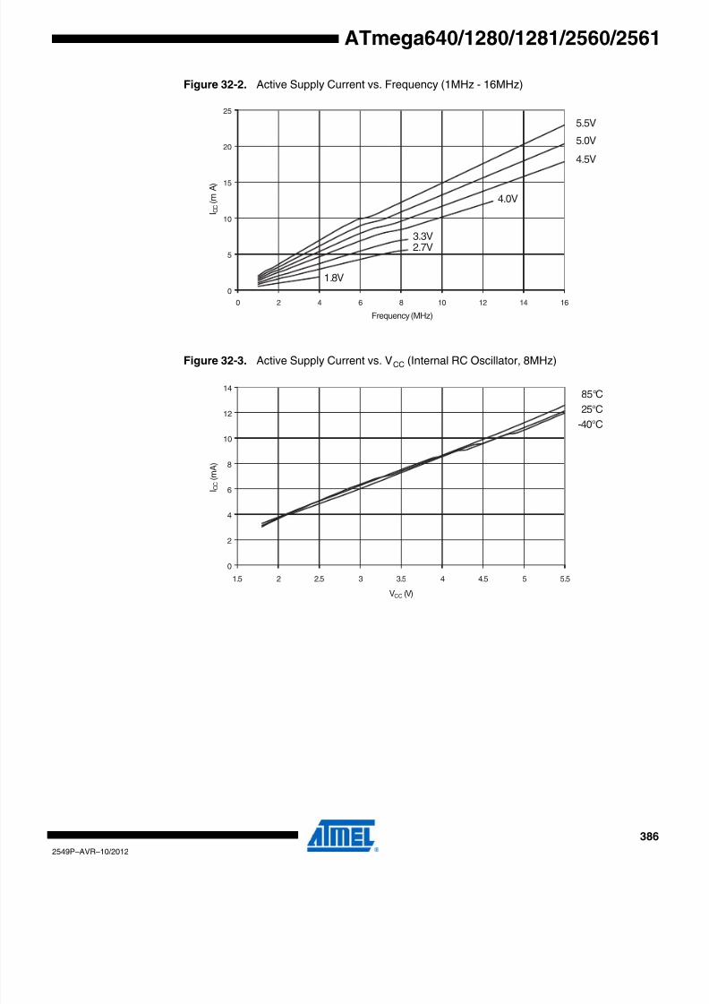
8/20/2019 At Mega 1281 Unlocked
http://slidepdf.com/reader/full/at-mega-1281-unlocked 386/446
386
2549P–AVR–10/2012
ATmega640/1280/1281/2560/2561
Figure 32-2. Active Supply Current vs. Frequency (1MHz - 16MHz)
Figure 32-3. Active Supply Current vs. VCC (Internal RC Oscillator, 8MHz)
5.5V
5.0V
4.5V
0
5
10
15
20
25
0 2 4 6 8 10 12 14 16
Frequency (MHz)
I C C ( m A )
4.0V
3.3V2.7V
1.8V
85°C
25°C
-40°C
0
2
4
6
8
10
12
14
1.5 2 2.5 3 3.5 4 4.5 5 5.5
VCC (V)
I C C ( m A )

8/20/2019 At Mega 1281 Unlocked
http://slidepdf.com/reader/full/at-mega-1281-unlocked 387/446
387
2549P–AVR–10/2012
ATmega640/1280/1281/2560/2561
Figure 32-4. Active Supply Current vs. VCC (Internal RC Oscillator, 1MHz)
Figure 32-5. Active Supply Current vs. VCC (Internal RC Oscillator, 128kHz)
85°C25°C
-40°C
0
0.5
1
1.5
2
2.5
1.5 2 2.5 3 3.5 4 4.5 5 5.5
VCC (V)
I C C ( m
A )
85°C
25°C
-40°C
0
0.1
0.2
0.3
0.4
0.5
0.6
0.7
1.5 2 2.5 3 3.5 4 4.5 5 5.5
VCC (V)
I C C ( m A )

8/20/2019 At Mega 1281 Unlocked
http://slidepdf.com/reader/full/at-mega-1281-unlocked 388/446
388
2549P–AVR–10/2012
ATmega640/1280/1281/2560/2561
32.2 Idle Supply Current
Figure 32-6. Idle Supply Current vs. Low Frequency (0.1MHz - 1.0MHz)
Figure 32-7. Idle Supply Current vs. Frequency (1MHz - 16MHz)
5.5V
5.0V
4.5V
4.0V
3.3V
2.7V
1.8V
0
0.1
0.2
0.3
0.4
0.5
0.6
0 0.1 0.2 0.3 0.4 0.5 0.6 0.7 0.8 0.9 1
Frequency (MHz)
I C C ( m A )
5.5V
5.0V
4.5V
0
1
2
3
4
5
6
7
8
0 2 4 6 8 10 12 14 16
Frequency (MHz)
I C C ( m A )
4.0V
3.3V2.7V
1.8V

8/20/2019 At Mega 1281 Unlocked
http://slidepdf.com/reader/full/at-mega-1281-unlocked 389/446
389
2549P–AVR–10/2012
ATmega640/1280/1281/2560/2561
Figure 32-8. Idle Supply Current vs. VCC (Internal RC Oscillator, 8MHz)
Figure 32-9. Idle Supply Current vs. VCC (Internal RC Oscillator, 1MHz)
85°C25°C
-40°C
0
0.5
1
1.5
2
2.5
3
3.5
1.5 2 2.5 3 3.5 4 4.5 5 5.5
VCC (V)
I C C ( m A )
85°C
25°C
-40°C
0
0.1
0.2
0.3
0.4
0.5
0.6
0.7
0.8
0.9
1.5 2 2.5 3 3.5 4 4.5 5 5.5
VCC (V)
I C C ( m A )

8/20/2019 At Mega 1281 Unlocked
http://slidepdf.com/reader/full/at-mega-1281-unlocked 390/446
390
2549P–AVR–10/2012
ATmega640/1280/1281/2560/2561
Figure 32-10. Idle Supply Current vs. VCC (Internal RC Oscillator, 128kHz)I
32.2.1 Supply Current of IO modules
The tables and formulas below can be used to calculate the additional current consumption fo
the different I/O modules in Active and Idle mode. The enabling or disabling of the I/O modules
are controlled by the Power Reduction Register. See “Power Reduction Register” on page 54 fo
details.
85°C
25°C
-40°C
0
0.05
0.1
0.15
0.2
0.25
0.3
1.5 2 2.5 3 3.5 4 4.5 5 5.5
VCC (V)
I C C ( m A )
Table 32-1. Additional Current Consumption for the different I/O modules (absolute values)
PRR bit Typical numbers
VCC = 2V, F = 1MHz VCC = 3V, F = 4MHz VCC = 5V, F = 8MHz
PRUSART3 8.0µA 51µA 220µA
PRUSART2 8.0µA 51µA 220µA
PRUSART1 8.0µA 51µA 220µA
PRUSART0 8.0µA 51µA 220µA
PRTWI 12µA 75µA 315µA
PRTIM5 6.0µA 39µA 150µA
PRTIM4 6.0µA 39µA 150µA
PRTIM3 6.0µA 39µA 150µA
PRTIM2 11µA 72µA 300µA
PRTIM1 6.0µA 39µA 150µA
PRTIM0 4.0µA 24µA 100µA
PRSPI 15µA 95µA 400µA
PRADC 12µA 75µA 315µA
8/20/2019 At Mega 1281 Unlocked
http://slidepdf.com/reader/full/at-mega-1281-unlocked 391/446
391
2549P–AVR–10/2012
ATmega640/1280/1281/2560/2561
It is possible to calculate the typical current consumption based on the numbers from Table 32-1
on page 390 for other VCC and frequency settings than listed in Table 32-2.
32.2.1.1 Example 1
Calculate the expected current consumption in idle mode with USART0, TIMER1, and TW
enabled at VCC = 2.0V and F = 1MHz. From Table 32-2, third column, we see that we need to
add 17% for the USART0, 24% for the TWI, and 10% for the TIMER1 module. Reading from Fig
ure 32-6 on page 388, we find that the idle current consumption is ~0.15mA at VCC = 2.0V and F
= 1MHz. The total current consumption in idle mode with USART0, TIMER1, and TWI enabled
gives:
Table 32-2. Additional Current Consumption (percentage) in Active and Idle mode
PRR bit
Additional Current consumption
compared to Active with external clock
Additional Current consumption
compared to Idle with external clock
PRUSART3 3.0% 17%
PRUSART2 3.0% 17%
PRUSART1 3.0% 17%
PRUSART0 3.0% 17%
PRTWI 4.4% 24%
PRTIM5 1.8% 10%
PRTIM4 1.8% 10%
PRTIM3 1.8% 10%
PRTIM2 4.3% 23%
PRTIM1 1.8% 10%
PRTIM0 1.5% 8.0%
PRSPI 3.3% 18%
PRADC 4.5% 24%
ICCtotal 0.15mA 1 0.17 0.24 0.10+ + +( )• 0.227mA≈ ≈

8/20/2019 At Mega 1281 Unlocked
http://slidepdf.com/reader/full/at-mega-1281-unlocked 392/446
392
2549P–AVR–10/2012
ATmega640/1280/1281/2560/2561
32.3 Power-down Supply Current
Figure 32-11. Power-down Supply Current vs. VCC (Watchdog Timer Disabled)
Figure 32-12. Power-down Supply Current vs. VCC (Watchdog Timer Enabled)
85°C
25°C
-40°C
0
0.5
1
1.5
2
2.5
3
3.5
4
1.5 2 2.5 3 3.5 4 4.5 5 5.5
VCC (V)
I C C ( µ A )
25°C
-40°C
0
2
4
6
8
10
12
1.5 2 2.5 3 3.5 4 4.5 5 5.5
VCC (V)
I C C ( µ A )
85°C

8/20/2019 At Mega 1281 Unlocked
http://slidepdf.com/reader/full/at-mega-1281-unlocked 393/446
393
2549P–AVR–10/2012
ATmega640/1280/1281/2560/2561
32.4 Power-save Supply Current
Figure 32-13. Power-save Supply Current vs. VCC (Watchdog Timer Disabled)
Figure 32-14. Power-save Supply Current vs. VCC (Watchdog Timer Enabled)
25°C
4
5
6
7
8
9
10
11
1.5 2 2.5 3 3.5 4 4.5 5 5.5
VCC
(V)
I C C ( µ A )
0
1
2
3
4
5
6
7
8
9
1.5 2 2.5 3 3.5 4 4.5 5 5.5
VCC (V)
I C C ( µ A )
25°C

8/20/2019 At Mega 1281 Unlocked
http://slidepdf.com/reader/full/at-mega-1281-unlocked 394/446
394
2549P–AVR–10/2012
ATmega640/1280/1281/2560/2561
32.5 Standby Supply Current
Figure 32-15. Standby Supply Current vs. VCC (Watchdog Timer Disabled)
32.6 Pin Pull-up
Figure 32-16. I/O Pin Pull-up Resistor Current vs. Input Voltage (VCC = 1.8V)
6MHz xtal
6MHz res
4MHz xtal 4MHz res
455kHz res
32kHz xtal
2MHz xtal
2MHz res
1MHz res
0
0.02
0.04
0.06
0.08
0.1
0.12
0.14
0.16
0.18
0.2
1.5 2 2.5 3 3.5 4 4.5 5 5.5
VCC (V)
I C C ( m A )
85°C25°C
-40°C0
10
20
30
40
50
60
0 0.2 0.4 0.6 0.8 1 1.2 1.4 1.6 1.8 2
VOP (V)
I O P ( µ A )
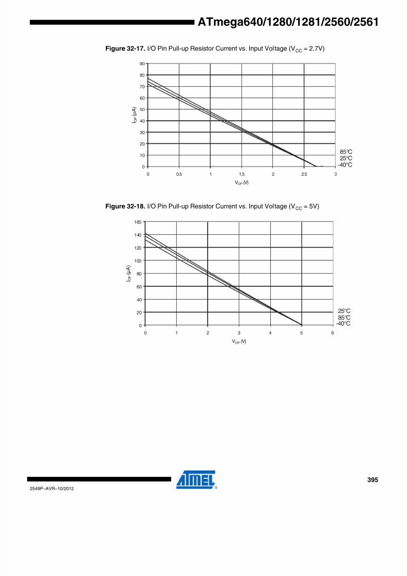
8/20/2019 At Mega 1281 Unlocked
http://slidepdf.com/reader/full/at-mega-1281-unlocked 395/446
395
2549P–AVR–10/2012
ATmega640/1280/1281/2560/2561
Figure 32-17. I/O Pin Pull-up Resistor Current vs. Input Voltage (VCC = 2.7V)
Figure 32-18. I/O Pin Pull-up Resistor Current vs. Input Voltage (VCC = 5V)
85°C25°C
-40°C0
10
20
30
40
50
60
70
80
90
0 0.5 1 1.5 2 2.5 3
VOP (V)
I O P ( µ A )
85°C25°C
-40°C0
20
40
60
80
100
120
140
160
0 1 2 3 4 5 6
VOP (V)
I O P ( µ A )

8/20/2019 At Mega 1281 Unlocked
http://slidepdf.com/reader/full/at-mega-1281-unlocked 396/446
396
2549P–AVR–10/2012
ATmega640/1280/1281/2560/2561
Figure 32-19. Reset Pull-up Resistor Current vs. Reset Pin Voltage (VCC = 1.8V)
Figure 32-20. Reset pull-up Resistor Current vs. Reset Pin Voltage (VCC = 2.7V)
85°C
25°C-40°C
0
5
10
15
20
25
30
35
40
0 0.2 0.4 0.6 0.8 1 1.2 1.4 1.6 1.8 2
VRESET (V)
I R E S E T
( µ A )
85°C
25°C-40°C
0
10
20
30
40
50
60
70
0 0.5 1 1.5 2 2.5 3
VRESET (V)
I R E S E T
( µ A )

8/20/2019 At Mega 1281 Unlocked
http://slidepdf.com/reader/full/at-mega-1281-unlocked 397/446
397
2549P–AVR–10/2012
ATmega640/1280/1281/2560/2561
Figure 32-21. Reset Pull-up Resistor Current vs. Reset Pin Voltage (VCC = 5V)
32.7 Pin Driver Strength
Figure 32-22. I/O Pin output Voltage vs.Sink Current (VCC = 3V)
85°C
25°C-40°C
0
20
40
60
80
100
120
0 1 2 3 4 5 6
VRESET (V)
I R E S E T ( µ A )
85°C
25°C
-40°C
0
0.1
0.2
0.3
0.4
0.5
0.6
0.7
0.8
0.9
1
0 5 10 15 20 25
IOL (mA)
V O L ( V )
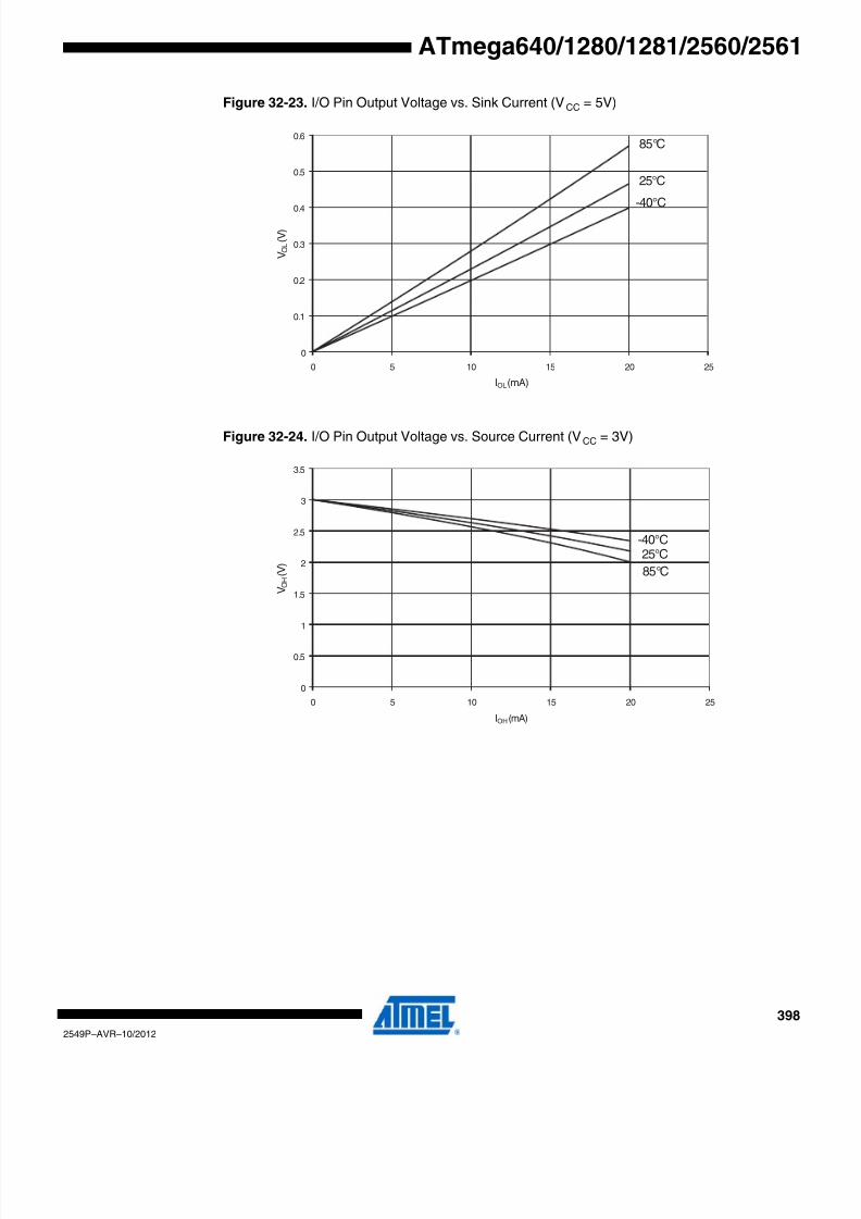
8/20/2019 At Mega 1281 Unlocked
http://slidepdf.com/reader/full/at-mega-1281-unlocked 398/446
398
2549P–AVR–10/2012
ATmega640/1280/1281/2560/2561
Figure 32-23. I/O Pin Output Voltage vs. Sink Current (VCC = 5V)
Figure 32-24. I/O Pin Output Voltage vs. Source Current (VCC = 3V)
25°C
-40°C
0
0.1
0.2
0.3
0.4
0.5
0.6
0 5 10 15 20 25
IOL (mA)
V O L ( V )
85°C
85°C
25°C-40°C
0
0.5
1
1.5
2
2.5
3
3.5
0 5 10 15 20 25
IOH (mA)
V O H ( V )

8/20/2019 At Mega 1281 Unlocked
http://slidepdf.com/reader/full/at-mega-1281-unlocked 399/446
399
2549P–AVR–10/2012
ATmega640/1280/1281/2560/2561
Figure 32-25. I/O Pin Output Voltage vs. Source Current (VCC = 5V)
32.8 Pin Threshold and Hysteresis
Figure 32-26. I/O Pin Input Threshold Voltage vs. VCC (VIH, IO Pin Read as “1“)
85°C
25°C
-40°C
4.3
4.4
4.5
4.6
4.7
4.8
4.9
5
5.1
0 5 10 15 20 25
IOH (mA)
V O H ( V )
85°C25°C
-40°C
0
0.5
1
1.5
2
2.5
3
3.5
1.5 2 2.5 3 3.5 4 4.5 5 5.5
VCC (V)
T h r e s
h o l d ( V )
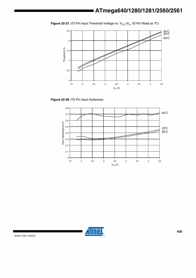
8/20/2019 At Mega 1281 Unlocked
http://slidepdf.com/reader/full/at-mega-1281-unlocked 400/446
400
2549P–AVR–10/2012
ATmega640/1280/1281/2560/2561
Figure 32-27. I/O Pin Input Threshold Voltage vs. VCC (VIL, IO Pin Read as “0“)
Figure 32-28. I/O Pin Input Hysteresis
85°C25°C
-40°C
0
0.5
1
1.5
2
2.5
1.5 2 2.5 3 3.5 4 4.5 5 5.5
VCC (V)
T h r e s h o l d ( V )
85°C
25°C
-40°C
0
0.1
0.2
0.3
0.4
0.5
0.6
0.7
0.8
1.5 2 2.5 3 3.5 4 4.5 5 5.5
VCC (V)
I n p
u t H y s t e r e s i s ( m V )

8/20/2019 At Mega 1281 Unlocked
http://slidepdf.com/reader/full/at-mega-1281-unlocked 401/446
401
2549P–AVR–10/2012
ATmega640/1280/1281/2560/2561
Figure 32-29. Reset Input Threshold Voltage vs. VCC (VIH, IO Pin Read as “1“)
Figure 32-30. Reset Input Threshold Voltage vs. VCC (VIL, IO Pin Read as “0“)
85°C25°C
-40°C
0
0.5
1
1.5
2
2.5
1.5 2 2.5 3 3.5 4 4.5 5 5.5
VCC (V)
T h r e s h o l d ( V )
85°C25°C
-40°C
0
0.5
1
1.5
2
2.5
1.5 2 2.5 3 3.5 4 4.5 5 5.5
VCC (V)
T h r e s h o l d ( V )

8/20/2019 At Mega 1281 Unlocked
http://slidepdf.com/reader/full/at-mega-1281-unlocked 402/446
402
2549P–AVR–10/2012
ATmega640/1280/1281/2560/2561
Figure 32-31. Reset Pin Input Hysteresis vs. VCC
32.9 BOD Threshold and Analog Comparator Offset
Figure 32-32. BOD Threshold vs. Temperature (BOD Level is 4.3V)
85°C25°C
-40°C
0
0.1
0.2
0.3
0.4
0.5
0.6
0.7
1.5 2 2.5 3 3.5 4 4.5 5 5.5
VCC (V)
I n p u t H y s t e r e s i s ( m V
)
Rising Vcc
Falling Vcc
4.2
4.25
4.3
4.35
4.4
-60 -40 -20 0 20 40 60 80 100
Temperature (°C)
T h r e s h o
l d (
V )
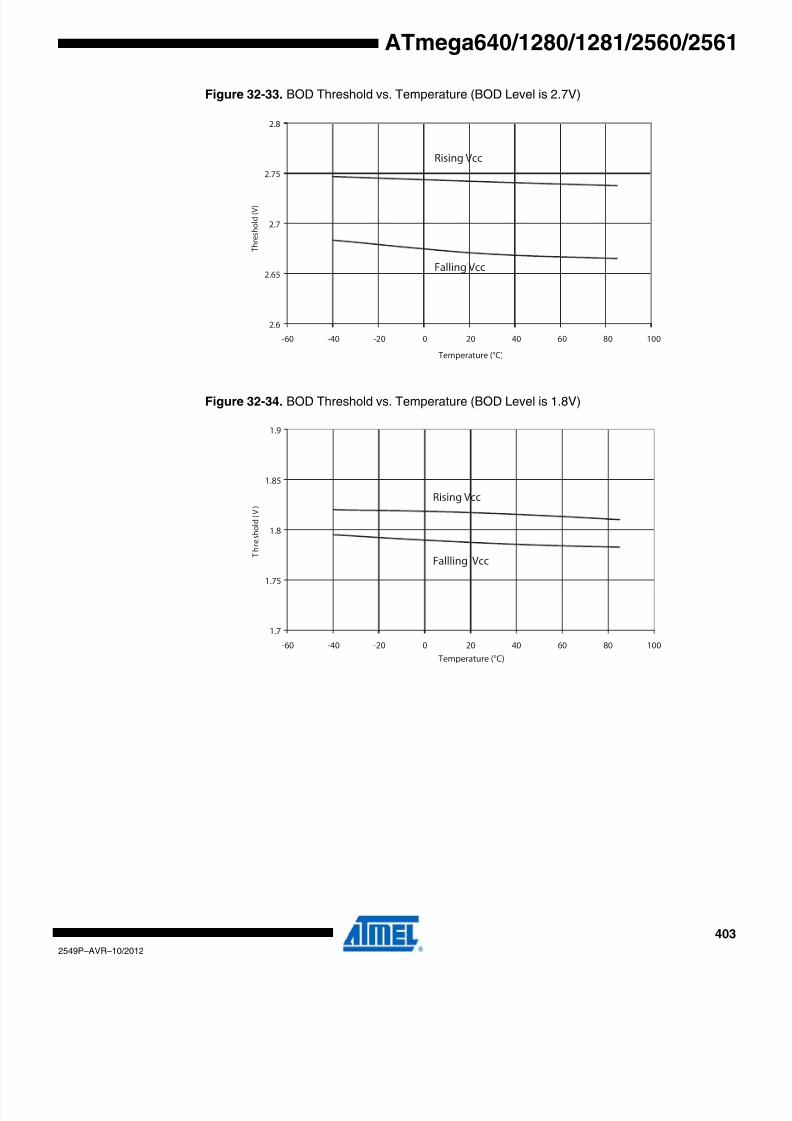
8/20/2019 At Mega 1281 Unlocked
http://slidepdf.com/reader/full/at-mega-1281-unlocked 403/446
403
2549P–AVR–10/2012
ATmega640/1280/1281/2560/2561
Figure 32-33. BOD Threshold vs. Temperature (BOD Level is 2.7V)
Figure 32-34. BOD Threshold vs. Temperature (BOD Level is 1.8V)
Rising Vcc
Falling Vcc
2.6
2.65
2.7
2.75
2.8
-60 -40 -20 0 20 40 60 80 100
Temperature (°C)
T h r e s h o l d
( V )
Rising Vcc
Fallling Vcc
1.7
1.75
1.8
1.85
1.9
-60 -40 -20 0 20 40 60 80 100
Temperature (°C)
T h r e s h o l d
( V
)

8/20/2019 At Mega 1281 Unlocked
http://slidepdf.com/reader/full/at-mega-1281-unlocked 404/446
404
2549P–AVR–10/2012
ATmega640/1280/1281/2560/2561
32.10 Internal Oscillator Speed
Figure 32-35. Watchdog Oscillator Frequency vs. VCC
Figure 32-36. Watchdog Oscillator Frequency vs. Temperature
85°C
25°C
-40°C
114
116
118
120
122
124
126
128
2 2.5 3 3.5 4 4.5 5 5.5
VCC (V)
F R C ( k H z )
5.5V
4.0V3.3V2.7V2.1V
114
116
118
120
122
124
126
128
-60 -40 -20 0 20 40 60 80 100
Temperature (°C)
F R C ( k
H z )

8/20/2019 At Mega 1281 Unlocked
http://slidepdf.com/reader/full/at-mega-1281-unlocked 405/446
405
2549P–AVR–10/2012
ATmega640/1280/1281/2560/2561
Figure 32-37. Calibrated 8MHz RC Oscillator Frequency vs. VCC
Figure 32-38. Calibrated 8MHz RC Oscillator Frequency vs. Temperature
85°C
25°C
-40°C
7.6
7.7
7.8
7.9
8
8.1
8.2
8.3
1.5 2 2.5 3 3.5 4 4.5 5 5.5
VCC (V)
F R C ( M H z )
5.0V
3.0V
7.9
8
8.1
8.2
8.3
8.4
8.5
-60 -40 -20 0 20 40 60 80 100
Temperature (°C)
F R C ( M H z )

8/20/2019 At Mega 1281 Unlocked
http://slidepdf.com/reader/full/at-mega-1281-unlocked 406/446
406
2549P–AVR–10/2012
ATmega640/1280/1281/2560/2561
Figure 32-39. Calibrated 8MHz RC Oscillator Frequency vs. Osccal Value
32.11 Current Consumption of Peripheral Units
Figure 32-40. Brownout Detector Current vs. VCC
85°C25°C
-40°C
0
2
4
6
8
10
12
14
16
0 16 32 48 64 80 96 112 128 144 160 176 192 208 224 240 256
OSCCAL (X1)
F R C ( M H z )
85°C
25°C
-40°C
0
5
10
15
20
25
30
1.5 2 2.5 3 3.5 4 4.5 5 5.5
VCC (V)
I C C ( µ A )

8/20/2019 At Mega 1281 Unlocked
http://slidepdf.com/reader/full/at-mega-1281-unlocked 407/446
407
2549P–AVR–10/2012
ATmega640/1280/1281/2560/2561
Figure 32-41. ADC Current vs. VCC (AREF = AVCC)
Figure 32-42. AREF External Reference Current vs. VCC
85°C25°C
-40°C
0
50
100
150
200
250
300
350
1.5 2 2.5 3 3.5 4 4.5 5 5.5
VCC (V)
I C C ( µ A )
85°C25°C
-40°C
0
50
100
150
200
250
1.5 2 2.5 3 3.5 4 4.5 5 5.5
VCC (V)
I C C ( µ A )

8/20/2019 At Mega 1281 Unlocked
http://slidepdf.com/reader/full/at-mega-1281-unlocked 408/446
408
2549P–AVR–10/2012
ATmega640/1280/1281/2560/2561
Figure 32-43. Watchdog Timer Current vs. VCC
Figure 32-44. Analog Comparator Current vs. VCC
85°C25°C
-40°C
0
1
2
3
4
5
6
7
8
9
1.5 2 2.5 3 3.5 4 4.5 5 5.5
VCC (V)
I C C ( µ A )
85°C25°C
-40°C
0
10
20
30
40
50
60
70
80
90
100
1.5 2 2.5 3 3.5 4 4.5 5 5.5
VCC (V)
I C C ( µ A )

8/20/2019 At Mega 1281 Unlocked
http://slidepdf.com/reader/full/at-mega-1281-unlocked 409/446
409
2549P–AVR–10/2012
ATmega640/1280/1281/2560/2561
Figure 32-45. Programming Current vs. VCC
32.12 Current Consumption in Reset and Reset Pulsewidth
Figure 32-46. Reset Supply Current vs VCC (0.1MHz - 1.0MHz, Excluding Current Through TheReset Pull-up)
85°C
25°C
-40°C
0
2
4
6
8
10
12
14
16
1.5 2 2.5 3 3.5 4 4.5 5 5.5
VCC (V)
I C C ( m A )
5.5V
5.0V
4.5V
4.0V
3.3V
2.7V
1.8V
0
0.05
0.1
0.15
0.2
0.25
0.3
0.35
0 0.1 0.2 0.3 0.4 0.5 0.6 0.7 0.8 0.9 1
Frequency (MHz)
I C C ( m A
)
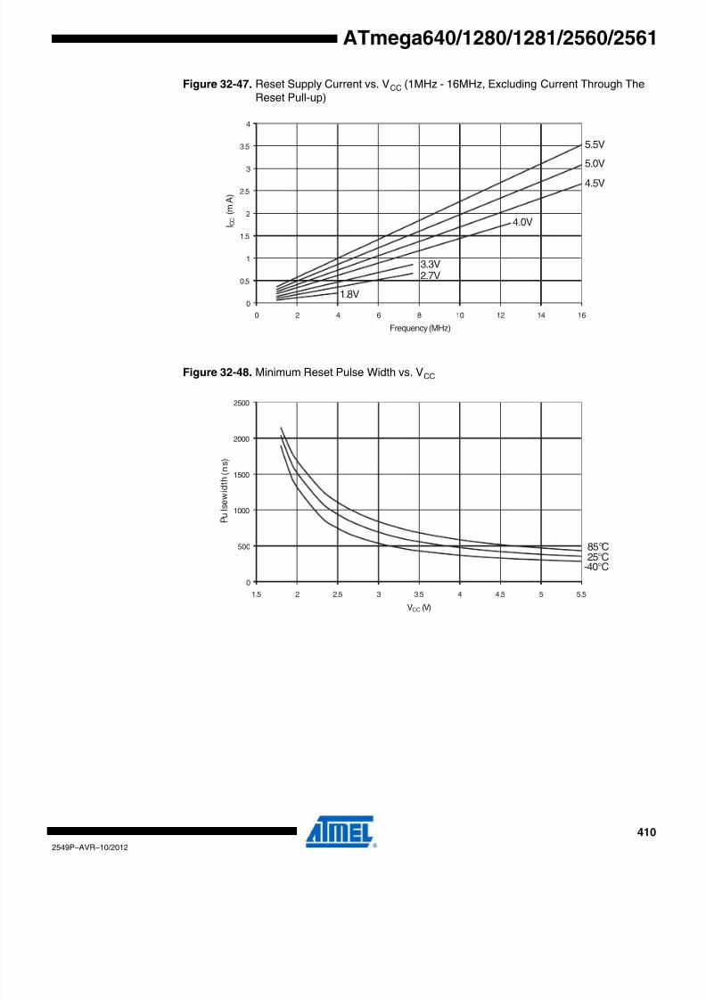
8/20/2019 At Mega 1281 Unlocked
http://slidepdf.com/reader/full/at-mega-1281-unlocked 410/446
410
2549P–AVR–10/2012
ATmega640/1280/1281/2560/2561
Figure 32-47. Reset Supply Current vs. VCC (1MHz - 16MHz, Excluding Current Through TheReset Pull-up)
Figure 32-48. Minimum Reset Pulse Width vs. VCC
5.5V
5.0V
4.5V
0
0.5
1
1.5
2
2.5
3
3.5
4
0 2 4 6 8 10 12 14 16
Frequency (MHz)
I C C
( m A )
4.0V
3.3V2.7V
1.8V
85°C25°C
-40°C
0
500
1000
1500
2000
2500
1.5 2 2.5 3 3.5 4 4.5 5 5.5
VCC (V)
P u l s e w i d t h ( n s )

8/20/2019 At Mega 1281 Unlocked
http://slidepdf.com/reader/full/at-mega-1281-unlocked 411/446
411
2549P–AVR–10/2012
ATmega640/1280/1281/2560/2561
33. Register SummaryAddress Name Bit 7 Bit 6 Bit 5 Bit 4 Bit 3 Bit 2 Bit 1 Bit 0 Page
(0x1FF) Reserved - - - - - - - -
... Reserved - - - - - - - -
(0x13F) Reserved
(0x13E) Reserved
(0x13D) Reserved
(0x13C) Reserved(0x13B) Reserved
(0x13A) Reserved
(0x139) Reserved
(0x138) Reserved
(0x137) Reserved
(0x136) UDR3 USART3 I/O Data Register 222
(0x135) UBRR3H - - - - USART3 Baud Rate Register High Byte 227
(0x134) UBRR3L USART3 Baud Rate Register Low Byte 227
(0x133) Reserved - - - - - - - -
(0x132) UCSR3C UMSEL31 UMSEL30 UPM31 UPM30 USBS3 UCSZ31 UCSZ30 UCPOL3 239
(0x131) UCSR3B RXCIE3 TXCIE3 UDRIE3 RXEN3 TXEN3 UCSZ32 RXB83 TXB83 238
(0x130) UCSR3A RXC3 TXC3 UDRE3 FE3 DOR3 UPE3 U2X3 MPCM3 238
(0x12F) Reserved - - - - - - - -
(0x12E) Reserved - - - - - - - -
(0x12D) OCR5CH Timer/Counter5 - Output Compare Register C High Byte 165
(0x12C) OCR5CL Timer/Counter5 - Output Compare Register C Low Byte 165(0x12B) OCR5BH Timer/Counter5 - Output Compare Register B High Byte 165
(0x12A) OCR5BL Timer/Counter5 - Output Compare Register B Low Byte 165
(0x129) OCR5AH Timer/Counter5 - Output Compare Register A High Byte 164
(0x128) OCR5AL Timer/Counter5 - Output Compare Register A Low Byte 164
(0x127) ICR5H Timer/Counter5 - Input Capture Register High Byte 165
(0x126) ICR5L Timer/Counter5 - Input Capture Register Low Byte 165
(0x125) TCNT5H Timer/Counter5 - Counter Register High Byte 163
(0x124) TCNT5L Timer/Counter5 - Counter Register Low Byte 163
(0x123) Reserved - - - - - - - -
(0x122) TCCR5C FOC5A FOC5B FOC5C - - - - - 162
(0x121) TCCR5B ICNC5 ICES5 - WGM53 WGM52 CS52 CS51 CS50 160
(0x120) TCCR5A COM5A1 COM5A0 COM5B1 COM5B0 COM5C1 COM5C0 WGM51 WGM50 158
(0x11F) Reserved - - - - - - - -
(0x11E) Reserved - - - - - - - -
(0x11D) Reserved - - - - - - - -
(0x11C) Reserved - - - - - - - -(0x11B) Reserved - - - - - - - -
(0x11A) Reserved - - - - - - - -
(0x119) Reserved - - - - - - - -
(0x118) Reserved - - - - - - - -
(0x117) Reserved - - - - - - - -
(0x116) Reserved - - - - - - - -
(0x115) Reserved - - - - - - - -
(0x114) Reserved - - - - - - - -
(0x113) Reserved - - - - - - - -
(0x112) Reserved - - - - - - - -
(0x111) Reserved - - - - - - - -
(0x110) Reserved - - - - - - - -
(0x10F) Reserved - - - - - - - -
(0x10E) Reserved - - - - - - - -
(0x10D) Reserved - - - - - - - -
(0x10C) Reserved - - - - - - - -(0x10B) PORTL PORTL7 PORTL6 PORTL5 PORTL4 PORTL3 PORTL2 PORTL1 PORTL0 104
(0x10A) DDRL DDL7 DDL6 DDL5 DDL4 DDL3 DDL2 DDL1 DDL0 104
(0x109) PINL PINL7 PINL6 PINL5 PINL4 PINL3 PINL2 PINL1 PINL0 104
(0x108) PORTK PORTK7 PORTK6 PORTK5 PORTK4 PORTK3 PORTK2 PORTK1 PORTK0 103
(0x107) DDRK DDK7 DDK6 DDK5 DDK4 DDK3 DDK2 DDK1 DDK0 103
(0x106) PINK PINK7 PINK6 PINK5 PINK4 PINK3 PINK2 PINK1 PINK0 103
(0x105) PORTJ PORTJ7 PORTJ6 PORTJ5 PORTJ4 PORTJ3 PORTJ2 PORTJ1 PORTJ0 103
(0x104) DDRJ DDJ7 DDJ6 DDJ5 DDJ4 DDJ3 DDJ2 DDJ1 DDJ0 103
(0x103) PINJ PINJ7 PINJ6 PINJ5 PINJ4 PINJ3 PINJ2 PINJ1 PINJ0 103
(0x102) PORTH PORTH7 PORTH6 PORTH5 PORTH4 PORTH3 PORTH2 PORTH1 PORTH0 102
(0x101) DDRH DDH7 DDH6 DDH5 DDH4 DDH3 DDH2 DDH1 DDH0 103

8/20/2019 At Mega 1281 Unlocked
http://slidepdf.com/reader/full/at-mega-1281-unlocked 412/446
412
2549P–AVR–10/2012
ATmega640/1280/1281/2560/2561
(0x100) PINH PINH7 PINH6 PINH5 PINH4 PINH3 PINH2 PINH1 PINH0 103
(0xFF) Reserved - - - - - - - -
(0xFE) Reserved - - - - - - - -
(0xFD) Reserved - - - - - - - -
(0xFC) Reserved - - - - - - - -
(0xFB) Reserved - - - - - - - -
(0xFA) Reserved - - - - - - - -
(0xF9) Reserved - - - - - - - -
(0xF8) Reserved - - - - - - - -
(0xF7) Reserved - - - - - - - -
(0xF6) Reserved - - - - - - - -
(0xF5) Reserved - - - - - - - -
(0xF4) Reserved - - - - - - - -
(0xF3) Reserved - - - - - - - -
(0xF2) Reserved - - - - - - - -
(0xF1) Reserved - - - - - - - -
(0xF0) Reserved - - - - - - - -
(0xEF) Reserved - - - - - - - -
(0xEE) Reserved - - - - - - - -
(0xED) Reserved - - - - - - - -
(0xEC) Reserved - - - - - - - -
(0xEB) Reserved - - - - - - -
(0xEA) Reserved - - - - - - - -
(0xE9) Reserved - - - - - - - -
(0xE8) Reserved - - - - - - - -
(0xE7) Reserved - - - - - - -
(0xE6) Reserved - - - - - - - -
(0xE5) Reserved - - - - - - - -
(0xE4) Reserved - - - - - - - -
(0xE3) Reserved - - - - - - -
(0xE2) Reserved - - - - - - - -
(0xE1) Reserved - - - - - - -
(0xE0) Reserved - - - - - - -
(0xDF) Reserved - - - - - - - -
(0xDE) Reserved - - - - - - - -
(0xDD) Reserved - - - - - - -
(0xDC) Reserved - - - - - - - -
(0xDB) Reserved - - - - - - - -
(0xDA) Reserved - - - - - - - -
(0xD9) Reserved - - - - - - -
(0xD8) Reserved - - - - - - - -
(0xD7) Reserved - - - - - - - -
(0xD6) UDR2 USART2 I/O Data Register 222
(0xD5) UBRR2H - - - - USART2 Baud Rate Register High Byte 227
(0xD4) UBRR2L USART2 Baud Rate Register Low Byte 227
(0xD3) Reserved - - - - - - - -
(0xD2) UCSR2C UMSEL21 UMSEL20 UPM21 UPM20 USBS2 UCSZ21 UCSZ20 UCPOL2 239
(0xD1) UCSR2B RXCIE2 TXCIE2 UDRIE2 RXEN2 TXEN2 UCSZ22 RXB82 TXB82 238
(0xD0) UCSR2A RXC2 TXC2 UDRE2 FE2 DOR2 UPE2 U2X2 MPCM2 238
(0xCF) Reserved - - - - - - - -
(0xCE) UDR1 USART1 I/O Data Register 222
(0xCD) UBRR1H - - - - USART1 Baud Rate Register High Byte 227
(0xCC) UBRR1L USART1 Baud Rate Register Low Byte 227
(0xCB) Reserved - - - - - - - -
(0xCA) UCSR1C UMSEL11 UMSEL10 UPM11 UPM10 USBS1 UCSZ11 UCSZ10 UCPOL1 239
(0xC9) UCSR1B RXCIE1 TXCIE1 UDRIE1 RXEN1 TXEN1 UCSZ12 RXB81 TXB81 238
(0xC8) UCSR1A RXC1 TXC1 UDRE1 FE1 DOR1 UPE1 U2X1 MPCM1 238
(0xC7) Reserved - - - - - - - -
(0xC6) UDR0 USART0 I/O Data Register 222
(0xC5) UBRR0H - - - - USART0 Baud Rate Register High Byte 227
(0xC4) UBRR0L USART0 Baud Rate Register Low Byte 227
(0xC3) Reserved - - - - - - - -
(0xC2) UCSR0C UMSEL01 UMSEL00 UPM01 UPM00 USBS0 UCSZ01 UCSZ00 UCPOL0 239
(0xC1) UCSR0B RXCIE0 TXCIE0 UDRIE0 RXEN0 TXEN0 UCSZ02 RXB80 TXB80 238
(0xC0) UCSR0A RXC0 TXC0 UDRE0 FE0 DOR0 UPE0 U2X0 MPCM0 238
(0xBF) Reserved - - - - - - - -
Address Name Bit 7 Bit 6 Bit 5 Bit 4 Bit 3 Bit 2 Bit 1 Bit 0 Page

8/20/2019 At Mega 1281 Unlocked
http://slidepdf.com/reader/full/at-mega-1281-unlocked 413/446
413
2549P–AVR–10/2012
ATmega640/1280/1281/2560/2561
(0xBE) Reserved - - - - - - - -
(0xBD) TWAMR TWAM6 TWAM5 TWAM4 TWAM3 TWAM2 TWAM1 TWAM0 - 269
(0xBC) TWCR TWINT TWEA TWSTA TWSTO TWWC TWEN - TWIE 266
(0xBB) TWDR 2-wire Serial Interface Data Register 268
(0xBA) TWAR TWA6 TWA5 TWA4 TWA3 TWA2 TWA1 TWA0 TWGCE 269
(0xB9) TWSR TWS7 TWS6 TWS5 TWS4 TWS3 - TWPS1 TWPS0 268
(0xB8) TWBR 2-wire Serial Interface Bit Rate Register 266
(0xB7) Reserved - - - - - - - -
(0xB6) ASSR - EXCLK AS2 TCN2UB OCR2AUB OCR2BUB TCR2AUB TCR2BUB 184
(0xB5) Reserved - - - - - - - -
(0xB4) OCR2B Timer/Counter2 Output Compare Register B 191
(0xB3) OCR2A Timer/Counter2 Output Compare Register A 191
(0xB2) TCNT2 Timer/Counter2 (8 Bit) 191
(0xB1) TCCR2B FOC2A FOC2B - - WGM22 CS22 CS21 CS20 190
(0xB0) TCCR2A COM2A1 COM2A0 COM2B1 COM2B0 - - WGM21 WGM20 191
(0xAF) Reserved - - - - - - - -
(0xAE) Reserved - - - - - - - -
(0xAD) OCR4CH Timer/Counter4 - Output Compare Register C High Byte 164
(0xAC) OCR4CL Timer/Counter4 - Output Compare Register C Low Byte 164
(0xAB) OCR4BH Timer/Counter4 - Output Compare Register B High Byte 164
(0xAA) OCR4BL Timer/Counter4 - Output Compare Register B Low Byte 164
(0xA9) OCR4AH Timer/Counter4 - Output Compare Register A High Byte 164
(0xA8) OCR4AL Timer/Counter4 - Output Compare Register A Low Byte 164
(0xA7) ICR4H Timer/Counter4 - Input Capture Register High Byte 165
(0xA6) ICR4L Timer/Counter4 - Input Capture Register Low Byte 165
(0xA5) TCNT4H Timer/Counter4 - Counter Register High Byte 163
(0xA4) TCNT4L Timer/Counter4 - Counter Register Low Byte 163
(0xA3) Reserved - - - - - - - -
(0xA2) TCCR4C FOC4A FOC4B FOC4C - - - - - 162
(0xA1) TCCR4B ICNC4 ICES4 - WGM43 WGM42 CS42 CS41 CS40 160
(0xA0) TCCR4A COM4A1 COM4A0 COM4B1 COM4B0 COM4C1 COM4C0 WGM41 WGM40 158
(0x9F) Reserved - - - - - - - -
(0x9E) Reserved - - - - - - - -
(0x9D) OCR3CH Timer/Counter3 - Output Compare Register C High Byte 164
(0x9C) OCR3CL Timer/Counter3 - Output Compare Register C Low Byte 164
(0x9B) OCR3BH Timer/Counter3 - Output Compare Register B High Byte 164
(0x9A) OCR3BL Timer/Counter3 - Output Compare Register B Low Byte 164
(0x99) OCR3AH Timer/Counter3 - Output Compare Register A High Byte 163
(0x98) OCR3AL Timer/Counter3 - Output Compare Register A Low Byte 163
(0x97) ICR3H Timer/Counter3 - Input Capture Register High Byte 165
(0x96) ICR3L Timer/Counter3 - Input Capture Register Low Byte 165
(0x95) TCNT3H Timer/Counter3 - Counter Register High Byte 162
(0x94) TCNT3L Timer/Counter3 - Counter Register Low Byte 162
(0x93) Reserved - - - - - - - -
(0x92) TCCR3C FOC3A FOC3B FOC3C - - - - - 162
(0x91) TCCR3B ICNC3 ICES3 - WGM33 WGM32 CS32 CS31 CS30 160
(0x90) TCCR3A COM3A1 COM3A0 COM3B1 COM3B0 COM3C1 COM3C0 WGM31 WGM30 158
(0x8F) Reserved - - - - - - - -
(0x8E) Reserved - - - - - - - -
(0x8D) OCR1CH Timer/Counter1 - Output Compare Register C High Byte 163
(0x8C) OCR1CL Timer/Counter1 - Output Compare Register C Low Byte 163
(0x8B) OCR1BH Timer/Counter1 - Output Compare Register B High Byte 163
(0x8A) OCR1BL Timer/Counter1 - Output Compare Register B Low Byte 163
(0x89) OCR1AH Timer/Counter1 - Output Compare Register A High Byte 163
(0x88) OCR1AL Timer/Counter1 - Output Compare Register A Low Byte 163
(0x87) ICR1H Timer/Counter1 - Input Capture Register High Byte 165
(0x86) ICR1L Timer/Counter1 - Input Capture Register Low Byte 165
(0x85) TCNT1H Timer/Counter1 - Counter Register High Byte 162
(0x84) TCNT1L Timer/Counter1 - Counter Register Low Byte 162
(0x83) Reserved - - - - - - - -
(0x82) TCCR1C FOC1A FOC1B FOC1C - - - - - 161
(0x81) TCCR1B ICNC1 ICES1 - WGM13 WGM12 CS12 CS11 CS10 160
(0x80) TCCR1A COM1A1 COM1A0 COM1B1 COM1B0 COM1C1 COM1C0 WGM11 WGM10 158
(0x7F) DIDR1 - - - - - - AIN1D AIN0D 274
(0x7E) DIDR0 ADC7D ADC6D ADC5D ADC4D ADC3D ADC2D ADC1D ADC0D 295
(0x7D) DIDR2 ADC15D ADC14D ADC13D ADC12D ADC11D ADC10D ADC9D ADC8D 295
Address Name Bit 7 Bit 6 Bit 5 Bit 4 Bit 3 Bit 2 Bit 1 Bit 0 Page
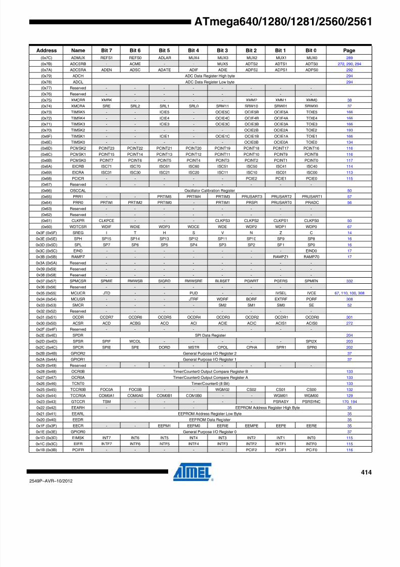
8/20/2019 At Mega 1281 Unlocked
http://slidepdf.com/reader/full/at-mega-1281-unlocked 414/446
414
2549P–AVR–10/2012
ATmega640/1280/1281/2560/2561
(0x7C) ADMUX REFS1 REFS0 ADLAR MUX4 MUX3 MUX2 MUX1 MUX0 289
(0x7B) ADCSRB - ACME - - MUX5 ADTS2 ADTS1 ADTS0 272, 290, 294
(0x7A) ADCSRA ADEN ADSC ADATE ADIF ADIE ADPS2 ADPS1 ADPS0 292
(0x79) ADCH ADC Data Register High byte 294
(0x78) ADCL ADC Data Register Low byte 294
(0x77) Reserved - - - - - - - -
(0x76) Reserved - - - - - - - -
(0x75) XMCRB XMBK - - - - XMM2 XMM1 XMM0 38
(0x74) XMCRA SRE SRL2 SRL1 SRL0 SRW11 SRW10 SRW01 SRW00 37
(0x73) TIMSK5 - - ICIE5 - OCIE5C OCIE5B OCIE5A TOIE5 166
(0x72) TIMSK4 - - ICIE4 - OCIE4C OCIE4B OCIE4A TOIE4 166
(0x71) TIMSK3 - - ICIE3 - OCIE3C OCIE3B OCIE3A TOIE3 166
(0x70) TIMSK2 - - - - - OCIE2B OCIE2A TOIE2 193
(0x6F) TIMSK1 - - ICIE1 - OCIE1C OCIE1B OCIE1A TOIE1 166
(0x6E) TIMSK0 - - - - - OCIE0B OCIE0A TOIE0 134
(0x6D) PCMSK2 PCINT23 PCINT22 PCINT21 PCINT20 PCINT19 PCINT18 PCINT17 PCINT16 116
(0x6C) PCMSK1 PCINT15 PCINT14 PCINT13 PCINT12 PCINT11 PCINT10 PCINT9 PCINT8 116
(0x6B) PCMSK0 PCINT7 PCINT6 PCINT5 PCINT4 PCINT3 PCINT2 PCINT1 PCINT0 117
(0x6A) EICRB ISC71 ISC70 ISC61 ISC60 ISC51 ISC50 ISC41 ISC40 114
(0x69) EICRA ISC31 ISC30 ISC21 ISC20 ISC11 ISC10 ISC01 ISC00 113
(0x68) PCICR - - - - - PCIE2 PCIE1 PCIE0 115
(0x67) Reserved - - - - - - - -
(0x66) OSCCAL Oscillator Calibration Register 50
(0x65) PRR1 - - PRTIM5 PRTIM4 PRTIM3 PRUSART3 PRUSART2 PRUSART1 57
(0x64) PRR0 PRTWI PRTIM2 PRTIM0 - PRTIM1 PRSPI PRUSART0 PRADC 56
(0x63) Reserved - - - - - - - -
(0x62) Reserved - - - - - - - -
(0x61) CLKPR CLKPCE - - - CLKPS3 CLKPS2 CLKPS1 CLKPS0 50
(0x60) WDTCSR WDIF WDIE WDP3 WDCE WDE WDP2 WDP1 WDP0 67
0x3F (0x5F) SREG I T H S V N Z C 14
0x3E (0x5E) SPH SP15 SP14 SP13 SP12 SP11 SP10 SP9 SP8 16
0x3D (0x5D) SPL SP7 SP6 SP5 SP4 SP3 SP2 SP1 SP0 16
0x3C (0x5C) EIND - - - - - - - EIND0 17
0x3B (0x5B) RAMPZ - - - - - - RAMPZ1 RAMPZ0 17
0x3A (0x5A) Reserved - - - - - - - -
0x39 (0x59) Reserved - - - - - - - -
0x38 (0x58) Reserved - - - - - - - -
0x37 (0x57) SPMCSR SPMIE RWWSB SIGRD RWWSRE BLBSET PGWRT PGERS SPMEN 332
0x36 (0x56) Reserved - - - - - - - -
0x35 (0x55) MCUCR JTD - - PUD - - IVSEL IVCE 67, 110, 100, 308
0x34 (0x54) MCUSR - - - JTRF WDRF BORF EXTRF PORF 308
0x33 (0x53) SMCR - - - - SM2 SM1 SM0 SE 52
0x32 (0x52) Reserved - - - - - - - -
0x31 (0x51) OCDR OCDR7 OCDR6 OCDR5 OCDR4 OCDR3 OCDR2 OCDR1 OCDR0 301
0x30 (0x50) ACSR ACD ACBG ACO ACI ACIE ACIC ACIS1 ACIS0 272
0x2F (0x4F) Reserved - - - - - - - -
0x2E (0x4E) SPDR SPI Data Register 204
0x2D (0x4D) SPSR SPIF WCOL - - - - - SPI2X 203
0x2C (0x4C) SPCR SPIE SPE DORD MSTR CPOL CPHA SPR1 SPR0 202
0x2B (0x4B) GPIOR2 General Purpose I/O Register 2 37
0x2A (0x4A) GPIOR1 General Purpose I/O Register 1 37
0x29 (0x49) Reserved - - - - - - - -
0x28 (0x48) OCR0B Timer/Counter0 Output Compare Register B 133
0x27 (0x47) OCR0A Timer/Counter0 Output Compare Register A 133
0x26 (0x46) TCNT0 Timer/Counter0 (8 Bit) 133
0x25 (0x45) TCCR0B FOC0A FOC0B - - WGM02 CS02 CS01 CS00 132
0x24 (0x44) TCCR0A COM0A1 COM0A0 COM0B1 COM0B0 - - WGM01 WGM00 129
0x23 (0x43) GTCCR TSM - - - - - PSRASY PSRSYNC 170, 194
0x22 (0x42) EEARH - - - - EEPROM Address Register High Byte 35
0x21 (0x41) EEARL EEPROM Address Register Low Byte 35
0x20 (0x40) EEDR EEPROM Data Register 35
0x1F (0x3F) EECR - - EEPM1 EEPM0 EERIE EEMPE EEPE EERE 35
0x1E (0x3E) GPIOR0 General Purpose I/O Register 0 37
0x1D (0x3D) EIMSK INT7 INT6 INT5 INT4 INT3 INT2 INT1 INT0 115
0x1C (0x3C) EIFR INTF7 INTF6 INTF5 INTF4 INTF3 INTF2 INTF1 INTF0 115
0x1B (0x3B) PCIFR - - - - - PCIF2 PCIF1 PCIF0 116
Address Name Bit 7 Bit 6 Bit 5 Bit 4 Bit 3 Bit 2 Bit 1 Bit 0 Page

8/20/2019 At Mega 1281 Unlocked
http://slidepdf.com/reader/full/at-mega-1281-unlocked 415/446
415
2549P–AVR–10/2012
ATmega640/1280/1281/2560/2561
Notes: 1. For compatibility with future devices, reserved bits should be written to zero if accessed. Reserved I/O memory addressesshould never be written.
2. I/O registers within the address range $00 - $1F are directly bit-accessible using the SBI and CBI instructions. In these reg-isters, the value of single bits can be checked by using the SBIS and SBIC instructions.
3. Some of the status flags are cleared by writing a logical one to them. Note that the CBI and SBI instructions will operate onall bits in the I/O register, writing a one back into any flag read as set, thus clearing the flag. The CBI and SBI instructionswork with registers 0x00 to 0x1F only.
4. When using the I/O specific commands IN and OUT, the I/O addresses $00 - $3F must be used. When addressing I/O registers as data space using LD and ST instructions, $20 must be added to these addresses. The
ATmega640/1280/1281/2560/2561 is a complex microcontroller with more peripheral units than can be supported within the64 location reserved in Opcode for the IN and OUT instructions. For the Extended I/O space from $60 - $1FF in SRAM, onlythe ST/STS/STD and LD/LDS/LDD instructions can be used.
0x1A (0x3A) TIFR5 - - ICF5 - OCF5C OCF5B OCF5A TOV5 166
0x19 (0x39) TIFR4 - - ICF4 - OCF4C OCF4B OCF4A TOV4 167
0x18 (0x38) TIFR3 - - ICF3 - OCF3C OCF3B OCF3A TOV3 167
0x17 (0x37) TIFR2 - - - - - OCF2B OCF2A TOV2 193
0x16 (0x36) TIFR1 - - ICF1 - OCF1C OCF1B OCF1A TOV1 167
0x15 (0x35) TIFR0 - - - - - OCF0B OCF0A TOV0 134
0x14 (0x34) PORTG - - PORTG5 PORTG4 PORTG3 PORTG2 PORTG1 PORTG0 102
0x13 (0x33) DDRG - - DDG5 DDG4 DDG3 DDG2 DDG1 DDG0 102
0x12 (0x32) PING - - PING5 PING4 PING3 PING2 PING1 PING0 102
0x11 (0x31) PORTF PORTF7 PORTF6 PORTF5 PORTF4 PORTF3 PORTF2 PORTF1 PORTF0 101
0x10 (0x30) DDRF DDF7 DDF6 DDF5 DDF4 DDF3 DDF2 DDF1 DDF0 102
0x0F (0x2F) PINF PINF7 PINF6 PINF5 PINF4 PINF3 PINF2 PINF1 PINF0 102
0x0E (0x2E) PORTE PORTE7 PORTE6 PORTE5 PORTE4 PORTE3 PORTE2 PORTE1 PORTE0 101
0x0D (0x2D) DDRE DDE7 DDE6 DDE5 DDE4 DDE3 DDE2 DDE1 DDE0 101
0x0C (0x2C) PINE PINE7 PINE6 PINE5 PINE4 PINE3 PINE2 PINE1 PINE0 102
0x0B (0x2B) PORTD PORTD7 PORTD6 PORTD5 PORTD4 PORTD3 PORTD2 PORTD1 PORTD0 101
0x0A (0x2A) DDRD DDD7 DDD6 DDD5 DDD4 DDD3 DDD2 DDD1 DDD0 101
0x09 (0x29) PIND PIND7 PIND6 PIND5 PIND4 PIND3 PIND2 PIND1 PIND0 101
0x08 (0x28) PORTC PORTC7 PORTC6 PORTC5 PORTC4 PORTC3 PORTC2 PORTC1 PORTC0 101
0x07 (0x27) DDRC DDC7 DDC6 DDC5 DDC4 DDC3 DDC2 DDC1 DDC0 101
0x06 (0x26) PINC PINC7 PINC6 PINC5 PINC4 PINC3 PINC2 PINC1 PINC0 101
0x05 (0x25) PORTB PORTB7 PORTB6 PORTB5 PORTB4 PORTB3 PORTB2 PORTB1 PORTB0 100
0x04 (0x24) DDRB DDB7 DDB6 DDB5 DDB4 DDB3 DDB2 DDB1 DDB0 100
0x03 (0x23) PINB PINB7 PINB6 PINB5 PINB4 PINB3 PINB2 PINB1 PINB0 100
0x02 (0x22) PORTA PORTA7 PORTA6 PORTA5 PORTA4 PORTA3 PORTA2 PORTA1 PORTA0 100
0x01 (0x21) DDRA DDA7 DDA6 DDA5 DDA4 DDA3 DDA2 DDA1 DDA0 100
0x00 (0x20) PINA PINA7 PINA6 PINA5 PINA4 PINA3 PINA2 PINA1 PINA0 100
Address Name Bit 7 Bit 6 Bit 5 Bit 4 Bit 3 Bit 2 Bit 1 Bit 0 Page

8/20/2019 At Mega 1281 Unlocked
http://slidepdf.com/reader/full/at-mega-1281-unlocked 416/446
416
2549P–AVR–10/2012
ATmega640/1280/1281/2560/2561
34. Instruction Set Summary
Mnemonics Operands Description Operation Flags #Clocks
ARITHMETIC AND LOGIC INSTRUCTIONS
ADD Rd, Rr Add two Registers Rd ← Rd + Rr Z, C, N, V, H 1
ADC Rd, Rr Add with Carry two Registers Rd ← Rd + Rr + C Z, C, N, V, H 1
ADIW Rdl,K Add Immediate to Word Rdh:Rdl ← Rdh:Rdl + K Z, C, N, V, S 2
SUB Rd, Rr Subtract two Registers Rd←
Rd - Rr Z, C,N
, V, H 1SUBI Rd, K Subtract Constant from Register Rd ← Rd - K Z, C, N, V, H 1
SBC Rd, Rr Subtract with Carry two Registers Rd ← Rd - Rr - C Z, C, N, V, H 1
SBCI Rd, K Subtract with Carry Constant from Reg. Rd ← Rd - K - C Z, C, N, V, H 1
SBIW Rdl,K Subtract Immediate from Word Rdh:Rdl ← Rdh:Rdl - K Z, C, N, V, S 2
AND Rd, Rr Logical AND Registers Rd ← Rd • Rr Z, N, V 1
ANDI Rd, K Logical AND Register and Constant Rd ← Rd • K Z, N, V 1
OR Rd, Rr Logical OR Registers Rd ← Rd v Rr Z, N, V 1
ORI Rd, K Logical OR Register and Constant Rd ← Rd v K Z, N, V 1
EOR Rd, Rr Exclusive OR Registers Rd ← Rd ⊕ Rr Z, N, V 1
COM Rd One’s Complement Rd ← 0xFF − Rd Z, C, N, V 1
NEG Rd Two’s Complement Rd ← 0x00 − Rd Z, C, N, V, H 1
SBR Rd,K Set Bit(s) in Register Rd ← Rd v K Z, N, V 1
CBR Rd,K Clear Bit(s) in Register Rd ← Rd • (0xFF - K) Z, N, V 1
INC Rd Increment Rd ← Rd + 1 Z, N, V 1
DEC Rd Decrement Rd ← Rd − 1 Z, N, V 1
TST Rd Test for Zero or Minus Rd ← Rd • Rd Z, N, V 1
CLR Rd Clear Register Rd ← Rd ⊕ Rd Z, N, V 1
SER Rd Set Register Rd ← 0xFF None 1
MUL Rd, Rr Multiply Unsigned R1:R0 ← Rd x Rr Z, C 2
MULS Rd, Rr Multiply Signed R1:R0 ← Rd x Rr Z, C 2
MULSU Rd, Rr Multiply Signed with Unsigned R1:R0 ← Rd x Rr Z, C 2
FMUL Rd, Rr Fractional Multiply Unsigned R1:R0 ← (Rd x Rr) << 1 Z, C 2
FMULS Rd, Rr Fractional Multiply Signed R1:R0 ← (Rd x Rr) << 1 Z, C 2
FMULSU Rd, Rr Fractional Multiply Signed with Unsigned R1:R0 ← (Rd x Rr) << 1 Z, C 2
BRANCH INSTRUCTIONS
RJMP k Relative Jump PC ← PC + k + 1 None 2
IJMP Indirect Jump to (Z) PC ← Z None 2
EIJMP Extended Indirect Jump to (Z) PC ←(EIND:Z) None 2
JMP k Direct Jump PC ← k None 3
RCALL k Relative Subroutine Call PC ← PC + k + 1 None 4
ICALL Indirect Call to (Z) PC ← Z None 4
EICALL Extended Indirect Call to (Z) PC ←(EIND:Z) None 4
CALL k Direct Subroutine Call PC ← k None 5
RET Subroutine Return PC ← STACK None 5
RETI Interrupt Return PC ← STACK I 5
CPSE Rd,Rr Compare, Skip if Equal if (Rd = Rr) PC ← PC + 2 or 3 None 1/2/3
CP Rd,Rr Compare Rd − Rr Z, N, V, C, H 1
CPC Rd,Rr Compare with Carry Rd − Rr − C Z, N, V, C, H 1
CPI Rd,K Compare Register with Immediate Rd − K Z, N, V, C, H 1
SBRC Rr, b Skip if Bit in Register Cleared if (Rr(b)=0) PC ← PC + 2 or 3 None 1/2/3
SBRS Rr, b Skip if Bit in Register is Set if (Rr(b)=1) PC ← PC + 2 or 3 None 1/2/3
SBIC P, b Skip if Bit in I/O Register Cleared if (P(b)=0) PC ← PC + 2 or 3 None 1/2/3
SBIS P, b Skip if Bit in I/O Register is Set if (P(b)=1) PC ← PC + 2 or 3 None 1/2/3
BRBS s, k Branch if Status Flag Set if (SREG(s) = 1) then PC←PC+k + 1 None 1/2
BRBC s, k Branch if Status Flag Cleared if (SREG(s) = 0) then PC←PC+k + 1 None 1/2
BREQ k Branch if Equal if (Z = 1) then PC ← PC + k + 1 None 1/2
BRNE k Branch if Not Equal if (Z = 0) then PC ← PC + k + 1 None 1/2
BRCS k Branch if Carry Set if (C = 1) then PC ← PC + k + 1 None 1/2
BRCC k Branch if Carry Cleared if (C = 0) then PC ← PC + k + 1 None 1/2
BRSH k Branch if Same or Higher if (C = 0) then PC ← PC + k + 1 None 1/2
BRLO k Branch if Lower if (C = 1) then PC ← PC + k + 1 None 1/2
BRMI k Branch if Minus if (N = 1) then PC ← PC + k + 1 None 1/2
BRPL k Branch if Plus if (N = 0) then PC ← PC + k + 1 None 1/2
BRGE k Branch if Greater or Equal, Signed if (N ⊕ V= 0) then PC ← PC + k + 1 None 1/2
BRLT k Branch if Less Than Zero, Signed if (N ⊕ V= 1) then PC ← PC + k + 1 None 1/2
BRHS k Branch if Half Carry Flag Set if (H = 1) then PC ← PC + k + 1 None 1/2
BRHC k Branch if Half Carry Flag Cleared if (H = 0) then PC ← PC + k + 1 None 1/2
BRTS k Branch if T Flag Set if (T = 1) then PC ← PC + k + 1 None 1/2
BRTC k Branch if T Flag Cleared if (T = 0) then PC ← PC + k + 1 None 1/2
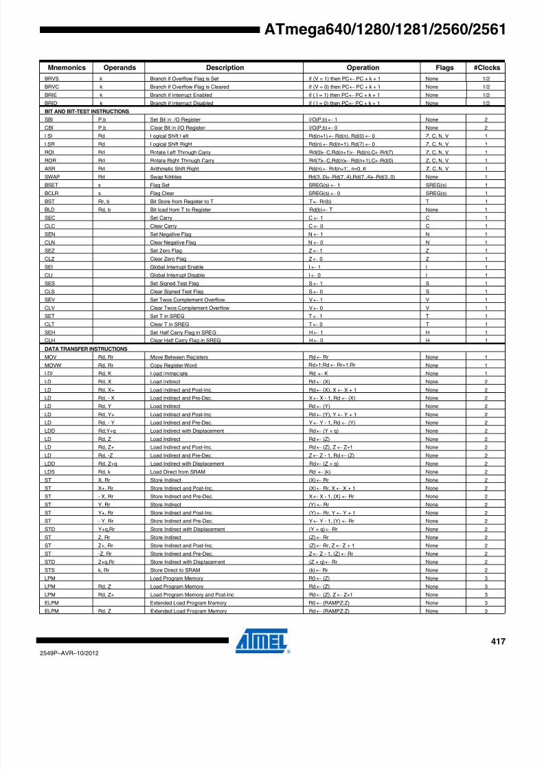
8/20/2019 At Mega 1281 Unlocked
http://slidepdf.com/reader/full/at-mega-1281-unlocked 417/446
417
2549P–AVR–10/2012
ATmega640/1280/1281/2560/2561
BRVS k Branch if Overflow Flag is Set if (V = 1) then PC ← PC + k + 1 None 1/2
BRVC k Branch if Overflow Flag is Cleared if (V = 0) then PC ← PC + k + 1 None 1/2
BRIE k Branch if Interrupt Enabled if ( I = 1) then PC ← PC + k + 1 None 1/2
BRID k Branch if Interrupt Disabled if ( I = 0) then PC ← PC + k + 1 None 1/2
BIT AND BIT-TEST INSTRUCTIONS
SBI P,b Set Bit in I/O Register I/O(P,b) ← 1 None 2
CBI P,b Clear Bit in I/O Register I/O(P,b) ← 0 None 2
LSL Rd Logical Shift Left Rd(n+1) ← Rd(n), Rd(0) ← 0 Z, C, N, V 1
LSR Rd Logical Shift Right Rd(n) ← Rd(n+1), Rd(7) ← 0 Z, C, N, V 1
ROL Rd Rotate Left Through Carry Rd(0)←C,Rd(n+1)← Rd(n),C←Rd(7) Z, C, N, V 1
ROR Rd Rotate Right Through Carry Rd(7)←C,Rd(n)← Rd(n+1),C←Rd(0) Z, C, N, V 1
ASR Rd Arithmetic Shift Right Rd(n) ← Rd(n+1), n=0..6 Z, C, N, V 1
SWAP Rd Swap Nibbles Rd(3..0)←Rd(7..4),Rd(7..4)←Rd(3..0) None 1
BSET s Flag Set SREG(s) ← 1 SREG(s) 1
BCLR s Flag Clear SREG(s) ← 0 SREG(s) 1
BST Rr, b Bit Store from Register to T T ← Rr(b) T 1
BLD Rd, b Bit load from T to Register Rd(b) ← T None 1
SEC Set Carry C ← 1 C 1
CLC Clear Carry C ← 0 C 1
SEN Set Negative Flag N ← 1 N 1
CLN Clear Negative Flag N ← 0 N 1
SEZ Set Zero Flag Z ← 1 Z 1
CLZ Clear Zero Flag Z ← 0 Z 1
SEI Global Interrupt Enable I ← 1 I 1
CLI Global Interrupt Disable I ← 0 I 1
SES Set Signed Test Flag S ← 1 S 1
CLS Clear Signed Test Flag S ← 0 S 1
SEV Set Twos Complement Overflow. V ← 1 V 1
CLV Clear Twos Complement Overflow V ← 0 V 1
SET Set T in SREG T ← 1 T 1
CLT Clear T in SREG T ← 0 T 1
SEH Set Half Carry Flag in SREG H ← 1 H 1
CLH Clear Half Carry Flag in SREG H ← 0 H 1
DATA TRANSFER INSTRUCTIONS
MOV Rd, Rr Move Between Registers Rd ← Rr None 1
MOVW Rd, Rr Copy Register Word Rd+1:Rd ← Rr+1:Rr None 1
LDI Rd, K Load Immediate Rd ← K None 1
LD Rd, X Load Indirect Rd ← (X) None 2
LD Rd, X+ Load Indirect and Post-Inc. Rd ← (X), X ← X + 1 None 2
LD Rd, - X Load Indirect and Pre-Dec. X ← X - 1, Rd ← (X) None 2
LD Rd, Y Load Indirect Rd ← (Y) None 2
LD Rd, Y+ Load Indirect and Post-Inc. Rd ← (Y), Y ← Y + 1 None 2
LD Rd, - Y Load Indirect and Pre-Dec. Y ← Y - 1, Rd ← (Y) None 2
LDD Rd,Y+q Load Indirect with Displacement Rd ← (Y + q) None 2
LD Rd, Z Load Indirect Rd ← (Z) None 2
LD Rd, Z+ Load Indirect and Post-Inc. Rd ← (Z), Z ← Z+1 None 2
LD Rd, -Z Load Indirect and Pre-Dec. Z ← Z - 1, Rd ← (Z) None 2
LDD Rd, Z+q Load Indirect with Displacement Rd ← (Z + q) None 2
LDS Rd, k Load Direct from SRAM Rd ← (k) None 2
ST X, Rr Store Indirect (X) ← Rr None 2
ST X+, Rr Store Indirect and Post-Inc. (X) ← Rr, X ← X + 1 None 2
ST - X, Rr Store Indirect and Pre-Dec. X ← X - 1, (X) ← Rr None 2
ST Y, Rr Store Indirect (Y) ← Rr None 2
ST Y+, Rr Store Indirect and Post-Inc. (Y) ← Rr, Y ← Y + 1 None 2
ST - Y, Rr Store Indirect and Pre-Dec. Y ← Y - 1, (Y) ← Rr None 2
STD Y+q,Rr Store Indirect with Displacement (Y + q) ← Rr None 2
ST Z, Rr Store Indirect (Z) ← Rr None 2
ST Z+, Rr Store Indirect and Post-Inc. (Z) ← Rr, Z ← Z + 1 None 2
ST -Z, Rr Store Indirect and Pre-Dec. Z ← Z - 1, (Z) ← Rr None 2
STD Z+q,Rr Store Indirect with Displacement (Z + q) ← Rr None 2
STS k, Rr Store Direct to SRAM (k) ← Rr None 2
LPM Load Program Memory R0 ← (Z) None 3
LPM Rd, Z Load Program Memory Rd ← (Z) None 3
LPM Rd, Z+ Load Program Memory and Post-Inc Rd ← (Z), Z ← Z+1 None 3
ELPM Extended Load Program Memory R0 ← (RAMPZ:Z) None 3
ELPM Rd, Z Extended Load Program Memory Rd ← (RAMPZ:Z) None 3
Mnemonics Operands Description Operation Flags #Clocks

8/20/2019 At Mega 1281 Unlocked
http://slidepdf.com/reader/full/at-mega-1281-unlocked 418/446
418
2549P–AVR–10/2012
ATmega640/1280/1281/2560/2561
Note: EICALL and EIJMP do not exist in ATmega640/1280/1281.ELPM does not exist in ATmega640.
ELPM Rd, Z+ Extended Load Program Memory Rd ← (RAMPZ:Z), RAMPZ:Z ←RAMPZ:Z+1 None 3
SPM Store Program Memory (Z) ← R1:R0 None -
IN Rd, P In Port Rd ← P None 1
OUT P, Rr Out Port P ← Rr None 1
PUSH Rr Push Register on Stack STACK ← Rr None 2
POP Rd Pop Register from Stack Rd ← STACK None 2
MCU CONTROL INSTRUCTIONS
NOP No Operation None 1
SLEEP Sleep (see specific descr. for Sleep function) None 1
WDR Watchdog Reset (see specific descr. for WDR/timer) None 1
BREAK Break For On-chip Debug Only None N /A
Mnemonics Operands Description Operation Flags #Clocks
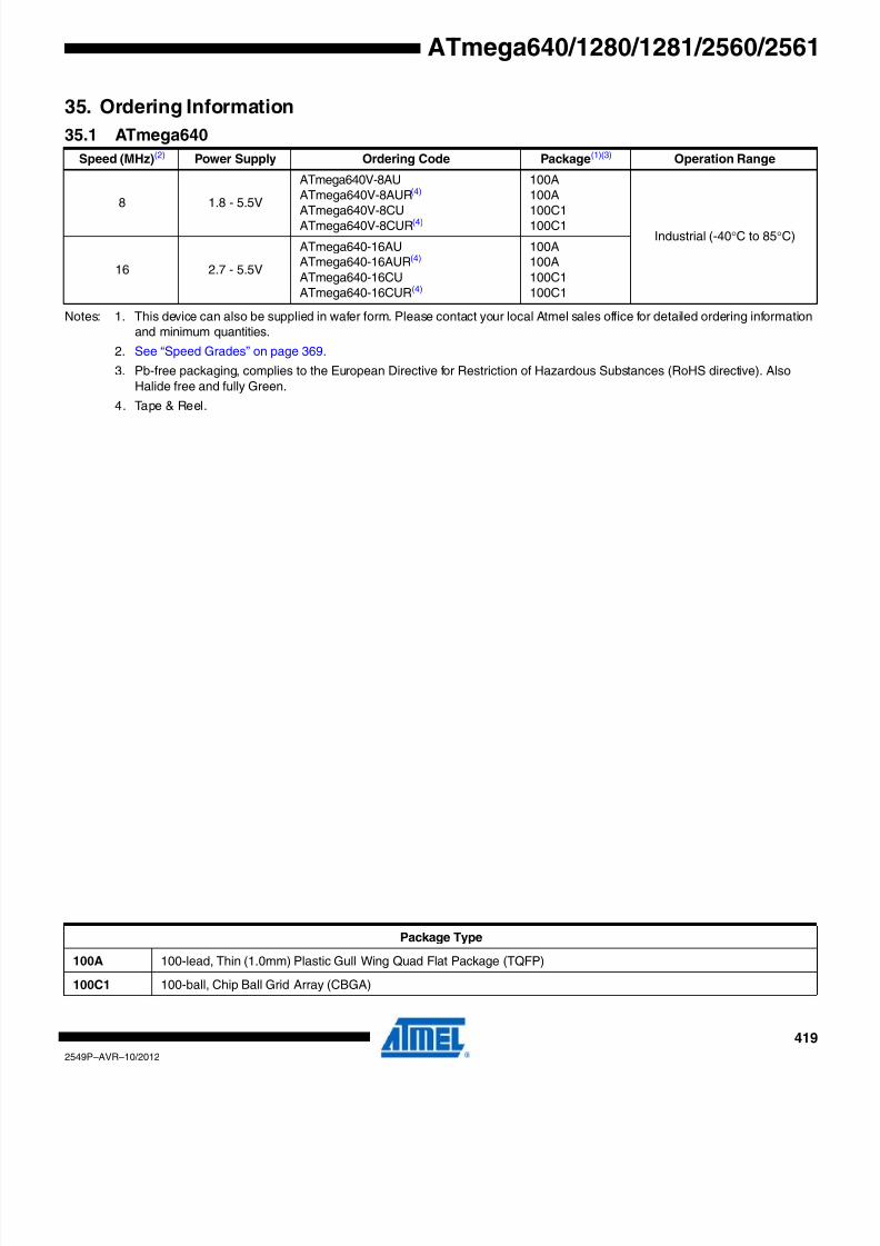
8/20/2019 At Mega 1281 Unlocked
http://slidepdf.com/reader/full/at-mega-1281-unlocked 419/446
419
2549P–AVR–10/2012
ATmega640/1280/1281/2560/2561
35. Ordering Information
Notes: 1. This device can also be supplied in wafer form. Please contact your local Atmel sales office for detailed ordering informationand minimum quantities.
2. See “Speed Grades” on page 369.
3. Pb-free packaging, complies to the European Directive for Restriction of Hazardous Substances (RoHS directive). AlsoHalide free and fully Green.
4. Tape & Reel.
35.1 ATmega640
Speed (MHz)(2) Power Supply Ordering Code Package(1)(3) Operation Range
8 1.8 - 5.5V
ATmega640V-8AUATmega640V-8AUR(4)
ATmega640V-8CUATmega640V-8CUR(4)
100A100A
100C1100C1
Industrial (-40°C to 85°C)
16 2.7 - 5.5V
ATmega640-16AUATmega640-16AUR(4)
ATmega640-16CUATmega640-16CUR(4)
100A100A100C1100C1
Package Type
100A 100-lead, Thin (1.0mm) Plastic Gull Wing Quad Flat Package (TQFP)
100C1 100-ball, Chip Ball Grid Array (CBGA)

8/20/2019 At Mega 1281 Unlocked
http://slidepdf.com/reader/full/at-mega-1281-unlocked 420/446
420
2549P–AVR–10/2012
ATmega640/1280/1281/2560/2561
Notes: 1. This device can also be supplied in wafer form. Please contact your local Atmel sales office for detailed ordering informationand minimum quantities.
2. See “Speed Grades” on page 369.
3. Pb-free packaging, complies to the European Directive for Restriction of Hazardous Substances (RoHS directive). AlsoHalide free and fully Green.
4. Tape & Reel.
35.2 ATmega1280
Speed (MHz)(2) Power Supply Ordering Code Package(1)(3) Operation Range
8 1.8V - 5.5V
ATmega1280V-8AUATmega1280V-8AUR(4)
ATmega1280V-8CUATmega1280V-8CUR(4)
100A100A100C1100C1
Industrial (-40°C to 85°C)
16 2.7V - 5.5V
ATmega1280-16AUATmega1280-16AUR(4)
ATmega1280-16CUATmega1280-16CUR(4)
100A100A100C1100C1
Package Type
100A 100-lead, Thin (1.0mm) Plastic Gull Wing Quad Flat Package (TQFP)
100C1 100-ball, Chip Ball Grid Array (CBGA)
8/20/2019 At Mega 1281 Unlocked
http://slidepdf.com/reader/full/at-mega-1281-unlocked 421/446
421
2549P–AVR–10/2012
ATmega640/1280/1281/2560/2561
Notes: 1. This device can also be supplied in wafer form. Please contact your local Atmel sales office for detailed ordering informationand minimum quantities.
2. See “Speed Grades” on page 369.
3. Pb-free packaging, complies to the European Directive for Restriction of Hazardous Substances (RoHS directive). AlsoHalide free and fully Green.
4. Tape & Reel.
35.3 ATmega1281
Speed (MHz)(2) Power Supply Ordering Code Package(1)(3) Operation Range
8 1.8 - 5.5V
ATmega1281V-8AUATmega1281V-8AUR(4)
ATmega1281V-8MU
ATmega1281V-8MUR
(4)
64A64A64M2
64M2 Industrial(-40°C to 85°C)
16 2.7 - 5.5V
ATmega1281-16AUATmega1281-16AUR(4)
ATmega1281-16MUATmega1281-16MUR(4)
64A64A64M264M2
Package Type
64A 64-lead, Thin (1.0mm) Plastic Gull Wing Quad Flat Package (TQFP)
64M2 64-pad, 9mm × 9mm × 1.0mm Body, Quad Flat No-lead/Micro Lead Frame Package (QFN /MLF)
8/20/2019 At Mega 1281 Unlocked
http://slidepdf.com/reader/full/at-mega-1281-unlocked 422/446
422
2549P–AVR–10/2012
ATmega640/1280/1281/2560/2561
Notes: 1. This device can also be supplied in wafer form. Please contact your local Atmel sales office for detailed ordering informationand minimum quantities.
2. See “Speed Grades” on page 369.
3. Pb-free packaging, complies to the European Directive for Restriction of Hazardous Substances (RoHS directive). AlsoHalide free and fully Green.
4. Tape & Reel.
35.4 ATmega2560
Speed (MHz)(2) Power Supply Ordering Code Package(1)(3) Operation Range
8 1.8V - 5.5V
ATmega2560V-8AUATmega2560V-8AUR(4)
ATmega2560V-8CUATmega2560V-8CUR(4)
100A100A100C1100C1
Industrial (-40°C to 85°C)
16 4.5V - 5.5V
ATmega2560-16AUATmega2560-16AUR(4)
ATmega2560-16CUATmega2560-16CUR(4)
100A100A100C1100C1
Package Type
100A 100-lead, Thin (1.0mm) Plastic Gull Wing Quad Flat Package (TQFP)
100C1 100-ball, Chip Ball Grid Array (CBGA)
8/20/2019 At Mega 1281 Unlocked
http://slidepdf.com/reader/full/at-mega-1281-unlocked 423/446
423
2549P–AVR–10/2012
ATmega640/1280/1281/2560/2561
Notes: 1. This device can also be supplied in wafer form. Please contact your local Atmel sales office for detailed ordering informationand minimum quantities.
2. See “Speed Grades” on page 369.
3. Pb-free packaging, complies to the European Directive for Restriction of Hazardous Substances (RoHS directive). AlsoHalide free and fully Green.
4. Tape & Reel.
35.5 ATmega2561
Speed (MHz)(2) Power Supply Ordering Code Package(1)(3) Operation Range
8 1.8V - 5.5V
ATmega1281V-8AUATmega1281V-8AUR(4)
ATmega1281V-8MUATmega1281V-8MUR(4)
64A64A64M264M2 Industrial
(-40°C to 85°C)
16 4.5V - 5.5V
ATmega1281-16AUATmega1281-16AUR(4)
ATmega1281-16MUATmega1281-16MUR(4)
64A64A64M264M2
Package Type
64A 64-lead, Thin (1.0mm) Plastic Gull Wing Quad Flat Package (TQFP)
64M2 64-pad, 9mm × 9mm × 1.0mm Body, Quad Flat No-lead/Micro Lead Frame Package (QFN /MLF)

8/20/2019 At Mega 1281 Unlocked
http://slidepdf.com/reader/full/at-mega-1281-unlocked 424/446
424
2549P–AVR–10/2012
ATmega640/1280/1281/2560/2561
36. Packaging Information
36.1 100A
2325 Orchard Parkway
San Jose, CA 95131
TITLE DRAWING NO.
R
REV.
100A, 100-lead, 14 x 14mm Body Size, 1.0mm Body Thickness,
0.5mm Lead Pitch, Thin Profile Plastic Quad Flat Package (TQFP)D100A
2010-10-20
PIN 1 IDENTIFIER
0°~7°
PIN 1
L
C
A1 A2 A
D1
D
e E1 E
B
A – – 1.20
A1 0.05 – 0.15
A2 0.95 1.00 1.05
D 15.75 16.00 16.25
D1 13.90 14.00 14.10 Note 2
E 15.75 16.00 16.25
E1 13.90 14.00 14.10 Note 2
B 0.17 – 0.27
C 0.09 – 0.20
L 0.45 – 0.75
e 0.50 TYP
Notes:
1. This package conforms to JEDEC reference MS-026, Variation AED.
2. Dimensions D1 and E1 do not include mold protrusion. Allowable
protrusion is 0.25mm per side. Dimensions D1 and E1 are maximum
plastic body size dimensions including mold mismatch. 3. Lead coplanarity is 0.08mm maximum.
COMMON DIMENSIONS
(Unit of Measure = mm)
SYMBOL MIN NOM MAX NOTE

8/20/2019 At Mega 1281 Unlocked
http://slidepdf.com/reader/full/at-mega-1281-unlocked 425/446
425
2549P–AVR–10/2012
ATmega640/1280/1281/2560/2561
36.2 100C1
2325 Orchard Parkway
San Jose, CA 95131
TITLE DRAWING NO.
R
REV.
100C1, 100-ball, 9 x 9 x 1.2 mm Body, Ball Pitch 0.80 mm
Chip Array BGA Package (CBGA) A100C1
5/25/06
TOP VIEW
SIDE VIEW
BOTTOM VIEW
COMMON DIMENSIONS
(Unit of Measure = mm)
SYMBOL MIN NOM MAX NOTE
A 1.10 – 1.20
A1 0.30 0.35 0.40
D 8.90 9.00 9.10
E 8.90 9.00 9.10
D1 7.10 7.20 7.30
E1 7.10 7.20 7.30
Øb 0.35 0.40 0.45
e 0.80 TYP
Marked A1 Identifier
12345678
A
B
C
D
E
9
F
G
H
I
J
10
0.90 TYP
0.90 TYP
A1 Corner
0.12 Z
E
D
e
e
Øb
A
A1
E1
D1

8/20/2019 At Mega 1281 Unlocked
http://slidepdf.com/reader/full/at-mega-1281-unlocked 426/446
426
2549P–AVR–10/2012
ATmega640/1280/1281/2560/2561
36.3 64A
2325 Orchard Parkway
San Jose, CA 95131
TITLE DRAWING NO.
R
REV.
64A, 64-lead, 14 x 14mm Body Size, 1.0mm Body Thickness,0.8mm Lead Pitch, Thin Profile Plastic Quad Flat Package (TQFP)
C64A
2010-10-20
PIN 1 IDENTIFIER
0°~7°
PIN 1
L
C
A1 A2 A
D1
D
e
E1 E
B
COMMON DIMENSIONS
(Unit of measure = mm)
SYMBOL MIN NOM MAX NOTE
Notes:
1.This package conforms to JEDEC reference MS-026, Variation AEB.
2. Dimensions D1 and E1 do not include mold protrusion. Allowable
protrusion is 0.25mm per side. Dimensions D1 and E1 are maximum
plastic body size dimensions including mold mismatch.
3. Lead coplanarity is 0.10mm maximum.
A – – 1.20
A1 0.05 – 0.15
A2 0.95 1.00 1.05
D 15.75 16.00 16.25
D1 13.90 14.00 14.10 Note 2
E 15.75 16.00 16.25
E1 13.90 14.00 14.10 Note 2
B 0.30 – 0.45
C 0.09 – 0.20
L 0.45 – 0.75
e 0.80 TYP
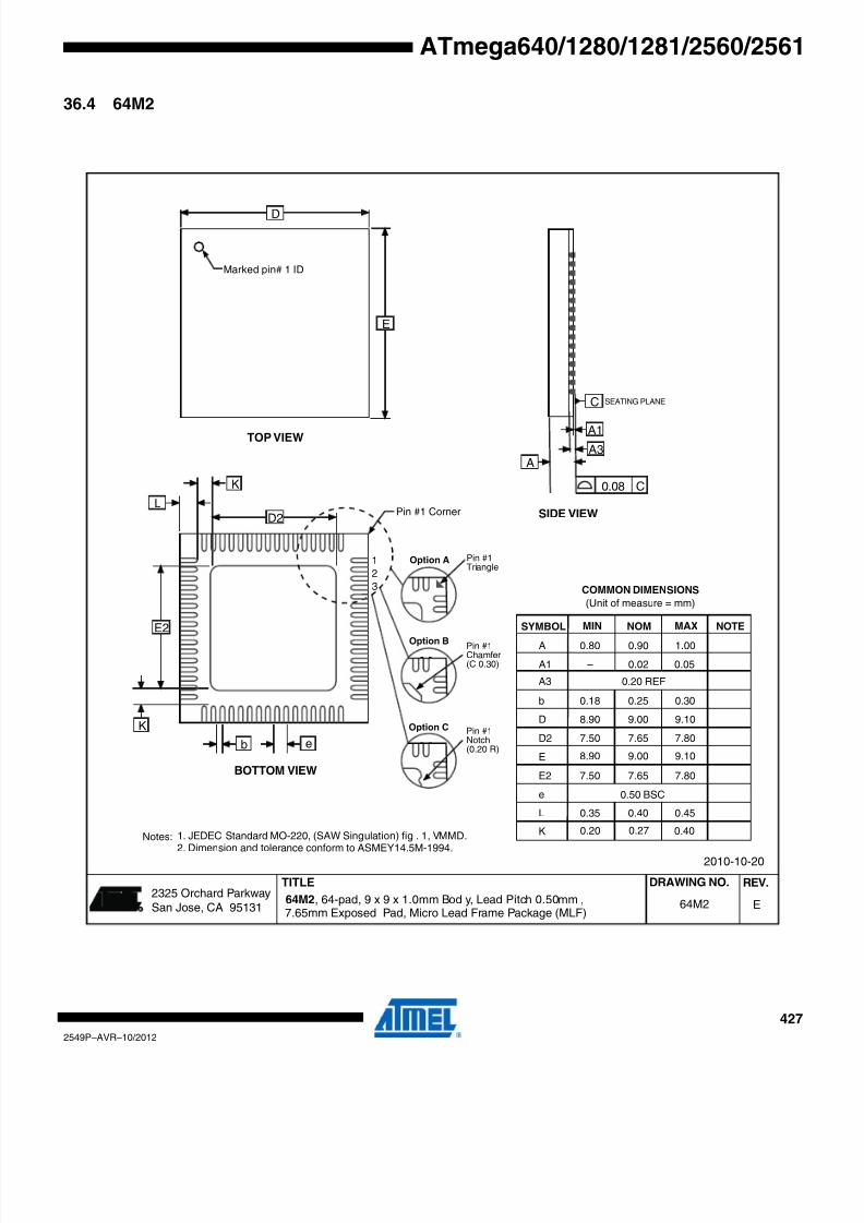
8/20/2019 At Mega 1281 Unlocked
http://slidepdf.com/reader/full/at-mega-1281-unlocked 427/446
427
2549P–AVR–10/2012
ATmega640/1280/1281/2560/2561
36.4 64M2
2325 Orchard Parkway
San Jose, CA 95131
TITLE DRAWING NO.
R
REV.
64M2, 64-pad, 9 x 9 x 1.0mm Bod y, Lead Pitch 0.50mm , E64M2
2010-10-20
COMMON DIMENSIONS
(Unit of measure = mm)
SYMBOL MIN NOM MAX NOTE
A 0.80 0.90 1.00
A1 – 0.02 0.05
b
0.18 0.25 0.30
D
D2
7.50 7.65 7.80
8.90 9.00 9.10
8.90 9.00 9.10
E
E2
7.50 7.65 7.80
e
0.50 BSC
L 0.35 0.40
0.45
TOP VIEW
SIDE VIEW
BOTTOM VIEW
D
E
Marked pin# 1 ID
SEATING PLANE
A1
C
A
C0.08
1
2
3
K0.20 0.27 0.40
2. Dimension and tolerance conform to ASMEY14.5M-1994.
0.20 REFA3
A3
E2
D2
b e
Pin #1 CornerL
Pin #1Triangle
Pin #1Chamfer(C 0.30)
Option A
Option B
Pin #1Notch(0.20 R)
Option C
K
K
Notes: 1. JEDEC Standard MO-220, (SAW Singulation) fig . 1, VMMD.
7.65mm Exposed Pad, Micro Lead Frame Package (MLF)

8/20/2019 At Mega 1281 Unlocked
http://slidepdf.com/reader/full/at-mega-1281-unlocked 428/446
428
2549P–AVR–10/2012
ATmega640/1280/1281/2560/2561
37. Errata
37.1 ATmega640 rev. B• Inaccurate ADC conversion in differential mode with 200× gain
• High current consumption in sleep mode
1. Inaccurate ADC conversion in differential mode with 200× gain
With AVCC <3.6V, random conversions will be inaccurate. Typical absolute accuracy may
reach 64 LSB.
Problem Fix/Workaround
None.
2. High current consumption in sleep mode
If a pending interrupt cannot wake the part up from the selected sleep mode, the curren
consumption will increase during sleep when executing the SLEEP instruction directly afte
a SEI instruction.
Problem Fix/WorkaroundBefore entering sleep, interrupts not used to wake the part from the sleep mode should be
disabled.
37.2 ATmega640 rev. A• Inaccurate ADC conversion in differential mode with 200× gain
• High current consumption in sleep mode
1. Inaccurate ADC conversion in differential mode with 200× gain
With AVCC <3.6V, random conversions will be inaccurate. Typical absolute accuracy may
reach 64 LSB.
Problem Fix/WorkaroundNone.
2. High current consumption in sleep mode
If a pending interrupt cannot wake the part up from the selected sleep mode, the curren
consumption will increase during sleep when executing the SLEEP instruction directly afte
a SEI instruction.
Problem Fix/Workaround
Before entering sleep, interrupts not used to wake the part from the sleep mode should be
disabled.
37.3 ATmega1280 rev. B• Inaccurate ADC conversion in differential mode with 200× gain
• High current consumption in sleep mode
1. Inaccurate ADC conversion in differential mode with 200× gain
With AVCC <3.6V, random conversions will be inaccurate. Typical absolute accuracy may
reach 64 LSB.

8/20/2019 At Mega 1281 Unlocked
http://slidepdf.com/reader/full/at-mega-1281-unlocked 429/446
429
2549P–AVR–10/2012
ATmega640/1280/1281/2560/2561
Problem Fix/Workaround
None.
2. High current consumption in sleep mode
If a pending interrupt cannot wake the part up from the selected sleep mode, the curren
consumption will increase during sleep when executing the SLEEP instruction directly afte
a SEI instruction.
Problem Fix/Workaround
Before entering sleep, interrupts not used to wake the part from the sleep mode should be
disabled.
37.4 ATmega1280 rev. A• Inaccurate ADC conversion in differential mode with 200× gain
• High current consumption in sleep mode
1. Inaccurate ADC conversion in differential mode with 200× gain
With AVCC <3.6V, random conversions will be inaccurate. Typical absolute accuracy may
reach 64 LSB.Problem Fix/Workaround
None.
2. High current consumption in sleep mode
If a pending interrupt cannot wake the part up from the selected sleep mode, the curren
consumption will increase during sleep when executing the SLEEP instruction directly afte
a SEI instruction.
Problem Fix/Workaround
Before entering sleep, interrupts not used to wake the part from the sleep mode should be
disabled.
37.5 ATmega1281 rev. B• Inaccurate ADC conversion in differential mode with 200× gain
• High current consumption in sleep mode
1. Inaccurate ADC conversion in differential mode with 200× gain
With AVCC <3.6V, random conversions will be inaccurate. Typical absolute accuracy may
reach 64 LSB.
Problem Fix/Workaround
None.
2. High current consumption in sleep modeIf a pending interrupt cannot wake the part up from the selected sleep mode, the curren
consumption will increase during sleep when executing the SLEEP instruction directly afte
a SEI instruction.
Problem Fix/Workaround
Before entering sleep, interrupts not used to wake the part from the sleep mode should be
disabled.

8/20/2019 At Mega 1281 Unlocked
http://slidepdf.com/reader/full/at-mega-1281-unlocked 430/446
430
2549P–AVR–10/2012
ATmega640/1280/1281/2560/2561
37.6 ATmega1281 rev. A• Inaccurate ADC conversion in differential mode with 200× gain
• High current consumption in sleep mode
1. Inaccurate ADC conversion in differential mode with 200× gain
With AVCC <3.6V, random conversions will be inaccurate. Typical absolute accuracy may
reach 64 LSB.Problem Fix/Workaround
None.
2. High current consumption in sleep mode
If a pending interrupt cannot wake the part up from the selected sleep mode, the curren
consumption will increase during sleep when executing the SLEEP instruction directly afte
a SEI instruction.
Problem Fix/Workaround
Before entering sleep, interrupts not used to wake the part from the sleep mode should be
disabled.
37.7 ATmega2560 rev. F
Not sampled.
37.8 ATmega2560 rev. E
No known errata.
37.9 ATmega2560 rev. D
Not sampled.
37.10 ATmega2560 rev. C• High current consumption in sleep mode
1. High current consumption in sleep mode
If a pending interrupt cannot wake the part up from the selected sleep mode, the curren
consumption will increase during sleep when executing the SLEEP instruction directly afte
a SEI instruction.
Problem Fix/Workaround
Before entering sleep, interrupts not used to wake the part from the sleep mode should be
disabled.
37.11 ATmega2560 rev. B
Not sampled.

8/20/2019 At Mega 1281 Unlocked
http://slidepdf.com/reader/full/at-mega-1281-unlocked 431/446
431
2549P–AVR–10/2012
ATmega640/1280/1281/2560/2561
37.12 ATmega2560 rev. A• Non-Read-While-Write area of flash not functional
• Part does not work under 2.4 volts
• Incorrect ADC reading in differential mode
• Internal ADC reference has too low value
• IN/OUT instructions may be executed twice when Stack is in external RAM
• EEPROM read from application code does not work in Lock Bit Mode 3
1. Non-Read-While-Write area of flash not functional
The Non-Read-While-Write area of the flash is not working as expected. The problem is
related to the speed of the part when reading the flash of this area.
Problem Fix/Workaround
- Only use the first 248K of the flash.
- If boot functionality is needed, run the code in the Non-Read-While-Write area at maximum
1/4th of the maximum frequency of the device at any given voltage. This is done by writing
the CLKPR register before entering the boot section of the code.
2. Part does not work under 2.4 volts
The part does not execute code correctly below 2.4 volts.
Problem Fix/Workaround
Do not use the part at voltages below 2.4 volts.
3. Incorrect ADC reading in differential mode
The ADC has high noise in differential mode. It can give up to 7 LSB error.
Problem Fix/Workaround
Use only the 7 MSB of the result when using the ADC in differential mode.
4. Internal ADC reference has too low value
The internal ADC reference has a value lower than specified.Problem Fix/Workaround
- Use AVCC or external reference.
- The actual value of the reference can be measured by applying a known voltage to the
ADC when using the internal reference. The result when doing later conversions can then be
calibrated.
5. IN/OUT instructions may be executed twice when Stack is in external RAM
If either an IN or an OUT instruction is executed directly before an interrupt occurs and the
stack pointer is located in external ram, the instruction will be executed twice. In some cases
this will cause a problem, for example:
- If reading SREG it will appear that the I-flag is cleared.
- If writing to the PIN registers, the port will toggle twice.
- If reading registers with interrupt flags, the flags will appear to be cleared.

8/20/2019 At Mega 1281 Unlocked
http://slidepdf.com/reader/full/at-mega-1281-unlocked 432/446
432
2549P–AVR–10/2012
ATmega640/1280/1281/2560/2561
Problem Fix/Workaround
There are two application work-arounds, where selecting one of them, will be omitting the
issue:
- Replace IN and OUT with LD/LDS/LDD and ST/STS/STD instructions.
- Use internal RAM for stack pointer.
6. EEPROM read from application code does not work in Lock Bit Mode 3
When the Memory Lock Bits LB2 and LB1 are programmed to mode 3, EEPROM read does
not work from the application code.
Problem Fix/Workaround
Do not set Lock Bit Protection Mode 3 when the application code needs to read from
EEPROM.
37.13 ATmega2561 rev. F
Not sampled.
37.14 ATmega2561 rev. ENo known errata.
37.15 ATmega2561 rev. D
Not sampled.
37.16 ATmega2561 rev. C• High current consumption in sleep mode.
1. High current consumption in sleep mode
If a pending interrupt cannot wake the part up from the selected sleep mode, the curren
consumption will increase during sleep when executing the SLEEP instruction directly aftea SEI instruction.
Problem Fix/Workaround
Before entering sleep, interrupts not used to wake the part from the sleep mode should be
disabled.
37.17 ATmega2561 rev. B
Not sampled.
37.18 ATmega2561 rev. A• Non-Read-While-Write area of flash not functional
• Part does not work under 2.4 Volts
• Incorrect ADC reading in differential mode
• Internal ADC reference has too low value
• IN/OUT instructions may be executed twice when Stack is in external RAM
• EEPROM read from application code does not work in Lock Bit Mode 3

8/20/2019 At Mega 1281 Unlocked
http://slidepdf.com/reader/full/at-mega-1281-unlocked 433/446
433
2549P–AVR–10/2012
ATmega640/1280/1281/2560/2561
1. Non-Read-While-Write area of flash not functional
The Non-Read-While-Write area of the flash is not working as expected. The problem is
related to the speed of the part when reading the flash of this area.
Problem Fix/Workaround
- Only use the first 248K of the flash.
- If boot functionality is needed, run the code in the Non-Read-While-Write area at maximum1/4th of the maximum frequency of the device at any given voltage. This is done by writing
the CLKPR register before entering the boot section of the code.
2. Part does not work under 2.4 volts
The part does not execute code correctly below 2.4 volts.
Problem Fix/Workaround
Do not use the part at voltages below 2.4 volts.
3. Incorrect ADC reading in differential mode
The ADC has high noise in differential mode. It can give up to 7 LSB error.
Problem Fix/Workaround
Use only the 7 MSB of the result when using the ADC in differential mode.
4. Internal ADC reference has too low value
The internal ADC reference has a value lower than specified.
Problem Fix/Workaround
- Use AVCC or external reference.
- The actual value of the reference can be measured by applying a known voltage to the
ADC when using the internal reference. The result when doing later conversions can then be
calibrated.
5. IN/OUT instructions may be executed twice when Stack is in external RAM
If either an IN or an OUT instruction is executed directly before an interrupt occurs and the
stack pointer is located in external ram, the instruction will be executed twice. In some cases
this will cause a problem, for example:
- If reading SREG it will appear that the I-flag is cleared.
- If writing to the PIN registers, the port will toggle twice.
- If reading registers with interrupt flags, the flags will appear to be cleared.
Problem Fix/Workaround
There are two application workarounds, where selecting one of them, will be omitting the
issue:
- Replace IN and OUT with LD/LDS/LDD and ST/STS/STD instructions.
- Use internal RAM for stack pointer.
6. EEPROM read from application code does not work in Lock Bit Mode 3
When the Memory Lock Bits LB2 and LB1 are programmed to mode 3, EEPROM read does
not work from the application code.

8/20/2019 At Mega 1281 Unlocked
http://slidepdf.com/reader/full/at-mega-1281-unlocked 434/446
434
2549P–AVR–10/2012
ATmega640/1280/1281/2560/2561
Problem Fix/Workaround
Do not set Lock Bit Protection Mode 3 when the application code needs to read from
EEPROM.

8/20/2019 At Mega 1281 Unlocked
http://slidepdf.com/reader/full/at-mega-1281-unlocked 435/446
435
2549P–AVR–10/2012
ATmega640/1280/1281/2560/2561
38. Datasheet Revision History
Please note that the referring page numbers in this section are referring to this document.Thereferring revision in this section are referring to the document revision.
38.1 Rev. 2549P-10/2012
38.2 Rev. 2549O-05/12
38.3 Rev. 2549N-05/11
38.4 Rev. 2549M-09/10
1. Replaced drawing in 36.4 “64M2” on page 427.
2. Former page 439 has been deleted as the content of this page did not belong there (same pageas the last page).
3. Some small correction made in the setup.
1. The datasheet changed status from Preliminary to Complete. Removed “Preliminary” from thefront page.
2. Replaced Figure 10-3 on page 46 by a new one.
3. Updated the last page to include the new address for Atmel Japan site.
1. Added Atmel QTouch Library Support and QTouch Sensing Capablity Features
2. Updated Cross-reference in “Bit 5, 2:0 - WDP3:0: Watchdog Timer Prescaler 3, 2, 1 and 0” onpage 68
3. Updated Assembly codes in section “USART Initialization” on page 210
4. Added “Standard Power-On Reset” on page 372.
5. Added “Enhanced Power-On Reset” on page 373.
6. Updated Figure 32-13 on page 393
7. Updated “Ordering Information” on page 419 to include Tape & Reel devices.
1. Updated typos in Figure 26-9 on page 285 and in Figure 26-10 on page 285.
2. Note is added below Table 1-1 on page 3.
3. The values for “typical characteristics” in Table 31-9 on page 377 and Table 31-10 on page 378,has been rounded.
4. Units for tRST and tBOD in Table 31-3 on page 372 have been changed from “ns” to “µs”.
5. The figure text for Table 31-2 on page 371 has been changed.
6. Text in first column in Table 30-3 on page 336 has been changed from “Fuse Low Byte” to“Extended Fuse Byte”.
7. The text in “Power Reduction Register” on page 54 has been changed.
8. The value of the inductor in Figure 26-9 on page 285 and Figure 26-10 on page 285 has beenchanged to 10µH.
9. “Port A” has been changed into “Port K” in the first paragraph of “Features” on page 275.
8/20/2019 At Mega 1281 Unlocked
http://slidepdf.com/reader/full/at-mega-1281-unlocked 436/446
436
2549P–AVR–10/2012
ATmega640/1280/1281/2560/2561
38.5 Rev. 2549L-08/07
38.6 Rev. 2549K-01/07
38.7 Rev. 2549J-09/06
10. Minimum wait delay for tWD_EEPROM in Table 30-16 on page 351 has been changed from9.0ms to 3.6ms
11. Dimension A3 is added in “64M2” on page 427.
12. Several cross-references are corrected.
13. “COM0A1:0” on page 130 is corrected to “COM0B1:0”.
14. Corrected some Figure and Table numbering.
15. Updated Section 10.6 “Low Frequency Crystal Oscillator” on page 45.
1. Updated note in Table 10-11 on page 47.
2. Updated Table 10-3 on page 43, Table 10-5 on page 44, Table 10-9 on page 47.
3. Updated typos in “DC Characteristics” on page 367
4. Updated “Clock Characteristics” on page 371
5. Updated “External Clock Drive” on page 371.
6. Added “System and Reset Characteristics” on page 372.
7. Updated “SPI Timing Characteristics” on page 375.
8. Updated “ADC Characteristics – Preliminary Data” on page 377.
9. Updated ordering code in “ATmega640” on page 419.
1. Updated Table 1-1 on page 3.
2. Updated “Pin Descriptions” on page 7.
3. Updated “Stack Pointer” on page 16.
4. Updated “Bit 1 – EEPE: EEPROM Programming Enable” on page 36.
5. Updated Assembly code example in “Thus, when the BOD is not enabled, after setting the ACBGbit or enabling the ADC, the user must always allow the reference to start up before the output
from the Analog Comparator or ADC is used. To reduce power consumption in Power-downmode, the user can avoid the three conditions above to ensure that the reference is turned offbefore entering Power-down mode.” on page 63.
6: Updated “EIMSK – External Interrupt Mask Register” on page 115.
7. Updated Bit description in “PCIFR – Pin Change Interrupt Flag Register” on page 116.
8. Updated code example in “USART Initialization” on page 210.
9. Updated Figure 26-8 on page 284.
10. Updated “DC Characteristics” on page 367.
1. Updated “” on page 46.
2. Updated code example in “Moving Interrupts Between Application and Boot Section” on page109.
3. Updated “Timer/Counter Prescaler” on page 186.
4. Updated “Device Identification Register” on page 303.
5. Updated “Signature Bytes” on page 338.
6. Updated “Instruction Set Summary” on page 416.

8/20/2019 At Mega 1281 Unlocked
http://slidepdf.com/reader/full/at-mega-1281-unlocked 437/446
437
2549P–AVR–10/2012
ATmega640/1280/1281/2560/2561
38.8 Rev. 2549I-07/06
38.9 Rev. 2549H-06/06
38.10 Rev. 2549G-06/06
38.11 Rev. 2549F-04/06
38.12 Rev. 2549E-04/06
1. Added “Data Retention” on page 11.
2. Updated Table 16-3 on page 129, Table 16-6 on page 130, Table 16-8 on page 131, Table 17-2on page 148, Table 17-4 on page 159, Table 17-5 on page 160, Table 20-3 on page 187, Table20-6 on page 188 and Table 20-8 on page 189.
3. Updated “Fast PWM Mode” on page 150.
1. Updated “” on page 46.
2. Updated “OSCCAL – Oscillator Calibration Register” on page 50.
3. Added Table 31-1 on page 371.
1. Updated “Features” on page 1.
2. Added Figure 1-2 on page 3, Table 1-1 on page 3.
3. Updated “” on page 46.
4. Updated “Power Management and Sleep Modes” on page 52.
5. Updated note for Table 12-1 on page 68.
6. Updated Figure 26-9 on page 285 and Figure 26-10 on page 285.
7. Updated “Setting the Boot Loader Lock Bits by SPM” on page 324.
8. Updated “Ordering Information” on page 419.
9. Added Package information “100C1” on page 425.
10. Updated “Errata” on page 428.
1. Updated Figure 9-3 on page 31, Figure 9-4 on page 31 and Figure 9-5 on page 32.
2. Updated Table 20-2 on page 187 and Table 20-3 on page 187.
3. Updated Features in “ADC – Analog to Digital Converter” on page 275.
4. Updated “Fuse Bits” on page 336.
1. Updated “Features” on page 1.
2. Updated Table 12-1 on page 62.
3. Updated note for Table 12-1 on page 62.
4. Updated “Bit 6 – ACBG: Analog Comparator Bandgap Select” on page 273.
5. Updated “Prescaling and Conversion Timing” on page 278.
5. Updated “Maximum speed vs. VCC” on page 373.
6. Updated “Ordering Information” on page 419.

8/20/2019 At Mega 1281 Unlocked
http://slidepdf.com/reader/full/at-mega-1281-unlocked 438/446
438
2549P–AVR–10/2012
ATmega640/1280/1281/2560/2561
38.13 Rev. 2549D-12/05
38.14 Rev. 2549C-09/05
38.15 Rev. 2549B-05/05
38.16 Rev. 2549A-03/05
1. Advanced Information Status changed to Preliminary.
2. Changed number of I/O Ports from 51 to 54.
3. Updatet typos in “TCCR0A – Timer/Counter Control Register A” on page 129.
4. Updated Features in “ADC – Analog to Digital Converter” on page 275.5. Updated Operation in“ADC – Analog to Digital Converter” on page 275
6. Updated Stabilizing Time in “Changing Channel or Reference Selection” on page 282.
7. Updated Figure 26-1 on page 276, Figure 26-9 on page 285, Figure 26-10 on page 285.
8. Updated Text in “ADCSRB – ADC Control and Status Register B” on page 290.
9. Updated Note for Table 4 on page 43, Table 13-15 on page 86, Table 26-3 on page 289 andTable 26-6 on page 295.
10. Updated Table 31-9 on page 377 and Table 31-10 on page 378.
11. Updated “Filling the Temporary Buffer (Page Loading)” on page 323.
12. Updated “Typical Characteristics” on page 385.
13. Updated “Packaging Information” on page 424.
14. Updated “Errata” on page 428.
1. Updated Speed Grade in section “Features” on page 1.
2. Added “Resources” on page 11.
3. Updated “SPI – Serial Peripheral Interface” on page 195. In Slave mode, low and high period SPIclock must be larger than 2 CPU cycles.
4. Updated “Bit Rate Generator Unit” on page 247.
5. Updated “Maximum speed vs. VCC” on page 373.
6. Updated “Ordering Information” on page 419.
7. Updated “Packaging Information” on page 424. Package 64M1 replaced by 64M2.
8. Updated “Errata” on page 428.
1. JTAG ID/Signature for ATmega640 updated: 0x9608.
2. Updated Table 13-7 on page 81.
3. Updated “Serial Programming Instruction set” on page 352.
4. Updated “Errata” on page 428.
1. Initial version.
8/20/2019 At Mega 1281 Unlocked
http://slidepdf.com/reader/full/at-mega-1281-unlocked 439/446
2549P–AVR–10/2012
ATmega640/1280/1281/2560/2561
Table of Contents
Features ..................................................................................................... 1
1 Pin Configurations ................................................................................... 2
2 Overview ................................................................................................... 52.1 Block Diagram ...................................................................................................5
2.2 Comparison Between ATmega1281/2561 and ATmega640/1280/2560 ...........7
2.3 Pin Descriptions .................................................................................................7
3 Resources ............................................................................................... 11
4 About Code Examples ........................................................................... 11
5 Data Retention ........................................................................................ 11
6 Capacitive touch sensing ...................................................................... 11
7 AVR CPU Core ........................................................................................ 12
7.1 Introduction ......................................................................................................12
7.2 Architectural Overview .....................................................................................12
7.3 ALU – Arithmetic Logic Unit .............................................................................13
7.4 Status Register ................................................................................................14
7.5 General Purpose Register File ........................................................................15
7.6 Stack Pointer ...................................................................................................16
7.7 Instruction Execution Timing ...........................................................................17
7.8 Reset and Interrupt Handling ...........................................................................18
8 AVR Memories ........................................................................................ 21
8.1 In-System Reprogrammable Flash Program Memory .....................................21
8.2 SRAM Data Memory ........................................................................................21
8.3 EEPROM Data Memory ..................................................................................23
8.4 I/O Memory ......................................................................................................27
9 External Memory Interface .................................................................... 28
9.1 Overview ..........................................................................................................289.2 Register Description ........................................................................................35
9.3 General Purpose registers ...............................................................................37
9.4 External Memory registers ...............................................................................37
10 System Clock and Clock Options ......................................................... 40
10.1 Overview ..........................................................................................................40

8/20/2019 At Mega 1281 Unlocked
http://slidepdf.com/reader/full/at-mega-1281-unlocked 440/446
i
2549P–AVR–10/2012
ATmega640/1280/1281/2560/2561
10.2 Clock Systems and their Distribution ...............................................................40
10.3 Clock Sources .................................................................................................41
10.4 Low Power Crystal Oscillator ...........................................................................42
10.5 Full Swing Crystal Oscillator ............................................................................44
10.6 Low Frequency Crystal Oscillator ....................................................................4510.7 Calibrated Internal RC Oscillator .....................................................................47
10.8 128 kHz Internal Oscillator ..............................................................................47
10.9 External Clock .................................................................................................48
10.10 Clock Output Buffer .........................................................................................49
10.11 Timer/Counter Oscillator ..................................................................................49
10.12 System Clock Prescaler ..................................................................................49
10.13 Register Description ........................................................................................50
11 Power Management and Sleep Modes ................................................. 52
11.1 Sleep Modes ....................................................................................................52
11.2 Idle Mode .........................................................................................................52
11.3 ADC Noise Reduction Mode ............................................................................53
11.4 Power-down Mode ...........................................................................................53
11.5 Power-save Mode ............................................................................................53
11.6 Standby Mode .................................................................................................54
11.7 Extended Standby Mode .................................................................................54
11.8 Power Reduction Register ...............................................................................54
11.9 Minimizing Power Consumption ......................................................................54
11.10 Register Description ........................................................................................56
12 System Control and Reset .................................................................... 59
12.1 Resetting the AVR ...........................................................................................59
12.2 Reset Sources .................................................................................................59
12.3 Internal Voltage Reference ..............................................................................62
12.4 Watchdog Timer ..............................................................................................63
12.5 Register Description ........................................................................................67
13 I/O-Ports .................................................................................................. 70
13.1 Introduction ......................................................................................................70
13.2 Ports as General Digital I/O .............................................................................71
13.3 Alternate Port Functions ..................................................................................75
13.4 Register Description for I/O-Ports ..................................................................100
14 Interrupts .............................................................................................. 105

8/20/2019 At Mega 1281 Unlocked
http://slidepdf.com/reader/full/at-mega-1281-unlocked 441/446
ii
2549P–AVR–10/2012
ATmega640/1280/1281/2560/2561
14.1 Interrupt Vectors in ATmega640/1280/1281/2560/2561 ................................105
14.2 Reset and Interrupt Vector placement ...........................................................107
14.3 Moving Interrupts Between Application and Boot Section .............................109
14.4 Register Description ......................................................................................110
15 External Interrupts ............................................................................... 11215.1 Pin Change Interrupt Timing ..........................................................................112
15.2 Register Description ......................................................................................113
16 8-bit Timer/Counter0 with PWM .......................................................... 118
16.1 Features ........................................................................................................118
16.2 Overview ........................................................................................................118
16.3 Timer/Counter Clock Sources .......................................................................119
16.4 Counter Unit ..................................................................................................119
16.5 Output Compare Unit .....................................................................................12016.6 Compare Match Output Unit ..........................................................................122
16.7 Modes of Operation .......................................................................................123
16.8 Timer/Counter Timing Diagrams ...................................................................127
16.9 Register Description ......................................................................................129
17 16-bit Timer/Counter (Timer/Counter 1, 3, 4, and 5) .......................... 136
17.1 Features ........................................................................................................136
17.2 Overview ........................................................................................................136
17.3 Accessing 16-bit Registers ............................................................................13817.4 Timer/Counter Clock Sources .......................................................................141
17.5 Counter Unit ..................................................................................................142
17.6 Input Capture Unit .........................................................................................143
17.7 Output Compare Units ...................................................................................145
17.8 Compare Match Output Unit ..........................................................................147
17.9 Modes of Operation .......................................................................................148
17.10 Timer/Counter Timing Diagrams ...................................................................156
17.11 Register Description ......................................................................................158
18 Timer/Counter 0, 1, 3, 4, and 5 Prescaler ........................................... 169
18.1 Internal Clock Source ....................................................................................169
18.2 Prescaler Reset .............................................................................................169
18.3 External Clock Source ...................................................................................169
18.4 Register Description ......................................................................................170

8/20/2019 At Mega 1281 Unlocked
http://slidepdf.com/reader/full/at-mega-1281-unlocked 442/446
iv
2549P–AVR–10/2012
ATmega640/1280/1281/2560/2561
19 Output Compare Modulator (OCM1C0A) ........................................... 172
19.1 Overview ........................................................................................................172
19.2 Description .....................................................................................................172
20 8-bit Timer/Counter2 with PWM and Asynchronous Operation ...... 174
20.1 Overview ........................................................................................................174
20.2 Timer/Counter Clock Sources .......................................................................175
20.3 Counter Unit ..................................................................................................175
20.4 Modes of Operation .......................................................................................176
20.5 Output Compare Unit .....................................................................................180
20.6 Compare Match Output Unit ..........................................................................182
20.7 Timer/Counter Timing Diagrams ...................................................................183
20.8 Asynchronous Operation of Timer/Counter2 .................................................184
20.9 Timer/Counter Prescaler ...............................................................................186
20.10 Register Description ......................................................................................187
21 SPI – Serial Peripheral Interface ......................................................... 195
21.1 SS Pin Functionality ......................................................................................200
21.2 Register Description ......................................................................................202
22 USART ................................................................................................... 205
22.1 Features ........................................................................................................205
22.2 Clock Generation ...........................................................................................206
22.3 Frame Formats ..............................................................................................20922.4 USART Initialization .......................................................................................210
22.5 Data Transmission – The USART Transmitter ..............................................212
22.6 Data Reception – The USART Receiver .......................................................214
22.7 Asynchronous Data Reception ......................................................................218
22.8 Multi-processor Communication Mode ..........................................................221
22.9 Register Description ......................................................................................222
22.10 Examples of Baud Rate Setting .....................................................................227
23 USART in SPI Mode ............................................................................. 232
23.1 Overview ........................................................................................................232
23.2 USART MSPIM vs. SPI .................................................................................232
23.3 SPI Data Modes and Timing ..........................................................................233
23.4 Frame Formats ..............................................................................................234
23.5 Data Transfer .................................................................................................236
23.6 USART MSPIM Register Description ............................................................237
8/20/2019 At Mega 1281 Unlocked
http://slidepdf.com/reader/full/at-mega-1281-unlocked 443/446
v
2549P–AVR–10/2012
ATmega640/1280/1281/2560/2561
24 2-wire Serial Interface .......................................................................... 241
24.1 Features ........................................................................................................241
24.2 2-wire Serial Interface Bus Definition ............................................................241
24.3 Data Transfer and Frame Format ..................................................................242
24.4 Multi-master Bus Systems, Arbitration and Synchronization .........................24524.5 Overview of the TWI Module .........................................................................246
24.6 Using the TWI ................................................................................................249
24.7 Transmission Modes .....................................................................................252
24.8 Multi-master Systems and Arbitration ............................................................265
24.9 Register Description ......................................................................................266
25 AC – Analog Comparator .................................................................... 271
25.1 Analog Comparator Multiplexed Input ...........................................................271
25.2 Register Description ......................................................................................272
26 ADC – Analog to Digital Converter ..................................................... 275
26.1 Features ........................................................................................................275
26.2 Operation .......................................................................................................276
26.3 Starting a Conversion ....................................................................................277
26.4 Prescaling and Conversion Timing ................................................................278
26.5 Changing Channel or Reference Selection ...................................................282
26.6 ADC Noise Canceler .....................................................................................283
26.7 ADC Conversion Result .................................................................................288
26.8 Register Description ......................................................................................289
27 JTAG Interface and On-chip Debug System ..................................... 296
27.1 Features ........................................................................................................296
27.2 Overview ........................................................................................................296
27.3 TAP - Test Access Port .................................................................................297
27.4 Using the Boundary-scan Chain ....................................................................299
27.5 Using the On-chip Debug System .................................................................299
27.6 On-chip Debug Specific JTAG Instructions ...................................................300
27.7 Using the JTAG Programming Capabilities ...................................................301
27.8 Bibliography ...................................................................................................301
27.9 On-chip Debug Related Register in I/O Memory ...........................................301
28 IEEE 1149.1 (JTAG) Boundary-scan ................................................... 302
28.1 Features ........................................................................................................302
28.2 System Overview ...........................................................................................302
8/20/2019 At Mega 1281 Unlocked
http://slidepdf.com/reader/full/at-mega-1281-unlocked 444/446
v
2549P–AVR–10/2012
ATmega640/1280/1281/2560/2561
28.3 Data Registers ...............................................................................................302
28.4 Boundary-scan Specific JTAG Instructions ...................................................304
28.5 Boundary-scan Chain ....................................................................................305
28.6 Boundary-scan Related Register in I/O Memory ...........................................308
28.7 ATmega640/1280/1281/2560/2561 Boundary-scan Order ............................30828.8 Boundary-scan Description Language Files ..................................................308
29 Boot Loader Support – Read-While-Write Self-Programming ......... 317
29.1 Features ........................................................................................................317
29.2 Application and Boot Loader Flash Sections .................................................317
29.3 Read-While-Write and No Read-While-Write Flash Sections ........................317
29.4 Boot Loader Lock Bits ...................................................................................320
29.5 Addressing the Flash During Self-Programming ...........................................322
29.6 Self-Programming the Flash ..........................................................................323
29.7 Register Description ......................................................................................332
30 Memory Programming ......................................................................... 335
30.1 Program And Data Memory Lock Bits ...........................................................335
30.2 Fuse Bits ........................................................................................................336
30.3 Signature Bytes .............................................................................................338
30.4 Calibration Byte .............................................................................................338
30.5 Page Size ......................................................................................................338
30.6 Parallel Programming Parameters, Pin Mapping, and Commands ...............338
30.7 Parallel Programming ....................................................................................341
30.8 Serial Downloading ........................................................................................349
30.9 Programming via the JTAG Interface ............................................................354
31 Electrical Characteristics .................................................................... 367
31.1 DC Characteristics .........................................................................................367
31.2 Speed Grades ...............................................................................................369
31.3 Clock Characteristics .....................................................................................371
31.4 External Clock Drive ......................................................................................371
31.5 System and Reset Characteristics ................................................................372
31.6 2-wire Serial Interface Characteristics ...........................................................373
31.7 SPI Timing Characteristics ............................................................................375
31.8 ADC Characteristics – Preliminary Data ........................................................377
31.9 External Data Memory Timing .......................................................................379
32 Typical Characteristics ........................................................................ 385

8/20/2019 At Mega 1281 Unlocked
http://slidepdf.com/reader/full/at-mega-1281-unlocked 445/446
vi
2549P–AVR–10/2012
ATmega640/1280/1281/2560/2561
32.1 Active Supply Current ....................................................................................385
32.2 Idle Supply Current ........................................................................................388
32.3 Power-down Supply Current ..........................................................................392
32.4 Power-save Supply Current ...........................................................................393
32.5 Standby Supply Current ................................................................................39432.6 Pin Pull-up .....................................................................................................394
32.7 Pin Driver Strength ........................................................................................397
32.8 Pin Threshold and Hysteresis ........................................................................399
32.9 BOD Threshold and Analog Comparator Offset ............................................402
32.10 Internal Oscillator Speed ...............................................................................404
32.11 Current Consumption of Peripheral Units ......................................................406
32.12 Current Consumption in Reset and Reset Pulsewidth ..................................409
33 Register Summary ............................................................................... 411
34 Instruction Set Summary .................................................................... 416
35 Ordering Information ........................................................................... 419
35.1 ATmega640 ...................................................................................................419
35.2 ATmega1280 .................................................................................................420
35.3 ATmega1281 .................................................................................................421
35.4 ATmega2560 .................................................................................................422
35.5 ATmega2561 .................................................................................................423
36 Packaging Information ........................................................................ 42436.1 100A ..............................................................................................................424
36.2 100C1 ............................................................................................................425
36.3 64A ................................................................................................................426
36.4 64M2 ..............................................................................................................427
37 Errata ..................................................................................................... 428
37.1 ATmega640 rev. B .........................................................................................428
37.2 ATmega640 rev. A .........................................................................................428
37.3 ATmega1280 rev. B .......................................................................................42837.4 ATmega1280 rev. A .......................................................................................429
37.5 ATmega1281 rev. B .......................................................................................429
37.6 ATmega1281 rev. A .......................................................................................430
37.7 ATmega2560 rev. F .......................................................................................430
37.8 ATmega2560 rev. E .......................................................................................430

8/20/2019 At Mega 1281 Unlocked
http://slidepdf.com/reader/full/at-mega-1281-unlocked 446/446
ATmega640/1280/1281/2560/2561
37.9 ATmega2560 rev. D ......................................................................................430
37.10 ATmega2560 rev. C ......................................................................................430
37.11 ATmega2560 rev. B .......................................................................................430
37.12 ATmega2560 rev. A .......................................................................................431
37.13 ATmega2561 rev. F .......................................................................................43237.14 ATmega2561 rev. E .......................................................................................432
37.15 ATmega2561 rev. D ......................................................................................432
37.16 ATmega2561 rev. C ......................................................................................432
37.17 ATmega2561 rev. B .......................................................................................432
37.18 ATmega2561 rev. A .......................................................................................432
38 Datasheet Revision History ................................................................ 435
38.1 Rev. 2549P-10/2012 ......................................................................................435
38.2 Rev. 2549O-05/12 .........................................................................................435
38.3 Rev. 2549N-05/11 .........................................................................................435
38.4 Rev. 2549M-09/10 .........................................................................................435
38.5 Rev. 2549L-08/07 ..........................................................................................436
38.6 Rev. 2549K-01/07 ..........................................................................................436
38.7 Rev. 2549J-09/06 ..........................................................................................436
38.8 Rev. 2549I-07/06 ...........................................................................................437
38.9 Rev. 2549H-06/06 .........................................................................................437
38.10 Rev. 2549G-06/06 .........................................................................................437
38.11 Rev. 2549F-04/06 ..........................................................................................437
38.12 Rev. 2549E-04/06 ..........................................................................................437