


Languages
Pages
Legal

1
Asynchronous Sigma Delta Modulators
for Data Conversion
Wei Chen
Imperial College London
Department of Electrical and Electronic Engineering
Submitted in Partial Fulfilment of the Requirements for the Degree of
Doctor of Philosophy in Electrical and Electronic Engineering of Imperial College London
and the Diploma of Imperial College London

2
Declaration of Originality
I hereby declare that this thesis and the work reported herein was composed by and originated
entirely from me. Information derived from the published and unpublished work of others has been
acknowledged in the text and references are given in the list of sources.

3
Copyright Declaration
The copyright of this thesis rests with the author and is made available under a Creative Commons
Attribution Non-Commercial No Derivatives licence. Researchers are free to copy, distribute or
transmit the thesis on the condition that they attribute it, that they do not use it for commercial
purposes and that they do not alter, transform or build upon it. For any reuse or redistribution,
researchers must make clear to others the licence terms of this work

4
Acknowledgements
I would like to express my gratitude to my supervisor: Dr. Christos Papavassiliou, for his
intelligent guidance. His valuable suggestion help me to get out of the depression, and accomplish
this work.
I would also like to thank Dr. Liu Yan and Dr. Alex for their suggestion during the period of
designing the circuits for the Gm-C filter. In additional, I would like to thank Dr. Liu Yan for
sharing the resources of his Lab.
I also wish to thank Xiao and James for their technical support for software issues and servers
maintenance.
I would like to thank CSC of China for their financial support during four years life and study.
Finally, I would like to thank my wife Jane, my parents for their love, support and motivation.
5
Abstract
The research carried out in this thesis focuses on introducing solutions to solve issues existed in
asynchronous sigma delta modulators including complex decoding scheme, lacking of noise
shaping and effects of limit cycle components. These issues significantly limit the implementation
of ASDMs in data conversion.
The first innovation in this work is the introduction of a novel decoding circuit to digitise the output
signal of the asynchronous sigma delta modulator. Compared with the conventional decoding
schemes, the proposed one does not limit the input dynamic range of ASDMs, and can obtain a
high resolution without a fast sample clock. The proposed decoding circuit operates
asynchronously and can measure the duty cycle of the modulated square wave without measuring
its instantaneous period.
The second innovation of this work is the introduction of a novel architecture of the asynchronous
sigma delta modulator with noise shaping without an additional loop filter. Moreover, the
proposed modulator requires only a single-bit digital-to-time converter in the feedback loop even
for a multi-bit quantiser. The quantiser in the modulator is realized by an eight-phase poly-phase
sampler in order to reduce the requirement of the sample clock. Simulation demonstrate that the
SNDR of the proposed modulator can be improved by 20dB.
The final innovation of this work is the introduction of frequency compensation to the
asynchronous sigma delta modulator. In this proposed modulator, the limit cycle frequency is
controlled by the delay time of a novel high linear performance delay line, which is operated in
current mode. The compensation is realized by adjusting the equivalent delay time for different
input voltage values. The proposed one can double the signal bandwidth with the same limit cycle
frequency.
6
Contents
Declaration of Originality ..................................................................................... 2
Copyright Declaration ........................................................................................... 3
Acknowledgements ............................................................................................... 4
Abstract ................................................................................................................. 5
List of Tables ......................................................................................................... 9
List of Figures ..................................................................................................... 10
List of Symbols ................................................................................................... 15
Introduction ......................................................................................................... 18
1.1 Motivation ......................................................................................................................18
1.2 Objectives .......................................................................................................................19
1.3 Outline of this thesis .......................................................................................................20
Sigma Delta Modulation Fundamentals.............................................................. 22
1.4 Introduction ....................................................................................................................22
1.5 Synchronous sigma delta modulators .............................................................................22
1.5.1 Discrete-time sigma delta modulator ......................................................................22
1.5.2 Continuous-time sigma delta modulator ................................................................24
1.6 State of the art for the synchronous sigma delta modulator ...........................................28
1.7 Asynchronous sigma delta modulators ..........................................................................32
1.7.1 System analysis ......................................................................................................33
1.7.2 Noise performance ..................................................................................................38
1.7.3 Propagation delay ...................................................................................................43
1.7.4 The state-of-art of asynchronous sigma delta modulators ......................................48
1.8 Summary ........................................................................................................................50
The Asynchronous Sigma Delta Modulator with a Novel Time-to-Digital
Converter ............................................................................................................. 51
1.9 Introduction ....................................................................................................................51
1.10 Time signal processing .................................................................................................52
3.2.1 Coarse counting ......................................................................................................54
7
3.2.2 Flash time-to-digital converter ...............................................................................54
3.2.3 Coarse-fine time-to-digital converter .....................................................................55
3.2.4 Cyclic pulse-shrinking time-to-digital converter ....................................................57
1.11 Time-to-digital converter using vernier delay lines .....................................................58
1.11.1 System level design ..............................................................................................59
1.11.2 Vernier delay lines ................................................................................................61
1.11.3 Noise performance ................................................................................................64
1.11.4 Demodulation algorithm .......................................................................................66
1.11.5 Limitations ............................................................................................................69
1.12 Circuit design ...............................................................................................................71
1.12.1 Asynchronous sigma delta modulator ..................................................................71
1.12.2 Time-to-digital converter based on vernier delay lines ........................................79
1.13 Summary ......................................................................................................................86
The Asynchronous Sigma Delta Modulator with Noise Shaping ....................... 88
1.14 Introduction ..................................................................................................................88
1.15 Conventional asynchronous sigma delta modulator with noise shaping ......................88
1.16 A novel asynchronous sigma delta modulator with noise shaping ..............................92
1.16.1 System analysis ....................................................................................................93
1.16.2 System level design ............................................................................................101
1.16.3 Non-ideal effects in proposed ASDM ................................................................104
4.3.4 Circuit level design ...............................................................................................105
1.17 Summary ....................................................................................................................112
The Asynchronous Sigma Delta Modulator with Constant Frequency ............ 113
1.18 Introduction ................................................................................................................113
1.19 Asynchronous sigma delta modulators with delay cell ..............................................114
1.20 The proposed asynchronous sigma delta modulator ..................................................117
1.20.1 Frequency compensation ....................................................................................117
1.20.2 Non-ideal effects.................................................................................................120
1.20.3 SNDR comparison ..............................................................................................128
1.21 Circuits level design ...................................................................................................130
1.21.1 Loop filter and comparator .................................................................................130
8
1.21.2 The proposed voltage controlled delay line (VCDL) .........................................132
1.21.3 Transistor-level simulation .................................................................................139
1.22 Summary ....................................................................................................................142
Conclusions ....................................................................................................... 143
1.23 Conclusion ..................................................................................................................143
1.24 Future work ................................................................................................................145
Appendix ........................................................................................................... 147
Appendix I ..........................................................................................................................147
1. DC analysis ................................................................................................................147
2. Sine wave signal input ...............................................................................................147
3. Distortion ...................................................................................................................150
Appendix II ........................................................................................................................151
Reference ........................................................................................................... 153
9
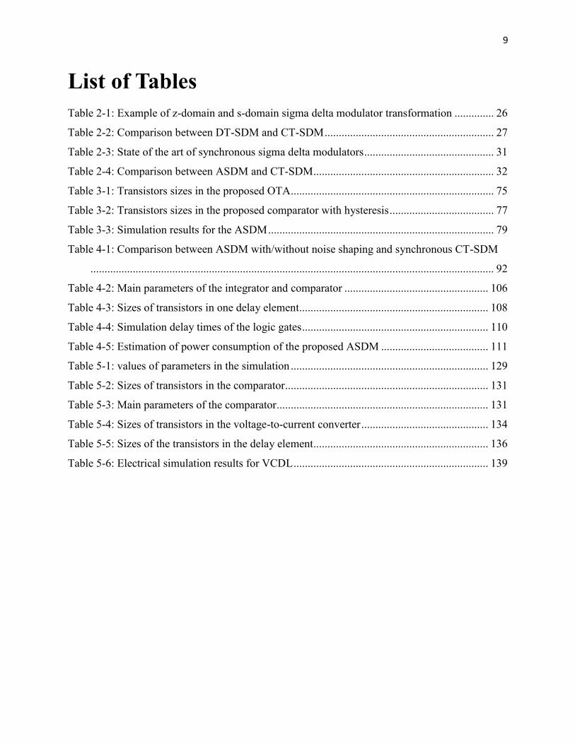
List of Tables
Table 2-1: Example of z-domain and s-domain sigma delta modulator transformation .............. 26
Table 2-2: Comparison between DT-SDM and CT-SDM ............................................................ 27
Table 2-3: State of the art of synchronous sigma delta modulators .............................................. 31
Table 2-4: Comparison between ASDM and CT-SDM ................................................................ 32
Table 3-1: Transistors sizes in the proposed OTA ........................................................................ 75
Table 3-2: Transistors sizes in the proposed comparator with hysteresis ..................................... 77
Table 3-3: Simulation results for the ASDM ................................................................................ 79
Table 4-1: Comparison between ASDM with/without noise shaping and synchronous CT-SDM
............................................................................................................................................... 92
Table 4-2: Main parameters of the integrator and comparator ................................................... 106
Table 4-3: Sizes of transistors in one delay element ................................................................... 108
Table 4-4: Simulation delay times of the logic gates .................................................................. 110
Table 4-5: Estimation of power consumption of the proposed ASDM ...................................... 111
Table 5-1: values of parameters in the simulation ...................................................................... 129
Table 5-2: Sizes of transistors in the comparator ........................................................................ 131
Table 5-3: Main parameters of the comparator ........................................................................... 131
Table 5-4: Sizes of transistors in the voltage-to-current converter ............................................. 134
Table 5-5: Sizes of the transistors in the delay element .............................................................. 136
Table 5-6: Electrical simulation results for VCDL ..................................................................... 139
10
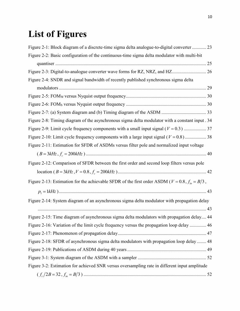
List of Figures
Figure 2-1: Block diagram of a discrete-time sigma delta analogue-to-digital converter ............ 23
Figure 2-2: Basic configuration of the continuous-time sigma delta modulator with multi-bit
quantiser ................................................................................................................................ 25
Figure 2-3: Digital-to-analogue converter wave forms for RZ, NRZ, and HZ ............................. 26
Figure 2-4: SNDR and signal bandwidth of recently published synchronous sigma delta
modulators ............................................................................................................................. 29
Figure 2-5: FOMW versus Nyquist output frequency .................................................................... 30
Figure 2-6: FOMS versus Nyquist output frequency .................................................................... 30
Figure 2-7: (a) System diagram and (b) Timing diagram of the ASDM ...................................... 33
Figure 2-8: Timing diagram of the asynchronous sigma delta modulator with a constant input . 34
Figure 2-9: Limit cycle frequency components with a small input signal ( 0.3V ) ................... 37
Figure 2-10: Limit cycle frequency components with a large input signal ( 0.8V ) .................. 38
Figure 2-11: Estimation for SFDR of ASDMs versus filter pole and normalized input voltage
( 3B kHz , 200cf kHz ) ...................................................................................................... 40
Figure 2-12: Comparison of SFDR between the first order and second loop filters versus pole
location ( 3B kHz , 0.8V , 200cf kHz ) ........................................................................... 42
Figure 2-13: Estimation for the achievable SFDR of the first order ASDM ( 0.8V , 3inf B ,
1 1p kHz ) ............................................................................................................................. 43
Figure 2-14: System diagram of an asynchronous sigma delta modulator with propagation delay
............................................................................................................................................... 43
Figure 2-15: Time diagram of asynchronous sigma delta modulators with propagation delay.... 44
Figure 2-16: Variation of the limit cycle frequency versus the propagation loop delay .............. 46
Figure 2-17: Phenomenon of propagation delay ........................................................................... 47
Figure 2-18: SFDR of asynchronous sigma delta modulators with propagation loop delay ........ 48
Figure 2-19: Publications of ASDM during 40 years ................................................................... 49
Figure 3-1: System diagram of the ASDM with a sampler .......................................................... 52
Figure 3-2: Estimation for achieved SNR versus oversampling rate in different input amplitude
( 2 32cf B , 3inf B ) ........................................................................................................ 52
11
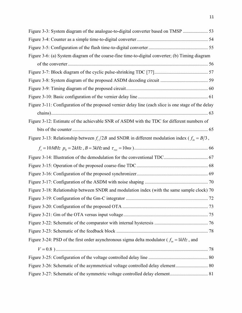
Figure 3-3: System diagram of the analogue-to-digital converter based on TMSP ..................... 53
Figure 3-4: Counter as a simple time-to-digital converter ............................................................ 54
Figure 3-5: Configuration of the flash time-to-digital converter .................................................. 55
Figure 3-6: (a) System diagram of the coarse-fine time-to-digital converter; (b) Timing diagram
of the converter ...................................................................................................................... 56
Figure 3-7: Block diagram of the cyclic pulse-shrinking TDC [77] ............................................. 57
Figure 3-8: System diagram of the proposed ASDM decoding circuit ........................................ 59
Figure 3-9: Timing diagram of the proposed circuit ..................................................................... 60
Figure 3-10: Basic configuration of the vernier delay line ........................................................... 61
Figure 3-11: Configuration of the proposed vernier delay line (each slice is one stage of the delay
chains) .................................................................................................................................... 63
Figure 3-12: Estimate of the achievable SNR of ASDM with the TDC for different numbers of
bits of the counter .................................................................................................................. 65
Figure 3-13: Relationship between 2cf B and SNDR in different modulation index ( 3inf B ,
10sf MHz 0 2p kHz , 3B kHz and 10res ns ) .............................................................. 66
Figure 3-14: Illustration of the demodulation for the conventional TDC ..................................... 67
Figure 3-15: Operation of the proposed coarse-fine TDC ............................................................ 68
Figure 3-16: Configuration of the proposed synchronizer ............................................................ 69
Figure 3-17: Configuration of the ASDM with noise shaping ..................................................... 70
Figure 3-18: Relationship between SNDR and modulation index (with the same sample clock) 70
Figure 3-19: Configuration of the Gm-C integrator ..................................................................... 72
Figure 3-20: Configuration of the proposed OTA ........................................................................ 73
Figure 3-21: Gm of the OTA versus input voltage ....................................................................... 75
Figure 3-22: Schematic of the comparator with internal hysteresis ............................................. 76
Figure 3-23: Schematic of the feedback block ............................................................................. 78
Figure 3-24: PSD of the first order asynchronous sigma delta modulator ( 1inf kHz , and
0.8V ) ................................................................................................................................ 78
Figure 3-25: Configuration of the voltage controlled delay line .................................................. 80
Figure 3-26: Schematic of the asymmetrical voltage controlled delay element ........................... 80
Figure 3-27: Schematic of the symmetric voltage controlled delay element ................................ 81
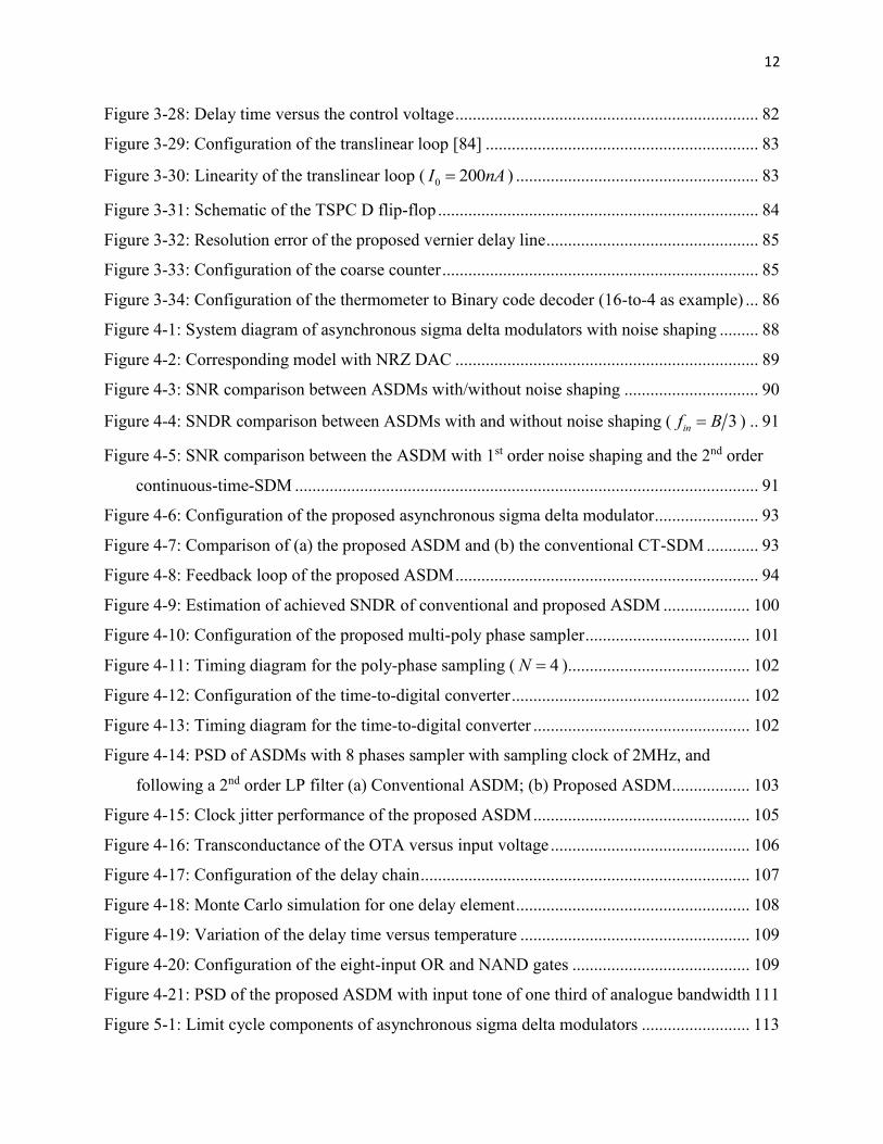
12
Figure 3-28: Delay time versus the control voltage ...................................................................... 82
Figure 3-29: Configuration of the translinear loop [84] ............................................................... 83
Figure 3-30: Linearity of the translinear loop ( 0 200I nA ) ........................................................ 83
Figure 3-31: Schematic of the TSPC D flip-flop .......................................................................... 84
Figure 3-32: Resolution error of the proposed vernier delay line ................................................. 85
Figure 3-33: Configuration of the coarse counter ......................................................................... 85
Figure 3-34: Configuration of the thermometer to Binary code decoder (16-to-4 as example) ... 86
Figure 4-1: System diagram of asynchronous sigma delta modulators with noise shaping ......... 88
Figure 4-2: Corresponding model with NRZ DAC ...................................................................... 89
Figure 4-3: SNR comparison between ASDMs with/without noise shaping ............................... 90
Figure 4-4: SNDR comparison between ASDMs with and without noise shaping ( 3inf B ) .. 91
Figure 4-5: SNR comparison between the ASDM with 1st order noise shaping and the 2nd order
continuous-time-SDM ........................................................................................................... 91
Figure 4-6: Configuration of the proposed asynchronous sigma delta modulator ........................ 93
Figure 4-7: Comparison of (a) the proposed ASDM and (b) the conventional CT-SDM ............ 93
Figure 4-8: Feedback loop of the proposed ASDM ...................................................................... 94
Figure 4-9: Estimation of achieved SNDR of conventional and proposed ASDM .................... 100
Figure 4-10: Configuration of the proposed multi-poly phase sampler ...................................... 101
Figure 4-11: Timing diagram for the poly-phase sampling ( 4N ) .......................................... 102
Figure 4-12: Configuration of the time-to-digital converter ....................................................... 102
Figure 4-13: Timing diagram for the time-to-digital converter .................................................. 102
Figure 4-14: PSD of ASDMs with 8 phases sampler with sampling clock of 2MHz, and
following a 2nd order LP filter (a) Conventional ASDM; (b) Proposed ASDM.................. 103
Figure 4-15: Clock jitter performance of the proposed ASDM .................................................. 105
Figure 4-16: Transconductance of the OTA versus input voltage .............................................. 106
Figure 4-17: Configuration of the delay chain ............................................................................ 107
Figure 4-18: Monte Carlo simulation for one delay element ...................................................... 108
Figure 4-19: Variation of the delay time versus temperature ..................................................... 109
Figure 4-20: Configuration of the eight-input OR and NAND gates ......................................... 109
Figure 4-21: PSD of the proposed ASDM with input tone of one third of analogue bandwidth 111
Figure 5-1: Limit cycle components of asynchronous sigma delta modulators ......................... 113
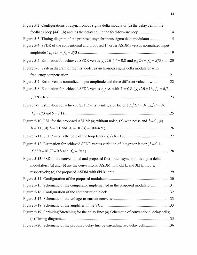
13
Figure 5-2: Configurations of asynchronous sigma delta modulator (a) the delay cell in the
feedback loop [44]; (b) and (c) the delay cell in the feed-forward loop .............................. 114
Figure 5-3: Timing diagram of the proposed asynchronous sigma delta modulator .................. 115
Figure 5-4: SFDR of the conventional and proposed 1st order ASDMs versus normalized input
amplitude ( 0 2 3inp f B ) ........................................................................................... 119
Figure 5-5: Estimation for achieved SFDR versus 2cf B ( 0.8V and 1 2 3inp f B ) .... 120
Figure 5-6: System diagram of the first-order asynchronous sigma delta modulator with
frequency compensation ...................................................................................................... 121
Figure 5-7: Errors versus normalized input amplitude and three different value of .............. 122
Figure 5-8: Estimation for achieved SFDR versus 0pt t with 0.8V ( 2 16cf B , 3inf B ,
1 1 6p B ) ......................................................................................................................... 123
Figure 5-9: Estimation for achieved SFDR versus integrator factor ( 2 16cf B , 0 1 6p B
3inf B and 0.1b ) .......................................................................................................... 125
Figure 5-10: PSD for the proposed ASDM: (a) without noise, (b) with noise and 0b , (c)
0.1b , (d) 0.1b and 0 10A ( 100sf MHz ) ................................................................ 126
Figure 5-11: SFDR versus the pole of the loop filter ( 2 16cf B ) ........................................... 127
Figure 5-12: Estimation for achieved SFDR versus variation of integrator factor ( 0.1b ,
2 16cf B , 0.8V and 3inf B ) ................................................................................... 128
Figure 5-13: PSD of the conventional and proposed first-order asynchronous sigma delta
modulators: (a) and (b) are the conventional ASDM with 6kHz and 3kHz inputs,
respectively; (c) the proposed ASDM with 6kHz input ...................................................... 129
Figure 5-14: Configuration of the proposed modulator .............................................................. 130
Figure 5-15: Schematic of the comparator implemented in the proposed modulator ................. 131
Figure 5-16: Configuration of the compensation block .............................................................. 132
Figure 5-17: Schematic of the voltage-to-current converter ....................................................... 133
Figure 5-18: Schematic of the amplifier in the VCC .................................................................. 133
Figure 5-19: Shrinking/Stretching for the delay line: (a) Schematic of conventional delay cells;
(b) Timing diagram .............................................................................................................. 135
Figure 5-20: Schematic of the proposed delay line by cascading two delay cells ...................... 136
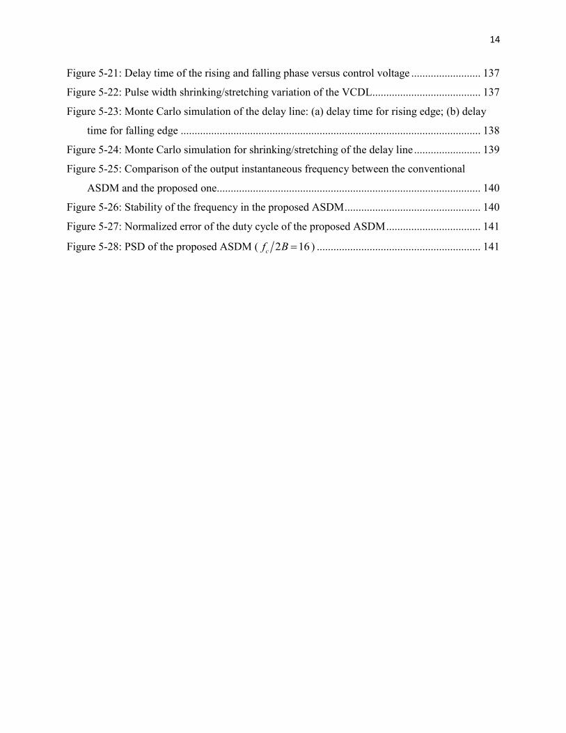
14
Figure 5-21: Delay time of the rising and falling phase versus control voltage ......................... 137
Figure 5-22: Pulse width shrinking/stretching variation of the VCDL....................................... 137
Figure 5-23: Monte Carlo simulation of the delay line: (a) delay time for rising edge; (b) delay
time for falling edge ............................................................................................................ 138
Figure 5-24: Monte Carlo simulation for shrinking/stretching of the delay line ........................ 139
Figure 5-25: Comparison of the output instantaneous frequency between the conventional
ASDM and the proposed one............................................................................................... 140
Figure 5-26: Stability of the frequency in the proposed ASDM ................................................. 140
Figure 5-27: Normalized error of the duty cycle of the proposed ASDM .................................. 141
Figure 5-28: PSD of the proposed ASDM ( 2 16cf B ) ........................................................... 141

15
List of Symbols
A list of the major symbols, notations and abbreviations with their definitions are as follows:
Absolute value
Convolution
Re Real part of a complex number
Im Imaginary part of a complex number
FT Fourier transfer function
B Signal bandwidth
0f Output instantaneous frequency
cf Limit cycle frequency
sT Period of sample clock
refT Period of reference clock
Input signal frequency
Delay time of the delay line
DRT Dynamic range of the delay line
0A Open loop gain
Propagation delay time
1e / Quantisation error
L Order of the loop filter
V Normalized input signal amplitude
Duty cycle of the data signal
F Carrier-to-bandwidth ratio
NC Output of the coarse measurement
NF Output of the fine measurement
b Hysteresis of the comparator
p Pole frequency of the loop filter
16
1k RC Integration gain
3 /HD3 The third order distortion
gm Transconductance
fbV Amplitude of the feedback signal
biasI Bias current
I Current
controlV Control voltage of the delay line
oxC Oxide capacitance of the gate-to-body per unit area
n Electron mobility in the induced n channel
p Electron mobility in the induced p channel
Minimum quantisation step
0t Delay time of the delay line
SC Switch capacitor
STF Signal transfer function
NTF Noise transfer function
SNR Signal-to-noise ratio
SQNR Signal-to-quantisation noise ratio
SFDR Spurious-free dynamic range
SNDR Signal-to-noise and distortion ratio
OSR Oversampling ratio
ADC Analogue-to-digital converter
DAC Digital-to-analogue converter
SDM Sigma delta modulator
PWM Pulse width modulator
DT SDM Discrete-time sigma delta modulator
CT SDM Continuous-time sigma delta modulator
ASDM Asynchronous sigma delta modulator
NTZ Non-return-to-zero
RZ Return-to-zero
17
HZ Hold-return-to-zero
VDL Vernier delay line
VCDL Voltage controlled delay line
TDC Time-to-digital converter
TL Translinear loop
DTC Tine-to-digital converter
PLL Phase locked loop
DLL Delay locked loop
LPF Low pass filter
TMSP Time-mode signal processing
INL Integral non-linearity
DNL Differential non-linearity
LSB Least significant bit
OTA Operational transconductance amplifier
Gm-C Transconductor-capacitor circuit
18
Introduction
1.1 Motivation
Despite its long history, the sigma delta modulator remains one of the most popular data converter
circuits. Conventionally, sigma delta modulators are widely implemented in low-speed, high-
resolution applications. Low power consumption is a particularly important feature in portable
applications, leading to long battery life. Consequently, power-efficient architectures such as
continuous-time sigma delta modulators have been attracted more attention in recent years.
Continuous-time sigma delta modulators use a cascade of several loop filters to establish a high
order noise shaping, so as to realize a high resolution. A single-bit digital-to-time converter (DAC)
inherently linear, is implemented in the feedback loop for reasons of circuit simplicity and low
power consumption. However, the single-bit quantizer in the forward path will raise stability issues
in high order modulators [1]. To solve this issue, a multi-bit internal quantizer is often used to
obtain sufficient gain for implementing a stable sigma delta loop filter. This creates another issue:
An equivalent high resolution DAC is required in the feedback loop, which increases the
complexity of the modulator and the power consumption.
Continuous-time sigma delta modulators require a high sampling frequency to obtain an equivalent
over-sampling ratio, in order to improve performance. High sampling frequency not only means
increased power dissipation of the clock and sampler, but also increases the design and simulation
time and the power consumption of the wideband loop and decimation filters. All this limits sigma
delta modulators to ultra-low power applications, such as biomedical and environmental sensors.
Other design issues around continuous-time sigma delta modulators include propagation delay and
sensitivity to clock jitter. Propagation delay undermines dynamic stability and introduces the need
for compensation.
19
In fact, there does exist another type of sigma delta modulators, named asynchronous sigma delta
modulators (ASDM), which has potential properties to solve this issue. ASDMs can be considered
as a special type of continuous-time sigma delta modulators. Unfortunately, in current CMOS
technology, ASDMs are difficult to implement in data conversion, because of some critical issues.
Most significant drawback is the absence of effective circuit to digitise the modulated signal. Other
issues which can be resolved including the signal bandwidth which is limited by the limit cycle
components and lacking of shaping for quantisation errors. This thesis presents solutions to solve
these issues.
1.2 Objectives
This thesis presents studies of the asynchronous sigma delta modulator and proposes solutions to
their limitations.
1. Improve a decoding scheme for ASDMs. In the first instance, I noticed that conventional
decoding schemes for asynchronous sigma delta modulators limit input dynamic range of
modulators, and always requires a high speed sampling clock. This is because conventional
decoding schemes can only measure the time interval not the duty cycle of the square wave,
and they always use a fast sample to digital the location of the time interval rather than its
exact the time value. In order to obtain the duty cycle, two decoding schemes are required
to measure both the pulse width and the period, which doubles the chip area and power
dissipation. To solve this issue, I introduce a novel decoding scheme for asynchronous
sigma delta modulators, which can convert the duty cycle of modulated square wave into
digital signals directly. The proposed decoding scheme is realized by a special coarse-fine
time-to-digital converter (TDC), and it can measure the duty cycle of the data signal
without knowing its instantaneous period.
2. Improve the architecture of ASDMs to introduce noise shaping. I found that the
conventional architecture of asynchronous sigma delta modulators with noise shaping with
additional loop filter and feedback loop is not efficient. Because the loop filter in the
ASDM does not contribute to shape the quantisation errors. And it requires a high
resolution digital-to-analogue converter (DAC) in the feedback loop, which increases the
design challenge and the complexity of the circuit. Compared with the same system order
20
synchronous-time sigma delta modulator, the conventional architecture has poorer
performance.
3. Improve the architecture of ASDMs to minimize effects of limit cycle components. Finally,
I noticed that the limit cycle components of asynchronous sigma delta modulators
significantly limit the signal bandwidth of modulators, and it also requires a powerful
decimation filter to supply a high attenuation for out-band components. This issue makes
ASDM difficult to implement. To overcome this issue, another architecture of ASDMs is
implemented, where the limit cycle frequency is determined by the delay time of a delay
cell. It give an opportunity to stable the frequency of the output by controlling the delay
time of the delay cell. The proposed ASDM works as an ideal pulse width modulator
(PWM), which increases design space of decoding circuits, and reduces the requirement of
the decimation.
1.3 Outline of this thesis
The thesis is organized in 6 chapters, including the present one. A brief summary of each chapter
is given below.
Chapter 2 provides a brief literature review of sigma delta modulators in past five years. A detailed
system analysis of asynchronous sigma delta modulators is presented, including fundamental
analysis, noise performance and non-idealises.
Chapter 3 presents the implementation of an asynchronous sigma delta modulator with a novel
decoding circuit. It discusses the issues of conventional decoding circuits, and introduces a new
decoding methodology to overcome these issues. It also presents the architecture of the proposed
modulator and decoding circuit in some details, along with simulation results.
Chapter 4 introduces a novel architecture of asynchronous sigma delta modulators with noise
shaping. It solves the issues of conventional architectures of asynchronous sigma delta modulators
with noise shaping, and presents the details of system analysis and circuits design. The results of
the system analysis are illustrated by transistor level simulation results of modulator circuits.
21
Chapter 5 presents improvements of the asynchronous sigma delta modulator leading to a constant
output frequency. This is achieved by the introduction of a compensation block. The methodology
of frequency compensation is presented in detail. This chapter concludes with transistor-level
simulation results of the entire modulator circuits in an AMS 0.35 m CMOS process.
Chapter 6 presents some concluding remarks, outlines the limitations of the thesis and discusses
some potential directions for future research.
22
Sigma Delta Modulation Fundamentals
1.4 Introduction
Analogue-to-Digital converters (ADCs) are key building blocks in electronic systems, including
as audio, communication, industry measurement and sensor interfaces. Together with digital-to-
analogue converters (DACs), they interface analogue real world signals to the digital signal
processing system. Application requirements, such as speed, resolution and power consumption,
dictate specific ADC architectures to optimise trade-off between power, speed and performance.
The sigma delta analogue-to-digital converters are preferred in high-resolution, low-speed
applications. Sigma delta converters use oversampling, error processing, and feedback to improve
the resolution of the quantiser. In other words many samples of the input signal taken at a high rate
are used to produce an output signal at the Nyquist rate. Sigma delta converters are feedback
devices operating in closed-loop mode; this makes them tolerant to some analogue imperfections,
including offset and mismatch. Additionally, signal processing in a sigma delta analogue-to-digital
converter is partitioned between analogue and digital sub-sections; analogue filtering is employed
for quantisation error rejection from the signal band, while digital filtering is used to increase the
effective resolution by eliminating the out of band quantisation noise [2]. The single-bit sigma
delta converter is inherently monotonic and requires no laser trimming [1]. It also lends itself to
low cost CMOS foundry processes because of the digitally intensive nature of the architecture.
This chapter will present the fundamentals of both synchronous and asynchronous sigma delta
modulators.
1.5 Synchronous sigma delta modulators
1.5.1 Discrete-time sigma delta modulator
Discrete-time sigma delta analogue-to-digital converters make use of two basic ideas:
oversampling and noise shaping, to decrease the quantisation error power within the signal band
and increase the resolution of the conversion. The basic system diagram of a discrete-time sigma
delta analogue-to-digital converter is shown in Fig. 2-1. It includes three basic components: an
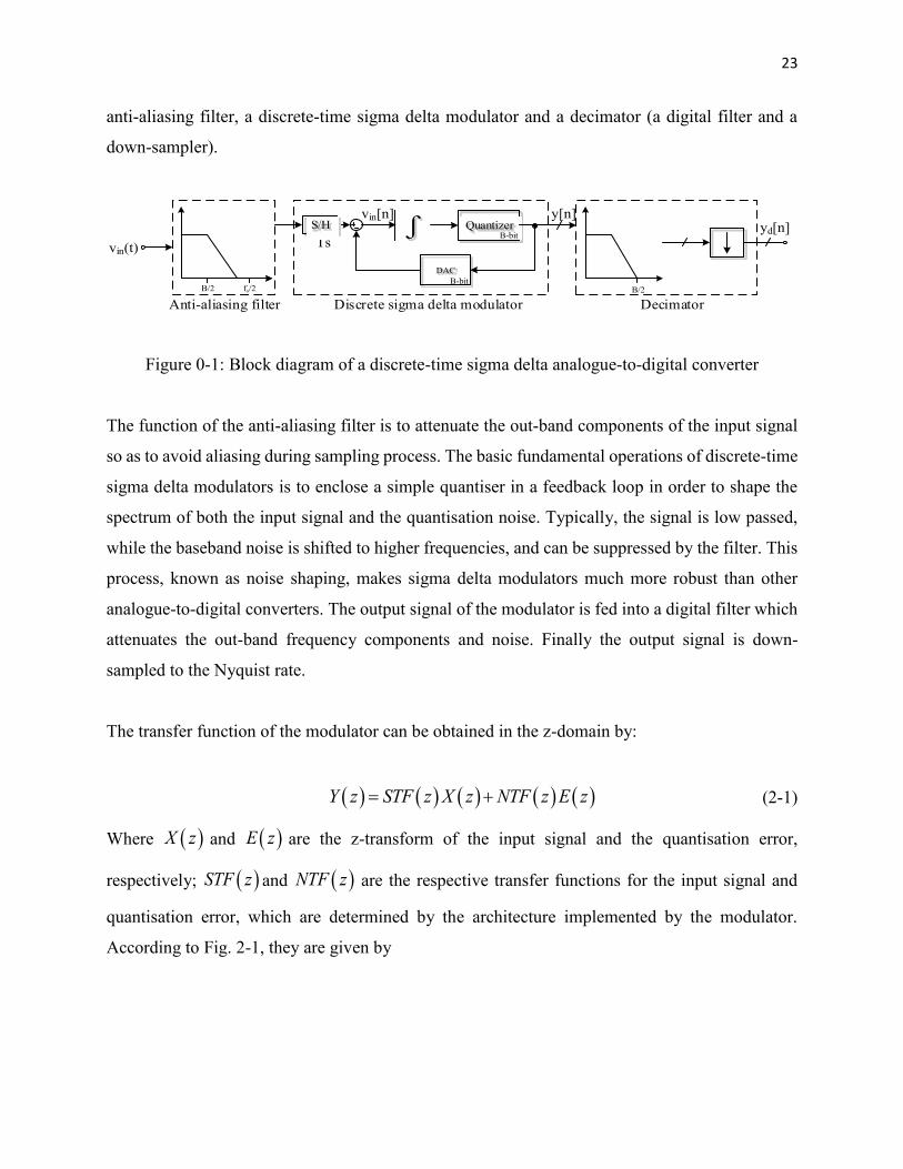
23
anti-aliasing filter, a discrete-time sigma delta modulator and a decimator (a digital filter and a
down-sampler).
fs/2B/2
Anti-aliasing filter
ʃvin(t)
QuantizerB-bit
Ts
y[n]
DAC
B-bit
vin[n]S/H
Discrete sigma delta modulator
B/2
yd[n]
Decimator
Figure 0-1: Block diagram of a discrete-time sigma delta analogue-to-digital converter
The function of the anti-aliasing filter is to attenuate the out-band components of the input signal
so as to avoid aliasing during sampling process. The basic fundamental operations of discrete-time
sigma delta modulators is to enclose a simple quantiser in a feedback loop in order to shape the
spectrum of both the input signal and the quantisation noise. Typically, the signal is low passed,
while the baseband noise is shifted to higher frequencies, and can be suppressed by the filter. This
process, known as noise shaping, makes sigma delta modulators much more robust than other
analogue-to-digital converters. The output signal of the modulator is fed into a digital filter which
attenuates the out-band frequency components and noise. Finally the output signal is down-
sampled to the Nyquist rate.
The transfer function of the modulator can be obtained in the z-domain by:
Y z STF z X z NTF z E z (2-1)
Where X z and E z are the z-transform of the input signal and the quantisation error,
respectively; STF z and NTF z are the respective transfer functions for the input signal and
quantisation error, which are determined by the architecture implemented by the modulator.
According to Fig. 2-1, they are given by
24
1
1
1
H zSTF z
H z
NTF zH z
(2-2)
Where H z is the loop filter transfer function. By implementing a simple ideal loop filter:
1
11
zH z
z
(2-3)
Eq. (2-1) can be extended to an thL order system yields:
1L LY z z X z z E z (2-4)
Ideally, the dynamic range of the thL order sigma delta modulator is:
10 102
2 16.02 1.76 10log 2 1 10log ( )
L
LDR N L OSR
(2-5)
Where 2sOSR f B is the oversampling ratio; N is the bit of the quantiser.
The dynamic range of the modulator will, in general, be limited by quantisation noise and circuit
imperfections.
1.5.2 Continuous-time sigma delta modulator
The first recognizable sigma delta modulator, introduced in 1962, was actually implemented as a
continuous-time circuit [3]. However, because of the excellent performance of switched-capacitor
circuits, most sigma delta modulators are implemented as the discrete-time mode. Switched-
capacitor sigma delta modulators are still very popular in middle frequency applications because
of their insensitivity to signal waveform. As the time constants of switched-capacitor integrators
scale with sampling frequency, switched capacitor modulator circuits allow for greater system
flexibility [4].
25
However, continuous-time sigma delta modulators are attracting attention once again thanks to the
increasing demand for lower power circuits. Continuous time modulators have a unique benefit,
namely the inherent anti-aliasing filtering offered by the continuous-time loop filter. Continuous-
time loop filters are much faster than their discrete-time counterparts, making continuous-time
sigma delta modulators popular in high-speed analogue-to-digital converters. The configuration of
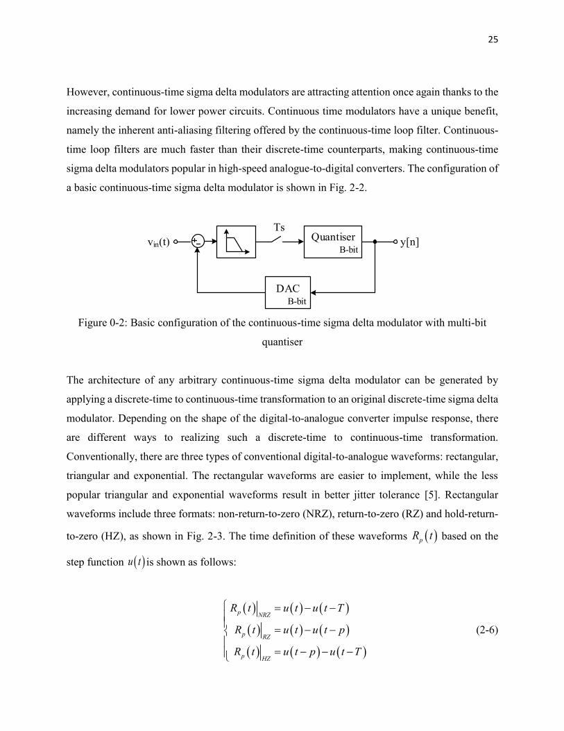
a basic continuous-time sigma delta modulator is shown in Fig. 2-2.
vin(t)B-bit
Ts
y[n]
B-bit
Quantiser
DAC
Figure 0-2: Basic configuration of the continuous-time sigma delta modulator with multi-bit
quantiser
The architecture of any arbitrary continuous-time sigma delta modulator can be generated by
applying a discrete-time to continuous-time transformation to an original discrete-time sigma delta
modulator. Depending on the shape of the digital-to-analogue converter impulse response, there
are different ways to realizing such a discrete-time to continuous-time transformation.
Conventionally, there are three types of conventional digital-to-analogue waveforms: rectangular,
triangular and exponential. The rectangular waveforms are easier to implement, while the less
popular triangular and exponential waveforms result in better jitter tolerance [5]. Rectangular
waveforms include three formats: non-return-to-zero (NRZ), return-to-zero (RZ) and hold-return-
to-zero (HZ), as shown in Fig. 2-3. The time definition of these waveforms pR t based on the
step function u t is shown as follows:
p NRZ
p RZ
p HZ
R t u t u t T
R t u t u t p
R t u t p u t T
(2-6)
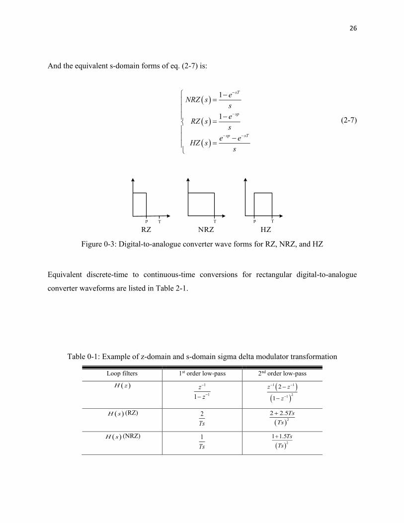
26
And the equivalent s-domain forms of eq. (2-7) is:
1
1
sT
sp
sp sT
eNRZ s
s
eRZ s
s
e eHZ s
s
(2-7)
T T Tpp
RZ NRZ HZ
Figure 0-3: Digital-to-analogue converter wave forms for RZ, NRZ, and HZ
Equivalent discrete-time to continuous-time conversions for rectangular digital-to-analogue
converter waveforms are listed in Table 2-1.
Table 0-1: Example of z-domain and s-domain sigma delta modulator transformation
Loop filters 1st order low-pass 2nd order low-pass
H z 1
11
z
z
1 1
21
2
1
z z
z
H s (RZ) 2
Ts
2
2 2.5Ts
Ts
H s (NRZ) 1
Ts
2
1 1.5Ts
Ts
27
Continuous-time sigma delta modulators have several critical limitations. The first one is related
to the excess loop delay. In practice, there exists a certain delay between the quantiser sampling
event and the DAC output, caused by the imperfection of circuits implemented in the modulator,
such as the finite open loop gain and bandwidth of the loop filter, the propagation delay time in
comparator, etc. This delay cause instability of the modulator loop. In intuitive terms, if the DAC
feedback waveform is not contained in one sampling period due to the excess loop delay, the
effective order of the loop filter is larger than desired; the loop poles move towards the unite circle,
and the modulator stability becomes poor. Moreover, the excess loop delay can elevate the
quantisation noise floor by degrading the noise transfer function at low-frequencies.
Continuous time sigma delta modulators are also more sensitive to the clock jitter than discrete-
time sigma delta modulators; the internal clock not only controls the comparison instant, but also
controls the rising and falling edges of the digital-to-analogue converter output. As a result, clock
jitter errors are directly added to the input signal. The effect of clock jitter in continuous-time
sigma delta modulators has been extensively analysed in the literatures [6-8]. K. Reddy and S.
Pavan’s work showed that the jitter induced noise in modulators with NRZ feedback is
predominantly determined by the out-band behaviour of the NTF, thus more aggressive noise
shaping exacerbates the jitter sensitivity.
Many authors have presented solutions to these issues. However, they all focus on the detailed
circuit design and some compensation techniques [9-12], which increase the challenge of design,
complex of the circuits, and the power dissipation as well. The comparison between DT-SDM and
CT-SDM is shown in Table 2-2.
Table 0-2: Comparison between DT-SDM and CT-SDM
DT-SDM CT-SDM
Common Synchronous modulator
Noise shaping and over-sampling
High order system (at least 2nd order system)
Advantages High resolution
Developed technology
Inherent anti-aliasing filter
High conversion speed
Disadvantages Require pre anti-aliasing filter
Low conversion speed
Sensitive to clock jitter
Excess loop delay (instability)
28
Instability (high order system)
1.6 State of the art for the synchronous sigma delta modulator
With the exception of a few milestone works, referenced for completeness, a literature survey on
recently published synchronous sigma delta modulators is summarized in Table 2-2. Discrete-time
sigma delta modulators are implemented by switched-capacitor or switched-current techniques;
continuous-time sigma delta modulators are often realized by active-RC or Gm-C techniques. The
signal bandwidth, signal-to-noise ratio (SNR), signal-to-noise and distortion ratio (SNDR), and
power consumption are key performance metrics that can be used for comparing different designs.
Low pass sigma delta modulators are evaluated by two figures-of-merits, namely:
2 2W ENOB
PFOM
B
(2-8)
10logS
BFOM SNDR
p
(2-9)
FOMW emphasizes power consumption, whereas FOMS emphasizes resolution. Better
performance of sigma delta modulators is indicated by smaller FOMw and larger FOMS values.
The data in Table 2-3 clearly shows that current trend is towards continuous-time sigma delta
modulators; an increasing number of published sigma delta modulators are based on the
continuous-time approach. In order to form an idea of current design trends, and to compare the
potentials of discrete-time and continuous-time implementation, a survey of design approaches is
presented here. The survey covers publications in the IEEE International Solid State Circuits
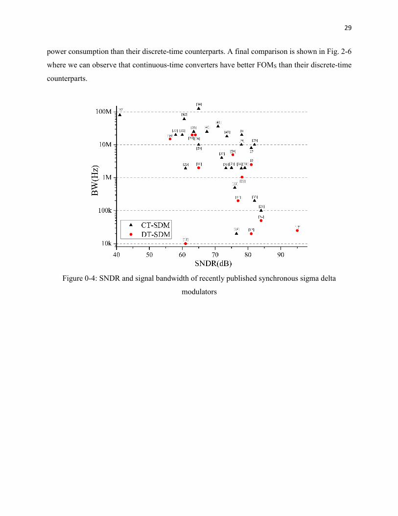
Conference (ISSCC) and the IEEE VLSI Conference from 2008 to 2013. Fig. 2-4 shows the
Signal-to-Noise-and Distortion (SNDR) versus signal bandwidth of discrete-time and continuous-
time implementations. Continuous-time circuits mostly cover the high frequency applications. The
higher dynamic range is mostly occupied by low signal bandwidth, discrete-time implementations.
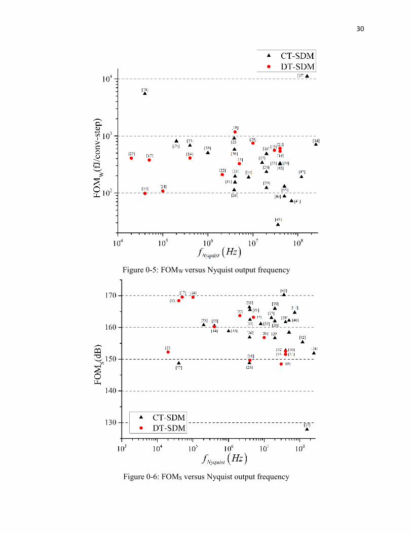
A survey of power consumption versus Nyquist output frequency is presented in Fig. 2-5. Note
that the continuous-time implementations, even in high frequency applications, still show a lower
29
power consumption than their discrete-time counterparts. A final comparison is shown in Fig. 2-6
where we can observe that continuous-time converters have better FOMS than their discrete-time
counterparts.
Figure 0-4: SNDR and signal bandwidth of recently published synchronous sigma delta
modulators
30
Figure 0-5: FOMW versus Nyquist output frequency
Figure 0-6: FOMS versus Nyquist output frequency
31
Table 0-3: State of the art of synchronous sigma delta modulators
Discrete-time sigma delta modulators
Year Technology
(um)
BW
(Hz)
Fs
(Hz)
OSR SNDR
(dB)
Power
(mW)
FOMW
(fJ/conv-step)
FOMS
(dB)
2008[13] 0.18 2.00E+4 4.00E+6 100 81.0 3.60E-2 98.1 168.4
2008[14] 0.065 2.00E+5 1.50E+8 375 77.0 9.50E-1 410.5 160.2
2008[15] 0.18 2.50E+6 6.00E+7 12 83.0 15.0 327.1 163.2
2008[16] 0.09 2.00E+7 4.20E+8 11 72.0 27.9 538.6 152.6
2008[17] 0.18 2.50E+4 5.00E+6 100 100.0 8.70E-1 378.5 169.6
2009[18] 0.09 2.00E+6 3.20E+8 80 65 6.83 1175.0 149.7
2009[19] 0.045 1.50E+7 1.50E+9 50 56.3 9.00 562.1 148.5
2009[20] 0.18 5.00E+6 8.00E+7 8 75.4 36.0 748.1 156.8
2011[21] 0.032 2.00E+7 4.00E+8 10 63.0 28.0 606.4 151.5
2011[22] 0.18 1.04E+6 5.00E+7 24 78.2 2.90 209.5 163.8
2011[23] 0.13 1.00E+4 1.40E+6 70 61.0 7.50E-3 409.0 152.2
2011[24] 0.18 5.00E+4 1.60E+6 16 84.0 1.40E-1 108.1 169.5
Continuous-time sigma delta modulators
Year Technology
(um)
BW
(Hz)
Fs
(Hz)
OSR SNDR
(dB)
Power
(mW)
FOMW
(fJ/conv-step)
FOMS
(dB)
2008[25] 0.065 1.00E+5 2.60E+7 130 84.0 2.10 810.5 160.8
2008[25] 0.065 1.92E+6 6.24E+7 16 61.0 3.20 908.9 148.8
2008[26] 0.18 1.00E+7 6.40E+8 32 82.0 100 485.9 162.0
2008[27] 0.065 8.00E+6 2.56E+8 16 81.0 50.0 340.8 163.0
2008[28] 0.045 2.00E+4 1.20E+7 300 76.5 1.20 5492.2 148.7
2009[29] 0.09 1.00E+7 6.40E+8 32 65.0 6.80 234.0 156.7
2009[30] 0.13 2.00E+7 9.00E+8 23 78.1 87.0 331.2 161.7
2009[31] 0.065 2.00E+6 1.28E+8 32 79.1 4.52 153.9 165.5
2009[32] 0.065 2.00E+7 2.50E+8 6 60.0 10.5 321.2 152.8
2010[33]
GSM mode
0.09 2.00E+5 5.12E+7 128 82.0 2.80 680.3 160.5
2010[33]
BT mode
0.09 5.00E+5 9.60E+7 96 78 2.60 504.2 158.8
2010[33]
UMTS mode
0.09 2.00E+6 1.28E+8 32 75 3.60 195.8 162.4
32
2010[33]
DVB-H mode
0.09 4.00E+6 1.92E+8 24 72 4.90 188.3 161.1
2010[33]
WLAN mode
0.09 2.00E+7 6.40E+8 16 58 8.50 327.4 151.7
2011[34] 0.045 1.25E+8 4.00E+9 16 65.0 256 704.7 151.9
2011[35] 0.09 2.50E+7 5.00E+8 10 63.5 8.00 130.9 158.4
2011[36] 0.065 1.95E+6 1.25E+8 32 73.3 8.55 580.2 156.9
2011[37] 0.04 8.00E+7 8.88E+9 56 41.0 164 11148.1 127.9
2011[38] 0.04 1.92E+6 2.46E+8 64 78.0 2.80 112.3 166.4
2012[39] 0.09 1.00E+7 6.00E+8 30 78.0 16.0 123.2 166.0
2012[40] 0.09 2.50E+7 5.00E+8 10 67.5 8.50 87.7 162.2
2012[41] 0.09 3.60E+7 3.60E+9 50 70.9 15.0 72.7 164.7
2012[42] 0.045 6.00E+7 6.00E+9 50 60.6 20.0 190.4 155.4
2013[43] 0.028 1.80E+7 6.40E+8 18 73.6 3.90 27.7 170.2
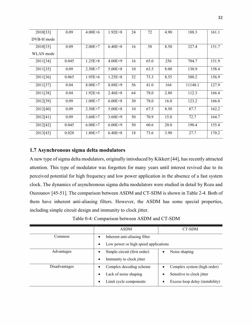
1.7 Asynchronous sigma delta modulators
A new type of sigma delta modulators, originally introduced by Kikkert [44], has recently attracted
attention. This type of modulator was forgotten for many years until interest revived due to its
perceived potential for high frequency and low power application in the absence of a fast system
clock. The dynamics of asynchronous sigma delta modulators were studied in detail by Roza and
Ouzounov [45-51]. The comparison between ASDM and CT-SDM is shown in Table 2-4. Both of
them have inherent anti-aliasing filters. However, the ASDM has some special properties,
including simple circuit design and immunity to clock jitter.
Table 0-4: Comparison between ASDM and CT-SDM
ASDM CT-SDM
Common Inherent anti-aliasing filter
Low power or high speed applications
Advantages Simple circuit (first order)
Immunity to clock jitter
Noise shaping
Disadvantages Complex decoding scheme
Lack of noise shaping
Limit cycle components
Complex system (high order)
Sensitive to clock jitter
Excess loop delay (instability)
33
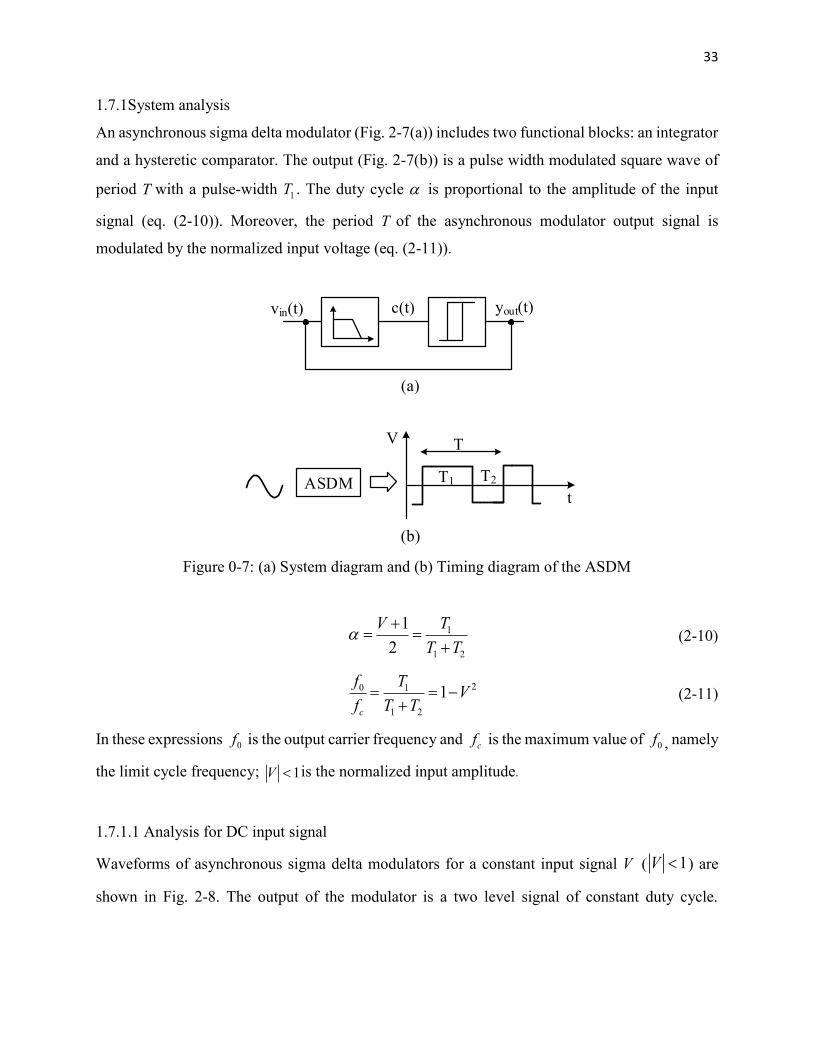
1.7.1System analysis
An asynchronous sigma delta modulator (Fig. 2-7(a)) includes two functional blocks: an integrator
and a hysteretic comparator. The output (Fig. 2-7(b)) is a pulse width modulated square wave of
period T with a pulse-width 1T . The duty cycle is proportional to the amplitude of the input
signal (eq. (2-10)). Moreover, the period T of the asynchronous modulator output signal is
modulated by the normalized input voltage (eq. (2-11)).
vin(t)
(a)
(b)
t
V T
T1 T2
yout(t)c(t)
ASDM
Figure 0-7: (a) System diagram and (b) Timing diagram of the ASDM
1
1 2
1
2
TV
T T
(2-10)
20 1
1 2
1c
f TV
f T T
(2-11)
In these expressions 0f is the output carrier frequency and cf
is the maximum value of 0f , namely
the limit cycle frequency; 1V is the normalized input amplitude.
1.7.1.1 Analysis for DC input signal
Waveforms of asynchronous sigma delta modulators for a constant input signal V ( 1V ) are
shown in Fig. 2-8. The output of the modulator is a two level signal of constant duty cycle.
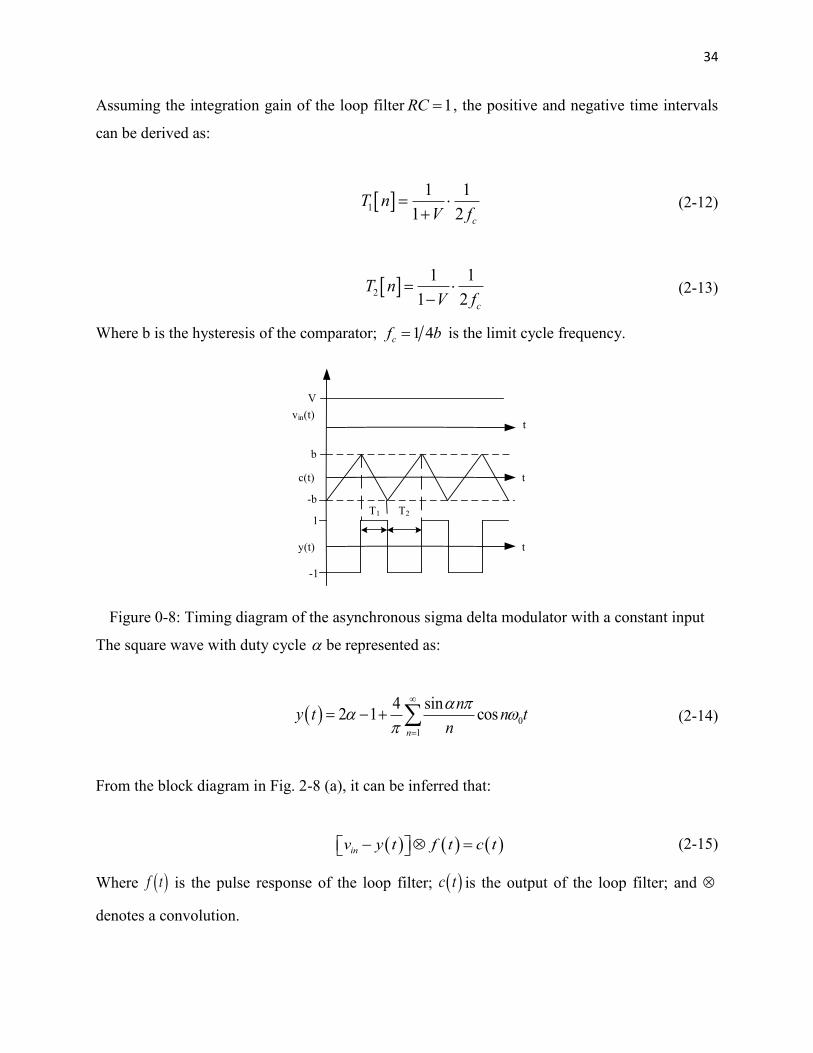
34
Assuming the integration gain of the loop filter 1RC , the positive and negative time intervals
can be derived as:
1
1 1
1 2 c
T nV f
(2-12)
2
1 1
1 2 c
T nV f
(2-13)
Where b is the hysteresis of the comparator; 1 4cf b is the limit cycle frequency.
1
b
-b
-1
t
t
T1 T2
c(t)
y(t)
tvin(t)
V
Figure 0-8: Timing diagram of the asynchronous sigma delta modulator with a constant input
The square wave with duty cycle be represented as:
0
1
4 sin2 1 cos
n
ny t n t
n
(2-14)
From the block diagram in Fig. 2-8 (a), it can be inferred that:
inv y t f t c t (2-15)
Where f t is the pulse response of the loop filter; c t is the output of the loop filter; and
denotes a convolution.
35
According to Appendix I, c t can be derived as:
0 0 0 0
1
4 sin2 1 0 Re cos Im sin
n
nc t V F F n n t F n n t
n
(2-16)
Based on the boundary conditions:
11 1 1 1 2
12 2 2 1 2
1, ,2
1, ,2
Ty t c t b t k T T
Ty t c t b t k T T
(2-17)
Addition and subtraction of eq. (2-16) based on conditions results in:
10 0
1
2 10
0
1
4 sin2 1 0 Re cos
2
sin2 Im
4
n
n
TnV F F n n
n
Tn
bF n
n
(2-18)
Assuming the loop filter is an ideal integrator with a transfer function of:
1
Fj
(2-19)
After a little algebraic manipulation we get the expressions for the frequency and duty cycle of the
output signal:
2
0
1
2
1c
V
f f V
(2-20)
36
When a zero input is applied, the output of the asynchronous sigma delta modulator is a square
wave with duty cycle of 50%. The frequency of the output then reaches its maximum value named
as the limit cycle frequency.
1.7.1.2 Analysis for a sinusoidal input signal
With a non-trivial input the system becomes complex to analyse. However, if we assume the input
signal is slow changing, in other words, the output instantaneous frequency of the modulator is
much higher than that the input signal, 1c inf f , the expression of eq. (2-16) is still valid in one
period, 1m mT t T .
We assume that the input is cosinv V t , with 1V , normalized to the power supply. Here we
rewrite the input signal as 1
cosin m m
m
v T V T
. In one period 1m mT t T , the input signal can
be considered to be constant. When 1 0m mT T , it becomes the original sine wave. In this case,
eq. (2-14) can be rewritten as:
2 2
1 1 1
1 cossin
cos 24 2cos cos 1
2
m
mm c
m m n
V Tn
V V Ty t V T n dt
n
(2-21)
By inserting the boundary conditions eq. (2-15), and based on eq. (I-11) in Appendix I the
following equations can be derived:
0
1
2
0
1
2 sin 2cos 2 1 Re Re
sinIm
4
m
n
n
nV T F F n
n
n bF n
n
(2-22)
We are particularly interested in the first harmonic band (n=1) of y t :
22
1
1
cos4cos cos 1 sin 2
2 2 4
m cc m
m s
V T VVy t t T
(2-23)
37
Here we implement the Jacobi-Anger expansion (Appendix I) to rewrite eq. (2-23) as:
2
2 2201 2
4Re
2 4
in t im ti m t
n m
n m
Vy t J V J e e e
(2-24)
It is clear from eq. (2-24), that the amplitudes and frequencies of the Bessel components are a
function of both the amplitude and frequency of the input signal and the limit cycle frequency as
well. The high-frequency components are tones at frequencies 0 2 inf k f , where k is an integer
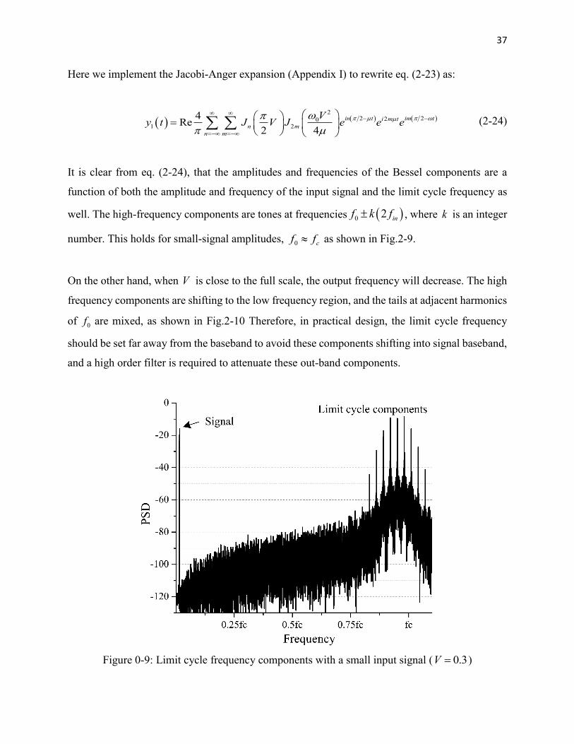
number. This holds for small-signal amplitudes, 0 cf f as shown in Fig.2-9.
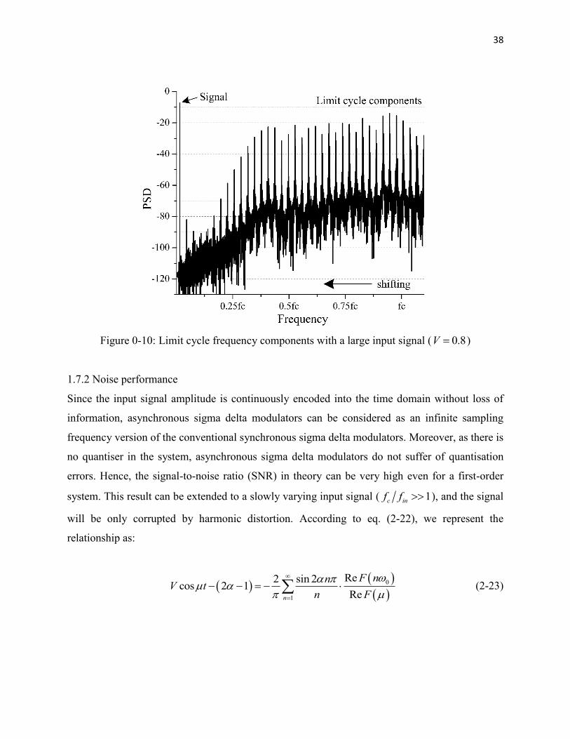
On the other hand, when V is close to the full scale, the output frequency will decrease. The high
frequency components are shifting to the low frequency region, and the tails at adjacent harmonics
of 0f are mixed, as shown in Fig.2-10 Therefore, in practical design, the limit cycle frequency
should be set far away from the baseband to avoid these components shifting into signal baseband,
and a high order filter is required to attenuate these out-band components.
Figure 0-9: Limit cycle frequency components with a small input signal ( 0.3V )
38
Figure 0-10: Limit cycle frequency components with a large input signal ( 0.8V )
1.7.2 Noise performance
Since the input signal amplitude is continuously encoded into the time domain without loss of
information, asynchronous sigma delta modulators can be considered as an infinite sampling
frequency version of the conventional synchronous sigma delta modulators. Moreover, as there is
no quantiser in the system, asynchronous sigma delta modulators do not suffer of quantisation
errors. Hence, the signal-to-noise ratio (SNR) in theory can be very high even for a first-order
system. This result can be extended to a slowly varying input signal ( 1c inf f ), and the signal
will be only corrupted by harmonic distortion. According to eq. (2-22), we represent the
relationship as:
0
1
Re2 sin 2cos 2 1
Ren
F nnV t
n F
(2-23)
39
The distortion occurs mainly in the right hand section in equation above. Therefore, assuming
2
0 1c V , for an ideal integrator (eq. (2-19)), by inserting 2 1 cosV t , the right
hand section of eq. (2-23) can be rewritten as:
20
21 1 0
Re2 sin 2 2 sin1
Re
n
n n
F nn Vn
n F n
(2-24)
After a Taylor expansion of sin x (appendix I), eq. (2-24) becomes:
2 2 23
2 2
0 0
1 3 12 1 cos cos cos cos3
6 6 4 4V t V t V t t
(2-25)
The most significant distortion term, the third order harmonic distortion, is:
22 2 2 2
2
3 2 2
024 24 1c
VV
V
(2-26)
While in practice, the pole of the loop filter is non-zero. For first order loop filter:
1
aF
j p
(2-27)
Eq. 2-26 can be rewritten as:
2 2221
3 2 2
0 124
pV
p
(2-28)
40
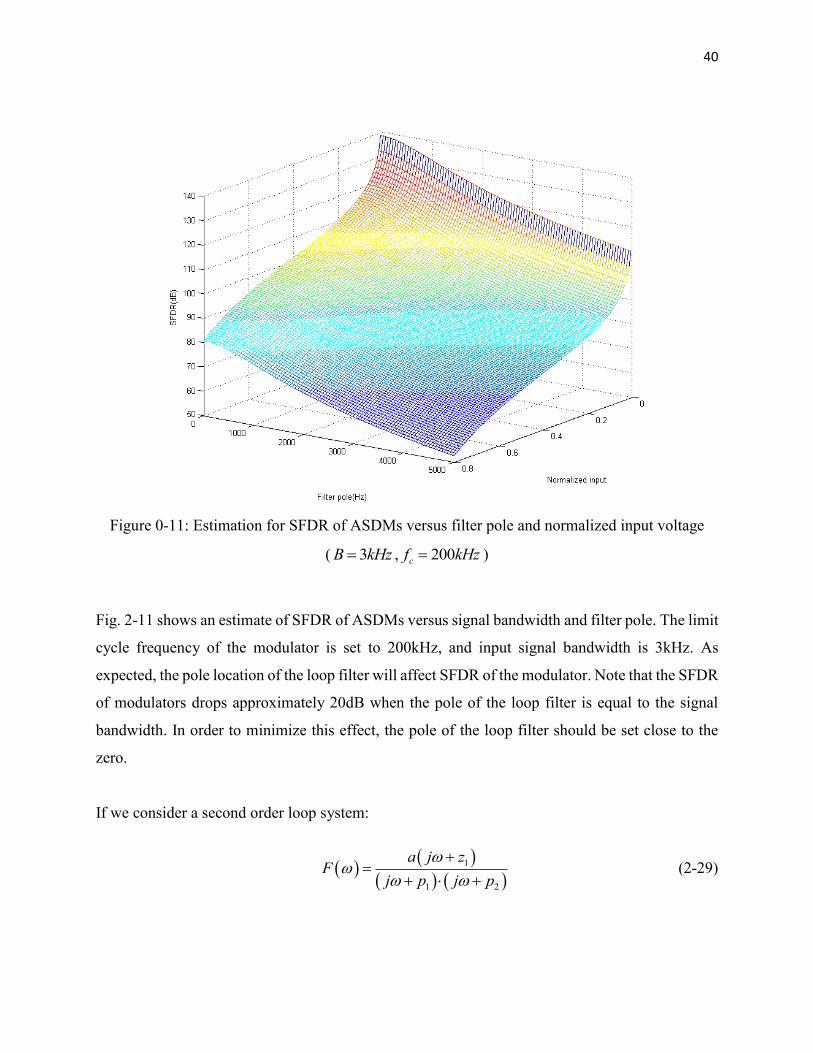
Figure 0-11: Estimation for SFDR of ASDMs versus filter pole and normalized input voltage
( 3B kHz , 200cf kHz )
Fig. 2-11 shows an estimate of SFDR of ASDMs versus signal bandwidth and filter pole. The limit
cycle frequency of the modulator is set to 200kHz, and input signal bandwidth is 3kHz. As
expected, the pole location of the loop filter will affect SFDR of the modulator. Note that the SFDR
of modulators drops approximately 20dB when the pole of the loop filter is equal to the signal
bandwidth. In order to minimize this effect, the pole of the loop filter should be set close to the
zero.
If we consider a second order loop system:
1
1 2
a j zF
j p j p
(2-29)
41
The third harmonic distortion can be rewritten as:
2 2 2 2 22 2 2 21 20 2 2 20
3 2 22 2 2 200 1 0 2
Re
24 Re 24 24
p pFV V V
F p p
(2-30)
Where 2
1 20 2
12 1
p p V
bz V
, 1 2 0,p p
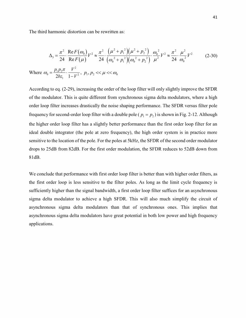
According to eq. (2-29), increasing the order of the loop filter will only slightly improve the SFDR
of the modulator. This is quite different from synchronous sigma delta modulators, where a high
order loop filter increases drastically the noise shaping performance. The SFDR versus filter pole
frequency for second-order loop filter with a double pole ( 1 2p p ) is shown in Fig. 2-12. Although
the higher order loop filter has a slightly better performance than the first order loop filter for an
ideal double integrator (the pole at zero frequency), the high order system is in practice more
sensitive to the location of the pole. For the poles at 5kHz, the SFDR of the second order modulator
drops to 25dB from 82dB. For the first order modulation, the SFDR reduces to 52dB down from
81dB.
We conclude that performance with first order loop filter is better than with higher order filters, as
the first order loop is less sensitive to the filter poles. As long as the limit cycle frequency is
sufficiently higher than the signal bandwidth, a first order loop filter suffices for an asynchronous
sigma delta modulator to achieve a high SFDR. This will also much simplify the circuit of
asynchronous sigma delta modulators than that of synchronous ones. This implies that
asynchronous sigma delta modulators have great potential in both low power and high frequency
applications.
42
Figure 0-12: Comparison of SFDR between the first order and second loop filters versus pole
location ( 3B kHz , 0.8V , 200cf kHz )
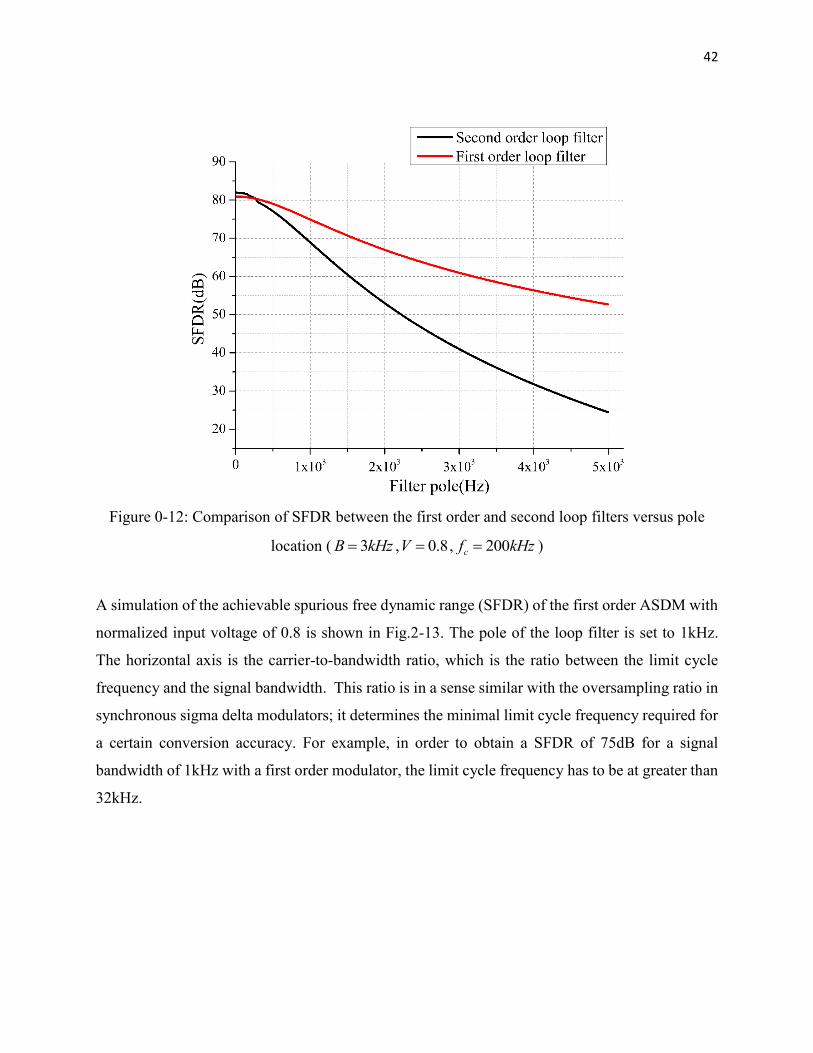
A simulation of the achievable spurious free dynamic range (SFDR) of the first order ASDM with
normalized input voltage of 0.8 is shown in Fig.2-13. The pole of the loop filter is set to 1kHz.
The horizontal axis is the carrier-to-bandwidth ratio, which is the ratio between the limit cycle
frequency and the signal bandwidth. This ratio is in a sense similar with the oversampling ratio in
synchronous sigma delta modulators; it determines the minimal limit cycle frequency required for
a certain conversion accuracy. For example, in order to obtain a SFDR of 75dB for a signal
bandwidth of 1kHz with a first order modulator, the limit cycle frequency has to be at greater than
32kHz.
43
Figure 0-13: Estimation for the achievable SFDR of the first order ASDM ( 0.8V , 3inf B ,
1 1p kHz )
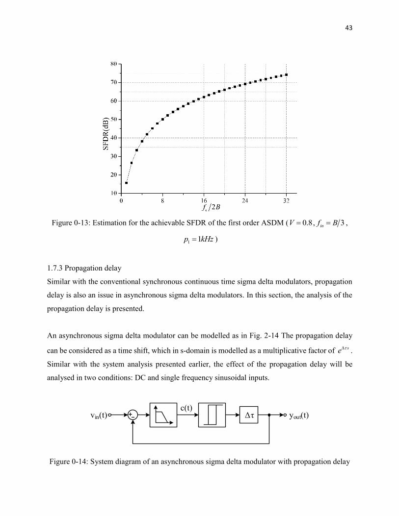
1.7.3 Propagation delay
Similar with the conventional synchronous continuous time sigma delta modulators, propagation
delay is also an issue in asynchronous sigma delta modulators. In this section, the analysis of the
propagation delay is presented.
An asynchronous sigma delta modulator can be modelled as in Fig. 2-14 The propagation delay
can be considered as a time shift, which in s-domain is modelled as a multiplicative factor of se .
Similar with the system analysis presented earlier, the effect of the propagation delay will be
analysed in two conditions: DC and single frequency sinusoidal inputs.
vin(t) yout(t)c(t)
Δτ
Figure 0-14: System diagram of an asynchronous sigma delta modulator with propagation delay
44
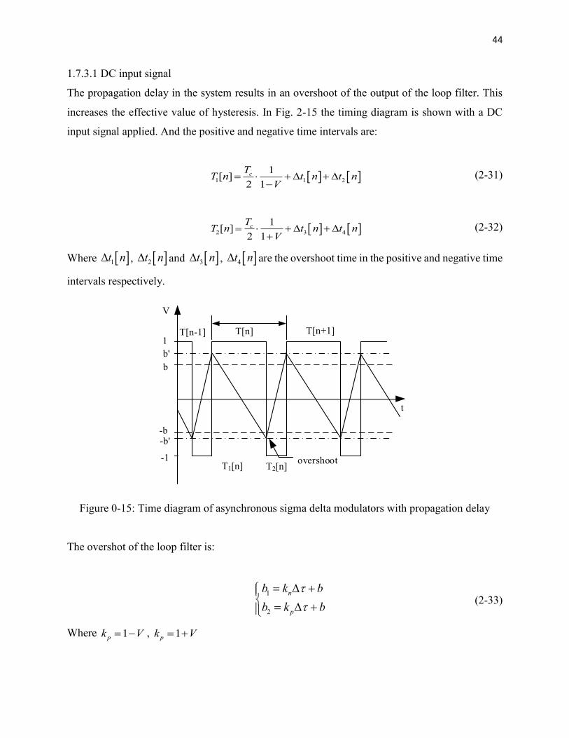
1.7.3.1 DC input signal
The propagation delay in the system results in an overshoot of the output of the loop filter. This
increases the effective value of hysteresis. In Fig. 2-15 the timing diagram is shown with a DC
input signal applied. And the positive and negative time intervals are:
1 1 2
1[ ]
2 1
cTT n t n t n
V
(2-31)
2 3 4
1[ ]
2 1
cTT n t n t n
V
(2-32)
Where 1t n , 2t n and 3t n , 4t n are the overshoot time in the positive and negative time
intervals respectively.
V
t
1
-1
T[n] T[n+1]T[n-1]
overshoot
-b-b'
b
b'
T1[n] T2[n]
Figure 0-15: Time diagram of asynchronous sigma delta modulators with propagation delay
The overshot of the loop filter is:
1
2
n
p
b k b
b k b
(2-33)
Where 1pk V , 1pk V
45
Hence the relationship between delay times in each time interval can be shown to be:
3 2 2
[ ] 1[ ] [ ] [ ]
[ ] 1
p
n
k n Vt n t n t n
k n V
(2-34)
4 1 1
[ ] 1[ ] [ 1] [ ]
[ 1] 1
p
n
k n Vt n t n t n
k n V
(2-35)
Where 1 1 11t n t n t .
In this case the output instantaneous frequency of the modulator becomes:
0 2 1
2 2 2[ ] [ ]
2 1 1 1 1
cTT t n t n
V V V V
(2-36)
When the input is zero, the limit cycle frequency becomes:
1
4cf
b
(2-37)
Whereb is the effective value of the hysteresis.
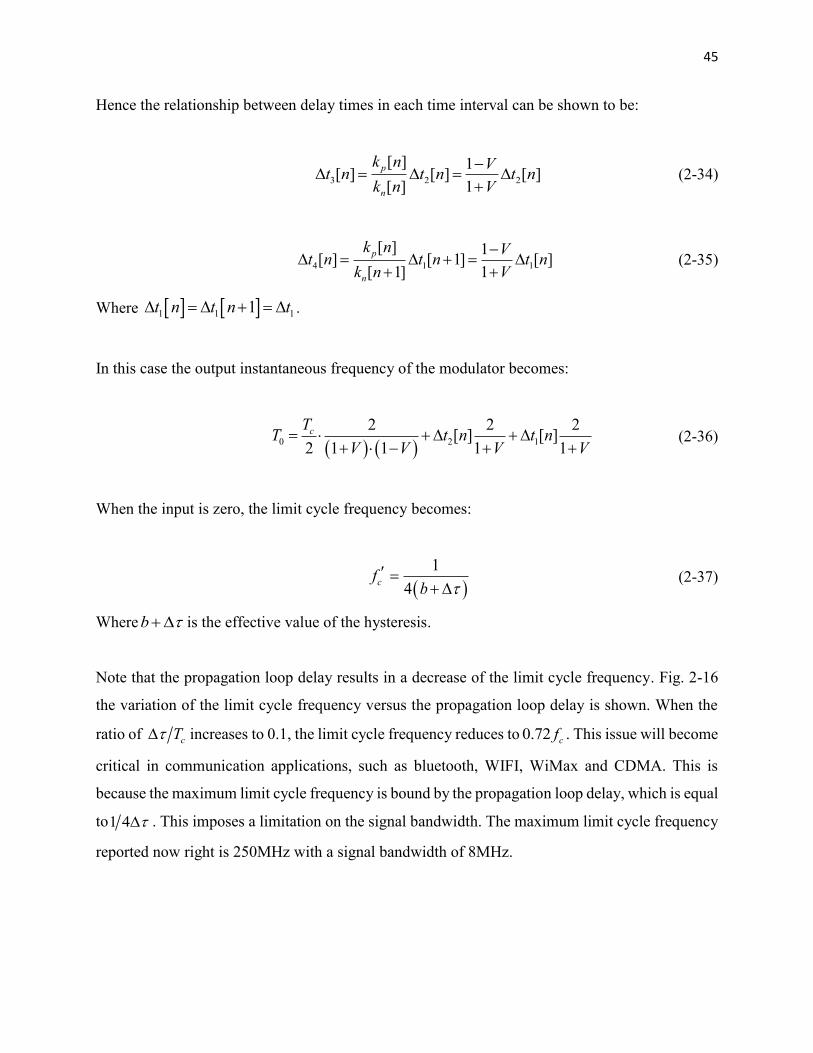
Note that the propagation loop delay results in a decrease of the limit cycle frequency. Fig. 2-16
the variation of the limit cycle frequency versus the propagation loop delay is shown. When the
ratio of cT increases to 0.1, the limit cycle frequency reduces to 0.72 cf . This issue will become
critical in communication applications, such as bluetooth, WIFI, WiMax and CDMA. This is
because the maximum limit cycle frequency is bound by the propagation loop delay, which is equal
to1 4 . This imposes a limitation on the signal bandwidth. The maximum limit cycle frequency
reported now right is 250MHz with a signal bandwidth of 8MHz.
46
Figure 0-16: Variation of the limit cycle frequency versus the propagation loop delay
According to Fig. 2-15, the duty cycle of the output waveform can be easily derived as:
1 21
2 1
1[ ] [ ]
[ ] 12 12 2 2 2
[ ] [ ]2 1 1 1 1
c
cc
Tt n t n
T n VVTT
t n t nV V V V
(2-38)
Here we assume that the propagation delay in the loop is constant. Note that for a DC input signal
V , the propagation delay will not affect the duty cycle of asynchronous sigma delta modulators.
1.7.3.2 The sinusoidal input signal
For a sinusoidal input signal eq. (2-13) can be rewritten as:
inv y t f t c t (2-39)
Using the convolution theorem (Appendix II), the following equations can be obtained:
47
0
1 0
2
0
1 0
2 2 sin 2cos 2 1 Re 1 Re sin 2
4
cos
sinIm sin 2
4 4 2
n
m
n
m
c
c
n
nV T F F n
n T
a V TT
b aTn
F nn T
(2-40)
Where 0
4a
A b
.
Note that the propagation loop delay introduces a bias drift to the modulator, which has the same
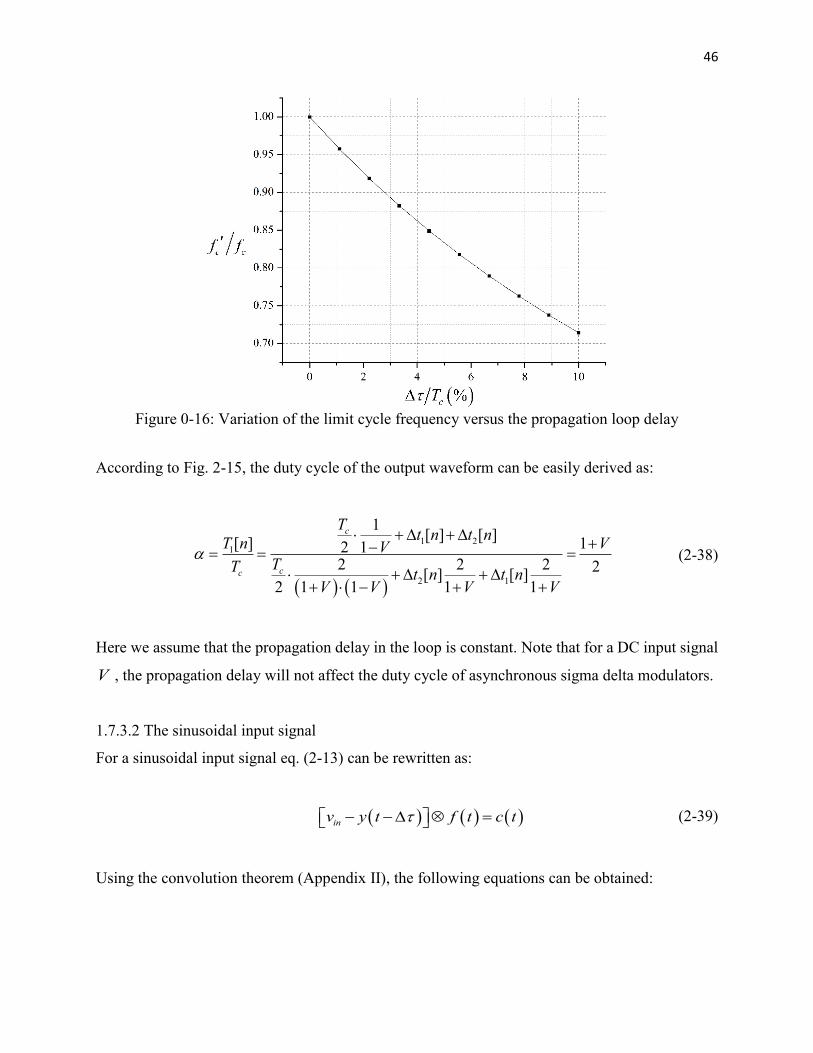
shape and phase of the input signal as shown in Fig. 2-17.
Figure 0-17: Phenomenon of propagation delay
For an ideal integrator, the third order harmonic distortion can be derived as:
2
3 2
0 0
2sin 2
24 4T
(2-41)
48
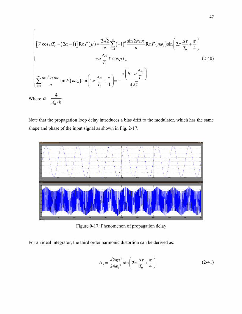
Compared with eq. (2-27), the propagation loop delay results in the distortion function a factor
0
2 sin 24T
. The SFDR versus the propagation loop delay is shown in Fig. 2-18. Note
that 0.1 cT will result in a 8.5dB decrease in SFDR. It can therefore be concluded that the
propagation loop delay limits the limit cycle frequency of asynchronous sigma delta modulators,
which in turn limits the signal bandwidth if the SFDR of the system is maintained to a certain level.
For example, for a 40ps loop delay, the limit cycle frequency will be limited to 250MHz in order
to maintain the value of cT within 1%.
Figure 0-18: SFDR of asynchronous sigma delta modulators with propagation loop delay
1.7.4 The state-of-art of asynchronous sigma delta modulators
Asynchronous sigma delta modulators were first proposed in 1975. Very few publications have
appeared over nearly 35 years (Fig. 2-19). This is because synchronous sigma delta modulators
were very robust with the effect of oversampling and noise shaping. However, the conventional
signal delta modulator is reaching its limits of acceptable power consumption and the maximum
speed supported by CMOS technology. During the last 10 years, asynchronous sigma delta
modulators have been increasing explored as a potential solution of the problems associated with
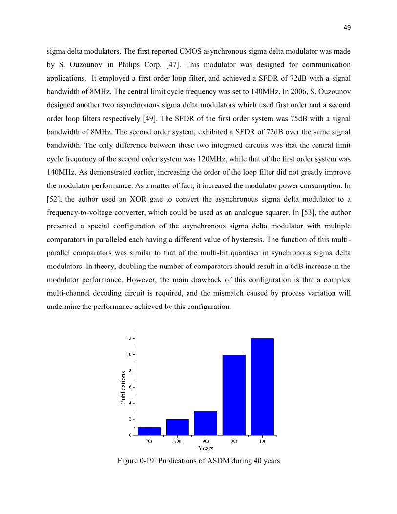
49
sigma delta modulators. The first reported CMOS asynchronous sigma delta modulator was made
by S. Ouzounov in Philips Corp. [47]. This modulator was designed for communication
applications. It employed a first order loop filter, and achieved a SFDR of 72dB with a signal
bandwidth of 8MHz. The central limit cycle frequency was set to 140MHz. In 2006, S. Ouzounov
designed another two asynchronous sigma delta modulators which used first order and a second
order loop filters respectively [49]. The SFDR of the first order system was 75dB with a signal
bandwidth of 8MHz. The second order system, exhibited a SFDR of 72dB over the same signal
bandwidth. The only difference between these two integrated circuits was that the central limit
cycle frequency of the second order system was 120MHz, while that of the first order system was
140MHz. As demonstrated earlier, increasing the order of the loop filter did not greatly improve
the modulator performance. As a matter of fact, it increased the modulator power consumption. In
[52], the author used an XOR gate to convert the asynchronous sigma delta modulator to a
frequency-to-voltage converter, which could be used as an analogue squarer. In [53], the author
presented a special configuration of the asynchronous sigma delta modulator with multiple
comparators in paralleled each having a different value of hysteresis. The function of this multi-
parallel comparators was similar to that of the multi-bit quantiser in synchronous sigma delta
modulators. In theory, doubling the number of comparators should result in a 6dB increase in the
modulator performance. However, the main drawback of this configuration is that a complex
multi-channel decoding circuit is required, and the mismatch caused by process variation will
undermine the performance achieved by this configuration.
Figure 0-19: Publications of ASDM during 40 years
50
A drawback of asynchronous sigma delta modulators, relative to synchronous ones is the absence
of noise shaping. Some author have proposed combining synchronous and asynchronous sigma
delta modulators to solve this problem. In [54], a combination modulator was presented, in which
a sample clock was inserted to the loop of the asynchronous sigma delta modulator. This way, first
order noise shaping was obtained with a first order modulator. This configuration can be extended
to high order systems to obtain a high order noise shaping. However, this way has been sacrificed
one of the main advantages of asynchronous sigma delta modulators. This kind of modulator
belongs to the class of synchronous sigma delta modulators, since a sampling clock is used to
synchronize the binary output. More details of trade-offs involved in noise shaping are presented
in Chapter 4.
Currently, asynchronous sigma delta modulators are also proposed for ultra-low power
applications. In [55], an asynchronous sigma delta modulator was employed as a signal encoding
machine in an electroencephalograph (EEG) system. The limit cycle frequency of this modulator
was 1kHz.
1.8 Summary
This chapter provided a brief introduction to the fundamental theory of conventional synchronous
sigma delta modulators. The classical configuration and important design equations were
discussed. A literature review of recent integrated implementations of synchronous sigma delta
modulators was also presented. The drawbacks of synchronous sigma delta modulators were
introduced. The asynchronous sigma delta modulators were introduced as s solution to the
limitations of synchronous modulators. The fundamental system analysis asynchronous sigma
delta modulators was presented in detail. The noise performance and important non-ideal effects
including harmonic distortion and the effect of loop propagation delay were explained. The
fundamental theory presented in this chapter will be frequency referred to and used throughout the
dissertation.
51
The Asynchronous Sigma Delta Modulator
with a Novel Time-to-Digital Converter
1.9 Introduction
The analysis of asynchronous sigma delta modulators was presented in Chapter 2. Asynchronous
sigma delta modulators have many advantages, including the absence of quantisation errors, and
immunity to clock jitter. When this modulator is used for data conversion, the main challenge is
how to extract the information from the modulated square wave and how to synchronize to the
digital output.
In theory, the signal can be recovered by applying an ideal low pass filter with a cut-off frequency
at the signal bandwidth. When asynchronous sigma delta modulators are used in A/D data
conversion, a decoding circuit is required. The simplest one is the sample & hold (Fig.3-1). The
total noise power NP within a bandwidth B amounts to [45]
2
0
8
3N sP f T B (3-1)
The signal-to-noise ratio (SNR) of such a modulator can be described by:
22
220
3
2 1
sfVSNR F
fV
(3-2)
Where 2cF f B is the carrier-to-bandwidth ratio, V is the normalized input amplitude.
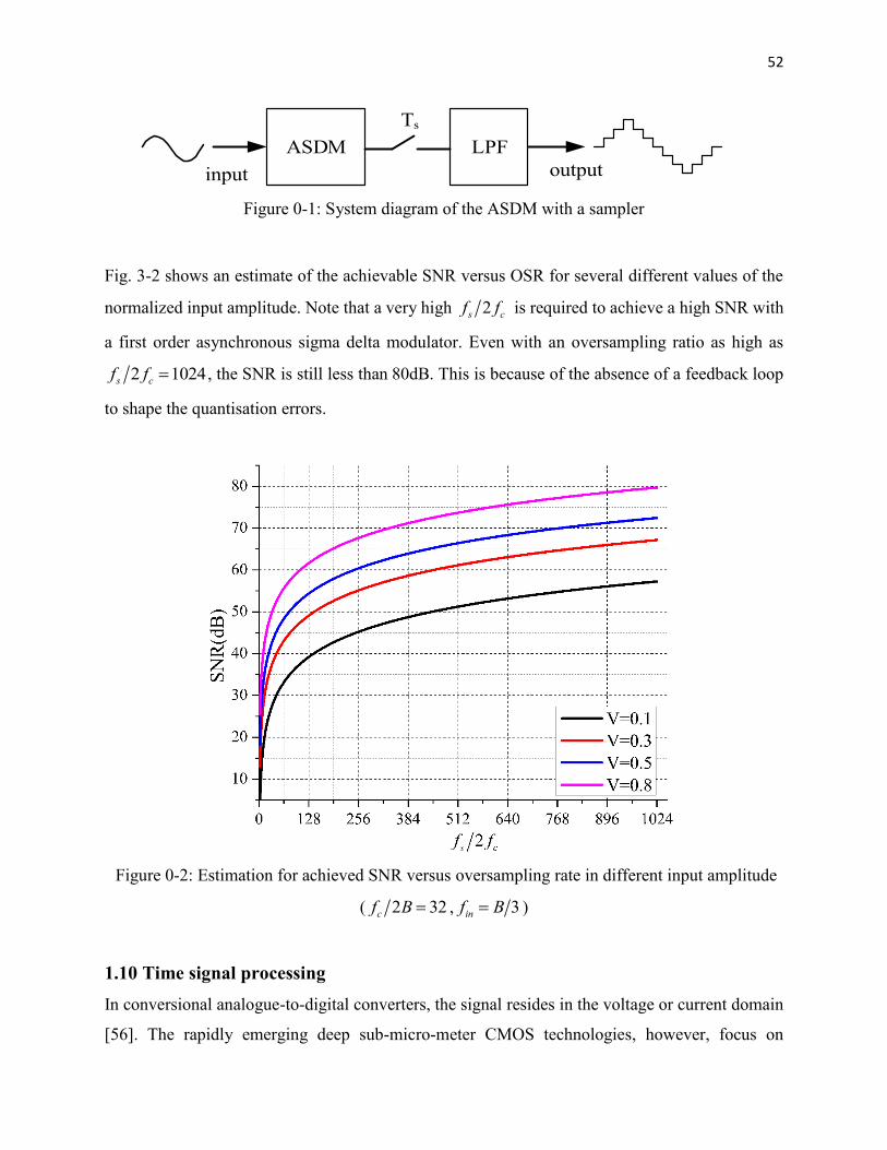
52
ASDM LPF
input output
Ts
Figure 0-1: System diagram of the ASDM with a sampler
Fig. 3-2 shows an estimate of the achievable SNR versus OSR for several different values of the
normalized input amplitude. Note that a very high 2s cf f is required to achieve a high SNR with
a first order asynchronous sigma delta modulator. Even with an oversampling ratio as high as
2 1024s cf f , the SNR is still less than 80dB. This is because of the absence of a feedback loop
to shape the quantisation errors.
Figure 0-2: Estimation for achieved SNR versus oversampling rate in different input amplitude
( 2 32cf B , 3inf B )
1.10 Time signal processing
In conversional analogue-to-digital converters, the signal resides in the voltage or current domain
[56]. The rapidly emerging deep sub-micro-meter CMOS technologies, however, focus on
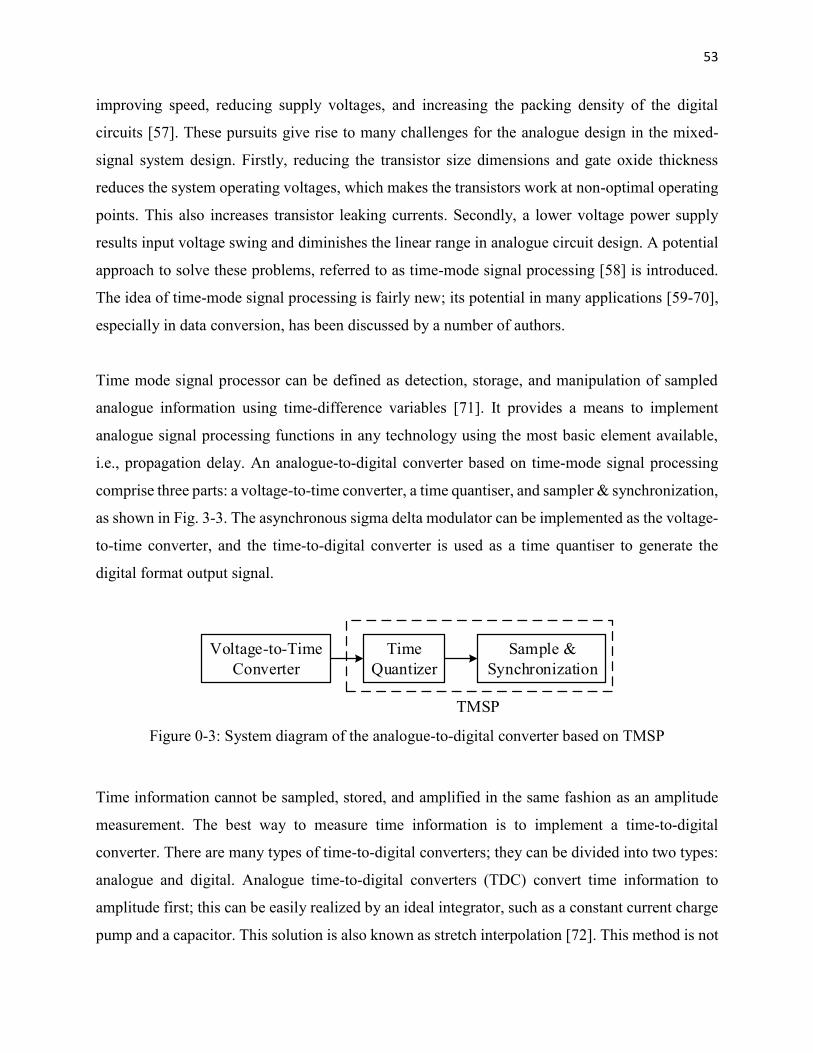
53
improving speed, reducing supply voltages, and increasing the packing density of the digital
circuits [57]. These pursuits give rise to many challenges for the analogue design in the mixed-
signal system design. Firstly, reducing the transistor size dimensions and gate oxide thickness
reduces the system operating voltages, which makes the transistors work at non-optimal operating
points. This also increases transistor leaking currents. Secondly, a lower voltage power supply
results input voltage swing and diminishes the linear range in analogue circuit design. A potential
approach to solve these problems, referred to as time-mode signal processing [58] is introduced.
The idea of time-mode signal processing is fairly new; its potential in many applications [59-70],
especially in data conversion, has been discussed by a number of authors.
Time mode signal processor can be defined as detection, storage, and manipulation of sampled
analogue information using time-difference variables [71]. It provides a means to implement
analogue signal processing functions in any technology using the most basic element available,
i.e., propagation delay. An analogue-to-digital converter based on time-mode signal processing
comprise three parts: a voltage-to-time converter, a time quantiser, and sampler & synchronization,
as shown in Fig. 3-3. The asynchronous sigma delta modulator can be implemented as the voltage-
to-time converter, and the time-to-digital converter is used as a time quantiser to generate the
digital format output signal.
Voltage-to-Time
Converter
Time
Quantizer
Sample &
Synchronization
TMSP
Figure 0-3: System diagram of the analogue-to-digital converter based on TMSP
Time information cannot be sampled, stored, and amplified in the same fashion as an amplitude
measurement. The best way to measure time information is to implement a time-to-digital
converter. There are many types of time-to-digital converters; they can be divided into two types:
analogue and digital. Analogue time-to-digital converters (TDC) convert time information to
amplitude first; this can be easily realized by an ideal integrator, such as a constant current charge
pump and a capacitor. This solution is also known as stretch interpolation [72]. This method is not
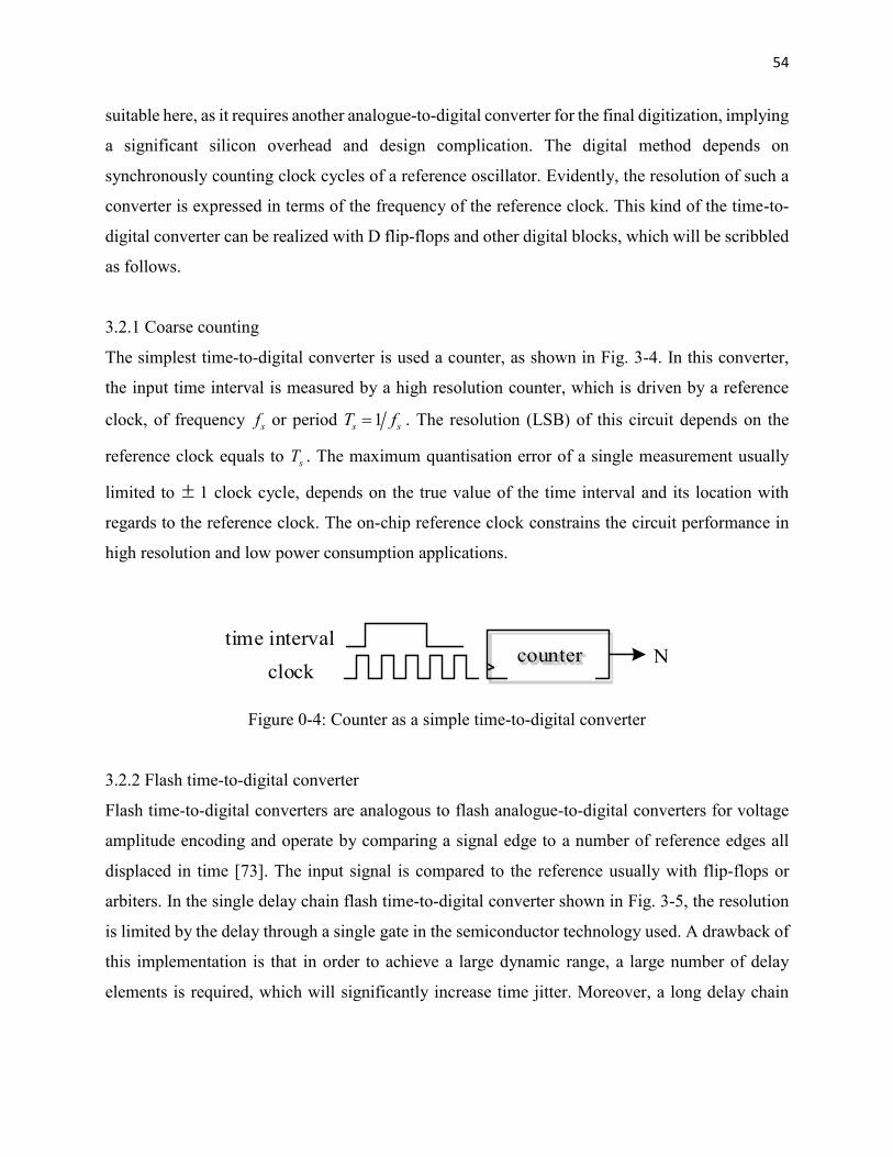
54
suitable here, as it requires another analogue-to-digital converter for the final digitization, implying
a significant silicon overhead and design complication. The digital method depends on
synchronously counting clock cycles of a reference oscillator. Evidently, the resolution of such a
converter is expressed in terms of the frequency of the reference clock. This kind of the time-to-
digital converter can be realized with D flip-flops and other digital blocks, which will be scribbled
as follows.
3.2.1 Coarse counting
The simplest time-to-digital converter is used a counter, as shown in Fig. 3-4. In this converter,
the input time interval is measured by a high resolution counter, which is driven by a reference
clock, of frequency sf or period 1s sT f . The resolution (LSB) of this circuit depends on the
reference clock equals to sT . The maximum quantisation error of a single measurement usually
limited to 1 clock cycle, depends on the true value of the time interval and its location with
regards to the reference clock. The on-chip reference clock constrains the circuit performance in
high resolution and low power consumption applications.
counterclock
time intervalN
Figure 0-4: Counter as a simple time-to-digital converter
3.2.2 Flash time-to-digital converter
Flash time-to-digital converters are analogous to flash analogue-to-digital converters for voltage
amplitude encoding and operate by comparing a signal edge to a number of reference edges all
displaced in time [73]. The input signal is compared to the reference usually with flip-flops or
arbiters. In the single delay chain flash time-to-digital converter shown in Fig. 3-5, the resolution
is limited by the delay through a single gate in the semiconductor technology used. A drawback of
this implementation is that in order to achieve a large dynamic range, a large number of delay
elements is required, which will significantly increase time jitter. Moreover, a long delay chain
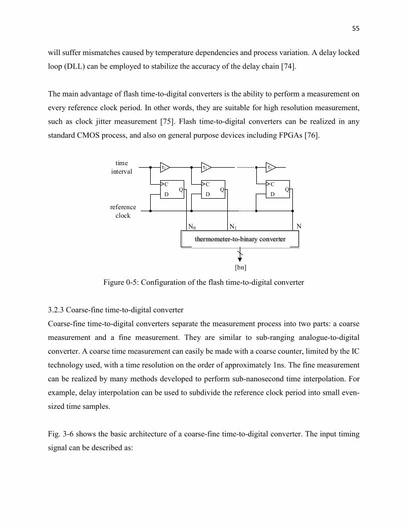
55
will suffer mismatches caused by temperature dependencies and process variation. A delay locked
loop (DLL) can be employed to stabilize the accuracy of the delay chain [74].
The main advantage of flash time-to-digital converters is the ability to perform a measurement on
every reference clock period. In other words, they are suitable for high resolution measurement,
such as clock jitter measurement [75]. Flash time-to-digital converters can be realized in any
standard CMOS process, and also on general purpose devices including FPGAs [76].
C
DQ
τ1
C
DQ
τ1
C
DQ
τ1
time
interval
reference
clock
N0 N1 N
thermometer-to-binary converter
[bn]
Figure 0-5: Configuration of the flash time-to-digital converter
3.2.3 Coarse-fine time-to-digital converter
Coarse-fine time-to-digital converters separate the measurement process into two parts: a coarse
measurement and a fine measurement. They are similar to sub-ranging analogue-to-digital
converter. A coarse time measurement can easily be made with a coarse counter, limited by the IC
technology used, with a time resolution on the order of approximately 1ns. The fine measurement
can be realized by many methods developed to perform sub-nanosecond time interpolation. For
example, delay interpolation can be used to subdivide the reference clock period into small even-
sized time samples.
Fig. 3-6 shows the basic architecture of a coarse-fine time-to-digital converter. The input timing
signal can be described as:
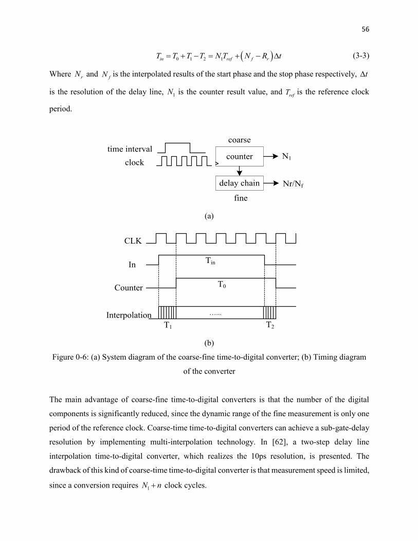
56
0 1 2 1in ref f rT T T T N T N R t (3-3)
Where rN and fN is the interpolated results of the start phase and the stop phase respectively, t
is the resolution of the delay line, 1N is the counter result value, and refT is the reference clock
period.
counter
delay chain
coarse
fine
N1
Nr/Nf
clock
time interval
(a)
CLK
In
Counter T0
Tin
InterpolationT1 T2
…...
(b)
Figure 0-6: (a) System diagram of the coarse-fine time-to-digital converter; (b) Timing diagram
of the converter
The main advantage of coarse-fine time-to-digital converters is that the number of the digital
components is significantly reduced, since the dynamic range of the fine measurement is only one
period of the reference clock. Coarse-time time-to-digital converters can achieve a sub-gate-delay
resolution by implementing multi-interpolation technology. In [62], a two-step delay line
interpolation time-to-digital converter, which realizes the 10ps resolution, is presented. The
drawback of this kind of coarse-time time-to-digital converter is that measurement speed is limited,
since a conversion requires 1N n clock cycles.
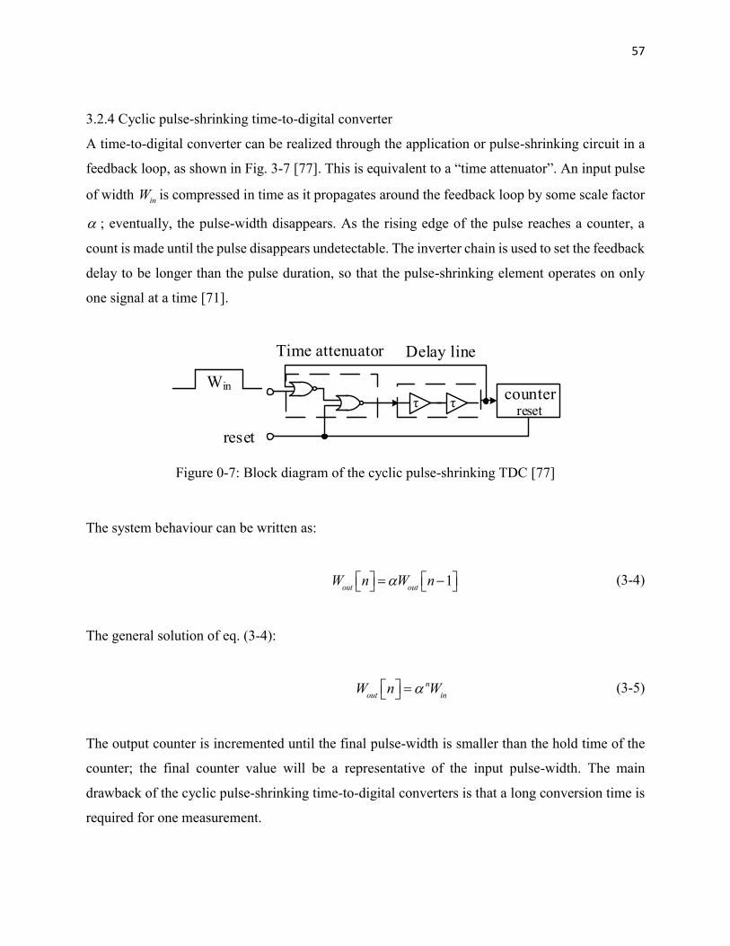
57
3.2.4 Cyclic pulse-shrinking time-to-digital converter
A time-to-digital converter can be realized through the application or pulse-shrinking circuit in a
feedback loop, as shown in Fig. 3-7 [77]. This is equivalent to a “time attenuator”. An input pulse
of width inW is compressed in time as it propagates around the feedback loop by some scale factor
; eventually, the pulse-width disappears. As the rising edge of the pulse reaches a counter, a
count is made until the pulse disappears undetectable. The inverter chain is used to set the feedback
delay to be longer than the pulse duration, so that the pulse-shrinking element operates on only
one signal at a time [71].
counterreset
ττ
Win
reset
Delay lineTime attenuator
Figure 0-7: Block diagram of the cyclic pulse-shrinking TDC [77]
The system behaviour can be written as:
Woutnéë ùû =aWout
n -1éë ùû (3-4)
The general solution of eq. (3-4):
Woutnéë ùû =a
nWin
(3-5)
The output counter is incremented until the final pulse-width is smaller than the hold time of the
counter; the final counter value will be a representative of the input pulse-width. The main
drawback of the cyclic pulse-shrinking time-to-digital converters is that a long conversion time is
required for one measurement.
58
1.11 Time-to-digital converter using vernier delay lines
The relationship of the input signal amplitude and the output square wave can be rewritten as:
1 2
1 2
in
T TV
T T
(3-6)
The conventional method to decode the output signal of the asynchronous sigma delta modulator
is to implement a time-to-digital converter to locate the positive of the time intervals. Assuming
that the output frequency is constant (equivalent to assuming that the input is small), the input
signal can be easily reconstructed:
Vin=N1- N
2
N0
=N1- N
2
N1+ N
2
(3-7)
Where 1 1T N t , 2 2T N t , 0N is constant, and it is equal to the dynamic range of the time-to-
digital converter.
The converter resolution is:
1 2
0 0
1 1 2N NV
N N
(3-8)
However, because of the ASDM’s phase modulation characteristic, the output frequency will
decrease, when the input signal increases. Consequently, the error of the solution above will
significant increase. For instance, when the normalized input voltage is 0.8, the output frequency
will reduce to 0 0.36 cf f , which is almost one third of the limit cycle frequency. One way to solve
this problem is to increase the dynamic range of the time-do-digital converter by a factor of three
relative to the initial one, which will significantly increase the complex of the system. A novel
solution to this issue is presented here, which measures the time intervals 1T and 2T
asynchronously.
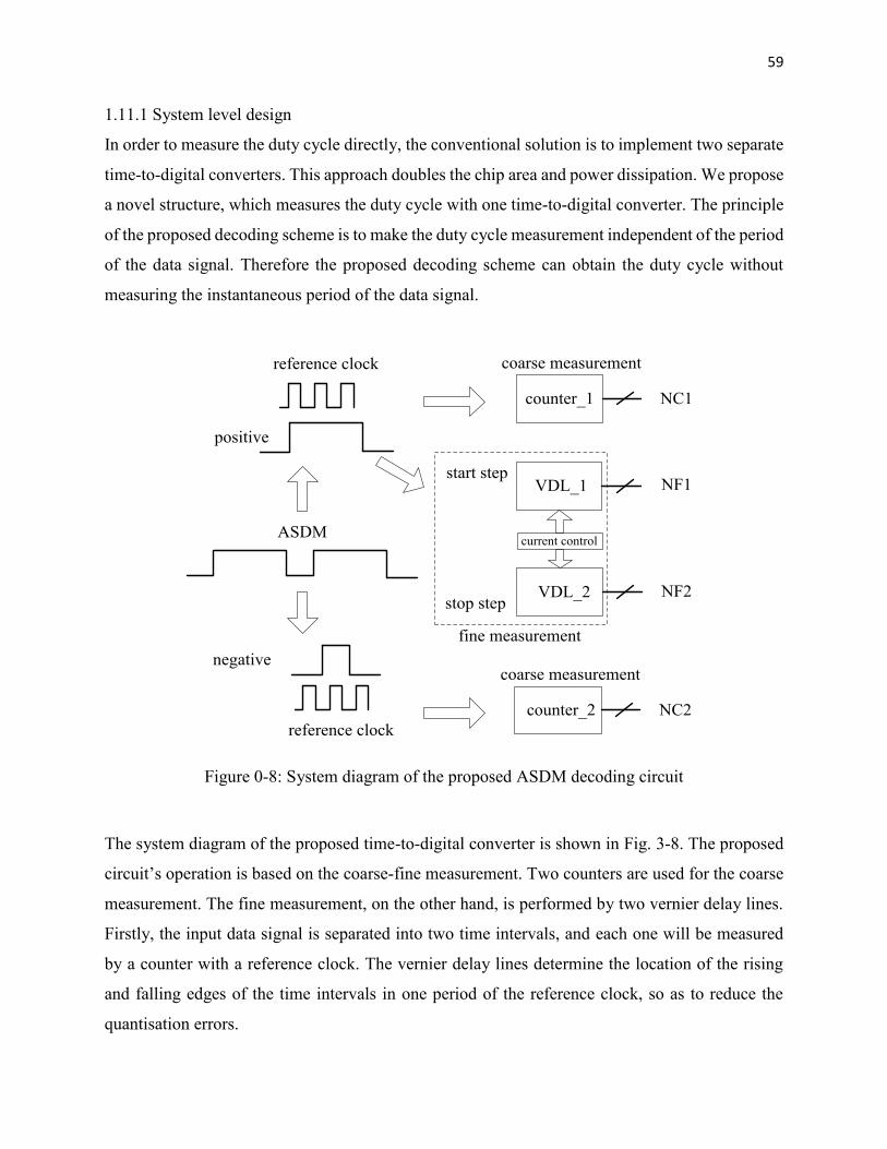
59
1.11.1 System level design
In order to measure the duty cycle directly, the conventional solution is to implement two separate
time-to-digital converters. This approach doubles the chip area and power dissipation. We propose
a novel structure, which measures the duty cycle with one time-to-digital converter. The principle
of the proposed decoding scheme is to make the duty cycle measurement independent of the period
of the data signal. Therefore the proposed decoding scheme can obtain the duty cycle without
measuring the instantaneous period of the data signal.
counter_1 NC1
reference clock
VDL_1
VDL_2
NF1
NF2
ASDMcurrent control
start step
stop step
fine measurement
coarse measurement
counter_2 NC2
coarse measurement
reference clock
positive
negative
Figure 0-8: System diagram of the proposed ASDM decoding circuit
The system diagram of the proposed time-to-digital converter is shown in Fig. 3-8. The proposed
circuit’s operation is based on the coarse-fine measurement. Two counters are used for the coarse
measurement. The fine measurement, on the other hand, is performed by two vernier delay lines.
Firstly, the input data signal is separated into two time intervals, and each one will be measured
by a counter with a reference clock. The vernier delay lines determine the location of the rising
and falling edges of the time intervals in one period of the reference clock, so as to reduce the
quantisation errors.
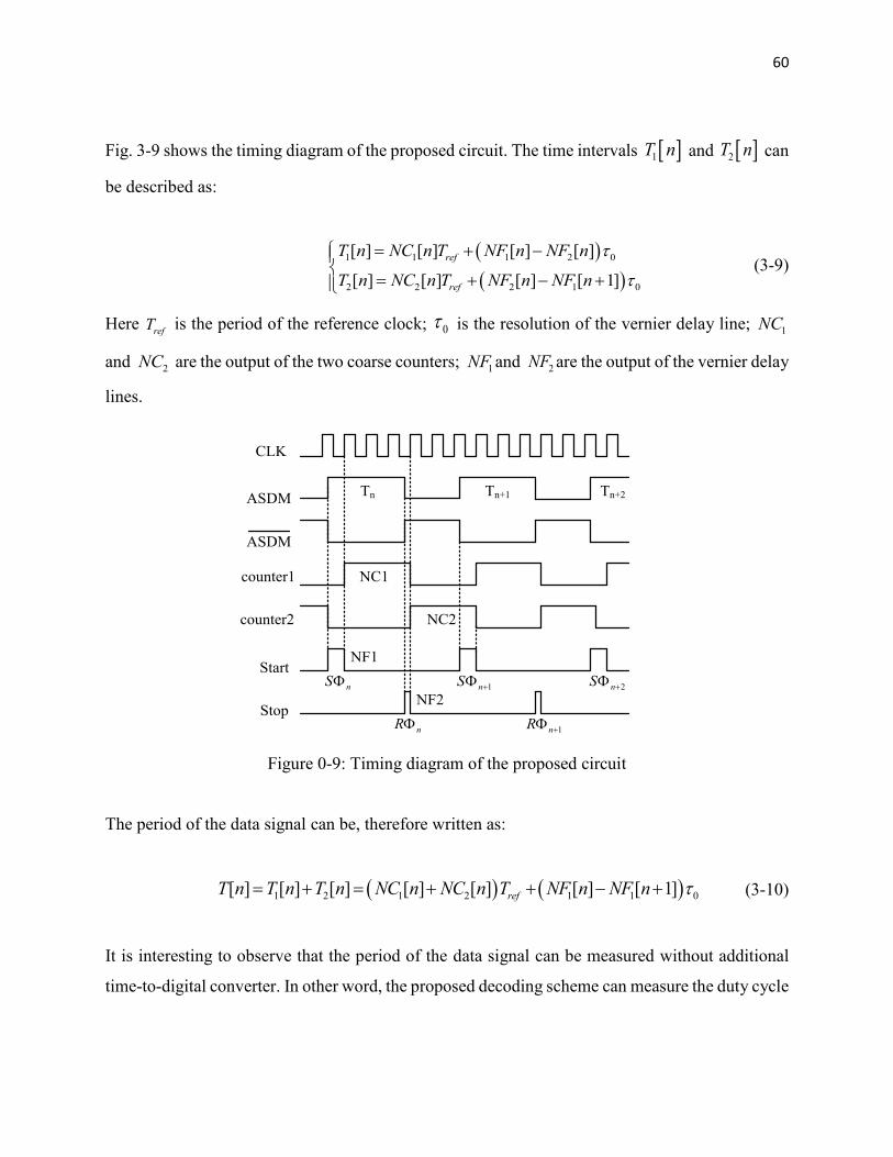
60
Fig. 3-9 shows the timing diagram of the proposed circuit. The time intervals 1T n and 2T n can
be described as:
1 1 1 2 0
2 2 2 1 0
[ ] [ ] [ ] [ ]
[ ] [ ] [ ] [ 1]
ref
ref
T n NC n T NF n NF n
T n NC n T NF n NF n
(3-9)
Here refT is the period of the reference clock; 0 is the resolution of the vernier delay line; 1NC
and 2NC are the output of the two coarse counters; 1NF and 2NF are the output of the vernier delay
lines.
CLK
Start
Stop
ASDM
counter1
NF2
NC1
NF1
ASDM
counter2 NC2
Tn Tn+1 Tn+2
nS 1nS 2nS
nR 1nR
Figure 0-9: Timing diagram of the proposed circuit
The period of the data signal can be, therefore written as:
1 2 1 2 1 1 0[ ] [ ] [ ] [ ] [ ] [ ] [ 1]refT n T n T n NC n NC n T NF n NF n (3-10)
It is interesting to observe that the period of the data signal can be measured without additional
time-to-digital converter. In other word, the proposed decoding scheme can measure the duty cycle
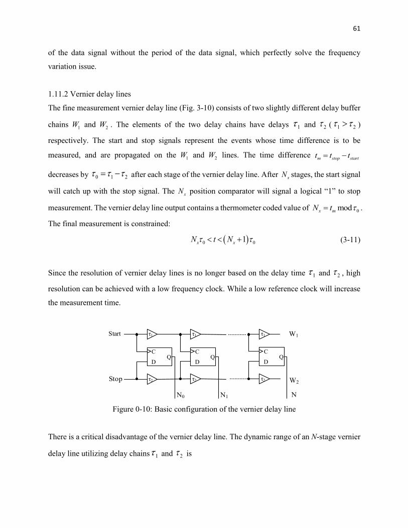
61
of the data signal without the period of the data signal, which perfectly solve the frequency
variation issue.
1.11.2 Vernier delay lines
The fine measurement vernier delay line (Fig. 3-10) consists of two slightly different delay buffer
chains 1W and 2W . The elements of the two delay chains have delays 1 and 2 ( 1 2 )
respectively. The start and stop signals represent the events whose time difference is to be
measured, and are propagated on the 1W and 2W lines. The time difference m stop startt t t
decreases by 0 1 2 after each stage of the vernier delay line. After xN stages, the start signal
will catch up with the stop signal. The xN position comparator will signal a logical “1” to stop
measurement. The vernier delay line output contains a thermometer coded value of 0modx mN t .
The final measurement is constrained:
0 01x xN t N
(3-11)
Since the resolution of vernier delay lines is no longer based on the delay time 1 and 2 , high
resolution can be achieved with a low frequency clock. While a low reference clock will increase
the measurement time.
C
DQ
τ1
τ2
C
DQ
τ1
τ2
C
DQ
τ1
τ2
Start
Stop
N0 N1 N
W1
W2
Figure 0-10: Basic configuration of the vernier delay line
There is a critical disadvantage of the vernier delay line. The dynamic range of an N-stage vernier
delay line utilizing delay chains 1 and 2 is
62
DR RT N (3-12)
While the maximum propagation delay of the vernier delay line is
1MaxT N (3-13)
Note that the MaxT is slightly larger than DRT . This, of course, means that the reset time of the vernier
delay line is larger than its measurement time. Two measurements will overlap, since a
measurement event can start to propagate in the delay line while the previous one is still
propagating. P. Dudek used an extra read-out pipe to solve this problem [78], where the results
stored in the D flip-flops are read out before the next measurement coming.
While this is not an issue with the proposed asynchronous converter. Fig. 3-11 shows one slice of
the proposed vernier delay lines. Two D flip-flops in series are used here and they are triggered by
the rising edge of the input time interval. The first D flip-flop, which is similar as that in basic
vernier delay lines, serves to measure the location of the time interval in one period of the reference
clock. The other one read out the result in the previous one, and feeds it into the thermometer-to-
binary decoder. The maximum transfer speed is the limit cycle frequency of the asynchronous
sigma delta modulator. In order to avoid overlapping, each vernier delay line measurement should
finish before the arrival of the next trigger event. The worst case occurs when the output frequency
is equal to the limit cycle frequency cf , and meanwhile the fine measurement also reaches the
dynamic range. In this case, the time interval is 1 2in cT f , and the measured time for each delay
line is:
1
1 0 1 22
ncm ref
TT N N T (3-14)
Here refT is the reference clock in the counter, 0n is the number of bits of the counter and N is
the output of the vernier delay line.
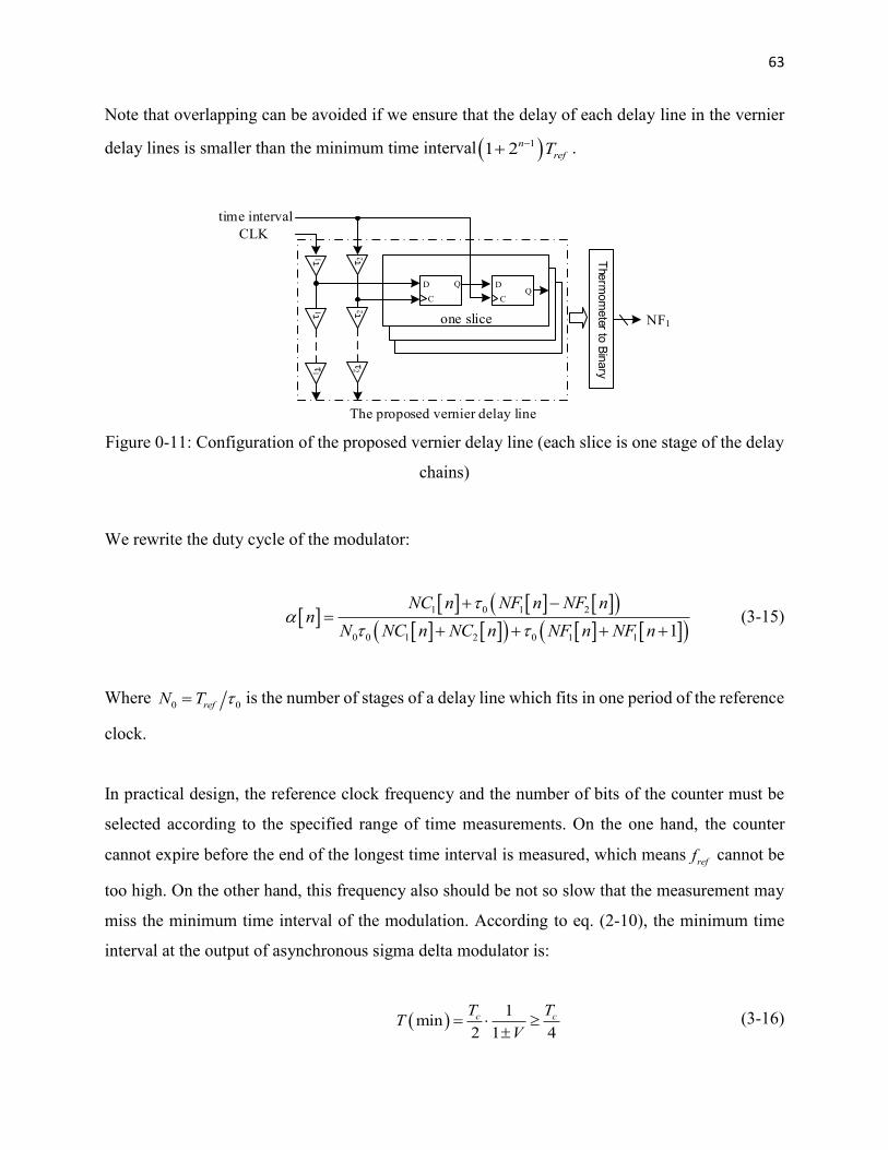
63
Note that overlapping can be avoided if we ensure that the delay of each delay line in the vernier
delay lines is smaller than the minimum time interval 11 2n
refT .
time interval
CLK
C
D Q
C
DQ
τ 1τ 1
τ1
τ 2τ 2
τ2
one slice
The
rmom
eter to
Bin
ary
NF1
The proposed vernier delay line
Figure 0-11: Configuration of the proposed vernier delay line (each slice is one stage of the delay
chains)
We rewrite the duty cycle of the modulator:
1 0 1 2
0 0 1 2 0 1 1 1
NC n NF n NF nn
N NC n NC n NF n NF n
(3-15)
Where 0 0refN T is the number of stages of a delay line which fits in one period of the reference
clock.
In practical design, the reference clock frequency and the number of bits of the counter must be
selected according to the specified range of time measurements. On the one hand, the counter
cannot expire before the end of the longest time interval is measured, which meansreff cannot be
too high. On the other hand, this frequency also should be not so slow that the measurement may
miss the minimum time interval of the modulation. According to eq. (2-10), the minimum time
interval at the output of asynchronous sigma delta modulator is:
1
min2 1 4
c cT TT
V
(3-16)
64
Consequently, the frequency of the reference clock and the number of bits of the counter should
meet the following conditions:
max
2 0 14 1
4
n cref
cref
TT V
V
TT
(3-17)
In practice the modulator will overload when the normalized input amplitude V exceeds the value
of 0.8. The dynamic range of the measurement then is:
2
2max min 2
1 4
ncDR ref
TVT T T T
V
(3-18)
Note that the minimum number of bits of the counter is 4, when the frequency of the reference is
set to be 4ref cf f .
1.11.3 Noise performance
As there is no time quantisation in the asynchronous sigma delta modulator, the signal-to-noise
ratio of the modulator mainly depends on the time-to-digital converter resolution. The minimum
input amplitude, according to eq. (3-15), is:
0 0
2 3
0
2 2 1
2 2n n
c ref
VT T N
(3-19)
Here we assume the variation of the output frequency is very small. The signal-to-noise ratio is
given by the well know quantisation noise expression:
10 06.02 2 1.76 20logSNR n VN (3-20)
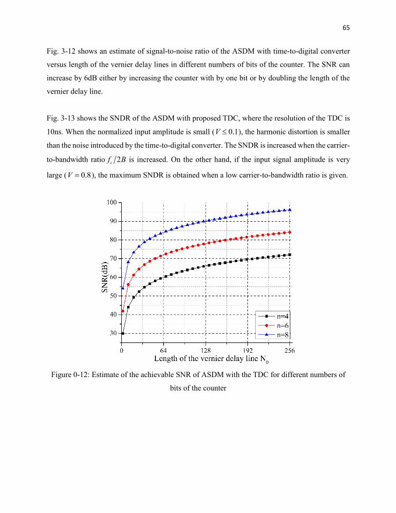
65
Fig. 3-12 shows an estimate of signal-to-noise ratio of the ASDM with time-to-digital converter
versus length of the vernier delay lines in different numbers of bits of the counter. The SNR can
increase by 6dB either by increasing the counter with by one bit or by doubling the length of the
vernier delay line.
Fig. 3-13 shows the SNDR of the ASDM with proposed TDC, where the resolution of the TDC is
10ns. When the normalized input amplitude is small ( 0.1V ), the harmonic distortion is smaller
than the noise introduced by the time-to-digital converter. The SNDR is increased when the carrier-
to-bandwidth ratio 2cf B is increased. On the other hand, if the input signal amplitude is very
large ( 0.8V ), the maximum SNDR is obtained when a low carrier-to-bandwidth ratio is given.
Figure 0-12: Estimate of the achievable SNR of ASDM with the TDC for different numbers of
bits of the counter
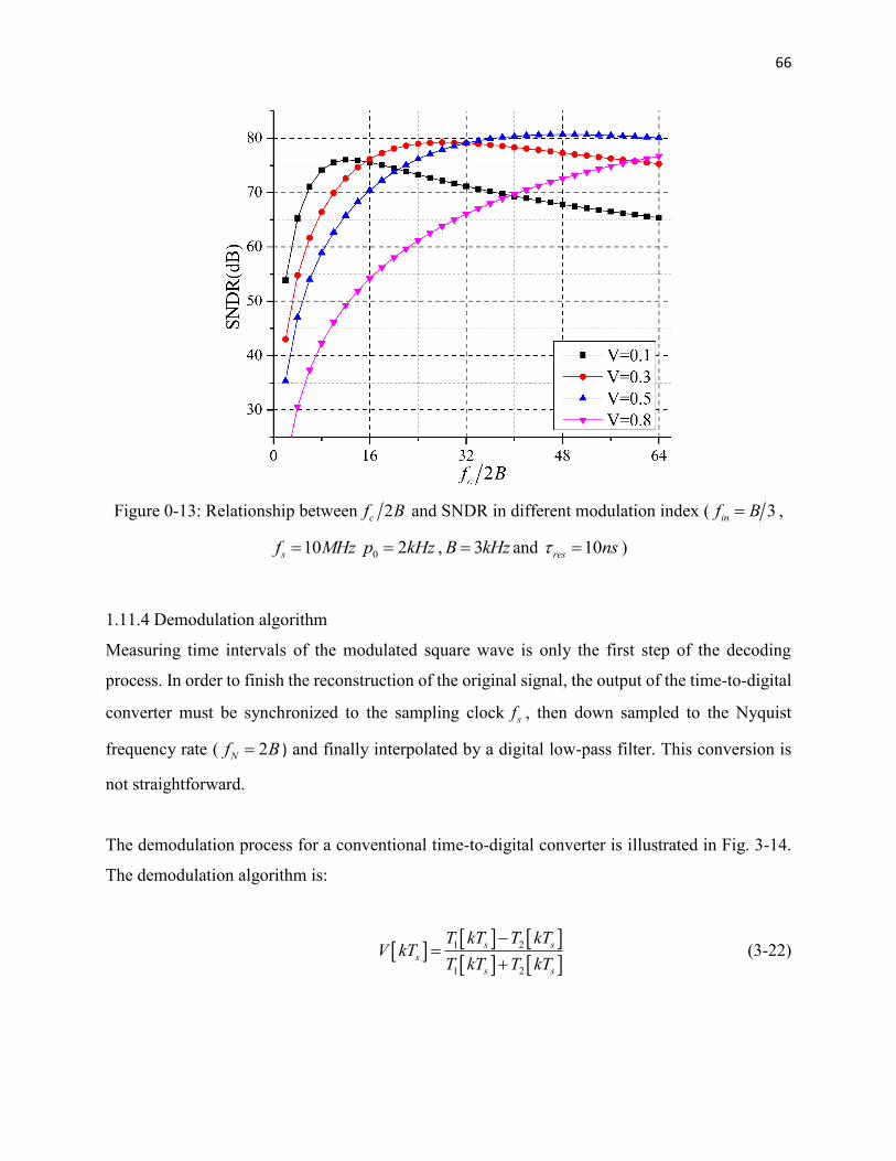
66
Figure 0-13: Relationship between 2cf B and SNDR in different modulation index ( 3inf B ,
10sf MHz 0 2p kHz , 3B kHz and 10res ns )
1.11.4 Demodulation algorithm
Measuring time intervals of the modulated square wave is only the first step of the decoding
process. In order to finish the reconstruction of the original signal, the output of the time-to-digital
converter must be synchronized to the sampling clock sf , then down sampled to the Nyquist
frequency rate ( 2Nf B ) and finally interpolated by a digital low-pass filter. This conversion is
not straightforward.
The demodulation process for a conventional time-to-digital converter is illustrated in Fig. 3-14.
The demodulation algorithm is:
1 2
1 2
s s
s
s s
T kT T kTV kT
T kT T kT
(3-22)
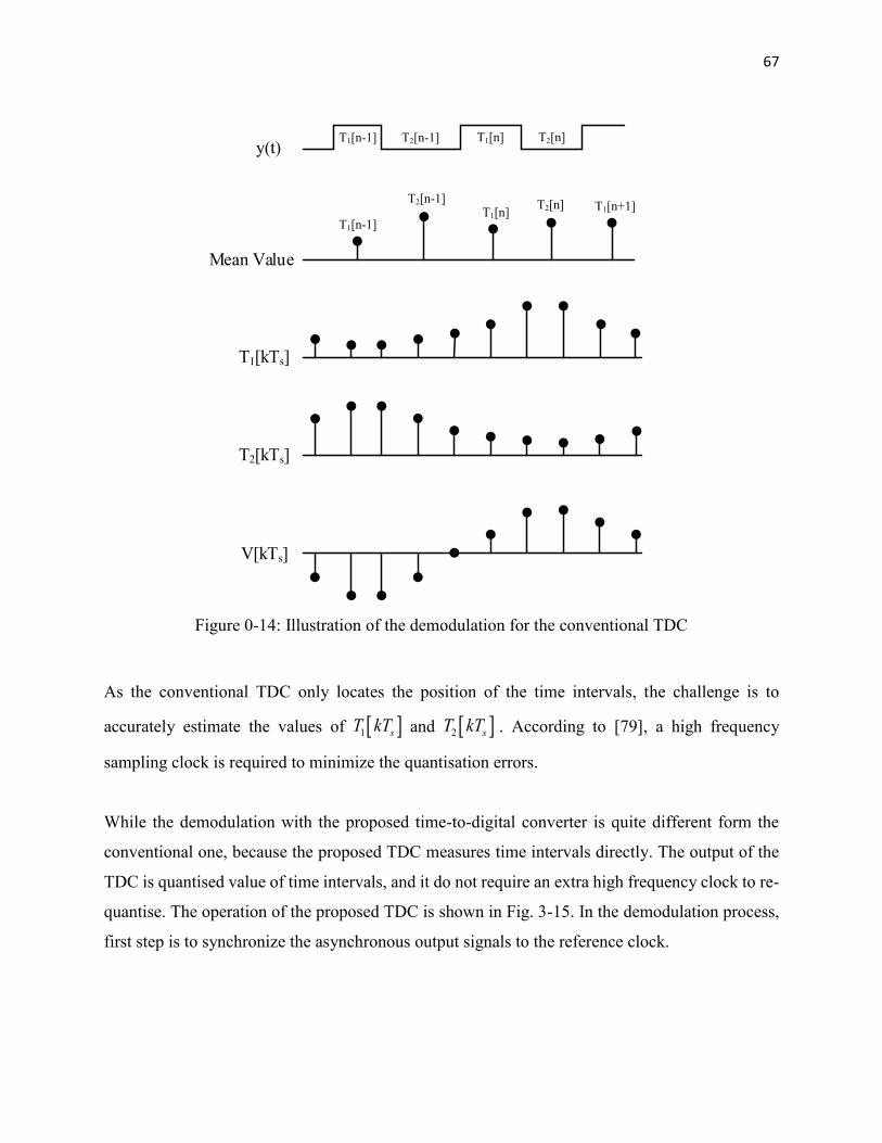
67
T1[n-1] T2[n-1] T1[n] T2[n]
T1[n-1]
T2[n-1]T1[n]
T2[n] T1[n+1]
y(t)
Mean Value
T1[kTs]
T2[kTs]
V[kTs]
Figure 0-14: Illustration of the demodulation for the conventional TDC
As the conventional TDC only locates the position of the time intervals, the challenge is to
accurately estimate the values of 1 sT kT and 2 sT kT . According to [79], a high frequency
sampling clock is required to minimize the quantisation errors.
While the demodulation with the proposed time-to-digital converter is quite different form the
conventional one, because the proposed TDC measures time intervals directly. The output of the
TDC is quantised value of time intervals, and it do not require an extra high frequency clock to re-
quantise. The operation of the proposed TDC is shown in Fig. 3-15. In the demodulation process,
first step is to synchronize the asynchronous output signals to the reference clock.
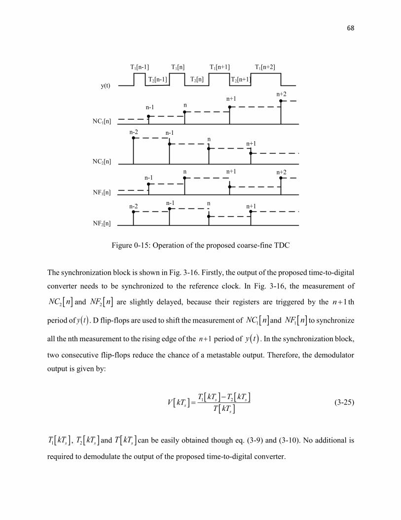
68
T1[n-1]
T2[n-1]
T1[n]
T2[n]y(t)
NC1[n]
NF2[n]
n-1 nn+1
n+2
n-2 n-1n
n+1
n-1
n-1n-2
n
n
n+1
n+1
n+2
NC2[n]
NF1[n]
T1[n+1]
T2[n+1]
T1[n+2]
Figure 0-15: Operation of the proposed coarse-fine TDC
The synchronization block is shown in Fig. 3-16. Firstly, the output of the proposed time-to-digital
converter needs to be synchronized to the reference clock. In Fig. 3-16, the measurement of
2NC n and 2NF n are slightly delayed, because their registers are triggered by the 1n th
period of y t . D flip-flops are used to shift the measurement of 1NC n and 1NF n to synchronize
all the nth measurement to the rising edge of the 1n period of y t . In the synchronization block,
two consecutive flip-flops reduce the chance of a metastable output. Therefore, the demodulator
output is given by:
1 2s s
s
s
T kT T kTV kT
T kT
(3-25)
1 sT kT , 2 sT kT and sT kT can be easily obtained though eq. (3-9) and (3-10). No additional is
required to demodulate the output of the proposed time-to-digital converter.
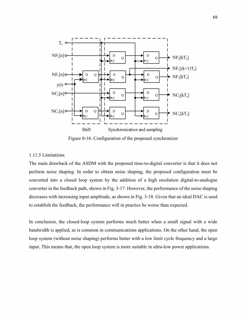
69
C
D
C
Ts
Q DQ
C
D
C
Q DQ
C
DQ
C
DQ
NF2[n]
y(t)C
DQ
C
DQ
C
DQ
C
DQ
NF1[n]
NC1[n]
NC2[n]
NF2[kTs]
NF1[(k+1)Ts]
NF1[kTs]
NC2[kTs]
NC1[kTs]
Shift Synchronization and sampling
Figure 0-16: Configuration of the proposed synchronizer
1.11.5 Limitations
The main drawback of the ASDM with the proposed time-to-digital converter is that it does not
perform noise shaping. In order to obtain noise shaping, the proposed configuration must be
converted into a closed loop system by the addition of a high resolution digital-to-analogue
converter in the feedback path, shown in Fig. 3-17. However, the performance of the noise shaping
decreases with increasing input amplitude, as shown in Fig. 3-18. Given that an ideal DAC is used
to establish the feedback, the performance will in practice be worse than expected.
In conclusion, the closed-loop system performs much better when a small signal with a wide
bandwidth is applied, as is common in communications applications. On the other hand, the open
loop system (without noise shaping) performs better with a low limit cycle frequency and a large
input. This means that, the open loop system is more suitable in ultra-low power applications.
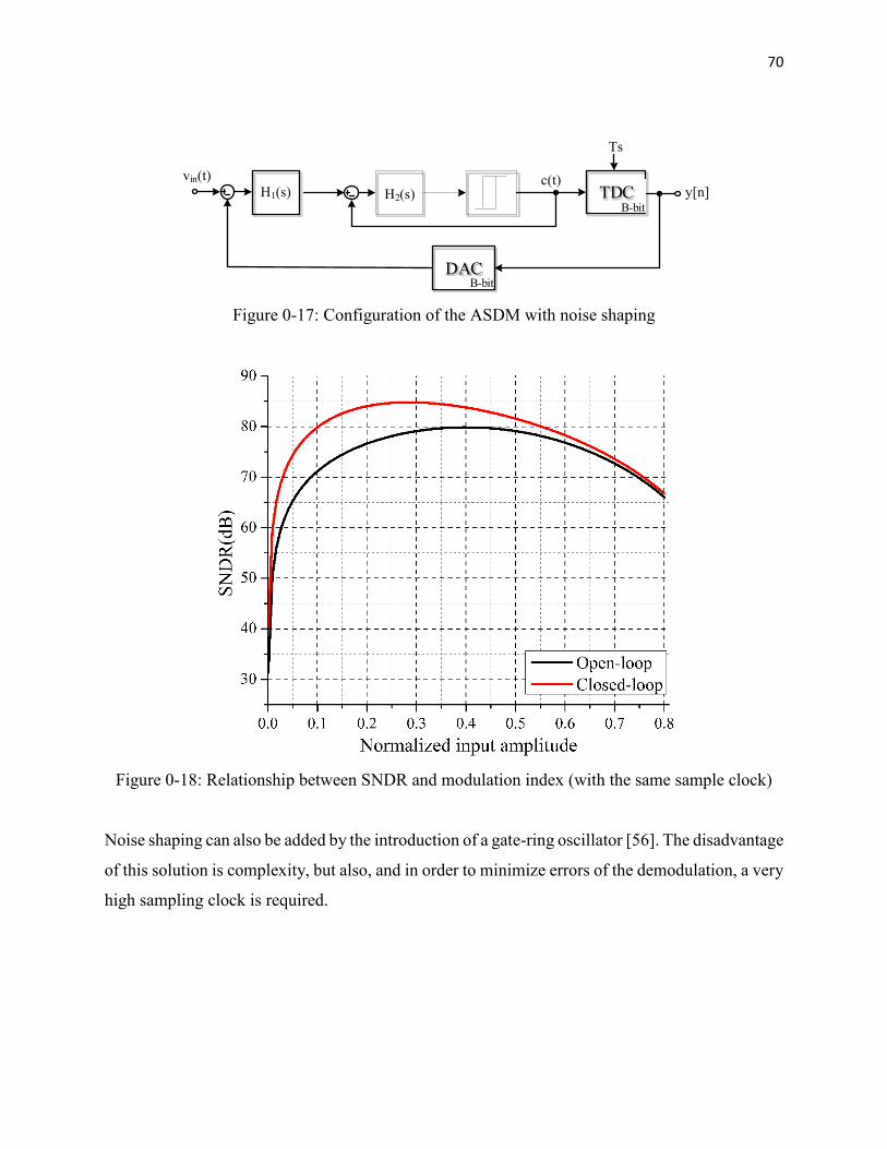
70
c(t)vin(t)
TDCB-bit
Ts
y[n]
DACB-bit
H2(s)H1(s)
Figure 0-17: Configuration of the ASDM with noise shaping
Figure 0-18: Relationship between SNDR and modulation index (with the same sample clock)
Noise shaping can also be added by the introduction of a gate-ring oscillator [56]. The disadvantage
of this solution is complexity, but also, and in order to minimize errors of the demodulation, a very
high sampling clock is required.
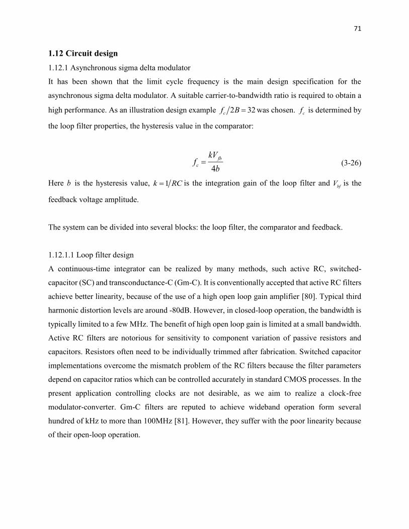
71
1.12 Circuit design
1.12.1 Asynchronous sigma delta modulator
It has been shown that the limit cycle frequency is the main design specification for the
asynchronous sigma delta modulator. A suitable carrier-to-bandwidth ratio is required to obtain a
high performance. As an illustration design example 2 32cf B was chosen. cf is determined by
the loop filter properties, the hysteresis value in the comparator:
4
fb
c
kVf
b (3-26)
Here b is the hysteresis value, 1k RC is the integration gain of the loop filter and bfV is the
feedback voltage amplitude.
The system can be divided into several blocks: the loop filter, the comparator and feedback.
1.12.1.1 Loop filter design
A continuous-time integrator can be realized by many methods, such active RC, switched-
capacitor (SC) and transconductance-C (Gm-C). It is conventionally accepted that active RC filters
achieve better linearity, because of the use of a high open loop gain amplifier [80]. Typical third
harmonic distortion levels are around -80dB. However, in closed-loop operation, the bandwidth is
typically limited to a few MHz. The benefit of high open loop gain is limited at a small bandwidth.
Active RC filters are notorious for sensitivity to component variation of passive resistors and
capacitors. Resistors often need to be individually trimmed after fabrication. Switched capacitor
implementations overcome the mismatch problem of the RC filters because the filter parameters
depend on capacitor ratios which can be controlled accurately in standard CMOS processes. In the
present application controlling clocks are not desirable, as we aim to realize a clock-free
modulator-converter. Gm-C filters are reputed to achieve wideband operation form several
hundred of kHz to more than 100MHz [81]. However, they suffer with the poor linearity because
of their open-loop operation.
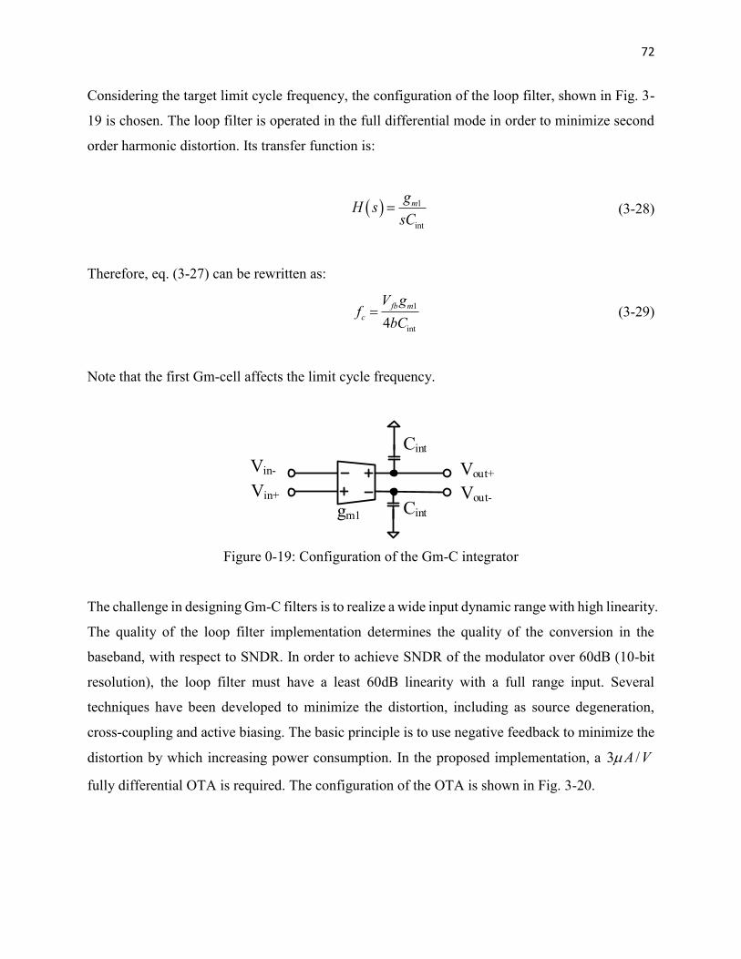
72
Considering the target limit cycle frequency, the configuration of the loop filter, shown in Fig. 3-
19 is chosen. The loop filter is operated in the full differential mode in order to minimize second
order harmonic distortion. Its transfer function is:
1
int
mgH s
sC (3-28)
Therefore, eq. (3-27) can be rewritten as:
1
int4
fb m
c
V gf
bC (3-29)
Note that the first Gm-cell affects the limit cycle frequency.
gm1 Cint
Vout+
Vin+
Cint
Vout-
Vin-
Figure 0-19: Configuration of the Gm-C integrator
The challenge in designing Gm-C filters is to realize a wide input dynamic range with high linearity.
The quality of the loop filter implementation determines the quality of the conversion in the
baseband, with respect to SNDR. In order to achieve SNDR of the modulator over 60dB (10-bit
resolution), the loop filter must have a least 60dB linearity with a full range input. Several
techniques have been developed to minimize the distortion, including as source degeneration,
cross-coupling and active biasing. The basic principle is to use negative feedback to minimize the
distortion by which increasing power consumption. In the proposed implementation, a 3 /A V
fully differential OTA is required. The configuration of the OTA is shown in Fig. 3-20.
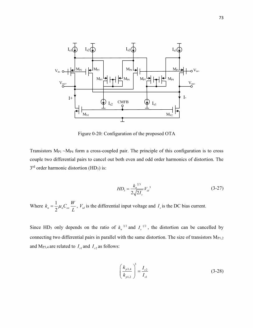
73
Is1Is2
MP1
I-I+
MP2 MP3 MP4 Vin+Vin-
CMFB
MN1 MN2
Is1 Is2
Is2 Is1
MP5 MP6 MP7 MP8
Vout-Vout+
Figure 0-20: Configuration of the proposed OTA
Transistors MP1 ~MP4 form a cross-coupled pair. The principle of this configuration is to cross
couple two differential pairs to cancel out both even and odd order harmonics of distortion. The
3rd order harmonic distortion (HD3) is:
2 33
32 2
nid
s
kHD V
I (3-27)
Where 1
2n n ox
Wk C
L , idV is the differential input voltage and sI is the DC bias current.
Since HD3 only depends on the ratio of 3 2
nk and 1 2
sI , the distortion can be cancelled by
connecting two differential pairs in parallel with the same distortion. The size of transistors MP1,2
and MP3,4 are related to 1sI and 2sI as follows:
3
3,4 2
1,2 1
p s
p s
k I
k I
(3-28)
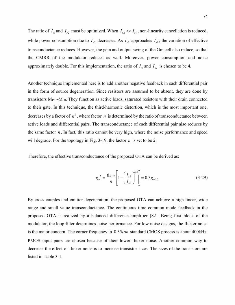
74
The ratio of 1sI and 2sI must be optimized. When 2 1s sI I , non-linearity cancellation is reduced,
while power consumption due to 2sI decreases. As 2sI approaches 1sI , the variation of effective
transconductance reduces. However, the gain and output swing of the Gm cell also reduce, so that
the CMRR of the modulator reduces as well. Moreover, power consumption and noise
approximately double. For this implementation, the ratio of 1sI and 2sI is chosen to be 4.
Another technique implemented here is to add another negative feedback in each differential pair
in the form of source degeneration. Since resistors are assumed to be absent, they are done by
transistors MP5 ~MP8. They function as active loads, saturated resistors with their drain connected
to their gate. In this technique, the third-harmonic distortion, which is the most important one,
decreases by a factor of 2n , where factor n is determined by the ratio of transconductance between
active loads and differential pairs. The transconductance of each differential pair also reduces by
the same factor n . In fact, this ratio cannot be very high, where the noise performance and speed
will degrade. For the topology in Fig. 3-19, the factor n is set to be 2.
Therefore, the effective transconductance of the proposed OTA can be derived as:
2 3
1,2 21,2
1
1 0.3m s
m m
s
g Ig g
n I
(3-29)
By cross couples and emitter degeneration, the proposed OTA can achieve a high linear, wide
range and small value transconductance. The continuous time common mode feedback in the
proposed OTA is realized by a balanced difference amplifier [82]. Being first block of the
modulator, the loop filter determines noise performance. For low noise designs, the flicker noise
is the major concern. The corner frequency in 0.35 m standard CMOS process is about 400kHz.
PMOS input pairs are chosen because of their lower flicker noise. Another common way to
decrease the effect of flicker noise is to increase transistor sizes. The sizes of the transistors are
listed in Table 3-1.
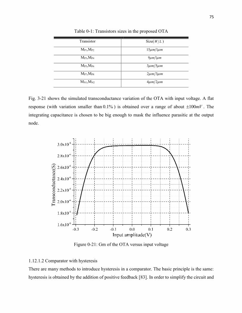
75
Table 0-1: Transistors sizes in the proposed OTA
Transistor Size(W L )
MP1,MP2 15 1m m
MP3,MP4 9 1m m
MP5,MP6 3 5m m
MP7,MP8 2 3m m
MN1,MN2 4 2m m
Fig. 3-21 shows the simulated transconductance variation of the OTA with input voltage. A flat
response (with variation smaller than 0.1% ) is obtained over a range of about 100mV . The
integrating capacitance is chosen to be big enough to mask the influence parasitic at the output
node.
Figure 0-21: Gm of the OTA versus input voltage
1.12.1.2 Comparator with hysteresis
There are many methods to introduce hysteresis in a comparator. The basic principle is the same:
hysteresis is obtained by the addition of positive feedback [83]. In order to simplify the circuit and
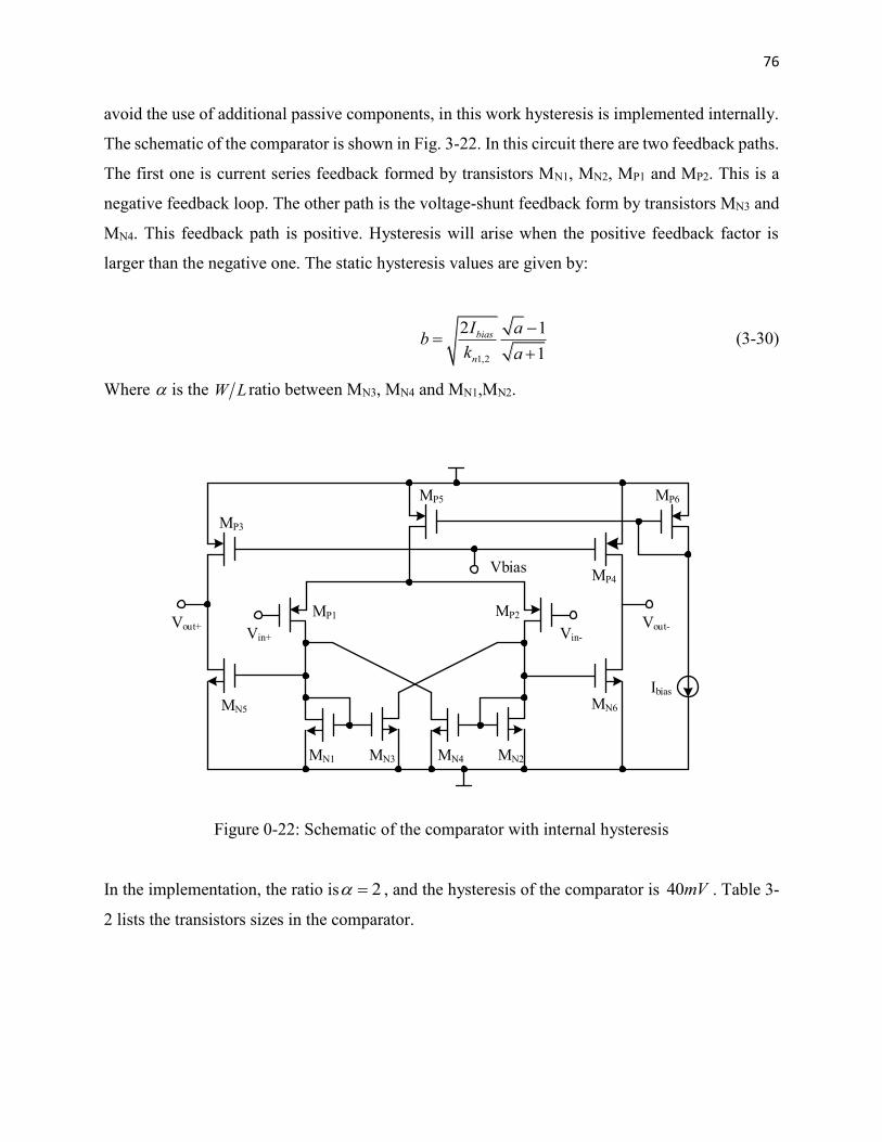
76
avoid the use of additional passive components, in this work hysteresis is implemented internally.
The schematic of the comparator is shown in Fig. 3-22. In this circuit there are two feedback paths.
The first one is current series feedback formed by transistors MN1, MN2, MP1 and MP2. This is a
negative feedback loop. The other path is the voltage-shunt feedback form by transistors MN3 and
MN4. This feedback path is positive. Hysteresis will arise when the positive feedback factor is
larger than the negative one. The static hysteresis values are given by:
1,2
2 1
1
bias
n
I ab
k a
(3-30)
Where is the W L ratio between MN3, MN4 and MN1,MN2.
Vin-Vin+
MP2MP1
MP4
MP3
MP5 MP6
Ibias
MN2MN4MN3MN1
MN5 MN6
Vout+ Vout-
Vbias
Figure 0-22: Schematic of the comparator with internal hysteresis
In the implementation, the ratio is 2 , and the hysteresis of the comparator is 40mV . Table 3-
2 lists the transistors sizes in the comparator.
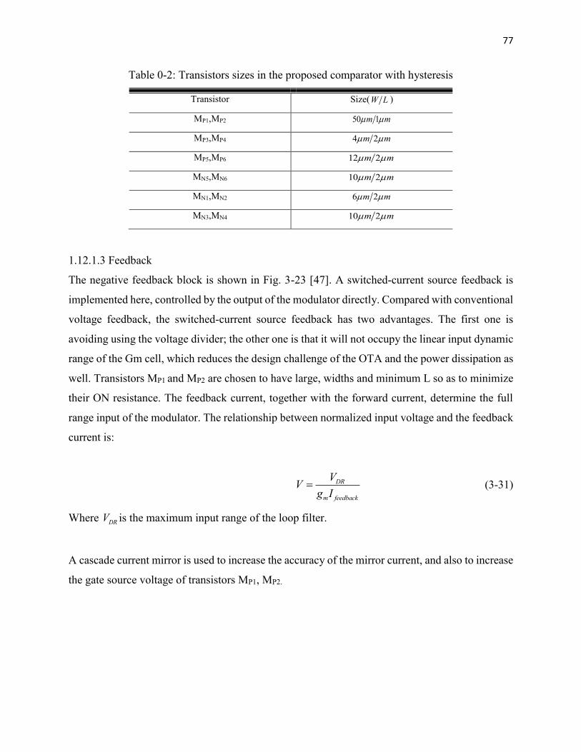
77
Table 0-2: Transistors sizes in the proposed comparator with hysteresis
Transistor Size(W L )
MP1,MP2 50 1m m
MP3,MP4 4 2m m
MP5,MP6 12 2m m
MN5,MN6 10 2m m
MN1,MN2 6 2m m
MN3,MN4 10 2m m
1.12.1.3 Feedback
The negative feedback block is shown in Fig. 3-23 [47]. A switched-current source feedback is
implemented here, controlled by the output of the modulator directly. Compared with conventional
voltage feedback, the switched-current source feedback has two advantages. The first one is
avoiding using the voltage divider; the other one is that it will not occupy the linear input dynamic
range of the Gm cell, which reduces the design challenge of the OTA and the power dissipation as
well. Transistors MP1 and MP2 are chosen to have large, widths and minimum L so as to minimize
their ON resistance. The feedback current, together with the forward current, determine the full
range input of the modulator. The relationship between normalized input voltage and the feedback
current is:
DR
m feedback
VV
g I (3-31)
Where DRV is the maximum input range of the loop filter.
A cascade current mirror is used to increase the accuracy of the mirror current, and also to increase
the gate source voltage of transistors MP1, MP2.
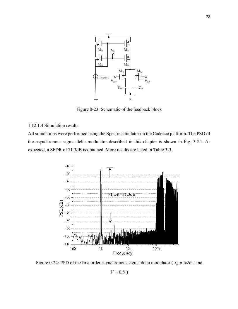
78
MP1
Ifeedback
Vout+
Cint Cint
Vout-
MP2
MP3 MP4
MP5 MP6
Vb
Figure 0-23: Schematic of the feedback block
1.12.1.4 Simulation results
All simulations were performed using the Spectre simulator on the Cadence platform. The PSD of
the asynchronous sigma delta modulator described in this chapter is shown in Fig. 3-24. As
expected, a SFDR of 71.3dB is obtained. More results are listed in Table 3-3.
Figure 0-24: PSD of the first order asynchronous sigma delta modulator ( 1inf kHz , and
0.8V )
79
Table 0-3: Simulation results for the ASDM
Parameter Results
cf 200kHz
Normalized input amplitude (V) 0.8
Bandwidth 3kHz
Input range 100mV
SFDR 71.3dB
Supply Voltage 1V
Power consumption 120 Watts
1.12.2 Time-to-digital converter based on vernier delay lines
1.12.2.1 Vernier delay line
As can be seen from Fig. 3-9 in the previous section, this configuration consists of a voltage
controlled delay line and time comparators. Details of the delay lines will be given first. Variable
delay lines elements fall into either of two categories: digitally-controlled delay elements and
voltage-controlled delay elements. The first type is realized by a variable length of delay elements.
The magnitude of the delay is determined by number of elements used in the chain. The resolution
of the delay chain is determined by the delay time of a single delay element. This kind of delay
chain can be easy realized by FPGAs. The second one is more appropriate for applications where
small, accurate, and precise value of delay is necessary. This is particularly true when sub-gate
delay resolution and ultra-low power of operation are required. Evidently, as there are the design
considerations in the realization of vernier delay lines, the analogueue controlled delay elements
are a more suitable design choice.
Fig. 3-25 shows the configuration of the voltage controlled delay lines. The delay time is controlled
by a control voltage controlV . There are two types of voltage controlled delay lines. The first one is
shunt capacitor, and the other one is current starved. For the shun-capacitor type of delay lines a
large value of the output capacitor is required in order to realize a large delay time. This takes up
a large silicon area. Moreover, the maximum delay and the range of voltage regulation are both
relatively small. The current starving delay line, because of its low power consumption and wide
range of voltage regulation, it is suitable for the implementation here. However, it suffers of
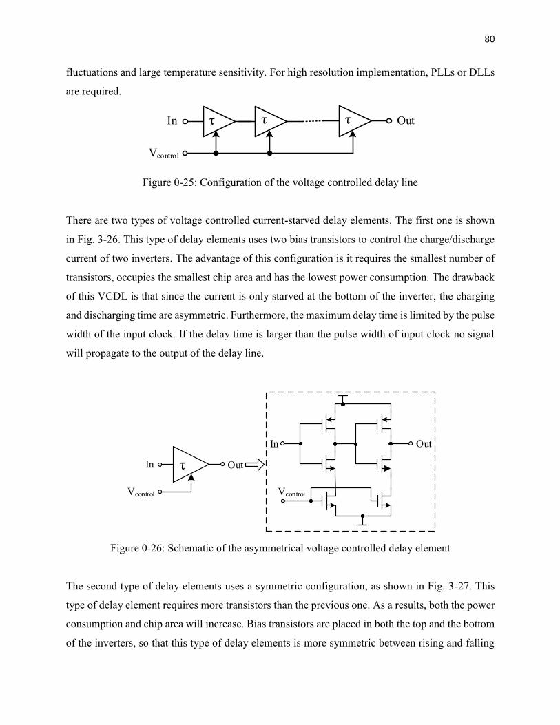
80
fluctuations and large temperature sensitivity. For high resolution implementation, PLLs or DLLs
are required.
τ τ τIn Out
Vcontrol
Figure 0-25: Configuration of the voltage controlled delay line
There are two types of voltage controlled current-starved delay elements. The first one is shown
in Fig. 3-26. This type of delay elements uses two bias transistors to control the charge/discharge
current of two inverters. The advantage of this configuration is it requires the smallest number of
transistors, occupies the smallest chip area and has the lowest power consumption. The drawback
of this VCDL is that since the current is only starved at the bottom of the inverter, the charging
and discharging time are asymmetric. Furthermore, the maximum delay time is limited by the pulse
width of the input clock. If the delay time is larger than the pulse width of input clock no signal
will propagate to the output of the delay line.
τ
VcontrolVcontrol
In Out
In Out
Figure 0-26: Schematic of the asymmetrical voltage controlled delay element
The second type of delay elements uses a symmetric configuration, as shown in Fig. 3-27. This
type of delay element requires more transistors than the previous one. As a results, both the power
consumption and chip area will increase. Bias transistors are placed in both the top and the bottom
of the inverters, so that this type of delay elements is more symmetric between rising and falling
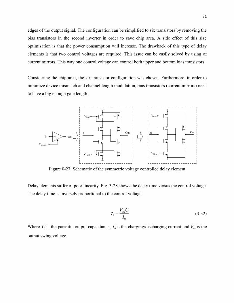
81
edges of the output signal. The configuration can be simplified to six transistors by removing the
bias transistors in the second inverter in order to save chip area. A side effect of this size
optimisation is that the power consumption will increase. The drawback of this type of delay
elements is that two control voltages are required. This issue can be easily solved by using of
current mirrors. This way one control voltage can control both upper and bottom bias transistors.
Considering the chip area, the six transistor configuration was chosen. Furthermore, in order to
minimize device mismatch and channel length modulation, bias transistors (current mirrors) need
to have a big enough gate length.
In Out
VNctrl
VPctrl
τ
Vcontrol
In Out
OutIn
VNctrl
VPctrl
Figure 0-27: Schematic of the symmetric voltage controlled delay element
Delay elements suffer of poor linearity. Fig. 3-28 shows the delay time versus the control voltage.
The delay time is inversely proportional to the control voltage:
0
0
swV C
I (3-32)
Where C is the parasitic output capacitance, 0I is the charging/discharging current and swV is the
output swing voltage.
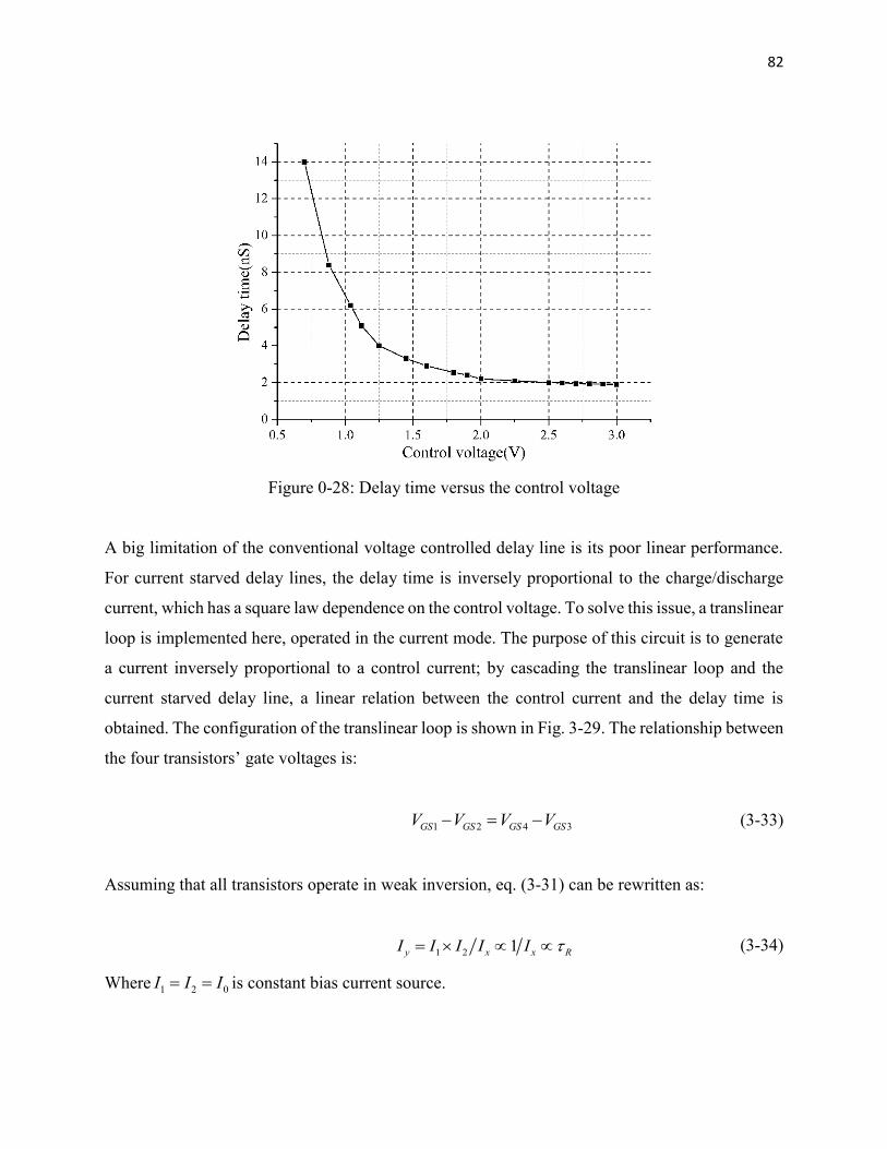
82
Figure 0-28: Delay time versus the control voltage
A big limitation of the conventional voltage controlled delay line is its poor linear performance.
For current starved delay lines, the delay time is inversely proportional to the charge/discharge
current, which has a square law dependence on the control voltage. To solve this issue, a translinear
loop is implemented here, operated in the current mode. The purpose of this circuit is to generate
a current inversely proportional to a control current; by cascading the translinear loop and the
current starved delay line, a linear relation between the control current and the delay time is
obtained. The configuration of the translinear loop is shown in Fig. 3-29. The relationship between
the four transistors’ gate voltages is:
1 2 4 3GS GS GS GSV V V V (3-33)
Assuming that all transistors operate in weak inversion, eq. (3-31) can be rewritten as:
1 2 1y x x RI I I I I (3-34)
Where 1 2 0I I I is constant bias current source.
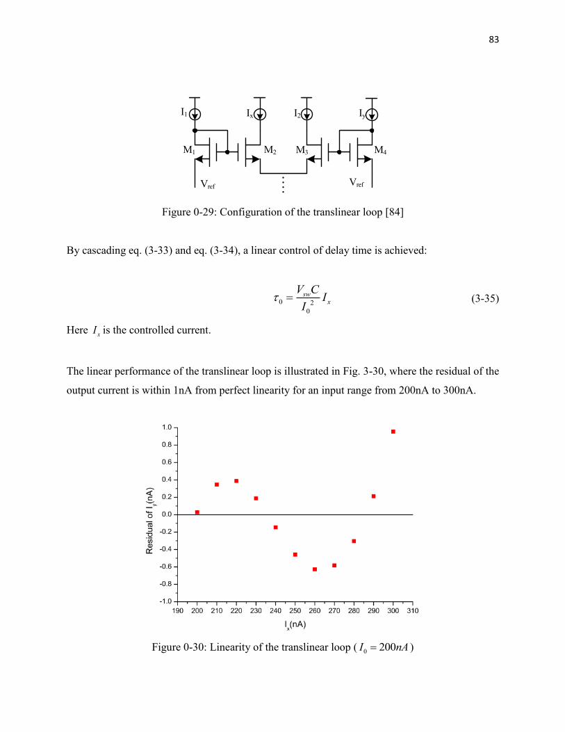
83
I1 I2Ix Iy
VrefVref
M1 M2 M3 M4
Figure 0-29: Configuration of the translinear loop [84]
By cascading eq. (3-33) and eq. (3-34), a linear control of delay time is achieved:
0 2
0
swx
V CI
I (3-35)
Here xI is the controlled current.
The linear performance of the translinear loop is illustrated in Fig. 3-30, where the residual of the
output current is within 1nA from perfect linearity for an input range from 200nA to 300nA.
Figure 0-30: Linearity of the translinear loop ( 0 200I nA )
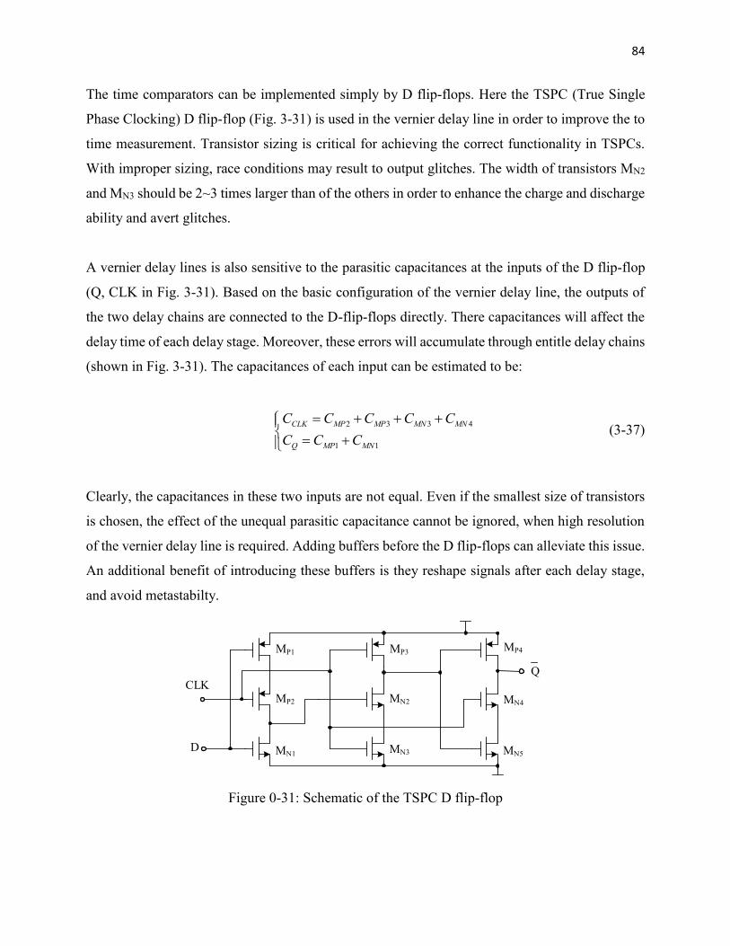
84
The time comparators can be implemented simply by D flip-flops. Here the TSPC (True Single
Phase Clocking) D flip-flop (Fig. 3-31) is used in the vernier delay line in order to improve the to
time measurement. Transistor sizing is critical for achieving the correct functionality in TSPCs.
With improper sizing, race conditions may result to output glitches. The width of transistors MN2
and MN3 should be 2~3 times larger than of the others in order to enhance the charge and discharge
ability and avert glitches.
A vernier delay lines is also sensitive to the parasitic capacitances at the inputs of the D flip-flop
(Q, CLK in Fig. 3-31). Based on the basic configuration of the vernier delay line, the outputs of
the two delay chains are connected to the D-flip-flops directly. There capacitances will affect the
delay time of each delay stage. Moreover, these errors will accumulate through entitle delay chains
(shown in Fig. 3-31). The capacitances of each input can be estimated to be:
2 3 3 4
1 1
CLK MP MP MN MN
Q MP MN
C C C C C
C C C
(3-37)
Clearly, the capacitances in these two inputs are not equal. Even if the smallest size of transistors
is chosen, the effect of the unequal parasitic capacitance cannot be ignored, when high resolution
of the vernier delay line is required. Adding buffers before the D flip-flops can alleviate this issue.
An additional benefit of introducing these buffers is they reshape signals after each delay stage,
and avoid metastabilty.
CLK
Q
D
MP1
MP2
MP3MP4
MN1
MN2
MN3
MN4
MN5
Figure 0-31: Schematic of the TSPC D flip-flop
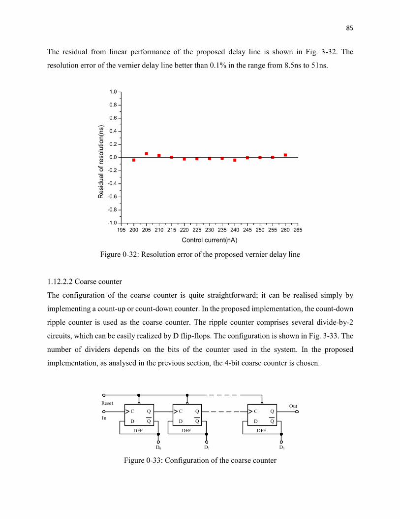
85
The residual from linear performance of the proposed delay line is shown in Fig. 3-32. The
resolution error of the vernier delay line better than 0.1% in the range from 8.5ns to 51ns.
Figure 0-32: Resolution error of the proposed vernier delay line
1.12.2.2 Coarse counter
The configuration of the coarse counter is quite straightforward; it can be realised simply by
implementing a count-up or count-down counter. In the proposed implementation, the count-down
ripple counter is used as the coarse counter. The ripple counter comprises several divide-by-2
circuits, which can be easily realized by D flip-flops. The configuration is shown in Fig. 3-33. The
number of dividers depends on the bits of the counter used in the system. In the proposed
implementation, as analysed in the previous section, the 4-bit coarse counter is chosen.
C
D
Q
QIn
Out
DFF
C
D
Q
Q
DFF
C
D
Q
Q
DFF
D0 D3D1
Reset
Figure 0-33: Configuration of the coarse counter
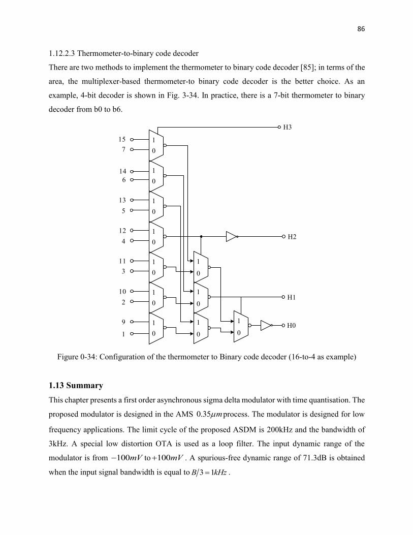
86
1.12.2.3 Thermometer-to-binary code decoder
There are two methods to implement the thermometer to binary code decoder [85]; in terms of the
area, the multiplexer-based thermometer-to binary code decoder is the better choice. As an
example, 4-bit decoder is shown in Fig. 3-34. In practice, there is a 7-bit thermometer to binary
decoder from b0 to b6.
0
1
0
1
0
1
0
1
0
1
0
1
1
0
1
0
1
0
1
0
0
1
1
H3
H1
H0
H2
9
2
10
3
4
5
6
7
11
12
13
14
15
Figure 0-34: Configuration of the thermometer to Binary code decoder (16-to-4 as example)
1.13 Summary
This chapter presents a first order asynchronous sigma delta modulator with time quantisation. The
proposed modulator is designed in the AMS 0.35 m process. The modulator is designed for low
frequency applications. The limit cycle of the proposed ASDM is 200kHz and the bandwidth of
3kHz. A special low distortion OTA is used as a loop filter. The input dynamic range of the
modulator is from 100mV to 100mV . A spurious-free dynamic range of 71.3dB is obtained
when the input signal bandwidth is equal to 3 1B kHz .

87
A new time quantiser for asynchronous sigma delta modulators is also presented. The circuit
implements a special coarse-fine time-to-digital converter to quantise the timing of the square
wave produced by asynchronous sigma delta modulators. This circuit converts the duty cycle to a
digital output. The proposed circuit measures the pulse width and the period separately by
implementing a special time-to-digital converter, which utilizes vernier delay lines. This structure
can achieve high resolution despite using a low sampling frequency.
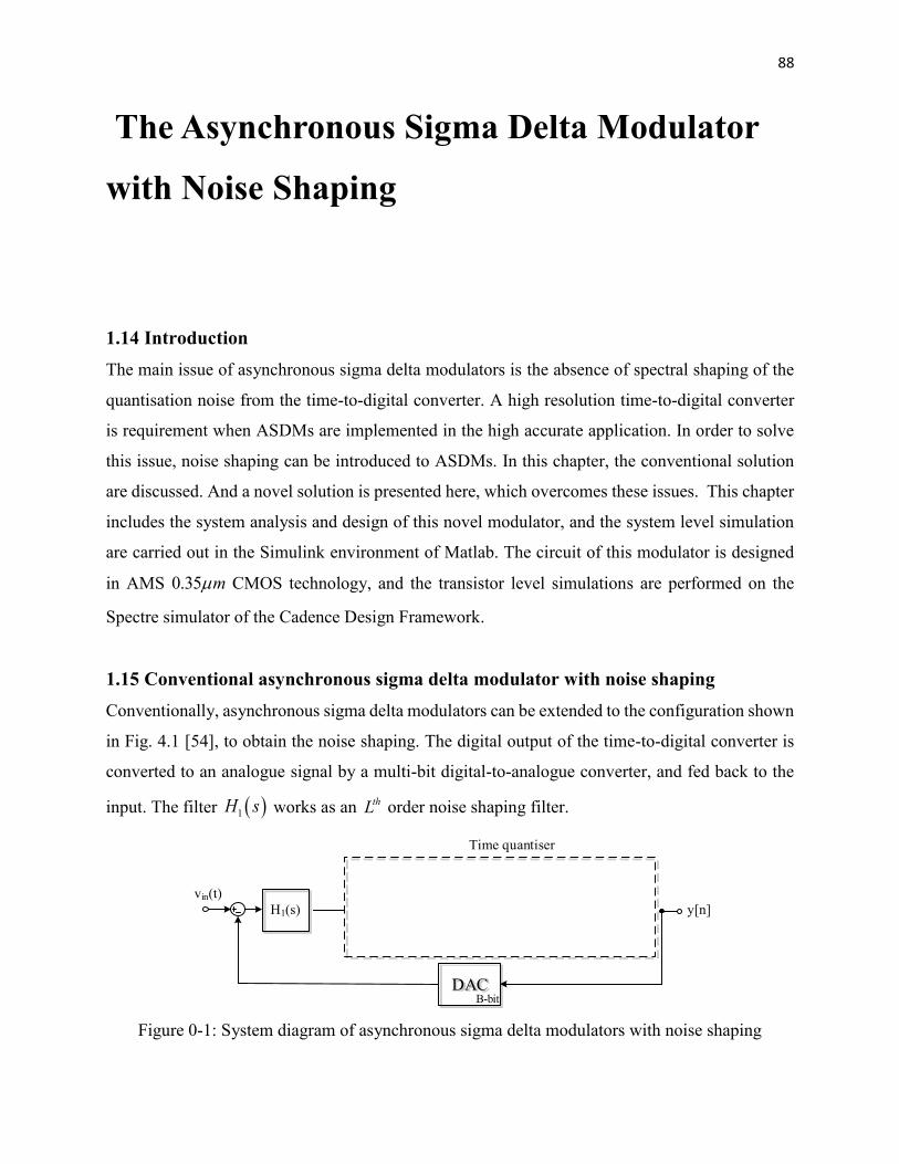
88
The Asynchronous Sigma Delta Modulator
with Noise Shaping
1.14 Introduction
The main issue of asynchronous sigma delta modulators is the absence of spectral shaping of the
quantisation noise from the time-to-digital converter. A high resolution time-to-digital converter
is requirement when ASDMs are implemented in the high accurate application. In order to solve
this issue, noise shaping can be introduced to ASDMs. In this chapter, the conventional solution
are discussed. And a novel solution is presented here, which overcomes these issues. This chapter
includes the system analysis and design of this novel modulator, and the system level simulation
are carried out in the Simulink environment of Matlab. The circuit of this modulator is designed
in AMS 0.35 m CMOS technology, and the transistor level simulations are performed on the
Spectre simulator of the Cadence Design Framework.
1.15 Conventional asynchronous sigma delta modulator with noise shaping
Conventionally, asynchronous sigma delta modulators can be extended to the configuration shown
in Fig. 4.1 [54], to obtain the noise shaping. The digital output of the time-to-digital converter is
converted to an analogue signal by a multi-bit digital-to-analogue converter, and fed back to the
input. The filter 1H s works as an thL order noise shaping filter.
c(t)vin(t)
TDCB-bit
Ts
y[n]
DACB-bit
H2(s)H1(s)
Time quantiser
Figure 0-1: System diagram of asynchronous sigma delta modulators with noise shaping
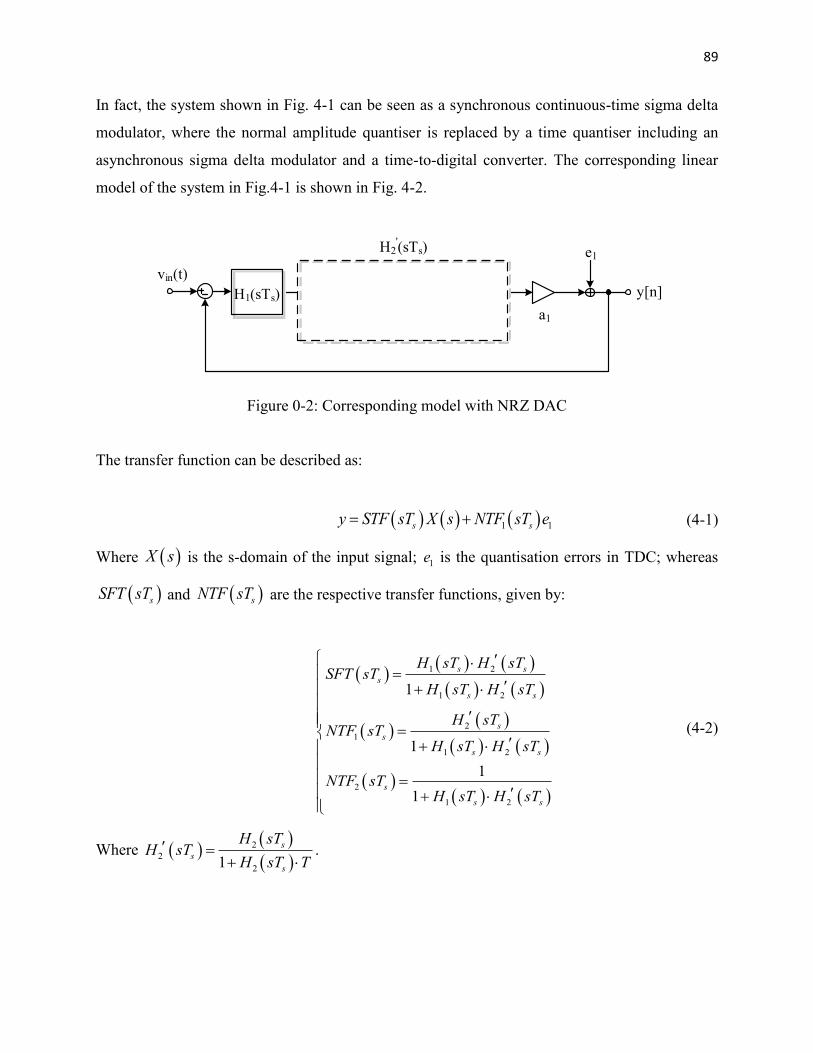
89
In fact, the system shown in Fig. 4-1 can be seen as a synchronous continuous-time sigma delta
modulator, where the normal amplitude quantiser is replaced by a time quantiser including an
asynchronous sigma delta modulator and a time-to-digital converter. The corresponding linear
model of the system in Fig.4-1 is shown in Fig. 4-2.
vin(t)
y[n]H2(s)H1(sTs)
a1
e1
T
H2'(sTs)
Figure 0-2: Corresponding model with NRZ DAC
The transfer function can be described as:
1 1s sy STF sT X s NTF sT e (4-1)
Where X s is the s-domain of the input signal; 1e is the quantisation errors in TDC; whereas
sSFT sT and sNTF sT are the respective transfer functions, given by:
1 2
1 2
2
1
1 2
2
1 2
1
1
1
1
s s
s
s s
s
s
s s
s
s s
H sT H sTSFT sT
H sT H sT
H sTNTF sT
H sT H sT
NTF sTH sT H sT
(4-2)
Where
2
2
21
s
s
s
H sTH sT
H sT T
.
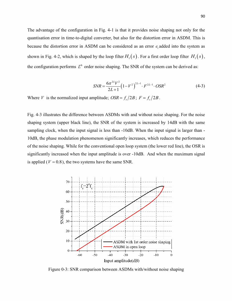
90
The advantage of the configuration in Fig. 4-1 is that it provides noise shaping not only for the
quantisation error in time-to-digital converter, but also for the distortion error in ASDM. This is
because the distortion error in ASDM can be considered as an error 1e added into the system as
shown in Fig. 4-2, which is shaped by the loop filter 1H s . For a first order loop filter 1H s ,
the configuration performs thL order noise shaping. The SNR of the system can be derived as:
2 2
2 12 2 1 26
12 1
LL
LVSNR V F OSR
L
(4-3)
Where V is the normalized input amplitude; 2sOSR f B ; 2cF f B .
Fig. 4-3 illustrates the difference between ASDMs with and without noise shaping. For the noise
shaping system (upper black line), the SNR of the system is increased by 14dB with the same
sampling clock, when the input signal is less than -10dB. When the input signal is larger than -
10dB, the phase modulation phenomenon significantly increases, which reduces the performance
of the noise shaping. While for the conventional open loop system (the lower red line), the OSR is
significantly increased when the input amplitude is over -10dB. And when the maximum signal
is applied ( 0.8V ), the two systems have the same SNR.
Figure 0-3: SNR comparison between ASDMs with/without noise shaping
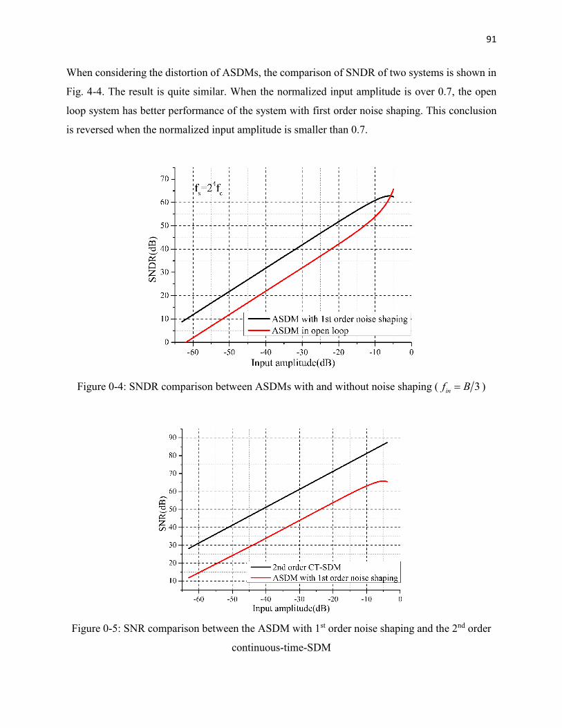
91
When considering the distortion of ASDMs, the comparison of SNDR of two systems is shown in
Fig. 4-4. The result is quite similar. When the normalized input amplitude is over 0.7, the open
loop system has better performance of the system with first order noise shaping. This conclusion
is reversed when the normalized input amplitude is smaller than 0.7.
Figure 0-4: SNDR comparison between ASDMs with and without noise shaping ( 3inf B )
Figure 0-5: SNR comparison between the ASDM with 1st order noise shaping and the 2nd order
continuous-time-SDM
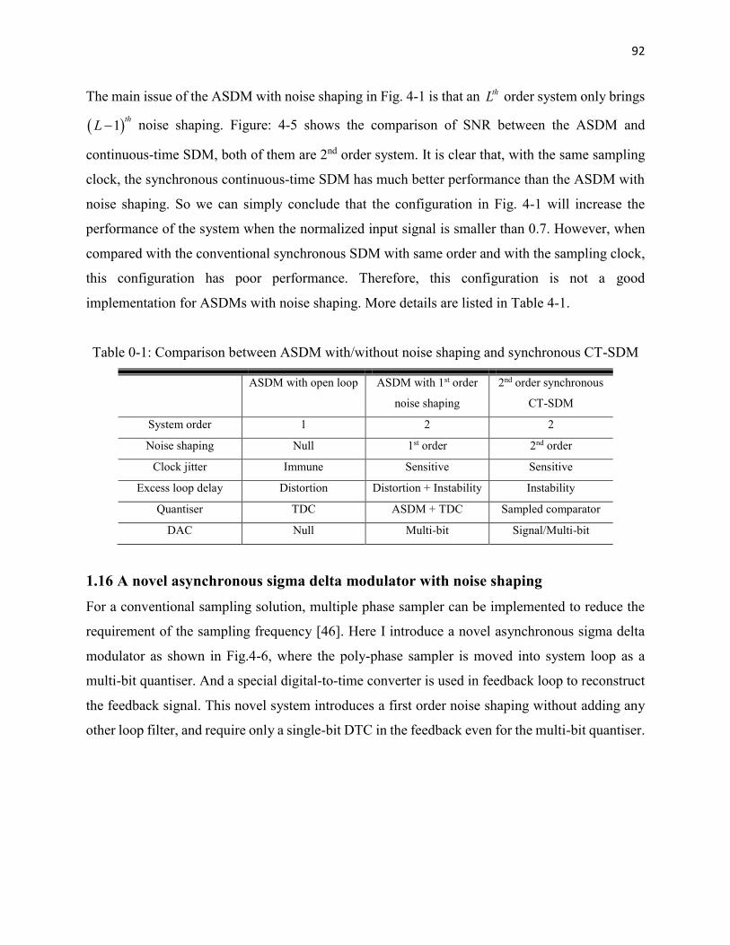
92
The main issue of the ASDM with noise shaping in Fig. 4-1 is that an thL order system only brings
1th
L noise shaping. Figure: 4-5 shows the comparison of SNR between the ASDM and
continuous-time SDM, both of them are 2nd order system. It is clear that, with the same sampling
clock, the synchronous continuous-time SDM has much better performance than the ASDM with
noise shaping. So we can simply conclude that the configuration in Fig. 4-1 will increase the
performance of the system when the normalized input signal is smaller than 0.7. However, when
compared with the conventional synchronous SDM with same order and with the sampling clock,
this configuration has poor performance. Therefore, this configuration is not a good
implementation for ASDMs with noise shaping. More details are listed in Table 4-1.
Table 0-1: Comparison between ASDM with/without noise shaping and synchronous CT-SDM
ASDM with open loop ASDM with 1st order
noise shaping
2nd order synchronous
CT-SDM
System order 1 2 2
Noise shaping Null 1st order 2nd order
Clock jitter Immune Sensitive Sensitive
Excess loop delay Distortion Distortion + Instability Instability
Quantiser TDC ASDM + TDC Sampled comparator
DAC Null Multi-bit Signal/Multi-bit
1.16 A novel asynchronous sigma delta modulator with noise shaping
For a conventional sampling solution, multiple phase sampler can be implemented to reduce the
requirement of the sampling frequency [46]. Here I introduce a novel asynchronous sigma delta
modulator as shown in Fig.4-6, where the poly-phase sampler is moved into system loop as a
multi-bit quantiser. And a special digital-to-time converter is used in feedback loop to reconstruct
the feedback signal. This novel system introduces a first order noise shaping without adding any
other loop filter, and require only a single-bit DTC in the feedback even for the multi-bit quantiser.
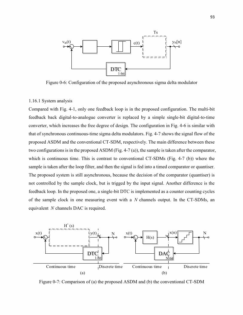
93
c(t)vin(t)
Ts
yN[n]
DTC1-bit
N
Figure 0-6: Configuration of the proposed asynchronous sigma delta modulator
1.16.1 System analysis
Compared with Fig. 4-1, only one feedback loop is in the proposed configuration. The multi-bit
feedback back digital-to-analogue converter is replaced by a simple single-bit digital-to-time
converter, which increases the free degree of design. The configuration in Fig. 4-6 is similar with
that of synchronous continuous-time sigma delta modulators. Fig. 4-7 shows the signal flow of the
proposed ASDM and the conventional CT-SDM, respectively. The main difference between these
two configurations is in the proposed ASDM (Fig. 4-7 (a)), the sample is taken after the comparator,
which is continuous time. This is contrast to conventional CT-SDMs (Fig. 4-7 (b)) where the
sample is taken after the loop filter, and then the signal is fed into a timed comparator or quantiser.
The proposed system is still asynchronous, because the decision of the comparator (quantiser) is
not controlled by the sample clock, but is trigged by the input signal. Another difference is the
feedback loop. In the proposed one, a single-bit DTC is implemented as a counter counting cycles
of the sample clock in one measuring event with a N channels output. In the CT-SDMs, an
equivalent N channels DAC is required.
x(t)
DTC1-bit
H(s)
H'(s)
y(t) N
Discrete timeDiscrete timeContinuous time
(a) (b)
x(t)
DACN-bit
H(s)
x(n) N
Continuous time
Figure 0-7: Comparison of (a) the proposed ASDM and (b) the conventional CT-SDM
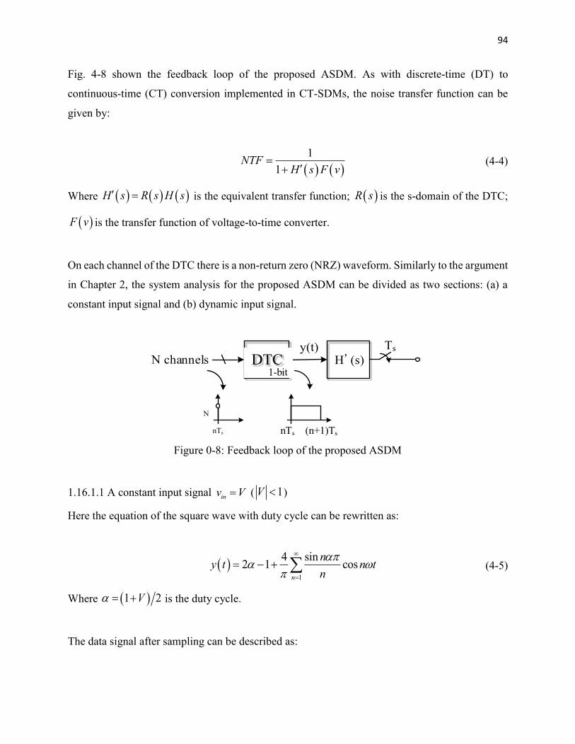
94
Fig. 4-8 shown the feedback loop of the proposed ASDM. As with discrete-time (DT) to
continuous-time (CT) conversion implemented in CT-SDMs, the noise transfer function can be
given by:
1
1NTF
H s F v
(4-4)
Where H s R s H s is the equivalent transfer function; R s is the s-domain of the DTC;
F v is the transfer function of voltage-to-time converter.
On each channel of the DTC there is a non-return zero (NRZ) waveform. Similarly to the argument
in Chapter 2, the system analysis for the proposed ASDM can be divided as two sections: (a) a
constant input signal and (b) dynamic input signal.
H'(s)N channelsy(t)
DTC1-bit
nTs nTs (n+1)Ts
Ts
N
Figure 0-8: Feedback loop of the proposed ASDM
1.16.1.1 A constant input signal inv V ( 1V )
Here the equation of the square wave with duty cycle can be rewritten as:
1
4 sin2 1 cos
n
ny t n t
n
(4-5)
Where 1 2V is the duty cycle.
The data signal after sampling can be described as:
95
0
0
N
k
y n y t t k
(4-6)
Where 0 sT M is the resolution of the delay chain; M is the length of the delay chain.
The digital-to-time converter here works as the simplicity digital-to-analogue converter, which is
assumed to have a zero-order-hold (ZOH) transfer function. For the NRZ waveform, the
reconstructed feedback signal can be obtained as:
0
0
N
k
y t y t t k R t
(4-7)
Where 0R t u t u t .
By inserting eq. (4-6), the feedback signal is:
0 0
0 1
4 sin2 1 cos
N
k n
ny t n k R t k
n
(4-8)
According to eq. (2-13), the output of the loop filter can be written as:
0 0
0 1
2 1 Re 0
4 sinRe cos Im sin
N
k n
c t V H
nH n n k H n n k
n
(4-9)
Where H is Fourier form of the loop filter.
Slightly different with eq. (2-15), the boundary conditions here can be shown to be:
1 0 1 1 0 1
2 0 1 2 0 2
1,
2
1,
2
t mT T k c t b
t mT T k c t b
(4-10)
96
Where 00, is the quantisation error.
Inserting the boundary conditions will result in:
0 0
1 0 0
2
0 0
1 0 0
2 sin 22 1 Re cos 2 Im sin 2
Re 0
sinRe sin 2 Im cos 2
4
n
n
nV H n n H n n
n H T T
n bH n n H n n
n T T
(4-11)
Where
0 1 0 0 1
0
cos cos cos 2n k n t n nT
0 2 0 0 2
0
cos cos cos 2n k n t n nT
0 1 0 0 1
0
sin sin sin 2n k n t n nT
0 2 0 0 2
0
sin sin sin 2n k n t n nT
and 0T is the output frequency of the ASDM.
Clearly, when 0 0 , the quantisation error becomes zero, the equation above becomes that of
the conventional ASDM given in Chapter 2. Inserting 1 2V into eq. (4-11) gives:
0 0
1 0 0
1 sin22 1 Re cos 2 Im sin 2
Re 0
n
n
n VV H n n H n n
n H T T
(4-12)
For a loop filter with non-zero single pole is:
97
a
Hj p
(4-13)
Inserting eq. (4-13) to eq. (4-12) will results in:
222 1 1
3V V
(4-14)
Where 0 0
2 sin 24
p
T
.
Assuming that 0 1p , the duty cycle is quasi proportional to the normalized amplitude of the
input signal, which is the same as the conclusion obtained in Chapter 2. For an ideal integrator
1
Hj
( 0p ), becomes zero, and the right hand of eq. (4-14) becomes V .
Therefore, for a constant input V ( 1V ) signal, the duty cycle of the proposed ASDM is
proportional to the input, as it the case with the conventional ASDM.
1.16.1.2 Dynamic input signal cosinv V t ( 1V )
Similar to Chapter 2, the same assumption is applied: the variation of the input signal is much
slower than the limit cycle frequency. Hence the equation of the input signal can be rewritten as:
0
0 0 0
cos cos cosM M N
in m mm m k
v V t V T V k
(4-15)
During the period of 1m mT t T , the output of the loop filter c t can be given by:
0 0
0
0 0
0 1
cos 2 1 Re cos Im sin
4 sinRe cos Im sin
N
mmk
N
k n
c t V T H k H k
nH n n k H n n k
n
(4-16)
98
By inserting the boundary conditions (eq. (4-10)), the following equations can be obtained:
1
2
1
sin 22cos 2 1
Re cos
Re cos 2 Im sin 2
sin4Re sin 2 Im cos 2
mm m
n m
m m
m m
mm m
n m m
nV T
n H T
H n n H n nT T
nH n n H n n b
n T T
(4-17)
Where 1 0 2 0 1, ,m mk k T T ; 1 0 2 0cos cos cos mk k T ; 1 0 2 0sin sin sin mk k T
( m ).
Again, insertion of cos 1 2m mV T , results in:
1
1 sin cos2cos 2 1
Re
Re cos 2 Im sin 2
n
m
m m
n
m m
m m
n V TV T
n H
H n n H n nT T
(4-18)
For an ideal integrator filter, eq. (4-18) can be rewritten as:
232 1 cos cos cos3
24 24m m m m
AV T V T AV T
(4-19)
Where
2
12 sin 2
4m m
AF T
; m
mF
.
It is interesting to notice that, for the proposed ASDM, the most significant distortion is still the
third order harmonic distortion, shown in eq. (4-20). Similar to the effect of the propagation delay
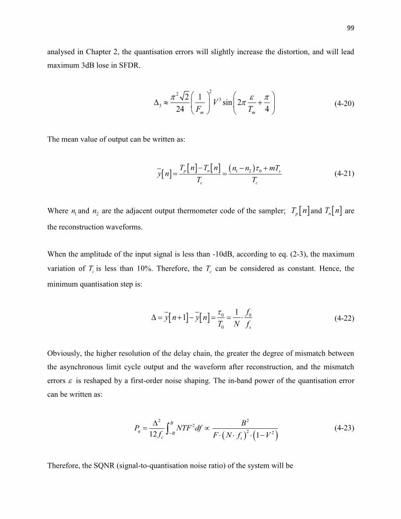
99
analysed in Chapter 2, the quantisation errors will slightly increase the distortion, and will lead
maximum 3dB lose in SFDR.
22
3
3
2 1sin 2
24 4m m
VF T
(4-20)
The mean value of output can be written as:
1 2 0p n s
c c
T n T n n n mTy n
T T
(4-21)
Where 1n and 2n are the adjacent output thermometer code of the sampler; pT n and nT n are
the reconstruction waveforms.
When the amplitude of the input signal is less than -10dB, according to eq. (2-3), the maximum
variation of cT is less than 10%. Therefore, the cT can be considered as constant. Hence, the
minimum quantisation step is:
0 0
0
11
s
fy n y n
T N f
(4-22)
Obviously, the higher resolution of the delay chain, the greater the degree of mismatch between
the asynchronous limit cycle output and the waveform after reconstruction, and the mismatch
errors is reshaped by a first-order noise shaping. The in-band power of the quantisation error
can be written as:
2 22
2 212 1
B
qB
c s
BP NTF df
f F N f V
(4-23)
Therefore, the SQNR (signal-to-quantisation noise ratio) of the system will be
100
2
2 21sN fSQNR V F V
B
(4-24)
Where 2cF f B ; B is the signal bandwidth; N is length of the delay chain.
Therefore, the SNDR of the system can be derived as:
2
2
3,q
VSNDR
Sum p
(4-25)
Fig. 4-9 shows the estimation of SNDR for both ASDM with/without noise shaping. Note that with
benefits of the noise shaping, the SNDR is significantly improved when the input signal is smaller
than -10dB, where the quantisation errors are dominant. The improvement is approximate 25dB.
While when the input signal is larger then -10dB, the SNDR is slightly dropped off. This is because
the distortion is increased significantly.
Figure 0-9: Estimation of achieved SNDR of conventional and proposed ASDM
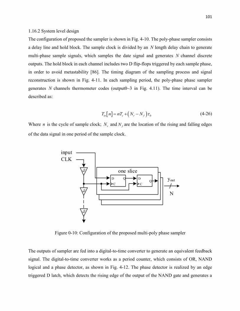
101
1.16.2 System level design
The configuration of proposed the sampler is shown in Fig. 4-10. The poly-phase sampler consists
a delay line and hold block. The sample clock is divided by an N length delay chain to generate
multi-phase sample signals, which samples the date signal and generates N channel discrete
outputs. The hold block in each channel includes two D flip-flops triggered by each sample phase,
in order to avoid metastability [86]. The timing diagram of the sampling process and signal
reconstruction is shown in Fig. 4-11. In each sampling period, the poly-phase phase sampler
generates N channels thermometer codes (output0~3 in Fig. 4.11). The time interval can be
described as:
0in s r fT n nT N N (4-26)
Where n is the cycle of sample clock; rN andfN are the location of the rising and falling edges
of the data signal in one period of the sample clock.
input
CLK
C
D Q
C
DQ
τ 0τ 0
τ 0
one slice
yout
N
Figure 0-10: Configuration of the proposed multi-poly phase sampler
The outputs of sampler are fed into a digital-to-time converter to generate an equivalent feedback
signal. The digital-to-time converter works as a period counter, which consists of OR, NAND
logical and a phase detector, as shown in Fig. 4-12. The phase detector is realized by an edge
triggered D latch, which detects the rising edge of the output of the NAND gate and generates a
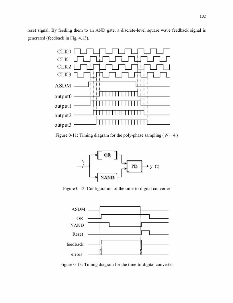
102
reset signal. By feeding them to an AND gate, a discrete-level square wave feedback signal is
generated (feedback in Fig, 4.13).
CLK0
ASDM
output0
output1
output2
output3
CLK1
CLK2
CLK3
Figure 0-11: Timing diagram for the poly-phase sampling ( 4N )
OR
N
NAND
PD y'(t)
Figure 0-12: Configuration of the time-to-digital converter
OR
NAND
feedback
Reset
ASDM
errors
Figure 0-13: Timing diagram for the time-to-digital converter
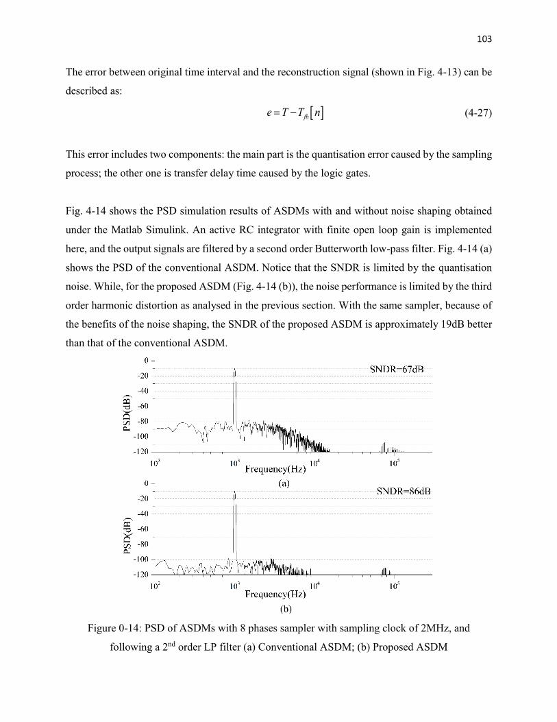
103
The error between original time interval and the reconstruction signal (shown in Fig. 4-13) can be
described as:
fbe T T n (4-27)
This error includes two components: the main part is the quantisation error caused by the sampling
process; the other one is transfer delay time caused by the logic gates.
Fig. 4-14 shows the PSD simulation results of ASDMs with and without noise shaping obtained
under the Matlab Simulink. An active RC integrator with finite open loop gain is implemented
here, and the output signals are filtered by a second order Butterworth low-pass filter. Fig. 4-14 (a)
shows the PSD of the conventional ASDM. Notice that the SNDR is limited by the quantisation
noise. While, for the proposed ASDM (Fig. 4-14 (b)), the noise performance is limited by the third
order harmonic distortion as analysed in the previous section. With the same sampler, because of
the benefits of the noise shaping, the SNDR of the proposed ASDM is approximately 19dB better
than that of the conventional ASDM.
Figure 0-14: PSD of ASDMs with 8 phases sampler with sampling clock of 2MHz, and
following a 2nd order LP filter (a) Conventional ASDM; (b) Proposed ASDM
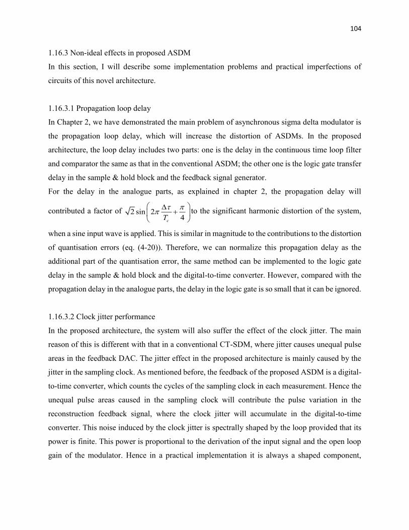
104
1.16.3 Non-ideal effects in proposed ASDM
In this section, I will describe some implementation problems and practical imperfections of
circuits of this novel architecture.
1.16.3.1 Propagation loop delay
In Chapter 2, we have demonstrated the main problem of asynchronous sigma delta modulator is
the propagation loop delay, which will increase the distortion of ASDMs. In the proposed
architecture, the loop delay includes two parts: one is the delay in the continuous time loop filter
and comparator the same as that in the conventional ASDM; the other one is the logic gate transfer
delay in the sample & hold block and the feedback signal generator.
For the delay in the analogue parts, as explained in chapter 2, the propagation delay will
contributed a factor of 2 sin 24cT
to the significant harmonic distortion of the system,
when a sine input wave is applied. This is similar in magnitude to the contributions to the distortion
of quantisation errors (eq. (4-20)). Therefore, we can normalize this propagation delay as the
additional part of the quantisation error, the same method can be implemented to the logic gate
delay in the sample & hold block and the digital-to-time converter. However, compared with the
propagation delay in the analogue parts, the delay in the logic gate is so small that it can be ignored.
1.16.3.2 Clock jitter performance
In the proposed architecture, the system will also suffer the effect of the clock jitter. The main
reason of this is different with that in a conventional CT-SDM, where jitter causes unequal pulse
areas in the feedback DAC. The jitter effect in the proposed architecture is mainly caused by the
jitter in the sampling clock. As mentioned before, the feedback of the proposed ASDM is a digital-
to-time converter, which counts the cycles of the sampling clock in each measurement. Hence the
unequal pulse areas caused in the sampling clock will contribute the pulse variation in the
reconstruction feedback signal, where the clock jitter will accumulate in the digital-to-time
converter. This noise induced by the clock jitter is spectrally shaped by the loop provided that its
power is finite. This power is proportional to the derivation of the input signal and the open loop
gain of the modulator. Hence in a practical implementation it is always a shaped component,
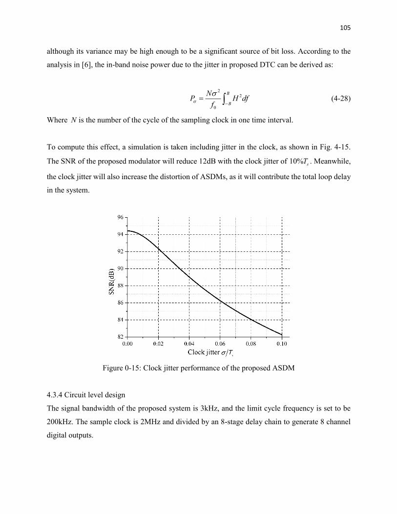
105
although its variance may be high enough to be a significant source of bit loss. According to the
analysis in [6], the in-band noise power due to the jitter in proposed DTC can be derived as:
2
2
0
B
B
NP H df
f
(4-28)
Where N is the number of the cycle of the sampling clock in one time interval.
To compute this effect, a simulation is taken including jitter in the clock, as shown in Fig. 4-15.
The SNR of the proposed modulator will reduce 12dB with the clock jitter of 10% sT . Meanwhile,
the clock jitter will also increase the distortion of ASDMs, as it will contribute the total loop delay
in the system.
Figure 0-15: Clock jitter performance of the proposed ASDM
4.3.4 Circuit level design
The signal bandwidth of the proposed system is 3kHz, and the limit cycle frequency is set to be
200kHz. The sample clock is 2MHz and divided by an 8-stage delay chain to generate 8 channel
digital outputs.
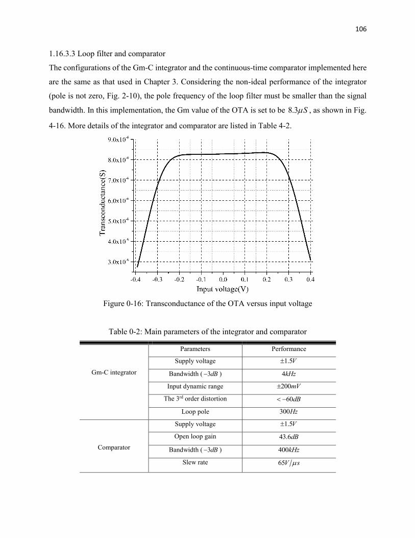
106
1.16.3.3 Loop filter and comparator
The configurations of the Gm-C integrator and the continuous-time comparator implemented here
are the same as that used in Chapter 3. Considering the non-ideal performance of the integrator
(pole is not zero, Fig. 2-10), the pole frequency of the loop filter must be smaller than the signal
bandwidth. In this implementation, the Gm value of the OTA is set to be 8.3 S , as shown in Fig.
4-16. More details of the integrator and comparator are listed in Table 4-2.
Figure 0-16: Transconductance of the OTA versus input voltage
Table 0-2: Main parameters of the integrator and comparator
Gm-C integrator
Parameters Performance
Supply voltage 1.5V
Bandwidth ( 3dB ) 4kHz
Input dynamic range 200mV
The 3rd order distortion 60dB
Loop pole 300Hz
Comparator
Supply voltage 1.5V
Open loop gain 43.6dB
Bandwidth ( 3dB ) 400kHz
Slew rate 65V s
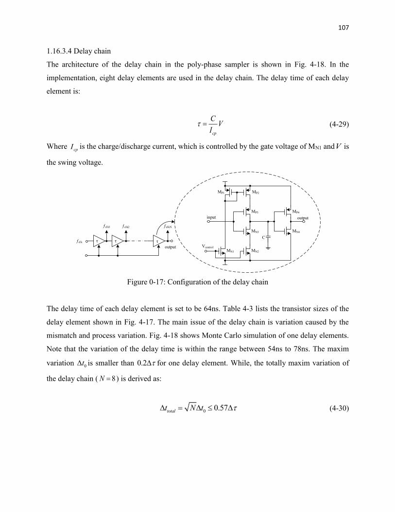
107
1.16.3.4 Delay chain
The architecture of the delay chain in the poly-phase sampler is shown in Fig. 4-18. In the
implementation, eight delay elements are used in the delay chain. The delay time of each delay
element is:
cp
CV
I (4-29)
Where cpI is the charge/discharge current, which is controlled by the gate voltage of MN1 andV is
the swing voltage.
MP1
output
Vcontrol
MP2
MP3 MP4
MN4MN3
MN2MN1
input
Cƒclk τ τ
output
τ
ƒclk1 ƒclk2 ƒclkN
Figure 0-17: Configuration of the delay chain
The delay time of each delay element is set to be 64ns. Table 4-3 lists the transistor sizes of the
delay element shown in Fig. 4-17. The main issue of the delay chain is variation caused by the
mismatch and process variation. Fig. 4-18 shows Monte Carlo simulation of one delay elements.
Note that the variation of the delay time is within the range between 54ns to 78ns. The maxim
variation 0t is smaller than 0.2 for one delay element. While, the totally maxim variation of
the delay chain ( 8N ) is derived as:
0 0.57totalt N t (4-30)
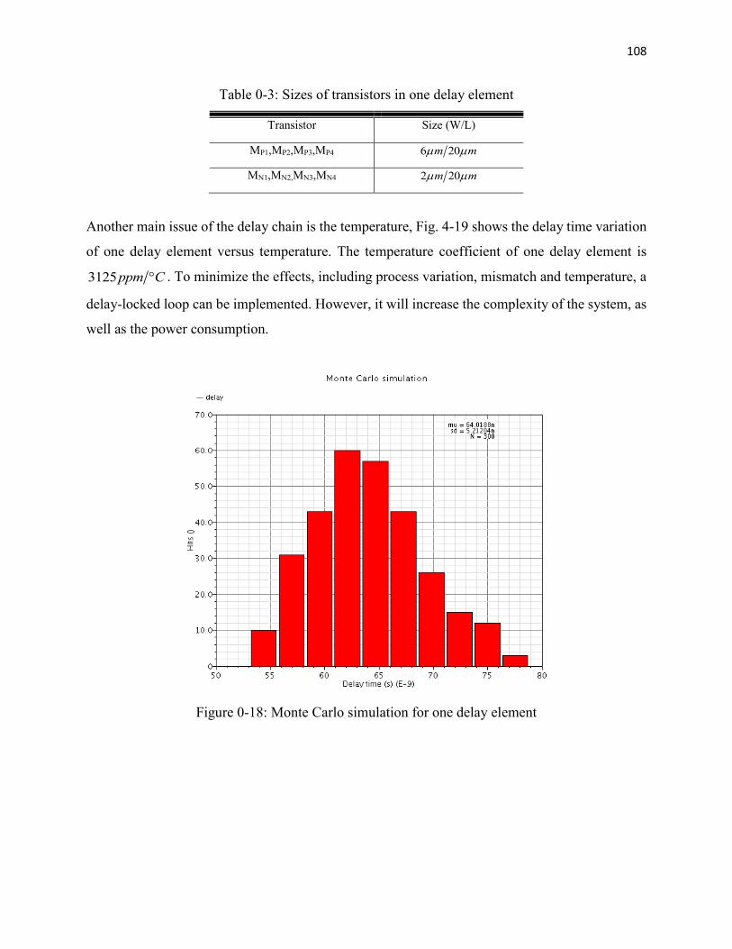
108
Table 0-3: Sizes of transistors in one delay element
Transistor Size (W/L)
MP1,MP2,MP3,MP4 6 20m m
MN1,MN2,MN3,MN4 2 20m m
Another main issue of the delay chain is the temperature, Fig. 4-19 shows the delay time variation
of one delay element versus temperature. The temperature coefficient of one delay element is
3125ppm C . To minimize the effects, including process variation, mismatch and temperature, a
delay-locked loop can be implemented. However, it will increase the complexity of the system, as
well as the power consumption.
Figure 0-18: Monte Carlo simulation for one delay element
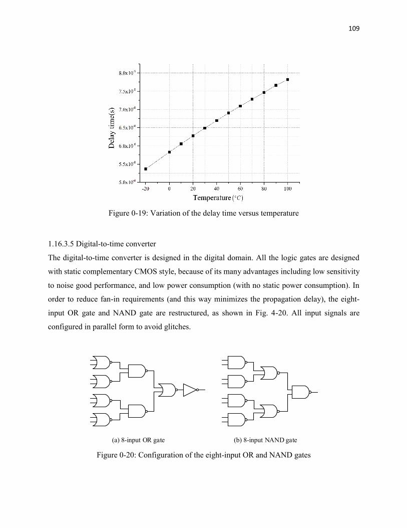
109
Figure 0-19: Variation of the delay time versus temperature
1.16.3.5 Digital-to-time converter
The digital-to-time converter is designed in the digital domain. All the logic gates are designed
with static complementary CMOS style, because of its many advantages including low sensitivity
to noise good performance, and low power consumption (with no static power consumption). In
order to reduce fan-in requirements (and this way minimizes the propagation delay), the eight-
input OR gate and NAND gate are restructured, as shown in Fig. 4-20. All input signals are
configured in parallel form to avoid glitches.
(a) 8-input OR gate (b) 8-input NAND gate
Figure 0-20: Configuration of the eight-input OR and NAND gates
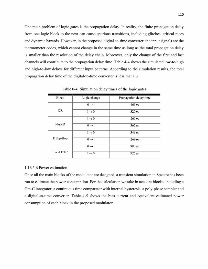
110
One main problem of logic gates is the propagation delay. In reality, the finite propagation delay
from one logic block to the next can cause spurious transitions, including glitches, critical races
and dynamic hazards. However, in the proposed digital-to-time converter, the input signals are the
thermometer codes, which cannot change in the same time as long as the total propagation delay
is smaller than the resolution of the delay chain. Moreover, only the change of the first and last
channels will contribute to the propagation delay time. Table 4-4 shows the simulated low-to-high
and high-to-low delays for different input patterns. According to the simulation results, the total
propagation delay time of the digital-to-time converter is less than1ns
Table 0-4: Simulation delay times of the logic gates
Block Logic change Propagation delay time
OR
0 1 465ps
1 0 320ps
NAND
1 0 265ps
0 1 365ps
D flip-flop
1 0 349ps
0 1 269ps
Total DTC
0 1 880ps
1 0 925ps
1.16.3.6 Power estimation
Once all the main blocks of the modulator are designed, a transient simulation in Spectre has been
run to estimate the power consumption. For the calculation we take in account blocks, including a
Gm-C integrator, a continuous time comparator with internal hysteresis, a poly-phase sampler and
a digital-to-time converter. Table 4-5 shows the bias current and equivalent estimated power
consumption of each block in the proposed modulator.
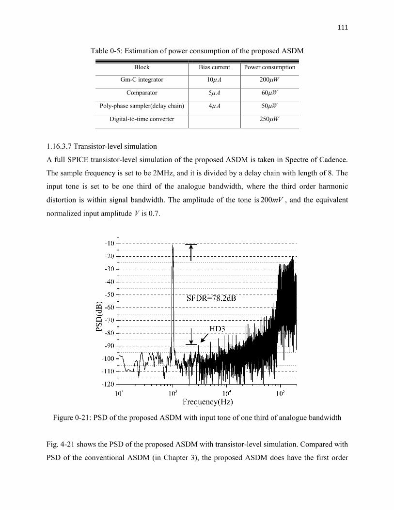
111
Table 0-5: Estimation of power consumption of the proposed ASDM
Block Bias current Power consumption
Gm-C integrator 10 A 200 W
Comparator 5 A 60 W
Poly-phase sampler(delay chain) 4 A 50 W
Digital-to-time converter 250 W
1.16.3.7 Transistor-level simulation
A full SPICE transistor-level simulation of the proposed ASDM is taken in Spectre of Cadence.
The sample frequency is set to be 2MHz, and it is divided by a delay chain with length of 8. The
input tone is set to be one third of the analogue bandwidth, where the third order harmonic
distortion is within signal bandwidth. The amplitude of the tone is 200mV , and the equivalent
normalized input amplitude V is 0.7.
Figure 0-21: PSD of the proposed ASDM with input tone of one third of analogue bandwidth
Fig. 4-21 shows the PSD of the proposed ASDM with transistor-level simulation. Compared with
PSD of the conventional ASDM (in Chapter 3), the proposed ASDM does have the first order
112
noise shaping. The SNDR of the modulator is 78.2dB, as expected, which is limited by the third
order harmonic distortion.
1.17 Summary
In this chapter, the conventional solution to implement noise shaping in asynchronous sigma delta
modulators has been discussed. By adding an additional loop filter and a multi-bit DAC, noise
shaping is added into asynchronous sigma delta modulators. However, it is not a recommend
solution, because it not only occupies a very large chip area and high power consumption, but also
suffers many non-ideal effects, such as stability, non-linearity and clock jitter in multi-bit DAC.
To solve these issues, a novel asynchronous sigma delta modulator with noise shaping has been
presented. The sampler is applied after the comparator, and feedback loop is realized by the digital-
to-time converter. This novel modulator still belongs to asynchronous class, since the decision of
the comparator is still determined by the input signal amplitude and not the clock. The proposed
modulator is sampled by a 2MHz clock divided by an 8-stage delay chain. According to the
simulation performed with the Spectre simulator of Cadence, the proposed modulator can achieved
peak SNDR of 78.2dB, which is 22dB better than the conventional asynchronous sigma delta
modulator with same sampling frequency.
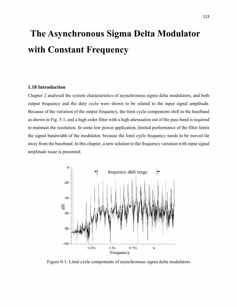
113
The Asynchronous Sigma Delta Modulator
with Constant Frequency
1.18 Introduction
Chapter 2 analysed the system characteristics of asynchronous sigma delta modulators, and both
output frequency and the duty cycle were shown to be related to the input signal amplitude.
Because of the variation of the output frequency, the limit cycle components shift to the baseband
as shown in Fig. 5-1, and a high order filter with a high attenuation out of the pass band is required
to maintain the resolution. In some low power application, limited performance of the filter limits
the signal bandwidth of the modulator, because the limit cycle frequency needs to be moved far
away from the baseband. In this chapter, a new solution to the frequency variation with input signal
amplitude issue is presented.
Figure 0-1: Limit cycle components of asynchronous sigma delta modulators
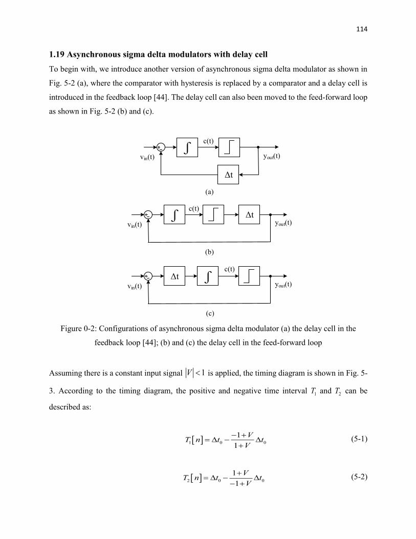
114
1.19 Asynchronous sigma delta modulators with delay cell
To begin with, we introduce another version of asynchronous sigma delta modulator as shown in
Fig. 5-2 (a), where the comparator with hysteresis is replaced by a comparator and a delay cell is
introduced in the feedback loop [44]. The delay cell can also been moved to the feed-forward loop
as shown in Fig. 5-2 (b) and (c).
vin(t) yout(t)
c(t)ʃ
Δt
vin(t) yout(t)
c(t)ʃ Δt
(a)
vin(t) yout(t)
c(t)Δt ʃ
(b)
(c)
Figure 0-2: Configurations of asynchronous sigma delta modulator (a) the delay cell in the
feedback loop [44]; (b) and (c) the delay cell in the feed-forward loop
Assuming there is a constant input signal 1V is applied, the timing diagram is shown in Fig. 5-
3. According to the timing diagram, the positive and negative time interval 1T and 2T can be
described as:
1 0 0
1
1
VT n t t
V (5-1)
2 0 0
1
1
VT n t t
V (5-2)
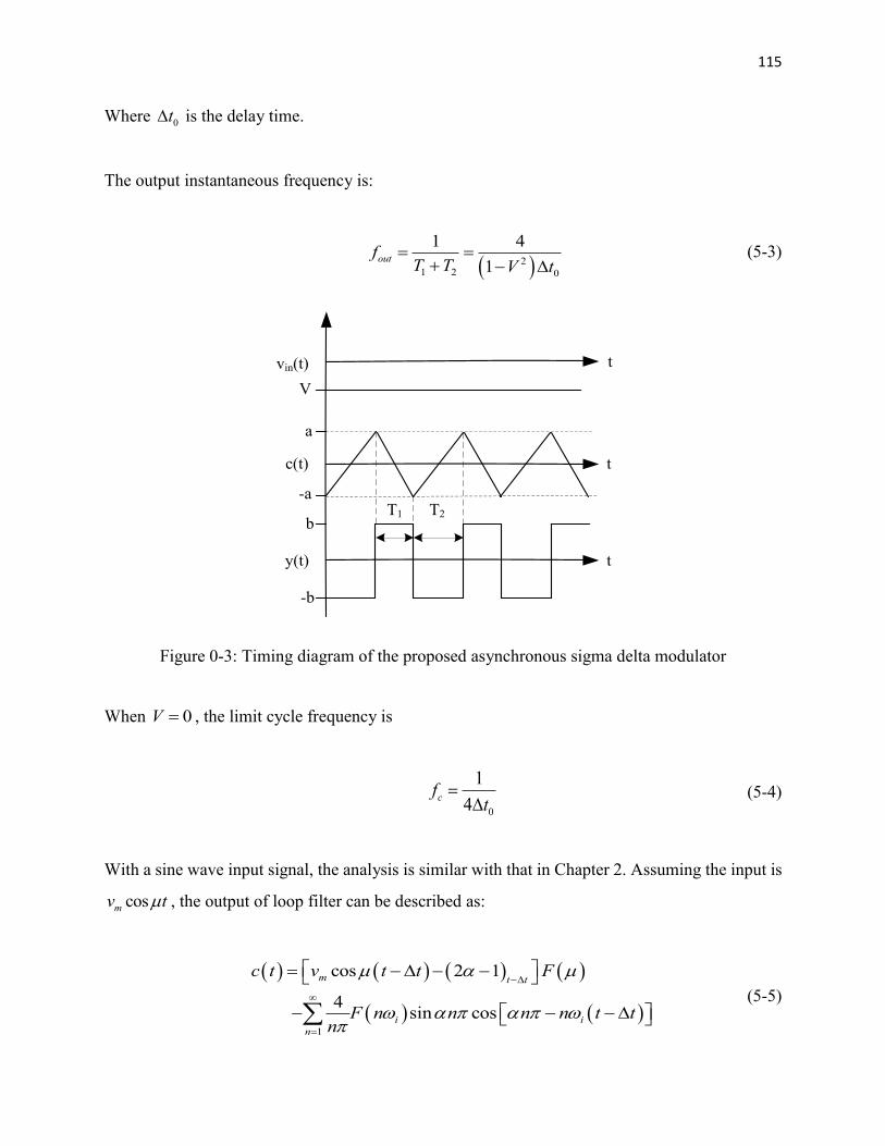
115
Where 0t is the delay time.
The output instantaneous frequency is:
21 2 0
1 4
1
outf
T T V t (5-3)
b
a
-a
-b
t
t
T1 T2
c(t)
y(t)
tvin(t)
V
Figure 0-3: Timing diagram of the proposed asynchronous sigma delta modulator
When 0V , the limit cycle frequency is
0
1
4
cf
t (5-4)
With a sine wave input signal, the analysis is similar with that in Chapter 2. Assuming the input is
cosmv t , the output of loop filter can be described as:
1
cos 2 1
4sin cos
m t t
i i
n
c t v t t F
F n n n n t tn
(5-5)
116
The boundary conditions are:
10
0
k
k
c t at t T kT
c t at t kT (5-6)
Inserting eq. (5-6) to eq. (5-5) conditions will result:
1
2 1 cos
4sin cos
m
i i
n
c t v F t t
F n n n n t tn
(5-7)
Here we consider 1t and use the same approximation implemented in chapter 2:
1 2 1 k k k
i
T kT k T k T T
(5-8)
and
1cos cos 1 k kT kT kT (5-9)
Based on the conditions (5-6), two equations can be obtained:
1
1 0
22 1 Re sin cos
2
i im i
n
F n nv n T
n F
(5-10)
2
1 0
1 1
4sin sin
2
2 1 sin sin2 2
i i
n
m k
F n nn
n F
T Tv kT t
(5-11)
It is clear to see that eq. (5-10) is very similar to eq. 2-16 in Chapter 2. As long as the variation of
the input signal is slow, the duty cycle of the modulator is proportional to the input amplitude.
117
Compared with the conversional asynchronous sigma delta modulator (Fig. 2-8(a)), there are some
disadvantages in the proposed configuration. Because of the absence hysteresis in the comparator,
the comparator is sensitive to the noise. Another disadvantage is that this configuration is sensitive
to the delay in the loop. The finite open loop gain and slew rate of amplifiers used in the loop filter
and comparator will increase propagation delay time of the system, which will decrease the limit
cycle frequency. The main challenge for this kind of configuration is require a high linear
performance delay line.
However, there are many attractive features of this kind of configuration. The main advantage is
that it can stabilise the output frequency by controlling the delay time of the delay cell. Another
one is that the limit cycle frequency of the proposed configuration depends on the delay cell.
Theoretically, the variation of loop filter factor (RC) will not affect the limit cycle frequency. More
details are given in the next section.
1.20 The proposed asynchronous sigma delta modulator
1.20.1 Frequency compensation
The frequency compensation is realized by controlling the delay time of the delay cell. By
implementing the voltage (current) controlled delay line, the delay time can be set to be a different
value in different conditions. Assuming nt n is the delay time when the feedback is negative in
thN period; and pt n is the delay time when the feedback is positive, eq. (5-1) and (5-2) can be
rewritten as:
1
11
1
p n
VT n t n t n
V (5-12)
2
1
1
n p
VT n t n t n
V (5-13)
The delay times are controlled by the input signal amplitude. The period of thN cycle can be
described as:
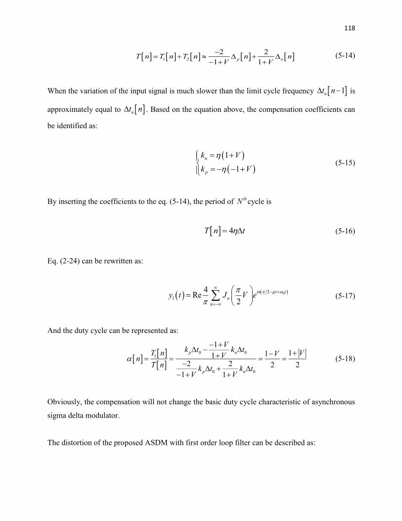
118
1 2
2 2
1 1
p nT n T n T n n n
V V (5-14)
When the variation of the input signal is much slower than the limit cycle frequency 1nt n is
approximately equal to nt n . Based on the equation above, the compensation coefficients can
be identified as:
1
1
n
p
k V
k V
(5-15)
By inserting the coefficients to the eq. (5-14), the period of thN cycle is
4T n t (5-16)
Eq. (2-24) can be rewritten as:
02
1
4Re
2
in t t
n
n
y t J V e
(5-17)
And the duty cycle can be represented as:
0 01
0 0
1111
2 2 2 2
1 1
p n
p n
Vk t k tT n VVVn
T nk t k t
V V
(5-18)
Obviously, the compensation will not change the basic duty cycle characteristic of asynchronous
sigma delta modulator.
The distortion of the proposed ASDM with first order loop filter can be described as:
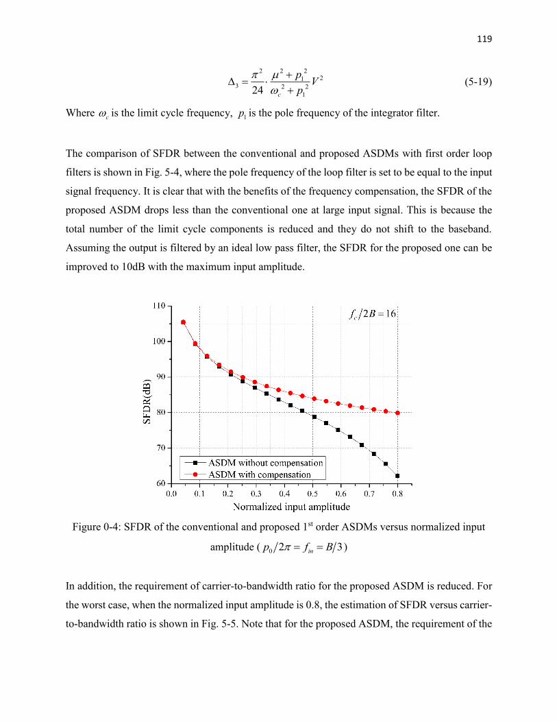
119
2 2221
3 2 2
124 c
pV
p
(5-19)
Where c is the limit cycle frequency, 1p is the pole frequency of the integrator filter.
The comparison of SFDR between the conventional and proposed ASDMs with first order loop
filters is shown in Fig. 5-4, where the pole frequency of the loop filter is set to be equal to the input
signal frequency. It is clear that with the benefits of the frequency compensation, the SFDR of the
proposed ASDM drops less than the conventional one at large input signal. This is because the
total number of the limit cycle components is reduced and they do not shift to the baseband.
Assuming the output is filtered by an ideal low pass filter, the SFDR for the proposed one can be
improved to 10dB with the maximum input amplitude.
Figure 0-4: SFDR of the conventional and proposed 1st order ASDMs versus normalized input
amplitude ( 0 2 3inp f B )
In addition, the requirement of carrier-to-bandwidth ratio for the proposed ASDM is reduced. For
the worst case, when the normalized input amplitude is 0.8, the estimation of SFDR versus carrier-
to-bandwidth ratio is shown in Fig. 5-5. Note that for the proposed ASDM, the requirement of the
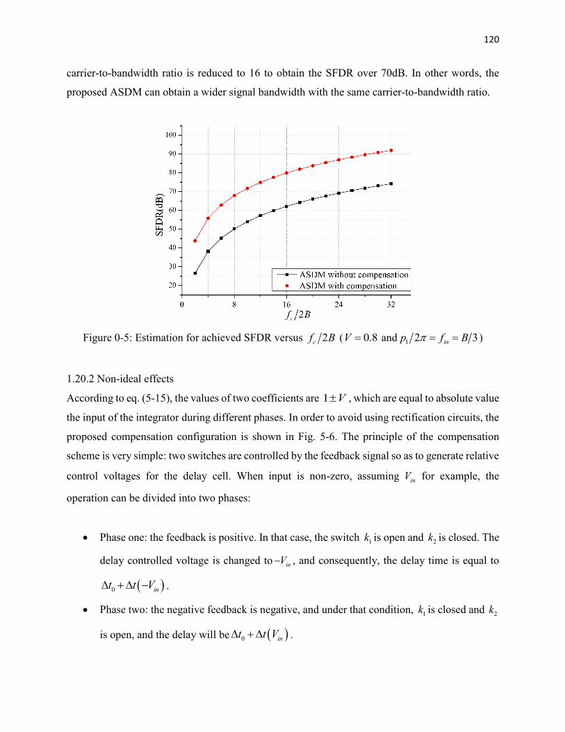
120
carrier-to-bandwidth ratio is reduced to 16 to obtain the SFDR over 70dB. In other words, the
proposed ASDM can obtain a wider signal bandwidth with the same carrier-to-bandwidth ratio.
Figure 0-5: Estimation for achieved SFDR versus 2cf B ( 0.8V and 1 2 3inp f B )
1.20.2 Non-ideal effects
According to eq. (5-15), the values of two coefficients are 1 V , which are equal to absolute value
the input of the integrator during different phases. In order to avoid using rectification circuits, the
proposed compensation configuration is shown in Fig. 5-6. The principle of the compensation
scheme is very simple: two switches are controlled by the feedback signal so as to generate relative
control voltages for the delay cell. When input is non-zero, assuming inV for example, the
operation can be divided into two phases:
Phase one: the feedback is positive. In that case, the switch 1k is open and 2k is closed. The
delay controlled voltage is changed to inV , and consequently, the delay time is equal to
0 int t V .
Phase two: the negative feedback is negative, and under that condition, 1k is closed and 2k
is open, and the delay will be 0 int t V .
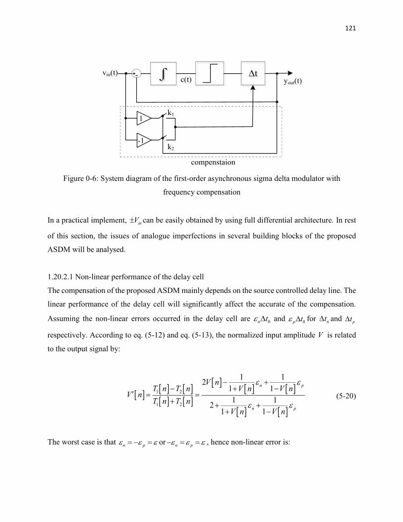
121
ʃʃ ΔtΔtvin(t)yout(t)c(t)
1
-1
compenstaion
k1
k2
Figure 0-6: System diagram of the first-order asynchronous sigma delta modulator with
frequency compensation
In a practical implement, inV can be easily obtained by using full differential architecture. In rest
of this section, the issues of analogue imperfections in several building blocks of the proposed
ASDM will be analysed.
1.20.2.1 Non-linear performance of the delay cell
The compensation of the proposed ASDM mainly depends on the source controlled delay line. The
linear performance of the delay cell will significantly affect the accurate of the compensation.
Assuming the non-linear errors occurred in the delay cell are 0n t and 0p t for nt and
pt
respectively. According to eq. (5-12) and eq. (5-13), the normalized input amplitude V is related
to the output signal by:
1 2
1 2
1 12
1 1
1 12
1 1
n p
n p
V nT n T n V n V n
V nT n T n
V n V n
(5-20)
The worst case is that n p or
n p , hence non-linear error is:
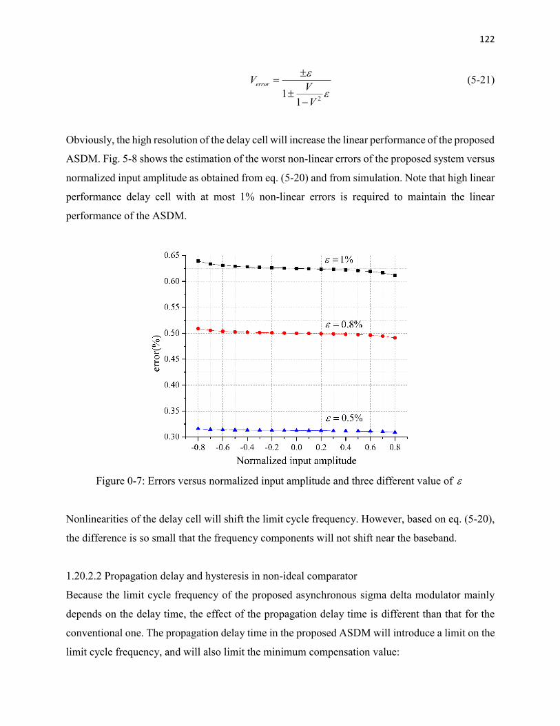
122
21
1
errorVV
V
(5-21)
Obviously, the high resolution of the delay cell will increase the linear performance of the proposed
ASDM. Fig. 5-8 shows the estimation of the worst non-linear errors of the proposed system versus
normalized input amplitude as obtained from eq. (5-20) and from simulation. Note that high linear
performance delay cell with at most 1% non-linear errors is required to maintain the linear
performance of the ASDM.
Figure 0-7: Errors versus normalized input amplitude and three different value of
Nonlinearities of the delay cell will shift the limit cycle frequency. However, based on eq. (5-20),
the difference is so small that the frequency components will not shift near the baseband.
1.20.2.2 Propagation delay and hysteresis in non-ideal comparator
Because the limit cycle frequency of the proposed asynchronous sigma delta modulator mainly
depends on the delay time, the effect of the propagation delay time is different than that for the
conventional one. The propagation delay time in the proposed ASDM will introduce a limit on the
limit cycle frequency, and will also limit the minimum compensation value:
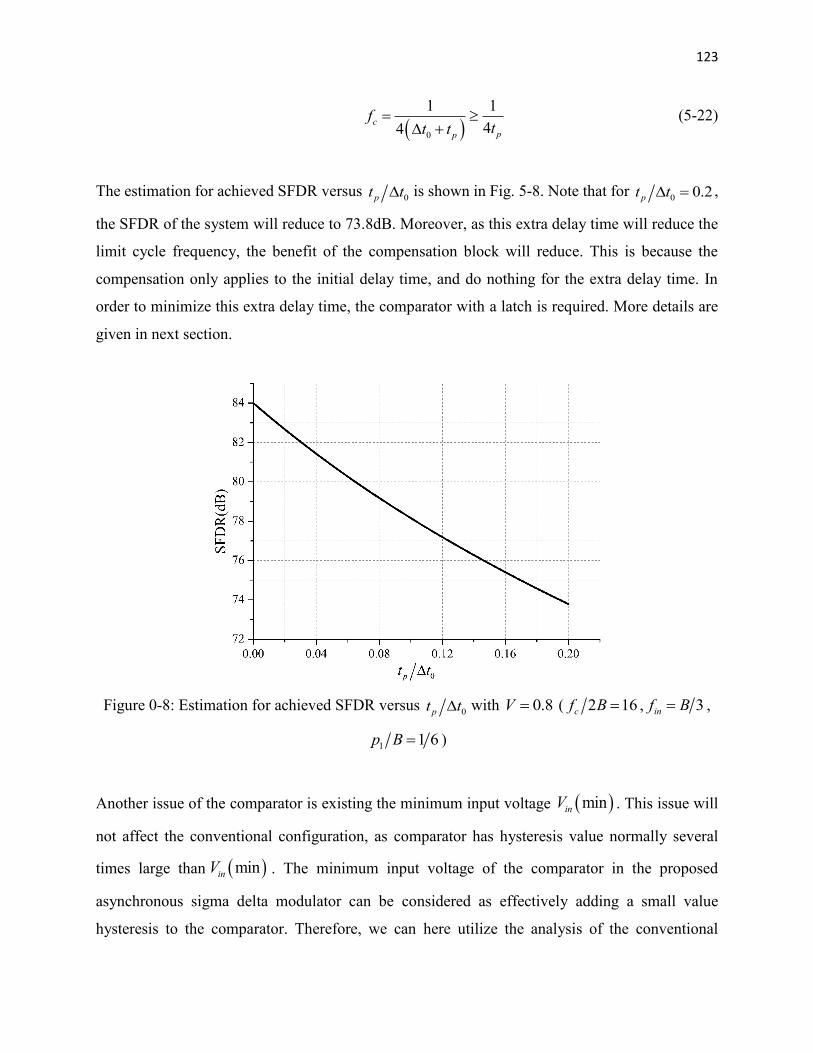
123
0
1 1
44c
pp
ftt t
(5-22)
The estimation for achieved SFDR versus 0pt t is shown in Fig. 5-8. Note that for
0 0.2pt t ,
the SFDR of the system will reduce to 73.8dB. Moreover, as this extra delay time will reduce the
limit cycle frequency, the benefit of the compensation block will reduce. This is because the
compensation only applies to the initial delay time, and do nothing for the extra delay time. In
order to minimize this extra delay time, the comparator with a latch is required. More details are
given in next section.
Figure 0-8: Estimation for achieved SFDR versus 0pt t with 0.8V ( 2 16cf B , 3inf B ,
1 1 6p B )
Another issue of the comparator is existing the minimum input voltage mininV . This issue will
not affect the conventional configuration, as comparator has hysteresis value normally several
times large than mininV . The minimum input voltage of the comparator in the proposed
asynchronous sigma delta modulator can be considered as effectively adding a small value
hysteresis to the comparator. Therefore, we can here utilize the analysis of the conventional
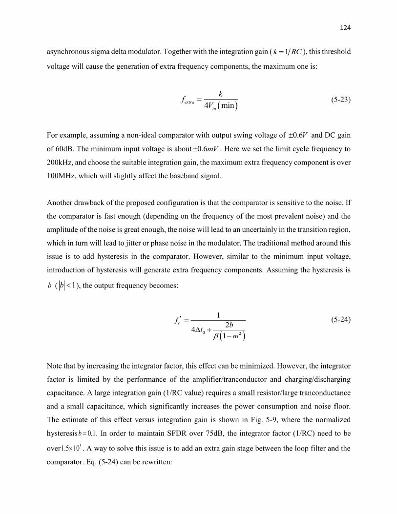
124
asynchronous sigma delta modulator. Together with the integration gain ( 1k RC ), this threshold
voltage will cause the generation of extra frequency components, the maximum one is:
4 minextra
in
kf
V (5-23)
For example, assuming a non-ideal comparator with output swing voltage of 0.6V and DC gain
of 60dB. The minimum input voltage is about 0.6mV . Here we set the limit cycle frequency to
200kHz, and choose the suitable integration gain, the maximum extra frequency component is over
100MHz, which will slightly affect the baseband signal.
Another drawback of the proposed configuration is that the comparator is sensitive to the noise. If
the comparator is fast enough (depending on the frequency of the most prevalent noise) and the
amplitude of the noise is great enough, the noise will lead to an uncertainly in the transition region,
which in turn will lead to jitter or phase noise in the modulator. The traditional method around this
issue is to add hysteresis in the comparator. However, similar to the minimum input voltage,
introduction of hysteresis will generate extra frequency components. Assuming the hysteresis is
b ( 1b ), the output frequency becomes:
0 2
1
24
1
cf bt
m
(5-24)
Note that by increasing the integrator factor, this effect can be minimized. However, the integrator
factor is limited by the performance of the amplifier/tranconductor and charging/discharging
capacitance. A large integration gain (1/RC value) requires a small resistor/large tranconductance
and a small capacitance, which significantly increases the power consumption and noise floor.
The estimate of this effect versus integration gain is shown in Fig. 5-9, where the normalized
hysteresis 0.1b . In order to maintain SFDR over 75dB, the integrator factor (1/RC) need to be
over51.5 10 . A way to solve this issue is to add an extra gain stage between the loop filter and the
comparator. Eq. (5-24) can be rewritten:
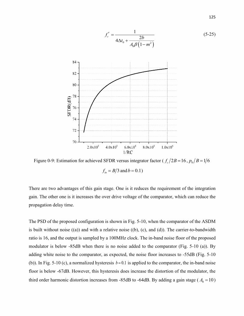
125
0 2
0
1
24
1
cf bt
A m
(5-25)
Figure 0-9: Estimation for achieved SFDR versus integrator factor ( 2 16cf B , 0 1 6p B
3inf B and 0.1b )
There are two advantages of this gain stage. One is it reduces the requirement of the integration
gain. The other one is it increases the over drive voltage of the comparator, which can reduce the
propagation delay time.
The PSD of the proposed configuration is shown in Fig. 5-10, when the comparator of the ASDM
is built without noise ((a)) and with a relative noise ((b), (c), and (d)). The carrier-to-bandwidth
ratio is 16, and the output is sampled by a 100MHz clock. The in-band noise floor of the proposed
modulator is below -85dB when there is no noise added to the comparator (Fig. 5-10 (a)). By
adding white noise to the comparator, as expected, the noise floor increases to -55dB (Fig. 5-10
(b)). In Fig. 5-10 (c), a normalized hysteresis 0.1b is applied to the comparator, the in-band noise
floor is below -67dB. However, this hysteresis does increase the distortion of the modulator, the
third order harmonic distortion increases from -85dB to -64dB. By adding a gain stage ( 0 10A )
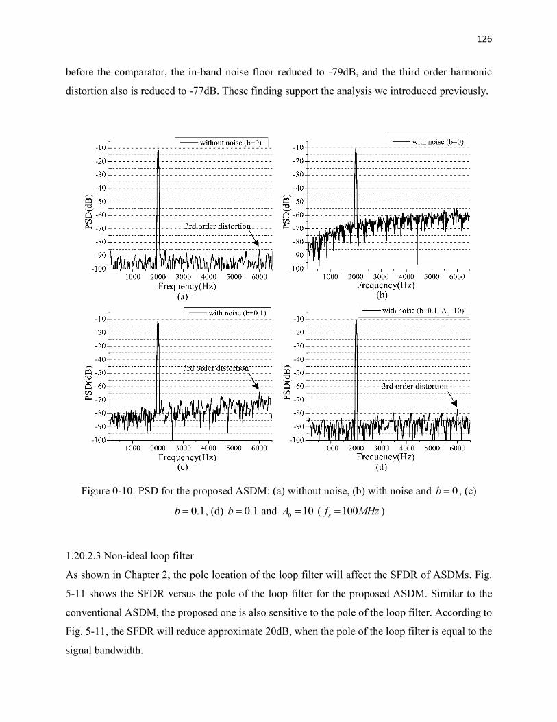
126
before the comparator, the in-band noise floor reduced to -79dB, and the third order harmonic
distortion also is reduced to -77dB. These finding support the analysis we introduced previously.
Figure 0-10: PSD for the proposed ASDM: (a) without noise, (b) with noise and 0b , (c)
0.1b , (d) 0.1b and 0 10A ( 100sf MHz )
1.20.2.3 Non-ideal loop filter
As shown in Chapter 2, the pole location of the loop filter will affect the SFDR of ASDMs. Fig.
5-11 shows the SFDR versus the pole of the loop filter for the proposed ASDM. Similar to the
conventional ASDM, the proposed one is also sensitive to the pole of the loop filter. According to
Fig. 5-11, the SFDR will reduce approximate 20dB, when the pole of the loop filter is equal to the
signal bandwidth.
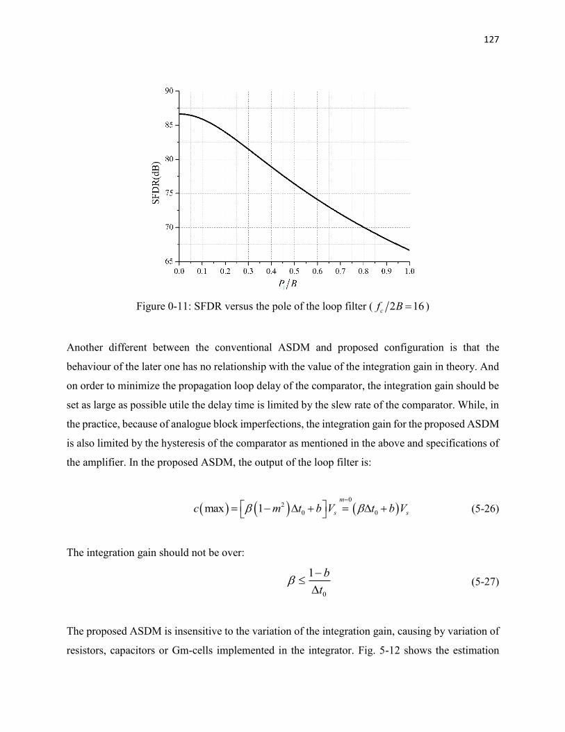
127
Figure 0-11: SFDR versus the pole of the loop filter ( 2 16cf B )
Another different between the conventional ASDM and proposed configuration is that the
behaviour of the later one has no relationship with the value of the integration gain in theory. And
on order to minimize the propagation loop delay of the comparator, the integration gain should be
set as large as possible utile the delay time is limited by the slew rate of the comparator. While, in
the practice, because of analogue block imperfections, the integration gain for the proposed ASDM
is also limited by the hysteresis of the comparator as mentioned in the above and specifications of
the amplifier. In the proposed ASDM, the output of the loop filter is:
0
2
0 0max 1m
s sc m t b V t b V
(5-26)
The integration gain should not be over:
0
1 b
t
(5-27)
The proposed ASDM is insensitive to the variation of the integration gain, causing by variation of
resistors, capacitors or Gm-cells implemented in the integrator. Fig. 5-12 shows the estimation
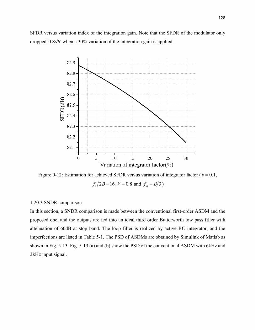
128
SFDR versus variation index of the integration gain. Note that the SFDR of the modulator only
dropped 0.8dB when a 30% variation of the integration gain is applied.
Figure 0-12: Estimation for achieved SFDR versus variation of integrator factor ( 0.1b ,
2 16cf B , 0.8V and 3inf B )
1.20.3 SNDR comparison
In this section, a SNDR comparison is made between the conventional first-order ASDM and the
proposed one, and the outputs are fed into an ideal third order Butterworth low pass filter with
attenuation of 60dB at stop band. The loop filter is realized by active RC integrator, and the
imperfections are listed in Table 5-1. The PSD of ASDMs are obtained by Simulink of Matlab as
shown in Fig. 5-13. Fig. 5-13 (a) and (b) show the PSD of the conventional ASDM with 6kHz and
3kHz input signal.
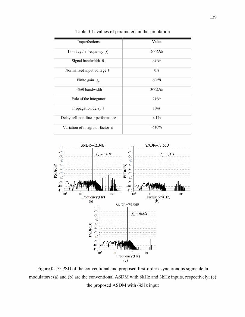
129
Table 0-1: values of parameters in the simulation
Imperfections Value
Limit cycle frequency cf 200kHz
Signal bandwidth B 6kHz
Normalized input voltage V 0.8
Finite gain 0A 60dB
3dB bandwidth 300kHz
Pole of the integrator 2kHz
Propagation delay t 10ns
Delay cell non-linear performance 1%
Variation of integrator factor k 10%
Figure 0-13: PSD of the conventional and proposed first-order asynchronous sigma delta
modulators: (a) and (b) are the conventional ASDM with 6kHz and 3kHz inputs, respectively; (c)
the proposed ASDM with 6kHz input
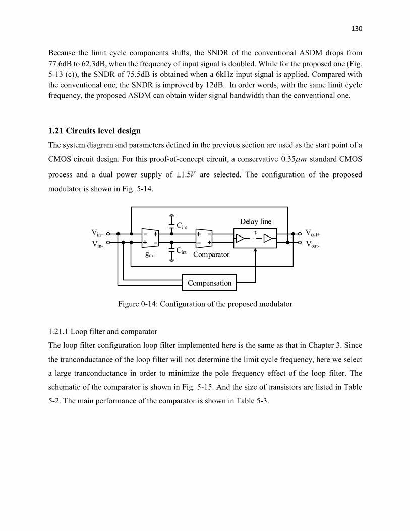
130
Because the limit cycle components shifts, the SNDR of the conventional ASDM drops from
77.6dB to 62.3dB, when the frequency of input signal is doubled. While for the proposed one (Fig.
5-13 (c)), the SNDR of 75.5dB is obtained when a 6kHz input signal is applied. Compared with
the conventional one, the SNDR is improved by 12dB. In order words, with the same limit cycle
frequency, the proposed ASDM can obtain wider signal bandwidth than the conventional one.
1.21 Circuits level design
The system diagram and parameters defined in the previous section are used as the start point of a
CMOS circuit design. For this proof-of-concept circuit, a conservative 0.35 m standard CMOS
process and a dual power supply of 1.5V are selected. The configuration of the proposed
modulator is shown in Fig. 5-14.
gm1Cint
Vout+Vin+
Cint
Vout-Vin-
Comparator
τ
Delay line
Compensation
Figure 0-14: Configuration of the proposed modulator
1.21.1 Loop filter and comparator
The loop filter configuration loop filter implemented here is the same as that in Chapter 3. Since
the tranconductance of the loop filter will not determine the limit cycle frequency, here we select
a large tranconductance in order to minimize the pole frequency effect of the loop filter. The
schematic of the comparator is shown in Fig. 5-15. And the size of transistors are listed in Table
5-2. The main performance of the comparator is shown in Table 5-3.
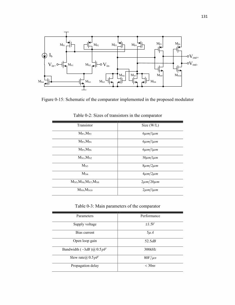
131
MN1
Ib
Vin+ Vin-
Vout+
Vout-MN2
MN3MN4 MN5
MN6 MN7 MN9
MN8
MN10
MP1 MP2 MP3 MP4MP5 MP6
Figure 0-15: Schematic of the comparator implemented in the proposed modulator
Table 0-2: Sizes of transistors in the comparator
Transistor Size (W/L)
MP1,MP2 6 1m m
MP3,MP4 6 1m m
MP5,MP6 6 1m m
MN1,MN2 50 1m m
MN3 8 2m m
MN4 4 2m m
MN5,MN6,MN7,MN8 2 20m m
MN9,MN10 2 1m m
Table 0-3: Main parameters of the comparator
Parameters Performance
Supply voltage 1.5V
Bias current 5 A
Open loop gain 52.5dB
Bandwidth ( 3dB )@ 0.5pF 300kHz
Slew rate@ 0.5pF 80V s
Propagation delay 30ns
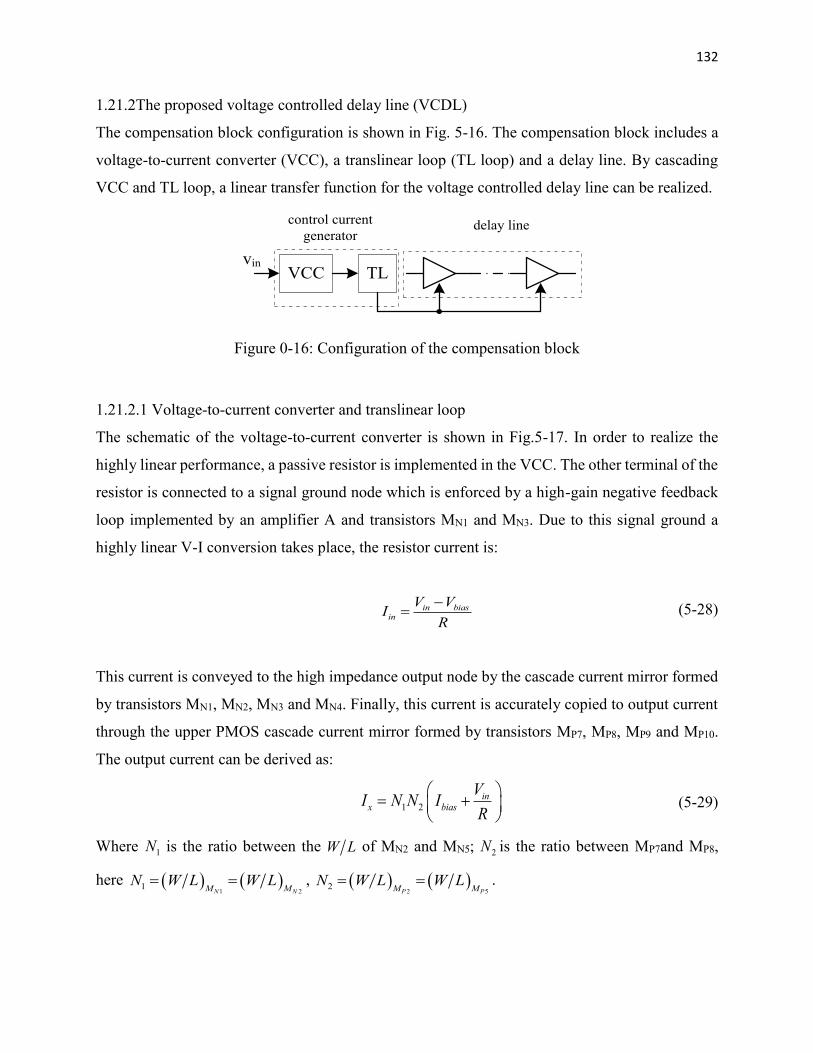
132
1.21.2The proposed voltage controlled delay line (VCDL)
The compensation block configuration is shown in Fig. 5-16. The compensation block includes a
voltage-to-current converter (VCC), a translinear loop (TL loop) and a delay line. By cascading
VCC and TL loop, a linear transfer function for the voltage controlled delay line can be realized.
delay line
VCC TLvin
control current
generator
Figure 0-16: Configuration of the compensation block
1.21.2.1 Voltage-to-current converter and translinear loop
The schematic of the voltage-to-current converter is shown in Fig.5-17. In order to realize the
highly linear performance, a passive resistor is implemented in the VCC. The other terminal of the
resistor is connected to a signal ground node which is enforced by a high-gain negative feedback
loop implemented by an amplifier A and transistors MN1 and MN3. Due to this signal ground a
highly linear V-I conversion takes place, the resistor current is:
in biasin
V VI
R
(5-28)
This current is conveyed to the high impedance output node by the cascade current mirror formed
by transistors MN1, MN2, MN3 and MN4. Finally, this current is accurately copied to output current
through the upper PMOS cascade current mirror formed by transistors MP7, MP8, MP9 and MP10.
The output current can be derived as:
1 2in
x bias
VI N N I
R
(5-29)
Where 1N is the ratio between the W L of MN2 and MN5; 2N is the ratio between MP7and MP8,
here 1 2
1N NM M
N W L W L , 2 5
2P PM M
N W L W L .
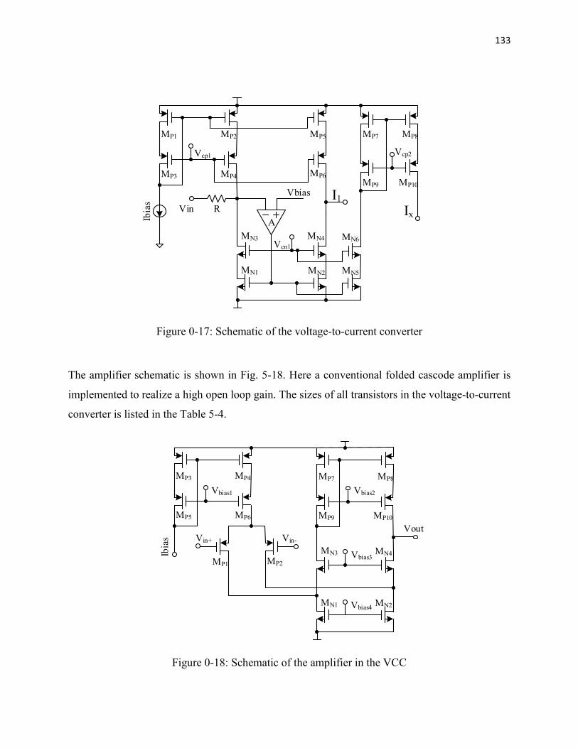
133
Ibia
s
Vbias
IxVin R
Vcp2Vcp1
MN1 MN2
MN3 MN4
A
MP1 MP2
MP3 MP4
MP5
I1
MP7 MP8
Vcn1
MP9 MP10
MN5
MN6
MP6
Figure 0-17: Schematic of the voltage-to-current converter
The amplifier schematic is shown in Fig. 5-18. Here a conventional folded cascode amplifier is
implemented to realize a high open loop gain. The sizes of all transistors in the voltage-to-current
converter is listed in the Table 5-4.
Vbias2
MP7 MP8
MP9 MP10
MN2
MN4
MN1
MN3
MP2MP1
Vbias1
MP3 MP4
MP5 MP6
Ibia
s Vin+ Vin-
Vbias3
Vbias4
Vout
Figure 0-18: Schematic of the amplifier in the VCC
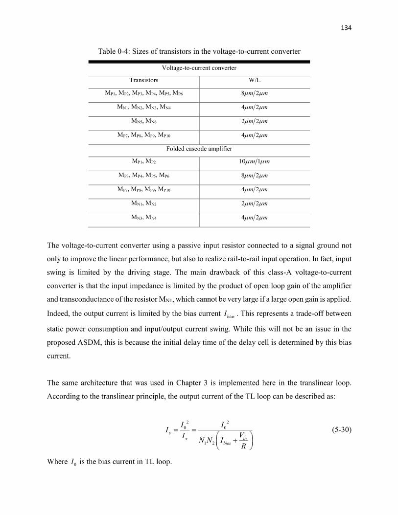
134
Table 0-4: Sizes of transistors in the voltage-to-current converter
Voltage-to-current converter
Transistors W/L
MP1, MP2, MP3, MP4, MP5, MP6 8 2m m
MN1, MN2, MN3, MN4 4 2m m
MN5, MN6 2 2m m
MP7, MP8, MP9, MP10 4 2m m
Folded cascode amplifier
MP1, MP2 10 1m m
MP3, MP4, MP5, MP6 8 2m m
MP7, MP8, MP9, MP10 4 2m m
MN1, MN2 2 2m m
MN3, MN4 4 2m m
The voltage-to-current converter using a passive input resistor connected to a signal ground not
only to improve the linear performance, but also to realize rail-to-rail input operation. In fact, input
swing is limited by the driving stage. The main drawback of this class-A voltage-to-current
converter is that the input impedance is limited by the product of open loop gain of the amplifier
and transconductance of the resistor MN1, which cannot be very large if a large open gain is applied.
Indeed, the output current is limited by the bias current biasI . This represents a trade-off between
static power consumption and input/output current swing. While this will not be an issue in the
proposed ASDM, this is because the initial delay time of the delay cell is determined by this bias
current.
The same architecture that was used in Chapter 3 is implemented here in the translinear loop.
According to the translinear principle, the output current of the TL loop can be described as:
2 2
0 0
1 2
y
inxbias
I II
VIN N I
R
(5-30)
Where 0I is the bias current in TL loop.
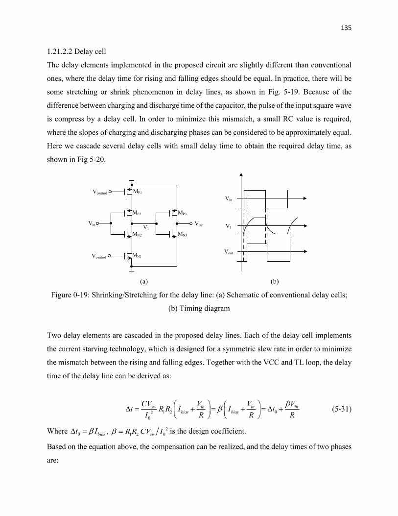
135
1.21.2.2 Delay cell
The delay elements implemented in the proposed circuit are slightly different than conventional
ones, where the delay time for rising and falling edges should be equal. In practice, there will be
some stretching or shrink phenomenon in delay lines, as shown in Fig. 5-19. Because of the
difference between charging and discharge time of the capacitor, the pulse of the input square wave
is compress by a delay cell. In order to minimize this mismatch, a small RC value is required,
where the slopes of charging and discharging phases can be considered to be approximately equal.
Here we cascade several delay cells with small delay time to obtain the required delay time, as
shown in Fig 5-20.
Vin
Vout
V1
MP1
MP2 MP3
MN3MN2
MN1Vcontrol
Vcontrol
Vin VoutV1
(a) (b)
Figure 0-19: Shrinking/Stretching for the delay line: (a) Schematic of conventional delay cells;
(b) Timing diagram
Two delay elements are cascaded in the proposed delay lines. Each of the delay cell implements
the current starving technology, which is designed for a symmetric slew rate in order to minimize
the mismatch between the rising and falling edges. Together with the VCC and TL loop, the delay
time of the delay line can be derived as:
1 2 02
0
sw in in inbias bias
CV V V Vt R R I I t
I R R R
(5-31)
Where 0 biast I , 2
1 2 0swR R CV I is the design coefficient.
Based on the equation above, the compensation can be realized, and the delay times of two phases
are:
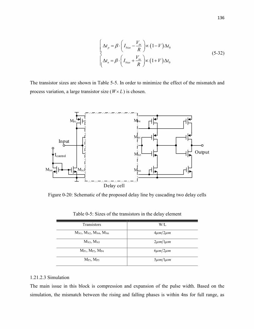
136
0
0
1
1
inp bias
inn bias
Vt I V t
R
Vt I V t
R
(5-32)
The transistor sizes are shown in Table 5-5. In order to minimize the effect of the mismatch and
process variation, a large transistor size (W L ) is chosen.
MP1
Icontrol
MP2
MP3
MN3
MN2MN1MN4
Input
Output
Delay cell
MP4
MP5
MN5
MN6
Figure 0-20: Schematic of the proposed delay line by cascading two delay cells
Table 0-5: Sizes of the transistors in the delay element
Transistors W/L
MN1, MN2, MN4, MN6 4 2m m
MN3, MN5 2 1m m
MP1, MP2, MP4 6 2m m
MP3, MP5 5 1m m
1.21.2.3 Simulation
The main issue in this block is compression and expansion of the pulse width. Based on the
simulation, the mismatch between the rising and falling phases is within 4ns for full range, as
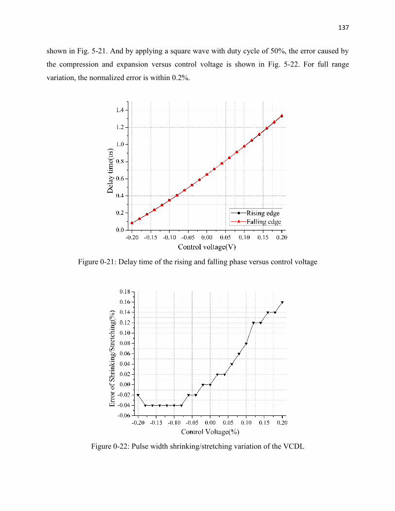
137
shown in Fig. 5-21. And by applying a square wave with duty cycle of 50%, the error caused by
the compression and expansion versus control voltage is shown in Fig. 5-22. For full range
variation, the normalized error is within 0.2%.
Figure 0-21: Delay time of the rising and falling phase versus control voltage
Figure 0-22: Pulse width shrinking/stretching variation of the VCDL
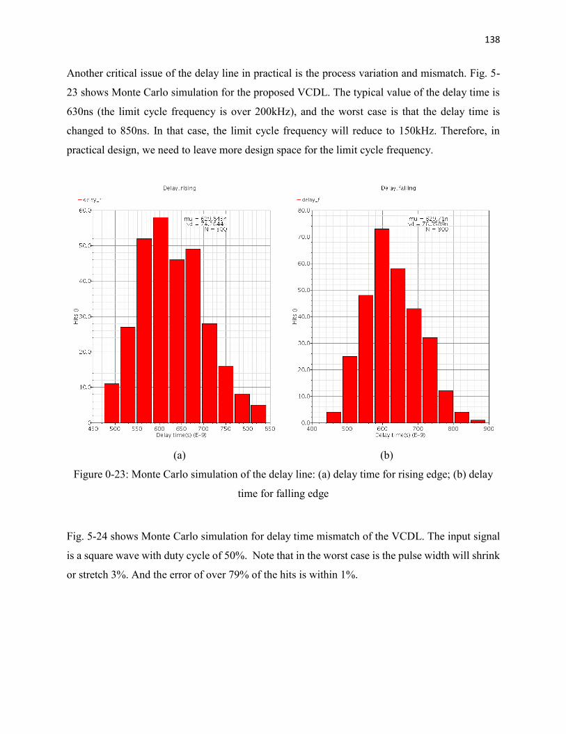
138
Another critical issue of the delay line in practical is the process variation and mismatch. Fig. 5-
23 shows Monte Carlo simulation for the proposed VCDL. The typical value of the delay time is
630ns (the limit cycle frequency is over 200kHz), and the worst case is that the delay time is
changed to 850ns. In that case, the limit cycle frequency will reduce to 150kHz. Therefore, in
practical design, we need to leave more design space for the limit cycle frequency.
(a) (b)
Figure 0-23: Monte Carlo simulation of the delay line: (a) delay time for rising edge; (b) delay
time for falling edge
Fig. 5-24 shows Monte Carlo simulation for delay time mismatch of the VCDL. The input signal
is a square wave with duty cycle of 50%. Note that in the worst case is the pulse width will shrink
or stretch 3%. And the error of over 79% of the hits is within 1%.
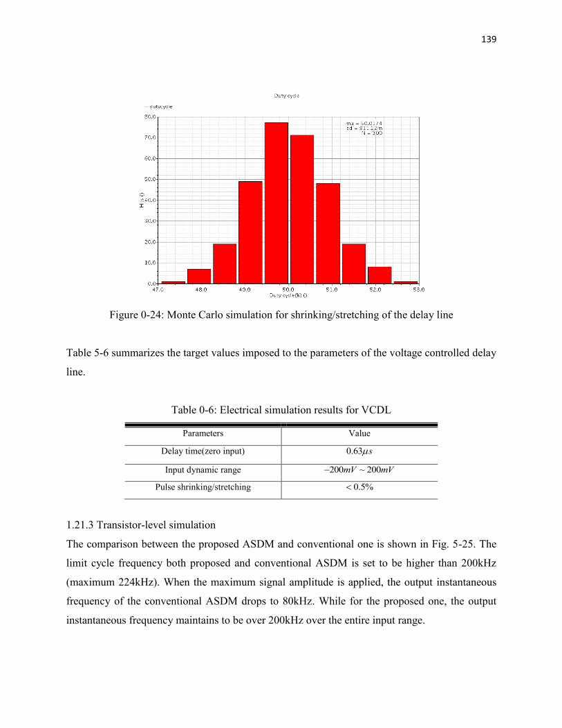
139
Figure 0-24: Monte Carlo simulation for shrinking/stretching of the delay line
Table 5-6 summarizes the target values imposed to the parameters of the voltage controlled delay
line.
Table 0-6: Electrical simulation results for VCDL
Parameters Value
Delay time(zero input) 0.63 s
Input dynamic range 200 ~ 200mV mV
Pulse shrinking/stretching 0.5%
1.21.3 Transistor-level simulation
The comparison between the proposed ASDM and conventional one is shown in Fig. 5-25. The
limit cycle frequency both proposed and conventional ASDM is set to be higher than 200kHz
(maximum 224kHz). When the maximum signal amplitude is applied, the output instantaneous
frequency of the conventional ASDM drops to 80kHz. While for the proposed one, the output
instantaneous frequency maintains to be over 200kHz over the entire input range.
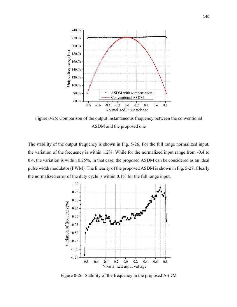
140
Figure 0-25: Comparison of the output instantaneous frequency between the conventional
ASDM and the proposed one
The stability of the output frequency is shown in Fig. 5-26. For the full range normalized input,
the variation of the frequency is within 1.2%. While for the normalized input range from -0.4 to
0.4, the variation is within 0.25%. In that case, the proposed ASDM can be considered as an ideal
pulse width modulator (PWM). The linearity of the proposed ASDM is shown in Fig. 5-27. Clearly
the normalized error of the duty cycle is within 0.1% for the full range input.
Figure 0-26: Stability of the frequency in the proposed ASDM
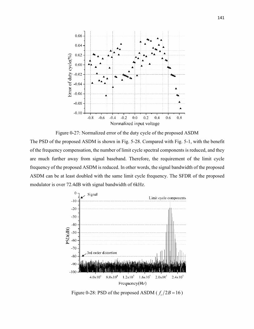
141
Figure 0-27: Normalized error of the duty cycle of the proposed ASDM
The PSD of the proposed ASDM is shown in Fig. 5-28. Compared with Fig. 5-1, with the benefit
of the frequency compensation, the number of limit cycle spectral components is reduced, and they
are much further away from signal baseband. Therefore, the requirement of the limit cycle
frequency of the proposed ASDM is reduced. In other words, the signal bandwidth of the proposed
ASDM can be at least doubled with the same limit cycle frequency. The SFDR of the proposed
modulator is over 72.4dB with signal bandwidth of 6kHz.
Figure 0-28: PSD of the proposed ASDM ( 2 16cf B )
142
1.22 Summary
In this chapter, a novel asynchronous sigma delta modulator with frequency compensation is
presented. The proposed ASDM implements a source controlled delay cell instead of the hysteresis
in the comparator to control the limit cycle frequency. The purpose of this proposed modulator is
to apply compensation so as to stabilize the instantaneous output frequency. The compensation
block is realized by an improved voltage controlled delay cell, which comprises a voltage-to-
current converter, a translinear loop and a current starving delay cell. The selecting path chooses
the suitable control voltage in different phases, and feeds it to the voltage-to-current converter to
generate a compensation current. A current mode translinear loop is used to generate a control
current for the delay cell in order to achieve linear delay control.
The proposed asynchronous sigma delta modulator achieves a higher accuracy than the
conventional one in the signal band, as demonstrated by theoretical analysis. This is also
demonstrated by simulation. According to Cadence Spectre transistor-level simulation, the
variation of the output frequency is within 1.2% for full range input ( 0.8V ), and the non-linear
error is within 0.1%. The proposed ASDM can realize a significantly wider signal bandwidth with
the same limit cycle frequency than the conventional ASDM. According to the simulation results,
the signal bandwidth of the proposed ASDM is 6kHz with SFDR over 72.4dB.
143
Conclusions
1.23 Conclusion
This work studied a new type of sigma delta modulators, known as the asynchronous sigma delta
modulator, where the sampled quantiser is replaced by a continuous-time comparator with
hysteresis. As the main advantages of using an asynchronous sigma delta modulator instead of the
synchronous continuous-time sigma delta modulator we highlight the following:
Much simpler configuration. For the conventional synchronous continuous-time sigma
delta modulators, at least a second or high order loop filter is required to obtain a high
resolution. Additionally, in order to improve stability, a multi-bit quantiser is normally
implemented, which requires an equivalent multi-bit DAC in the feedback loop. In
asynchronous sigma delta modulators, a first order loop filter is enough to achieve a high
resolution. As signal information is converted into time signal, the two-level comparator
does not cause the instability problem.
Absence of a sampling clock. Because of the absence of the clock speed constraint,
asynchronous sigma delta modulators can, in theory, achieve an ultra-wide bandwidth.
Clock jitter immunity. As there is no sampling process and DAC in the loop, asynchronous
sigma delta modulators are immune to the clock jitter.
Low power consumption.
On the other hand, asynchronous sigma delta modulators also have several issues, which influence
the circuit design and applications. These are:
144
Limit cycle components, which reduce the effective signal bandwidth and require a high
order filter.
Lack of noise shaping, so that a high resolution decoding circuit is required to maintain the
performance of the modulator.
Distortion due to:
Finite limit cycle frequency
Propagation loop delay
The main contributions of the thesis are:
1. Systematic analyse the non-ideal performance of asynchronous sigma delta modulators,
including the non-deal integrator, propagation loop delay.
2. Introduction of a new effective decoding solution for asynchronous sigma delta modulators.
The decoding circuit implements a special coarse-fine time-to-digital converter to quantise
the square wave produced by asynchronous sigma delta modulators, and converts the duty
cycle to a digital output. The time-to-digital converter operates asynchronously by utilizing
vernier delay lines. The purpose of this circuit is to achieve a high resolution with a low
frequency sampling clock, which is suitable for the ultra-low power applications. The
proposed circuit is designed in AMS 0.35 m CMOS process. Spectre simulations, show
that an 11-bit resolution can be realized.
3. Proposed a novel architecture of asynchronous sigma delta modulators with noise shaping.
The proposed modulator introduces an 8-phase sampler after the comparator as the
quantiser. A single-bit digital-to-time converter rather than the conventional multi-bit DAC
is implemented to reconstruct a feedback signal. According to Spectre/Cadence
simulations the proposed modulator with noise shaping can achieved peak SNDR of
78.2dB, which is 22dB better than the conventional asynchronous sigma delta modulator
which uses same sampler.
145
4. Developed a compensation methodology to realize an improved asynchronous sigma delta
modulator with constant limit cycle frequency. The purpose of the frequency compensation
is to make the instantaneous output frequency constant so as to minimize the effect of the
limit cycle frequency components when a large signal is applied. The compensation circuit
is realized by a special voltage controlled delay line, which the delay time is related to the
input signal. The proposed ASDM is designed to have a 6kHz signal bandwidth with the
carrier-to-bandwidth ratio ( 2cf B ) of 16. Spectre/Cadence simulation demonstrate a non-
linear error is less than 0.1% with full range input from -200mV to 200mV. The variation
of the output frequency is within 1.2% for full range input. The SFDR of the proposed
ASDM is over 72.4dB.
The first chip of asynchronous sigma delta modulators was fabricated by Philips 8 years ago. The
test results did show some attractive properties, such as better resolution than flash ADCs and
lower power dissipation than CT-SDMs [49]. However, the development of ASDMs is not
remarkable. This is because it requires a high frequency sampling clock to digitise the output signal,
especially for bluetooth and WIFI applications. Unfortunately, this is limited by the current CMOS
process. Now, with solutions of the decoding scheme and noise shaping shown in this thesis,
ASDMs have opportunities to implement in these applications in a modern CMOS process.
Moreover, the ASDM can also be applied on biomedical applications, where the SAR ADC is the
only option in this application right now. Currently, many researchers focus on using CT-SDMs
in this application. However, there is still a long way to go for CT-SDMs because of their high
power dissipation. Similar to the high frequency applications, I believe that ASDMs can also
obtain a low power dissipation in ultra-low power applications. With the benefit of frequency
compensation, the power dissipation in digital decimation can also be reduced. In the feature,
ASDMs will become good choice to fill the gap between SAR ADCs and CT-SDMs, and the gap
between flash ADCs and CT-SDMs as well.
1.24 Future work
For future investigation and future work the following aspects of the research are suggested:
146
1. The decoding methodology introduced in Chapter 3 can be implemented in high frequency
applicants, and can be realized by FPGAs.
2. As very a few asynchronous sigma delta modulators are fabricated, the novel architectures
introduced in Chapter 4 and Chapter 5 need to be verified on silicon.
3. The power dissipation advantage of ASDMs in biomedical applications is not verified on
silicon. The architecture of ASDMs in Chapter 5 is suitable for low frequency applications.
So in the feature, I will design a specific modulator for biomedical sensors, such as neural
sensors and EGG.
4. Asynchronous sigma delta modulators can also be decoded through frequency
measurement, which uses a highly accurate low frequency, such as a quartz clock, as a
reference.
147
Appendix
Appendix I
1. DC analysis
The Fourier transfer of eq. (2-13) is:
0
1
sin2 2 1 8Re
n
nC V F n F
n
(I-1)
Where 0
0
1 1
sin sincos Re
jn t
n n
n nn t e
n n
; 2 1 2 2 1FT V V ;
0
0
1 1
sin sinRe 2
jn t
n n
n nF e n
n n
; FT f t F ;
Therefore the inverse Fourier transform is:
0
1
4 sin2 1 Rej t j t
n
nc t V F e d n F e d
n
(I-2)
0 0 0 0
1 1
2 1 2 1 0
sin sincos sin
j t
j t
n n
V F e d V F
n nn F e d F n n t j n t
n n
(I-3)
After by incorporation eq. (I-3) into eq. (I-2), eq. (2-16) is obtained.
2. Sine wave signal input
Again, the Fourier transfer of eq. (2-14) is:
148
0
1
sin2 cos 2 1 8Rem m
n
nC V T F n F
n
(I-4)
The inverse Fourier transfer is:
0
1
sincos 2 1 8Rej t
m m
n
nc t V T F e n F
n
(I-5)
By keeping only the real part, eq. (I-5) can be rewritten as:
0 0 0 0
1
cos 2 1 Re cos Im sin
4 sinRe cos Im sin
m m m s m
n
c t V T F T F T
nF n n t F n n t
n
(I-6)
After inserting the boundary conditions the following two equation are obtained:
0 0
1
cos 2 1 Re cos Im sin
4 sinRe cos Im sin
m
n
b V T F t F t
nF n n F n n
n
(I-7)
0 0
1
cos 2 1 Re cos Im sin
4 sinRe cos Im sin
m
n
b V T F t F t
nF n n F n n
n
(I-8)
Where
1 10 1 2 0 1 2cos cos cos cos
2 2
T Tn k T T n k T T n n
and
1 10 1 2 0 1 2sin sin sin
2 2
T Tn k T T n k T T n
149
By addition and subtraction eq. (I-7) and eq. (I-8):
0
1
0
1
4 sincos 2 1 Re cos Re cos
sincos 2 1 Im sin Im sin
4
m
n
m
n
nV T F t F n n
n
n bV T F t F n n
n
(I-9)
11 2
0 0
2
2
Tk T T k
(I-10)
If 0 , we obtain the following approximate result:
0 0 0
22 0k k
(I-11)
From this, eq. (2-20) is easily obtained.
2 2 2 2cos 21 1 sin 2
2 2 4
V V t V Vdt t t
(I-12)
Eq. (2-21) can be rewritten as:
22
cos2
1
4Re Reexp 1 sin 2
2 4
Vi t
cc
VVy t e i t t
(I-13)
Here we implement the Jacobi-Anger expansion, which states that:
exp sin in
n
n
iz J z e
(I-14)
Eq. (2-22) follows.
150
3. Distortion
The Taylor series for a sin x is:
3 5 7
sin3! 5! 7!
x x xx x (I-15)
3
1,3,5
11 sin
6
n
in in in
n
v v v
[87] (I-16)
By inserting cosinv V t , eq. (2-23) can be easily obtained.
151
Appendix II
The Fourier transfer of c t with the propagation loop delay can be written as:
0 0
1
2 cos 2 1
sin8Re cos
s s
n
C V t F
nn n F
n
(II-1)
Hence, c t can be obtained:
1
0 0 0 0 0
0 0 0 0 0
4 sincos 2 1 Re
Re cos cos sin sin
Im sin cos cos sin
s s
n
nc t V t F
n
F n n t n n t n
F n n t n n t n
(II-2)
Because of the overshoot, the boundary conditions for the system with propagation delay can be
expressed as:
11 1 1 1 1 2
12 2 2 2 1 2
1, ,2
1, ,2
Ty t c t b t k T T
Ty t c t b t k T T
(II-3)
Where 1 1 sin m
Vb b k T
; 2 1 sin m
Vb b k T
; 1k RC is the integrator
factor of the loop filter
Inserting eq. (II-3) into eq. (II-2) will result:
1
0 0 0
0 0 0
4 sin1 sin cos 2 1 Re
Re cos cos sin sin
Im sin cos cos sin
m m
n
V nb k T V T F
n
F n n n n n
F n n n n n
(II-4)
152
1
0 0 0
0 0 0
4 sin1 sin cos 2 1 Re
Re cos cos sin sin
Im sin cos cos sin
m m
n
V nb k T V T F
n
F n n n n n
F n n n n n
(II-5)
The limit cycle frequency can be rewritten as:
04
c
bkf A (II-6)
Where 0A is the open loop gain.
After addition and subtraction eq. (II-4) and eq. (II-5), eq. (2-37) can be obtained.
153
Reference
[1] S. R. Norsworthy, R. Schreier, G. C. Temes, and IEEE Circuit & Systems Society. (1996). Delta-Sigma data
converters theory, design, and simulation.
[2] M. W. Hauser and R. W. Brodersen, "Monolithic decimation filtering for custom delta-sigma A/D
converters," in Acoustics, Speech, and Signal Processing, 1988. ICASSP-88., 1988 International Conference
on, 1988, pp. 2005-2008 vol.4.
[3] H. Inose, Y. Yasuda, and J. Murakami, "A Telemetering System by Code Modulation Δ- ΣModulation,"
Space Electronics and Telemetry, IRE Transactions on, vol. SET-8, pp. 204-209, 1962.
[4] V. F. Dias, G. Palmisano, and F. Maloberti, "Noise in mixed continuous-time switched-capacitor sigma-delta
modulators," Circuits, Devices and Systems, IEE Proceedings G, vol. 139, pp. 680-684, 1992.
[5] M. Ortmanns, F. Gerfers, and Y. Manoli, "A continuous-time ΔΣ Modulator with reduced sensitivity to clock
jitter through SCR feedback," Circuits and Systems I: Regular Papers, IEEE Transactions on, vol. 52, pp.
875-884, 2005.
[6] J. A. Cherry and W. M. Snelgrove, "Clock jitter and quantizer metastability in continuous-time delta-sigma
modulators," Circuits and Systems II: Analog and Digital Signal Processing, IEEE Transactions on, vol. 46,
pp. 661-676, 1999.
[7] O. Oliaei and H. Aboushady, "Jitter effects in continuous-time ΣΔ modulators with delayed
return-to-zero feedback," in Electronics, Circuits and Systems, 1998 IEEE International Conference on, 1998,
pp. 351-354 vol.1.
[8] K. Reddy and S. Pavan, "Fundamental limitations of continuous-time delta-sigma modulators due to clock
jitter," in Circuits and Systems, 2006. ISCAS 2006. Proceedings. 2006 IEEE International Symposium on,
2006, pp. 4 pp.-2024.
[9] Y. Aiba, K. Tomioka, Y. Nakashima, K. Hamashita, and S. Bang-Sup, "A Fifth-Order Gm-C Continuous-
Time Delta-Sigma Modulator With Process-Insensitive Input Linear Range," Solid-State Circuits, IEEE
Journal of, vol. 44, pp. 2381-2391, 2009.
[10] J. Jun-Gi, N. Jinho, and Y. Changsik, "A 20-MHz Bandwidth Continuous-Time Sigma-Delta Modulator With
Jitter Immunity Improved Full Clock Period SCR (FSCR) DAC and High-Speed DWA," Solid-State Circuits,
IEEE Journal of, vol. 46, pp. 2469-2477, 2011.
[11] M. Keller, A. Buhmann, J. Sauerbrey, M. Ortmanns, and Y. Manoli, "A Comparative Study on Excess-Loop-
Delay Compensation Techniques for Continuous-Time Sigma-Delta Modulators," Circuits and Systems I:
Regular Papers, IEEE Transactions on, vol. 55, pp. 3480-3487, 2008.
[12] S. Pavan, "Excess Loop Delay Compensation in Continuous-Time Delta-Sigma Modulators," Circuits and
Systems II: Express Briefs, IEEE Transactions on, vol. 55, pp. 1119-1123, 2008.
[13] C. Youngcheol, L. Inhee, and H. Gunhee, "A 0.7V 36μW 85dB-DR Audio ΔΣ Modulator Using Class-C
Inverter," in Solid-State Circuits Conference, 2008. ISSCC 2008. Digest of Technical Papers. IEEE
International, 2008, pp. 490-630.
[14] R. H. M. Van Veldhoven, R. Rutten, and L. J. Breems, "An Inverter-Based Hybrid ΔΣ Modulator," in Solid-
State Circuits Conference, 2008. ISSCC 2008. Digest of Technical Papers. IEEE International, 2008, pp.
492-630.
[15] K. Lee, C. Jeongseok, M. Aniya, K. Hamashita, K. Takasuka, S. Takeuchi, et al., "A Noise-Coupled Time-
Interleaved ΔΣ ADC with 4.2MHz BW, -98dB THD, and 79dB SNDR," in Solid-State Circuits Conference,
2008. ISSCC 2008. Digest of Technical Papers. IEEE International, 2008, pp. 494-631.
[16] P. Malla, H. Lakdawala, K. Kornegay, and K. Soumyanath, "A 28mW Spectrum-Sensing Reconfigurable
20MHz 72dB-SNR 70dB-SNDR DT ΔΣ ADC for 802.11n/WiMAX Receivers," in Solid-State Circuits
Conference, 2008. ISSCC 2008. Digest of Technical Papers. IEEE International, 2008, pp. 496-631.
[17] P. Hyunsik, N. KiYoung, D. K. Su, K. Vleugels, and B. A. Wooley, "A 0.7-V 100-dB 870-μW digital audio
ΣΔ modulator," in VLSI Circuits, 2008 IEEE Symposium on, 2008, pp. 178-179.
[18] L. Bos, G. Vandersteen, J. Ryckaert, P. Rombouts, Y. Rolain, and G. Van der Plas, "A multirate 3.4-to-
6.8mW 85-to-66dB DR GSM/bluetooth/UMTS cascade DT ΔΣM in 90nm digital CMOS," in Solid-State
Circuits Conference - Digest of Technical Papers, 2009. ISSCC 2009. IEEE International, 2009, pp. 176-
177,177a.
154
[19] R. H. M. Van Veldhoven, N. Nizza, and L. J. Breems, "Technology portable, 0.04mm2, Ghz-rate SD
modulators in 65nm and 45nm CMOS," in VLSI Circuits, 2009 Symposium on, 2009, pp. 72-73.
[20] O. Rajaee, T. Musah, S. Takeuchi, M. Aniya, K. Hamashita, P. Hanumolu, et al., "A 79dB 80 MHz 8X-OSR
hybrid delta-sigma/pipeline ADC," in VLSI Circuits, 2009 Symposium on, 2009, pp. 74-75.
[21] B. R. Carlton, H. Lakdawala, E. Alpman, J. Rizk, Y. W. Li, B. Perez-Esparza, et al., "A 32nm, 1.05V, BIST
Enabled, 10-40MHz, 11-9 Bit, 0.13mm2 Digitized Integrator MASH ΔΣ ADC," in VLSI Circuits (VLSIC),
2011 Symposium on, 2011, pp. 36-37.
[22] N. Maghari and M. Un-Ku, "A Third-order dT ΔΣ Modulator using noise-Shaped Bidirectional Single-Slope
Quantizer," in Solid-State Circuits Conference Digest of Technical Papers (ISSCC), 2011 IEEE International,
2011, pp. 474-476.
[23] F. Michel and M. Steyaert, "A 250mv 7.5μw 61dB SndR cMoS Sc ΔΣ Modulator using a near-Threshold-
voltage-Biased cMoS inverter Technique," in Solid-State Circuits Conference Digest of Technical Papers
(ISSCC), 2011 IEEE International, 2011, pp. 476-478.
[24] A. P. Perez, E. Bonizzoni, and F. Maloberti, "A 84dB SndR 100khz Bandwidth low-power Single op-amp
Third-order ΔΣ Modulator consuming 140μw," in Solid-State Circuits Conference Digest of Technical
Papers (ISSCC), 2011 IEEE International, 2011, pp. 478-480.
[25] M. Vadipour, C. Chen, A. Yazdi, M. Nariman, T. Li, P. Kilcoyne, et al., "A 2.1mW/3.2mW delay-
compensated GSM/WCDMA ΣΔ analog-digital converter," in VLSI Circuits, 2008 IEEE Symposium on,
2008, pp. 180-181.
[26] Y. Wenhua, W. Schofield, H. Shibata, S. Korrapati, A. Shaikh, N. Abaskharoun, et al., "A 100mW 10MHz-
BW CT ΔΣ Modulator with 87dB DR and 91dBc IMD," in Solid-State Circuits Conference, 2008. ISSCC
2008. Digest of Technical Papers. IEEE International, 2008, pp. 498-631.
[27] S. Yun-Shiang, S. Bang-Sup, and K. Bacrania, "A 65nm CMOS CT ΔΣ Modulator with 81dB DR and 8MHz
BW Auto-Tuned by Pulse Injection," in Solid-State Circuits Conference, 2008. ISSCC 2008. Digest of
Technical Papers. IEEE International, 2008, pp. 500-631.
[28] L. Dorrer, F. Kuttner, A. Santner, C. Kropf, T. Puaschitz, T. Hartig, et al., "A Continuous Time ΔΣ ADC for
Voice Coding with 92dB DR in 45nm CMOS," in Solid-State Circuits Conference, 2008. ISSCC 2008. Digest
of Technical Papers. IEEE International, 2008, pp. 502-631.
[29] P. Crombez, G. Van der Plas, M. Steyaert, and J. Craninckx, "A 500kHz-10MHz Multimode Power-
Performance Scalable 83-to-67dB DR CTΔΣ in 90 nm Digital CMOS with Flexible Analog Core Circuitry "
in VLSI Circuits, 2009 Symposium on, 2009, pp. 70-71.
[30] M. Park and M. Perrott, "A 0.13µm CMOS 78dB SNDR 87mW 20MHz BW CT ΔΣ ADC with VCO-Based
Integrator and Quantizer," in Solid-State Circuits Conference - Digest of Technical Papers, 2009. ISSCC
2009. IEEE International, 2009, pp. 170-171,171a.
[31] H. Sheng-Jui and L. Yung-Yu, "A 1.2V 2MHz BW 0.084mm2 CT ΔΣ ADC with -97.7dBc THD and 80dB
DR Using Low-Latency DEM," in Solid-State Circuits Conference - Digest of Technical Papers, 2009.
ISSCC 2009. IEEE International, 2009, pp. 172-173,173a.
[32] V. Dhanasekaran, M. Gambhir, M. M. Elsayed, E. Sanchez-Sinencio, J. Silva-Martinez, C. Mishra, et al., "A
20MHz BW 68dB DR CT ΔΣ ADC Based on a Multi-Bit Time-Domain Quantizer and Feedback Element,"
in Solid-State Circuits Conference - Digest of Technical Papers, 2009. ISSCC 2009. IEEE International,
2009, pp. 174-175,175a.
[33] K. Yi, G. Peng, J. Craninckx, G. Van der Plas, and G. Gielen, "A 2.8-to-8.5mW
GSM/Bluetooth/UMTS/DVB-H/WLAN Fully Reconfigurable CTΔΣ with 200kHz to 20MHz BW for 4G
Radios in 90nm Digital CMOS," in VLSI Circuits (VLSIC), 2010 IEEE Symposium on, 2010, pp. 153-154.
[34] M. Bolatkale, L. J. Breems, R. Rutten, and K. A. A. Makinwa, "A 4Ghz cT ΔΣ adc with 70dB dR and -
74dBFS Thd in 125Mhz BW," in Solid-State Circuits Conference Digest of Technical Papers (ISSCC), 2011
IEEE International, 2011, pp. 470-472.
[35] J. G. Kauffman, P. Witte, J. Becker, and M. Ortmanns, "An 8mW 50MS/s CT ΔΣ modulator with 81dB
SFDR and digital background DAC linearization," in Solid-State Circuits Conference Digest of Technical
Papers (ISSCC), 2011 IEEE International, 2011, pp. 472-474.
[36] K. Donghyun, T. Matsuura, and B. Murmann, "A continuous-time, jitter insensitive ΣΔ modulator using a
digitally linearized Gm-C integrator with embedded SC feedback DAC," in VLSI Circuits (VLSIC), 2011
Symposium on, 2011, pp. 38-39.
[37] E. Martens, A. Bourdoux, A. Couvreur, P. Van Wesemael, G. Van der Plas, J. Craninckx, et al., "A 48-dB
DR 80-MHz BW 8.88-GS/s bandpass ΔΣ ADC for RF digitization with integrated PLL and polyphase
decimation filter in 40nm CMOS," in VLSI Circuits (VLSIC), 2011 Symposium on, 2011, pp. 40-41.
155
[38] J. Gealow, M. Ashburn, L. Chih-Hong, S. Ho, P. Riehl, A. Shabra, et al., "A 2.8 mW ΔΣ ADC with 83 dB
DR and 1.92 MHz BW using FIR outer feedback and TIA-based integrator," in VLSI Circuits (VLSIC), 2011
Symposium on, 2011, pp. 42-43.
[39] K. Reddy, S. Rao, R. Inti, B. Young, A. Elshazly, M. Talegaonkar, et al., "A 16mW 78dB-SNDR 10MHz-
BW CT-ΔΣ ADC using residue-cancelling VCO-based quantizer," in Solid-State Circuits Conference Digest
of Technical Papers (ISSCC), 2012 IEEE International, 2012, pp. 152-154.
[40] P. Witte, J. G. Kauffman, J. Becker, Y. Manoli, and M. Ortmanns, "A 72dB-DR ΔΣ CT modulator using
digitally estimated auxiliary DAC linearization achieving 88fJ/conv in a 25MHz BW," in Solid-State Circuits
Conference Digest of Technical Papers (ISSCC), 2012 IEEE International, 2012, pp. 154-156.
[41] P. Shettigar and S. Pavan, "A 15mW 3.6GS/s CT-ΔΣ ADC with 36MHz bandwidth and 83dB DR in 90nm
CMOS," in Solid-State Circuits Conference Digest of Technical Papers (ISSCC), 2012 IEEE International,
2012, pp. 156-158.
[42] V. Srinivasan, V. Wang, P. Satarzadeh, B. Haroun, and M. Corsi, "A 20mW 61dB SNDR (60MHz BW) 1b
3rd-order continuous-time delta-sigma modulator clocked at 6GHz in 45nm CMOS," in Solid-State Circuits
Conference Digest of Technical Papers (ISSCC), 2012 IEEE International, 2012, pp. 158-160.
[43] S. Yun-Shiang, T. Jui-Yuan, C. Ping, L. Tien-Yu, and C. Pao-Cheng, "A 28fJ/conv-step CT ΔΣ modulator
with 78dB DR and 18MHz BW in 28nm CMOS using a highly digital multibit quantizer," in Solid-State
Circuits Conference Digest of Technical Papers (ISSCC), 2013 IEEE International, 2013, pp. 268-269.
[44] C. J. Kikkert and D. J. Miller, "Asynchronous Delta Sigma Modulatotion," in Proceeding IREE, 1975, 1975.
[45] R. Engel, "Analog-to-digital conversion via duty-cycle modulation," Circuits and Systems II: Analog and
Digital Signal Processing, IEEE Transactions on, vol. 44, pp. 907-914, 1997.
[46] R. Engel, "Poly-phase sigma-delta modulation," Circuits and Systems II: Analog and Digital Signal
Processing, IEEE Transactions on, vol. 44, pp. 915-923, 1997.
[47] S. Ouzounov, E. Roza, H. Hegt, G. Van Der Weide, and A. van Roermund, "An 8MHz, 72 dB SFDR
Asynchronous Sigma-Delta Modulator with 1.5mW power dissipation," in VLSI Circuits, 2004. Digest of
Technical Papers. 2004 Symposium on, 2004, pp. 88-91.
[48] S. Ouzounov, E. Roza, H. Hegt, G. Van Der Weide, and A. van Roermund, "Design of high-performance
asynchronous sigma delta modulators with a binary quantizer with hysteresis," in Custom Integrated Circuits
Conference, 2004. Proceedings of the IEEE 2004, 2004, pp. 181-184.
[49] S. Ouzounov, R. Engel, J. A. Hegt, G. Van Der Weide, and A. H. M. Van Roermund, "Analysis and design
of high-performance asynchronous sigma-delta Modulators with a binary quantizer," Solid-State Circuits,
IEEE Journal of, vol. 41, pp. 588-596, 2006.
[50] S. Ouzounov, H. Hegt, and A. van Roermund, "Sigma-delta modulators operating at a limit cycle," Circuits
and Systems II: Express Briefs, IEEE Transactions on, vol. 53, pp. 399-403, 2006.
[51] S. Ouzounov, "On the characterization of limit cycle modes in oversampled data converters," in Circuits and
Systems (ISCAS), Proceedings of 2010 IEEE International Symposium on, 2010, pp. 1073-1076.
[52] F. Colodro, A. Torralba, J. L. Mora, and J. M. Martinez-Heredia, "An Analog Squaring Technique Based on
Asynchronous Sigma-Delta Modulation," Circuits and Systems II: Express Briefs, IEEE Transactions on,
vol. 56, pp. 629-633, 2009.
[53] M. Khoddam, E. N. Aghdam, and V. Najafi, "Multi-level asynchronous delta-sigma modulation based ADC,"
in Intelligent and Advanced Systems (ICIAS), 2012 4th International Conference on, 2012, pp. 725-728.
[54] J. Daniels, W. Dehaene, M. Steyaert, and A. Wiesbauer, "A/D conversion using an Asynchronous Delta-
Sigma Modulator and a time-to-digital converter," in Circuits and Systems, 2008. ISCAS 2008. IEEE
International Symposium on, 2008, pp. 1648-1651.
[55] K. Ozols, M. Greitans, and R. Shavelis, "EEG data acquisition system based on asynchronous sigma-delta
modulator," in Electronics Conference (BEC), 2012 13th Biennial Baltic, 2012, pp. 183-186.
[56] S. K. Tewksbury, F. Meyer, D. Rollenhagen, H. Schoenwetter, and T. Souders, "Terminology related to the
performance of S/H, A/D, and D/A circuits," Circuits and Systems, IEEE Transactions on, vol. 25, pp. 419-
426, 1978.
[57] K. Gulati and L. Hae-Seung, "A low-power reconfigurable analog-to-digital converter," Solid-State Circuits,
IEEE Journal of, vol. 36, pp. 1900-1911, 2001.
[58] C. S. Taillefer and G. W. Roberts, "Delta-Sigma A/D conversion via time-mode signal processing," Circuits
and Systems I: Regular Papers, IEEE Transactions on, vol. 56, pp. 1908-1920, 2009.
[59] I. Nissinen, A. Mantyniemi, and J. Kostamovaara, "A CMOS time-to-digital converter based on a ring
oscillator for a laser radar," in Solid-State Circuits Conference, 2003. ESSCIRC '03. Proceedings of the 29th
European, 2003, pp. 469-472.
156
[60] K. Karadamoglou, N. P. Paschalidis, E. Sarris, N. Stamatopoulos, G. Kottaras, and V. Paschalidis, "An 11-
bit high-resolution and adjustable-range CMOS time-to-digital converter for space science instruments,"
Solid-State Circuits, IEEE Journal of, vol. 39, pp. 214-222, 2004.
[61] B. K. Swann, B. J. Blalock, L. G. Clonts, D. M. Binkley, J. M. Rochelle, E. Breeding, et al., "A 100-ps time-
resolution CMOS time-to-digital converter for positron emission tomography imaging applications," Solid-
State Circuits, IEEE Journal of, vol. 39, pp. 1839-1852, 2004.
[62] J. P. Jansson, A. Mantyniemi, and J. Kostamovaara, "A CMOS time-to-digital converter with better than 10
ps single-shot precision," Solid-State Circuits, IEEE Journal of, vol. 41, pp. 1286-1296, 2006.
[63] R. B. Staszewski, S. Vemulapalli, P. Vallur, J. Wallberg, and P. T. Balsara, "1.3 V 20 ps time-to-digital
converter for frequency synthesis in 90-nm CMOS," Circuits and Systems II: Express Briefs, IEEE
Transactions on, vol. 53, pp. 220-224, 2006.
[64] M. Safi-Harb and G. W. Roberts, "Embedded Measurement of GHz Digital Signals With Time Amplification
in CMOS," Circuits and Systems I: Regular Papers, IEEE Transactions on, vol. 55, pp. 1884-1896, 2008.
[65] R. Szplet and K. Klepacki, "An FPGA-Integrated Time-to-Digital Converter Based on Two-Stage Pulse
Shrinking," Instrumentation and Measurement, IEEE Transactions on, vol. 59, pp. 1663-1670, 2010.
[66] B. Young, K. Sunwoo, A. Elshazly, and P. K. Hanumolu, "A 2.4ps resolution 2.1mW second-order noise-
shaped time-to-digital converter with 3.2ns range in 1MHz bandwidth," in Custom Integrated Circuits
Conference (CICC), 2010 IEEE, 2010, pp. 1-4.
[67] V. Dhanasekaran, M. Gambhir, M. M. Elsayed, Sa, x, E. nchez-Sinencio, et al., "A Continuous Time Multi-
Bit Delta-Sigma ADC Using Time Domain Quantizer and Feedback Element," Solid-State Circuits, IEEE
Journal of, vol. 46, pp. 639-650, 2011.
[68] M. M. Elsayed, V. Dhanasekaran, M. Gambhir, J. Silva-Martinez, and E. Sanchez-Sinencio, "A 0.8 ps DNL
Time-to-Digital Converter With 250 MHz Event Rate in 65 nm CMOS for Time-Mode-Based Sigma-Delta
Modulatorla Modulator," Solid-State Circuits, IEEE Journal of, vol. 46, pp. 2084-2098, 2011.
[69] Y. Cao, W. De Cock, M. Steyaert, and P. Leroux, "1-1-1 MASH Sigma-Delta Time-to-Digital Converters
With 6 ps Resolution and Third-Order Noise-Shaping," Solid-State Circuits, IEEE Journal of, vol. 47, pp.
2093-2106, 2012.
[70] S. Young-Hun, K. Jun-Seok, P. Hong-June, and S. Jae-Yoon, "A 1.25 ps Resolution 8b Cyclic TDC in 0.13
um CMOS," Solid-State Circuits, IEEE Journal of, vol. 47, pp. 736-743, 2012.
[71] G. W. Roberts and M. Ali-Bakhshian, "A Brief Introduction to Time-to-Digital and Digital-to-Time
Converters," Circuits and Systems II: Express Briefs, IEEE Transactions on, vol. 57, pp. 153-157, 2010.
[72] B. Turko, "A Picosecond Resolution Time Digitizer for Laser Ranging," Nuclear Science, IEEE Transactions
on, vol. 25, pp. 75-80, 1978.
[73] P. M. Levine and G. W. Roberts, "High-resolution flash time-to-digital conversion and calibration for system-
on-chip testing," Computers and Digital Techniques, IEE Proceedings -, vol. 152, pp. 415-426, 2005.
[74] H. Chorng-Sii, C. Poki, and T. Hen-Wai, "A high-precision time-to-digital converter using a two-level
conversion scheme," Nuclear Science, IEEE Transactions on, vol. 51, pp. 1349-1352, 2004.
[75] T. J. Yamaguchi, S. Komatsu, M. Abbas, K. Asada, M.-K. Nguyen Ngoc, and J. Tandon, "A CMOS flash
TDC with 0.84-1.3 ps resolution using standard cells," in Radio Frequency Integrated Circuits Symposium
(RFIC), 2012 IEEE, 2012, pp. 527-530.
[76] M. W. Fishburn, L. H. Menninga, C. Favi, and E. Charbon, "A 19.6 ps, FPGA-Based TDC With Multiple
Channels for Open Source Applications," Nuclear Science, IEEE Transactions on, vol. 60, pp. 2203-2208,
2013.
[77] C. Poki, L. Shen-Iuan, and W. Jingshown, "A CMOS pulse-shrinking delay element for time interval
measurement," Circuits and Systems II: Analog and Digital Signal Processing, IEEE Transactions on, vol.
47, pp. 954-958, 2000.
[78] P. Dudek, S. Szczepanski, and J. V. Hatfield, "A high-resolution CMOS time-to-digital converter utilizing a
Vernier delay line," Solid-State Circuits, IEEE Journal of, vol. 35, pp. 240-247, 2000.
[79] J. Daniels, W. Dehaene, M. S. J. Steyaert, and A. Wiesbauer, "A/D Conversion Using Asynchronous Delta-
Sigma Modulation and Time-to-Digital Conversion," Circuits and Systems I: Regular Papers, IEEE
Transactions on, vol. 57, pp. 2404-2412, 2010.
[80] A. Vasilopoulos, G. Vitzilaios, G. Theodoratos, and Y. Papananos, "A Low-Power Wideband Reconfigurable
Integrated Active-RC Filter With 73 dB SFDR," Solid-State Circuits, IEEE Journal of, vol. 41, pp. 1997-
2008, 2006.
[81] S. Winder and S. Winder, Analog and digital filter design, 2nd ed. Boston, [Mass.] ; London: Newnes, 2002.
157
[82] Z. Czarnul, S. Takagi, and M. Fujii, "Common-mode feedback circuit with differential-difference amplifier,"
Circuits and Systems I: Fundamental Theory and Applications, IEEE Transactions on, vol. 41, pp. 243-246,
1994.
[83] P. E. Allen and D. R. Holberg, CMOS analog circuit design, 3rd ed. New York ; Oxford: Oxford University
Press, USA, 2012.
[84] B. A. Minch, "MOS Translinear Principle for All Inversion Levels," Circuits and Systems II: Express Briefs,
IEEE Transactions on, vol. 55, pp. 121-125, 2008.
[85] E. Sail and M. Vesterbacka, "Thermometer-to-binary decoders for flash analog-to-digital converters," in
Circuit Theory and Design, 2007. ECCTD 2007. 18th European Conference on, 2007, pp. 240-243.
[86] J. U. Horstmann, H. W. Eichel, and R. L. Coates, "Metastability behavior of CMOS ASIC flip-flops in theory
and test," Solid-State Circuits, IEEE Journal of, vol. 24, pp. 146-157, 1989.
[87] V. Mangulis, Handbook of series for scientists and engineers: Academic P, 1965.
Top Related