


Languages
Pages
Legal


ASICs & ASSPs
Quality made in Germany
PREMA SEMICONDUCTOR GmbH
IC Design & Wafer Production
ASICs & ASSPs
2 Quality made
ABOUT PREMA SEMICONDUCTOR
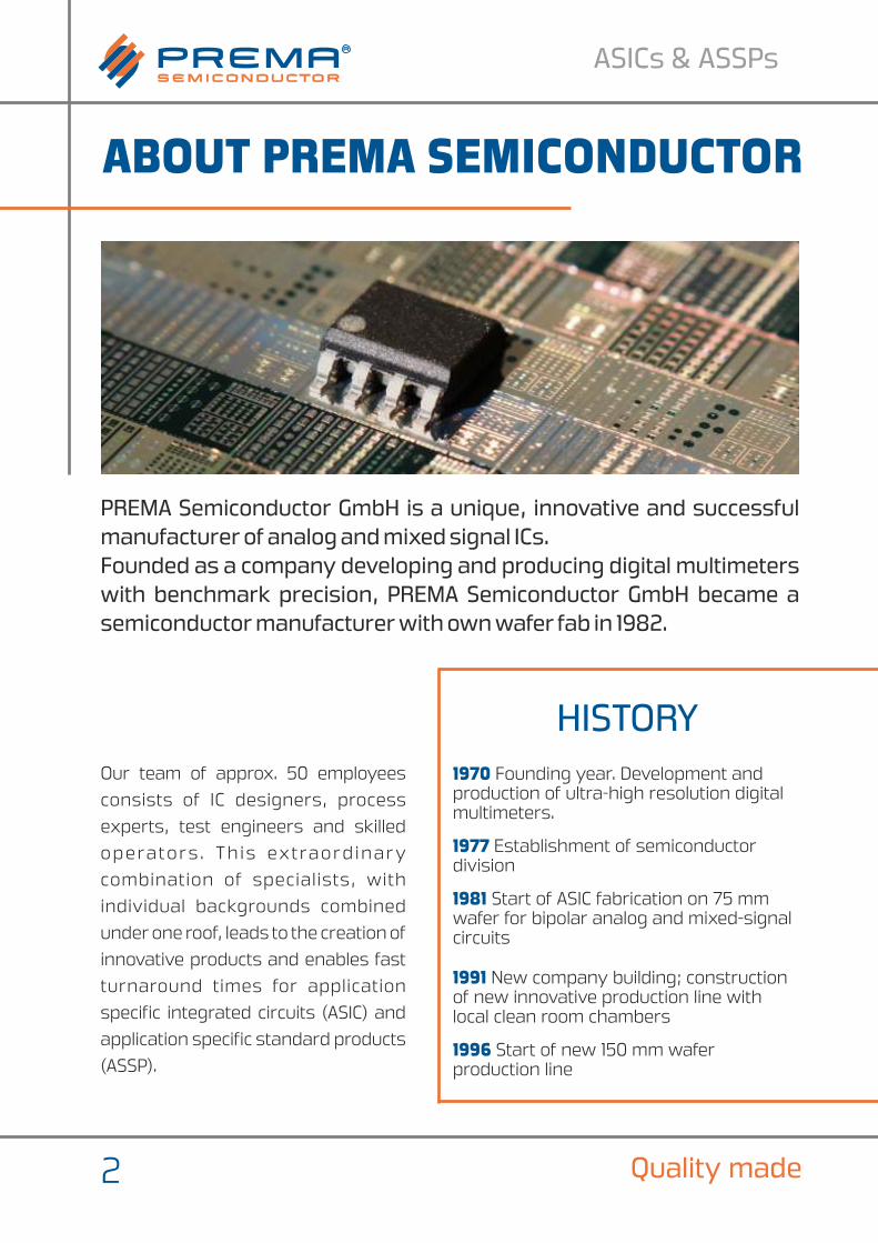
PREMA Semiconductor GmbH is a unique, innovative and successful manufacturer of analog and mixed signal ICs. Founded as a company developing and producing digital multimeters with benchmark precision, PREMA Semiconductor GmbH became a semiconductor manufacturer with own wafer fab in 1982.
Our team of approx. 50 employees
consists of IC designers, process
experts, test engineers and skilled
operators . Th is extraord inary
combination of specialists, with
individual backgrounds combined
under one roof, leads to the creation of
innovative products and enables fast
turnaround times for application
specific integrated circuits (ASIC) and
application specific standard products
(ASSP).
1970 Founding year. Development and production of ultra-high resolution digital multimeters.
1977 Establishment of semiconductor division
1981 Start of ASIC fabrication on 75 mm wafer for bipolar analog and mixed-signal circuits
1991 New company building; construction of new innovative production line with local clean room chambers
1996 Start of new 150 mm wafer production line
HISTORY

DESIGN & PRODUCTION
3in Germany
Design and Production in GermanyPREMA is a middle-sized, independent
company, located in Mainz, Germany,
close to Frankfurt airport.
This allows us to keep a close
relationship with our international
customer base.
With all critical development and
production steps in our headquarter
building, and with mostly German and
European suppliers of raw materials
and supportive services, we live on a
local eco-system, largely independent
of the big market players.
This strategy keeps the supply chain
manageable and the quality control-
lable.
It also allows us to consider extra-
ordinary requirements, to develop
special solutions and to react to our
customer’s needs in a flexible way.
1999 Introduction of the ModuS U6 process using high-voltage implantation, the new standard for high-voltage analog and mixed-signal ASICs.
2000 PREMA Precision Electronics becomes PREMA Semiconductor & ceased multimeter production
2004 High voltage NPN- and PNP- transistors (V > 120 V) introduced in CEo
ModuS U6 process
2012 Construction of new 200 mm wafer line
2013 Optical Encoders

4
CHIP DESIGN
It is our aim to make the electronics of your final product more competitive: smaller, more reliable, more economical. Our team of approximately ten IC designers is experienced in the development, simulation and layout of primarily analog ICs. They understand the needs of customers with analog circuits and can quickly develop concepts to put most of the circuitry into silicon.
To begin with, give us a rough sketch
of your idea. This may be in the form of
a general description, a block dia-
gram, or an equivalent solution. In
some cases you may already have a
specification or a schematic of an
already existing circuit.
Any of this should give us enough
ideas to propose a possible solution or
to start an open discussion with you.
This advice is free and without obliga-
tion. It is usually favourable to involve
How to Start an ASIC Project
our engineers as early as possible in
the design process.
ASICs & ASSPs
Quality made

5
Next Steps Towards the ASIC
After approving the specifica-tion, we will start the design process.We can perform or support you in all steps from the first concept sketch to series pro-duction.
In-house wafer production allows quick design loops in case that redesigns become necessary.
circuit specification and concept
circuit design and simulation
layout and design rule check
prototyping
design validation
series approval
production mask writing
development and validation of wafer-and IC-test
series wafer production
assembly in plastic package
DESIGN & PRODUCTION
in Germany
1. f
2. f
3.f
4.
5.
6.
7.h
8.55
9.5
10.

6
WAFERS MADE IN GERMANY
Based on advanced technologies, we manufacture analog and mixed-signal ASICs according to your specifications. Our fab is equipped with innovative production facilities and ready to produce your IC. From development to bulk production and testing of your ASIC – PREMA offers a complete service.
All process steps, including litho-
graphy, implantation, deposition of
isolators and metals, etching and
annealing steps are all available at our
facility.
The combination of a flexible wafer
processing facility and our ModuS U6
process, a unique method to replace
several conventional process steps by
one implantation, gives us an edge
against our competitors.
ASICs & ASSPs
Quality made

7
Versatile processPREMA‘s unique process replaces
three lithography layers, plus the
critical deposition of the epitaxial
layer, plus a long thermal oven step,
with just one layer using a well-
defined high-energy implantation.
This speeds up processing times and
reduces overall process costs.
This process, invented by PREMA has proven its qualities in many customer projects since then. It has been further developed to support not only bipolar devices, but also a triple-well BCD process with bipolar, CMOS and DMOS devices.
Radical simplification of process flow by 6 MeV high-enery ion implantation
Allows a large variety of components, such as NPN, PNP, JFET, photodiodes, phototransis- tors, implanted resistors, hall sensors
Low leakage currents allow a wide dynamic range for transistors
Unique process provides a high level of protection against reverse engineering and product copies
Advantages of the ModuS U6 Process
DESIGN & PRODUCTION
in Germany

®SEMIC CHAMBER TECHNOLOGY
8
A thorough compilation of production ®steps combined in one SEMIC cham-
ber guarantees optimum flexibility in
the face of changing process de-
mands and production volumes, at
the same time providing a fast and
reliable process flow. The status of
each wafer can be monitored centrally
at all times.
Autonomous local ultra-clean rooms, conceived and built by PREMA ®and called SEMIC chamber (Standard Electronic and Mechanical
Interface Clean Chamber) incorporate the best concepts regarding flexibility, economy and process optimization. This increases the yield and allows very rapid prototyping.
ASICs & ASSPs
Quality made

9
IC Test
For packaging, PREMA cooperates
with different partner in Europe and
Asia. This allows us to offer a wide
range of state-of-the-art packages.
This includes SOIC, TSSOP, QFN, SOT23,
but also optical packages or packages
with non-ferrous materials for
magnetic sensors.
Many of our customers assemble
chips on PCB directly from wafer.
After packaging, ICs undergo an additional test before being delivered in plastic tubes, tape and reel or trays.Alternatively, we can deliver bare dice on tested and inked wafers, or singulated dice on adhesive film.
IC PackagingAll ICs are tested on wafer level with
our fully automated wafer probers.
Test hardware and software for each
IC type is developed by our test
engineers to cover the full IC specifi-
cation. All tested parameters for each
IC are recorded and stored for best
traceability, and test data are regu-
larly evaluated statistically. The
project-specific IC test is comple-
mented by a measurement of the pro-
cess control module (PCM), monitoring
characteristic process data.
DESIGN & PRODUCTION
in Germany
PHOTODIODES
10
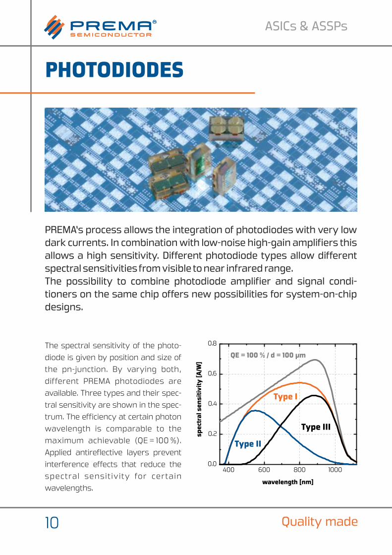
PREMA‘s process allows the integration of photodiodes with very low dark currents. In combination with low-noise high-gain amplifiers this allows a high sensitivity. Different photodiode types allow different spectral sensitivities from visible to near infrared range. The possibility to combine photodiode amplifier and signal condi-tioners on the same chip offers new possibilities for system-on-chip designs.
The spectral sensitivity of the photo-
diode is given by position and size of
the pn-junction. By varying both,
different PREMA photodiodes are
available. Three types and their spec-
tral sensitivity are shown in the spec-
trum. The efficiency at certain photon
wavelength is comparable to the
maximum achievable (QE = 100 %).
Applied antireflective layers prevent
interference effects that reduce the
spectral sensit iv ity for certain
wavelengths.
ASICs & ASSPs
Quality made

11
Optical EncodersOptical encoders measure rotations,
such as in robots, pumps, machine
tools or printers. PREMA sensor
modules for encoders combine the
capabilities of our photodiodes with
innovative ideas how to design the
sensor area, to offer a module that
allows high resolutions, is easy to
assemble, robust and versatile.
PREMA offers also encoder chips mounted on specially designed PCBs, with integra-ted reticle structure for lowest assembly cost or external reticle for best flexibility. Accessories such as LED-lens combos and glass disks can be delivered upon request.
Resolutions of up to 5000 increments
at 40 mm track diameter have been
realised. PREMA uses an innovative,
patented method to form sharp index
pulses.
Various combinations of encoder
tracks (e.g. with additional U/V/W
tracks) can be designed and produced
on demand.
DESIGN & PRODUCTION
in Germany

12
IC APPLICATIONS
PREMA Semiconductor GmbH offers state-of-the-art solutions for analog and mixed-signal circuits. Individual requirements of our customers have driven us to develop a wide range of unique and innovative products. Here we briefly outline some examples of ASICs developed over the last years.
Ambient light and sunload sensor for cars Photosensor, ampflifier and signal conditioner are placed on the same chip in a transparent DFN pack-age. Two versions are available: one for the near infrared, and one for the visible light range. High linearity and sensitivity are outstanding features of this small IC that is part of a sensor module fitted on the dashboard of many cars.
Monolithic infrared remote control receiver This ASIC is a fully integrated IR receiver for remote control sys-tems, containing the infrared diode,
Sensor ICs
variable gain amplifier, bandpass filter, integrator and digital output stage. This configuration allows a very easy assembly in a tiny package. Filter and adaptive gain control give it an unmatched rejection of disturbing signals.
ASICs & ASSPs
Quality made

13
Analog circuits make life in your house more comfortable and safe.Analog ASICs by PREMA make these circuits more powerful, versatile and unique.
Transceiver for house installation bus Installation buses operate at voltages up to 50V, and their drivers have to draw currents up to 500mA. The ASIC designed in compliance with our customer‘s specification and contains all functions of the physical bus interface. PREMA‘s high voltage transistors are ideal for these re-quirements.
Safety and Comfort ICsIC for residual-current circuit break-ers A low-offset amplfier and rectifier measures the residual current and breaks the supply line in case of danger. Different methods of detec-ting the residual current can be used, based on our customer‘s know-how in this field.
Gas burner controller The ASIC supervises the flame by measuring the ion current. It also contains drivers to control valves and interfaces for keys and status displays.
ICs for smoke detectors A highly sensitive low-noise amplifier detects the light scattered by smoke. It is combined with control circuits that initiate the alarm and other actions.
DESIGN & PRODUCTION
in Germany

14
IC APPLICATIONS
ASICs can conceal the ideas and patented methods of our customers . The functions are hidden in silicon which is designed and produced exclusively for one party. You can specify ICs containing new ideas for which no standard ICs exist, or combine functions in a unique way.
Microphone amplifier The excellent analog performance of our transis-tors, including low noise and a wide dynamic range from pA to mA allow the amplification of small signals from microphones or other signal sources. The full benefit of an ASIC comes from the combination of different functions, such as power control, battery charg-ing, status display drivers etc., to build a system on chip.
Sound enhancement chip MZ-01 ®Together with the Speaten filter by
Dedekind R&D (Japan), MZ-01 makes small speakers, built into laptop computers, portable audio devices,
Sound Processing ICs
flatscreen or CRT TV sets or car stereo, sound like much larger speaker sys-tems. MZ-01 is a controlled amplifier combining low noise, low distortion and a wide supply voltage range designed for use with the Speaten filter.
ASICs & ASSPs
Quality made

15
Power Converter ASICs
Wherever things move, ana-log signals are present.With PREMA ASICs you can sense movements with differ-ent sensors, or control motion with motor controllers.
Battery charging IC A fast battery charge controller ASIC for NiMH batteries used in consumer products has been developed by PREMA Semiconductor. The charge control is based on a patented multiple ramp A/D conversion method that allows the recognition of dV/dt with a sen-sitivity of better than 0.5 mV/min. A noise suppression of more than 60 dB prevents an overcharging with ex-ceptional accuracy which guarantees a long battery lifetime, despite of high charging rates.
Buck converter for energy saving circuits With a minimum of external components this ASIC can convert a volutage of up to 65V at the input down to 5V or 3.3V which are conve-nient for typical standby circuits such as an IR receiver, a timer, or a micro-controller.The high-voltage performance allows to control chains of LEDs used for status display in standby mode, leading to a low current consumption from the mains.
Motion Sensor ASICsHall effect sensor IC The PREMA process can integrate Hall effect sen-sors without requiring additional pro-cess layers. The high sensitivity of the Hall elements and the low offset of the following instrumentation amplifiers allow a low detection threshold of a magnetic motion sensor IC.
Incremental optical encoder chips A sensor with fine structures and an innovative method to generate sharp and precise Z channel pulses allows the construction of rotary encoders that are quick to assemble, reliable in operation and having a high resolu-tion.
DESIGN & PRODUCTION
in Germany

16Quality made in Germany
Circuits with standard ICs are simple
to steal. The basic idea of an ASIC is to
embed part of your system know-how
and to obtain a unique selling point for
your product. With ASICs made in con-
ventional processes counterfeits are
more difficult, yet still possible.
COPY-PROTECTED BY PROCESS
The unique features of PREMA’s
process, not available in other lines,
make it near impossible to copy your
circuit: copy protection by process.
Key is the choice of a trusted coopera-
tion partner for design and produc-
tion.
PREMA is a mid-sized independent
company, located in Mainz (Germany),
and all design and production facilities
are combined under one roof.
Together with the unique fabrication
process that makes reverse engi-
neering for competitors almost im-
possible and your know-how is pro-
tected against product piracy.
PREMA Semiconductor GmbHRobert-Bosch-Str. 655129 MainzGermanyPhone: +49-6131-5062-0Fax: +49-6131-5062-220Email: [email protected]
© 2014 PREMA Semiconductor GmbHDisclaimer: Information provided by PREMA is believed to be accurate and correct. However, no responsibility is assumed by PREMA for its use, nor for any infringements of patents or other rights of third parties which may result from its use. PREMA reserves the right at any time without notice to change services, data, or specifications.Edition w44/2014
Top Related