


Languages
Pages
Legal

FS84/FS85CFail-safe system basis chip with multiple SMPS and LDORev. 6 — 11 August 2020 Product data sheet
1 General description
The FS85/FS84 device family is developed in compliance with ASIL D process, FS84is ASIL B capable and FS85 is ASIL D capable. All device options are pin to pin andsoftware compatible.
The FS85/FS84 is an automotive functionally safe multi-output power supply integratedcircuit, with focus on Radar, Vision, ADAS domain controller, Radio and Infotainmentapplications. It includes multiple switch mode and linear voltage regulators. It offersexternal frequency synchronization input and output, for optimized system EMCperformance.
The FS85/FS84 includes enhanced safety features, with fail-safe output, becoming a fullpart of a safety-oriented system partitioning, covering both ASIL B and ASIL D safetyintegrity level. It is developed in compliance with ISO 26262 standard and is qualified incompliance with AEC-Q100 rev H (Grade1, MSL3).
Several device versions are available, offering choice in number of output rails, outputvoltage setting, operating frequency and power up sequencing, to address multipleapplications.
2 Features and benefits
• 60 V DC maximum input voltage for 12 V and 24 V applications• VPRE synchronous buck controller with external MOSFETs. Configurable output
voltage, switching frequency, and current capability up to 10 A peak.• Low voltage integrated synchronous BUCK1 converter, dedicated to MCU core supply
with SVS capability. Configurable output voltage and current capability up to 3.6 Apeak.
• Based on device options (see Table 1): low voltage integrated synchronous BUCK2converter. Configurable output voltage and current capability up to 3.6 A peak. Multi-phase capability with BUCK1 to extend the current capability up to 7.2 A peak on asingle rail. Static voltage scaling capability.
• Based on device options (see Table 1): low voltage integrated synchronous BUCK3converter. Configurable output voltage and current capability up to 3.6 A peak.
• BOOST converter with integrated low-side switch. Configurable output voltage and maxinput current up to 1.5 A peak.
• EMC optimization techniques including SMPS frequency synchronization, spreadspectrum, slew rate control, manual frequency tuning
• 2x linear voltage regulators for MCU IOs and ADC supply, external physical layer.Configurable output voltage and current capability up to 400 mA DC.
• OFF mode (power down) with very low quiescent current (10 µA typ)• 2x input pins for wake-up detection and battery voltage sensing• Device control via 32 bits SPI or I2C interface with CRC
NXP Semiconductors FS84/FS85CFail-safe system basis chip with multiple SMPS and LDO
FS84_FS85C All information provided in this document is subject to legal disclaimers. © NXP B.V. 2020. All rights reserved.
Product data sheet Rev. 6 — 11 August 20202 / 177
• Power synchronization pin to operate 2x FS85 devices or FS85 plus an external PMIC• Scalable portfolio from ASIL B to ASIL D with independent monitoring circuitry,
dedicated interface for MCU monitoring, simple and challenger watchdog function,power good, reset and interrupt, built-in self-test, fail-safe output
• Configuration by OTP programming. Prototype enablement to support custom settingduring project development in engineering mode.
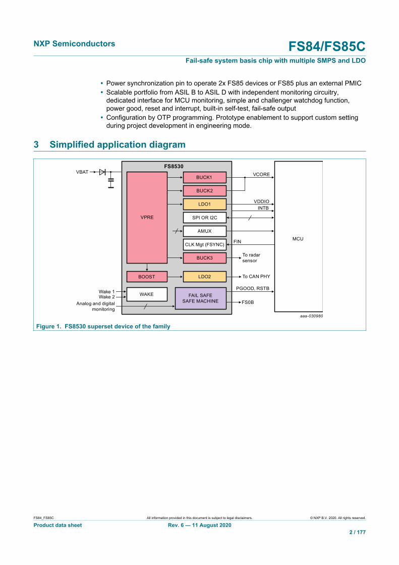
3 Simplified application diagram
aaa-030980
VBATFS8530
BUCK1
BUCK2
BUCK3 To radarsensor
To CAN PHY
LDO1
LDO2
VCORE
VDDIOINTB
SPI OR I2C
AMUX
CLK Mgt (FSYNC)
VPRE
MCU
WAKEWake 1Wake 2
Analog and digitalmonitoring
BOOST
FAIL SAFESAFE MACHINE
PGOOD, RSTB
FIN
FS0B
Figure 1. FS8530 superset device of the family
NXP Semiconductors FS84/FS85CFail-safe system basis chip with multiple SMPS and LDO
FS84_FS85C All information provided in this document is subject to legal disclaimers. © NXP B.V. 2020. All rights reserved.
Product data sheet Rev. 6 — 11 August 20203 / 177
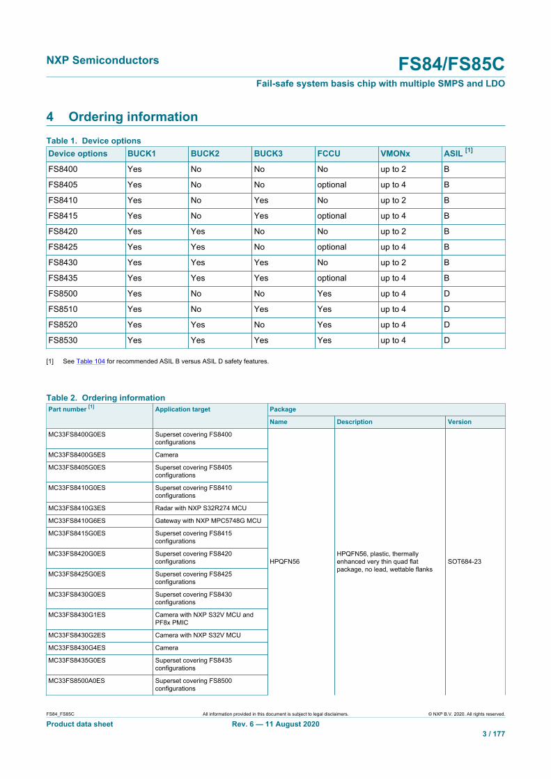
4 Ordering informationTable 1. Device optionsDevice options BUCK1 BUCK2 BUCK3 FCCU VMONx ASIL [1]
FS8400 Yes No No No up to 2 B
FS8405 Yes No No optional up to 4 B
FS8410 Yes No Yes No up to 2 B
FS8415 Yes No Yes optional up to 4 B
FS8420 Yes Yes No No up to 2 B
FS8425 Yes Yes No optional up to 4 B
FS8430 Yes Yes Yes No up to 2 B
FS8435 Yes Yes Yes optional up to 4 B
FS8500 Yes No No Yes up to 4 D
FS8510 Yes No Yes Yes up to 4 D
FS8520 Yes Yes No Yes up to 4 D
FS8530 Yes Yes Yes Yes up to 4 D
[1] See Table 104 for recommended ASIL B versus ASIL D safety features.
Table 2. Ordering informationPackagePart number [1] Application target
Name Description Version
MC33FS8400G0ES Superset covering FS8400configurations
MC33FS8400G5ES Camera
MC33FS8405G0ES Superset covering FS8405configurations
MC33FS8410G0ES Superset covering FS8410configurations
MC33FS8410G3ES Radar with NXP S32R274 MCU
MC33FS8410G6ES Gateway with NXP MPC5748G MCU
MC33FS8415G0ES Superset covering FS8415configurations
MC33FS8420G0ES Superset covering FS8420configurations
MC33FS8425G0ES Superset covering FS8425configurations
MC33FS8430G0ES Superset covering FS8430configurations
MC33FS8430G1ES Camera with NXP S32V MCU andPF8x PMIC
MC33FS8430G2ES Camera with NXP S32V MCU
MC33FS8430G4ES Camera
MC33FS8435G0ES Superset covering FS8435configurations
MC33FS8500A0ES Superset covering FS8500configurations
HPQFN56HPQFN56, plastic, thermallyenhanced very thin quad flatpackage, no lead, wettable flanks
SOT684-23

NXP Semiconductors FS84/FS85CFail-safe system basis chip with multiple SMPS and LDO
FS84_FS85C All information provided in this document is subject to legal disclaimers. © NXP B.V. 2020. All rights reserved.
Product data sheet Rev. 6 — 11 August 20204 / 177
PackagePart number [1] Application target
Name Description Version
MC33FS8510A0ES Superset covering FS8510configurations
MC33FS8510A2ES Domain controller
MC33FS8510D3ES Battery monitoring system
MC33FS8520A0ES Superset covering FS8520configurations
MC33FS8530A0ES Superset covering FS8530configurations
MC33FS8530A1ES Camera
MC33FS8530A4ES Imaging radar with NXP S32R MCU
[1] To order parts in tape and reel, add the R2 suffix to the part number.
A0 and G0 parts are non-programmed OTP configurations. Pre-programmed OTPconfigurations (other than BUCK regulators and ASIL level) are managed through partnumber extension: A1 to FZ for FS85 and G1 to LZ for FS84.
For a custom OTP configuration, please contact you local NXP sales representative.
4.1 Main OTP flavorsMC33FS8530A1ES
MC33FS8510A2ES
MC33FS8510D3ES
MC33FS8530A4ES
MC33FS8430G1ES
MC33FS8430G2ES
MC33FS8410G3ES
MC33FS8430G4ES
MC33FS8400G5ES
MC33FS8410G6ES
VPRE
Output voltage 3.3 V 3.3 V 5.0 V 4.1 V 4.1 V 5.0 V 3.3 V 4.1 V 3.3 V 3.3 V
Slopecompensation
60 mV/µs 140 mV/µs 60 mV/µs 70 mV/µs 70 mV/µs 70 mV/µs 140 mV/µs 100mV/µs 60mV/µs 60 mV/µs
Current limitation 120 mV 120 mV 50 mV 150 mV 150 mV 150 mV 120 mV 80 mV 150 mV 120 mV
High-side slewrate
PU/PD/900 mA PU/PD/900 mA PU/PD/900 mA PU/PD/130 mA PU/PD/130 mA PU/PD/130 mA PU/PD/130 mA PU/PD/900 mA PU/PD/130 mA PU/PD/130 mA
Switchingfrequency
455 kHz (ForcePWM)
455 kHz (ForcePWM)
455 kHz (ForcePWM)
455 kHz (ForcePWM)
455 kHz (ForcePWM)
455 kHz (ForcePWM)
455 kHz (ForcePWM)
455 kHz (ForcePWM)
455 kHz (ForcePWM)
455 kHz (ForcePWM)
Phase shifting delay 0 delay 0 delay 0 delay 0 delay 0 delay 0 delay 3 delay 0 delay 0 delay 0
Turn OFF delay 250 µs 250 µs 250µs 250 µs 32 ms 250 µs 250 µs 250 µs 250 µs 250 µs
VBOOST
Enabled Yes Yes Yes Yes Yes Yes Yes Yes Yes Yes
Output voltage 5.0 V 5.0 V 5.74 V 5.0 V 5.0 V 5.74 V 5.74 V 5.74 V 5.74 V 5.0 V
Slopecompensation
160 mV/µs 79 mV/µs 125 mV/µs 125 mV/µs 160 mV/µs 160 mV/µs 160 mV/µs 125 mV/µs 160 mV/µs 160 mV/µs
Slew rate 500 V/µs 500 V/µs 300 V/µs 500 V/µs 500 V/µs 500 V/µs 500 V/µs 500 V/µs 500 V/µs 500 V/µs
Compensationresistor
750 kΩ 750 kΩ 750 kΩ 750 kΩ 750 kΩ 750 kΩ 750 kΩ 750 kΩ 750 kΩ 750 kΩ
Compensationcapacitor
125 pF 125 pF 125 pF 125 pF 125 pF 125 pF 125 pF 125 pF 125 pF 125 pF
Switchingfrequency
2.22 MHz 2.22 MHz 2.22 MHz 2.22 MHz 2.22 MHz 2.22 MHz 2.22 MHz 2.22 MHz 2.22 MHz 2.22 MHz
Phase shifting delay 1 delay 0 delay 1 delay 0 delay 0 delay 0 delay 0 delay 7 delay 0 delay 3
Behavior in caseof TSD
BOOSTshutdown + DFS
BOOSTshutdown + DFS
BOOSTshutdown + DFS
BOOSTshutdown
BOOSTshutdown
BOOSTshutdown
BOOSTshutdown
BOOSTshutdown
BOOSTshutdown
BOOSTshutdown
BUCK1
Output voltage 1.35 V 1.025 V 1.3 V 1.1 V 1.8 V 1.1 V 1.25 V 1.03125 V 1.25 V 1.2 V
Current limitation 2.6 A 2.6 A 2.6 A 4.5 A 4.5 A 4.5 A 4.5 A 4.5 A 2.6 A 2.6 A
Inductor 1.5 µH 1 µH 1 µH 1 µH 1 µH 1 µH 1 µH 1 µH 1 µH 1 µH
Compensationnetwork
65 GM 65 GM 65 GM 65 GM 65 GM 65 GM 65 GM 65 GM 65 GM 65 GM
Switchingfrequency
2.22 MHz 2.22 MHz 2.22 MHz 2.22 MHz 2.22 MHz 2.22 MHz 2.22 MHz 2.22 MHz 2.22 MHz 2.22 MHz
Phase shifting delay 3 delay 0 delay 2 delay 0 delay 0 delay 0 delay 0 delay 0 delay 0 delay 2
Behavior in caseof TSD
BUCK1 shutdown+ DFS
BUCK1 shutdown+ DFS
BUCK1 shutdown+ DFS
BUCK1 shutdown BUCK1 shutdown BUCK1 shutdown BUCK1 shutdown BUCK1 shutdown+ DFS
BUCK1 shutdown+ DFS
BUCK1 shutdown
Powersequencing slot
Regulator Startand Stop in Slot 1
Regulator Startand Stop in Slot 0
Regulator Startand Stop in Slot 0
Regulator Startand Stop in Slot 6
Regulator Startand Stop in Slot 0
Regulator Startand Stop in Slot 6
Regulator Startand Stop in Slot 1
Regulator Startand Stop in Slot 4
Regulator Startand Stop in Slot 0
Regulator Startand Stop in Slot 0

NXP Semiconductors FS84/FS85CFail-safe system basis chip with multiple SMPS and LDO
FS84_FS85C All information provided in this document is subject to legal disclaimers. © NXP B.V. 2020. All rights reserved.
Product data sheet Rev. 6 — 11 August 20205 / 177
MC33FS8530A1ES
MC33FS8510A2ES
MC33FS8510D3ES
MC33FS8530A4ES
MC33FS8430G1ES
MC33FS8430G2ES
MC33FS8410G3ES
MC33FS8430G4ES
MC33FS8400G5ES
MC33FS8410G6ES
DVS (Soft start) 7.81 mV/µs 7.81 mV/µs 7.81 mV/µs 7.81 mV/µs 7.81 mV/µs 7.81 mV/µs 7.81 mV/µs 7.81 mV/µs 7.81 mV/µs 7.81 mV/µs
BUCK2
Enabled Yes No No Yes No Yes No Yes No No
Output voltage 1.8 V 1.25 V 1.35 V 1.8 V 1.25 V 1.8 V 1.25 V 1.03125 V 1.25 V 1.2 V
Current limitation 4.5 A 4.5 A 4.5 A 4.5 A 4.5 A 4.5 A 4.5 A 4.5 A 4.5 A 4.5 A
Inductor 1.5 µH 1 µH 1 µH 1 µH 1 µH 1 µH 1 µH 1 µH 1 µH 1 µH
Compensationnetwork
65 GM 65 GM 65 GM 65 GM 65 GM 65 GM 65 GM 65 GM 65 GM 65 GM
Switchingfrequency
2.22 MHz 2.22 MHz 2.22 MHz 2.22 MHz 2.22 MHz 2.22 MHz 2.22 MHz 2.22 MHz 2.22 MHz 2.22 MHz
Multiphase withBuck1
No No No No No No No Yes No No
Phase shifting delay 2 delay 0 delay 4 delay 0 delay 0 delay 0 delay 3 delay 4 delay 4 delay 7
Behavior in caseof TSD
BUCK2 shutdown+ DFS
BUCK2 shutdown BUCK2 shutdown+ DFS
BUCK2 shutdown BUCK2 shutdown BUCK2 shutdown BUCK2 shutdown BUCK2 shutdown+ DFS
BUCK2 shutdown BUCK2 shutdown
Powersequencing slot
Regulator Startand Stop in Slot 0
Regulator Startand Stop in Slot 0
Regulatordoes not Start(Enabled by SPI)
Regulator Startand Stop in Slot 4
Regulatordoes not Start(Enabled by SPI)
Regulator Startand Stop in Slot 2
RegulatorDoes not Start(Enabled by SPI)
Regulator Startand Stop in Slot 4
Regulatordoes not Start(Enabled by SPI)
Regulatordoes not Start(Enabled by SPI)
DVS (Soft start) 7.81 mV/µs 7.81 mV/µs 7.81 mV/µs 7.81 mV/µs 7.81 mV/µs 7.81 mV/µs 7.81 mV/µs 7.81 mV/µs 7.81 mV/µs 7.81 mV/µs
BUCK3
Enabled Yes Yes Yes Yes Yes Yes Yes Yes No Yes
Output voltage 1.2 V 1.8 V 3.3 V 3.3 V 3.3 V 3.3 V 2.3 V 1.35 V 1.8 V 1.8 V
Inductor 1.5 µH 1 µH 1 µH 1 µH 1 µH 1 µH 1 µH 1 µH 1 µH 1 µH
Current limitation 2.6 A 2.6 A 2.6 A 4.5 A 4.5 A 4.5 A 4.5 A 2.6 A 4.5 A 2.6 A
Compensationresistor
Default Default Default Default Default Default Default Default Default Default
Gain control Default Default Default Default Default Default Default Default Default Default
Switchingfrequency
2.22 MHz 2.22 MHz 2.22 MHz 2.22 MHz 2.22 MHz 2.22 MHz 2.22 MHz 2.22 MHz 2.22 MHz 2.22 MHz
Phase shifting delay 7 delay 0 delay 3 delay 0 delay 0 delay 0 delay 0 delay 2 delay 0 delay 4
Behavior in caseof TSD
BUCK3 shutdown+ DFS
BUCK3 shutdown+ DFS
BUCK3 shutdown+ DFS
BUCK3 shutdown BUCK3 shutdown BUCK3 shutdown BUCK3 shutdown BUCK3 shutdown+ DFS
BUCK3 shutdown BUCK3 shutdown
Powersequencing slot
Regulator Startand Stop in Slot 6
Regulator Startand Stop in Slot 6
Regulator Startand Stop in Slot 1
Regulator Startand Stop in Slot 0
Regulator Startand Stop in Slot 0
Regulator Startand Stop in Slot 0
Regulator Startand Stop in Slot 0
Regulator Startand Stop in Slot 5
RegulatorDoes not Start(Enabled by SPI)
Regulator Startand Stop in Slot 0
DVS (Soft start) 10.41 mV/µs 10.41 mV/µs 10.41 mV/µs 10.41 mV/µs 10.41 mV/µs 10.41 mV/µs 10.41 mV/µs 10.41 mV/µs 10.41 mV/µs 10.41 mV/µs
LDO1
Output voltage 2.5 V 5.0 V 5. 0 V 1.8 V 1.8 V 1.2 V 3.3 V 3.3 V 5.0 V 1.8 V
Current limitation 400 mA 400 mA 150 mA 400 mA 400 mA 400 mA 150 mA 400 mA 400 mA 400 mA
Behavior in caseof TSD
LDO1 shutdown+ DFS
LDO1 shutdown LDO1 shutdown+ DFS
LDO1 shutdown LDO1 shutdown LDO1 shutdown LDO1 shutdown LDO1 shutdown+ DFS
LDO1 shutdown LDO1 shutdown
Powersequencing slot
Regulator Startand Stop in Slot 5
RegulatorDoes not Start(Enabled by SPI)
Regulator Startand Stop in Slot 2
Regulator Startand Stop in Slot 2
RegulatorDoes not Start(Enabled by SPI)
Regulator Startand Stop in Slot 4
Regulator Startand Stop in Slot 2
Regulator Startand Stop in Slot 6
Regulator Startand Stop in Slot 1
Regulatordoes not Start(Enabled by SPI)
LDO2
Output voltage 3.3 V 5.0 V 5.0 V 1.2 V 3.3 V 1.8 V 5.0 V 5.0 V 5.0 V 3.3 V
Current limitation 400 mA 400 mA 150 mA 400 mA 400 mA 400 mA 150 mA 150 mA 150 mA 400 mA
Behavior in caseof TSD
LDO2 shutdown+ DFS
LDO2 shutdown LDO2 shutdown+ DFS
LDO2 shutdown LDO2 shutdown LDO2 shutdown LDO2 shutdown LDO2 shutdown LDO2 shutdown LDO2 shutdown
Powersequencing slot
Regulator Startand Stop in Slot 2
Regulator Startand Stop in Slot 0
Regulator Startand Stop in Slot 3
Regulator Startand Stop in slot 1
Regulatordoes not Start(Enabled by SPI)
Regulator Startand Stop in Slot 2
Regulator Startand Stop in Slot 1
Regulator Startand Stop in Slot 3
Regulatordoes not Start(Enabled by SPI)
Regulatordoes not Start(Enabled by SPI)
Other
PSYNC Disabled Disabled Disabled Disabled 1x FS85 and 1xPF82
Disabled Disabled Disabled Disabled Disabled
PLL enabled Yes No No Yes No No Yes No No Yes
TSlot 250 µs 250 µs 250 µs 250 µs 250 µs 250 µs 250 µs 250 µs 250 µs 250 µs
Deep Fail-safe(autoretry)
Infinite Infinite Infinite Infinite Infinite Infinite x15 x15 x15 x15
VSUP power-upthreshold
4.9 V 4.9 V 6.2 V 4.9 V 4.9 V 4.9 V 4.9 V 4.9V 4.9 V 4.9 V
Regulatorassigned toVDDIO
LDO2 VPRE LDO1 BUCK3 BUCK3 External regulator VPRE LDO1 VPRE VPRE
I2C address 0x24 0x20 0x20 0x20 0x20 0x20 0x20 0x20 0x20 0x20
Device ID tbd tbd tbd tbd tbd tbd tbd tbd tbd tbd
NXP Semiconductors FS84/FS85CFail-safe system basis chip with multiple SMPS and LDO
FS84_FS85C All information provided in this document is subject to legal disclaimers. © NXP B.V. 2020. All rights reserved.
Product data sheet Rev. 6 — 11 August 20206 / 177
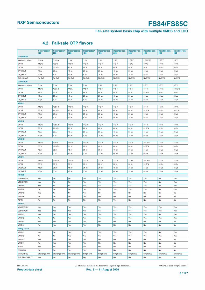
4.2 Fail-safe OTP flavorsMC33FS8530A1ES
MC33FS8510A2ES
MC33FS8510D3ES
MC33FS8530A4ES
MC33FS8430G1ES
MC33FS8430G2ES
MC33FS8410G3ES
MC33FS8430G4ES
MC33FS8400G5ES
MC33FS8410G6ES
VCOREMON
Monitoring voltage 1.35 V 1.025 V 1.3 V 1.1 V 1.8 V 1.1 V 1.25 V 1.03125 V 1.25 V 1.2 V
OVTH 112 % 109 % 110 % 112 % 112 % 112 % 112% 106% 110 % 110 %
UVTH 88 % 88.5 % 90 % 88 % 88 % 88% 88% 94% 90 % 95 %
OV_DGLT 45 µs 25 µs 45 µs 25 µs 25 µs 45 µs 25 µs 45 µs 25 µs 25 µs
UV_DGLT 40 us 5 µs 40 µs 5 µs 15 µs 40 µs 15 µs 40 µs 15 µs 15 µs
SVS_CLAMP No SVS No SVS No SVS No SVS No SVS No SVS No SVS No SVS No SVS No SVS
VDDIOMON
Monitoring voltage 3.3 V 3.3 V 5.0 V 3.3 V 3.3 V 3.3 V 3.3 V 3.3 V 3.3 V 3.3 V
OVTH 112 % 106.5 % 110% 112 % 112 % 112 % 112 % 107 % 110 % 106.5 %
UVTH 88 % 93 % 90 % 88 % 88 % 88 % 88 % 93.5 % 90 % 95 %
OV_DGLT 45 µs 25 µs 45 µs 25 µs 25 µs 45 µs 25 µs 45 µs 25 µs 25 µs
UV_DGLT 40 µs 5 µs 40 µs 5 µs 15 µs 40 µs 15 µs 40 µs 15 µs 15 µs
VMON1
OVTH 112 % 108.5 % 110 % 112 % 112 % 112 % 112 % 107 % 112 % 109 %
UVTH 88 % 91.5 % 90 % 88 % 88 % 88 % 88 % 92.5 % 88 % 95.5 %
OV_DGLT 45 µs 25 µs 45 µs 25 µs 25 µs 45 µs 25 µs 45 µs 25 µs 25 µs
UV_DGLT 40 µs 5 µs 40 µs 5 µs 15 µs 40 µs 15 µs 40 µs 15 µs 15 µs
VMON2
OVTH 112 % 108.5 % 110 % 112 % 112 % 112 % 112 % 107 % 108 % 110 %
UVTH 88 % 91.5 % 90 % 88 % 88 % 88 % 88 % 92.5 % 92 % 90 %
OV_DGLT 45 µs 25 µs 45 µs 25 µs 25 µs 45 µs 25 µs 45 µs 25 µs 25 µs
UV_DGLT 40 µs 5 µs 40 µs 5 µs 15 µs 40 µs 15 µs 40 µs 15 µs 15 µs
VMON3
OVTH 112 % 107 % 110 % 112 % 112 % 112 % 112 % 104.5 % 112 % 112 %
UVTH 88 % 91.5 % 90 % 88 % 88 % 88 % 88 % 95.5 % 88 % 88 %
OV_DGLT 45 µs 25 µs 45 µs 25 µs 25 µs 45 µs 25 µs 45 µs 25 µs 25 µs
UV_DGLT 40 µs 5 µs 40 µs 5 µs 15 µs 40 µs 15 µs 40 µs 15 µs 15 µs
VMON4
OVTH 112 % 107.5 % 110 % 112 % 112 % 112 % 11 2% 104.5 % 112 % 112 %
UVTH 88 % 91 % 90 % 88 % 88 % 88 % 88 % 95.5 % 88 % 88 %
OV_DGLT 45 µs 25 µs 45 µs 25 µs 25 µs 45 µs 25 µs 45 µs 25 µs 25 µs
UV_DGLT 40 µs 5 µs 40 µs 5 µs 15 µs 40 µs 15 µs 40 µs 15 µs 15 µs
PGOOD
VCOREMON Yes No No Yes Yes Yes Yes Yes No Yes
VDDIOMON Yes No No Yes Yes Yes Yes Yes No Yes
VMON1 Yes No No Yes Yes Yes Yes Yes No Yes
VMON2 No No No Yes Yes Yes Yes Yes No Yes
VMON3 Yes No No Yes No No No No No No
VMON4 No No No Yes No No No No No No
RSTB No No No No No Yes No No No No
ABIST1
VCOREMON Yes Yes Yes Yes Yes Yes Yes Yes Yes Yes
VDDIOMON Yes Yes Yes Yes Yes Yes Yes Yes Yes Yes
VMON1 Yes No Yes Yes Yes Yes Yes Yes No Yes
VMON2 No No Yes Yes Yes Yes Yes Yes Yes Yes
VMON3 Yes Yes Yes Yes No No No No No No
VMON4 No Yes Yes Yes No No No No No No
Safety enable
VMON1 Yes No Yes Yes Yes Yes Yes Yes No Yes
VMON2 No No Yes Yes Yes Yes Yes Yes Yes Yes
VMON3 Yes Yes Yes Yes No No No No No No
VMON4 No Yes Yes Yes No No No No No No
FCCU Yes No No Yes No No No No No No
ERRMON No No Yes Yes No No No No No No
WATCHDOG Challenger WD Challenger WD Challenger WD Simple WD Simple WD Simple WD Simple WD Simple WD Simple WD Simple WD
FLT_RECOVERY Yes No No No No No No No No No

NXP Semiconductors FS84/FS85CFail-safe system basis chip with multiple SMPS and LDO
FS84_FS85C All information provided in this document is subject to legal disclaimers. © NXP B.V. 2020. All rights reserved.
Product data sheet Rev. 6 — 11 August 20207 / 177
MC33FS8530A1ES
MC33FS8510A2ES
MC33FS8510D3ES
MC33FS8530A4ES
MC33FS8430G1ES
MC33FS8430G2ES
MC33FS8410G3ES
MC33FS8430G4ES
MC33FS8400G5ES
MC33FS8410G6ES
Other
I2C address 0x21 0x21 0x21 0x21 0x21 0x21 0x21 0x21 0x21 0x21
5 Applications
• Radar (corner radar, imaging radar, ...)• Vision (mono camera, stereo camera, night vision, ...)• ADAS domain controller• Infotainment• V2x
NXP Semiconductors FS84/FS85CFail-safe system basis chip with multiple SMPS and LDO
FS84_FS85C All information provided in this document is subject to legal disclaimers. © NXP B.V. 2020. All rights reserved.
Product data sheet Rev. 6 — 11 August 20208 / 177
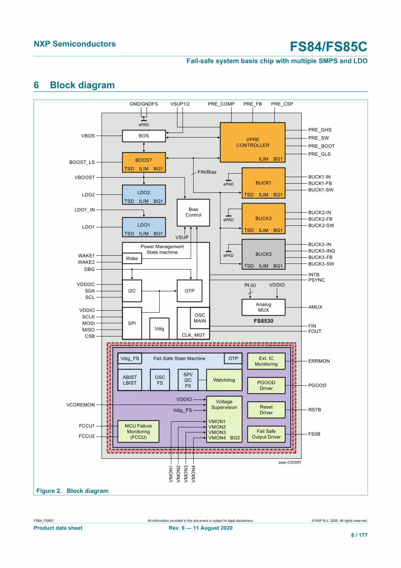
6 Block diagram
aaa-030981
Vdig_FS OTPFail-Safe State Machine
ABISTLBIST
CLK_MGT
BiasControl
Power ManagementState machine
Watchdog
MCU FailureMonitoring
(FCCU)
Ext. ICMonitoring
PGOODDriver
AnalogMUX
FS8530
ResetDriver
Fail SafeOutput Driver
VoltageSupervision
VDDIO
Vdig_FS
IN (s) VDDIO
VM
ON
1
VCOREMON
FCCU1
ERRMON
AMUX
BUCK3
ILIMTSD BG1 BUCK3-SWBUCK3-FBBUCK3-INQBUCK3-IN
VPRECONTROLLER
ILIM
FIN/Bias
BG1PRE_GLSPRE_BOOT
PRE_SW
PRE_GHS
MISOCSB
MOSISCLK
VDDIO
SCLSDA
VDDI2C
WAKE2WAKE1
LDO1
LDO1_IN
DBG
FINFOUT
INTBPSYNC
PGOOD
RSTB
FS0BFCCU2
VM
ON
2V
MO
N3
VM
ON
4
OSCFS
OSCMAINSPI
I2C
Wake
VSUP
ePAD
Vdig
OTP
SPI/I2CFS
VMON1VMON2VMON3VMON4 BG2
BUCK2
ILIMTSD BG1LDO1
ILIMTSD BG1
LDO2
VBOOST
LDO2
ILIMTSD BG1
BOOST_LS BOOST
VBOS BOS
ILIMTSD BG1
BUCK2-SWBUCK2-FBBUCK2-IN
ePAD
BUCK1
ILIMTSD BG1BUCK1-SWBUCK1-FBBUCK1-IN
ePAD
ePAD
GND/GNDFS VSUP1/2 PRE_CSPPRE_COMP PRE_FB
Figure 2. Block diagram
NXP Semiconductors FS84/FS85CFail-safe system basis chip with multiple SMPS and LDO
FS84_FS85C All information provided in this document is subject to legal disclaimers. © NXP B.V. 2020. All rights reserved.
Product data sheet Rev. 6 — 11 August 20209 / 177
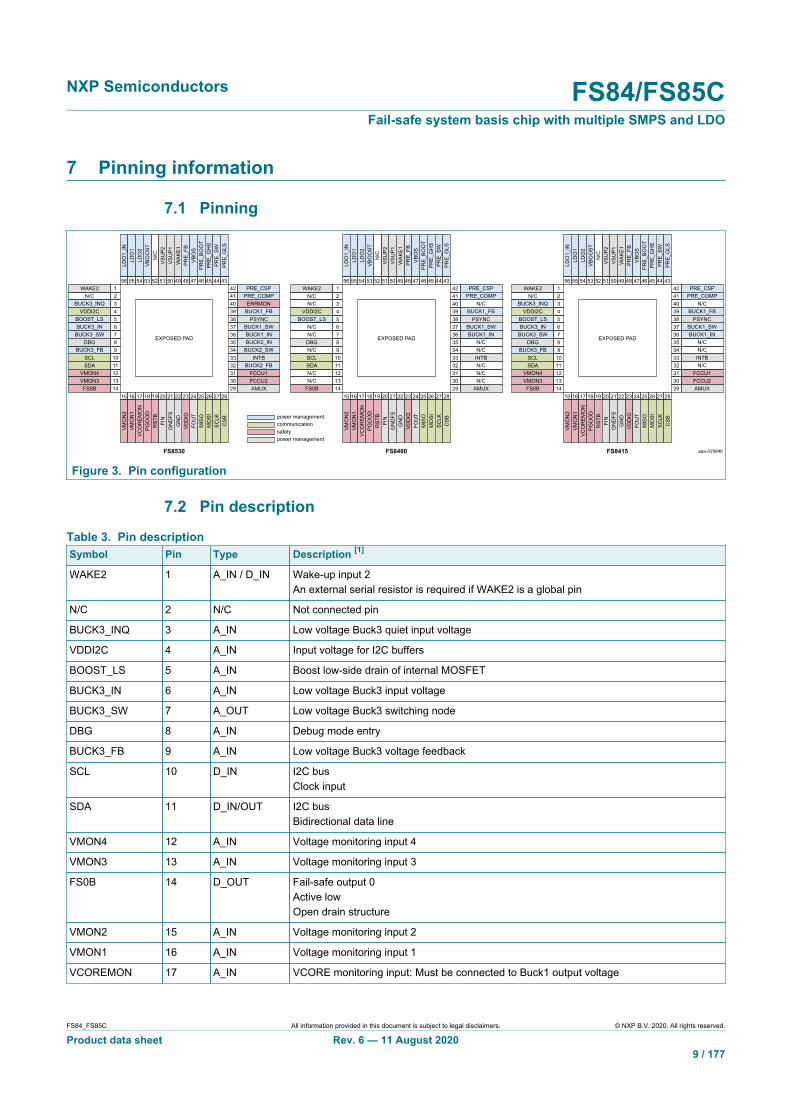
7 Pinning information
7.1 Pinning
WAKE2 1N/C 2
BUCK3_INQ 3VDDI2C 4
BOOST_LS 5BUCK3_IN 6
BUCK3_SW 7DBG 8
BUCK3_FB 9SCL 10SDA 11
VMON4 12VMON3 13FS0B 14
15 16 17 18 19 20 21 22 23 24 25 26 27 28
56 55 54 53 52 51 50 49 48 47 46 45 44 43PRE_CSP42
PRE_COMP41ERRMON40
BUCK1_FB39PSYNC38
BUCK1_SW37BUCK1_IN
EXPOSED PAD36
BUCK2_IN35BUCK2_SW34
INTB33BUCK2_FB32
FCCU131FCCU230AMUX
power management
VMO
N2
VMO
N1
VCO
REM
ON
PGO
OD
RST
BFI
NG
ND
FSG
ND
VDD
IOFO
UT
MIS
OM
OSI
SCLK
CSB
LDO
1_IN
LDO
1LD
O2
VBO
OST
N/C
VSU
P2VS
UP1
WAK
E1PR
E_FB
VBO
SPR
E_BO
OT
PRE_
GH
SPR
E_SW
PRE_
GLS
29
communicationsafetypower management
WAKE2 1N/C 2N/C 3
VDDI2C 4BOOST_LS 5
N/C 6N/C 7DBG 8N/C 9SCL 10SDA 11N/C 12N/C 13
FS0B 1415 16 17 18 19 20 21 22 23 24 25 26 27 28
56 55 54 53 52 51 50 49 48 47 46 45 44 43PRE_CSP42
PRE_COMP41N/C40
BUCK1_FB39PSYNC38
BUCK1_SW37BUCK1_IN
EXPOSED PAD
FS8530 FS8400
36N/C35N/C34INTB33N/C32N/C31N/C30
AMUX
VMO
N2
VMO
N1
VCO
REM
ON
PGO
OD
RST
BFI
NG
ND
FSG
ND
VDD
IOFO
UT
MIS
OM
OSI
SCLK
CSB
LDO
1_IN
LDO
1LD
O2
VBO
OST
N/C
VSU
P2VS
UP1
WAK
E1PR
E_FB
VBO
SPR
E_BO
OT
PRE_
GH
SPR
E_SW
PRE_
GLS
29
aaa-035646
WAKE2 1N/C 2
BUCK3_INQ 3VDDI2C 4
BOOST_LS 5BUCK3_IN 6
BUCK3_SW 7DBG 8
BUCK3_FB 9SCL 10SDA 11
VMON4 12VMON3 13FS0B 14
15 16 17 18 19 20 21 22 23 24 25 26 27 28
56 55 54 53 52 51 50 49 48 47 46 45 44 43PRE_CSP42
PRE_COMP41N/C40
BUCK1_FB39PSYNC38
BUCK1_SW37BUCK1_IN
EXPOSED PAD
FS8415
36N/C35N/C34
INTB33N/C32
FCCU131FCCU230AMUX
VMO
N2
VMO
N1
VCO
REM
ON
PGO
OD
RST
BFI
NG
ND
FSG
ND
VDD
IOFO
UT
MIS
OM
OSI
SCLK
CSB
LDO
1_IN
LDO
1LD
O2
VBO
OST
N/C
VSU
P2VS
UP1
WAK
E1PR
E_FB
VBO
SPR
E_BO
OT
PRE_
GH
SPR
E_SW
PRE_
GLS
29
Figure 3. Pin configuration
7.2 Pin description
Table 3. Pin descriptionSymbol Pin Type Description [1]
WAKE2 1 A_IN / D_IN Wake-up input 2An external serial resistor is required if WAKE2 is a global pin
N/C 2 N/C Not connected pin
BUCK3_INQ 3 A_IN Low voltage Buck3 quiet input voltage
VDDI2C 4 A_IN Input voltage for I2C buffers
BOOST_LS 5 A_IN Boost low-side drain of internal MOSFET
BUCK3_IN 6 A_IN Low voltage Buck3 input voltage
BUCK3_SW 7 A_OUT Low voltage Buck3 switching node
DBG 8 A_IN Debug mode entry
BUCK3_FB 9 A_IN Low voltage Buck3 voltage feedback
SCL 10 D_IN I2C busClock input
SDA 11 D_IN/OUT I2C busBidirectional data line
VMON4 12 A_IN Voltage monitoring input 4
VMON3 13 A_IN Voltage monitoring input 3
FS0B 14 D_OUT Fail-safe output 0Active lowOpen drain structure
VMON2 15 A_IN Voltage monitoring input 2
VMON1 16 A_IN Voltage monitoring input 1
VCOREMON 17 A_IN VCORE monitoring input: Must be connected to Buck1 output voltage

NXP Semiconductors FS84/FS85CFail-safe system basis chip with multiple SMPS and LDO
FS84_FS85C All information provided in this document is subject to legal disclaimers. © NXP B.V. 2020. All rights reserved.
Product data sheet Rev. 6 — 11 August 202010 / 177
Symbol Pin Type Description [1]
PGOOD 18 D_OUT Power good outputActive lowPull up to VDDIO mandatory
RSTB 19 D_OUT Reset outputActive lowThe main function is to reset the MCU. Reset input voltage is monitored to detect externalreset and fault condition.Pull up to VDDIO mandatory
FIN 20 D_IN Frequency synchronization input
GNDFS 21 GND Fail-safe ground
GND 22 GND Main ground
VDDIO 23 A_IN Input voltage for SPI, FOUT and AMUX buffersAllow voltage compatibility with MCU I/Os
FOUT 24 D_OUT Frequency synchronization output
MISO 25 D_OUT SPI busMaster input slave output
MOSI 26 D_IN SPI busMaster output slave Input
SCLK 27 D_IN SPI busClock input
CSB 28 D_IN Chip select (active low)
AMUX 29 A_OUT Multiplexed output to connect to MCU ADCSelection of the analog parameter through SPI or I2C
FCCU2 30 D_IN MCU error monitoring input 2
FCCU1 31 D_IN MCU error monitoring input 1
BUCK2_FB 32 A_IN Low voltage Buck2 voltage feedback
INTB 33 D_OUT Interrupt output
BUCK2_SW 34 A_OUT Low voltage Buck2 switching node
BUCK2_IN 35 A_IN Low voltage Buck2 input voltage
BUCK1_IN 36 A_IN Low voltage Buck1 input voltage
BUCK1_SW 37 A_OUT Low voltage Buck1 switching node
PSYNC 38 D_IN/OUT Power synchronization input/output
BUCK1_FB 39 A_IN Low voltage Buck1 voltage feedback
ERRMON 40 D_IN External IC error monitoring input
PRE_COMP 41 A_IN VPRE compensation network
PRE_CSP 42 A_IN VPRE positive current sense input
PRE_GLS 43 A_OUT VPRE low-side gate driver for external MOSFET
PRE_SW 44 A_OUT VPRE switching node
PRE_GHS 45 A_OUT VPRE high-side gate driver for external MOSFET
PRE_BOOT 46 A_IN/OUT VPRE bootstrap capacitor
VBOS 47 A_OUT Best of supply output voltage
PRE_FB 48 A_IN VPRE voltage feedback and negative current sense input
WAKE1 49 A_IN / D_IN Wake up input 1An external serial resistor is required if WAKE1 is a global pin

NXP Semiconductors FS84/FS85CFail-safe system basis chip with multiple SMPS and LDO
FS84_FS85C All information provided in this document is subject to legal disclaimers. © NXP B.V. 2020. All rights reserved.
Product data sheet Rev. 6 — 11 August 202011 / 177
Symbol Pin Type Description [1]
VSUP1 50 A_IN Power supply 1 of the deviceAn external reverse battery protection diode in series is mandatory
VSUP2 51 A_IN Power supply 2 of the deviceAn external reverse battery protection diode in series is mandatory
N/C 52 N/C Not connected pin
VBOOST 53 A_IN VBOOST voltage feedback
LDO2 54 A_OUT Linear regulator 2 output voltage
LDO1 55 A_OUT Linear regulator 1 output voltage
LDO1_IN 56 A_IN Linear regulator 1 input voltage
EP 57 GND Expose pad (BUCK1, BUCK2 and BUCK3 low-side GNDs are connected to the exposepad)Must be connected to GND
[1] See Section 8 for connection of unused pins.
8 Connection of unused pinsTable 4. Connection of unused pinsPin Name Type Connection if not used
1 WAKE2 A_IN / D_IN External pull down to GND
2 N/C N/C Open
3 BUCK3_INQ A_IN Open
4 VDDI2C A_IN Open
5 BOOST_LS A_IN See Section 21.5 "VBOOST not populated"
6 BUCK3_IN A_IN Open
7 BUCK3_SW A_OUT Open
8 DBG A_IN Connection mandatory
9 BUCK3_FB A_IN Open – 1.5 MΩ internal resistor bridge pull down to GND
10 SCL D_IN External pull down to GND
11 SDA D_IN/OUT External pull down to GND
12 VMON4 A_IN Open – 2 MΩ internal pull down to GND, OTP_VMON4_EN = 0
13 VMON3 A_IN Open – 2 MΩ internal pull down to GND, OTP_VMON3_EN = 0
14 FS0B D_OUT Open – 2 MΩ internal pull down to GND
15 VMON2 A_IN Open – 2 MΩ internal pull down to GND, OTP_VMON2_EN = 0
16 VMON1 A_IN Open – 2 MΩ internal pull down to GND, OTP_VMON1_EN = 0
17 VCOREMON A_IN Connection mandatory
18 PGOOD D_OUT Connection mandatory
19 RSTB D_OUT Connection mandatory
20 FIN D_IN External pull down to GND
21 GNDFS GND Connection mandatory
22 GND GND Connection mandatory
23 VDDIO A_IN Connection mandatory
24 FOUT D_OUT Open – push pull structure

NXP Semiconductors FS84/FS85CFail-safe system basis chip with multiple SMPS and LDO
FS84_FS85C All information provided in this document is subject to legal disclaimers. © NXP B.V. 2020. All rights reserved.
Product data sheet Rev. 6 — 11 August 202012 / 177
Pin Name Type Connection if not used
25 MISO D_OUT Open – push pull structure
26 MOSI D_IN Open – 450 kΩ internal pull up to VDDIO
27 SCLK D_IN External pull down to GND
28 CSB D_IN Open – 450 kΩ internal pull up to VDDIO
29 AMUX A_OUT Open
30 FCCU2 D_IN Open – 200 kΩ internal pull up to VDDIO
31 FCCU1 D_IN Open – 800 kΩ internal pull down to GND
32 BUCK2_FB A_IN Open – 1.5 MΩ Internal resistor bridge pull down to GND
33 INTB D_OUT Open – 10 kΩ internal pull up to VDDIO
34 BUCK2_SW A_OUT Open
35 BUCK2_IN A_IN Open
36 BUCK1_IN A_IN Connection mandatory
37 BUCK1_SW A_OUT Connection mandatory
38 PSYNC D_IN/OUT External pull up to VBOS
39 BUCK1_FB A_IN Connection mandatory
40 ERRMON D_IN External pull down to GND
41 PRE_COMP A_IN See Section 20.7 "VPRE not populated"
42 PRE_CSP A_IN See Section 20.7 "VPRE not populated"
43 PRE_GLS A_OUT See Section 20.7 "VPRE not populated"
44 PRE_SW A_OUT See Section 20.7 "VPRE not populated"
45 PRE_GHS A_OUT See Section 20.7 "VPRE not populated"
46 PRE_BOOT A_IN/OUT See Section 20.7 "VPRE not populated"
47 VBOS A_OUT Connection mandatory
48 PRE_FB A_IN See Section 20.7 "VPRE not populated"
49 WAKE1 A_IN / D_IN External pull down to GND
50 VSUP1 A_IN Connection mandatory
51 VSUP2 A_IN Connection mandatory
52 N/C N/C Open
53 VBOOST A_OUT See Section 21.5 "VBOOST not populated"
54 LDO2 A_OUT Open – power sequence slot 7, OTP_LDO1S[2:0] = ‘111’
55 LDO1 A_OUT Open – power sequence slot 7, OTP_LDO2S[2:0] = ‘111’
56 LDO1_IN A_IN Open
57 EP GND Connection mandatory

NXP Semiconductors FS84/FS85CFail-safe system basis chip with multiple SMPS and LDO
FS84_FS85C All information provided in this document is subject to legal disclaimers. © NXP B.V. 2020. All rights reserved.
Product data sheet Rev. 6 — 11 August 202013 / 177
9 Maximum ratingsTable 5. Maximum ratingsAll voltages are with respect to ground, unless otherwise noted. Exceeding these ratings may cause a malfunction orpermanent damage to the device.
Symbol Parameter Conditions Min Max Unit
Voltage ratings
VSUP1/2 DC voltage power supply VSUP1,2 pins −0.3 60 V
WAKE1/2 DC voltage WAKE1,2 pins; external serial resistormandatory
−1.0 60 V
DC voltage −2.0 60 VPRE_SW
Transient voltage < 20 ns
PRE_SW pin
−3.0 60 V
VMONx, FS0B DC voltage VMON1,2,3,4, VCOREMON, FS0Bpins
−0.3 60 V
PRE_GHS, PRE_BOOT
DC voltage PRE_GHS, PRE_BOOT pins −0.3 65.5 V
DBG DC voltage DBG pin −0.3 10 V
BOOST_LS DC voltage BOOST_LS pin −0.3 8.5 V
VBOOST, LDO1_IN DC voltage VBOOST, LDO1_IN pins −0.3 6.5 V
BUCKx_IN DC voltage BUCK1_IN, BUCK2_IN, BUCK3_IN,BUCK3_INQ
−1.0 5.5 V
BUCKx_IN Transient voltage < 3 µs BUCK1_IN, BUCK2_IN, BUCK3_IN,BUCK3_INQ
−1.0 6.5 V
BUCKx_SW Transient voltage < 20 ns BUCK1_SW, BUCK2_SW, BUCK3_SW
−3.0 6.5 V
All other pins DC voltage at all other pins −0.3 5.5 V
Current ratings
I_WAKE Maximum current capability WAKE1,2 −5.0 5.0 mA
I_SUP Maximum current capability VSUP1,2 −5.0 — mA
10 Electrostatic discharge
10.1 Human body model (JESD22/A114)The device is protected up to ±2 kV, according to the human body model standard with100 pF and 1.5 kΩ. This protection is ensured at all pins.
10.2 Charged device modelThe device is protected up to ±500 V, according to the AEC Q100 - 011 charged devicemodel standard. This protection is ensured at all pins.
10.3 Discharged contact testThe device is protected up to ±8 kV, according to the following discharged contact tests.
Discharged contact test (IEC61000-4-2) at 150 pF and 330 ΩDischarged contact test (ISO10605.2008) at 150 pF and 2 kΩ
NXP Semiconductors FS84/FS85CFail-safe system basis chip with multiple SMPS and LDO
FS84_FS85C All information provided in this document is subject to legal disclaimers. © NXP B.V. 2020. All rights reserved.
Product data sheet Rev. 6 — 11 August 202014 / 177
Discharged contact test (ISO10605.2008) at 330 pF and 2 kΩ
This protection is ensured at VSUP1, VSUP2, WAKE1, WAKE2, FS0B pins.
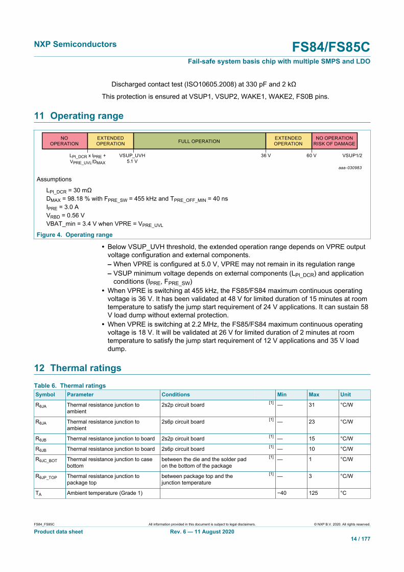
11 Operating range
aaa-030983
NOOPERATION
NO OPERATIONRISK OF DAMAGE
VSUP1/260 V
EXTENDEDOPERATION FULL OPERATION EXTENDED
OPERATION
36 VVSUP_UVH5.1 V
LPI_DCR x IPRE +VPRE_UVL/DMAX
Assumptions
LPI_DCR = 30 mΩDMAX = 98.18 % with FPRE_SW = 455 kHz and TPRE_OFF_MIN = 40 nsIPRE = 3.0 AVRBD = 0.56 VVBAT_min = 3.4 V when VPRE = VPRE_UVL
Figure 4. Operating range
• Below VSUP_UVH threshold, the extended operation range depends on VPRE outputvoltage configuration and external components.– When VPRE is configured at 5.0 V, VPRE may not remain in its regulation range– VSUP minimum voltage depends on external components (LPI_DCR) and application
conditions (IPRE, FPRE_SW)• When VPRE is switching at 455 kHz, the FS85/FS84 maximum continuous operating
voltage is 36 V. It has been validated at 48 V for limited duration of 15 minutes at roomtemperature to satisfy the jump start requirement of 24 V applications. It can sustain 58V load dump without external protection.
• When VPRE is switching at 2.2 MHz, the FS85/FS84 maximum continuous operatingvoltage is 18 V. It will be validated at 26 V for limited duration of 2 minutes at roomtemperature to satisfy the jump start requirement of 12 V applications and 35 V loaddump.
12 Thermal ratingsTable 6. Thermal ratingsSymbol Parameter Conditions Min Max Unit
RθJA Thermal resistance junction toambient
2s2p circuit board [1] — 31 °C/W
RθJA Thermal resistance junction toambient
2s6p circuit board [1] — 23 °C/W
RθJB Thermal resistance junction to board 2s2p circuit board [1] — 15 °C/W
RθJB Thermal resistance junction to board 2s6p circuit board [1] — 10 °C/W
RθJC_BOT Thermal resistance junction to casebottom
between the die and the solder padon the bottom of the package
[1] — 1 °C/W
RθJP_TOP Thermal resistance junction topackage top
between package top and thejunction temperature
[1] — 3 °C/W
TA Ambient temperature (Grade 1) −40 125 °C

NXP Semiconductors FS84/FS85CFail-safe system basis chip with multiple SMPS and LDO
FS84_FS85C All information provided in this document is subject to legal disclaimers. © NXP B.V. 2020. All rights reserved.
Product data sheet Rev. 6 — 11 August 202015 / 177
Symbol Parameter Conditions Min Max Unit
TJ Junction temperature (Grade 1) −40 150 °C
TSTG Storage temperature −55 150 °C
[1] per JEDEC JESD51-2 and JESD51-8
13 CharacteristicsTable 7. Electrical characteristicsTA = −40 °C to 125 °C, unless otherwise specified. VSUP = VSUP_UVH to 36 V, unless otherwise specified. All voltagesreferenced to ground.
Symbol Parameter Min Typ Max Unit
Power supply
ISUP_NORMAL Current in Normal mode, all regulators ON (IOUT = 0) — 15 25 mA
ISUP_STANDBYCurrent in Standby mode, all regulators OFF exceptVBOS — 5 10 mA
ISUP_OFF1 Current in OFF mode (Power Down), TA < 85 °C — 10 15 μA
ISUP_OFF2 Current in OFF mode (Power Down), TA = 125 °C — — 25 μA
VSUP_UV7 VSUP undervoltage threshold (7.0 V) 7.2 7.5 7.8 V
VSUP undervoltage threshold high (during power upand Vsup rising) OTP_VSUP_CFG = 0 4.7 — 5.1 V
VSUP_UVHVSUP undervoltage threshold high (during power upand Vsup rising) OTP_VSUP_CFG = 1 6.0 — 6.4 V
VSUP undervoltage threshold low (during power upand Vsup falling) OTP_VSUP_CFG = 0 4.0 — 4.4 V
VSUP_UVLVSUP undervoltage threshold low (during power upand Vsup falling) OTP_VSUP_CFG = 1 5.3 — 5.7 V
TSUP_UV VSUP_UV7, VSUP_UVH and VSUP_UVL filtering time 6.0 10 15 μs
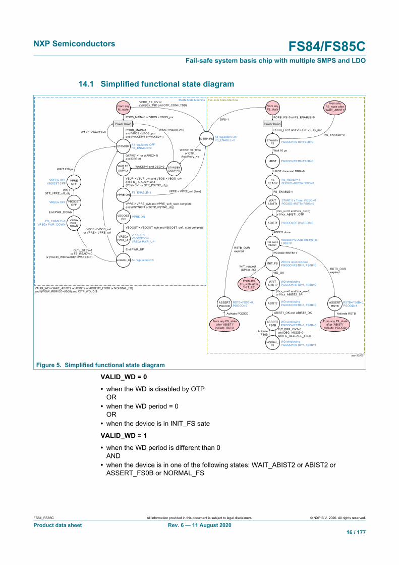
14 Functional description
The FS85/FS84 device has two independent logic blocks. The main state machinemanages the power management, the Standby mode and the wake-up sources. The fail-safe state machine manages the monitoring of the power management, the monitoring ofthe MCU and the monitoring of an external IC.
NXP Semiconductors FS84/FS85CFail-safe system basis chip with multiple SMPS and LDO
FS84_FS85C All information provided in this document is subject to legal disclaimers. © NXP B.V. 2020. All rights reserved.
Product data sheet Rev. 6 — 11 August 202016 / 177
14.1 Simplified functional state diagram
aaa-035671
From anyFS_state
From anyM_state
From anyFS_state after
`WAIT_ABIST1'
From any FS_stateafter ABIST1'
exclude `PGOOD'
PORB_FS=0 or FS_ENABLE=0
PORB_FS=1 and VBOS > VBOS_por
PGOOD=RSTB=FS0B=0
PGOOD=RSTB=FS0B=0
Release PGOOD and RSTBFS0B=0
256 ms open windowPGOOD=RSTB=1, FS0B=0
RSTB=FS0B=0,PGOOD=0
RSTB=FS0B=0,PGOOD=1
PGOOD=RSTB=FS0B=0
FS_READY=1PGOOD=RSTB=FS0B=0
START 8 s Timer if DBG=0PGOOD=RSTB=FS0B=0
Power Down
STANDBYFS
Wait 10 µs
FS_ENABLE=0
RSTB_DURexpired
RSTB_DURexpired
INIT_request(SPI or I2C)
LBIST
LBIST done and DBG=0
FSREADY
FS_ENABLE=1
WAITABIST1
(Vxx_uv=0 and Vxx_ov=0)or !Vxx_ABIST1_OTP
ABIST1
DEEP-FS
ABIST1 done
RELEASERESET
PGOOD=RSTB=1
INIT_FS
WD_OK
WAITABIST2
(Vxx_uv=0 and Vxx_ov=0)or !Vxx_ABIST2_SPI
ABIST2
ABIST1_OK and ABIST2_OK
ASSERTFS0B
ASSERTRSTB
FLT_ERR_CNT=0and DBG_MODE=0and FS_RELEASE_FS0B
WD windowingPGOOD=RSTB=1, FS0B=1
WD windowingPGOOD=RSTB=1, FS0B=0
WD windowingPGOOD=RSTB=1, FS0B=0
WD windowingPGOOD=RSTB=1, FS0B=0
ActivateFS0B
Activate RSTB
From any FS_stateafter ABIST1'include `RSTB'
ASSERTPGOOD
Activate PGOOD
NORMAL_FS
PORB_MAIN=0 or VBOS < VBOS_por
PORB_MAIN=1and VBOS >VBOS_porand (WAKE1=1 or WAKE2=1)
All regulators OFFFS_ENABLE=0
VPRE ONVBOOST ONVREGx PWR_UP
All regulators ON
VPRE > VPRE_uvh and VPRE_soft_start completeand (PSYNC=1 or !OTP_PSYNC_cfg)
VPRE ON
FS_ENABLE=1 VPRE < VPRE_uvl (2ms)
Power Down
STANDBY
(WAKE1=1 or WAKE2=1)and DBG=0
WAKE1=WAKE2=0
WAKE1=1 and DBG=0
WAKE1=0 (1ms)or OTP_
AutoRetry_4s
WAKE1=WAKE2=0
VPRE_FB_OV or(VREGx_TSD and OTP_CONF_TSD)
All regulators OFFFS_ENABLE=0
DFS=1
Fail-safe State MachineMAIN State Machine
WAIT FS&
SUPPLYSTANDBYDEEP-FS
VSUP > VSUP_uvh and VBOS > VBOS_uvhand FS_READY=1 and(PSYNC=1 or OTP_PSYNC_cfg)
VPRE ON
VBOOSTON
VBOOST > VBOOST_uvh and VBOOST_soft_start complete
VREGxPWR_UP
VALID_WD = WAIT_ABIST2 or ABIST2 or ASSERT_FSOB or NORMAL_FS)and !(WDW_PERIOD=0000) and !OTP_WD_DIS
VPREOFF
VBOOSTOFF
End PWR_DOWN
VREGx OFF
VREGx OFFVBOOST OFF
WAIT 250 µs
FS_ENABLE=0VREGx PWR_DOWN
GoTo_STBY=1or FS_READY=0
or (VALID_WD=WAKE1=WAKE2=0)
VBOS < VBOS_uvlor VPRE < VPRE_uvl
WAITOTP_VPRE_off_dly
VREGxPWR_DOWN
End PWR_UP
NORMAL_M
From anyFS_state after
INIT_FS'
Figure 5. Simplified functional state diagram
VALID_WD = 0
• when the WD is disabled by OTPOR
• when the WD period = 0OR
• when the device is in INIT_FS sate
VALID_WD = 1
• when the WD period is different than 0AND
• when the device is in one of the following states: WAIT_ABIST2 or ABIST2 orASSERT_FS0B or NORMAL_FS

NXP Semiconductors FS84/FS85CFail-safe system basis chip with multiple SMPS and LDO
FS84_FS85C All information provided in this document is subject to legal disclaimers. © NXP B.V. 2020. All rights reserved.
Product data sheet Rev. 6 — 11 August 202017 / 177
14.2 Main state machineThe FS85/FS84 starts when VSUP > VSUP_UVH and WAKE1 or WAKE2 > WAKE12VIHwith VBOS first, followed by VPRE, VBOOST and the power up sequencing from theOTP programming for the remaining regulators if PSYNC pin is pulled up to VBOS. Ifduring the power up sequence VSUP < VSUP_UVL, the device goes back to Standbymode. When the power up is finished, the main state machine is in Normal_M modewhich is the application running mode with all the regulators ON and VSUP_UVL has noeffect even if VSUP < VSUP_UVL. See Figure 4 for the minimum operating voltage.
The power up sequence can be synchronized with another PMIC using the PSYNC pinin order to stop before or after VPRE is ON and wait for the PMIC feedback on PSYNCpin before allowing FS85/FS84 to continue its power up sequence. See Section 27.3"PSYNC for two FS85" for more details on PSYNC pin. If the power up sequence fromVPRE ON to NORMAL_M is not completed within 1 second, the device goes backto Standby mode. VPRE restarts when VSUP > VSUP_UVH and WAKE1 or WAKE2 >WAKE12VIH.
The device goes to Standby mode by a SPI/I2C command from the MCU. If the WDis disabled by OTP_WD_DIS bit, for an application without MCU, the device goes toStandby mode when both WAKE1 and WAKE 2 = 0. The device goes to Standby modefollowing the power down sequence to stop all the regulators in the reverse order ofthe power up sequence. VPRE shutdown can be delayed from 250 μs to 32 ms byOTP_VPRE_off_dly bit in case VPRE is supplying an external PMIC to wait its powerdown sequence completion.
In case of loss of VPRE (VPRE < VPRE_UVL) or loss of VBOS (VBOS < VBOS_UVL), thedevice stops and goes directly to Standby mode without power down sequence. VPRErestarts when VSUP > VSUP_UVH and WAKE1 or WAKE2 > WAKE12VIH.
In case of VPRE_FB_OV detection, or TSD detection on a regulator depending onOTP_conf_tsd[5:0] bits configuration, or deep fail-safe request from the fail-safe statemachine when DFS = 1, the device stops and goes directly to DEEP-FS mode withoutpower down sequence.
Exit of DEEP-FS mode is only possible by WAKE1 = 0 or after 4 s if the autoretry featureis activated by OTP_Autorety_en bit. The number of autroretry can be limited to 15 orinfinite depending on OTP_Autoretry_infinite bit. VPRE restarts when VSUP > VSUP_UVHand WAKE1 > WAKE12VIH.
14.3 Fail-safe state machineThe fail-safe state machine starts with LBIST execution when VBOS > VBOS_POR. Whenthe LBIST is done, the 8 s timer monitoring the RSTB pin starts and the ABIST1 isautomatically executed when all the regulators assigned to ABIST1 have passed theirundervoltage threshold and remain under their overvoltage threshold. When the ABIST1is done, RSTB and PGOOD pins are released and the initialization of the device isopened for 256 ms. If the WD is not correctly refreshed within the 256 ms window, RSTBis asserted and the fault error counter is increased by 1. ABIST1 fail does not preventRSTB and PGOOD release but maintains FS0B asserted.
The first good watchdog refresh closes the INIT_FS. Continuous watchdogrefresh is now required. The device waits for the regulators assigned to ABIST2 inFS_I_OVUV_SAFE_REACTION1 register during INIT_FS to be started. When theABIST2 is done and pass, the fault counter must be cleared with the appropriate number

NXP Semiconductors FS84/FS85CFail-safe system basis chip with multiple SMPS and LDO
FS84_FS85C All information provided in this document is subject to legal disclaimers. © NXP B.V. 2020. All rights reserved.
Product data sheet Rev. 6 — 11 August 202018 / 177
of good watchdog refresh to release the FS0B pin per the procedure described inSection 32.9.4 "FS0B release".
When FS0B pin is released, the device is ready for application running mode with allthe selected monitoring activated. From now on, the FS85/FS84 reacts by asserting thesafety pins (PGOOD, RSTB and FS0B) according to its configuration when a fault isdetected. The safety pins hierarchical priority is 1-PGOOD, 2-RSTB, 3-FS0B.
14.4 Power sequencingVPRE is the first regulator to start automatically, followed by the BOOST, before theSLOT_0. The other regulators are starting from the OTP power sequencing configuration.Seven slots are available to program the start-up sequence of BUCK1, BUCK 2, BUCK 3,LDO1 and LDO2 regulators. The delay between each slot is configurable to 250 µs or 1ms by OTP using OTP_Tslot bit to accommodate the different ramp up speed of BUCK1,BUCK2 and BUCK3.
The power up sequence starts at SLOT_0 and ends at SLOT_7 while the power downsequence is executed in reverse order. This means that all regulators set to SLOT_7 andpowered up by SPI/I2C, will be stopped first during the power down sequence. All theSLOTs are executed even if there is no regulator assigned to a SLOT. The regulatorsassigned to SLOT_7 are not started during the power up sequence. They can be started(or not) later in NORMAL_M mode with a SPI/I2C command to write in M_REG_CTRL1register if they were enabled by OTP.
aaa-035669
FromVBOOST ON
VBOOST > VBOOST_uvhand VBOOST_soft_start complete
SLOT_0
ToNORMAL_M
tslot
SLOT_1
tslot
SLOT_2
tslot
SLOT_3
tslot
SLOT_4
tslot
SLOT_5
tslot
SLOT_6
tslot
Figure 6. Power sequencing (VREGx PWR_UP)
Each regulator is assigned to a SLOT by OTP configuration using OTP_VB1S[2:0] forBUCK1, OTP_VB2S[2:0] for BUCK2, OTP_VB3S[2:0] for BUCK3, OTP_LDO1S[2:0] forLDO1 and OTP_LDO2S[2:0] for LDO2.

NXP Semiconductors FS84/FS85CFail-safe system basis chip with multiple SMPS and LDO
FS84_FS85C All information provided in this document is subject to legal disclaimers. © NXP B.V. 2020. All rights reserved.
Product data sheet Rev. 6 — 11 August 202019 / 177
The different soft start duration of the BUCKs and the LDOs should be considered in theSLOT assignment to achieve the correct sequence.
aaa-035667
VSUP1,2
VSUP > VSUP_uvh
WAKE12VIH
VBOS_uvh
VPRE_uvh andVPRE_soft_start complete
VBOOST_uvh andVBOOST_Soft_start complete
VPRE - VBOOST_diode
Tslot
Tslot
WAKE1or WAKE2
VBOS
VPRE
VBOOST
SLOT_0
SLOT_1
SLOT_2
SLOT_6
PGOOD
RSTB
Figure 7. Power up sequence example
PGOOD and RSTB release depends on the combination of the power up sequenceand what regulator is assigned to PGOOD and ABIST1 through the voltage monitoringconnection (VCOREMON, VDDIOMON and VMONx). The FS85_FS84_OTP_Config fileused to generate the OTP configuration of the device draws the power up sequence ofan OTP configuration in the OTP_conf_summary sheet.
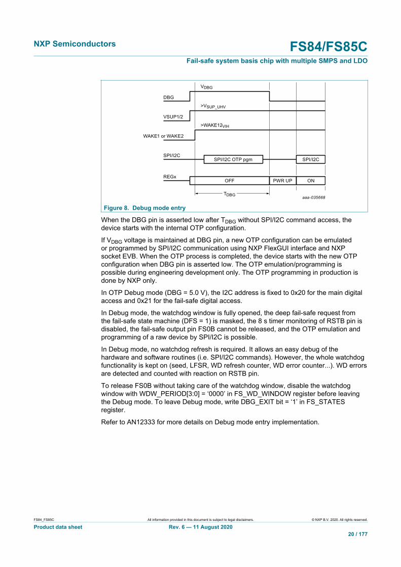
14.5 Debug modeThe FS85/FS84 enters in Debug mode with the sequence described in Figure 8:
1. DBG pin = VDBG and VSUP > VSUP_UVH2. WAKE1 or WAKE2 > WAKE12VIH
VDBG and VSUP can come up at the same time as long as WAKE1 or WAKE2 comes upthe last.
NXP Semiconductors FS84/FS85CFail-safe system basis chip with multiple SMPS and LDO
FS84_FS85C All information provided in this document is subject to legal disclaimers. © NXP B.V. 2020. All rights reserved.
Product data sheet Rev. 6 — 11 August 202020 / 177
aaa-035668
DBG
VDBG
SPI/I2C OTP pgm SPI/I2C
VSUP1/2
>VSUP_UHV
WAKE1 or WAKE2
>WAKE12VIH
SPI/I2C
OFF
TDBG
ONREGx
PWR UP
Figure 8. Debug mode entry
When the DBG pin is asserted low after TDBG without SPI/I2C command access, thedevice starts with the internal OTP configuration.
If VDBG voltage is maintained at DBG pin, a new OTP configuration can be emulatedor programmed by SPI/I2C communication using NXP FlexGUI interface and NXPsocket EVB. When the OTP process is completed, the device starts with the new OTPconfiguration when DBG pin is asserted low. The OTP emulation/programming ispossible during engineering development only. The OTP programming in production isdone by NXP only.
In OTP Debug mode (DBG = 5.0 V), the I2C address is fixed to 0x20 for the main digitalaccess and 0x21 for the fail-safe digital access.
In Debug mode, the watchdog window is fully opened, the deep fail-safe request fromthe fail-safe state machine (DFS = 1) is masked, the 8 s timer monitoring of RSTB pin isdisabled, the fail-safe output pin FS0B cannot be released, and the OTP emulation andprogramming of a raw device by SPI/I2C is possible.
In Debug mode, no watchdog refresh is required. It allows an easy debug of thehardware and software routines (i.e. SPI/I2C commands). However, the whole watchdogfunctionality is kept on (seed, LFSR, WD refresh counter, WD error counter...). WD errorsare detected and counted with reaction on RSTB pin.
To release FS0B without taking care of the watchdog window, disable the watchdogwindow with WDW_PERIOD[3:0] = ‘0000’ in FS_WD_WINDOW register before leavingthe Debug mode. To leave Debug mode, write DBG_EXIT bit = ‘1’ in FS_STATESregister.
Refer to AN12333 for more details on Debug mode entry implementation.

NXP Semiconductors FS84/FS85CFail-safe system basis chip with multiple SMPS and LDO
FS84_FS85C All information provided in this document is subject to legal disclaimers. © NXP B.V. 2020. All rights reserved.
Product data sheet Rev. 6 — 11 August 202021 / 177
Table 8. Electrical characteristicsTA = −40 °C to 125 °C, unless otherwise specified. VSUP = VSUP_UVH to 36 V, unless otherwisespecified. All voltages referenced to ground.
Symbol Parameter Min Typ Max Unit
VDBG Debug mode entry threshold 4.5 5 5.5 V
TDBG
Debug mode entry filtering time(minimum duration of DBG = VDBG afterVSUP > VSUP_UVH and WAKE1 or WAKE2 >WAKE12VIH
7 — — ms
14.6 Flow chartsThe flow charts describe how the device starts and what to do when the RSTB pin isreleased.
14.6.1 Application flow chart
In application mode, the Debug pin is connected to GND and watchdog refresh isrequired as soon as INIT_FS is closed.

NXP Semiconductors FS84/FS85CFail-safe system basis chip with multiple SMPS and LDO
FS84_FS85C All information provided in this document is subject to legal disclaimers. © NXP B.V. 2020. All rights reserved.
Product data sheet Rev. 6 — 11 August 202022 / 177
aaa-031034
ABIST2 fail prevent the release of FS0B pinPossibility to go back to INIT_FS by SPI/I2C
and remove the failing regulator fromABIST2 list
LBIST fail prevent the release of FS0B pinABIST1 fail prevent the release of FS0B pin
Possibility to go back to STANDBYby SPI/I2C and restart the device
RSTB release
INIT
_FS
win
dow
is25
6m
sm
axW
Dre
fres
hre
quire
dLBIST_OK == 1
No
Yes
Write all INIT_FS registersWith Reg/Reg_NOT procedure
Assign Vregx to ABIST2Configure SVS if needed
Close INIT_FSwith 1x good WD refresh
STANDBY
NoABIST1_OK == 1
Yes
Wait Vregx pwr up
Launch ABIST2 by SPI/I2C
Wait 1.2 ms
Decrease FLT_ERR_CNT to 0'with WD_ERR_LIMIT
good WD refresh
NoABIST2_OK == 1
Yes
Release FS0B withRELEASE_FS0B[23:8]=NOT_WD_SEED[8:23]
Figure 9. Application flow chart
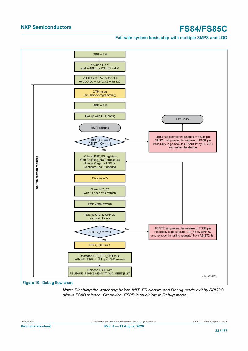
14.6.2 Debug flow chart
In Debug mode, the Debug pin is managed according to Section 14.4 "Powersequencing" description. The watchdog window is fully opened, and the watchdog refreshis not required.
NXP Semiconductors FS84/FS85CFail-safe system basis chip with multiple SMPS and LDO
FS84_FS85C All information provided in this document is subject to legal disclaimers. © NXP B.V. 2020. All rights reserved.
Product data sheet Rev. 6 — 11 August 202023 / 177
aaa-035678
RSTB release
Write all INIT_FS registersWith Reg/Reg_NOT procedure
Assign Vregx to ABIST2Configure SVS if needed
LBIST fail prevent the release of FS0B pinABIST1 fail prevent the release of FS0B pin
Possibility to go back to STANDBY by SPI/I2Cand restart the device
STANDBY
NO
WD
refr
esh
requ
ired
DBG = 5 V
VSUP > 6.5 Vand WAKE1 or WAKE2 > 4 V
VDDIO = 3.3 V/5 V for SPIor VDDI2C = 1.8 V/3.3 V for I2C
OTP mode(emulation/programming)
Pwr up with OTP config
DBG = 0 V
Close INIT_FSwith 1x good WD refresh
Decrease FLT_ERR_CNT to 0'with WD_ERR_LIMIT good WD refresh
Wait Vregx pwr up
Run ABIST2 by SPI/I2Cand wait 1.2 ms
Release FS0B withRELEASE_FS0B[23:8]=NOT_WD_SEED[8:23]
Disable WD
DBG_EXIT == 1
ABIST2 fail prevent the release of FS0B pinPossibility to go back to INIT_FS by SPI/I2C
and remove the failing regulator from ABIST2 list
NoLBIST_OK == 1ABIST1_OK == 1
Yes
NoABIST2_OK == 1
Yes
Figure 10. Debug flow chart
Note: Disabling the watchdog before INIT_FS closure and Debug mode exit by SPI/I2Callows FS0B release. Otherwise, FS0B is stuck low in Debug mode.
NXP Semiconductors FS84/FS85CFail-safe system basis chip with multiple SMPS and LDO
FS84_FS85C All information provided in this document is subject to legal disclaimers. © NXP B.V. 2020. All rights reserved.
Product data sheet Rev. 6 — 11 August 202024 / 177
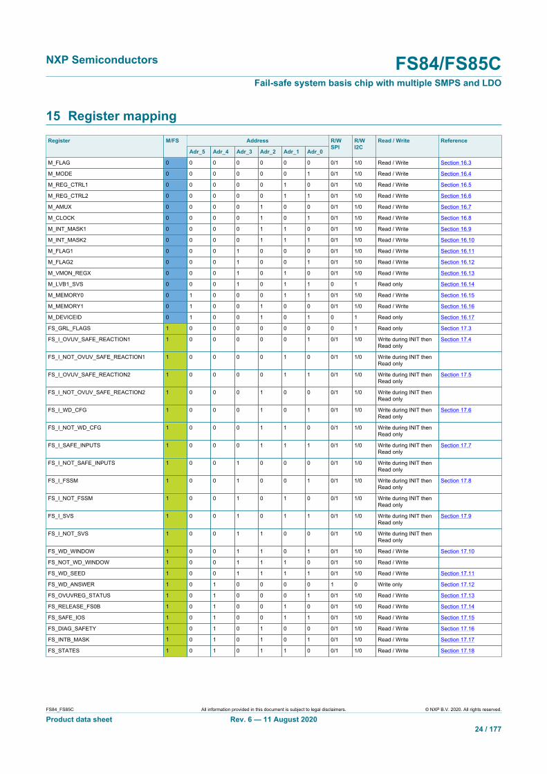
15 Register mappingAddressRegister M/FS
Adr_5 Adr_4 Adr_3 Adr_2 Adr_1 Adr_0
R/WSPI
R/WI2C
Read / Write Reference
M_FLAG 0 0 0 0 0 0 0 0/1 1/0 Read / Write Section 16.3
M_MODE 0 0 0 0 0 0 1 0/1 1/0 Read / Write Section 16.4
M_REG_CTRL1 0 0 0 0 0 1 0 0/1 1/0 Read / Write Section 16.5
M_REG_CTRL2 0 0 0 0 0 1 1 0/1 1/0 Read / Write Section 16.6
M_AMUX 0 0 0 0 1 0 0 0/1 1/0 Read / Write Section 16.7
M_CLOCK 0 0 0 0 1 0 1 0/1 1/0 Read / Write Section 16.8
M_INT_MASK1 0 0 0 0 1 1 0 0/1 1/0 Read / Write Section 16.9
M_INT_MASK2 0 0 0 0 1 1 1 0/1 1/0 Read / Write Section 16.10
M_FLAG1 0 0 0 1 0 0 0 0/1 1/0 Read / Write Section 16.11
M_FLAG2 0 0 0 1 0 0 1 0/1 1/0 Read / Write Section 16.12
M_VMON_REGX 0 0 0 1 0 1 0 0/1 1/0 Read / Write Section 16.13
M_LVB1_SVS 0 0 0 1 0 1 1 0 1 Read only Section 16.14
M_MEMORY0 0 1 0 0 0 1 1 0/1 1/0 Read / Write Section 16.15
M_MEMORY1 0 1 0 0 1 0 0 0/1 1/0 Read / Write Section 16.16
M_DEVICEID 0 1 0 0 1 0 1 0 1 Read only Section 16.17
FS_GRL_FLAGS 1 0 0 0 0 0 0 0 1 Read only Section 17.3
FS_I_OVUV_SAFE_REACTION1 1 0 0 0 0 0 1 0/1 1/0 Write during INIT thenRead only
Section 17.4
FS_I_NOT_OVUV_SAFE_REACTION1 1 0 0 0 0 1 0 0/1 1/0 Write during INIT thenRead only
FS_I_OVUV_SAFE_REACTION2 1 0 0 0 0 1 1 0/1 1/0 Write during INIT thenRead only
Section 17.5
FS_I_NOT_OVUV_SAFE_REACTION2 1 0 0 0 1 0 0 0/1 1/0 Write during INIT thenRead only
FS_I_WD_CFG 1 0 0 0 1 0 1 0/1 1/0 Write during INIT thenRead only
Section 17.6
FS_I_NOT_WD_CFG 1 0 0 0 1 1 0 0/1 1/0 Write during INIT thenRead only
FS_I_SAFE_INPUTS 1 0 0 0 1 1 1 0/1 1/0 Write during INIT thenRead only
Section 17.7
FS_I_NOT_SAFE_INPUTS 1 0 0 1 0 0 0 0/1 1/0 Write during INIT thenRead only
FS_I_FSSM 1 0 0 1 0 0 1 0/1 1/0 Write during INIT thenRead only
Section 17.8
FS_I_NOT_FSSM 1 0 0 1 0 1 0 0/1 1/0 Write during INIT thenRead only
FS_I_SVS 1 0 0 1 0 1 1 0/1 1/0 Write during INIT thenRead only
Section 17.9
FS_I_NOT_SVS 1 0 0 1 1 0 0 0/1 1/0 Write during INIT thenRead only
FS_WD_WINDOW 1 0 0 1 1 0 1 0/1 1/0 Read / Write Section 17.10
FS_NOT_WD_WINDOW 1 0 0 1 1 1 0 0/1 1/0 Read / Write
FS_WD_SEED 1 0 0 1 1 1 1 0/1 1/0 Read / Write Section 17.11
FS_WD_ANSWER 1 0 1 0 0 0 0 1 0 Write only Section 17.12
FS_OVUVREG_STATUS 1 0 1 0 0 0 1 0/1 1/0 Read / Write Section 17.13
FS_RELEASE_FS0B 1 0 1 0 0 1 0 0/1 1/0 Read / Write Section 17.14
FS_SAFE_IOS 1 0 1 0 0 1 1 0/1 1/0 Read / Write Section 17.15
FS_DIAG_SAFETY 1 0 1 0 1 0 0 0/1 1/0 Read / Write Section 17.16
FS_INTB_MASK 1 0 1 0 1 0 1 0/1 1/0 Read / Write Section 17.17
FS_STATES 1 0 1 0 1 1 0 0/1 1/0 Read / Write Section 17.18

NXP Semiconductors FS84/FS85CFail-safe system basis chip with multiple SMPS and LDO
FS84_FS85C All information provided in this document is subject to legal disclaimers. © NXP B.V. 2020. All rights reserved.
Product data sheet Rev. 6 — 11 August 202025 / 177
16 Main register mapping
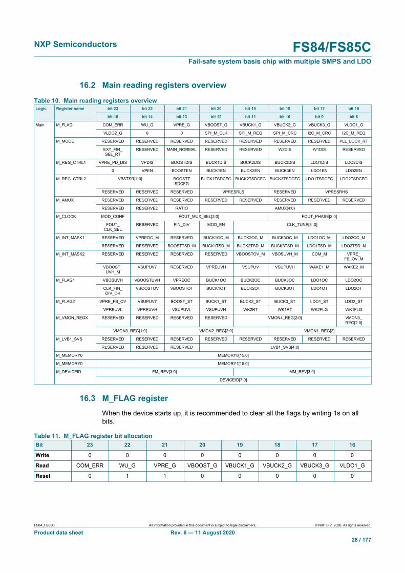
16.1 Main writing registers overview
Table 9. Main writing registers overviewbit 23 bit 22 bit 21 bit 20 bit 19 bit 18 bit 17 bit 16Logic Register name
bit 15 bit 14 bit 13 bit 12 bit 11 bit 10 bit 9 bit 8
0 0 0 0 0 0 0 0M_FLAG
0 0 0 SPI_M_CLK SPI_M_REQ SPI_M_CRC I2C_M_CRC I2C_M_REQ
0 0 0 0 0 0 0 0M_MODE
0 EXT_FIN_DIS 0 0 0 W2DIS W1DIS GoTo_STBY
VPRE_PD_DIS VPDIS BOOSTDIS BUCK1DIS BUCK2DIS BUCK3DIS LDO1DIS LDO2DISM_REG_CTRL1
0 VPEN BOOSTEN BUCK1EN BUCK2EN BUCK3EN LDO1EN LDO2EN
VBSTSR[1:0] BOOSTTSDCFG
BUCK1TSDCFG BUCK2TSDCFG BUCK3TSDCFG LDO1TSDCFG LDO2TSDCFGM_REG_CTRL2
0 0 0 VPRESRLS 0 VPRESRHS
0 0 0 0 0 0 0 0M_AMUX
0 0 RATIO AMUX[4:0)
MOD_CONF FOUT_MUX_SEL[3:0] FOUT_PHASE[2:0]M_CLOCK
FOUT_CLK_SEL
EXT_FIN_SEL FIN_DIV MOD_EN CLK_TUNE[3 :0]
0 VPREOC_M 0 BUCK1OC_M BUCK2OC_M BUCK3OC_M LDO1OC_M LDO2OC_MM_INT_MASK1
0 0 BOOSTTSD_M BUCK1TSD_M BUCK2TSD_M BUCK3TSD_M LDO1TSD_M LDO2TSD_M
0 0 0 0 VBOOSTOV_M VBOSUVH_M COM_M VPRE_FB_OV_M
M_INT_MASK2
VBOOST_UVH_M
VSUPUV7 0 VPREUVH VSUPUV VSUPUVH WAKE1_M WAKE2_M
VBOSUVH VBOOSTUVH VPREOC BUCK1OC BUCK2OC BUCK3OC LDO1OC LDO2OCM_FLAG1
0 VBOOSTOV VBOOSTOT BUCK1OT BUCK2OT BUCK3OT LDO1OT LDO2OT
VPRE_FB_OV VSUPUV7 0 0 0 0 0 0M_FLAG2
VPREUVL VPREUVH VSUPUVL VSUPUVH 0 0 WK2FLG WK1FLG
0 0 0 0 VMON4_REG[2:0] VMON3_REG[2:0]
M_VMON_REGX
VMON3_REG[1:0] VMON2_REG[2:0] VMON1_REG[2]
M_MEMORY0 MEMORY0[15:0]
Main
M_MEMORY1 MEMORY1[15:0]
NXP Semiconductors FS84/FS85CFail-safe system basis chip with multiple SMPS and LDO
FS84_FS85C All information provided in this document is subject to legal disclaimers. © NXP B.V. 2020. All rights reserved.
Product data sheet Rev. 6 — 11 August 202026 / 177
16.2 Main reading registers overview
Table 10. Main reading registers overviewbit 23 bit 22 bit 21 bit 20 bit 19 bit 18 bit 17 bit 16Logic Register name
bit 15 bit 14 bit 13 bit 12 bit 11 bit 10 bit 9 bit 8
COM_ERR WU_G VPRE_G VBOOST_G VBUCK1_G VBUCK2_G VBUCK3_G VLDO1_GM_FLAG
VLDO2_G 0 0 SPI_M_CLK SPI_M_REQ SPI_M_CRC I2C_M_CRC I2C_M_REQ
RESERVED RESERVED RESERVED RESERVED RESERVED RESERVED RESERVED PLL_LOCK_RTM_MODE
EXT_FIN_SEL_RT
RESERVED MAIN_NORMAL RESERVED RESERVED W2DIS W1DIS RESERVED
VPRE_PD_DIS VPDIS BOOSTDIS BUCK1DIS BUCK2DIS BUCK3DIS LDO1DIS LDO2DISM_REG_CTRL1
0 VPEN BOOSTEN BUCK1EN BUCK2EN BUCK3EN LDO1EN LDO2EN
VBSTSR[1:0] BOOSTTSDCFG
BUCK1TSDCFG BUCK2TSDCFG BUCK3TSDCFG LDO1TSDCFG LDO2TSDCFGM_REG_CTRL2
RESERVED RESERVED RESERVED VPRESRLS RESERVED VPRESRHS
RESERVED RESERVED RESERVED RESERVED RESERVED RESERVED RESERVED RESERVEDM_AMUX
RESERVED RESERVED RATIO AMUX[4:0)
MOD_CONF FOUT_MUX_SEL[3:0] FOUT_PHASE[2:0]M_CLOCK
FOUT_CLK_SEL
RESERVED FIN_DIV MOD_EN CLK_TUNE[3 :0]
RESERVED VPREOC_M RESERVED BUCK1OC_M BUCK2OC_M BUCK3OC_M LDO1OC_M LDO2OC_MM_INT_MASK1
RESERVED RESERVED BOOSTTSD_M BUCK1TSD_M BUCK2TSD_M BUCK3TSD_M LDO1TSD_M LDO2TSD_M
RESERVED RESERVED RESERVED RESERVED VBOOSTOV_M VBOSUVH_M COM_M VPRE_FB_OV_M
M_INT_MASK2
VBOOST_UVH_M
VSUPUV7 RESERVED VPREUVH VSUPUV VSUPUVH WAKE1_M WAKE2_M
VBOSUVH VBOOSTUVH VPREOC BUCK1OC BUCK2OC BUCK3OC LDO1OC LDO2OCM_FLAG1
CLK_FIN_DIV_OK
VBOOSTOV VBOOSTOT BUCK1OT BUCK2OT BUCK3OT LDO1OT LDO2OT
VPRE_FB_OV VSUPUV7 BOOST_ST BUCK1_ST BUCK2_ST BUCK3_ST LDO1_ST LDO2_STM_FLAG2
VPREUVL VPREUVH VSUPUVL VSUPUVH WK2RT WK1RT WK2FLG WK1FLG
RESERVED RESERVED RESERVED RESERVED VMON4_REG[2:0] VMON3_REG[2:0]
M_VMON_REGX
VMON3_REG[1:0] VMON2_REG[2:0] VMON1_REG[2]
RESERVED RESERVED RESERVED RESERVED RESERVED RESERVED RESERVED RESERVEDM_LVB1_SVS
RESERVED RESERVED RESERVED LVB1_SVS[4:0]
M_MEMORY0 MEMORY0[15:0]
M_MEMORY0 MEMORY1[15:0]
FM_REV[3:0] MM_REV[3:0]
Main
M_DEVICEID
DEVICEID[7:0]
16.3 M_FLAG registerWhen the device starts up, it is recommended to clear all the flags by writing 1s on allbits.
Table 11. M_FLAG register bit allocationBit 23 22 21 20 19 18 17 16
Write 0 0 0 0 0 0 0 0
Read COM_ERR WU_G VPRE_G VBOOST_G VBUCK1_G VBUCK2_G VBUCK3_G VLDO1_G
Reset 0 1 1 0 0 0 0 0

NXP Semiconductors FS84/FS85CFail-safe system basis chip with multiple SMPS and LDO
FS84_FS85C All information provided in this document is subject to legal disclaimers. © NXP B.V. 2020. All rights reserved.
Product data sheet Rev. 6 — 11 August 202027 / 177
Bit 15 14 13 12 11 10 9 8
Write 0 0 0 SPI_M_CLK SPI_M_REQ SPI_M_CRC I2C_M_CRC I2C_M_REQ
Read VLDO2_G 0 0 SPI_M_CLK SPI_M_REQ SPI_M_CRC I2C_M_CRC I2C_M_REQ
Reset 0 0 0 0 0 0 0 0
Table 12. M_FLAG register bit descriptionBit Symbol Description
Report an error in the Communication (SPI or I2C)COM_ERR = SPI_M_CRC or SPI_M_CLK or SPI_M_REQ or I2C_M_CRC or I2C_M_REQ orFS_COM_G
0 No failure
1 Failure
23 COM_ERR
Reset condition: Real time information - cleared when all individual bits are cleared
Report a wake-up event by WAKE1 or WAKE2WU_G = WK1FLG or WK2FLG
0 No wake event
1 Wake event
22 WU_G
Reset condition: Real time information - cleared when all individual bits are cleared
Report an event on VPRE (status change or failure)VPRE_G = VPREOC or VPREUVH or VPREUVL or VPRE_FB_OV
0 No event
1 Event occurred
21 VPRE_G
Reset condition: Real time information - cleared when all individual bits are cleared
Report an event on VBOOST (status change or failure)VBOOST_G = VBOOSTOT or BOOSTOV
0 No event
1 Event occurred
20 VBOOST_G
Reset condition: Real time information - cleared when all individual bits are cleared
Report an event on BUCK1 (status change or failure)VBUCK1_G = BUCK1OC or BUCK1OT
0 No event
1 Event occurred
19 VBUCK1_G
Reset condition: Real time information - cleared when all individual bits are cleared
Report an event on BUCK2 (status change or failure)VBUCK2_G = BUCK2OC or BUCK2OT
0 No event
1 Event occurred
18 VBUCK2_G
Reset condition: Real time information - cleared when all individual bits are cleared
Report an event on BUCK3 (status change or failure)VBUCK3_G = BUCK3OC or BUCK3OT
0 No event
1 Event occurred
17 VBUCK3_G
Reset condition: Real time information - cleared when all individual bits are cleared

NXP Semiconductors FS84/FS85CFail-safe system basis chip with multiple SMPS and LDO
FS84_FS85C All information provided in this document is subject to legal disclaimers. © NXP B.V. 2020. All rights reserved.
Product data sheet Rev. 6 — 11 August 202028 / 177
Bit Symbol Description
Report an event on LDO1 (status change or failure)VLDO1_G = LDO1OC or LDO1OT
0 No event
1 Event occurred
16 VLDO1_G
Reset condition: Real time information
Report an event on LDO2 (status change or failure)VLDO2_G = LDO2OC or LDO2OT
0 No event
1 Event occurred
15 VLDO2_G
Reset condition: Real time information
Main domain SPI SCLK error detection
0 No error
1 Wrong number of clock cycles (<32 or >32)
12 SPI_M_CLK
Reset condition: POR / clear on Write (write ‘1’)
Invalid main domain SPI access (wrong Write or Read, Write to INIT registers in normal mode,wrong address)
0 No error
1 SPI violation
11 SPI_M_REQ
Reset condition: POR / clear on Write (write ‘1’)
Main domain SPI communication CRC issue
0 No error
1 Error detected in the SPI CRC
10 SPI_M_CRC
Reset condition: POR / clear on Write (write ‘1’)
Main domain I2C communication CRC issue
0 No error
1 Error detected in the I2C CRC
9 I2C_M_CRC
Reset condition: POR / clear on write (write ‘1’)
Invalid main domain I2C access (wrong Write or Read, Write to INIT registers in normal mode,wrong address)
0 No error
1 I2C violation
8 I2C_M_REQ
Reset condition: POR / clear on Write (write ‘1’)
16.4 M_MODE register
Table 13. M_MODE register bit allocationBit 23 22 21 20 19 18 17 16
Write 0 0 0 0 0 0 0 0
Read RESERVED RESERVED RESERVED RESERVED RESERVED RESERVED RESERVED PLL_LOCK_RT
Reset 0 0 0 0 0 0 0 0
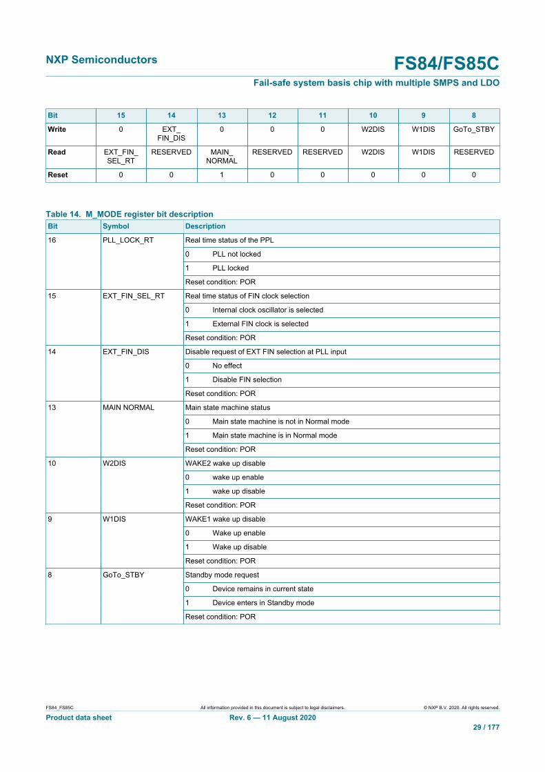
NXP Semiconductors FS84/FS85CFail-safe system basis chip with multiple SMPS and LDO
FS84_FS85C All information provided in this document is subject to legal disclaimers. © NXP B.V. 2020. All rights reserved.
Product data sheet Rev. 6 — 11 August 202029 / 177
Bit 15 14 13 12 11 10 9 8
Write 0 EXT_FIN_DIS
0 0 0 W2DIS W1DIS GoTo_STBY
Read EXT_FIN_SEL_RT
RESERVED MAIN_NORMAL
RESERVED RESERVED W2DIS W1DIS RESERVED
Reset 0 0 1 0 0 0 0 0
Table 14. M_MODE register bit descriptionBit Symbol Description
Real time status of the PPL
0 PLL not locked
1 PLL locked
16 PLL_LOCK_RT
Reset condition: POR
Real time status of FIN clock selection
0 Internal clock oscillator is selected
1 External FIN clock is selected
15 EXT_FIN_SEL_RT
Reset condition: POR
Disable request of EXT FIN selection at PLL input
0 No effect
1 Disable FIN selection
14 EXT_FIN_DIS
Reset condition: POR
Main state machine status
0 Main state machine is not in Normal mode
1 Main state machine is in Normal mode
13 MAIN NORMAL
Reset condition: POR
WAKE2 wake up disable
0 wake up enable
1 wake up disable
10 W2DIS
Reset condition: POR
WAKE1 wake up disable
0 Wake up enable
1 Wake up disable
9 W1DIS
Reset condition: POR
Standby mode request
0 Device remains in current state
1 Device enters in Standby mode
8 GoTo_STBY
Reset condition: POR

NXP Semiconductors FS84/FS85CFail-safe system basis chip with multiple SMPS and LDO
FS84_FS85C All information provided in this document is subject to legal disclaimers. © NXP B.V. 2020. All rights reserved.
Product data sheet Rev. 6 — 11 August 202030 / 177
16.5 M_REG_CTRL1 register
Table 15. M_REG_CTRL1 register bit allocationBit 23 22 21 20 19 18 17 16
Write VPRE_PD_DIS
VPDIS BOOSTDIS BUCK1DIS BUCK2DIS BUCK3DIS LDO1DIS LDO2DIS
Read VPRE_PD_DIS
RESERVED RESERVED RESERVED RESERVED RESERVED RESERVED RESERVED
Reset 0 0 0 0 0 0 0 0
Bit 15 14 13 12 11 10 9 8
Write 0 VPEN BOOSTEN BUCK1EN BUCK2EN BUCK3EN LDO1EN LDO2EN
Read RESERVED RESERVED RESERVED RESERVED RESERVED RESERVED RESERVED RESERVED
Reset 0 0 0 0 0 0 0 0
Table 16. M_REG_CTRL1 register bit descriptionBit Symbol Description
Force disable of VPRE pull down
0 No effect (VPRE pull down is automatically controlled by the logic)
1 VPRE pull down disable request
23 VPRE_PD_DIS
Reset condition: POR
Disable request of VPRE
0 No effect (regulator remains in existing state)
1 VPRE disable request
22 VPDIS
Reset condition: POR
Disable request of BOOST
0 No effect (regulator remains in existing state)
1 BOOST disable request
21 BOOSTDIS
Reset condition: POR
Disable request of BUCK1
0 No effect (regulator remains in existing state)
1 BUCK1 disable request
20 BUCK1DIS
Reset condition: POR
Disable request of BUCK2
0 No effect (regulator remains in existing state)
1 BUCK2 disable request
19 BUCK2DIS
Reset condition: POR
Disable request of BUCK3
0 No effect (regulator remains in existing state)
1 BUCK3 disable request
18 BUCK3DIS
Reset condition: POR
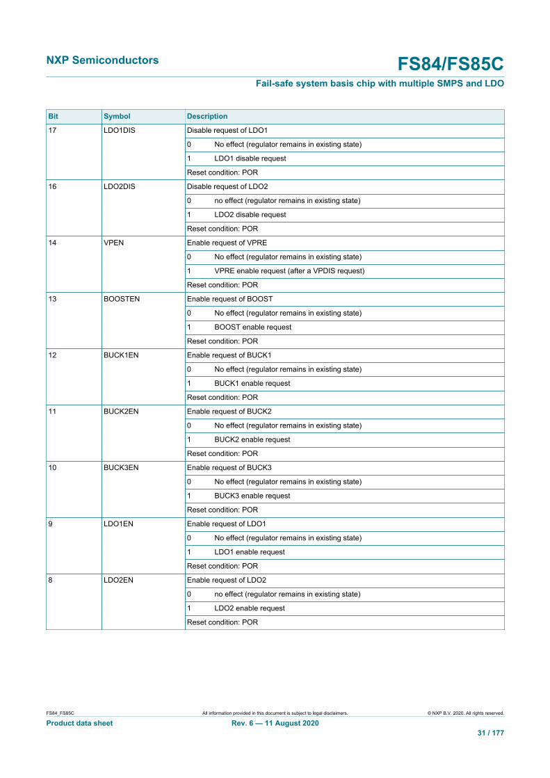
NXP Semiconductors FS84/FS85CFail-safe system basis chip with multiple SMPS and LDO
FS84_FS85C All information provided in this document is subject to legal disclaimers. © NXP B.V. 2020. All rights reserved.
Product data sheet Rev. 6 — 11 August 202031 / 177
Bit Symbol Description
Disable request of LDO1
0 No effect (regulator remains in existing state)
1 LDO1 disable request
17 LDO1DIS
Reset condition: POR
Disable request of LDO2
0 no effect (regulator remains in existing state)
1 LDO2 disable request
16 LDO2DIS
Reset condition: POR
Enable request of VPRE
0 No effect (regulator remains in existing state)
1 VPRE enable request (after a VPDIS request)
14 VPEN
Reset condition: POR
Enable request of BOOST
0 No effect (regulator remains in existing state)
1 BOOST enable request
13 BOOSTEN
Reset condition: POR
Enable request of BUCK1
0 No effect (regulator remains in existing state)
1 BUCK1 enable request
12 BUCK1EN
Reset condition: POR
Enable request of BUCK2
0 No effect (regulator remains in existing state)
1 BUCK2 enable request
11 BUCK2EN
Reset condition: POR
Enable request of BUCK3
0 No effect (regulator remains in existing state)
1 BUCK3 enable request
10 BUCK3EN
Reset condition: POR
Enable request of LDO1
0 No effect (regulator remains in existing state)
1 LDO1 enable request
9 LDO1EN
Reset condition: POR
Enable request of LDO2
0 no effect (regulator remains in existing state)
1 LDO2 enable request
8 LDO2EN
Reset condition: POR

NXP Semiconductors FS84/FS85CFail-safe system basis chip with multiple SMPS and LDO
FS84_FS85C All information provided in this document is subject to legal disclaimers. © NXP B.V. 2020. All rights reserved.
Product data sheet Rev. 6 — 11 August 202032 / 177
16.6 M_REG_CTRL2 register
Table 17. M_REG_CTRL2 register bit allocationBit 23 22 21 20 19 18 17 16
Write VBSTSR[1:0] BOOSTTSDCFG
BUCK1TSDCFG
BUCK2TSDCFG
BUCK3TSDCFG
LDO1TSDCFG
LDO2TSDCFG
Read VBSTSR[1:0] BOOSTTSDCFG
BUCK1TSDCFG
BUCK2TSDCFG
BUCK3TSDCFG
LDO1TSDCFG
LDO2TSDCFG
Reset OTP OTP OTP OTP OTP OTP OTP OTP
Bit 15 14 13 12 11 10 9 8
Write 0 0 0 VPRESRLS[1:0] 0 VPRESRHS[1:0]
Read RESERVED RESERVED RESERVED VPRESRLS[1:0] RESERVED VPRESRHS[1:0]
Reset 0 0 0 1 1 0 OTP OTP
Table 18. M_REG_CTRL2 register bit descriptionBit Symbol Description
VBOOST low-side slew rate control
00 50 V/μs - slow
01 100 V/μs – medium
10 300 V/μs – fast
11 500 V/μs – ultra fast
23 to 22 VBSTSR[1:0]
Reset condition: POR
BOOST behavior in case of TSD
0 Regulator shutdown
1 Regulator shutdown and state machine transition to DEEP-FS
21 BOOSTTSDCFG
Reset condition: POR
BUCK1 behavior in case of TSD
0 Regulator shutdown
1 Regulator shutdown and state machine transition to DEEP-FS
20 BUCK1TSDCFG
Reset condition: POR
BUCK2 behavior in case of TSD
0 Regulator shutdown
1 Regulator shutdown and state machine transition to DEEP-FS
19 BUCK2TSDCFG
Reset condition: POR
BUCK3 behavior in case of TSD
0 Regulator shutdown
1 Regulator shutdown and state machine transition to DEEP-FS
18 BUCK3TSDCFG
Reset condition: POR
LDO1 behavior in case of TSD
0 Regulator shutdown
1 Regulator shutdown and state machine transition to DEEP-FS
17 LDO1TSDCFG
Reset condition: POR
NXP Semiconductors FS84/FS85CFail-safe system basis chip with multiple SMPS and LDO
FS84_FS85C All information provided in this document is subject to legal disclaimers. © NXP B.V. 2020. All rights reserved.
Product data sheet Rev. 6 — 11 August 202033 / 177
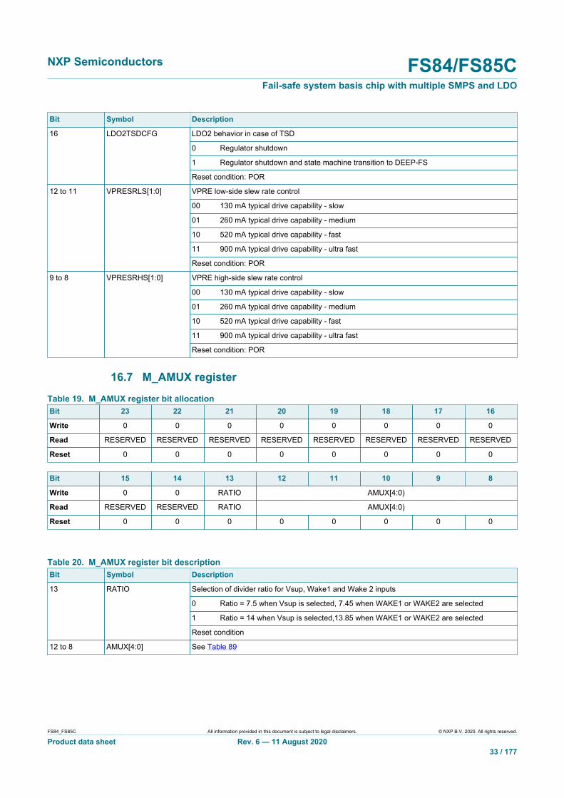
Bit Symbol Description
LDO2 behavior in case of TSD
0 Regulator shutdown
1 Regulator shutdown and state machine transition to DEEP-FS
16 LDO2TSDCFG
Reset condition: POR
VPRE low-side slew rate control
00 130 mA typical drive capability - slow
01 260 mA typical drive capability - medium
10 520 mA typical drive capability - fast
11 900 mA typical drive capability - ultra fast
12 to 11 VPRESRLS[1:0]
Reset condition: POR
VPRE high-side slew rate control
00 130 mA typical drive capability - slow
01 260 mA typical drive capability - medium
10 520 mA typical drive capability - fast
11 900 mA typical drive capability - ultra fast
9 to 8 VPRESRHS[1:0]
Reset condition: POR
16.7 M_AMUX register
Table 19. M_AMUX register bit allocationBit 23 22 21 20 19 18 17 16
Write 0 0 0 0 0 0 0 0
Read RESERVED RESERVED RESERVED RESERVED RESERVED RESERVED RESERVED RESERVED
Reset 0 0 0 0 0 0 0 0
Bit 15 14 13 12 11 10 9 8
Write 0 0 RATIO AMUX[4:0)
Read RESERVED RESERVED RATIO AMUX[4:0)
Reset 0 0 0 0 0 0 0 0
Table 20. M_AMUX register bit descriptionBit Symbol Description
Selection of divider ratio for Vsup, Wake1 and Wake 2 inputs
0 Ratio = 7.5 when Vsup is selected, 7.45 when WAKE1 or WAKE2 are selected
1 Ratio = 14 when Vsup is selected,13.85 when WAKE1 or WAKE2 are selected
13 RATIO
Reset condition
12 to 8 AMUX[4:0] See Table 89

NXP Semiconductors FS84/FS85CFail-safe system basis chip with multiple SMPS and LDO
FS84_FS85C All information provided in this document is subject to legal disclaimers. © NXP B.V. 2020. All rights reserved.
Product data sheet Rev. 6 — 11 August 202034 / 177
16.8 M_CLOCK register
Table 21. M_CLOCK register bit allocationBit 23 22 21 20 19 18 17 16
Write MOD_CONF FOUT_MUX_SEL[3:0] FOUT_PHASE[2:0]
Read MOD_CONF FOUT_MUX_SEL[3:0] FOUT_PHASE[2:0]
Reset 0 0 0 0 0 0 0 0
Bit 15 14 13 12 11 10 9 8
Write FOUT_CLK_SEL
EXT_FIN_SEL
FIN_DIV MOD_EN CLK_TUNE[3 :0]
Read FOUT_CLK_SEL
RESERVED FIN_DIV MOD_EN CLK_TUNE[3 :0]
Reset 0 0 0 0 0 0 0 0
Table 22. M_CLOCK register bit descriptionBit Symbol Description
Modulation configuration of main oscillator
0 range ± 5 % 23 kHz
1 range ± 5 % 94 kHz
23 MOD_CONF
Reset condition: POR
22 to 19 FOUT_MUX_SEL[3:0] See Table 87
FOUT phase shifting configuration (see Section 25.2 "Phase shifting")
000 No shift
001 Shifted by 1 clock cycle of CLK running at 20 MHz
010 Shifted by 2 clock cycle of CLK running at 20 MHz
011 Shifted by 3 clock cycle of CLK running at 20 MHz
100 Shifted by 4 clock cycle of CLK running at 20 MHz
101 Shifted by 5 clock cycle of CLK running at 20 MHz
110 Shifted by 6 clock cycle of CLK running at 20 MHz
111 Shifted by 7 clock cycle of CLK running at 20 MHz
18 to 16 FOUT_PHASE[2:0]
Reset condition: POR
FOUT_clk frequency selection (CLK1 or CLK2)
0 FOUT_clk = CLK1
1 FOUT_clk = CLK2
15 FOUT_CLK_SEL
Reset condition: POR
Enable request of EXT FIN selection at PLL input
0 No effect
1 FIN selection request
14 EXT_FIN_SEL
Reset condition: POR

NXP Semiconductors FS84/FS85CFail-safe system basis chip with multiple SMPS and LDO
FS84_FS85C All information provided in this document is subject to legal disclaimers. © NXP B.V. 2020. All rights reserved.
Product data sheet Rev. 6 — 11 August 202035 / 177
Bit Symbol Description
FIN input signal divider selection
0 Divider by 1
1 Divider by 6
13 FIN_DIV
Reset condition: POR
Modulation activation of main oscillator
0 Modulation disabled
1 Modulation enabled
12 MOD_EN
Reset condition: POR
11 to 8 CLK_TUNE[3:0] See Table 86
16.9 M_INT_MASK1 register
Table 23. M_INT_MASK1 register bit allocationBit 23 22 21 20 19 18 17 16
Write 0 VPREOC_M 0 BUCK1OC_M
BUCK2OC_M
BUCK3OC_M
LDO1OC_M LDO2OC_M
Read RESERVED VPREOC_M RESERVED BUCK1OC_M
BUCK2OC_M
BUCK3OC_M
LDO1OC_M LDO2OC_M
Reset 0 0 0 0 0 0 0 0
Bit 15 14 13 12 11 10 9 8
Write 0 0 BOOSTTSD_M
BUCK1TSD_M
BUCK2TSD_M
BUCK3TSD_M
LDO1TSD_M LDO2TSD_M
Read RESERVED RESERVED BOOSTTSD_M
BUCK1TSD_M
BUCK2TSD_M
BUCK3TSD_M
LDO1TSD_M LDO2TSD_M
Reset 0 0 0 0 0 0 0 0
Table 24. M_INT_MASK1 register bit descriptionBit Symbol Description
Inhibit INTERRUPT for VPRE overcurrent
0 INT not masked
1 INT masked
22 VPREOC_M
Reset condition: POR
Inhibit INTERRUPT for BUCK1 overcurrent
0 INT not masked
1 INT masked
20 BUCK1OC_M
Reset condition: POR
Inhibit INTERRUPT for BUCK3 overcurrent
0 INT not masked
1 INT masked
19 BUCK2OC_M
Reset condition: POR

NXP Semiconductors FS84/FS85CFail-safe system basis chip with multiple SMPS and LDO
FS84_FS85C All information provided in this document is subject to legal disclaimers. © NXP B.V. 2020. All rights reserved.
Product data sheet Rev. 6 — 11 August 202036 / 177
Bit Symbol Description
Inhibit INTERRUPT for BUCK3 overcurrent
0 INT not masked
1 INT masked
18 BUCK3OC_M
Reset condition: POR
Inhibit INTERRUPT for LDO1 overcurrent
0 INT not masked
1 INT masked
17 LDO1OC_M
Reset condition: POR
Inhibit INTERRUPT for LDO2 overcurrent
0 INT not masked
1 INT masked
16 LDO2OC_M
Reset condition: POR
Inhibit INTERRUPT for BOOST overtemperature shutdown event
0 INT not masked
1 INT masked
13 BOOSTTSD_M
Reset condition: POR
Inhibit INTERRUPT for BUCK1 overtemperature shutdown event
0 INT not masked
1 INT masked
12 BUCK1TSD_M
Reset condition: POR
Inhibit INTERRUPT for BUCK2 overtemperature shutdown event
0 INT not masked
1 INT masked
11 BUCK2TSD_M
Reset condition: POR
Inhibit INTERRUPT for BUCK3 overtemperature shutdown event
0 INT not masked
1 INT masked
10 BUCK3TSD_M
Reset condition: POR
Inhibit INTERRUPT for LDO1 overtemperature shutdown event
0 INT not masked
1 INT masked
9 LDO1TSD_M
Reset condition: POR
Inhibit INTERRUPT for LDO2 overtemperature shutdown event
0 INT not masked
1 INT masked
8 LDO2TSD_M
Reset condition: POR
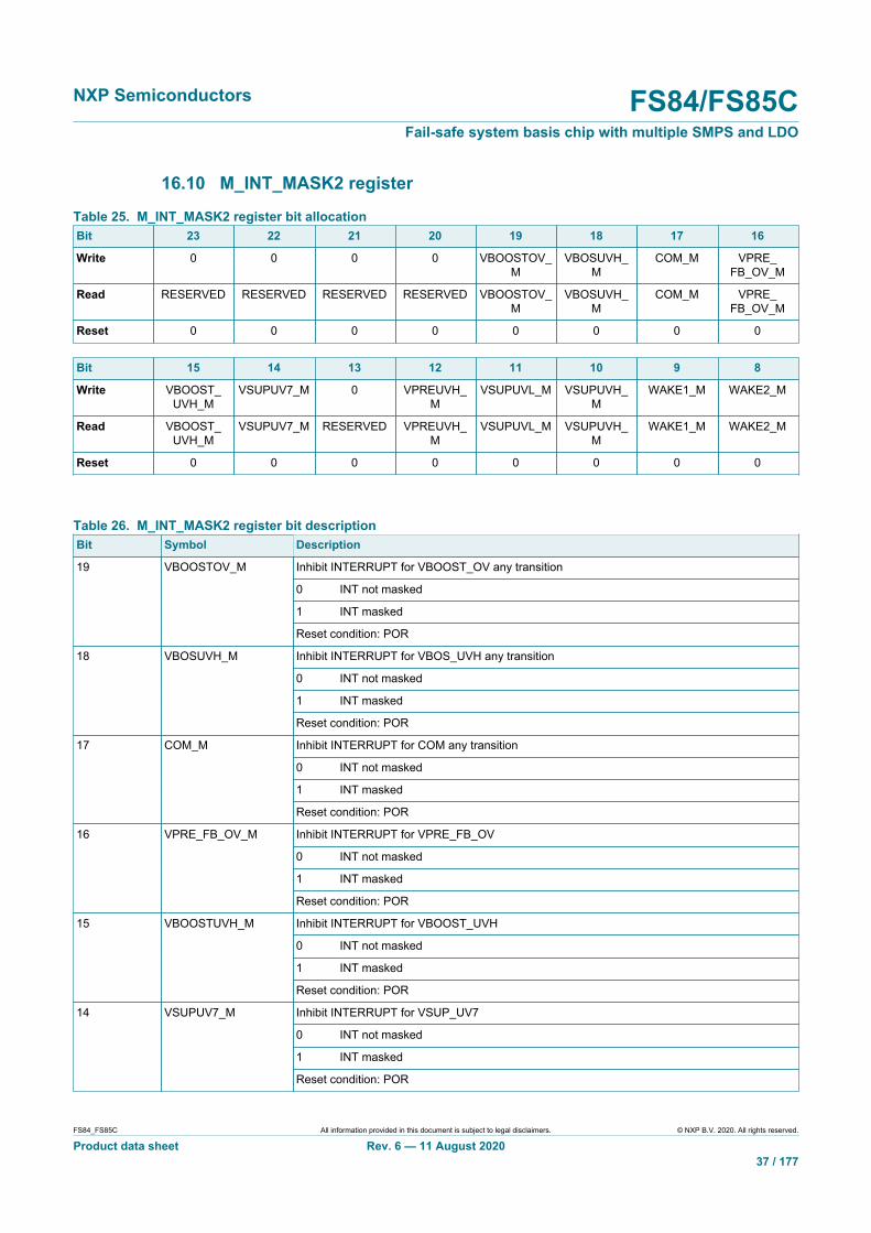
NXP Semiconductors FS84/FS85CFail-safe system basis chip with multiple SMPS and LDO
FS84_FS85C All information provided in this document is subject to legal disclaimers. © NXP B.V. 2020. All rights reserved.
Product data sheet Rev. 6 — 11 August 202037 / 177
16.10 M_INT_MASK2 register
Table 25. M_INT_MASK2 register bit allocationBit 23 22 21 20 19 18 17 16
Write 0 0 0 0 VBOOSTOV_M
VBOSUVH_M
COM_M VPRE_FB_OV_M
Read RESERVED RESERVED RESERVED RESERVED VBOOSTOV_M
VBOSUVH_M
COM_M VPRE_FB_OV_M
Reset 0 0 0 0 0 0 0 0
Bit 15 14 13 12 11 10 9 8
Write VBOOST_UVH_M
VSUPUV7_M 0 VPREUVH_M
VSUPUVL_M VSUPUVH_M
WAKE1_M WAKE2_M
Read VBOOST_UVH_M
VSUPUV7_M RESERVED VPREUVH_M
VSUPUVL_M VSUPUVH_M
WAKE1_M WAKE2_M
Reset 0 0 0 0 0 0 0 0
Table 26. M_INT_MASK2 register bit descriptionBit Symbol Description
Inhibit INTERRUPT for VBOOST_OV any transition
0 INT not masked
1 INT masked
19 VBOOSTOV_M
Reset condition: POR
Inhibit INTERRUPT for VBOS_UVH any transition
0 INT not masked
1 INT masked
18 VBOSUVH_M
Reset condition: POR
Inhibit INTERRUPT for COM any transition
0 INT not masked
1 INT masked
17 COM_M
Reset condition: POR
Inhibit INTERRUPT for VPRE_FB_OV
0 INT not masked
1 INT masked
16 VPRE_FB_OV_M
Reset condition: POR
Inhibit INTERRUPT for VBOOST_UVH
0 INT not masked
1 INT masked
15 VBOOSTUVH_M
Reset condition: POR
Inhibit INTERRUPT for VSUP_UV7
0 INT not masked
1 INT masked
14 VSUPUV7_M
Reset condition: POR

NXP Semiconductors FS84/FS85CFail-safe system basis chip with multiple SMPS and LDO
FS84_FS85C All information provided in this document is subject to legal disclaimers. © NXP B.V. 2020. All rights reserved.
Product data sheet Rev. 6 — 11 August 202038 / 177
Bit Symbol Description
Inhibit INTERRUPT for VSUP_UVH
0 INT not masked
1 INT masked
12 VREUVH_M
Reset condition: POR
Inhibit INTERRUPT for VSUP_UVL
0 INT not masked
1 INT masked
11 VSUPUVL_M
Reset condition: POR
Inhibit INTERRUPT for VPRE_UVH
0 INT not masked
1 INT masked
10 VSUPUVH_M
Reset condition: POR
Inhibit INTERRUPT for WAKE1 any transition
0 INT not masked
1 INT masked
9 WAKE1_M
Reset condition: POR
Inhibit INTERRUPT for WAKE2 any transition
0 INT not masked
1 INT masked
8 WAKE2_M
Reset condition: POR
16.11 M_FLAG1 registerWhen the device starts up, it is recommended to clear all the flags by writing 1s on allbits.
Table 27. M_FLAG1 register bit allocationBit 23 22 21 20 19 18 17 16
Write VBOSUVH VBOOSTUVH
VPREOC BUCK1OC BUCK2OC BUCK3OC LDO1OC LDO2OC
Read VBOSUVH VBOOSTUVH
VPREOC BUCK1OC BUCK2OC BUCK3OC LDO1OC LDO2OC
Reset 1 1 0 0 0 0 0 0
Bit 15 14 13 12 11 10 9 8
Write 0 VBOOSTOV VBOOSTOT BUCK1OT BUCK2OT BUCK3OT LDO1OT LDO2OT
Read CLK_FIN_DIV_OK
VBOOSTOV VBOOSTOT BUCK1OT BUCK2OT BUCK3OT LDO1OT LDO2OT
Reset 0 0 0 0 0 0 0 0
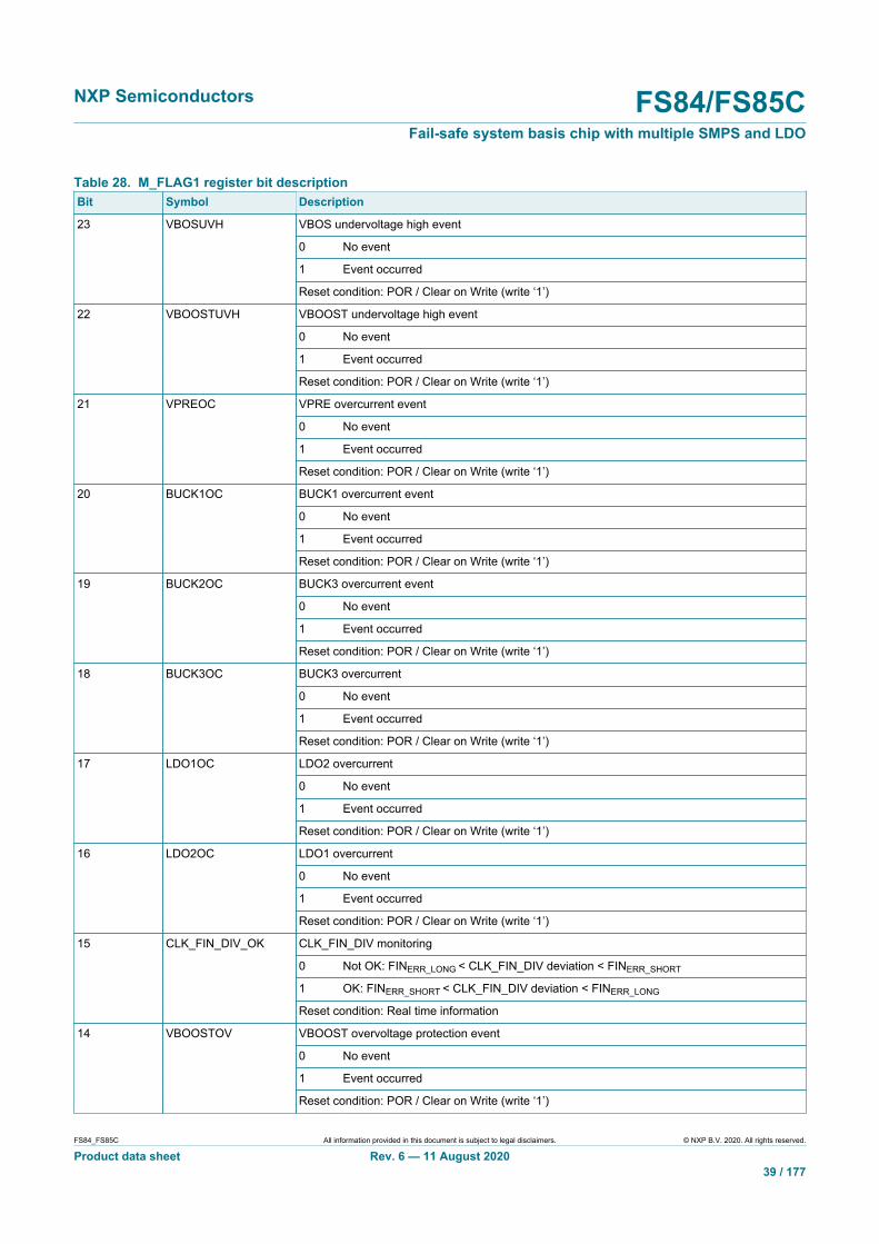
NXP Semiconductors FS84/FS85CFail-safe system basis chip with multiple SMPS and LDO
FS84_FS85C All information provided in this document is subject to legal disclaimers. © NXP B.V. 2020. All rights reserved.
Product data sheet Rev. 6 — 11 August 202039 / 177
Table 28. M_FLAG1 register bit descriptionBit Symbol Description
VBOS undervoltage high event
0 No event
1 Event occurred
23 VBOSUVH
Reset condition: POR / Clear on Write (write ‘1’)
VBOOST undervoltage high event
0 No event
1 Event occurred
22 VBOOSTUVH
Reset condition: POR / Clear on Write (write ‘1’)
VPRE overcurrent event
0 No event
1 Event occurred
21 VPREOC
Reset condition: POR / Clear on Write (write ‘1’)
BUCK1 overcurrent event
0 No event
1 Event occurred
20 BUCK1OC
Reset condition: POR / Clear on Write (write ‘1’)
BUCK3 overcurrent event
0 No event
1 Event occurred
19 BUCK2OC
Reset condition: POR / Clear on Write (write ‘1’)
BUCK3 overcurrent
0 No event
1 Event occurred
18 BUCK3OC
Reset condition: POR / Clear on Write (write ‘1’)
LDO2 overcurrent
0 No event
1 Event occurred
17 LDO1OC
Reset condition: POR / Clear on Write (write ‘1’)
LDO1 overcurrent
0 No event
1 Event occurred
16 LDO2OC
Reset condition: POR / Clear on Write (write ‘1’)
CLK_FIN_DIV monitoring
0 Not OK: FINERR_LONG < CLK_FIN_DIV deviation < FINERR_SHORT
1 OK: FINERR_SHORT < CLK_FIN_DIV deviation < FINERR_LONG
15 CLK_FIN_DIV_OK
Reset condition: Real time information
VBOOST overvoltage protection event
0 No event
1 Event occurred
14 VBOOSTOV
Reset condition: POR / Clear on Write (write ‘1’)

NXP Semiconductors FS84/FS85CFail-safe system basis chip with multiple SMPS and LDO
FS84_FS85C All information provided in this document is subject to legal disclaimers. © NXP B.V. 2020. All rights reserved.
Product data sheet Rev. 6 — 11 August 202040 / 177
Bit Symbol Description
VBOOST overtemperature shutdown event
0 No event
1 Event occurred
13 VBOOSTOT
Reset condition: POR / Clear on Write (write ‘1’)
BUCK1 overtemperature shutdown event
0 No event
1 Event occurred
12 BUCK1OT
Reset condition: POR / Clear on Write (write ‘1’)
BUCK2 overtemperature shutdown event
0 No event
1 Event occurred
11 BUCK2OT
Reset condition: POR / Clear on Write (write ‘1’)
BUCK3 overtemperature shutdown event
0 No event
1 Event occurred
10 BUCK3OT
Reset condition: POR / Clear on Write (write ‘1’)
LDO1 overtemperature shutdown event
0 No event
1 Event occurred
9 LDO1OT
Reset condition: POR / Clear on Write (write ‘1’)
LDO2 overtemperature shutdown event
0 No event
1 Event occurred
8 LDO2OT
Reset condition: POR / Clear on Write (write ‘1’)
16.12 M_FLAG2 registerWhen the device starts up, it is recommended to clear all the flags by writing 1s on allbits.
Table 29. M_FLAG2 register bit allocationBit 23 22 21 20 19 18 17 16
Write VPRE_FB_OV
VSUPUV7 0 0 0 0 0 0
Read VPRE_FB_OV
VSUPUV7 BOOST_ST BUCK1_ST BUCK2_ST BUCK3_ST LDO1_ST LDO2_ST
Reset 0 1 1 1 1 1 1 1
Bit 15 14 13 12 11 10 9 8
Write VPREUVL VPREUVH VSUPUVL VSUPUVH 0 0 WK2FLG WK1FLG
Read VPREUVL VPREUVH VSUPUVL VSUPUVH WK2RT WK1RT WK2FLG WK1FLG
Reset 1 1 1 1 0 1 0 1
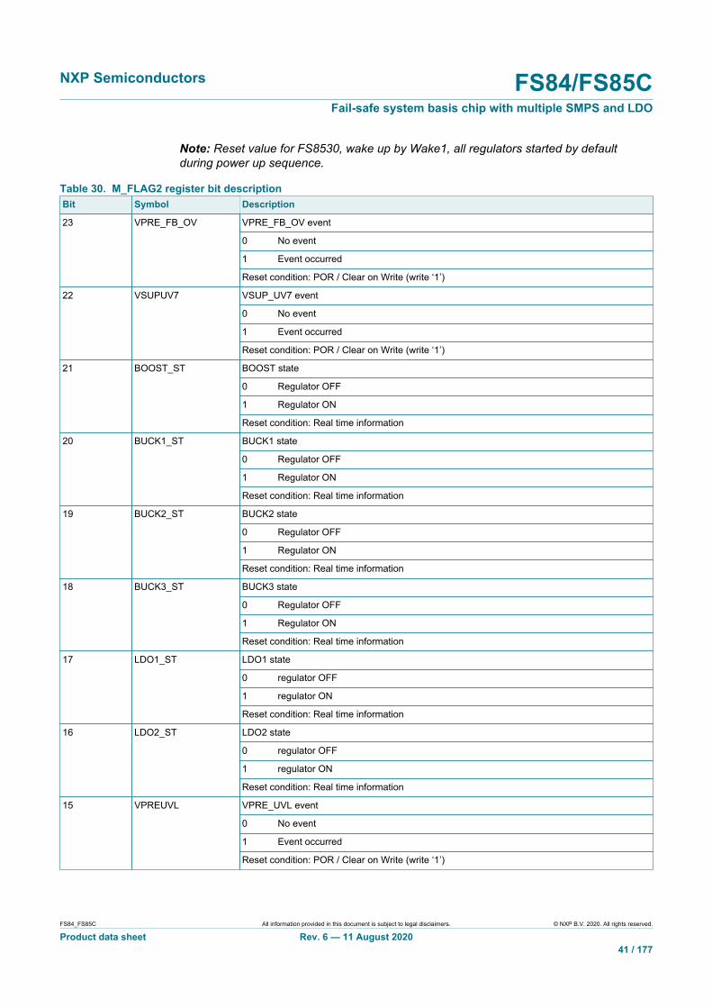
NXP Semiconductors FS84/FS85CFail-safe system basis chip with multiple SMPS and LDO
FS84_FS85C All information provided in this document is subject to legal disclaimers. © NXP B.V. 2020. All rights reserved.
Product data sheet Rev. 6 — 11 August 202041 / 177
Note: Reset value for FS8530, wake up by Wake1, all regulators started by defaultduring power up sequence.
Table 30. M_FLAG2 register bit descriptionBit Symbol Description
VPRE_FB_OV event
0 No event
1 Event occurred
23 VPRE_FB_OV
Reset condition: POR / Clear on Write (write ‘1’)
VSUP_UV7 event
0 No event
1 Event occurred
22 VSUPUV7
Reset condition: POR / Clear on Write (write ‘1’)
BOOST state
0 Regulator OFF
1 Regulator ON
21 BOOST_ST
Reset condition: Real time information
BUCK1 state
0 Regulator OFF
1 Regulator ON
20 BUCK1_ST
Reset condition: Real time information
BUCK2 state
0 Regulator OFF
1 Regulator ON
19 BUCK2_ST
Reset condition: Real time information
BUCK3 state
0 Regulator OFF
1 Regulator ON
18 BUCK3_ST
Reset condition: Real time information
LDO1 state
0 regulator OFF
1 regulator ON
17 LDO1_ST
Reset condition: Real time information
LDO2 state
0 regulator OFF
1 regulator ON
16 LDO2_ST
Reset condition: Real time information
VPRE_UVL event
0 No event
1 Event occurred
15 VPREUVL
Reset condition: POR / Clear on Write (write ‘1’)
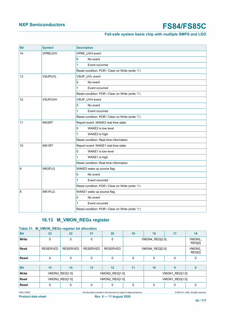
NXP Semiconductors FS84/FS85CFail-safe system basis chip with multiple SMPS and LDO
FS84_FS85C All information provided in this document is subject to legal disclaimers. © NXP B.V. 2020. All rights reserved.
Product data sheet Rev. 6 — 11 August 202042 / 177
Bit Symbol Description
VPRE_UVH event
0 No event
1 Event occurred
14 VPREUVH
Reset condition: POR / Clear on Write (write ‘1’)
VSUP_UVL event
0 No event
1 Event occurred
13 VSUPUVL
Reset condition: POR / Clear on Write (write ‘1’)
VSUP_UVH event
0 No event
1 Event occurred
12 VSUPUVH
Reset condition: POR / Clear on Write (write ‘1’)
Report event: WAKE2 real time state
0 WAKE2 is low level
1 WAKE2 is high
11 WK2RT
Reset condition: Real time information
Report event: WAKE1 real time state
0 WAKE1 is low level
1 WAKE1 is high
10 WK1RT
Reset condition: Real time information
WAKE2 wake up source flag
0 No event
1 Event occurred
9 WK2FLG
Reset condition: POR / Clear on Write (write ‘1’)
WAKE1 wake up source flag
0 No event
1 Event occurred
8 WK1FLG
Reset condition: POR / Clear on Write (write ‘1’)
16.13 M_VMON_REGx register
Table 31. M_VMON_REGx register bit allocationBit 23 22 21 20 19 18 17 16
Write 0 0 0 0 VMON4_REG[2:0] VMON3_REG[2]
Read RESERVED RESERVED RESERVED RESERVED VMON4_REG[2:0] VMON3_REG[2]
Reset 0 0 0 0 0 0 0 0
Bit 15 14 13 12 11 10 9 8
Write VMON3_REG[1:0] VMON2_REG[1:0] VMON1_REG[1:0]
Read VMON3_REG[1:0] VMON2_REG[1:0] VMON1_REG[1:0]
Reset 0 0 0 0 0 0 0 0
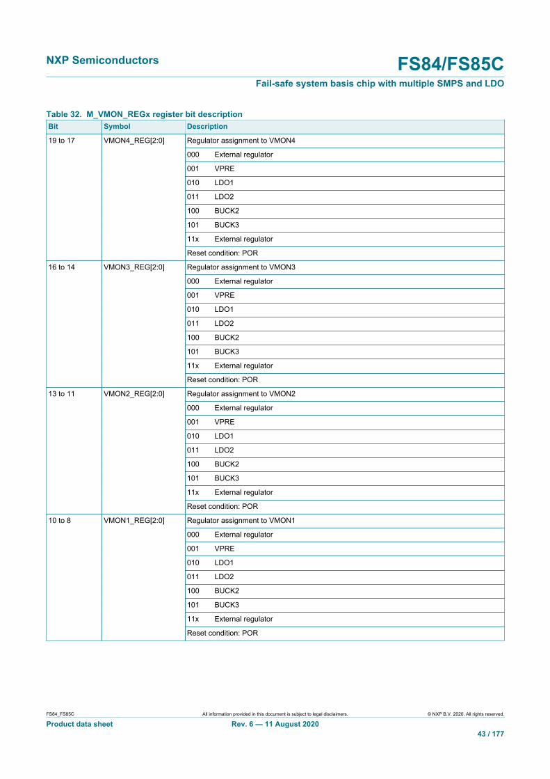
NXP Semiconductors FS84/FS85CFail-safe system basis chip with multiple SMPS and LDO
FS84_FS85C All information provided in this document is subject to legal disclaimers. © NXP B.V. 2020. All rights reserved.
Product data sheet Rev. 6 — 11 August 202043 / 177
Table 32. M_VMON_REGx register bit descriptionBit Symbol Description
Regulator assignment to VMON4
000 External regulator
001 VPRE
010 LDO1
011 LDO2
100 BUCK2
101 BUCK3
11x External regulator
19 to 17 VMON4_REG[2:0]
Reset condition: POR
Regulator assignment to VMON3
000 External regulator
001 VPRE
010 LDO1
011 LDO2
100 BUCK2
101 BUCK3
11x External regulator
16 to 14 VMON3_REG[2:0]
Reset condition: POR
Regulator assignment to VMON2
000 External regulator
001 VPRE
010 LDO1
011 LDO2
100 BUCK2
101 BUCK3
11x External regulator
13 to 11 VMON2_REG[2:0]
Reset condition: POR
Regulator assignment to VMON1
000 External regulator
001 VPRE
010 LDO1
011 LDO2
100 BUCK2
101 BUCK3
11x External regulator
10 to 8 VMON1_REG[2:0]
Reset condition: POR
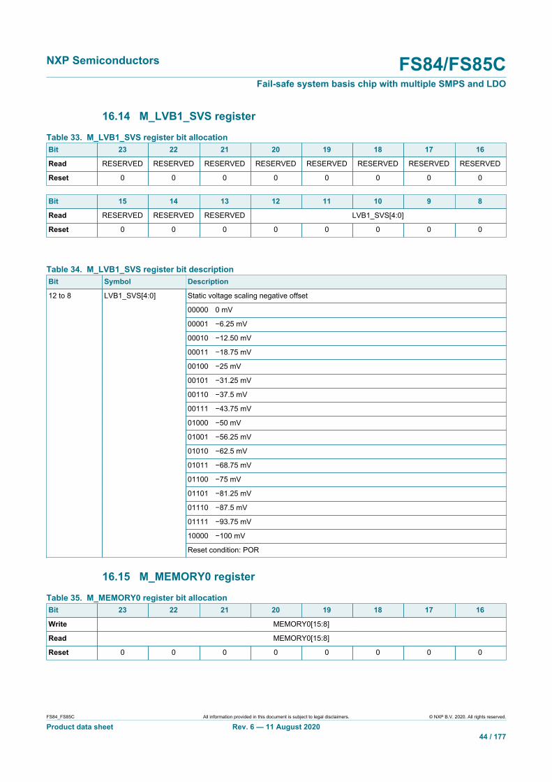
NXP Semiconductors FS84/FS85CFail-safe system basis chip with multiple SMPS and LDO
FS84_FS85C All information provided in this document is subject to legal disclaimers. © NXP B.V. 2020. All rights reserved.
Product data sheet Rev. 6 — 11 August 202044 / 177
16.14 M_LVB1_SVS register
Table 33. M_LVB1_SVS register bit allocationBit 23 22 21 20 19 18 17 16
Read RESERVED RESERVED RESERVED RESERVED RESERVED RESERVED RESERVED RESERVED
Reset 0 0 0 0 0 0 0 0
Bit 15 14 13 12 11 10 9 8
Read RESERVED RESERVED RESERVED LVB1_SVS[4:0]
Reset 0 0 0 0 0 0 0 0
Table 34. M_LVB1_SVS register bit descriptionBit Symbol Description
Static voltage scaling negative offset
00000 0 mV
00001 −6.25 mV
00010 −12.50 mV
00011 −18.75 mV
00100 −25 mV
00101 −31.25 mV
00110 −37.5 mV
00111 −43.75 mV
01000 −50 mV
01001 −56.25 mV
01010 −62.5 mV
01011 −68.75 mV
01100 −75 mV
01101 −81.25 mV
01110 −87.5 mV
01111 −93.75 mV
10000 −100 mV
12 to 8 LVB1_SVS[4:0]
Reset condition: POR
16.15 M_MEMORY0 register
Table 35. M_MEMORY0 register bit allocationBit 23 22 21 20 19 18 17 16
Write MEMORY0[15:8]
Read MEMORY0[15:8]
Reset 0 0 0 0 0 0 0 0
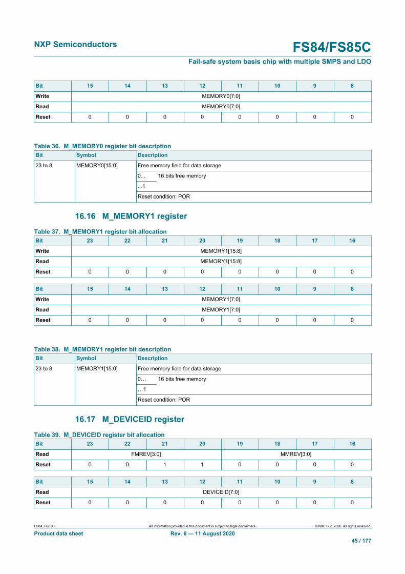
NXP Semiconductors FS84/FS85CFail-safe system basis chip with multiple SMPS and LDO
FS84_FS85C All information provided in this document is subject to legal disclaimers. © NXP B.V. 2020. All rights reserved.
Product data sheet Rev. 6 — 11 August 202045 / 177
Bit 15 14 13 12 11 10 9 8
Write MEMORY0[7:0]
Read MEMORY0[7:0]
Reset 0 0 0 0 0 0 0 0
Table 36. M_MEMORY0 register bit descriptionBit Symbol Description
Free memory field for data storage
0...
...1
16 bits free memory
23 to 8 MEMORY0[15:0]
Reset condition: POR
16.16 M_MEMORY1 register
Table 37. M_MEMORY1 register bit allocationBit 23 22 21 20 19 18 17 16
Write MEMORY1[15:8]
Read MEMORY1[15:8]
Reset 0 0 0 0 0 0 0 0
Bit 15 14 13 12 11 10 9 8
Write MEMORY1[7:0]
Read MEMORY1[7:0]
Reset 0 0 0 0 0 0 0 0
Table 38. M_MEMORY1 register bit descriptionBit Symbol Description
Free memory field for data storage
0…
…1
16 bits free memory
23 to 8 MEMORY1[15:0]
Reset condition: POR
16.17 M_DEVICEID register
Table 39. M_DEVICEID register bit allocationBit 23 22 21 20 19 18 17 16
Read FMREV[3:0] MMREV[3:0]
Reset 0 0 1 1 0 0 0 0
Bit 15 14 13 12 11 10 9 8
Read DEVICEID[7:0]
Reset 0 0 0 0 0 0 0 0

NXP Semiconductors FS84/FS85CFail-safe system basis chip with multiple SMPS and LDO
FS84_FS85C All information provided in this document is subject to legal disclaimers. © NXP B.V. 2020. All rights reserved.
Product data sheet Rev. 6 — 11 August 202046 / 177
Table 40. M_DEVICEID register bit descriptionBit Symbol Description
Full mask revision
Full mask revision configured by metal connection
23 to 20 FMREV[3:0]
Reset condition: POR
Metal Mask Revision
Metal mask revision configured by metal connection
19 to 16 MMREV[3:0]
Reset condition: POR
Device ID
x…x Device ID from OTP_DEVICEID[7:0] bits
15 to 8 DEVICEID[7:0]
Reset condition: POR
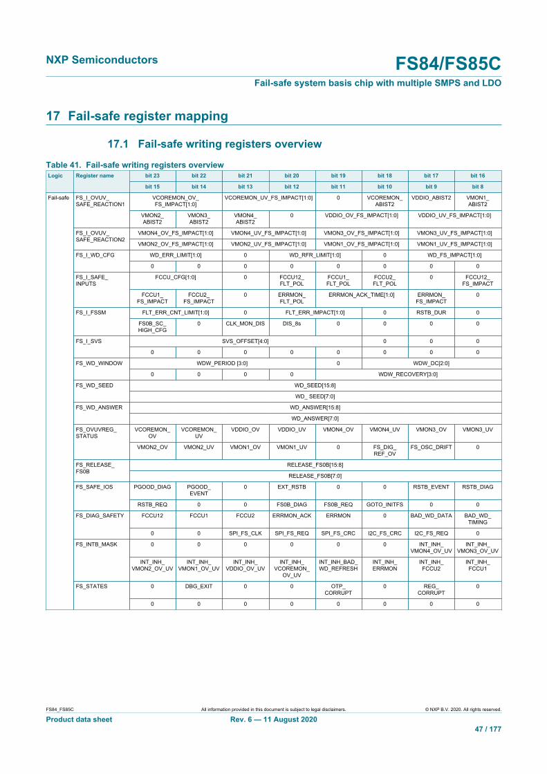
NXP Semiconductors FS84/FS85CFail-safe system basis chip with multiple SMPS and LDO
FS84_FS85C All information provided in this document is subject to legal disclaimers. © NXP B.V. 2020. All rights reserved.
Product data sheet Rev. 6 — 11 August 202047 / 177
17 Fail-safe register mapping
17.1 Fail-safe writing registers overview
Table 41. Fail-safe writing registers overviewbit 23 bit 22 bit 21 bit 20 bit 19 bit 18 bit 17 bit 16Logic Register name
bit 15 bit 14 bit 13 bit 12 bit 11 bit 10 bit 9 bit 8
VCOREMON_OV_FS_IMPACT[1:0]
VCOREMON_UV_FS_IMPACT[1:0] 0 VCOREMON_ABIST2
VDDIO_ABIST2 VMON1_ABIST2
FS_I_OVUV_SAFE_REACTION1
VMON2_ABIST2
VMON3_ABIST2
VMON4_ABIST2
0 VDDIO_OV_FS_IMPACT[1:0] VDDIO_UV_FS_IMPACT[1:0]
VMON4_OV_FS_IMPACT[1:0] VMON4_UV_FS_IMPACT[1:0] VMON3_OV_FS_IMPACT[1:0] VMON3_UV_FS_IMPACT[1:0]FS_I_OVUV_SAFE_REACTION2
VMON2_OV_FS_IMPACT[1:0] VMON2_UV_FS_IMPACT[1:0] VMON1_OV_FS_IMPACT[1:0] VMON1_UV_FS_IMPACT[1:0]
WD_ERR_LIMIT[1:0] 0 WD_RFR_LIMIT[1:0] 0 WD_FS_IMPACT[1:0]FS_I_WD_CFG
0 0 0 0 0 0 0 0
FCCU_CFG[1:0] 0 FCCU12_FLT_POL
FCCU1_FLT_POL
FCCU2_FLT_POL
0 FCCU12_FS_IMPACT
FS_I_SAFE_INPUTS
FCCU1_FS_IMPACT
FCCU2_FS_IMPACT
0 ERRMON_FLT_POL
ERRMON_ACK_TIME[1:0] ERRMON_FS_IMPACT
0
FLT_ERR_CNT_LIMIT[1:0] 0 FLT_ERR_IMPACT[1:0] 0 RSTB_DUR 0FS_I_FSSM
FS0B_SC_HIGH_CFG
0 CLK_MON_DIS DIS_8s 0 0 0 0
SVS_OFFSET[4:0] 0 0 0FS_I_SVS
0 0 0 0 0 0 0 0
WDW_PERIOD [3:0] 0 WDW_DC[2:0]FS_WD_WINDOW
0 0 0 0 WDW_RECOVERY[3:0]
WD_SEED[15:8]FS_WD_SEED
WD_ SEED[7:0]
WD_ANSWER[15:8]FS_WD_ANSWER
WD_ANSWER[7:0]
VCOREMON_OV
VCOREMON_UV
VDDIO_OV VDDIO_UV VMON4_OV VMON4_UV VMON3_OV VMON3_UVFS_OVUVREG_STATUS
VMON2_OV VMON2_UV VMON1_OV VMON1_UV 0 FS_DIG_REF_OV
FS_OSC_DRIFT 0
RELEASE_FS0B[15:8]FS_RELEASE_FS0B
RELEASE_FS0B[7:0]
PGOOD_DIAG PGOOD_EVENT
0 EXT_RSTB 0 0 RSTB_EVENT RSTB_DIAGFS_SAFE_IOS
RSTB_REQ 0 0 FS0B_DIAG FS0B_REQ GOTO_INITFS 0 0
FCCU12 FCCU1 FCCU2 ERRMON_ACK ERRMON 0 BAD_WD_DATA BAD_WD_TIMING
FS_DIAG_SAFETY
0 0 SPI_FS_CLK SPI_FS_REQ SPI_FS_CRC I2C_FS_CRC I2C_FS_REQ 0
0 0 0 0 0 0 INT_INH_VMON4_OV_UV
INT_INH_VMON3_OV_UV
FS_INTB_MASK
INT_INH_VMON2_OV_UV
INT_INH_VMON1_OV_UV
INT_INH_VDDIO_OV_UV
INT_INH_VCOREMON_
OV_UV
INT_INH_BAD_WD_REFRESH
INT_INH_ERRMON
INT_INH_FCCU2
INT_INH_FCCU1
0 DBG_EXIT 0 0 OTP_CORRUPT
0 REG_CORRUPT
0
Fail-safe
FS_STATES
0 0 0 0 0 0 0 0

NXP Semiconductors FS84/FS85CFail-safe system basis chip with multiple SMPS and LDO
FS84_FS85C All information provided in this document is subject to legal disclaimers. © NXP B.V. 2020. All rights reserved.
Product data sheet Rev. 6 — 11 August 202048 / 177
17.2 Fail-safe reading registers overview
Table 42. Fail-safe reading registers overviewbit 23 bit 22 bit 21 bit 20 bit 19 bit 18 bit 17 bit 16Logic Register name
bit 15 bit 14 bit 13 bit 12 bit 11 bit 10 bit 9 bit 8
FS_COM_G FS_WD_G FS_IO_G FS_REG_OVUV_G
RESERVED RESERVED RESERVED RESERVEDFS_GRL_FLAGS
RESERVED RESERVED RESERVED RESERVED RESERVED RESERVED RESERVED RESERVED
VCOREMON_OV_FS_IMPACT[1:0]
VCOREMON_UV_FS_IMPACT[1:0] RESERVED VCOREMON_ABIST2
VDDIO_ABIST2 VMON1_ABIST2
FS_I_OVUV_SAFE_REACTION1
VMON2_ABIST2
VMON3_ABIST2
VMON4_ABIST2
RESERVED VDDIO_OV_FS_IMPACT[1:0] VDDIO_UV_FS_IMPACT[1:0]
VMON4_OV_FS_IMPACT[1:0] VMON4_UV_FS_IMPACT[1:0] VMON3_OV_FS_IMPACT[1:0] VMON3_UV_FS_IMPACT[1:0]FS_I_OVUV_SAFE_REACTION2
VMON2_OV_FS_IMPACT[1:0] VMON2_UV_FS_IMPACT[1:0] VMON1_OV_FS_IMPACT[1:0] VMON1_UV_FS_IMPACT[1:0]
WD_ERR_LIMIT[1:0] RESERVED WD_RFR_LIMIT[1:0] RESERVED WD_FS_IMPACT[1:0]FS_I_WD_CFG
RESERVED WD_RFR_CNT[2:0] WD_ERR_CNT[3:0]
FCCU_CFG[1:0] RESERVED FCCU12_FLT_POL
FCCU1_FLT_POL
FCCU2_FLT_POL
RESERVED FCCU12_FS_IMPACT
FS_I_SAFE_INPUTS
FCCU1_FS_IMPACT
FCCU2_FS_IMPACT
RESERVED ERRMON_FLT_POL
ERRMON_ACK_TIME[1:0] ERRMON_FS_IMPACT
RESERVED
FLT_ERR_CNT_LIMIT[1:0] RESERVED FLT_ERR_IMPACT[1:0] RESERVED RSTB_DUR RESERVEDFS_I_FSSM
FS0B_SC_HIGH_CFG
RESERVED CLK_MON_DIS DIS_8s FLT_ERR_CNT[3:0]
SVS_OFFSET[4:0] RESERVED RESERVED RESERVEDFS_I_SVS
RESERVED RESERVED reserved RESERVED RESERVED RESERVED RESERVED RESERVED
WDW_PERIOD[3:0] RESERVED WDW_DC[2:0]FS_WD_WINDOW
RESERVED RESERVED RESERVED RESERVED WDW_RECOVERY[3:0]
WD_ SEED[15:8]FS_WD_SEED
WD_ SEED[7:0]
WD_ANSWER[15:8]FS_WD_ANSWER
WD_ANSWER[7:0]
VCOREMON_OV
VCOREMON_UV
VDDIO_OV VDDIO_UV VMON4_OV VMON4_UV VMON3_OV VMON3_UVFS_OVUVREG_STATUS
VMON2_OV VMON2_UV VMON1_OV VMON1_UV RESERVED FS_DIG_REF_OV
FS_OSC_DRIFT RESERVED
RELEASE_FS0B[15:8]FS_RELEASE_FS0B
RELEASE_FS0B[7:0]
PGOOD_DIAG PGOOD_EVENT
PGOOD_SNS EXT_RSTB RSTB_DRV RSTB_SNS RSTB_EVENT RSTB_DIAGFS_SAFE_IOS
RESERVED FS0B_DRV FS0B_SNS FS0B_DIAG RESERVED RESERVED FCCU2_RT FCCU1_RT
FCCU12 FCCU1 FCCU2 RESERVED ERRMON ERRMON_STATUS
BAD_WD_DATA BAD_WD_TIMING
FS_DIAG_SAFETY
ABIST1_OK ABIST2_OK SPI_FS_CLK SPI_FS_REQ SPI_FS_CRC I2C_FS_CRC I2C_FS_REQ LBIST_OK
RESERVED RESERVED RESERVED RESERVED RESERVED RESERVED INT_INH_VMON4_OV_UV
INT_INH_VMON4_OV_UV
FS_INTB_MASK
INT_INH_VMON2_OV_UV
INT_INH_VMON1_OV_UV
INT_INH_VDDIO_OV_UV
INT_INH_VCOREMON_
OV_UV
INT_INH_BAD_WD_REFRESH
INT_INH_ERRMON
INT_INH_FCCU2
INT_INH_FCCU1
RESERVED RESERVED DBG_MODE RESERVED OTP_CORRUPT
RESERVED REG_CORRUPT
RESERVED
Fail-safe
FS_STATES
RESERVED RESERVED RESERVED FSM_STATE[4:0]
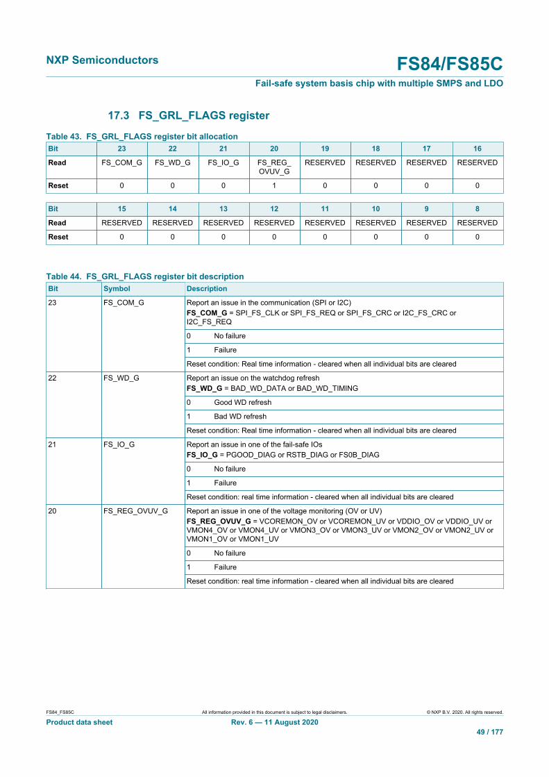
NXP Semiconductors FS84/FS85CFail-safe system basis chip with multiple SMPS and LDO
FS84_FS85C All information provided in this document is subject to legal disclaimers. © NXP B.V. 2020. All rights reserved.
Product data sheet Rev. 6 — 11 August 202049 / 177
17.3 FS_GRL_FLAGS register
Table 43. FS_GRL_FLAGS register bit allocationBit 23 22 21 20 19 18 17 16
Read FS_COM_G FS_WD_G FS_IO_G FS_REG_OVUV_G
RESERVED RESERVED RESERVED RESERVED
Reset 0 0 0 1 0 0 0 0
Bit 15 14 13 12 11 10 9 8
Read RESERVED RESERVED RESERVED RESERVED RESERVED RESERVED RESERVED RESERVED
Reset 0 0 0 0 0 0 0 0
Table 44. FS_GRL_FLAGS register bit descriptionBit Symbol Description
Report an issue in the communication (SPI or I2C)FS_COM_G = SPI_FS_CLK or SPI_FS_REQ or SPI_FS_CRC or I2C_FS_CRC orI2C_FS_REQ
0 No failure
1 Failure
23 FS_COM_G
Reset condition: Real time information - cleared when all individual bits are cleared
Report an issue on the watchdog refreshFS_WD_G = BAD_WD_DATA or BAD_WD_TIMING
0 Good WD refresh
1 Bad WD refresh
22 FS_WD_G
Reset condition: Real time information - cleared when all individual bits are cleared
Report an issue in one of the fail-safe IOsFS_IO_G = PGOOD_DIAG or RSTB_DIAG or FS0B_DIAG
0 No failure
1 Failure
21 FS_IO_G
Reset condition: real time information - cleared when all individual bits are cleared
Report an issue in one of the voltage monitoring (OV or UV)FS_REG_OVUV_G = VCOREMON_OV or VCOREMON_UV or VDDIO_OV or VDDIO_UV orVMON4_OV or VMON4_UV or VMON3_OV or VMON3_UV or VMON2_OV or VMON2_UV orVMON1_OV or VMON1_UV
0 No failure
1 Failure
20 FS_REG_OVUV_G
Reset condition: real time information - cleared when all individual bits are cleared

NXP Semiconductors FS84/FS85CFail-safe system basis chip with multiple SMPS and LDO
FS84_FS85C All information provided in this document is subject to legal disclaimers. © NXP B.V. 2020. All rights reserved.
Product data sheet Rev. 6 — 11 August 202050 / 177
17.4 FS_I_OVUV_SAFE_REACTION1 register
Table 45. FS_I_OVUV_SAFE_REACTION1 register bit allocationBit 23 22 21 20 19 18 17 16
Write VCOREMON_OV_FS_IMPACT[1:0]
VCOREMON_UV_FS_IMPACT[1:0]
0 VCOREMON_ABIST2
VDDIO_ABIST2
VMON1_ABIST2
Read VCOREMON_OV_FS_IMPACT[1:0]
VCOREMON_UV_FS_IMPACT[1:0]
RESERVED VCOREMON_ABIST2
VDDIO_ABIST2
VMON1_ABIST2
Reset 1 1 0 1 0 0 0 0
Bit 15 14 13 12 11 10 9 8
Write VMON2_ABIST2
VMON3_ABIST2
VMON4_ABIST2
0 VDDIO_OV_FS_IMPACT[1:0]
VDDIO_UV_FS_IMPACT[1:0]
Read VMON2_ABIST2
VMON3_ABIST2
VMON4_ABIST2
RESERVED VDDIO_OV_FS_IMPACT[1:0]
VDDIO_UV_FS_IMPACT[1:0]
Reset 0 0 0 0 1 1 0 1
Table 46. FS_I_OVUV_SAFE_REACTION1 register bit descriptionBit Symbol Description
23 to 22 VCOREMON_OV_FS_IMPACT[1:0] Table 117
21 to 20 VCOREMON_UV_FS_IMPACT[1:0] Table 117
VCOREMON ABIST2 configuration
0 No ABIST
1 VCOREMON BIST executed during ABIST2
18 VCOREMON_ABIST2
Reset condition: POR
VDDIO ABIST2 configuration
0 No ABIST
1 VDDIO BIST executed during ABIST2
17 VDDIO_ABIST2
Reset condition: POR
VMON1 ABIST2 configuration
0 No ABIST
1 VMON1 BIST executed during ABIST2
16 VMON1_ABIST2
Reset condition: POR
VMON2 ABIST2 configuration
0 No ABIST
1 VMON2 BIST executed during ABIST2
15 VMON2_ABIST2
Reset condition: POR
VMON3 ABIST2 configuration
0 No ABIST
1 VMON3 BIST executed during ABIST2
14 VMON3_ABIST2
Reset condition: POR

NXP Semiconductors FS84/FS85CFail-safe system basis chip with multiple SMPS and LDO
FS84_FS85C All information provided in this document is subject to legal disclaimers. © NXP B.V. 2020. All rights reserved.
Product data sheet Rev. 6 — 11 August 202051 / 177
Bit Symbol Description
VMON4 ABIST2 configuration
0 No ABIST
1 VMON4 BIST executed during ABIST2
13 VMON4_ABIST2
Reset condition: POR
11 to 10 VDDIO_OV_FS_IMPACT[1:0] Table 120
9 to 8 VDDIO_UV_FS_IMPACT[1:0] Table 120
17.5 FS_I_OVUV_SAFE_REACTION2 register
Table 47. FS_I_OVUV_SAFE_REACTION2 register bit allocationBit 23 22 21 20 19 18 17 16
Write VMON4_OV_FS_IMPACT[1:0]
VMON4_UV_FS_IMPACT[1:0]
VMON3_OV_FS_IMPACT[1:0]
VMON3_UV_FS_IMPACT[1:0]
Read VMON4_OV_FS_IMPACT[1:0]
VMON4_UV_FS_IMPACT[1:0]
VMON3_OV_FS_IMPACT[1:0]
VMON3_UV_FS_IMPACT[1:0]
Reset 1 1 0 1 1 1 0 1
Bit 15 14 13 12 11 10 9 8
Write VMON2_OV_FS_IMPACT[1:0]
VMON2_UV_FS_IMPACT[1:0]
VMON1_OV_FS_IMPACT[1:0]
VMON1_UV_FS_IMPACT[1:0]
Read VMON2_OV_FS_IMPACT[1:0]
VMON2_UV_FS_IMPACT[1:0]
VMON1_OV_FS_IMPACT[1:0]
VMON1_UV_FS_IMPACT[1:0]
Reset 1 1 0 1 1 1 0 1
Table 48. FS_I_OVUV_SAFE_REACTION2 register bit descriptionBit Symbol Description
23 to 22 VMON4_OV_FS_IMPACT[1:0]
21 to 20 VMON4_UV_FS_IMPACT[1:0]
19 to 18 VMON3_OV_FS_IMPACT[1:0]
17 to 16 VMON3_UV_FS_IMPACT[1:0]
15 to 14 VMON2_OV_FS_IMPACT[1:0]
13 to 12 VMON2_UV_FS_IMPACT[1:0]
11 to 10 VMON1_OV_FS_IMPACT[1:0]
9 to 8 VMON1_UV_FS_IMPACT[1:0]
See Table 122
17.6 FS_I_WD_CFG register
Table 49. FS_I_WD_CFG register bit allocationBit 23 22 21 20 19 18 17 16
Write WD_ERR_LIMIT[1:0] 0 WD_RFR_LIMIT[1:0] 0 WD_FS_IMPACT[1:0]
Read WD_ERR_LIMIT[1:0] RESERVED WD_RFR_LIMIT[1:0] RESERVED WD_FS_IMPACT[1:0]
Reset 0 1 0 0 0 0 1 0
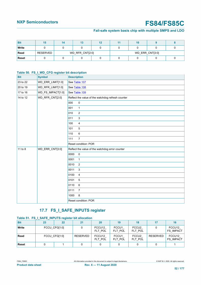
NXP Semiconductors FS84/FS85CFail-safe system basis chip with multiple SMPS and LDO
FS84_FS85C All information provided in this document is subject to legal disclaimers. © NXP B.V. 2020. All rights reserved.
Product data sheet Rev. 6 — 11 August 202052 / 177
Bit 15 14 13 12 11 10 9 8
Write 0 0 0 0 0 0 0 0
Read RESERVED WD_RFR_CNT[2:0] WD_ERR_CNT[3:0]
Reset 0 0 0 0 0 0 0 0
Table 50. FS_I_WD_CFG register bit descriptionBit Symbol Description
23 to 22 WD_ERR_LIMIT[1:0] See Table 107
20 to 19 WD_RFR_LIMIT[1:0] See Table 108
17 to 16 WD_FS_IMPACT[1:0] See Table 109
Reflect the value of the watchdog refresh counter
000 0
001 1
010 2
011 3
100 4
101 5
110 6
111 7
14 to 12 WD_RFR_CNT[2:0]
Reset condition: POR
Reflect the value of the watchdog error counter
0000 0
0001 1
0010 2
0011 3
0100 4
0101 5
0110 6
0111 7
1000 8
11 to 8 WD_ERR_CNT[3:0]
Reset condition: POR
17.7 FS_I_SAFE_INPUTS register
Table 51. FS_I_SAFE_INPUTS register bit allocationBit 23 22 21 20 19 18 17 16
Write FCCU_CFG[1:0] 0 FCCU12_FLT_POL
FCCU1_FLT_POL
FCCU2_FLT_POL
0 FCCU12_FS_IMPACT
Read FCCU_CFG[1:0] RESERVED FCCU12_FLT_POL
FCCU1_FLT_POL
FCCU2_FLT_POL
RESERVED FCCU12_FS_IMPACT
Reset 0 1 0 0 0 0 0 1

NXP Semiconductors FS84/FS85CFail-safe system basis chip with multiple SMPS and LDO
FS84_FS85C All information provided in this document is subject to legal disclaimers. © NXP B.V. 2020. All rights reserved.
Product data sheet Rev. 6 — 11 August 202053 / 177
Bit 15 14 13 12 11 10 9 8
Write FCCU1_FS_IMPACT
FCCU2_FS_IMPACT
0 ERRMON_FLT_POL
ERRMON_ACK_TIME[1:0] ERRMON_FS_IMPACT
0
Read FCCU1_FS_IMPACT
FCCU2_FS_IMPACT
RESERVED ERRMON_FLT_POL
ERRMON_ACK_TIME[1:0] ERRMON_FS_IMPACT
RESERVED
Reset 1 1 0 0 0 1 1 0
Table 52. FS_I_SAFE_INPUTS register bit descriptionBit Symbol Description
23 to 22 FCCU_CFG[1:0] See Table 111
20 FCCU12_FLT_POL See Table 112
19 FCCU1_FLT_POL See Table 114
18 FCCU2_FLT_POL See Table 114
16 FCCU12_FS_IMPACT See Table 113
15 FCCU1_FS_IMPACT See Table 115
14 FCCU2_FS_IMPACT See Table 115
12 ERRMON_FLT_POL See Table 124
11 to 10 ERRMON_ACK_TIME[1:0] See Table 125
9 ERRMON_FS_IMPACT See Table 126
17.8 FS_I_FSSM register
Table 53. FS_I_FSSM register bit allocationBit 23 22 21 20 19 18 17 16
Write FLT_ERR_CNT_LIMIT[1:0] 0 FLT_ERR_IMPACT[1:0] 0 RSTB_DUR 0
Read FLT_ERR_CNT_LIMIT[1:0] RESERVED FLT_ERR_IMPACT[1:0] RESERVED RSTB_DUR RESERVED
Reset 0 1 0 1 0 0 0 0
Bit 15 14 13 12 11 10 9 8
Write FS0B_SC_HIGH_CFG
0 CLK_MON_DIS
DIS_8s 0 0 0 0
Read FS0B_SC_HIGH_CFG
RESERVED CLK_MON_DIS
DIS_8s FLT_ERR_CNT[3:0]
Reset 1 0 0 0 0 0 0 1
Table 54. FS_I_FSSM register bit descriptionBit Symbol Description
23 to 22 FLT_ERR_CNT_LIMIT[1:0] See Table 128
20 to 19 FLT_ERR_IMPACT[1:0] See Table 129
RSTB pulse duration configuration
0 10 ms
1 1.0 ms
17 RSTB_DUR
Reset condition: POR

NXP Semiconductors FS84/FS85CFail-safe system basis chip with multiple SMPS and LDO
FS84_FS85C All information provided in this document is subject to legal disclaimers. © NXP B.V. 2020. All rights reserved.
Product data sheet Rev. 6 — 11 August 202054 / 177
Bit Symbol Description
Assert RSTB in case of a short to high detected on FS0B
0 RSTB is not asserted
1 RSTB is asserted
15 FS0B_SC_HIGH_CFG
Reset condition: POR
Disable clock monitoring
0 Clock monitoring enabled
1 Clock monitoring disabled
13 CLK_MON_DIS
Reset condition: POR
Disable 8 s timer
0 RSTB low 8 s counter enabled
1 RSTB low 8 s counter disabled
12 DIS_8s
Reset condition: POR
Reflect the value of the fault error counter
0000 0
0001 1
0010 2
0011 3
0100 4
0101 5
0110 6
0111 7
1000 8
1001 9
1010 10
1011 11
1100 12
11 to 8 FLT_ERR_CNT[3:0]
Reset condition: Real time information
17.9 FS_I_SVS register
Table 55. FS_I_SVS register bit allocationBit 23 22 21 20 19 18 17 16
Write SVS_OFFSET[4:0] 0 0 0
Read SVS_OFFSET[4:0] RESERVED RESERVED RESERVED
Reset 0 0 0 0 0 0 0 0
Bit 15 14 13 12 11 10 9 8
Write 0 0 0 0 0 0 0 0
Read RESERVED RESERVED RESERVED RESERVED RESERVED RESERVED RESERVED RESERVED
Reset 0 0 0 0 0 0 0 0

NXP Semiconductors FS84/FS85CFail-safe system basis chip with multiple SMPS and LDO
FS84_FS85C All information provided in this document is subject to legal disclaimers. © NXP B.V. 2020. All rights reserved.
Product data sheet Rev. 6 — 11 August 202055 / 177
Table 56. FS_I_SVS register bit descriptionBit Symbol Description
Static voltage scaling negative offset
0 0000 0 mV
0 0001 −6.25 mV
0 0010 −12.50 mV
0 0011 −18.75 mV
0 0100 −25 mV
0 0101 −31.25 mV
0 0110 −37.5 mV
0 0111 −43.75 mV
0 1000 −50 mV
0 1001 −56.25 mV
0 1010 −62.5 mV
0 1011 −68.75 mV
0 1100 −75 mV
0 1101 −81.25 mV
0 1110 −87.5 mV
0 1111 −93.75 mV
1 0000 −100 mV
23 to 19 SVS_OFFSET[4:0]
Reset condition: POR
17.10 FS_WD_WINDOW register
Table 57. FS_WD_WINDOW register bit allocationBit 23 22 21 20 19 18 17 16
Write WDW_PERIOD [3:0] 0 WDW_DC[2:0]
Read WDW_PERIOD[3:0] RESERVED WDW_DC[2:0]
Reset 0 0 1 1 0 0 1 0
Bit 15 14 13 12 11 10 9 8
Write 0 0 0 0 WDW_RECOVERY[3:0]
Read RESERVED RESERVED RESERVED RESERVED WDW_RECOVERY[3:0]
Reset 0 0 0 0 1 0 1 1
Table 58. FS_WD_WINDOW register bit descriptionBit Symbol Description
23 to 20 WDW_PERIOD[3:0] See Table 105
18 to 16 WDW_DC[2:0] See Table 106
11 to 8 WDW_RECOVERY[3:0] See Table 110

NXP Semiconductors FS84/FS85CFail-safe system basis chip with multiple SMPS and LDO
FS84_FS85C All information provided in this document is subject to legal disclaimers. © NXP B.V. 2020. All rights reserved.
Product data sheet Rev. 6 — 11 August 202056 / 177
17.11 FS_WD_SEED register
Table 59. FS_WD_SEED register bit allocationBit 23 22 21 20 19 18 17 16
Write WD_SEED[15:8]
Read WD_ SEED[15:8]
Reset 0 1 0 1 1 0 1 0
Bit 15 14 13 12 11 10 9 8
Write WD_ SEED[7:0]
Read WD_ SEED[7:0]
Reset 1 0 1 1 0 0 1 0
Table 60. FS_WD_SEED register bit descriptionBit Symbol Description
Watchdog LFSR value
0…
…1
0x5AB2 default value at startup
23 to 8 WD_SEED [15:0]
Reset condition: POR
17.12 FS_WD_ANSWER register
Table 61. FS_WD_ANSWER register bit allocationBit 23 22 21 20 19 18 17 16
Write WD_ANSWER[15:8]
Reset 0 0 0 0 0 0 0 0
Bit 15 14 13 12 11 10 9 8
Write WD_ANSWER[7:0]
Reset 0 0 0 0 0 0 0 0
Table 62. FS_WD_ANSWER register bit descriptionBit Symbol Description
Watchdog answer value from the MCU
0…
…1
Challenger WD answer = (NOT(((LFSR x 4)+6)–4))/4 (see Section 32.4.1)Simple WD answer = 0x5AB2 (see Section 32.4.2)
23 to 8 WD_ANSWER[15:0]
Reset condition: POR

NXP Semiconductors FS84/FS85CFail-safe system basis chip with multiple SMPS and LDO
FS84_FS85C All information provided in this document is subject to legal disclaimers. © NXP B.V. 2020. All rights reserved.
Product data sheet Rev. 6 — 11 August 202057 / 177
17.13 FS_OVUVREG_STATUS register
Table 63. FS_OVUVREG_STATUS register bit allocationBit 23 22 21 20 19 18 17 16
Write VCOREMON_OV
VCOREMON_UV
VDDIO_OV VDDIO_UV VMON4_OV VMON4_UV VMON3_OV VMON3_UV
Read VCOREMON_OV
VCOREMON_UV
VDDIO_OV VDDIO_UV VMON4_OV VMON4_UV VMON3_OV VMON3_UV
Reset 0 1 0 1 0 1 0 1
Bit 15 14 13 12 11 10 9 8
Write VMON2_OV VMON2_UV VMON1_OV VMON1_UV 0 FS_DIG_REF_OV
FS_OSC_DRIFT
0
Read VMON2_OV VMON2_UV VMON1_OV VMON1_UV RESERVED FS_DIG_REF_OV
FS_OSC_DRIFT
RESERVED
Reset 0 1 0 1 0 0 0 0
Table 64. FS_OVUVREG_STATUS register bit descriptionBit Symbol Description
Overvoltage monitoring on VCOREMON
0 No overvoltage
1 Overvoltage reported on VCOREMON
23 VCOREMON_OV
Reset condition: POR / clear on write (write ‘1’)
Undervoltage monitoring on VCOREMON
0 No undervoltage
1 Undervoltage reported on VCOREMON
22 VCOREMON_UV
Reset condition: POR / clear on write (write ‘1’)
Overvoltage monitoring on VDDIO
0 No overvoltage
1 Overvoltage reported on VDDIO
21 VDDIO_OV
Resetcondition
POR / clear on write (write ‘1’)
Undervoltage monitoring on VDDIO
0 No undervoltage
1 Undervoltage reported on VDDIO
20 VDDIO_UV
Reset condition: POR / clear on write (write ‘1’)
Overvoltage monitoring on VMON4
0 No overvoltage
1 Overvoltage reported on VMON4
19 VMON4_OV
Reset condition: POR / clear on write (write ‘1’)
Undervoltage monitoring on VMON4
0 No undervoltage
1 Undervoltage reported on VMON4
18 VMON4_UV
Reset condition: POR / clear on write (write ‘1’)

NXP Semiconductors FS84/FS85CFail-safe system basis chip with multiple SMPS and LDO
FS84_FS85C All information provided in this document is subject to legal disclaimers. © NXP B.V. 2020. All rights reserved.
Product data sheet Rev. 6 — 11 August 202058 / 177
Bit Symbol Description
Overvoltage monitoring on VMON3
0 No overvoltage
1 Overvoltage reported on VMON3
17 VMON3_OV
Reset condition: POR / clear on write (write ‘1’)
Undervoltage monitoring on VMON3
0 No Undervoltage
1 Undervoltage reported on VMON3
16 VMON3_UV
Reset condition: POR / clear on write (write ‘1’)
Overvoltage monitoring on VMON2
0 No overvoltage
1 Overvoltage reported on VMON2
15 VMON2_OV
Reset condition: POR / clear on write (write ‘1’)
Undervoltage monitoring on VMON2
0 No undervoltage
1 Undervoltage reported on VMON2
14 VMON2_UV
Reset condition: POR / clear on write (write ‘1’)
Overvoltage monitoring on VMON1
0 No overvoltage
1 Overvoltage reported on VMON1
13 VMON1_OV
Reset condition: POR / clear on write (write ‘1’)
Undervoltage monitoring on VMON1
0 No undervoltage
1 Undervoltage reported on VMON1
12 VMON1_UV
Reset condition: POR / clear on write (write ‘1’)
Overvoltage of the internal digital fail-safe reference voltage
0 No overvoltage
1 Overvoltage reported of the internal digital fail-safe reference voltage
9 FS_DIG_REF_OV
Reset condition: POR / clear on write (write ‘1’)
Drift of the fail-safe OSC
0 No drift
1 Oscillator drift
8 FS_OSC_DRIFT
Reset condition: POR / clear on write (write ‘1’)
17.14 FS_RELEASE_FS0B register
Table 65. FS_RELEASE_FS0B register bit allocationBit 23 22 21 20 19 18 17 16
Write RELEASE_FS0B[15:8]
Reset 0 0 0 0 0 0 0 0

NXP Semiconductors FS84/FS85CFail-safe system basis chip with multiple SMPS and LDO
FS84_FS85C All information provided in this document is subject to legal disclaimers. © NXP B.V. 2020. All rights reserved.
Product data sheet Rev. 6 — 11 August 202059 / 177
Bit 15 14 13 12 11 10 9 8
Write RELEASE_FS0B[7:0]
Reset 0 0 0 0 0 0 0 0
Table 66. FS_RELEASE_FS0B register bit descriptionBit Symbol Description
Secure 16-bits word to release FS0B
0...
...1
Depend on WD_SEED value and calculation. See Section 32.9.4 "FS0B release".
23 to 8 RELEASE_FS0B [15:0]
Reset condition: POR
17.15 FS_SAFE_IOs register
Table 67. FS_SAFE_IOS register bit allocationBit 23 22 21 20 19 18 17 16
Write PGOOD_DIAG
PGOOD_EVENT
0 EXT_RSTB 0 0 RSTB_EVENT
RSTB_DIAG
Read PGOOD_DIAG
PGOOD_EVENT
PGOOD_SNS
EXT_RSTB RSTB_DRV RSTB_SNS RSTB_EVENT
RSTB_DIAG
Reset 0 1 0 0 0 0 1 0
Bit 15 14 13 12 11 10 9 8
Write RSTB_REQ 0 0 FS0B_DIAG FS0B_REQ GOTO_INITFS
0 0
Read RESERVED FS0B_DRV FS0B_SNS FS0B_DIAG RESERVED RESERVED FCCU2_RT FCCU1_RT
Reset 0 0 0 0 0 0 0 0
Table 68. FS_SAFE_IOS register bit descriptionBit Symbol Description
Report a PGOOD Short to High
0 No failure
1 Short circuit HIGH
23 PGOOD_DIAG
Reset condition: POR / clear on write (write ‘1’)
Report a Power GOOD event
0 No Power GOOD
1 Power GOOD event occurred
22 PGOOD_EVENT
Reset condition: POR / clear on write (write ‘1’)
Sense of PGOOD pad
0 PGOOD pad sensed low
1 PGOOD pad sensed high
21 PGOOD_SNS
Reset condition: Real time information

NXP Semiconductors FS84/FS85CFail-safe system basis chip with multiple SMPS and LDO
FS84_FS85C All information provided in this document is subject to legal disclaimers. © NXP B.V. 2020. All rights reserved.
Product data sheet Rev. 6 — 11 August 202060 / 177
Bit Symbol Description
Report an external RESET
0 No external RESET
1 External RESET
20 EXT_RSTB
Reset condition: POR / clear on write (write ‘1’)
RSTB driver – digital command
0 RSTB driver command sensed low
1 RSTB driver command sensed high
19 RSTB_DRV
Reset condition: Real time information
Sense of RSTB pad
0 RSTB pad sensed low
1 RSTB pad sensed high
18 RSTB_SNS
Reset condition: Real time information
Report a RSTB event
0 No RESET
1 RESET occurred
17 RSTB_EVENT
Reset condition: POR / clear on write (write ‘1’)
Report a RSTB short to high
0 No failure
1 Short circuit high
16 RSTB_DIAG
Reset condition: POR / clear on write (write ‘1’)
Request assertion of RSTB (Pulse)
0 No assertion
1 RSTB assertion (pulse)
15 RSTB_REQ
Reset condition: POR
FS0B driver – digital command
0 FS0B driver command sensed low
1 FS0B driver command sensed high
14 FS0B_DRV
Reset condition: Real time information
Sense of FS0B pad
0 FS0B pad sensed low
1 FS0B pad sensed high
13 FS0B_SNS
Reset condition: Real time information
Report a failure on FS0B
0 No failure
1 Short circuit high
12 FS0B_DIAG
Reset condition: POR / clear on write (write ‘1’)
Request assertion of FS0B
0 No assertion
1 FS0B assertion
11 FS0B_REQ
Reset condition: POR
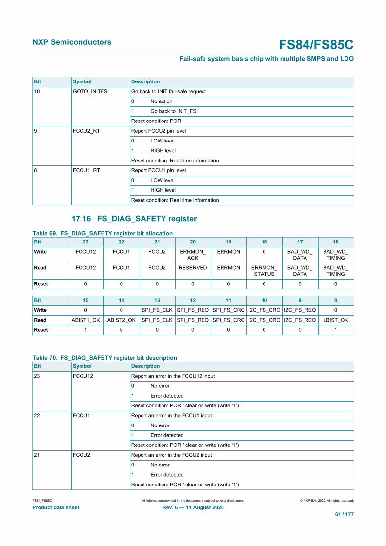
NXP Semiconductors FS84/FS85CFail-safe system basis chip with multiple SMPS and LDO
FS84_FS85C All information provided in this document is subject to legal disclaimers. © NXP B.V. 2020. All rights reserved.
Product data sheet Rev. 6 — 11 August 202061 / 177
Bit Symbol Description
Go back to INIT fail-safe request
0 No action
1 Go back to INIT_FS
10 GOTO_INITFS
Reset condition: POR
Report FCCU2 pin level
0 LOW level
1 HIGH level
9 FCCU2_RT
Reset condition: Real time information
Report FCCU1 pin level
0 LOW level
1 HIGH level
8 FCCU1_RT
Reset condition: Real time information
17.16 FS_DIAG_SAFETY register
Table 69. FS_DIAG_SAFETY register bit allocationBit 23 22 21 20 19 18 17 16
Write FCCU12 FCCU1 FCCU2 ERRMON_ACK
ERRMON 0 BAD_WD_DATA
BAD_WD_TIMING
Read FCCU12 FCCU1 FCCU2 RESERVED ERRMON ERRMON_STATUS
BAD_WD_DATA
BAD_WD_TIMING
Reset 0 0 0 0 0 0 0 0
Bit 15 14 13 12 11 10 9 8
Write 0 0 SPI_FS_CLK SPI_FS_REQ SPI_FS_CRC I2C_FS_CRC I2C_FS_REQ 0
Read ABIST1_OK ABIST2_OK SPI_FS_CLK SPI_FS_REQ SPI_FS_CRC I2C_FS_CRC I2C_FS_REQ LBIST_OK
Reset 1 0 0 0 0 0 0 1
Table 70. FS_DIAG_SAFETY register bit descriptionBit Symbol Description
Report an error in the FCCU12 input
0 No error
1 Error detected
23 FCCU12
Reset condition: POR / clear on write (write ‘1’)
Report an error in the FCCU1 input
0 No error
1 Error detected
22 FCCU1
Reset condition: POR / clear on write (write ‘1’)
Report an error in the FCCU2 input
0 No error
1 Error detected
21 FCCU2
Reset condition: POR / clear on write (write ‘1’)
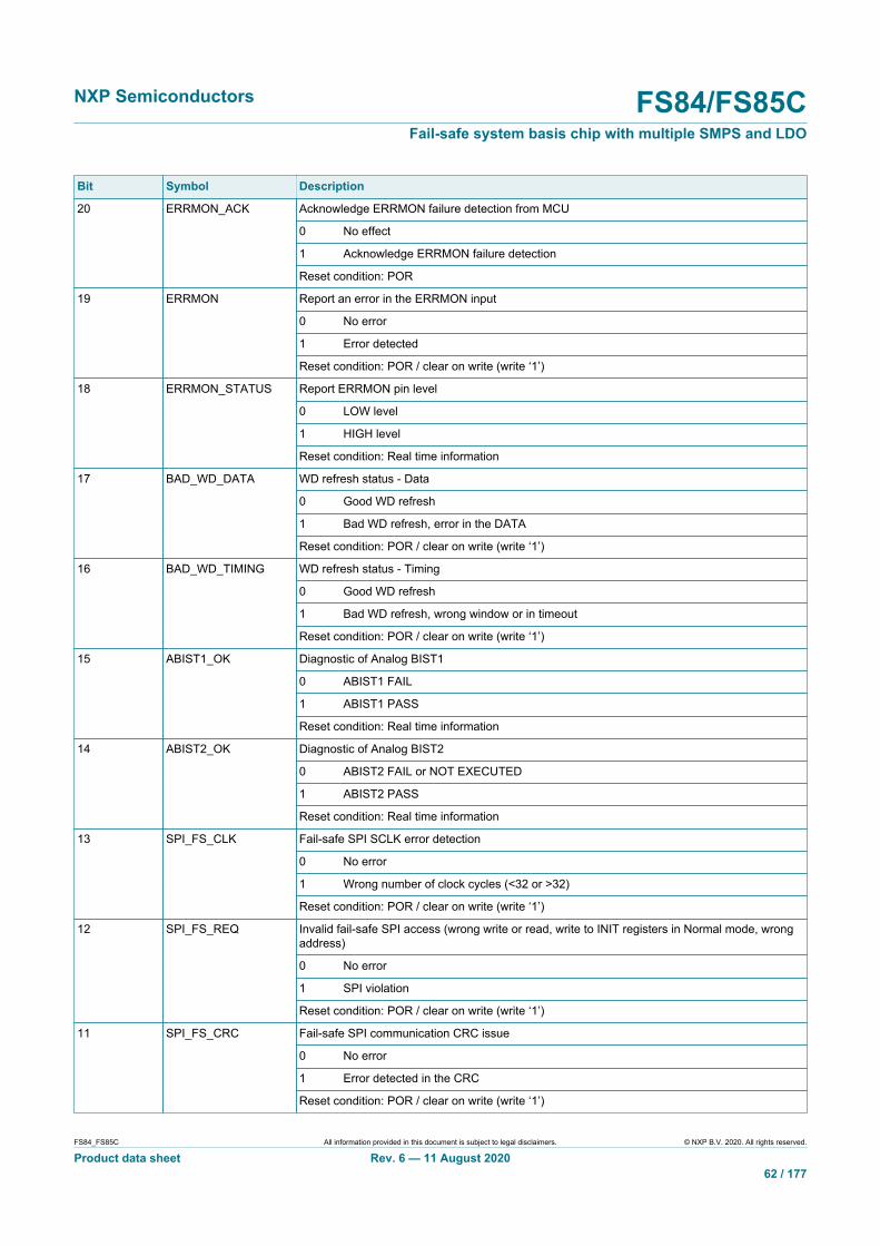
NXP Semiconductors FS84/FS85CFail-safe system basis chip with multiple SMPS and LDO
FS84_FS85C All information provided in this document is subject to legal disclaimers. © NXP B.V. 2020. All rights reserved.
Product data sheet Rev. 6 — 11 August 202062 / 177
Bit Symbol Description
Acknowledge ERRMON failure detection from MCU
0 No effect
1 Acknowledge ERRMON failure detection
20 ERRMON_ACK
Reset condition: POR
Report an error in the ERRMON input
0 No error
1 Error detected
19 ERRMON
Reset condition: POR / clear on write (write ‘1’)
Report ERRMON pin level
0 LOW level
1 HIGH level
18 ERRMON_STATUS
Reset condition: Real time information
WD refresh status - Data
0 Good WD refresh
1 Bad WD refresh, error in the DATA
17 BAD_WD_DATA
Reset condition: POR / clear on write (write ‘1’)
WD refresh status - Timing
0 Good WD refresh
1 Bad WD refresh, wrong window or in timeout
16 BAD_WD_TIMING
Reset condition: POR / clear on write (write ‘1’)
Diagnostic of Analog BIST1
0 ABIST1 FAIL
1 ABIST1 PASS
15 ABIST1_OK
Reset condition: Real time information
Diagnostic of Analog BIST2
0 ABIST2 FAIL or NOT EXECUTED
1 ABIST2 PASS
14 ABIST2_OK
Reset condition: Real time information
Fail-safe SPI SCLK error detection
0 No error
1 Wrong number of clock cycles (<32 or >32)
13 SPI_FS_CLK
Reset condition: POR / clear on write (write ‘1’)
Invalid fail-safe SPI access (wrong write or read, write to INIT registers in Normal mode, wrongaddress)
0 No error
1 SPI violation
12 SPI_FS_REQ
Reset condition: POR / clear on write (write ‘1’)
Fail-safe SPI communication CRC issue
0 No error
1 Error detected in the CRC
11 SPI_FS_CRC
Reset condition: POR / clear on write (write ‘1’)

NXP Semiconductors FS84/FS85CFail-safe system basis chip with multiple SMPS and LDO
FS84_FS85C All information provided in this document is subject to legal disclaimers. © NXP B.V. 2020. All rights reserved.
Product data sheet Rev. 6 — 11 August 202063 / 177
Bit Symbol Description
Fail-safe I2C communication CRC issue
0 No error
1 Error detected in the CRC
10 I2C_FS_CRC
Reset condition: POR / clear on write (write ‘1’)
Invalid fail-safe I2C access (wrong write or read, write to INIT registers in normal mode, wrongaddress)
0 No error
1 I2C violation
9 I2C_FS_REQ
Reset condition: POR / clear on write (write ‘1’)
Diagnostic of Logical BIST
0 LBIST FAIL
1 LBIST PASS
8 LBIST_OK
Reset condition: Real time information
17.17 FS_INTB_MASK register
Table 71. FS_INTB_MASK register bit allocationBit 23 22 21 20 19 18 17 16
Write 0 0 0 0 0 0 INT_INH_VMON4_OV_UV
INT_INH_VMON3_OV_UV
Read RESERVED RESERVED RESERVED RESERVED RESERVED RESERVED INT_INH_VMON4_OV_UV
INT_INH_VMON4_OV_UV
Reset 0 0 0 0 0 0 0 0
Bit 15 14 13 12 11 10 9 8
Write INT_INH_VMON2_OV_UV
INT_INH_VMON1_OV_UV
INT_INH_VDDIO_OV_UV
INT_INH_VCOREMON_
OV_UV
INT_INH_BAD_WD_REFRESH
INT_INH_ERRMON
INT_INH_FCCU2
INT_INH_FCCU1
Read INT_INH_VMON2_OV_UV
INT_INH_VMON1_OV_UV
INT_INH_VDDIO_OV_UV
INT_INH_VCOREMON_
OV_UV
INT_INH_BAD_WD_REFRESH
INT_INH_ERRMON
INT_INH_FCCU2
INT_INH_FCCU1
Reset 0 0 0 0 0 0 0 0
Table 72. FS_INTB_MASK register bit descriptionBit Symbol Description
Inhibit INTERRUPT on VMON4 OV and UV event
0 Interruption NOT MASKED
1 Interruption MASKED
17 INT_INH_VMON4_OV_UV
Reset condition: POR
Inhibit INTERRUPT on VMON3 OV and UV event
0 Interruption NOT MASKED
1 Interruption MASKED
16 INT_INH_VMON3_OV_UV
Reset condition: POR
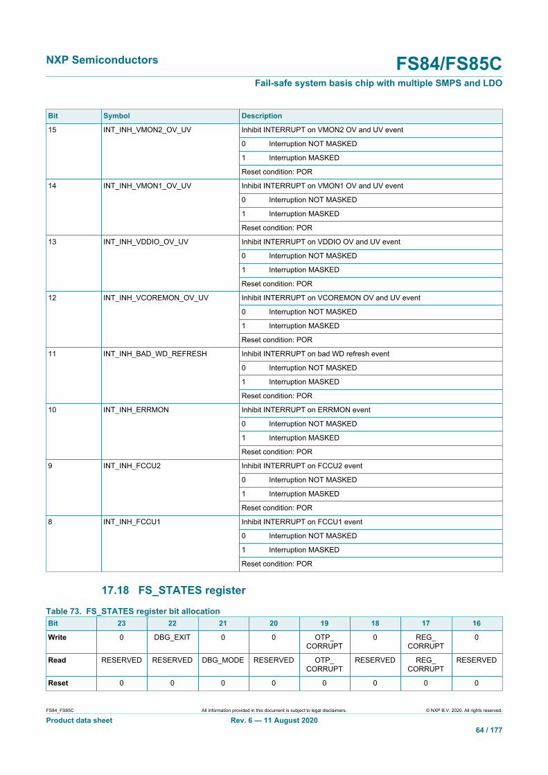
NXP Semiconductors FS84/FS85CFail-safe system basis chip with multiple SMPS and LDO
FS84_FS85C All information provided in this document is subject to legal disclaimers. © NXP B.V. 2020. All rights reserved.
Product data sheet Rev. 6 — 11 August 202064 / 177
Bit Symbol Description
Inhibit INTERRUPT on VMON2 OV and UV event
0 Interruption NOT MASKED
1 Interruption MASKED
15 INT_INH_VMON2_OV_UV
Reset condition: POR
Inhibit INTERRUPT on VMON1 OV and UV event
0 Interruption NOT MASKED
1 Interruption MASKED
14 INT_INH_VMON1_OV_UV
Reset condition: POR
Inhibit INTERRUPT on VDDIO OV and UV event
0 Interruption NOT MASKED
1 Interruption MASKED
13 INT_INH_VDDIO_OV_UV
Reset condition: POR
Inhibit INTERRUPT on VCOREMON OV and UV event
0 Interruption NOT MASKED
1 Interruption MASKED
12 INT_INH_VCOREMON_OV_UV
Reset condition: POR
Inhibit INTERRUPT on bad WD refresh event
0 Interruption NOT MASKED
1 Interruption MASKED
11 INT_INH_BAD_WD_REFRESH
Reset condition: POR
Inhibit INTERRUPT on ERRMON event
0 Interruption NOT MASKED
1 Interruption MASKED
10 INT_INH_ERRMON
Reset condition: POR
Inhibit INTERRUPT on FCCU2 event
0 Interruption NOT MASKED
1 Interruption MASKED
9 INT_INH_FCCU2
Reset condition: POR
Inhibit INTERRUPT on FCCU1 event
0 Interruption NOT MASKED
1 Interruption MASKED
8 INT_INH_FCCU1
Reset condition: POR
17.18 FS_STATES register
Table 73. FS_STATES register bit allocationBit 23 22 21 20 19 18 17 16
Write 0 DBG_EXIT 0 0 OTP_CORRUPT
0 REG_CORRUPT
0
Read RESERVED RESERVED DBG_MODE RESERVED OTP_CORRUPT
RESERVED REG_CORRUPT
RESERVED
Reset 0 0 0 0 0 0 0 0
NXP Semiconductors FS84/FS85CFail-safe system basis chip with multiple SMPS and LDO
FS84_FS85C All information provided in this document is subject to legal disclaimers. © NXP B.V. 2020. All rights reserved.
Product data sheet Rev. 6 — 11 August 202065 / 177
Bit 15 14 13 12 11 10 9 8
Write 0 0 0 0 0 0 0 0
Read RESERVED RESERVED RESERVED FSM_STATE |4:0]
Reset 0 0 0 0 0 1 1 0
Table 74. FS_STATES register bit descriptionBit Symbol Description
Leave DEBUG mode
0 No action
1 Leave DEBUG mode
22 DBG_EXIT
Reset condition: POR
DEBUG mode status
0 NOT in DEBUG mode
1 In DEBUG mode
21 DBG_MODE
Reset condition: Real time information
OTP bits corruption detection (5 ms cyclic check)
0 No error
1 OTP CRC error detected
19 OTP_CORRUPT
Reset condition: POR / clear on write (write ‘1’)
INIT register corruption detection (real time comparison)
0 No error
1 INIT register content error detected (mismatch between FS_I_Register / FS_I_NOT_Register)
167
REG_CORRUPT
Reset condition: POR / clear on write (write ‘1’)
Report fail-safe state machine current state
0 0110 INIT_FS
0 0111 WAIT_ABIST2
0 1000 ABIST2
0 1001 ASSERT_FS0B
0 1010 NORMAL _FS
12 to 8 FSM_STATE[3:0]
Reset condition: Real time information
NXP Semiconductors FS84/FS85CFail-safe system basis chip with multiple SMPS and LDO
FS84_FS85C All information provided in this document is subject to legal disclaimers. © NXP B.V. 2020. All rights reserved.
Product data sheet Rev. 6 — 11 August 202066 / 177
18 OTP bits description
18.1 Main OTP Overview
Table 75. Main OTP_REGISTERSName [1] Address BIT7 BIT6 BIT5 BIT4 BIT3 BIT2 BIT1 BIT0
OTP_CFG_VPRE_1 14 0 0 VPREV[5:0]
OTP_CFG_VPRE_2 15 0 0 VPRESC[5:0]
OTP_CFG_VPRE_3 16 VPREILIM[1:0] 1 0 1 1 VPRESRHS[1:0]
OTP_CFG_BOOST_1 17 0 0 VPRE_MODE 0 VBSTV[3:0]
OTP_CFG_BOOST_2 18 BOOSTEN VBSTTONTIME[1:0] VBSTSC[4:0]
OTP_CFG_BOOST_3 19 0 0 0 0 0 1 VBSTSR[1:0]
OTP_CFG_BUCK1_1 1A VB1V[7:0]
OTP_CFG_BUCK1_2 1B 0 0 0 VB1INDOPT[1:0] VB1SWILIM[1:0] VB12MULTIPH
OTP_CFG_BUCK2_1 1C VB2V[7:0]
OTP_CFG_BUCK2_2 1D 0 VB2INDOPT[1:0] BUCK2EN VB2SWILIM[1:0] 0 0
OTP_CFG_BUCK3_1 1E BUCK3EN VB3INDOPT[1:0] VB3V[4:0]
OTP_CFG_BUCK3_2 1F VB2GMCOMP[2:0] VB1GMCOMP[2:0] VB3SWILIM[1:0]
OTP_CFG_LDO 20 LDO2ILIM LDO2V[2:0] LDO1ILIM LDO1V[2:0]
OTP_CFG_SEQ_1 21 0 0 VB2S[2:0] VB1S[2:0]
OTP_CFG_SEQ_2 22 0 0 LDO2S[2:0] LDO1S[2:0]
OTP_CFG_SEQ_3 23 DVS_BUCK12[1:0] DVS_BUCK3[1:0] Tslot VB3S[2:0]
OTP_CFG_CLOCK_1 24 0 0 VPRE_ph[2:0] 1 0 0
OTP_CFG_CLOCK_2 25 0 0 BUCK1_ph[2:0] VBST_ph[2:0]
OTP_CFG_CLOCK_3 26 0 0 BUCK3_ph[2:0] BUCK2_ph[2:0]
OTP_CFG_CLOCK_4 27 BUCK3_clk_sel
BUCK2_clk_sel
BUCK1_clk_sel
VBST_clk_sel VPRE_clk_sel PLL_sel 0 1
OTP_CFG_SM_1 28 0 0 conf_TSD[5:0]
OTP_CFG_SM_2 29 0 0 0 VPRE_off_dly Autoretry_infinite
Autoretry_en PSYNC_CFG PSYNC_EN
OTP_CFG_VSUP_UV 2A 0 0 0 0 0 0 0 VSUPCFG
OTP_CFG_I2C 2B 0 0 0 0 M_I2CDEVADDR[3:0]
OTP_CFG_OV 2C 0 0 0 0 0 VDDIO_REG_ASSIGN[2:0]
OTP_CFG_DEVID 2D DeviceID[7:0]
[1] Regulator behavior in case of TSD, VPRE and VBOOST slew rate parameters in bold can be changed later by SPI/I2C.
18.2 Main OTP bit description
Table 76. Main OTP bit descriptionAddress Register Bit Symbol Value Description
VPRE output voltage
0 01111 3.3 V
010100 3.8 V
0 10111 4.1 V
14 OTP_CFG_VPRE_1 5 to 0 VPREV[5:0]
1 00000 5.0 V

NXP Semiconductors FS84/FS85CFail-safe system basis chip with multiple SMPS and LDO
FS84_FS85C All information provided in this document is subject to legal disclaimers. © NXP B.V. 2020. All rights reserved.
Product data sheet Rev. 6 — 11 August 202067 / 177
Address Register Bit Symbol Value Description
VPRE slope compensation
000100 40 mV/µs
000101 50 mV/µs
0 00110 60 mV/μs
0 00111 70 mV/μs
001000 80 mV/µs
001001 90 mV/µs
0 01010 100 mV/μs
0 01110 140 mV/μs
0 10001 170 mV/μs
0 10100 200 mV/μs
15 OTP_CFG_VPRE_2 5 to 0 VPRESC[5:0]
0 11000 240 mV/μs
VPRE current limitation threshold
00 50 mV
01 80 mV
10 120 mV
7 to 6 VPREILIM[1:0]
11 150 mV
VPRE high-side slew rate control
00 PU/PD/130 mA
01 PU/PD/260 mA
10 PU/PD/520 mA
16 OTP_CFG_VPRE_3
1 to 0 VPRESRHS[1:0]
11 PU/PD/900 mA
VPRE mode (PWM , APS)
0 Force PWM for 455 kHz setting
5 VPRE_MODE
1 Automatic Pulse Skipping (APS) for 2.2MHzsetting
VBOOST output voltage
0110 5.0 V
17 OTP_CFG_BOOST_1
3 to 0 VBSTV[3:0]
1101 5.74 V
BOOST enable
0 Disabled
7 BOOSTEN
1 Enabled
BOOST minimum ON time
00 60 ns
6 to 5 VBSTTONTIME[1:0]
01 50 ns
VBOOST slope compensation
0 0110 160 mV/μs
0 1100 125 mV/μs
18 OTP_CFG_BOOST_2
4 to 0 VBSTSC[4:0]
0 1110 79 mV/μs
VBOOST low-side slew rate control
10 300 V/μs
19 OTP_CFG_BOOST_3 1 to 0 VBSTSR[1:0]
11 500 V/μs
NXP Semiconductors FS84/FS85CFail-safe system basis chip with multiple SMPS and LDO
FS84_FS85C All information provided in this document is subject to legal disclaimers. © NXP B.V. 2020. All rights reserved.
Product data sheet Rev. 6 — 11 August 202068 / 177
Address Register Bit Symbol Value Description
VBUCK1 output voltage
0100 0000 0.8 V
0100 0100 0.825 V
0101 0000 0.9 V
0101 1000 0.95 V
0110 0000 1.0 V
01100100 1.025 V
0110 0101 1.03125 V
0111 0000 1.1 V
1000 0000 1.2 V
1000 1000 1.25 V
1001 0000 1.3 V
1001 1000 1.35 V
1010 0000 1.4 V
1011 0000 1.5 V
1A OTP_CFG_BUCK1_1 7 to 0 VB1V[7:0]
1011 0001 1.8 V
BUCK1 inductor selection
00 1 μH
01 0.47 μH
4 to 3 VB1INDOPT[1:0]
10 1.5 μH
BUCK1 current limitation
01 2.6 A
2 to 1 VB1SWILIM[1:0]
11 4.5 A
VBUCK1 and VBUCK2 multiphase operationenable
0 Disabled
1B OTP_CFG_BUCK1_2
0 VB12MULTIPH
1 Enabled
VBUCK2 output voltage
0100 0000 0.8 V
0100 0100 0.825 V
0101 0000 0.9 V
0101 1000 0.95 V
0110 0000 1.0 V
01100100 1.025 V
0110 0101 1.03125 V
0111 0000 1.1 V
1000 0000 1.2 V
1000 1000 1.25 V
1001 0000 1.3 V
1001 1000 1.35 V
1010 0000 1.4 V
1011 0000 1.5 V
1C OTP_CFG_BUCK2_1 7 to 0 VB2V[7:0]
1011 0001 1.8 V
NXP Semiconductors FS84/FS85CFail-safe system basis chip with multiple SMPS and LDO
FS84_FS85C All information provided in this document is subject to legal disclaimers. © NXP B.V. 2020. All rights reserved.
Product data sheet Rev. 6 — 11 August 202069 / 177
Address Register Bit Symbol Value Description
BUCK2 inductor selection
00 1 μH
01 0.47 μH
6 to 5 VB2INDOPT[1:0]
10 1.5 μH
BUCK2 enable
0 Disabled
4 BUCK2EN
1 Enabled
BUCK2 current limitation
01 2.6 A
1D OTP_CFG_BUCK2_2
3 to 2 VB2SWILIM[1:0]
11 4.5 A
BUCK3 enable
0 Disabled
7 BUCK3EN
1 Enabled
BUCK3 inductor selection
00 1 μH
01 0.47 μH
6 to 5 VB3INDOPT[1:0]
10 1.5 μH
VBUCK3 output voltage
0 0000 1.0 V
0 0001 1.1 V
0 0010 1.2 V
0 0011 1.25 V
0 0100 1.3 V
0 0101 1.35 V
0 0110 1.5 V
0 0111 1.6 V
0 1000 1.8 V
0 1110 2.3 V
1 0000 2.5 V
1 0001 2.8 V
1E OTP_CFG_BUCK3_1
4 to 0 VB3V[4:0]
1 0101 3.3 V
NXP Semiconductors FS84/FS85CFail-safe system basis chip with multiple SMPS and LDO
FS84_FS85C All information provided in this document is subject to legal disclaimers. © NXP B.V. 2020. All rights reserved.
Product data sheet Rev. 6 — 11 August 202070 / 177
Address Register Bit Symbol Value Description
BUCK2 compensation network
001 16.25 GM
010 32.5 GM
011 48.75 GM
100 65 GM
101 81.25 GM
7 to 5 VB2GMCOMP[2:0]
110 97.5 GM
BUCK1 compensation network
001 16.25 GM
010 32.5 GM
011 48.75 GM
100 65 GM
101 81.25 GM
4 to 2 VB1GMCOMP[2:0]
110 97.5 GM
BUCK3 current limitation
01 2.6 A
1F OTP_CFG_BUCK3_2
1 to 0 VB3SWILIM[1:0]
11 4.5 A
VLDO2 current limitation
0 400 mA
7 LDO2ILIM
1 150 mA
VLDO2 output voltage
000 1.1 V
001 1.2 V
010 1.6 V
011 1.8 V
100 2.5 V
101 2.8 V
110 3.3 V
6 to 4 LDO2V[2:0]
111 5.0 V
VLDO1 current limitation
0 400 mA
3 LDO1ILIM
1 150 mA
VLDO1 output voltage
000 1.1 V
001 1.2 V
010 1.6 V
011 1.8 V
100 2.5 V
101 2.8 V
110 3.3 V
20 OTP_CFG_LDO
2 to 0 LDO1V[2:0]
111 5.0 V
NXP Semiconductors FS84/FS85CFail-safe system basis chip with multiple SMPS and LDO
FS84_FS85C All information provided in this document is subject to legal disclaimers. © NXP B.V. 2020. All rights reserved.
Product data sheet Rev. 6 — 11 August 202071 / 177
Address Register Bit Symbol Value Description
BUCK2 sequencing slot
000 Regulator start and stop in Slot 0
001 Regulator start and stop in Slot 1
010 Regulator start and stop in Slot 2
011 Regulator start and stop in Slot 3
100 Regulator start and stop in Slot 4
101 Regulator start and stop in Slot 5
110 Regulator start and stop in Slot 6
5 to 3 VB2S[2:0]
111 Regulator does not start (enabled by SPI)
BUCK1 sequencing slot
000 Regulator start and stop in Slot 0
001 Regulator start and stop in Slot 1
010 Regulator start and stop in Slot 2
011 Regulator start and stop in Slot 3
100 Regulator start and stop in Slot 4
101 Regulator start and stop in Slot 5
110 Regulator start and stop in Slot 6
21 OTP_CFG_SEQ_1
2 to 0 VB1S[2:0]
111 Regulator does not start (enabled by SPI)
LDO2 sequencing slot
000 Regulator start and stop in Slot 0
001 Regulator start and stop in Slot 1
010 Regulator start and Stop in Slot 2
011 Regulator start and stop in Slot 3
100 Regulator start and stop in Slot 4
101 Regulator start and stop in Slot 5
110 Regulator start and stop in Slot 6
5 to 3 LDO2S[2:0]
111 Regulator does not start (enabled by SPI)
LDO1 sequencing slot
000 Regulator start and stop in Slot 0
001 Regulator start and stop in Slot 1
010 Regulator start and stop in Slot 2
011 Regulator start and stop in Slot 3
100 Regulator start and stop in Slot 4
101 Regulator start and stop in Slot 5
110 Regulator start and stop in Slot 6
22 OTP_CFG_SEQ_2
2 to 0 LDO1S[2:0]
111 Regulator does not start (enabled by SPI)
BUCK1 and BUCK2 soft start/stop configurability
00 7.81 mV/µs
01 3.13 mV/µs
10 2.6 mV/µs
7 to 6 DVS_BUCK12[1:0]
11 2.23 mV/µs
BUCK3 soft start/stop configurability
00 10.41 mV/µs
01 3.47 mV/µs
10 2.6 mV/µs
23 OTP_CFG_SEQ_3
5 to 4 DVS_BUCK3[1:0]
11 2.08 mV/µs

NXP Semiconductors FS84/FS85CFail-safe system basis chip with multiple SMPS and LDO
FS84_FS85C All information provided in this document is subject to legal disclaimers. © NXP B.V. 2020. All rights reserved.
Product data sheet Rev. 6 — 11 August 202072 / 177
Address Register Bit Symbol Value Description
Power up/down slot duration
0 250 µs
3 Tslot
1 1 ms
BUCK3 sequencing slot
000 Regulator start and stop in Slot 0
001 Regulator start and stop in Slot 1
010 Regulator start and Stop in Slot 2
011 Regulator start and stop in Slot 3
100 Regulator start and stop in Slot 4
101 Regulator start and stop in Slot 5
110 Regulator start and stop in Slot 6
2 to 0 VB3S[2:0]
111 Regulator does not start (enabled by SPI)
VPRE phase (delay) selection
000 no delay
001 delay 1
010 delay 2
011 delay 3
100 delay 4
101 delay 5
110 delay 6
24 OTP_CFG_CLOCK_1 5 to 3 VPRE_ph[2:0]
111 delay 7
VBUCK1 phase (delay) selection
000 no delay
001 delay 1
010 delay 2
011 delay 3
100 delay 4
101 delay 5
110 delay 6
5 to 3 BUCK1_ph[2:0]
111 delay 7
VBOOST phase (delay) selection
000 no delay
001 delay 1
010 delay 2
011 delay 3
100 delay 4
101 delay 5
110 delay 6
25 OTP_CFG_CLOCK_2
2 to 0 VBST_ph[2:0]
111 delay 7
NXP Semiconductors FS84/FS85CFail-safe system basis chip with multiple SMPS and LDO
FS84_FS85C All information provided in this document is subject to legal disclaimers. © NXP B.V. 2020. All rights reserved.
Product data sheet Rev. 6 — 11 August 202073 / 177
Address Register Bit Symbol Value Description
VBUCK3 phase (delay) selection
000 no delay
001 delay 1
010 delay 2
011 delay 3
100 delay 4
101 delay 5
110 delay 6
5 to 3 BUCK3_ph[2:0]
111 delay 7
VBUCK2 phase (delay) selection
000 no delay
001 delay 1
010 delay 2
011 delay 3
100 delay 4
101 delay 5
110 delay 6
26 OTP_CFG_CLOCK_3
2 to 0 BUCK2_ph[2:0]
111 delay 7
BUCK3 clock selection7 BUCK3_clk_sel
0 CLK_DIV1 = 2.22 MHz
BUCK2 clock selection6 BUCK2_clk_sel
0 CLK_DIV1 = 2.22 MHz
BUCK1 clock selection5 BUCK1_clk_sel
0 CLK_DIV1 = 2.22 MHz
VBOOST clock selection4 VBST_clk_sel
0 CLK_DIV1 = 2.22 MHz
VPRE clock selection
0 CLK_DIV1 = 2.22 MHz
3 VPRE_clk_sel
1 CLK_DIV2 = 455 kHz
PLL enable
0 Disabled
27 OTP_CFG_CLOCK_4
2 PLL_sel
1 Enabled
NXP Semiconductors FS84/FS85CFail-safe system basis chip with multiple SMPS and LDO
FS84_FS85C All information provided in this document is subject to legal disclaimers. © NXP B.V. 2020. All rights reserved.
Product data sheet Rev. 6 — 11 August 202074 / 177
Address Register Bit Symbol Value Description
BOOST behavior in case of TSD
0 BOOST shutdown
conf_TSD[5]
1 BOOST shutdown + DFS
BUCK1 behavior in case of TSD
0 BUCK1 shutdown
conf_TSD[4]
1 BUCK1 shutdown + DFS
BUCK2 behavior in case of TSD
0 BUCK2 shutdown
conf_TSD[3]
1 BUCK2 shutdown + DFS
BUCK3 behavior in case of TSD
0 BUCK3 shutdown
conf_TSD[2]
1 BUCK3 Shutdown + DFS
LDO1 behavior in case of TSD
0 LDO1 shutdown
conf_TSD[1]
1 LDO1 shutdown + DFS
LDO2 behavior in case of TSD
0 LDO2 shutdown
28 OTP_CFG_SM_1 5 to 0
conf_TSD[0]
1 LDO2 shutdown + DFS
Delay to turn OFF VPRE at device power down
0 250 μs
4 VPRE_off_dly
1 32 ms
Deep fail-safe infinite autoretry enable
0 Disabled
3 Autoretry_infinite
1 Enabled
Deep fail-safe autoretry enable
0 Disabled
2 Autoretry_en
1 Enabled
Power up synchronization
0 2x FS85
1 PSYNC_CFG
1 1x FS85 and 1x ext. PMIC
Synchronization with two devices
0 Disabled
29 OTP_CFG_SM_2
0 PSYNC_EN
1 Enabled
VSUP undervoltage threshold configuration
0 4.9 V for Vpre < 4.5 V
2A OTP_CFG_VSUP_UV 0 VSUP_CFG
1 6.2 V for Vpre > 4.5 V
Device I2C address
0000 Address D0
… ...
2B OTP_CFG_I2C 3 to 0 M_I2CDEVADDR[3:0]
1111 Address D15

NXP Semiconductors FS84/FS85CFail-safe system basis chip with multiple SMPS and LDO
FS84_FS85C All information provided in this document is subject to legal disclaimers. © NXP B.V. 2020. All rights reserved.
Product data sheet Rev. 6 — 11 August 202075 / 177
Address Register Bit Symbol Value Description
Regulator assigned to VDDIO
000 External regulator
001 VPRE
010 LDO1
011 LDO2
100 BUCK3
101 External regulator
110 External regulator
2C OTP_CFG_OV 2 to 0 VDDIO_REG_ASSIGN[2:0]
111 External regulator
2D OTP_CFG_DEVID 7 to 0 DeviceID[7:0] Device ID
18.3 Fail-safe OTP Overview
Table 77. Fail-safe OTP_REGISTERSName Address BIT7 BIT6 BIT5 BIT4 BIT3 BIT2 BIT1 BIT0
OTP_CFG_UVOV_1 0A VCORE_V[7:0]
OTP_CFG_UVOV_2 0B VDDIOOVTH[3:0] VCOREOVTH[3:0]
OTP_CFG_UVOV_3 0C 0 0 VDDIO_V VCORE_SVS_CLAMP[4:0]
OTP_CFG_UVOV_4 0D VMON2OVTH[3:0] VMON1OVTH[3:0]
OTP_CFG_UVOV_5 0E VMON4OVTH[3:0] VMON3OVTH[3:0]
OTP_CFG_UVOV_6 0F VDDIOUVTH[3:0] VCOREUVTH[3:0]
OTP_CFG_UVOV_7 10 VMON2UVTH[3:0] VMON1UVTH[3:0]
OTP_CFG_UVOV_8 11 VMON4UVTH[3:0] VMON3UVTH[3:0]
OTP_CFG_PGOOD 12 0 PGOOD_RSTB
PGOOD_VMON4
PGOOD_VMON3
PGOOD_VMON2
PGOOD_VMON1
PGOOD_VDDIO
PGOOD_VCORE
OTP_CFG_ABIST1 13 0 0 ABIST1_VMON4
ABIST1_VMON3
ABIST1_VMON2
ABIST1_VMON1
ABIST1_VDDIO
ABIST1_VCORE
OTP_CFG_ASIL 14 WD_DIS WD_Selection ERRMON_EN FCCU_EN VMON4_EN VMON3_EN VMON2_EN VMON1_EN
OTP_CFG_I2C 15 0 0 0 FLT_RECOVERY_
EN
FS_I2CDEVADDR[3:0]
OTP_CFG_DGLT_DUR_1 16 0 0 VCORE_UV_DGLT[1:0] VCORE_OV_DGLT
VDDIO_UV_DGLT[1:0] VDDIO_OV_DGLT
OTP_CFG_DGLT_DUR_2 17 0 0 0 0 0 VMONx_UV_DGLT[1:0] VMONx_OV_DGLT
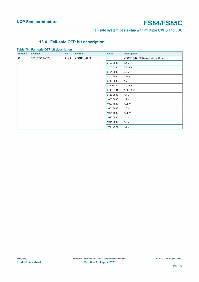
NXP Semiconductors FS84/FS85CFail-safe system basis chip with multiple SMPS and LDO
FS84_FS85C All information provided in this document is subject to legal disclaimers. © NXP B.V. 2020. All rights reserved.
Product data sheet Rev. 6 — 11 August 202076 / 177
18.4 Fail-safe OTP bit description
Table 78. Fail-safe OTP bit descriptionAddress Register Bit Symbol Value Description
VCORE (VBUCK1) monitoring voltage
0100 0000 0.8 V
0100 0100 0.825 V
0101 0000 0.9 V
0101 1000 0.95 V
0110 0000 1 V
01100100 1.025 V
0110 0101 1.03125 V
0110 0000 1.1 V
1000 0000 1.2 V
1000 1000 1.25 V
1001 0000 1.3 V
1001 1000 1.35 V
1010 0000 1.4 V
1011 0000 1.5 V
0A OTP_CFG_UVOV_1 7 to 0 VCORE_V[7:0]
1011 0001 1.8 V
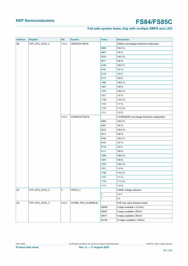
NXP Semiconductors FS84/FS85CFail-safe system basis chip with multiple SMPS and LDO
FS84_FS85C All information provided in this document is subject to legal disclaimers. © NXP B.V. 2020. All rights reserved.
Product data sheet Rev. 6 — 11 August 202077 / 177
Address Register Bit Symbol Value Description
VDDIO overvoltage threshold configuration
0000 104.5 %
0001 105 %
0010 105.5 %
0011 106 %
0100 106.5 %
0101 107 %
0110 107.5
0111 108 %
1000 108.5 %
1001 109 %
1010 109.5 %
1011 110 %
1100 110.5 %
1101 111 %
1110 111.5 %
7 to 4 VDDIOOVTH[3:0]
1111 112 %
VCOREMON overvoltage threshold configuration
0000 104.5 %
0001 105 %
0010 105.5 %
0011 106 %
0100 106.5 %
0101 107 %
0110 107.5
0111 108 %
1000 108.5 %
1001 109 %
1010 109.5 %
1011 110 %
1100 110.5 %
1101 111 %
1110 111.5 %
0B OTP_CFG_UVOV_2
3 to 0 VCOREOVTH[3:0]
1111 112 %
VDDIO voltage selection
0 3.3 V
0C OTP_CFG_UVOV_3 5 VDDIO_V
1 5 V
SVS max value allowed (mask)
00000 2 steps available (-12.5mV)
00001 4 steps available (-25mV)
00011 8 steps available (-50mV)
0C OTP_CFG_UVOV_3 4 to 0 VCORE_SVS_CLAMP[4:0]
00100 16 steps available (-100mV)

NXP Semiconductors FS84/FS85CFail-safe system basis chip with multiple SMPS and LDO
FS84_FS85C All information provided in this document is subject to legal disclaimers. © NXP B.V. 2020. All rights reserved.
Product data sheet Rev. 6 — 11 August 202078 / 177
Address Register Bit Symbol Value Description
VMON2 overvoltage threshold configuration
0000 104.5 %
0001 105 %
0010 105.5 %
0011 106 %
0100 106.5 %
0101 107 %
0110 107.5
0111 108 %
1000 108.5 %
1001 109 %
1010 109.5 %
1011 110 %
1100 110.5 %
1101 111 %
1110 111.5 %
7 to 4 VMON2OVTH[3:0]
1111 112 %
VMON1 overvoltage threshold configuration
0000 104.5 %
0001 105 %
0010 105.5 %
0011 106 %
0100 106.5 %
0101 107 %
0110 107.5
0111 108 %
1000 108.5 %
1001 109 %
1010 109.5 %
1011 110 %
1100 110.5 %
1101 111 %
1110 111.5 %
0D OTP_CFG_UVOV_4
3 to 0 VMON1OVTH[3:0]
1111 112 %

NXP Semiconductors FS84/FS85CFail-safe system basis chip with multiple SMPS and LDO
FS84_FS85C All information provided in this document is subject to legal disclaimers. © NXP B.V. 2020. All rights reserved.
Product data sheet Rev. 6 — 11 August 202079 / 177
Address Register Bit Symbol Value Description
VMON4 overvoltage threshold configuration
0000 104.5 %
0001 105 %
0010 105.5 %
0011 106 %
0100 106.5 %
0101 107 %
0110 107.5
0111 108 %
1000 108.5 %
1001 109 %
1010 109.5 %
1011 110 %
1100 110.5 %
1101 111 %
1110 111.5 %
7 to 4 VMON4OVTH[3:0]
1111 112 %
VMON3 overvoltage threshold configuration
0000 104.5 %
0001 105 %
0010 105.5 %
0011 106 %
0100 106.5 %
0101 107 %
0110 107.5
0111 108 %
1000 108.5 %
1001 109 %
1010 109.5 %
1011 110 %
1100 110.5 %
1101 111 %
1110 111.5 %
0E OTP_CFG_UVOV_5
3 to 0 VMON3OVTH[3:0]
1111 112 %

NXP Semiconductors FS84/FS85CFail-safe system basis chip with multiple SMPS and LDO
FS84_FS85C All information provided in this document is subject to legal disclaimers. © NXP B.V. 2020. All rights reserved.
Product data sheet Rev. 6 — 11 August 202080 / 177
Address Register Bit Symbol Value Description
VDDIO undervoltage threshold configuration
0000 95.5 %
0001 95 %
0010 94.5 %
0011 94 %
0100 93.5 %
0101 93 %
0110 92.5 %
0111 92 %
1000 91.5 %
1001 91 %
1010 90.5 %
1011 90 %
1100 89.5 %
1101 89 %
1110 88.5 %
7 to 4 VDDIOUVTH[3:0]
1111 88 %
VCOREMON undervoltage threshold configuration
0000 95.5 %
0001 95 %
0010 94.5 %
0011 94 %
0100 93.5 %
0101 93 %
0110 92.5 %
0111 92 %
1000 91.5 %
1001 91 %
1010 90.5 %
1011 90 %
1100 89.5 %
1101 89 %
1110 88.5 %
0F OTP_CFG_UVOV_6
3 to 0 VCOREUVTH[3:0]
1111 88 %

NXP Semiconductors FS84/FS85CFail-safe system basis chip with multiple SMPS and LDO
FS84_FS85C All information provided in this document is subject to legal disclaimers. © NXP B.V. 2020. All rights reserved.
Product data sheet Rev. 6 — 11 August 202081 / 177
Address Register Bit Symbol Value Description
VMON2 undervoltage threshold configuration
0000 95.5 %
0001 95 %
0010 94.5 %
0011 94 %
0100 93.5 %
0101 93 %
0110 92.5 %
0111 92 %
1000 91.5 %
1001 91 %
1010 90.5 %
1011 90 %
1100 89.5 %
1101 89 %
1110 88.5 %
7 to 4 VMON2UVTH[3:0]
1111 88 %
VMON1 undervoltage threshold configuration
0000 95.5 %
0001 95 %
0010 94.5 %
0011 94 %
0100 93.5 %
0101 93 %
0110 92.5 %
0111 92 %
1000 91.5 %
1001 91 %
1010 90.5 %
1011 90 %
1100 89.5 %
1101 89 %
1110 88.5 %
10 OTP_CFG_UVOV_7
3 to 0 VMON1UVTH[3:0]
1111 88 %
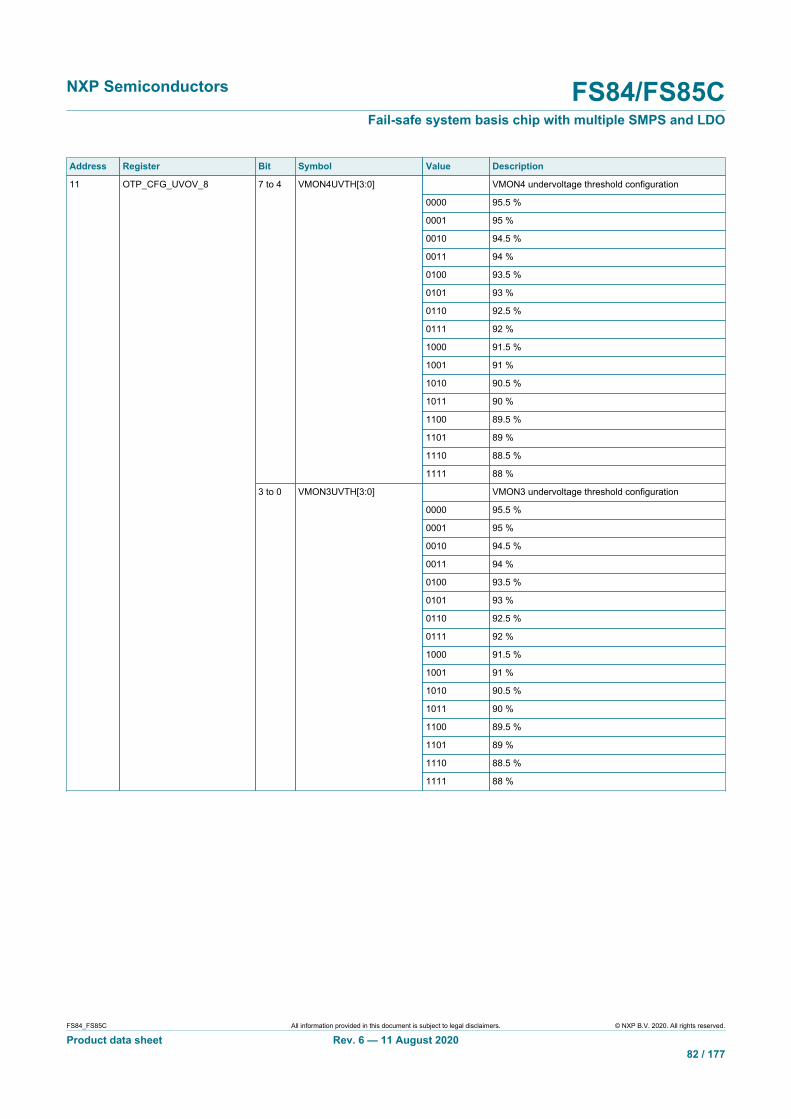
NXP Semiconductors FS84/FS85CFail-safe system basis chip with multiple SMPS and LDO
FS84_FS85C All information provided in this document is subject to legal disclaimers. © NXP B.V. 2020. All rights reserved.
Product data sheet Rev. 6 — 11 August 202082 / 177
Address Register Bit Symbol Value Description
VMON4 undervoltage threshold configuration
0000 95.5 %
0001 95 %
0010 94.5 %
0011 94 %
0100 93.5 %
0101 93 %
0110 92.5 %
0111 92 %
1000 91.5 %
1001 91 %
1010 90.5 %
1011 90 %
1100 89.5 %
1101 89 %
1110 88.5 %
7 to 4 VMON4UVTH[3:0]
1111 88 %
VMON3 undervoltage threshold configuration
0000 95.5 %
0001 95 %
0010 94.5 %
0011 94 %
0100 93.5 %
0101 93 %
0110 92.5 %
0111 92 %
1000 91.5 %
1001 91 %
1010 90.5 %
1011 90 %
1100 89.5 %
1101 89 %
1110 88.5 %
11 OTP_CFG_UVOV_8
3 to 0 VMON3UVTH[3:0]
1111 88 %
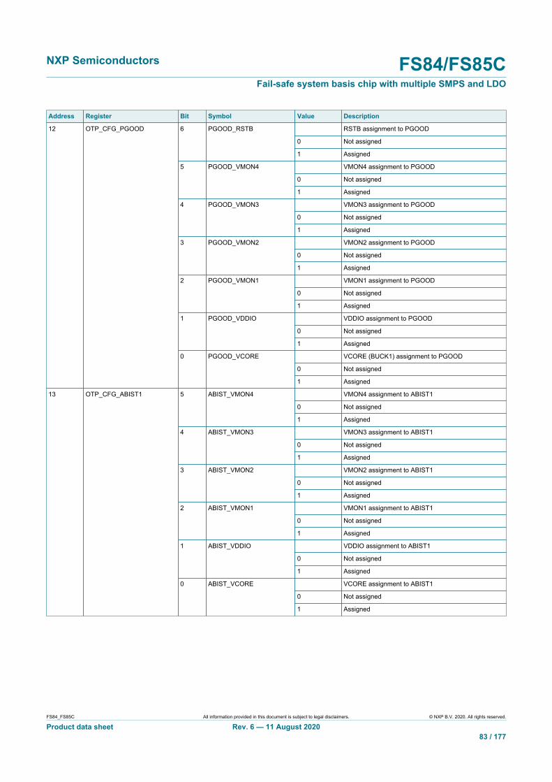
NXP Semiconductors FS84/FS85CFail-safe system basis chip with multiple SMPS and LDO
FS84_FS85C All information provided in this document is subject to legal disclaimers. © NXP B.V. 2020. All rights reserved.
Product data sheet Rev. 6 — 11 August 202083 / 177
Address Register Bit Symbol Value Description
RSTB assignment to PGOOD
0 Not assigned
6 PGOOD_RSTB
1 Assigned
VMON4 assignment to PGOOD
0 Not assigned
5 PGOOD_VMON4
1 Assigned
VMON3 assignment to PGOOD
0 Not assigned
4 PGOOD_VMON3
1 Assigned
VMON2 assignment to PGOOD
0 Not assigned
3 PGOOD_VMON2
1 Assigned
VMON1 assignment to PGOOD
0 Not assigned
2 PGOOD_VMON1
1 Assigned
VDDIO assignment to PGOOD
0 Not assigned
1 PGOOD_VDDIO
1 Assigned
VCORE (BUCK1) assignment to PGOOD
0 Not assigned
12 OTP_CFG_PGOOD
0 PGOOD_VCORE
1 Assigned
VMON4 assignment to ABIST1
0 Not assigned
5 ABIST_VMON4
1 Assigned
VMON3 assignment to ABIST1
0 Not assigned
4 ABIST_VMON3
1 Assigned
VMON2 assignment to ABIST1
0 Not assigned
3 ABIST_VMON2
1 Assigned
VMON1 assignment to ABIST1
0 Not assigned
2 ABIST_VMON1
1 Assigned
VDDIO assignment to ABIST1
0 Not assigned
1 ABIST_VDDIO
1 Assigned
VCORE assignment to ABIST1
0 Not assigned
13 OTP_CFG_ABIST1
0 ABIST_VCORE
1 Assigned

NXP Semiconductors FS84/FS85CFail-safe system basis chip with multiple SMPS and LDO
FS84_FS85C All information provided in this document is subject to legal disclaimers. © NXP B.V. 2020. All rights reserved.
Product data sheet Rev. 6 — 11 August 202084 / 177
Address Register Bit Symbol Value Description
Watchdog monitoring enable
0 Enabled
7 WD_DIS
1 Disabled
Watchdog mode selection
0 Simple WD
6 WD_SELECTION
1 Challenger WD
ERRMON monitoring enable
0 Disabled
5 ERRMON_EN
1 Enabled
FCCU monitoring enable
0 Disabled
4 FCCU_EN
1 Enabled
VMON4 monitoring enable
0 Disabled
3 VMON4_EN
1 Enabled
VMON3 monitoring enable
0 Disabled
2 VMON3_EN
1 Enabled
VMON2 monitoring enable
0 Disabled
1 VMON2_EN
1 Enabled
VMON1 monitoring enable
0 Disabled
14 OTP_CFG_ASIL
0 VMON1_EN
1 Enabled
Fault recovery strategy enable
0 Disabled
4 FLT_RECOVERY_EN
1 Enabled
Device I2C address
0000 Address D0
… …
15 OTP_CFG_I2C
3 to 0 FS_I2CDEVADDR[3:0]
1111 Address D15
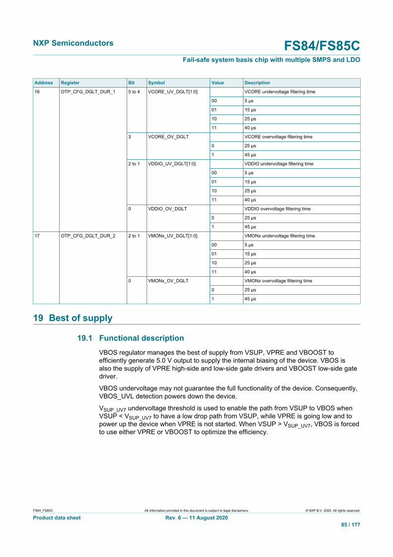
NXP Semiconductors FS84/FS85CFail-safe system basis chip with multiple SMPS and LDO
FS84_FS85C All information provided in this document is subject to legal disclaimers. © NXP B.V. 2020. All rights reserved.
Product data sheet Rev. 6 — 11 August 202085 / 177
Address Register Bit Symbol Value Description
VCORE undervoltage filtering time
00 5 μs
01 15 μs
10 25 μs
5 to 4 VCORE_UV_DGLT[1:0]
11 40 μs
VCORE overvoltage filtering time
0 25 μs
3 VCORE_OV_DGLT
1 45 μs
VDDIO undervoltage filtering time
00 5 μs
01 15 μs
10 25 μs
2 to 1 VDDIO_UV_DGLT[1:0]
11 40 μs
VDDIO overvoltage filtering time
0 25 μs
16 OTP_CFG_DGLT_DUR_1
0 VDDIO_OV_DGLT
1 45 μs
VMONx undervoltage filtering time
00 5 μs
01 15 μs
10 25 μs
2 to 1 VMONx_UV_DGLT[1:0]
11 40 μs
VMONx overvoltage filtering time
0 25 μs
17 OTP_CFG_DGLT_DUR_2
0 VMONx_OV_DGLT
1 45 μs
19 Best of supply
19.1 Functional descriptionVBOS regulator manages the best of supply from VSUP, VPRE and VBOOST toefficiently generate 5.0 V output to supply the internal biasing of the device. VBOS isalso the supply of VPRE high-side and low-side gate drivers and VBOOST low-side gatedriver.
VBOS undervoltage may not guarantee the full functionality of the device. Consequently,VBOS_UVL detection powers down the device.
VSUP_UV7 undervoltage threshold is used to enable the path from VSUP to VBOS whenVSUP < VSUP_UV7 to have a low drop path from VSUP, while VPRE is going low and topower up the device when VPRE is not started. When VSUP > VSUP_UV7, VBOS is forcedto use either VPRE or VBOOST to optimize the efficiency.

NXP Semiconductors FS84/FS85CFail-safe system basis chip with multiple SMPS and LDO
FS84_FS85C All information provided in this document is subject to legal disclaimers. © NXP B.V. 2020. All rights reserved.
Product data sheet Rev. 6 — 11 August 202086 / 177
19.2 Electrical characteristics
Table 79. Best of supply electrical characteristicsTA = –40 °C to 125 °C, unless otherwise specified. VSUP = VSUP_UVH to 36 V, unless otherwise specified. All voltagesreferenced to ground.
Symbol Parameter Min Typ Max Unit
Best of supply
VBOS Best of supply output voltage 3.3 5.0 5.25 V
VBOS_UVHVBOS undervoltage threshold high (VBOSrising) 4.1 — 4.5 V
VBOS_UVLVBOS undervoltage threshold low (VBOSfalling) 3.2 — 3.4 V
TBOS_UV VBOS_UVH and VBOS_UVL filtering time 6.0 10 15 μs
VBOS_POR VBOS power on reset threshold — — 2.5 V
TBOS_POR VBOS_POR filtering time 0.5 — 1.5 μs
IBOS Best of supply current capability — — 60 mA
Effective output capacitor 4.7 — 10 µFCOUT_BOS
Output decoupling capacitor 0.1 — µF
20 High voltage buck: VPRE
20.1 Functional descriptionVPRE block is a high voltage, synchronous, peak current mode buck controller. VPREis working with external logical level NMOS in force PWM mode at 455 kHz and inAutomatic Pulse Skipping (APS) mode at 2.22 MHz. The APS mode helps to maintainthe correct output voltage at high input voltage by skipping some turn ON cycles of theHS FET below the minimum duty cycle. VPRE input voltage is naturally limited to VSUP =LPI_DCR × IPRE + VPRE_UVL / DMAX with DMAX = 1 − (FPRE_SW × TPRE_OFF_MIN).
A bootstrap capacitor is required to supply the gate drive circuit of the high-sideNMOS. The output voltage is configurable by OTP from 3.3 V to 5.0 V, and theswitching frequency is configurable by OTP at 455 kHz for 12 V and 24 V transportationapplications or 2.22 MHz for 12 V automotive applications. The stability is ensured by anexternal Type 2 compensation network with slope compensation.
The output current is sensed via an external shunt in series with the inductor andthe maximum current capability is defined by the external components (NMOS gatecharge, inductor, shunt resistor), the gate driver current capability and the switchingfrequency. An overcurrent detection is implemented to protect the external MOSFETs.If an overcurrent is detected after the HS minimum TON time, the HS is turned OFF andwill be turned ON again at the next rising edge of the switching clock. The overcurrentinduces a duty cycle reduction that could lead to the output voltage gradually dropping,causing an undervoltage condition on VPRE and/or one of the cascaded regulators.
The maximum input voltage is 60 V and allows operation in 24 V truck applicationswithout external protection to sustain ISO 16750-2:2012 load dump pulse 5b. VPREmust be the input supply of the BOOST and BUCK1,2. VPRE can be the input supply ofBUCK3 and LDO1. VPRE can be the supply of local loads remaining inside the ECU.

NXP Semiconductors FS84/FS85CFail-safe system basis chip with multiple SMPS and LDO
FS84_FS85C All information provided in this document is subject to legal disclaimers. © NXP B.V. 2020. All rights reserved.
Product data sheet Rev. 6 — 11 August 202087 / 177
By default, VPRE switching frequency is derived from the internal oscillator, and can besynchronized with an external frequency signal applied at FIN input pin. The change frominternal oscillator to external clock or vice versa is controlled by SPI/I2C.
VPRE_UVH, VPRE_UVL and VPRE_FB_OV thresholds are monitored from PRE_FB pin andmanage some transitions of the main state machine described in Section 14.1 "Simplifiedfunctional state diagram". These monitoring are not safety related.
20.2 Application schematic
SLOPECOMPENSATION
PWM
Lpi
Cpi2Cpi1Cbat
VSUP1
VBAT
VSUP2
aaa-030988
currentsensing
gmEA
DRIVER
PRE_GHS
PRE_BOOT
PRE_SW
PRE_GLS
PRE_COMP
PRE_CSP
PRE_FB
Vref
singlepackage
VPRE
Q1
Q2
COUT_PRE
RSHUNTLVPRECBOOT
RCOMP CCOMP
CHF
CONTROLLER
VPRE
Figure 11. VPRE schematic
A PI filter, with FRES = 1 / [2π x √(LCpi1)] and calculated for Fres < FPRE_SW / 10, isrequired to filter VPRE switching frequency on the battery line. VSUP1, 2 pins mustbe connected before the PI filter for a clean biasing of the device. Cpi1 capacitor shallbe implemented close to VSUP1,2 pins. Cpi2 capacitor shall be implemented closeto Q1. The bootstrap capacitor value should be sized to be >10 times the gate sourcecapacitor of Q1. Gate to source resistor on Q1 and Q2 is recommended in case of pindisconnection to guarantee a passive switch OFF of the transistors.
20.3 Compensation network and stabilityThe external compensation network, made with RCOMP, CCOMP and CHF shall becalculated for best compromise between stability and transient response, based on belowconceptual plot of Type 2 compensation network transfer function.

NXP Semiconductors FS84/FS85CFail-safe system basis chip with multiple SMPS and LDO
FS84_FS85C All information provided in this document is subject to legal disclaimers. © NXP B.V. 2020. All rights reserved.
Product data sheet Rev. 6 — 11 August 202088 / 177
aaa-030989
PRE_COMP
Vref
gmEA
frequency
Gain
gmEA x Rcomp
Fz = 1 /(Rcomp x Ccomp)
Fpo = 1 /(Ro x Ccomp)
Fp = 1 /(Rcomp x Chf)
Fbw = Fsw /10
RCOMP CCOMP
CHF
PRE_FB
Figure 12. Type 2 compensation network concept
Calculation guideline:
• System bandwidth for VPRE = 455 kHz: Fbw = FPRE_SW / 10• System bandwidth for VPRE = 2.22 MHz: Fbw = FPRE_SW / 15• Compensation zero: Fz = Fbw / 10• Compensation pole for VPRE = 455 kHz: Fp = FPRE_SW / 2• Compensation pole for VPRE = 2.22MHz: Fp = FPRE_SW / 4• FGBW = 1 / (2π x RSHUNT x VPRE_LIM_GAIN x COUT_PRE)• Error amplifier gain: EA_gain = (VREF / VPRE) x gmEAPRE x RCOMP = 10 ^ LOG (FBW /
FGBW)• VREF = 1.0 V, RCOMP = VPRE x (EA_gain / gmEAPRE)• CCOMP = 1 / (2π x Fz x RCOMP)• CHF = 1 / (2π x Fp x RCOMP)• Slope compensation: Se > (VPRE / LVPRE) x RSHUNT x VPRE_LIM_GAIN
The compensation network can be automatically calculated with the sheetFS85_VPRE_VBOOST_Components in the FS85_FS84_OTP_Config.xlsm file which isusing the same formulas. A Simplis simulation is recommended to verify the Phase andGain Margin with normalized components.
Use case calculation with VPRE = 4.1 V, LVPRE = 6.8 μH, FPRE_SW = 455 kHz, COUT_PRE =66 μF, RSHUNT = 10.0 mΩ:
• System bandwidth: Fbw = 45 kHz• Compensation zero: Fz = 4.5 kHz• Compensation pole: Fp = 227.5 kHz• FGBW = 53 kHz• Error amplifier gain: EA_gain = 10 ^ LOG (FBW / FGBW) = 0.86• RCOMP = 2.34 kΩ = 2.2 kΩ• CCOMP = 15.9 nF = 16 nF• CHF = 318 pF = 330 pF• Slope compensation: Se > 30 mV/μs
Use case stability verification:
• Phase margin target PM > 45° and gain margin target GM > 6dB.
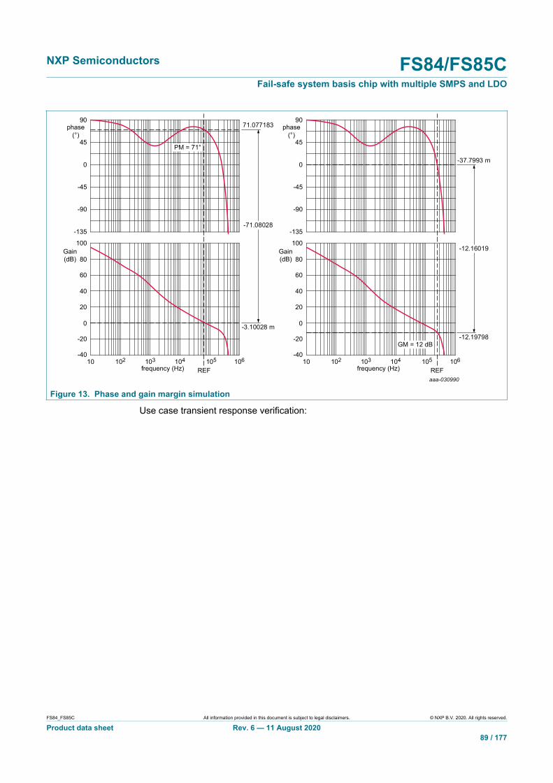
NXP Semiconductors FS84/FS85CFail-safe system basis chip with multiple SMPS and LDO
FS84_FS85C All information provided in this document is subject to legal disclaimers. © NXP B.V. 2020. All rights reserved.
Product data sheet Rev. 6 — 11 August 202089 / 177
aaa-030990
-71.08028
71.077183
-3.10028 m
REFfrequency (Hz)10 106105102 104103
-45
0
-90
45
90phase
(°)
-135
-40
60
40
20
0
-20
100
80Gain(dB)
PM = 71°
-12.16019
-37.7993 m
-12.19798
REFfrequency (Hz)10 106105102 104103
-45
0
-90
45
90phase
(°)
-135
-40
60
40
20
0
-20
100
80Gain(dB)
GM = 12 dB
Figure 13. Phase and gain margin simulation
Use case transient response verification:

NXP Semiconductors FS84/FS85CFail-safe system basis chip with multiple SMPS and LDO
FS84_FS85C All information provided in this document is subject to legal disclaimers. © NXP B.V. 2020. All rights reserved.
Product data sheet Rev. 6 — 11 August 202090 / 177
aaa-030991
4.1
4.0
4.2
4.3
VOUT(V)
3.9
time (ms) 200 µs / div0 1.00.80.4 0.60.2
1.0
2.0
3.0
4.0
I_OUT(A)
0
load step from 1 A to 3 A300 mA / µs
257.0194 µs 508.2793 µs251.2599 µs
REF A
min UV - 84 mV
max OV + 84 mV
167.3434 mV
4.1830110
4.0156676
Figure 14. Transient response simulation
20.4 Electrical characteristics
Table 80. Electrical characteristicsTA = −40 °C to 125 °C, unless otherwise specified. VSUP = VSUP_UVH to 36 V, unless otherwise specified. All voltagesreferenced to ground.
Symbol Parameter Min Typ Max Unit
VPRE
3.2 3.3 3.4 V
3.68 3.8 3.92 V
3.98 4.1 4.22 V
VPRE Output voltage (OTP_VPREV[5:0] bits)
4.85 5.0 5.15 V
Output voltage from 10 % to 90 % 250 450 650 μsVPRE_SOFT_START
Digital DAC soft start completion — — 1.35 ms
VPRE_STARTUP Overshoot at startup — — 3 %
VPRE_FB_OV Over voltage threshold protection 5.5 6.0 6.5 V
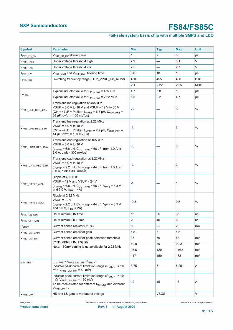
NXP Semiconductors FS84/FS85CFail-safe system basis chip with multiple SMPS and LDO
FS84_FS85C All information provided in this document is subject to legal disclaimers. © NXP B.V. 2020. All rights reserved.
Product data sheet Rev. 6 — 11 August 202091 / 177
Symbol Parameter Min Typ Max Unit
TPRE_FB_OV VPRE_FB_OV filtering time 1 2 3 μs
VPRE_UVH Under voltage threshold high 2.9 — 3.1 V
VPRE_UVL Under voltage threshold low 2.5 — 2.7 V
TPRE_UV VPRE_UVH and VPRE_UVL filtering time 6.0 10 15 μs
430 455 480 kHzFPRE_SW Switching frequency range (OTP_VPRE_clk_sel bit)
2.1 2.22 2.35 MHz
Typical inductor value for FPRE_SW = 455 kHz 4.7 6.8 10 μHLVPRE
Typical inductor value for FPRE_SW = 2.22 MHz 1.5 2.2 4.7 µH
VPRE_LINE_REG_455k
Transient line regulation at 455 kHzVSUP = 6.0 V to 18 V and VSUP = 12 V to 36 V(Cin = 47uF + PI filter, LVPRE = 6.8 µH, COUT_PRE =66 μF, dv/dt = 100 mV/μs)
-3 — 3 %
VPRE_LINE_REG_2.2M
Transient line regulation at 2.22 MHzVSUP = 6.0 V to 18 V(Cin = 47uF + PI filter, LVPRE = 2.2 µH, COUT_PRE =44 μF, dv/dt = 100 mV/μs)
-3 — 3 %
VPRE_LOAD_REG_455k
Transient load regulation at 455 kHzVSUP = 6.0 V to 36 V(LVPRE = 6.8 µH, COUT_PRE = 66 μF, from 1.0 A to3.0 A, di/dt = 300 mA/μs)
−3 — 3 %
VPRE_LOAD_REG_2.2M
Transient load regulation at 2.22MHzVSUP = 6.0 V to 18 V(LVPRE = 2.2 µH, COUT_PRE = 44 μF, from 1.0 A to3.0 A, di/dt = 300 mA/μs)
-3 — 3 %
VPRE_RIPPLE_455k
Ripple at 455 kHzVSUP = 12 V and VSUP = 24 V(LVPRE = 6.8 µH, COUT_PRE = 66 μF, VPRE = 3.3 Vand 5.0 V, IPRE = 4A)
-1 — 1 %
VPRE_RIPPLE_2.2M
Ripple at 2.22 MHzVSUP = 12 V(LVPRE = 2.2 µH, COUT_PRE = 44 μF, VPRE = 3.3 Vand 5.0 V, IPRE = 2A)
-0.5 — 0.5 %
TPRE_ON_MIN HS minimum ON time 15 25 35 ns
TPRE_OFF_MIN HS minimum OFF time 20 40 60 ns
RSHUNT Current sense resistor (±1 %) 10 — 20 mΩ
VPRE_LIM_GAIN Current sense amplifier gain 4.5 5 5.5
37 50 63 mV
60.8 80 99.2 mV
93.6 120 146.4 mV
VPRE_LIM_TH1 Current sense amplifier peak detection threshold(OTP_VPREILIM[1:0] bits)Note: 150mV setting is not available for 2.22 MHz
117 150 183 mV
ILIM_PRE = VPRE_LIM_TH / RSHUNTInductor peak current limitation range (RSHUNT = 10mΩ, VPRE_LIM_TH1 = 50 mV)
3.75 5 6.25 AILIM_PRE
Inductor peak current limitation range (RSHUNT = 10mΩ, VPRE_LIM_TH1 = 150 mV)To be recalculated for different RSHUNT and differentVPRE_LIM_TH
12 15 18 A
VPRE_DRV HS and LS gate driver output voltage — VBOS — V
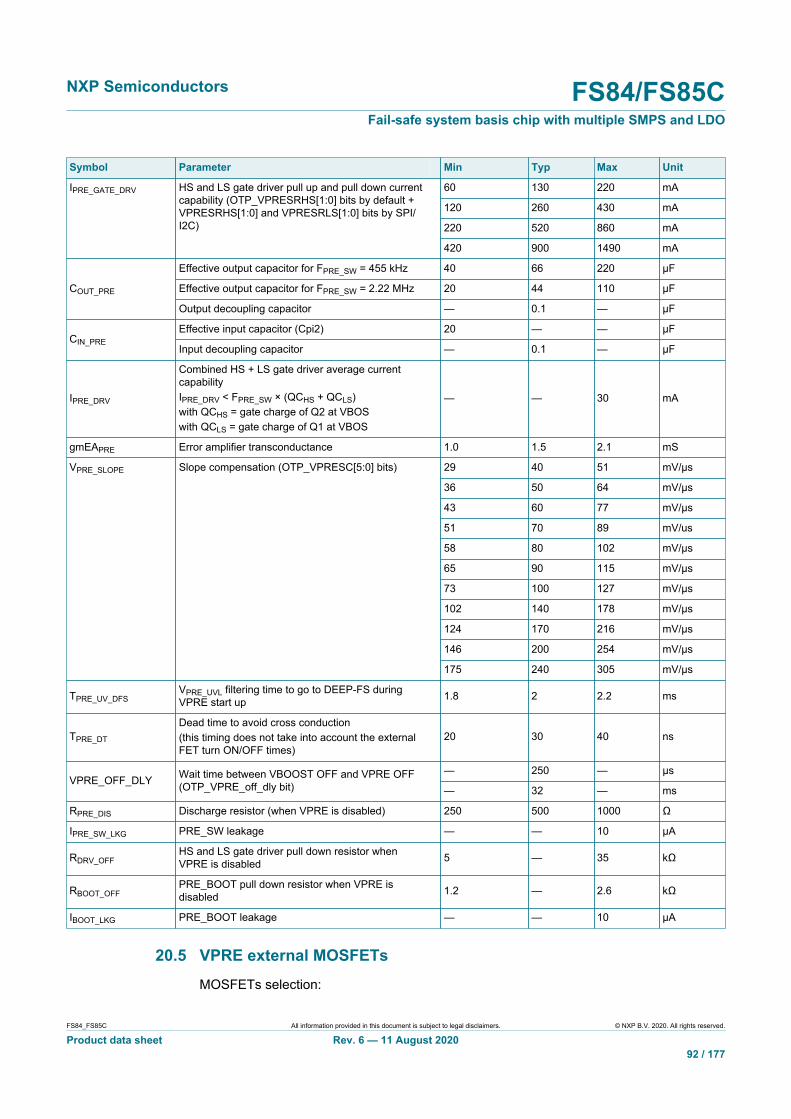
NXP Semiconductors FS84/FS85CFail-safe system basis chip with multiple SMPS and LDO
FS84_FS85C All information provided in this document is subject to legal disclaimers. © NXP B.V. 2020. All rights reserved.
Product data sheet Rev. 6 — 11 August 202092 / 177
Symbol Parameter Min Typ Max Unit
60 130 220 mA
120 260 430 mA
220 520 860 mA
IPRE_GATE_DRV HS and LS gate driver pull up and pull down currentcapability (OTP_VPRESRHS[1:0] bits by default +VPRESRHS[1:0] and VPRESRLS[1:0] bits by SPI/I2C)
420 900 1490 mA
Effective output capacitor for FPRE_SW = 455 kHz 40 66 220 μF
Effective output capacitor for FPRE_SW = 2.22 MHz 20 44 110 µFCOUT_PRE
Output decoupling capacitor — 0.1 — μF
Effective input capacitor (Cpi2) 20 — — μFCIN_PRE
Input decoupling capacitor — 0.1 — μF
IPRE_DRV
Combined HS + LS gate driver average currentcapabilityIPRE_DRV < FPRE_SW × (QCHS + QCLS)with QCHS = gate charge of Q2 at VBOSwith QCLS = gate charge of Q1 at VBOS
— — 30 mA
gmEAPRE Error amplifier transconductance 1.0 1.5 2.1 mS
29 40 51 mV/μs
36 50 64 mV/μs
43 60 77 mV/μs
51 70 89 mV/us
58 80 102 mV/μs
65 90 115 mV/μs
73 100 127 mV/μs
102 140 178 mV/μs
124 170 216 mV/μs
146 200 254 mV/μs
VPRE_SLOPE Slope compensation (OTP_VPRESC[5:0] bits)
175 240 305 mV/μs
TPRE_UV_DFSVPRE_UVL filtering time to go to DEEP-FS duringVPRE start up 1.8 2 2.2 ms
TPRE_DT
Dead time to avoid cross conduction(this timing does not take into account the externalFET turn ON/OFF times)
20 30 40 ns
— 250 — μsVPRE_OFF_DLY Wait time between VBOOST OFF and VPRE OFF
(OTP_VPRE_off_dly bit) — 32 — ms
RPRE_DIS Discharge resistor (when VPRE is disabled) 250 500 1000 Ω
IPRE_SW_LKG PRE_SW leakage — — 10 µA
RDRV_OFFHS and LS gate driver pull down resistor whenVPRE is disabled 5 — 35 kΩ
RBOOT_OFFPRE_BOOT pull down resistor when VPRE isdisabled 1.2 — 2.6 kΩ
IBOOT_LKG PRE_BOOT leakage — — 10 µA
20.5 VPRE external MOSFETsMOSFETs selection:

NXP Semiconductors FS84/FS85CFail-safe system basis chip with multiple SMPS and LDO
FS84_FS85C All information provided in this document is subject to legal disclaimers. © NXP B.V. 2020. All rights reserved.
Product data sheet Rev. 6 — 11 August 202093 / 177
• Logical level NMOS, gate drive comes from VBOS (5.0 V)• VDS > 60 V for 24 V truck, bus applications• VDS > 40 V for 12 V automotive applications• Qg < 15 nC at Vgs = 5.0 V is recommended for 455 kHz• Qg < 7 nC at Vgs = 5.0 V is recommended for 2.22MHz• Recommended references
Applications Fpre Ipre < 2.0 A Ipre < 4.0 A Ipre < 6.0 A Ipre < 10 A
455 kHz BUK9K25-40E,BUK9K18-40E
BUK9K25-40E,BUK9K18-40E BUK9K18-40E
BUK9K18-40E,NVTFS5C471NLWFTAG,HS = BUK9M9R5-40H,LS = BUK9M3R3-40H12 V
2.22 MHz BUK9K25-40E,BUK9Y29-40E
BUK9K25-40E,BUK9Y29-40E
BUK9K25-40E,BUK9Y29-40E N/A
24 V 455 kHz BUK9K35-60E,BUK9K52-60E
BUK9K35-60E,BUK9K52-60E BUK9K35-60E BUK9K12-60E
Other MOSFETs are possible but should have similar performances than therecommended references. The maximum current at 2.22 MHz is limited to 6 A for whichthe efficiency is equivalent to 10 A at 455 kHz. Above, the power dissipation in theexternal MOSFETs become important and the junction temperature may rise above 175°C.
VPRE switching slew rate can be configured by SPI/I2C to align with external MOSFETselection, VPRE switching frequency, and to optimize power dissipation and EMCperformance. It is recommended to configure the maximum slew rate by OTP and reduceit later by SPI/I2C if needed. FS85/FS84 is using current source to drive the externalMOSFET so adding an external serial resistor with the gate will not affect the slew rate.It is recommended to change the current source selection by SPI/I2C to change the slewrate.
VPRE MOSFET switching time can be estimated to TSW = (QGD + QGS / 2) /IPRE_GATE_DRV using the gate charge definition from Figure 15. QGD and QGS can beextracted from the MOSFET data sheet.
aaa-030992
VDS
ID
VGS(pl)
VGS
VGS(th)
QGS2
QGSQG(tot)
QGD
QGS1
Figure 15. MOSFET gate charge definition

NXP Semiconductors FS84/FS85CFail-safe system basis chip with multiple SMPS and LDO
FS84_FS85C All information provided in this document is subject to legal disclaimers. © NXP B.V. 2020. All rights reserved.
Product data sheet Rev. 6 — 11 August 202094 / 177
20.6 VPRE efficiencyVPRE efficiency versus current load is given for information based on externalcomponent criteria provided and VSUP voltage 14 V. If the conditions change, it has tobe recalculated with the FS85_PDTCAL tool. The real efficiency has to be verified bymeasurement at the application level.
Current (A)0
VPRE Efficiency
4 5321 6 8 97 10
aaa-035643
90
95
85
100Efficiency
(%)
75
80
5 V_455 kHz4.1 V_455 kHz3.3 V_455 kHz5 V_2.22 MHz4.1 V_2.22 MHz3.3 V_2.22 MHz
Cin
Ext. C and L
Ext. MOSFET's
47 µFFpre 455 kHz
ESR Cin 30 mΩCout
VPRE at 2.2 MHz: BUK9K25-40EVRPE at 455 kHz: BUK9K18-40E
60 µFESR Cout 10 mΩL coil 6.8 µHDCR coil 25
472220
3044102.225 mΩ
Rshunt 10 10 mΩ
GHS_drive 5 VHS_Rdson 17 mΩHS_QGtot 7 nCHS_QGD 3 nCHS_QGS 2 nCHS_Igate 900 mATHS_sw 5 nsGLS_drive 5 VLS_Rdson 17 mΩLS_QGtot 7 nCLS_QGD 3 nCLS_QGS 2 nC
LS_Igate 900 mATLS_sw 5
5245
2.41.4900
45
245
2.41.4
LS_QRR 16 nC7.6900
4 ns
Figure 16. VPRE theoretical efficiency
20.7 VPRE not populatedWhen two FS85/FS84 are used, only one VPRE may be required. It is possible to notpopulate the external components of the second VPRE to optimize the bill of material.
In that case, specific connection of the VPRE2 pins is required:
• PRE_FB2 must be connected to PRE_FB1• PRE_CSP2 must be connected to PRE_FB1• PRE_COMP2 must be left open• PRE_SW2 must be connected to GND• PRE_BOOT2 must be connected to VBOS2• PRE_GHS2 and PRE_GLS2 must be left open
After the startup phase, VPRE2 shall be disabled by SPI/I2C with VPDIS bit.
21 Low voltage boost: VBOOST

NXP Semiconductors FS84/FS85CFail-safe system basis chip with multiple SMPS and LDO
FS84_FS85C All information provided in this document is subject to legal disclaimers. © NXP B.V. 2020. All rights reserved.
Product data sheet Rev. 6 — 11 August 202095 / 177
21.1 Functional descriptionVBOOST block is a low voltage, asynchronous, peak current mode boost converter.VBOOST works in PWM and uses an external diode and an internal low-side FET.VBOOST enters Skip mode to maintain the correct output voltage in light load condition.The output voltage is configurable by OTP at 5.0 V or 5.74 V, the switching frequencyis 2.22 MHz and the output current is limited to 1.5 A peak input current. The input ofthe boost is connected to the output of VPRE. This block is intended to supply LDO1,LDO2, BUCK3 or an external regulator. The stability is ensured by an internal Type 2compensation network with slope compensation.
By default, VBOOST switching frequency is derived from the internal oscillator, and canbe synchronized with an external frequency signal applied on FIN input pin. The changefrom internal oscillator to external clock or vice versa is controlled by SPI/I2C.
An overcurrent detection and a thermal shutdown are implemented to protect the internalMOSFET. If an overcurrent is detected after the LS minimum TON time, the LS is turnedOFF and will be turned ON again at the next rising edge of the switching clock. Theovercurrent induces a duty cycle reduction that could lead to the output voltage graduallydropping, causing an undervoltage condition on one of the cascaded regulators.
Since the current limitation is on the input current, Table 81 summarizes the expectedoutput current capability depending on VPRE and VBOOST voltage configurations and L= 4.7 μH.
Table 81. Output current capabilityVPRE VBOOST IBOOST_OUT
5.0 V 800 mA3.3 V
5.74 V 700 mA
5.0 V 1 A4.1 V
5.74 V 900 mA
5.0 V 5.74 V 1.1 A
An overvoltage protection is implemented on BOOST_LS pin. When VBOOST_OV isdetected during two consecutive turn ON cycles, VBOOST is disabled. A SPI/I2Ccommand is required to enable it again. This monitoring is not safety related.

NXP Semiconductors FS84/FS85CFail-safe system basis chip with multiple SMPS and LDO
FS84_FS85C All information provided in this document is subject to legal disclaimers. © NXP B.V. 2020. All rights reserved.
Product data sheet Rev. 6 — 11 August 202096 / 177
21.2 Application schematic
aaa-030994
PWM
driver
EPAD
RCOMP
CCOMP
CHF
Vref
LBOOST
DBOOST
COUT_BOOST
BOOST_LS
VBOOST
BOOST
VBOOST
VPRE
CONTROLLER
SLOPECOMPENSATION
gm
Figure 17. BOOST schematic
It is recommended to select a Schottky diode for DBOOST to limit the impact on the SMPSefficiency.
21.3 Compensation network and stabilityThe internal compensation network, made with RCOMP, CCOMP and CHF is optimized forbest compromise between stability and transient response with RCOMP = 750 kΩ, CCOMP= 125 pF and CHF = 2.0 pF.
Use case with VBOOST = 5.74 V, LVBOOST = 4.7 μH, FBOOST_SW = 2.22 MHz, COUT_BOOST= 22 μF
Use case stability verification:
• Phase margin target PM > 45° and gain margin target GM > 6 dB.
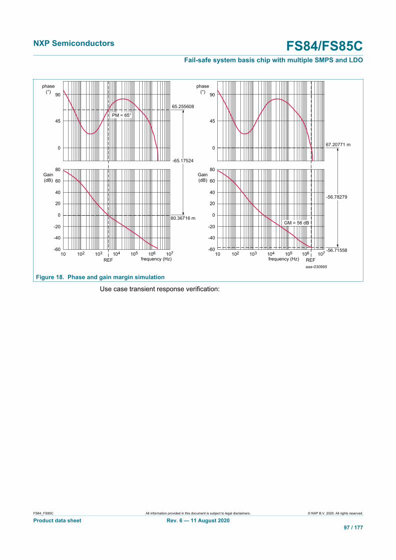
NXP Semiconductors FS84/FS85CFail-safe system basis chip with multiple SMPS and LDO
FS84_FS85C All information provided in this document is subject to legal disclaimers. © NXP B.V. 2020. All rights reserved.
Product data sheet Rev. 6 — 11 August 202097 / 177
aaa-030995
phase(°)
0
-20
20
-40
40
80
60Gain(dB)
-60
-65.17524
65.255608
80.36716 m
-56.78279
67.20771 m
-56.71558
frequency (Hz)10 107104 105 106102 103
REF REF
45
90
0
phase(°)
frequency (Hz)10 107104 105 106102 103
45
90
0
0
-20
20
-40
-60
40
80
60Gain(dB)
PM = 65°
GM = 56 dB
Figure 18. Phase and gain margin simulation
Use case transient response verification:
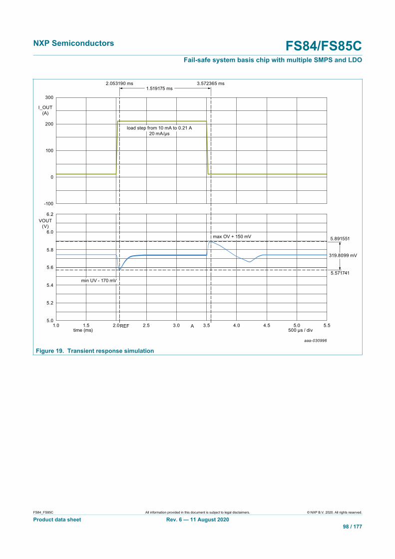
NXP Semiconductors FS84/FS85CFail-safe system basis chip with multiple SMPS and LDO
FS84_FS85C All information provided in this document is subject to legal disclaimers. © NXP B.V. 2020. All rights reserved.
Product data sheet Rev. 6 — 11 August 202098 / 177
aaa-030996
5.6
5.2
5.4
5.8
6.0
6.2VOUT
(V)
5.0
time (ms) 500 µs / div1.0 5.54.52.5 3.51.5 2.0 3.0 4.0 5.0
0
100
200
300
I_OUT(A)
-100
load step from 10 mA to 0.21 A20 mA/µs
2.053190 ms 3.572365 ms1.519175 ms
REF A
min UV - 170 mV
max OV + 150 mV
319.8099 mV
5.891551
5.571741
Figure 19. Transient response simulation
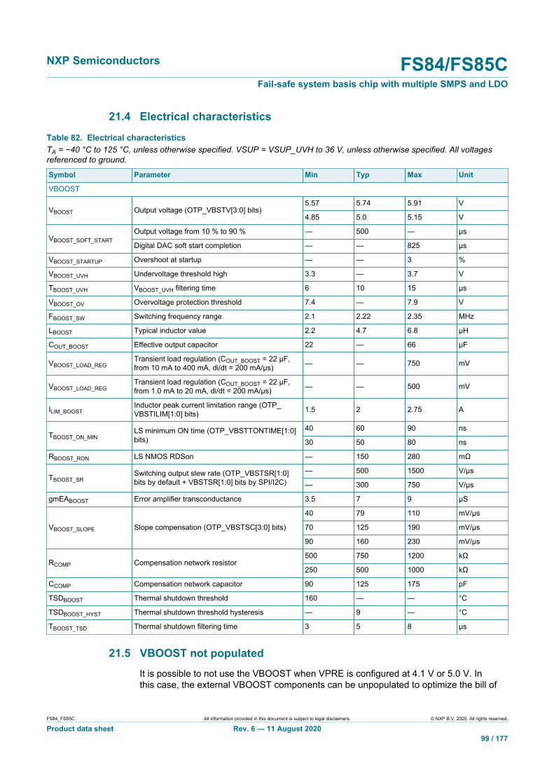
NXP Semiconductors FS84/FS85CFail-safe system basis chip with multiple SMPS and LDO
FS84_FS85C All information provided in this document is subject to legal disclaimers. © NXP B.V. 2020. All rights reserved.
Product data sheet Rev. 6 — 11 August 202099 / 177
21.4 Electrical characteristics
Table 82. Electrical characteristicsTA = −40 °C to 125 °C, unless otherwise specified. VSUP = VSUP_UVH to 36 V, unless otherwise specified. All voltagesreferenced to ground.
Symbol Parameter Min Typ Max Unit
VBOOST
5.57 5.74 5.91 VVBOOST Output voltage (OTP_VBSTV[3:0] bits)
4.85 5.0 5.15 V
Output voltage from 10 % to 90 % — 500 — μsVBOOST_SOFT_START
Digital DAC soft start completion — — 825 µs
VBOOST_STARTUP Overshoot at startup — — 3 %
VBOOST_UVH Undervoltage threshold high 3.3 — 3.7 V
TBOOST_UVH VBOOST_UVH filtering time 6 10 15 μs
VBOOST_OV Overvoltage protection threshold 7.4 — 7.9 V
FBOOST_SW Switching frequency range 2.1 2.22 2.35 MHz
LBOOST Typical inductor value 2.2 4.7 6.8 μH
COUT_BOOST Effective output capacitor 22 — 66 μF
VBOOST_LOAD_REGTransient load regulation (COUT_BOOST = 22 μF,from 10 mA to 400 mA, di/dt = 200 mA/μs) — — 750 mV
VBOOST_LOAD_REGTransient load regulation (COUT_BOOST = 22 μF,from 1.0 mA to 20 mA, di/dt = 200 mA/μs) — — 500 mV
ILIM_BOOSTInductor peak current limitation range (OTP_VBSTILIM[1:0] bits) 1.5 2 2.75 A
40 60 90 nsTBOOST_ON_MIN
LS minimum ON time (OTP_VBSTTONTIME[1:0]bits) 30 50 80 ns
RBOOST_RON LS NMOS RDSon — 150 280 mΩ
— 500 1500 V/μsTBOOST_SR
Switching output slew rate (OTP_VBSTSR[1:0]bits by default + VBSTSR[1:0] bits by SPI/I2C) — 300 750 V/μs
gmEABOOST Error amplifier transconductance 3.5 7 9 μS
40 79 110 mV/μs
70 125 190 mV/μsVBOOST_SLOPE Slope compensation (OTP_VBSTSC[3:0] bits)
90 160 230 mV/μs
500 750 1200 kΩRCOMP Compensation network resistor
250 500 1000 kΩ
CCOMP Compensation network capacitor 90 125 175 pF
TSDBOOST Thermal shutdown threshold 160 — — °C
TSDBOOST_HYST Thermal shutdown threshold hysteresis — 9 — °C
TBOOST_TSD Thermal shutdown filtering time 3 5 8 μs
21.5 VBOOST not populatedIt is possible to not use the VBOOST when VPRE is configured at 4.1 V or 5.0 V. Inthis case, the external VBOOST components can be unpopulated to optimize the bill of

NXP Semiconductors FS84/FS85CFail-safe system basis chip with multiple SMPS and LDO
FS84_FS85C All information provided in this document is subject to legal disclaimers. © NXP B.V. 2020. All rights reserved.
Product data sheet Rev. 6 — 11 August 2020100 / 177
material. The OTP_BOOSTEN bit shall be programmed to 0 and VBOOST pin must beconnected to VPRE. BOOST_LS pin must be left open.
VBOOST must be used when VPRE is configured at 3.3 V or 3.8 V to supply VBOS.
22 Low voltage buck: BUCK1 and BUCK2
22.1 Functional descriptionBUCK1 and BUCK2 blocks are low voltage, synchronous, valley current mode buckconverters with integrated HS PMOS and LS NMOS. BUCK1 and BUCK2 work in forcePWM and the output voltage is configurable by OTP from 0.8 V to 1.8 V, the switchingfrequency is 2.22 MHz and the output current is limited to 3.6 A peak . The input of theseblocks must be connected to the output of VPRE. The stability is ensured by an internalType 2 compensation network with slope compensation.
By default, BUCK1 and BUCK2 switching frequency is derived from the internal oscillatorand can be synchronized with an external frequency signal applied on FIN input pin. Thechange from internal oscillator to external clock or vice versa is controlled by SPI/I2C.
BUCK2 is part number dependent according to OTP_BUCK2EN bit. BUCK1 and BUCK2can work independently or in Dual phase mode to double the output current capability.When BUCK1 and BUCK2 are used in dual phase, they must have the same outputvoltage configuration. Any action like TSD, OV, disable by SPI/I2C, on BUCK1 affectsBUCK2 and vice versa.
An overcurrent detection and a thermal shutdown are implemented on BUCK1 andBUCK2 to protect the internal MOSFETs. The overcurrent induces a duty cycle reductionthat could lead to the output voltage gradually dropping, causing an undervoltagecondition.
The ramp up and ramp down of BUCK1 and BUCK2 when they are enabled and disabledis configurable with OTP_DVS_BUCK12[1:0] bits to accommodate multiple MCU softstart requirements. Static Voltage Scaling (SVS) feature is available to decrease theoutput voltage after power up during INIT_FS. Programmable phase shift control isimplemented, see Section 25 "Clock management".
22.2 Application schematic: Single phase modeIn this configuration, BUCK1 and BUCK2 are configured as independent outputs, workingindependently. Each output is configured and controlled independently by SPI/I2C.
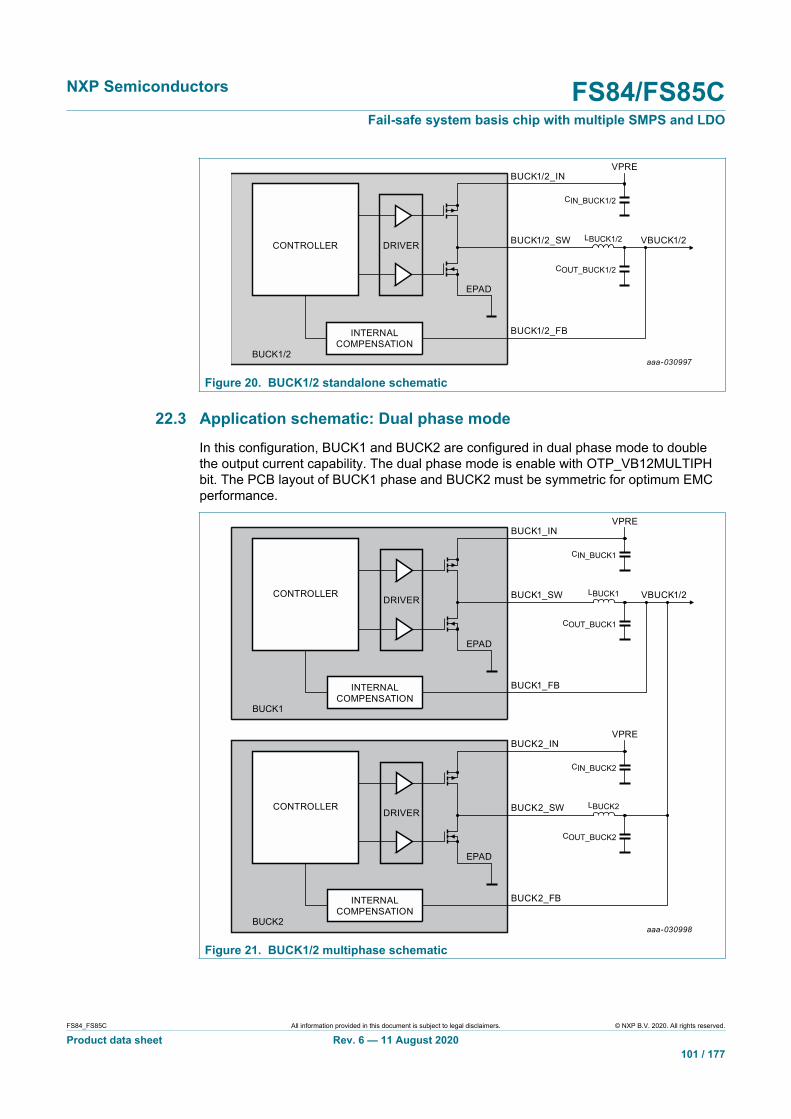
NXP Semiconductors FS84/FS85CFail-safe system basis chip with multiple SMPS and LDO
FS84_FS85C All information provided in this document is subject to legal disclaimers. © NXP B.V. 2020. All rights reserved.
Product data sheet Rev. 6 — 11 August 2020101 / 177
INTERNALCOMPENSATION
aaa-030997
DRIVER BUCK1/2_SW
BUCK1/2_FB
EPAD
BUCK1/2_IN
COUT_BUCK1/2
CIN_BUCK1/2
LBUCK1/2
VPRE
VBUCK1/2CONTROLLER
BUCK1/2
Figure 20. BUCK1/2 standalone schematic
22.3 Application schematic: Dual phase modeIn this configuration, BUCK1 and BUCK2 are configured in dual phase mode to doublethe output current capability. The dual phase mode is enable with OTP_VB12MULTIPHbit. The PCB layout of BUCK1 phase and BUCK2 must be symmetric for optimum EMCperformance.
INTERNALCOMPENSATION
DRIVER BUCK1_SW
BUCK1_FB
EPAD
BUCK1_IN
COUT_BUCK1
CIN_BUCK1
LBUCK1
VPRE
VBUCK1/2CONTROLLER
BUCK1
INTERNALCOMPENSATION
aaa-030998
DRIVER BUCK2_SW
BUCK2_FB
EPAD
BUCK2_IN
COUT_BUCK2
CIN_BUCK2
LBUCK2
VPRE
CONTROLLER
BUCK2
Figure 21. BUCK1/2 multiphase schematic
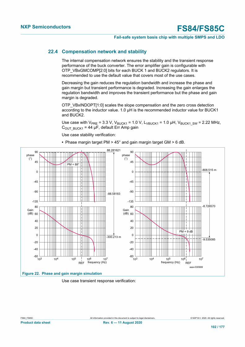
NXP Semiconductors FS84/FS85CFail-safe system basis chip with multiple SMPS and LDO
FS84_FS85C All information provided in this document is subject to legal disclaimers. © NXP B.V. 2020. All rights reserved.
Product data sheet Rev. 6 — 11 August 2020102 / 177
22.4 Compensation network and stabilityThe internal compensation network ensures the stability and the transient responseperformance of the buck converter. The error amplifier gain is configurable withOTP_VBxGMCOMP[2:0] bits for each BUCK 1 and BUCK2 regulators. It isrecommended to use the default value that covers most of the use cases.
Decreasing the gain reduces the regulation bandwidth and increase the phase andgain margin but transient performance is degraded. Increasing the gain enlarges theregulation bandwidth and improves the transient performance but the phase and gainmargin is degraded.
OTP_VBxINDOPT[1:0] scales the slope compensation and the zero cross detectionaccording to the inductor value. 1.0 μH is the recommended inductor value for BUCK1and BUCK2.
Use case with VPRE = 3.3 V, VBUCK1 = 1.0 V, LVBUCK1 = 1.0 μH, VBUCK1_SW = 2.22 MHz,COUT_BUCK1 = 44 μF, default Err Amp gain
Use case stability verification:
• Phase margin target PM > 45° and gain margin target GM > 6 dB.
aaa-030999
-45
0
-90
45
90phase
(°)
-135
frequency (Hz)103 107106104 105
REF
0
-20
20
-40
40
80
60Gain(dB)
-60
-88.58183
88.281621
-300.213 m
PM = 88°
-45
0
-90
45
90phase
(°)
-135
frequency (Hz)103 107106104 105
REF
0
-20
20
-40
40
80
60Gain(dB)
-60
-8.726570
-808.515 m
-9.535085
PM = 9 dB
Figure 22. Phase and gain margin simulation
Use case transient response verification:

NXP Semiconductors FS84/FS85CFail-safe system basis chip with multiple SMPS and LDO
FS84_FS85C All information provided in this document is subject to legal disclaimers. © NXP B.V. 2020. All rights reserved.
Product data sheet Rev. 6 — 11 August 2020103 / 177
aaa-031000
0.98
0.96
1.02
1.00
0.94
0.92
1.06
1.08
1.04
1.10VOUT
(V)
0.90
time (ms) 20 µs / div180 380340260 300220
1.0
1.4
0.6
1.8
2.2I(2-pos)
(A)
0.2
load step from 0.2 A to 2 A2 A / µs
REF A
min UV - 20 mV
max OV + 22 mV
1.0222327
42.92053 m
979.3122
Figure 23. Transient response simulation
22.5 Electrical characteristics
Table 83. Electrical characteristicsTA = −40 °C to 125 °C, unless otherwise specified. VSUP = VSUP_UVH to 36 V, unless otherwise specified. All voltagesreferenced to ground.
Symbol Parameter Min Typ Max Unit
BUCK1 and BUCK2
VBUCK12_IN Input voltage range 2.5 — 5.5 V
VBUCK12
Output voltage (OTP_VB1V[7:0] and OTP_VB2V[7:0] bits)0.8 V, 0.825 V, 0.9 V, 0.95 V, 0.975 V, 1.0 V,1.025 V, 1.03125 V, 1.075 V, 1.1 V, 1.1375 V, 1.2V, 1.25 V, 1.3 V, 1.35 V, 1.4 V, 1.5 V, 1.8 V
0.8 — 1.8 V
IBUCK12 DC output current capability (one phase) — 2.5 — A
VBUCK12_ACC Output voltage accuracy (IOUT < 2.5 A) −2 — +2 %
FBUCK12_SW Switching frequency range 2.1 2.22 2.35 MHz
LBUCK12Typical inductor value (OTP_VB1INDOPT[1:0]and OTP_VB2INDOPT[1:0] bits) 0.47 1.0 1.5 μH

NXP Semiconductors FS84/FS85CFail-safe system basis chip with multiple SMPS and LDO
FS84_FS85C All information provided in this document is subject to legal disclaimers. © NXP B.V. 2020. All rights reserved.
Product data sheet Rev. 6 — 11 August 2020104 / 177
Symbol Parameter Min Typ Max Unit
Effective output capacitor 40 — 160 μFCOUT_BUCK12
Output decoupling capacitor — 0.1 — μF
Effective input capacitor (close to BUCK1_IN andBUCK2_IN pins) 4.7 — — μF
CIN_BUCK12Input decoupling capacitor (close to BUCK1_INand BUCK2_IN pins) — 0.1 — μF
Transient load regulation for VBUCK12 < 1.2 V(Cout = 40 μF, from 200 mA to 1.0 A, di/dt = 2.0A/μs for mono phase configuration)(Cout = 40 μF, from 400 mA to 2.0 A, di/dt = 4.0A/μs for dual phase configuration)
−25 — +25 mV
VBUCK12_TLRTransient load regulation for VBUCK12 >1.2V(Cout = 40 μF, from 200 mA to 1.0 A, di/dt = 2.0A/μs for mono phase configuration)(Cout = 40 μF, from 400 mA to 2.0 A, di/dt = 4.0A/μs for dual phase configuration)
−3 — +3 %
2.0 2.6 3.1 A
ILIM_BUCK12
Inductor peak current limitation range for onephase(OTP_VB1SWILIM[1:0] bits and OTP_VB2SWILIM[1:0])
3.6 4.5 5.45 A
Ramp up speed, OTP_DVS_BUCK12[1:0] = 00 5.86 7.81 9.77 mV/μs
Ramp up speed, OTP_DVS_BUCK12[1:0] = 01 2.34 3.13 3.91 mV/µs
Ramp up speed, OTP_DVS_BUCK12[1:0] = 10 1.95 2.60 3.26 mV/µsVBUCK12_DVS_UP (forVBUCK12 up to 1.5V)
Ramp up speed, OTP_DVS_BUCK12[1:0] = 11 1.67 2.23 2.79 mV/µs
Ramp up speed, OTP_DVS_BUCK12[1:0] = 00 7.33 9.763 12.21 mV/μs
Ramp up speed, OTP_DVS_BUCK12[1:0] = 01 2.93 3.91 4.89 mV/µs
Ramp up speed, OTP_DVS_BUCK12[1:0] = 10 2.44 3.25 4.08 mV/µsVBUCK12_DVS_UP_1p8 (forVBUCK12 = 1.8V)
Ramp up speed, OTP_DVS_BUCK12[1:0] = 11 2.09 2.79 3.49 mV/µs
Ramp down speed, OTP_DVS_BUCK12[1:0] = 00 3.91 5.21 6.51 mV/µs
Ramp down speed, OTP_DVS_BUCK12[1:0] = 01 2.34 3.13 3.91 mV/µs
Ramp down speed, OTP_DVS_BUCK12[1:0] = 10 1.95 2.6 3.26 mV/µsVBUCK12_DVS_DOWN(forVBUCK12 up to 1.5V)
Ramp down speed, OTP_DVS_BUCK12[1:0] = 11 1.67 2.23 2.79 mV/µs
Ramp down speed, OTP_DVS_BUCK12[1:0] = 00 4.89 6.51 8.14 mV/µs
Ramp down speed, OTP_DVS_BUCK12[1:0] = 01 2.93 3.91 4.89 mV/µs
Ramp down speed, OTP_DVS_BUCK12[1:0] = 10 2.44 3.25 4.08 mV/µsVBUCK12_DVS_DOWN_1p8(for VBUCK12 = 1.8V)
Ramp down speed, OTP_DVS_BUCK12[1:0] = 11 2.09 2.79 3.49 mV/µs
VBUCK12_SOFT_START = VBUCK12 / VBUCK12_DVS_UPSoft start for VBUCK12 = 1.2 V andOTP_DVS_BUCK12[1:0] = 00
122.9 153.6 204.8 μs
TBUCK12_SOFT_START Soft start for VBUCK12 = 1.2 V andOTP_DVS_BUCK12[1:0] = 11To be recalculated for different VBUCK12 anddifferent VBUCK12_DVS_UP
430.1 538.1 718.5 µs
VBUCK12_STARTUP Overshoot at startup — — 50 mV
TBUCK12_OFF_MIN HS minimum OFF time 9 30 54 ns
TBUCK12_DT Dead time to avoid cross conduction 0.01 3 20 ns
RBUCK12_HS_RON HS PMOS RDSon — — 135 mΩ
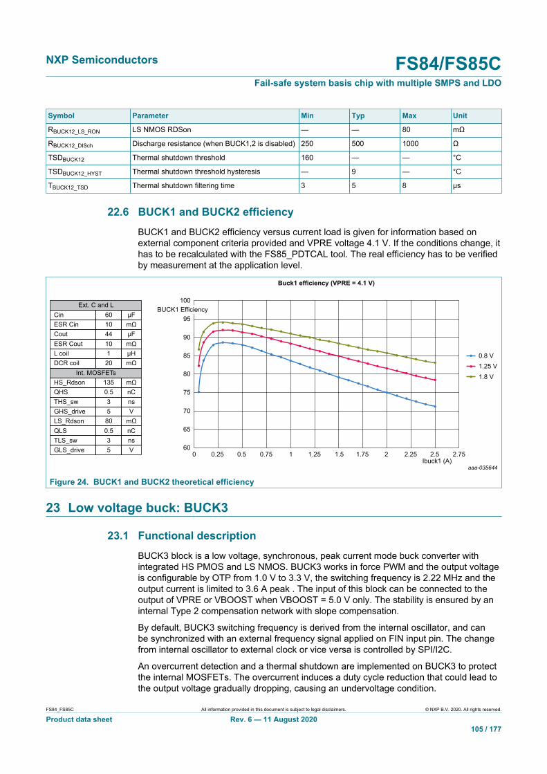
NXP Semiconductors FS84/FS85CFail-safe system basis chip with multiple SMPS and LDO
FS84_FS85C All information provided in this document is subject to legal disclaimers. © NXP B.V. 2020. All rights reserved.
Product data sheet Rev. 6 — 11 August 2020105 / 177
Symbol Parameter Min Typ Max Unit
RBUCK12_LS_RON LS NMOS RDSon — — 80 mΩ
RBUCK12_DISch Discharge resistance (when BUCK1,2 is disabled) 250 500 1000 Ω
TSDBUCK12 Thermal shutdown threshold 160 — — °C
TSDBUCK12_HYST Thermal shutdown threshold hysteresis — 9 — °C
TBUCK12_TSD Thermal shutdown filtering time 3 5 8 μs
22.6 BUCK1 and BUCK2 efficiencyBUCK1 and BUCK2 efficiency versus current load is given for information based onexternal component criteria provided and VPRE voltage 4.1 V. If the conditions change, ithas to be recalculated with the FS85_PDTCAL tool. The real efficiency has to be verifiedby measurement at the application level.
Ibuck1 (A)0 2.750.25 2.51.250.75 2.251.751 20.5 1.5
Buck1 efficiency (VPRE = 4.1 V)
aaa-035644
100
60
0.8 V1.25 V1.8 V
CinExt. C and L
Int. MOSFETs
60 µFESR Cin 10 mΩCout 44 µFESR Cout 10 mΩL coil 1 µHDCR coil 20 mΩ
HS_Rdson 135 mΩQHS 0.5 nCTHS_sw 3 nsGHS_drive 5 VLS_Rdson 80 mΩQLS 0.5 nCTLS_sw 3 nsGLS_drive 5 V
65
70
75
80
85
90
95BUCK1 Efficiency
Figure 24. BUCK1 and BUCK2 theoretical efficiency
23 Low voltage buck: BUCK3
23.1 Functional descriptionBUCK3 block is a low voltage, synchronous, peak current mode buck converter withintegrated HS PMOS and LS NMOS. BUCK3 works in force PWM and the output voltageis configurable by OTP from 1.0 V to 3.3 V, the switching frequency is 2.22 MHz and theoutput current is limited to 3.6 A peak . The input of this block can be connected to theoutput of VPRE or VBOOST when VBOOST = 5.0 V only. The stability is ensured by aninternal Type 2 compensation network with slope compensation.
By default, BUCK3 switching frequency is derived from the internal oscillator, and canbe synchronized with an external frequency signal applied on FIN input pin. The changefrom internal oscillator to external clock or vice versa is controlled by SPI/I2C.
An overcurrent detection and a thermal shutdown are implemented on BUCK3 to protectthe internal MOSFETs. The overcurrent induces a duty cycle reduction that could lead tothe output voltage gradually dropping, causing an undervoltage condition.

NXP Semiconductors FS84/FS85CFail-safe system basis chip with multiple SMPS and LDO
FS84_FS85C All information provided in this document is subject to legal disclaimers. © NXP B.V. 2020. All rights reserved.
Product data sheet Rev. 6 — 11 August 2020106 / 177
BUCK3 is part number dependent according to OTP_BUCK3EN bit. BUCK3_INQpin, used to bias internal BUCK3 driver, must be connected to the same source thanBUCK3_IN , either on VBOOST either on VPRE. See Application schematic. The rampup and ramp down of BUCK3 when it is enabled and disabled is configurable withOTP_DVS_BUCK3[1:0] bits to accommodate multiple MCU soft start requirements.
Programmable phase shift control is implemented, see Section 25 "Clock management".
23.2 Application schematic
INTERNALCOMPENSATION
aaa-031002
DRIVER BUCK3_SW
BUCK3_FB
EPAD
BUCK3_IN
BUCK3_INQ
COUT_BUCK3
CIN_BUCK3
LBUCK3
VPRE or VBOOST
VBUCK3CONTROLLER
BUCK3
Figure 25. BUCK3 schematic
23.3 Compensation network and stabilityThe internal compensation network ensures the stability and the transient responseperformance of the buck converter. OTP_VB3INDOPT[1:0] scales the slopecompensation and the zero cross detection according to inductor value. 1.0 μH is therecommended inductor value for BUCK3.
Use case with VPRE = 3.3 V, VBUCK3 = 2.3 V, LVBUCK3 = 1.0 μH, FBUCK3_SW = 2.22 MHz,COUT_BUCK3 = 44 μF
Use case stability verification:
• Phase margin target PM > 45° and gain margin target GM > 6 dB.

NXP Semiconductors FS84/FS85CFail-safe system basis chip with multiple SMPS and LDO
FS84_FS85C All information provided in this document is subject to legal disclaimers. © NXP B.V. 2020. All rights reserved.
Product data sheet Rev. 6 — 11 August 2020107 / 177
aaa-031003
0
45
-45
90
135phase
(°)
-90
frequency (Hz)103 107106104 105
REF
-20
-40
0
-60
20
60
40Gain(dB)
-80
-65.72816
65.577201
-150.958 m
PM = 65°
0
45
-45
90
135phase
(°)
-90
frequency (Hz)103 107106104 105
REF
-20
-40
0
-60
20
60
40Gain(dB)
-80
-26.56473
-541.098 m
-27.10583
PM = 26 dB
Figure 26. Phase and gain margin simulation
Use case transient response verification:
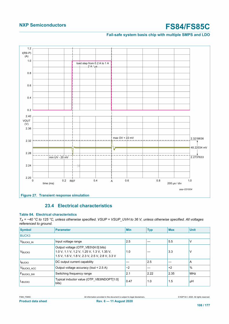
NXP Semiconductors FS84/FS85CFail-safe system basis chip with multiple SMPS and LDO
FS84_FS85C All information provided in this document is subject to legal disclaimers. © NXP B.V. 2020. All rights reserved.
Product data sheet Rev. 6 — 11 August 2020108 / 177
aaa-031004
2.40
2.28
2.32
2.24
2.36
2.40VOUT
(V)
2.20
time (ms) 200 µs / div0 1.00.80.4 0.60.2
0.6
0.8
0.4
1.0
1.2I(R9-P)
(A)
0.2
load step from 0.2 A to 1 A2 A / µs
REF A
min UV - 20 mV
max OV + 22 mV
48.22034 mV
2.3219836
2.2737633
Figure 27. Transient response simulation
23.4 Electrical characteristics
Table 84. Electrical characteristicsTA = −40 °C to 125 °C, unless otherwise specified. VSUP = VSUP_UVH to 36 V, unless otherwise specified. All voltagesreferenced to ground.
Symbol Parameter Min Typ Max Unit
BUCK3
VBUCK3_IN Input voltage range 2.5 — 5.5 V
VBUCK3
Output voltage (OTP_VB3V[4:0] bits)1.0 V, 1.1 V, 1.2 V, 1.25 V, 1.3 V, 1.35 V,1.5 V, 1.6 V, 1.8 V, 2.3 V, 2.5 V, 2.8 V, 3.3 V
1.0 — 3.3 V
IBUCK3 DC output current capability — 2.5 — A
VBUCK3_ACC Output voltage accuracy (Iout < 2.5 A) −2 — +2 %
FBUCK3_SW Switching frequency range 2.1 2.22 2.35 MHz
LBUCK3Typical inductor value (OTP_VB3INDOPT[1:0]bits) 0.47 1.0 1.5 μH

NXP Semiconductors FS84/FS85CFail-safe system basis chip with multiple SMPS and LDO
FS84_FS85C All information provided in this document is subject to legal disclaimers. © NXP B.V. 2020. All rights reserved.
Product data sheet Rev. 6 — 11 August 2020109 / 177
Symbol Parameter Min Typ Max Unit
Effective output capacitor 40 — 120 μFCOUT_BUCK3
Output decoupling capacitor — 0.1 — μF
Effective input capacitor (close to BUCK3_IN pin) 4.7 — — μFCIN_BUCK3 Input decoupling capacitor (close to BUCK3_IN
pin) — 0.1 — μF
VBUCK3_TLRTransient load regulation (Cout = 40 μF, from 200mA to 1.0 A, di/dt = 2.0 A/μs) −50 — +50 mV
2.0 2.6 3.1 AILIM_BUCK3
Inductor peak current limitation range (OTP_VB3SWILIM[1:0] bits) 3.6 4.5 5.45 A
TBUCK3_ON_MIN HS minimum ON time 5 50 80 ns
Ramp up and ramp down speed, OTP_DVS_BUCK3[1:0] = 00 7.81 10.42 13.02 mV/µs
Ramp up and ramp down speed, OTP_DVS_BUCK3[1:0] = 01 2.6 3.47 4.34 mV/µs
Ramp up and ramp down speed, OTP_DVS_BUCK3[1:0] = 10 1.95 2.6 3.26 mV/µs
VBUCK3_DVS_UP_DOWN
Ramp up and ramp down speed, OTP_DVS_BUCK3[1:0] = 11 1.56 2.08 2.60 mV/µs
VBUCK3_SOFT_START = VBUCK3 /VBUCK3_DVS_UP_DOWNSoft start for VBUCK3 = 1.1 V andOTP_DVS_BUCK3[1:0] = 00
84.8 105.6 140.8 µs
TBUCK3_SOFT_STARTSoft start for VBUCK3 = 1.1 V andOTP_DVS_BUCK3[1:0] = 11To be recalculated for different VBUCK3 anddifferent VBUCK3_DVS_UP_DOWN
422.4 528 704 µs
VBUCK3_STARTUP Overshoot at startup — — 50 mV
TBUCK3_DT Dead time to avoid cross conduction 0.01 3 20 ns
RBUCK3_HS_RON HS PMOS RDSon — — 135 mΩ
RBUCK3_LS_RON LS NMOS RDSon — — 80 mΩ
RBUCK3_DISCH Discharge resistance (when BUCK3 is disabled) 250 500 1000 Ω
TSDBUCK3 Thermal shutdown threshold 160 — — °C
TSDBUCK3_HYST Thermal shutdown threshold hysteresis — 9 — °C
TBUCK3_TSD Thermal shutdown filtering time 3 5 8 μs
23.5 BUCK3 efficiencyBUCK3 efficiency versus current load is given for information based on externalcomponent criteria provided and VPRE voltage 4.1 V. If the conditions change, it hasto be recalculated with the FS85_PDTCAL tool. The real efficiency has to be verified bymeasurement at the application level.
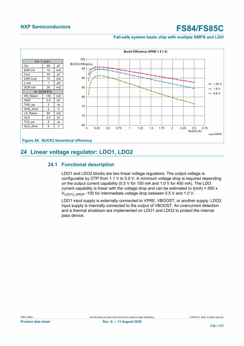
NXP Semiconductors FS84/FS85CFail-safe system basis chip with multiple SMPS and LDO
FS84_FS85C All information provided in this document is subject to legal disclaimers. © NXP B.V. 2020. All rights reserved.
Product data sheet Rev. 6 — 11 August 2020110 / 177
Ibuck3 (A)0 2.750.25 2.51.250.75 2.251.751 20.5 1.5
Buck3 Efficiency (VPRE = 4.1 V)
aaa-035645
100
65
1.25 V1.8 V0.8 V
CinExt. C and L
Int. MOSFETs
60 µFESR Cin 10 mΩCout 44 µFESR Cout 10 mΩL coil 1 µHDCR coil 20 mΩ
HS_Rdson 135 mΩQHS 0.5 nCTHS_sw 3 nsGHS_drive 5 VLS_Rdson 80 mΩQLS 0.5 nCTLS_sw 3 nsGLS_drive 5 V
BUCK3 Efficiency
70
75
80
85
90
95
Figure 28. BUCK3 theoretical efficiency
24 Linear voltage regulator: LDO1, LDO2
24.1 Functional descriptionLDO1 and LDO2 blocks are two linear voltage regulators. The output voltage isconfigurable by OTP from 1.1 V to 5.0 V. A minimum voltage drop is required dependingon the output current capability (0.5 V for 150 mA and 1.0 V for 400 mA). The LDOcurrent capability is linear with the voltage drop and can be estimated to I(mA) = 500 xVLDO12_DROP -100 for intermediate voltage drop between 0.5 V and 1.0 V.
LDO1 input supply is externally connected to VPRE, VBOOST, or another supply. LDO2input supply is internally connected to the output of VBOOST. An overcurrent detectionand a thermal shutdown are implemented on LDO1 and LDO2 to protect the internalpass device.
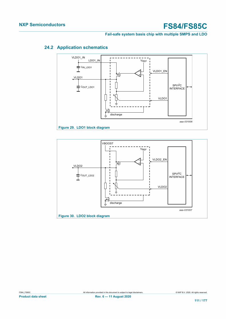
NXP Semiconductors FS84/FS85CFail-safe system basis chip with multiple SMPS and LDO
FS84_FS85C All information provided in this document is subject to legal disclaimers. © NXP B.V. 2020. All rights reserved.
Product data sheet Rev. 6 — 11 August 2020111 / 177
24.2 Application schematics
aaa-031006
SPI/I2CINTERFACE
VLDO1_EN
LDO1_IN
VLDO1
CIN_LDO1
COUT_LDO1
VLDO1_IN
discharge
VREF
VLDO1
Figure 29. LDO1 block diagram
aaa-031007
SPI/I2CINTERFACE
VLDO2_EN
VLDO2
VBOOST
COUT_LDO2
discharge
VREF
VLDO2
Figure 30. LDO2 block diagram
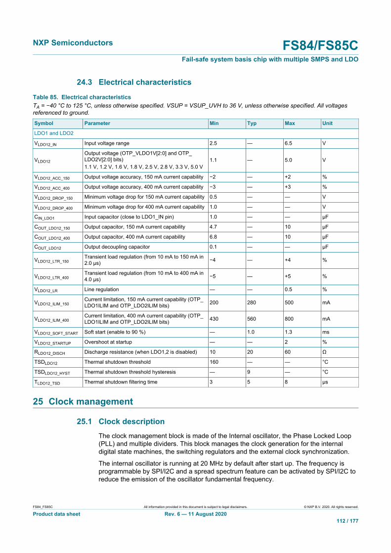
NXP Semiconductors FS84/FS85CFail-safe system basis chip with multiple SMPS and LDO
FS84_FS85C All information provided in this document is subject to legal disclaimers. © NXP B.V. 2020. All rights reserved.
Product data sheet Rev. 6 — 11 August 2020112 / 177
24.3 Electrical characteristics
Table 85. Electrical characteristicsTA = −40 °C to 125 °C, unless otherwise specified. VSUP = VSUP_UVH to 36 V, unless otherwise specified. All voltagesreferenced to ground.
Symbol Parameter Min Typ Max Unit
LDO1 and LDO2
VLDO12_IN Input voltage range 2.5 — 6.5 V
VLDO12
Output voltage (OTP_VLDO1V[2:0] and OTP_LDO2V[2:0] bits)1.1 V, 1.2 V, 1.6 V, 1.8 V, 2.5 V, 2.8 V, 3.3 V, 5.0 V
1.1 — 5.0 V
VLDO12_ACC_150 Output voltage accuracy, 150 mA current capability −2 — +2 %
VLDO12_ACC_400 Output voltage accuracy, 400 mA current capability −3 — +3 %
VLDO12_DROP_150 Minimum voltage drop for 150 mA current capability 0.5 — — V
VLDO12_DROP_400 Minimum voltage drop for 400 mA current capability 1.0 — — V
CIN_LDO1 Input capacitor (close to LDO1_IN pin) 1.0 — — μF
COUT_LDO12_150 Output capacitor, 150 mA current capability 4.7 — 10 μF
COUT_LDO12_400 Output capacitor, 400 mA current capability 6.8 — 10 μF
COUT_LDO12 Output decoupling capacitor 0.1 — — μF
VLDO12_LTR_150Transient load regulation (from 10 mA to 150 mA in2.0 μs) −4 — +4 %
VLDO12_LTR_400Transient load regulation (from 10 mA to 400 mA in4.0 μs) −5 — +5 %
VLDO12_LR Line regulation — — 0.5 %
VLDO12_ILIM_150Current limitation, 150 mA current capability (OTP_LDO1ILIM and OTP_LDO2ILIM bits) 200 280 500 mA
VLDO12_ILIM_400Current limitation, 400 mA current capability (OTP_LDO1ILIM and OTP_LDO2ILIM bits) 430 560 800 mA
VLDO12_SOFT_START Soft start (enable to 90 %) — 1.0 1.3 ms
VLDO12_STARTUP Overshoot at startup — — 2 %
RLDO12_DISCH Discharge resistance (when LDO1,2 is disabled) 10 20 60 Ω
TSDLDO12 Thermal shutdown threshold 160 — — °C
TSDLDO12_HYST Thermal shutdown threshold hysteresis — 9 — °C
TLDO12_TSD Thermal shutdown filtering time 3 5 8 μs
25 Clock management
25.1 Clock descriptionThe clock management block is made of the Internal oscillator, the Phase Locked Loop(PLL) and multiple dividers. This block manages the clock generation for the internaldigital state machines, the switching regulators and the external clock synchronization.
The internal oscillator is running at 20 MHz by default after start up. The frequency isprogrammable by SPI/I2C and a spread spectrum feature can be activated by SPI/I2C toreduce the emission of the oscillator fundamental frequency.

NXP Semiconductors FS84/FS85CFail-safe system basis chip with multiple SMPS and LDO
FS84_FS85C All information provided in this document is subject to legal disclaimers. © NXP B.V. 2020. All rights reserved.
Product data sheet Rev. 6 — 11 August 2020113 / 177
VPRE switching frequency is coming from CLK2 (455 kHz) or CLK1 (2.22 MHz).BUCK1,2,3 and BOOST switching frequency is coming from CLK1 (2.22 MHz). Theswitching regulators can be synchronized with an external frequency coming from FINpin. A dedicated watchdog monitoring is implemented to verify and report the correct FINfrequency range. Different clocks can be sent to FOUT pin to synchronize an external ICor for diagnostic.
aaa-031008
20 MHz INT. OSC(SPREAD SPECTRUM,
FREQ TUNING)enable
CLK2
CLK1
PLL x 48
out
in
DIVIDER/48
DIVIDER 2/44 (OTP)
PHASESHIFTING
FOUT_clkVPRE_clk
BUCK1,2,3_clkBOOST_clk
FOUT
PHASESHIFTING0
1FIN
VDDI2C
DIVIDER/1, /6
CLK_FIN_DIVMONITORING
OSC_MAIN/48
CLK_FIN_DIV
EXT_FIN_SELEXT_FIN_DIS
Vddio
FOUT_MUX_SEL
FOUT_clkVPRE_clk
BUCKs & BOOST_clkCLK_FIN_DIVOSC_Main/48
OSC_FS/48
DIVIDER 1/9 (OTP)
0
1OTP:PLL_SEL
Figure 31. Clock management block diagram
25.2 Phase shiftingThe clocks of the switching regulators (VPRE_clk, BOOST_clk, BUCK1_clk, BUCK2_clkand BUCK3_clk) can be delayed in order to avoid all the regulators to turn ON at thesame time to reduce peak current and improve EMC performance.
Each clock of each regulator can be shifted from 1 to 7 clock cycles of CLK runningat 20 MHz what corresponds to 50 ns. The phase shift configuration is done by OTPconfiguration using OTP_VPRE_ph[2:0], OTP_VBST_ph[2:0], OTP_BUCK1_ph[2:0],OTP_BUCK2_ph[2:0] and OTP_BUCK3_ph[2:0].
VPRE and BUCK3 have a peak current detection architecture. The PWM synchronizesthe turn ON of the high-side switch. BUCK1 and BUCK2 have a valley current detectionarchitecture. The PWM synchronizes the turn ON of the low-side switch.
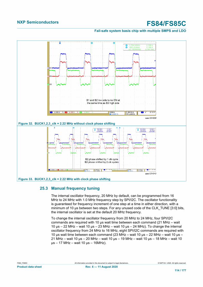
NXP Semiconductors FS84/FS85CFail-safe system basis chip with multiple SMPS and LDO
FS84_FS85C All information provided in this document is subject to legal disclaimers. © NXP B.V. 2020. All rights reserved.
Product data sheet Rev. 6 — 11 August 2020114 / 177
Figure 32. BUCK1,2,3_clk = 2.22 MHz without clock phase shifting
Figure 33. BUCK1,2,3_clk = 2.22 MHz with clock phase shifting
25.3 Manual frequency tuningThe internal oscillator frequency, 20 MHz by default, can be programmed from 16MHz to 24 MHz with 1.0 MHz frequency step by SPI/I2C. The oscillator functionalityis guaranteed for frequency increment of one step at a time in either direction, with aminimum of 10 μs between two steps. For any unused code of the CLK_TUNE [3:0] bits,the internal oscillator is set at the default 20 MHz frequency.
To change the internal oscillator frequency from 20 MHz to 24 MHz, four SPI/I2Ccommands are required with 10 μs wait time between each command (21 MHz – wait10 μs – 22 MHz – wait 10 μs – 23 MHz – wait 10 μs – 24 MHz). To change the internaloscillator frequency from 24 MHz to 16 MHz, eight SPI/I2C commands are required with10 μs wait time between each command (23 MHz – wait 10 μs – 22 MHz – wait 10 μs –21 MHz – wait 10 μs – 20 MHz – wait 10 μs – 19 MHz – wait 10 μs – 18 MHz – wait 10μs – 17 MHz – wait 10 μs – 16MHz).

NXP Semiconductors FS84/FS85CFail-safe system basis chip with multiple SMPS and LDO
FS84_FS85C All information provided in this document is subject to legal disclaimers. © NXP B.V. 2020. All rights reserved.
Product data sheet Rev. 6 — 11 August 2020115 / 177
Table 86. Manual frequency tuning configurationCLK_TUNE [3:0] Oscillator frequency [MHz]
0000 (default) 20
0001 21
0010 22
0011 23
0100 24
1001 16
1010 17
1011 18
1100 19
Reset condition POR
25.4 Spread spectrumThe internal oscillator can be modulated with a triangular carrier frequency of 23 kHz or94 kHz with ±5 % deviation range around the oscillator frequency. The spread spectrumfeature can be activated by SPI/I2C with the MOD_EN bit and the carrier frequency canbe selected by SPI/I2C with the MOD_CONF bit. By default, the spread spectrum isdisabled. The spread spectrum and the manual frequency tuning functions cannot beused at the same time.
The main purpose of the spread spectrum is to improve the EMC performance byspreading the energy of the internal oscillator and VPRE frequency on VBAT frequencyspectrum. It is recommended to select 23 kHz carrier frequency when VPRE isconfigured at 455 kHz and 94 kHz when VPRE is configured at 2.2 MHz for the bestperformance.
25.5 External clock synchronizationTo synchronize the switching regulators with an external frequency coming from FINpin, the PLL shall be enabled with OTP_PLL_SEL bit. The FIN pin accepts two rangesof frequency depending on the divider selection to always have CLK clock at the outputof the PLL in the working range of the digital blocks from 16 MHz to 24 MHz. WhenFIN_DIV = 0, the input frequency range must be between 333 kHz and 500 kHz. WhenFIN_DIV = 1, the input frequency range must be between 2.0 MHz and 3.0 MHz.
After the FIN clock divider configuration with FIN_DIV bit, the FIN clock is routed to thePLL input with EXT_FIN_SEL bit. The CLK clock changes from the internal oscillator toFIN external clock with EXT_FIN_SEL bit. So, the configuration procedure is FIN_DIVfirst, then apply FIN and finally set EXT_FIN_SEL.
If FIN is out of range, CLK clock moves back to the internal oscillator and reportsthe error using the CLK_FIN_DIV_OK bit. When FIN comes back in the range, theconfiguration procedure described above shall be executed again.
The FOUT pin can be used to synchronize an external device with the FS85/FS84. Thefrequency sent to FOUT is selected by SPI/I2C with the FOUT_MUX_SEL [3:0] bits.
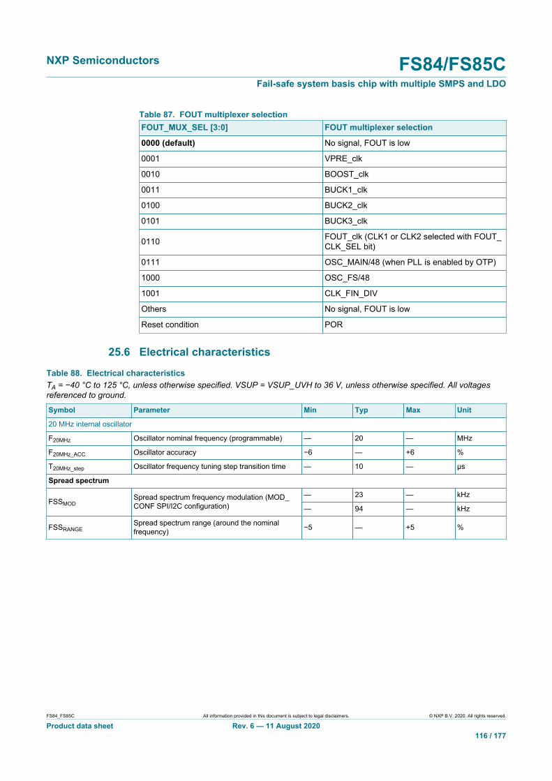
NXP Semiconductors FS84/FS85CFail-safe system basis chip with multiple SMPS and LDO
FS84_FS85C All information provided in this document is subject to legal disclaimers. © NXP B.V. 2020. All rights reserved.
Product data sheet Rev. 6 — 11 August 2020116 / 177
Table 87. FOUT multiplexer selectionFOUT_MUX_SEL [3:0] FOUT multiplexer selection
0000 (default) No signal, FOUT is low
0001 VPRE_clk
0010 BOOST_clk
0011 BUCK1_clk
0100 BUCK2_clk
0101 BUCK3_clk
0110 FOUT_clk (CLK1 or CLK2 selected with FOUT_CLK_SEL bit)
0111 OSC_MAIN/48 (when PLL is enabled by OTP)
1000 OSC_FS/48
1001 CLK_FIN_DIV
Others No signal, FOUT is low
Reset condition POR
25.6 Electrical characteristics
Table 88. Electrical characteristicsTA = −40 °C to 125 °C, unless otherwise specified. VSUP = VSUP_UVH to 36 V, unless otherwise specified. All voltagesreferenced to ground.
Symbol Parameter Min Typ Max Unit
20 MHz internal oscillator
F20MHz Oscillator nominal frequency (programmable) — 20 — MHz
F20MHz_ACC Oscillator accuracy −6 — +6 %
T20MHz_step Oscillator frequency tuning step transition time — 10 — μs
Spread spectrum
— 23 — kHzFSSMOD
Spread spectrum frequency modulation (MOD_CONF SPI/I2C configuration) — 94 — kHz
FSSRANGESpread spectrum range (around the nominalfrequency) −5 — +5 %
NXP Semiconductors FS84/FS85CFail-safe system basis chip with multiple SMPS and LDO
FS84_FS85C All information provided in this document is subject to legal disclaimers. © NXP B.V. 2020. All rights reserved.
Product data sheet Rev. 6 — 11 August 2020117 / 177
Symbol Parameter Min Typ Max Unit
Clock synchronization (FIN)
VFIN_IN Input voltage range — VDDI2C — V
DCFIN_FOUT FIN and FOUT duty cycle 40 50 60 %
333 417 500 kHzFINRANGE
FIN input frequency range (FIN_DIV SPI/I2Cconfiguration) 2.25 2.5 2.75 MHz
FINVIL FIN low voltage threshold 0.3 x VDDI2C — — V
FINVIH FIN high voltage threshold — — 0.7 x VDDI2C V
FINHYST FIN hysteresis 0.1 — — V
FINIPD FIN internal pull down current source 7 10 13 μA
FINDLY FIN input buffer propagation delay — — 8 ns
FINERR_LONGCLK_FIN_DIV monitoring, long deviationdetection 5 — — μs
FINERR_SHORTCLK_FIN_DIV monitoring, short deviationdetection — — 1.5 μs
FINTLOSTTime to switch to internal oscillator when FIN islost — — 3 μs
Clock synchronization (FOUT)
VFOUT_OUT Output voltage range — VDDIO — V
FOUTVOL FOUT low voltage threshold at 2.0 mA — — 0.5 V
FOUTVOH FOUT high voltage threshold at −2.0 mA VDDIO − 0.5 — — V
IFOUT Tri-state leakage current (VDDIO = 5.0 V) −1.0 — 1.0 μA
FOUTTRISEFOUT rise time (from 20 % to 80 % of VDDIO,Cout = 30 pF) — — 20 ns
FOUTTFALLFOUT fall time (from 80 % to 20 % of VDDIO,Cout = 30 pF) — — 20 ns
PLLTLOCK PLL lock time — — 90 μs
PLLTSETPLL settling time (from EXT_FIN_DIS enable to±1 % of output frequency) — — 125 μs

NXP Semiconductors FS84/FS85CFail-safe system basis chip with multiple SMPS and LDO
FS84_FS85C All information provided in this document is subject to legal disclaimers. © NXP B.V. 2020. All rights reserved.
Product data sheet Rev. 6 — 11 August 2020118 / 177
26 Analog multiplexer: AMUX
26.1 Functional descriptionThe AMUX pin delivers 32 analog voltage channels to the MCU ADC input. The voltagechannels delivered to AMUX pin can be selected by SPI/I2C. The maximum AMUXoutput voltage range is VDDIO. External Rs/Cout components are required for the bufferstability.
26.2 Block diagram
aaa-031011
channels_x
signalssignals /2.5signals
/7.5 or /14
SPI/I2C x
z
channels_yy
channels_z
AGND
VDDIO
AMUX to MCU ADC
Cout = 10 nF
Rs = 220 Ωbuffer
AMUX [4:0]
R1
R2R4
R3
R5
Figure 34. AMUX block diagram
26.3 AMUX channel selection
Table 89. AMUX output selectionAMUX[4:0] Signal selection for AMUX output
00000 (default) GND
00001 VDDIO voltage
00010 Temperature sensor : T(°C) = [(VAMUX – VTEMP25) /VTEMP_COEFF] + 25
00011 Bandgap main: 1.0 V ±1 %
00100 Bandgap fail-safe: 1.0 V ±1 %
00101 VBUCK1 voltage
00110 VBUCK2 voltage
00111 VBUCK3 voltage divided by 2.5
01000 VPRE voltage divided by 2.5
01001 VBOOST voltage divided by 2.5
01010 VLDO1 voltage divided by 2.5
01011 VLDO2 voltage divided by 2.5
01100 VBOS voltage divided by 2.5
01101 Reserved
01110 VSUP1 voltage divided by 7.5 or 14 (SPI/I2C configurationwith bit RATIO)
NXP Semiconductors FS84/FS85CFail-safe system basis chip with multiple SMPS and LDO
FS84_FS85C All information provided in this document is subject to legal disclaimers. © NXP B.V. 2020. All rights reserved.
Product data sheet Rev. 6 — 11 August 2020119 / 177
AMUX[4:0] Signal selection for AMUX output
01111 WAKE1 voltage divided by 7.45 or 13.85 (SPI/I2Cconfiguration with bit RATIO)
10000 WAKE2 voltage divided by 7.45 or 13.85 (SPI/I2Cconfiguration with bit RATIO)
10001 Vana: internal main analog voltage supply: 1.6 V ±2 %
10010 Vdig: internal main digital voltage supply: 1.6 V ±2 %
10011 Vdig_fs: internal fail-safe digital voltage supply: 1.6 V ±2 %
10100 PSYNC voltage
Others Same as default value (00000): GND
26.4 Electrical characteristics
Table 90. Electrical characteristicsTA = −40 °C to 125 °C, unless otherwise specified. VSUP = VSUP_UVH to 36 V, unless otherwise specified. All voltagesreferenced to ground.
Symbol Parameter Min Typ Max Unit
AMUX
VAMUX_VDDIO Minimum VDDIO operating voltage for AMUX 3.2 — — V
VAMUX_IN
Input voltage range for VSUP, WAKE1, WAKE2• Ratio 7.45 and 7.5• Ratio 13.85 and 14
2.254.2
——
22.542
V
IAMUX Output buffer current capability — — 2.0 mA
VAMUX_OFF Offset voltage (Iout = 1.0 mA) −7 — +7 mV
VAMUX_RATIO
Ratio accuracy• Ratio 1• Ratio 2.5• Ratio 7.5 for VSUP1• Ratio 7.45 for WAKE12• Ratio 14 for VSUP1• Ratio 13.85 for WAKE12
−0.5−1.5−2.0−2.0−2.0−2.0
——————
0.51.52.02.02.02.0
%
VAMUX_BRIDGE VSUP1, WAKE1, WAKE2 resistor bridge 0.75 1.5 3 MΩ
VTEMP25 Temperature sensor voltage at 25 °C 2.01 2.07 2.12 V
VTEMP_COEFF Temperature sensor coefficient −6.25 −6 −5.75 mV/°C
TAMUX_SETSettling time (from 10 % to 90 % of VDDIO, Rs =220 Ω, Cout = 10 nF) — — 10 μs
Rs Output resistor — 220 — Ω
Cout Output capacitor — 10 — nF
26.5 1.8 V MCU ADC input use caseFS85/FS84 AMUX buffer is referenced to VDDIO, 3.3 V or 5.0 V. In case the MCUrequires a 1.8 V ADC input voltage, an external resistor bridge R1/R2 can be added inbetween AMUX output and ADC input as shown in Figure 35. It is recommended to use0.1 % resistor accuracy to limit the conversion error impact.
NXP Semiconductors FS84/FS85CFail-safe system basis chip with multiple SMPS and LDO
FS84_FS85C All information provided in this document is subject to legal disclaimers. © NXP B.V. 2020. All rights reserved.
Product data sheet Rev. 6 — 11 August 2020120 / 177
aaa-031012
AGND
VDDIO (3.3 V or 5.0 V)
AMUX
Optional: for 1.8 V ADC
to MCU ADCRs R1
Cout R2
buffer
Figure 35. Optional 1.8 V ADC use case
The total resistor bridge value (R1 + R2) shall consume between min 10x ADC inputcurrent and max 1mA at AMUX output to neither disturb the AMUX output buffer nor theADC input. A good estimate is to calculate the resistor bridge value for 200 μA currentconsumption at VDDIO = 3.3 V.
Target R1 + R2 = 20 kΩ
For VDDIO = 3.3 V, R2 / (R1 + R2) = 1.8 / 3.3 = 0.545
After calculation, R2 = 11 kΩ and R1 = 9.3 kΩ
27 I/O interface pins
27.1 WAKE1, WAKE2WAKE pins are used to manage the internal biasing of the device and the main statemachine transitions.
• When WAKE1 or WAKE2 is > WAKE12VIH, the internal biasing is started and theequivalent digital state is ‘1’
• When WAKE1 or WAKE2 is < WAKE12VIL, the equivalent digital state is ‘0’• When WAKE1 and WAKE2 are < WAKE12AVIL, the internal biasing is stopped if the
device was in Standby mode
WAKE1 and WAKE2 are level based wake-up input signals with analog measurementcapability thru AMUX. WAKE1 can be for example connected to a switched VBAT (KL15line) and WAKE2 to the wake-up output of a CAN or FlexRay transceiver. When a WAKEpin is used as a global pin, a C - R - C protection is required (see Section 31 "Applicationinformation").
Table 91. Electrical characteristicsTA = −40 °C to 125 °C, unless otherwise specified. VSUP = VSUP_UVH to 36 V, unless otherwise specified. All voltagesreferenced to ground.
Symbol Parameter Min Typ Max Unit
WAKE1, WAKE2
WAKE12AVIL Analog low input voltage threshold 1 — — V
WAKE12VIL Digital low input voltage threshold 2 — — V
WAKE12VIH Digital high input voltage threshold — — 4 V
Input current leakage at WAKE12 = 36 V — — 100 µAIWAKE12
Input current leakage at WAKE12 = 60 V — — 300 μA
TWAKE12 Filtering time 50 70 100 μs

NXP Semiconductors FS84/FS85CFail-safe system basis chip with multiple SMPS and LDO
FS84_FS85C All information provided in this document is subject to legal disclaimers. © NXP B.V. 2020. All rights reserved.
Product data sheet Rev. 6 — 11 August 2020121 / 177
27.2 INTBINTB is an open drain output pin with internal pull up to VDDIO. This pin generates apulse when an internal interrupt occurs to inform the MCU. Each interrupt can be maskedby setting the corresponding inhibit interrupt bit in M_INT_MASK registers.
Table 92. Electrical characteristicsTA = −40 °C to 125 °C, unless otherwise specified. VSUP = VSUP_UVH to 36 V, unless otherwise specified. All voltagesreferenced to ground.
Symbol Parameter Min Typ Max Unit
Interrupt pin
INTBPULL-up Internal pull-up resistor to VDDIO 5.5 10 15 kΩ
INTBVOL Low output level threshold (I = 2.0 mA) — — 0.5 V
INTBPULSE Pulse duration (without manual frequency tuning) 90 100 110 μs
Table 93. List of interrupts from main logicInterrupt main Description
VSUP_UV7 VSUP undervoltage 7.0 V
VSUP_UVH VSUP undervoltage high
VSUP_UVL VSUP undervoltage low
VBOS_UVH VBOS undervoltage high
VPRE_OC VPRE overcurrent
VPRE_FB_OV VPRE overvoltage protection
VPRE_UVH VPRE undervoltage high
BUCK1_TSD BUCK1 overtemperature shutdown event
BUCK1_OC BUCK1 overcurrent
BUCK2_TSD BUCK2 over temperature shutdown event
BUCK2_OC BUCK2 overcurrent
BUCK3_TSD BUCK3 overtemperature shutdown event
BUCK3_OC BUCK3 overcurrent
BOOST_TSD BOOST overtemperature shutdown event
VBOOST_OV BOOST overvoltage
VBOOST_UVH BOOST undervoltage high
LDO1_TSD LDO1 overtemperature shutdown event
LDO1_OC LDO1 overcurrent
LDO2_TSD LDO2 overtemperature shutdown event
LDO2_OC LDO2 overcurrent
WAKE1 WAKE1 transition
WAKE2 WAKE2 transition
COM SPI/I2C communication error
NXP Semiconductors FS84/FS85CFail-safe system basis chip with multiple SMPS and LDO
FS84_FS85C All information provided in this document is subject to legal disclaimers. © NXP B.V. 2020. All rights reserved.
Product data sheet Rev. 6 — 11 August 2020122 / 177
Table 94. List of interrupts from fail-safe logicInterrupt fail-safe Description
FCCU12 FCCU12 bi-stable error detected
FCCU1 FCCU1 single error detected
FCCU2 FCCU2 single error detected
ERRMON External IC error detected
VCOREMON_OV VCOREMON overvoltage detected
VCOREMON_UV VCOREMON undervoltage detected
VDDIO_OV VDDIO overvoltage detected
VDDIO_UV VDDIO undervoltage detected
VMONx_OV VMONx overvoltage detected
VMONx_UV VMONx undervoltage detected
WD_BAD_DATA Wrong watchdog refresh – wrong data
WD_BAD_TIMING Wrong watchdog refresh – CLOSED window or timeout
27.3 PSYNC for two FS85PSYNC function allows to manage complex start up sequence with multiple powermanagement ICs like two FS85/FS84 (OTP_PSYNC_CFG = 0) or one FS85/FS84 plusone PF82 (OTP_PSYNC_CFG = 1). This function is enabled with the OTP_PSYNC_ENbit.
When PSYNC is used to synchronize two FS85/FS84, PSYNC pin of each deviceshall be connected together and pulled up to VBOS pin of the FS85/FS84 masterdevice as shown in Figure 36. In this configuration, FS85#1 state machine stops beforeFS85#1_VPRE starts and waits for FS85#2 to synchronize FS85#2_VPRE start.
aaa-031013
sync_into digital
FS85 #1
PSYNC
sync_outfrom digital
VBOS
PSYNCIPD
PSYNCRPU
PSYNCCOUT
sync_into digital
FS85 #2
PSYNC
sync_outfrom digital
VBOS
PSYNCIPD
Figure 36. Synchronization of two FS85/FS84

NXP Semiconductors FS84/FS85CFail-safe system basis chip with multiple SMPS and LDO
FS84_FS85C All information provided in this document is subject to legal disclaimers. © NXP B.V. 2020. All rights reserved.
Product data sheet Rev. 6 — 11 August 2020123 / 177
aaa-031333
FS85 #2 ready
FS85 #1 ready
VSUP
FS85 #1,Sync_out
FS85 #1,VPRE
PSYNC
FS85 #1,Sync_in
FS85 #2,Sync_out
FS85 #2,VPRE
FS85 #2,Sync_in
T
FS85 ready means VSUP > VSUP_UVH and WAKE1or WAKE2 > WAKE12VIH
During T, FS85 #1 Sync_in is held low by FS85 #2Sync_out
Whatever the start up delay T between the 2 x FS85devices, PSYNC synchronization allows both VPRE tostart at the same time.
Figure 37. Two FS85/FS84 synchronization timing diagram
27.4 PSYNC for FS85 and external PMICWhen PSYNC is used to synchronize one FS85/FS84 and one external PMIC, PSYNCpin of FS85/FS84 shall be connected to PGOOD pin of the external PMIC. When theexternal PMIC is PF82 from NXP, it can be pulled up to VSNVS pin of PF82. In thisconfiguration, FS85 state machine stops after VPRE starts and waits for the PGOOD pinof the external PMIC to be released to continue its own power sequencing. It allows tosynchronize the power up sequence of both devices.
During power down sequence, FS85 should wait the external PMIC power downsequence completion before turning OFF VPRE (VPRE is powering the external PMIC).OTP_VPRE_off_dly bit shall be configured to extend VPRE turn OFF delay from 250 μsdefault value to 32 ms.
aaa-031014
sync_into digital
FS85
PF82
PSYNC PGOOD
sync_outfrom digital
VSNVS
PSYNCIPD
PSYNCRPU
PSYNCCOUT
LOGIC
Figure 38. Synchronization of one FS85/FS84 and one external PMIC (PF82)

NXP Semiconductors FS84/FS85CFail-safe system basis chip with multiple SMPS and LDO
FS84_FS85C All information provided in this document is subject to legal disclaimers. © NXP B.V. 2020. All rights reserved.
Product data sheet Rev. 6 — 11 August 2020124 / 177
aaa-031334
PF82 PGOOD release
FS85 VPRE starts
VSUP
PSYNC
FS85 VREGx
PF82 PGOOD
FS85 VPRE
PF82 VREGx
FS85 Sync_in
FS85 Sync_out
T
When FS85 VPRE starts, FS85 waits PSYNCto be released by PF82 PGOOD beforecontinuing its own power up sequence.
Whatever PF82 power up sequence durationT, PSYNC synchronization allows
sequential power up sequencing.
Figure 39. FS85/FS84 and one external PMIC (PF82) synchronization timing diagram
Table 95. Electrical characteristicsTA = −40 °C to 125 °C, unless otherwise specified. VSUP = VSUP_UVH to 36 V, unless otherwise specified. All voltagesreferenced to ground.
Symbol Parameter Min Typ Max Unit
PSYNC
PSYNCVIL Low level input voltage threshold 1 — — V
PSYNCVIH High level input voltage threshold — — 2 V
PSYNCHYST Hysteresis 0.1 — — V
PSYNCVOL Low level output threshold (I = 2.0 mA) — — 0.5 V
PSYNCIPD Internal pull down current source 7 10 13 μA
PSYNCRPU External pull up resistor to VBOS — 10 — kΩ
PSYNCCOUT External decoupling capacitor — 0.1 — μF
PSYNCTFB Feedback filtering time 6 10 15 μs
28 Cyclic Redundant Check generation
An 8 bit CRC is required for each Write and Read SPI and I2C command. Computationof a cyclic redundancy check is derived from the mathematics of polynomial division,modulo two.
The CRC polynomial used is x^8+x^4+x^3+x^2+1 (identified by 0x1D) with a SEED valueof hexadecimal '0xFF'
The following is an example of CRC encoding HW implementation:

NXP Semiconductors FS84/FS85CFail-safe system basis chip with multiple SMPS and LDO
FS84_FS85C All information provided in this document is subject to legal disclaimers. © NXP B.V. 2020. All rights reserved.
Product data sheet Rev. 6 — 11 August 2020125 / 177
Input data
C0 C1 C2 C3 C4 C5 C6 C7
T+
1*1 0*X 1*X2 1*X3 1*X4 0*X5 0*X6 0*X7 1*X8
T T T TT+ T+ T+
aaa-035670
Figure 40. CRC encoder example
The effect of CRC encoding procedure is shown in the following table. The seed value isappended into the most significant bits of the shift register.
Table 96. Data preparation for CRC encoding (SPI format)Seed M/FS Reg_
AddressRead/Write Data_MSB Data_LSB
0xFF Bits[31] Bit[30:25] BIT[24] Bit[23:16] Bits[15:8]
Seed… …padded with the message to encode… …paddedwith 8 zeros
1. Using a serial CRC calculation method, the transmitter rotates the seed and data intothe least significant bits of the shift register.
2. During the serial CRC calculation, the seed and the data bits are XOR compared withthe polynomial data bits. When the MSB is logic 1, the comparison result is loadedin the register, otherwise the data bits are simply shifted. It must be noted the 32-bitmessage to be processed must have the bits corresponding to the CRC byte all equalto zero (00000000).
3. Once the CRC is calculated, it replaces the CRC byte initially set to all zeros and istransmitted.
Following is the procedure for the CRC decoding:
1. The seed value is loaded into the most significant bits of the receive register.2. Using a serial CRC calculation method, the receiver rotates the received message
and CRC into the least significant bits of the shift register in the order received (MSBfirst).
3. When the calculation on the last bit of the CRC is rotated into the shift register, theshift register contains the CRC check result.• If the shift register contains all zeros, the CRC is correct.• If the shift register contains a value other than zero, the CRC is incorrect.
29 SPI interface
29.1 SPI interface overviewThe FS85/FS84 uses a 32-bit SPI, with the following arrangement:
• MOSI, Master Out Slave In bits:– Bit 31: main or fail-safe registers selection– Bit 30 to 25: register address– Bit 24: read/write– Bit 23 to 8: control bits– Bit7 to 0: cyclic redundant check (CRC)
• MISO, Master In Slave Out bits:

NXP Semiconductors FS84/FS85CFail-safe system basis chip with multiple SMPS and LDO
FS84_FS85C All information provided in this document is subject to legal disclaimers. © NXP B.V. 2020. All rights reserved.
Product data sheet Rev. 6 — 11 August 2020126 / 177
– Bit 31-24: general device status– bits 23 to 8: extended device status, or device internal control register content or
device flags– Bit7 to 0: cyclic redundant check (CRC)
The digital SPI pins (CSB, SCLK, MOSI, MISO) are referenced to VDDIO.
Table 97. SPI message arrangementB31 B30 B29 B28 B27 B26 B25 B24
MOSI M/FS Adr_5 Adr_4 Adr_3 Adr_2 Adr_1 Adr_0 R/W
MISO COM_ERR WU_G VPRE_G VBOOST_G VBUCK1_G VBUCK2_G VBUCK3_G VLDO_G
B23 B22 B21 B20 B19 B18 B17 B16 B15 B14 B13 B12 B11 B10 B9 B8
MOSI Data_15 Data_14 Data_13 Data_12 Data_11 Data_10 Data_9 Data_8 Data_7 Data_6 Data_5 Data_4 Data_3 Data_2 Data_1 Data_0
MISO Data MSB Data LSB
B7 B6 B5 B4 B3 B2 B1 B0
MOSI CRC_7 CRC_6 CRC_5 CRC_4 CRC_3 CRC_2 CRC_1 CRC_0
MISO CRC_7 CRC_6 CRC_5 CRC_4 CRC_3 CRC_2 CRC_1 CRC_0
The MCU is the master driving MOSI and FS85/FS84 is the slave driving MISO. TheMISO data is latched at the SCLK rising edge and MOSI data is latched at the SCLKfalling edge. In write command, MISO [23:8] bits are the previous register bits and MISO[7:0] is the CRC of the message sent by the FS85/FS84. In read command, MOSI [23:8]bits are all 0 and MOSI [7:0] is the CRC of the message sent by the MCU. Refer toAN12333 for more details.
29.2 SPI CRC calculation and resultsCRC calculation using XOR:
Table 98. CRC calculation using XORCRC_7 = XOR (B31, B24, B23, B22, B20, B17, B13, B12, B11, 1, 1)
CRC_6 = XOR (B31, B30, B23, B22, B21, B19, B16, B12, B11, B10, 1, 1)
CRC_5 = XOR (B30, B29, B22, B21, B20, B18, B15, B11, B10, B9, 1, 1)
CRC_4 = XOR (B29, B28, B21, B20, B19, B17, B14, B10, B9, B8, 1, 1)
CRC_3 = XOR (B28, B27, B24, B23, B22, B19, B18, B17, B16, B12, B11, B9, B8, 1, 1, 1)
CRC_2 = XOR (B27, B26, B24, B21, B20, B18, B16, B15, B13, B12, B10, B8, 1, 1, 1)
CRC_1 = XOR (B26, B25, B24, B22, B19, B15, B14, B13, B9, 1, 1, 1)
CRC_0 = XOR (B25, B24, B23, B21, B18, B14, B13, B12, B8, 1, 1)
CRC results examples:
Table 99. CRC results examplesM/FS, Register address, R/W, 8bit (Hex)
Data MSB, 8 bit (Hex) Data LSB, 8 bit (Hex) CRC, 8 bit (Hex)
0x05 0x00 0x00 0x87
0x83 0xD0 0x0D 0x54
NXP Semiconductors FS84/FS85CFail-safe system basis chip with multiple SMPS and LDO
FS84_FS85C All information provided in this document is subject to legal disclaimers. © NXP B.V. 2020. All rights reserved.
Product data sheet Rev. 6 — 11 August 2020127 / 177
29.3 Electrical characteristics
Table 100. Electrical characteristicsTA = −40 °C to 125 °C, unless otherwise specified. VSUP = VSUP_UVH to 36 V, unless otherwise specified. All voltagesreferenced to ground.
Symbol Parameter Min Typ Max Unit
SPI
FSPI SPI operation frequency (50 % DC) 0.5 — 10 MHz
tCLH Minimum time SCLK = HIGH 50 — — ns
tCLL Minimum time SCLK = LOW 50 — — ns
tPCLDPropagation delay (SCLK to data at10 % of MISO rising edge) — — 30 ns
tCSDV CSB = low to data at MISO active — — 70 ns
tSCLCHSCLK low before CSB low (setup timeSCLK to CSB change H/L) 70 — — ns
tHCLCL SCLK change L/H after CSB = low 70 — — ns
tSCLDSDI input setup time (SCLK changeH/L after MOSI data valid) 35 — — ns
tHCLDSDI input hold time (MOSI data holdafter SCLK change H/L) 35 — — ns
tSCLCL SCLK low before CSB high 90 — — ns
tHCLCH SCLK high after CSB high 90 — — ns
tPCHD CSB L/H to MISO at high-impedance — — 75 ns
tONCSB CSB min. high time 500 — — ns
SPIVILCSB, SCLK, MOSI low level inputvoltage threshold 0.3 x VDDIO — — V
SPIVIHCSB, SCLK, MOSI high level inputvoltage threshold — — 0.7 x VDDIO V
ICSB_MOSI CSB, MOSI Input leakage current — — 1.0 μA
SCLKIPDSCLK internal pull down currentsource 7 10 13 μA
MISOVOH MISO high output voltage (I = 2.0 mA) VDDIO-0.4 — — V
MISOVOL MISO low output voltage (I = 2.0 mA) — — 0.4 V
IMISOTri-state leakage current (VDDIO =5.0 V) −1.0 — 1.0 μA
SPIPULL-upCSB, MOSI internal pull-up (pull-up toVDDIO) 200 450 800 kΩ

NXP Semiconductors FS84/FS85CFail-safe system basis chip with multiple SMPS and LDO
FS84_FS85C All information provided in this document is subject to legal disclaimers. © NXP B.V. 2020. All rights reserved.
Product data sheet Rev. 6 — 11 August 2020128 / 177
Not usedTri-state MSB
tSCLCH
tSCLD tHCLD
tCSDV
tPCLD tPCHD
tSCLCLtHCLCL tHCLCH
LSB
LSBMSB
tONCSBtCLH tCLL
CSB
SCLK
MISO
MOSI
aaa-031031
Figure 41. SPI timings
30 I2C interface
30.1 I2C interface overviewThe FS85/FS84 uses an I2C interface following the high-speed mode definition up to 3.4Mbit/s. I2C interface protocol requires a device address for addressing the target IC ona multi-device bus. The FS85/FS84 has two device addresses: one to access the mainlogic and one to access the fail-safe logic. These two I2C addresses are set by OTP.
The I2C interface is using a dedicated power input pin VDDI2C and it’s compatible with1.8 V / 3.3 V input supply. Timing, diagrams, and further details can be found in the NXPI²C specification UM10204 rev6.
Table 101. I2C message arrangementB39 B38 B37 B36 B35 B34 B33 B32 B31 B30 B29 B28 B27 B26 B25 B24
ID_6-0 0 0 0 Adr_5-0
Device address Read/Write Register address
B23 B22 B21 B20 B19 B18 B17 B16 B15 B14 B13 B12 B11 B10 B9 B8
Data_15 Data_14 Data_13 Data_12 Data_11 Data_10 Data_9 Data_8 Data_7 Data_6 Data_5 Data_4 Data_3 Data_2 Data_1 Data_0
Data MSB Data LSB
B7 B6 B5 B4 B3 B2 B1 B0
CRC_7 CRC_6 CRC_5 CRC_4 CRC_3 CRC_2 CRC_1 CRC_0
CRC_7 CRC_6 CRC_5 CRC_4 CRC_3 CRC_2 CRC_1 CRC_0
30.2 Device addressThe FS85/FS84 has two device address: one to access the Main logic and one to accessthe Fail-safe logic.
B39 B38 B37 B36 B35 B34 B33
0 1 OTP OTP OTP OTP M/FS
The I2C addresses have the following arrangement:
• Bit 39: 0• Bit 38: 1• Bit 37 to 34: OTP value• Bit 33: 0 to access the main logic, 1 to access the fail-safe logic
NXP Semiconductors FS84/FS85CFail-safe system basis chip with multiple SMPS and LDO
FS84_FS85C All information provided in this document is subject to legal disclaimers. © NXP B.V. 2020. All rights reserved.
Product data sheet Rev. 6 — 11 August 2020129 / 177
30.3 I2C CRC calculation and resultsCRC calculation using XOR:
CRC_7 = XOR (B38, B35, B32, B31, B24, B23, B22, B20, B17, B13, B12, B11, 1, 1, 1)
CRC_6 = XOR (B37, B34, B23, B22, B21, B19, B16, B12, B11, B10, 1, 1)
CRC_5 = XOR (B39, B36, B33, B30, B29, B22, B21, B20, B18, B15, B11, B10, B9, 1, 1, 1)
CRC_4 = XOR (B39, B38, B35, B32, B29, B28, B21, B20, B19, B17, B14, B10, B9, B8, 1, 1, 1, 1)
CRC_3 = XOR (B37, B35, B34, B32, B28, B27, B24, B23, B22, B19, B18, B17, B16, B12, B11, B9, B8, 1, 1, 1, 1)
CRC_2 = XOR (B39, B38, B36, B35, B34, B33, B32, B27, B26, B24, B21, B20, B18, B16, B15, B13, B12, B10, B8, 1, 1, 1, 1, 1, 1, 1)
CRC_1 = XOR (B37, B34, B33, B26, B25, B24, B22, B19, B15, B14, B13, B9, 1, 1, 1)
CRC_0 = XOR (B39, B36, B33, B32, B25, B24, B23, B21, B18, B14, B13, B12, B8, 1, 1, 1, 1)
CRC results examples:
• Main I2C device address: 0x20• Fail-safe I2C device address: 0x21
Table 102. CRC results examplesDevice address, R/W, 8bit (Hex)
00, Register address, 8bit (Hex)
Data MSB, 8 bit (Hex) Data LSB, 8 bit (Hex) CRC, 8 bit (Hex)
0x40 0x02 0x00 0x00 0x31
0x42 0x01 0xD0 0x0D 0x8C
30.4 Electrical characteristics
Table 103. Electrical characteristicsTA = −40 °C to 125 °C, unless otherwise specified. VSUP = VSUP_UVH to 36 V, unless otherwise specified. All voltagesreferenced to ground.
Symbol Parameter Min Typ Max Unit
I2C
1.62 1.8 1.98 VVDDI2C I2C interface power input
2.97 3.3 3.63 V
FSCL SCL clock frequency — — 3.4 MHz
I2CVIL SCL, SDA low level input voltage threshold 0.3 x VDDI2C — — V
I2CVIH SCL, SDA high level input voltage threshold — — 0.7 x VDDI2C V
SDAVOL Low level output voltage at SDA pin (I = 20 mA) — — 0.4 V
CI2C Input capacitance at SCL / SDA — — 10 pF
tSPSCLSCL pulse width filtering time, when 50 ns filterselected (fast speed, fast speed plus) 50 — 150 ns
tSPSDASDA pulse width filtering time, when 50 ns filterselected (fast speed, fast speed plus) 50 — 150 ns
tSPHSCLSCL pulse width filtering time, when 10 ns filterselected (high speed) 10 — 25 ns
tSPHSDASDA pulse width filtering time, when 10 ns filterselected (high speed) 10 — 25 ns
NXP Semiconductors FS84/FS85CFail-safe system basis chip with multiple SMPS and LDO
FS84_FS85C All information provided in this document is subject to legal disclaimers. © NXP B.V. 2020. All rights reserved.
Product data sheet Rev. 6 — 11 August 2020130 / 177
31 Application information
FS8530BUCK1 and 2 can operate in multiphase
BUCK2 is optional (FS8520)BUCK3 is optional (FS8510)
BUCK3_IN can be VPRE or VBOOSTLDO1_IN can be VPRE or VBOOST
VDDIO input can be LDOx, VPRE or otherVDDI2C input can be LDOx, VPRE or other
VMONx are compared to 0.8 VWAKE1 global and WAKE2 local in this example
aaa-031015
47 F
1 H
1 H
100 nF
1 nF
nF
5.1 kΩ
1 MΩ1 MΩ
10 mΩ
5.1 kΩ
5.1 kΩ
5.1 kΩ5.1 kΩ
5.1 kΩ
100 kΩ
VSUP1 BOOST_LS
LDO1_IN
PSYNC
BUCK2-FB
BUCK2-SW
BUCK1-FB
BUCK1-SW
VDDI2CVDDIOLDO2
VCOREMON
3.3 V
VCORE VDD
ADC_REF
ADC_IN
RESET
POR
NMI
FCCU
VBOOST
single package decoulping capacitors close to device pin
PRE
_GH
S
PRE
_GLS
PRE
_BO
OT
PRE
_SW
VBAT
VSUP2
WAKE1
VBOS
10 F
22 nF
2 x 10 F 60 F
22 F
100 nF
40 F/100 nF
40 F/100 nF
10 F 100 nF
10 nF
4.7 F 100 nF 1 nF47 nF
6.8 H
4.7 H
1 H
1 H
10 nF
22 nF 5 V
WAKE2
DBG
Wake up source
To ext IC
To synch ext IC with FINFrom ext IC Error
Independent voltagemonitoring from FS85xx
or other regulators
I2C communication(for OTP programming)
VDDI2C
VDDI2C
10 F100 nF
LDO15 V
BUCK3-FB
SDA
SCL
BUCK3-SW
CAN4.7 F
10 nF22 nF
40 F/100 nF
100 nF
To fail-safecircuitry
FOUT
VMON1
VMON2
VMON3
VMON4
FS0B
VDDIO
ERRMON
220 Ω
FCCU2
FCCU1
AMUX
MCU
GN
D
GN
DFS
ePAD
5.1 kΩVDDIOPGOOD
INTB
SCLKMOSIMISOCSB
FIN
5.1 kΩ
5.1 kΩ
VDDIO
VBOS
RSTB
PRE
_CSP
PRE
_FB
PRE
_CO
MP
BUC
K1-
IN
BUCK1-INVPRE
4.7 F 100 nF
BUCK2-IN
4.7 F 100 nF
BUCK3-IN
RSTB
1 nF
PGOOD
1 nF
INTB
100 nF
VDDIO
100 nF
VDDI2C
BUC
K2-
IN
BUC
K3-
IN
BUC
K3-
INQ
SPI
6.8
Figure 42. Application diagram
31.1 FS8400 / MR3003 radar application exampleNote: This FS8400 / MR3003 radar application is an example. Other configurations arepossible.
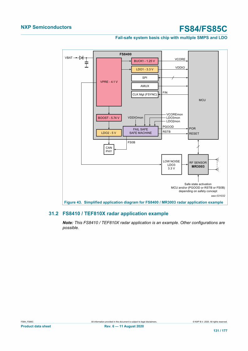
NXP Semiconductors FS84/FS85CFail-safe system basis chip with multiple SMPS and LDO
FS84_FS85C All information provided in this document is subject to legal disclaimers. © NXP B.V. 2020. All rights reserved.
Product data sheet Rev. 6 — 11 August 2020131 / 177
aaa-031032
VBATFS8400
BUCK1 - 1.25 V
LDO1 - 3.3 V
SPI
VCORE
VDDIO
AMUX
CLK Mgt (FSYNC)
VPRE - 4.1 V
MCU
RF SENSORMR3003
LOW NOISELDO33.3 V
Safe state activationMCU and/or (PGOOD or RSTB or FS0B)
depending on safety concept
LDO2 - 5 V
BOOST - 5.74 V
FAIL SAFESAFE MACHINE
VDDIOmonVCOREmonLDO3monLDO2mon
PGOOD
FIN
RSTBPOR
RESET
CANPHY
FS0B
Figure 43. Simplified application diagram for FS8400 / MR3003 radar application example
31.2 FS8410 / TEF810X radar application exampleNote: This FS8410 / TEF810X radar application is an example. Other configurations arepossible.
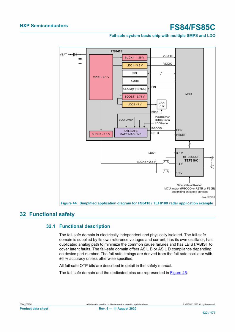
NXP Semiconductors FS84/FS85CFail-safe system basis chip with multiple SMPS and LDO
FS84_FS85C All information provided in this document is subject to legal disclaimers. © NXP B.V. 2020. All rights reserved.
Product data sheet Rev. 6 — 11 August 2020132 / 177
aaa-031033
VBATFS8410
BUCK1 - 1.25 V
LDO1 - 3.3 V
SPI
VCORE
VDDIO
AMUX
CLK Mgt (FSYNC)
BOOST - 5.74 V
VPRE - 4.1 V
MCU
RF SENSORTEF810X
Safe state activationMCU and/or (PGOOD or RSTB or FS0B)
depending on safety concept
BUCK3 - 2.3 VFAIL SAFE
SAFE MACHINE
VDDIOmonVCOREmonBUCK3monLDO2mon
PGOOD
FS0B
FIN
RSTB
LDO1
BUCK3 = 2.3 V
PORRESET
3.3 V
1.8 V
1.1 V
LDO2 - 5 V CANPHY
Figure 44. Simplified application diagram for FS8410 / TEF810X radar application example
32 Functional safety
32.1 Functional descriptionThe fail-safe domain is electrically independent and physically isolated. The fail-safedomain is supplied by its own reference voltages and current, has its own oscillator, hasduplicated analog path to minimize the common cause failures and has LBIST/ABIST tocover latent faults. The fail-safe domain offers ASIL B or ASIL D compliance dependingon device part number. The fail-safe timings are derived from the fail-safe oscillator with±6 % accuracy unless otherwise specified.
All fail-safe OTP bits are described in detail in the safety manual.
The fail-safe domain and the dedicated pins are represented in Figure 45:

NXP Semiconductors FS84/FS85CFail-safe system basis chip with multiple SMPS and LDO
FS84_FS85C All information provided in this document is subject to legal disclaimers. © NXP B.V. 2020. All rights reserved.
Product data sheet Rev. 6 — 11 August 2020133 / 177
aaa-031016
Vdig_FS OTPFail-Safe State Machine
ABISTLBIST Watchdog
MCU FailureMonitoring
(FCCU)
Ext. ICMonitoring
PGOODDriver
ResetDriver
Fail SafeOutput Driver
VoltageSupervision
VDDIO
Vdig_FS
VM
ON
1
VCOREMON
FCCU1
ERRMON
PGOOD
RSTB
FS0BFCCU2
VM
ON
2V
MO
N3
VM
ON
4
OSCFS
SPI/I2CFS
VMON1VMON2VMON3VMON4 BG2
Figure 45. Fail-safe block diagram
32.2 ASIL B versus ASIL D
Table 104. Recommended ASIL B vs ASIL D safety featuresSafety features ASIL B (FS84) ASIL D (FS85)
PGOOD output pin Yes Yes
RSTB output pin Yes Yes
FS0B output pin Yes Yes
VCORE voltage monitoring (VCOREMON) Yes Yes
VDDIO voltage monitoring Yes Yes
Voltage monitoring (VMONx) 2 to 4 up to 4
Watchdog monitoring Simple WD Challenger WD
FCCU monitoring Optional Yes
MCU fault recovery strategy No Yes
External IC monitoring (ERRMON) No Yes
Analog BIST (ABIST) Yes Yes
Logical BIST (LBIST) No Yes
32.3 Fail-safe initializationAfter POR or wake up from Standby, when the RSTB pin is released, the fail-safe statemachine enters in INIT_FS phase for initialization. To secure the writing process duringINIT_FS phase, in addition to CRC computation during SPI/I2C transfer, it is requestedfor the MCU to perform the following sequence for all INIT_FS registers:
1 - Write the desired data in the FS_I_Register_A (DATA)
2 - Write the opposite in the FS_I_NOT_Register_A (DATA_NOT)
As an example, if the data of FS_I_Register_A = 0xABCD, the data not ofFS_I_NOT_Register_A = 0x5432. A real-time comparison process (XOR) isperformed by the FS85/FS84 to ensure DATA FS_I_Register_A = DATA_NOTFS_I_NOT_Register_A. Only the utility bits must be inverted in the DATA_NOT content.The RESERVED bits are not considered and can be written at ‘0’. If the comparison

NXP Semiconductors FS84/FS85CFail-safe system basis chip with multiple SMPS and LDO
FS84_FS85C All information provided in this document is subject to legal disclaimers. © NXP B.V. 2020. All rights reserved.
Product data sheet Rev. 6 — 11 August 2020134 / 177
result is correct, then the REG_CORRUPT is set to ‘0’. If the comparison result is wrong,then the REG_CORRUPT bit is set to ‘1’. The REG_CORRUPT monitoring is active assoon as the INIT_FS is closed by the first good watchdog refresh.
INIT_FS must be closed by the first good watchdog refresh before 256 ms timeout.
After INIT_FS closure, it is possible to come back to INIT_FS with the GoTo_INITFS bitin FS_SAFE_IOS register, from any FS_state after INIT_FS. It is recommended to sendthe GoTo_INITFS command just after a good watchdog refresh.
32.4 WatchdogThe watchdog is a windowed watchdog for the Simple and the Challenger watchdog.The first half of the window is said CLOSED and the second half is said OPEN. A goodwatchdog refresh is a good watchdog answer during the OPEN window. A bad watchdogrefresh is a bad watchdog answer during the OPEN window, no watchdog refresh duringthe OPEN window or a good watchdog answer during the CLOSED window. After a goodor a bad watchdog refresh, a new window period starts immediately for the MCU to keepthe synchronization with the windowed watchdog.
The first good watchdog refresh closes the INIT_FS. Then the watchdog window isrunning and the MCU must refresh the watchdog in the OPEN window of the watchdogwindow period. The duration of the watchdog window is configurable from 1.0 ms to 1024ms with the WDW_PERIOD [3:0] bits. The new watchdog window is effective after thenext watchdog refresh. The watchdog window can be disabled during INIT_FS only. Thewatchdog disable is effective when the INIT_FS is closed.
The watchdog configuration requires to write in FS_WD_WINDOW andFS_NOT_WD_WINDOW registers like INIT registers.

NXP Semiconductors FS84/FS85CFail-safe system basis chip with multiple SMPS and LDO
FS84_FS85C All information provided in this document is subject to legal disclaimers. © NXP B.V. 2020. All rights reserved.
Product data sheet Rev. 6 — 11 August 2020135 / 177
Table 105. Watchdog window period configurationWDW_PERIOD [3:0] Watchdog window period
0000 DISABLE (during INIT_FS only)
0001 1.0 ms
0010 2.0 ms
0011 (default) 3.0 ms
0100 4.0 ms
0101 6.0 ms
0110 8.0 ms
0111 12 ms
1000 16 ms
1001 24 ms
1010 32 ms
1011 64 ms
1100 128 ms
1101 256 ms
1110 512 ms
1111 1024 ms
Reset condition POR
The duty cycle of the watchdog window is configurable from 31.25 % to 68.75 % with theWDW_DC [2:0] bits. The new duty cycle is effective after the next watchdog refresh.
Table 106. Watchdog window duty cycle configurationWDW_DC [2:0] CLOSED window OPEN window
000 31.25 % 68.75 %
001 37.5 % 62.5 %
010 (default) 50 % 50 %
011 62.5 % 37.5 %
100 68.75 % 31.25 %
Others 50 % 50 %
Reset condition POR
32.4.1 Challenger watchdog
The Challenger watchdog monitoring feature is enabled by OTP_WD_SELECTIONbit. The Challenger watchdog is based on a question/answer process with the MCU.A 16-bits pseudo-random word is generated by implementing a Linear Feedback ShiftRegister (LFSR) in the FS85. The MCU can send the seed of the LFSR or use the LFSRgenerated by the FS85 during the INIT_FS phase and performs a pre-defined calculation.The result is sent through the SPI/I2C during the OPEN watchdog window and verified bythe FS85. When the result is right, the watchdog window is restarted and a new LFSR is

NXP Semiconductors FS84/FS85CFail-safe system basis chip with multiple SMPS and LDO
FS84_FS85C All information provided in this document is subject to legal disclaimers. © NXP B.V. 2020. All rights reserved.
Product data sheet Rev. 6 — 11 August 2020136 / 177
generated. When the result is wrong, the WD error counter is incremented, the watchdogwindow is restarted and the LFSR value is not changed.
During the initialization phase (INIT_FS), the MCU sends the seed for the LFSR, or usesthe default LFSR value generated by the FS85 (0x5AB2), available in the WD_SEEDregister. Using this LFSR, the MCU performs a simple calculation based on belowformula and sends the results in the WD_ANSWER register.
aaa-031017
WD_SEED[23:8]
4 4 46
WD_ANSWER[23:8]X NOT /+ -
Figure 46. Challenger watchdog formula
In Challenger watchdog configuration, it is impossible to write 0x0000 in WD_SEEDregister. A communication error is reported in case of 0x0000 write tentative and theconfiguration is ignored.
32.4.2 Simple watchdog
The Simple watchdog monitoring feature is enabled by OTP_WD_SELECTIONbit. The Simple watchdog uses a unique seed. The MCU can send its own seed inWD_SEED register or uses the default value 0x5AB2. This seed must be written in theWD_ANSWER register during the OPEN watchdog window. When the result is right,the watchdog window is restarted. When the result is wrong, the WD error counter isincremented and the watchdog window is restarted. In Simple watchdog configuration, itis impossible to write 0xFFFF and 0x0000 in WD_SEED register. A communication erroris reported in case of 0x0000 and 0xFFFF write tentative and the configuration is ignored.
32.4.3 Watchdog error counter
The watchdog error strategy is available for the Challenger watchdog and the Simplewatchdog. The watchdog error counter is implemented in the device to filter the incorrectwatchdog refresh. Each time a watchdog failure occurs, the device increments thiscounter by 2. The watchdog error counter is decremented by 1 each time the watchdogis properly refreshed. This principle ensures a cyclic ’OK/NOK’ behavior converges to afailure detection.
To allow flexibility in the application, the maximum value of this counter is configurablewith the WD_ERR_LIMIT[1:0] bits during the INIT_FS phase.
Table 107. Watchdog error counter configurationWD_ERR_LIMIT[1:0] Watchdog error counter value
00 8
01 (default) 6
10 4
11 2
Reset condition POR
The watchdog error counter value can be read by the MCU for diagnostic with theWD_ERR_CNT[3:0] bits.

NXP Semiconductors FS84/FS85CFail-safe system basis chip with multiple SMPS and LDO
FS84_FS85C All information provided in this document is subject to legal disclaimers. © NXP B.V. 2020. All rights reserved.
Product data sheet Rev. 6 — 11 August 2020137 / 177
aaa-031018
WD_ERR_LIMIT = 11
WD_ERR_LIMIT = 10
WD_ERR_LIMIT = 01
00
1
2
3
4
WD refreshNOT OK
WD refresh OK
WD refresh OK
WD refresh OK
WD refresh OK
WD refresh OK
WD refresh OK
WD refresh OK
WD refresh OK
WD refreshNOT OK
WD refreshNOT OK
WD refreshNOT OK
0
1
2
3
4
5
6
WD refreshNOT OK
WD refreshNOT OK
WD refreshNOT OK
WD refreshNOT OK
WD refreshNOT OK
WD refreshNOT OK
WD refresh OK
2
1
WD OFFWD refresh OKWD OFFWD refresh OKWD OFF
WD_ERR_LIMIT = 00
WD refresh OK
WD refresh OK
WD refresh OK
WD refresh OK
WD refresh OK
0
1
2
3
4
5
6
WD refresh OK
WD refreshNOT OK
WD refreshNOT OK
WD refreshNOT OK
WD refresh OK
7
8
WD refreshNOT OK
WD refreshNOT OK
WD refreshNOT OK
WD refreshNOT OK
WD refresh OKWD OFF
WD refreshNOT OK
WD refreshNOT OK
Figure 47. Watchdog error counter configurations
32.4.4 Watchdog refresh counter
The watchdog refresh strategy is available for the Challenger watchdog and theSimple watchdog. The watchdog refresh counter is used to decrement the fault errorcounter. Each time the watchdog is properly refreshed, the watchdog refresh counter isincremented by ’1’. Each time the watchdog refresh counter reaches its maximum value(‘6’ by default) and if next WD refresh is also good, the fault error counter is decrementedby ’1’. Whatever the position the watchdog refresh counter is in, each time there is awrong refresh watchdog, the watchdog refresh counter is reset to ’0’.
To allow flexibility in the application, the maximum value of this watchdog refresh counteris configurable with the WD_RFR_LIMIT[1:0] bits during the INIT_FS phase.
Table 108. Watchdog refresh counter configurationWD_RFR_LIMIT[1:0] Watchdog refresh counter value
00 (default) 6
01 4
10 2
11 1
Reset condition POR
The watchdog refresh counter value can be read by the MCU for diagnostic with theWD_RFR_CNT[2:0] bits.
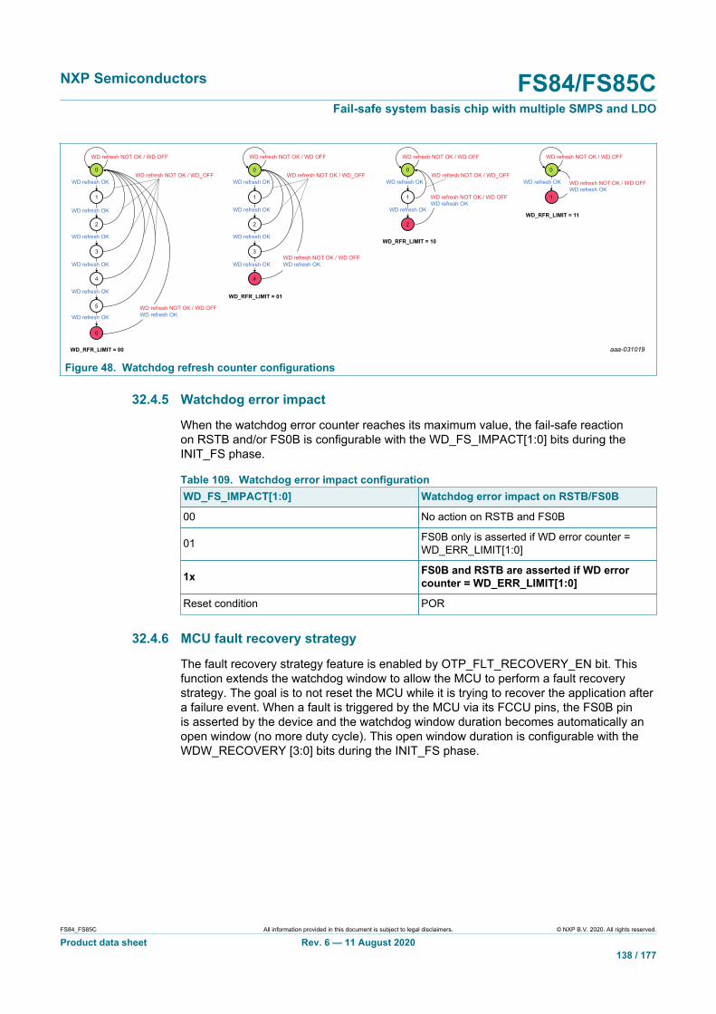
NXP Semiconductors FS84/FS85CFail-safe system basis chip with multiple SMPS and LDO
FS84_FS85C All information provided in this document is subject to legal disclaimers. © NXP B.V. 2020. All rights reserved.
Product data sheet Rev. 6 — 11 August 2020138 / 177
WD refresh NOT OK / WD OFFWD refresh OK
WD refresh NOT OK / WD OFFWD refresh OK
WD refresh NOT OK / WD OFFWD refresh OK
WD refresh NOT OK / WD OFFWD refresh OK
WD refresh OK
WD refresh OK
WD refresh OK
WD refresh OK
WD refresh OK
0
1
2
3
4
5
6
WD refresh OK
aaa-031019
WD refresh NOT OK / WD OFF
WD refresh NOT OK / WD_OFF WD refresh NOT OK / WD_OFF WD refresh NOT OK / WD_OFF
WD refresh OK
WD refresh OK
WD refresh OK
WD refresh OK
0
1
2
3
4
WD refresh NOT OK / WD OFF
WD refresh OK
WD refresh OK
0
1
2
WD refresh NOT OK / WD OFF
WD refresh OK
0
1
WD refresh NOT OK / WD OFF
WD_RFR_LIMIT = 00
WD_RFR_LIMIT = 01
WD_RFR_LIMIT = 10
WD_RFR_LIMIT = 11
Figure 48. Watchdog refresh counter configurations
32.4.5 Watchdog error impact
When the watchdog error counter reaches its maximum value, the fail-safe reactionon RSTB and/or FS0B is configurable with the WD_FS_IMPACT[1:0] bits during theINIT_FS phase.
Table 109. Watchdog error impact configurationWD_FS_IMPACT[1:0] Watchdog error impact on RSTB/FS0B
00 No action on RSTB and FS0B
01 FS0B only is asserted if WD error counter =WD_ERR_LIMIT[1:0]
1x FS0B and RSTB are asserted if WD errorcounter = WD_ERR_LIMIT[1:0]
Reset condition POR
32.4.6 MCU fault recovery strategy
The fault recovery strategy feature is enabled by OTP_FLT_RECOVERY_EN bit. Thisfunction extends the watchdog window to allow the MCU to perform a fault recoverystrategy. The goal is to not reset the MCU while it is trying to recover the application aftera failure event. When a fault is triggered by the MCU via its FCCU pins, the FS0B pinis asserted by the device and the watchdog window duration becomes automatically anopen window (no more duty cycle). This open window duration is configurable with theWDW_RECOVERY [3:0] bits during the INIT_FS phase.
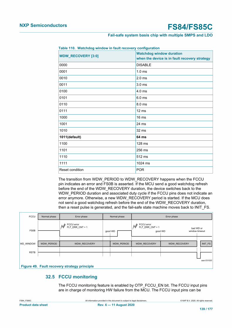
NXP Semiconductors FS84/FS85CFail-safe system basis chip with multiple SMPS and LDO
FS84_FS85C All information provided in this document is subject to legal disclaimers. © NXP B.V. 2020. All rights reserved.
Product data sheet Rev. 6 — 11 August 2020139 / 177
Table 110. Watchdog window in fault recovery configuration
WDW_RECOVERY [3:0] Watchdog window durationwhen the device is in fault recovery strategy
0000 DISABLE
0001 1.0 ms
0010 2.0 ms
0011 3.0 ms
0100 4.0 ms
0101 6.0 ms
0110 8.0 ms
0111 12 ms
1000 16 ms
1001 24 ms
1010 32 ms
1011(default) 64 ms
1100 128 ms
1101 256 ms
1110 512 ms
1111 1024 ms
Reset condition POR
The transition from WDW_PERIOD to WDW_RECOVERY happens when the FCCUpin indicates an error and FS0B is asserted. If the MCU send a good watchdog refreshbefore the end of the WDW_RECOVERY duration, the device switches back to theWDW_PERIOD duration and associated duty cycle if the FCCU pins does not indicate anerror anymore. Otherwise, a new WDW_RECOVERY period is started. If the MCU doesnot send a good watchdog refresh before the end of the WDW_RECOVERY duration,then a reset pulse is generated, and the fail-safe state machine moves back to INIT_FS.
aaa-031020
Normal phaseFCCU Normal phaseError phase Error phase
WDW_PERIODWD_WINDOW
FS0B
RSTB
WDW_PERIOD
good WD
FCCU errorFLT_ERR_CNT + 1
FCCU errorFLT_ERR_CNT + 1
good WDbad WD or
window timeout
WDW_RECOVERY WDW_RECOVERY INIT_FSWDW_RECOVERY
Figure 49. Fault recovery strategy principle
32.5 FCCU monitoringThe FCCU monitoring feature is enabled by OTP_FCCU_EN bit. The FCCU input pinsare in charge of monitoring HW failure from the MCU. The FCCU input pins can be

NXP Semiconductors FS84/FS85CFail-safe system basis chip with multiple SMPS and LDO
FS84_FS85C All information provided in this document is subject to legal disclaimers. © NXP B.V. 2020. All rights reserved.
Product data sheet Rev. 6 — 11 August 2020140 / 177
configured by pair, or single independent inputs. The FCCU monitoring is active as soonas the INIT_FS is closed by the first good watchdog refresh. The FCCU input pins areconfigured by pair, or single independent inputs with the FCCU_CFG[1:0] bits.
Table 111. FCCU pins configurationFCCU_CFG[1:0] FCCU pins configuration
00 No monitoring
01 (default) FCCU1 and FCCU2 monitoring by pair (bi-stable protocol)
10 FCCU1 or FCCU2 input monitoring
11 FCCU1 input monitoring only
Reset condition POR
32.5.1 FCCU12 monitoring by pair
When FCCU12 are used by pair, the bi-stable protocol is supported according toFigure 50:
aaa-031021
FCCU1
Reset phase Normal phase Error phase Config. phase
FCCU2
Figure 50. FCCU bi-stable protocol
The polarity of the FCCU fault signals is configurable with FCCU12_FLT_POL bit duringthe INIT_FS phase.
Table 112. FCCU12 polarity configurationFCCU12_FLT_POL FCCU12 polarity
0 (default) FCCU1=0 or FCCU2=1 level is a fault
1 FCCU1=1 or FCCU2=0 level is a fault
Reset condition POR
When FCCU fault is detected, the fail-safe reaction on RSTB and/or FS0B is configurablewith the FCCU12_FS_IMPACT bit during the INIT_FS phase
Table 113. FCCU12 error impact configurationFCCU12_FS_IMPACT FCCU12 impact on RSTB/FS0B
0 FS0B only is asserted
1 (default) FS0B and RSTB are asserted
Reset condition POR
NXP Semiconductors FS84/FS85CFail-safe system basis chip with multiple SMPS and LDO
FS84_FS85C All information provided in this document is subject to legal disclaimers. © NXP B.V. 2020. All rights reserved.
Product data sheet Rev. 6 — 11 August 2020141 / 177
32.5.2 FCCU12 independent monitoring
When FCCU1 and/or FCCU2 are used independently, the FCCU inputs can monitor twodifferent and independent error signals. For each input the polarity of the FCCU faultsignal is configurable with FCCUx_FLT_POL bits during the INIT_FS phase.
Table 114. FCCUx polarity configurationFCCU1_FLT_POL FCCU1 polarity
0 (default) FCCU1 low level is a fault
1 FCCU1 high level is a fault
Reset condition POR
FCCU2_FLT_POL FCCU2 polarity
0 (default) FCCU2 low level is a fault
1 FCCU2 high level is a fault
Reset condition POR
When FCCU fault is detected, the fail-safe reaction on RSTB and/or FS0B is configurablewith the FCCUx_FS_IMPACT bits during the INIT_FS phase.
Table 115. FCCUx error impact configurationFCCU1_FS_IMPACT FCCU1 impact on RSTB/FS0B
0 FS0B only is asserted
1 (default) FS0B and RSTB are asserted
Reset condition POR
FCCU2_FS_IMPACT FCCU2 impact on RSTB/FS0B
0 FS0B only is asserted
1 (default) FS0B and RSTB are asserted
Reset condition POR

NXP Semiconductors FS84/FS85CFail-safe system basis chip with multiple SMPS and LDO
FS84_FS85C All information provided in this document is subject to legal disclaimers. © NXP B.V. 2020. All rights reserved.
Product data sheet Rev. 6 — 11 August 2020142 / 177
32.5.3 FCCU12 electrical characteristics
Table 116. Electrical characteristicsTA = −40 °C to 125 °C, unless otherwise specified. VSUP = VSUP_UVH to 36 V, unless otherwise specified. All voltagesreferenced to ground.
Symbol Parameter Min Typ Max Unit
FCCU1,2
FCCU12TERR FCCU1,2 filtering time 4.0 — 8.0 μs
FCCU12VIH FCCU1,2 high level input voltage threshold — — 0.7 x VDDIO V
FCCU12VIL FCCU1,2 low level input voltage threshold 0.3 x VDDIO — — V
FCCU12HYST FCCU1,2 input voltage hysteresis 0.1 x VDDIO — 1.85 V
FCCU12ILKG Input leakage current — — 1.0 μA
FCCU1RPD FCCU1 internal pull down resistor 400 800 1300 kΩ
FCCU2RPU FCCU2 internal pull up resistor to VDDIO 100 200 400 kΩ
FCCU12RATIOFCCU1/2 internal resistor ratio (FCCU1RPD /FCCU2RPU) 3.5 4 4.5 —
32.6 Voltage supervisorThe voltage supervisor is in charge of overvoltage and undervoltage monitoring ofVCOREMON, VDDIO and VMONx input pins. When an overvoltage occurs on a FS85/FS84 regulator monitored by one of these pins, the associated FS85/FS84 regulatoris switched off till the fault is removed. The voltage monitoring is active as soon asFS_ENABLE=1 and UV/OV flags are then reported accordingly.
32.6.1 VCOREMON monitoring
VCOREMON input pin is dedicated to BUCK1 or BUCK1 and BUCK2 in case ofmultiphase operation. When overvoltage or undervoltage fault is detected, the fail-safe reaction on RSTB and/or FS0B is configurable with the VCOREMON_OV/UV_FS_IMPACT[1:0] bits during the INIT_FS phase.
Table 117. VCOREMON error impact configurationVCOREMON_OV_FS_IMPACT[1:0] VCOREMON OV impact on RSTB/FS0B
00 No effect on RSTB and FS0B
01 FS0B only is asserted
1x (default) FS0B and RSTB are asserted
Reset condition POR
VCOREMON_UV_FS_IMPACT[1:0] VCOREMON UV impact on RSTB/FS0B
00 No effect on RSTB and FS0B
01 (default) FS0B only is asserted
1x FS0B and RSTB are asserted
Reset condition POR

NXP Semiconductors FS84/FS85CFail-safe system basis chip with multiple SMPS and LDO
FS84_FS85C All information provided in this document is subject to legal disclaimers. © NXP B.V. 2020. All rights reserved.
Product data sheet Rev. 6 — 11 August 2020143 / 177
Table 118. Electrical characteristicsTA = −40 °C to 125 °C, unless otherwise specified. VSUP = VSUP_UVH to 36 V, unless otherwise specified. All voltagesreferenced to ground.
Symbol Parameter Min Typ Max Unit
VCOREMON
VCOREMON_OV_min Overvoltage threshold minimum — +4.5 — %
VCOREMON_OV_max Overvoltage threshold maximum — +12 — %
VCOREMON_OV_step Overvoltage threshold step (OTP_VCOREOVTH[7:0] bits) — +0.5 — %
VCOREMON_OV_acc Overvoltage threshold accuracy −2 — 2 %
20 25 30 μsTCOREMON_OV Overvoltage filtering time (OTP_VCORE_OV_
DGLT bit) 40 45 50 μs
VCOREMON_UV_min Undervoltage threshold minimum — −4.5 — %
VCOREMON_UV_max Undervoltage threshold maximum — −12 — %
VCOREMON_UV_step Undervoltage threshold step (OTP_VCOREUVTH[7:0] bits) — −0.5 — %
VCOREMON_UV_acc Undervoltage threshold accuracy −2 — 2 %
2.5 5 7.5 μs
10 15 20 μs
20 25 30 μsTCOREMON_UV Undervoltage filtering time (OTP_VCORE_UV_
DGLT[1:0] bits)
35 40 45 μs
32.6.2 Static voltage scaling (SVS)
A static voltage scaling function is implemented to allow the MCU to reduce the outputvoltage initially configured at start-up of BUCK1 (and BUCK2 if used in multiphase). TheSVS configuration must be done in INIT_FS phase. The offset value is configurable bySPI/I2C with the SVS_OFFSET[4:0] bits and the exact complemented value shall bewritten in the NOT_SVS_OFFSET[4:0] bits.
Table 119. SVS offset configuration
SVS_OFFSET[4:0] NOT_SVS_OFFSET[4:0]Offset applied to BUCK1(and BUCK2 if used inmultiphase)
00000 (default) 11111 0 mV
00001 11110 −6.25 mV
- - - - - - - - - - −6.25 mV step per bit
10000 01111 −100 mV
Reset condition POR
The BUCK1/2 output voltage transition starts when the NOT_SVS_OFFSET[4:0] SPI/I2C command is received and confirmed good. If the NOT_SVS_OFFSET[4:0] SPI/I2Ccommand is not the exact opposite to the SVS_OFFSET[4:0] SPI/I2C command, theSVS procedure is not executed and the BUCK1 output voltage remains at its originalvalue. The OV/UV threshold changes immediately when the NOT_SVS_OFFSET[4:0]SPI/I2C command is received and confirmed good. The BUCK1 output voltage transitionlast less than TCOREMON_OV, preventing a false OV detection.

NXP Semiconductors FS84/FS85CFail-safe system basis chip with multiple SMPS and LDO
FS84_FS85C All information provided in this document is subject to legal disclaimers. © NXP B.V. 2020. All rights reserved.
Product data sheet Rev. 6 — 11 August 2020144 / 177
aaa-031022
OV
UV
TCOREMON_OV
VBUCK1 = VCOREMON = 0.75 V
VBUCK1 = VCOREMON = 0.8 V
SPI/I2CFS_I_NOT_SVS
SPI/I2CFS_I_SVS
VBUCK12_SVS
Figure 51. SVS principle
32.6.3 VDDIO monitoring
VDDIO input pin can be connected to VPRE, LDO1, LDO2, BUCK3 or an externalregulator. The regulator connected to VDDIO must be at 3.3 V or 5.0 V to be compatiblewith overvoltage and undervoltage monitoring thresholds. In order to turn OFF theregulator in case of overvoltage detection, the configuration of which regulator isconnected to VDDIO is done with OTP_VDDIO_REG_ASSIGN[2:0] bits. If an externalregulator (not delivered by the FS85/FS84) is connected to VDDIO, this regulatorcannot be turned OFF, but the overvoltage flag is reported to the MCU which can takeappropriate action. In all cases, the fail-safe reaction on RSTB and/or FS0B configuredwith VDDIO_OV/UV_FS_IMPACT[1:0] bits is guaranteed.
aaa-031023
UV
bandgap_FS
OTP_VDDIOOVTH[3:0]OTP_VDDIOUVTH[3:0]
OTP_VDDIO_V
VDDIO
OV
Figure 52. VDDIO monitoring principle
When overvoltage or undervoltage fault is detected, the fail-safe reaction on RSTB and/or FS0B is configurable with the VDDIO_OV/UV_IMPACT[1:0] bits during the INIT_FSphase.

NXP Semiconductors FS84/FS85CFail-safe system basis chip with multiple SMPS and LDO
FS84_FS85C All information provided in this document is subject to legal disclaimers. © NXP B.V. 2020. All rights reserved.
Product data sheet Rev. 6 — 11 August 2020145 / 177
Table 120. VDDIO error impact configurationVDDIO_OV_FS_IMPACT[1:0] VDDIO OV impact on RSTB/FS0B
00 No effect on RSTB and FS0B
01 FS0B only is asserted
1x (default) FS0B and RSTB are asserted
Reset condition POR
VDDIO_UV_FS_IMPACT[1:0] VDDIO UV impact on RSTB/FS0B
00 No effect on RSTB and FS0B
01 (default) FS0B only is asserted
1x FS0B and RSTB are asserted
Reset condition POR
Table 121. Electrical characteristicsTA = −40 °C to 125 °C, unless otherwise specified. VSUP = VSUP_UVH to 36 V, unless otherwise specified. All voltagesreferenced to ground.
Symbol Parameter Min Typ Max Unit
VDDIO
VDDIO_OV_min Overvoltage threshold minimum — +4.5 — %
VDDIO_OV_max Overvoltage threshold maximum — +12 — %
VDDIO_OV_step Overvoltage threshold step (OTP_VDDIOOVTH[7:0] bits) — +0.5 — %
VDDIO_OV_acc Overvoltage threshold accuracy −2 — 2 %
20 25 30 μsTVDDIO_OV Overvoltage filtering time (OTP_VDDIO_OV_
DGLT bit) 40 45 50 μs
VDDIO_UV_min Undervoltage threshold minimum — −4.5 — %
VDDIO_UV_max Undervoltage threshold maximum — −12 — %
VDDIO_UV_step Undervoltage threshold step (OTP_VDDIOUVTH[7:0] bits) — −0.5 — %
VDDIO_UV_acc Undervoltage threshold accuracy −2 — 2 %
2.5 5 7.5 μs
10 15 20 μs
20 25 30 μsTVDDIO_UV Undervoltage filtering time (OTP_VDDIO_UV_
DGLT[1:0] bits)
35 40 45 μs
32.6.4 VMONx monitoring
Each VMONx monitoring feature is enabled by OTP. VMONx input pin can be connectedto VPRE, LDO1, LDO2, BUCK3, BUCK2 (in case BUCK2 is not used in multiphase) oreven an external regulator. In order to turn OFF the regulator in case of Overvoltagedetection, the configuration of which regulator is connected to VMONx is done by SPI/I2C in the register M_VMON_REGx. If an external regulator (not delivered by the FS85/FS84) is connected to VMONx, this regulator cannot be turned OFF, but the Overvoltageflag is reported to the MCU which can take appropriate action. In all cases, the fail-safe
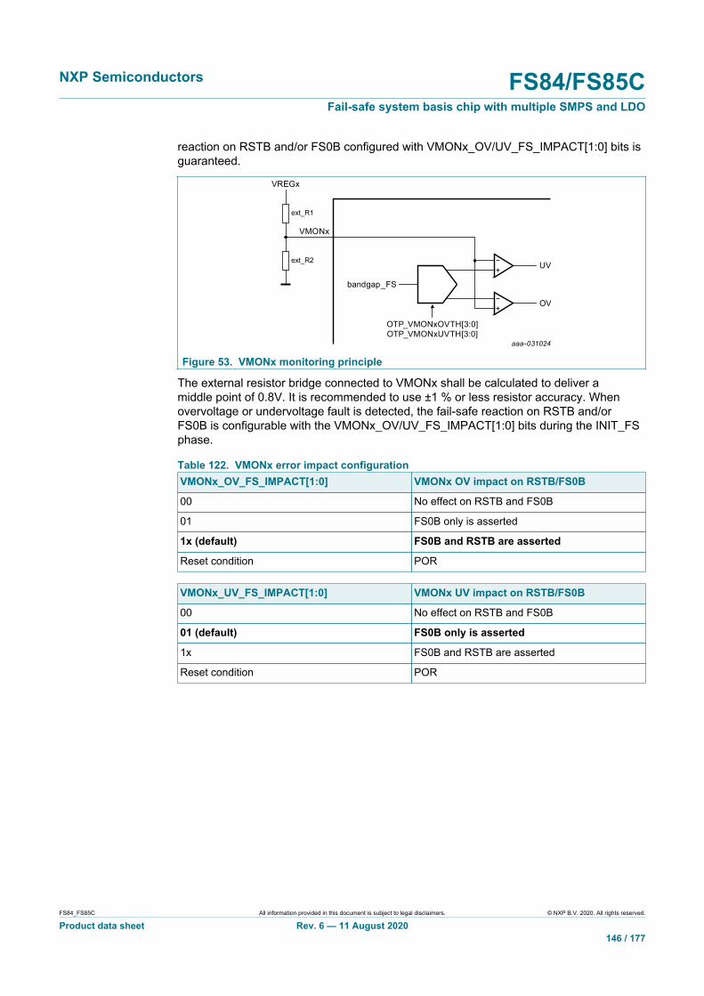
NXP Semiconductors FS84/FS85CFail-safe system basis chip with multiple SMPS and LDO
FS84_FS85C All information provided in this document is subject to legal disclaimers. © NXP B.V. 2020. All rights reserved.
Product data sheet Rev. 6 — 11 August 2020146 / 177
reaction on RSTB and/or FS0B configured with VMONx_OV/UV_FS_IMPACT[1:0] bits isguaranteed.
aaa-031024
UV
bandgap_FS
OTP_VMONxOVTH[3:0]OTP_VMONxUVTH[3:0]
ext_R1
ext_R2
VREGx
VMONx
OV
Figure 53. VMONx monitoring principle
The external resistor bridge connected to VMONx shall be calculated to deliver amiddle point of 0.8V. It is recommended to use ±1 % or less resistor accuracy. Whenovervoltage or undervoltage fault is detected, the fail-safe reaction on RSTB and/orFS0B is configurable with the VMONx_OV/UV_FS_IMPACT[1:0] bits during the INIT_FSphase.
Table 122. VMONx error impact configurationVMONx_OV_FS_IMPACT[1:0] VMONx OV impact on RSTB/FS0B
00 No effect on RSTB and FS0B
01 FS0B only is asserted
1x (default) FS0B and RSTB are asserted
Reset condition POR
VMONx_UV_FS_IMPACT[1:0] VMONx UV impact on RSTB/FS0B
00 No effect on RSTB and FS0B
01 (default) FS0B only is asserted
1x FS0B and RSTB are asserted
Reset condition POR
NXP Semiconductors FS84/FS85CFail-safe system basis chip with multiple SMPS and LDO
FS84_FS85C All information provided in this document is subject to legal disclaimers. © NXP B.V. 2020. All rights reserved.
Product data sheet Rev. 6 — 11 August 2020147 / 177
Table 123. Electrical characteristicsTA = −40 °C to 125 °C, unless otherwise specified. VSUP = VSUP_UVH to 36 V, unless otherwise specified. All voltagesreferenced to ground.
Symbol Parameter Min Typ Max Unit
VMONx (without ext resistor accuracy)
VMONx_OV_min Overvoltage threshold minimum — +4.5 — %
VMONx_OV_max Overvoltage threshold maximum — +12 — %
VMONx_OV_step Overvoltage threshold step (OTP_VMONxOVTH[7:0] bits) — +0.5 — %
VMONx_OV_acc Overvoltage threshold accuracy −2 — 2 %
20 25 30 μsTMONx_OV Overvoltage filtering time (OTP_
VMONx_OV_DGLT bit) 40 45 50 μs
VMONx_UV_min Undervoltage threshold minimum — −4.5 — %
VMONx_UV_max Undervoltage threshold maximum — −12 — %
VMONx_UV_step Undervoltage threshold step (OTP_VMONxUVTH[7:0] bits) — −0.5 — %
VMONx_UV_acc Undervoltage threshold accuracy −2 — 2 %
2.5 5 7.5 μs
10 15 20 μs
20 25 30 μsTMONx_UV Undervoltage filtering time (OTP_
VMONx_UV_DGLT[1:0] bits)
35 40 45 μs
VMONx_PD Internal passive pull down 1 2 4 MΩ
32.7 External IC monitoring (ERRMON)The external IC monitoring feature is enabled by OTP_ERRMON_EN bit. The ERRMONinput pin is in charge to monitor an external IC on the application, neither the FS85, northe MCU. The ERRMON monitoring is active as soon as the INIT_FS is closed by thefirst good watchdog refresh
A transition detected at ERRMON pin indicates an error from the external IC. The polarityof the ERRMON fault signal is configurable with ERRMON_FLT_POL bit during theINIT_FS phase.
Table 124. ERRMON polarity configurationERRMON_FLT_POL ERRMON polarity
0 (default) Negative edge at ERRMON pin is a fault
1 Positive edge at ERRMON pin is a fault
Reset condition POR
The acknowledge timing from the MCU is configurable with theERRMON_ACK_TIME[1:0] bits.

NXP Semiconductors FS84/FS85CFail-safe system basis chip with multiple SMPS and LDO
FS84_FS85C All information provided in this document is subject to legal disclaimers. © NXP B.V. 2020. All rights reserved.
Product data sheet Rev. 6 — 11 August 2020148 / 177
Table 125. ERRMON timing configurationERRMON_ACK_TIME[1:0] ERRMON acknowledgement timing
00 1 ms
01 (default) 8 ms
10 16 ms
11 32 ms
Reset condition POR
The acknowledgement by the MCU is done through SPI/I2C communication according toFigure 54.
FS85/FS84 internalmonitoring signal
latched
Error signal(ERRMON input)
Acknowledgment counter
Resetcounter
Restart acknowledgmentcounter
FS0B
Error acknowledged by MCUInternal monitoring signal released
No error reportedError NOT acknowledged by MCU
Error reported at the end of the counterFS0B is asserted
aaa-031025
Figure 54. ERRMON principle
When ERRMON fault is detected, the fail-safe reaction on RSTB and/or FS0B isconfigurable with the ERRMON_FS_IMPACT bit during the INIT_FS phase.
Table 126. ERRMON error impact configurationERRMON_FS_IMPACT ERRMON impact on RSTB/FS0B
0 FS0B only is asserted when ERRMON fault isdetected
1 (default) FS0B and RSTB are asserted when ERRMONfault is detected
Reset condition POR

NXP Semiconductors FS84/FS85CFail-safe system basis chip with multiple SMPS and LDO
FS84_FS85C All information provided in this document is subject to legal disclaimers. © NXP B.V. 2020. All rights reserved.
Product data sheet Rev. 6 — 11 August 2020149 / 177
Table 127. Electrical characteristicsTA = −40 °C to 125 °C, unless otherwise specified. VSUP = VSUP_UVH to 36 V, unless otherwise specified. All voltagesreferenced to ground.
Symbol Parameter Min Typ Max Unit
ERRMON
ERRMONTACK_ACC Acknowledgement counter accuracy −10 — 10 %
ERRMONTERR Filtering time 4.0 — 8.0 μs
ERRMONVIH High level input voltage threshold — — 2.0 V
ERRMONVIL Low level input voltage threshold 1.0 — — V
ERRMONHYST Input voltage hysteresis 100 — 500 mV
ERRMONIPD Internal pull down current source 7 10 13 μA
32.8 Fault management
32.8.1 Fault error counter
The FS85/FS84 integrates a configurable fault error counter which is counting thenumber of faults related to the device itself and also caused by external events. The faulterror counter starts at level "1" after a POR or resuming from Standby. The final valueof the fault error counter is used to transition in DEEP-FS mode. The maximum value ofthis counter is configurable with the FLT_ERR_CNT_LIMIT[1:0] bits during the INIT_FSphase.
Table 128. Fault error counter configuration
FLT_ERR_CNT_LIMIT[1:0] Fault error counter maxvalue configuration
Fault error counterintermediate value
00 2 1
01 (default) 6 3
10 8 4
11 12 6
Reset condition POR
The fault error counter has two output values: intermediate and final. The intermediatevalue can be used to force the FS0B activation or generate a RSTB pulse according tothe FLT_ERR_IMPACT[1:0] bits configuration.
Table 129. Fault error counter impact configuration
FLT_ERR_IMPACT[1:0] Fault error counter intermediate value impact on RSTB/FS0B
00 No effect on RSTB and FS0B
01 FS0B only is asserted if FLT_ERR_CNT=intermediate value
1x (default)FS0B is asserted if FLT_ERR_CNT=intermediate valueRSTB is asserted for each value of FLT_ERR_CNT>=intermediate value
Reset condition POR
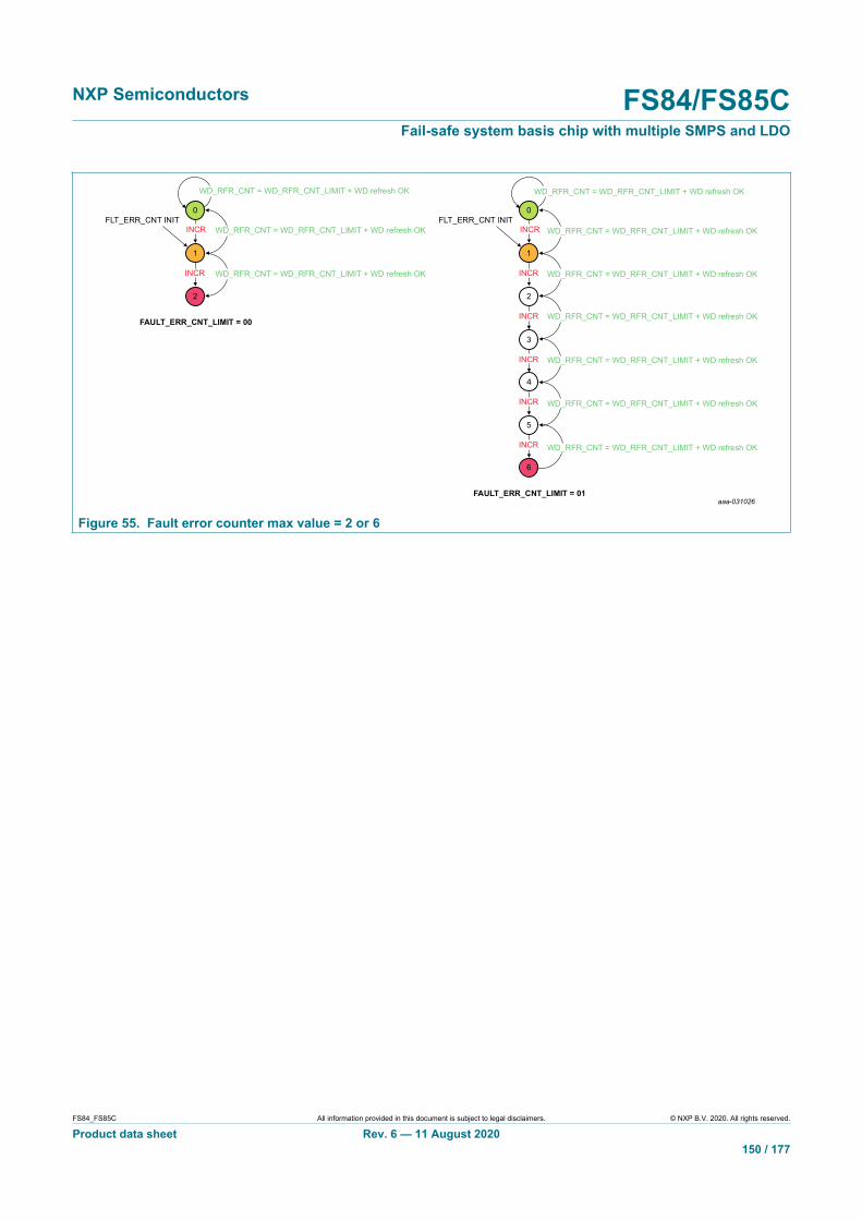
NXP Semiconductors FS84/FS85CFail-safe system basis chip with multiple SMPS and LDO
FS84_FS85C All information provided in this document is subject to legal disclaimers. © NXP B.V. 2020. All rights reserved.
Product data sheet Rev. 6 — 11 August 2020150 / 177
INCR
INCR
INCR
INCR
INCR
WD_RFR_CNT = WD_RFR_CNT_LIMIT + WD refresh OK
WD_RFR_CNT = WD_RFR_CNT_LIMIT + WD refresh OK
WD_RFR_CNT = WD_RFR_CNT_LIMIT + WD refresh OK
WD_RFR_CNT = WD_RFR_CNT_LIMIT + WD refresh OK
WD_RFR_CNT = WD_RFR_CNT_LIMIT + WD refresh OK
aaa-031026
1
6
INCR
WD_RFR_CNT = WD_RFR_CNT_LIMIT + WD refresh OK
WD_RFR_CNT = WD_RFR_CNT_LIMIT + WD refresh OK
FAULT_ERR_CNT_LIMIT = 01
2
3
5
4
0
INCR
1
FLT_ERR_CNT INITFLT_ERR_CNT INITINCR
WD_RFR_CNT = WD_RFR_CNT_LIMIT + WD refresh OK
WD_RFR_CNT = WD_RFR_CNT_LIMIT + WD refresh OK
WD_RFR_CNT = WD_RFR_CNT_LIMIT + WD refresh OK
FAULT_ERR_CNT_LIMIT = 00
2
0
Figure 55. Fault error counter max value = 2 or 6

NXP Semiconductors FS84/FS85CFail-safe system basis chip with multiple SMPS and LDO
FS84_FS85C All information provided in this document is subject to legal disclaimers. © NXP B.V. 2020. All rights reserved.
Product data sheet Rev. 6 — 11 August 2020151 / 177
INCR
INCR
INCR
INCR
INCR
WD_RFR_CNT = WD_RFR_CNT_LIMIT + WD refresh OK
WD_RFR_CNT = WD_RFR_CNT_LIMIT + WD refresh OK
WD_RFR_CNT = WD_RFR_CNT_LIMIT + WD refresh OK
WD_RFR_CNT = WD_RFR_CNT_LIMIT + WD refresh OK
WD_RFR_CNT = WD_RFR_CNT_LIMIT + WD refresh OK
aaa-031027
1
12
INCR
WD_RFR_CNT = WD_RFR_CNT_LIMIT + WD refresh OK
WD_RFR_CNT = WD_RFR_CNT_LIMIT + WD refresh OK
FAULT_ERR_CNT_LIMIT = 11
FAULT_ERR_CNT_LIMIT = 10
2
9
11
10
INCR
INCR
INCR
WD_RFR_CNT = WD_RFR_CNT_LIMIT + WD refresh OK
WD_RFR_CNT = WD_RFR_CNT_LIMIT + WD refresh OK
WD_RFR_CNT = WD_RFR_CNT_LIMIT + WD refresh OK
6
8
7
INCR
INCR
INCR
WD_RFR_CNT = WD_RFR_CNT_LIMIT + WD refresh OK
WD_RFR_CNT = WD_RFR_CNT_LIMIT + WD refresh OK
WD_RFR_CNT = WD_RFR_CNT_LIMIT + WD refresh OK
3
5
4
0FLT_ERR_CNT INIT
INCR WD_RFR_CNT = WD_RFR_CNT_LIMIT + WD refresh OK
1
INCR
WD_RFR_CNT = WD_RFR_CNT_LIMIT + WD refresh OK
WD_RFR_CNT = WD_RFR_CNT_LIMIT + WD refresh OK
2
INCR
INCR
INCR
WD_RFR_CNT = WD_RFR_CNT_LIMIT + WD refresh OK
WD_RFR_CNT = WD_RFR_CNT_LIMIT + WD refresh OK
WD_RFR_CNT = WD_RFR_CNT_LIMIT + WD refresh OK
6
8
7
INCR
INCR
INCR
WD_RFR_CNT = WD_RFR_CNT_LIMIT + WD refresh OK
WD_RFR_CNT = WD_RFR_CNT_LIMIT + WD refresh OK
WD_RFR_CNT = WD_RFR_CNT_LIMIT + WD refresh OK
3
5
4
0FLT_ERR_CNT INIT
Figure 56. Fault error counter max value = 8 or 12
32.8.2 Fault source and reaction
In normal operation when FS0B and RSTB are released, the fault error counteris incremented when a fault is detected by the FS85/FS84 fail-safe sate machine.Table 130 lists the faults and their impact on PGOOD, RSTB and FS0B pins accordingto the device configuration. The faults that are configured to not assert RSTB and FS0Bwill not increment the fault error counter. In that case, only the flags are available forMCU diagnostic. The fault error counter is incremented by 1, each time the RSTB and/or FS0B pin is asserted. When FS0B is asserted, the fault error counter continues to beincremented by +1 each time the WD error counter reach its maximum value.
NXP Semiconductors FS84/FS85CFail-safe system basis chip with multiple SMPS and LDO
FS84_FS85C All information provided in this document is subject to legal disclaimers. © NXP B.V. 2020. All rights reserved.
Product data sheet Rev. 6 — 11 August 2020152 / 177
Table 130. Application related fail-safe fault list and reactionIn Orange, the reaction in not configurable.In Green, the reaction is configurable by OTP for PGOOD and by SPI/I2C for RSTB/FS0B during INIT_FS.
Apps related fail-safefaults
FLT_ERR_CNTincrement FS0B assertion RSTB assertion PGOOD assertion
VCOREMON_OV +1 VCOREMON_OV_FS_IMPACT[0]
VCOREMON_OV_FS_IMPACT[1] OTP_PGOOD_VCORE
VDDIO_OV +1 VDDIO_OV_FS_IMPACT[0] VDDIO_OV_FS_IMPACT[1] OTP_PGOOD_VDDIO
VMONx_OV +1 VMONx_OV_FS_IMPACT[0] VMONx_OV_FS_IMPACT[1] OTP_PGOOD_VMONx
VCOREMON_UV +1 VCOREMON_UV_FS_IMPACT[0]
VCOREMON_UV_FS_IMPACT[1] OTP_PGOOD_VCORE
VDDIO_UV +1 VDDIO_UV_FS_IMPACT[0] VDDIO_UV_FS_IMPACT[1] OTP_PGOOD_VDDIO
VMONx_UV +1 VMONx_UV_FS_IMPACT[0] VMONx_UV_FS_IMPACT[1] OTP_PGOOD_VMONx
FCCU12 (pair) +1 FCCU12_FS_IMPACT FCCU12_FS_IMPACT No
FCCU1 (single) +1 FCCU1_FS_IMPACT FCCU1_FS_IMPACT No
FCCU2 (single) +1 FCCU2_FS_IMPACT FCCU2_FS_IMPACT No
ERRMON +1 ERRMON_FS_IMPACT ERRMON_FS_IMPACT No
WD error counter = maxvalue +1 WD_FS_IMPACT[0] WD_FS_IMPACT[1] No
Fault error counter impact atintermediate value No FLT_ERR_IMPACT[0] FLT_ERR_IMPACT[1] No
Wrong WD refresh in INIT_FS +1 Yes Yes No
No WD refresh in INIT_FS +1 Yes Yes No
External RESET (out ofextended RSTB) +1 No [1] Yes (low externally) OTP_PGOOD_RSTB
RSTB pulse request byMCU No No [1] Yes No
RSTB short to high +1 Yes No (high externally) No
FS0B short to high +1 No (high externally) FS0B_SC_HIGH_CFG No
FS0B request by the MCU No Yes No No
REG_CORRUPT = 1 +1 Yes No No
OTP_CORRUPT = 1 +1 Yes No No
GOTO_INITFS request byMCU No Yes No No
[1] By cascaded effect, the FSOB is asserted low because of INIT_FS state.
If OTP_PGOOD_RSTB = ‘0’ (default configuration), RSTB and PGOOD pins workindependently according to Table 130.
If OTP_PGOOD_RSTB = ‘1’, RSTB and PGOOD pins work concurrently and all the faultsasserting RSTB will also assert PGOOD except in case of External RESET detection.
32.9 PGOOD, RSTB, FS0BThese three safety output pins have a hierarchical implementation in order to guaranteethe safe state.
• PGOOD has the priority one. If PGOOD is asserted, RSTB and FS0B are asserted.
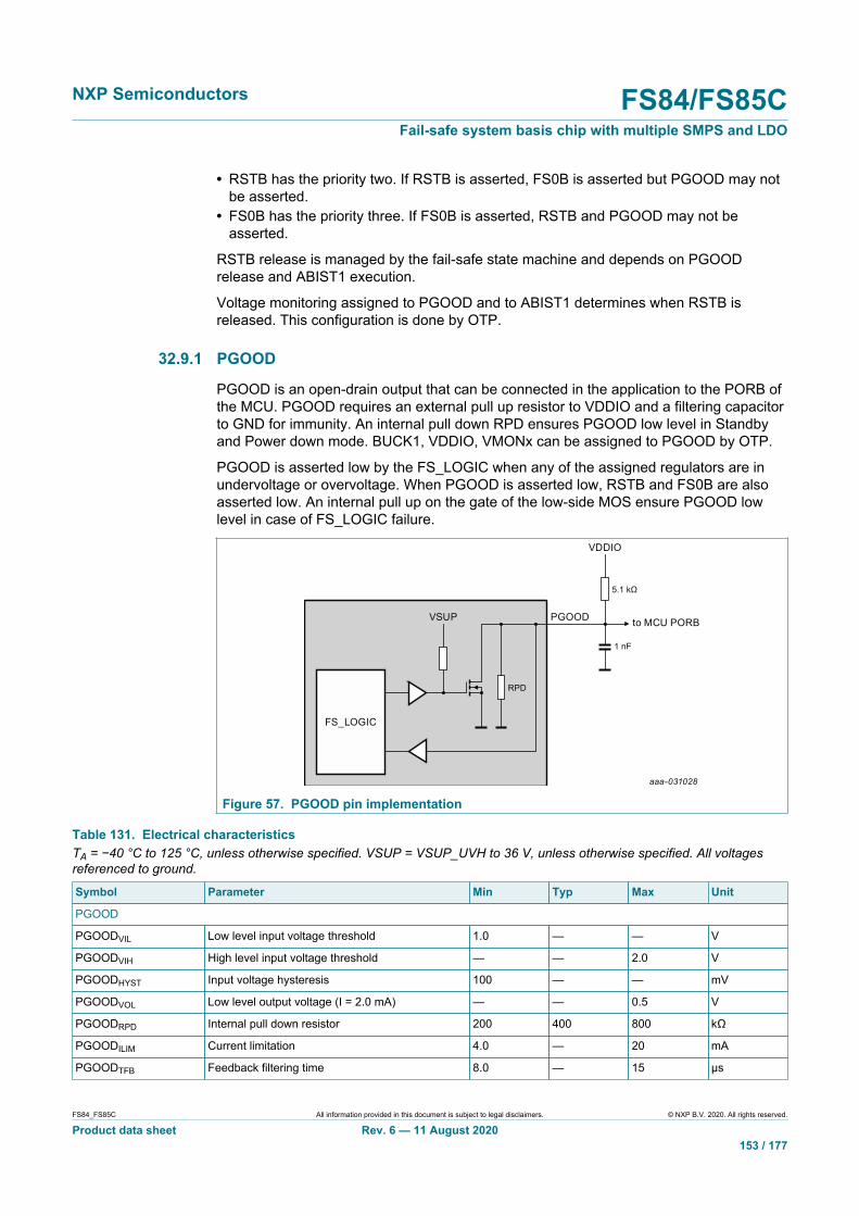
NXP Semiconductors FS84/FS85CFail-safe system basis chip with multiple SMPS and LDO
FS84_FS85C All information provided in this document is subject to legal disclaimers. © NXP B.V. 2020. All rights reserved.
Product data sheet Rev. 6 — 11 August 2020153 / 177
• RSTB has the priority two. If RSTB is asserted, FS0B is asserted but PGOOD may notbe asserted.
• FS0B has the priority three. If FS0B is asserted, RSTB and PGOOD may not beasserted.
RSTB release is managed by the fail-safe state machine and depends on PGOODrelease and ABIST1 execution.
Voltage monitoring assigned to PGOOD and to ABIST1 determines when RSTB isreleased. This configuration is done by OTP.
32.9.1 PGOOD
PGOOD is an open-drain output that can be connected in the application to the PORB ofthe MCU. PGOOD requires an external pull up resistor to VDDIO and a filtering capacitorto GND for immunity. An internal pull down RPD ensures PGOOD low level in Standbyand Power down mode. BUCK1, VDDIO, VMONx can be assigned to PGOOD by OTP.
PGOOD is asserted low by the FS_LOGIC when any of the assigned regulators are inundervoltage or overvoltage. When PGOOD is asserted low, RSTB and FS0B are alsoasserted low. An internal pull up on the gate of the low-side MOS ensure PGOOD lowlevel in case of FS_LOGIC failure.
aaa-031028
FS_LOGIC
VSUP PGOOD to MCU PORB
VDDIO
RPD
5.1 kΩ
1 nF
Figure 57. PGOOD pin implementation
Table 131. Electrical characteristicsTA = −40 °C to 125 °C, unless otherwise specified. VSUP = VSUP_UVH to 36 V, unless otherwise specified. All voltagesreferenced to ground.
Symbol Parameter Min Typ Max Unit
PGOOD
PGOODVIL Low level input voltage threshold 1.0 — — V
PGOODVIH High level input voltage threshold — — 2.0 V
PGOODHYST Input voltage hysteresis 100 — — mV
PGOODVOL Low level output voltage (I = 2.0 mA) — — 0.5 V
PGOODRPD Internal pull down resistor 200 400 800 kΩ
PGOODILIM Current limitation 4.0 — 20 mA
PGOODTFB Feedback filtering time 8.0 — 15 μs

NXP Semiconductors FS84/FS85CFail-safe system basis chip with multiple SMPS and LDO
FS84_FS85C All information provided in this document is subject to legal disclaimers. © NXP B.V. 2020. All rights reserved.
Product data sheet Rev. 6 — 11 August 2020154 / 177
32.9.2 RSTB
RSTB is an open-drain output that can be connected in the application to the RESET ofthe MCU. RSTB requires an external pull up resistor to VDDIO and a filtering capacitorto GND for immunity. An internal pull down RPD ensure RSTB low level in Standby andPower down mode. RSTB assertion depends on the device configuration during INIT_FSphase. When RSTB is asserted low, FS0B is also asserted low. An internal pull up on thegate of the low-side MOS ensures RSTB low level in case of FS_LOGIC failure. WhenRSTB is stuck low for more than RSTBT8S, the device transitions in DEEP-FS mode.
aaa-031029
FS_LOGIC
VSUP RSTB to MCU reset
VDDIO
RPD
5.1 kΩ
1 nF
Figure 58. RSTB pin implementation
Table 132. Electrical characteristicsTA = −40 °C to 125 °C, unless otherwise specified. VSUP = VSUP_UVH to 36 V, unless otherwise specified. All voltagesreferenced to ground.
Symbol Parameter Min Typ Max Unit
RSTB
RSTBVIL Low level input voltage threshold 1.0 — — V
RSTBVIH High level input voltage threshold — — 2.0 V
RSTBHYST Input voltage hysteresis 100 — — mV
RSTBVOL Low level output voltage (I = 2.0 mA) — — 0.5 V
RSTBRPB Internal pull-down resistor 200 400 800 kΩ
RSTBILIM Current limitation 4.0 — 20 mA
RSTBTFB Feedback filtering time 8.0 — 15 μs
RSTBTSC Short to high filtering time 500 — 800 us
RSTBTLG Long pulse (configurable with RSTB_DUR bit) 9.0 — 11 ms
RSTBTST Short pulse (configurable with RSTB_DUR bit) 0.9 — 1.1 ms
RSTBT8S 8 second timer 7.0 8.0 9.0 s
RSTBTRELEASETime to release RSTB from Wake-up or POR withall regulators started in Slot 0 — 8 — ms
32.9.3 FS0B
FS0B is an open-drain output that can be used to transition the system in safe sate.FS0B requires an external pull up resistor to VDDIO or VSUP, a 10 nF filtering capacitor
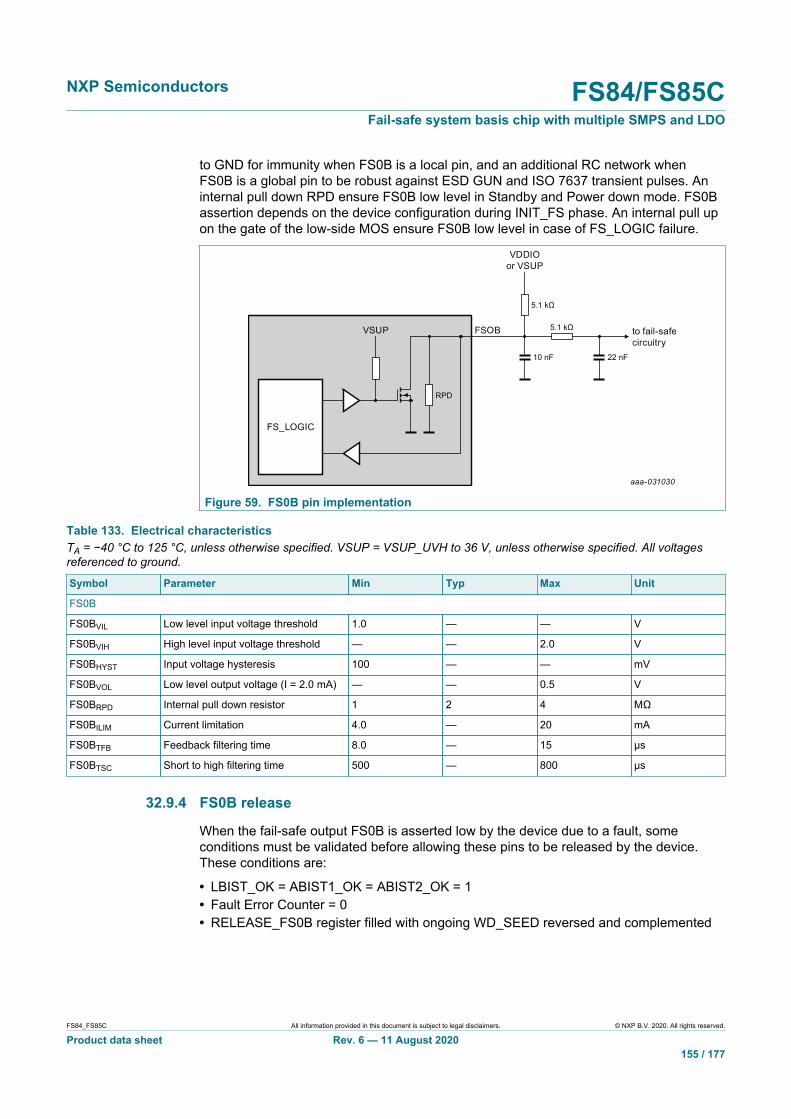
NXP Semiconductors FS84/FS85CFail-safe system basis chip with multiple SMPS and LDO
FS84_FS85C All information provided in this document is subject to legal disclaimers. © NXP B.V. 2020. All rights reserved.
Product data sheet Rev. 6 — 11 August 2020155 / 177
to GND for immunity when FS0B is a local pin, and an additional RC network whenFS0B is a global pin to be robust against ESD GUN and ISO 7637 transient pulses. Aninternal pull down RPD ensure FS0B low level in Standby and Power down mode. FS0Bassertion depends on the device configuration during INIT_FS phase. An internal pull upon the gate of the low-side MOS ensure FS0B low level in case of FS_LOGIC failure.
aaa-031030
FS_LOGIC
VSUP FSOB to fail-safecircuitry
VDDIOor VSUP
RPD
5.1 kΩ
5.1 kΩ
10 nF 22 nF
Figure 59. FS0B pin implementation
Table 133. Electrical characteristicsTA = −40 °C to 125 °C, unless otherwise specified. VSUP = VSUP_UVH to 36 V, unless otherwise specified. All voltagesreferenced to ground.
Symbol Parameter Min Typ Max Unit
FS0B
FS0BVIL Low level input voltage threshold 1.0 — — V
FS0BVIH High level input voltage threshold — — 2.0 V
FS0BHYST Input voltage hysteresis 100 — — mV
FS0BVOL Low level output voltage (I = 2.0 mA) — — 0.5 V
FS0BRPD Internal pull down resistor 1 2 4 MΩ
FS0BILIM Current limitation 4.0 — 20 mA
FS0BTFB Feedback filtering time 8.0 — 15 μs
FS0BTSC Short to high filtering time 500 — 800 μs
32.9.4 FS0B release
When the fail-safe output FS0B is asserted low by the device due to a fault, someconditions must be validated before allowing these pins to be released by the device.These conditions are:
• LBIST_OK = ABIST1_OK = ABIST2_OK = 1• Fault Error Counter = 0• RELEASE_FS0B register filled with ongoing WD_SEED reversed and complemented
NXP Semiconductors FS84/FS85CFail-safe system basis chip with multiple SMPS and LDO
FS84_FS85C All information provided in this document is subject to legal disclaimers. © NXP B.V. 2020. All rights reserved.
Product data sheet Rev. 6 — 11 August 2020156 / 177
Table 134. RELEASE_FS0B register based on WD_SEED valueWD_SEED[23:16] B23 B22 B21 B20 B19 B18 B17 B16
RELEASE_FS0B[23:16] Not(B8) Not(B9) Not(B10) Not(B11) Not(B12) Not(B13) Not(B14) Not(B15)
WD_SEED[15:8] B15 B14 B13 B12 B11 B10 B9 B8
RELEASE_FS0B[15:8] Not(B16) Not(B17) Not(B18) Not(B19) Not(B20) Not(B21) Not(B22) Not(B23)
32.10 Built-in self-test (BIST)
32.10.1 Logical BIST
The fail-safe state machine includes a logical built-in self-test (LBIST) to verify the correctfunctionality of the safety logic monitoring. The LBIST is performed after each POR, orafter each wake up from Standby. In case of LBIST fail, RSTB and PGOOD are releasedbut FS0B remains stuck low and cannot be released. The flag LBIST_OK is availablethrough SPI/I2C for MCU diagnostic. The typical LBIST duration is 4.2 ms and themaximum LBIST duration is 6.0 ms.
32.10.2 Analog BIST
The fail-safe state machine includes two analog built-in self-test (ABIST) to verify thecorrect functionality of the safety analog monitoring. ABIST1 is executed automaticallyafter each POR, or after each wake up from Standby. The assignment of which regulatoris checked during ABIST1 is done by OTP.
ABIST2 is executed after INIT_FS is closed with a good WD refresh and the regulatorsassigned to ABIST2 in FS_I_OVUV_SAFE_REACTION1 register during INIT_FSare started and they crossed their UV. In case of ABIST fail, RSTB and PGOOD arereleased but FS0B remains stuck low and cannot be released. The flags ABIST1_OKand ABIST2_OK are available through SPI/I2C for MCU diagnostic.
Table 135. ABIST coverageParameter Overvoltage Undervoltage Short to high Low speed High speed ABIST1 ABIST2
VCOREMON X X OTP SPI/I2C
VDDIO X X OTP SPI/I2C
VMONx X X OTP SPI/I2C
OSC X X X
V1p6D_FS X X
PGOOD X X
RSTB X X
FS0B X X

NXP Semiconductors FS84/FS85CFail-safe system basis chip with multiple SMPS and LDO
FS84_FS85C All information provided in this document is subject to legal disclaimers. © NXP B.V. 2020. All rights reserved.
Product data sheet Rev. 6 — 11 August 2020157 / 177
Table 136. ABIST2 execution bitVCOREMON_ABIST2 VCOREMON BIST executed during ABIST2
0 (default) No ABIST2
1 VCOREMON BIST executed during ABIST2
Reset condition POR
VDDIO_ABIST2 VDDIO BIST executed during ABIST2
0 (default) No ABIST2
1 VDDIO BIST executed during ABIST2
Reset condition POR
VMONx_ABIST2 VMONx BIST executed during ABIST2
0 (default) No ABIST2
1 VMONx BIST executed during ABIST2
Reset condition POR
Table 137. Electrical characteristicsTA = −40 °C to 125 °C, unless otherwise specified. VSUP = VSUP_UVH to 36 V, unless otherwise specified. All voltagesreferenced to ground.
Symbol Parameter Min Typ Max Unit
ABIST
ABIST1TDUR
ABIST1 duration• MIN with no voltage monitoring assigned by
OTP• MAX with all voltage monitoring assigned by
OTP
0.2 — 1.2 ms
ABIST2TDUR
ABIST2 duration• MIN with no voltage monitoring selected by
SPI/I2C• MAX with all voltage monitoring selected by
SPI/I2C
0.2 — 1.2 ms
33 Package information
FS85/FS84 package is a QFN (sawn), thermally enhanced wettable flanks, 8 x 8 x 0.85mm, 0.5 mm pitch, 56 pins.
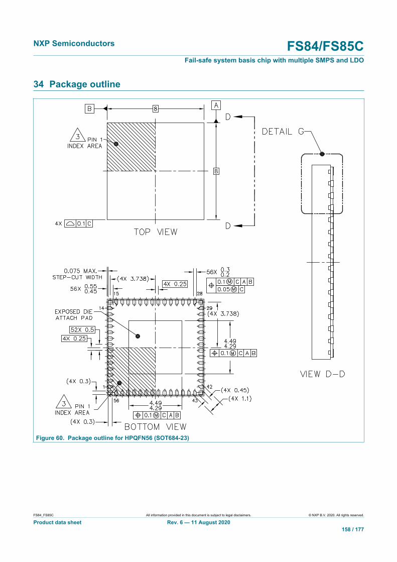
NXP Semiconductors FS84/FS85CFail-safe system basis chip with multiple SMPS and LDO
FS84_FS85C All information provided in this document is subject to legal disclaimers. © NXP B.V. 2020. All rights reserved.
Product data sheet Rev. 6 — 11 August 2020158 / 177
34 Package outline
Figure 60. Package outline for HPQFN56 (SOT684-23)
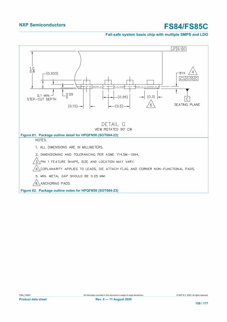
NXP Semiconductors FS84/FS85CFail-safe system basis chip with multiple SMPS and LDO
FS84_FS85C All information provided in this document is subject to legal disclaimers. © NXP B.V. 2020. All rights reserved.
Product data sheet Rev. 6 — 11 August 2020159 / 177
Figure 61. Package outline detail for HPQFN56 (SOT684-23)
Figure 62. Package outline notes for HPQFN56 (SOT684-23)

NXP Semiconductors FS84/FS85CFail-safe system basis chip with multiple SMPS and LDO
FS84_FS85C All information provided in this document is subject to legal disclaimers. © NXP B.V. 2020. All rights reserved.
Product data sheet Rev. 6 — 11 August 2020160 / 177
35 Layout and PCB guidelines
35.1 Landing pad information
Figure 63. Solder mask pattern
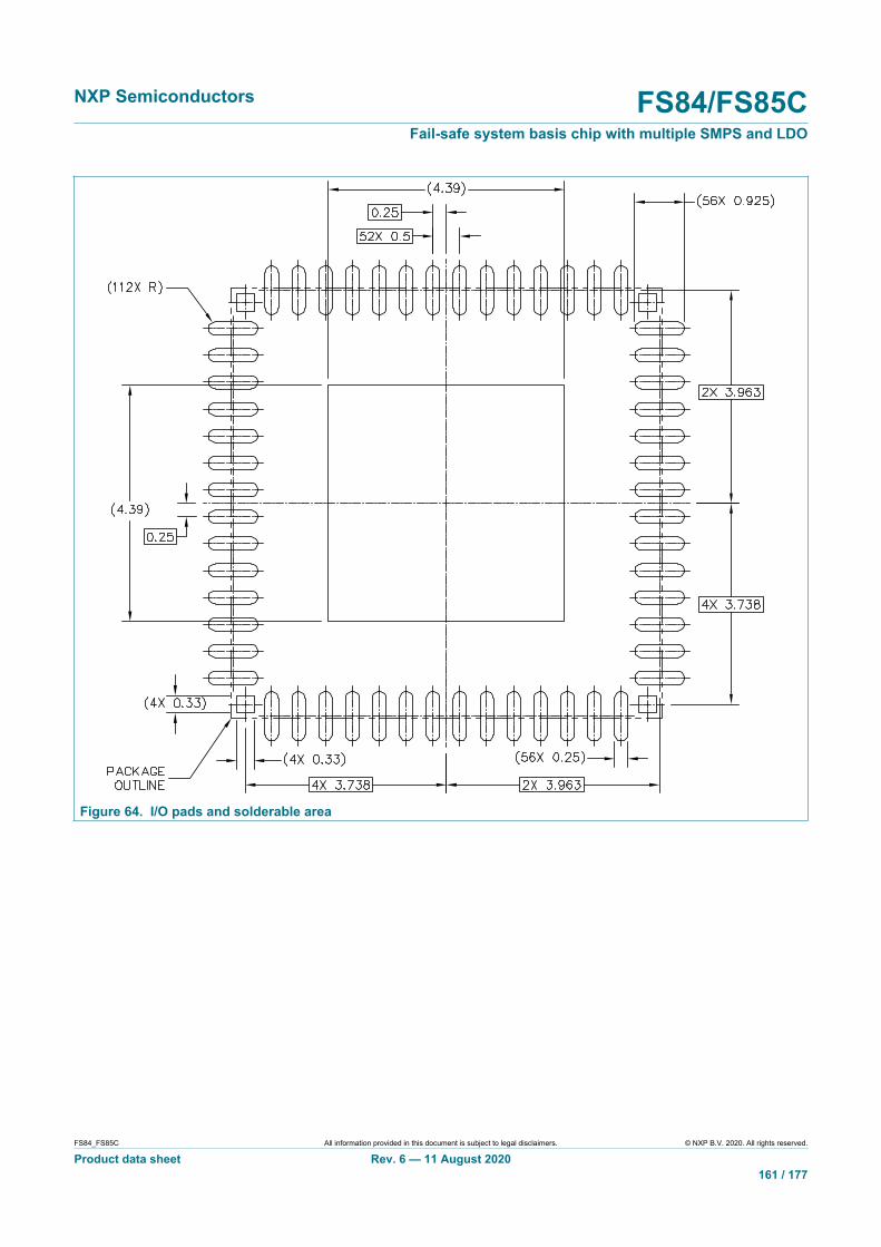
NXP Semiconductors FS84/FS85CFail-safe system basis chip with multiple SMPS and LDO
FS84_FS85C All information provided in this document is subject to legal disclaimers. © NXP B.V. 2020. All rights reserved.
Product data sheet Rev. 6 — 11 August 2020161 / 177
Figure 64. I/O pads and solderable area
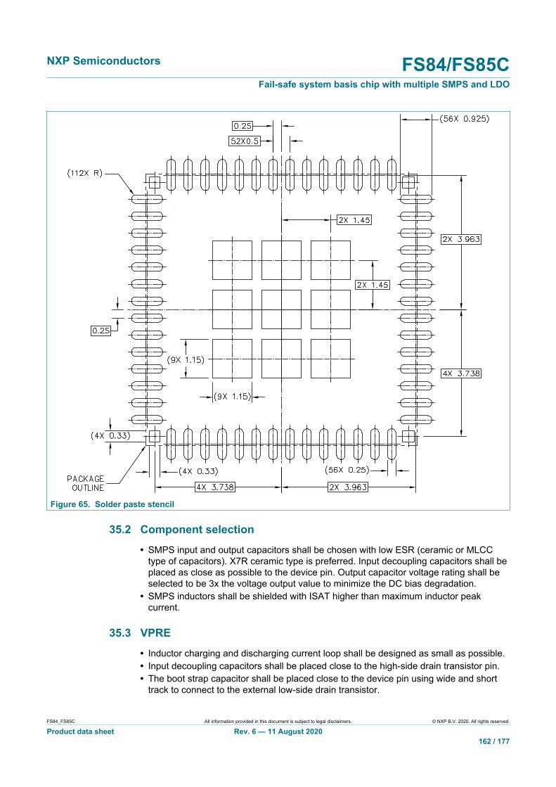
NXP Semiconductors FS84/FS85CFail-safe system basis chip with multiple SMPS and LDO
FS84_FS85C All information provided in this document is subject to legal disclaimers. © NXP B.V. 2020. All rights reserved.
Product data sheet Rev. 6 — 11 August 2020162 / 177
Figure 65. Solder paste stencil
35.2 Component selection• SMPS input and output capacitors shall be chosen with low ESR (ceramic or MLCC
type of capacitors). X7R ceramic type is preferred. Input decoupling capacitors shall beplaced as close as possible to the device pin. Output capacitor voltage rating shall beselected to be 3x the voltage output value to minimize the DC bias degradation.
• SMPS inductors shall be shielded with ISAT higher than maximum inductor peakcurrent.
35.3 VPRE• Inductor charging and discharging current loop shall be designed as small as possible.• Input decoupling capacitors shall be placed close to the high-side drain transistor pin.• The boot strap capacitor shall be placed close to the device pin using wide and short
track to connect to the external low-side drain transistor.

NXP Semiconductors FS84/FS85CFail-safe system basis chip with multiple SMPS and LDO
FS84_FS85C All information provided in this document is subject to legal disclaimers. © NXP B.V. 2020. All rights reserved.
Product data sheet Rev. 6 — 11 August 2020163 / 177
• PRE_GLS, PRE_GHS and PRE_SW tracks shall be wide and short and should notcross any sensitive signal (current sensing, for example).
aaa-031036
L1 connection
ImplementationNote: L2 is system ground.
FS85L3 connection
1 2 3 4PR
E_G
HS
PRE_
SWPR
E_G
LS
• PRE_FB used as voltage feedback AND current sense shall be connected to RSHUNT
and routed as a pair with CSP.
aaa-035666
layout as a pairdo not cross any noisy signal
FS85
GND
coil cap
ground plane
Rshunt
GND
CSP
PRE_
FB
• The external transistor thermal shape should be in the range of 25 x 25 mm for
optimum Rth.• See LFPAK56 application note for more details: http://assets.nexperia.com/documents/
application-note/AN10874.pdf
35.4 VBUCKx• Inductor charging and discharging current loop shall be designed as small as possible.
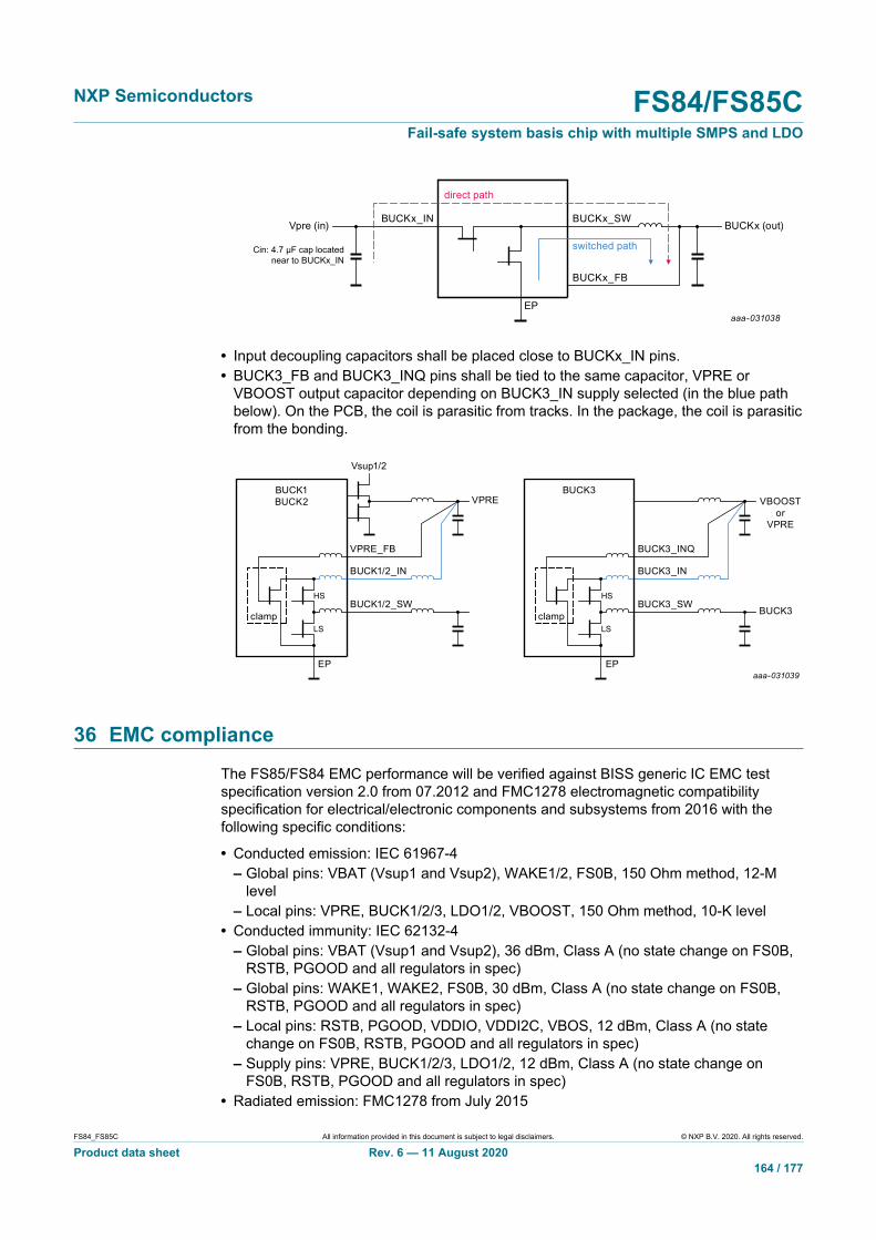
NXP Semiconductors FS84/FS85CFail-safe system basis chip with multiple SMPS and LDO
FS84_FS85C All information provided in this document is subject to legal disclaimers. © NXP B.V. 2020. All rights reserved.
Product data sheet Rev. 6 — 11 August 2020164 / 177
aaa-031038
BUCKx_IN BUCKx_SW
EP
switched path
direct path
Vpre (in) BUCKx (out)
Cin: 4.7 µF cap locatednear to BUCKx_IN
BUCKx_FB
• Input decoupling capacitors shall be placed close to BUCKx_IN pins.• BUCK3_FB and BUCK3_INQ pins shall be tied to the same capacitor, VPRE or
VBOOST output capacitor depending on BUCK3_IN supply selected (in the blue pathbelow). On the PCB, the coil is parasitic from tracks. In the package, the coil is parasiticfrom the bonding.
aaa-031039
BUCK1BUCK2
VPRE_FB
Vsup1/2
VPRE
BUCK1/2_IN
BUCK1/2_SW
EP
clamp
HS
LS
BUCK3
BUCK3_INQ
VBOOSTor
VPRE
BUCK3
BUCK3_IN
BUCK3_SW
EP
clamp
HS
LS
36 EMC compliance
The FS85/FS84 EMC performance will be verified against BISS generic IC EMC testspecification version 2.0 from 07.2012 and FMC1278 electromagnetic compatibilityspecification for electrical/electronic components and subsystems from 2016 with thefollowing specific conditions:
• Conducted emission: IEC 61967-4– Global pins: VBAT (Vsup1 and Vsup2), WAKE1/2, FS0B, 150 Ohm method, 12-M
level– Local pins: VPRE, BUCK1/2/3, LDO1/2, VBOOST, 150 Ohm method, 10-K level
• Conducted immunity: IEC 62132-4– Global pins: VBAT (Vsup1 and Vsup2), 36 dBm, Class A (no state change on FS0B,
RSTB, PGOOD and all regulators in spec)– Global pins: WAKE1, WAKE2, FS0B, 30 dBm, Class A (no state change on FS0B,
RSTB, PGOOD and all regulators in spec)– Local pins: RSTB, PGOOD, VDDIO, VDDI2C, VBOS, 12 dBm, Class A (no state
change on FS0B, RSTB, PGOOD and all regulators in spec)– Supply pins: VPRE, BUCK1/2/3, LDO1/2, 12 dBm, Class A (no state change on
FS0B, RSTB, PGOOD and all regulators in spec)• Radiated emission: FMC1278 from July 2015
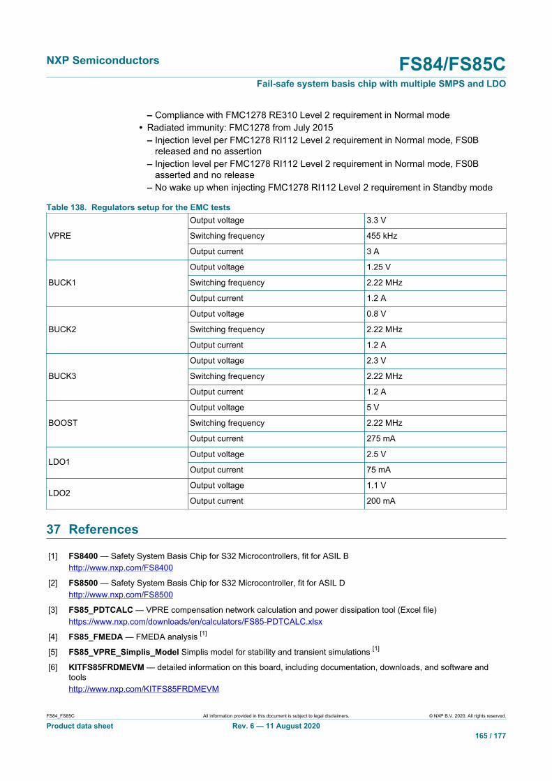
NXP Semiconductors FS84/FS85CFail-safe system basis chip with multiple SMPS and LDO
FS84_FS85C All information provided in this document is subject to legal disclaimers. © NXP B.V. 2020. All rights reserved.
Product data sheet Rev. 6 — 11 August 2020165 / 177
– Compliance with FMC1278 RE310 Level 2 requirement in Normal mode• Radiated immunity: FMC1278 from July 2015
– Injection level per FMC1278 RI112 Level 2 requirement in Normal mode, FS0Breleased and no assertion
– Injection level per FMC1278 RI112 Level 2 requirement in Normal mode, FS0Basserted and no release
– No wake up when injecting FMC1278 RI112 Level 2 requirement in Standby mode
Table 138. Regulators setup for the EMC testsOutput voltage 3.3 V
Switching frequency 455 kHzVPRE
Output current 3 A
Output voltage 1.25 V
Switching frequency 2.22 MHzBUCK1
Output current 1.2 A
Output voltage 0.8 V
Switching frequency 2.22 MHzBUCK2
Output current 1.2 A
Output voltage 2.3 V
Switching frequency 2.22 MHzBUCK3
Output current 1.2 A
Output voltage 5 V
Switching frequency 2.22 MHzBOOST
Output current 275 mA
Output voltage 2.5 VLDO1
Output current 75 mA
Output voltage 1.1 VLDO2
Output current 200 mA
37 References
[1] FS8400 — Safety System Basis Chip for S32 Microcontrollers, fit for ASIL Bhttp://www.nxp.com/FS8400
[2] FS8500 — Safety System Basis Chip for S32 Microcontroller, fit for ASIL Dhttp://www.nxp.com/FS8500
[3] FS85_PDTCALC — VPRE compensation network calculation and power dissipation tool (Excel file)https://www.nxp.com/downloads/en/calculators/FS85-PDTCALC.xlsx
[4] FS85_FMEDA — FMEDA analysis [1]
[5] FS85_VPRE_Simplis_Model Simplis model for stability and transient simulations [1]
[6] KITFS85FRDMEVM — detailed information on this board, including documentation, downloads, and software andtoolshttp://www.nxp.com/KITFS85FRDMEVM

NXP Semiconductors FS84/FS85CFail-safe system basis chip with multiple SMPS and LDO
FS84_FS85C All information provided in this document is subject to legal disclaimers. © NXP B.V. 2020. All rights reserved.
Product data sheet Rev. 6 — 11 August 2020166 / 177
[7] KITFS85SKTEVM — detailed information on this board, including documentation, downloads, and software and toolshttp://www.nxp.com/KITFS85SKTEVM
[8] KITFS85AEEVM — detailed information on this board, including documentation, downloads, and software and toolshttp://www.nxp.com/KITFS85AEEVM
[9] AN12333 — FS84, FS85 product guidelines application notehttps://www.nxp.com/webapp/sps/download/mod_download.jsp?colCode=AN12333
[10] FS85_FS84_OTP_Config.xlsm — OTP configuration filehttps://www.nxp.com/webapp/Download?colCode=FS85-FS84-OTP
[11] FS85_FS84SMUGC — Safety manual [1]
[1] Contact NXP sales representative.

NXP Semiconductors FS84/FS85CFail-safe system basis chip with multiple SMPS and LDO
FS84_FS85C All information provided in this document is subject to legal disclaimers. © NXP B.V. 2020. All rights reserved.
Product data sheet Rev. 6 — 11 August 2020167 / 177
38 Revision historyTable 139. Revision historyDocument ID Release date Data sheet status Change notice Supersedes
FS84_FS85C v.6.0 20200811 Product data sheet 202007042I FS84_FS85C v.5.0
Modifications • Table 2: added new part numbers (MC33FS8500A0ES, MC33FS8510A0ES, MC33FS8520A0ES,MC33FS8400G0ES, MC33FS8405G0ES, MC33FS8410G0ES, MC33FS8415G0ES, MC33FS8420G0ES,MC33FS8425G0ES, MC33FS8435G0ES)
• Section 4.1: updated OTP configurations for MC33FS8530A4ES, MC33FS8430G2ES, MC33FS8410G3ES,and MC33FS8400G5ES– VBOOST - slope compensation (MC33FS8530A4ES): replaced 160 mV/µs by 125 mV/µs– BUCK2 - output voltage (MC33FS8530A4ES): replaced 1.2 V by 1.8 V– LDO2 - output voltage (MC33FS8530A4ES): replaced 5.0 V by 1.2 V– LDO2 - power sequencing slot (MC33FS8530A4ES): replaced "Regulator does not Start (Enabled by
SPI)" by "Regulator Start and Stop in slot 1"– VBOOST - slope compensation (MC33FS8430G2ES): replaced 140 mV/µs by 160 mV/μs– VPRE - switching frequency (MC33FS8410G3ES): replaced delay 0 by delay 3– LDO1 - current limitation (MC33FS8400G5ES): replaced 150 mA by 400 mA
• Section 4.2: updated OTP configurations for MC33FS8530A4ES– VCOREMON, VDDIOMON, VMON1, VMON2, VMON3, VMON4 - OV_DGLT: replaced 45 µs by 25 µs– VCOREMON, VDDIOMON, VMON1, VMON2, VMON3, VMON4 - UV_DGLT: replaced 40 µs by 5 µs– PGOOD - RSTB: replaced "Yes" by "No"– Watchdog: replaced Challenger WD by Simple WD
• Table 5: added new row under PRE_SW for Transient voltage < 20 ns• Table 28: Updated description for VBOSUVH and VBOOSTUVH (deleted "falling")• Table 130: added footnote "By cascaded effect, the FSOB is asserted low because of INIT_FS state"• Section 32.8.2: updated first paragraph (added "The fault error counter is incremented by 1, each time the
RSTB and/or FS0B pin is asserted")
FS84_FS85C v.5.0 20200129 Product data sheet 201912015I FS84_FS85C v.4.0
Modifications • Section 4, Table 2, revised "MC33FS8030G5ES" to "MC33FS8400G5ES".• Section 22.5, Table 83, revised as follows:
– Revised the parameter description for VBUCK12 to include "0.975 V".– Moved "2.5" from "Max" value to "Typ" value for IBUCK12.– Revised ILIM_BUCK12 parameter description and added new row with new min, typ, and max values.
Revised "VBUCK12_SOFT_START" to "TBUCK12_SOFT_START".• Section 23.4, Table 84, revised as follows:
– Revised "IBUCK12" to "IBUCK3".– Revised the first parameter description for TBUCK3_SOFT_START from "VBUCK12_SOFT_START = VBUCK12 /
VBUCK12_DVS_UP Soft start for VBUCK3 = 1.8 V and OTP_DVS_BUCK3[1:0] = 00" to "VBUCK3_SOFT_START= VBUCK3 / VBUCK3_DVS_UP_DOWN Soft start for VBUCK3 = 1.1 V and OTP_DVS_BUCK3[1:0] = 00"
– Revised the second parameter description for TBUCK3_SOFT_START from "Soft start for VBUCK3 = 1.8 V andOTP_DVS_BUCK3[1:0] = 11 To be recalculated for different VBUCK3 and different VBUCK3_DVS_UP_DOWN"to "Soft start for VBUCK3 = 1.1 V and OTP_DVS_BUCK3[1:0] = 11 To be recalculated for different VBUCK3and different VBUCK3_DVS_UP_DOWN"
NXP Semiconductors FS84/FS85CFail-safe system basis chip with multiple SMPS and LDO
FS84_FS85C All information provided in this document is subject to legal disclaimers. © NXP B.V. 2020. All rights reserved.
Product data sheet Rev. 6 — 11 August 2020168 / 177
Document ID Release date Data sheet status Change notice Supersedes
FS84_FS85C v.4.0 20191205 Product data sheet 201912015I FS84_FS85 v.3.0
Modifications • changed "VBOOST_SW" to "FBOOST_SW" throughout document• Section 4,
– Table 2: removed part number PC33FS8510A3ES; added part number MC33FS8510D3ES; updatedorderable part numbers — replaced "PC" with "MC"
– Table 1: removed part number PC33FS8510A3ES; added part number MC33FS8510D3ES; updatedorderable part numbers — replaced "PC" with "MC"
• Section 4.1: removed VPRE low-side slew rate row; removed part number PC33FS8510A3ES; added partnumber MC33FS8510D3ES; updated orderable part numbers — replaced "PC" with "MC"
• Section 4.2: column heading changed from MC33FS8510A 3ES to MC33FS8510D 3ES• Section 5: updated radar and vision applications• Section 7.2, Table 3: updated EP description• Section 9, Table 5
– "All other pins", Min changed from –1.0 to –0.3– Added BUCKx_SW | Transient voltage<20ns | BUCK1_SW, BUCK2_SW, BUCK3_SW | -3.0 | 6.5 | V |
• Section 10: updated ESD Charged device model• Section 11: updated content starting with paragraph "When VPRE is switching..."• Section 12, Table 6
– changed TA parameter from "Ambient temperature" to "Ambient temperature (Grade 1)"– changed TJ parameter from "Junction temperature" to "Junction temperature (Grade 1)"
• Section 14.1: updated Figure 5• Section 14.2, final paragraph: replaced "WAKE1 or WAKE2 > WAKE12VIH" with "WAKE1 > WAKE12VIH"• Section 14.3, updated first and second paragraph• Section 14.4: updated first and second paragraphs• Section 14.5
– added paragraph "Refer to AN12333 for more details on Debug mode entry implementation."– Table 8: updated TDBG
• Section 15: updated FS_WD_ANSWER register• Section 16.1
– M_MODE register, changed field name "GOTOSTBY" to "GoToSTBY"– M_MEMORYx registers, changed field names "M_MEMORYx" to "MEMORYx"
• Section 16.2– M_MEMORYx registers, changed field names "M_MEMORYx" to "MEMORYx"– updated M_DEVICEID register
• Section 16.4: changed field name "GOTOSTBY" to "GoToSTBY"; changed GoToSTBY reset condition from"n.a." to "POR"
NXP Semiconductors FS84/FS85CFail-safe system basis chip with multiple SMPS and LDO
FS84_FS85C All information provided in this document is subject to legal disclaimers. © NXP B.V. 2020. All rights reserved.
Product data sheet Rev. 6 — 11 August 2020169 / 177
Document ID Release date Data sheet status Change notice Supersedes
• Section 16.6: changed VPRESRLS[1:0] bit reset values from "OTP" to "1"• Section 16.7: updated RATIO field value = 0 description and value =1 description• Section 16.11: changed VBOSUVH field reset value from "0" to "1"; changed VBOOSTUVH field reset value
from "1" to "0"• Section 16.15: changed field names "M_MEMORY0" to "MEMORY0"• Section 16.16: changed field names "M_MEMORY1" to "MEMORY1"; changed bits 23 to 16 field name
from MEMORY1[15:0] to MEMORY1[15:8]; changed bits 15 to 8 field name from MEMORY1[15:0] toMEMORY1[7:0]
• Section 16.17: updated fields and descriptions• Section 17.15: changed PGOOD_EVENT reset value from "0" to "1"; changed RSTB_EVENT reset value
from "0" to "1"• Section 18.1, Table 75: changed OTP_CFG_BOOST_1 bit 5 to "VPRE_MODE"; changed
OTP_CFG_SEQ_3 bit[7:6] to DVS_BUCK12[1:0], bit[5:4] to DVS_BUCK3[1:0], bit[3] to Tslot• Section 18.2, Table 76: added descriptions for OTP_CFG_BOOST_1; updated OTP_CFG_SEQ_3 register;
updated OTP_CFG_SM_2 register PSYNC_CFG field description• Section 18.4: OTP_CFG_UVOV_3 register: changed "(12.5mV)" to "(-12.5 mV)"; changed "(25mV)" to "(-25
mV)"; changed "(50mV)" to "(-50 mV)"; changed "(100mV)" to "(-100 mV)"• Section 19.2: updated COUT_BOS• Section 20.1: updated first and second paragraph• Section 20.3: updated content with changes to the calculation guideline• Section 20.4
– updated VPRE_SOFT_START, FPRE_SW, LVPRE, VPRE_LOAD_REG_455k, VPRE_LIM_TH1, ILIM_PRE, IPRE_GATE_DRV,COUT_PRE, CIN_PRE, IPRE_DRV, gmEAPRE, TPRE_DT
– added VPRE_LINE_REG_455k, VPRE_LINE_REG_2.2M, VPRE_LOAD_REG_2.2M, VPRE_RIPPLE_455k, VPRE_RIPPLE_2.2M• Section 20.5: updated content• Section 20.6; updated Figure 16• Section 21.4: updated COUT_BOOST, ILIM_BOOST, TBOOST_ON_MIN, gmEABOOST, RCOMP• Section 22.1: updated final paragraph• Section 22.5: updated VBUCK12, IBUCK12, COUT_BUCK12, CIN_BUCK12, VBUCK12_TLR, VBUCK12_TLR,
VBUCK12_TLR, ILIM_BUCK12, VBUCK12_DVS_UP (for VBUCK12 up to 1.5V), VBUCK12_DVS_UP_1p8 (for VBUCK12= 1.8V), VBUCK12_DVS_DOWN(for VBUCK12 up to 1.5V), VBUCK12_DVS_DOWN_1p8 (for VBUCK12 = 1.8V),VBUCK12_SOFT_START, TBUCK12_DT
• Section 22.6: updated Figure 24• Section 23.1: updated paragraph starting "BUCK3 is part number dependent..."• Section 23.4: updated COUT_BUCK3, CIN_BUCK3; added VBUCK3_DVS_UP_DOWN, TBUCK3_SOFT_START, TBUCK3_DT• Section 23.5: updated Figure 28• Section 25.1, third paragraph: changed "VPRE switching frequency is coming from CLK2 (455 kHz)" to
"VPRE switching frequency is coming from CLK2 (455 kHz) or CLK1 (2.22 MHz)"• Section 25.4, second paragraph: changed "It is recommended to select 23 kHz carrier frequency when
VPRE is configured at 455 kHz." to "It is recommended to select 23 kHz carrier frequency when VPRE isconfigured at 455 kHz and 94 kHz when VPRE is configured at 2.2 MHz for the best performance."
• Section 25.5: first paragraph: removed "If FIN is out of range, CLK clock moves back to internal oscillatorand report the error using the CLK_FIN_DIV_OK bit."; added paragraph starting "If FIN is out of range,"
• Section 25.6: updated FINRANGE• Section 26.3: updated 00100 row: changed "T(°C) = (VAMUX – VTEMP25) / VTEMP_COEFF + 25" to T(°C) =
[(VAMUX – VTEMP25) / VTEMP_COEFF] + 25• Section 27.1: paragraph starting "WAKE1 and WAKE2 are level based": changed "WAKE1 can be for
example connected to VBAT " to "WAKE1 can be for example connected to a switched VBAT (KL15 line) ",changed "When a WAKE pin is used as a global pin, a CRC protection" to "When a WAKE pin is used as aglobal pin, a C - R - C protection" ; Table 91: undated IWAKE12
• Section 27.2 Table 93: removed VPRE_UVL and BOOST_OC• Section 27.4: updated paragraphs and figure titles to reference external PMIC instead of PF82; changed
"VSNS pin of PF82" to "VSNVS pin of PF82"• Section 28: first paragraph: changed "An 8 bit CRC is required for each Write and Read SPI command."
to "An 8 bit CRC is required for each Write and Read SPI and I2C command. "; updated second and thirdparagraphs for clarity; updated Figure 40; changed Table 96 title from "Data preparation for CRC encoding"to "Data preparation for CRC encoding (SPI format)"
• Section 29.1, updated paragraph starting with "the MCU is the master driving …"

NXP Semiconductors FS84/FS85CFail-safe system basis chip with multiple SMPS and LDO
FS84_FS85C All information provided in this document is subject to legal disclaimers. © NXP B.V. 2020. All rights reserved.
Product data sheet Rev. 6 — 11 August 2020170 / 177
Document ID Release date Data sheet status Change notice Supersedes
• Section 29.2: changed topic title from "SPI CRC calculation" to "SPI CRC calculation and results"; addedtitle to Table 98; added Table 99
• Section 29.3 Table 100: removed tCBS_MIN• Updated Section 30.3• Replaced section titled "29.3 Cyclic redundant check" with Section 30.3 "I2C CRC calculation and results"• Section 31: updated Figure 42• Section 32.3: added paragraph starting with "After INIT_FS closure, …."• Section 32.8.2: updated final paragraph starting with "If OTP_GOOD_RSTB = '1', …."• Section 32.10.2: updated second paragraph starting with "ABIST2 is executed after INIT_FS.…"• Updated Section 35.3• Updated Section 35.4• Section 37: updated reference [11]: changed "FS84_FS84SMUG" to "FS84_FS84SMUGC", removed
reference [12] ES_FS84_FS85—Errata sheet• Section 32.5.3: updated FCCU12RATIO
FS84_FS85 v.3.0 20190409 Product data sheet - FS84_FS85 v.2.0
Modifications • Section 10.2: updated description• Section 15: renamed column R/W to R/W SPI and added a column R/W I2C
FS84_FS85 v.2.0 20190315 Product data sheet - FS84_FS85 v.1.0
Modifications • Section 4: added part numbers and corresponding OTP flavors• Section 11: updated Figure 4, assumptions and description• Global: corrected minor typos• Table 67: replaced FCCU1_RT by FCCU2_RT for bit 9 and FCCU2_RT by FCCU1_RT for bit 8• Section 34 and Section 35: updated case outline• Table 5: added parameters for BUCKx_IN• Table 76: replaced CLK_DIV1 by 2.22 MHz• Table 76: updated the value and description for OTP_CFG_CLOCK_4 register bit 3 (replaced 0 by 1 and
2.22 MHz by 455 kHz)• Section 20.1: replaced "VSUP = VPRE / (TPRE_ON_MIN × FPRE_SW)" by "VSUP = LPI_DCR × IPRE + VPRE_UVL /
DMAX with DMAX = 1 − (FPRE_SW × TPRE_OFF_MIN)"• Figure 16: deleted 2.22 MHz curves
FS84_FS85 v.1.0 20190122 Preliminary data sheet - -

NXP Semiconductors FS84/FS85CFail-safe system basis chip with multiple SMPS and LDO
FS84_FS85C All information provided in this document is subject to legal disclaimers. © NXP B.V. 2020. All rights reserved.
Product data sheet Rev. 6 — 11 August 2020171 / 177
39 Legal information
39.1 Data sheet status
Document status[1][2] Product status[3] Definition
Objective [short] data sheet Development This document contains data from the objective specification for productdevelopment.
Preliminary [short] data sheet Qualification This document contains data from the preliminary specification.
Product [short] data sheet Production This document contains the product specification.
[1] Please consult the most recently issued document before initiating or completing a design.[2] The term 'short data sheet' is explained in section "Definitions".[3] The product status of device(s) described in this document may have changed since this document was published and may differ in case of multiple
devices. The latest product status information is available on the Internet at URL http://www.nxp.com.
39.2 DefinitionsDraft — The document is a draft version only. The content is still underinternal review and subject to formal approval, which may result inmodifications or additions. NXP Semiconductors does not give anyrepresentations or warranties as to the accuracy or completeness ofinformation included herein and shall have no liability for the consequencesof use of such information.
Short data sheet — A short data sheet is an extract from a full data sheetwith the same product type number(s) and title. A short data sheet isintended for quick reference only and should not be relied upon to containdetailed and full information. For detailed and full information see therelevant full data sheet, which is available on request via the local NXPSemiconductors sales office. In case of any inconsistency or conflict with theshort data sheet, the full data sheet shall prevail.
Product specification — The information and data provided in a Productdata sheet shall define the specification of the product as agreed betweenNXP Semiconductors and its customer, unless NXP Semiconductors andcustomer have explicitly agreed otherwise in writing. In no event however,shall an agreement be valid in which the NXP Semiconductors productis deemed to offer functions and qualities beyond those described in theProduct data sheet.
39.3 DisclaimersLimited warranty and liability — Information in this document is believedto be accurate and reliable. However, NXP Semiconductors does notgive any representations or warranties, expressed or implied, as to theaccuracy or completeness of such information and shall have no liabilityfor the consequences of use of such information. NXP Semiconductorstakes no responsibility for the content in this document if provided by aninformation source outside of NXP Semiconductors. In no event shall NXPSemiconductors be liable for any indirect, incidental, punitive, special orconsequential damages (including - without limitation - lost profits, lostsavings, business interruption, costs related to the removal or replacementof any products or rework charges) whether or not such damages are basedon tort (including negligence), warranty, breach of contract or any otherlegal theory. Notwithstanding any damages that customer might incur forany reason whatsoever, NXP Semiconductors’ aggregate and cumulativeliability towards customer for the products described herein shall be limitedin accordance with the Terms and conditions of commercial sale of NXPSemiconductors.
Right to make changes — NXP Semiconductors reserves the right tomake changes to information published in this document, including withoutlimitation specifications and product descriptions, at any time and without
notice. This document supersedes and replaces all information supplied priorto the publication hereof.
Applications — Applications that are described herein for any of theseproducts are for illustrative purposes only. NXP Semiconductors makesno representation or warranty that such applications will be suitablefor the specified use without further testing or modification. Customersare responsible for the design and operation of their applications andproducts using NXP Semiconductors products, and NXP Semiconductorsaccepts no liability for any assistance with applications or customer productdesign. It is customer’s sole responsibility to determine whether the NXPSemiconductors product is suitable and fit for the customer’s applicationsand products planned, as well as for the planned application and use ofcustomer’s third party customer(s). Customers should provide appropriatedesign and operating safeguards to minimize the risks associated withtheir applications and products. NXP Semiconductors does not accept anyliability related to any default, damage, costs or problem which is basedon any weakness or default in the customer’s applications or products, orthe application or use by customer’s third party customer(s). Customer isresponsible for doing all necessary testing for the customer’s applicationsand products using NXP Semiconductors products in order to avoid adefault of the applications and the products or of the application or use bycustomer’s third party customer(s). NXP does not accept any liability in thisrespect.
Limiting values — Stress above one or more limiting values (as defined inthe Absolute Maximum Ratings System of IEC 60134) will cause permanentdamage to the device. Limiting values are stress ratings only and (proper)operation of the device at these or any other conditions above thosegiven in the Recommended operating conditions section (if present) or theCharacteristics sections of this document is not warranted. Constant orrepeated exposure to limiting values will permanently and irreversibly affectthe quality and reliability of the device.
Terms and conditions of commercial sale — NXP Semiconductorsproducts are sold subject to the general terms and conditions of commercialsale, as published at http://www.nxp.com/profile/terms, unless otherwiseagreed in a valid written individual agreement. In case an individualagreement is concluded only the terms and conditions of the respectiveagreement shall apply. NXP Semiconductors hereby expressly objects toapplying the customer’s general terms and conditions with regard to thepurchase of NXP Semiconductors products by customer.
No offer to sell or license — Nothing in this document may be interpretedor construed as an offer to sell products that is open for acceptance orthe grant, conveyance or implication of any license under any copyrights,patents or other industrial or intellectual property rights.
Suitability for use in automotive applications — This NXPSemiconductors product has been qualified for use in automotiveapplications. Unless otherwise agreed in writing, the product is not designed,authorized or warranted to be suitable for use in life support, life-critical orsafety-critical systems or equipment, nor in applications where failure ormalfunction of an NXP Semiconductors product can reasonably be expected

NXP Semiconductors FS84/FS85CFail-safe system basis chip with multiple SMPS and LDO
FS84_FS85C All information provided in this document is subject to legal disclaimers. © NXP B.V. 2020. All rights reserved.
Product data sheet Rev. 6 — 11 August 2020172 / 177
to result in personal injury, death or severe property or environmentaldamage. NXP Semiconductors and its suppliers accept no liability forinclusion and/or use of NXP Semiconductors products in such equipment orapplications and therefore such inclusion and/or use is at the customer's ownrisk.
Export control — This document as well as the item(s) described hereinmay be subject to export control regulations. Export might require a priorauthorization from competent authorities.
Translations — A non-English (translated) version of a document is forreference only. The English version shall prevail in case of any discrepancybetween the translated and English versions.
39.4 TrademarksNotice: All referenced brands, product names, service names andtrademarks are the property of their respective owners.
NXP — is a trademark of NXP B.V.SafeAssure — is a trademark of NXP B.V.

NXP Semiconductors FS84/FS85CFail-safe system basis chip with multiple SMPS and LDO
FS84_FS85C All information provided in this document is subject to legal disclaimers. © NXP B.V. 2020. All rights reserved.
Product data sheet Rev. 6 — 11 August 2020173 / 177
TablesTab. 1. Device options ...................................................3Tab. 2. Ordering information ..........................................3Tab. 3. Pin description ...................................................9Tab. 4. Connection of unused pins ............................. 11Tab. 5. Maximum ratings .............................................13Tab. 6. Thermal ratings ............................................... 14Tab. 7. Electrical characteristics ..................................15Tab. 8. Electrical characteristics ..................................21Tab. 9. Main writing registers overview ....................... 25Tab. 10. Main reading registers overview ......................26Tab. 11. M_FLAG register bit allocation ........................26Tab. 12. M_FLAG register bit description ......................27Tab. 13. M_MODE register bit allocation ...................... 28Tab. 14. M_MODE register bit description .................... 29Tab. 15. M_REG_CTRL1 register bit allocation ............ 30Tab. 16. M_REG_CTRL1 register bit description .......... 30Tab. 17. M_REG_CTRL2 register bit allocation ............ 32Tab. 18. M_REG_CTRL2 register bit description .......... 32Tab. 19. M_AMUX register bit allocation .......................33Tab. 20. M_AMUX register bit description .....................33Tab. 21. M_CLOCK register bit allocation .....................34Tab. 22. M_CLOCK register bit description ...................34Tab. 23. M_INT_MASK1 register bit allocation ..............35Tab. 24. M_INT_MASK1 register bit description ........... 35Tab. 25. M_INT_MASK2 register bit allocation ..............37Tab. 26. M_INT_MASK2 register bit description ........... 37Tab. 27. M_FLAG1 register bit allocation ......................38Tab. 28. M_FLAG1 register bit description ....................39Tab. 29. M_FLAG2 register bit allocation ......................40Tab. 30. M_FLAG2 register bit description ....................41Tab. 31. M_VMON_REGx register bit allocation ........... 42Tab. 32. M_VMON_REGx register bit description ......... 43Tab. 33. M_LVB1_SVS register bit allocation ............... 44Tab. 34. M_LVB1_SVS register bit description ............. 44Tab. 35. M_MEMORY0 register bit allocation ............... 44Tab. 36. M_MEMORY0 register bit description ............. 45Tab. 37. M_MEMORY1 register bit allocation ............... 45Tab. 38. M_MEMORY1 register bit description ............. 45Tab. 39. M_DEVICEID register bit allocation ................ 45Tab. 40. M_DEVICEID register bit description .............. 46Tab. 41. Fail-safe writing registers overview ................. 47Tab. 42. Fail-safe reading registers overview ................48Tab. 43. FS_GRL_FLAGS register bit allocation ...........49Tab. 44. FS_GRL_FLAGS register bit description .........49Tab. 45. FS_I_OVUV_SAFE_REACTION1 register
bit allocation .................................................... 50Tab. 46. FS_I_OVUV_SAFE_REACTION1 register
bit description .................................................. 50Tab. 47. FS_I_OVUV_SAFE_REACTION2 register
bit allocation .................................................... 51Tab. 48. FS_I_OVUV_SAFE_REACTION2 register
bit description .................................................. 51Tab. 49. FS_I_WD_CFG register bit allocation ............. 51Tab. 50. FS_I_WD_CFG register bit description ........... 52Tab. 51. FS_I_SAFE_INPUTS register bit allocation .....52Tab. 52. FS_I_SAFE_INPUTS register bit description ...53
Tab. 53. FS_I_FSSM register bit allocation ...................53Tab. 54. FS_I_FSSM register bit description .................53Tab. 55. FS_I_SVS register bit allocation ......................54Tab. 56. FS_I_SVS register bit description ................... 55Tab. 57. FS_WD_WINDOW register bit allocation ........ 55Tab. 58. FS_WD_WINDOW register bit description ...... 55Tab. 59. FS_WD_SEED register bit allocation .............. 56Tab. 60. FS_WD_SEED register bit description ............ 56Tab. 61. FS_WD_ANSWER register bit allocation ........ 56Tab. 62. FS_WD_ANSWER register bit description ...... 56Tab. 63. FS_OVUVREG_STATUS register bit
allocation ......................................................... 57Tab. 64. FS_OVUVREG_STATUS register bit
description ....................................................... 57Tab. 65. FS_RELEASE_FS0B register bit allocation .....58Tab. 66. FS_RELEASE_FS0B register bit description ...59Tab. 67. FS_SAFE_IOS register bit allocation .............. 59Tab. 68. FS_SAFE_IOS register bit description ............ 59Tab. 69. FS_DIAG_SAFETY register bit allocation ....... 61Tab. 70. FS_DIAG_SAFETY register bit description ..... 61Tab. 71. FS_INTB_MASK register bit allocation ............63Tab. 72. FS_INTB_MASK register bit description ......... 63Tab. 73. FS_STATES register bit allocation ..................64Tab. 74. FS_STATES register bit description ................65Tab. 75. Main OTP_REGISTERS ................................. 66Tab. 76. Main OTP bit description .................................66Tab. 77. Fail-safe OTP_REGISTERS ............................75Tab. 78. Fail-safe OTP bit description ...........................76Tab. 79. Best of supply electrical characteristics ...........86Tab. 80. Electrical characteristics ..................................90Tab. 81. Output current capability ................................. 95Tab. 82. Electrical characteristics ..................................99Tab. 83. Electrical characteristics ................................103Tab. 84. Electrical characteristics ................................108Tab. 85. Electrical characteristics ................................112Tab. 86. Manual frequency tuning configuration ..........115Tab. 87. FOUT multiplexer selection ...........................116Tab. 88. Electrical characteristics ................................116Tab. 89. AMUX output selection ..................................118Tab. 90. Electrical characteristics ................................119Tab. 91. Electrical characteristics ................................120Tab. 92. Electrical characteristics ................................121Tab. 93. List of interrupts from main logic ................... 121Tab. 94. List of interrupts from fail-safe logic ...............122Tab. 95. Electrical characteristics ................................124Tab. 96. Data preparation for CRC encoding (SPI
format) ........................................................... 125Tab. 97. SPI message arrangement ............................126Tab. 98. CRC calculation using XOR .......................... 126Tab. 99. CRC results examples .................................. 126Tab. 100. Electrical characteristics ................................127Tab. 101. I2C message arrangement ............................128Tab. 102. CRC results examples .................................. 129Tab. 103. Electrical characteristics ................................129Tab. 104. Recommended ASIL B vs ASIL D safety
features ..........................................................133
NXP Semiconductors FS84/FS85CFail-safe system basis chip with multiple SMPS and LDO
FS84_FS85C All information provided in this document is subject to legal disclaimers. © NXP B.V. 2020. All rights reserved.
Product data sheet Rev. 6 — 11 August 2020174 / 177
Tab. 105. Watchdog window period configuration .........135Tab. 106. Watchdog window duty cycle configuration ... 135Tab. 107. Watchdog error counter configuration ........... 136Tab. 108. Watchdog refresh counter configuration ........137Tab. 109. Watchdog error impact configuration .............138Tab. 110. Watchdog window in fault recovery
configuration .................................................. 139Tab. 111. FCCU pins configuration ............................... 140Tab. 112. FCCU12 polarity configuration ...................... 140Tab. 113. FCCU12 error impact configuration ...............140Tab. 114. FCCUx polarity configuration ........................ 141Tab. 115. FCCUx error impact configuration .................141Tab. 116. Electrical characteristics ................................142Tab. 117. VCOREMON error impact configuration ........142Tab. 118. Electrical characteristics ................................143Tab. 119. SVS offset configuration ................................143Tab. 120. VDDIO error impact configuration ................. 145Tab. 121. Electrical characteristics ................................145Tab. 122. VMONx error impact configuration ................ 146
Tab. 123. Electrical characteristics ................................147Tab. 124. ERRMON polarity configuration .................... 147Tab. 125. ERRMON timing configuration ...................... 148Tab. 126. ERRMON error impact configuration .............148Tab. 127. Electrical characteristics ................................149Tab. 128. Fault error counter configuration ................... 149Tab. 129. Fault error counter impact configuration ........149Tab. 130. Application related fail-safe fault list and
reaction ..........................................................152Tab. 131. Electrical characteristics ................................153Tab. 132. Electrical characteristics ................................154Tab. 133. Electrical characteristics ................................155Tab. 134. RELEASE_FS0B register based on WD_
SEED value ...................................................156Tab. 135. ABIST coverage ............................................ 156Tab. 136. ABIST2 execution bit .....................................157Tab. 137. Electrical characteristics ................................157Tab. 138. Regulators setup for the EMC tests .............. 165Tab. 139. Revision history .............................................167
FiguresFig. 1. FS8530 superset device of the family ............... 2Fig. 2. Block diagram ................................................... 8Fig. 3. Pin configuration ............................................... 9Fig. 4. Operating range .............................................. 14Fig. 5. Simplified functional state diagram ..................16Fig. 6. Power sequencing (VREGx PWR_UP) ........... 18Fig. 7. Power up sequence example ..........................19Fig. 8. Debug mode entry .......................................... 20Fig. 9. Application flow chart ...................................... 22Fig. 10. Debug flow chart ............................................. 23Fig. 11. VPRE schematic ............................................. 87Fig. 12. Type 2 compensation network concept ...........88Fig. 13. Phase and gain margin simulation .................. 89Fig. 14. Transient response simulation ........................ 90Fig. 15. MOSFET gate charge definition ......................93Fig. 16. VPRE theoretical efficiency .............................94Fig. 17. BOOST schematic ...........................................96Fig. 18. Phase and gain margin simulation .................. 97Fig. 19. Transient response simulation ........................ 98Fig. 20. BUCK1/2 standalone schematic ....................101Fig. 21. BUCK1/2 multiphase schematic ....................101Fig. 22. Phase and gain margin simulation ................ 102Fig. 23. Transient response simulation ...................... 103Fig. 24. BUCK1 and BUCK2 theoretical efficiency ..... 105Fig. 25. BUCK3 schematic ......................................... 106Fig. 26. Phase and gain margin simulation ................ 107Fig. 27. Transient response simulation ...................... 108Fig. 28. BUCK3 theoretical efficiency .........................110Fig. 29. LDO1 block diagram ..................................... 111Fig. 30. LDO2 block diagram ..................................... 111Fig. 31. Clock management block diagram ................ 113Fig. 32. BUCK1,2,3_clk = 2.22 MHz without clock
phase shifting ................................................ 114Fig. 33. BUCK1,2,3_clk = 2.22 MHz with clock phase
shifting ........................................................... 114Fig. 34. AMUX block diagram .................................... 118
Fig. 35. Optional 1.8 V ADC use case ....................... 120Fig. 36. Synchronization of two FS85/FS84 ............... 122Fig. 37. Two FS85/FS84 synchronization timing
diagram ..........................................................123Fig. 38. Synchronization of one FS85/FS84 and one
external PMIC (PF82) ................................... 123Fig. 39. FS85/FS84 and one external PMIC (PF82)
synchronization timing diagram .....................124Fig. 40. CRC encoder example ..................................125Fig. 41. SPI timings .................................................... 128Fig. 42. Application diagram .......................................130Fig. 43. Simplified application diagram for FS8400 /
MR3003 radar application example ...............131Fig. 44. Simplified application diagram for FS8410 /
TEF810X radar application example ............. 132Fig. 45. Fail-safe block diagram ................................. 133Fig. 46. Challenger watchdog formula ........................136Fig. 47. Watchdog error counter configurations ......... 137Fig. 48. Watchdog refresh counter configurations ......138Fig. 49. Fault recovery strategy principle ................... 139Fig. 50. FCCU bi-stable protocol ................................140Fig. 51. SVS principle .................................................144Fig. 52. VDDIO monitoring principle ...........................144Fig. 53. VMONx monitoring principle ..........................146Fig. 54. ERRMON principle ........................................148Fig. 55. Fault error counter max value = 2 or 6 .......... 150Fig. 56. Fault error counter max value = 8 or 12 ........ 151Fig. 57. PGOOD pin implementation ..........................153Fig. 58. RSTB pin implementation ............................. 154Fig. 59. FS0B pin implementation .............................. 155Fig. 60. Package outline for HPQFN56 (SOT684-23) . 158Fig. 61. Package outline detail for HPQFN56
(SOT684-23) ..................................................159Fig. 62. Package outline notes for HPQFN56
(SOT684-23) ..................................................159Fig. 63. Solder mask pattern ......................................160

NXP Semiconductors FS84/FS85CFail-safe system basis chip with multiple SMPS and LDO
FS84_FS85C All information provided in this document is subject to legal disclaimers. © NXP B.V. 2020. All rights reserved.
Product data sheet Rev. 6 — 11 August 2020175 / 177
Fig. 64. I/O pads and solderable area ........................161 Fig. 65. Solder paste stencil .......................................162

NXP Semiconductors FS84/FS85CFail-safe system basis chip with multiple SMPS and LDO
FS84_FS85C All information provided in this document is subject to legal disclaimers. © NXP B.V. 2020. All rights reserved.
Product data sheet Rev. 6 — 11 August 2020176 / 177
Contents1 General description ............................................ 12 Features and benefits .........................................13 Simplified application diagram .......................... 24 Ordering information .......................................... 34.1 Main OTP flavors ...............................................44.2 Fail-safe OTP flavors .........................................65 Applications .........................................................76 Block diagram ..................................................... 87 Pinning information ............................................ 97.1 Pinning ...............................................................97.2 Pin description ................................................... 98 Connection of unused pins ..............................119 Maximum ratings ...............................................1310 Electrostatic discharge .....................................1310.1 Human body model (JESD22/A114) ................1310.2 Charged device model .....................................1310.3 Discharged contact test ................................... 1311 Operating range ................................................ 1412 Thermal ratings ................................................. 1413 Characteristics .................................................. 1514 Functional description ......................................1514.1 Simplified functional state diagram .................. 1614.2 Main state machine ......................................... 1714.3 Fail-safe state machine ................................... 1714.4 Power sequencing ........................................... 1814.5 Debug mode .................................................... 1914.6 Flow charts ...................................................... 2114.6.1 Application flow chart .......................................2114.6.2 Debug flow chart ............................................. 2215 Register mapping ..............................................2416 Main register mapping ......................................2516.1 Main writing registers overview ....................... 2516.2 Main reading registers overview ......................2616.3 M_FLAG register ............................................. 2616.4 M_MODE register ............................................2816.5 M_REG_CTRL1 register ..................................3016.6 M_REG_CTRL2 register ..................................3216.7 M_AMUX register ............................................ 3316.8 M_CLOCK register .......................................... 3416.9 M_INT_MASK1 register ...................................3516.10 M_INT_MASK2 register ...................................3716.11 M_FLAG1 register ........................................... 3816.12 M_FLAG2 register ........................................... 4016.13 M_VMON_REGx register ................................ 4216.14 M_LVB1_SVS register .....................................4416.15 M_MEMORY0 register .....................................4416.16 M_MEMORY1 register .....................................4516.17 M_DEVICEID register ......................................4517 Fail-safe register mapping ............................... 4717.1 Fail-safe writing registers overview ..................4717.2 Fail-safe reading registers overview ................ 4817.3 FS_GRL_FLAGS register ................................ 4917.4 FS_I_OVUV_SAFE_REACTION1 register ...... 5017.5 FS_I_OVUV_SAFE_REACTION2 register ...... 5117.6 FS_I_WD_CFG register ...................................5117.7 FS_I_SAFE_INPUTS register ..........................52
17.8 FS_I_FSSM register ........................................ 5317.9 FS_I_SVS register ...........................................5417.10 FS_WD_WINDOW register ..............................5517.11 FS_WD_SEED register ................................... 5617.12 FS_WD_ANSWER register ..............................5617.13 FS_OVUVREG_STATUS register ................... 5717.14 FS_RELEASE_FS0B register ..........................5817.15 FS_SAFE_IOs register .................................... 5917.16 FS_DIAG_SAFETY register .............................6117.17 FS_INTB_MASK register .................................6317.18 FS_STATES register ....................................... 6418 OTP bits description .........................................6618.1 Main OTP Overview ........................................ 6618.2 Main OTP bit description ................................. 6618.3 Fail-safe OTP Overview .................................. 7518.4 Fail-safe OTP bit description ........................... 7619 Best of supply ...................................................8519.1 Functional description ......................................8519.2 Electrical characteristics .................................. 8620 High voltage buck: VPRE .................................8620.1 Functional description ......................................8620.2 Application schematic ...................................... 8720.3 Compensation network and stability ................ 8720.4 Electrical characteristics .................................. 9020.5 VPRE external MOSFETs ............................... 9220.6 VPRE efficiency ...............................................9420.7 VPRE not populated ........................................9421 Low voltage boost: VBOOST ........................... 9421.1 Functional description ......................................9521.2 Application schematic ...................................... 9621.3 Compensation network and stability ................ 9621.4 Electrical characteristics .................................. 9921.5 VBOOST not populated ...................................9922 Low voltage buck: BUCK1 and BUCK2 .........10022.1 Functional description ....................................10022.2 Application schematic: Single phase mode ....10022.3 Application schematic: Dual phase mode ...... 10122.4 Compensation network and stability .............. 10222.5 Electrical characteristics ................................ 10322.6 BUCK1 and BUCK2 efficiency .......................10523 Low voltage buck: BUCK3 ............................. 10523.1 Functional description ....................................10523.2 Application schematic .................................... 10623.3 Compensation network and stability .............. 10623.4 Electrical characteristics ................................ 10823.5 BUCK3 efficiency ...........................................10924 Linear voltage regulator: LDO1, LDO2 .......... 11024.1 Functional description ....................................11024.2 Application schematics .................................. 11124.3 Electrical characteristics ................................ 11225 Clock management ......................................... 11225.1 Clock description ........................................... 11225.2 Phase shifting ................................................ 11325.3 Manual frequency tuning ............................... 11425.4 Spread spectrum ........................................... 11525.5 External clock synchronization ...................... 115

NXP Semiconductors FS84/FS85CFail-safe system basis chip with multiple SMPS and LDO
Please be aware that important notices concerning this document and the product(s)described herein, have been included in section 'Legal information'.
© NXP B.V. 2020. All rights reserved.For more information, please visit: http://www.nxp.comFor sales office addresses, please send an email to: [email protected]
Date of release: 11 August 2020Document identifier: FS84_FS85C
25.6 Electrical characteristics ................................ 11626 Analog multiplexer: AMUX ............................. 11826.1 Functional description ....................................11826.2 Block diagram ................................................11826.3 AMUX channel selection ............................... 11826.4 Electrical characteristics ................................ 11926.5 1.8 V MCU ADC input use case .................... 11927 I/O interface pins .............................................12027.1 WAKE1, WAKE2 ............................................12027.2 INTB ...............................................................12127.3 PSYNC for two FS85 .....................................12227.4 PSYNC for FS85 and external PMIC .............12328 Cyclic Redundant Check generation .............12429 SPI interface .................................................... 12529.1 SPI interface overview ...................................12529.2 SPI CRC calculation and results ................... 12629.3 Electrical characteristics ................................ 12730 I2C interface .................................................... 12830.1 I2C interface overview ................................... 12830.2 Device address ..............................................12830.3 I2C CRC calculation and results ....................12930.4 Electrical characteristics ................................ 12931 Application information ..................................13031.1 FS8400 / MR3003 radar application example . 13031.2 FS8410 / TEF810X radar application
example ......................................................... 13132 Functional safety .............................................13232.1 Functional description ....................................13232.2 ASIL B versus ASIL D ...................................13332.3 Fail-safe initialization ..................................... 13332.4 Watchdog .......................................................13432.4.1 Challenger watchdog ..................................... 13532.4.2 Simple watchdog ........................................... 13632.4.3 Watchdog error counter .................................13632.4.4 Watchdog refresh counter ............................. 13732.4.5 Watchdog error impact .................................. 13832.4.6 MCU fault recovery strategy .......................... 13832.5 FCCU monitoring ...........................................13932.5.1 FCCU12 monitoring by pair ........................... 14032.5.2 FCCU12 independent monitoring .................. 14132.5.3 FCCU12 electrical characteristics ..................14232.6 Voltage supervisor .........................................14232.6.1 VCOREMON monitoring ................................14232.6.2 Static voltage scaling (SVS) .......................... 14332.6.3 VDDIO monitoring ..........................................14432.6.4 VMONx monitoring ........................................ 14532.7 External IC monitoring (ERRMON) ................14732.8 Fault management .........................................14932.8.1 Fault error counter .........................................14932.8.2 Fault source and reaction ..............................15132.9 PGOOD, RSTB, FS0B ...................................15232.9.1 PGOOD ..........................................................15332.9.2 RSTB ............................................................. 15432.9.3 FS0B ..............................................................15432.9.4 FS0B release .................................................15532.10 Built-in self-test (BIST) ...................................156
32.10.1 Logical BIST .................................................. 15632.10.2 Analog BIST .................................................. 15633 Package information .......................................15734 Package outline ...............................................15835 Layout and PCB guidelines ........................... 16035.1 Landing pad information ................................ 16035.2 Component selection ..................................... 16235.3 VPRE ............................................................. 16235.4 VBUCKx .........................................................16336 EMC compliance ............................................. 16437 References ....................................................... 16538 Revision history .............................................. 16739 Legal information ............................................ 171
Top Related