


Languages
Pages
Legal


Application Note AN-43 TOPSwitch-HX Family
www.powerint.com October 2007
Design Guide
®
Introduction
The TOPSwitch-HX is a highly integrated monolithic off-line
switcher IC designed for off-line power supplies. TOPSwitch-HX
integrated circuits enable design of power supplies up to 195 W,
while providing high effi ciency under all load conditions.
TOPSwitch-HX also provides very good performance at low load
and during standby (no load) operation. The TOPSwitch-HX
family allows the designer to meet the effi ciency requirements for
the new energy-effi ciency standards. Innovative and proprietary
features enable design of compact and cost effective switching
power supplies while reducing overall design cycle time and
system cost. The TOPSwitch-HX family also enables the design
of power supplies with robust functionality and provides
enhanced safety features such as output overvoltage protection,
overload power limiting and hysteretic thermal protection.
Each member of the family has a high-voltage power MOSFET
and its controller combined monolithically. Internal start-up bias
current is drawn from a high-voltage current source connected to
the DRAIN pin, eliminating the need for external start-up circuitry.
The internal oscillator is frequency modulated (jitter) to reduce
EMI. In addition, the ICs have integrated functions that provide
system-level protection. The auto-restart function limits power
dissipation in the MOSFET, the transformer and the output diode
during overload, output short-circuit or open-loop conditions.
The auto-recovering hysteretic thermal shutdown function also
disables MOSFET switching if temperature exceeds safe limits.
A programmable UV/OV detection feature allows glitch free start-
up and shutdown of the power supply during line sag or line
surge conditions. Power Integrations’ EcoSmart® technology
enables supplies designed around the TOPSwitch-HX family to
consume less than 200 mW at no load and maintain constant
effi ciency over the full line and load range. TOPSwitch-HX family
of solutions easily meets energy effi ciency standards such as the
California Energy Commission (CEC), European Code of Conduct
and ENERGY STAR.
Basic Circuit Confi guration
The discussion of the function of application-specifi c
requirements, such as constant current, constant power outputs,
etc., are beyond the scope of this design guide. However, such
requirements may be satisfi ed by adding additional circuitry to
the basic converter descriptions shown here. For more
information on additional circuit capabilities, design examples
and other information visit the Power Integrations web site or
contact your PI sales representative.
Scope
This application note is intended for engineers designing an
isolated AC-DC fl yback power supply using the TOPSwitch-HX
family of devices. It provides guidelines to enable an engineer
to quickly select key components and also complete a suitable
transformer design. To help simplify the task, the application
note refers directly to the PI Xls design spreadsheet that is part of
the PI Expert™ design software suite available at no charge from
Figure 1. Typical TOPSwitch-HX Flyback Power Supply With Primary Sensed Overvoltage Protection.
PI-4687-092007
AC IN
DC OUT
D
S
CTOPSwitch-HXCONTROL
ROVPVROVP
RIL
RLS
V
+
-
FX

Rev. C 10/07
2
Application Note
www.powerint.com
AN-43
powerint.com. The basic confi guration used in TOPSwitch-HX
fl yback power supplies is shown in Figure 1, which also serves
as the reference circuit for component identifi cations used in
descriptions throughout this application note.
In addition to this application note, the reader may also fi nd the
TOPSwitch-HX Reference Design Kits (RDKs). Each contains a
fully functional engineering prototype board, engineering report
and device samples. Further details on downloading PI Expert,
and obtaining an RDK and updates to this document can be
found at www.powerint.com.
Quick Start
Readers familiar with power supply design and Power
Integrations design software may elect to skip the step-by-step
design approach described later, and can use the following
information to quickly design the transformer and select the
components necessary for a fi rst prototype. For this approach,
only the information described below needs to be entered into
the PI Xls spreadsheet, other parameters will be automatically
selected based on typical design requirements. References to
spreadsheet cell locations are provided in square brackets [cell
reference].
Enter AC input voltage range VACMIN
, VACMAX
and minimum line
frequency fL [B3, B4, B5]
Enter Nominal Output Voltage VO [B6]
For designs with a peak load condition, enter average output
power, else enter continuous output power [B7]
For designs with a peak load current, enter peak load current
else leave blank [B8]
Enter effi ciency estimate [B9]
0.8 for universal input voltage (85-265 VAC) or single
100/115 VAC (85-132 VAC) and 0.85 for a single 230 VAC
(185-265 VAC) design. Adjust the number accordingly
based on measurement at peak load and VACMIN.
•
•
•
•
•
Enter loss allocation factor Z [B10]
0.5 for typical application (adjust the number accordingly
after fi rst prototype-board evaluation)
Enter CIN input capacitance [B13]
3 μF/W for universal (85-265 VAC) or single (100/115 VAC)
Use 1 μF/W single 230 VAC for single (185-265 VAC).
Select the TOPSwitch-HX part from the drop down list or
enter directly [B17]
Select the device in the table below according to output
power and line input voltage
Enter Operating Frequency – [B22]
“H” for 66 kHz operation
“F” for 132 kHz operation
If P, G and M packages are chosen, selecting “H” or “F” in
cell B22 does not change the design as these
parts only operate at 66 kHz (nominal) frequency.
Enter core type (if desired) from drop down menu [B52]
A suggested core size will be selected automatically if
none is entered
If any warnings are generated, make changes to the
design by following instructions in spreadsheet column F
Build transformer
Select key components
See Steps 7 through 12.
Build prototype and iterate design as necessary, replacing
estimates in the spreadsheets with measured values as
appropriate (e.g. effi ciency, VMIN
).
Power Integrations offers a transformer prototyping service
and links to other vendors: for details see www.powerint.com/
componentsuppliers.htm
Step-by-Step Transformer Design Procedure
Introduction
The design fl ow allows for design of power supplies both with
or without a peak output power requirement. This is of
particular relevance when using the P, G or M packages. Here
the current limit enables design of power supplies capable of
•
•
•
•
•
•
•
•
•
•
Output Power Table
Product5
230 VAC ±15%4 85-265 VACProduct5
230 VAC ±15% 85-265 VAC
Adapter1 Open
Frame2 Peak3 Adapter1 Open
Frame2 Peak3 Adapter1 Open
Frame2 Adapter1 Open
Frame2
TOP254P/GN16 W 28 W
47 W11 W 20 W
30 WTOP254YN 30 W 62 W 20 W 43 W
TOP254MN 62 W 40 WTOP255P/GN
19 W 30 W54 W
13 W 22 W35 W
TOP255YN 40 W 81 W 26 W 57 W TOP255MN 81 W 52 WTOP256P/GN
21 W 34 W63 W
15 W 26 W40 W
TOP256YN 60 W 119 W 40 W 86 WTOP256MN 98 W 64 WTOP257P/GN
25 W 41 W70 W
19 W 30 W45 W
TOP257YN 85 W 157 W 55 W 119 WTOP257MN 119 W 78 WTOP258P/GN
29 W 48 W77 W
22 W 35 W50 W
TOP258YN 105 W 195 W 70 W 148 WTOP258MN 140 W 92 W
Table 1. Output Power Table.
Notes:
1. Minimum continuous power in a typical non-ventilated enclosed adapter measured 3. Peak power capability in any design at +50 °C ambient.
at +50 °C ambient. Use of an external heat sink will increase power capability. 4. 230 VAC or 110/115 VAC with doubler.
2. Minimum continuous power in an open frame design at +50 °C ambient. 5. Packages: P: DIP-8C, G: SMD-8C, M: SDIP-10C, Y: TO-220-7C. See part
ordering information.

Rev. C 10/07
3
Application Note
www.powerint.com
AN-43
delivering peak power for a short duration limited only by
thermal characteristics of the TOPSwitch-HX package and
ratings of other components in the circuit.
As average power increases, based on the measured
transformer and device temperature, it may be necessary to
select a larger transformer to allow increased copper area for
the windings and/or to increase the amount of device heat
sinking
The power table (Table 1) provides guidance for peak and
continuous (average) power levels obtainable in both sealed
adapter and open frame applications. For the P, G and M
packages, the power values for Adapter and Open Frame are
thermally limited. The peak values represent the electrically
limited output power, assuming operation at current limit (ILIM(MIN)
).
For the Y package, the Adapter power values are also thermally
limited, however, the Open Frame values are electrically limited
and therefore also represent the peak output power. As the
continuous power values are thermally limited, they indicate the
upper limit of continuous power for worst case conditions but
may vary depending on the specifi c application. For example, if
the peak power condition has a very low duty cycle, such as the
1-second peak required to close the drawer in a DVD player,
then the thermal rise of the device (and transformer) is only a
function of the continuous average power. However, if the peak
power is repetitive with a signifi cant duty cycle, then it would
need to be considered as a limiting factor in the design.
Figure 2 shows how to calculate the average power
requirements for a design with two different peak load
conditions.
Where PX are the different output power conditions, Δt
X are the
durations of each peak power condition and T is the period of
one cycle of the pulsed load condition
The design procedure requires both peak and continuous
(average) powers to be specifi ed. If there is no peak power
requirement for the design, the same value should be used for
continuous as well as peak power.
The peak power is used to select the TOPSwitch-HX device and
design the transformer for power delivery at minimum input line
voltage while continuous (or average power if the peak load is
periodic) is used for thermal design and may affect the size of the
transformer and the heat sink.
Step 1. Enter Application Variables VACMIN
, VACMAX
, fL, V
O,
PO(AVE)
, PO(PEAK)
, η, Z, VB, t
C, C
IN
Determine the input voltage range from Table 2.
Nominal Input Voltage (VAC) VACMIN VACMAX
100 / 115 85 132
230 195 265
Universal 85 265
Line Frequency, fL
50 Hz for universal or single 100 VAC, 60 Hz for single 115 VAC
input. 50 Hz for single 230 VAC input. These values represent
typical line frequencies rather than minimums. For most
applications this gives adequate overall design margin. For
absolute worst case or based on the product specifi cation,
reduce these numbers by 6% (47 Hz or 56 Hz). For half-wave
rectifi cation, use FL/2. For DC input, enter the voltage directly
into Cells B65 and B66.
Nominal Output Voltage, VO (V)Enter the nominal output voltage of the main output during the
continuous load condition. Generally the main output is the
output from which feedback is derived.
PI-4
329-
0309
06
P3
Power (W)
Time (t)
T
Δt1 Δt2
P2
P1
Figure 2. Continuous (average) output power calculation example.
Figure 3. Application Variable Section of TOPSwitch-HX Design Spreadsheet.
Table 2. Standard Worldwide Input Line Voltage Ranges.
PAVE = P1 + P3 - P1] g# d1 + P2 - P1] g# d2d1 = T
Dt1,d2 = TDt2

Rev. C 10/07
4
Application Note
www.powerint.com
AN-43
Continuous / Average Output Power PO(AVE) (W)Enter the average output power of the power supply. If the
power supply is a multiple output power supply, enter the sum
total power of all the outputs.
Peak Output Power PO(PEAK) (W)Enter the peak output power under peak load conditions. If the
design does not have a peak load condition, then leave this
entry blank and a value equal to PO(AVE) is assumed. PO(PEAK) is
used to calculate the primary inductance value.
In multiple output designs, the output power of the main output
(typically the output from which feedback is taken) should be
increased such that the peak power (or maximum continuous
output power as applicable) matches the sum of the output
power from all the outputs in the design. The individual output
voltages and currents should then be entered at the bottom of
the spreadsheet (cells [B120 to B166]).
Power Supply Effi ciency, ηEnter the estimated effi ciency of the complete power supply
measured at the output terminals under peak load conditions
and worst-case line (generally lowest input voltage). Start with a
value of 80% for VACMIN
of 85 VAC and 85% for 195 VAC. These
are typical for a design where the majority of the output power is
drawn from an output voltage of 12 V and no current sensing is
present on the secondary. Once a prototype has been
constructed, then measured effi ciency can be entered and a
further transformer iteration performed, as appropriate.
Power Supply Loss Allocation Factor, ZThis factor represents the proportion of losses between the
primary and the secondary of the power supply. Z factor is
used together with the effi ciency number to determine the actual
power that must be delivered by the power stage. For example,
losses in the input stage (EMI fi lter, rectifi cation, etc) are not
processed by the power stage (transferred through the
transformer) and therefore, although they reduce effi ciency, the
transformer design is not effected by their effect on effi ciency.
For designs that do not have a peak power requirement, a value
of 0.48 is recommended. For designs with a peak power
requirement, enter 0.65.
Bias Winding Output Voltage (VB)Enter the voltage at the output of the bias winding output. A
value of 15 V is recommended. The voltage may be set to
different values, for example, when the bias winding output is
also used as a primary side (non-isolated) auxiliary output.
Higher voltages increase no-load input power. Values below
10 V are not recommended as at light load there may be
insuffi cient voltage to correctly bias the optocoupler, causing
loss of output regulation. A 10 μF, 50 V electrolytic capacitor is
recommended for the bias winding output fi lter.
Bridge Diode Conduction Time, tC (ms)Enter a bridge diode conduction time of 3.00 ms if there is no
better data available.
Total Input Capacitance, CIN (μF)Table 3 suggests suitable multiplication factors to be used for
calculating input capacitance for different AC input formats.
Total Input Capacitance per Watt
Output Power (μF/W)
AC Input Voltage (VAC) Full Wave Rectifi cation
100/115 3
230 1
85-265 3
Table 3. Suggested Total Input Capacitance for Different Input Voltage Ranges.
The capacitance is used to calculate the minimum and
maximum DC voltage across the bulk capacitor and should be
selected to keep the minimum DC input voltage, VMIN
>70 V.
Step 2 – Enter TOPSwitch-HX Variables: TOPSwitch-HX
device, Current Limit, VOR
, VDS
, VD,
Select the correct TOPSwitch-HX deviceFirst, refer to the TOPSwitch-HX power table and select a
device based on the peak output power design. Then compare
the continuous power to adapter column numbers in the power
table, if the power supply is of fully enclosed type, or compare
to the open-frame column if the power supply is an open-frame
design. If the continuous power exceeds the value given in the
power table (Table 1), then the next largest device should be
selected. Similarly, if the continuous power is close to the
adapter power levels given in the power table, then it may be
necessary to switch to a larger device based on the measured
thermal performance of the prototype.
Peak power values are only given for P, G and M packages.
For Y packages, high peak and continuous ratings are the
same. This is due to the power dissipation capability of the Y
package. For the P, G and M, the maximum device dissipation
is limited by both the junction to case and case to ambient
thermal impedance. However, for Y package the junction to
case impedance is low, and the device can be connected to a
heat sink sized to maintain an acceptable device temperature.
External Current Limit Reduction Factor KIThe factor KI sets the value of the current limit threshold. This
allows the current limit level to be adjusted slightly above the
minimum peak current (IP) required for power delivery. This
optimizes the transformer design by limiting the peak fl ux
density during overload and start-up.
Figure 4. DC Input Voltage Parameters Showing Grey Override Cells for DC Input Designs.
Z = Total LossesSecondary Side Losses

Rev. C 10/07
5
Application Note
www.powerint.com
AN-43
For higher effi ciency and improved thermal performance, KI,
also allows the selection of a larger TOPSwitch-HX device to be
used than required for power delivery by reducing KI, such that
the current limit of the larger device is equal to the original
smaller part selected.
High Line Operating ModeThis parameter confi rms the mode of operation of the
TOPSwitch-HX at high line. It is desirable to operate in
full-frequency mode at high line as the switching frequency jitter
feature will be enabled. (See TOPSwitch-HX datasheet for an
explanation of operating modes). This provides improved EMI
performance.
Refl ected Output Voltage, VOR (V)This parameter is the secondary winding voltage during diode
conduction, refl ected back to the primary through the turns ratio
of the transformer. The default value is 135 V; however the
acceptable range for VOR
is between 80 V and 135 V, providing
no warnings in the spreadsheet are triggered. For design
optimization purposes, the following should be kept in mind:
Higher VOR
allows increased power delivery at VMIN
, which
minimizes the value of the input capacitor and maximizes
power delivery from a given TOPSwitch-HX device.
Higher VOR
reduces the voltage stress on the output diodes,
which in some cases may allow the use of a lower forward
drop Schottky diode for higher effi ciency.
Higher VOR
increases leakage inductance that reduces
effi ciency of the power supply.
Higher VOR
increases peak and RMS current on the
secondary side, which may increase secondary side copper
and diode losses.
Optimal selection of the VOR
value depends on the specifi c
application and is based on a compromise between the factors
mentioned above.
Values below 80 V are not usually recommended. Low VOR
may
cause excessive triggering of the MOSFET self-protection
feature during startup, especially in designs where all
outputs are >5 V.
1.
2.
3.
4.
TOPSwitch-HX ON State Drain to Source Voltage, VDS (V)This parameter is the average ON state voltage developed
across the DRAIN and SOURCE pins of TOPSwitch-HX. By
default, if the grey override cell is left empty, a value of 10 V is
assumed. Use the default value if no better data is available.
Output Diode Forward Voltage Drop, VD (V)Enter the average forward voltage drop of the (main) output
diode. Use 0.5 V for a Schottky diode or 0.7 V for a PN diode
if no better data is available. By default, a value of 0.5 V is
assumed.
Table 4. Suggested Values for VOR.
Bias Winding Diode Forward Voltage Drop, VDB
(V)
Enter the average forward voltage drop of the bias winding
output diode. Use 0.7 V for an ultra-fast recovery diode.
Ripple to Peak Current Ratio, KP Figure 6 shows K
p < 1, indicating continuous conduction mode,
KP is the ratio of ripple to peak primary current.
Figure 5. TOPSwitch-HX Section of Design Spreadsheet.
Performance Goal VOR Value
Suggestion
Comment
Maximum output power /
smallest TOPSwitch-HX
Device
135 V Maximizes power from
given device
Highest Effi ciency 100 V - 120 V Gives lowest overall
losses between,
conduction, output diode
and leakage inductance
Multiple Output Design 90 V - 110 V Improves cross regulation
by reducing transformer
leakage inductance and
peak secondary currents

Rev. C 10/07
6
Application Note
www.powerint.com
AN-43
Figure 6. Continuous Mode Current Waveform, Kp≤1.
Figure 7. Discontinuous Mode Current Waveform, Kp≥1.
Figure 7 shows Kp > 1, indicating discontinuous conduction
mode, KP is the ratio of primary MOSFET off time to the
secondary diode conduction time.
The value of KP should be in the range of 0.3 < K
P < 6, and
guidance is given in the comments cell if the value is outside
this range.
A KP value of <1 will result in higher effi ciency by lowering the
primary RMS current. Typically the highest effi ciency for a given
core size will be obtained with a KP range of 0.65 to 0.55, but
values outside this range are acceptable.
The spreadsheet will calculate the values of peak primary
current, the RMS ripple current, average primary current and
the maximum duty cycle for the design.
KP / KR = IPIR
KP / KDR = VMIN -VDS] g#DMAXVOR# 1-DMAX] g
Rev. C 10/07
7
Application Note
www.powerint.com
AN-43
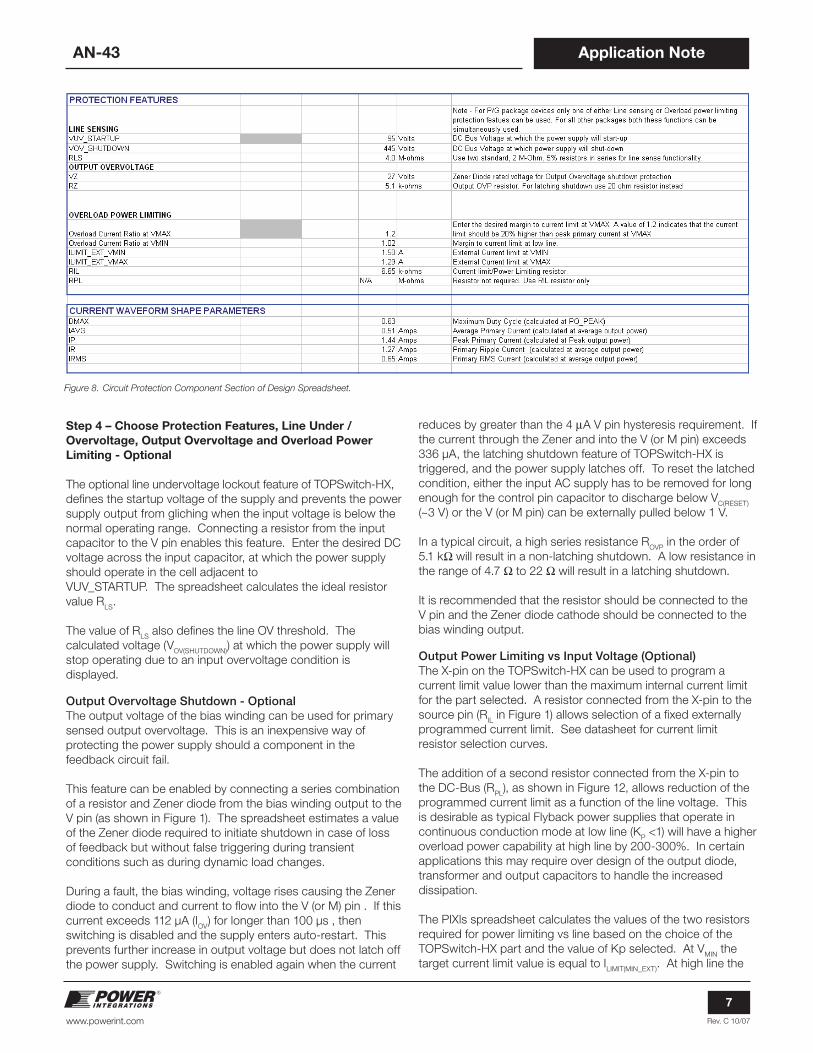
Step 4 – Choose Protection Features, Line Under /
Overvoltage, Output Overvoltage and Overload Power
Limiting - Optional
The optional line undervoltage lockout feature of TOPSwitch-HX,
defi nes the startup voltage of the supply and prevents the power
supply output from gliching when the input voltage is below the
normal operating range. Connecting a resistor from the input
capacitor to the V pin enables this feature. Enter the desired DC
voltage across the input capacitor, at which the power supply
should operate in the cell adjacent to
VUV_STARTUP. The spreadsheet calculates the ideal resistor
value RLS
.
The value of RLS
also defi nes the line OV threshold. The
calculated voltage (VOV(SHUTDOWN)
) at which the power supply will
stop operating due to an input overvoltage condition is
displayed.
Output Overvoltage Shutdown - OptionalThe output voltage of the bias winding can be used for primary
sensed output overvoltage. This is an inexpensive way of
protecting the power supply should a component in the
feedback circuit fail.
This feature can be enabled by connecting a series combination
of a resistor and Zener diode from the bias winding output to the
V pin (as shown in Figure 1). The spreadsheet estimates a value
of the Zener diode required to initiate shutdown in case of loss
of feedback but without false triggering during transient
conditions such as during dynamic load changes.
During a fault, the bias winding, voltage rises causing the Zener
diode to conduct and current to fl ow into the V (or M) pin . If this
current exceeds 112 μA (IOV
) for longer than 100 μs , then
switching is disabled and the supply enters auto-restart. This
prevents further increase in output voltage but does not latch off
the power supply. Switching is enabled again when the current
reduces by greater than the 4 μA V pin hysteresis requirement. If
the current through the Zener and into the V (or M pin) exceeds
336 μA, the latching shutdown feature of TOPSwitch-HX is
triggered, and the power supply latches off. To reset the latched
condition, either the input AC supply has to be removed for long
enough for the control pin capacitor to discharge below VC(RESET)
(~3 V) or the V (or M pin) can be externally pulled below 1 V.
In a typical circuit, a high series resistance ROVP
in the order of
5.1 kΩ will result in a non-latching shutdown. A low resistance in
the range of 4.7 Ω to 22 Ω will result in a latching shutdown.
It is recommended that the resistor should be connected to the
V pin and the Zener diode cathode should be connected to the
bias winding output.
Output Power Limiting vs Input Voltage (Optional)The X-pin on the TOPSwitch-HX can be used to program a
current limit value lower than the maximum internal current limit
for the part selected. A resistor connected from the X-pin to the
source pin (RIL in Figure 1) allows selection of a fi xed externally
programmed current limit. See datasheet for current limit
resistor selection curves.
The addition of a second resistor connected from the X-pin to
the DC-Bus (RPL
), as shown in Figure 12, allows reduction of the
programmed current limit as a function of the line voltage. This
is desirable as typical Flyback power supplies that operate in
continuous conduction mode at low line (KP <1) will have a higher
overload power capability at high line by 200-300%. In certain
applications this may require over design of the output diode,
transformer and output capacitors to handle the increased
dissipation.
The PIXls spreadsheet calculates the values of the two resistors
required for power limiting vs line based on the choice of the
TOPSwitch-HX part and the value of Kp selected. At VMIN
the
target current limit value is equal to ILIMIT(MIN_EXT)
. At high line the
Figure 8. Circuit Protection Component Section of Design Spreadsheet.

Rev. C 10/07
8
Application Note
www.powerint.com
AN-43
target current limit value is calculated based on the value
required for specifi ed PO(PEAK)
multiplied by the margin factor,
Overload Current Limit Ratio at VMAX
. The recommended
value of 120% ensures that the MOSFET protection mode is not
triggered during startup, especially with high output voltage
designs. Lower values are acceptable, but startup into
maximum (peak) load at high input line voltage must be verifi ed.
Resistor values are calculated using the worst case current limit
reduction curves provided in the TOPSwitch-HX datasheet.
Step 5 – Choose Core and Bobbin Based on Output
Power and Enter AE, L
E, A
L, BW, M, L, N
S
Core effective cross-sectional area, AE: (cm2)
Core effective path length, LE: (cm).
Core ungapped effective inductance, AL: (nH/turn2).
Bobbin width, BW: (mm)
Tape margin width equal to half the total margin, M (mm)
Primary Layers, L
Secondary Turns, NS
Core TypeIf the core type cell is left empty, the spreadsheet will default to
the smallest commonly available core suitable for the continuous
(average) output power specifi ed. The entire list of cores
available can be selected from the drop down list in the tool bar
of the PIXls design software.
The grey override cells can be used to enter the core and
bobbin parameters directly. This is useful if a core is selected
that is not on the list, or the specifi c core or bobbin information
differs from that referenced by the spreadsheet.
Table 5 provides a list of commonly available cores and power
levels at which these cores can be used for typical designs.
Safety margin, M (mm)For designs that require safety isolation between primary and
secondary but do not use triple-insulated wire, the width of the
safety margin to be used on each side of the bobbin should be
entered here. For universal input designs, a total windings
margin of 6.2 mm would be required, and a value of 3.1 mm
would be entered into the spreadsheet. For vertical bobbins the
margin may not be symmetrical. However, if a total margin of
6.2 mm were required, then 3.1 mm would still be entered even
if the physical margin were only on one side of the bobbin.
For designs using triple insulated wire, it may still be necessary
to enter a small margin in order to meet the required safety Table
creepage distances. Typically, many bobbins exist for any core
size and, each will have different mechanical spacing. Refer to
the bobbin datasheet or seek guidance from your safety expert
or transformer vendor to determine what specifi c margin is
required.
Figure 9. Transformer Core and Construction Variables Section of Spreadsheet.
Output
Power
66 kHz 132 kHz
Triple
Insulated
Wire
Margin
Wound
Triple
Insulated
Wire
Margin
Wound
EF12.6
EE13
EF16
EE16
EE19
EI22
EI22/19/6
EI22
EE19
EI22/19/6
EEL16
EF20
EI25
EEL19
EF12.6
EE13
EF16
EE16
EI22
EE19
EI22/19/6
EEL160 - 10 W
10 W -
20 W
EF20 EI28
EEL22
EF25
EE19
EI22
EI22/19/6
EF20
EF20
EI25
EEL19
20 W -
30 W
EF25 EI30
EPC30
EEL25
EI28
30 W -
50 W
EI28
EI30
E30/15/7
EER28
E30/15/7
EER28
ETD29
EI35
EI33/29/
13-Z
EER28L
EF25 EEL22
50 W -
70 W
ETD29
EI35
EF32
EF32
ETD34
EI28 EEL25
E30/15/7
EER28
70 W -
100 W
ETD34
E36/18/11
EI40
EI40
E36/18/11
EER35
EI30
E30/15/7
EER28
ETD29
ETD29
EI35
EI33/29/
13-Z
EER28L
EF32
100 W -
150 W
ETD39
EER40
ETD39
EER40
E42/21/15
EI35
EF32
ETD34
ETD34
EI40
E36/18/11
EER35
>150 W
E42/21/15
E42/21/20
E55/28/21
E42/21/20
E55/28/21
E36/18/11
EI40
ETD39
EER40
E42/21/15
E42/21/20
E55/28/21
ETD39
EER40
E42/21/15
E42/21/20
E55/28/21
5. Transformer Core Table.

Rev. C 10/07
9
Application Note
www.powerint.com
AN-43
As the margin reduces the available area for the windings, the
margin format described above may not be suitable for small
core sizes. If after entering the margin, more than 3 primary
layers (L) are required, it is suggested that either a larger core be
selected or switch to a zero margin design approach using
triple-insulated wire.
Primary Layers, LPrimary layers should be in the range of 1 < L < 3, and in
general it should be the lowest number that meets the primary
current density limit (CMA). Values of 100 Cmils/Amp for
designs <5 W scaling linearly to 500 Cmils/Amp at 200 W are
typical in designs without forced air cooling. Designs with more
than 3 layers are possible, but the increased leakage inductance
and issues associated with the physical fi t of the windings
should be considered. A split primary construction may be
helpful for designs where leakage inductance clamp dissipation
is too high. Here half of the primary winding is placed on either
side of the secondary (and bias) winding in a sandwich
arrangement.
Secondary turns, NS
If the grey override cell is left blank, the minimum number of
secondary turns is calculated such that the maximum operating
fl ux density BM is kept below the recommended maximum of
3000 Gauss (300 mT). In general, it is not necessary to enter a
number in the override cell except in designs where a lower
operating fl ux density is desired (see the explanation of BM
limits).
Step 6 – Iterate Transformer Design / Generate
Prototype
Iterate the design making sure that no warnings are displayed.
Any parameters outside the recommended range of values can
be corrected by following the guidance given in the right hand
column.
Once all warnings have been cleared, the output transformer
design parameters can be used to wind a prototype transformer
or sent to a vendor for samples. (See note on transformer
prototying services in Quick Start section.)
The key transformer electrical parameters are:
Primary Inductance, LP (μH)This is the target nominal primary inductance of the transformer.
Primary Inductance Tolerance, LPTOLERANCE(%)This is the assumed primary inductance tolerance. A value of
10% is used by default; however if specifi c information is known
from the transformer vendor, then this may be entered in the
grey override cell.
Number of Primary Turns, NP
For low leakage inductance applications, a split primary
construction may be used, and is recommended for designs
above 20 W.
Gapped Core Effective Inductance, ALG: (nH/N2)Used by the transformer vendor to specify the core center leg air gap.
Maximum Operating Flux Density, BM (Gauss)A maximum value of 3000 Gauss during normal operation is
recommended. This limits transformer core loss and audible
noise generated at light load levels. Under these conditions the
output voltage is low, and little reset of the transformer occurs
during the MOSFET off time. This allows the transformer fl ux
density to staircase above the normal operating level. A value
of 3000 Gauss at the peak current limit of the selected device,
together with the built in protection features of TOPSwitch-HX,
provides suffi cient margin to prevent core saturation under
startup or output short circuit conditions.
The MCM mode of operation used in TOPSwitch-HX can
generate audio frequency components in the transformer,
especially if a long core is used. This audible noise generation
is minimized when a value of 3000 Gauss is used for BM. This
results in an operating fl ux density of 750 Gauss in MCM mode.
Following this guideline and using the standard transformer
production technique of dip varnishing practically eliminate
audible noise. A careful evaluation of the audible noise
performance should be made using production transformer
samples before approving the design. Ceramic capacitors that
use dielectrics, such as Z5U, when used in clamp circuits may
also generate audio noise. If this is the case, a cure may be to
replace them with capacitors having a different dielectric, for
example a polyester fi lm type.
Peak Flux Density, BP (Gauss)A maximum value of 4200 Gauss is recommended to limit the
maximum fl ux density under start up and output short circuit
conditions. This calculation assumes worst-case current limit
and inductance values. In high ambient temperature
applications, such as sealed adapters, this value may need to
be reduced to 3600 Gauss due to the higher operating ambient
temperature. It is important to verify that core saturation does
not occur at maximum ambient temperature under overload
conditions just prior to loss of regulation.
Maximum Primary Wire Diameter, OD (mm)By default, if the override cell is empty, double insulated wire is
assumed and the standard wire diameter is chosen. The grey
override cells can be used to enter the wire diameter directly by
the user.
The other factors automatically calculated by the
spreadsheet include:
Estimated Total Insulation Thickness, INS (mm)Primary wire size, DIA: (mm)Primary wire gauge, AWGNumber of primary layers, LEstimated core center leg gap length: Lg: (mm)Number of secondary turns, Ns
Secondary wire size, DIAs: (mm)Secondary wire gauge, AWG
In multiple output design NSx, CMSx, AWGSx (where x is the
output number) should also be used.

Rev. C 10/07
10
Application Note
www.powerint.com
AN-43
Figure 10. Transformer Primary Design Parameters Section of Spreadsheet.
Figure 11. Transformer Secondary Design Parameters Section of Spreadsheet – Multiple Outputs.

Rev. C 10/07
11
Application Note
www.powerint.com
AN-43
PI-4836-101507
D
S
C
TOPSwitch-HX
CONTROL
V
+
-
FX
VAC
CIN
TL431
UTV817A
VO
470 VO = 12 V)
1 k
3.3 k 100 nF
10 k
R =VO - 2.5
2.5X10 k
Feedback Circuit
+
100 VO = 5 V)CIRCUIT PERFORMANCECircuit Tolerance 1%Load Regulation 0.2%Line Regulation 0.2%
RS2
RS1
RD
CPF
LPF
100 nFOptional
RPL
RBIAS
Figure 12. Typical TOPSwitch-HX Flyback Power Supply Using Optocoupler-TL431 Feedback Circuit.
Figure 13. Universal Input, 35 W Power Supply Using TOP258PN.
D
S
C
M
CONTROL
PI-4747-091407
R1133
R1233
R32.0 M
R1610 k
R1710 k
R2110 k
1%
R18196 k
1%
R1910
R1422R13
330
R151 k
R2012.4 k
1%
D91N4148
U3TL431
2%
VR3BZX55B8V2
8.2 V2%
R7201/2 W
VR21N5250B
20 V
VR1P6KE200A
D5FR106
R42.0 M
R55.1 k
R11 M
R21 M
R86.8
R104.7
R622 k2 W
U2BPS2501-
1-H-A
U2APS2501-
1-H-A
L23.3 H
L16.8 mH
L33.3 H
U1TOP258PN
C947 F16 V C20
10 F50 V
C21220 nF50 V
C191.0 F50 V
C1010 F50 V C11
2.2 nF250 VAC
D6FR106
D8SB530
D7SB560
C8100 nF50 V
D11N4937
D21N4007
D31N4937
D41N4007
C13680 F25 V
C14680 F25 V
C15220 F25 V
C18220 F10 V
C172200 F
10 V
C12470 pF100 V
C16470 pF100 V
2T1
EER28 7
11
9
3
6
5
4
C4100 F400 V
C63.9 nF1 kV
C72.2 nF
250 VAC
C3220 nF
275 VAC
RT110
F13.15 A
TOPSwitch-HX
L
E
N
+12 V,2 A
RTN
+5 V,2.2 A
RTN
tO
90 - 265VAC

Rev. C 10/07
12
Application Note
www.powerint.com
AN-43
Step 7 – Selection of TOPSwitch-HX External Components
Control Pin – External ComponentsThe schematic in Figure 12 shows the external components
required for a typical TOPSwitch-HX power supply design. It is
strongly recommended that a 100 nF capacitor be connected
between the CONTROL pin and the SOURCE pin of the
TOPSwitch-HX. This capacitor should be located adjacent to
the TOPSwitch-HX with short traces. In designs using surface
mount components, this capacitor should be located directly at
the pins of the TOPSwitch-HX.
In addition to the 100 nF capacitor connected to the CONTROL
pin, a series combination of a 6.8 Ω resistor and a 47 μF
electrolytic capacitor is required to be connected between the
CONTROL pin and the SOURCE terminal of the TOPSwitch-HX.
The capacitor provides both timing for auto-restart and, together
with the dynamic impedance Zc of the CONTROL pin, sets the
dominant pole for the control loop. The combination of the
capacitor and series resistor adds a zero to the transfer function
of the control loop, The resulting phase boost at approximately
200 Hz improves the bandwidth of the power supply.
Step 8 – Selection of Line - Undervoltage / Overvoltage
Components
The line undervoltage detection feature prevents the power
supply from starting until the input voltage is above a defi ned
level. During power-up or when the switching of the power
MOSFET is disabled during auto-restart, the current into the EN/
UV pin must exceed 25 μA to initiate switching (lUV
in data sheet).
As a resistor from the DC rail to the V pin is used to sense the
input voltage, the supply voltage that causes the current into the
V pin to exceed 25 μA defi nes the undervoltage threshold. The
resistor connected to the V pin also sets the voltage at which a
line input overvoltage condition will be detected.
The sense resistor should be rated above 400 V, generally
requiring either a single 0.5 W or two 0.25 W devices connected
in series. A typical value of 4 MΩ is suggested for use as line
sense resistor for Universal input applications. Additional
guidance is provided by the design spreadsheet.
If the undervoltage (UV) or the overvoltage (OV) functions are
to be used selectively, a number of circuits are provided in the
TOPSwitch-HX family datasheet to ease the selection of external
components. If the V pin function is not used, the V pin should
be connected to the source pin. The V pin should not be left
unconnected.
Step 9 – Selection of Primary Clamp Components
It is recommended that either a Zener clamp or an RCD
combined with a Zener clamp be used in TOPSwitch-HX
designs. This is to ensure that the peak drain voltage is limited
to below the BVDSS
of the internal MOSFET while still maximizing
effi ciency and minimizing no-load consumption.
A standard RCD clamp designed to limit the peak drain voltage
under peak load conditions represents a signifi cant load as the
output power is reduced, resulting in lower light-load effi ciency
and higher no-load consumption.
Figure 13 shows an example of an optimized clamp
arrangement. The clamp ensures that peak drain voltage is
limited to an acceptable level under worst-case conditions of
maximum input voltage, the overload power or output short
circuit and maximum ambient temperature.
Table 6. List of Diodes Suitable for use as the output rectifi er.
Rec. Diode VR(V) I
D(A) Package Manufacturer
Schottky
1N5819 40 1 Axial General Semi
SB140 40 1 Axial General Semi
SB160 60 1 Axial General Semi
MBR160 60 1 Axial IR
11DQ06 60 1.1 Axial IR
1N5822 40 3 Axial General Semi
SB340 40 3 Axial General Semi
MBR340 40 3 Axial IR
SB360 60 3 Axial General Semi
MBR360 60 3 Axial IR
SB540 40 5 Axial General Semi
SB560 60 5 Axial General Semi
MBR745 45 7.5 TO-220 General Semi / IR
MBR760 60 7.5 TO-220 General Semi
MBR1045 45 10 TO-220 General Semi / IR
MBR1060 60 10 TO-220 General Semi
MBR10100 100 10 TO-220 General Semi
MBR1645 45 16 TO-220 General Semi / IR
MBR1660 60 16 TO-220 General Semi
MBR2045CT 45 20(2×10) TO-220 General Semi / IR
MBR2060CT 60 20(2×10) TO-220 Genreal Semi
MBR20100 100 20(2×10) TO-220 General Semi / IR
UFR
UF4002 100 1 Axial General Semi
UF4003 200 1 Axial General Semi
MUR120 200 1 Axial General Semi
EGP20D 200 2 Axial General Semi
BYV27-200 200 2 Axial General Semi /
Philips
UF5401 100 3 Axial General Semi
UF5402 200 3 Axial General Semi
EGP30D 200 3 Axial General Semi
BYV28-200 200 3.5 Axial General Semi /
Philips
MUR420 200 4 TO-220 General Semi
BYW29-200 200 8 TO-220 General Semi
Philips
BYV32-200 200 18 TO-220 General Semi /
Philips

Rev. C 10/07
13
Application Note
www.powerint.com
AN-43
The peak drain voltage should be limited to a maximum of 650 V
under these conditions to provide a margin for component
variation. In the design shown in Figure 13, the peak drain
voltage was limited to 600 V. The clamp diode (D2) must be a
fast or an ultra-fast recovery type with a reverse recovery time
<500 ns. Under no circumstances should a standard recovery
rectifi er diode be used. The high dissipation that may result
during startup or an output short circuit can cause failure of the
diode. Resistor R13 damps ringing for reduced EMI.
Power supplies using different members of the TOPSwitch-HX
family will have different peak primary currents and leakage
inductances, and therefore different leakage energy. Capacitor
C5 and R17 must be optimized for each design. As a general
rule, minimize the value of capacitor C5 and maximize the value
of resistor R17 while still meeting the recommended 650 V peak
drain voltage limit.
Step 10 – Select Output Rectifi er Diode
For each output use the values of peak inverse voltage (VR) and
output current (IO) provided in the design spreadsheet to select
the output diodes. Table 6 shows some commonly available
types.
VR ≥ 1.25 x PIV
S: where PIVS is taken from the Voltage Stress
Parameters section of the spreadsheet and Transformer
Secondary Design Parameters (Multiple Outputs).
ID ≥ 2 x I
O: where ID is the diode rated DC current, and I
O is the
average output current. Depending on the temperature rise
and the duration of the peak load condition, it may be
necessary to increase the diode current rating once a prototype
has been built. This also applies to the amount of heatsinking
required.
Figure 14. Typical Zener Feedback Circuit.
Figure 15. Optocoupler-TL431 Feedback Circuit.
PI-4837-092107
D
S
C
TOPSwitch-HX
CONTROL
V
+
-
FX
VAC
CIN
DZ
LTV817A
VO
47
Feedback Circuit
+
CIRCUIT PERFORMANCECircuit Tolerance 5%Load Regulation 1%Line Regulation 0.5%
470RD
CPF
LPF
100 nFOptional
RBIAS
Zener2%
* 47 is suitable for VO upto 7.5 V. For VO >7.5 V, a higher value may be required for optimum transient response.**470 is good for Zeners with IZT = 5 mA. Lower values are needed for Zeners with higher IZT. (E.g. 150 for IZT = 20 mA).
PI-4836-092107
D
S
C
TOPSwitch-HX
CONTROL
V
+
-
FX
VAC
CIN
TL431
UTV817A
VO
470 VO = 12 V)
1 k
3.3 k 100 nF
10 k
R =VO - 2.5
2.5X10 k
Feedback Circuit
+
100 VO = 5 V)CIRCUIT PERFORMANCECircuit Tolerance 1%Load Regulation 0.2%Line Regulation 0.2%
RS2
RS1
RD
CPF
LPF
100 nFOptional
RBIAS

Rev. C 10/07
14
Application Note
www.powerint.com
AN-43
Step 11 – Select Output Capacitor
Ripple Current RatingThe spreadsheet calculates output capacitor ripple current using
the average output power. Therefore the actual rating of the
capacitor will depend on the peak to average power ratio of the
design. In most cases this assumption will be valid as capacitor
ripple rating is a thermal limitation, and most peak load durations
are shorter than the thermal time constant of the capacitor
(< 1 s). For such designs, select the output capacitor(s) such
that the ripple rating is greater than the calculated value of IRIPPLE
from the spreadsheet. However, in designs with high peak to
continuous (average) power and long duration peak load
conditions, the capacitor rating may need to be increased based
on the measured capacitor temperature rise under worst-case
load and ambient conditions.
In either case, if a suitable individual capacitor cannot be found,
then two or more capacitors may be used in parallel to achieve a
combined ripple current rating equal to the sum of the individual
capacitor ratings.
Many capacitor manufacturers provide factors that increase the
ripple current rating as the capacitor operating temperature is
reduced from its data sheet maximum. This should also be
considered to ensure that the capacitor is not oversized.
ESR Specifi cationThe switching ripple voltage is equal to the peak secondary
current multiplied by the ESR of the output capacitor. It is
therefore important to select low ESR capacitor types to reduce
the ripple voltage. In general, selecting a capacitor rated for the
output ripple, will result in an acceptable value of ESR.
Voltage RatingSelect a voltage rating such that V
RATED≥1.25 x V
O
Step 12 – Select Feedback Circuit Components
The choice of the feedback circuit for a power supply is
governed by the desired output regulator. A simple feedback
circuit can be confi gured using a Zener diode in series with the
optocoupler diode. Though this method is inexpensive, it relies
on the Zener diode to control the output voltage, which limits
performance due to the device’s typically poor tolerance and
temperature coeffi cient.
Figure 14 shows a typical implementation of Zener feedback.
The drop across the Zener diode DZ, optocoupler series resistor
RFB1
and the optocoupler LED determine the output voltage.
Resistor RBIAS
provides a 1 mA bias current so that the Zener
diode is operating close to its knee voltage. Resistor RFB1 sets
the DC gain of the feedback. Both these can be 0.125 W or
0.25 W, 5% types. Selecting a Zener with a low test current
(lZT
≤ 5 mA) is recommended to minimize the current needed to
bias the feedback network, reducing no-load input power
consumption.
For improved accuracy, Figure 15 shows a typical
implementation using a reference IC. A TL431 is used to set the
output voltage and is programmed via a resistor divider RS1
and RS2. Resistor RBIAS
provides the minimum operating
current for the TL431 while RFB1 sets the DC gain. The 100 nF
capacitor and series resistor roll off the gain of TL431 so that it
does not respond to cycle-by-cycle output ripple voltage. AC
feedback is provided directly through the optocoupler. An RC
circuit placed across the resistor RFB1 can provide additional
phase boost to improve control loop bandwidth.
A post fi lter (LPF
and CPF
) is typically added to reduce high
frequency switching noise and ripple. Inductor LPF
should be in
the range of 1 μH – 3.3 μH with a current rating above the peak
output current. Capacitor CPF
should be in the range of 100 μF
to 330 μF with a voltage rating ≥1.25 x VOUT
. If a post fi lter is
used then the optocoupler should be connected as shown,
before the post fi lter inductor and the sense resistors, after the
post fi lter inductor (when applicable).
Table 7 is a list of commonly used optocouplers for feedback
control of isolated switching power supplies. Use of an
optocoupler with a CTR of 0.8 to 2 is recommended.
P/N CTR(%) BVCEO Manufacturer
4 Pin DIP
PC123Y6 80-160 70 V Sharp
PC817X1 80-160 70 V Sharp
SFH615A-2 63-125 70 V Vishay, Isocom
SFH617A-2 63-125 70 V Vishay, Isocom
SFH618A-2 63-125 55 V Vishay, Isocom
ISP817A 80-160 35 V Vishay, Isocom
LTV817A 80-160 35 V Liteon
LTV816A 80-160 80 V Liteon
LTV123A 80-160 70 V Liteon
K1010A 60-160 60 V Cosmo
6 Pin DIP
LTV702FB 63-125 70 V Liteon
LTV703FB 63-125 70 V Liteon
LTV713FA 80-160 35 V Liteon
K2010 60-160 60 V Cosmo
PC702V2NSZX 63-125 70 V Sharp
PC703V2NSZX 63-125 70 V Sharp
PC713V1NSZX 80-160 35 V Sharp
PC714V1NSZX 80-160 35 V Sharp
MOC8102 73-117 30 V Vishay, Isocom
MOC8103 108-173 30 V Vishay, Isocom
MOC8105 63-133 30 V Vishay, Isocom
CNY17F-2 63-125 70 V Vishay, Isocom,
Liteon
Table 7. Optocouplers.

Rev. C 10/07
15
Application Note
www.powerint.com
AN-43
Figure 16. PCB Layout Example Using P-Package.
Figure 17. PCB Layout Example Using M-package.
+- DCOut
+
-
HV
PI-4753-070307
Y1-Capacitor
C6
Isolation Barrier
OutputRectifier
R1 R2
JP1
J1
C1U1
R3
C2R4
D1
VR
1
C4C3
R8
D2
VR2
C5
C9
D3C7
L1
C8
J2
R8
R13
R14R6
R7
JP2
R12
R11
R10U3
R9C10
T1
Output FilterCapacitor
Input FilterCapacitor
Maximize hatched copper areas ( ) for optimum heat sinking
U2
Transformer
DSS
SS
CM
Optional PCB slot for external heatsink in contact with
SOURCE pins
+- DCOut
+
-HV
PI-4752-070307
Isolation Barrier
OutputRectifier
R1
JP1
J1
C1U1
R5
C2
R6
D1
VR
1
C4R7
C3R8
R9D2
C5
D3
C7
L1
C8
J2R11R
10
JP2
C9
R15
U3
R16
R17
R14
R12
T1
R13
VR2
R2
R3 R4
Output FilterCapacitor
Input FilterCapacitor
Optional PCB slot for external heatsink in contact with
SOURCE pins
Maximize hatched copper areas ( ) for optimum heat sinking
SS D
CXV
SSS
U2
Y1-Capacitor
C6
Transformer

Rev. C 10/07
16
Application Note
www.powerint.com
AN-43
Tips for Designs
Design Recommendations:A soft fi nish circuit is recommended for high output voltage
designs ( > 12 V). This ensures startup with full load at low
line. In Figure 22, R23, D6 and C19 show one implementa-
tion of the soft fi nish circuit.
A 10 μF, 50 V electrolytic capacitor is recommended for the
bias winding output fi lter to ensure appropriate bias voltage
for the optocoupler when the power supply is unloaded. The
bias winding output voltage should be a minimum of 10 V or
higher.
Circuit Board LayoutTOPSwitch-HX is a highly integrated power supply solution that
integrates on a single die both the controller and the high
voltage MOSFET. The presence of high switching currents and
voltages together with analog signals makes it especially
important to follow good PCB design practice to ensure stable
and trouble free operation of the power supply.
When designing a PCB for the TOPSwitch-HX based power
supply, it is important to follow the following guidelines:
Primary Side ConnectionsUse a single point (Kelvin) connection at the negative terminal
of the input fi lter capacitor for the TOPSwitch-HX SOURCE
pin and bias winding return. This improves surge capabilities
by returning surge currents from the bias winding directly to
the input fi lter capacitor.
•
•
•
The CONTROL pin bypass capacitor should be located as
close as possible to the SOURCE and CONTROL pins and its
SOURCE connection trace should not be shared by the main
MOSFET switching currents or bias winding return connection.
All SOURCE pin referenced components connected to the
MULTI-FUNCTION (M), VOLTAGE MONITOR (V) or EXTERNAL
CURRENT LIMIT (X) pins should also be located closely
between that pin and the SOURCE pin. The SOURCE
connection trace of these components should not be shared
by the main MOSFET switching or bias winding return
currents. It is very critical that the SOURCE pin switching
current is returned to the input capacitor negative terminal
through a separate trace that is not shared by the compo-
nents connected to CONTROL, MULTI-FUNCTION,
VOLTAGE-MONITOR or EXTERNAL CURRENT LIMIT pins.
This is because the SOURCE pin is also the controller ground
reference pin. Any traces to the M, V or X pins should be kept
as short as possible and physically away from the DRAIN
node, clamp components or any node with high di/dt or
dv/dt, to prevent noise coupling.
The LINE-SENSE resistor should be located close to the M or
V pin to minimize the trace length on the high impedance M or
V pin side. The DC bus side of the V pin resistor should be
connected as close to the bulk capacitor as possible.
In addition to the 47 μF CONTROL pin capacitor, a high
frequency 0.1 μF bypass capacitor in parallel should be used
for local decoupling (C4 in Figures 16, 17 and 18).
The feedback optocoupler output should be routed away from
any high voltage or high current traces to prevent noise
coupling.
•
•
•
•
•
Figure 18. PCB Layout Example Using Y-package.
+- DCOut
+
-HV
PI-4751-070307
Y1-Capacitor
C6
Isolation Barrier
OutputRectifier
R1 R2
R3 R4
JP1
J1
C1
U1HS1
R3
C2
R4
D1
VR
1
C4
R7 R10R13
D2
VR2
C5 C9
D3
C7
L1
C8
J2
R9
R11
R16 R
14
R8
JP2
R12R17
R15
U3
R12
C10
T1
Output FilterCapacitor
Input FilterCapacitor
Transformer
S F
C
X V
D
U2

Rev. C 10/07
17
Application Note
www.powerint.com
AN-43
Y-CapacitorThe preferred Y-capacitor connection is close to the transformer
secondary output return pin(s) and the positive primary DC input
pin of the transformer. If the Y capacitor is connected between
primary and secondary RTN, then the primary connection
should be made via a dedicated trace from the Y-capacitor to
the negative input capacitor terminal. This ensures that surge
currents across the isolation barrier are routed away from traces
connected to the TOPSwitch-HX.
SecondaryTo minimize leakage inductance and EMI, the area of the loop
connecting the secondary winding, the output diode and the
output fi lter capacitor should be minimized. In addition, suffi cient
copper area should be provided at the anode and cathode
terminal of the diode for heatsinking. A larger area is preferred at
the quiet cathode terminal as a large anode area can increase
high frequency radiated EMI.
Figure 19. Layout Considerations (Shown Schematically) and Common Mistakes.
D
S
CCONTROL
V
PI-4838-092407
TOPSwitch-HX
X F
CLAMP
RLS
RIL
B+
PRI RTN
Preferred Y capacitor placement(B+ to output RTN)
Y capacitor and bias return connected with dedicated tracedirectly to PRI RTN at input capacitor
Line sense resistor (RLS) connected at input capacitor
RLS placed physicallyclose to V-pin
RIL placed physicallyclose to X-pin
Kelvin connect at SOURCE pin, no power currents flow in signal traces
CONTROL pin decoupling capacitor placed directly between CONTROL and SOURCE pins
For correct device operation ensure that good layout practices are followed
D
S
C
V
CONTROL
PI-4839-092407
TOPSwitch-HX
X F
CLAMP
IBIAS
B+
PRI RTN
Bias winding return and primary to secondary displacement currents (via CY2)flow through signal traces.Voltage drop ( VS) across trace impedances modulates source reference of controller
VS
CY2
CY1
ICY2+
Poor layout may cause higher output ripple or prevent proper device operation
D
S
C
V
CONTROL
PI-4840-092407
TOPSwitch-HX
X F
CLAMP
VS
Without Kelvin connection at SOURCE pin, power current (IS) creates voltage drop in trace ( VS), which modulates source reference of controller
B+
PRI RTNIS
Poor layout may cause higher output ripple or prevent proper device operation
D
S
C
V
CONTROL
PI-4841-092407
TOPSwitch-HX
X F
CLAMP
RLS
PRI RTN
B+
IB+
VB+
V-pin trace routed in close proximity to drain node causing noise coupling
RLS placed away from device. Increases V-pin node area, increasing potential noise coupling
Voltage drop across trace impedance ( VB+)modulates V-pin current
Poor layout may cause changes in UV/OV thresholds and higher output ripple
✓ Recommended Layout ✘ Poor Bias Winding Return Connection
✘ Poor Signal Source Connection ✘ Poor Line Sense Resistor Location and Connection

Rev. C 10/07
18
Application Note
www.powerint.com
AN-43
Figure 20. Primary Sensed OVP circuit for TOPSwitch-HX based Flyback
Power Supply.Figure 21. Primary Sensed Overvoltage Protection Circuit for a Flyback
Power Supply Using TOPSwitch-HX with Additional V-pin
Noise Decoupling.
Common Layout Problems to AvoidA poor layout will often result in performance issues that may
be time consuming to analyze, and they may occur at the end
of development, when PCB design changes are diffi cult. Figure
19 will help quickly identify the root cause of a problem and
correct the layout. The fi gure schematically shows common
layout mistakes and the reasons they should be avoided
Implementing Overvoltage Protection Feature Using the TOPSwitch-HX
The bias winding output tracks the changes in the output
voltage for the fl yback topology. If the feedback loop fails and
results in an increase in output voltage, the output voltage of
the bias winding will also increase. This can be used to detect
an output overvoltage condition.
A suitable Zener diode with a series resistor connected
between the bias winding output and the V pin can be selected
such that the Zener diode conducts once the bias winding
voltage rises signifi cantly (typically 20 % to 30 %) above the
highest voltage at the output of the bias winding during normal
operation (or under a transient loading condition during normal
operation). A current injected in the V-pin in excess of 112 μA
will result in the switching cycle being terminated
instantaneously. If the injected current remains higher than
112 μA for over 100 μS, the part will enter hysteretic OV
shutdown. In such a situation, switching will resume as soon
as the injected current reduces below the hysteresis point after
completing an auto-restart cycle.
If the injected current exceeds 112 uA, the V-pin responds by
dropping the V-pin voltage by 0.5 V. If the drop in V-pin voltage
causes the V-pin current to jump to a value higher than 336 uA,
the part enters a state of latched shutdown. In this state the
operation will not resume unless input is cycled and the C-pin
capacitor is allowed to discharge, thereby resetting the part. In
addition the latched state may be reset by pulling the V-pin
below 1 V with an external transistor. Care must be taken when
designing external circuits connected to the V-pin. The V-pin
operates at very low currents to reduce no-load power
consumption. This results in the V pin node having a relatively
high impedance, and it is therefore susceptible to noise. See
the layout guidline section for more detailed information.
PI-4822-092107
D
S
CCONTROL
URYS YURYS
V
FX
UELDV
PI-4821-092107
D
S
CCONTROL
ROVP VROVP
V
FX
RBIAS1N4148
100 nF
0 to 47 W
If the value of the series resistor ROVP is very small (in the range
of 5 ohm to 22 ohm), the change of V-pin voltage in response to
the injected current reaching 112 uA is often adequate to cause
a current in excess of 336 uA to fl ow which results in latched
overvoltage condition, requiring a reset.
In some designs the Zener diode connected from the bias
winding may become a source of noise injected into the V-pin.
This happens when the bias winding output ripple is high, or
the circuit board layout allows noise from adjacent circuits to
be coupled in the trace connecting the Zener diode to the
V-pin. In such a situation, the solution shown in Figure 21
should be used.
The circuit shown in Figure 21 is also useful in situations where
it is diffi cult to achieve a latched shutdown due to slow rise in
power supply and bias winding output voltages after the
feedback loop opens. Power supplies with large output
capacitance and/or high output load may have this issue
during an open loop fault. If necessary, RBIAS
can be added to
provide additional fi ltering of the bias output to prevent false
triggering of the OVP threshold.
Quick Design Checklist
As with any power supply, all TOPSwitch-HX designs should be
verifi ed with actual hardware to ensure that component
specifi cations are not exceeded under worst-case conditions.
The following minimum set of tests is strongly recommended:
Maximum drain voltage – Verify that peak VDS
does not
exceed 675 V at highest input voltage and maximum
overload output power. Maximum overload output power
occurs when the output is overloaded to a level just before
the power supply goes into auto-restart (loss of regulation).
Maximum drain current – At maximum ambient temperature,
maximum input voltage and maximum output load, verify
drain current waveforms at start-up for any signs of trans-
former saturation and excessive leading edge current spikes.
TOPSwitch-HX has a minimum leading edge blanking time of
180 ns to prevent premature termination of the ON-cycle.
Verify that the leading edge current spike is below the
allowed current limit envelope for the drain current waveform
at the end of the 180 ns minimum blanking period.
1.
2.

Rev. C 10/07
19
Application Note
www.powerint.com
AN-43
Figure 22. 150 W, 19.5 V Power Supply using TOP258YN.
Thermal check – At maximum output power, minimum input
voltage and maximum ambient temperature; verify that
temperature limits are not exceeded for the TOPSwitch-HX,
transformer, output diodes and output capacitors. Enough
thermal margin should be allowed for the part-to-part
variation in the RDS(ON)
of TOPSwitch-HX, as specifi ed in the
data sheet. A maximum source pin temperature for the P/G
and M packages or tab temperature for Y package of 110 °C
is recommended to allow for these variations. Alternatively,
the design margin can be verifi ed by connecting an external
resistance that is in series with the DRAIN pin and is attached
to the same heat sink. The resistance selected would be
equal to the difference between the measured RDS(ON) of
the device under test and the worst case maximum specifi -
cation.
Appendix A
Application Examples
A High Effi ciency, 150 W, 250 – 380 VDC Input Power
Supply
The circuit shown in Figure 22 delivers 150 W (19 V at 7.7 A) at
84% effi ciency using a TOP258YN from a 250 VDC to 380 VDC
input. A DC input is shown, as typically at this power level a
power factor correction stage would precede the power supply.
Capacitors C1 and C2 provide local decoupling, necessary
when the supply is remote from the main PFC output capacitor.
3. Flyback topology is still usable at this power level due to the
high output voltage, keeping the secondary peak currents low
enough to ensure that the output diode and capacitors are
reasonably sized. In this example, the TOP258YN is at the
upper limit of its power capability.
Resistors R3, R6 and R7 provide power limiting, maintaining
relatively constant overload power with input voltage. Line
sensing is implemented by connecting a 4 MΩ resistor from the
V pin to the DC rail. Resistors R4 and R5 together form the
4 MΩ line sense resistor. If the DC input rail rises above
450 VDC, then TOPSwitch-HX will stop switching until the
voltage returns to normal, preventing device damage.
Due to the high primary current, a low leakage inductance
transformer is essential. Therefore, a sandwich winding with a
copper foil secondary is used. Even with this technique, the
leakage inductance energy is beyond the power capability of a
simple Zener clamp. Therefore, R1, R2 and C3 are added in
parallel to VR1 and VR3, two series Zener diodes being used to
reduce dissipation. During normal operation, very little power is
dissipated by VR1 and VR3, the leakage energy instead being
dissipated by R1 and R2. However, VR1 and VR3 are essential
to limit the peak drain voltage during start-up and/or overload
conditions to below the 700 V rating of the TOPSwitch-HX
MOSFET. The schematic shows an additional snubber circuit,
consisting of R20, R21, R22, D5 and C18. This reduces turn-off
losses in the TOPSwitch-HX.
L1
D41N4148
C11100 nF50 V
+19 V, 7.7 A
RTN
RT15
R194.7
D3MBR20100CTR7
4.7 M
D2MBR20100CT
C15-C16820 F25 V
C1447 pF1 kV
R201.5 k2 W
C1047 F10 V
D1BYV26C
T1EI35
11
4
13,14
5
12
1
9,10
7
R154.75 k
1%
C201.0 F50 V
C1747 pF1 kV
C910 F50 V
R2315 k
0.125 W
R1422
0.5 W
R38.06 k
1%
C4
2.2 nF250 VAC
R106.8
C34.7 nF1 kV
C122 F400 V
R221.5 k
2 W
D61N4148
R84.7
R168 k2 W
F14 A
C18120 pF1 kV
R1631.6 k
1%
R268 k
2 W
VR21N5258B
36 V
R111 k
0.125 W
C1910 F50 V
R12240
0.125 W
U1TOP258YN
R2430
0.125 W
C5-C8
25 V
VR1, VR3P6KE100A
R18220.5 W
R21
2 W
D51N4937
U2PC817A
U3TL431
2%
C124.7 nF50 V
R175621%
R1356 k
0.125 W
C13100 nF
50 V
U2PC817B
3.3 HR4
2.0 M
R52.0
1.5 k
tO
TOPSwitch-HX
R64.7 M
820 F 250 - 380
VDC
PI-4795-092007
D
S
C
V
FX
CONTROL

Rev. C 10/07
20
Application Note
www.powerint.com
AN-43
The secondary is rectifi ed and smoothed by D2, D3 and C5,
C6, C7 and C8. Two windings are used and rectifi ed with
separate diodes D2 and D3 to limit diode dissipation. Four
capacitors are used to ensure their individual maximum ripple
current limits are not exceeded. Inductor L1 and capacitors
C15 and C16 provide switching noise fi ltering.
Output voltage is controlled using a TL431 reference IC.
Resistor R15, R16 and R17 form a potential divider to sense the
output voltage. Resistor R12 and R24 together limit the
optocoupler LED current and set overall control loop DC gain.
Control loop compensation is achieved using additional
components, C12, C13, C20 and R13. Diode D6 and capacitor
C19 form a soft fi nish network. This feeds current into the
control pin prior to output regulation, preventing output
overshoot and ensuring startup under low line, full load
conditions.
Suffi cient heat sinking is required to keep the TOPSwitch-HX
device below 110 οC when operating under full load, low line
and maximum ambient temperature. Airfl ow may also be
required if a large heat sink area is not acceptable.
A High Effi ciency, 20 W continuous – 80 W Peak,
Universal Input Power Supply
The circuit shown in Figure 23 takes advantage of several of
TOPSwitch-HX features to reduce system cost, power supply
size and improve power supply effi ciency while delivering
signifi cant peak power. This design delivers 20 W continuous
and 80 W peak at 32 V from an 85 VAC to 265 VAC input. A
nominal effi ciency of 82% at full load is achieved using
TOP258MN.
Figure 22. 20 W Continuous, 80 W Peak, Universal Input Power Supply.
The M-package part has an optimized current limit to enable
design of power supplies capable of delivering high power for
a short duration.
Resistor R12 programs the current limit of the TOPSwitch-HX.
Resistors R11 and R14 provide a signal that reduces the current
limit with increasing DC bus voltage, thereby maintaining a
constant overload power level with increasing line voltage.
Resistors R1 and R2 implement the line undervoltage and
overvoltage function and also provide feed forward
compensation for reducing line frequency ripple in output. The
overvoltage feature stops TOPSwitch-HX switching during a line
surge, extending the high voltage withstand voltage to 700 V
without device damage.
The snubber circuit comprising VR7, R17, R25, C5 and D2 limits
the maximum drain voltage and dissipates energy stored in the
leakage inductance of transformer T1. This clamp confi guration
maximizes energy effi ciency by preventing C5 from discharging
below the value of VR7 during the lower frequency operating
modes of TOPSwitch-HX. Resistor R25 damps high frequency
ringing for reduced EMI.
A combined output overvoltage and over power protection
circuit is provided via the latching shutdown feature of
TOPSwitch-HX and R20, C9, R22 and VR5. Should the bias
winding output voltage across C13 rise due to output overload
or an open loop fault (optocoupler failure), then VR5 conducts,
triggering the latching shutdown. To prevent false triggering
due to short duration overload, a delay is provided by R20,
R22 and C9.
C81 nF
250 VAC
D6-D7
C91 F
100 V
R171 k0.5 W
VR7BZY97C150
150 V
T1
D21N4007GP
D131N4007
F13.15 A
C30100 nF400 V Q3
2N3904
R23
1 M
C1220 nF
275 VAC
90 - 264 VAC
R24
1 M
L15.3 mH
68 k
D101N4007
C3120 F400 V
R113.6 M
D81N4007
RT110
R12 M
R143.6 M
D91N4007
Q22N3904
R1839 k
Q12N3904
R22 M
R32 M
R151 k
R211 M
0.125 WR42 M
R26
C
S
D V
X
R222 M
C6100 nF50 V
U4TOP258MN
C747 F16 V
VR51N5250B
20 V
R25
C510 nF1 kV
R66.8
C101 nF
250 VAC
EF25
R20130 k
D5LL4148
C1310 F50 V
U2APC817D
R92 k
R81.5 k
R1056
VR31N5255B
28 V
C28330 nF50 V
R19680.5 W
STPS3150
C26100 pF1 kV
L3
47 H
L2
3.3 H
C3122 F50 V
C20330 F
50 V
R127.5 k
1%
D111N4007
100
CONTROL
C29220 nF50 V
to
32 V625 mA, 2.5 APK
RTN
PI-4793-091207
1
9
10
5
2
3
4
NC
TOPSwitch-HX

Rev. C 10/07
21
Application Note
www.powerint.com
AN-43
To reset the supply following a latching shutdown, the V pin
must fall below the reset threshold. To prevent the long reset
delay associated with the input capacitor discharging, a fast
AC reset circuit is used. The AC input is rectifi ed and fi ltered by
D13 and C30. While the AC supply is present, Q3 is on and
Q1 is off, allowing normal device operation. However when
AC is removed, Q1 pulls down the V pin and resets the latch.
The supply will then return to normal operation when AC is
again applied.
Transistor Q2 provides an additional lower UV threshold to the
level programmed via R1, R2 and the V pin. At low input AC
voltage, Q2 turns off, allowing the X pin to fl oat, and thereby
disables switching.
A simple feedback circuit automatically regulates the output
voltage. Zener VR3 sets the output voltage together with the
voltage drop across series resistor R5, which sets the DC gain
of the circuit. Resistors R10 and C28 provide a phase boost to
improve loop bandwidth.
Diode D6 is a low loss Schottky rectifi er, and capacitor C20 is
the output fi lter capacitor. Inductor L3 is a common mode
inductor to limit radiated EMI when long output cables are
used and the output return is connected to safety earth ground.
Examples of this include PC peripherals such as inkjet printers.
A High Effi ciency, 35 W, Dual Output - Universal Input
Power Supply
The circuit in Figure 24 takes advantage of several of the
Figure 24. Universal Input, 35W Power Supply Using TOP258PN.
TOP Switch-HX features to reduce system cost and power
supply size and to improve effi ciency. This design delivers
35 W total output power from a 90 VAC to 265 VAC input at an
ambient of 50º C in an open frame confi guration. A nominal
effi ciency of 84 % at full load is achieved using TOP258PN.
With a DIP-8 package, this design provides 35 W continuous
output power using only the copper area on the circuit board
underneath the part as heat sink. The different operating
modes of the TOPSwitch-HX provide signifi cant improvement in
the no-load, standby, and light load performance of the power
supply as compared to previous generations of TOPSwitch.
Resistors R1 and R2 provide line sensing, setting UV at 95 VDC
and OV at 445 VDC.
Diode D5, together with resistors R7, R6, capacitor C6 and
Zener VR1, forms a clamp network that limits the drain voltage
after the MOSFET inside the TOPSwitch turns OFF. Zener VR1
provides a defi ned maximum clamp voltage and typically only
conducts during fault conditions such as overload. This allows
the RCD clamp (R6, R7, C6 and D5) to be sized for normal
operation, thereby maximizing effi ciency at light load.
Should the feedback circuit fail, output of the power supply will
exceed regulation limits. This increased voltage at output will
also result in an increased voltage at the output of the bias
winding. Zener VR2 will break down, and current will fl ow into
the “M” pin of the TOPSwitch, initiating hysteretic overvoltage
protection. Resistor R5 will limit the current into the M pin; if
latching OVP is desired, the value of R5 can be reduced to 20 Ω.
D
S
C
M
CONTROL
PI-4747-091407
R1133
R1233
R32.0 M
R1610 k
R1710 k
R2110 k
1%
R18196 k
1%
R1910
R1422R13
330
R151 k
R2012.4 k
1%
D91N4148
U3TL431
2%
VR3BZX55B8V2
8.2 V2%
R7201/2 W
VR21N5250B
20 V
VR1P6KE200A
D5FR106
R42.0 M
R55.1 k
R11 M
R21 M
R86.8
R104.7
R622 k2 W
U2BPS2501-
1-H-A
U2APS2501-
1-H-A
L23.3 H
L16.8 mH
L33.3 H
U1TOP258PN
C947 F16 V C20
10 F50 V
C21220 nF50 V
C191.0 F50 V
C1010 F50 V C11
2.2 nF250 VAC
D6FR106
D8SB530
D7SB560
C8100 nF50 V
D11N4937
D21N4007
D31N4937
D41N4007
C13680 F25 V
C14680 F25 V
C15220 F25 V
C18220 F10 V
C172200 F
10 V
C12470 pF100 V
C16470 pF100 V
2T1
EER28 7
11
9
3
6
5
4
C4100 F400 V
C63.9 nF1 kV
C72.2 nF
250 VAC
C3220 nF
275 VAC
RT110
F13.15 A
TOPSwitch-HX
L
E
N
+12 V,2 A
RTN
+5 V,2.2 A
RTN
tO
90 - 265VAC

Rev. C 10/07
22
Application Note
www.powerint.com
AN-43
Output voltage is controlled using the amplifi er TL431. Diode
D9, capacitor C20 and resistor R16 form the soft fi nish circuit.
At start, capacitor C20 is discharged. As the output voltage
starts rising, current fl ows through the optocoupler diode inside
U2A, resistor R13 and diode D9 to charge capacitor C20. This
provides feedback to the primary circuit. The current in the
optocoupler diode U2A gradually decreases as the capacitor
C20 becomes charged and the control amplifi er IC U3
becomes operational. This ensures that the output voltage
increases gradually and settles to the fi nal value without any
overshoot. Diode D9 ensures that the capacitor C23 is
maintained charged at all times after startup, which effectively
isolates C20 from the feedback circuit after start-up. Capacitor
C23 discharges via R16 when the power supply shuts down.
Resistor R18, R20 and R21 form a voltage divider network.
The output of this divider network is primarily dependent on the
divider circuit formed using R20 and R21 but modifi ed by
changes in voltage at the 15 V output due to the connection of
resistor R18 to the output of the divider network.
Resistor R19 and VR3 improve cross regulation in case only the
5 V output is loaded, which results in the 12 V output operating
at the higher end of the specifi cation.
Appendix B
Multiple Output Flyback Power Supply Design
The only difference between a multiple output fl yback power
supply and a single output fl yback power supply of the same
total output power is on the secondary side design.
Design with Lumped Output PowerA simple multiple output fl yback design is described in detail in
AN-22, “Designing Multiple Output Flyback Power Supplies with
TOPSwitch.” The design method starts with a single output
equivalent by lumping output power of all outputs to one main
output. Secondary peak current ISP and RMS current ISRMS
are
derived. Output average current IO, corresponding to the
lumped power, is also calculated.
Assumption for Simplifi cationThe current waveforms in the individual output windings are
determined by the impedance in each circuit, which is a
function of leakage inductance, rectifi er characteristics,
capacitor value and output load. Although this current wave-
form may not be exactly the same from output to output, it is
reasonable to assume that, to the fi rst order, all output currents
have the same shape as for the single output equivalent of
combined circuit.
Output RMS Current vs. Average CurrentThe output average current is always equal to the DC load
current, while the RMS value is determined by current wave
shape. Since the current wave shapes are assumed to be the
same for all outputs, their ratio of RMS to average currents must
also be identical. Therefore, with the output average current
known, the RMS current for each output winding can be
calculated as
where ISRMS(n)
and IO(n)
are the secondary RMS current and
output average current of the nth output, and ISRMS
and IO are the
secondary RMS current and output average current for the
lumped single output equivalent design.
Customization of Secondary Designs for Each Output
The turns for each secondary winding are calculated based on
the respective output voltage VO(n)
:
Output rectifi er maximum inverse voltage is
With output RMS current ISRMS(n)
, secondary number of turns
NS(n)
and output rectifi er maximum inverse voltage PIVS(n)
known,
the secondary side design for each output can now be carried
out exactly the same way as for the single output design.
Secondary Winding Wire SizeThe TOPSwitch-HX design spreadsheet assumes a CMA of 200
when calculating secondary winding wire diameters. This gives
the minimum wire sizes required for the RMS currents of each
output using separate windings. Designers may wish to use
larger size wire for better thermal performance. Other
considerations, such as skin effect and bobbin coverage, may
suggest the use of a smaller wire by using multiple strands
wound in parallel. In addition, practical considerations in
transformer manufacturing may also dictate the wire size.
ISRMS n] g= IO n] g# IOISRMS
NS n] g= NS# V+VDVO n] g+VD n] g
PIVS n] g= VMAX# NPNS n] g +VO n] g

Rev. C 10/07
23
Application Note
www.powerint.com
AN-43

For the latest updates, visit our website: www.powerint.comPower Integrations reserves the right to make changes to its products at any time to improve reliability or manufacturability. Power
Integrations does not assume any liability arising from the use of any device or circuit described herein. POWER INTEGRATIONS MAKES
NO WARRANTY HEREIN AND SPECIFICALLY DISCLAIMS ALL WARRANTIES INCLUDING, WITHOUT LIMITATION, THE IMPLIED
WARRANTIES OF MERCHANTABILITY, FITNESS FOR A PARTICULAR PURPOSE, AND NON-INFRINGEMENT OF THIRD PARTY RIGHTS.
Patent Information
The products and applications illustrated herein (including transformer construction and circuits external to the products) may be covered by
one or more U.S. and foreign patents, or potentially by pending U.S. and foreign patent applications assigned to Power Integrations. A
complete list of Power Integrations patents may be found at www.powerint.com. Power Integrations grants its customers a license under
certain patent rights as set forth at http://www.powerint.com/ip.htm.
Life Support Policy
POWER INTEGRATIONS PRODUCTS ARE NOT AUTHORIZED FOR USE AS CRITICAL COMPONENTS IN LIFE SUPPORT DEVICES OR
SYSTEMS WITHOUT THE EXPRESS WRITTEN APPROVAL OF THE PRESIDENT OF POWER INTEGRATIONS. As used herein:
A Life support device or system is one which, (i) is intended for surgical implant into the body, or (ii) supports or sustains life, and (iii)
whose failure to perform, when properly used in accordance with instructions for use, can be reasonably expected to result in signifi cant
injury or death to the user.
A critical component is any component of a life support device or system whose failure to perform can be reasonably expected to cause
the failure of the life support device or system, or to affect its safety or effectiveness.
The PI logo, TOPSwitch, TinySwitch, LinkSwitch, DPA-Switch, PeakSwitch, EcoSmart, Clampless, E-Shield, Filterfuse, StakFET, PI Expert
and PI FACTS are trademarks of Power Integrations, Inc. Other trademarks are property of their respective companies.
©2007, Power Integrations, Inc.
1.
2.
Power Integrations Worldwide Sales Support Locations
World Headquarters5245 Hellyer Avenue
San Jose, CA 95138, USA.
Main: +1-408-414-9200
Customer Service:
Phone: +1-408-414-9665
Fax: +1-408-414-9765
e-mail: [email protected]
China (Shanghai)Rm 807-808A
Pacheer Commercial Centre,
555 Nanjing Rd. West
Shanghai, P.R.C. 200041
Phone: +86-21-6215-5548
Fax: +86-21-6215-2468
e-mail: [email protected]
China (Shenzhen)Rm A, B & C 4th Floor, Block C,
Electronics Science and
Technology Bldg., 2070
Shennan Zhong Rd,
Shenzhen, Guangdong,
China, 518031
Phone: +86-755-8379-3243
Fax: +86-755-8379-5828
e-mail: [email protected]
GermanyRueckertstrasse 3
D-80336, Munich
Germany
Phone: +49-89-5527-3910
Fax: +49-89-5527-3920
e-mail: [email protected]
India#1, 14th Main Road
Vasanthanagar
Bangalore-560052 India
Phone: +91-80-4113-8020
Fax: +91-80-4113-8023
e-mail: [email protected]
ItalyVia De Amicis 2
20091 Bresso MI
Italy
Phone: +39-028-928-6000
Fax: +39-028-928-6009
e-mail: [email protected]
JapanKosei Dai-3 Bldg.
2-12-11, Shin-Yokomana,
Kohoku-ku
Yokohama-shi Kanagwan
222-0033 Japan
Phone: +81-45-471-1021
Fax: +81-45-471-3717
e-mail: [email protected]
KoreaRM 602, 6FL
Korea City Air Terminal B/D, 159-6
Samsung-Dong, Kangnam-Gu,
Seoul, 135-728, Korea
Phone: +82-2-2016-6610
Fax: +82-2-2016-6630
e-mail: [email protected]
Singapore51 Newton Road
#15-08/10 Goldhill Plaza
Singapore, 308900
Phone: +65-6358-2160
Fax: +65-6358-2015
e-mail: [email protected]
Taiwan5F, No. 318, Nei Hu Rd., Sec. 1
Nei Hu Dist.
Taipei, Taiwan 114, R.O.C.
Phone: +886-2-2659-4570
Fax: +886-2-2659-4550
e-mail: [email protected]
Europe HQ1st Floor, St. James’s House
East Street, Farnham
Surrey GU9 7TJ
United Kingdom
Phone: +44 (0) 1252-730-141
Fax: +44 (0) 1252-727-689
e-mail: [email protected]
Applications HotlineWorld Wide +1-408-414-9660
Applications FaxWorld Wide +1-408-414-9760
Revision Notes Date
A Initial Release 9/07
B Text changes 9/07
C Style, formatting and renumbering 10/07
Top Related