


Languages
Pages
Legal

Analog Circuit Design with Submicron Transistors © 2004 B. Boser 1
Analog Circuit Design with Submicron Transistors
Bernhard BoserUC Berkeley
Department of Electrical Engineering and Computer [email protected]

Analog Circuit Design with Submicron Transistors © 2004 B. Boser 2
Analog Circuit Design
• Objective:Translate circuit specifications(gain, bandwidth, dynamic range, …)into transistor sizes and bias currents
• Challenge:Accurate device models for deep submicron transistors– “Square-law model”– Simulation models (BSIM, EVK, …)– “Model” for analog design
Analog Circuit Design with Submicron Transistors © 2004 B. Boser 3
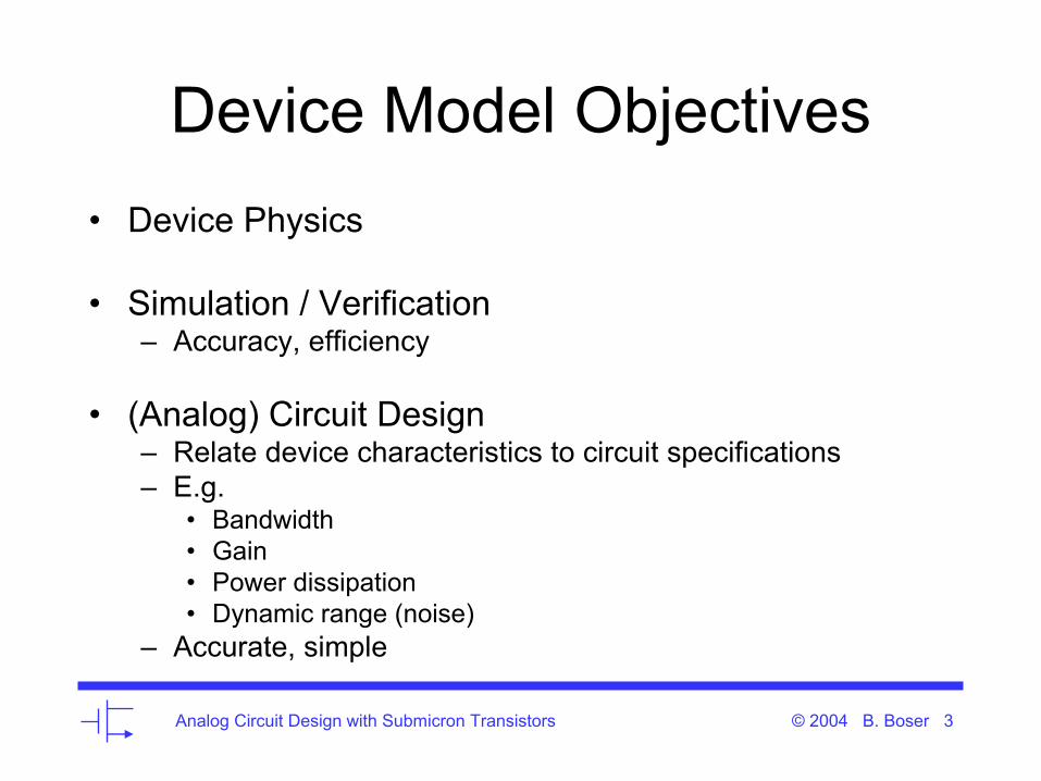
Device Model Objectives• Device Physics
• Simulation / Verification– Accuracy, efficiency
• (Analog) Circuit Design– Relate device characteristics to circuit specifications– E.g.
• Bandwidth• Gain• Power dissipation• Dynamic range (noise)
– Accurate, simple
Analog Circuit Design with Submicron Transistors © 2004 B. Boser 4
Device Parameters for Analog Design
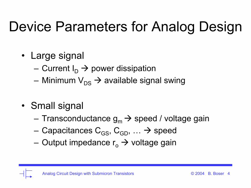
• Large signal– Current ID power dissipation– Minimum VDS available signal swing
• Small signal– Transconductance gm speed / voltage gain– Capacitances CGS, CGD, … speed– Output impedance ro voltage gain
Analog Circuit Design with Submicron Transistors © 2004 B. Boser 5
Metrics for Design
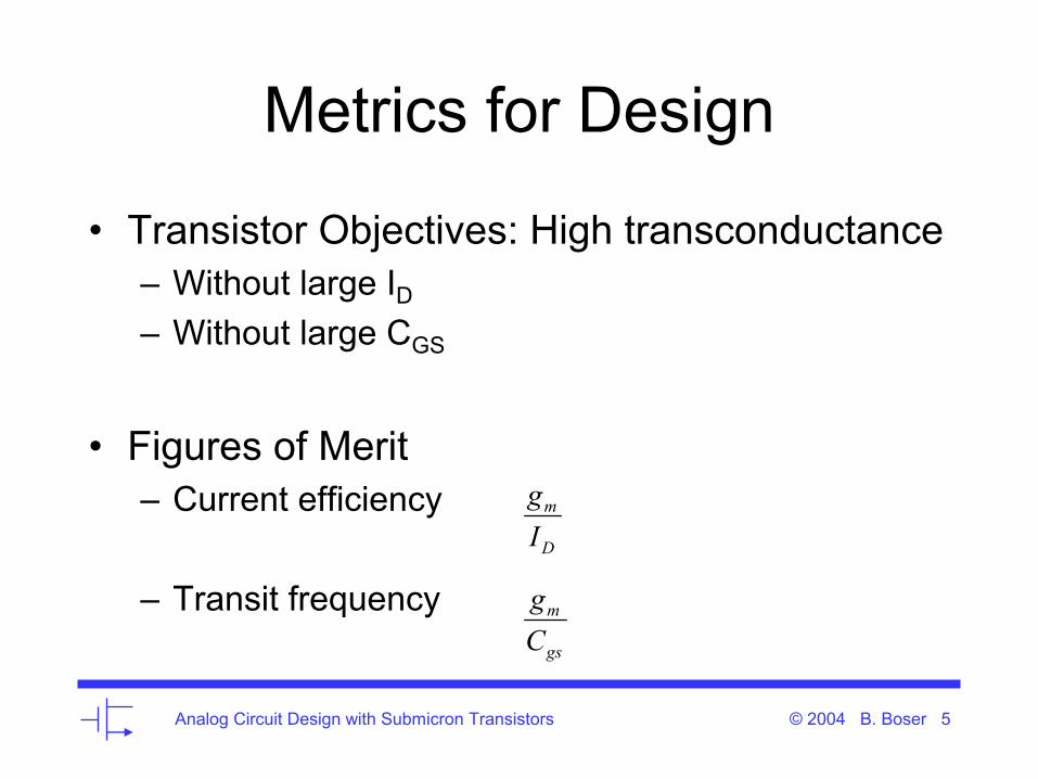
• Transistor Objectives: High transconductance– Without large ID– Without large CGS
• Figures of Merit – Current efficiency
– Transit frequencyD
m
Ig
gs
m
Cg
Analog Circuit Design with Submicron Transistors © 2004 B. Boser 6
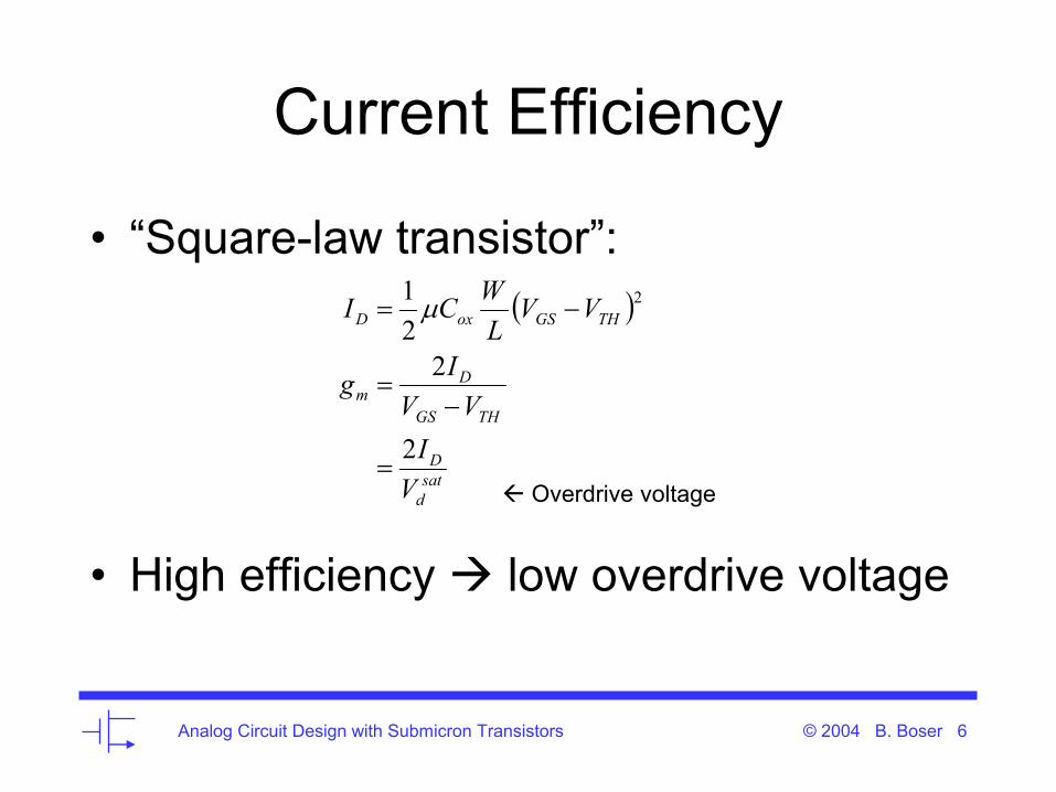
Current Efficiency
• “Square-law transistor”:
• High efficiency low overdrive voltage
( )
satd
D
THGS
Dm
THGSoxD
VI
VVIg
VVLWCI
2
221 2
=
−=
−= µ
Overdrive voltage

Analog Circuit Design with Submicron Transistors © 2004 B. Boser 7
Current Efficiency gm/ID• High efficiency is good
for low power
• Higher gm/ID at low VGS
• Approaches BJT for VGS < VTH
gm/IC = 1/Vt ~ 40 V-1
• Weak dependence on transistor type and process

Analog Circuit Design with Submicron Transistors © 2004 B. Boser 8
Transit Frequency ωT
• Unity current-gain bandwidth
model) law-(square 2LV
CCg
satd
gdgs
mT
µ
ω
≈
+=

Analog Circuit Design with Submicron Transistors © 2004 B. Boser 9
Efficiency gm/ID versus fT
Speed-Efficiency Tradeoff
NMOS faster than PMOS
Analog Circuit Design with Submicron Transistors © 2004 B. Boser 10
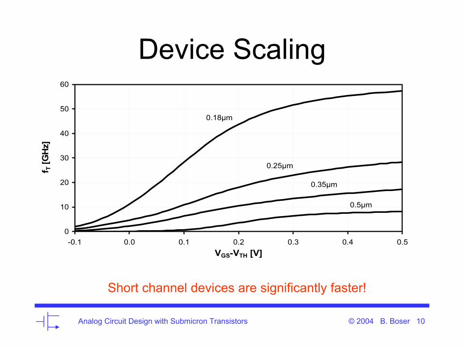
Device Scaling
0
10
20
30
40
50
60
-0.1 0.0 0.1 0.2 0.3 0.4 0.5VGS-VTH [V]
f T [G
Hz]
0.18µm
0.25µm
0.35µm
0.5µm
Short channel devices are significantly faster!
Analog Circuit Design with Submicron Transistors © 2004 B. Boser 11
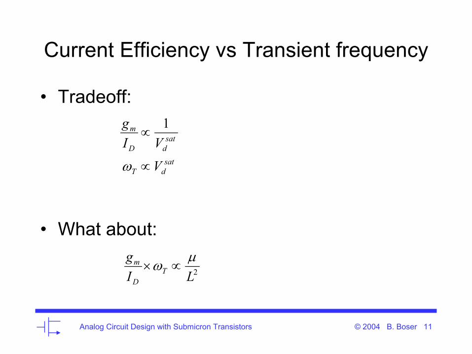
Current Efficiency vs Transient frequency
• Tradeoff:
• What about:
satdT
satdD
m
V
VIg
∝
∝
ω
1
2LIg
TD
m µω ∝×
Analog Circuit Design with Submicron Transistors © 2004 B. Boser 12
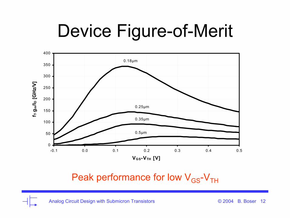
Device Figure-of-Merit
Peak performance for low VGS-VTH
0
50
100
150
200
250
300
350
400
-0.1 0.0 0.1 0.2 0.3 0.4 0.5
VGS-VTH [V]
f T⋅g
m/I D
[GH
z/V]
0.18µm
0.25µm
0.35µm
0.5µm
Analog Circuit Design with Submicron Transistors © 2004 B. Boser 13
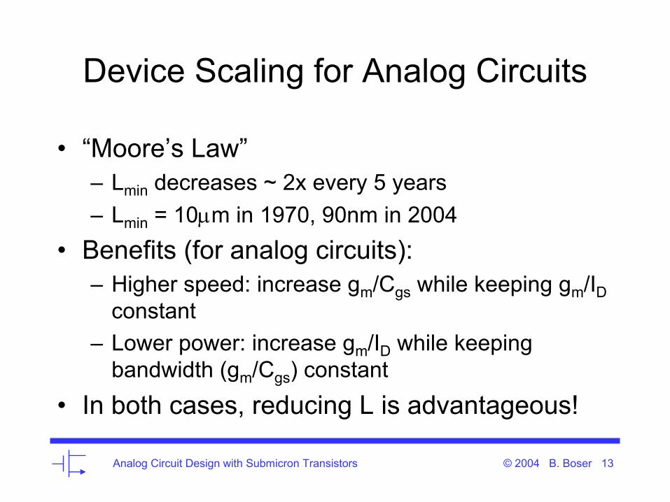
Device Scaling for Analog Circuits
• “Moore’s Law”– Lmin decreases ~ 2x every 5 years– Lmin = 10µm in 1970, 90nm in 2004
• Benefits (for analog circuits):– Higher speed: increase gm/Cgs while keeping gm/ID
constant– Lower power: increase gm/ID while keeping
bandwidth (gm/Cgs) constant• In both cases, reducing L is advantageous!
Analog Circuit Design with Submicron Transistors © 2004 B. Boser 14
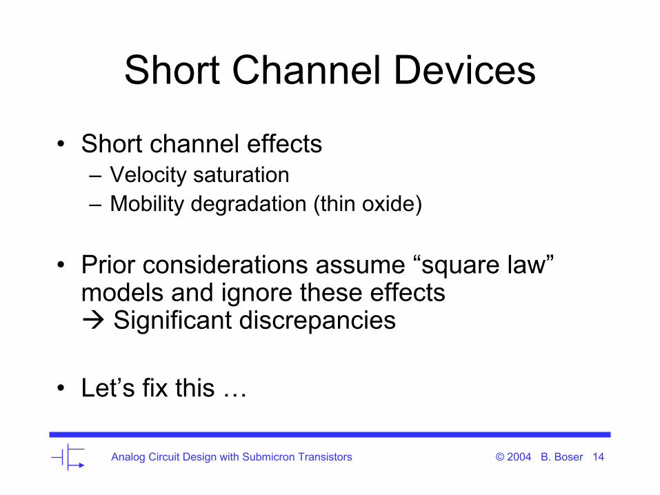
Short Channel Devices
• Short channel effects– Velocity saturation– Mobility degradation (thin oxide)
• Prior considerations assume “square law”models and ignore these effects
Significant discrepancies
• Let’s fix this …
Analog Circuit Design with Submicron Transistors © 2004 B. Boser 15
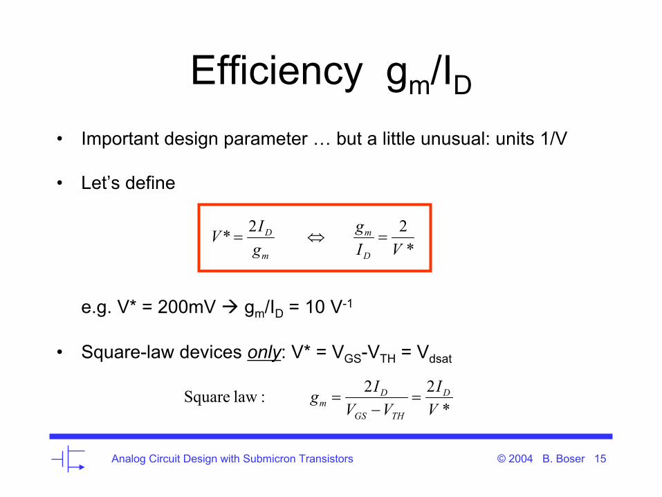
Efficiency gm/ID• Important design parameter … but a little unusual: units 1/V
• Let’s define
e.g. V* = 200mV gm/ID = 10 V-1
• Square-law devices only: V* = VGS-VTH = Vdsat
*22 :law SquareVI
VVIg D
THGS
Dm =
−=
*2 2*VI
ggIV
D
m
m
D =⇔=
Analog Circuit Design with Submicron Transistors © 2004 B. Boser 16
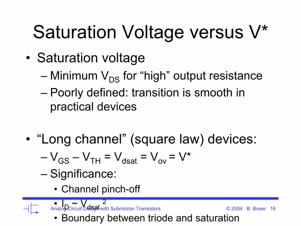
Saturation Voltage versus V*• Saturation voltage
– Minimum VDS for “high” output resistance– Poorly defined: transition is smooth in
practical devices
• “Long channel” (square law) devices:– VGS – VTH = Vdsat = Vov = V*– Significance:
• Channel pinch-off• ID ~ Vdsat
2
• Boundary between triode and saturation
Analog Circuit Design with Submicron Transistors © 2004 B. Boser 17
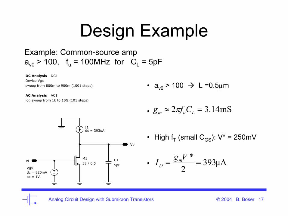
Design ExampleExample: Common-source amp av0 > 100, fu = 100MHz for CL = 5pF
• av0 > 100 L =0.5µm
•
• High fT (small CGS): V* = 250mV
•
mS14.32 =≈ Lum Cfg π
µA3932
*==
VgI mD
M138 / 0.5 Vgs
dc = 820mVac = 1V
I1dc = 393uA
Vi
Vo
DC Analysis
sweep from 800m to 900m (1001 steps)Device Vgs
DC1
AC Analysislog sweep from 1k to 10G (101 steps)
AC1
C15pF

Analog Circuit Design with Submicron Transistors © 2004 B. Boser 18
Device Sizing• Pick L 0.5µm• Pick V* 250mV• Determine gm 3.14mS
• ID = 0.5 gm V* 393µA
• W from graph (generate with SPICE)
W = 10µm (393µA /103µA)= 38µm
• Create such graphs for several device length’ for design reference
NMOSW / L = 10 / 0.5
Analog Circuit Design with Submicron Transistors © 2004 B. Boser 19
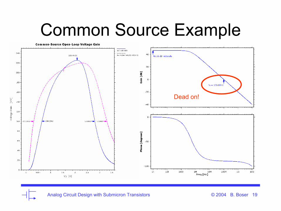
Common Source Example
Dead on!

Analog Circuit Design with Submicron Transistors © 2004 B. Boser 20
Device Sizing ChartW = 10µm for all devicesVDS = VGS VSB = 0V
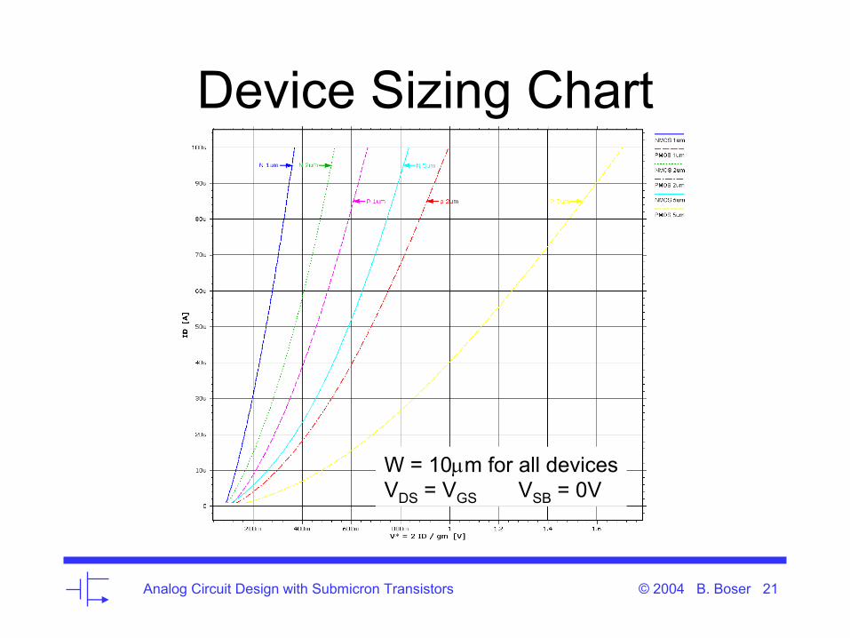
Analog Circuit Design with Submicron Transistors © 2004 B. Boser 21
Device Sizing Chart
W = 10µm for all devicesVDS = VGS VSB = 0V
Analog Circuit Design with Submicron Transistors © 2004 B. Boser 22
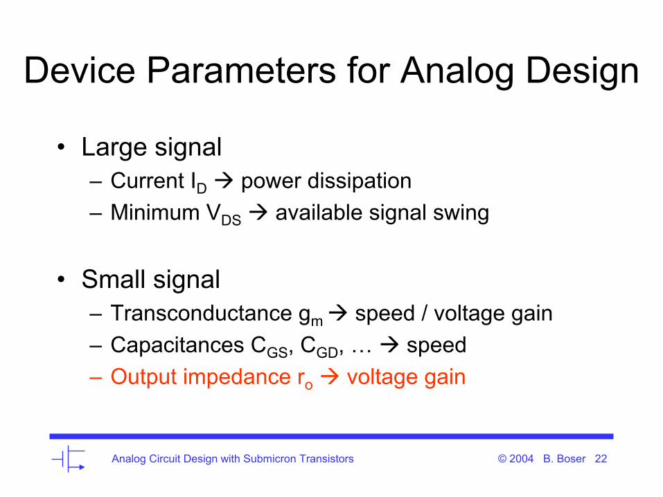
Device Parameters for Analog Design
• Large signal– Current ID power dissipation– Minimum VDS available signal swing
• Small signal– Transconductance gm speed / voltage gain– Capacitances CGS, CGD, … speed– Output impedance ro voltage gain
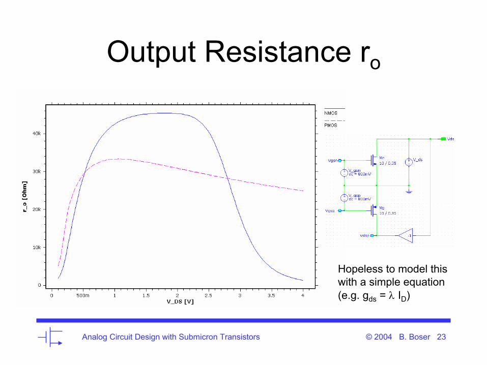
Analog Circuit Design with Submicron Transistors © 2004 B. Boser 23
Output Resistance ro
Hopeless to model this with a simple equation(e.g. gds = λ ID)
Analog Circuit Design with Submicron Transistors © 2004 B. Boser 24
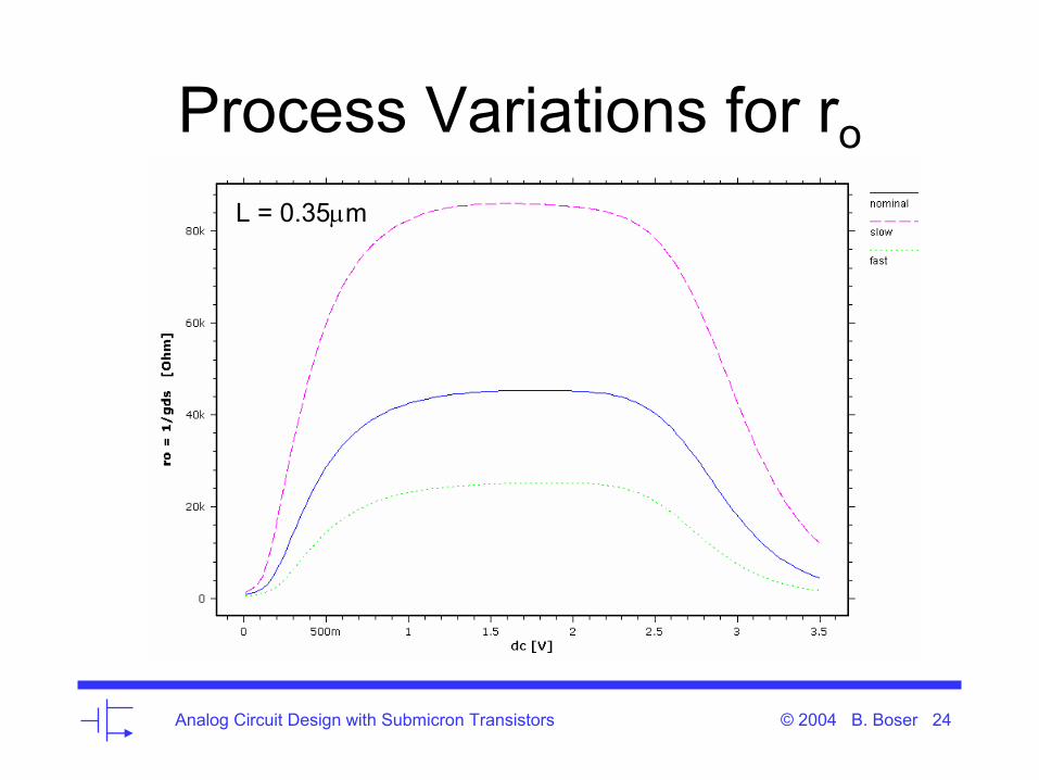
Process Variations for ro
L = 0.35µm
Analog Circuit Design with Submicron Transistors © 2004 B. Boser 25
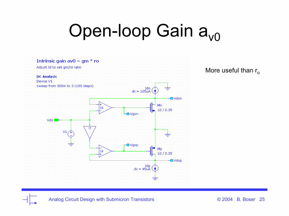
Open-loop Gain av0
More useful than ro
Analog Circuit Design with Submicron Transistors © 2004 B. Boser 26
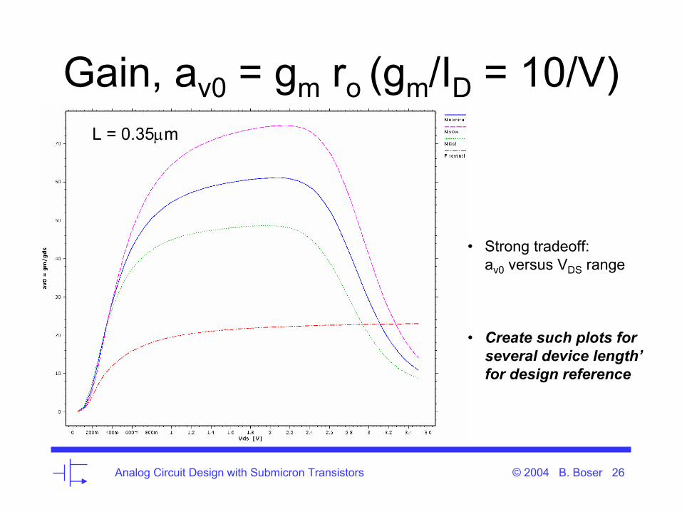
Gain, av0 = gm ro (gm/ID = 10/V)
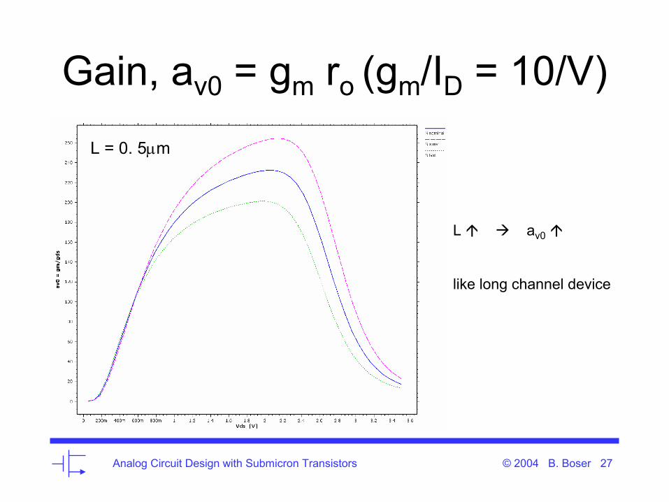
• Strong tradeoff:av0 versus VDS range
• Create such plots for several device length’for design reference
L = 0.35µm
Analog Circuit Design with Submicron Transistors © 2004 B. Boser 27
Gain, av0 = gm ro (gm/ID = 10/V)
L = 0. 5µm
L av0
like long channel device
Analog Circuit Design with Submicron Transistors © 2004 B. Boser 28
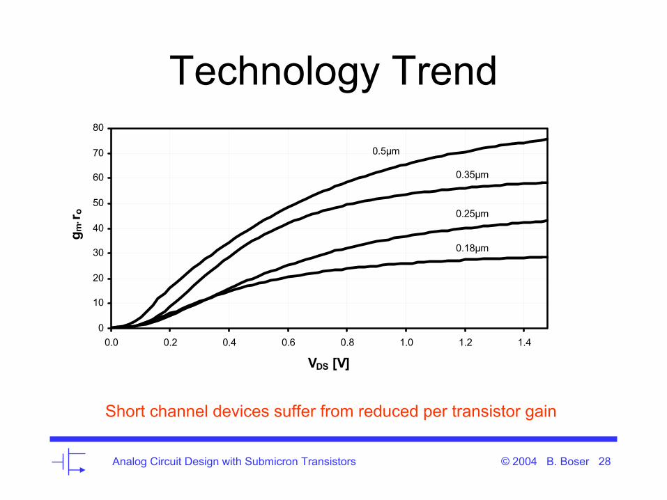
Technology Trend
0
10
20
30
40
50
60
70
80
0.0 0.2 0.4 0.6 0.8 1.0 1.2 1.4
VDS [V]
g m⋅r o
0.18µm
0.25µm
0.35µm
0.5µm
Short channel devices suffer from reduced per transistor gain

Analog Circuit Design with Submicron Transistors © 2004 B. Boser 29
Transistor Gain Detail
For practical VDS the effect the “short-channel” gain penalty is less severe(remember: worst case VDS is what matters!)
0
5
10
15
20
25
30
35
40
45
0.0 0.1 0.2 0.3 0.4
VDS [V]
gm⋅r
o
0.18µm
0.25µm
0.35µm
0.5µm
Analog Circuit Design with Submicron Transistors © 2004 B. Boser 30
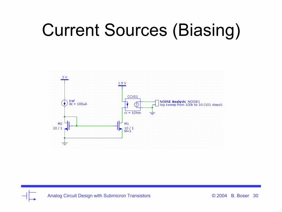
Current Sources (Biasing)
Analog Circuit Design with Submicron Transistors © 2004 B. Boser 31
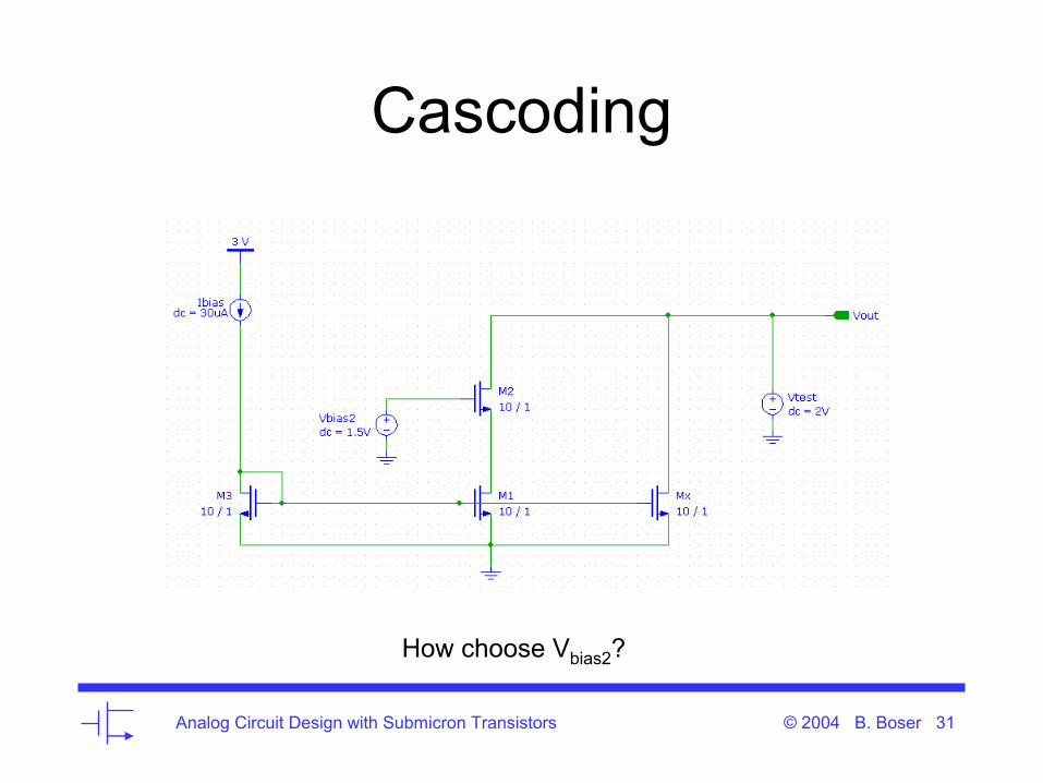
Cascoding
How choose Vbias2?

Analog Circuit Design with Submicron Transistors © 2004 B. Boser 32
Output Resistance
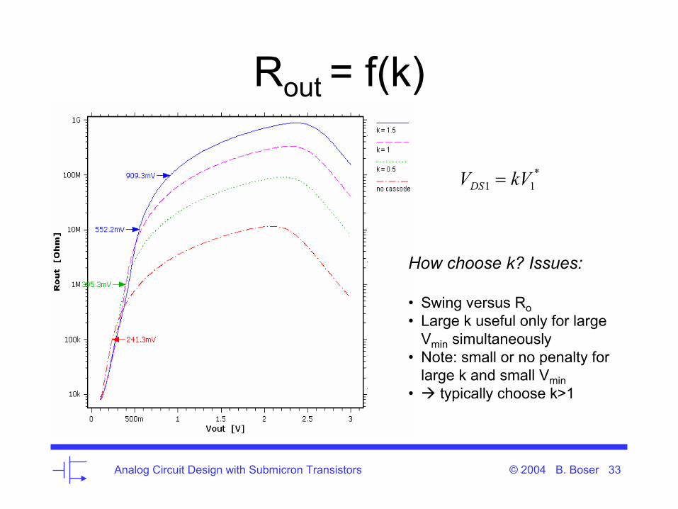
Analog Circuit Design with Submicron Transistors © 2004 B. Boser 33
Rout = f(k)
*11 kVVDS =
How choose k? Issues:
• Swing versus Ro• Large k useful only for large
Vmin simultaneously• Note: small or no penalty for
large k and small Vmin• typically choose k>1
Analog Circuit Design with Submicron Transistors © 2004 B. Boser 34
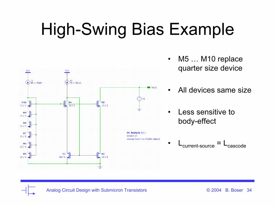
High-Swing Bias Example• M5 … M10 replace
quarter size device
• All devices same size
• Less sensitive to body-effect
• Lcurrent-source = Lcascode
Analog Circuit Design with Submicron Transistors © 2004 B. Boser 35
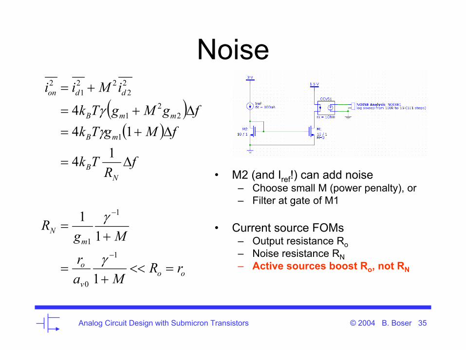
Noise
• M2 (and Iref!) can add noise– Choose small M (power penalty), or– Filter at gate of M1
• Current source FOMs– Output resistance Ro– Noise resistance RN– Active sources boost Ro, not RN
( )( )
oov
o
mN
NB
mB
mmB
ddon
rRMa
r
MgR
fR
Tk
fMgTkfgMgTk
iMii
=<<+
=
+=
∆=
∆+=∆+=
+=
−
−
1
11
14
144
1
0
1
1
1
22
1
22
221
2
γ
γ
γγ
Analog Circuit Design with Submicron Transistors © 2004 B. Boser 36
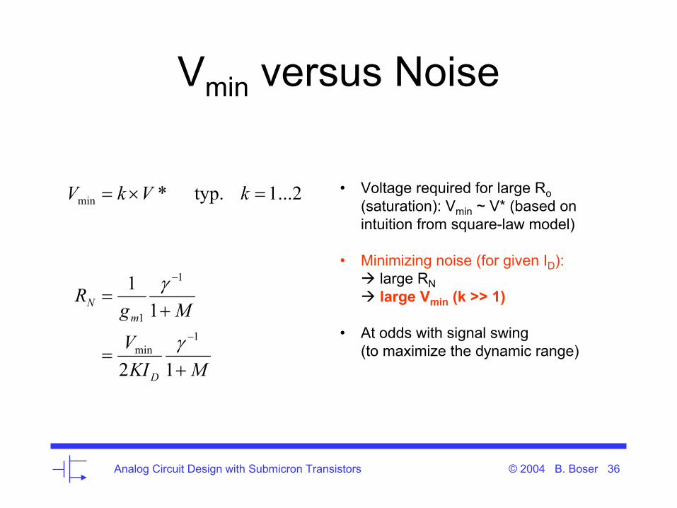
Vmin versus Noise
MKIV
MgR
kVkV
D
mN
+=
+=
=×=
−
−
12
11
2...1 typ.*
1min
1
1
min
γ
γ
• Voltage required for large Ro(saturation): Vmin ~ V* (based on intuition from square-law model)
• Minimizing noise (for given ID):large RNlarge Vmin (k >> 1)
• At odds with signal swing(to maximize the dynamic range)

Analog Circuit Design with Submicron Transistors © 2004 B. Boser 37
Bipolar’s, GaAs, …
• BJT and RE contribute noise• Increasing RE lowers overall noise• BJT and MOS exhibit essentially
same noise / Vmin tradeoff• Lowest possible noise source is a
resistor (and large Vmin, VDD)
Q1Q2
RERE
io
Iref
Cbig
fRgRgi
Rgii
Em
EmRn
Emcnon ∆
++
+=
44344214434421ER
22
BJT
222
111
0 a) =EmRg
1 b) >>EmRg
fTgki mBon ∆= 22
fR
TkiE
Bon ∆=142
CC
t
mN I
IV
gR by set 22
==
min
minmin
VVV
IVRR
satce
CEN
−==
KIVRD
MOSN 2 compare
1min
,
−
=γ
( )02 =bi

Analog Circuit Design with Submicron Transistors © 2004 B. Boser 38
Small Signal Design Summary• Determine gm (from design objectives)
• Pick L– Short channel high fT– Long channel high ro, av0
• Pick V* = 2ID/gm– Small V* large signal swing– High V* high fT– Dynamic range: Psig ~ 1/V*, Pnoise ~ V*
• Determine ID (from gm and V*)
• Determine W (SPICE / plot)
• Accurate for short channel devices key for design

Analog Circuit Design with Submicron Transistors © 2004 B. Boser 39
Device Parameter Summary
• Obtain from L, ID• Self loading (CGS, CDB, …)
W
• Cutoff frequency, fT phase margin• Intrinsic transistor gain (av0)
L
• Current efficiency, gm/ID• Power dissipation (ID)• Speed (gm)• Cutoff frequency, fT phase margin• Headroom, VDS,min
V*
Circuit ImplicationsDevice Parameter
Top Related