


Languages
Pages
Legal


AN INTERFACE BETWEEN THE SAI-42 CORRELATIONAND PROBABILITY ANALYZER AND THE ASR-33
TELETYPEWRITER SET
Arthur Hugh Col 1 ier
i


NAVAL POSTGRADUATE SCHOOL
Monterey, California
THESISAN INTERFACE BETWEEN THE SAI-42CORRELATION AND PROBABILITYANALYZER AND THE ASR-33TELETYPEWRITER SET
by
Arthur Hugh Collier
Th 5Sis Advisor: Louis V. SchmidtMarch 1972
Approved loK public. h.oJLexLi>Q.; cLUtnAhiitioYi antunltud.


An Interface Between the SAI-42 Correlation
and Probability Analyzer and the
ASR-33 Teletypewriter Set
by
Arthur Hugh Collier
Lieutenant, United States NavyB.S., United States Naval Academy, 1964
Submitted in partial fullfillment of the
requirements for the degree of
MASTER OF SCIENCE IN AERONAUTICAL ENGINEERING
from the
NAVAL POSTGRADUATE SCHOOLMarch 1972


ABSTRACT
The purpose of the interface device is to make possible the
collection or storage of data from a laboratory instrument in punched
paper tape format, suitable for subsequent transmission to a digital
computer.
Important aspects of the interface design are presented and
problems encountered in this design are discussed. The micrologic
digital design is presented and its operation discussed.


TABLE OF CONTENTS
I. INTRODUCTION 7
II. NATURE OF THE PROBLEM 10
A. DESCRIPTION OF THE SAI-42 CORRELATIONAND PROBABILITY ANALYZER 10
1. Description of BCD Code 10
B. DESCRIPTION OF THE ASR -33
TELETYPEWRITER SET 13
1. Description of the ASCII Code 14
C. DESCRIPTION OF THE LIVER MORE DATA SYSTEMS,INC. ACOUSTIC COUPLER MODEL B 15
D. ONLINE DATA AQUISITION UNDER OS/360 15
III. INTEGRATED CIRCUIT SUMMARY 17
IV. DEFINITION OF THE DESIGN 20
V. DESIGN DEVELOPMENT 23
VI. THE PROPOSED DESIGN 25
A. DESCRIPTION OF THE CONVERTER 25
B. DESCRIPTION OF THE CONTROLLER 28
C. MODIFICATION OF THE SAI-42 33
VII. SUMMARY 34
REFERENCES 45
INITIAL DISTRIBUTION LIST 46
FORM DD 1437 47


LIST OF TABLES
I. SAI -42 OUTPUT CODING 11
II. BINARY AND EQUIVALENT DECIMAL NUMBERS 12


LIST OF FIGURES
1 Teletypewriter and External Equipment 35
2a ASCII Code Character Arrangement 36
2b Current Waveform for Letter "U" 36
3 Logic Elements 37
4 Data Format on Teletype Unit 38
5 Converter and Controller Block Diagram 39
6 Required Teletype Code 40
7 Converter Section 41
8 Controller Section 42
9 Transmission Timing Sequence 43
10 Entire Design Schematic 44


ACKNOWLEDGMENTS
The author wishes to express indebtedness to the following
persons at the U.S. Naval Postgraduate School:
Dr. Louis V. Schmidt, Professor of Aeronautics, for the thesis
topic and for guidance during the thesis preparation.
Dr. V. Michael Powers, Assistant Professor of Electrical
Engineering, for technical advice and help in the design of the inter-
face.


I. INTRODUCTION
The rapid processing of data to allow an increased scope of
experimental analysis has been a known feature of many laboratories
for a number of years. The need for updating experimental facilities
at the Naval Postgraduate School in order to improve data acquisition
systems follows upon the heavy emphasis placed upon the student and
faculty to use large in-house computer facilities for problem solving.
Data reduction requires several value judgments to be made. A
distinction must be made between slow, medium, and fast data acqui-
sition rates, a reasonable definition (relative to a four-digit-plus-sign
number) being:
slow rate . . . recorded at speeds up to one number per second;
medium rate . . . recorded at speeds from one to 100 numbersper second;
fast rate . . . recorded at speeds above 100 numbers per
second.
Different techniques are feasible for recording and processing of data
at each rate.
At the present time, an immediate need exists for data handling
at a slow rate for laboratory experiments in the Department of Aero-
nautics. The following are examples:
a. wind-tunnel balance readings of model attitude, loads and moments,
b. pressure readings either from a single transducer multiplexed to

a series of pressure sources via a scani-valve or from a
multiple array of transducers multiplexed directly to the data
acquisition system,
c. thermocouple readings,
d. strain gage measurements on experimental stress problems,
and
e. alternate recordings of frequency and acceleration amplitude at
several model stations of a dynamic model for engineering
mechanics problems.
The Aeronautics laboratories are confronted with a need to
process time-varying analog signals, such as hot-wire measurements
of turbulent flow fields, oscillating pressures on a moving aeroelastic
wind-tunnel model, and motion and accelerations of a dynamic model
in the engineering mechanics environment. Although a capability
exists to record these types of data on magnetic tape in analog form,
the subsequent digitizing process for analysis purposes is inadequate.
The initial problem posed was to interface a signal correlator
with a punched paper -tape output device. The correlator makes
possible the processing of time -varying analog input data, such as hot-
wire signals into an output form, either auto- or cross-correlation,
accessible as digitized signals for slow-rate acquisition. Once the
output was obtained in computer compatible form (punched paper tape),
the next problem was to conveniently input the data into a computer for
processing. It is the purpose of this thesis to address both of the
8


above problems. As will be shown, the development of interface
equipment between a digital source and an output device requires the
design of logic circuitry using compact integrated circuit (IC) logic
devices. The latter problem of data input to the computer was par-
tially solved using the large central computer in conjunction with an
acoustic coupler from the paper tape reader. However, there is a
possibility for the future that low cost (approx. $10, 000) mini-
computers would be available to the laboratory for direct, on-line
data reduction.

II. NATURE OF THE PROBLEM
A. DESCRIPTION OF THE SAI-42 CORRELATION ANDPROBABILITY ANALYZER
The SAI-42 correlation and probability analyzer is a high-speed
processing instrument which provides on-line, real-time computation
in three primary operating modes: correlation (auto and cross),
enhancement (or signal recovery) and probability (density and distri-
bution). In all modes, 100 analysis points are computed and stored
in memory bins labeled 0-99.
Input to the SAI-42 is provided through two identical, independent
channels (A and B). Several output modes are available. These include
Fast (for use with an oscilloscope), Spectrum (for compatability with
the SAI-51 Spectrum Analyzer), Slow (for use with chart recorders) and
Single (for use with X-Y plotters). The SAI-42 was purchased with an
optional BCD output capability (option 42040) which makes available
digital outputs at a multi-pin rear panel connector. See Table I for the
format. In BCD, the function output is represented by three parallel
BCD digits and a sign bit, while two parallel BCD digits represent the
bin number. Two synchronizing pulses are also supplied.
1. Description of BCD Code
In electronic circuits, such as those used in a digital com-
puter, the fewer the unambiguously distinguishable states, the greater
tha reliability and simplicity of the circuit. The minimum number of
10


states a circuit can have and still be useful is two. Included in the
advantages of two-state circuits over circuits with more than two
states are that their output levels are easy to distinguish, arithmetic
operations are simple, and many components such as switches, relays
and diodes, which only have two states (ON or OFF), can be used as
active devices. A two-state circuit is called a "binary circuit."
Table I. SAI-42 Output Coding
Signal
OutputConn Pin Weight
Function
Function
Function
VWXY
Za
b
c
d
e
AABB
(2U
(21
(22
(23
(2°
(2*
(22
(23
(2°
(2l
(22
(2 3
Unit's Place
Ten's Place
Hundred'sPlace
Sign
Bin Number
Bin Number
Busy Out
SYNC DO
f
h
3
k
1
mn
P
r
t
sign
(2U
)
(21
)
(22
)
(23
)
(2°)
(21
)
(22
)
(23
)
Unit's Place
Ten's Place
11


If each binary circuit were to represent a digit, then by analogy
with the base- 10 number system, each digit will represent the coeffi-
cient of some power of 2. Counting in the base 2 (binary) system goes
as follows: 0, 1, 10, 11, 100, 101, etc. The number 1001 is lx2 3 +
0x2^ + 0x2 + 1x2^ which is equivalent to 9 in the decimal system.
Four binary circuits (A, B, C, and D), of which the outputs are either
or 1, can be used to represent all the numbers between 0000 and 1111
(0-15 in decimal) as shown in Table II.
Binary Numbers
X2 3 X2 2 X2 1 X2° Equivalent
D C B A Decimal Numbers
1 1
1 2
1 1 3
1 4
1 1 5
1 1 6
1 1 1 7
8
1 9
1 10
1 1 11
1 12
1 1 13
1 1 14
1 1 1 15
Table II. Binary and Equivalent Decimal Numbers
The conversion of a number from the binary system to the more
familiar decimal system is a fairly simple process for small numbers,
but for larger numbers the process becomes unwieldy and time-
12


consuming. "Binary-coded decimal" numbers are often used when
dealing with large numbers which will eventually be converted to
decimal presentation. Four circuits are used in combination to rep-
resent the numbers 0000 to 1001 (See Table II). This ordered set of
four binaries then represents one digit of a decimal number. Another
set of four binaries is used to represent the next digit and so on. For
example, from Table II, the binary-coded decimal number 0011, 1000,
0110, is the number 386 in decimal notation.
B. DESCRIPTION OF THE ASR-33 TELETYPEWRITER SET
The ASR-33 (Automatic Send-Receive) Teletypewriter Set is an
electromechanical apparatus that provides terminal facilities for
exchanging recorded communication via appropriate transmission
facilities, including telegraph lines, telephone networks, and radio
channels. Transmission and reception is effected by the use of the
8-bit American Standard Code for Information Interchange (ASCII) and
a start-stop signaling code which is carried by transmission facilities.
The Teletypewriter Set will operate at speeds up to 600 characters per
minute.
The simple three line circuit shown in Figure 1 on page 35, illus-
trates the transmission and reception of code. Making and breaking the
contact between the common and receive lines at the appropriate rate
i.e., 110 bits per second (bps), using the appropriate code (ASCII), plus
start and stop pulses causes a coded character either to be printed
(typed) or to be both printed and punched in paper tape. Similarly,
13


either typing or reading paper tape will cause the ASCII code repre-
senting a character to be sent.
1. Description of the ASCII Code
The American Standard Code for Information Interchange
(ASCII) accommodated by the typing unit is illustrated in Figure 2a on
page 36 • Since it has eight intelligence elements and its stop and start
elements comprise three units of time, the code is an 8 -level code with
an 11 -unit transmission pattern. However, at present, it utilizes only
the first seven intelligence elements, the eighth being used to provide
a marking element. Thus it has 2 , or 128 available permutations. Of
these combinations, 64 are assigned to printing characters. The rest
either are devoted to control (nonprinting) characters or are unassigned.
The character arrangement for the ASCII code is shown on
the chart in Figure 2a. The black circles represent marking elements,
the blank squares spacing elements. The main block gives the arrange-
ments of elements 1 through 5. The four smaller blocks at the right
give the arrangements of elements 6 and 7 for the four rows of charac-
ters as indicated by the arrows. For example, the eight bit ASCII code
representing the letter "U" is 10101011. The transmission pattern
required to send this character, including start and stop pulses, is
01010101111.
The waveform of the current through the transmission lines
necessary to receive and print or print and punch the letter "U" is
shown in the bottom of Figure 2b. The mark level indicates current
14


flow, or a binary 0. The frequency of transmission is 110 bps which
corresponds to a time unit of 9. 09 msec per pulse.
C. DESCRIPTION OF THE LIVER MORE DATA SYSTEMS, INC.ACOUSTIC COUPLER MODEL B
The Livermore Data Systems, Inc. acoustic coupler is designed
to accept serial binary digital data, translate the data into audible tones,
and transmit the tones via either leased lines or the dial-up telephone
network to another acoustic coupler or data-set at the remote site. The
transmitted tones are decoded at the receiving end and the digital data
reconstructed for use by another terminal or computer.
These acoustic couplers are designed to interface with terminal
equipment that meets the electrical interface requirements as defined
in E1A Standard RS-2328. In addition, circuitry is included which
allows operation with a Teletype terminal wired for 20-milliampere
full-duplex operation.
D. ONLINE DATA -ACQUISITION UNDER OS/360
Data from experimental measurements are frequently recorded
on punched paper tape for subsequent processing on a digital computer
system at the Naval Postgraduate School. This has been recognized
and an online data-aquisition capability under IBM OS/360 has been
developed. See Ref. 3 for more information on this data-aquisition
capability. It is now possible for a user while using a teletype termi-
nal which is connected to the OS/360 System to read punched paper tape
directly into the IBM 360 Computer. The following options are available:
15

1. To read and store paper tape data (raw data) in the OS/360
System for later processing.
2. To convert the paper tape data to IBM/360 code, format
the data as specified by the user, and then either store or
punch out the formatted data. The data are then in a form
ready to be analyzed by a user's program.
16


III. INTEGRATED CIRCUIT SUMMARY
There are many types of integrated circuits available- -the most
popular being Transistor-Transistor Logic (TTL), Medium Scale Inte-
gration (MSI), Resistor -Transistor Logic (RTL), and Diode-Transistor
Logic (DTL). Due to the close proximity of a distributor and the avail-
ability of technical advice, Fairchild Semiconductor integrated circuits
were used in the design.
Fairchild groups the above mentioned types into their Compatible
Current Sinking Logic (CCSL) family. This refers to all standard Fair-
child logic circuits that operate by sinking current into the outputs in
the low state and supplying leakage current from the output in the high
state. Current sinking logic is one of three forms of logic, the other
two being current sourcing logic and current mode logic.
All circuits that make up CCSL have common power supply volt-
ages and compatible logic levels at the input and output. Since all the
input and output levels are compatible these circuits are a set of inte-
grated logic building blocks which are well suited for this design.
The two logic levels in all elements of this device are the posi-
tive level "l, " and the negative level "0. " The voltage level corres-
ponding to a "1" ranges from 2.4 to 7.0 volts and the voltage level
corresponding to a "0" is -0.5 to 0.4 volts.
The basic elements used in the construction of the interface are
two input NAND gates, three input NAND gates, inverters, multiplexers,
17


J-K flip flops, shift registers, and binary counters. The operation of
these elements is briefly described in the following paragraphs. (See
Ref. 4 for more details on operational use).
1. Inverter
The inverter is used to complement the incoming signal or
pulse. If the input were at a logic level of "1, " the output
of the inverter would be at a logic level of "0, " and vice-
versa.
2. NAND Gate
The purpose of a nand-gate is to logically combine two or
more inputs. The output of the gate is always "l" unless
all inputs to the gate are "l" and only then is the output "0"
as shown in the truth table of Figure 3.
3. Multiplexers
The purpose of a multiplexer is to logically select one bit
of data from each of several sources. The bit of data
logically selected is controlled by the state of the control
inputs. These inputs represent a binary number from to
n, the number of available data bits.
4. Shift Register
The shift register may be used in serial-serial, shift left,
shift right, serial-parallel, parallel-serial, and parallel-
parallel data transfers.
18


5. Binary Counters
The binary counter is, in most cases, a synchronous four-
bit binary counter. It is able to count in binary from 0000
to 1111, each increment being caused by a clock pulse. It
is capable of being reset asynchronously to 0000.
6. J-K Flip-Flop
The J-K Flip-Flop is a one-bit memory which can be used
in a variety of applications. In addition to the J-K function,
it can be wired to the functions of the "Triggered" (T),
"clocked T, " and the simple set-rest flip-flops. In this
design it was used as a set-reset flip-flop. This function
is shown in Figure 3.
By combining inverters andNAND-gatesit is possible to perform
other functions. These functions include and-gates and or -gates and
are constructed as shown in Figure 3.
19


IV. DEFINITION OF THE DESIGN
The availability of the parallel BCD output from the SAI-42 and
the ability of the ASR-33 to receive ASCII coded information for trans-
mission and recording made an integration of the two capabilities highly
desirable. Several problems became apparent during the consideration
of the design necessary to interface these two units.
The primary problem was the conversion of the parallel BCD out-
put from the SAI-42 into serially flowing ASCII coded signals for the
ASR-33. Six characters of information, i.e., two decimal digits for
the memory bin number, three digits for the function value, and a sign
bit, were available in BCD form, concurrently from the SAI-42 for a
limited amount of time, 500 msec per memory bin. It would be neces-
sary to cycle through each of these six characters of information and
convert their BCD representations into their corresponding ASCII code
and serially transmit the ASCII code into the ASR-33 in the 500 msec
available. Additionally each character transmitted to the ASR-33 was
to be punched on paper tape and printed for an echo check. The ASR-
33 is capable of printing 72 characters across the page so it was
necessary to plan for the transmission of carriage return and line
feed characters after the line was full. A further problem became
apparent in the necessity to include an "X-OFF" control character
periodically. This character is required by the IBM-360 due to the
limited record length it can receive at one time. When the punched
20


tape is transmitted to the IBM-360 from the ASR-33, via the audio
coupler, the appearance of an "X-OFF" character causes the ASR-33
to pause until the IBM-360 signals it via an "X-ON" character on the
return line to continue sending data. This pause allows the IBM-360
to service other terminals on its time sharing schedule.
The ASR-33 receives ASCII code serially at the rate of 110 bps.
The eight bit ASCII code plus three bits for start and stop pulses com-
prise 11 bits, or time units, per character. At the 110 bps trans-
mission rate this allows 10 characters to be received by the ASR-33
per second. This created a problem in that there were a minimum of
six characters necessary to obtain all the information from each
memory bin and periodically carriage return, line feed and "X-OFF"
control characters are required to be transmitted to the ASR-33 in the
500 msec that the BCD information is available from the SAI-42. A
maximum of nine characters, each requiring 100 msec, could not be
transmitted in 500 msec therefore requiring a revision.
The solution to these problems included two basic design con-
siderations. One part of the solution was the modification of the logic
circuitry of the SAI-42 to allow each memory bin to be available twice
as long, i.e., 1 sec. vice 500 msec. The second part of the solution
was to format the data input in such a manner that it would not be
necessary to print and punch the memory bin number associated with
the data being received. The format selected is shown in Figure 4.
It was decided that there would be ten function values on each line with
21

sign information and a space between each value. These would corres-
pond to memory bins 0-9, the second line to memory bins 10-19, . . .
etc., through memory bins 90-99. After each line, carriage return,
line feed and "X-OFF" control characters would be transmitted to the
ASR-33. It would have been possible to transmit the six characters,
corresponding to memory bin number and function value, a space
between them, plus carriage return, line feed and "X-OFF" control
characters as required, in the 1 sec. available, but the possibility of
losing synchronization would have been too great. It was decided that
the deletion of the bin numbers would present no problem in the manual
interpretation of the output and would require less format control from
the IBM-360 program accepting the data.
22


V. DESIGN DEVELOPMENT
After the basic design requirements were identified it became
necessary to formulate more specifically the manner in which these
requirements would be implemented. The overall design was broken
into two basic parts or modules: The converter for the transforming
of parallel inputs into ASCII coded serial outputs and the controller
for the sequencing and timing. This is shown in Figure 5. The parts
were to be made up of solid state integrated circuits.
The various codes necessary to generate the required characters
in ASCII code were tabulated as shown in Figure 6. Also, as can be
seen from Figure 6, each character code has start and stop bits plus
bits 7 and 8 of the ASCII code in common. Bits 1 through 6 of the ASCII
code vary with the character being transmitted.
It was decided that the converter would consist of three four -bit
shift registers and a set of six multiplexers. The outputs of the multi-
plexers would be moved in parallel into the shift registers, to construct
the desired code, and shifted out serially to the ASR-33. The controller
would handle various timing problems and control the switching of the
multiplexers.
The multiplexers, being logically switched by the controller,
would move the proper code into the shift registers for serial output
to the ASR-33. It was noted that bits 1-4 of the ASCII code for the
decimal numbers 0-9 was exactly the same as the BCD representation
23


of these numbers. (See Table II and Figure 2a). It was also noted
that the multiplexers could receive the function values in BCD form,
directly from the SAI-42, and channel them into the shift registers.
In switching the multiplexers, the controller would determine
the sequencing of characters, logically causing line feed, carriage
return and "X-OFF" characters to be transmitted to the ASR-33 after
ten sets, or words, of space, sign, and function value had been trans-
mitted. Additionally the controller would convert bit-clock pulses into
character -clock pulses and character -clock pulses into word-clock
pulses. Finally, the controller would not initiate any of the above
mentioned events until signaled by the SAI-42 that it had completed
its functions and was ready to transmit data. A subpart of this control
function would be to inhibit all events after the transmission of each
set of characters until the SAI-42 switched to the next memory bin.
This timing function became necessary when it was decided to double
the time, from 500 msec to 1 sec, that the SAI-42 displayed each
memory bin.
24


VI. THE PROPOSED DESIGN
The design process continued by transforming the design require-
ments into the necessary logic schematics. As the logic of the proposed
design progressed it was breadboarded using the actual integrated cir-
cuits. The availability of breadboard facilities greatly increased the
progress of the design as it pointed out errors in timing, gating, etc. ,
not previously considered. Extensive use was made of a Heathkit Model
EU-801A logic trainer and a Perfection Electronic Product Corporation
Logilab Mod I. The Heathkit logic trainer provided a variable bit clock,
logic level indicator lights, a power source, manual switches, and a
limited capacity for patching special purpose integrated circuit chips.
The Logilab provided extensive integrated circuit patching capabilities
along with low contact-bounce toggle and push-button switches.
A. DESCRIPTION OF THE CONVERTER
The final design is presented in Figures 7 and 8. The converter
module (Figure 7) is made up of six eight-input multiplexers and three
four-bit shift registers. The output of the multiplexers is determined
by the value of the number represented in binary by the three switching
inputs labeled a, b, and c. These three inputs, or bits, can take in
binary values ranging from 000 to 1 1 1 which are equivalent to the
values to 7 in decimal. The inputs labeled through 7 are fed through
tlTe multiplexer according to the value through 7, represented in binary
25 •


by inputs a, b, and c. The output of each multiplexer is then fed into
the correct position of the shift-registers. As can be seen in Figure
6, the eleven bit code necessary to generate a character on the ASR-
33 differs from character to character.
The first character transmitted is always a space. In order to
have the proper code, the switch inputs a, b, and c to the multiplexers
must be 000. The numbers, "0" or "1, " above input to the multi-
plexers indicate the logic level, a logical "0" or "1, " that will be
transferred into their respective shift register bit positions. The six
bits transferred into the shift registers are in this case the values
noted at the inputs to the multiplexers: 0, 0, 0, 0, 0, and 1 for shift
register positions marked one through six respectively. Using three
four -bit shift registers to generate an eleven-bit code left one remain-
ing bit. It was necessary to make this leading bit a "l" in order to
ensure a definite start pulse at the beginning of a character trans-
mission.
After the space character is transmitted to the ASR-33 a plus or
minus character, as appropriate to the function value, is transmitted
by channel 1 of the multiplexers. Bits 2 and 3 are the only bits that
vary, depending on whether a plus or minus is to be transmitted. As
seen in Figure 7, the SAI-42 BCD output labeled "s" carries the sign
information, a "0" logic level for a plus sign and a "l" for a minus
sign. The proper logic level will therefore be available for bit 3 in
either case but the opposite logic level from that available from the
26


SAI-42 is required for bit 2. The SAI-42 "s" output is channeled
directly into input 1 of multiplexer 3 but is inverted before reaching
input 1 of multiplexer 2.
Inputs 2, 3, and 4 to the multiplexers correspond to the function
value contained in the SAI-42 memory bin being transmitted. Bit 2,
as shown in Figure 7, corresponds to the hundreds place, in decimal
notation, of the function value. This value is available in BCD from
the SAI-42 pins "d, " "e, " MAA, " and "BB. " The 2° binary digit is
channeled directly to input 2 of multiplexer 1, the digit 2 1 to input 2 of
multiplexer 2, the digit 2^ to input 2 of multiplexer 3, and the digit 2^
to input 2 of multiplexer 4. Input 2 to multiplexers 5 and 6 remain the
same for all numerical characters.
The next character to be transmitted is the tens place of the
function value. These BCD values are channeled from the SAI-42 to
input 3 of the multiplexers. The function value units place is the next
character to be transmitted. These BCD values are channeled to input
4 of the multiplexers. At this point, in the sequence of events, the
multiplexers are switched back to input (a space character) by the
controller. This series of events is repeated ten times.
After the tenth word of data, i.e. , space, sign, and function
value, has been transmitted to the ASR-33 the logic of the controller
allows the multiplexers to switch to inputs 5, 6, and 7 consecutively.
This allows line feed, carriage return, and "X-OFF" characters to be
transmitted to the ASR-33. At the completion of each word and at the
27

completion of the eight character word the controller inhibits the bit
clock which in turn inhibits the whole mechanism of conversion and
transmission until the SAI-42 switches to the next memory bin loca-
tion containing the next function value. This is explained in detail
below under the discussion of the controller's function.
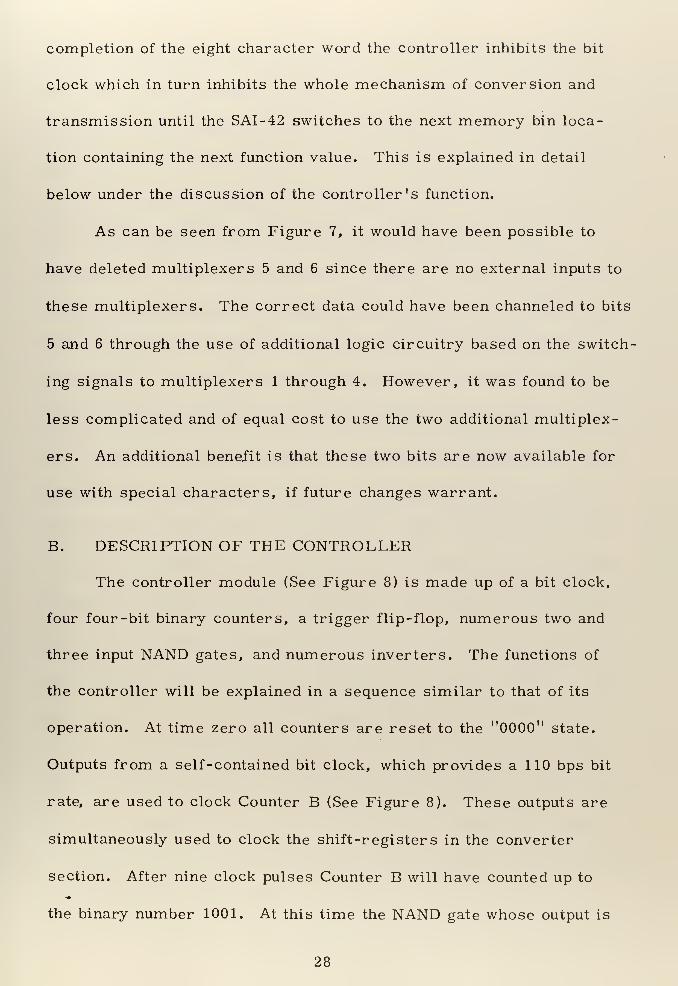
As can be seen from Figure 7, it would have been possible to
have deleted multiplexers 5 and 6 since there are no external inputs to
these multiplexers. The correct data could have been channeled to bits
5 and 6 through the use of additional logic circuitry based on the switch-
ing signals to multiplexers 1 through 4. However, it was found to be
less complicated and of equal cost to use the two additional multiplex-
ers. An additional benefit is that these two bits are now available for
use with special characters, if future changes warrant.
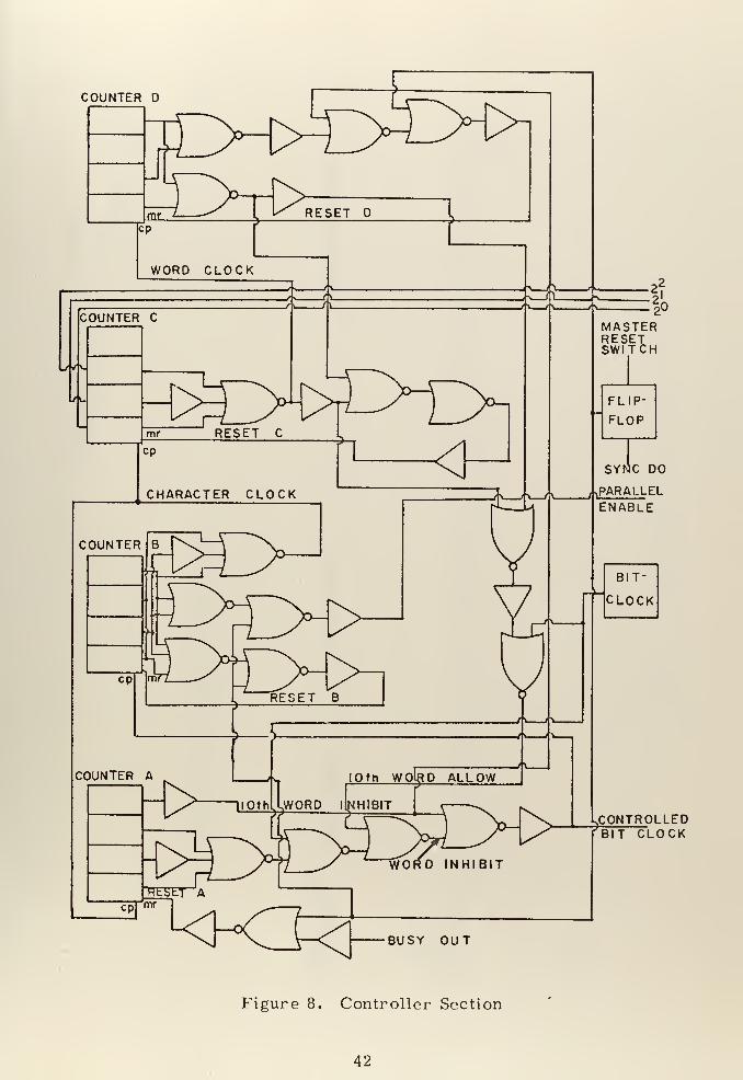
B. DESCRIPTION OF THE CONTROLLER
The controller module (See Figure 8) is made up of a bit clock,
four four -bit binary counters, a trigger flip-flop, numerous two and
three input NAND gates, and numerous inverters. The functions of
the controller will be explained in a sequence similar to that of its
operation. At time zero all counters are reset to the "0000" state.
Outputs from a self-contained bit clock, which provides a 110 bps bit
rate, are used to clock Counter B (See Figure 8). These outputs are
simultaneously used to clock the shift-registers in the converter
section. After nine clock pulses Counter B will have counted up to
the binary number 1001. At this time the NAND gate whose output is
28


labeled "Character Clock" is enabled. Enabling causes the output of
this NAND gate to change from logic level "l" to "0. " On the next
clock pulse three things occur simultaneously. First, the NAND
gate's output again changes from a "0" to a "l. " Since the counters
respond to the leading edge of a rising pulse a word clock pulse is
generated causing Counter C to be clocked to the "0001" state.
Secondly the "1010" state of Counter B allows the output of the inverter
labeled "Parallel Enable" to change from a "1" to a "0. " Finally the
2 , 2 , and 2 bits of Counter C are used as switch inputs for the
multiplexers. Counter C changing from "0000" to "0001" causes the
multiplexers to switch to input 1. The parallel enable state, i.e., a
"0, " prepares the shift-registers to accept new information from the
multiplexers on the next clock pulse. The next clock pulse causes
Counter B to register 1011 or 11 decimal. This state of Counter B
coincides the eleventh bit being shifted into the ASR-33 and causes the
output of the inverter labeled "Reset B" to change from a "l" to a "0"
which in turn causes Counter B to be reset to the "0000" state. The
next character has by now been channeled into the shift-registers and
the sequence is repeated. The change of the Reset B inverter from
"l" to a "0" and subsequently back to a "l" on reset causes a clock
pulse to be sent to Counter A. Clock pulses to Counter A occur two bit
times later than do clock pulses to Counter C. At this point Counter A
is in state "0001, " Counter B in state "0000, " Counter C in state "0001, "
and Counter D in state "0000. "
29


The above sequence of events repeats itself until the fifth char-
acter, the units place of the function value, has been transmitted to
the ASR-33. The character clock pulse that occurred at the change to
the "1001" state of Counter B during the fifth character's transmission
to the ASR-33, causes the output of the NAND gate labeled "Word Clock"
to change from a "1" to a "0. " This also causes the inverter labeled
"Reset C" to change from a "1" to a "0. " This "0" state of the Reset
C line causes Counter C to reset to the "0000" state which in turn
causes the output of the Word-Clock NAND gate to change from a "0"
to a "l. " This generates a word-clock pulse to Counter D causing it to
assume the state "0001. " The eleventh bit clock pulse again allows
multiplexer information to be sent to the shift-registers, Counter B to
reset itself, and a clock pulse to be sent to Counter A. Counter A is
now in the "0101" state. During all previously described events the
output of the bit clock had been channeled through a series of NAND-
gates which allowed the bit-clock pulses to continue as long as the state
of Counter A was not "0101. " Counter A now being in the "0101" state,
inhibits any further bit-clock pulses from continuing to Counter B or to
the shift-registers. Everything stops at this point until the SAI-42 has
switched to the next memory bin. Coincident with the SAI-42 's switch-
ing to the next memory bin the output of pin "r" the "Busy Out" pulse,
of the SAI-42 changes from a "0" to a "l. " This pulse is used to reset
Counter A to the "0000" state. The bit clock is now no longer inhibited
and the above described sequence of events is free to start over. At
30


this point Counter A is in state "0000, " Counter B in state "0000, "
Counter C in state "0000" and Counter D in state "0001. "
All the above events repeat themselves until the completion of
the transmission of the ninth word to the ASR-33. At this point Counter
D is in state "1001. " At the completion of the transmission of the fifth
character of the tenth word, when Counter C would normally reset and
Counter A would normally inhibit the bit clock pulses, these events are
themselves inhibited. This occurs because Counter D being in state
"1001" causes the NAND gate labeled "10th Word Allow" to gate bit-
clock pulses, bypassing the normal bit-clock inhibit gates. This state
of Counter D also causes the output of the NAND-gate labeled "Reset C
Inhibit" to change from a "l" to a "0. " This inhibits the resetting of
Counter C. The additional line feed carriage return, and "X-OFF"
characters are now allowed to be channeled sequentially to the shift-
registers and transmitted to ASR-33. The eleventh bit-clock pulse of
the transmission of the last character, "X-OFF, " of the tenth word
causes Counter B to again reset and to send a clock pulse to Counter
A. The state of Counter A is now "1000. " This state causes the out-
put of the inverter labeled "10th Word Inhibit" to change from a "1" to
a "0. " This overrides all bit-clock pulse gating circuits and inhibits
any further bit-clock pulses until the "Busy Out" pulse again arrives
from the SAI-42 to reset Counter A. Counter D is reset by the inverter
output labeled "Reset D" changing from a "1" to a "0. " This change is
calised by Counter D assuming the state "1010. " At this point all
31


counters are in state "0000" and the entire sequence is free to repeat
itself. Figure 9 shows the timing sequence involved in the transmis-
sion of the first ten words.
The above described sequence repeats itself until the 98th memory
bin's information has been transmitted to the ASR-33. Due to the design
of the SAI-42 its switching to its last memory bin, bin 99, is not accom-
panied by a "Busy Out" pulse. This prevents Counter A from being
reset to state "0000" and stops the entire process. Stopping at this
point precludes transmitting the information from memory bin 99. This
information could have been retrieved by including an additional counter
and logic circuitry but it was decided that the additional expense involved
in obtaining this last piece of data was not justifiable.
The purpose of the trigger flip-flop in the circuit is necessary to
ensure that all counters are reset to state "0000" at the beginning and
termination of operation. The presence of a master switch, a low
contact-bounce toggle switch, allows termination and resetting of the
process at any time. The "SYDC DO" pulse from the SAI-42 is avail-
able simultaneously with the SAI-42's switching memory bin 0. It is
used to reset all counters to state "0000" before operation begins. The
normal operating procedure is to reset the flip-flop to "0" with the tog-
gle switch, turn on the ASR-33 to the line mode, move the toggle switch
from the reset position, and then punch the SAI-42 read-out button. The
"SYNC DO" pulse causes the flip flop to trigger to state "l. " This re-
moves the continuous master reset from all counters and allows opera-
tion to begin.
32


The power for the integrated circuits is supplied from the SAI-
42 using output connecting pin P. Output connecting pin G is used to
provide a ground. Figure 10 is a schematic of the integrated circuit
design using symbology similar to that in the SAI-42 manuals.
C. MODIFICATION OF THE SAI-42
As mentioned earlier it was necessary to modify the logic
circuitry of the SAI-42 in order to allow the information from each
memory bin to be available for 1 sec vice 500 msec. In the original
SAI-42 circuitry the output of pin 1 1 of the decade counter in location
C-13 on IC card 4 is input into pin 14 of the decade counter in location
C-14 and into pin 2 of the quad two-input and/or gate in location C-18,
both also on card 4 (See Ref. 1). The modification entailed disabling
the output of pin 11 of C-13 into pin 2 of C-18 and using instead the
output of pin 1 of C-14 to input into pin 2 of C-18.
This modification did not require a direct change in the factory
wiring. The modification was achieved by mounting the integrated
circuits C-13, C-14, and C-18 in additional sockets and plugging the
sockets into the old sockets in a "piggy-back" fashion. Applicable
pins of the new sockets were removed so as not to make contact with
the pins of the old sockets and the necessary wiring between sockets,
as described above, was added. Applicable notation has been made on
the appropriate schematics for the Aeronautics Department's SAI-42
correlation and probability analyzer.
33


VII. SUMMARY
The interface design has been completely implemented in a
breadboard form and is being wired on integrated circuit cards.
When completely wired it will be a self-contained unit packaged in a
six inch square box.
The use of integrated circuitry has yielded a light weight, reliable,
compact interface. Although specifically designed to interface the SAI-
42 Correlation and Probability Analyzer and the ASR-33 Teletypewriter
Set it could be used to interface with the ASR-33 any device which pro-
vides a digital output. The Busy Out function of the SAI-42 in the word
and 10th word inhibits would have to be manually provided with a five
volt pulse. The design could easily be modified to allow a four digit
function value to be transmitted.
Cost for the integrated circuitry was $74.59. Additional costs
included $19.50 for the integrated circuit cards and plugs and $80. 00
for the 110 Hz bit clock.
34


SEND (RED)
COMMON (GRN)
RECEIVE (BLK)
3KH r-AA\
DATAFROMTTY.
-O-, DATA
! TTY.
or
EXTERNAL EQUIPMENT
Figure 1. Teletypewriter and External Equipment
35


o© o O o © © • © © o o © G © © 9
o G o © G © o • © © © © © © © 9o o o o o o o o o o o o O o o o o o o o o o o o o o o o o o o
o © © 9 o © © 9© © © © © © o 9 © o o o o © © 9
rrn— — —
\
" o o oK t- H- t- - »-
O o o o
P ¥—
"9
9 9m _9 9_ ©
mm3ms\6nm9\^<msm.BAiBr3DE:aGiHrjaKggiroM^sasauivMaYizB\HH^-
Figure 2a. ASCII Code Character Arrangement
STARTNO. NO. NO. NO. NO. NO. NO. NO. STQ p
Figure 2b. Current Waveform for Letter "U
36


1. INVERTER TRUTH TABLES
1
1
2. NAND GATE B
B
3. AND GATE
k. OR GATE
5. J-K FLIP-FLOP
I I f
1
1 1
1 1
1 1
A B X
1
1
1 1 1
A B X
1 1
1 1
1 1 1
r~n
Functions
Set Clear Output
X
1
1 1
1 1 X
Figure 3. Logic Elements
37


+127 -654 +879 +778 +569 +432 -487 -200 -382 -566
-075 -567 +254 +770 +432 +920 -021 -116 -567 +776
+921 +823 +678 +103 -001 -574 -982 -885 +886 +998
+456 +997 +554 +104 -119 -445 -973 -667 +997 +483
+872 +058 +992 +883 -895 -104 -003 +889 +457 +789-673 -863 -992 -198 -915 +975 +834 +105 +910 -783
-785 -006 +784 +110 +664 +863 -666 -987 -456 -873
+870 +089 +016 +804 +118 +543 -034 -996 -383 -116
+187 -678 +834 +654 +034 +862 +116 +874 -883 -444
-456 +119 +568 +836 +876 -167 -035 -873 +195
Figure 4. Data Format on Teletype Unit
38


SAI-42
MULTIPLEXERS
SHIFTREGISTERS
C ONVERTER
TIMING SWITCHIN G
CONTRO LL E R
Figure 5. Converter and Controller Block Diagram
39


STOP 8" B IT ASCII CODE START
SPACE 1 1 1
-f 1 1 1 1 1 1
—1 1 1 1 1 1
-91 1 1 1 * *- * -*
LINE
FEED 1 1 1 1
CARRIAGE
RETURN 1 1 1 1 1
X -OFF1 1 1 1 1
* Appropriate BCD Code for Numerals 0-9 Inserted Here
Figure 6. Required Teletype Code
40


TO ASR-33(0
SAI-42INPUTS
SIGNBl
CONTROLLEDBIT - CLOCK
PARALLELMPX- 6 ENABLE
Figure 7. Converter Section
41

COUNTER D
COUNTER A
cp
loth wqIrd allow"
INHIBIT
^CONTROLLEDBIT CLOCK
BUSY OUT
Figure 8. Controller Section
42


UJo z< CD£L —
o<_l UjUJ
a. o°V) 35
OUJ
o UJ
UJ u.
a:o UJ
z z — z3 UJ zX 1- 3 _J
a:
h-
UJ
<T
UJ
<!>
or u.
en o
a x
— CVJIO<frW tt> N CD
CO
uj
O<<Xo
a:
ul
HO<
<Xo
ce
UJ
a.
to1-
CO
ZUJ
>UJ-IUJ
CO
_CD
JO
to
C\J
~)fc
en
10
ro
in
ro
T<
CM
CM
0>
OC<v
CD
wtwo
coCO
CO
CO
H
CD
Sh
GtUiUJ UI- ZO uj
Jul
IdoZUJ
ee oo uj^ v>
UJ o2 uj— (/>
43


15 9312
II 1,21,3
15 9312
'. 1.2 3
HIS 9312
II 12 12
r 15 9312
II 12 13
:
—
|lO 93003
12
942
i—|I0 93003
Si 5 7
r 15 9312
II 12 13
r 15 9312
II 12 13
P 4 52
H'° 93003
B Oi
a 02
B 04 COI
Tl8
I
9099 B07
BIT-CLOCK
12
.TO TRANJSWITCH
COS
Figure 10. Entire Design Schematic
44


REFERENCES
1. Signal Analysis Industries Corp. , Instruction Manual, Correla-tion and Probability Analyzer, Model SAI-42 .
2. Teletype Corporation Bulletin 2 73B, Vol. 1, Technical Manual32 and 33 Teletypewriter Sets, Keyboard Send-Receive (KSR) ,
Receive-Only (RO), Automatic Send-Receive (ASR), November1964.
3. Naval Postgraduate School Computer Center Technical Note No.0211-18, Teletype User's Guide for CP/CMS and ProcessingPaper Tape Under CP/CMS, by Pimporn C. Zeleny, January1972.
4. Fairchild Semiconductor, Fairchild Semiconductor Integrated
Circuit Data Catalog 1970 .
5. Heath Company, Heath Modular Digital System, EU-801 Series ,
12 February 1970.
45


INITIAL DISTRIBUTION LIST
No. Copies
1. Defense Documentation Center 2
Cameron Station
Alexandria, Virginia 22 314
2. Library, Code 0212 2
Naval Postgraduate SchoolMonterey, California 93940
3. Professor L. V. Schmidt, Code 57 SX 2
Department of AeronauticsNaval Postgraduate School
Monterey, California 93 940
4. Chairman, Department of Aeronautics 1
Naval Postgraduate School
Monterey, California 93940
5. Lt. Arthur H. Collier 2
1576 Hillside TerraceAkron, Ohio 44305
46


UnclassifiedSecurity Classification
DOCUMENT CONTROL DATA -R&D(Security classilicat ion of title, body of abstract and indexing annotation must be entered when the overall report is classified)
1 originating ACTIVITY (Corporate author)
Naval Postgraduate School
Monterey, California 93940
2a. REPORT SECURITY CLASSIFICATION
Unclassified2b. GROUP
3 REPORT TITLE
An Interface Between the SAI-42 Correlation and Probability Analyzer
and the ASR-33 Teletypewriter Set
4. DESCRIPTIVE NOTES (Type of report and.inclusive dates)
Master's Thesis: March 19725. AUTHORISI (First name, middle initial, last name)
Arthur Hugh Collier
6 REPOR T D A TE
March 1972Sa. CONTRACT OR GRANT NO.
b. PROJEC T NO.
7a. TOTAL NO. OF PAGES
48
7b. NO. OF REFS
9a. ORIGINATOR'S REPORT NUMBER(S)
9b. OTHER REPORT NOISI (Any other numbers that may be assignedthis report)
10. DISTRIBUTION STATEMENT
Approved for public release; distribution unlimited.
II. SUPPLEMENTARY NOTES 12. SPONSORING MILITARY ACTIVITY
Naval Postgraduate School
Monterey, California 93940
13. ABSTRAC T
The purpose of the interface device is to make possible the
collection or storage of data from a laboratory instrument in punched
paper tape format, suitable for subsequent transmission to a digital
computer.
Important aspects of the interface design are presented and
problems encountered in this design are discussed. The micrologic
digital design is presented and its operation discussed.
DD, Fr..1473S/N 0101 -807-681 J
(PAGE 1)
47UnclassifiedSecurity Classification
A-31408


UnclassifiedSecurity Classification
key wo R OSLINK A
SAI-42 Correlation and Probability
Analyzer
ASR-33 Teletypewriter Set
Livermore Data Systems, Inc.
,
Acoustic Coupler
Micrologic Digital Design
Interface
Online Data Aquisition Under OS/360
FORMi nov e,1473 < BACK
i
0101 - 807- 68?
1
48UnclassifiedSecurity Classification A- 31 409


4 ocr 73
i 7 (
233
Thesis 133936C537 Collierc.l An interface between
the SAl-42 correlationand probability analy-zer and the ASR-33teletypewriter set
>4 0CT7S 2V3627 5 2 3 3' 936
tweenat ion
Thesis 133936CS37 Collierc.l An interface between
the SAI-42 correlationand probability analy-zer and the ASR-33teletypewriter set.

thesC537
An interface between the SAI-4?
""""Illlll'lllilllll'illiiilllllllllllllliiiiir
correlat
'HHI3 2768 002 08372 7DUDLEY KNOX LIBRARY
Top Related