


Languages
Pages
Legal

University of Texas at TylerScholar Works at UT Tyler
Electrical Engineering Theses Electrical Engineering
Fall 11-2011
An Evaluation of CMOS Adders for Robustnessand Fault Detectability in Nanoscale TechnologiesSowjanya Puttagunta
Follow this and additional works at: https://scholarworks.uttyler.edu/ee_grad
Part of the Electrical and Computer Engineering Commons
This Thesis is brought to you for free and open access by the ElectricalEngineering at Scholar Works at UT Tyler. It has been accepted forinclusion in Electrical Engineering Theses by an authorized administratorof Scholar Works at UT Tyler. For more information, please [email protected].
Recommended CitationPuttagunta, Sowjanya, "An Evaluation of CMOS Adders for Robustness and Fault Detectability in Nanoscale Technologies" (2011).Electrical Engineering Theses. Paper 4.http://hdl.handle.net/10950/48

An Evaluation of CMOS Adders for Robustness and Fault Detectability in
Nanoscale Technologies
by
SOWJANYA PUTTAGUNTA
A thesis submitted in partial fulfillment
of the requirements for the degree of
Master of Science in Electrical Engineering
Department of Electrical Engineering
David H. K. Hoe, Ph.D., Committee Chair
College of Engineering and Computer Science
The University of Texas at Tyler
November 2011

The University of Texas at Tyler
Tyler, Texas
This is to certify that the Master’s Thesis of
SOWJANYA PUTTAGUNTA
has been approved for the thesis requirements on
November 9, 2011
for the Master of Science Degree in Electrical Engineering
Approvals:
________________________________________
Thesis Chair: David H. K. Hoe, Ph.D.
________________________________________
Member: Mukul V. Shirvaikar, Ph. D.
________________________________________
Member: Hector A. Ochoa, Ph.D.
__________________________________________________
Chair and Graduate Coordinator: Mukul V. Shirvaikar, Ph. D.
_____________________________________________
Dr. James K. Nelson, Jr., Ph.D., P.E.,
Dean, College of Engineering and Computer Science,
Brazzel Professor of Engineering

Acknowledgements
At the outset, I sincerely thank god for bestowing me with his eternal blessings
with which I could successfully complete the task. Secondly, I am heartily thankful to my
family members: my father Dr. BhaskaraRao Puttagunta, mother Usha Rani Puttagunta,
brother Vasu Deva Prasad Puttagunta and my beloved fiancee Siva Vishnu Adusumilli
for their love, support and encouragement to complete my Master’s Degree. I would like
to express my sincere gratitude to my advisor Dr. David Hoe for his motivation,
continuous supervision and support to me without whom this would not be accomplished.
His guidance helped me during research and writing of this thesis. I thank my fellow
labmate and friend, Rahul Jesuran Gera for spending his precious time throughout my
research, working with a few sleepless nights before the deadlines and the fun we have
had in the lab. Also I am grateful to Sriram Boppana who is one among my supporters all
through my Master’s degree program.
My sincere thanks to the committee members, Dr. Hector Ochoa and Dr. Mukul
Shirvaikar for spending their valuable time in reviewing my work. I am grateful to Dr.
Mukul Shirvaikar through whom I got admitted into this Master’s Degree program and
also for his support to me throughout my Master’s degree. Also I thank the entire EE
department and the University of Texas at Tyler for helping me all through my degree.
Last but not the least; I would like to thank all those who supported me in any respect
during the completion of the thesis.
i
Table of contents
List of Tables ..................................................................................................................... iv
List of Figures .................................................................................................................... vi
Abstract ............................................................................................................................ viii
Chapter One : Introduction ................................................................................................. 1
1.1 Implementation of Adders ......................................................................................... 2
1.2 Research Objective .................................................................................................... 3
1.3 Research Procedure ................................................................................................... 4
1.3.1 Performance of 10T and 14T .............................................................................. 4
1.3.2 Robustness .......................................................................................................... 4
1.3.3 Fault Tolerance ................................................................................................... 5
1.4 Thesis Outline ........................................................................................................... 5
Chapter Two : Implementation of 10T and 14T Adders..................................................... 6
2.1 Adder implementation ............................................................................................... 6
2.1.1 Designing the layout of 10T and 14T ................................................................. 6
2.1.2 Assigning the capacitance values ....................................................................... 9
2.1.3 Extraction of the SPICE netlist ........................................................................... 9
2.2 Simulations .............................................................................................................. 10
2.2.1 Worst case......................................................................................................... 10
2.2.2 Calculation of delays with capacitive load ....................................................... 12
2.2.3 Calculation of delays with voltage scaling ....................................................... 14
2.2.4 Calculation of power ........................................................................................ 18
2.3 Summary ................................................................................................................. 20
Chapter Three : Robustness .............................................................................................. 21
3.1. Variation of the and .............................................................................. 21
3.1.1. Calculation of the change in for the 90 nm technology node .................. 22
3.1.2. Determining the technology dependent coefficients and ..................... 23
3.1.3. Extraction of model files with the parameter variations .................................. 25
ii
3.2 Simulation and Results ............................................................................................ 26
3.2.1 I-V curves for FF, Nominal and SS model files ................................................... 26
3.2.2 Calculation of Delays ....................................................................................... 28
3.3 Summary ................................................................................................................. 35
Chapter Four : Fault Tolerance ......................................................................................... 36
4.1 Fault Detection ........................................................................................................ 36
4.1.1 Stuck-open and stuck-short faults models ........................................................ 36
4.1.2 Classification of the faults ................................................................................ 39
4.1.3 Testing................................................................................................... 40
4.2 Analysis ................................................................................................................... 41
4.2.1 10T .................................................................................................................... 43
4.2.2 14T .................................................................................................................... 45
4.2.3 TGA .................................................................................................................. 47
4.2.4 CPL ................................................................................................................... 50
4.2.5 Static CMOS ..................................................................................................... 54
4.2.6 HCMOS ............................................................................................................ 57
4.3 Discussion ............................................................................................................... 60
4.4 Summary ................................................................................................................. 62
Chapter 5 : Conclusion and Future Work ......................................................................... 64
5.1 Conclusion ............................................................................................................... 64
5.2 Future work ............................................................................................................. 65
References ......................................................................................................................... 67
Appendix A: Worst Case Calculations ............................................................................. 69
1. 10T full adder worst case calculations figure ........................................................ 69
2. 14T full adder worst case calculations - figure ...................................................... 70
Appendix B: SPICE netlist for 10T and 14T full adders .................................................. 71
1. 10T adder with capacitive load at output ............................................................... 71
2. 14T adder with capacitive load at output ............................................................... 73
3. Fan out of four at output with supply voltage variation for 14T adder .................. 76
4. Fan out of four for power dissipation calculations for 14T adder ......................... 81
APPENDIX C: Model Files Extracted from PTM Tool ................................................... 89
iii
1. Selection of the MOSFET type and the technology node ...................................... 89
2. Assigning the parameter variations ........................................................................ 89
3. Extracted model files ............................................................................................. 89
APPENDIX D: SmartSpice code for Testing ..................................................... 136

iv
List of Tables
Table 2.1 Parasitic capacitance values for different technology nodes………………. 10
Table 2.2 Critical (C), Medium critical (MC) and Non critical (NC) paths of 10T
adder……………………………………………………………….………..
11
Table 2.3 Critical (C), Medium critical (MC) and Non critical (NC) paths of 14T
adder……………………………………………..……………….………...
12
Table 2.4 Delays for the respective in 90 nm technology node for 10T …….… 13
Table 2.5 Delays for the respective in 90 nm technology node for 14T ….…… 13
Table 2.6 Delays for the respective supply voltages in 90 nm technology node for
14T………………………………………………………………………….
17
Table 2.7 Power dissipation as a function of supply voltage for the 90 nm
technology node for 14T …………..……………………………………….
19
Table 3.1 Threshold variations………………………………………………………... 22
Table 3.2 Parameter variations in PTM………………………………………………. 25
Table 3.3 Supply voltages for different technology nodes…………………………… 26
Table 3.4 Rise time and fall time delays in 32 nm technology node…………………. 29
Table 3.5 Rise time and fall time delays in 45 nm technology node…………………. 29
Table 3.6 Rise time and fall time delays in 65 nm technology node…………………. 30
Table 3.7 Rise time and fall time delays in 90 nm technology node…………………. 30
Table 4.1 Classification of faults……………………………………………………... 40
Table 4.2 Combination of the inputs and its resulting outputs……………………….. 43
Table 4.3 Fault detection analysis of 10T full adder………………………………….. 43
v
Table 4.4 Fault detection analysis of 14T full adder………………………………….. 45
Table 4.5 Fault detection analysis of TGA full adder………………………………… 47
Table 4.6 Fault detection analysis of CPL full adder…………………………………. 50
Table 4.7 Fault detection analysis of static CMOS full adder………………………... 54
Table 4.8 Fault detection analysis of HCMOS full adder…………………………….. 58
Table 4.9 Overall grading of full adder designs……………………………...……….. 60

vi
List of Figures
Figure 1.1 CMOS Inverter…………………...………………………………….……. 2
Figure 1.2 4-bit Ripple Carry Adder …...…………………………………………….. 3
Figure 2.1 10T Full adder (a) Circuit schematic (b) Stick diagram (c) Layout ..…….. 7
Figure 2.2 14T Full adder (a) Circuit schematic (b) Stick diagram (c) Layout..……... 8
Figure 2.3 Load versus Delay of 10T, 14T, static CMOS and TGA full adders in 90
nm technology node……………………………………………………......
14
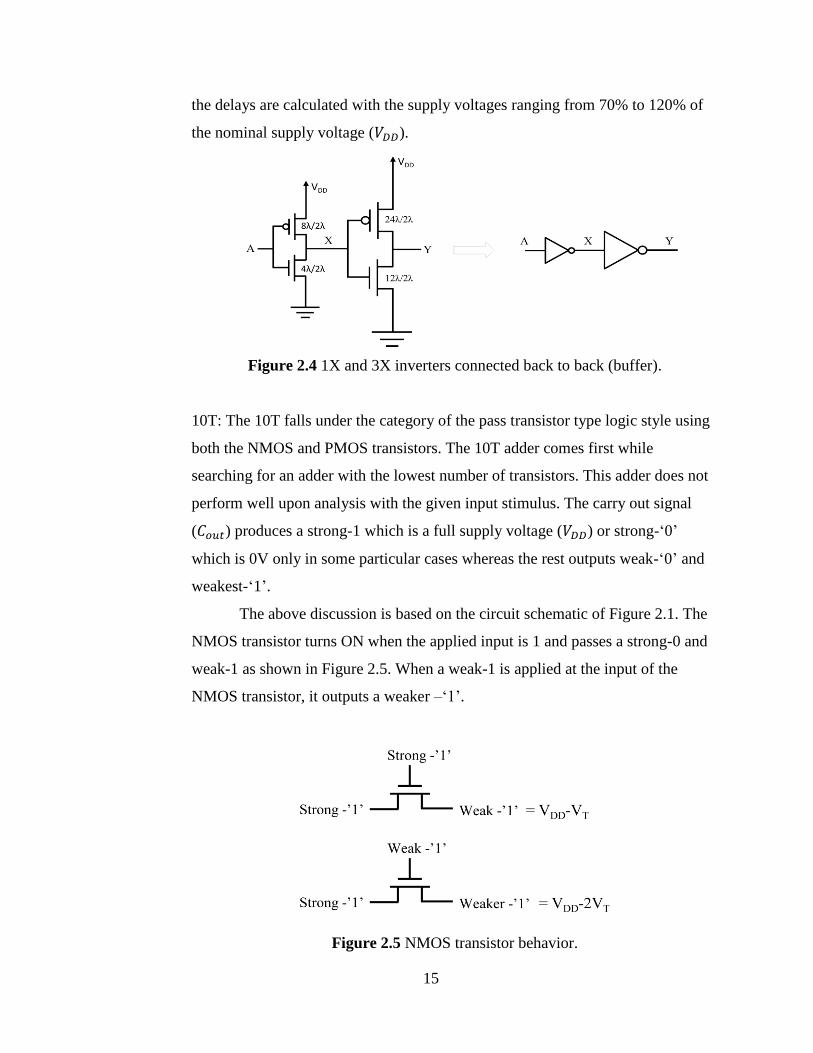
Figure 2.4 1X and 3X inverters connected back to back (buffer)…………………….. 15
Figure 2.5 NMOS transistor behavior………………………………………………… 15
Figure 2.6 Timing problems in logic implementation of the 10T full adder…………. 16
Figure 2.7 Delay versus respective voltages for TGA, static CMOS and 14T adders
in 90 nm technology node………………………………………...……….. 18
Figure 2.8 Circuit to measure power dissipation……………………………………... 18
Figure 2.9 Power versus supply voltage for static CMOS, TGA and 14T full adders
in 90 nm technology node………………………………………………….
20
Figure 3.1 Plot of fitting parameters C1 and C2……….……………………………… 24
Figure 3.2 I-V characteristics for NMOS and PMOS in 32 nm technology node……. 27
Figure 3.3 I-V characteristics for NMOS and PMOS in 45 nm technology node……. 27
Figure 3.4 I-V characteristics for NMOS and PMOS in 65 nm technology node……. 27
Figure 3.5 I-V characteristics for NMOS and PMOS in 90 nm technology node……. 28
Figure 3.6 32 nm technology node (a) Rise time delays (b) Fall time delays………… 31
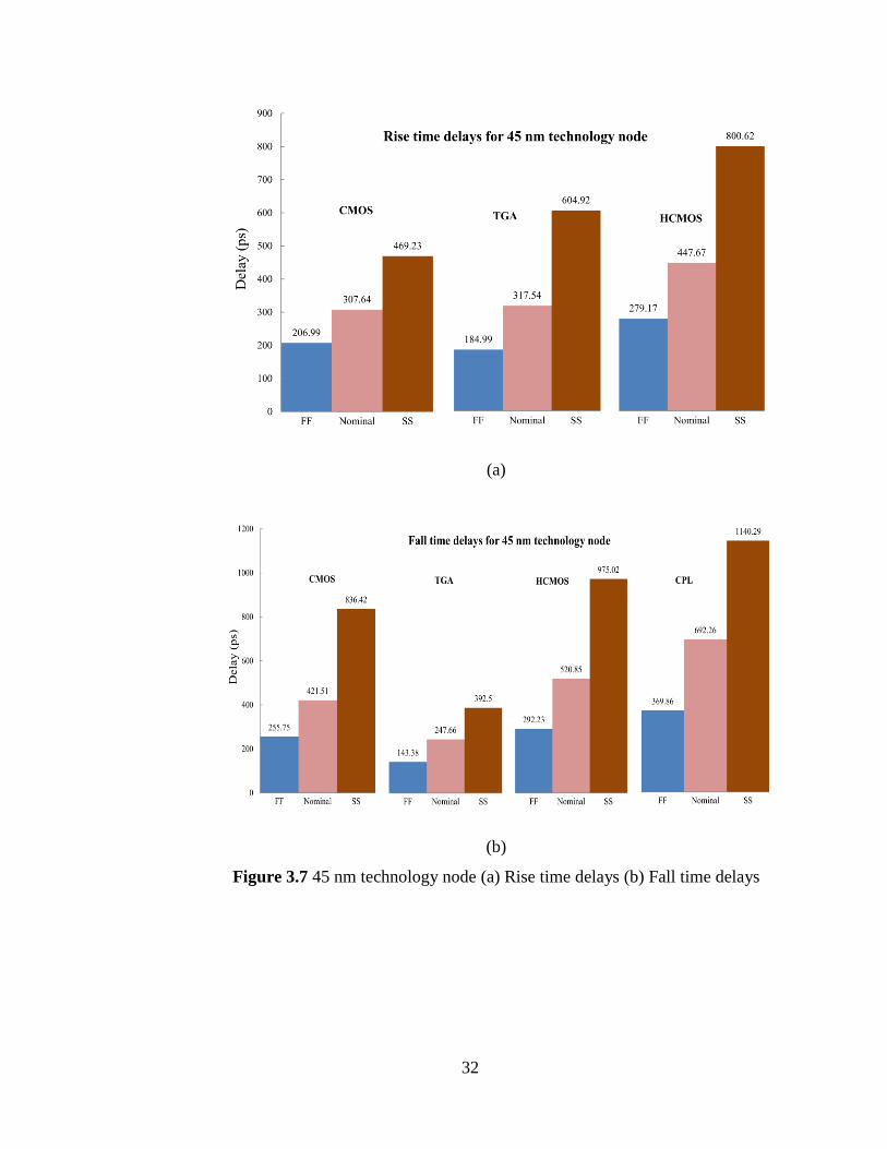
Figure 3.7 45 nm technology node (a) Rise time delays (b) Fall time delays………… 32

vii
Figure 3.8 65 nm technology node (a) Rise time delays (b) Fall time delays………… 33
Figure 3.9 90 nm technology node (a) Rise time delays (b) Fall time delays………… 34
Figure 4.1 (a) Single stuck-open MOSFET (b) Single stuck-short MOSFET……...… 36
Figure 4.2 A CMOS NOR circuit…………………………………………………….. 37
Figure 4.3 Circuit schematics of adders (a) CMOS (b) TGA (c) CPL (d) HCMOS (e)
10T (f) 14T………………………………………………………….……...
39
Figure 4.4 Circuit for testing ………………………………………………….... 41
Figure 4.5 Plot of (a) Supply current versus resistance (b) Output voltage versus
resistance…………………………………………………………………...
42
Figure 4.6 Fault detection of 10T full adder with transistor p1 “short” and input (A,
B, ) = (1, 0, 0).…………………………………………………………..
44
Figure 4.7 Fault detection of 14T full adder with transistor p1 “open” and input (A,
B, ) = (1, 0, 0)…………………….……………………………………..
47
Figure 4.8 Fault detection of TGA full adder with transistor Mp5 “short” and input
(A, B, ) = (0, 1, 1)…………………………..…………………………..
50
Figure 4.9 Fault detection of CPL full adder with transistor Mn3 “short” and input
(A, B, ) = (0, 1, 0)……………..……………………………………….
53
Figure 4.10 Fault detection of CPL full adder with transistor Mn4 “open” and input
(A, B, ) = (0, 0, 0)……..………………………………………………
54
Figure 4.11 Fault detection of static CMOS full adder with transistor Mp6 “short”
and input (A, B, ) = (1, 1, 1)…………..…………………..…………..
57
Figure 4.12 Fault detection of HCMOS full adder with transistor P10 “open” and
input (A, B, ) = (0, 1, 0)……..………………………………………...
60
Figure A.1 Worst case paths for 10T full adder………………………………………. 69
Figure A.2 Worst case paths for 14T full adder………………………………………. 70

viii
Abstract
An Evaluation of CMOS Adders for Robustness and Fault Detectability in
Nanoscale Technologies
Sowjanya Puttagunta
Thesis Chair: David H. K. Hoe, Ph.D.
The University of Texas at Tyler
November 2011
The objective of this thesis is to implement the two low transistor count
full adders using submicron CMOS technologies and to study their performance
with respect to process variations and single-transistor faults. One adder uses 10
transistors and the other uses 14 transistors. Hence they are respectively called the
10T and 14T adders. Previous work has studied the implementation of the static
Complementary Metal Oxide Semiconductor (CMOS) adder, Complementary
Pass Transistor Logic (CPL) adder, Transmission Gate adder (TGA) and the
Hybrid CMOS (HCMOS) adder. The performance of the 10T and 14 T adders
using the above mentioned metrics are compared with these adders and
conclusions are made as to which adders are the best candidates for
implementation in nanoscale technologies.
The method for implementing the 10T and 14T full adders includes the
analysis of the circuit schematic and the construction of its physical layout using
the Electric layout design tool. The netlists are extracted with the assigned
parasitic capacitances and are simulated to calculate the delays with different
ix
capacitive loads and the variations in the supply voltage. The power dissipation is
calculated using a fan-out-of-four load. This same circuit configuration is also
used to calculate the delays for a range of supply voltages.
As deep submicron technologies are known to experience increasingly
larger variations in process parameters, their impact on the performance of the
CMOS, CPL, TGA, HCMOS, 10T and 14T full adders is studied. The Fast
NMOS and Fast PMOS design corner, nominal and Slow NMOS and Slow
PMOS design corner model files are generated for different technology nodes
with the process variations using the Predictive Technology Model (PTM)
website and the respective delays are calculated for all the adders.
The adders are analyzed for fault detectability by using a stuck-open and
stuck-short Metal Oxide Semiconductor Field Effect Transistor (MOSFET) fault
model. After examining the effect of such faults on each MOSFET in the adders
under study, they are ranked according to the ease with which a fault can be
detected. The effect of fault analysis using the quiescent supply current ( )
testing is also studied.
Previously, these adders were studied at 180 nm node or above. The
contribution of this thesis is the comprehensive analysis of the above mentioned
adders for process variations and fault detectability in deep submicron processes.
Specific results from this study include the following: the low transistor count
adders (10T and 14T) do not scale well in terms of delay performance when
implemented in nanoscale CMOS technologies. The main reason is the reduction
in power supply voltage that is mandated in the deep submicron regime. This has
a detrimental effect on the signal paths that use only a single transistor pass gate.
This situation frequently occurs in adder circuits that attempt to minimize the
transistor counts. As for fault detectability, previously there has been no
comprehensive study of the adders in this regard. Some specific conclusions from
this work include the following: it is found that the best adder circuits allow the
memory states that occur when a transistor is stuck open to be effectively utilized.
The singular paths of the 10T adder and the complementary logic networks of the

x
static CMOS adder allowed them to be ranked highest for detectability. In terms
of performance with respect to process variation and delay, the TGA adder and
static CMOS adders performed best. In summary, this thesis provides some
important guidelines for implementing adder circuits in nanoscale CMOS
technologies. Specifically, circuits that ensure full voltage swings at all internal
nodes by using full CMOS transmission gates (TGA) or complementary logic
trees (static CMOS) are the best candidates for implementations in deep
submicron processes.

1
Chapter One
Introduction
A world without electronics cannot be imagined in the present generation.
The use of electronic items has encompassed our regular work day to such a
degree that it is impracticable to spend a few hours without them. At the outset of
the day to its end, we use a battalion of electronic gadgets to enhance various
problem solving activities. In sum, we are very dependent on the electronics, as
they facilitate our day to day lifestyle. For example, the use of mobile phones has
changed the definition of communication. The Smartphone was introduced to the
public in 1993, with added features like: gaming, email, etc. Instead of physical
buttons, the users touch the screen to select the required options. Researchers
found that its usage has had a rapid increase from the year 2006 till present [1].
According to a recent survey, 77 percent of the world population uses the mobile
phone [2]. Also we use a variety of portable electronic devices which are inbuilt
with a variety of operating systems. It is difficult for us to imagine the world
without electronic devices.
Digital Signal Processing (DSP) is commonly used in devices such as
mobile phones, laptops, multimedia computers, camcorders, CD players, hard
drives etc. A DSP chip is a programmable device, which has a set of instructions
that enable various algorithms to be coded into it. The adder is one of the key
components of a DSP chip. Recent devices like microprocessors have become
quite powerful with the ability to perform millions of operations per second. As
the number of transistors on a chip increases, the power consumption becomes a
concern especially for use in portable electronics.

2
1.1 Implementation of Adders
A Complementary Metal Oxide Semiconductor (CMOS) process is the
latest and the most common VLSI technology, which consists of several design
features that are advantageous for digital circuit design. The ease of design, good
noise margin, low static power and robustness results in the popularity of CMOS.
In addition to the advantages, it also exhibits some disadvantages. In standard
static CMOS design, the NMOS transistor should be paired with the PMOS
transistor to ensure fully complementary operation. However, this increases the
number of transistors in the circuit. Also, the size of the PMOS transistor has to
be bigger as it has a lower carrier mobility compared to the NMOS device. This
increases the overall area of the circuit. Taking these disadvantages into
consideration, researchers have looked at other logic families like the
Complementary Pass transistor Logic (CPL) which consists only of NMOS
transistors. This has resulted in various adder designs, including the Transmission
Gate Adder (TGA), 10T and 14T which consist of a small transistor counts and a
couple of other logic families [3].
A static CMOS gate consists of a pull-up pMOSFET logic network and a
pull-down nMOSFET logic network with an nMOSFET. Figure 1.1 shows the
circuit of a CMOS inverter. The output (Y) of this inverter will be the negation of
its input (A). To support this basic functionality, when the input is high (i.e.,
A=1), the pMOS transistor will be OFF and the nMOS transistor will be ON
which discharges the input to the ground giving a zero output (Y=0). On the other
hand, when the input is low (i.e., A=0), the nMOS transistor will be OFF and the
pMOS transistor will be ON producing the supply voltage at the output (Y=1).
Figure 1.1 CMOS Inverter

3
The full adder is considered to be the basic building block of all the complex
arithmetic circuits like addition, multiplication, etc. Figure 1.2 represents the
block diagram of a 4-bit ripple carry adder which contains four full-adder cells.
Each carry-bit ripples to the next full adder, hence the name. This is
comparatively slow because each adder must wait to get the carry bit generated by
the previous one. It is required that the generation of the carry-out signal should
be very fast without which the worst case delay increases, creating more glitches
in the post stages [3]. Hence the optimization of the adder circuit should be done
to enhance its performance.
Figure 1.2 4-bit Ripple Carry Adder
1.2 Research Objective
The objective of this research is to evaluate the low transistor count 10T
and 14T adders in deep submicron technologies and to compare them with other
adder designs [3]. A logic gate is designed in many different ways using the
CMOS technology. Pass Transistor Logic (PTL) is a logic family which is used as
a substitute for static CMOS. The key difference between PTL and static CMOS
is that in the former, the source of the transistors is connected to the inputs rather
than the power rails. The PTL has an underlying problem of threshold voltage
drop. This problem has been overcome in Transmission Gate Adder (TGA) but it
requires almost double the number of transistors compared to PTL. The Hybrid
CMOS (HCMOS) is optimized for driving loads and is robust with low power in
4
deep submicron technology [4]. The analysis of the circuit and its optimization
are essential for a good CMOS design. For this precision design, the process
variation parameters are identified and scaled [5]. Process variation has a direct
impact on the variability of the circuit performance. The performance of the full
adder circuits with respect to the fault detecting ability will be undertaken as this
becomes an increasingly important issue in deep submicron technologies [6].
1.3 Research Procedure
The methods of evaluating the performance of 10T and 14T adders by the
calculation of the worst case delays and the fault detection for several adders are
reviewed in this section.
1.3.1 Performance of 10T and 14T
In this section, how the performance of the adders 10T and 14T will be
evaluated is described. First the schematic of the adder design is drawn and its
physical layout is created. The parasitic capacitances are included for each
technology node and the netlists are extracted individually from the layout after
its optimization. Each extracted netlist is simulated with different load
capacitances and the supply voltages and the results are analyzed.
1.3.2 Robustness
For optimization of the circuit, the process variation parameters need to be
recognized before being scaled. These parameters are identified to be the mobility
(µ), threshold voltage ( ) and the gate length (L) [4]. These are modified with
respect to the original technology model file and the best case, worst case and
nominal model files are generated using the Predictive Technology Model (PTM)
website [7]. The netlists that are extracted from the physical layout are simulated
using the newly generated model files and the respective worst case delays are
calculated.

5
1.3.3 Fault Tolerance
Whenever a fault occurs in a circuit, it functions abnormally i.e. it does not
yield the desired output. The fault behavior of the circuit is performed and
analyzed by fault analysis. The stuck-open and stuck-short faults are created for
each transistor and the circuit is analyzed by comparing the fault output with the
original [6]. Conclusions on the robustness of each adder with respect to fault
detectability are given.
1.4 Thesis Outline
In chapter 2, the implementation of the 10T and 14T full adders are
discussed and their performance in different technology nodes are analyzed.
Chapter 3 discusses the robustness of the different adder circuit designs. It also
describes the generation of the model files with the change in the process
variation parameters and calculation of the worst case delays. Chapter 4 considers
the fault behavior of the circuit design by inserting stuck-open and stuck-short
faults. Chapter 5 provides the conclusions and possible future work.

6
Chapter Two
Implementation of 10T and 14T Adders
A logic gate is designed in many different ways using CMOS technology.
Static CMOS is the most commonly used logic style which consists of a pull-up
logic network with a pMOSFET and a pull-down logic network with an
nMOSFET. Dynamic logic is also a commonly used logic style for high-speed
and reduced area circuit designs which uses either nMOSFET or pMOSFET
transistors. Pass Transistor Logic (PTL) is a logic family which is used as a
substitute for static CMOS. As the static CMOS uses both the NMOS and PMOS
transistors which increases the transistor count, researchers have proposed two
adders with small transistor counts, known as 10T and 14T [3]. This chapter
discusses the performance of the 10T and 14T adders using deep submicron
CMOS technologies. This includes the details of the simulations for calculating
the worst case delays and the power dissipation.
2.1 Adder implementation
To evaluate the adder designs in deep submicron technology, adequate
interconnect parameters are required for both the transistor and on-chip
interconnect. This section describes the procedure for creating the physical layout
of the adders. This includes the optimization of the transistor size’s and results in
the extraction of the netlist for use with the Simulation Program with Integrated
Circuit Emphasis (SPICE) software.
2.1.1 Designing the layout of 10T and 14T
The full adder logic style for 10T and 14T is selected from the literature
[3]. The circuit schematics are analyzed and the stick diagrams are sketched
which are used for optimization of the layout.

7
Figure 2.1 10T Full adder (a) Circuit schematic (b) Stick diagram (c) Layout.

8
Figure 2.2 14T Full adder (a) Circuit schematic (b) Stick diagram (c) Layout.

9
The physical layout is constructed using the Electric layout design tool with the
connections between the transistors as per the stick diagram. For accuracy of the
circuit performance, the parasitic effects need to be included in the analysis. The
parasitic capacitances are calculated for each technology node for metal and poly-
silicon as explained in Gera’s thesis [8]. The calculated parasitic parameters are
inserted in the physical layout design which allows the extraction of the netlists
including the capacitances due to interconnect for the adder design.
10T: As the name indicates, it contains a total of 10 transistors. The circuit
schematic [3], stick diagram and the physical layout are shown in Figure 2.1.
14T: As the name indicates, it consists of a total of 14 transistors. The circuit
schematic [3], stick diagram and the physical layout are shown in Figure 2.2.
2.1.2 Assigning the capacitance values
Once the physical layouts are drawn using the Electric layout design tool,
the parasitic capacitances for the metal and the polysilicon interconnect calculated
for the different technology nodes are entered into the design tool. This ensures
the parasitics associated with physical dimensions of the interconnect are included
in the netlist for accurate simulation. Table 2.1 [8] gives the capacitance values
used in this research.
2.1.3 Extraction of the SPICE netlist
The extracted SPICE netlist forms the basis for all the simulations. This is
extracted from the physical layout which consists of all the connections between
the transistors and the included parasitic capacitances for the specified technology
nodes. The code is altered to suit the required type of analysis. This includes the
addition of supply voltages and capacitive loads to perform the intended
simulations. Three bits i.e. (0, 0, 0) – (1, 1, 1) are given as the inputs (A, B, )
and are specified in the netlist. This is used to verify whether the extracted netlist

10
is representing the basic functionality of an adder and to calculate the delay from
the input to the output.
Table 2.1 Parasitic capacitance values for different technology nodes.
Technology Node
(nm)
90 65 45 32 22 16
Metal_1 Plate Capacitance
( ⁄ )
82.639 97.396 221.35 251.54 357.27 470.73
Total Fringe
Capacitance
( ⁄ )
209.534 164.631 187.085 185.325 208.085 227.912
Metal_2 Plate Capacitance
( ⁄ )
55.093 64.931 147.57 167.69 238.18 313.82
Total Fringe
Capacitance
( ⁄ )
16.1246 12.6694 14.397 15.2798 18.6462 21.164
Polysilicon Plate Capacitance
( ⁄ )
165.28 194.79 442.71 503.08 714.55 941.46
Total Fringe
Capacitance
( ⁄ )
148.776 117.998 139.633 133.932 146.916 155.776
2.2 Simulations
This section discusses the simulations used to characterize the adders. This
includes the delays with the capacitive load, the scaling of the supply voltage
( ) and the calculation of the power dissipation for a Fan-out of four (FO4)
load.
2.2.1 Worst case
The delay between the input and the output signal of a gate is called the
propagation delay. This section gives a detailed analysis of the 10T and 14T
adders in finding the worst case (WC) delay. The delays are calculated with the

11
change in the load capacitance ( ) and the supply voltage ( ). Table 2.2
and Table 2.3 represent the critical, the medium critical and the non-critical paths
for 10T and 14T adders respectively (see Appendix A). The successive
combination of all the possible critical paths is used to produce an input stimulus
waveform which is used to calculate the power dissipation.
The Non Critical (NC) path is where there is no change of output ( )
from one transition to another. The Medium Critical (MC) path is where
changes from one state to another, without any change in the internal nodes. The
Critical (C) path will be where there is a change in both and the internal
nodes.
Table 2.2 Critical (C), Medium critical (MC) and Non critical (NC) paths of 10T
adder.
Sl # Input stimulus – 1 Input stimulus – 2 Path
A B A B
1 0 0 0 0 0 0 1 1 NC
2 0 0 0 0 0 1 1 0 C
3 0 0 0 0 1 0 1 0 C
4 0 0 1 1 0 0 0 0 NC
5 0 0 1 1 0 1 1 0 C
6 0 0 1 1 1 0 1 0 C
7 0 1 1 0 1 0 1 0 NC
8 0 1 1 0 0 1 0 1 MC

12
Table 2.3 Critical (C), Medium critical (MC) and Non critical (NC) paths of 14T
adder.
Sl
#
Input stimulus – 1 Input stimulus - 2 Path
A B A B
1 0 0 0 0 0 0 1 1 NC
2 0 0 0 0 0 1 0 1 MC
3 0 0 0 0 0 1 1 0 C
4 0 0 0 0 1 0 1 0 C
5 0 0 1 1 0 1 0 1 MC
6 0 0 1 1 0 1 1 0 C
7 0 0 1 1 1 0 1 0 C
8 0 1 0 1 1 0 0 1 NC
9 0 1 0 1 1 0 1 0 MC
10 0 1 0 1 1 1 0 0 C
11 0 1 0 1 1 1 1 1 C
12 1 0 0 1 0 0 1 1 MC
13 1 0 0 1 1 1 0 0 C
14 1 0 0 1 1 1 1 1 C
2.2.2 Calculation of delays with capacitive load
The driving capability of the adder circuit is studied by adding an external
capacitive load. Unlike the case of voltage scaling, no FO4 circuit is attached at
the output to the drawn layout. The output connection is done manually in
the extracted netlist containing the worst case input stimulus waveforms. The
supply voltage is maintained constant at nominal and the load capacitance is
varied from no load capacitance i.e. zero capacitance to 100fF. As the 10T and
14T adders do not scale well with the technology nodes due to the requirement for
very low power supplies and the value of - is very low at lower technology
nodes, the simulations are carried out only for the 90 nm technology node.

13
10T: A variable capacitive load ( ) is placed at the output of the 10T adder
with a different supply voltage. The netlist is simulated using SmartSpice [9] with
the input stimulus and the worst case delays for each capacitive load. The results
are tabulated in Table 2.4 (see Appendix B).
Table 2.4 Delays for the respective in 90 nm technology node for 10T.
Technology node
(nm)
(fF) Rise time
(ns)
Fall time
(ns)
90
0 0.067161 0.10909
5 0.097661 0.14139
10 0.12033 0.16526
20 0.16922 0.21539
50 0.30321 0.32287
100 0.52837 0.50698
14T: The capacitive load ( ) at the output of the 14T adder is varied while the
supply voltage is held constant. The netlist is simulated with the input stimulus
and the worst case delays for each capacitive load. The results are tabulated in
Table 2.5 (see Appendix B).
Table 2.5 Delays for the respective in 90 nm technology node for 14T.
Technology node
(nm)
(fF) Rise time
(ns)
Fall time
(ns)
90
0 0.11753 0.10665
5 0.14054 0.13325
10 0.15563 0.14678
20 0.185 0.17297
50 0.26929 0.24782
100 0.41219 0.37189

14
A graph is plotted with the delay versus capacitive load with 90 nm
technology node for 10T, 14T, CMOS and TGA [8] adders as shown in Figure
2.3. The 14T adder performs better compared to static CMOS because in most of
the cases the output has a single transmission gate connecting the output to the
input. The feedback with the p3 and n3 transistors in the 14T adder ensures that
there is a full voltage swing on the internal nodes that drives the transmission
gates. This contrasts with the 10T adder where there is single PMOS or NMOS
path to the output. This results in degraded voltage swing ( - ) at both the
internal nodes and output in many cases. Hence the 10T adder has the worst load
versus delay characteristics for large capacitive loads.
Figure 2.3 Load versus Delay of 10T, 14T, static CMOS and TGA full adders in
90 nm technology node.
2.2.3 Calculation of delays with voltage scaling
As discussed in section 2.1.3, the Spice netlist is extracted from the
physical layout. To calculate the delay with the voltage scaling, an FO4 circuit is
attached at the outputs ( , Sum) of the original layout. The netlist is extracted
again to calculate the delay. Figure 2.4 represents the FO4 with the minimum size
inverter driving the inverter which is three times bigger. The netlist is modified by
adding the input stimulus waveforms for the FO4. It is simulated using SPICE and
0
0.1
0.2
0.3
0.4
0.5
0.6
0 50 100 150
Del
ay (
ns)
Capacitive Load (fF)
Load Vs Delay
10T
14T
static CMOS
TGA
15
the delays are calculated with the supply voltages ranging from 70% to 120% of
the nominal supply voltage ( ).
Figure 2.4 1X and 3X inverters connected back to back (buffer).
10T: The 10T falls under the category of the pass transistor type logic style using
both the NMOS and PMOS transistors. The 10T adder comes first while
searching for an adder with the lowest number of transistors. This adder does not
perform well upon analysis with the given input stimulus. The carry out signal
( ) produces a strong-1 which is a full supply voltage ( ) or strong-‘0’
which is 0V only in some particular cases whereas the rest outputs weak-‘0’ and
weakest-‘1’.
The above discussion is based on the circuit schematic of Figure 2.1. The
NMOS transistor turns ON when the applied input is 1 and passes a strong-0 and
weak-1 as shown in Figure 2.5. When a weak-1 is applied at the input of the
NMOS transistor, it outputs a weaker –‘1’.
Figure 2.5 NMOS transistor behavior.

16
The PMOS transistors are ON when the input is ‘0’ and passes a strong-1
and weak-‘0’ which is the converse of the NMOS transistor. Consider the case
when A=1, B=1 and =0 as shown in Figure 2.6(a) which is part of the 10T
design. As the inputs A and B are ‘1’, transistors p1 and p2 turns OFF (see Figure
2.1) and n1 and n2 are ON passing a weak-1through each of them which makes
node ‘h’ as a weak-‘1’. The node ‘h’ makes the transistors n5 and p5 partially
ON, which outputs a weaker-1 and weaker-‘0’ respectively. The resulting output
will be a weakest-‘1’ which is almost like a weak-‘0’ as shown in Figure 2.6. This
is the trade-off in trying to minimize the number of transistors and is especially a
problem when scaling the power supply due to - reduction in signal swing.
Figure 2.6 Timing problems in logic implementation of the 10T full adder

17
14T: The extracted netlist for the 14T adder is simulated using the SPICE
simulator [9] with a range of supply voltages. The output delay values with the
voltage ranging from 70%-120% are tabulated as shown in the Table 2.6.
Table 2.6 Delays for the respective supply voltages in 90 nm technology node for
14T.
Technology node
(nm)
Voltage
(V)
Rise time (ns) Fall time (ns)
90
1.0 0.17097 0.19563
1.1 0.1561 0.18204
1.2 0.14862 0.14272
1.3 0.1403 0.13121
1.4 0.1343 0.11567
1.5 0.12777 0.10502
The voltage versus rise time delay of the TGA and the static CMOS full
adders [8] are plotted along with the 14T adder as shown in Figure 2.7. The delay
of the 14T adder becomes very high as the power supply voltage scales down
because of the reduced signal swing at the first set of transistors (n1,n2,p1 and
p2). Although the feedback due to transistors p3 and n3 can restore the signal
swing, they become ineffective as the power supply approaches twice the
threshold voltage of the NMOS transistor ( ). This contrasts with the TGA
which performs best with reduced voltage supply because it has full
complementary transmission gates which doesn’t suffer from a reduced voltage
swing ( - ).

18
Figure 2.7 Delay versus respective voltages for TGA, static CMOS and 14T
adders in 90 nm technology node.
2.2.4 Calculation of power
The power calculation is also carried out with the same FO4 load at the
output as described in section 2.2.3. The power dissipation is measured by
connecting the full adder to the circuit shown in Figure 2.8, consisting of a
parallel connection of capacitor and resistor , which is connected to the
power supply ( ) at one end and a voltage device ( ) with voltage = 0V
at the other end. The netlist is extracted from the layout containing only the FO4
and the input buffers to the full adder. The values of and are inserted
manually into the netlist.
Figure 2.8 Circuit to measure power dissipation
0
0.02
0.04
0.06
0.08
0.1
0.12
0.14
0.16
0.18
0 0.5 1 1.5 2
Del
ay (
ns)
Voltage (VDD)
Voltage Vs Delay
TGA
static CMOS
14T

19
β = *
(2.1)
The value of ‘β’ is calculated from equation 2.1 where ‘T’ is the time
period between each iteration. The input stimulus waveform is manually entered
in the extracted netlist and is simulated by varying the supply voltage ( ). The
increasing step sizes obtained in the graph are the coefficients of the power
dissipated. The difference between the initial and the final step size is divided by
the number of steps to obtain the average power dissipation [10].
10T: As discussed in section 2.2.3, because of the timing problems in the logic
implementation of the 10T adder, the power dissipation is not calculated.
14T: Table 2.7 gives the values of calculated power for each simulation with the
corresponding supply voltages.
Table 2.7 Power dissipation as a function of supply voltage for the 90 nm
technology node for 14T.
Voltage (V) Initial step size
V1 (µV)
Final step size V2
(µV)
Power (µW)
1.0 0.78369 15.156 0.3593
1.1 0.87799 17.531 0.4163
1.2 0.92324 19.981 0.4764
1.3 1.047 22.768 0.5430
1.4 1.0987 25.714 0.6153
1.5 1.1788 29.116 0.6984
The power dissipation of the TGA and the static CMOS full adders which scale
well [8] are plotted along with the 14T adder in Figure 2.9.

20
Figure 2.9 Power versus supply voltage for static CMOS, TGA and 14T full
adders in 90 nm technology node.
2.3 Summary
The physical layouts of the 10T and 14T adders are designed using the
circuit schematic and the corresponding stick diagrams. The netlists from the
Electric layout design tool are extracted with the assigned capacitance values. The
worst case inputs are identified and are sequenced to result in an input stimulus
waveform which is supplied to the input terminals. The reason for the
imperfection in the implementation of the 10T adder was discussed. The delays
with varied , supply voltages and the dissipated power are calculated and
tabulated. The 14T full adder has lower power dissipation because it does not
have a full voltage swing and also contains fewer transistors resulting in smaller
nodal capacitance.
0
0.5
1
1.5
2
2.5
3
3.5
0 0.5 1 1.5 2
Po
wer
(µ
W)
Supply Voltage VDD (V)
Voltage Vs Power
Static CMOS
TGA
14T
21
Chapter Three
Robustness
In order to determine how robust the various adders are due to the process
variations, there is a need to identify the set of primary and independent process
variation parameters and to understand how they scale with respect to the
technology nodes under consideration [5]. This chapter discusses the key process
parameters and their variation with respect to the original technology file. These
model files are obtained from the Predictive Technology Model (PTM) website
[7]. The rise time and the fall time delays for the worst case and the best case
parameters are calculated through utilization of the SPICE simulator. These
delays are calculated for the CMOS, CPL, TGA and HCMOS adders for 32 nm,
45 nm, 65 nm and 90 nm technology nodes. As the existing literature does not
provide sufficient data for the 90 nm technology node [11], the change in the
threshold voltage ( ) for this node is estimated from published data at the
smaller technology nodes.
3.1. Variation of the and
The process parameters that need to be varied for circuit optimization are
mainly identified as the threshold voltage ( ) and the gate length ( ). The
threshold voltage ( ) is due to random dopant fluctuations in the channel which
becomes more severe as the channel volume decreases with scaling and the gate
length ( ) is due to subwavelength lithography and etching process steps. The
variations in the mobility (µ) are also significant in deep submicron technologies.
For example, the use of strained silicon technology to improve device
performance results in real fluctuations due to stress at the boundaries between
various heterogenous layers of silicon [5]. The International Technology
Roadmap for Semiconductors (ITRS) [12] provides a discussion of future trends

22
that are of interest to the semi-conductor industry. According to the ITRS road
map, the target for future technology nodes for maximum allowed variation in the
gate length ( ) is set to 10% [12]. Therefore, this maximum variability is used
to generate the best case and worst case model files for all technology nodes.
3.1.1. Calculation of the change in for the 90 nm technology node
The change in the threshold voltage ( ) is one of the prevailing
components of process variation. This is calculated for the 90 nm technology
node using the data from Table 3.1 which is obtained from [11].
Table 3.1 Threshold variations
LER parameters Total (mv)
WC (nm) (nm) 65 nm
( =1.1V)
45 nm
( =1V)
32 nm
( =0.9V)
22 nm
( =0.8V)
5 0 19.9 23.8 28.1 45.8
0.5 20.0 24.1 28.7 47.0
1 20.4 24.9 31.2 53.3
10
0 19.9 23.8 28.1 45.8
0.5 20.1 24.3 29.3 48.1
1 20.8 25.9 34.0 59.9
The following outlines these calculations. The surface potential ( ) is
defined as the electrostatic potential at the interface of the dielectric-substrate. For
a short channel MOSFET, this is given by [13]
= 0.4 +
ln (
) + PHIN (3.1)
where,
is the surface potential,
23
is Boltzmann’s constant,
q = 1.6x Cb is the charge of an electron (At nominal room temperature of
300 K,
= 25.85 mV),
NDEP is the channel doping concentration which is calculated as the average of
the channel doping concentration of the NMOS and PMOS transistors,
= 1.5x is the intrinsic carrier concentration of silicon and
PHIN is the Berkeley Short-channel IGFET Model (BSIM) parameter which is
defined as the non uniform vertical doping effect on surface potential.
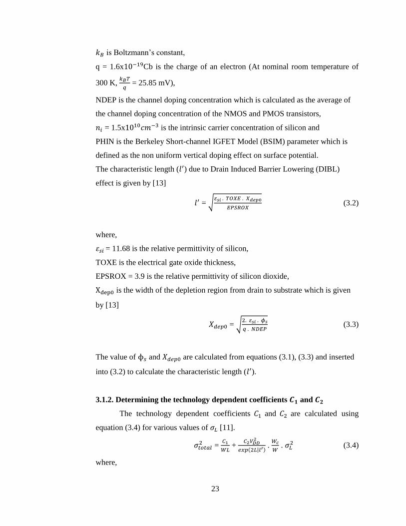
The characteristic length ( ) due to Drain Induced Barrier Lowering (DIBL)
effect is given by [13]
= √
(3.2)
where,
= 11.68 is the relative permittivity of silicon,
TOXE is the electrical gate oxide thickness,
EPSROX = 3.9 is the relative permittivity of silicon dioxide,
is the width of the depletion region from drain to substrate which is given
by [13]
= √
(3.3)
The value of and are calculated from equations (3.1), (3.3) and inserted
into (3.2) to calculate the characteristic length ( ).
3.1.2. Determining the technology dependent coefficients and
The technology dependent coefficients and are calculated using
equation (3.4) for various values of [11].
=
+
( | ) .
.
(3.4)
where,

24
is the variation in ,
W and L are the width and length respectively,
is the supply voltage,
is the correlation length of Line - Edge Roughness (LER),
is the standard deviation in L variation.
From equations (3.1), (3.2), (3.3) and (3.4), the values of , and are
calculated for 22 nm, 32 nm, 45 nm and the 65 nm technology nodes and the
graphs are plotted for each in Figure 3.1.
Figure 3.1 Plot of fitting parameters and
1.15E-18
6.32E-19
6.37E-19
6.44E-19
0.000E+00
0 10 20 30 40 50 60 70
C1 (
V2.m
2)
Technology node (nm)
C1
1.47E+17
5.39E+16
3.60E+16
4.53E+16
0.00E+00
2.00E+16
4.00E+16
6.00E+16
8.00E+16
1.00E+17
1.20E+17
1.40E+17
1.60E+17
0 10 20 30 40 50 60 70
C2 (
V2m
2)
Technology node (nm)
C2

25
From the graphs, it is observed that the values of and are almost the
same for 45 nm and 65 nm technology nodes. Hence the variation in for 90
nm is predicted to be approximately equal to that of the 45 nm and 65 nm
technology nodes.
3.1.3. Extraction of model files with the parameter variations
As now, all the values of the parameters that are to be modified have been
calculated; the next step is to generate the model files with these variations. The
Predictive Technology Model (PTM) [7] is a tool which helps to build the model
files with user defined specifications. It automatically creates the files with the
selected technology nodes and the inputs, including the Slow NMOS and Slow
PMOS design corner (SS), nominal and Fast NMOS and Fast PMOS design
corner (FF) [14]. The files are extracted separately for the NMOS and PMOS
transistors for different nodes (see Appendix C).
The variations in the parameters are set as per Table 3.2 for three standard
deviations which results in the model files for the specified MOSFET.
Table 3.2 Parameter variations in PTM
Technology
node
MOSFET
type
(nm)
Change in
(%)
(V)
Change in
(mv)
(V)
(nm)
(Ω)
32 nm NMOS 20 10 0.21 87.9 1.0 1.3 190
PMOS 20 10 -0.23 87.9 1.0 1.3 240
45 nm NMOS 28 10 0.43 72.9 1.1 1.5 210
PMOS 28 10 -0.49 72.9 1.1 1.5 250
65 nm NMOS 40 10 0.25 60.3 1.2 1.2 165
PMOS 40 10 -0.26 60.3 1.2 1.2 165
90 nm NMOS 56 10 0.23 50.73 1.3 1.4 180
PMOS 56 10 -0.23 50.73 1.3 1.4 200
These individual model files are combined together to calculate the rise time and
the fall time delays.
26
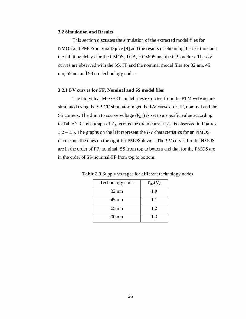
3.2 Simulation and Results
This section discusses the simulation of the extracted model files for
NMOS and PMOS in SmartSpice [9] and the results of obtaining the rise time and
the fall time delays for the CMOS, TGA, HCMOS and the CPL adders. The I-V
curves are observed with the SS, FF and the nominal model files for 32 nm, 45
nm, 65 nm and 90 nm technology nodes.
3.2.1 I-V curves for FF, Nominal and SS model files
The individual MOSFET model files extracted from the PTM website are
simulated using the SPICE simulator to get the I-V curves for FF, nominal and the
SS corners. The drain to source voltage ( ) is set to a specific value according
to Table 3.3 and a graph of versus the drain current ( ) is observed in Figures
3.2 – 3.5. The graphs on the left represent the I-V characteristics for an NMOS
device and the ones on the right for PMOS device. The I-V curves for the NMOS
are in the order of FF, nominal, SS from top to bottom and that for the PMOS are
in the order of SS-nominal-FF from top to bottom.
Table 3.3 Supply voltages for different technology nodes
Technology node (V)
32 nm 1.0
45 nm 1.1
65 nm 1.2
90 nm 1.3

27
Figure 3.2 I-V characteristics for NMOS and PMOS in 32 nm technology node
Figure 3.3 I-V characteristics for NMOS and PMOS in 45 nm technology node
Figure 3.4 I-V characteristics for NMOS and PMOS in 65 nm technology node

28
Figure 3.5 I-V characteristics for NMOS and PMOS in 90 nm technology node
3.2.2 Calculation of Delays
In order to calculate the delays, the netlists are extracted from the physical
layouts containing the FO4 circuit as discussed in section 2.2.3. The drain voltage
( ) is set at = for different technology nodes according to Table 3.3. The
simulations are done with the FF, nominal and SS model files for 32 nm, 45 nm,
65 nm and 90 nm and the corresponding delays and the percentage change in FF
and SS times relative to the nominal are tabulated in Tables 3.4 - 3.7 respectively.
A = % change in the FF relative to Nominal =
(100) (3.5)
B = % change in the SS relative to Nominal =
(100) (3.6)

29
Table 3.4 Rise time and fall time delays in 32 nm technology node
Adder Delay
type
FF
(ps)
Nominal
(ps)
SS
(ps)
A
(%)
B
(%)
CMOS Rise time 90.932 134.84 205.65 32.56 52.51
Fall time 96.839 157.72 268.82 38.60 70.44
TGA Rise time 59.403 102.24 199.31 41.89 94.94
Fall time 54.957 85.264 155.78 35.54 82.70
HCMOS Rise time 110.03 179.94 315.05 38.85 75.08
Fall time 108.44 179.42 331.84 39.56 84.95
CPL Fall time 88.082 183.38 440.8 51.96 140.37
Table 3.5 Rise time and fall time delays in 45 nm technology node
Adder Delay
type
FF
(ps)
Nominal
(ps)
SS
(ps)
A
(%)
B
(%)
CMOS Rise time 206.99 307.64 469.23 32.71 52.52
Fall time 255.75 421.51 836.42 39.32 98.43
TGA Rise time 184.99 317.54 604.92 41.74 90.50
Fall time 143.38 247.66 392.5 42.10 58.48
HCMOS Rise time 279.17 447.67 800.62 37.63 78.84
Fall time 292.23 520.85 975.02 43.89 87.19
CPL Fall time 369.86 692.26 1140.29 46.57 64.72

30
Table 3.6 Rise time and fall time delays in 65 nm technology node.
Adder Delay
type
FF
(ps)
Nominal
(ps)
SS
(ps)
A
(%)
B
(%)
CMOS Rise time 121.02 158.78 212.03 31.20 33.53
Fall time 118.58 169.89 260.46 43.27 53.31
TGA Rise time 81.386 118.28 189.11 31.19 59.88
Fall time 75.971 109.45 137.98 30.58 26.06
HCMOS Rise time 134.65 193.35 263.15 30.35 36.10
Fall time 133.73 191.14 283.44 30.03 48.28
CPL Fall time 138.24 205.31 306.41 32.66 49.24
Table 3.7 Rise time and fall time delays in 90 nm technology node.
Adder Delay
type
FF
(ps)
Nominal
(ps)
SS
(ps)
A
(%)
B
(%)
CMOS Rise time 150.88 189.15 240.36 20.23 27.07
Fall time 151.52 200.45 278.85 24.41 39.11
TGA Rise time 104.19 148.28 193.88 29.73 30.75
Fall time 97.633 130.6 171.2 25.24 31.08
HCMOS Rise time 165.51 226.57 296.48 26.94 30.85
Fall time 179.5 230.56 316.14 22.14 37.11
CPL Fall time 177.44 237.91 340.92 25.41 43.29
As expected, it is observed that the rise time and the fall time delays
increases for the SS corner and decreases for the FF corner. For the CPL adder,
the rise time delay is not critical as it consists of only the NMOS transistors and
there is no pull-up network. The worst case delay will be when the node before
the inverter makes a low to high transition. Therefore, measuring the output after
the inverter means that the emphasis should be on the fall time. The graphs are
plotted for the rise time and the fall time delays from Tables 3.4, 3.5, 3.6 and 3.7
as shown in Figures 3.6 - 3.9.

31
(a)
(b)
Figure 3.6 32 nm technology node (a) Rise time delays (b) Fall time delays
32
(a)
(b)
Figure 3.7 45 nm technology node (a) Rise time delays (b) Fall time delays

33
(a)
(b)
Figure 3.8 65 nm technology node (a) Rise time delays (b) Fall time delays

34
(a)
(b)
Figure 3.9 90 nm technology node (a) Rise time delays (b) Fall time delays
In examining the performance of all the adders with process variations, the TGA
adder has the minimum absolute variance in delay. This is expected since the
TGA adder consistently has the lowest delay of all the adders at all the technology
nodes. It is noteworthy that the CPL and HCMOS adders have a larger increase in
delay when scaled to the 32 nm and simulated with the SS design corner. The
probable reason for this is the dependence on the PMOS feedback to restore the

35
degraded voltage swing at the internal nodes as the pull-up feedback becomes
more ineffective and the maximum signal swing - is reduced.
3.3 Summary
This chapter mainly focuses on the robustness of the adders against
process variation. The method of calculating the change in the threshold voltage
( ) for the 90 nm technology node was discussed. With all the parameter
variation values, the model files for the NMOS and PMOS transistors were
extracted from the PTM website and the I-V characteristics were drawn for the
same. The delays are calculated for CMOS, CPL, TGA and HCMOS adders for
32 nm, 45 nm, 65 nm and 90 nm technology nodes. The TGA and the CMOS
adders performed best with respect to process variations because they have
complementary devices for all signal paths. This ensures that they avoid the
degraded signal swing issue that causes the CPL and HCMOS to experience large
delays when the voltage supply scales down and the threshold voltage increases as
in the SS corner.
36
Chapter Four
Fault Tolerance
As the integrated circuits consists of many transistors on a single chip, it is
essential to test each and every transistor to ensure a fully functional chip. This
chapter discusses the detection of the faults at the output of each adder when
using short and open MOSFET models. The analysis is carried out on the CMOS,
TGA, HCMOS, CPL, 10T and 14T adders. The effect of fault analysis using
testing is also discussed.
4.1 Fault Detection
A single stuck-at MOSFET model is used for the fault analysis. The faults
are classified based on how easy they are to detect and are ranked accordingly. A
graph is plotted to check how the output voltage and the supply current varies
when the FET is shorted with a varying resistance.
4.1.1 Stuck-open and stuck-short faults models
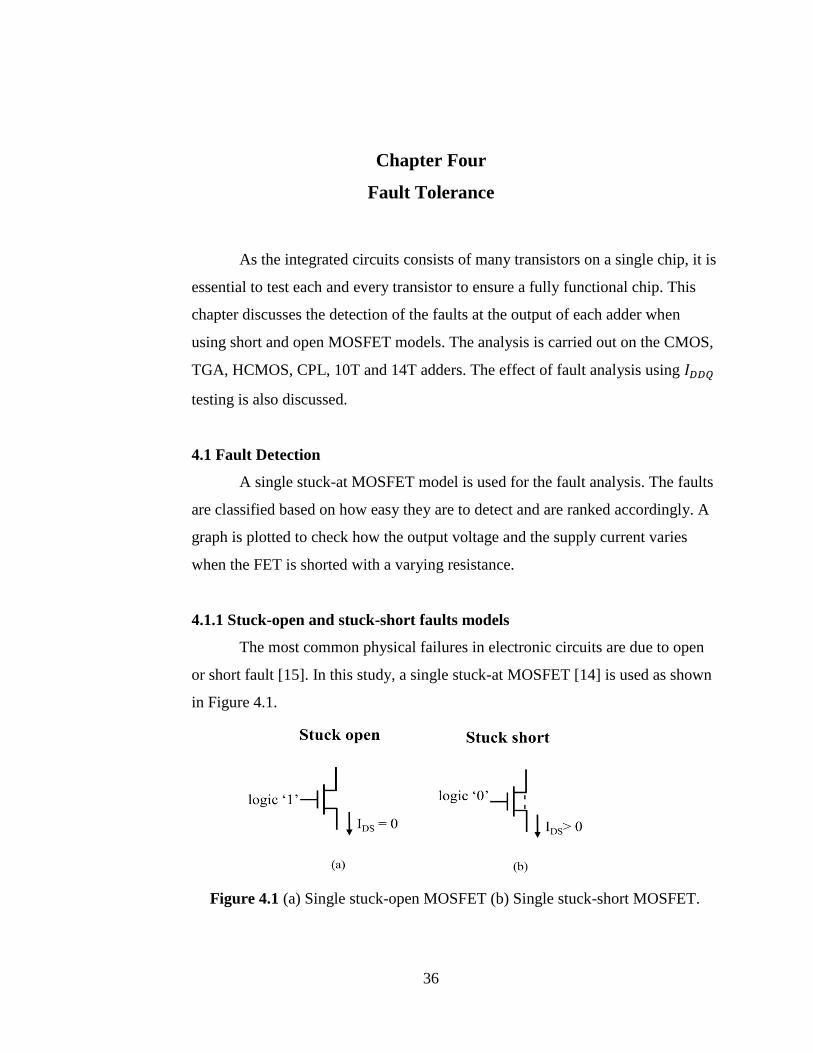
The most common physical failures in electronic circuits are due to open
or short fault [15]. In this study, a single stuck-at MOSFET [14] is used as shown
in Figure 4.1.
Figure 4.1 (a) Single stuck-open MOSFET (b) Single stuck-short MOSFET.

37
When a transistor becomes permanently open due to some physical
defect, a stuck-open fault exists that converts the combinational logic into a
sequential circuit (i.e. the effect of memory is included) which is illustrated in
Figure 4.2 [16]. When A=B=0, the transistors P1, P2 are ON and N1, N2 are OFF
connecting the output (C) to . If a stuck-open fault is introduced at transistor
P1, only P2 is ON and N1, N2 are still OFF which results in a floating output.
There exists some parasitic capacitance ( ) at the output (C) because of previous
operation of circuit. To detect this stuck-open fault, the input vector A=1, B=0 is
first applied to the circuit which discharges the capacitance to ground, yielding a
‘0’ at the output. Then, application of A=B=0 will still yield a ‘0’ at the output
when a ‘1’ is normally expected. Hence, the use of the correct previous state
allows the open fault to be detected with a good grade of fault detection.
The stuck-short fault occurs when the transistor is ON persistently
irrespective of its given input as shown in Figure 4.1 (b). A common cause in
deep submicron technology is a lithography error in the mask alignment, which
causes the drain and the source of the MOS device to be shorted. These two faults
are examined on the transistors and are classified. The detection of the faults is
performed for all the transistors of the adder circuits shown in Figure 4.3 [3].
Figure 4.2 A CMOS NOR circuit.

38

39
Figure 4.3 Circuit schematics of adders (a) CMOS (b) TGA (c) CPL (d)
HCMOS (e) 10T (f) 14T.
4.1.2 Classification of the faults
After the detection of faults, they are classified based on the ease of
detection as shown in Table 4.1. For example, in the strongest case of fault
detection i.e. ‘A’, the output should be 0, but because of the fault it changed from
0 to 1.
The nomenclature below refers to the explanation of the symbols used in
Table 4.1
1 → Strong-‘1’
0 → Strong-‘0’
H → Weak-‘1’ which refers to - as explained in section 2.2.3.
L → Weak-‘0’ which refers to

40
In case of detecting a “weak” fault, a node is driven by conflicting states which
often occurs when a transistor is shorted i.e. “0 vs H” or “1 vs L” and is referred
to as the which is discussed in the following section.
Table 4.1 Classification of faults
Fault Grade Output with error / output
without error
Points
Strong A 1/0 , 0/1 4
Medium strong B L/1 , H/0 3
Weak C (0 vs H (or) 1 vs L)/ 0 (or) 1
(0 vs 1 (or) 1 vs 0)/ 0 (or) 1
2
Very weak D H/L , L/0 , H/1 1
D-
Weak-L/0 0.5
Not detectable F No variation in the output 0
4.1.3 Testing
testing is a part of the integrated circuit testing where the supply
current is monitored to detect a fault. Normally, in a CMOS technology, when the
switching transistors have settled down to the steady state, assuming a minute
leakage current, the static current dissipated by the circuit is almost zero. When a
transistor is shorted, there exists a conduction path from to ground which
results in increased supply current. This increase in the quiescent supply current
can be used to determine if a fault exists. This can be illustrated by using the
circuit in Figure 4.4 [17].
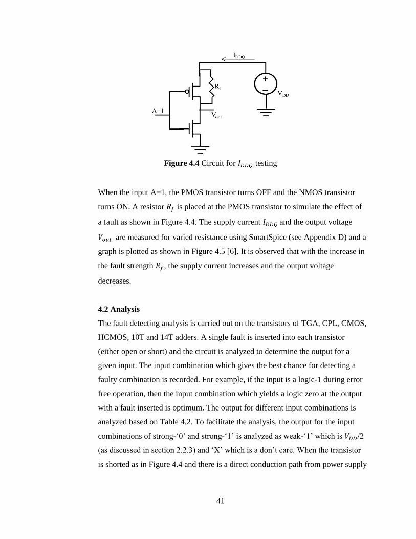
41
Figure 4.4 Circuit for testing
When the input A=1, the PMOS transistor turns OFF and the NMOS transistor
turns ON. A resistor is placed at the PMOS transistor to simulate the effect of
a fault as shown in Figure 4.4. The supply current and the output voltage
are measured for varied resistance using SmartSpice (see Appendix D) and a
graph is plotted as shown in Figure 4.5 [6]. It is observed that with the increase in
the fault strength , the supply current increases and the output voltage
decreases.
4.2 Analysis
The fault detecting analysis is carried out on the transistors of TGA, CPL, CMOS,
HCMOS, 10T and 14T adders. A single fault is inserted into each transistor
(either open or short) and the circuit is analyzed to determine the output for a
given input. The input combination which gives the best chance for detecting a
faulty combination is recorded. For example, if the input is a logic-1 during error
free operation, then the input combination which yields a logic zero at the output
with a fault inserted is optimum. The output for different input combinations is
analyzed based on Table 4.2. To facilitate the analysis, the output for the input
combinations of strong-‘0’ and strong-‘1’ is analyzed as weak-‘1’ which is /2
(as discussed in section 2.2.3) and ‘X’ which is a don’t care. When the transistor
is shorted as in Figure 4.4 and there is a direct conduction path from power supply

42
to ground, then the output is considered to be a weak-‘1’. For each adder, some
special cases are explained in detail.
(a)
(b)
Figure 4.5 Plot of (a) Supply current versus resistance (b) Output voltage versus
resistance.
0
5
10
15
20
25
30
35
40
45
50
0 20 40 60 80 100 120
I DD
Q(u
A)
Rf(KOhm)
IDDQ vs Rf
0
0.2
0.4
0.6
0.8
1
1.2
0 20 40 60 80 100 120
Vo
ut(
V)
Rf(KOhm)
Vout vs Rf

43
Table 4.2 Combination of the inputs and its resulting outputs
1 0 H L
1 1 H/X 1 H
0 H/X 0 L 0
H 1 L H Weak - X
L H 0 Weak - X L
4.2.1 10T
The faults of the 10T full adder are analyzed using the circuit in Figure
4.3(e) and tabulated in Table 4.3.
Table 4.3 Fault detection analysis of 10T full adder
Fault
Transistor
Transistor
Input vector
(A, B, )
Effected
output
Output
with fault
Output
without
fault
Ranking
n5 short (0, 1, 1) Cout 1 vs 0 1 C
p5 short (0, 0, 1) Cout 1 vs 0 0 C
p4 short (0, 0, 0) Sum 1 vs 0 0 C
n4 short (0, 1, 0) Sum 1 vs 0 1 C
p3 short (0, 1, 1) Sum H L D
n3 short (0, 1, 0) Sum H 1 D
p1 short (1, 0, 0) Sum L 1 B
Cout WW1 L D
p2 short (0, 1, 1) Sum WW1 L D
Cout L 1 D
n1 short (0, 0, 0) Sum L 0 D
Cout L 0 D
n2 short (0, 0, 0) Sum L 0 D
Cout L 0 D
n5 open (0, 0, 0) Cout 1 0 A
p5 open (0, 1, 1) Cout 0 1 A

44
Table 4.3 Fault detection analysis of 10T full adder (Continued.)
p4 open (0, 1, 0) Sum 0 1 A
n4 open (0, 0, 0) Sum 1 0 A
p3 open (0, 1, 0) Sum L 1 B
n3 open (0, 1, 1) Sum 1 L B
p1 open (0, 0, 0) Sum 1 0 A
Cout L 0 D
p2 open (0, 0, 0) Sum 1 0 A
Cout L 0 D
n1 open (0, 1, 0) Sum 0 1 A
Cout 0 L D
n2 open (1, 0, 0) Sum 0 1 A
Cout H L D
Consider the case when the transistor p1 is “short”. The fault can be detected when the
input (A, B, ) is (1, 0, 0) as shown in Figure 4.6. As the transistor p1 is short and p2 is
ON, a strong-‘1’ flows through p1 and p2. At the same time, as the transistor n2 is ON, a
strong-‘0’ flows through it and the resulting output at node ‘h’ is considered to be a
weak-‘1’ which is
as mentioned in section 4.2. The weak-‘1’ turns the transistors n4
and n5 partially ON which yields a weak-‘0’ at the sum and weaker-‘1’at the .
Figure 4.6 Fault detection of 10T full adder with transistor p1 “short” and input
(A, B, ) = (1, 0, 0).

45
4.2.2 14T
The analysis of 14T full adder is performed with the circuit in Figure
4.3(f) and the results are tabulated in Table 4.4.
Table 4.4 Fault detection analysis of 14T full adder
Fault
Transistor
Input
vector
(A, B, )
Effected
output
Output with
fault
Output
without
fault
Ranking
n7 short (0, 1, 1) Cout 1 vs 0 1 C
p7 short (1, 0, 0) Cout 0 vs 1 0 C
n6 short (1, 1, 0) Cout 0 vs 1 1 C
p6 short (0, 0, 1) Cout 1 vs 0 0 C
p4 short (0, 1, 1) Sum 1 vs 0 0 C
n4 short (0, 1, 0) Sum 0 vs 1 1 C
p5 short (0, 1, 1) Sum 0 vs 1 0 C
n5 short (1, 0, 0) Sum 0 vs 1 1 C
p3 short (0, 1, 1) Sum WW1 0 B
Cout H vs L 1 C
n3 short (0, 1, 1) Sum H vs 0 0 C
Cout 1 vs WW0 1 C
p1 short (0, 1, 0) Sum H 1 D
Cout L 0 D
p2 short (1, 0, 0) Sum H 1 D
Cout L 0 D
n1 short (0, 0, 0) Sum L 0 D
Cout L 0 D
n2 short (0, 1, 1) Sum L 0 D
Cout H 1 D
n7 open (0, 0, 0) Cout WW0 0 D-
p7 open (1, 1, 0) Cout H 1 D
46
Table 4.4 Fault detection analysis of 14T full adder (Continued.)
n6 open (0, 1, 0) Cout L 0 D
p6 open (0, 1, 1) Cout H 1 D
p5 open (0, 1, 0) Sum 0 1 A
n5 open (0, 1, 1) Sum 1 0 A
n4 open (1, 1, 0) Sum L 0 D
p4 open (0, 0, 1) Sum H 1 D
p3 open (0, 0, 0) Sum WW0 0 D-
Cout L 0 D
n3 open (0, 0, 0) Sum WW0 0 D-
Cout L 0 D
p1 open (1, 0, 0) Sum L 1 B
Cout L vs H 0 C
p2 open (0, 1, 1) Sum H vs L 0 C
Cout H vs L 1 C
n1 open (0, 1, 1) Sum H 0 B
Cout H vs 0 1 C
n2 open (1, 0, 0) Sum 0 vs 1 1 C
Cout 0 vs H 0 C
Consider the case when transistor p1 is “open”. The fault is detected when
the input (A, B, ) is (1, 0, 0) as shown in Figure 4.7. Since the transistors p1
and p2 are OFF, the node ‘x1’ stays in the previous state as discussed in section
4.1.1. For example when (A, B, ) is (0, 0, 1), which results in a weak-‘0’ at the
node ‘x1’. This weak-‘0’ makes the transistor p3 partially ON which allows a
weak-‘1’. The resulting output at node ‘x2’ is a weak-‘0’ which is a combination
of strong-‘0’ and weak-‘1’. The node ‘x1’ makes the transistor p4 partially ON
and results a weak-‘0’ at the “Sum”. The transistors p6 is partially ON through
node ‘x2’and p7 becomes partially ON through node ‘x1’which outputs weak-‘0’
and weak-‘1’ respectively at the .

47
Figure 4.7 Fault detection of 14T full adder with transistor p1 “open” and input
(A, B, ) = (1, 0, 0).
4.2.3 TGA
The fault detection analysis of the TGA full adder is performed with the
circuit of Figure 4.3(b) and the results are tabulated in Table 4.5.
Table 4.5 Fault detection analysis of TGA full adder
Fault
Transistor
Input vector
(A, B, )
Effected
output
Output with
fault
Output
without
fault
Ranking
Mn10 short (0, 1, 1) Cout 1 vs 0 1 C
Mn9 short (1, 1, 0) Cout 0 vs 1 1 C
Mp10 short (1, 0, 0) Cout 0 vs 1 0 C
Mp9 short (0, 0, 1) Cout 1 vs 0 0 C
Mp6 short (0, 1, 1) Sum 1 vs 0 0 C
Mn6 short (0, 1, 0) Sum 0 vs 1 1 C
Mp7 short (0, 0, 0) Sum 0 vs 1 0 C
Mn7 short (0, 0, 1) Sum 1 vs 0 1 C
Mp5 short (0, 1, 1) Sum H 0 C
Mn5 short (0, 1, 0) Sum H 1 C

48
Table 4.5 Fault detection analysis of TGA full adder (Continued.)
Mp8 short (0, 1, 0) Sum L vs H 1 C
Cout 0 vs L 0 C
Mn8 short (0, 0, 0) Sum L 0 C
Cout L 0 C
Mp1 short (1, 1, 0) Sum L 0 C
Cout H 1 C
Mn1 short (0, 0, 1) Sum H 1 C
Cout L 0 C
Mp3 short (1, 1, 0) Sum H 0 C
Cout L 1 C
Mn3 short (0, 1, 0) Sum H 1 C
Cout L 0 C
Mp2 short1 (1, 1, 0) Sum H 0 D
Cout L 1 D
Mn2 short (1, 1, 0) Sum L 0 D
Cout H 1 D
Mp4 short1 (1, 0, 0) Sum H 1 D
Cout L 0 D
Mn4 short (0, 0, 0) Sum L 0 D
Cout L 0 D
Mp10 open (1, 1, 0) Cout H 1 D
Mn10 open (0, 0, 0) Cout L 0 D
Mn9 open (0, 1, 0) Cout L 0 D
Mp9 open (0, 1, 1) Cout H 1 D
Mp6 open (0, 0, 1) Sum H 1 D
Mn6 open (0, 0, 0) Sum L 0 D
Mp7 open (0, 1, 0) Sum H 1 D
Mn7 open (0, 1, 1) Sum L 0 D
Mp5 open (0, 1, 0) Sum 0 1 A

49
Table 4.5 Fault detection analysis of TGA full adder (Continued.)
Mn5 open (0, 1, 1) Sum 1 0 A
Mp8 open (1, 1, 0) Sum L vs 1 0 C
Cout L vs 1 1 C
Mn8 open (1, 0, 0) sum 0 vs H 1 C
Cout 0 vs H 0 C
Mp1 open (0, 0, 1) Sum L 1 B
Cout H 0 B
Mn1 open (0, 1, 1) Sum H 0 B
Cout L 1 B
Mp3 open (0, 1, 1) Sum 1 0 A
Cout 0 1 A
Mn3 open (1, 1, 0) Sum 1 0 A
Cout 0 1 A
Mp2 open (1, 0, 0) Sum H 1 D
Cout L 0 D
Mn2 open (0, 0, 1) Sum H 1 D
Cout L 0 D
Mp4 open (0, 1, 0) Sum H 1 D
Cout L 0 D
Mn4 open (1, 1, 0) Sum L 0 D
Cout H 1 D
1Note: These are two special cases due to asymmetry as mentioned in section 4.2.
Consider the case when Mp5 is “short” as shown in Figure 4.8. The analysis can
be performed when the input (A, B, ) is (0, 1, 1). This fault can be detected
through testing which is discussed in section 4.1.3 as both the transistors
Mp5 and Mn5 are ON. The output of these two transistors will be a weak-‘1’ as
discussed in section 4.2, which results at the “Sum” as the transistor Mp7 is ON.

50
Figure 4.8 Fault detection of TGA full adder with transistor Mp5 “short” and
input (A, B, ) = (0, 1, 1).
In the analysis of TGA full adder, when the transistors Mp5, Mn5, Mp8, Mn8,
Mp1, Mn1, Mp3 and Mn3 are short, this fault can be detected through
testing as discussed in section 4.1.3 and the resulting output is ranked ‘C’.
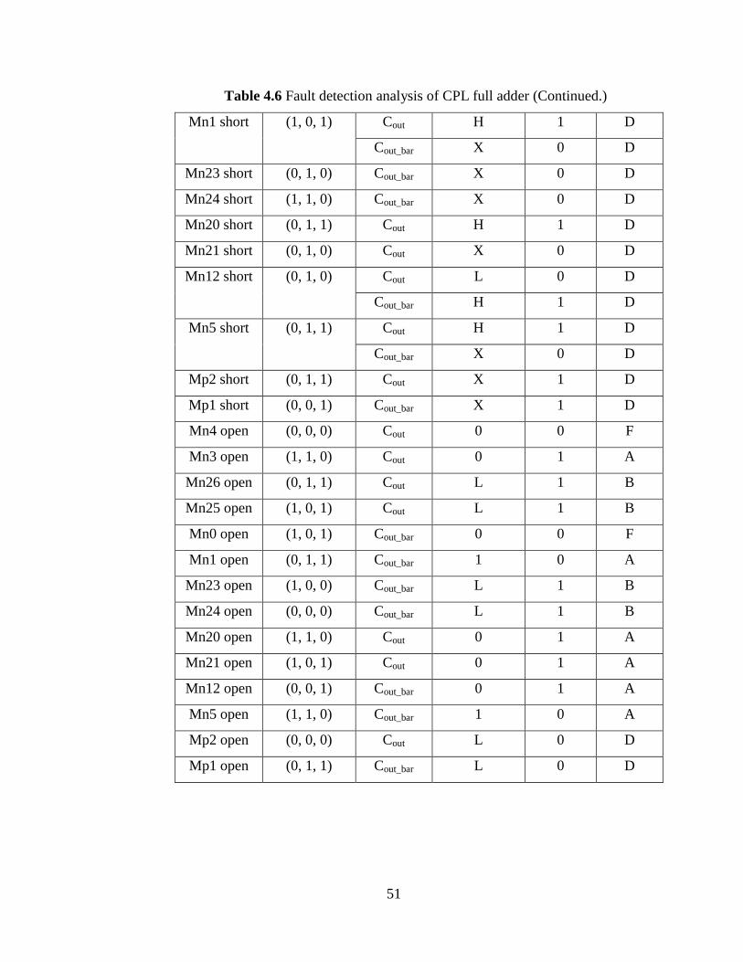
4.2.4 CPL
The faults of the CPL full adder are analyzed using the circuit in Figure
4.3(c) and tabulated in Table 4.6.
Table 4.6 Fault detection analysis of CPL full adder,
Fault
Transistor
Input vector
(A, B, )
Effected
output
Output with
fault
Output
without
fault
Ranking
Mn4 short (1, 1, 0) Cout H 1 D
Mn3 short (0, 1, 0) Cout X 0 D
Mn26 short (1, 0, 1) Cout H 1 D
Mn25 short (0, 0, 1) Cout X 0 D
Mn0 short (0, 0, 1) Cout L 0 D
Cout_bar H 1 D
51
Table 4.6 Fault detection analysis of CPL full adder (Continued.)
Mn1 short (1, 0, 1) Cout H 1 D
Cout_bar X 0 D
Mn23 short (0, 1, 0) Cout_bar X 0 D
Mn24 short (1, 1, 0) Cout_bar X 0 D
Mn20 short (0, 1, 1) Cout H 1 D
Mn21 short (0, 1, 0) Cout X 0 D
Mn12 short (0, 1, 0) Cout L 0 D
Cout_bar H 1 D
Mn5 short (0, 1, 1) Cout H 1 D
Cout_bar X 0 D
Mp2 short (0, 1, 1) Cout X 1 D
Mp1 short (0, 0, 1) Cout_bar X 1 D
Mn4 open (0, 0, 0) Cout 0 0 F
Mn3 open (1, 1, 0) Cout 0 1 A
Mn26 open (0, 1, 1) Cout L 1 B
Mn25 open (1, 0, 1) Cout L 1 B
Mn0 open (1, 0, 1) Cout_bar 0 0 F
Mn1 open (0, 1, 1) Cout_bar 1 0 A
Mn23 open (1, 0, 0) Cout_bar L 1 B
Mn24 open (0, 0, 0) Cout_bar L 1 B
Mn20 open (1, 1, 0) Cout 0 1 A
Mn21 open (1, 0, 1) Cout 0 1 A
Mn12 open (0, 0, 1) Cout_bar 0 1 A
Mn5 open (1, 1, 0) Cout_bar 1 0 A
Mp2 open (0, 0, 0) Cout L 0 D
Mp1 open (0, 1, 1) Cout_bar L 0 D

52
Table 4.6 Fault detection analysis of CPL full adder (Continued.)
Fault
Transistor
Input vector
(A, B, )
Effected
output
Output with
fault
Output
without
fault
Ranking
Mn9 short (1, 0, 0) Sum H 1 D
Mn6 short (0, 1, 0) Sum H 1 D
Mn7 short (1, 1, 1) Sum H 1 D
Mn8 short (0, 0, 1) Sum H 1 D
Mn10 short (0, 0, 1) Sum H 1 D
Mn11 short (0, 1, 0) Sum H 1 D
Mn14 short (1, 1, 0) Sum L 0 D
Sum_bar H 1 D
Mn13 short (1, 0, 1) Sum L 0 D
Sum_bar H 1 D
Mp4 short (0, 0, 1) Sum H 1 D
Mp3 short (0, 1, 1) Sum L 0 D
Sum_bar H 1 D
Mn9 open (0, 1, 0) Sum L 1 B
Mn6 open (1, 0, 0) Sum L 1 B
Mn7 open (0, 0, 1) Sum L 1 B
Mn8 open (1, 1, 1) Sum L 1 B
Mn10 open (0, 0, 0) Sum H 0 B
Mn11 open (0, 0, 1) Sum L 1 B
Mn14 open (0, 1, 1) Sum L 0 D
Sum_bar 0 1 A
Mn13 open (0, 0, 0) Sum L 0 D
Sum_bar 0 1 A
Mp4 open (0, 0, 0) Sum L 0 D
Mp3 open (0, 0, 1) Sum_bar L 0 D

53
When the transistor Mn3 is “short”, the fault is detected when the input
(A, B, ) is (0, 1, 0) as shown in Figure 4.9. As the NMOS transistor passes a
strong-‘0’, the output of the transistor Mn3 is a strong-‘0’. This combines with the
weak-‘1’ which is the output of the transistor Mn4 and results a weak-‘0’. As the
transistor Mn20 is ON, the weak-‘0’ pass through it. Even though the transistor
P2 is ON, a weak-‘1’ passes through it because of its small size. Now the outputs
of Mn20 and P2 results in an ‘X’ at the which is a combination of weak-‘0’
and weak’1’ respectively. So the resulting output of is also an ‘X’ which is
an inversion of .
Figure 4.9 Fault detection of CPL full adder with transistor Mn3 “short” and
input (A, B, ) = (0, 1, 0).
When the transistor Mn4 is “open”, the fault detection is analyzed when
the input (A, B, ) is (0, 0, 0) as shown in Figure 4.10. Since the transistors Mn3
and Mn4 are OFF, the previous state holds at the output of Mn4 drain, which is
strong-‘0’ when the input is (1, 1, 1). Because of the capacitance at the output of
transistors Mn3 and Mn4, its output becomes a slow-‘0’ instead of strong-‘0’.
Therefore, the output of the transistor Mn20 is driven by the transistor P2 which is

54
ON and results a slow-‘1’ at . So, the result at is a ‘0’ which is the
inversion of .
Figure 4.10 Fault detection of CPL full adder with transistor Mn4 “open” and
input (A, B, ) = (0, 0, 0).
4.2.5 Static CMOS
The fault detection of the static CMOS full adder is performed with the
circuit of Figure 4.3(a) and the results are tabulated in Table 4.7.
Table 4.7 Fault detection analysis of static CMOS full adder
Fault
Transistor
Input vector
(A, B, )
Effected
output
Output with
fault
Output
without
fault
Ranking
Mn3 short (0, 1, 0) Cout 0 vs 1 0 C
Sum X 1 C
Mp3 short (0, 1, 1) Cout 1 vs 0 1 C
Sum X 0 C
Mn1 short (0, 0, 1) Cout 0 vs 1 0 C
Sum X 1 C

55
Table 4.7 Fault detection analysis of static CMOS full adder (Continued.)
Mp1 short (1, 1, 0) Cout 1 vs 0 1 C
Sum X 0 C
Mn2 short (0, 0, 1) Cout 0 vs 1 0 C
Sum X 1 C
Mp2 short (1, 1, 0) Cout 1 vs 0 1 C
Sum X 0 C
Mn4 short (0, 1, 0) Cout 0 vs 1 0 C
Sum X 1 C
Mp4 short (1, 0, 1) Cout 1 vs 0 1 C
Sum X 0 C
Mn5 short (1, 0, 0) Cout 0 vs 1 0 C
Sum X 1 C
Mp5 short (0, 1, 1) Cout 1 vs 0 1 C
Sum X 0 C
Mn6 short (0, 0, 0) Sum 0 vs 1 0 C
Mp6 short (1, 1, 1) Sum X 1 C
Mn7 short (0, 0, 0) Sum 0 vs 1 0 C
Mp7 short (1, 1, 1) Sum X 1 C
Mn8 short (0, 0, 0) Sum 0 vs 1 0 C
Mp8 short (1, 1, 1) Sum X 1 C
Mp9 short (0, 0, 1) Sum 1 vs 0 1 C
Mn9 short (0, 1, 1) Sum 0 vs 1 0 C
Mn10 short (0, 1, 1) Sum 0 vs 1 0 C
Mp10 short (1, 0, 0) Sum 1 vs 0 1 C
Mn11 short (1, 0, 1) Sum 0 vs 1 0 C
Mp11 short (0, 1, 0) Sum 1 vs 0 1 C
Mn12 short (1, 1, 0) Sum 0 vs 1 0 C
Mp12 short (0, 0, 1) Sum 1 vs 0 1 C
Mn1 open (1, 0, 1) Cout 0 1 A
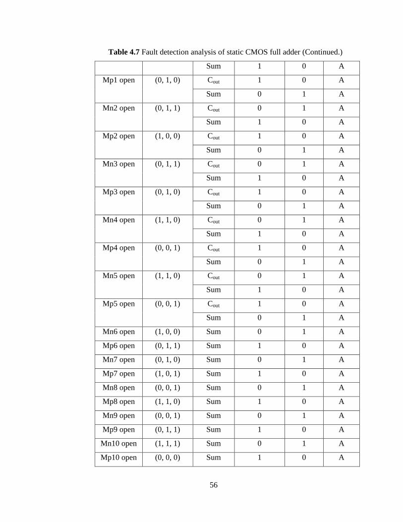
56
Table 4.7 Fault detection analysis of static CMOS full adder (Continued.)
Sum 1 0 A
Mp1 open (0, 1, 0) Cout 1 0 A
Sum 0 1 A
Mn2 open (0, 1, 1) Cout 0 1 A
Sum 1 0 A
Mp2 open (1, 0, 0) Cout 1 0 A
Sum 0 1 A
Mn3 open (0, 1, 1) Cout 0 1 A
Sum 1 0 A
Mp3 open (0, 1, 0) Cout 1 0 A
Sum 0 1 A
Mn4 open (1, 1, 0) Cout 0 1 A
Sum 1 0 A
Mp4 open (0, 0, 1) Cout 1 0 A
Sum 0 1 A
Mn5 open (1, 1, 0) Cout 0 1 A
Sum 1 0 A
Mp5 open (0, 0, 1) Cout 1 0 A
Sum 0 1 A
Mn6 open (1, 0, 0) Sum 0 1 A
Mp6 open (0, 1, 1) Sum 1 0 A
Mn7 open (0, 1, 0) Sum 0 1 A
Mp7 open (1, 0, 1) Sum 1 0 A
Mn8 open (0, 0, 1) Sum 0 1 A
Mp8 open (1, 1, 0) Sum 1 0 A
Mn9 open (0, 0, 1) Sum 0 1 A
Mp9 open (0, 1, 1) Sum 1 0 A
Mn10 open (1, 1, 1) Sum 0 1 A
Mp10 open (0, 0, 0) Sum 1 0 A

57
Table 4.7 Fault detection analysis of static CMOS full adder (Continued.)
Mn11 open (1, 1, 0) Sum 1 0 A
Mp11 open (1, 0, 0) Sum 0 1 A
Mn12 open (1, 0, 1) Sum 1 0 A
Mp12 open (1, 0, 0) Sum 0 1 A
When the transistor Mp6 is “short”, the fault is detected when the input (A, B,
) is (1, 1, 1) as shown in Figure 4.11. Since the transistors Mp6 and Mp9 are
ON, the output at the transistor Mp9 is a strong-‘1’. The strong-‘1’ combines with
the strong-‘0’ at the input of the inverter with the transistors Mp13, Mp14 and
results an unknown state ‘X’. So the output at the “Sum” will be an ‘X’ which is
the inversion of the input of inverter.
Figure 4.11 Fault detection of static CMOS full adder with transistor Mp6 “short”
and input (A, B, ) = (1, 1, 1).
4.2.6 HCMOS
The faults of the HCMOS full adder are analyzed using the circuit in
Figure 4.3(d) and tabulated in Table 4.8.

58
Table 4.8 Fault detection analysis of HCMOS full adder
Fault
Transistor
Input vector
(A, B, )
Effected
output
Output with
fault
Output
without
fault
Ranking
N13 short (0, 1, 0) Cout 0 vs 1 0 C
N12 short (1, 0, 0) Cout 0 vs 1 0 C
P13 short (1, 0, 1) Cout 1 vs 0 1 C
P12 short (0, 1, 1) Cout 1 vs 0 1 C
N11 short (0, 0, 0) Sum 0 vs 1 0 C
P11 short (0, 0, 1) Sum 1 vs 0 1 C
N10 short (0, 0, 1) Cout 0 vs 1 0 C
P10 short (1, 1, 0) Cout 1 vs 0 1 C
N9 short (0, 0, 1) Sum 1 vs 0 1 C
N8 short (0, 0, 1) Sum 1 vs 0 1 C
N7 short (1, 0, 0) Cout 0 vs L 0 F
Sum 1 vs H 1 F
N6 short (1, 0, 0) Cout 0 vs L 0 F
Sum 1 vs H 1 F
P7 short (0, 1, 0) Cout L 0 D
Sum 1 1 F
P6 short (1, 1, 0) Cout H 1 D
Sum 0 0 F
N3 short (0, 1, 0) Cout 0 vs 1 0 C
P3 short (0, 1, 1) Cout 1 vs 0 1 C
N2 short (0, 0, 0) Sum 0 vs 1 0 C
P2 short (0, 0, 1) Sum 1 vs 0 1 C
N1 short (0, 0, 0) Sum 0 vs L 0 F
P1 short (1, 1, 0) Sum 0 vs L 0 F

59
Table 4.8 Fault detection analysis of HCMOS full adder (Continued.)
N13 open (1, 1, 0) Cout 0 1 A
P13 open (0, 0, 0) Cout 1 0 A
N12 open (1, 1, 0) Cout 0 1 A
P12 open (0, 0, 0) Cout 1 0 A
N11 open (0, 0, 1) Sum 0 1 A
P11 open (0, 0, 0) Sum 1 0 A
N10 open (0, 1, 1) Cout H 1 D
P10 open (0, 1, 0) Cout L 0 D
N9 open (1, 0, 0) Cout 1 0 A
Sum 0 1 A
N8 open (0, 1, 1) Cout H 1 D
Sum L 0 D
N7 open (1, 1, 0) Cout H 1 D
Sum L 0 D
N6 open (0, 0, 0) Sum 1 0 A
P7 open (1, 1, 0) Cout 1 vs 0 1 C
Sum H 0 B
P6 open (1, 0, 1) Cout H 1 D
Sum 0 vs 1 0 C
N3 open (0, 1, 1) Cout 0 1 A
P3 open (0, 1, 0) Cout 1 0 A
N2 open (0, 1, 0) Sum H 1 D
P2 open (0, 1, 1) Sum L 0 D
N1 open (1, 0, 1) Cout H 1 D
P1 open (0, 1, 1) Cout 0 1 A
Sum 1 0 A

60
When the transistor P10 is “open”, the fault is detected when the input (A, B, )
is (0, 1, 0) as shown in Figure 4.12. The transistor N10 passes a weak-‘1’ which
results at the . So the output of the inverter is a weak-‘0’ at .
Figure 4.12 Fault detection of HCMOS full adder with transistor P10 “open” and
input (A, B, ) = (0, 1, 0).
4.3 Discussion
This section discusses the overall grading of each full adder as tabulated in
Table 4.9. The final grade is calculated by taking Table 4.1 into consideration.
Table 4.9 Overall grading of full adder designs
Full adder Grade
10T 2.7
14T 1.8
TGA 1.85
CPL 1.87
Static CMOS 3
HCMOS 2.15

61
10T: The final grade of the 10T full adder is calculated as a good grade of
2.7. This is because when the transistors are “open”, the fault strength is ‘A’
(8/10) or ‘B’ (2/10) and when the transistors are “short”, it is either ‘C’ or ‘D’.
There is no duality at the output and it uses memory effectively. Also there is a
single path for each logic state.
14T: The overall grade of the 14T full adder is 1.8. In the 14T adder, there
exists a duality at the output (i.e., a CMOS transmission gate consisting of a pair
of nMOS and pMOS devices) which results in conflicting states when the
transistors are “short” and the fault strengths are either ‘C’ or ‘D’. The feedback
prevents the effective use of previous state memory for detecting faults and many
of the “open” cases are either ‘C’ or ‘D’.
TGA: The final grade of the TGA full adder is 1.85. Duality exists
throughout the TGA adder. When the transistors are “short”, the output is
considered as /2 which gives an unknown state ‘X’ or a weak-‘1’ and the fault
strength is classified as either ‘C’ or ‘D’. There are two special cases when the
transistors Mp4 and Mp2 are short and the fault strength is a ‘D’ (for this case,
/2 is considered as the unknown state ‘X’ rather than weak-‘1’ to avoid giving
this fault condition an artificially high grade of B and to avoid asymmetry with
the case where the corresponding n-channel devices are shorted). When the
transistors are “open”, the memory is ineffective because of duality except when
the transistors Mp3 and Mn3 are open, and the fault strength of these two
transistors is A.
CPL: The overall grade of the CPL full adder is calculated as 1.87. The
memory is ineffective due to the presence of the weak PMOS pull-ups (transistors
P3 and P4). When the transistors are “short”, all of them produce a fault strength
of ‘D’. This is because there occurs a conflict with PMOS pull-ups as analyzed in
the example in section 4.2.4 with the transistor Mn3 “short” which yields an
unknown state ‘X’ at the output. Also, the node is driven to conflicting states. For
example, when the transistor Mn4 is short which yields ‘D’ at the output. In case
of the transistors being “open”, most of the cases are either ‘A’ or ‘B’. Here, two
outputs i.e. and are analyzed. Usually a case is found where the

62
pull-up transistors P1 or P2 are OFF and therefore the memory works effectively
detecting the faults. Only in the case when the transistors Mn4 or Mn0 are “open”,
the fault strength is ‘F’ since they are always connected to ‘1’.
Static CMOS: The final grade of the static CMOS full adder is 3. When
the transistors are “open”, all of them yields fault strength of ‘A’ because the
CMOS adder is fully complementary. This implies that the memory always works
as the previous state always yields an output which is the opposite of the expected
value output under fault-free operation. When the transistors are “short”, all of
them yields fault strength of ‘C’. This is because if there is “short” in one tree (for
example, the PMOS transistors), then the NMOS tree will be ON and conflicting
states occur which results in an unknown state ‘X’ and is ranked ‘C’.
HCMOS: The final grade of the HCMOS full adder is 2.15. When the
transistors are “short”, all of them yield fault strength of either “C” or “D” or “F”.
The transistors P6 and P7 lead to conflicts in “Module 1”. Also the transistor pairs
N6, N7 and N8, N9 lead to conflicts because of cross coupling. This may occur
because of the conflicts between PMOS pull ups or the nodes driving to the
conflicting states as discussed for CPL above. In “Module 2” and “Module 3”,
there are transmission gates which also have the problems when the transistors are
“short” as explained for TGA above. In case the transistors are “open”, “Module
2” and “Module 3” cannot use the previous state because of the transmission gates
P10, N10 and P2, N2. The transmission gates P2, N2 or P3, N3 give alternate
paths and so the previous state in “Module 1” is overridden. So “Module 1” is
similar to the CPL with previous state but as it drives the CMOS transmission
gate, it does not work.
4.4 Summary
The stuck-open and stuck-short faults are analyzed for all the transistors of
static CMOS, TGA, CPL, HCMOS, 10T and 14T full adders and are ranked based
on the fault strength. In the 14T and the CPL adders, because of feedback, they
cannot use the previous state effectively to detect the faults. Static CMOS has the
best fault detectability because its complementary logic trees allow the previous

63
memory state to be used effectively for detecting faults. The lack of
complementary signal paths (no duality) in the 10T allows it to make effective use
of memory as well to achieve a good fault detectability rating. Therefore, based
on the analysis of the adders studied in this thesis, it is concluded that effective
use of the memory state in the open MOSFET case is the key to obtaining a good
fault detectability grade.

64
Chapter 5
Conclusion and Future work
5.1 Conclusion
The objective of this research was to implement the low transistor count
10T and 14T full adders and compare them with the TGA and static CMOS
adders. The key process parameters were identified and varied to find how robust
the various adders are to process variations. The fault detectability of the full
adders was also analyzed.
The 10T and 14T full adders were implemented and the physical layouts
were drawn using the Electric layout design tool. The extracted netlist was
simulated using SmartSpice to determine the delay for different capacitive loads
and the variation in supply voltages and to calculate the power dissipation. The
primary process variation parameters were identified to determine the robustness
of various adders and the delays were calculated with the FF, nominal and SS
model files. The stuck-open and stuck-short faults were analyzed on all the
transistors of CMOS, CPL, TGA, HCMOS, 10T and 14T full adders and were
ranked based on the ease of fault detection.
From the results, it is observed that the 10T and 14T adders do not scale
well with the technology nodes due to the requirement for very low power
supplies. So, the simulations were performed only on the 90 nm technology node.
With the delay versus capacitive load, the 14T adder performs better compared to
static CMOS because in most of the cases the input signal must propagate through
a single transmission gate to reach the output. The 10T adder has a single PMOS
or NMOS path to the output resulting in degraded voltage swing at both the
internal nodes and the output in many cases. Hence the 10T adder has the worst
load versus delay characteristics for large capacitive loads. The 14T full adder
dissipated low power compared to the TGA and static CMOS adders as its voltage
swings ranged from 0 and - and not between 0 and as seen in the TGA

65
and CMOS adders. With the change in process variations, the TGA adder has the
minimum absolute variance in delay. The CPL and HCMOS adders have a larger
increase in delay when scaled to the 32 nm and simulated with the SS design
corner.
In conclusion, the main contribution of this thesis is the specification of
guidelines for obtaining optimum performance of adder circuits implemented in
nanoscale technologies. First, due to the reduced supply voltages required for
deep submicron processes, it is important that all signal paths have the proper
FETs for passing the required signals (i.e., a logic – ‘1’ should be passed by a
pMOS device and a logic – ‘0’ by an nMOS transistor). Second, the use of
feedback circuits to restore the degraded signal swings should be avoided. Third,
to ensure good driving capability and minimal delay, the output signals should be
buffered or have a minimum number of pass-gates connecting the input of the
gate to its output. The above criteria are consistent with the overall conclusion
that the TGA and static CMOS adders are the most promising candidates for
implementing adders in nanoscale technologies.
5.2 Future work
The work presented in this thesis can be extended further. First, the
analysis of the adders for fault detection can be enhanced by analyzing the adders
for multiple faults. To carry out this analysis, a fault simulation tool should be
built that can handle the varying logic levels that occur within the adder circuits
(such as weak-0 and weak-1) and the feedback mechanisms that are utilized in the
CPL and HCMOS adders. Second, the various adder circuits that were studied in
this thesis should be evaluated for use in the emerging nanotechnologies, such as
Carbon Nanotube Transistors (CNTs) and nanowire Field Effect Transistors
(FET) processes. In particular, the implementation of pass-transistor logic
families should be considered using CNTs. While pass-transistor logic has the
advantage of a more compact logic network compared to static CMOS, this study
has found that the adders which use this logic family, such as the CPL and
HCMOS, experience scalability problems when low voltage supplies are utilized.

66
It would be interesting to see if similar issues occur with CNT technologies and
how they can be optimized.
67
References
[1] Gartner Newsroom: http://www.gartner.com/it/page.jsp?id=1372013
[2] mobi Thinking: http://mobithinking.com/mobile-marketing-tools/latest-
mobile-stats
[3] Chip-Hong Chang, Jiangmin Gu, Mingyan Zhang, “A Review of 0.18-um
Full adder Performances for Tree Structured Arithmetic Circuits,” IEEE
Transactions on Very Large Scale Integration (VLSI) Systems, vol. 13, no.
6, pp. 686-695, June 2005.
[4] S. Goel, A. Kumar, M. A. Bayoumi, “Design of Robust, Energy-Efficient
Full Adders for Deep-Submicrometer Design Using Hybrid-CMOS Logic
Style,” IEEE Transactions on Very Large Scale Integration (VLSI)
Systems, vol. 14, no. 12, pp. 1309-1321, Dec. 2006.
[5] Wei Zhao, Frank Liu, Kanak Agarwal, Dhruva Acharya, Sani R. Nassif,
Kevin J. Nowka, Yu Cao, “Rigorous Extraction of Process Variations for
65-nm CMOS Design,” IEEE Transactions on Semiconductor
Manufacturing, vol. 22, no. 1, pp. 196-203, February 2009.
[6] M. Faisal, A. Hasib, A. B. M. H. Rashid, “Fault characterisation and
testability issues of complementary pass transistor logic circuits,” IEE
Proceedings on Circuits, Devices and Systems, vol. 152, no. 3, pp. 215-
222, June 2005.
[7] Predictive Technology Model: http://ptm.asu.edu/
[8] Rahul Jesuran Gera, “Analysis of Adder Circuits in Deep Submicron
Technologies,” MSEE Thesis, The University of Texas at Tyler, August
2011.
[9] SIMUCAD SmartSpice User’s Manual – Volume 1 and Volume 2,
Simucad Design Automation, Inc. January 2008.

68
[10] S. M. Kang and Y. Leblebci, CMOS Digital Integrated Circuits: Analysis
and Design. McGraw-Hill Companies, Third edition, 2003.
[11] Yun Ye, Frank Liu, Min Chen, Sani Nassif, Yu Cao, ”Statistical Modeling
and Simulation of Threshold Variation Under Random Dopant
Fluctuations and Line-edge Roughness,” IEEE Transactions on Very
Large Scale Integration (VLSI) Systems, vol. 19, no. 6, pp. 987-996, June
2011.
[12] International Technology Roadmap for Semiconductors:
http://www.itrs.net/
[13] Nahushabha Bhadravati Mohankumar, “An Ultra Wide Band CMOS Low
Noise Amplifier Design,” MSEE Thesis, The University of Texas at
Arlington, December 2010.
[14] Neil H. E. Weste and David Money Harris, CMOS VLSI Design: A
Circuits and Systems Perspective. Addison – Wesley, Fourth Edition,
2011.
[15] Prithviraj Kabisatpathy, Alok Barua, Satyabroto Sinha, “Fault Diagnosis
of Analog Integrated Circuits,” Springer Publishers, 2005.
[16] Michael L. Bushnell, Vishwani D. Agrawal, “Essentials of Electronic
Testing For Digital, Memory and Mixed-Signal VLSI Circuits,” Kluwer
Academic Publishers, 2000.
[17] Rajsuman, R., “Iddq testing for CMOS VLSI,” Proceedings of the IEEE,
vol. 88, no. 4, pp. 544-568, Apr 2000.

69
Appendix A: Worst Case Calculations
1. 10T full adder worst case calculations figure
Figure A.1 Worst case paths for 10T full adder
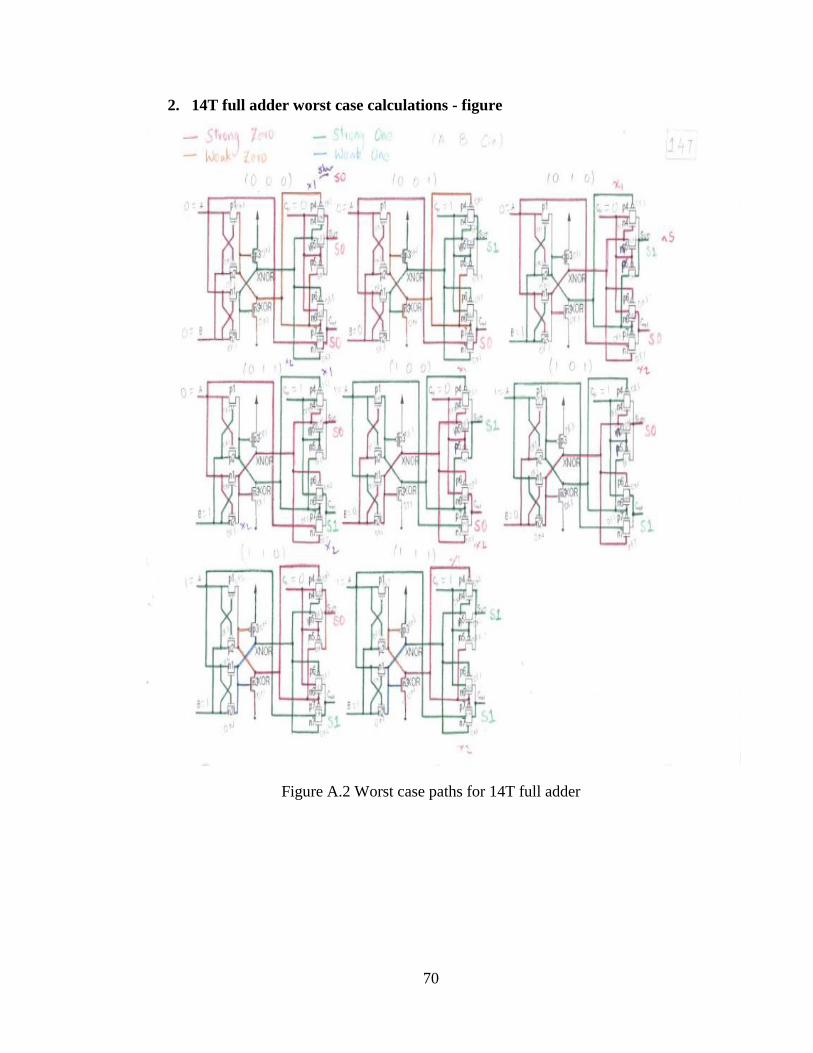
70
2. 14T full adder worst case calculations - figure
Figure A.2 Worst case paths for 14T full adder

71
Appendix B: SPICE netlist for 10T and 14T full adders
1. 10T adder with capacitive load at output
.include /home/student/Desktop/RESEARCH/Model_Files/90nm_LP_pm-1.txt
.Param Vx=1.3V Vl=0V Vh=1.3V
+tr=20p tf=20p trf=10p td=3n tph=3*td
+ta1=td-trf ta2=ta1+tr ta3=ta2+td-tr ta4=ta3+tf ta5=ta4+td-tr
ta6=ta5+tr ta7=ta6+2*td-tr ta8=ta7+tf ta9=ta8+tph-tr ta10=ta9+tr
ta11=ta10+td-tr
+tb1=td-trf tb2=tb1+tr tb3=tb2+tph-tr tb4=tb3+tf tb5=tb4+2*td-tr
tb6=tb5+tr tb7=tb6+td-tr tb8=tb7+tf tb9=tb8+2*td-tr
+tc1=tph-trf tc2=tc1+tr tc3=tc2+td-tr tc4=tc3+tf tc5=tc4+2*td-tr
tc6=tc5+tr tc7=tc6+tph-tr
Mn1 h B A gnd N L=0.09U W=0.18U AS=0.115P AD=0.053P PS=1.485U
PD=0.81U
Mn2 B A h gnd N L=0.09U W=0.18U AS=0.053P AD=0.138P PS=0.81U
PD=1.68U
Mn3 h Cin i gnd N L=0.09U W=0.18U AS=0.081P AD=0.053P PS=1.14U
PD=0.81U
Mn4 Sum h Cin gnd N L=0.09U W=0.18U AS=0.128P AD=0.073P PS=1.575U
PD=1.08U
Mn5 Cout h A gnd N L=0.09U W=0.18U AS=0.115P AD=0.073P PS=1.485U
PD=1.08U
Mnmos@0 A Inv_A_1 Gnd gnd N L=0.09U W=0.54U AS=0.081P AD=0.115P
PS=1.17U
+PD=1.485U
Mnmos@1 Inv_A_1 A_1 Gnd gnd N L=0.09U W=0.18U AS=0.081P
AD=0.061P PS=1.17U
+PD=0.99U
Mnmos@2 Cin Inv_Cin_1 Gnd gnd N L=0.09U W=0.54U AS=0.081P
AD=0.128P PS=1.17U
+PD=1.575U
Mnmos@3 Inv_Cin_1 Cin_1 Gnd gnd N L=0.09U W=0.18U AS=0.081P
AD=0.061P
+PS=1.17U PD=0.99U
Mnmos@4 Gnd Inv_B_1 B gnd N L=0.09U W=0.54U AS=0.138P AD=0.081P
PS=1.68U
+PD=1.17U
Mnmos@5 Gnd B_1 Inv_B_1 gnd N L=0.09U W=0.18U AS=0.061P AD=0.081P
PS=0.99U

72
APPENDIX B (Continued)
+PD=1.17U
Mp1 x A Vdd vdd P L=0.09U W=0.36U AS=0.138P AD=0.097P PS=1.598U
PD=1.26U
Mp2 h B x vdd P L=0.09U W=0.36U AS=0.097P AD=0.053P PS=1.26U
PD=0.81U
Mp3 Vdd Cin i vdd P L=0.09U W=0.36U AS=0.081P AD=0.138P PS=1.14U
PD=1.598U
Mp4 Sum h i vdd P L=0.09U W=0.36U AS=0.081P AD=0.073P PS=1.14U
PD=1.08U
Mp5 Cout h Cin vdd P L=0.09U W=0.36U AS=0.128P AD=0.073P PS=1.575U
PD=1.08U
Mpmos@0 A Inv_A_1 Vdd vdd P L=0.09U W=1.08U AS=0.138P AD=0.115P
PS=1.598U
+PD=1.485U
Mpmos@1 Inv_A_1 A_1 Vdd vdd P L=0.09U W=0.36U AS=0.138P AD=0.061P
PS=1.598U
+PD=0.99U
Mpmos@2 Cin Inv_Cin_1 Vdd vdd P L=0.09U W=1.08U AS=0.138P
AD=0.128P PS=1.598U
+PD=1.575U
Mpmos@3 Inv_Cin_1 Cin_1 Vdd vdd P L=0.09U W=0.36U AS=0.138P
AD=0.061P
+PS=1.598U PD=0.99U
Mpmos@4 Vdd Inv_B_1 B vdd P L=0.09U W=1.08U AS=0.138P AD=0.138P
PS=1.68U
+PD=1.598U
Mpmos@5 Vdd B_1 Inv_B_1 vdd P L=0.09U W=0.36U AS=0.061P AD=0.138P
PS=0.99U
+PD=1.598U
Cload Cout 0 5fF
** Extracted Parasitic Capacitors ***
C0 A 0 4.713fF
C1 A_1 0 0.232fF
C2 B 0 3.676fF
C3 B_1 0 0.251fF
C4 Cin 0 3.864fF
C5 Cin_1 0 0.232fF
C6 Cout 0 1.937fF
C7 Sum 0 0.447fF
C8 Vdd 0 6.625fF
C9 h 0 4.723fF
C10 Gnd 0 4.98fF

73
APPENDIX B (Continued)
C11 Inv_A_1 0 0.677fF
C12 Inv_Cin_1 0 0.677fF
C13 Inv_B_1 0 0.677fF
C14 i 0 3.001fF
C15 x 0 0.155fF
** Extracted Parasitic Resistors ***
VDD Vdd 0 DC Vx
VA A_1 0 PWL (ta1 Vl ta2 Vh ta3 Vh ta4 Vl ta5 Vl ta6
Vh ta7 Vh ta8 Vl ta9 Vl ta10 Vh ta11 Vh)
VB B_1 0 PWL (tb1 Vl tb2 Vh tb3 Vh tb4 Vl tb5 Vl
tb6 Vh tb7 Vh tb8 Vl tb9 Vl)
VCin Cin_1 0 PWL (tc1 Vl tc2 Vh tc3 Vh tc4 Vl tc5 Vl
tc6 Vh tc7 Vh)
.trans 0.1ns 30ns
.print V(A_1), V(B_1), V(Cin_1), V(A), V(B), V(Cin), V(Cout), V(i), V(h),
V(Sum)
.END
2. 14T adder with capacitive load at output
.include /home/student/Desktop/RESEARCH/Model_Files/90nm_LP_pm-1.txt
.Param Vx=1.3V Vl=0V Vh=1.3V
+tr=20p tf=20p trf=10p td=3000p tph=3*td
+ta1=tph-trf ta2=ta1+tr ta3=ta2+td-tr ta4=ta3+tf ta5=ta4+2*td-tf
ta6=ta5+tr ta7=ta6+tph-tr ta8=ta7+tf ta9=ta8+td-tr ta10=ta9+tr
ta11=ta10+td-tr
+tb1=td-trf tb2=tb1+tr tb3=tb2+td-tr tb4=tb3+tf tb5=tb4+tph-tr
tb6=tb5+tr tb7=tb6+2*td-tr tb8=tb7+tf tb9=tb8+td-tr tb10=tb9+tr
tb11=tb10+2*td-tr tb12=tb11+tf tb13=tb12+td-tr
+tc1=td-trf tc2=tc1+tr tc3=tc2+tph-tr tc4=tc3+tf tc5=tc4+4*td-tr
tc6=tc5+tr tc7=tc6+td-tr tc8=tc7+tf tc9=tc8+td-tr tc10=tc9+tr
tc11=tc10+td-tr
Mn1 A B h gnd N L=0.09U W=0.18U AS=0.051P AD=0.108P PS=0.788U
PD=1.395U
Mn2 h A B gnd N L=0.09U W=0.18U AS=0.134P AD=0.051P PS=1.62U
PD=0.788U

74
APPENDIX B (Continued)
Mn3 i h Gnd gnd N L=0.09U W=0.18U AS=0.076P AD=0.065P PS=1.131U
PD=0.878U
Mn4 Sum h Cin gnd N L=0.09U W=0.18U AS=0.117P AD=0.055P PS=1.47U
PD=0.675U
Mn5 h Cin Sum gnd N L=0.09U W=0.18U AS=0.055P AD=0.051P PS=0.675U
PD=0.788U
Mn6 Cout i Cin gnd N L=0.09U W=0.18U AS=0.117P AD=0.051P PS=1.47U
PD=0.652U
Mn7 A h Cout gnd N L=0.09U W=0.18U AS=0.051P AD=0.108P PS=0.652U
PD=1.395U
Mnmos@0 Cin Inv_Cin_1 Gnd gnd N L=0.09U W=0.54U AS=0.076P
AD=0.117P PS=1.131U
+PD=1.47U
Mnmos@1 Inv_Cin_1 Cin_1 Gnd gnd N L=0.09U W=0.18U AS=0.076P
AD=0.061P
+PS=1.131U PD=0.99U
Mnmos@2 Gnd Inv_B_1 B gnd N L=0.09U W=0.54U AS=0.134P AD=0.076P
PS=1.62U
+PD=1.131U
Mnmos@3 Gnd B_1 Inv_B_1 gnd N L=0.09U W=0.18U AS=0.061P AD=0.076P
PS=0.99U
+PD=1.131U
Mnmos@4 Gnd Inv_A_1 A gnd N L=0.09U W=0.54U AS=0.108P AD=0.076P
PS=1.395U
+PD=1.131U
Mnmos@5 Gnd A_1 Inv_A_1 gnd N L=0.09U W=0.18U AS=0.061P
AD=0.076P PS=0.99U
+PD=1.131U
Mp1 A B i vdd P L=0.09U W=0.36U AS=0.065P AD=0.108P PS=0.878U
PD=1.395U
Mp2 i A B vdd P L=0.09U W=0.36U AS=0.134P AD=0.065P PS=1.62U
PD=0.878U
Mp3 h i Vdd vdd P L=0.09U W=0.36U AS=0.153P AD=0.051P PS=1.8U
PD=0.788U
Mp4 Sum i Cin vdd P L=0.09U W=0.36U AS=0.117P AD=0.055P PS=1.47U
PD=0.675U
Mp5 i Cin Sum vdd P L=0.09U W=0.36U AS=0.055P AD=0.065P PS=0.675U
PD=0.878U
Mp6 Cout h Cin vdd P L=0.09U W=0.36U AS=0.117P AD=0.051P PS=1.47U
PD=0.652U
Mp7 A i Cout vdd P L=0.09U W=0.36U AS=0.051P AD=0.108P PS=0.652U
PD=1.395U
Mpmos@0 Cin Inv_Cin_1 Vdd vdd P L=0.09U W=1.08U AS=0.153P
AD=0.117P PS=1.8U

75
APPENDIX B (Continued)
+PD=1.47U
Mpmos@1 Inv_Cin_1 Cin_1 Vdd vdd P L=0.09U W=0.36U AS=0.153P
AD=0.061P PS=1.8U
+PD=0.99U
Mpmos@2 Vdd Inv_B_1 B vdd P L=0.09U W=1.08U AS=0.134P AD=0.153P
PS=1.62U
+PD=1.8U
Mpmos@3 Vdd B_1 Inv_B_1 vdd P L=0.09U W=0.36U AS=0.061P AD=0.153P
PS=0.99U
+PD=1.8U
Mpmos@4 Vdd Inv_A_1 A vdd P L=0.09U W=1.08U AS=0.108P AD=0.153P
PS=1.395U
+PD=1.8U
Mpmos@5 Vdd A_1 Inv_A_1 vdd P L=0.09U W=0.36U AS=0.061P AD=0.153P
PS=0.99U
+PD=1.8U
Cload Cout 0 5fF
** Extracted Parasitic Capacitors ***
C0 A 0 7.872fF
C1 B 0 4.871fF
C2 B_1 0 0.251fF
C3 Cin 0 5.959fF
C4 Cin_1 0 0.232fF
C5 Cout 0 3.582fF
C6 Vdd 0 8.176fF
C7 h 0 5.757fF
C8 Gnd 0 11.359fF
C9 Inv_B_1 0 0.677fF
C10 A_1 0 0.251fF
C11 Inv_A_1 0 0.677fF
C12 Sum 0 0.603fF
C13 i 0 3.065fF
C14 Inv_Cin_1 0 0.677fF
** Extracted Parasitic Resistors ***
VDD Vdd 0 DC Vx
VA A_1 0 PWL (ta1 Vl ta2 Vh ta3 Vh ta4 Vl ta5 Vl ta6
Vh ta7 Vh ta8 Vl ta9 Vl ta10 Vh ta11 Vh)
VB B_1 0 PWL (tb1 Vl tb2 Vh tb3 Vh tb4 Vl tb5 Vl
tb6 Vh tb7 Vh tb8 Vl tb9 Vl tb10 Vh tb11 Vh tb12
Vl tb13 Vl)

76
APPENDIX B (Continued)
VCin Cin_1 0 PWL (tc1 Vl tc2 Vh tc3 Vh tc4 Vl tc5 Vl
tc6 Vh tc7 Vh tc8 Vl tc9 Vl tc10 Vh tc11 Vh)
.trans 0.1ns 30ns
.print V(A_1), V(B_1), V(Cin_1), V(A), V(B), V(Cin), V(Cout), V(i), V(h),
V(Sum)
.END
3. Fan out of four at output with supply voltage variation for 14T adder
.include /home/student/Desktop/RESEARCH/Model_Files/90nm_LP_pm-1.txt
.Param Vx=1.0V Vl=0V Vh=1.0V
+tr=20p tf=20p trf=10p td=3000p tph=3*td
+ta1=tph-trf ta2=ta1+tr ta3=ta2+td-tr ta4=ta3+tf ta5=ta4+2*td-tf
ta6=ta5+tr ta7=ta6+tph-tr ta8=ta7+tf ta9=ta8+td-tr ta10=ta9+tr
ta11=ta10+td-tr
+tb1=td-trf tb2=tb1+tr tb3=tb2+td-tr tb4=tb3+tf tb5=tb4+tph-tr
tb6=tb5+tr tb7=tb6+2*td-tr tb8=tb7+tf tb9=tb8+td-tr tb10=tb9+tr
tb11=tb10+2*td-tr tb12=tb11+tf tb13=tb12+td-tr
+tc1=td-trf tc2=tc1+tr tc3=tc2+tph-tr tc4=tc3+tf tc5=tc4+4*td-tr
tc6=tc5+tr tc7=tc6+td-tr tc8=tc7+tf tc9=tc8+td-tr tc10=tc9+tr
tc11=tc10+td-tr
Mn1 A B h gnd N L=0.09U W=0.18U AS=0.051P AD=0.108P PS=0.788U
PD=1.395U
Mn2 h A B gnd N L=0.09U W=0.18U AS=0.134P AD=0.051P PS=1.62U
PD=0.788U
Mn3 i h Gnd gnd N L=0.09U W=0.18U AS=0.08P AD=0.065P PS=1.158U
PD=0.878U
Mn4 Sum h Cin gnd N L=0.09U W=0.18U AS=0.117P AD=0.055P PS=1.47U
PD=0.675U
Mn5 h Cin Sum gnd N L=0.09U W=0.18U AS=0.055P AD=0.051P PS=0.675U
PD=0.788U
Mn6 Cout i Cin gnd N L=0.09U W=0.18U AS=0.117P AD=0.051P PS=1.47U
PD=0.652U
Mn7 A h Cout gnd N L=0.09U W=0.18U AS=0.051P AD=0.108P PS=0.652U
PD=1.395U
Mnmos@0 Cin Inv_Cin_1 Gnd gnd N L=0.09U W=0.54U AS=0.08P AD=0.117P
PS=1.158U
+PD=1.47U

77
APPENDIX B (Continued)
Mnmos@1 Inv_Cin_1 Cin_1 Gnd gnd N L=0.09U W=0.18U AS=0.08P
AD=0.061P
+PS=1.158U PD=0.99U
Mnmos@2 Gnd Inv_B_1 B gnd N L=0.09U W=0.54U AS=0.134P AD=0.08P
PS=1.62U
+PD=1.158U
Mnmos@3 Gnd B_1 Inv_B_1 gnd N L=0.09U W=0.18U AS=0.061P AD=0.08P
PS=0.99U
+PD=1.158U
Mnmos@4 Gnd Inv_A_1 A gnd N L=0.09U W=0.54U AS=0.108P AD=0.08P
PS=1.395U
+PD=1.158U
Mnmos@5 Gnd A_1 Inv_A_1 gnd N L=0.09U W=0.18U AS=0.061P AD=0.08P
PS=0.99U
+PD=1.158U
Mnmos@6 Cout_Buf_2 Inv_Buf_2 Gnd gnd N L=0.09U W=0.54U AS=0.08P
AD=0.182P
+PS=1.158U PD=2.07U
Mnmos@7 Inv_Buf_2 Cout Gnd gnd N L=0.09U W=0.18U AS=0.08P
AD=0.061P PS=1.158U
+PD=0.99U
Mnmos@8 Cout_Buf_4 Inv_Buf_4 Gnd gnd N L=0.09U W=0.54U AS=0.08P
AD=0.182P
+PS=1.158U PD=2.07U
Mnmos@9 Inv_Buf_4 Cout Gnd gnd N L=0.09U W=0.18U AS=0.08P
AD=0.061P PS=1.158U
+PD=0.99U
Mnmos@10 Cout_Buf_3 Inv_Buf_3 Gnd gnd N L=0.09U W=0.54U AS=0.08P
AD=0.182P
+PS=1.158U PD=2.07U
Mnmos@11 Inv_Buf_3 Cout Gnd gnd N L=0.09U W=0.18U AS=0.08P
AD=0.061P
+PS=1.158U PD=0.99U
Mnmos@12 Cout_Buf_1 Inv_Buf_1 Gnd gnd N L=0.09U W=0.54U AS=0.08P
AD=0.182P
+PS=1.158U PD=2.07U
Mnmos@13 Inv_Buf_1 Cout Gnd gnd N L=0.09U W=0.18U AS=0.08P
AD=0.061P
+PS=1.158U PD=0.99U
Mnmos@14 Sum_INV_3 Sum Gnd gnd N L=0.09U W=0.18U AS=0.08P
AD=0.061P PS=1.158U
+PD=0.99U
Mnmos@15 Sum_Buf_3 Sum_INV_3 Gnd gnd N L=0.09U W=0.54U AS=0.08P
AD=0.182P

78
APPENDIX B (Continued)
+PS=1.158U PD=2.07U
Mnmos@16 Sum_INV_4 Sum Gnd gnd N L=0.09U W=0.18U AS=0.08P
AD=0.061P PS=1.158U
+PD=0.99U
Mnmos@17 Sum_Buf_4 Sum_INV_4 Gnd gnd N L=0.09U W=0.54U AS=0.08P
AD=0.182P
+PS=1.158U PD=2.07U
Mnmos@18 Sum_INV_1 Sum Gnd gnd N L=0.09U W=0.18U AS=0.08P
AD=0.061P PS=1.158U
+PD=0.99U
Mnmos@19 Sum_Buf_1 Sum_INV_1 Gnd gnd N L=0.09U W=0.54U AS=0.08P
AD=0.182P
+PS=1.158U PD=2.07U
Mnmos@20 Sum_INV_2 Sum Gnd gnd N L=0.09U W=0.18U AS=0.08P
AD=0.061P PS=1.158U
+PD=0.99U
Mnmos@21 Sum_Buf_2 Sum_INV_2 Gnd gnd N L=0.09U W=0.54U AS=0.08P
AD=0.182P
+PS=1.158U PD=2.07U
Mp1 A B i vdd P L=0.09U W=0.36U AS=0.065P AD=0.108P PS=0.878U
PD=1.395U
Mp2 i A B vdd P L=0.09U W=0.36U AS=0.134P AD=0.065P PS=1.62U
PD=0.878U
Mp3 h i Vdd vdd P L=0.09U W=0.36U AS=0.159P AD=0.051P PS=1.863U
PD=0.788U
Mp4 Sum i Cin vdd P L=0.09U W=0.36U AS=0.117P AD=0.055P PS=1.47U
PD=0.675U
Mp5 i Cin Sum vdd P L=0.09U W=0.36U AS=0.055P AD=0.065P PS=0.675U
PD=0.878U
Mp6 Cout h Cin vdd P L=0.09U W=0.36U AS=0.117P AD=0.051P PS=1.47U
PD=0.652U
Mp7 A i Cout vdd P L=0.09U W=0.36U AS=0.051P AD=0.108P PS=0.652U
PD=1.395U
Mpmos@0 Cin Inv_Cin_1 Vdd vdd P L=0.09U W=1.08U AS=0.159P
AD=0.117P PS=1.863U
+PD=1.47U
Mpmos@1 Inv_Cin_1 Cin_1 Vdd vdd P L=0.09U W=0.36U AS=0.159P
AD=0.061P
+PS=1.863U PD=0.99U
Mpmos@2 Vdd Inv_B_1 B vdd P L=0.09U W=1.08U AS=0.134P AD=0.159P
PS=1.62U
+PD=1.863U
Mpmos@3 Vdd B_1 Inv_B_1 vdd P L=0.09U W=0.36U AS=0.061P AD=0.159P
PS=0.99U

79
APPENDIX B (Continued)
+PD=1.863U
Mpmos@4 Vdd Inv_A_1 A vdd P L=0.09U W=1.08U AS=0.108P AD=0.159P
PS=1.395U
+PD=1.863U
Mpmos@5 Vdd A_1 Inv_A_1 vdd P L=0.09U W=0.36U AS=0.061P AD=0.159P
PS=0.99U
+PD=1.863U
Mpmos@6 Cout_Buf_2 Inv_Buf_2 Vdd vdd P L=0.09U W=1.08U AS=0.159P
AD=0.182P
+PS=1.863U PD=2.07U
Mpmos@7 Inv_Buf_2 Cout Vdd vdd P L=0.09U W=0.36U AS=0.159P
AD=0.061P
+PS=1.863U PD=0.99U
Mpmos@8 Cout_Buf_4 Inv_Buf_4 Vdd vdd P L=0.09U W=1.08U AS=0.159P
AD=0.182P
+PS=1.863U PD=2.07U
Mpmos@9 Inv_Buf_4 Cout Vdd vdd P L=0.09U W=0.36U AS=0.159P
AD=0.061P
+PS=1.863U PD=0.99U
Mpmos@10 Cout_Buf_3 Inv_Buf_3 Vdd vdd P L=0.09U W=1.08U AS=0.159P
AD=0.182P
+PS=1.863U PD=2.07U
Mpmos@11 Inv_Buf_3 Cout Vdd vdd P L=0.09U W=0.36U AS=0.159P
AD=0.061P
+PS=1.863U PD=0.99U
Mpmos@12 Cout_Buf_1 Inv_Buf_1 Vdd vdd P L=0.09U W=1.08U AS=0.159P
AD=0.182P
+PS=1.863U PD=2.07U
Mpmos@13 Inv_Buf_1 Cout Vdd vdd P L=0.09U W=0.36U AS=0.159P
AD=0.061P
+PS=1.863U PD=0.99U
Mpmos@14 Sum_INV_3 Sum Vdd vdd P L=0.09U W=0.36U AS=0.159P
AD=0.061P
+PS=1.863U PD=0.99U
Mpmos@15 Sum_Buf_3 Sum_INV_3 Vdd vdd P L=0.09U W=1.08U AS=0.159P
AD=0.182P
+PS=1.863U PD=2.07U
Mpmos@16 Sum_INV_4 Sum Vdd vdd P L=0.09U W=0.36U AS=0.159P
AD=0.061P
+PS=1.863U PD=0.99U
Mpmos@17 Sum_Buf_4 Sum_INV_4 Vdd vdd P L=0.09U W=1.08U AS=0.159P
AD=0.182P
+PS=1.863U PD=2.07U

80
APPENDIX B (Continued)
Mpmos@18 Sum_INV_1 Sum Vdd vdd P L=0.09U W=0.36U AS=0.159P
AD=0.061P
+PS=1.863U PD=0.99U
Mpmos@19 Sum_Buf_1 Sum_INV_1 Vdd vdd P L=0.09U W=1.08U AS=0.159P
AD=0.182P
+PS=1.863U PD=2.07U
Mpmos@20 Sum_INV_2 Sum Vdd vdd P L=0.09U W=0.36U AS=0.159P
AD=0.061P
+PS=1.863U PD=0.99U
Mpmos@21 Sum_Buf_2 Sum_INV_2 Vdd vdd P L=0.09U W=1.08U AS=0.159P
AD=0.182P
+PS=1.863U PD=2.07U
** Extracted Parasitic Capacitors ***
C0 A 0 7.872fF
C1 B 0 4.871fF
C2 B_1 0 0.251fF
C3 Cin 0 5.959fF
C4 Cin_1 0 0.232fF
C5 Cout 0 4.513fF
C6 Vdd 0 20.154fF
C7 h 0 5.757fF
C8 Gnd 0 22.764fF
C9 Inv_B_1 0 0.677fF
C10 A_1 0 0.251fF
C11 Inv_A_1 0 0.677fF
C12 Inv_Buf_2 0 0.677fF
C13 Inv_Buf_4 0 0.677fF
C14 Inv_Buf_3 0 0.677fF
C15 Cout_Buf_3 0 1.162fF
C16 Cout_Buf_4 0 1.162fF
C17 Cout_Buf_2 0 1.162fF
C18 Inv_Buf_1 0 0.677fF
C19 Cout_Buf_1 0 1.162fF
C20 Sum_INV_2 0 0.677fF
C21 Sum_Buf_2 0 0.581fF
C22 Sum_INV_1 0 0.677fF
C23 Sum_INV_3 0 0.677fF
C24 Sum_Buf_3 0 0.581fF
C25 Sum_INV_4 0 0.677fF
C26 Sum_Buf_4 0 0.581fF
C27 Sum 0 1.573fF
C28 Sum_Buf_1 0 0.581fF
C29 i 0 3.065fF
C30 Inv_Cin_1 0 0.677fF
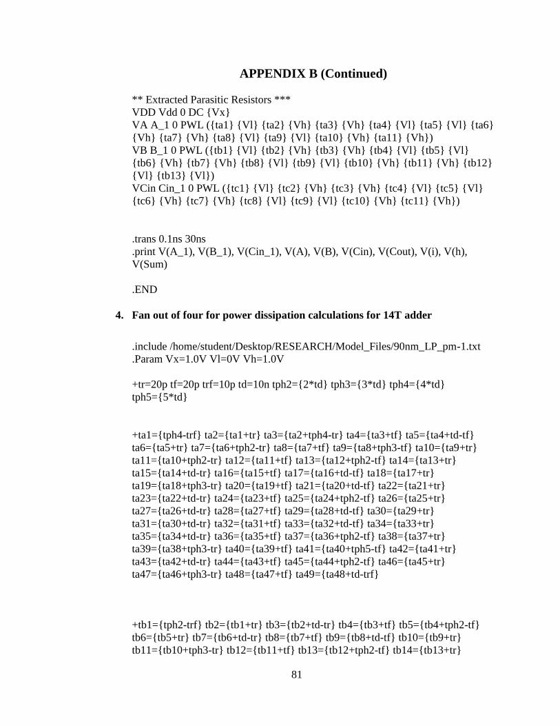
81
APPENDIX B (Continued)
** Extracted Parasitic Resistors ***
VDD Vdd 0 DC Vx
VA A_1 0 PWL (ta1 Vl ta2 Vh ta3 Vh ta4 Vl ta5 Vl ta6
Vh ta7 Vh ta8 Vl ta9 Vl ta10 Vh ta11 Vh)
VB B_1 0 PWL (tb1 Vl tb2 Vh tb3 Vh tb4 Vl tb5 Vl
tb6 Vh tb7 Vh tb8 Vl tb9 Vl tb10 Vh tb11 Vh tb12
Vl tb13 Vl)
VCin Cin_1 0 PWL (tc1 Vl tc2 Vh tc3 Vh tc4 Vl tc5 Vl
tc6 Vh tc7 Vh tc8 Vl tc9 Vl tc10 Vh tc11 Vh)
.trans 0.1ns 30ns
.print V(A_1), V(B_1), V(Cin_1), V(A), V(B), V(Cin), V(Cout), V(i), V(h),
V(Sum)
.END
4. Fan out of four for power dissipation calculations for 14T adder
.include /home/student/Desktop/RESEARCH/Model_Files/90nm_LP_pm-1.txt
.Param Vx=1.0V Vl=0V Vh=1.0V
+tr=20p tf=20p trf=10p td=10n tph2=2*td tph3=3*td tph4=4*td
tph5=5*td
+ta1=tph4-trf ta2=ta1+tr ta3=ta2+tph4-tr ta4=ta3+tf ta5=ta4+td-tf
ta6=ta5+tr ta7=ta6+tph2-tr ta8=ta7+tf ta9=ta8+tph3-tf ta10=ta9+tr
ta11=ta10+tph2-tr ta12=ta11+tf ta13=ta12+tph2-tf ta14=ta13+tr
ta15=ta14+td-tr ta16=ta15+tf ta17=ta16+td-tf ta18=ta17+tr
ta19=ta18+tph3-tr ta20=ta19+tf ta21=ta20+td-tf ta22=ta21+tr
ta23=ta22+td-tr ta24=ta23+tf ta25=ta24+tph2-tf ta26=ta25+tr
ta27=ta26+td-tr ta28=ta27+tf ta29=ta28+td-tf ta30=ta29+tr
ta31=ta30+td-tr ta32=ta31+tf ta33=ta32+td-tf ta34=ta33+tr
ta35=ta34+td-tr ta36=ta35+tf ta37=ta36+tph2-tf ta38=ta37+tr
ta39=ta38+tph3-tr ta40=ta39+tf ta41=ta40+tph5-tf ta42=ta41+tr
ta43=ta42+td-tr ta44=ta43+tf ta45=ta44+tph2-tf ta46=ta45+tr
ta47=ta46+tph3-tr ta48=ta47+tf ta49=ta48+td-trf
+tb1=tph2-trf tb2=tb1+tr tb3=tb2+td-tr tb4=tb3+tf tb5=tb4+tph2-tf
tb6=tb5+tr tb7=tb6+td-tr tb8=tb7+tf tb9=tb8+td-tf tb10=tb9+tr
tb11=tb10+tph3-tr tb12=tb11+tf tb13=tb12+tph2-tf tb14=tb13+tr

82
APPENDIX B (Continued)
tb15=tb14+tph2-tr tb16=tb15+tf tb17=tb16+tph2-tf tb18=tb17+tr
tb19=tb18+td-tr tb20=tb19+tf tb21=tb20+tph3-tf tb22=tb21+tr
tb23=tb22+td-tr tb24=tb23+tf tb25=tb24+td-tf tb26=tb25+tr
tb27=tb26+tph3-tr tb28=tb27+tf tb29=tb28+td-tf tb30=tb29+tr
tb31=tb30+td-tr tb32=tb31+tf tb33=tb32+tph3-tf tb34=tb33+tr
tb35=tb34+tph4-tr tb36=tb35+tf tb37=tb36+td-tf tb38=tb37+tr
tb39=tb38+tph2-tr tb40=tb39+tf tb41=tb40+tph3-tf tb42=tb41+tr
tb43=tb42+td-tr tb44=tb43+tf tb45=tb44+tph3-tf tb46=tb45+tr
tb47=tb46+tph2-tr tb48=tb47+tf tb49=tb48+td-tf tb50=tb49+tr
tb51=tb50+tph2-trf
+tc1=td-trf tc2=tc1+tr tc3=tc2+tph4-tr tc4=tc3+tf tc5=tc4+tph5-tf
tc6=tc5+tr tc7=tc6+tph2-tr tc8=tc7+tf tc9=tc8+td-tf tc10=tc9+tr
tc11=tc10+tph2-tr tc12=tc11+tf tc13=tc12+td-tf tc14=tc13+tr
tc15=tc14+tph3-tr tc16=tc15+tf tc17=tc16+tph3-tf tc18=tc17+tr
tc19=tc18+td-tr tc20=tc19+tf tc21=tc20+tph3-tf tc22=tc21+tr
tc23=tc22+td-tr tc24=tc23+tf tc25=tc24+td-tf tc26=tc25+tr
tc27=tc26+tph2-tr tc28=tc27+tf tc29=tc28+tph2-tf tc30=tc29+tr
tc31=tc30+tph2-tr tc32=tc31+tf tc33=tc32+tph3-tf tc34=tc33+tr
tc35=tc34+tph2-tr tc36=tc35+tf tc37=tc36+td-tf tc38=tc37+tr
tc39=tc38+tph3-tr tc40=tc39+tf tc41=tc40+tph4-tf tc42=tc41+tr
tc43=tc42+td-tr tc44=tc43+tf tc45=tc44+td-trf
Mn1 A B h gnd N L=0.09U W=0.18U AS=0.051P AD=0.108P PS=0.788U
PD=1.395U
Mn2 h A B gnd N L=0.09U W=0.18U AS=0.134P AD=0.051P PS=1.62U
PD=0.788U
Mn3 i h Gnd gnd N L=0.09U W=0.18U AS=0.08P AD=0.065P PS=1.158U
PD=0.878U
Mn4 Sum h Cin gnd N L=0.09U W=0.18U AS=0.117P AD=0.055P PS=1.47U
PD=0.675U
Mn5 h Cin Sum gnd N L=0.09U W=0.18U AS=0.055P AD=0.051P PS=0.675U
PD=0.788U
Mn6 Cout i Cin gnd N L=0.09U W=0.18U AS=0.117P AD=0.051P PS=1.47U
PD=0.652U
Mn7 A h Cout gnd N L=0.09U W=0.18U AS=0.051P AD=0.108P PS=0.652U
PD=1.395U
Mnmos@0 Cin Inv_Cin_1 Gnd gnd N L=0.09U W=0.54U AS=0.08P AD=0.117P
PS=1.158U
+PD=1.47U
Mnmos@1 Inv_Cin_1 Cin_1 Gnd gnd N L=0.09U W=0.18U AS=0.08P
AD=0.061P

83
APPENDIX B (Continued)
+PS=1.158U PD=0.99U
Mnmos@2 Gnd Inv_B_1 B gnd N L=0.09U W=0.54U AS=0.134P AD=0.08P
PS=1.62U
+PD=1.158U
Mnmos@3 Gnd B_1 Inv_B_1 gnd N L=0.09U W=0.18U AS=0.061P AD=0.08P
PS=0.99U
+PD=1.158U
Mnmos@4 Gnd Inv_A_1 A gnd N L=0.09U W=0.54U AS=0.108P AD=0.08P
PS=1.395U
+PD=1.158U
Mnmos@5 Gnd A_1 Inv_A_1 gnd N L=0.09U W=0.18U AS=0.061P AD=0.08P
PS=0.99U
+PD=1.158U
Mnmos@6 Cout_Buf_2 Inv_Buf_2 Gnd gnd N L=0.09U W=0.54U AS=0.08P
AD=0.182P
+PS=1.158U PD=2.07U
Mnmos@7 Inv_Buf_2 Cout Gnd gnd N L=0.09U W=0.18U AS=0.08P
AD=0.061P PS=1.158U
+PD=0.99U
Mnmos@8 Cout_Buf_4 Inv_Buf_4 Gnd gnd N L=0.09U W=0.54U AS=0.08P
AD=0.182P
+PS=1.158U PD=2.07U
Mnmos@9 Inv_Buf_4 Cout Gnd gnd N L=0.09U W=0.18U AS=0.08P
AD=0.061P PS=1.158U
+PD=0.99U
Mnmos@10 Cout_Buf_3 Inv_Buf_3 Gnd gnd N L=0.09U W=0.54U AS=0.08P
AD=0.182P
+PS=1.158U PD=2.07U
Mnmos@11 Inv_Buf_3 Cout Gnd gnd N L=0.09U W=0.18U AS=0.08P
AD=0.061P
+PS=1.158U PD=0.99U
Mnmos@12 Cout_Buf_1 Inv_Buf_1 Gnd gnd N L=0.09U W=0.54U AS=0.08P
AD=0.182P
+PS=1.158U PD=2.07U
Mnmos@13 Inv_Buf_1 Cout Gnd gnd N L=0.09U W=0.18U AS=0.08P
AD=0.061P
+PS=1.158U PD=0.99U
Mnmos@14 Sum_INV_3 Sum Gnd gnd N L=0.09U W=0.18U AS=0.08P
AD=0.061P PS=1.158U
+PD=0.99U
Mnmos@15 Sum_Buf_3 Sum_INV_3 Gnd gnd N L=0.09U W=0.54U AS=0.08P
AD=0.182P
+PS=1.158U PD=2.07U
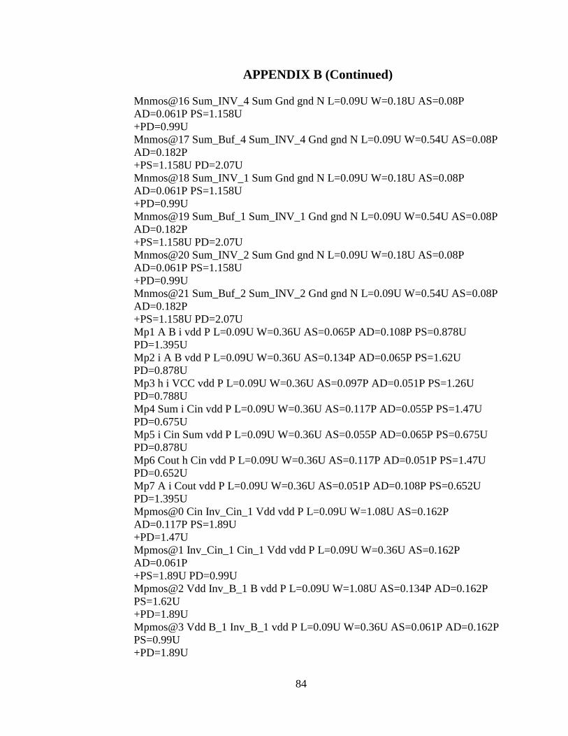
84
APPENDIX B (Continued)
Mnmos@16 Sum_INV_4 Sum Gnd gnd N L=0.09U W=0.18U AS=0.08P
AD=0.061P PS=1.158U
+PD=0.99U
Mnmos@17 Sum_Buf_4 Sum_INV_4 Gnd gnd N L=0.09U W=0.54U AS=0.08P
AD=0.182P
+PS=1.158U PD=2.07U
Mnmos@18 Sum_INV_1 Sum Gnd gnd N L=0.09U W=0.18U AS=0.08P
AD=0.061P PS=1.158U
+PD=0.99U
Mnmos@19 Sum_Buf_1 Sum_INV_1 Gnd gnd N L=0.09U W=0.54U AS=0.08P
AD=0.182P
+PS=1.158U PD=2.07U
Mnmos@20 Sum_INV_2 Sum Gnd gnd N L=0.09U W=0.18U AS=0.08P
AD=0.061P PS=1.158U
+PD=0.99U
Mnmos@21 Sum_Buf_2 Sum_INV_2 Gnd gnd N L=0.09U W=0.54U AS=0.08P
AD=0.182P
+PS=1.158U PD=2.07U
Mp1 A B i vdd P L=0.09U W=0.36U AS=0.065P AD=0.108P PS=0.878U
PD=1.395U
Mp2 i A B vdd P L=0.09U W=0.36U AS=0.134P AD=0.065P PS=1.62U
PD=0.878U
Mp3 h i VCC vdd P L=0.09U W=0.36U AS=0.097P AD=0.051P PS=1.26U
PD=0.788U
Mp4 Sum i Cin vdd P L=0.09U W=0.36U AS=0.117P AD=0.055P PS=1.47U
PD=0.675U
Mp5 i Cin Sum vdd P L=0.09U W=0.36U AS=0.055P AD=0.065P PS=0.675U
PD=0.878U
Mp6 Cout h Cin vdd P L=0.09U W=0.36U AS=0.117P AD=0.051P PS=1.47U
PD=0.652U
Mp7 A i Cout vdd P L=0.09U W=0.36U AS=0.051P AD=0.108P PS=0.652U
PD=1.395U
Mpmos@0 Cin Inv_Cin_1 Vdd vdd P L=0.09U W=1.08U AS=0.162P
AD=0.117P PS=1.89U
+PD=1.47U
Mpmos@1 Inv_Cin_1 Cin_1 Vdd vdd P L=0.09U W=0.36U AS=0.162P
AD=0.061P
+PS=1.89U PD=0.99U
Mpmos@2 Vdd Inv_B_1 B vdd P L=0.09U W=1.08U AS=0.134P AD=0.162P
PS=1.62U
+PD=1.89U
Mpmos@3 Vdd B_1 Inv_B_1 vdd P L=0.09U W=0.36U AS=0.061P AD=0.162P
PS=0.99U
+PD=1.89U

85
APPENDIX B (Continued)
Mpmos@4 Vdd Inv_A_1 A vdd P L=0.09U W=1.08U AS=0.108P AD=0.162P
PS=1.395U
+PD=1.89U
Mpmos@5 Vdd A_1 Inv_A_1 vdd P L=0.09U W=0.36U AS=0.061P AD=0.162P
PS=0.99U
+PD=1.89U
Mpmos@6 Cout_Buf_2 Inv_Buf_2 Vdd vdd P L=0.09U W=1.08U AS=0.162P
AD=0.182P
+PS=1.89U PD=2.07U
Mpmos@7 Inv_Buf_2 Cout Vdd vdd P L=0.09U W=0.36U AS=0.162P
AD=0.061P PS=1.89U
+PD=0.99U
Mpmos@8 Cout_Buf_4 Inv_Buf_4 Vdd vdd P L=0.09U W=1.08U AS=0.162P
AD=0.182P
+PS=1.89U PD=2.07U
Mpmos@9 Inv_Buf_4 Cout Vdd vdd P L=0.09U W=0.36U AS=0.162P
AD=0.061P PS=1.89U
+PD=0.99U
Mpmos@10 Cout_Buf_3 Inv_Buf_3 Vdd vdd P L=0.09U W=1.08U AS=0.162P
AD=0.182P
+PS=1.89U PD=2.07U
Mpmos@11 Inv_Buf_3 Cout Vdd vdd P L=0.09U W=0.36U AS=0.162P
AD=0.061P
+PS=1.89U PD=0.99U
Mpmos@12 Cout_Buf_1 Inv_Buf_1 Vdd vdd P L=0.09U W=1.08U AS=0.162P
AD=0.182P
+PS=1.89U PD=2.07U
Mpmos@13 Inv_Buf_1 Cout Vdd vdd P L=0.09U W=0.36U AS=0.162P
AD=0.061P
+PS=1.89U PD=0.99U
Mpmos@14 Sum_INV_3 Sum Vdd vdd P L=0.09U W=0.36U AS=0.162P
AD=0.061P PS=1.89U
+PD=0.99U
Mpmos@15 Sum_Buf_3 Sum_INV_3 Vdd vdd P L=0.09U W=1.08U AS=0.162P
AD=0.182P
+PS=1.89U PD=2.07U
Mpmos@16 Sum_INV_4 Sum Vdd vdd P L=0.09U W=0.36U AS=0.162P
AD=0.061P PS=1.89U
+PD=0.99U
Mpmos@17 Sum_Buf_4 Sum_INV_4 Vdd vdd P L=0.09U W=1.08U AS=0.162P
AD=0.182P
+PS=1.89U PD=2.07U
Mpmos@18 Sum_INV_1 Sum Vdd vdd P L=0.09U W=0.36U AS=0.162P
AD=0.061P PS=1.89U
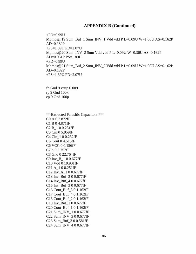
86
APPENDIX B (Continued)
+PD=0.99U
Mpmos@19 Sum_Buf_1 Sum_INV_1 Vdd vdd P L=0.09U W=1.08U AS=0.162P
AD=0.182P
+PS=1.89U PD=2.07U
Mpmos@20 Sum_INV_2 Sum Vdd vdd P L=0.09U W=0.36U AS=0.162P
AD=0.061P PS=1.89U
+PD=0.99U
Mpmos@21 Sum_Buf_2 Sum_INV_2 Vdd vdd P L=0.09U W=1.08U AS=0.162P
AD=0.182P
+PS=1.89U PD=2.07U
fp Gnd 9 vtstp 0.009
rp 9 Gnd 100k
cp 9 Gnd 100p
** Extracted Parasitic Capacitors ***
C0 A 0 7.872fF
C1 B 0 4.871fF
C2 B_1 0 0.251fF
C3 Cin 0 5.959fF
C4 Cin_1 0 0.232fF
C5 Cout 0 4.513fF
C6 VCC 0 0.156fF
C7 h 0 5.757fF
C8 Gnd 0 22.764fF
C9 Inv_B_1 0 0.677fF
C10 Vdd 0 19.901fF
C11 A_1 0 0.251fF
C12 Inv_A_1 0 0.677fF
C13 Inv_Buf_2 0 0.677fF
C14 Inv_Buf_4 0 0.677fF
C15 Inv_Buf_3 0 0.677fF
C16 Cout_Buf_3 0 1.162fF
C17 Cout_Buf_4 0 1.162fF
C18 Cout_Buf_2 0 1.162fF
C19 Inv_Buf_1 0 0.677fF
C20 Cout_Buf_1 0 1.162fF
C21 Sum_INV_1 0 0.677fF
C22 Sum_INV_3 0 0.677fF
C23 Sum_Buf_3 0 0.581fF
C24 Sum_INV_4 0 0.677fF

87
APPENDIX B (Continued)
C25 Sum_Buf_4 0 0.581fF
C26 Sum_INV_2 0 0.677fF
C27 Sum 0 1.573fF
C28 Sum_Buf_1 0 0.581fF
C29 Sum_Buf_2 0 0.581fF
C30 i 0 3.065fF
C31 Inv_Cin_1 0 0.677fF
** Extracted Parasitic Resistors ***
vdd Vdd Gnd DC Vx
vtstp Vdd Vcc 0
VA A_1 0 PWL (ta1 Vl ta2 Vh ta3 Vh ta4 Vl ta5 Vl ta6
Vh ta7 Vh ta8 Vl ta9 Vl ta10 Vh
+ta11 Vh ta12 Vl ta13 Vl ta14 Vh ta15 Vh ta16 Vl
ta17 Vl ta18 Vh ta19 Vh
+ta20 Vl ta21 Vl ta22 Vh ta23 Vh ta24 Vl ta25 Vl
ta26 Vh ta27 Vh ta28 Vl ta29 Vl +ta30 Vh ta31 Vh
ta32 Vl ta33 Vl ta34 Vh ta35 Vh ta36 Vl ta37 Vl
ta38 Vh ta39 Vh +ta40 Vl ta41 Vl ta42 Vh ta43 Vh
ta44 Vl ta45 Vl ta46 Vh ta47 Vh ta48 Vl ta49 Vl)
VB B_1 0 PWL (tb1 Vl tb2 Vh tb3 Vh tb4 Vl tb5 Vl
tb6 Vh tb7 Vh tb8 Vl tb9 Vl tb10 Vh tb11 Vh
+tb12 Vl tb13 Vl tb14 Vh tb15 Vh tb16 Vl tb17 Vl
tb18 Vh tb19 Vh tb20 Vl tb21 Vl tb22 Vh tb23 Vh
tb24 Vl tb25 Vl
+tb26 Vh tb27 Vh tb28 Vl tb29 Vl tb30 Vh tb31 Vh
tb32 Vl tb33 Vl tb34 Vh tb35 Vh
+tb36 Vl tb37 Vl tb38 Vh tb39 Vh tb40 Vl tb41 Vl
tb42 Vh tb43 Vh tb44 Vl tb45 Vl tb46 Vh tb47 Vh
tb48 Vl tb49 Vl tb50 Vh tb51 Vh)
VCin Cin_1 0 PWL (tc1 Vl tc2 Vh tc3 Vh tc4 Vl tc5 Vl
tc6 Vh tc7 Vh tc8 Vl tc9 Vl tc10 Vh tc11 Vh tc12
Vl tc13 Vl tc14 Vh tc15 Vh tc16 Vl tc17 Vl tc18
Vh tc19 Vh tc20 Vl tc21 Vl tc22 Vh tc23 Vh tc24
Vl tc25 Vl tc26 Vh tc27 Vh tc28 Vl tc29 Vl tc30
Vh tc31 Vh tc32 Vl tc33 Vl tc34 Vh tc35 Vh tc36
Vl tc37 Vl tc38 Vh tc39 Vh tc40 Vl tc41 Vl tc42
Vh tc43 Vh tc44 Vl tc45 Vl)
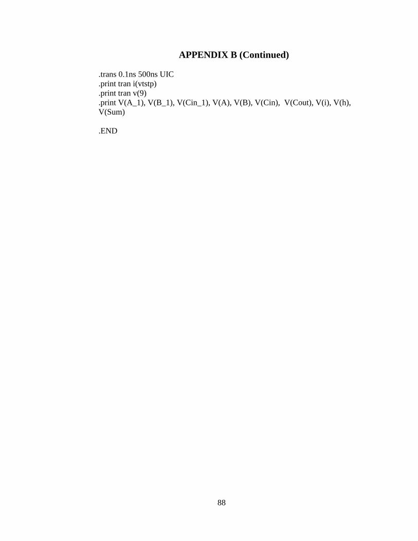
88
APPENDIX B (Continued)
.trans 0.1ns 500ns UIC
.print tran i(vtstp)
.print tran v(9)
.print V(A_1), V(B_1), V(Cin_1), V(A), V(B), V(Cin), V(Cout), V(i), V(h),
V(Sum)
.END
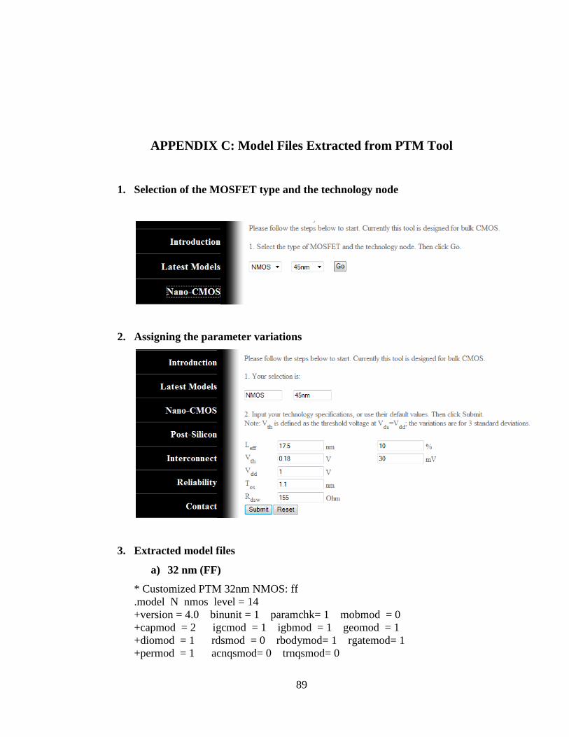
89
APPENDIX C: Model Files Extracted from PTM Tool
1. Selection of the MOSFET type and the technology node
2. Assigning the parameter variations
3. Extracted model files
a) 32 nm (FF)
* Customized PTM 32nm NMOS: ff
.model N nmos level = 14
+version = 4.0 binunit = 1 paramchk= 1 mobmod = 0
+capmod = 2 igcmod = 1 igbmod = 1 geomod = 1
+diomod = 1 rdsmod = 0 rbodymod= 1 rgatemod= 1
+permod = 1 acnqsmod= 0 trnqsmod= 0

90
APPENDIX C (Continued)
* parameters related to the technology node
+tnom = 27 epsrox = 3.9
+eta0 = 0.0042 nfactor = 2.3 wint = 5e-09
+cgso = 8.5e-11 cgdo = 8.5e-11 xl = -1.4e-08
* parameters customized by the user
+toxe = 1.95e-09 toxp = 1.3e-09 toxm = 1.95e-09 toxref = 1.95e-09
+dtox = 6.5e-10 lint = 0
+vth0 = 0.377 k1 = 0.455 u0 = 0.05445 vsat = 178470
+rdsw = 190 ndep = 2.69e+18 xj = 1.44e-08
* secondary parameters
+ll = 0 wl = 0 lln = 1 wln = 1
+lw = 0 ww = 0 lwn = 1 wwn = 1
+lwl = 0 wwl = 0 xpart = 0
+k2 = 0.01 k3 = 0
+k3b = 0 w0 = 2.5e-006 dvt0 = 1 dvt1 = 2
+dvt2 = -0.032 dvt0w = 0 dvt1w = 0 dvt2w = 0
+dsub = 0.1 minv = 0.05 voffl = 0 dvtp0 = 1.0e-009
+dvtp1 = 0.1 lpe0 = 0 lpeb = 0
+ngate = 2e+020 nsd = 2e+020 phin = 0
+cdsc = 0.000 cdscb = 0 cdscd = 0 cit = 0
+voff = -0.13 etab = 0
+vfb = -0.55 ua = 6e-010 ub = 1.2e-018
+uc = 0 a0 = 1.0 ags = 1e-020
+a1 = 0 a2 = 1.0 b0 = 0 b1 = 0
+keta = 0.04 dwg = 0 dwb = 0 pclm = 0.04
+pdiblc1 = 0.001 pdiblc2 = 0.001 pdiblcb = -0.005 drout = 0.5
+pvag = 1e-020 delta = 0.01 pscbe1 = 8.14e+008 pscbe2 = 1e-007
+fprout = 0.2 pdits = 0.08 pditsd = 0.23 pditsl = 2.3e+006
+rsh = 5 rsw = 85 rdw = 85
+rdswmin = 0 rdwmin = 0 rswmin = 0 prwg = 0
+prwb = 6.8e-011 wr = 1 alpha0 = 0.074 alpha1 = 0.005
+beta0 = 30 agidl = 0.0002 bgidl = 2.1e+009 cgidl = 0.0002
+egidl = 0.8
+aigbacc = 0.012 bigbacc = 0.0028 cigbacc = 0.002
+nigbacc = 1 aigbinv = 0.014 bigbinv = 0.004 cigbinv = 0.004
+eigbinv = 1.1 nigbinv = 3 aigc = 0.012 bigc = 0.0028
+cigc = 0.002 aigsd = 0.012 bigsd = 0.0028 cigsd = 0.002
+nigc = 1 poxedge = 1 pigcd = 1 ntox = 1
+xrcrg1 = 12 xrcrg2 = 5
+cgbo = 2.56e-011 cgdl = 2.653e-10

91
APPENDIX C (Continued)
+cgsl = 2.653e-10 ckappas = 0.03 ckappad = 0.03 acde = 1
+moin = 15 noff = 0.9 voffcv = 0.02
+kt1 = -0.11 kt1l = 0 kt2 = 0.022 ute = -1.5
+ua1 = 4.31e-009 ub1 = 7.61e-018 uc1 = -5.6e-011 prt = 0
+at = 33000
+fnoimod = 1 tnoimod = 0
+jss = 0.0001 jsws = 1e-011 jswgs = 1e-010 njs = 1
+ijthsfwd= 0.01 ijthsrev= 0.001 bvs = 10 xjbvs = 1
+jsd = 0.0001 jswd = 1e-011 jswgd = 1e-010 njd = 1
+ijthdfwd= 0.01 ijthdrev= 0.001 bvd = 10 xjbvd = 1
+pbs = 1 cjs = 0.0005 mjs = 0.5 pbsws = 1
+cjsws = 5e-010 mjsws = 0.33 pbswgs = 1 cjswgs = 3e-010
+mjswgs = 0.33 pbd = 1 cjd = 0.0005 mjd = 0.5
+pbswd = 1 cjswd = 5e-010 mjswd = 0.33 pbswgd = 1
+cjswgd = 5e-010 mjswgd = 0.33 tpb = 0.005 tcj = 0.001
+tpbsw = 0.005 tcjsw = 0.001 tpbswg = 0.005 tcjswg = 0.001
+xtis = 3 xtid = 3
+dmcg = 0e-006 dmci = 0e-006 dmdg = 0e-006 dmcgt = 0e-007
+dwj = 0.0e-008 xgw = 0e-007 xgl = 0e-008
+rshg = 0.4 gbmin = 1e-010 rbpb = 5 rbpd = 15
+rbps = 15 rbdb = 15 rbsb = 15 ngcon = 1
* Customized PTM 32nm PMOS: ff
.model P pmos level = 14
+version = 4.0 binunit = 1 paramchk= 1 mobmod = 0
+capmod = 2 igcmod = 1 igbmod = 1 geomod = 1
+diomod = 1 rdsmod = 0 rbodymod= 1 rgatemod= 1
+permod = 1 acnqsmod= 0 trnqsmod= 0
* parameters related to the technology node
+tnom = 27 epsrox = 3.9
+eta0 = 0.0042 nfactor = 2.3 wint = 5e-09
+cgso = 8.5e-11 cgdo = 8.5e-11 xl = -1.4e-08
* parameters customized by the user
+toxe = 2.05e-09 toxp = 1.3e-09 toxm = 2.05e-09 toxref = 2.05e-09

92
APPENDIX C (Continued)
+dtox = 7.5e-10 lint = 0
+vth0 = -0.332 k1 = 0.42 u0 = 0.00682 vsat = 70000
+rdsw = 240 ndep = 2.12e+18 xj = 1.44e-08
*secondary parameters
+ll = 0 wl = 0 lln = 1 wln = 1
+lw = 0 ww = 0 lwn = 1 wwn = 1
+lwl = 0 wwl = 0 xpart = 0
+k2 = -0.01 k3 = 0
+k3b = 0 w0 = 2.5e-006 dvt0 = 1 dvt1 = 2
+dvt2 = -0.032 dvt0w = 0 dvt1w = 0 dvt2w = 0
+dsub = 0.1 minv = 0.05 voffl = 0 dvtp0 = 1e-009
+dvtp1 = 0.05 lpe0 = 0 lpeb = 0
+ngate = 2e+020 nsd = 2e+020 phin = 0
+cdsc = 0.000 cdscb = 0 cdscd = 0 cit = 0
+voff = -0.126 etab = 0
+vfb = 0.55 ua = 2.0e-009 ub = 0.5e-018
+uc = 0 a0 = 1.0 ags = 1e-020
+a1 = 0 a2 = 1 b0 = -1e-020 b1 = 0
+keta = -0.047 dwg = 0 dwb = 0 pclm = 0.12
+pdiblc1 = 0.001 pdiblc2 = 0.001 pdiblcb = 3.4e-008 drout = 0.56
+pvag = 1e-020 delta = 0.01 pscbe1 = 8.14e+008 pscbe2 = 9.58e-
007
+fprout = 0.2 pdits = 0.08 pditsd = 0.23 pditsl = 2.3e+006
+rsh = 5 rsw = 85 rdw = 85
+rdswmin = 0 rdwmin = 0 rswmin = 0 prwg = 3.22e-008
+prwb = 6.8e-011 wr = 1 alpha0 = 0.074 alpha1 = 0.005
+beta0 = 30 agidl = 0.0002 bgidl = 2.1e+009 cgidl = 0.0002
+egidl = 0.8
+aigbacc = 0.012 bigbacc = 0.0028 cigbacc = 0.002
+nigbacc = 1 aigbinv = 0.014 bigbinv = 0.004 cigbinv = 0.004
+eigbinv = 1.1 nigbinv = 3 aigc = 0.69 bigc = 0.0012
+cigc = 0.0008 aigsd = 0.0087 bigsd = 0.0012 cigsd = 0.0008
+nigc = 1 poxedge = 1 pigcd = 1 ntox = 1
+xrcrg1 = 12 xrcrg2 = 5
+cgbo = 2.56e-011 cgdl = 2.653e-10
+cgsl = 2.653e-10 ckappas = 0.03 ckappad = 0.03 acde = 1
+moin = 15 noff = 0.9 voffcv = 0.02
+kt1 = -0.11 kt1l = 0 kt2 = 0.022 ute = -1.5
+ua1 = 4.31e-009 ub1 = 7.61e-018 uc1 = -5.6e-011 prt = 0
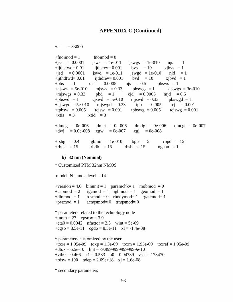
93
APPENDIX C (Continued)
+at = 33000
+fnoimod = 1 tnoimod = 0
+jss = 0.0001 jsws = 1e-011 jswgs = 1e-010 njs = 1
+ijthsfwd= 0.01 ijthsrev= 0.001 bvs = 10 xjbvs = 1
+jsd = 0.0001 jswd = 1e-011 jswgd = 1e-010 njd = 1
+ijthdfwd= 0.01 ijthdrev= 0.001 bvd = 10 xjbvd = 1
+pbs = 1 cjs = 0.0005 mjs = 0.5 pbsws = 1
+cjsws = 5e-010 mjsws = 0.33 pbswgs = 1 cjswgs = 3e-010
+mjswgs = 0.33 pbd = 1 cjd = 0.0005 mjd = 0.5
+pbswd = 1 cjswd = 5e-010 mjswd = 0.33 pbswgd = 1
+cjswgd = 5e-010 mjswgd = 0.33 tpb = 0.005 tcj = 0.001
+tpbsw = 0.005 tcjsw = 0.001 tpbswg = 0.005 tcjswg = 0.001
+xtis = 3 xtid = 3
+dmcg = 0e-006 dmci = 0e-006 dmdg = 0e-006 dmcgt = 0e-007
+dwj = 0.0e-008 xgw = 0e-007 xgl = 0e-008
+rshg = 0.4 gbmin = 1e-010 rbpb = 5 rbpd = 15
+rbps = 15 rbdb = 15 rbsb = 15 ngcon = 1
b) 32 nm (Nominal)
* Customized PTM 32nm NMOS
.model N nmos level = 14
+version = 4.0 binunit = 1 paramchk= 1 mobmod = 0
+capmod = 2 igcmod = 1 igbmod = 1 geomod = 1
+diomod = 1 rdsmod = 0 rbodymod= 1 rgatemod= 1
+permod = 1 acnqsmod= 0 trnqsmod= 0
* parameters related to the technology node
+tnom = 27 epsrox = 3.9
+eta0 = 0.0042 nfactor = 2.3 wint = 5e-09
+cgso = 8.5e-11 cgdo = 8.5e-11 xl = -1.4e-08
* parameters customized by the user
+toxe = 1.95e-09 toxp = 1.3e-09 toxm = 1.95e-09 toxref = 1.95e-09
+dtox = 6.5e-10 lint = -9.99999999999999e-10
+vth0 = 0.466 k1 = 0.533 u0 = 0.04789 vsat = 178470
+rdsw = 190 ndep = 2.69e+18 xj = 1.6e-08
* secondary parameters

94
APPENDIX C (Continued)
+ll = 0 wl = 0 lln = 1 wln = 1
+lw = 0 ww = 0 lwn = 1 wwn = 1
+lwl = 0 wwl = 0 xpart = 0
+k2 = 0.01 k3 = 0
+k3b = 0 w0 = 2.5e-006 dvt0 = 1 dvt1 = 2
+dvt2 = -0.032 dvt0w = 0 dvt1w = 0 dvt2w = 0
+dsub = 0.1 minv = 0.05 voffl = 0 dvtp0 = 1.0e-009
+dvtp1 = 0.1 lpe0 = 0 lpeb = 0
+ngate = 2e+020 nsd = 2e+020 phin = 0
+cdsc = 0.000 cdscb = 0 cdscd = 0 cit = 0
+voff = -0.13 etab = 0
+vfb = -0.55 ua = 6e-010 ub = 1.2e-018
+uc = 0 a0 = 1.0 ags = 1e-020
+a1 = 0 a2 = 1.0 b0 = 0 b1 = 0
+keta = 0.04 dwg = 0 dwb = 0 pclm = 0.04
+pdiblc1 = 0.001 pdiblc2 = 0.001 pdiblcb = -0.005 drout = 0.5
+pvag = 1e-020 delta = 0.01 pscbe1 = 8.14e+008 pscbe2 = 1e-007
+fprout = 0.2 pdits = 0.08 pditsd = 0.23 pditsl = 2.3e+006
+rsh = 5 rsw = 85 rdw = 85
+rdswmin = 0 rdwmin = 0 rswmin = 0 prwg = 0
+prwb = 6.8e-011 wr = 1 alpha0 = 0.074 alpha1 = 0.005
+beta0 = 30 agidl = 0.0002 bgidl = 2.1e+009 cgidl = 0.0002
+egidl = 0.8
+aigbacc = 0.012 bigbacc = 0.0028 cigbacc = 0.002
+nigbacc = 1 aigbinv = 0.014 bigbinv = 0.004 cigbinv = 0.004
+eigbinv = 1.1 nigbinv = 3 aigc = 0.012 bigc = 0.0028
+cigc = 0.002 aigsd = 0.012 bigsd = 0.0028 cigsd = 0.002
+nigc = 1 poxedge = 1 pigcd = 1 ntox = 1
+xrcrg1 = 12 xrcrg2 = 5
+cgbo = 2.56e-011 cgdl = 2.653e-10
+cgsl = 2.653e-10 ckappas = 0.03 ckappad = 0.03 acde = 1
+moin = 15 noff = 0.9 voffcv = 0.02
+kt1 = -0.11 kt1l = 0 kt2 = 0.022 ute = -1.5
+ua1 = 4.31e-009 ub1 = 7.61e-018 uc1 = -5.6e-011 prt = 0
+at = 33000
+fnoimod = 1 tnoimod = 0
+jss = 0.0001 jsws = 1e-011 jswgs = 1e-010 njs = 1
+ijthsfwd= 0.01 ijthsrev= 0.001 bvs = 10 xjbvs = 1

95
APPENDIX C (Continued)
+jsd = 0.0001 jswd = 1e-011 jswgd = 1e-010 njd = 1
+ijthdfwd= 0.01 ijthdrev= 0.001 bvd = 10 xjbvd = 1
+pbs = 1 cjs = 0.0005 mjs = 0.5 pbsws = 1
+cjsws = 5e-010 mjsws = 0.33 pbswgs = 1 cjswgs = 3e-010
+mjswgs = 0.33 pbd = 1 cjd = 0.0005 mjd = 0.5
+pbswd = 1 cjswd = 5e-010 mjswd = 0.33 pbswgd = 1
+cjswgd = 5e-010 mjswgd = 0.33 tpb = 0.005 tcj = 0.001
+tpbsw = 0.005 tcjsw = 0.001 tpbswg = 0.005 tcjswg = 0.001
+xtis = 3 xtid = 3
+dmcg = 0e-006 dmci = 0e-006 dmdg = 0e-006 dmcgt = 0e-007
+dwj = 0.0e-008 xgw = 0e-007 xgl = 0e-008
+rshg = 0.4 gbmin = 1e-010 rbpb = 5 rbpd = 15
+rbps = 15 rbdb = 15 rbsb = 15 ngcon = 1
* Customized PTM 32nm PMOS
.model P pmos level = 14
+version = 4.0 binunit = 1 paramchk= 1 mobmod = 0
+capmod = 2 igcmod = 1 igbmod = 1 geomod = 1
+diomod = 1 rdsmod = 0 rbodymod= 1 rgatemod= 1
+permod = 1 acnqsmod= 0 trnqsmod= 0
* parameters related to the technology node
+tnom = 27 epsrox = 3.9
+eta0 = 0.0042 nfactor = 2.3 wint = 5e-09
+cgso = 8.5e-11 cgdo = 8.5e-11 xl = -1.4e-08
* parameters customized by the user
+toxe = 2.05e-09 toxp = 1.3e-09 toxm = 2.05e-09 toxref = 2.05e-09
+dtox = 7.5e-10 lint = -9.99999999999999e-10
+vth0 = -0.422 k1 = 0.498 u0 = 0.00513 vsat = 70000
+rdsw = 240 ndep = 2.12e+18 xj = 1.6e-08
*secondary parameters
+ll = 0 wl = 0 lln = 1 wln = 1
+lw = 0 ww = 0 lwn = 1 wwn = 1
+lwl = 0 wwl = 0 xpart = 0
+k2 = -0.01 k3 = 0
+k3b = 0 w0 = 2.5e-006 dvt0 = 1 dvt1 = 2

96
APPENDIX C (Continued)
+dvt2 = -0.032 dvt0w = 0 dvt1w = 0 dvt2w = 0
+dsub = 0.1 minv = 0.05 voffl = 0 dvtp0 = 1e-009
+dvtp1 = 0.05 lpe0 = 0 lpeb = 0
+ngate = 2e+020 nsd = 2e+020 phin = 0
+cdsc = 0.000 cdscb = 0 cdscd = 0 cit = 0
+voff = -0.126 etab = 0
+vfb = 0.55 ua = 2.0e-009 ub = 0.5e-018
+uc = 0 a0 = 1.0 ags = 1e-020
+a1 = 0 a2 = 1 b0 = -1e-020 b1 = 0
+keta = -0.047 dwg = 0 dwb = 0 pclm = 0.12
+pdiblc1 = 0.001 pdiblc2 = 0.001 pdiblcb = 3.4e-008 drout = 0.56
+pvag = 1e-020 delta = 0.01 pscbe1 = 8.14e+008 pscbe2 = 9.58e-
007
+fprout = 0.2 pdits = 0.08 pditsd = 0.23 pditsl = 2.3e+006
+rsh = 5 rsw = 85 rdw = 85
+rdswmin = 0 rdwmin = 0 rswmin = 0 prwg = 3.22e-008
+prwb = 6.8e-011 wr = 1 alpha0 = 0.074 alpha1 = 0.005
+beta0 = 30 agidl = 0.0002 bgidl = 2.1e+009 cgidl = 0.0002
+egidl = 0.8
+aigbacc = 0.012 bigbacc = 0.0028 cigbacc = 0.002
+nigbacc = 1 aigbinv = 0.014 bigbinv = 0.004 cigbinv = 0.004
+eigbinv = 1.1 nigbinv = 3 aigc = 0.69 bigc = 0.0012
+cigc = 0.0008 aigsd = 0.0087 bigsd = 0.0012 cigsd = 0.0008
+nigc = 1 poxedge = 1 pigcd = 1 ntox = 1
+xrcrg1 = 12 xrcrg2 = 5
+cgbo = 2.56e-011 cgdl = 2.653e-10
+cgsl = 2.653e-10 ckappas = 0.03 ckappad = 0.03 acde = 1
+moin = 15 noff = 0.9 voffcv = 0.02
+kt1 = -0.11 kt1l = 0 kt2 = 0.022 ute = -1.5
+ua1 = 4.31e-009 ub1 = 7.61e-018 uc1 = -5.6e-011 prt = 0
+at = 33000
+fnoimod = 1 tnoimod = 0
+jss = 0.0001 jsws = 1e-011 jswgs = 1e-010 njs = 1
+ijthsfwd= 0.01 ijthsrev= 0.001 bvs = 10 xjbvs = 1
+jsd = 0.0001 jswd = 1e-011 jswgd = 1e-010 njd = 1
+ijthdfwd= 0.01 ijthdrev= 0.001 bvd = 10 xjbvd = 1
+pbs = 1 cjs = 0.0005 mjs = 0.5 pbsws = 1
+cjsws = 5e-010 mjsws = 0.33 pbswgs = 1 cjswgs = 3e-010

97
APPENDIX C (Continued)
+mjswgs = 0.33 pbd = 1 cjd = 0.0005 mjd = 0.5
+pbswd = 1 cjswd = 5e-010 mjswd = 0.33 pbswgd = 1
+cjswgd = 5e-010 mjswgd = 0.33 tpb = 0.005 tcj = 0.001
+tpbsw = 0.005 tcjsw = 0.001 tpbswg = 0.005 tcjswg = 0.001
+xtis = 3 xtid = 3
+dmcg = 0e-006 dmci = 0e-006 dmdg = 0e-006 dmcgt = 0e-007
+dwj = 0.0e-008 xgw = 0e-007 xgl = 0e-008
+rshg = 0.4 gbmin = 1e-010 rbpb = 5 rbpd = 15
+rbps = 15 rbdb = 15 rbsb = 15 ngcon = 1
c) 32 nm (SS)
* Customized PTM 32nm NMOS: ss
.model N nmos level = 14
+version = 4.0 binunit = 1 paramchk= 1 mobmod = 0
+capmod = 2 igcmod = 1 igbmod = 1 geomod = 1
+diomod = 1 rdsmod = 0 rbodymod= 1 rgatemod= 1
+permod = 1 acnqsmod= 0 trnqsmod= 0
* parameters related to the technology node
+tnom = 27 epsrox = 3.9
+eta0 = 0.0042 nfactor = 2.3 wint = 5e-09
+cgso = 8.5e-11 cgdo = 8.5e-11 xl = -1.4e-08
* parameters customized by the user
+toxe = 1.95e-09 toxp = 1.3e-09 toxm = 1.95e-09 toxref = 1.95e-09
+dtox = 6.5e-10 lint = -2e-09
+vth0 = 0.553 k1 = 0.609 u0 = 0.04228 vsat = 178470
+rdsw = 190 ndep = 3.51e+18 xj = 1.76e-08
* secondary parameters
+ll = 0 wl = 0 lln = 1 wln = 1
+lw = 0 ww = 0 lwn = 1 wwn = 1
+lwl = 0 wwl = 0 xpart = 0
+k2 = 0.01 k3 = 0
+k3b = 0 w0 = 2.5e-006 dvt0 = 1 dvt1 = 2
+dvt2 = -0.032 dvt0w = 0 dvt1w = 0 dvt2w = 0
+dsub = 0.1 minv = 0.05 voffl = 0 dvtp0 = 1.0e-009
+dvtp1 = 0.1 lpe0 = 0 lpeb = 0
+ngate = 2e+020 nsd = 2e+020 phin = 0

98
APPENDIX C (Continued)
+cdsc = 0.000 cdscb = 0 cdscd = 0 cit = 0
+voff = -0.13 etab = 0
+vfb = -0.55 ua = 6e-010 ub = 1.2e-018
+uc = 0 a0 = 1.0 ags = 1e-020
+a1 = 0 a2 = 1.0 b0 = 0 b1 = 0
+keta = 0.04 dwg = 0 dwb = 0 pclm = 0.04
+pdiblc1 = 0.001 pdiblc2 = 0.001 pdiblcb = -0.005 drout = 0.5
+pvag = 1e-020 delta = 0.01 pscbe1 = 8.14e+008 pscbe2 = 1e-007
+fprout = 0.2 pdits = 0.08 pditsd = 0.23 pditsl = 2.3e+006
+rsh = 5 rsw = 85 rdw = 85
+rdswmin = 0 rdwmin = 0 rswmin = 0 prwg = 0
+prwb = 6.8e-011 wr = 1 alpha0 = 0.074 alpha1 = 0.005
+beta0 = 30 agidl = 0.0002 bgidl = 2.1e+009 cgidl = 0.0002
+egidl = 0.8
+aigbacc = 0.012 bigbacc = 0.0028 cigbacc = 0.002
+nigbacc = 1 aigbinv = 0.014 bigbinv = 0.004 cigbinv = 0.004
+eigbinv = 1.1 nigbinv = 3 aigc = 0.012 bigc = 0.0028
+cigc = 0.002 aigsd = 0.012 bigsd = 0.0028 cigsd = 0.002
+nigc = 1 poxedge = 1 pigcd = 1 ntox = 1
+xrcrg1 = 12 xrcrg2 = 5
+cgbo = 2.56e-011 cgdl = 2.653e-10
+cgsl = 2.653e-10 ckappas = 0.03 ckappad = 0.03 acde = 1
+moin = 15 noff = 0.9 voffcv = 0.02
+kt1 = -0.11 kt1l = 0 kt2 = 0.022 ute = -1.5
+ua1 = 4.31e-009 ub1 = 7.61e-018 uc1 = -5.6e-011 prt = 0
+at = 33000
+fnoimod = 1 tnoimod = 0
+jss = 0.0001 jsws = 1e-011 jswgs = 1e-010 njs = 1
+ijthsfwd= 0.01 ijthsrev= 0.001 bvs = 10 xjbvs = 1
+jsd = 0.0001 jswd = 1e-011 jswgd = 1e-010 njd = 1
+ijthdfwd= 0.01 ijthdrev= 0.001 bvd = 10 xjbvd = 1
+pbs = 1 cjs = 0.0005 mjs = 0.5 pbsws = 1
+cjsws = 5e-010 mjsws = 0.33 pbswgs = 1 cjswgs = 3e-010
+mjswgs = 0.33 pbd = 1 cjd = 0.0005 mjd = 0.5
+pbswd = 1 cjswd = 5e-010 mjswd = 0.33 pbswgd = 1
+cjswgd = 5e-010 mjswgd = 0.33 tpb = 0.005 tcj = 0.001
+tpbsw = 0.005 tcjsw = 0.001 tpbswg = 0.005 tcjswg = 0.001
+xtis = 3 xtid = 3

99
APPENDIX C (Continued)
+dmcg = 0e-006 dmci = 0e-006 dmdg = 0e-006 dmcgt = 0e-007
+dwj = 0.0e-008 xgw = 0e-007 xgl = 0e-008
+rshg = 0.4 gbmin = 1e-010 rbpb = 5 rbpd = 15
+rbps = 15 rbdb = 15 rbsb = 15 ngcon = 1
* Customized PTM 32nm PMOS: ss
.model P pmos level = 14
+version = 4.0 binunit = 1 paramchk= 1 mobmod = 0
+capmod = 2 igcmod = 1 igbmod = 1 geomod = 1
+diomod = 1 rdsmod = 0 rbodymod= 1 rgatemod= 1
+permod = 1 acnqsmod= 0 trnqsmod= 0
* parameters related to the technology node
+tnom = 27 epsrox = 3.9
+eta0 = 0.0042 nfactor = 2.3 wint = 5e-09
+cgso = 8.5e-11 cgdo = 8.5e-11 xl = -1.4e-08
* parameters customized by the user
+toxe = 2.05e-09 toxp = 1.3e-09 toxm = 2.05e-09 toxref = 2.05e-09
+dtox = 7.5e-10 lint = -2e-09
+vth0 = -0.508 k1 = 0.574 u0 = 0.00388 vsat = 70000
+rdsw = 240 ndep = 2.82e+18 xj = 1.76e-08
*secondary parameters
+ll = 0 wl = 0 lln = 1 wln = 1
+lw = 0 ww = 0 lwn = 1 wwn = 1
+lwl = 0 wwl = 0 xpart = 0
+k2 = -0.01 k3 = 0
+k3b = 0 w0 = 2.5e-006 dvt0 = 1 dvt1 = 2
+dvt2 = -0.032 dvt0w = 0 dvt1w = 0 dvt2w = 0
+dsub = 0.1 minv = 0.05 voffl = 0 dvtp0 = 1e-009
+dvtp1 = 0.05 lpe0 = 0 lpeb = 0
+ngate = 2e+020 nsd = 2e+020 phin = 0
+cdsc = 0.000 cdscb = 0 cdscd = 0 cit = 0
+voff = -0.126 etab = 0
+vfb = 0.55 ua = 2.0e-009 ub = 0.5e-018
+uc = 0 a0 = 1.0 ags = 1e-020
+a1 = 0 a2 = 1 b0 = -1e-020 b1 = 0
+keta = -0.047 dwg = 0 dwb = 0 pclm = 0.12

100
APPENDIX C (Continued)
+pdiblc1 = 0.001 pdiblc2 = 0.001 pdiblcb = 3.4e-008 drout = 0.56
+pvag = 1e-020 delta = 0.01 pscbe1 = 8.14e+008 pscbe2 = 9.58e-
007
+fprout = 0.2 pdits = 0.08 pditsd = 0.23 pditsl = 2.3e+006
+rsh = 5 rsw = 85 rdw = 85
+rdswmin = 0 rdwmin = 0 rswmin = 0 prwg = 3.22e-008
+prwb = 6.8e-011 wr = 1 alpha0 = 0.074 alpha1 = 0.005
+beta0 = 30 agidl = 0.0002 bgidl = 2.1e+009 cgidl = 0.0002
+egidl = 0.8
+aigbacc = 0.012 bigbacc = 0.0028 cigbacc = 0.002
+nigbacc = 1 aigbinv = 0.014 bigbinv = 0.004 cigbinv = 0.004
+eigbinv = 1.1 nigbinv = 3 aigc = 0.69 bigc = 0.0012
+cigc = 0.0008 aigsd = 0.0087 bigsd = 0.0012 cigsd = 0.0008
+nigc = 1 poxedge = 1 pigcd = 1 ntox = 1
+xrcrg1 = 12 xrcrg2 = 5
+cgbo = 2.56e-011 cgdl = 2.653e-10
+cgsl = 2.653e-10 ckappas = 0.03 ckappad = 0.03 acde = 1
+moin = 15 noff = 0.9 voffcv = 0.02
+kt1 = -0.11 kt1l = 0 kt2 = 0.022 ute = -1.5
+ua1 = 4.31e-009 ub1 = 7.61e-018 uc1 = -5.6e-011 prt = 0
+at = 33000
+fnoimod = 1 tnoimod = 0
+jss = 0.0001 jsws = 1e-011 jswgs = 1e-010 njs = 1
+ijthsfwd= 0.01 ijthsrev= 0.001 bvs = 10 xjbvs = 1
+jsd = 0.0001 jswd = 1e-011 jswgd = 1e-010 njd = 1
+ijthdfwd= 0.01 ijthdrev= 0.001 bvd = 10 xjbvd = 1
+pbs = 1 cjs = 0.0005 mjs = 0.5 pbsws = 1
+cjsws = 5e-010 mjsws = 0.33 pbswgs = 1 cjswgs = 3e-010
+mjswgs = 0.33 pbd = 1 cjd = 0.0005 mjd = 0.5
+pbswd = 1 cjswd = 5e-010 mjswd = 0.33 pbswgd = 1
+cjswgd = 5e-010 mjswgd = 0.33 tpb = 0.005 tcj = 0.001
+tpbsw = 0.005 tcjsw = 0.001 tpbswg = 0.005 tcjswg = 0.001
+xtis = 3 xtid = 3
+dmcg = 0e-006 dmci = 0e-006 dmdg = 0e-006 dmcgt = 0e-007
+dwj = 0.0e-008 xgw = 0e-007 xgl = 0e-008
+rshg = 0.4 gbmin = 1e-010 rbpb = 5 rbpd = 15
+rbps = 15 rbdb = 15 rbsb = 15 ngcon = 1

101
APPENDIX C (Continued)
d) 45 nm (FF)
* Customized PTM 45nm NMOS: ff
.model N nmos level = 14
+version = 4.0 binunit = 1 paramchk= 1 mobmod = 0
+capmod = 2 igcmod = 1 igbmod = 1 geomod = 1
+diomod = 1 rdsmod = 0 rbodymod= 1 rgatemod= 1
+permod = 1 acnqsmod= 0 trnqsmod= 0
* parameters related to the technology node
+tnom = 27 epsrox = 3.9
+eta0 = 0.0049 nfactor = 2.1 wint = 5e-09
+cgso = 1.1e-10 cgdo = 1.1e-10 xl = -2e-08
* parameters customized by the user
+toxe = 2.15e-09 toxp = 1.5e-09 toxm = 2.15e-09 toxref = 2.15e-09
+dtox = 6.5e-10 lint = -1.00000000000001e-10
+vth0 = 0.544 k1 = 0.608 u0 = 0.04646 vsat = 147390
+rdsw = 210 ndep = 3.54e+18 xj = 2.016e-08
* secondary parameters
+ll = 0 wl = 0 lln = 1 wln = 1
+lw = 0 ww = 0 lwn = 1 wwn = 1
+lwl = 0 wwl = 0 xpart = 0
+k2 = 0.01 k3 = 0
+k3b = 0 w0 = 2.5e-006 dvt0 = 1 dvt1 = 2
+dvt2 = -0.032 dvt0w = 0 dvt1w = 0 dvt2w = 0
+dsub = 0.1 minv = 0.05 voffl = 0 dvtp0 = 1.0e-009
+dvtp1 = 0.1 lpe0 = 0 lpeb = 0
+ngate = 2e+020 nsd = 2e+020 phin = 0
+cdsc = 0.000 cdscb = 0 cdscd = 0 cit = 0
+voff = -0.13 etab = 0
+vfb = -0.55 ua = 6e-010 ub = 1.2e-018
+uc = 0 a0 = 1.0 ags = 1e-020
+a1 = 0 a2 = 1.0 b0 = 0 b1 = 0
+keta = 0.04 dwg = 0 dwb = 0 pclm = 0.04
+pdiblc1 = 0.001 pdiblc2 = 0.001 pdiblcb = -0.005 drout = 0.5
+pvag = 1e-020 delta = 0.01 pscbe1 = 8.14e+008 pscbe2 = 1e-007
+fprout = 0.2 pdits = 0.08 pditsd = 0.23 pditsl = 2.3e+006
+rsh = 5 rsw = 85 rdw = 85
+rdswmin = 0 rdwmin = 0 rswmin = 0 prwg = 0

102
APPENDIX C (Continued)
+prwb = 6.8e-011 wr = 1 alpha0 = 0.074 alpha1 = 0.005
+beta0 = 30 agidl = 0.0002 bgidl = 2.1e+009 cgidl = 0.0002
+egidl = 0.8
+aigbacc = 0.012 bigbacc = 0.0028 cigbacc = 0.002
+nigbacc = 1 aigbinv = 0.014 bigbinv = 0.004 cigbinv = 0.004
+eigbinv = 1.1 nigbinv = 3 aigc = 0.012 bigc = 0.0028
+cigc = 0.002 aigsd = 0.012 bigsd = 0.0028 cigsd = 0.002
+nigc = 1 poxedge = 1 pigcd = 1 ntox = 1
+xrcrg1 = 12 xrcrg2 = 5
+cgbo = 2.56e-011 cgdl = 2.653e-10
+cgsl = 2.653e-10 ckappas = 0.03 ckappad = 0.03 acde = 1
+moin = 15 noff = 0.9 voffcv = 0.02
+kt1 = -0.11 kt1l = 0 kt2 = 0.022 ute = -1.5
+ua1 = 4.31e-009 ub1 = 7.61e-018 uc1 = -5.6e-011 prt = 0
+at = 33000
+fnoimod = 1 tnoimod = 0
+jss = 0.0001 jsws = 1e-011 jswgs = 1e-010 njs = 1
+ijthsfwd= 0.01 ijthsrev= 0.001 bvs = 10 xjbvs = 1
+jsd = 0.0001 jswd = 1e-011 jswgd = 1e-010 njd = 1
+ijthdfwd= 0.01 ijthdrev= 0.001 bvd = 10 xjbvd = 1
+pbs = 1 cjs = 0.0005 mjs = 0.5 pbsws = 1
+cjsws = 5e-010 mjsws = 0.33 pbswgs = 1 cjswgs = 3e-010
+mjswgs = 0.33 pbd = 1 cjd = 0.0005 mjd = 0.5
+pbswd = 1 cjswd = 5e-010 mjswd = 0.33 pbswgd = 1
+cjswgd = 5e-010 mjswgd = 0.33 tpb = 0.005 tcj = 0.001
+tpbsw = 0.005 tcjsw = 0.001 tpbswg = 0.005 tcjswg = 0.001
+xtis = 3 xtid = 3
+dmcg = 0e-006 dmci = 0e-006 dmdg = 0e-006 dmcgt = 0e-007
+dwj = 0.0e-008 xgw = 0e-007 xgl = 0e-008
+rshg = 0.4 gbmin = 1e-010 rbpb = 5 rbpd = 15
+rbps = 15 rbdb = 15 rbsb = 15 ngcon = 1
* Customized PTM 45nm PMOS: ff
.model P pmos level = 14

103
APPENDIX C (Continued)
+version = 4.0 binunit = 1 paramchk= 1 mobmod = 0
+capmod = 2 igcmod = 1 igbmod = 1 geomod = 1
+diomod = 1 rdsmod = 0 rbodymod= 1 rgatemod= 1
+permod = 1 acnqsmod= 0 trnqsmod= 0
* parameters related to the technology node
+tnom = 27 epsrox = 3.9
+eta0 = 0.0049 nfactor = 2.1 wint = 5e-09
+cgso = 1.1e-10 cgdo = 1.1e-10 xl = -2e-08
* parameters customized by the user
+toxe = 2.25e-09 toxp = 1.5e-09 toxm = 2.25e-09 toxref = 2.25e-09
+dtox = 7.5e-10 lint = -1.00000000000001e-10
+vth0 = -0.505 k1 = 0.577 u0 = 0.00462 vsat = 70000
+rdsw = 250 ndep = 2.94e+18 xj = 2.016e-08
*secondary parameters
+ll = 0 wl = 0 lln = 1 wln = 1
+lw = 0 ww = 0 lwn = 1 wwn = 1
+lwl = 0 wwl = 0 xpart = 0
+k2 = -0.01 k3 = 0
+k3b = 0 w0 = 2.5e-006 dvt0 = 1 dvt1 = 2
+dvt2 = -0.032 dvt0w = 0 dvt1w = 0 dvt2w = 0
+dsub = 0.1 minv = 0.05 voffl = 0 dvtp0 = 1e-009
+dvtp1 = 0.05 lpe0 = 0 lpeb = 0
+ngate = 2e+020 nsd = 2e+020 phin = 0
+cdsc = 0.000 cdscb = 0 cdscd = 0 cit = 0
+voff = -0.126 etab = 0
+vfb = 0.55 ua = 2.0e-009 ub = 0.5e-018
+uc = 0 a0 = 1.0 ags = 1e-020
+a1 = 0 a2 = 1 b0 = -1e-020 b1 = 0
+keta = -0.047 dwg = 0 dwb = 0 pclm = 0.12
+pdiblc1 = 0.001 pdiblc2 = 0.001 pdiblcb = 3.4e-008 drout = 0.56
+pvag = 1e-020 delta = 0.01 pscbe1 = 8.14e+008 pscbe2 = 9.58e-
007
+fprout = 0.2 pdits = 0.08 pditsd = 0.23 pditsl = 2.3e+006
+rsh = 5 rsw = 85 rdw = 85
+rdswmin = 0 rdwmin = 0 rswmin = 0 prwg = 3.22e-008
+prwb = 6.8e-011 wr = 1 alpha0 = 0.074 alpha1 = 0.005
+beta0 = 30 agidl = 0.0002 bgidl = 2.1e+009 cgidl = 0.0002
+egidl = 0.8
+aigbacc = 0.012 bigbacc = 0.0028 cigbacc = 0.002
104
APPENDIX C (Continued)
+nigbacc = 1 aigbinv = 0.014 bigbinv = 0.004 cigbinv = 0.004
+eigbinv = 1.1 nigbinv = 3 aigc = 0.69 bigc = 0.0012
+cigc = 0.0008 aigsd = 0.0087 bigsd = 0.0012 cigsd = 0.0008
+nigc = 1 poxedge = 1 pigcd = 1 ntox = 1
+xrcrg1 = 12 xrcrg2 = 5
+cgbo = 2.56e-011 cgdl = 2.653e-10
+cgsl = 2.653e-10 ckappas = 0.03 ckappad = 0.03 acde = 1
+moin = 15 noff = 0.9 voffcv = 0.02
+kt1 = -0.11 kt1l = 0 kt2 = 0.022 ute = -1.5
+ua1 = 4.31e-009 ub1 = 7.61e-018 uc1 = -5.6e-011 prt = 0
+at = 33000
+fnoimod = 1 tnoimod = 0
+jss = 0.0001 jsws = 1e-011 jswgs = 1e-010 njs = 1
+ijthsfwd= 0.01 ijthsrev= 0.001 bvs = 10 xjbvs = 1
+jsd = 0.0001 jswd = 1e-011 jswgd = 1e-010 njd = 1
+ijthdfwd= 0.01 ijthdrev= 0.001 bvd = 10 xjbvd = 1
+pbs = 1 cjs = 0.0005 mjs = 0.5 pbsws = 1
+cjsws = 5e-010 mjsws = 0.33 pbswgs = 1 cjswgs = 3e-010
+mjswgs = 0.33 pbd = 1 cjd = 0.0005 mjd = 0.5
+pbswd = 1 cjswd = 5e-010 mjswd = 0.33 pbswgd = 1
+cjswgd = 5e-010 mjswgd = 0.33 tpb = 0.005 tcj = 0.001
+tpbsw = 0.005 tcjsw = 0.001 tpbswg = 0.005 tcjswg = 0.001
+xtis = 3 xtid = 3
+dmcg = 0e-006 dmci = 0e-006 dmdg = 0e-006 dmcgt = 0e-007
+dwj = 0.0e-008 xgw = 0e-007 xgl = 0e-008
+rshg = 0.4 gbmin = 1e-010 rbpb = 5 rbpd = 15
+rbps = 15 rbdb = 15 rbsb = 15 ngcon = 1
e) 45 nm (Nominal)
* Customized PTM 45nm NMOS
.model N nmos level = 14
+version = 4.0 binunit = 1 paramchk= 1 mobmod = 0
+capmod = 2 igcmod = 1 igbmod = 1 geomod = 1
+diomod = 1 rdsmod = 0 rbodymod= 1 rgatemod= 1
+permod = 1 acnqsmod= 0 trnqsmod= 0

105
APPENDIX C (Continued)
* parameters related to the technology node
+tnom = 27 epsrox = 3.9
+eta0 = 0.0049 nfactor = 2.1 wint = 5e-09
+cgso = 1.1e-10 cgdo = 1.1e-10 xl = -2e-08
* parameters customized by the user
+toxe = 2.15e-09 toxp = 1.5e-09 toxm = 2.15e-09 toxref = 2.15e-09
+dtox = 6.5e-10 lint = -1.5e-09
+vth0 = 0.618 k1 = 0.674 u0 = 0.0421 vsat = 147390
+rdsw = 210 ndep = 3.54e+18 xj = 2.24e-08
* secondary parameters
+ll = 0 wl = 0 lln = 1 wln = 1
+lw = 0 ww = 0 lwn = 1 wwn = 1
+lwl = 0 wwl = 0 xpart = 0
+k2 = 0.01 k3 = 0
+k3b = 0 w0 = 2.5e-006 dvt0 = 1 dvt1 = 2
+dvt2 = -0.032 dvt0w = 0 dvt1w = 0 dvt2w = 0
+dsub = 0.1 minv = 0.05 voffl = 0 dvtp0 = 1.0e-009
+dvtp1 = 0.1 lpe0 = 0 lpeb = 0
+ngate = 2e+020 nsd = 2e+020 phin = 0
+cdsc = 0.000 cdscb = 0 cdscd = 0 cit = 0
+voff = -0.13 etab = 0
+vfb = -0.55 ua = 6e-010 ub = 1.2e-018
+uc = 0 a0 = 1.0 ags = 1e-020
+a1 = 0 a2 = 1.0 b0 = 0 b1 = 0
+keta = 0.04 dwg = 0 dwb = 0 pclm = 0.04
+pdiblc1 = 0.001 pdiblc2 = 0.001 pdiblcb = -0.005 drout = 0.5
+pvag = 1e-020 delta = 0.01 pscbe1 = 8.14e+008 pscbe2 = 1e-007
+fprout = 0.2 pdits = 0.08 pditsd = 0.23 pditsl = 2.3e+006
+rsh = 5 rsw = 85 rdw = 85
+rdswmin = 0 rdwmin = 0 rswmin = 0 prwg = 0
+prwb = 6.8e-011 wr = 1 alpha0 = 0.074 alpha1 = 0.005
+beta0 = 30 agidl = 0.0002 bgidl = 2.1e+009 cgidl = 0.0002
+egidl = 0.8
+aigbacc = 0.012 bigbacc = 0.0028 cigbacc = 0.002
+nigbacc = 1 aigbinv = 0.014 bigbinv = 0.004 cigbinv = 0.004
+eigbinv = 1.1 nigbinv = 3 aigc = 0.012 bigc = 0.0028
+cigc = 0.002 aigsd = 0.012 bigsd = 0.0028 cigsd = 0.002
+nigc = 1 poxedge = 1 pigcd = 1 ntox = 1
+xrcrg1 = 12 xrcrg2 = 5

106
APPENDIX C (Continued)
+cgbo = 2.56e-011 cgdl = 2.653e-10
+cgsl = 2.653e-10 ckappas = 0.03 ckappad = 0.03 acde = 1
+moin = 15 noff = 0.9 voffcv = 0.02
+kt1 = -0.11 kt1l = 0 kt2 = 0.022 ute = -1.5
+ua1 = 4.31e-009 ub1 = 7.61e-018 uc1 = -5.6e-011 prt = 0
+at = 33000
+fnoimod = 1 tnoimod = 0
+jss = 0.0001 jsws = 1e-011 jswgs = 1e-010 njs = 1
+ijthsfwd= 0.01 ijthsrev= 0.001 bvs = 10 xjbvs = 1
+jsd = 0.0001 jswd = 1e-011 jswgd = 1e-010 njd = 1
+ijthdfwd= 0.01 ijthdrev= 0.001 bvd = 10 xjbvd = 1
+pbs = 1 cjs = 0.0005 mjs = 0.5 pbsws = 1
+cjsws = 5e-010 mjsws = 0.33 pbswgs = 1 cjswgs = 3e-010
+mjswgs = 0.33 pbd = 1 cjd = 0.0005 mjd = 0.5
+pbswd = 1 cjswd = 5e-010 mjswd = 0.33 pbswgd = 1
+cjswgd = 5e-010 mjswgd = 0.33 tpb = 0.005 tcj = 0.001
+tpbsw = 0.005 tcjsw = 0.001 tpbswg = 0.005 tcjswg = 0.001
+xtis = 3 xtid = 3
+dmcg = 0e-006 dmci = 0e-006 dmdg = 0e-006 dmcgt = 0e-007
+dwj = 0.0e-008 xgw = 0e-007 xgl = 0e-008
+rshg = 0.4 gbmin = 1e-010 rbpb = 5 rbpd = 15
+rbps = 15 rbdb = 15 rbsb = 15 ngcon = 1
* Customized PTM 45nm PMOS
.model P pmos level = 14
+version = 4.0 binunit = 1 paramchk= 1 mobmod = 0
+capmod = 2 igcmod = 1 igbmod = 1 geomod = 1
+diomod = 1 rdsmod = 0 rbodymod= 1 rgatemod= 1
+permod = 1 acnqsmod= 0 trnqsmod= 0
* parameters related to the technology node
+tnom = 27 epsrox = 3.9
+eta0 = 0.0049 nfactor = 2.1 wint = 5e-09
+cgso = 1.1e-10 cgdo = 1.1e-10 xl = -2e-08

107
APPENDIX C (Continued)
* parameters customized by the user
+toxe = 2.25e-09 toxp = 1.5e-09 toxm = 2.25e-09 toxref = 2.25e-09
+dtox = 7.5e-10 lint = -1.5e-09
+vth0 = -0.579 k1 = 0.643 u0 = 0.00371 vsat = 70000
+rdsw = 250 ndep = 2.94e+18 xj = 2.24e-08
*secondary parameters
+ll = 0 wl = 0 lln = 1 wln = 1
+lw = 0 ww = 0 lwn = 1 wwn = 1
+lwl = 0 wwl = 0 xpart = 0
+k2 = -0.01 k3 = 0
+k3b = 0 w0 = 2.5e-006 dvt0 = 1 dvt1 = 2
+dvt2 = -0.032 dvt0w = 0 dvt1w = 0 dvt2w = 0
+dsub = 0.1 minv = 0.05 voffl = 0 dvtp0 = 1e-009
+dvtp1 = 0.05 lpe0 = 0 lpeb = 0
+ngate = 2e+020 nsd = 2e+020 phin = 0
+cdsc = 0.000 cdscb = 0 cdscd = 0 cit = 0
+voff = -0.126 etab = 0
+vfb = 0.55 ua = 2.0e-009 ub = 0.5e-018
+uc = 0 a0 = 1.0 ags = 1e-020
+a1 = 0 a2 = 1 b0 = -1e-020 b1 = 0
+keta = -0.047 dwg = 0 dwb = 0 pclm = 0.12
+pdiblc1 = 0.001 pdiblc2 = 0.001 pdiblcb = 3.4e-008 drout = 0.56
+pvag = 1e-020 delta = 0.01 pscbe1 = 8.14e+008 pscbe2 = 9.58e-
007
+fprout = 0.2 pdits = 0.08 pditsd = 0.23 pditsl = 2.3e+006
+rsh = 5 rsw = 85 rdw = 85
+rdswmin = 0 rdwmin = 0 rswmin = 0 prwg = 3.22e-008
+prwb = 6.8e-011 wr = 1 alpha0 = 0.074 alpha1 = 0.005
+beta0 = 30 agidl = 0.0002 bgidl = 2.1e+009 cgidl = 0.0002
+egidl = 0.8
+aigbacc = 0.012 bigbacc = 0.0028 cigbacc = 0.002
+nigbacc = 1 aigbinv = 0.014 bigbinv = 0.004 cigbinv = 0.004
+eigbinv = 1.1 nigbinv = 3 aigc = 0.69 bigc = 0.0012
+cigc = 0.0008 aigsd = 0.0087 bigsd = 0.0012 cigsd = 0.0008
+nigc = 1 poxedge = 1 pigcd = 1 ntox = 1
+xrcrg1 = 12 xrcrg2 = 5
+cgbo = 2.56e-011 cgdl = 2.653e-10
+cgsl = 2.653e-10 ckappas = 0.03 ckappad = 0.03 acde = 1
+moin = 15 noff = 0.9 voffcv = 0.02

108
APPENDIX C (Continued)
+kt1 = -0.11 kt1l = 0 kt2 = 0.022 ute = -1.5
+ua1 = 4.31e-009 ub1 = 7.61e-018 uc1 = -5.6e-011 prt = 0
+at = 33000
+fnoimod = 1 tnoimod = 0
+jss = 0.0001 jsws = 1e-011 jswgs = 1e-010 njs = 1
+ijthsfwd= 0.01 ijthsrev= 0.001 bvs = 10 xjbvs = 1
+jsd = 0.0001 jswd = 1e-011 jswgd = 1e-010 njd = 1
+ijthdfwd= 0.01 ijthdrev= 0.001 bvd = 10 xjbvd = 1
+pbs = 1 cjs = 0.0005 mjs = 0.5 pbsws = 1
+cjsws = 5e-010 mjsws = 0.33 pbswgs = 1 cjswgs = 3e-010
+mjswgs = 0.33 pbd = 1 cjd = 0.0005 mjd = 0.5
+pbswd = 1 cjswd = 5e-010 mjswd = 0.33 pbswgd = 1
+cjswgd = 5e-010 mjswgd = 0.33 tpb = 0.005 tcj = 0.001
+tpbsw = 0.005 tcjsw = 0.001 tpbswg = 0.005 tcjswg = 0.001
+xtis = 3 xtid = 3
+dmcg = 0e-006 dmci = 0e-006 dmdg = 0e-006 dmcgt = 0e-007
+dwj = 0.0e-008 xgw = 0e-007 xgl = 0e-008
+rshg = 0.4 gbmin = 1e-010 rbpb = 5 rbpd = 15
+rbps = 15 rbdb = 15 rbsb = 15 ngcon = 1
f) 45 nm (SS)
* Customized PTM 45nm NMOS: ss
.model N nmos level = 14
+version = 4.0 binunit = 1 paramchk= 1 mobmod = 0
+capmod = 2 igcmod = 1 igbmod = 1 geomod = 1
+diomod = 1 rdsmod = 0 rbodymod= 1 rgatemod= 1
+permod = 1 acnqsmod= 0 trnqsmod= 0
* parameters related to the technology node
+tnom = 27 epsrox = 3.9
+eta0 = 0.0049 nfactor = 2.1 wint = 5e-09
+cgso = 1.1e-10 cgdo = 1.1e-10 xl = -2e-08
* parameters customized by the user
+toxe = 2.15e-09 toxp = 1.5e-09 toxm = 2.15e-09 toxref = 2.15e-09
+dtox = 6.5e-10 lint = -2.9e-09

109
APPENDIX C (Continued)
+vth0 = 0.69 k1 = 0.738 u0 = 0.03829 vsat = 147390
+rdsw = 210 ndep = 4.24e+18 xj = 2.464e-08
* secondary parameters
+ll = 0 wl = 0 lln = 1 wln = 1
+lw = 0 ww = 0 lwn = 1 wwn = 1
+lwl = 0 wwl = 0 xpart = 0
+k2 = 0.01 k3 = 0
+k3b = 0 w0 = 2.5e-006 dvt0 = 1 dvt1 = 2
+dvt2 = -0.032 dvt0w = 0 dvt1w = 0 dvt2w = 0
+dsub = 0.1 minv = 0.05 voffl = 0 dvtp0 = 1.0e-009
+dvtp1 = 0.1 lpe0 = 0 lpeb = 0
+ngate = 2e+020 nsd = 2e+020 phin = 0
+cdsc = 0.000 cdscb = 0 cdscd = 0 cit = 0
+voff = -0.13 etab = 0
+vfb = -0.55 ua = 6e-010 ub = 1.2e-018
+uc = 0 a0 = 1.0 ags = 1e-020
+a1 = 0 a2 = 1.0 b0 = 0 b1 = 0
+keta = 0.04 dwg = 0 dwb = 0 pclm = 0.04
+pdiblc1 = 0.001 pdiblc2 = 0.001 pdiblcb = -0.005 drout = 0.5
+pvag = 1e-020 delta = 0.01 pscbe1 = 8.14e+008 pscbe2 = 1e-007
+fprout = 0.2 pdits = 0.08 pditsd = 0.23 pditsl = 2.3e+006
+rsh = 5 rsw = 85 rdw = 85
+rdswmin = 0 rdwmin = 0 rswmin = 0 prwg = 0
+prwb = 6.8e-011 wr = 1 alpha0 = 0.074 alpha1 = 0.005
+beta0 = 30 agidl = 0.0002 bgidl = 2.1e+009 cgidl = 0.0002
+egidl = 0.8
+aigbacc = 0.012 bigbacc = 0.0028 cigbacc = 0.002
+nigbacc = 1 aigbinv = 0.014 bigbinv = 0.004 cigbinv = 0.004
+eigbinv = 1.1 nigbinv = 3 aigc = 0.012 bigc = 0.0028
+cigc = 0.002 aigsd = 0.012 bigsd = 0.0028 cigsd = 0.002
+nigc = 1 poxedge = 1 pigcd = 1 ntox = 1
+xrcrg1 = 12 xrcrg2 = 5
+cgbo = 2.56e-011 cgdl = 2.653e-10
+cgsl = 2.653e-10 ckappas = 0.03 ckappad = 0.03 acde = 1
+moin = 15 noff = 0.9 voffcv = 0.02
+kt1 = -0.11 kt1l = 0 kt2 = 0.022 ute = -1.5
+ua1 = 4.31e-009 ub1 = 7.61e-018 uc1 = -5.6e-011 prt = 0
+at = 33000

110
APPENDIX C (Continued)
+fnoimod = 1 tnoimod = 0
+jss = 0.0001 jsws = 1e-011 jswgs = 1e-010 njs = 1
+ijthsfwd= 0.01 ijthsrev= 0.001 bvs = 10 xjbvs = 1
+jsd = 0.0001 jswd = 1e-011 jswgd = 1e-010 njd = 1
+ijthdfwd= 0.01 ijthdrev= 0.001 bvd = 10 xjbvd = 1
+pbs = 1 cjs = 0.0005 mjs = 0.5 pbsws = 1
+cjsws = 5e-010 mjsws = 0.33 pbswgs = 1 cjswgs = 3e-010
+mjswgs = 0.33 pbd = 1 cjd = 0.0005 mjd = 0.5
+pbswd = 1 cjswd = 5e-010 mjswd = 0.33 pbswgd = 1
+cjswgd = 5e-010 mjswgd = 0.33 tpb = 0.005 tcj = 0.001
+tpbsw = 0.005 tcjsw = 0.001 tpbswg = 0.005 tcjswg = 0.001
+xtis = 3 xtid = 3
+dmcg = 0e-006 dmci = 0e-006 dmdg = 0e-006 dmcgt = 0e-007
+dwj = 0.0e-008 xgw = 0e-007 xgl = 0e-008
+rshg = 0.4 gbmin = 1e-010 rbpb = 5 rbpd = 15
+rbps = 15 rbdb = 15 rbsb = 15 ngcon = 1
* Customized PTM 45nm PMOS: ss
.model P pmos level = 14
+version = 4.0 binunit = 1 paramchk= 1 mobmod = 0
+capmod = 2 igcmod = 1 igbmod = 1 geomod = 1
+diomod = 1 rdsmod = 0 rbodymod= 1 rgatemod= 1
+permod = 1 acnqsmod= 0 trnqsmod= 0
* parameters related to the technology node
+tnom = 27 epsrox = 3.9
+eta0 = 0.0049 nfactor = 2.1 wint = 5e-09
+cgso = 1.1e-10 cgdo = 1.1e-10 xl = -2e-08
* parameters customized by the user
+toxe = 2.25e-09 toxp = 1.5e-09 toxm = 2.25e-09 toxref = 2.25e-09
+dtox = 7.5e-10 lint = -2.9e-09
+vth0 = -0.651 k1 = 0.707 u0 = 0.003 vsat = 70000
+rdsw = 250 ndep = 3.55e+18 xj = 2.464e-08
*secondary parameters
+ll = 0 wl = 0 lln = 1 wln = 1
+lw = 0 ww = 0 lwn = 1 wwn = 1

111
APPENDIX C (Continued)
+lwl = 0 wwl = 0 xpart = 0
+k2 = -0.01 k3 = 0
+k3b = 0 w0 = 2.5e-006 dvt0 = 1 dvt1 = 2
+dvt2 = -0.032 dvt0w = 0 dvt1w = 0 dvt2w = 0
+dsub = 0.1 minv = 0.05 voffl = 0 dvtp0 = 1e-009
+dvtp1 = 0.05 lpe0 = 0 lpeb = 0
+ngate = 2e+020 nsd = 2e+020 phin = 0
+cdsc = 0.000 cdscb = 0 cdscd = 0 cit = 0
+voff = -0.126 etab = 0
+vfb = 0.55 ua = 2.0e-009 ub = 0.5e-018
+uc = 0 a0 = 1.0 ags = 1e-020
+a1 = 0 a2 = 1 b0 = -1e-020 b1 = 0
+keta = -0.047 dwg = 0 dwb = 0 pclm = 0.12
+pdiblc1 = 0.001 pdiblc2 = 0.001 pdiblcb = 3.4e-008 drout = 0.56
+pvag = 1e-020 delta = 0.01 pscbe1 = 8.14e+008 pscbe2 = 9.58e-
007
+fprout = 0.2 pdits = 0.08 pditsd = 0.23 pditsl = 2.3e+006
+rsh = 5 rsw = 85 rdw = 85
+rdswmin = 0 rdwmin = 0 rswmin = 0 prwg = 3.22e-008
+prwb = 6.8e-011 wr = 1 alpha0 = 0.074 alpha1 = 0.005
+beta0 = 30 agidl = 0.0002 bgidl = 2.1e+009 cgidl = 0.0002
+egidl = 0.8
+aigbacc = 0.012 bigbacc = 0.0028 cigbacc = 0.002
+nigbacc = 1 aigbinv = 0.014 bigbinv = 0.004 cigbinv = 0.004
+eigbinv = 1.1 nigbinv = 3 aigc = 0.69 bigc = 0.0012
+cigc = 0.0008 aigsd = 0.0087 bigsd = 0.0012 cigsd = 0.0008
+nigc = 1 poxedge = 1 pigcd = 1 ntox = 1
+xrcrg1 = 12 xrcrg2 = 5
+cgbo = 2.56e-011 cgdl = 2.653e-10
+cgsl = 2.653e-10 ckappas = 0.03 ckappad = 0.03 acde = 1
+moin = 15 noff = 0.9 voffcv = 0.02
+kt1 = -0.11 kt1l = 0 kt2 = 0.022 ute = -1.5
+ua1 = 4.31e-009 ub1 = 7.61e-018 uc1 = -5.6e-011 prt = 0
+at = 33000
+fnoimod = 1 tnoimod = 0
+jss = 0.0001 jsws = 1e-011 jswgs = 1e-010 njs = 1
+ijthsfwd= 0.01 ijthsrev= 0.001 bvs = 10 xjbvs = 1
+jsd = 0.0001 jswd = 1e-011 jswgd = 1e-010 njd = 1

112
APPENDIX C (Continued)
+ijthdfwd= 0.01 ijthdrev= 0.001 bvd = 10 xjbvd = 1
+pbs = 1 cjs = 0.0005 mjs = 0.5 pbsws = 1
+cjsws = 5e-010 mjsws = 0.33 pbswgs = 1 cjswgs = 3e-010
+mjswgs = 0.33 pbd = 1 cjd = 0.0005 mjd = 0.5
+pbswd = 1 cjswd = 5e-010 mjswd = 0.33 pbswgd = 1
+cjswgd = 5e-010 mjswgd = 0.33 tpb = 0.005 tcj = 0.001
+tpbsw = 0.005 tcjsw = 0.001 tpbswg = 0.005 tcjswg = 0.001
+xtis = 3 xtid = 3
+dmcg = 0e-006 dmci = 0e-006 dmdg = 0e-006 dmcgt = 0e-007
+dwj = 0.0e-008 xgw = 0e-007 xgl = 0e-008
+rshg = 0.4 gbmin = 1e-010 rbpb = 5 rbpd = 15
+rbps = 15 rbdb = 15 rbsb = 15 ngcon = 1
g) 65 nm (FF)
* Customized PTM 65nm NMOS: ff
.model N nmos level = 14
+version = 4.0 binunit = 1 paramchk= 1 mobmod = 0
+capmod = 2 igcmod = 1 igbmod = 1 geomod = 1
+diomod = 1 rdsmod = 0 rbodymod= 1 rgatemod= 1
+permod = 1 acnqsmod= 0 trnqsmod= 0
* parameters related to the technology node
+tnom = 27 epsrox = 3.9
+eta0 = 0.0058 nfactor = 1.9 wint = 5e-09
+cgso = 1.5e-10 cgdo = 1.5e-10 xl = -3e-08
* parameters customized by the user
+toxe = 1.85e-09 toxp = 1.2e-09 toxm = 1.85e-09 toxref = 1.85e-09
+dtox = 6.5e-10 lint = -5.00000000000001e-10
+vth0 = 0.359 k1 = 0.436 u0 = 0.05404 vsat = 124340
+rdsw = 165 ndep = 2.52e+18 xj = 2.88e-08
* secondary parameters
+ll = 0 wl = 0 lln = 1 wln = 1
+lw = 0 ww = 0 lwn = 1 wwn = 1
+lwl = 0 wwl = 0 xpart = 0
+k2 = 0.01 k3 = 0

113
APPENDIX C (Continued)
+k3b = 0 w0 = 2.5e-006 dvt0 = 1 dvt1 = 2
+dvt2 = -0.032 dvt0w = 0 dvt1w = 0 dvt2w = 0
+dsub = 0.1 minv = 0.05 voffl = 0 dvtp0 = 1.0e-009
+dvtp1 = 0.1 lpe0 = 0 lpeb = 0
+ngate = 2e+020 nsd = 2e+020 phin = 0
+cdsc = 0.000 cdscb = 0 cdscd = 0 cit = 0
+voff = -0.13 etab = 0
+vfb = -0.55 ua = 6e-010 ub = 1.2e-018
+uc = 0 a0 = 1.0 ags = 1e-020
+a1 = 0 a2 = 1.0 b0 = 0 b1 = 0
+keta = 0.04 dwg = 0 dwb = 0 pclm = 0.04
+pdiblc1 = 0.001 pdiblc2 = 0.001 pdiblcb = -0.005 drout = 0.5
+pvag = 1e-020 delta = 0.01 pscbe1 = 8.14e+008 pscbe2 = 1e-007
+fprout = 0.2 pdits = 0.08 pditsd = 0.23 pditsl = 2.3e+006
+rsh = 5 rsw = 85 rdw = 85
+rdswmin = 0 rdwmin = 0 rswmin = 0 prwg = 0
+prwb = 6.8e-011 wr = 1 alpha0 = 0.074 alpha1 = 0.005
+beta0 = 30 agidl = 0.0002 bgidl = 2.1e+009 cgidl = 0.0002
+egidl = 0.8
+aigbacc = 0.012 bigbacc = 0.0028 cigbacc = 0.002
+nigbacc = 1 aigbinv = 0.014 bigbinv = 0.004 cigbinv = 0.004
+eigbinv = 1.1 nigbinv = 3 aigc = 0.012 bigc = 0.0028
+cigc = 0.002 aigsd = 0.012 bigsd = 0.0028 cigsd = 0.002
+nigc = 1 poxedge = 1 pigcd = 1 ntox = 1
+xrcrg1 = 12 xrcrg2 = 5
+cgbo = 2.56e-011 cgdl = 2.653e-10
+cgsl = 2.653e-10 ckappas = 0.03 ckappad = 0.03 acde = 1
+moin = 15 noff = 0.9 voffcv = 0.02
+kt1 = -0.11 kt1l = 0 kt2 = 0.022 ute = -1.5
+ua1 = 4.31e-009 ub1 = 7.61e-018 uc1 = -5.6e-011 prt = 0
+at = 33000
+fnoimod = 1 tnoimod = 0
+jss = 0.0001 jsws = 1e-011 jswgs = 1e-010 njs = 1
+ijthsfwd= 0.01 ijthsrev= 0.001 bvs = 10 xjbvs = 1
+jsd = 0.0001 jswd = 1e-011 jswgd = 1e-010 njd = 1
+ijthdfwd= 0.01 ijthdrev= 0.001 bvd = 10 xjbvd = 1
+pbs = 1 cjs = 0.0005 mjs = 0.5 pbsws = 1
+cjsws = 5e-010 mjsws = 0.33 pbswgs = 1 cjswgs = 3e-010
114
APPENDIX C (Continued)
+mjswgs = 0.33 pbd = 1 cjd = 0.0005 mjd = 0.5
+pbswd = 1 cjswd = 5e-010 mjswd = 0.33 pbswgd = 1
+cjswgd = 5e-010 mjswgd = 0.33 tpb = 0.005 tcj = 0.001
+tpbsw = 0.005 tcjsw = 0.001 tpbswg = 0.005 tcjswg = 0.001
+xtis = 3 xtid = 3
+dmcg = 0e-006 dmci = 0e-006 dmdg = 0e-006 dmcgt = 0e-007
+dwj = 0.0e-008 xgw = 0e-007 xgl = 0e-008
+rshg = 0.4 gbmin = 1e-010 rbpb = 5 rbpd = 15
+rbps = 15 rbdb = 15 rbsb = 15 ngcon = 1
* Customized PTM 65nm PMOS: ff
.model P pmos level = 14
+version = 4.0 binunit = 1 paramchk= 1 mobmod = 0
+capmod = 2 igcmod = 1 igbmod = 1 geomod = 1
+diomod = 1 rdsmod = 0 rbodymod= 1 rgatemod= 1
+permod = 1 acnqsmod= 0 trnqsmod= 0
* parameters related to the technology node
+tnom = 27 epsrox = 3.9
+eta0 = 0.0058 nfactor = 1.9 wint = 5e-09
+cgso = 1.5e-10 cgdo = 1.5e-10 xl = -3e-08
* parameters customized by the user
+toxe = 1.95e-09 toxp = 1.2e-09 toxm = 1.95e-09 toxref = 1.95e-09
+dtox = 7.5e-10 lint = -5.00000000000001e-10
+vth0 = -0.298 k1 = 0.387 u0 = 0.00714 vsat = 70000
+rdsw = 165 ndep = 1.84e+18 xj = 2.88e-08
*secondary parameters
+ll = 0 wl = 0 lln = 1 wln = 1
+lw = 0 ww = 0 lwn = 1 wwn = 1
+lwl = 0 wwl = 0 xpart = 0
+k2 = -0.01 k3 = 0
+k3b = 0 w0 = 2.5e-006 dvt0 = 1 dvt1 = 2
+dvt2 = -0.032 dvt0w = 0 dvt1w = 0 dvt2w = 0
+dsub = 0.1 minv = 0.05 voffl = 0 dvtp0 = 1e-009
+dvtp1 = 0.05 lpe0 = 0 lpeb = 0
+ngate = 2e+020 nsd = 2e+020 phin = 0
+cdsc = 0.000 cdscb = 0 cdscd = 0 cit = 0
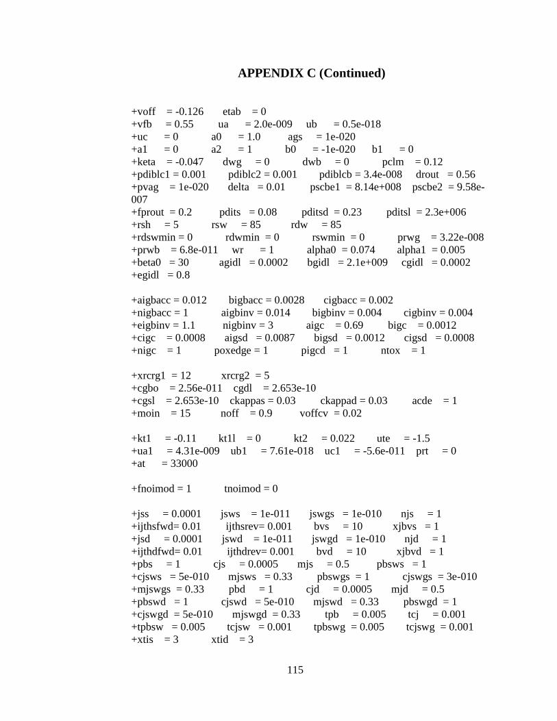
115
APPENDIX C (Continued)
+voff = -0.126 etab = 0
+vfb = 0.55 ua = 2.0e-009 ub = 0.5e-018
+uc = 0 a0 = 1.0 ags = 1e-020
+a1 = 0 a2 = 1 b0 = -1e-020 b1 = 0
+keta = -0.047 dwg = 0 dwb = 0 pclm = 0.12
+pdiblc1 = 0.001 pdiblc2 = 0.001 pdiblcb = 3.4e-008 drout = 0.56
+pvag = 1e-020 delta = 0.01 pscbe1 = 8.14e+008 pscbe2 = 9.58e-
007
+fprout = 0.2 pdits = 0.08 pditsd = 0.23 pditsl = 2.3e+006
+rsh = 5 rsw = 85 rdw = 85
+rdswmin = 0 rdwmin = 0 rswmin = 0 prwg = 3.22e-008
+prwb = 6.8e-011 wr = 1 alpha0 = 0.074 alpha1 = 0.005
+beta0 = 30 agidl = 0.0002 bgidl = 2.1e+009 cgidl = 0.0002
+egidl = 0.8
+aigbacc = 0.012 bigbacc = 0.0028 cigbacc = 0.002
+nigbacc = 1 aigbinv = 0.014 bigbinv = 0.004 cigbinv = 0.004
+eigbinv = 1.1 nigbinv = 3 aigc = 0.69 bigc = 0.0012
+cigc = 0.0008 aigsd = 0.0087 bigsd = 0.0012 cigsd = 0.0008
+nigc = 1 poxedge = 1 pigcd = 1 ntox = 1
+xrcrg1 = 12 xrcrg2 = 5
+cgbo = 2.56e-011 cgdl = 2.653e-10
+cgsl = 2.653e-10 ckappas = 0.03 ckappad = 0.03 acde = 1
+moin = 15 noff = 0.9 voffcv = 0.02
+kt1 = -0.11 kt1l = 0 kt2 = 0.022 ute = -1.5
+ua1 = 4.31e-009 ub1 = 7.61e-018 uc1 = -5.6e-011 prt = 0
+at = 33000
+fnoimod = 1 tnoimod = 0
+jss = 0.0001 jsws = 1e-011 jswgs = 1e-010 njs = 1
+ijthsfwd= 0.01 ijthsrev= 0.001 bvs = 10 xjbvs = 1
+jsd = 0.0001 jswd = 1e-011 jswgd = 1e-010 njd = 1
+ijthdfwd= 0.01 ijthdrev= 0.001 bvd = 10 xjbvd = 1
+pbs = 1 cjs = 0.0005 mjs = 0.5 pbsws = 1
+cjsws = 5e-010 mjsws = 0.33 pbswgs = 1 cjswgs = 3e-010
+mjswgs = 0.33 pbd = 1 cjd = 0.0005 mjd = 0.5
+pbswd = 1 cjswd = 5e-010 mjswd = 0.33 pbswgd = 1
+cjswgd = 5e-010 mjswgd = 0.33 tpb = 0.005 tcj = 0.001
+tpbsw = 0.005 tcjsw = 0.001 tpbswg = 0.005 tcjswg = 0.001
+xtis = 3 xtid = 3

116
APPENDIX C (Continued)
+dmcg = 0e-006 dmci = 0e-006 dmdg = 0e-006 dmcgt = 0e-007
+dwj = 0.0e-008 xgw = 0e-007 xgl = 0e-008
+rshg = 0.4 gbmin = 1e-010 rbpb = 5 rbpd = 15
+rbps = 15 rbdb = 15 rbsb = 15 ngcon = 1
h) 65 nm (Nominal)
* Customized PTM 65nm NMOS
.model N nmos level = 14
+version = 4.0 binunit = 1 paramchk= 1 mobmod = 0
+capmod = 2 igcmod = 1 igbmod = 1 geomod = 1
+diomod = 1 rdsmod = 0 rbodymod= 1 rgatemod= 1
+permod = 1 acnqsmod= 0 trnqsmod= 0
* parameters related to the technology node
+tnom = 27 epsrox = 3.9
+eta0 = 0.0058 nfactor = 1.9 wint = 5e-09
+cgso = 1.5e-10 cgdo = 1.5e-10 xl = -3e-08
* parameters customized by the user
+toxe = 1.85e-09 toxp = 1.2e-09 toxm = 1.85e-09 toxref = 1.85e-09
+dtox = 6.5e-10 lint = -2.5e-09
+vth0 = 0.42 k1 = 0.49 u0 = 0.04926 vsat = 124340
+rdsw = 165 ndep = 2.52e+18 xj = 3.2e-08
* secondary parameters
+ll = 0 wl = 0 lln = 1 wln = 1
+lw = 0 ww = 0 lwn = 1 wwn = 1
+lwl = 0 wwl = 0 xpart = 0
+k2 = 0.01 k3 = 0
+k3b = 0 w0 = 2.5e-006 dvt0 = 1 dvt1 = 2
+dvt2 = -0.032 dvt0w = 0 dvt1w = 0 dvt2w = 0
+dsub = 0.1 minv = 0.05 voffl = 0 dvtp0 = 1.0e-009
+dvtp1 = 0.1 lpe0 = 0 lpeb = 0
+ngate = 2e+020 nsd = 2e+020 phin = 0
+cdsc = 0.000 cdscb = 0 cdscd = 0 cit = 0
+voff = -0.13 etab = 0
+vfb = -0.55 ua = 6e-010 ub = 1.2e-018
+uc = 0 a0 = 1.0 ags = 1e-020
+a1 = 0 a2 = 1.0 b0 = 0 b1 = 0
+keta = 0.04 dwg = 0 dwb = 0 pclm = 0.04
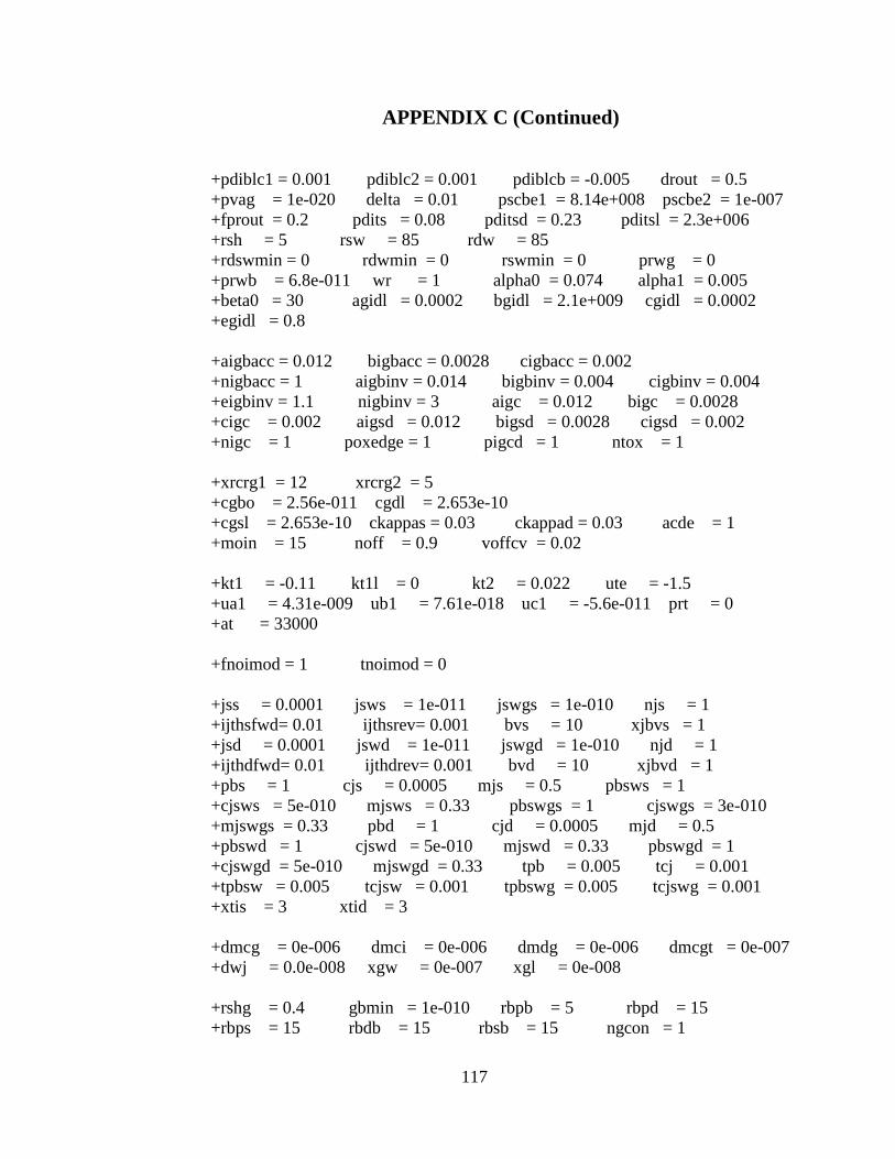
117
APPENDIX C (Continued)
+pdiblc1 = 0.001 pdiblc2 = 0.001 pdiblcb = -0.005 drout = 0.5
+pvag = 1e-020 delta = 0.01 pscbe1 = 8.14e+008 pscbe2 = 1e-007
+fprout = 0.2 pdits = 0.08 pditsd = 0.23 pditsl = 2.3e+006
+rsh = 5 rsw = 85 rdw = 85
+rdswmin = 0 rdwmin = 0 rswmin = 0 prwg = 0
+prwb = 6.8e-011 wr = 1 alpha0 = 0.074 alpha1 = 0.005
+beta0 = 30 agidl = 0.0002 bgidl = 2.1e+009 cgidl = 0.0002
+egidl = 0.8
+aigbacc = 0.012 bigbacc = 0.0028 cigbacc = 0.002
+nigbacc = 1 aigbinv = 0.014 bigbinv = 0.004 cigbinv = 0.004
+eigbinv = 1.1 nigbinv = 3 aigc = 0.012 bigc = 0.0028
+cigc = 0.002 aigsd = 0.012 bigsd = 0.0028 cigsd = 0.002
+nigc = 1 poxedge = 1 pigcd = 1 ntox = 1
+xrcrg1 = 12 xrcrg2 = 5
+cgbo = 2.56e-011 cgdl = 2.653e-10
+cgsl = 2.653e-10 ckappas = 0.03 ckappad = 0.03 acde = 1
+moin = 15 noff = 0.9 voffcv = 0.02
+kt1 = -0.11 kt1l = 0 kt2 = 0.022 ute = -1.5
+ua1 = 4.31e-009 ub1 = 7.61e-018 uc1 = -5.6e-011 prt = 0
+at = 33000
+fnoimod = 1 tnoimod = 0
+jss = 0.0001 jsws = 1e-011 jswgs = 1e-010 njs = 1
+ijthsfwd= 0.01 ijthsrev= 0.001 bvs = 10 xjbvs = 1
+jsd = 0.0001 jswd = 1e-011 jswgd = 1e-010 njd = 1
+ijthdfwd= 0.01 ijthdrev= 0.001 bvd = 10 xjbvd = 1
+pbs = 1 cjs = 0.0005 mjs = 0.5 pbsws = 1
+cjsws = 5e-010 mjsws = 0.33 pbswgs = 1 cjswgs = 3e-010
+mjswgs = 0.33 pbd = 1 cjd = 0.0005 mjd = 0.5
+pbswd = 1 cjswd = 5e-010 mjswd = 0.33 pbswgd = 1
+cjswgd = 5e-010 mjswgd = 0.33 tpb = 0.005 tcj = 0.001
+tpbsw = 0.005 tcjsw = 0.001 tpbswg = 0.005 tcjswg = 0.001
+xtis = 3 xtid = 3
+dmcg = 0e-006 dmci = 0e-006 dmdg = 0e-006 dmcgt = 0e-007
+dwj = 0.0e-008 xgw = 0e-007 xgl = 0e-008
+rshg = 0.4 gbmin = 1e-010 rbpb = 5 rbpd = 15
+rbps = 15 rbdb = 15 rbsb = 15 ngcon = 1

118
APPENDIX C (Continued)
* Customized PTM 65nm PMOS
.model P pmos level = 14
+version = 4.0 binunit = 1 paramchk= 1 mobmod = 0
+capmod = 2 igcmod = 1 igbmod = 1 geomod = 1
+diomod = 1 rdsmod = 0 rbodymod= 1 rgatemod= 1
+permod = 1 acnqsmod= 0 trnqsmod= 0
* parameters related to the technology node
+tnom = 27 epsrox = 3.9
+eta0 = 0.0058 nfactor = 1.9 wint = 5e-09
+cgso = 1.5e-10 cgdo = 1.5e-10 xl = -3e-08
* parameters customized by the user
+toxe = 1.95e-09 toxp = 1.2e-09 toxm = 1.95e-09 toxref = 1.95e-09
+dtox = 7.5e-10 lint = -2.5e-09
+vth0 = -0.36 k1 = 0.441 u0 = 0.00581 vsat = 70000
+rdsw = 165 ndep = 1.84e+18 xj = 3.2e-08
*secondary parameters
+ll = 0 wl = 0 lln = 1 wln = 1
+lw = 0 ww = 0 lwn = 1 wwn = 1
+lwl = 0 wwl = 0 xpart = 0
+k2 = -0.01 k3 = 0
+k3b = 0 w0 = 2.5e-006 dvt0 = 1 dvt1 = 2
+dvt2 = -0.032 dvt0w = 0 dvt1w = 0 dvt2w = 0
+dsub = 0.1 minv = 0.05 voffl = 0 dvtp0 = 1e-009
+dvtp1 = 0.05 lpe0 = 0 lpeb = 0
+ngate = 2e+020 nsd = 2e+020 phin = 0
+cdsc = 0.000 cdscb = 0 cdscd = 0 cit = 0
+voff = -0.126 etab = 0
+vfb = 0.55 ua = 2.0e-009 ub = 0.5e-018
+uc = 0 a0 = 1.0 ags = 1e-020
+a1 = 0 a2 = 1 b0 = -1e-020 b1 = 0
+keta = -0.047 dwg = 0 dwb = 0 pclm = 0.12
+pdiblc1 = 0.001 pdiblc2 = 0.001 pdiblcb = 3.4e-008 drout = 0.56
+pvag = 1e-020 delta = 0.01 pscbe1 = 8.14e+008 pscbe2 = 9.58e-
007
+fprout = 0.2 pdits = 0.08 pditsd = 0.23 pditsl = 2.3e+006
+rsh = 5 rsw = 85 rdw = 85

119
APPENDIX C (Continued)
+rdswmin = 0 rdwmin = 0 rswmin = 0 prwg = 3.22e-008
+prwb = 6.8e-011 wr = 1 alpha0 = 0.074 alpha1 = 0.005
+beta0 = 30 agidl = 0.0002 bgidl = 2.1e+009 cgidl = 0.0002
+egidl = 0.8
+aigbacc = 0.012 bigbacc = 0.0028 cigbacc = 0.002
+nigbacc = 1 aigbinv = 0.014 bigbinv = 0.004 cigbinv = 0.004
+eigbinv = 1.1 nigbinv = 3 aigc = 0.69 bigc = 0.0012
+cigc = 0.0008 aigsd = 0.0087 bigsd = 0.0012 cigsd = 0.0008
+nigc = 1 poxedge = 1 pigcd = 1 ntox = 1
+xrcrg1 = 12 xrcrg2 = 5
+cgbo = 2.56e-011 cgdl = 2.653e-10
+cgsl = 2.653e-10 ckappas = 0.03 ckappad = 0.03 acde = 1
+moin = 15 noff = 0.9 voffcv = 0.02
+kt1 = -0.11 kt1l = 0 kt2 = 0.022 ute = -1.5
+ua1 = 4.31e-009 ub1 = 7.61e-018 uc1 = -5.6e-011 prt = 0
+at = 33000
+fnoimod = 1 tnoimod = 0
+jss = 0.0001 jsws = 1e-011 jswgs = 1e-010 njs = 1
+ijthsfwd= 0.01 ijthsrev= 0.001 bvs = 10 xjbvs = 1
+jsd = 0.0001 jswd = 1e-011 jswgd = 1e-010 njd = 1
+ijthdfwd= 0.01 ijthdrev= 0.001 bvd = 10 xjbvd = 1
+pbs = 1 cjs = 0.0005 mjs = 0.5 pbsws = 1
+cjsws = 5e-010 mjsws = 0.33 pbswgs = 1 cjswgs = 3e-010
+mjswgs = 0.33 pbd = 1 cjd = 0.0005 mjd = 0.5
+pbswd = 1 cjswd = 5e-010 mjswd = 0.33 pbswgd = 1
+cjswgd = 5e-010 mjswgd = 0.33 tpb = 0.005 tcj = 0.001
+tpbsw = 0.005 tcjsw = 0.001 tpbswg = 0.005 tcjswg = 0.001
+xtis = 3 xtid = 3
+dmcg = 0e-006 dmci = 0e-006 dmdg = 0e-006 dmcgt = 0e-007
+dwj = 0.0e-008 xgw = 0e-007 xgl = 0e-008
+rshg = 0.4 gbmin = 1e-010 rbpb = 5 rbpd = 15
+rbps = 15 rbdb = 15 rbsb = 15 ngcon = 1

120
APPENDIX C (Continued)
i) 65 nm (SS)
* Customized PTM 65nm NMOS: ss
.model N nmos level = 14
+version = 4.0 binunit = 1 paramchk= 1 mobmod = 0
+capmod = 2 igcmod = 1 igbmod = 1 geomod = 1
+diomod = 1 rdsmod = 0 rbodymod= 1 rgatemod= 1
+permod = 1 acnqsmod= 0 trnqsmod= 0
* parameters related to the technology node
+tnom = 27 epsrox = 3.9
+eta0 = 0.0058 nfactor = 1.9 wint = 5e-09
+cgso = 1.5e-10 cgdo = 1.5e-10 xl = -3e-08
* parameters customized by the user
+toxe = 1.85e-09 toxp = 1.2e-09 toxm = 1.85e-09 toxref = 1.85e-09
+dtox = 6.5e-10 lint = -4.5e-09
+vth0 = 0.48 k1 = 0.541 u0 = 0.04504 vsat = 124340
+rdsw = 165 ndep = 3.08e+18 xj = 3.52e-08
* secondary parameters
+ll = 0 wl = 0 lln = 1 wln = 1
+lw = 0 ww = 0 lwn = 1 wwn = 1
+lwl = 0 wwl = 0 xpart = 0
+k2 = 0.01 k3 = 0
+k3b = 0 w0 = 2.5e-006 dvt0 = 1 dvt1 = 2
+dvt2 = -0.032 dvt0w = 0 dvt1w = 0 dvt2w = 0
+dsub = 0.1 minv = 0.05 voffl = 0 dvtp0 = 1.0e-009
+dvtp1 = 0.1 lpe0 = 0 lpeb = 0
+ngate = 2e+020 nsd = 2e+020 phin = 0
+cdsc = 0.000 cdscb = 0 cdscd = 0 cit = 0
+voff = -0.13 etab = 0
+vfb = -0.55 ua = 6e-010 ub = 1.2e-018
+uc = 0 a0 = 1.0 ags = 1e-020
+a1 = 0 a2 = 1.0 b0 = 0 b1 = 0
+keta = 0.04 dwg = 0 dwb = 0 pclm = 0.04
+pdiblc1 = 0.001 pdiblc2 = 0.001 pdiblcb = -0.005 drout = 0.5
+pvag = 1e-020 delta = 0.01 pscbe1 = 8.14e+008 pscbe2 = 1e-007
+fprout = 0.2 pdits = 0.08 pditsd = 0.23 pditsl = 2.3e+006
+rsh = 5 rsw = 85 rdw = 85
+rdswmin = 0 rdwmin = 0 rswmin = 0 prwg = 0

121
APPENDIX C (Continued)
+prwb = 6.8e-011 wr = 1 alpha0 = 0.074 alpha1 = 0.005
+beta0 = 30 agidl = 0.0002 bgidl = 2.1e+009 cgidl = 0.0002
+egidl = 0.8
+aigbacc = 0.012 bigbacc = 0.0028 cigbacc = 0.002
+nigbacc = 1 aigbinv = 0.014 bigbinv = 0.004 cigbinv = 0.004
+eigbinv = 1.1 nigbinv = 3 aigc = 0.012 bigc = 0.0028
+cigc = 0.002 aigsd = 0.012 bigsd = 0.0028 cigsd = 0.002
+nigc = 1 poxedge = 1 pigcd = 1 ntox = 1
+xrcrg1 = 12 xrcrg2 = 5
+cgbo = 2.56e-011 cgdl = 2.653e-10
+cgsl = 2.653e-10 ckappas = 0.03 ckappad = 0.03 acde = 1
+moin = 15 noff = 0.9 voffcv = 0.02
+kt1 = -0.11 kt1l = 0 kt2 = 0.022 ute = -1.5
+ua1 = 4.31e-009 ub1 = 7.61e-018 uc1 = -5.6e-011 prt = 0
+at = 33000
+fnoimod = 1 tnoimod = 0
+jss = 0.0001 jsws = 1e-011 jswgs = 1e-010 njs = 1
+ijthsfwd= 0.01 ijthsrev= 0.001 bvs = 10 xjbvs = 1
+jsd = 0.0001 jswd = 1e-011 jswgd = 1e-010 njd = 1
+ijthdfwd= 0.01 ijthdrev= 0.001 bvd = 10 xjbvd = 1
+pbs = 1 cjs = 0.0005 mjs = 0.5 pbsws = 1
+cjsws = 5e-010 mjsws = 0.33 pbswgs = 1 cjswgs = 3e-010
+mjswgs = 0.33 pbd = 1 cjd = 0.0005 mjd = 0.5
+pbswd = 1 cjswd = 5e-010 mjswd = 0.33 pbswgd = 1
+cjswgd = 5e-010 mjswgd = 0.33 tpb = 0.005 tcj = 0.001
+tpbsw = 0.005 tcjsw = 0.001 tpbswg = 0.005 tcjswg = 0.001
+xtis = 3 xtid = 3
+dmcg = 0e-006 dmci = 0e-006 dmdg = 0e-006 dmcgt = 0e-007
+dwj = 0.0e-008 xgw = 0e-007 xgl = 0e-008
+rshg = 0.4 gbmin = 1e-010 rbpb = 5 rbpd = 15
+rbps = 15 rbdb = 15 rbsb = 15 ngcon = 1
* Customized PTM 65nm PMOS: ss
.model P pmos level = 14

122
APPENDIX C (Continued)
+version = 4.0 binunit = 1 paramchk= 1 mobmod = 0
+capmod = 2 igcmod = 1 igbmod = 1 geomod = 1
+diomod = 1 rdsmod = 0 rbodymod= 1 rgatemod= 1
+permod = 1 acnqsmod= 0 trnqsmod= 0
* parameters related to the technology node
+tnom = 27 epsrox = 3.9
+eta0 = 0.0058 nfactor = 1.9 wint = 5e-09
+cgso = 1.5e-10 cgdo = 1.5e-10 xl = -3e-08
* parameters customized by the user
+toxe = 1.95e-09 toxp = 1.2e-09 toxm = 1.95e-09 toxref = 1.95e-09
+dtox = 7.5e-10 lint = -4.5e-09
+vth0 = -0.419 k1 = 0.492 u0 = 0.00478 vsat = 70000
+rdsw = 165 ndep = 2.29e+18 xj = 3.52e-08
*secondary parameters
+ll = 0 wl = 0 lln = 1 wln = 1
+lw = 0 ww = 0 lwn = 1 wwn = 1
+lwl = 0 wwl = 0 xpart = 0
+k2 = -0.01 k3 = 0
+k3b = 0 w0 = 2.5e-006 dvt0 = 1 dvt1 = 2
+dvt2 = -0.032 dvt0w = 0 dvt1w = 0 dvt2w = 0
+dsub = 0.1 minv = 0.05 voffl = 0 dvtp0 = 1e-009
+dvtp1 = 0.05 lpe0 = 0 lpeb = 0
+ngate = 2e+020 nsd = 2e+020 phin = 0
+cdsc = 0.000 cdscb = 0 cdscd = 0 cit = 0
+voff = -0.126 etab = 0
+vfb = 0.55 ua = 2.0e-009 ub = 0.5e-018
+uc = 0 a0 = 1.0 ags = 1e-020
+a1 = 0 a2 = 1 b0 = -1e-020 b1 = 0
+keta = -0.047 dwg = 0 dwb = 0 pclm = 0.12
+pdiblc1 = 0.001 pdiblc2 = 0.001 pdiblcb = 3.4e-008 drout = 0.56
+pvag = 1e-020 delta = 0.01 pscbe1 = 8.14e+008 pscbe2 = 9.58e-
007
+fprout = 0.2 pdits = 0.08 pditsd = 0.23 pditsl = 2.3e+006
+rsh = 5 rsw = 85 rdw = 85
+rdswmin = 0 rdwmin = 0 rswmin = 0 prwg = 3.22e-008
+prwb = 6.8e-011 wr = 1 alpha0 = 0.074 alpha1 = 0.005
+beta0 = 30 agidl = 0.0002 bgidl = 2.1e+009 cgidl = 0.0002
+egidl = 0.8
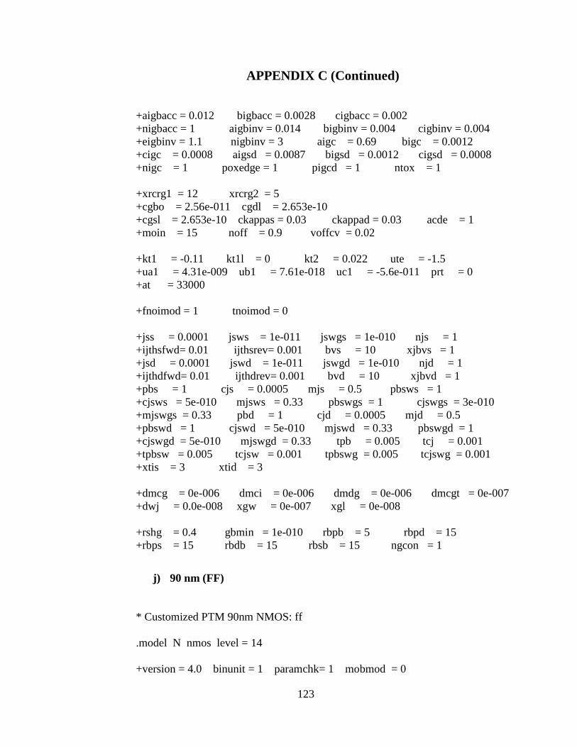
123
APPENDIX C (Continued)
+aigbacc = 0.012 bigbacc = 0.0028 cigbacc = 0.002
+nigbacc = 1 aigbinv = 0.014 bigbinv = 0.004 cigbinv = 0.004
+eigbinv = 1.1 nigbinv = 3 aigc = 0.69 bigc = 0.0012
+cigc = 0.0008 aigsd = 0.0087 bigsd = 0.0012 cigsd = 0.0008
+nigc = 1 poxedge = 1 pigcd = 1 ntox = 1
+xrcrg1 = 12 xrcrg2 = 5
+cgbo = 2.56e-011 cgdl = 2.653e-10
+cgsl = 2.653e-10 ckappas = 0.03 ckappad = 0.03 acde = 1
+moin = 15 noff = 0.9 voffcv = 0.02
+kt1 = -0.11 kt1l = 0 kt2 = 0.022 ute = -1.5
+ua1 = 4.31e-009 ub1 = 7.61e-018 uc1 = -5.6e-011 prt = 0
+at = 33000
+fnoimod = 1 tnoimod = 0
+jss = 0.0001 jsws = 1e-011 jswgs = 1e-010 njs = 1
+ijthsfwd= 0.01 ijthsrev= 0.001 bvs = 10 xjbvs = 1
+jsd = 0.0001 jswd = 1e-011 jswgd = 1e-010 njd = 1
+ijthdfwd= 0.01 ijthdrev= 0.001 bvd = 10 xjbvd = 1
+pbs = 1 cjs = 0.0005 mjs = 0.5 pbsws = 1
+cjsws = 5e-010 mjsws = 0.33 pbswgs = 1 cjswgs = 3e-010
+mjswgs = 0.33 pbd = 1 cjd = 0.0005 mjd = 0.5
+pbswd = 1 cjswd = 5e-010 mjswd = 0.33 pbswgd = 1
+cjswgd = 5e-010 mjswgd = 0.33 tpb = 0.005 tcj = 0.001
+tpbsw = 0.005 tcjsw = 0.001 tpbswg = 0.005 tcjswg = 0.001
+xtis = 3 xtid = 3
+dmcg = 0e-006 dmci = 0e-006 dmdg = 0e-006 dmcgt = 0e-007
+dwj = 0.0e-008 xgw = 0e-007 xgl = 0e-008
+rshg = 0.4 gbmin = 1e-010 rbpb = 5 rbpd = 15
+rbps = 15 rbdb = 15 rbsb = 15 ngcon = 1
j) 90 nm (FF)
* Customized PTM 90nm NMOS: ff
.model N nmos level = 14
+version = 4.0 binunit = 1 paramchk= 1 mobmod = 0
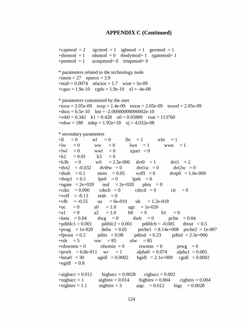
124
APPENDIX C (Continued)
+capmod = 2 igcmod = 1 igbmod = 1 geomod = 1
+diomod = 1 rdsmod = 0 rbodymod= 1 rgatemod= 1
+permod = 1 acnqsmod= 0 trnqsmod= 0
* parameters related to the technology node
+tnom = 27 epsrox = 3.9
+eta0 = 0.0074 nfactor = 1.7 wint = 5e-09
+cgso = 1.9e-10 cgdo = 1.9e-10 xl = -4e-08
* parameters customized by the user
+toxe = 2.05e-09 toxp = 1.4e-09 toxm = 2.05e-09 toxref = 2.05e-09
+dtox = 6.5e-10 lint = -2.00000000000002e-10
+vth0 = 0.342 k1 = 0.428 u0 = 0.05889 vsat = 113760
+rdsw = 180 ndep = 1.92e+18 xj = 4.032e-08
* secondary parameters
+ll = 0 wl = 0 lln = 1 wln = 1
+lw = 0 ww = 0 lwn = 1 wwn = 1
+lwl = 0 wwl = 0 xpart = 0
+k2 = 0.01 k3 = 0
+k3b = 0 w0 = 2.5e-006 dvt0 = 1 dvt1 = 2
+dvt2 = -0.032 dvt0w = 0 dvt1w = 0 dvt2w = 0
+dsub = 0.1 minv = 0.05 voffl = 0 dvtp0 = 1.0e-009
+dvtp1 = 0.1 lpe0 = 0 lpeb = 0
+ngate = 2e+020 nsd = 2e+020 phin = 0
+cdsc = 0.000 cdscb = 0 cdscd = 0 cit = 0
+voff = -0.13 etab = 0
+vfb = -0.55 ua = 6e-010 ub = 1.2e-018
+uc = 0 a0 = 1.0 ags = 1e-020
+a1 = 0 a2 = 1.0 b0 = 0 b1 = 0
+keta = 0.04 dwg = 0 dwb = 0 pclm = 0.04
+pdiblc1 = 0.001 pdiblc2 = 0.001 pdiblcb = -0.005 drout = 0.5
+pvag = 1e-020 delta = 0.01 pscbe1 = 8.14e+008 pscbe2 = 1e-007
+fprout = 0.2 pdits = 0.08 pditsd = 0.23 pditsl = 2.3e+006
+rsh = 5 rsw = 85 rdw = 85
+rdswmin = 0 rdwmin = 0 rswmin = 0 prwg = 0
+prwb = 6.8e-011 wr = 1 alpha0 = 0.074 alpha1 = 0.005
+beta0 = 30 agidl = 0.0002 bgidl = 2.1e+009 cgidl = 0.0002
+egidl = 0.8
+aigbacc = 0.012 bigbacc = 0.0028 cigbacc = 0.002
+nigbacc = 1 aigbinv = 0.014 bigbinv = 0.004 cigbinv = 0.004
+eigbinv = 1.1 nigbinv = 3 aigc = 0.012 bigc = 0.0028

125
APPENDIX C (Continued)
+cigc = 0.002 aigsd = 0.012 bigsd = 0.0028 cigsd = 0.002
+nigc = 1 poxedge = 1 pigcd = 1 ntox = 1
+xrcrg1 = 12 xrcrg2 = 5
+cgbo = 2.56e-011 cgdl = 2.653e-10
+cgsl = 2.653e-10 ckappas = 0.03 ckappad = 0.03 acde = 1
+moin = 15 noff = 0.9 voffcv = 0.02
+kt1 = -0.11 kt1l = 0 kt2 = 0.022 ute = -1.5
+ua1 = 4.31e-009 ub1 = 7.61e-018 uc1 = -5.6e-011 prt = 0
+at = 33000
+fnoimod = 1 tnoimod = 0
+jss = 0.0001 jsws = 1e-011 jswgs = 1e-010 njs = 1
+ijthsfwd= 0.01 ijthsrev= 0.001 bvs = 10 xjbvs = 1
+jsd = 0.0001 jswd = 1e-011 jswgd = 1e-010 njd = 1
+ijthdfwd= 0.01 ijthdrev= 0.001 bvd = 10 xjbvd = 1
+pbs = 1 cjs = 0.0005 mjs = 0.5 pbsws = 1
+cjsws = 5e-010 mjsws = 0.33 pbswgs = 1 cjswgs = 3e-010
+mjswgs = 0.33 pbd = 1 cjd = 0.0005 mjd = 0.5
+pbswd = 1 cjswd = 5e-010 mjswd = 0.33 pbswgd = 1
+cjswgd = 5e-010 mjswgd = 0.33 tpb = 0.005 tcj = 0.001
+tpbsw = 0.005 tcjsw = 0.001 tpbswg = 0.005 tcjswg = 0.001
+xtis = 3 xtid = 3
+dmcg = 0e-006 dmci = 0e-006 dmdg = 0e-006 dmcgt = 0e-007
+dwj = 0.0e-008 xgw = 0e-007 xgl = 0e-008
+rshg = 0.4 gbmin = 1e-010 rbpb = 5 rbpd = 15
+rbps = 15 rbdb = 15 rbsb = 15 ngcon = 1
* Customized PTM 90nm PMOS: ff
.model P pmos level = 14
+version = 4.0 binunit = 1 paramchk= 1 mobmod = 0
+capmod = 2 igcmod = 1 igbmod = 1 geomod = 1
+diomod = 1 rdsmod = 0 rbodymod= 1 rgatemod= 1
+permod = 1 acnqsmod= 0 trnqsmod= 0
* parameters related to the technology node

126
APPENDIX C (Continued)
+tnom = 27 epsrox = 3.9
+eta0 = 0.0074 nfactor = 1.7 wint = 5e-09
+cgso = 1.9e-10 cgdo = 1.9e-10 xl = -4e-08
* parameters customized by the user
+toxe = 2.15e-09 toxp = 1.4e-09 toxm = 2.15e-09 toxref = 2.15e-09
+dtox = 7.5e-10 lint = -2.00000000000002e-10
+vth0 = -0.278 k1 = 0.376 u0 = 0.00854 vsat = 70000
+rdsw = 200 ndep = 1.38e+18 xj = 4.032e-08
*secondary parameters
+ll = 0 wl = 0 lln = 1 wln = 1
+lw = 0 ww = 0 lwn = 1 wwn = 1
+lwl = 0 wwl = 0 xpart = 0
+k2 = -0.01 k3 = 0
+k3b = 0 w0 = 2.5e-006 dvt0 = 1 dvt1 = 2
+dvt2 = -0.032 dvt0w = 0 dvt1w = 0 dvt2w = 0
+dsub = 0.1 minv = 0.05 voffl = 0 dvtp0 = 1e-009
+dvtp1 = 0.05 lpe0 = 0 lpeb = 0
+ngate = 2e+020 nsd = 2e+020 phin = 0
+cdsc = 0.000 cdscb = 0 cdscd = 0 cit = 0
+voff = -0.126 etab = 0
+vfb = 0.55 ua = 2.0e-009 ub = 0.5e-018
+uc = 0 a0 = 1.0 ags = 1e-020
+a1 = 0 a2 = 1 b0 = -1e-020 b1 = 0
+keta = -0.047 dwg = 0 dwb = 0 pclm = 0.12
+pdiblc1 = 0.001 pdiblc2 = 0.001 pdiblcb = 3.4e-008 drout = 0.56
+pvag = 1e-020 delta = 0.01 pscbe1 = 8.14e+008 pscbe2 = 9.58e-
007
+fprout = 0.2 pdits = 0.08 pditsd = 0.23 pditsl = 2.3e+006
+rsh = 5 rsw = 85 rdw = 85
+rdswmin = 0 rdwmin = 0 rswmin = 0 prwg = 3.22e-008
+prwb = 6.8e-011 wr = 1 alpha0 = 0.074 alpha1 = 0.005
+beta0 = 30 agidl = 0.0002 bgidl = 2.1e+009 cgidl = 0.0002
+egidl = 0.8
+aigbacc = 0.012 bigbacc = 0.0028 cigbacc = 0.002
+nigbacc = 1 aigbinv = 0.014 bigbinv = 0.004 cigbinv = 0.004
+eigbinv = 1.1 nigbinv = 3 aigc = 0.69 bigc = 0.0012
+cigc = 0.0008 aigsd = 0.0087 bigsd = 0.0012 cigsd = 0.0008
+nigc = 1 poxedge = 1 pigcd = 1 ntox = 1
+xrcrg1 = 12 xrcrg2 = 5

127
APPENDIX C (Continued)
+cgbo = 2.56e-011 cgdl = 2.653e-10
+cgsl = 2.653e-10 ckappas = 0.03 ckappad = 0.03 acde = 1
+moin = 15 noff = 0.9 voffcv = 0.02
+kt1 = -0.11 kt1l = 0 kt2 = 0.022 ute = -1.5
+ua1 = 4.31e-009 ub1 = 7.61e-018 uc1 = -5.6e-011 prt = 0
+at = 33000
+fnoimod = 1 tnoimod = 0
+jss = 0.0001 jsws = 1e-011 jswgs = 1e-010 njs = 1
+ijthsfwd= 0.01 ijthsrev= 0.001 bvs = 10 xjbvs = 1
+jsd = 0.0001 jswd = 1e-011 jswgd = 1e-010 njd = 1
+ijthdfwd= 0.01 ijthdrev= 0.001 bvd = 10 xjbvd = 1
+pbs = 1 cjs = 0.0005 mjs = 0.5 pbsws = 1
+cjsws = 5e-010 mjsws = 0.33 pbswgs = 1 cjswgs = 3e-010
+mjswgs = 0.33 pbd = 1 cjd = 0.0005 mjd = 0.5
+pbswd = 1 cjswd = 5e-010 mjswd = 0.33 pbswgd = 1
+cjswgd = 5e-010 mjswgd = 0.33 tpb = 0.005 tcj = 0.001
+tpbsw = 0.005 tcjsw = 0.001 tpbswg = 0.005 tcjswg = 0.001
+xtis = 3 xtid = 3
+dmcg = 0e-006 dmci = 0e-006 dmdg = 0e-006 dmcgt = 0e-007
+dwj = 0.0e-008 xgw = 0e-007 xgl = 0e-008
+rshg = 0.4 gbmin = 1e-010 rbpb = 5 rbpd = 15
+rbps = 15 rbdb = 15 rbsb = 15 ngcon = 1
k) 90 nm (Nominal)
* Customized PTM 90nm NMOS
.model N nmos level = 14
+version = 4.0 binunit = 1 paramchk= 1 mobmod = 0
+capmod = 2 igcmod = 1 igbmod = 1 geomod = 1
+diomod = 1 rdsmod = 0 rbodymod= 1 rgatemod= 1
+permod = 1 acnqsmod= 0 trnqsmod= 0
* parameters related to the technology node
+tnom = 27 epsrox = 3.9
+eta0 = 0.0074 nfactor = 1.7 wint = 5e-09

128
APPENDIX C (Continued)
+cgso = 1.9e-10 cgdo = 1.9e-10 xl = -4e-08
* parameters customized by the user
+toxe = 2.05e-09 toxp = 1.4e-09 toxm = 2.05e-09 toxref = 2.05e-09
+dtox = 6.5e-10 lint = -3e-09
+vth0 = 0.394 k1 = 0.473 u0 = 0.05487 vsat = 113760
+rdsw = 180 ndep = 1.92e+18 xj = 4.48e-08
* secondary parameters
+ll = 0 wl = 0 lln = 1 wln = 1
+lw = 0 ww = 0 lwn = 1 wwn = 1
+lwl = 0 wwl = 0 xpart = 0
+k2 = 0.01 k3 = 0
+k3b = 0 w0 = 2.5e-006 dvt0 = 1 dvt1 = 2
+dvt2 = -0.032 dvt0w = 0 dvt1w = 0 dvt2w = 0
+dsub = 0.1 minv = 0.05 voffl = 0 dvtp0 = 1.0e-009
+dvtp1 = 0.1 lpe0 = 0 lpeb = 0
+ngate = 2e+020 nsd = 2e+020 phin = 0
+cdsc = 0.000 cdscb = 0 cdscd = 0 cit = 0
+voff = -0.13 etab = 0
+vfb = -0.55 ua = 6e-010 ub = 1.2e-018
+uc = 0 a0 = 1.0 ags = 1e-020
+a1 = 0 a2 = 1.0 b0 = 0 b1 = 0
+keta = 0.04 dwg = 0 dwb = 0 pclm = 0.04
+pdiblc1 = 0.001 pdiblc2 = 0.001 pdiblcb = -0.005 drout = 0.5
+pvag = 1e-020 delta = 0.01 pscbe1 = 8.14e+008 pscbe2 = 1e-007
+fprout = 0.2 pdits = 0.08 pditsd = 0.23 pditsl = 2.3e+006
+rsh = 5 rsw = 85 rdw = 85
+rdswmin = 0 rdwmin = 0 rswmin = 0 prwg = 0
+prwb = 6.8e-011 wr = 1 alpha0 = 0.074 alpha1 = 0.005
+beta0 = 30 agidl = 0.0002 bgidl = 2.1e+009 cgidl = 0.0002
+egidl = 0.8
+aigbacc = 0.012 bigbacc = 0.0028 cigbacc = 0.002
+nigbacc = 1 aigbinv = 0.014 bigbinv = 0.004 cigbinv = 0.004
+eigbinv = 1.1 nigbinv = 3 aigc = 0.012 bigc = 0.0028
+cigc = 0.002 aigsd = 0.012 bigsd = 0.0028 cigsd = 0.002
+nigc = 1 poxedge = 1 pigcd = 1 ntox = 1
+xrcrg1 = 12 xrcrg2 = 5
+cgbo = 2.56e-011 cgdl = 2.653e-10
+cgsl = 2.653e-10 ckappas = 0.03 ckappad = 0.03 acde = 1
+moin = 15 noff = 0.9 voffcv = 0.02
129
APPENDIX C (Continued)
+kt1 = -0.11 kt1l = 0 kt2 = 0.022 ute = -1.5
+ua1 = 4.31e-009 ub1 = 7.61e-018 uc1 = -5.6e-011 prt = 0
+at = 33000
+fnoimod = 1 tnoimod = 0
+jss = 0.0001 jsws = 1e-011 jswgs = 1e-010 njs = 1
+ijthsfwd= 0.01 ijthsrev= 0.001 bvs = 10 xjbvs = 1
+jsd = 0.0001 jswd = 1e-011 jswgd = 1e-010 njd = 1
+ijthdfwd= 0.01 ijthdrev= 0.001 bvd = 10 xjbvd = 1
+pbs = 1 cjs = 0.0005 mjs = 0.5 pbsws = 1
+cjsws = 5e-010 mjsws = 0.33 pbswgs = 1 cjswgs = 3e-010
+mjswgs = 0.33 pbd = 1 cjd = 0.0005 mjd = 0.5
+pbswd = 1 cjswd = 5e-010 mjswd = 0.33 pbswgd = 1
+cjswgd = 5e-010 mjswgd = 0.33 tpb = 0.005 tcj = 0.001
+tpbsw = 0.005 tcjsw = 0.001 tpbswg = 0.005 tcjswg = 0.001
+xtis = 3 xtid = 3
+dmcg = 0e-006 dmci = 0e-006 dmdg = 0e-006 dmcgt = 0e-007
+dwj = 0.0e-008 xgw = 0e-007 xgl = 0e-008
+rshg = 0.4 gbmin = 1e-010 rbpb = 5 rbpd = 15
+rbps = 15 rbdb = 15 rbsb = 15 ngcon = 1
* Customized PTM 90nm PMOS
.model P pmos level = 14
+version = 4.0 binunit = 1 paramchk= 1 mobmod = 0
+capmod = 2 igcmod = 1 igbmod = 1 geomod = 1
+diomod = 1 rdsmod = 0 rbodymod= 1 rgatemod= 1
+permod = 1 acnqsmod= 0 trnqsmod= 0
* parameters related to the technology node
+tnom = 27 epsrox = 3.9
+eta0 = 0.0074 nfactor = 1.7 wint = 5e-09
+cgso = 1.9e-10 cgdo = 1.9e-10 xl = -4e-08
* parameters customized by the user
+toxe = 2.15e-09 toxp = 1.4e-09 toxm = 2.15e-09 toxref = 2.15e-09
+dtox = 7.5e-10 lint = -3e-09

130
APPENDIX C (Continued)
+vth0 = -0.33 k1 = 0.421 u0 = 0.0073 vsat = 70000
+rdsw = 200 ndep = 1.38e+18 xj = 4.48e-08
*secondary parameters
+ll = 0 wl = 0 lln = 1 wln = 1
+lw = 0 ww = 0 lwn = 1 wwn = 1
+lwl = 0 wwl = 0 xpart = 0
+k2 = -0.01 k3 = 0
+k3b = 0 w0 = 2.5e-006 dvt0 = 1 dvt1 = 2
+dvt2 = -0.032 dvt0w = 0 dvt1w = 0 dvt2w = 0
+dsub = 0.1 minv = 0.05 voffl = 0 dvtp0 = 1e-009
+dvtp1 = 0.05 lpe0 = 0 lpeb = 0
+ngate = 2e+020 nsd = 2e+020 phin = 0
+cdsc = 0.000 cdscb = 0 cdscd = 0 cit = 0
+voff = -0.126 etab = 0
+vfb = 0.55 ua = 2.0e-009 ub = 0.5e-018
+uc = 0 a0 = 1.0 ags = 1e-020
+a1 = 0 a2 = 1 b0 = -1e-020 b1 = 0
+keta = -0.047 dwg = 0 dwb = 0 pclm = 0.12
+pdiblc1 = 0.001 pdiblc2 = 0.001 pdiblcb = 3.4e-008 drout = 0.56
+pvag = 1e-020 delta = 0.01 pscbe1 = 8.14e+008 pscbe2 = 9.58e-
007
+fprout = 0.2 pdits = 0.08 pditsd = 0.23 pditsl = 2.3e+006
+rsh = 5 rsw = 85 rdw = 85
+rdswmin = 0 rdwmin = 0 rswmin = 0 prwg = 3.22e-008
+prwb = 6.8e-011 wr = 1 alpha0 = 0.074 alpha1 = 0.005
+beta0 = 30 agidl = 0.0002 bgidl = 2.1e+009 cgidl = 0.0002
+egidl = 0.8
+aigbacc = 0.012 bigbacc = 0.0028 cigbacc = 0.002
+nigbacc = 1 aigbinv = 0.014 bigbinv = 0.004 cigbinv = 0.004
+eigbinv = 1.1 nigbinv = 3 aigc = 0.69 bigc = 0.0012
+cigc = 0.0008 aigsd = 0.0087 bigsd = 0.0012 cigsd = 0.0008
+nigc = 1 poxedge = 1 pigcd = 1 ntox = 1
+xrcrg1 = 12 xrcrg2 = 5
+cgbo = 2.56e-011 cgdl = 2.653e-10
+cgsl = 2.653e-10 ckappas = 0.03 ckappad = 0.03 acde = 1
+moin = 15 noff = 0.9 voffcv = 0.02
+kt1 = -0.11 kt1l = 0 kt2 = 0.022 ute = -1.5
+ua1 = 4.31e-009 ub1 = 7.61e-018 uc1 = -5.6e-011 prt = 0
+at = 33000

131
APPENDIX C (Continued)
+fnoimod = 1 tnoimod = 0
+jss = 0.0001 jsws = 1e-011 jswgs = 1e-010 njs = 1
+ijthsfwd= 0.01 ijthsrev= 0.001 bvs = 10 xjbvs = 1
+jsd = 0.0001 jswd = 1e-011 jswgd = 1e-010 njd = 1
+ijthdfwd= 0.01 ijthdrev= 0.001 bvd = 10 xjbvd = 1
+pbs = 1 cjs = 0.0005 mjs = 0.5 pbsws = 1
+cjsws = 5e-010 mjsws = 0.33 pbswgs = 1 cjswgs = 3e-010
+mjswgs = 0.33 pbd = 1 cjd = 0.0005 mjd = 0.5
+pbswd = 1 cjswd = 5e-010 mjswd = 0.33 pbswgd = 1
+cjswgd = 5e-010 mjswgd = 0.33 tpb = 0.005 tcj = 0.001
+tpbsw = 0.005 tcjsw = 0.001 tpbswg = 0.005 tcjswg = 0.001
+xtis = 3 xtid = 3
+dmcg = 0e-006 dmci = 0e-006 dmdg = 0e-006 dmcgt = 0e-007
+dwj = 0.0e-008 xgw = 0e-007 xgl = 0e-008
+rshg = 0.4 gbmin = 1e-010 rbpb = 5 rbpd = 15
+rbps = 15 rbdb = 15 rbsb = 15 ngcon = 1
l) 90 nm (SS)
* Customized PTM 90nm NMOS: ss
.model N nmos level = 14
+version = 4.0 binunit = 1 paramchk= 1 mobmod = 0
+capmod = 2 igcmod = 1 igbmod = 1 geomod = 1
+diomod = 1 rdsmod = 0 rbodymod= 1 rgatemod= 1
+permod = 1 acnqsmod= 0 trnqsmod= 0
* parameters related to the technology node
+tnom = 27 epsrox = 3.9
+eta0 = 0.0074 nfactor = 1.7 wint = 5e-09
+cgso = 1.9e-10 cgdo = 1.9e-10 xl = -4e-08
* parameters customized by the user
+toxe = 2.05e-09 toxp = 1.4e-09 toxm = 2.05e-09 toxref = 2.05e-09
+dtox = 6.5e-10 lint = -5.8e-09
+vth0 = 0.444 k1 = 0.517 u0 = 0.05125 vsat = 113760
+rdsw = 180 ndep = 2.29e+18 xj = 4.928e-08
132
APPENDIX C (Continued)
* secondary parameters
+ll = 0 wl = 0 lln = 1 wln = 1
+lw = 0 ww = 0 lwn = 1 wwn = 1
+lwl = 0 wwl = 0 xpart = 0
+k2 = 0.01 k3 = 0
+k3b = 0 w0 = 2.5e-006 dvt0 = 1 dvt1 = 2
+dvt2 = -0.032 dvt0w = 0 dvt1w = 0 dvt2w = 0
+dsub = 0.1 minv = 0.05 voffl = 0 dvtp0 = 1.0e-009
+dvtp1 = 0.1 lpe0 = 0 lpeb = 0
+ngate = 2e+020 nsd = 2e+020 phin = 0
+cdsc = 0.000 cdscb = 0 cdscd = 0 cit = 0
+voff = -0.13 etab = 0
+vfb = -0.55 ua = 6e-010 ub = 1.2e-018
+uc = 0 a0 = 1.0 ags = 1e-020
+a1 = 0 a2 = 1.0 b0 = 0 b1 = 0
+keta = 0.04 dwg = 0 dwb = 0 pclm = 0.04
+pdiblc1 = 0.001 pdiblc2 = 0.001 pdiblcb = -0.005 drout = 0.5
+pvag = 1e-020 delta = 0.01 pscbe1 = 8.14e+008 pscbe2 = 1e-007
+fprout = 0.2 pdits = 0.08 pditsd = 0.23 pditsl = 2.3e+006
+rsh = 5 rsw = 85 rdw = 85
+rdswmin = 0 rdwmin = 0 rswmin = 0 prwg = 0
+prwb = 6.8e-011 wr = 1 alpha0 = 0.074 alpha1 = 0.005
+beta0 = 30 agidl = 0.0002 bgidl = 2.1e+009 cgidl = 0.0002
+egidl = 0.8
+aigbacc = 0.012 bigbacc = 0.0028 cigbacc = 0.002
+nigbacc = 1 aigbinv = 0.014 bigbinv = 0.004 cigbinv = 0.004
+eigbinv = 1.1 nigbinv = 3 aigc = 0.012 bigc = 0.0028
+cigc = 0.002 aigsd = 0.012 bigsd = 0.0028 cigsd = 0.002
+nigc = 1 poxedge = 1 pigcd = 1 ntox = 1
+xrcrg1 = 12 xrcrg2 = 5
+cgbo = 2.56e-011 cgdl = 2.653e-10
+cgsl = 2.653e-10 ckappas = 0.03 ckappad = 0.03 acde = 1
+moin = 15 noff = 0.9 voffcv = 0.02
+kt1 = -0.11 kt1l = 0 kt2 = 0.022 ute = -1.5
+ua1 = 4.31e-009 ub1 = 7.61e-018 uc1 = -5.6e-011 prt = 0
+at = 33000
+fnoimod = 1 tnoimod = 0
+jss = 0.0001 jsws = 1e-011 jswgs = 1e-010 njs = 1

133
APPENDIX C (Continued)
+ijthsfwd= 0.01 ijthsrev= 0.001 bvs = 10 xjbvs = 1
+jsd = 0.0001 jswd = 1e-011 jswgd = 1e-010 njd = 1
+ijthdfwd= 0.01 ijthdrev= 0.001 bvd = 10 xjbvd = 1
+pbs = 1 cjs = 0.0005 mjs = 0.5 pbsws = 1
+cjsws = 5e-010 mjsws = 0.33 pbswgs = 1 cjswgs = 3e-010
+mjswgs = 0.33 pbd = 1 cjd = 0.0005 mjd = 0.5
+pbswd = 1 cjswd = 5e-010 mjswd = 0.33 pbswgd = 1
+cjswgd = 5e-010 mjswgd = 0.33 tpb = 0.005 tcj = 0.001
+tpbsw = 0.005 tcjsw = 0.001 tpbswg = 0.005 tcjswg = 0.001
+xtis = 3 xtid = 3
+dmcg = 0e-006 dmci = 0e-006 dmdg = 0e-006 dmcgt = 0e-007
+dwj = 0.0e-008 xgw = 0e-007 xgl = 0e-008
+rshg = 0.4 gbmin = 1e-010 rbpb = 5 rbpd = 15
+rbps = 15 rbdb = 15 rbsb = 15 ngcon = 1
* Customized PTM 90nm PMOS: ss
.model P pmos level = 14
+version = 4.0 binunit = 1 paramchk= 1 mobmod = 0
+capmod = 2 igcmod = 1 igbmod = 1 geomod = 1
+diomod = 1 rdsmod = 0 rbodymod= 1 rgatemod= 1
+permod = 1 acnqsmod= 0 trnqsmod= 0
* parameters related to the technology node
+tnom = 27 epsrox = 3.9
+eta0 = 0.0074 nfactor = 1.7 wint = 5e-09
+cgso = 1.9e-10 cgdo = 1.9e-10 xl = -4e-08
* parameters customized by the user
+toxe = 2.15e-09 toxp = 1.4e-09 toxm = 2.15e-09 toxref = 2.15e-09
+dtox = 7.5e-10 lint = -5.8e-09
+vth0 = -0.38 k1 = 0.464 u0 = 0.00627 vsat = 70000
+rdsw = 200 ndep = 1.68e+18 xj = 4.928e-08
*secondary parameters
+ll = 0 wl = 0 lln = 1 wln = 1
+lw = 0 ww = 0 lwn = 1 wwn = 1
+lwl = 0 wwl = 0 xpart = 0
+k2 = -0.01 k3 = 0
134
APPENDIX C (Continued)
+k3b = 0 w0 = 2.5e-006 dvt0 = 1 dvt1 = 2
+dvt2 = -0.032 dvt0w = 0 dvt1w = 0 dvt2w = 0
+dsub = 0.1 minv = 0.05 voffl = 0 dvtp0 = 1e-009
+dvtp1 = 0.05 lpe0 = 0 lpeb = 0
+ngate = 2e+020 nsd = 2e+020 phin = 0
+cdsc = 0.000 cdscb = 0 cdscd = 0 cit = 0
+voff = -0.126 etab = 0
+vfb = 0.55 ua = 2.0e-009 ub = 0.5e-018
+uc = 0 a0 = 1.0 ags = 1e-020
+a1 = 0 a2 = 1 b0 = -1e-020 b1 = 0
+keta = -0.047 dwg = 0 dwb = 0 pclm = 0.12
+pdiblc1 = 0.001 pdiblc2 = 0.001 pdiblcb = 3.4e-008 drout = 0.56
+pvag = 1e-020 delta = 0.01 pscbe1 = 8.14e+008 pscbe2 = 9.58e-
007
+fprout = 0.2 pdits = 0.08 pditsd = 0.23 pditsl = 2.3e+006
+rsh = 5 rsw = 85 rdw = 85
+rdswmin = 0 rdwmin = 0 rswmin = 0 prwg = 3.22e-008
+prwb = 6.8e-011 wr = 1 alpha0 = 0.074 alpha1 = 0.005
+beta0 = 30 agidl = 0.0002 bgidl = 2.1e+009 cgidl = 0.0002
+egidl = 0.8
+aigbacc = 0.012 bigbacc = 0.0028 cigbacc = 0.002
+nigbacc = 1 aigbinv = 0.014 bigbinv = 0.004 cigbinv = 0.004
+eigbinv = 1.1 nigbinv = 3 aigc = 0.69 bigc = 0.0012
+cigc = 0.0008 aigsd = 0.0087 bigsd = 0.0012 cigsd = 0.0008
+nigc = 1 poxedge = 1 pigcd = 1 ntox = 1
+xrcrg1 = 12 xrcrg2 = 5
+cgbo = 2.56e-011 cgdl = 2.653e-10
+cgsl = 2.653e-10 ckappas = 0.03 ckappad = 0.03 acde = 1
+moin = 15 noff = 0.9 voffcv = 0.02
+kt1 = -0.11 kt1l = 0 kt2 = 0.022 ute = -1.5
+ua1 = 4.31e-009 ub1 = 7.61e-018 uc1 = -5.6e-011 prt = 0
+at = 33000
+fnoimod = 1 tnoimod = 0
+jss = 0.0001 jsws = 1e-011 jswgs = 1e-010 njs = 1
+ijthsfwd= 0.01 ijthsrev= 0.001 bvs = 10 xjbvs = 1
+jsd = 0.0001 jswd = 1e-011 jswgd = 1e-010 njd = 1
+ijthdfwd= 0.01 ijthdrev= 0.001 bvd = 10 xjbvd = 1
+pbs = 1 cjs = 0.0005 mjs = 0.5 pbsws = 1

135
APPENDIX C (Continued)
+cjsws = 5e-010 mjsws = 0.33 pbswgs = 1 cjswgs = 3e-010
+mjswgs = 0.33 pbd = 1 cjd = 0.0005 mjd = 0.5
+pbswd = 1 cjswd = 5e-010 mjswd = 0.33 pbswgd = 1
+cjswgd = 5e-010 mjswgd = 0.33 tpb = 0.005 tcj = 0.001
+tpbsw = 0.005 tcjsw = 0.001 tpbswg = 0.005 tcjswg = 0.001
+xtis = 3 xtid = 3
+dmcg = 0e-006 dmci = 0e-006 dmdg = 0e-006 dmcgt = 0e-007
+dwj = 0.0e-008 xgw = 0e-007 xgl = 0e-008
+rshg = 0.4 gbmin = 1e-010 rbpb = 5 rbpd = 15
+rbps = 15 rbdb = 15 rbsb = 15 ngcon = 1

136
APPENDIX D: SmartSpice code for Testing
Mnmos A IN Gnd gnd nmos W=0.09U L=0.045U
Rf A B 95K
Vds Vdd Gnd 1.1
Vids Vdd B 0
VIN IN Gnd 1.1
.dc Vds 0 1.1 0.05
.print I(Vids), V(A), I(Rf)
.end
Top Related