


Languages
Pages
Legal


Single-Channel, 16-Bit Current and Voltage Output DAC with Dynamic Power Control and
HART Connectivity Data Sheet AD5758
Rev. A Document Feedback Information furnished by Analog Devices is believed to be accurate and reliable. However, no responsibility is assumed by Analog Devices for its use, nor for any infringements of patents or other rights of third parties that may result from its use. Specifications subject to change without notice. No license is granted by implication or otherwise under any patent or patent rights of Analog Devices. Trademarks and registered trademarks are the property of their respective owners.
One Technology Way, P.O. Box 9106, Norwood, MA 02062-9106, U.S.A. Tel: 781.329.4700 ©2018–2019 Analog Devices, Inc. All rights reserved. Technical Support www.analog.com
FEATURES 16-bit resolution and monotonicity DPC for thermal management Current/voltage output available on a single terminal Current output ranges: 0 mA to 20 mA, 4 mA to 20 mA,
0 mA to 24 mA, ±20 mA, ±24 mA, −1 mA to +22 mA Voltage output ranges (with 20% overrange): 0 V to 5 V,
0 V to 10 V, ±5 V, and ±10 V User-programmable offset and gain Advanced on-chip diagnostics, including a 12-bit ADC On-chip reference Robust architecture, including output fault protection EMC test standards:
IEC 61000-4-6 conducted immunity (10 V, Class A) IEC 61000-4-3 radiated immunity (20 V/m, Class A) IEC 61000-4-2 ESD (±6 kV contact, Class B) IEC 61000-4-4 electrical fast transient (EFT) (±4 kV, Class B) IEC 61000-4-5 surge (±4 kV, Class B)
32-lead, 5 mm × 5 mm LFCSP −40°C to +115°C temperature range
APPLICATIONS Process control Actuator control Channel isolated analog outputs Programmable logic controller (PLC) and distributed control
systems (DCS) applications HART network connectivity
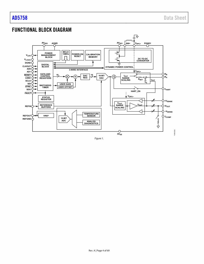
GENERAL DESCRIPTION The AD5758 is a single-channel, voltage and current output digital-to-analog converter (DAC) that operates with a power supply range from −33 V (minimum) on AVSS to +33 V (maximum) on AVDD1 with a maximum operating voltage between the two rails of 60 V. On-chip dynamic power control (DPC) minimizes package power dissipation, which is achieved by regulating the supply voltage (VDPC+) to the VIOUT output driver circuitry from 5 V to 27 V using a buck dc-to-dc
converter, optimized for minimum on-chip power dissipation. The CHART pin enables a HART® signal to be coupled onto the current output.
The device uses a versatile 4-wire serial peripheral interface (SPI) that operates at clock rates of up to 50 MHz and is compatible with standard SPI, QSPI™, MICROWIRE™, DSP, and microcontroller interface standards. The interface also features an optional SPI cyclic redundancy check (CRC) and a watchdog timer (WDT). The AD5758 offers improved diagnostic features from its predecessors, such as an integrated 12-bit diagnostic analog-to-digital converter (ADC). Additional robustness is provided by the inclusion of a line protector on the VIOUT, +VSENSE, and −VSENSE pins. When used with its companion power management unit (PMU)/isolator (ADP1031), the AD5758 is capable of enabling customers to develop an eight channel to channel isolated analog output module with less than 2 W power dissipation, while meeting CISPR 11 Class B.
PRODUCT HIGHLIGHTS 1. DPC, using an integrated buck dc-to-dc converter for
thermal management. When used with the ADP1031, the AD5758 enables eight channel to channel isolated outputs at <2 W dissipated power.
2. Range of advanced diagnostic features, including an integrated ADC for high reliability.
3. Highly robust with output protection from miswire events (±38 V).
4. HART compliant.
COMPANION PRODUCTS
Product Family: AD5755-1, AD5422 Integrated PMU/Isolation: ADP1031 HART Modem: AD5700, AD5700-1 External References: ADR431, ADR3425, ADR4525 Digital Isolators: ADuM142D, ADuM141D Power: LT8300, ADP2360, ADM6339, ADP1031
AD5758 Data Sheet
Rev. A | Page 2 of 69
TABLE OF CONTENTS Features .............................................................................................. 1 Applications ....................................................................................... 1 General Description ......................................................................... 1 Product Highlights ........................................................................... 1 Companion Products ....................................................................... 1 Revision History ............................................................................... 2 Functional Block Diagram .............................................................. 4 Specifications ..................................................................................... 5
AC Performance Characteristics .............................................. 10 Timing Characteristics .............................................................. 11
Absolute Maximum Ratings .......................................................... 14 Thermal Resistance .................................................................... 14 ESD Caution ................................................................................ 14
Pin Configuration and Function Descriptions ........................... 15 Typical Performance Characteristics ........................................... 17
Voltage Output ............................................................................ 17 Current Outputs ......................................................................... 21 DC-to-DC Block ......................................................................... 26 Reference ..................................................................................... 27 General ......................................................................................... 28
Terminology .................................................................................... 29 Theory of Operation ...................................................................... 31
DAC Architecture ....................................................................... 31 Serial Interface ............................................................................ 31 Power-On State of the AD5758 ................................................ 32 Power Supply Considerations ................................................... 32
Device Features and Diagnostics .................................................. 34 Power Dissipation Control ........................................................ 34 Interdie 3-Wire Interface ........................................................... 35
Voltage Output ............................................................................ 36 Fault Protection .......................................................................... 36 Current Output ........................................................................... 36 HART Connectivity ................................................................... 37 Digital Slew Rate Control .......................................................... 37 AD5758 Address Pins ................................................................ 37 Watchdog Timer (WDT) ........................................................... 39 User Digital Offset and Gain Control...................................... 39 DAC Output Update and Data Integrity Diagnostics ........... 40 Use of Key Codes ........................................................................ 41 Software Reset ............................................................................. 41 Calibration Memory CRC ......................................................... 41 Internal Oscillator Diagnostics ................................................. 41 Sticky Diagnostic Results Bits ................................................... 42 Background Supply and Temperature Monitoring ................ 42 Output Fault ................................................................................ 42 ADC Monitoring ........................................................................ 43
Register Map ................................................................................... 46 Writing to Registers ................................................................... 46 Reading from Registers ............................................................. 47 Programming Sequence to Enable the Output ...................... 50 Register Details ........................................................................... 52
Applications Information .............................................................. 67 Example Module Power Calculation ....................................... 67 Driving Inductive Loads ............................................................ 68
Outline Dimensions ....................................................................... 69 Ordering Guide .......................................................................... 69
REVISION HISTORY 3/2019—Rev. 0 to Rev. A Changes to Features Section, General Description Section, Product Highlights Section, and Companion Products Section ................................................................................................ 1 Changes to Figure 1 .......................................................................... 4 Changes to Specifications Section and Table 1 ............................. 5 Added Endnote 4, Table 1; Renumbered Sequentially ................ 7 Changes to AC Performance Characteristics Section and Digital-to-Analog Glitch Energy Parameter, Table 2 ................. 10 Changes to Timing Characteristics Section ................................ 11 Changes to Absolute Maximum Ratings Section and Table 4 .............................................................................................. 14
Added Endnote 2 and Endnote 3, Table 4 ................................... 14 Change to Figure 6 ......................................................................... 15 Changes to Table 6 .......................................................................... 16 Change to Figure 28 ....................................................................... 20 Changes to Figure 34 and Figure 35 ............................................ 21 Changes to Figure 37, Figure 38, Figure 39, Figure 40, Figure 41, and Figure 42 ................................................................................... 22 Changes to Figure 52 and Figure 54 ............................................ 24 Added Figure 53; Renumbered Sequentially .............................. 24 Deleted Figure 71; Renumbered Sequentially ............................ 28 Changes to Theory of Operation Section and Table 7 .............. 31 Changes to Power-On State of the AD5758 Section .................. 32
Data Sheet AD5758
Rev. A | Page 3 of 69
Change to AVDD1 Considerations Section .................................... 32 Change to AVSS Considerations Section ....................................... 33 Changes to Figure 77, Table 10, DPC Current Mode Section, and PPC Current Mode Section ................................................................... 34 Changes to Figure 78 and Fault Protection Section.................... 36 Deleted Internal Current Output Monitor Section and Figure 79; Renumbered Sequentially ............................................ 37 Changes to Figure 79, Digital Slew Rate Control Section, AD5758 Address Pins Section, SPI Interface Diagnostics Section, and Table 12 ...................................................................... 37 Changes to Watchdog Timer (WDT) Section ............................. 39 Change to DAC Output Update and Data Integrity Diagnostics Section .............................................................................................. 40 Changes to Use of Key Codes Section .......................................... 41 Changes to Background Supply and Temperature Monitoring Section .............................................................................................. 42 Changes to Table 17, ADC Monitoring Section, and Table 18 ............................................................................................. 43 Changes to Figure 84 ...................................................................... 44 Changes to ADC Configuration Section, Table 19, and ADC Conversion Timing Section ........................................................... 45 Deleted Key Sequencing (Command 010) Section, Automatic Sequencing (Command 011) Section, Single Immediate Conversion (Command 100) Section, Single Key Conversion (Command 101) Section, Sequencing Mode Setup Section ...... 45 Deleted Table 20; Renumbered Sequentially ............................... 45 Deleted Figure 86 ............................................................................ 46
Changes to Table 20 and Table 21 ................................................. 46 Changes to Table 23 ........................................................................ 47 Changes to Autostatus Readback Mode Section ......................... 48 Changes to Figure 88 ...................................................................... 49 Changes to Programming Sequence to Enable the Output Section .............................................................................................. 50 Changes to Software LDAC Register Section .............................. 55 Changes to Table 34 and Table 35 ................................................. 56 Changes to Table 36 ........................................................................ 57 Changes to DC-to-DC Configuration 1 Register Section, Table 37, and Table 38 ..................................................................... 58 Changes to Table 41 ........................................................................ 61 Changes to Table 42 ........................................................................ 62 Changes to Analog Diagnostic Results Register Section and Table 45 ............................................................................................. 64 Changes to Table 47 ........................................................................ 65 Changes to Power Calculation Methodology (RLOAD = 1 kΩ) Section and Power Calculation Methodology (RLOAD = 0 kΩ) Section .............................................................................................. 67 Added Figure 91 .............................................................................. 68 Changes to Driving Inductive Loads Section .............................. 68 Updated Outline Dimensions ........................................................ 69 Changes to Ordering Guide ........................................................... 69 Deleted Figure 93 ............................................................................ 70 Deleted Figure 94 ............................................................................ 71 5/2018—Revision 0: Initial Version
AD5758 Data Sheet
Rev. A | Page 4 of 69
FUNCTIONAL BLOCK DIAGRAM
AVSS
AGND AVDD1AVDD2
DGND
SCLKSDI
SDO
DC-TO-DCCONVERTER
SYNC
FAULT
DATA ANDCONTROL
REGISTERS
DIGITALBLOCK
WATCHDOGTIMER
STATUSREGISTER
POWER-ONRESET
REFERENCEBUFFERS
DACREG
VREF
CALIBRATIONMEMORY
REFOUT
REFIN
AD1AD0
16-BITDAC
1616
SW+ VDPC+
USER GAINUSER OFFSET
RBRA
IOUTRANGE
SCALING IOUT
DYNAMIC POWER CONTROLCLKOUT
REFGND
POWERMANAGEMENT
BLOCKVLOGIC
VLDO
PGND1
TEMPERATURESENSOR
ANALOGDIAGNOSTICS
12-BITADC
RESET
VDPC+
MCLK10MHz
RSETVX
LDAC
3-WIRE INTERFACE
11840-002
–
HART_EN
VOUTRANGE
SCALING
+VSENSE
VIOUT
–VSENSE
CHART
VOUT
CCOMP
VDPC+
Figure 1.

Data Sheet AD5758
Rev. A | Page 5 of 69
SPECIFICATIONS AVDD1 = VDPC+ = 15 V; dc-to-dc converter disabled; AVDD2 = 5 V; AVSS = −15 V; VLOGIC = 1.71 V to 5.5 V; AGND = DGND = REFGND = PGND1 = 0 V; REFIN = 2.5 V external; voltage output: RL = 1 kΩ, CL = 220 pF; current output: RL = 300 Ω; all specifications at TA = −40°C to +115°C, TJ < 125°C, unless otherwise noted.
Table 1. Parameter Min Typ Max Unit Test Conditions/Comments VOLTAGE OUTPUT
Output Voltage Ranges (VOUT) 0 5 V Trimmed VOUT ranges 0 10 V −5 +5 V −10 +10 V Output Voltage Overranges 0 6 V Untrimmed overranges 0 12 V −6 +6 V −12 +12 V Output Voltage Offset Ranges −0.3 +5.7 V Untrimmed negatively offset ranges −0.4 +11.6 V Resolution 16 Bits
VOLTAGE OUTPUT ACCURACY Loaded and unloaded, accuracy specifications refer to trimmed VOUT ranges only, unless otherwise noted
Total Unadjusted Error (TUE) −0.05 +0.05 % FSR −0.01 +0.01 % FSR TA = 25°C TUE Long-Term Stability1 15 ppm FSR Drift after 1000 hours, TJ = 150°C Output Drift 0.35 2 ppm FSR/°C Output drift Relative Accuracy (INL) −0.006 +0.006 % FSR All ranges Differential Nonlinearity (DNL) −1 +1 LSB Guaranteed monotonic, all ranges Zero-Scale Error −0.02 ±0.002 +0.02 % FSR Zero-Scale Error Temperature
Coefficient (TC) 2 ±0.3 ppm FSR/°C
Bipolar Zero Error −0.015 +0.001 +0.015 % FSR ±5 V, ±10 V Bipolar Zero Error TC2 ±0.3 ppm FSR/°C ±5 V, ±10 V Offset Error −0.02 ±0.002 +0.02 % FSR Offset Error TC2 ±0.3 ppm FSR/°C Gain Error −0.02 ±0.001 +0.02 % FSR Gain Error TC2 ±0.3 ppm FSR/°C Full-Scale Error −0.02 ±0.001 +0.02 % FSR Full-Scale Error TC2 ±0.3 ppm FSR/°C
VOLTAGE OUTPUT CHARACTERISTICS
Headroom 2 V Minimum voltage required between VIOUT and VDPC+ supply
Footroom 2 V Minimum voltage required between VIOUT and AVSS supply
Short-Circuit Current 16 mA Load2 1 kΩ For specified performance Capacitive Load Stability2 10 nF
2 µF External compensation capacitor of 220 pF connected
DC Output Impedance 7 mΩ DC Power Supply Rejection
Ratio (PSRR) 10 µV/V
VOUT/−VSENSE Common-Mode Rejection Ration (CMRR)
10 µV/V Error in VOUT voltage due to changes in −VSENSE voltage
AD5758 Data Sheet
Rev. A | Page 6 of 69
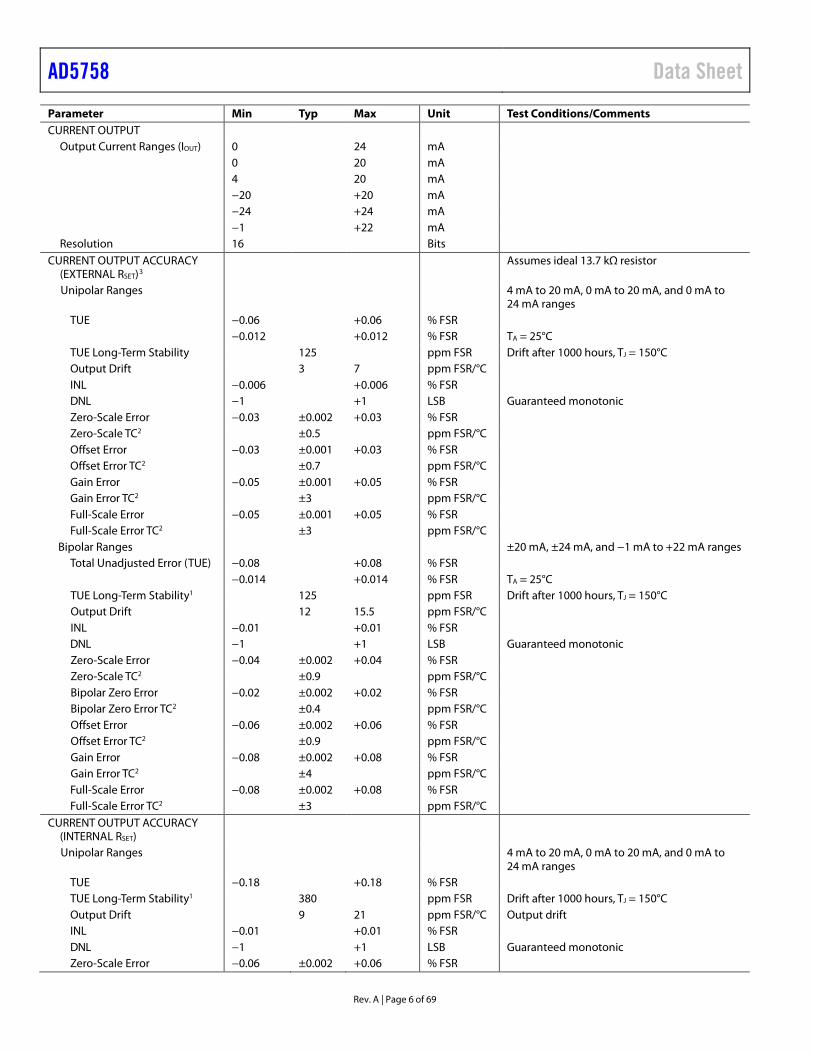
Parameter Min Typ Max Unit Test Conditions/Comments CURRENT OUTPUT
Output Current Ranges (IOUT) 0 24 mA 0 20 mA 4 20 mA −20 +20 mA −24 +24 mA −1 +22 mA
Resolution 16 Bits CURRENT OUTPUT ACCURACY
(EXTERNAL RSET)3 Assumes ideal 13.7 kΩ resistor
Unipolar Ranges 4 mA to 20 mA, 0 mA to 20 mA, and 0 mA to 24 mA ranges
TUE −0.06 +0.06 % FSR −0.012 +0.012 % FSR TA = 25°C TUE Long-Term Stability 125 ppm FSR Drift after 1000 hours, TJ = 150°C Output Drift 3 7 ppm FSR/°C INL −0.006 +0.006 % FSR DNL −1 +1 LSB Guaranteed monotonic Zero-Scale Error −0.03 ±0.002 +0.03 % FSR Zero-Scale TC2 ±0.5 ppm FSR/°C Offset Error −0.03 ±0.001 +0.03 % FSR Offset Error TC2 ±0.7 ppm FSR/°C Gain Error −0.05 ±0.001 +0.05 % FSR Gain Error TC2 ±3 ppm FSR/°C Full-Scale Error −0.05 ±0.001 +0.05 % FSR Full-Scale Error TC2 ±3 ppm FSR/°C
Bipolar Ranges ±20 mA, ±24 mA, and −1 mA to +22 mA ranges Total Unadjusted Error (TUE) −0.08 +0.08 % FSR −0.014 +0.014 % FSR TA = 25°C TUE Long-Term Stability1 125 ppm FSR Drift after 1000 hours, TJ = 150°C Output Drift 12 15.5 ppm FSR/°C INL −0.01 +0.01 % FSR DNL −1 +1 LSB Guaranteed monotonic Zero-Scale Error −0.04 ±0.002 +0.04 % FSR Zero-Scale TC2 ±0.9 ppm FSR/°C Bipolar Zero Error −0.02 ±0.002 +0.02 % FSR Bipolar Zero Error TC2 ±0.4 ppm FSR/°C Offset Error −0.06 ±0.002 +0.06 % FSR Offset Error TC2 ±0.9 ppm FSR/°C Gain Error −0.08 ±0.002 +0.08 % FSR Gain Error TC2 ±4 ppm FSR/°C Full-Scale Error −0.08 ±0.002 +0.08 % FSR Full-Scale Error TC2 ±3 ppm FSR/°C
CURRENT OUTPUT ACCURACY (INTERNAL RSET)
Unipolar Ranges 4 mA to 20 mA, 0 mA to 20 mA, and 0 mA to 24 mA ranges
TUE −0.18 +0.18 % FSR TUE Long-Term Stability1 380 ppm FSR Drift after 1000 hours, TJ = 150°C Output Drift 9 21 ppm FSR/°C Output drift INL −0.01 +0.01 % FSR DNL −1 +1 LSB Guaranteed monotonic Zero-Scale Error −0.06 ±0.002 +0.06 % FSR
Data Sheet AD5758
Rev. A | Page 7 of 69
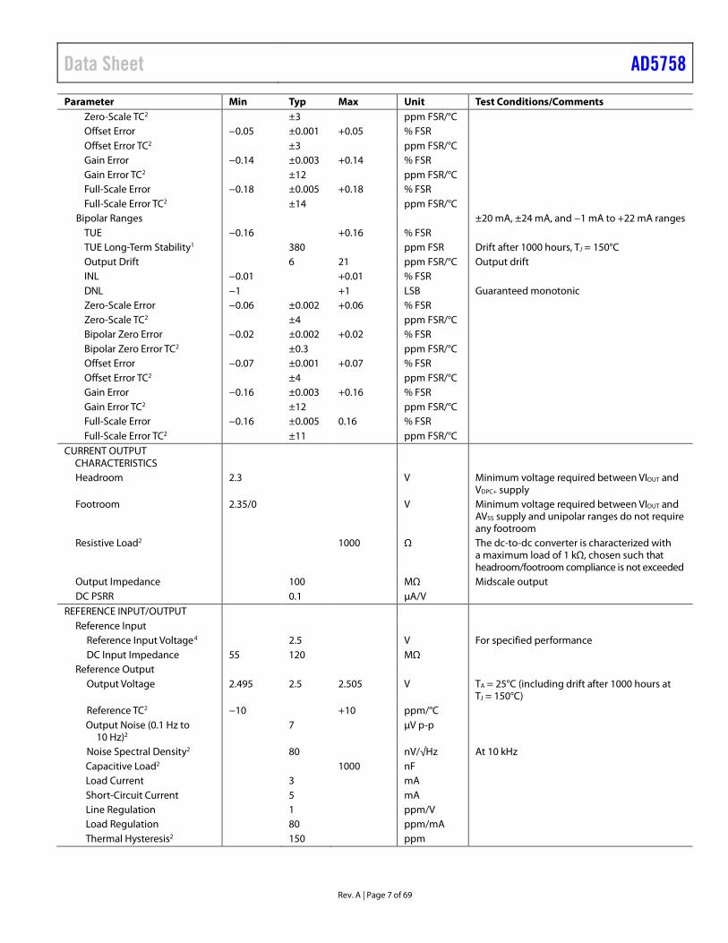
Parameter Min Typ Max Unit Test Conditions/Comments Zero-Scale TC2 ±3 ppm FSR/°C Offset Error −0.05 ±0.001 +0.05 % FSR Offset Error TC2 ±3 ppm FSR/°C Gain Error −0.14 ±0.003 +0.14 % FSR Gain Error TC2 ±12 ppm FSR/°C Full-Scale Error −0.18 ±0.005 +0.18 % FSR Full-Scale Error TC2 ±14 ppm FSR/°C
Bipolar Ranges ±20 mA, ±24 mA, and −1 mA to +22 mA ranges TUE −0.16 +0.16 % FSR TUE Long-Term Stability1 380 ppm FSR Drift after 1000 hours, TJ = 150°C Output Drift 6 21 ppm FSR/°C Output drift INL −0.01 +0.01 % FSR DNL −1 +1 LSB Guaranteed monotonic Zero-Scale Error −0.06 ±0.002 +0.06 % FSR Zero-Scale TC2 ±4 ppm FSR/°C Bipolar Zero Error −0.02 ±0.002 +0.02 % FSR Bipolar Zero Error TC2 ±0.3 ppm FSR/°C Offset Error −0.07 ±0.001 +0.07 % FSR Offset Error TC2 ±4 ppm FSR/°C Gain Error −0.16 ±0.003 +0.16 % FSR Gain Error TC2 ±12 ppm FSR/°C Full-Scale Error −0.16 ±0.005 0.16 % FSR Full-Scale Error TC2 ±11 ppm FSR/°C
CURRENT OUTPUT CHARACTERISTICS
Headroom 2.3 V Minimum voltage required between VIOUT and VDPC+ supply
Footroom 2.35/0 V Minimum voltage required between VIOUT and AVSS supply and unipolar ranges do not require any footroom
Resistive Load2 1000 Ω The dc-to-dc converter is characterized with a maximum load of 1 kΩ, chosen such that headroom/footroom compliance is not exceeded
Output Impedance 100 MΩ Midscale output DC PSRR 0.1 µA/V
REFERENCE INPUT/OUTPUT Reference Input
Reference Input Voltage4 2.5 V For specified performance DC Input Impedance 55 120 MΩ
Reference Output Output Voltage 2.495 2.5 2.505 V TA = 25°C (including drift after 1000 hours at
TJ = 150°C) Reference TC2 −10 +10 ppm/°C Output Noise (0.1 Hz to
10 Hz)2 7 µV p-p
Noise Spectral Density2 80 nV/√Hz At 10 kHz Capacitive Load2 1000 nF Load Current 3 mA Short-Circuit Current 5 mA Line Regulation 1 ppm/V Load Regulation 80 ppm/mA Thermal Hysteresis2 150 ppm

AD5758 Data Sheet
Rev. A | Page 8 of 69
Parameter Min Typ Max Unit Test Conditions/Comments VLDO OUTPUT
Output Voltage 3.3 V Output Voltage TC2 25 ppm/°C Output Voltage Accuracy −2 +2 % Externally Available Current 30 mA Short-Circuit Current 55 mA Load Regulation 0.8 mV/mA Capacitive Load 0.1 µF Recommended operation
DC-TO-DC Start-Up Time 1.25 ms Switch
Peak Current Limit2 150 400 mA User-programmable in 50 mA steps via the DCDC_CONFIG2 register
Oscillator Oscillator Frequency (fSW) 500 kHz Minimum Duty Cycle 5 %
Current Output DPC Mode Current output dynamic power control mode VDPC+ Voltage Range 4.95 27 V Assuming sufficient supply margin between
AVDD1 and VDPC+; see the Power Dissipation Control section for further details; maximum operating range of |VDPC+ to AVSS| = 50 V
VDPC+ Headroom 2.3 2.5 V Typical voltage headroom between VIOUT and VDPC+; only applicable when dc-to-dc converter is in regulation (that is, load is sufficiently high)
Current Output PPC Mode PPC mode VDPC+ Voltage Range 5 25.677 V Assuming sufficient supply margin between
AVDD1 and VDPC+; see the Power Dissipation Control section for further details; maximum operating range of |VDPC+ to AVSS| = 50 V
VDPC+ Voltage Accuracy −500 +500 mV Only applicable when dc-to-dc is operating in regulation (that is, load is sufficiently high)
Voltage Output DPC Mode Voltage output dynamic power control mode VDPC+ Voltage Range 5 15 25 V 5 V = −VSENSE (MIN) + 15 V; 25 V = −VSENSE (MAX) + 15 V;
assuming sufficient supply margin between AVDD1 and VDPC+; see the Power Dissipation Control section for further details; maximum operating range of |VDPC+ to AVSS| = 50 V
VDPC+ Voltage Accuracy −500 +500 mV Only applicable when dc-to-dc is operating in regulation (that is, load sufficiently high)
VIOUT LINE PROTECTOR On Resistance (RON) 12 Ω TA = 25°C Overvoltage Response Time
(tRESPONSE) 250 ns
Overvoltage Leakage Current ±100 µA Line protector fault detect block sinks current for a positive fault and sources current for a negative fault
ADC Resolution 12 Bits Total Error ±0.3 % FSR Table 18 lists all ADC input nodes Conversion Time2 100 µs
DIGITAL INPUTS Input Voltage
3 V ≤ VLOGIC ≤ 5.5 V High, VIH 0.7 × VLOGIC V Low, VIL 0.3 × VLOGIC V
1.71 V ≤ VLOGIC < 3 V
Data Sheet AD5758
Rev. A | Page 9 of 69
Parameter Min Typ Max Unit Test Conditions/Comments High, VIH 0.8 × VLOGIC V Low, VIL 0.2 × VLOGIC V
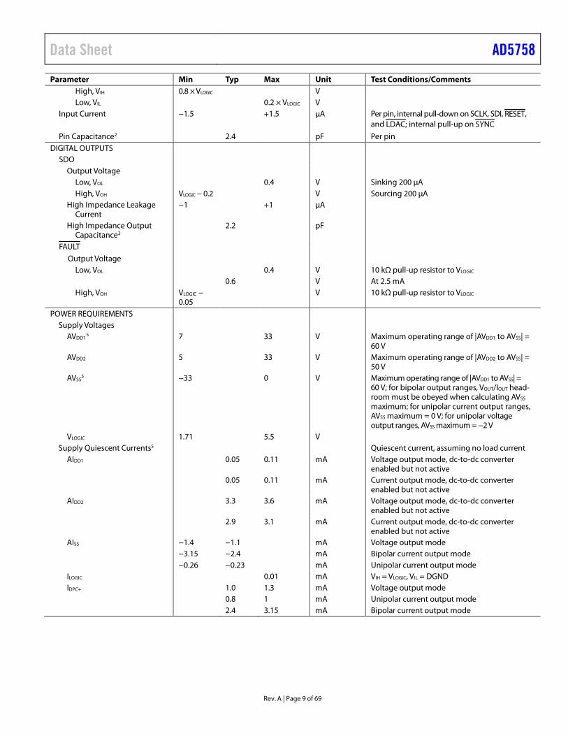
Input Current −1.5 +1.5 µA Per pin, internal pull-down on SCLK, SDI, RESET, and LDAC; internal pull-up on SYNC
Pin Capacitance2 2.4 pF Per pin DIGITAL OUTPUTS
SDO Output Voltage
Low, VOL 0.4 V Sinking 200 µA High, VOH VLOGIC − 0.2 V Sourcing 200 µA
High Impedance Leakage Current
−1 +1 µA
High Impedance Output Capacitance2
2.2 pF
FAULT
Output Voltage Low, VOL 0.4 V 10 kΩ pull-up resistor to VLOGIC 0.6 V At 2.5 mA High, VOH VLOGIC −
0.05 V 10 kΩ pull-up resistor to VLOGIC
POWER REQUIREMENTS Supply Voltages
AVDD15 7 33 V Maximum operating range of |AVDD1 to AVSS| =
60 V AVDD2 5 33 V Maximum operating range of |AVDD2 to AVSS| =
50 V AVSS
5 −33 0 V Maximum operating range of |AVDD1 to AVSS| = 60 V; for bipolar output ranges, VOUT/IOUT head-room must be obeyed when calculating AVSS maximum; for unipolar current output ranges, AVSS maximum = 0 V; for unipolar voltage output ranges, AVSS maximum = −2 V
VLOGIC 1.71 5.5 V Supply Quiescent Currents5 Quiescent current, assuming no load current
AIDD1 0.05 0.11 mA Voltage output mode, dc-to-dc converter enabled but not active
0.05 0.11 mA Current output mode, dc-to-dc converter enabled but not active
AIDD2 3.3 3.6 mA Voltage output mode, dc-to-dc converter enabled but not active
2.9 3.1 mA Current output mode, dc-to-dc converter enabled but not active
AISS −1.4 −1.1 mA Voltage output mode −3.15 −2.4 mA Bipolar current output mode −0.26 −0.23 mA Unipolar current output mode ILOGIC 0.01 mA VIH = VLOGIC, VIL = DGND IDPC+ 1.0 1.3 mA Voltage output mode
0.8 1 mA Unipolar current output mode 2.4 3.15 mA Bipolar current output mode

AD5758 Data Sheet
Rev. A | Page 10 of 69
Parameter Min Typ Max Unit Test Conditions/Comments Power Dissipation Power dissipation assuming an ideal power
supply and excluding external load power dissipation, current output DPC mode, 0 mA to 20 mA range; see the Example Module Power Calculation section for calculation methodology
103 mW AVDD1 = 24 V, AVDD2 = 5 V, AVSS = −15 V, RLOAD = 1 kΩ, IOUT = 20 mA
145 mW AVDD1 = 24 V, AVDD2 = 5 V, AVSS = −15 V, RLOAD = 0 Ω, IOUT = 20 mA
155 mW AVDD1 = AVDD2 = 24 V, AVSS = −15 V, RLOAD = 1 kΩ, IOUT = 20 mA
200 mW AVDD1 = AVDD2 = 24 V, AVSS = −15 V, RLOAD = 0 Ω, IOUT = 20 mA
1 The long-term stability specification is noncumulative. The drift in subsequent 1000 hour periods is significantly lower than in the first 1000 hour period. 2 Guaranteed by design and characterization; not production tested. 3 See the Current Output section for more information about the internal and external RSET resistors. 4 The AD5758 is factory calibrated with an external 2.5 V reference connected to REFIN. 5 Production tested to AVDD1 maximum = 30 V and AVSS minimum = −30 V.
AC PERFORMANCE CHARACTERISTICS AVDD1 = VDPC+ = 15 V; dc-to-dc converter disabled; AVDD2 = 5 V; AVSS = −15 V; VLOGIC = 1.71 V to 5.5 V; AGND = DGND = REFGND = PGND1 = 0 V; REFIN = 2.5 V external; voltage output: RL = 1 kΩ, CL = 220 pF; current output: RL = 300 Ω; all specifications at TA = −40°C to +115°C, TJ < 125°C, unless otherwise noted.
Table 2. Parameter Min Typ Max Unit Test Conditions/Comments DYNAMIC PERFORMANCE1
Voltage Output Output Voltage Settling Time Output voltage settling time specifications also apply for dc-
to-dc converter enabled 6 20 µs 5 V step to ±0.03% FSR, 0 V to 5 V range 12 20 µs 10 V step to ±0.03% FSR, 0 V to 10 V range 15 µs 100 mV step to 1 LSB (16-bit LSB), 0 V to 10 V range Slew Rate 3 V/µs 0 V to 10 V range, digital slew rate control disabled Power-On Glitch Energy 25 nV-sec Digital-to-Analog Glitch Energy 5 nV-sec Glitch Impulse Peak Amplitude 25 mV Digital Feedthrough 2 nV-sec Output Noise (0.1 Hz to 10 Hz
Bandwidth) 0.2 LSB p-p 16-bit LSB, 0 V to 10 V range
Output Noise Spectral Density 185 nV/√Hz Measured at 10 kHz, midscale output, 0 V to 10 V range AC PSRR 70 dB 200 mV, 50 Hz/60 Hz sine wave superimposed on power
supply voltage Current Output
Output Current Settling Time 15 µs To 0.1% FSR (0 mA to 24 mA), dc-to-dc converter disabled 15 µs PPC mode, dc-to-dc converter enabled, dc-to-dc current limit =
150 mA 200 µs DPC mode, dc-to-dc converter enabled; external inductor and
capacitor components as described in Table 10, dc-to-dc current limit = 150 mA.
Output Noise (0.1 Hz to 10 Hz Bandwidth)
0.2 LSB p-p 16-bit LSB, 0 mA to 24 mA range
Output Noise Spectral Density 0.8 nA/√Hz Measured at 10 kHz, midscale output, 0 mA to 24 mA range AC PSRR 80 dB 200 mV, 50 Hz/60 Hz sine wave superimposed on power
supply voltage 1 Guaranteed by design and characterization; not production tested.
Data Sheet AD5758
Rev. A | Page 11 of 69
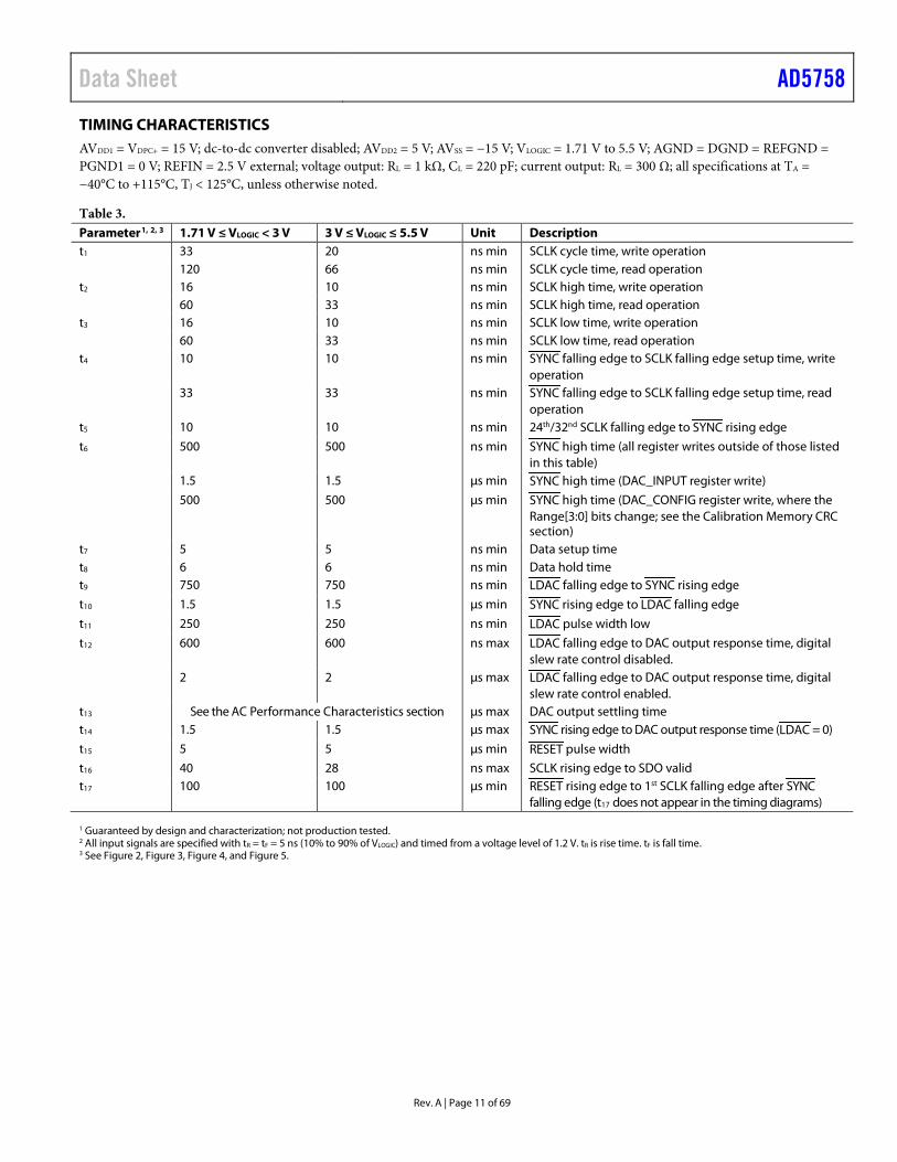
TIMING CHARACTERISTICS AVDD1 = VDPC+ = 15 V; dc-to-dc converter disabled; AVDD2 = 5 V; AVSS = −15 V; VLOGIC = 1.71 V to 5.5 V; AGND = DGND = REFGND = PGND1 = 0 V; REFIN = 2.5 V external; voltage output: RL = 1 kΩ, CL = 220 pF; current output: RL = 300 Ω; all specifications at TA = −40°C to +115°C, TJ < 125°C, unless otherwise noted.
Table 3. Parameter1, 2, 3 1.71 V ≤ VLOGIC < 3 V 3 V ≤ VLOGIC ≤ 5.5 V Unit Description t1 33 20 ns min SCLK cycle time, write operation 120 66 ns min SCLK cycle time, read operation t2 16 10 ns min SCLK high time, write operation 60 33 ns min SCLK high time, read operation t3 16 10 ns min SCLK low time, write operation 60 33 ns min SCLK low time, read operation t4 10 10 ns min SYNC falling edge to SCLK falling edge setup time, write
operation 33 33 ns min SYNC falling edge to SCLK falling edge setup time, read
operation t5 10 10 ns min 24th/32nd SCLK falling edge to SYNC rising edge
t6 500 500 ns min SYNC high time (all register writes outside of those listed in this table)
1.5 1.5 µs min SYNC high time (DAC_INPUT register write)
500 500 µs min SYNC high time (DAC_CONFIG register write, where the Range[3:0] bits change; see the Calibration Memory CRC section)
t7 5 5 ns min Data setup time t8 6 6 ns min Data hold time t9 750 750 ns min LDAC falling edge to SYNC rising edge
t10 1.5 1.5 µs min SYNC rising edge to LDAC falling edge
t11 250 250 ns min LDAC pulse width low
t12 600 600 ns max LDAC falling edge to DAC output response time, digital slew rate control disabled.
2 2 µs max LDAC falling edge to DAC output response time, digital slew rate control enabled.
t13 See the AC Performance Characteristics section µs max DAC output settling time t14 1.5 1.5 µs max SYNC rising edge to DAC output response time (LDAC = 0)
t15 5 5 µs min RESET pulse width
t16 40 28 ns max SCLK rising edge to SDO valid t17 100 100 µs min RESET rising edge to 1st SCLK falling edge after SYNC
falling edge (t17 does not appear in the timing diagrams) 1 Guaranteed by design and characterization; not production tested. 2 All input signals are specified with tR = tF = 5 ns (10% to 90% of VLOGIC) and timed from a voltage level of 1.2 V. tR is rise time. tF is fall time. 3 See Figure 2, Figure 3, Figure 4, and Figure 5.

AD5758 Data Sheet
Rev. A | Page 12 of 69
Timing Diagrams
MSB
SCLK
SYNC
SDI
LDAC
LDAC = 0
1 2 24
LSB
t1
VIOUT
VIOUT
t4
t6 t3 t2
t5
t8t7
t11 t10t11
t12
t13
t13t14
t9
RESET t15
1184
0-00
3
Figure 2. Serial Interface Timing Diagram
SYNC
MSB MSBLSB LSB
INPUT WORD SPECIFIESREGISTER TO BE READ
NOP CONDITION
t6
t16
SDI
MSB LSB
UNDEFINED SELECTED REGISTER DATACLOCKED OUT
SDO
SCLK 24 241 1
1184
0-00
4
Figure 3. Readback Timing Diagram
Data Sheet AD5758
Rev. A | Page 13 of 69
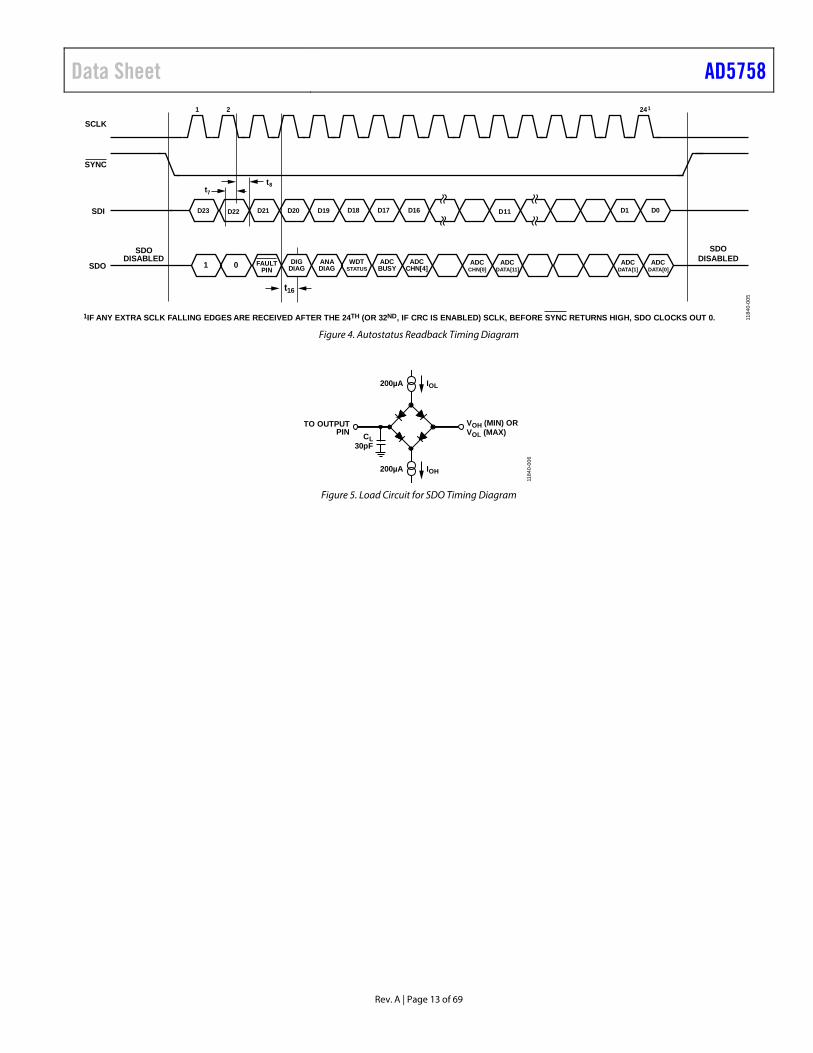
SDODISABLED
SDI
SCLK
SYNC
SDO
1 2 241
D19 D17 D16 D1 D0
ADCBUSY
ADCDATA[1]
ADCDATA[11]
D11
ADCCHN[0]
ADCCHN[4]
WDTSTATUS
D18
ANADIAG
D20D21
FAULTPIN
D22D23
t7t8
SDODISABLED
t16
DIGDIAG1 0 ADC
DATA[0]
1IF ANY EXTRA SCLK FALLING EDGES ARE RECEIVED AFTER THE 24TH (OR 32ND, IF CRC IS ENABLED) SCLK, BEFORE SYNC RETURNS HIGH, SDO CLOCKS OUT 0. 1184
0-00
5
Figure 4. Autostatus Readback Timing Diagram
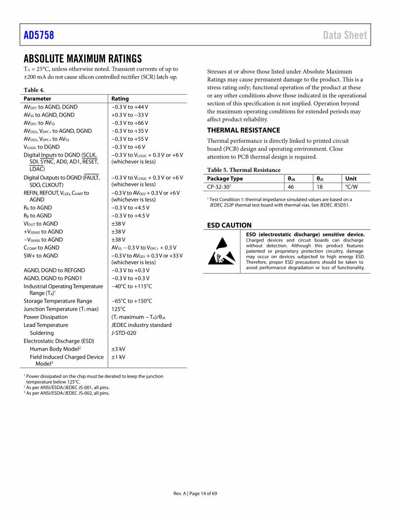
200µA IOL
200µA IOH
VOH (MIN) ORVOL (MAX)
TO OUTPUTPIN CL
30pF
1184
0-00
6
Figure 5. Load Circuit for SDO Timing Diagram
AD5758 Data Sheet
Rev. A | Page 14 of 69
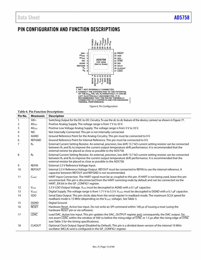
ABSOLUTE MAXIMUM RATINGS TA = 25°C, unless otherwise noted. Transient currents of up to ±200 mA do not cause silicon controlled rectifier (SCR) latch-up.
Table 4. Parameter Rating AVDD1 to AGND, DGND −0.3 V to +44 V AVSS to AGND, DGND +0.3 V to −33 V AVDD1 to AVSS −0.3 V to +66 V AVDD2, VDPC+ to AGND, DGND −0.3 V to +35 V AVDD2, VDPC+ to AVSS −0.3 V to +55 V VLOGIC to DGND −0.3 V to +6 V Digital Inputs to DGND (SCLK,
SDI, SYNC, AD0, AD1, RESET, LDAC)
−0.3 V to VLOGIC + 0.3 V or +6 V (whichever is less)
Digital Outputs to DGND (FAULT, SDO, CLKOUT)
−0.3 V to VLOGIC + 0.3 V or +6 V (whichever is less)
REFIN, REFOUT, VLDO, CHART to AGND
−0.3 V to AVDD2 + 0.3 V or +6 V (whichever is less)
RA to AGND −0.3 V to +4.5 V RB to AGND −0.3 V to +4.5 V VIOUT to AGND ±38 V +VSENSE to AGND ±38 V −VSENSE to AGND ±38 V CCOMP to AGND AVSS − 0.3 V to VDPC+ + 0.3 V SW+ to AGND −0.3 V to AVDD1 + 0.3 V or +33 V
(whichever is less) AGND, DGND to REFGND −0.3 V to +0.3 V AGND, DGND to PGND1 −0.3 V to +0.3 V Industrial Operating Temperature
Range (TA)1 −40°C to +115°C
Storage Temperature Range −65°C to +150°C Junction Temperature (TJ max) 125°C Power Dissipation (TJ maximum − TA)/θJA Lead Temperature JEDEC industry standard
Soldering J-STD-020 Electrostatic Discharge (ESD)
Human Body Model2 ±3 kV Field Induced Charged Device
Model3 ±1 kV
1 Power dissipated on the chip must be derated to keep the junction
temperature below 125°C. 2 As per ANSI/ESDA/JEDEC JS-001, all pins. 3 As per ANSI/ESDA/JEDEC JS-002, all pins.
Stresses at or above those listed under Absolute Maximum Ratings may cause permanent damage to the product. This is a stress rating only; functional operation of the product at these or any other conditions above those indicated in the operational section of this specification is not implied. Operation beyond the maximum operating conditions for extended periods may affect product reliability.
THERMAL RESISTANCE Thermal performance is directly linked to printed circuit board (PCB) design and operating environment. Close attention to PCB thermal design is required.
Table 5. Thermal Resistance Package Type θJA θJC Unit CP-32-301 46 18 °C/W 1 Test Condition 1: thermal impedance simulated values are based on a
JEDEC 2S2P thermal test board with thermal vias. See JEDEC JESD51.
ESD CAUTION
Data Sheet AD5758
Rev. A | Page 15 of 69
PIN CONFIGURATION AND FUNCTION DESCRIPTIONS
24
RESE
T
23 AD0
NOTES1. NIC = NOT INTERNALLY CONNECTED.2. CONNECT THE EXPOSED PAD TO THE POTENTIAL OF THE AVSS PIN, OR, ALTERNATIVELY, IT CAN BE LEFT ELECTRICALLY UNCONNECTED. IT IS RECOMMENDED THAT THE PAD BE THERMALLY CONNECTED TO A COPPER PLANE FOR ENHANCED THERMAL PERFORMANCE.
22 AD1212019
FAULT
18
SYNC
17
SDI
12345678
SW+
NICAGND
REFGND
9 10 11 12 13 14 15 16
REFI
NRE
FOUT
DGND
SDO
SCLKCLKOUT
32 31 30 29 28 27 26 25
PGND
1
NIC
AD5758TOP VIEW
(Not to Scale)
AVDD1AVDD2
RARB
CHA
RT
V LO
GIC
V LDO
AVSS
+VSE
NSE
–VSE
NSE
CCO
MP
VIO
UT
V DPC
+
LDAC
1184
0-00
7
Figure 6. Pin Configuration
Table 6. Pin Function Descriptions Pin No. Mnemonic Description 1 SW+ Switching Output for the DC-to-DC Circuitry. To use the dc-to-dc feature of the device, connect as shown in Figure 77. 2 AVDD1 Positive Analog Supply. The voltage range is from 7 V to 33 V. 3 AVDD2 Positive Low Voltage Analog Supply. The voltage range is from 5 V to 33 V. 4 NIC Not Internally Connected. This pin is not internally connected. 5 AGND Ground Reference Point for the Analog Circuitry. This pin must be connected to 0 V. 6 REFGND Ground Reference Point for Internal Reference. This pin must be connected to 0 V. 7 RA External Current Setting Resistor. An external, precision, low drift 13.7 kΩ current setting resistor can be connected
between RA and RB to improve the current output temperature drift performance. It is recommended that the external resistor be placed as close as possible to the AD5758.
8 RB External Current Setting Resistor. An external, precision, low drift 13.7 kΩ current setting resistor can be connected between RA and RB to improve the current output temperature drift performance. It is recommended that the external resistor be placed as close as possible to the AD5758.
9 REFIN External 2.5 V Reference Voltage Input. 10 REFOUT Internal 2.5 V Reference Voltage Output. REFOUT must be connected to REFIN to use the internal reference. A
capacitor between REFOUT and REFGND is not recommended. 11 CHART HART Input Connection. The HART signal must be ac-coupled to this pin. If HART is not being used, leave this pin
unconnected. This pin is disconnected from the HART summing node by default and can be connected via the HART_EN bit in the GP_CONFIG1 register.
12 VLDO 3.3 V LDO Output Voltage. VLDO must be decoupled to AGND with a 0.1 µF capacitor. 13 VLOGIC Digital Supply. The voltage range is from 1.71 V to 5.5 V. VLOGIC must be decoupled to DGND with a 0.1 µF capacitor. 14 SDO Serial Data Output. This pin clocks data from the serial register in readback mode. The maximum SCLK speed for
readback mode is 15 MHz (depending on the VLOGIC voltage). See Table 3. 15 DGND Digital Ground. 16 RESET Hardware Reset. Active low input. Do not write an SPI command within 100 μs of issuing a reset (using the
hardware RESET pin or via software).
17 LDAC Load DAC. Active low input. This pin updates the DAC_OUTPUT register and, consequently, the DAC output. Do not assert LDAC within the window of 500 ns before the rising edge of SYNC or 1.5 µs after the rising edge of SYNC (see Table 3 for the timing specifications).
18 CLKOUT Optional Clock Output Signal (Disabled by Default). This pin is a divided down version of the internal 10 MHz oscillator (MCLK) and is configured in the GP_CONFIG1 register.
AD5758 Data Sheet
Rev. A | Page 16 of 69
Pin No. Mnemonic Description 19 SCLK Serial Clock Input. Data is clocked into the input shift register on the falling edge of SCLK. In write mode, this pin
operates at clock speeds of up to 50 MHz (depending on the VLOGIC voltage). In read mode, the maximum SCLK speed is 15 MHz (depending on the VLOGIC voltage). See Table 3 for the timing specifications.
20 SDI Serial Data Input. Data must be valid on the falling edge of SCLK. 21 SYNC Frame Synchronization Signal for the Serial Interface. Active low input. While SYNC is low, data is transferred in on
the falling edge of SCLK. 22 AD1 Address Decode 1 for the AD5758. 23 AD0 Address Decode 0 for the AD5758. 24 FAULT Fault Pin. Active low, open-drain output. This pin is high impedance when no faults are detected and is asserted
low when certain faults are detected, for example, an open circuit in current mode, a short circuit in voltage mode, a CRC error, or an overtemperature error (see the Output Fault section). This pin must be connected to VLOGIC with a 10 kΩ pull-up resistor.
25 AVSS Negative Analog Supply. The voltage range is from 0 V to −33 V. If using the device solely for unipolar current output purposes, AVSS can be 0 V. For a unipolar voltage output, AVSS (maximum) is −2.5 V. When using bipolar output ranges, VOUT/IOUT headroom must be obeyed when calculating the AVSS maximum, for example, for a ±10 V output, the AVSS maximum is −12.5 V. See the AVSS Considerations section for an important note on power supply sequencing.
26 −VSENSE Sense Connection for the Negative Voltage Output Load Connection for VOUT Mode. This pin must stay within ±10 V of AGND for specified operation. For specified operation, AVSS tracks −VSENSE with respect to AGND. If remote sensing is not being used, short this pin to AGND.
27 CCOMP Optional Compensation Capacitor Connection for the Voltage Output Buffer. Connecting a 220 pF capacitor between this pin and the VIOUT pin allows the voltage output to drive up to 2 µF. The addition of this capacitor reduces the bandwidth of the output amplifier, increasing the settling time.
28 +VSENSE Sense Connection for the Positive Voltage Output Load Connection for Voltage Output Mode. If remote sensing is not being used, short this pin to VIOUT via a series 1 kΩ resistor.
29 VIOUT Voltage/Current Output Pin. VIOUT is a shared pin, providing either a buffered output voltage or current. 30 NIC Not Internally Connected. This pin is not internally connected. 31 VDPC+ Positive Supply for Current and Voltage Output Stage. To use the dc-to-dc feature of the device, connect as shown
in Figure 77. 32 PGND1 Power Ground. EPAD Exposed Pad. Connect the exposed pad to the potential of the AVSS pin, or, alternatively, it can be left electrically
unconnected. It is recommended that the pad be thermally connected to a copper plane for enhanced thermal performance.

Data Sheet AD5758
Rev. A | Page 17 of 69
TYPICAL PERFORMANCE CHARACTERISTICS VOLTAGE OUTPUT
–0.0015
–0.0010
–0.0005
0
0.0005
0.0010
0.0015
0.0020
0 8192 16384 24576 32768 40960 49152 57344 65536
INL
ERRO
R (%
FSR)
CODE
+5V RANGE+10V RANGE±5V RANGE±10V RANGE+10V RANGE WITH DCDC ENABLED
AVDD1 = VDPC+ = 15VAVSS = –15V1kΩ LOADTA = 25°C
1184
0-20
7
Figure 7. INL Error vs. DAC Code
–1.0
–0.8
–0.6
–0.4
–0.2
0
0.2
0.4
0.6
0.8
1.0
0 8192 16384 24576 32768 40960 49152 57344 65536
DNL
ERRO
R (L
SB)
CODE
+5V RANGE+10V RANGE±5V RANGE±10V RANGE+10V RANGE WITH DCDC ENABLED
AVDD1 = VDPC+ = 15VAVSS = –15V1kΩ LOADTA = 25°C
1184
0-20
8
Figure 8. DNL Error vs. DAC Code
–0.010
–0.008
–0.006
–0.004
–0.002
0
0.002
0.004
0.006
0 8192 16384 24576 32768 40960 49152 57344 65536
TOTA
L UN
ADJU
STED
ERR
OR
(%FS
R)
CODE
+5V RANGE+10V RANGE±5V RANGE±10V RANGE+10V RANGE WITH DC-TO-DC ENABLED
AVDD1 = VDPC+ = 15VAVSS = –15V1kΩ LOADTA = 25°C
1184
0-20
9
Figure 9. Total Unadjusted Error vs. DAC Code
AVDD1 = VDPC+ = 15VAVSS = –15V1kΩ LOAD
–0.0015
–0.0010
–0.0005
0
0.0005
0.0010
0.0015
INL
ERRO
R (%
FSR)
TEMPERATURE (°C) 1184
0-21
0
+5V RANGE, INL MAX+10V RANGE, INL MAX±5V RANGE, INL MAX±10V RANGE, INL MAX
+5V RANGE, INL MIN+10V RANGE, INL MIN±5V RANGE, INL MIN±10V RANGE, INL MIN
–40 25 70 105 125
Figure 10. INL Error vs. Temperature
–1.0
–0.8
–0.6
–0.4
–0.2
0
0.2
0.4
0.6
0.8
1.0
–40 25 115 125
DNL
ERRO
R (L
SB)
TEMPERATURE (ºC)
DNL ERROR MAXDNL ERROR MIN
1 184
0-2 1
1
AVDD1 = VDPC+ = +15VAVSS = –15VALL RANGES
Figure 11. DNL Error vs Temperature
+5V RANGE, TUE MAX+10V RANGE, TUE MAX±5V RANGE, TUE MAX±10V RANGE, TUE MAX
+5V RANGE, TUE MIN+10V RANGE, TUE MIN±5V RANGE, TUE MIN±10V RANGE, TUE MIN
–0.006
–0.004
–0.002
0
0.002
0.004
0.006
0.008
–40 25 70 105 125
TOTA
L UN
ADJU
STED
ERR
OR
(%FS
R)
TEMPERATURE (°C) 1184
0-21
2
AVDD1 = VDPC+ = +15VAVSS = –15V1kΩ LOAD
Figure 12. Total Unadjusted Error vs. Temperature
AD5758 Data Sheet
Rev. A | Page 18 of 69
–0.010
–0.008
–0.006
–0.004
–0.002
0
0.002
0.004
0.006
0.008
–40 25 70 105 125
FULL
-SCA
LE E
RRO
R (%
FSR)
TEMPERATURE (°C)
5V RANGE10V RANGE±5V RANGE±10V RANGE
1184
0-21
4
AVDD1 = VDPC+ = +15VAVSS = –15V1kΩ LOAD
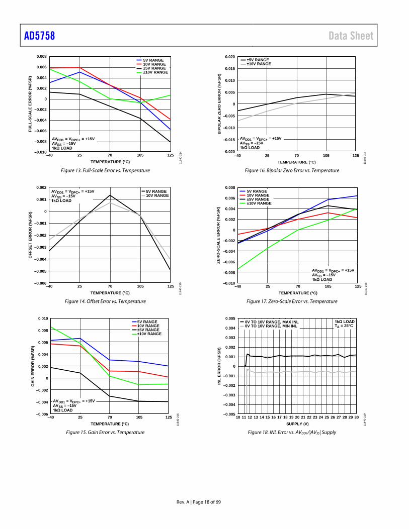
Figure 13. Full-Scale Error vs. Temperature
TEMPERATURE (°C)
–0.006
–0.005
–0.004
–0.003
–0.002
–0.001
0
0.001
0.002
–40 25 70 105 125
OFF
SET
ERRO
R (%
FSR)
5V RANGE10V RANGE
AVDD1 = VDPC+ = +15VAVSS = –15V1kΩ LOAD
1184
0-21
5
Figure 14. Offset Error vs. Temperature
–0.006
–0.004
–0.002
0
0.002
0.004
0.006
0.008
0.010
–40 25 70 105 125
GA
IN E
RR
OR
(%FS
R)
TEMPERATURE (°C)
5V RANGE10V RANGE±5V RANGE±10V RANGE
1184
0-21
6
AVDD1 = VDPC+ = +15VAVSS = –15V1kΩ LOAD
Figure 15. Gain Error vs. Temperature
TEMPERATURE (°C)
–0.020
–0.015
–0.010
–0.005
0
0.005
0.010
0.015
0.020
–40 25 70 105 125
BIPO
LAR
ZERO
ERR
OR
(%FS
R)
±5V RANGE±10V RANGE
1184
0-21
7
AVDD1 = VDPC+ = +15VAVSS = –15V1kΩ LOAD
Figure 16. Bipolar Zero Error vs. Temperature
–0.010
–0.008
–0.006
–0.004
–0.002
0
0.002
0.004
0.006
0.008
–40 25 70 105 125
ZERO
-SCA
LE E
RRO
R (%
FSR)
TEMPERATURE (°C)
5V RANGE10V RANGE±5V RANGE±10V RANGE
1 184
0-21
8
AVDD1 = VDPC+ = +15VAVSS = –15V1kΩ LOAD
Figure 17. Zero-Scale Error vs. Temperature
–0.005
–0.003
–0.001
–0.002
–0.004
0.001
0.002
0
0.004
0.003
0.005
10 11 12 13 14 15 16 17 18 19 20 21 22 23 24 25 26 27 28 29 30
INL
ERRO
R (%
FSR)
SUPPLY (V)
0V TO 10V RANGE, MAX INL0V TO 10V RANGE, MIN INL
1184
0-21
9
1kΩ LOADTA = 25°C
Figure 18. INL Error vs. AVDD1/|AVSS| Supply

Data Sheet AD5758
Rev. A | Page 19 of 69
–1.0
–0.6
–0.2
–0.4
–0.8
0.2
0.4
0
0.8
0.6
1.0
10 11 12 13 14 15 16 17 18 19 20 21 22 23 24 25 26 27 28 29 30
DNL
ERRO
R (%
FSR)
SUPPLY (V)
0V TO 10V RANGE, MAX DNL0V TO 10V RANGE, MIN DNL
1184
0-22
0
1kΩ LOADTA = 25°C
Figure 19. DNL Erorr vs. AVDD1/|AVSS| Supply
–0.05
–0.03
–0.01
–0.02
–0.04
0.01
0.02
0
0.04
0.03
0.05
10 11 12 13 14 15 16 17 18 19 20 21 22 23 24 25 26 27 28 29 30
TOTA
L UN
ADJU
STED
ERR
OR
(%FS
R)
SUPPLY (V)
0V TO 10V RANGE, MAX TUE0V TO 10V RANGE, MIN TUE
1 184
0-22
1
1kΩ LOADTA = 25°C
Figure 20. Total Unadjusted Error vs. AVDD1/|AVSS| Supply
OUTPUT CURRENT (mA)
OUT
PUT
VOLT
AGE
DELT
A (V
)
–0.0010
–0.0006
–0.0002
–0.0004
–0.0008
0.0002
0.0004
0
0.0008
0.0006
0.0010
–20 4–4 8–8 0 12–12–16 16 20
1184
0-22
2
AVDD1 = VDPC+ = +15VAVSS = –15V±10V RANGETA = 25°C
Figure 21. Sink and Source Capability of the Output Amplifier
–15
–10
–5
0
5
10
15
–5 0 5 10 15
OUT
PUT
VOLT
AGE
(V)
TIME (μs)
AVDD1 = VDPC+ = +15VAVSS = –15V±10V RANGEOUTPUT UNLOADEDTA = 25°C
1184
0-22
3
Figure 22. Full-Scale Positive Step
–15
–10
–5
0
5
10
15
–5 0 5 10 15
OUT
PUT
VOLT
AGE
(V)
TIME (μs) 1184
0-22
4
AVDD1 = VDPC+ = +15VAVSS = –15V±10V RANGEOUTPUT UNLOADEDTA = 25°C
Figure 23. Full-Scale Negative Step
–0.025
–0.020
–0.015
–0.010
–0.05
0
0.05
0.10
0 0.5 1.0 1.5 2.0 2.5 3.0 3.5 4.0
V OUT
(V)
TIME (µs)
HIGH TO LOWLOW TO HIGH
1 184
0-22
6
AVDD1 = VDPC+ = +15VAVSS = –15V0 TO 10V RANGE1kΩ LOADTA = 25°C
Figure 24. Digital-to-Analog Glitch Major Code Transition
AD5758 Data Sheet
Rev. A | Page 20 of 69
–15
–10
–5
0
5
10
15
20
0 1 2 3 4 5 6 7 8 9 10
OU
TPU
T VO
LTA
GE
(μV)
TIME (Seconds) 1184
0-22
8
AVDD1 = VDPC+ = +15VAVSS = –15V0V TO 10V RANGEOUTPUT UNLOADED
TA = 25°C
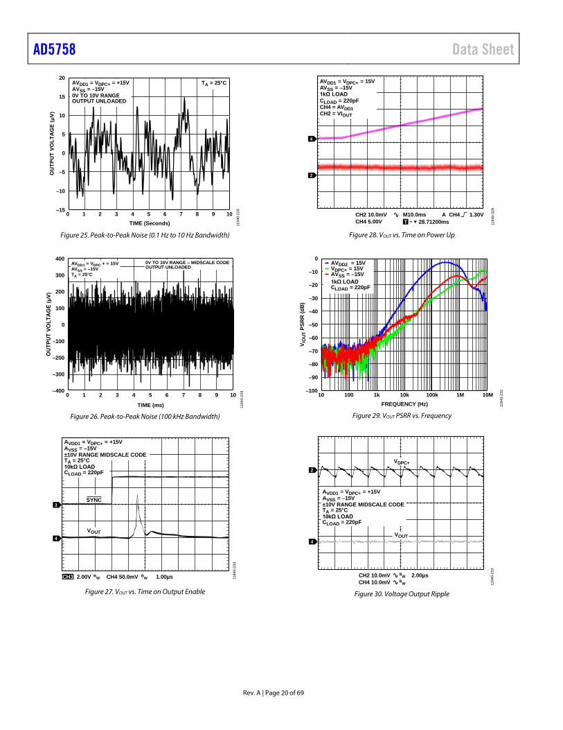
Figure 25. Peak-to-Peak Noise (0.1 Hz to 10 Hz Bandwidth)
–400
–300
–200
–100
0
100
200
300
400
0 1 2 3 4 5 6 7 8 9 10
OUT
PUT
VOLT
AGE
(μV)
TIME (ms)
AVDD1 = VDPC + = 15VAVSS = –15VTA = 25°C
0V TO 10V RANGE – MIDSCALE CODEOUTPUT UNLOADED
1184
0-22
9
Figure 26. Peak-to-Peak Noise (100 kHz Bandwidth)
1.00µs
3
4
CH3 2.00V CH4 50.0mVBW BW 1184
0-23
4
AVDD1 = VDPC+ = +15VAVSS = –15V±10V RANGE MIDSCALE CODETA = 25°C10kΩ LOADCLOAD = 220pF
SYNC
VOUT
Figure 27. VOUT vs. Time on Output Enable
CH2 10.0mV M10.0ms A CH4 1.30V
4
2
T 28.71200msCH4 5.00V
AVDD1 = VDPC+ = 15VAVSS = –15V1kΩ LOADCLOAD = 220pFCH4 = AVDD1CH2 = VIOUT
1184
0-32
8
Figure 28. VOUT vs. Time on Power Up
–100
–90
–80
–70
–60
–50
–40
–30
–20
–10
0
10 100 1k 10k 100k 1M 10M
V IO
UT P
SRR
(dB)
FREQUENCY (Hz)
AVDD2 = 15VVDPC+ = 15VAVSS = –15V1kΩ LOADCLOAD = 220pF
1184
0-23
2
Figure 29. VOUT PSRR vs. Frequency
2.00µs
2
4
CH2 10.0mVCH4 10.0mV BW
BW
1184
0-23
3AVDD1 = VDPC+ = +15VAVSS = –15V±10V RANGE MIDSCALE CODETA = 25°C10kΩ LOADCLOAD = 220pF
VDPC+
VOUT
Figure 30. Voltage Output Ripple

Data Sheet AD5758
Rev. A | Page 21 of 69
CURRENT OUTPUTS
–0.002
–0.001
0
0.001
0.002
0.003
0.004
0 8192 16384 24576 32768 40960 49152 57344 65536
INL
ERRO
R (%
FSR)
CODE
4mA TO 20mA, EXTERNAL RSET4mA TO 20mA, INTERNAL RSET4mA TO 20mA, EXTERNAL RSET, WITH DC-TO-DC CONVERTER4mA TO 20mA, INTERNAL RSET, WITH DC-TO-DC CONVERTER
AVDD = +15VAVSS = –15VTA =25°C300Ω LOAD
1184
0-23
6
Figure 31. INL Error vs. DAC Code
–1.0
–0.8
–0.6
–0.4
–0.2
0
0.2
0.4
0.6
0.8
1.0
0 8192 16384 24576 32768 40960 49152 57344 65536
DNL
ERRO
R (L
SB)
CODE
4mA TO 20mA, EXTERNAL RSET4mA TO 20mA, INTERNAL RSET4mA TO 20mA, EXTERNAL RSET, WITH DC-TO-DC CONVERTER4mA TO 20mA, INTERNAL RSET, WITH DC-TO-DC CONVERTER
1184
0-23
7
Figure 32. DNL Error vs. DAC Code
4mA TO 20mA, EXTERNAL RSET4mA TO 20mA, INTERNAL RSET
–0.020
–0.015
–0.010
–0.005
0
0.005
0.010
0.015
0 8192 16384 24576 32768 40960 49152 57344 65536
TOTA
L UN
ADJU
STED
ERR
OR
(%FS
R)
CODE
4mA TO 20mA, EXTERNAL RSET, WITH DC-TO-DC CONVERTER4mA TO 20mA, INTERNAL RSET, WITH DC-TO-DC CONVERTER
1184
0-23
8
Figure 33. Total Unadjusted Error vs. DAC Code
–05
–0.004
–0.003
–0.002
–0.001
0
0.001
0.002
–40 25 115 125
INL
ERRO
R (%
FSR)
TEMPERATURE (°C)
AVDD1 = +15VAVSS = –15V
0mA TO 20mA, MIN INL0mA TO 24mA, MIN INL4mA TO 20mA, MIN INLp/m 24mA, MIN INL0mA TO 20mA, MAX INL0mA TO 24mA, MAX INL4mA TO 20mA, MAX INLp/m 24mA, MAX INL
1184
0-43
4
Figure 34. INL Error vs. Temperature, Internal RSET
–0.004
–0.003
–0.002
–0.001
0
0.001
0.002
–40 25 115 125
INL
ERRO
R (%
FSR)
AVDD1 = +15VAVSS = –15V
0mA TO 20mA, MAX INL0mA TO 24mA, MAX INL4mA TO 20mA, MAX INLp/m 24mA, MAX INL
0mA TO 20mA, MIN INL0mA TO 24mA, MIN INL4mA TO 20mA, MIN INLp/m 24mA, MIN INL
TEMPERATURE (°C) 1184
0-43
5
Figure 35. INL Error vs. Temperature, External RSET
–0.002
–0.001
0
0.001
0.002
0.003
0.004
0 8192 16384 24576 32768 40960 49152 57344 65536
INL
ERRO
R (%
FSR)
CODE
4mA TO 20mA, EXTERNAL RSET4mA TO 20mA, INTERNAL RSET4mA TO 20mA, EXTERNAL RSET, WITH DC-TO-DC CONVERTER4mA TO 20mA, INTERNAL RSET, WITH DC-TO-DC CONVERTER
AVDD = +15VAVSS = –15VTA =25°C300Ω LOAD
1184
0-33
6
Figure 36. DNL vs. Temperature
AD5758 Data Sheet
Rev. A | Page 22 of 69
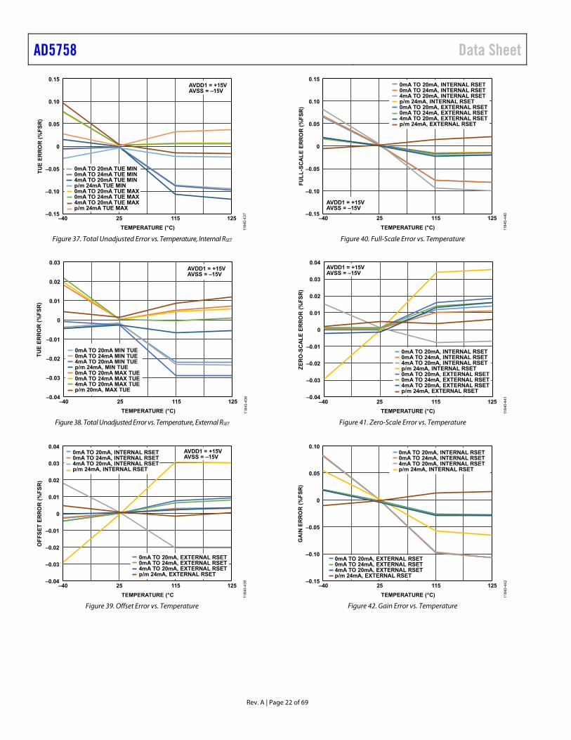
–0.15
–0.10
–0.05
0
0.05
0.10
0.15
–40 25 115 125
TUE
ERRO
R (%
FSR)
TEMPERATURE (°C)
0mA TO 20mA TUE MIN0mA TO 24mA TUE MIN4mA TO 20mA TUE MINp/m 24mA TUE MIN0mA TO 20mA TUE MAX0mA TO 24mA TUE MAX4mA TO 20mA TUE MAXp/m 24mA TUE MAX
AVDD1 = +15VAVSS = –15V
11840-437
Figure 37. Total Unadjusted Error vs. Temperature, Internal RSET
–40 25 115 125–0.04
–0.03
–0.02
–0.01
0
0.01
0.02
0.03
TUE
ERR
OR
(%FS
R)
AVDD1 = +15VAVSS = –15V
TEMPERATURE (°C)
0mA TO 20mA MIN TUE0mA TO 24mA MIN TUE4mA TO 20mA MIN TUEp/m 24mA, MIN TUE0mA TO 20mA MAX TUE0mA TO 24mA MAX TUE4mA TO 20mA MAX TUEp/m 20mA, MAX TUE
11840-438
Figure 38. Total Unadjusted Error vs. Temperature, External RSET
–0.04
–0.03
–0.02
–0.01
0
0.01
0.02
0.03
0.04
–40 25 115 125
OFF
SET
ERRO
R (%
FSR)
TEMPERATURE (°C
0mA TO 20mA, INTERNAL RSET0mA TO 24mA, INTERNAL RSET4mA TO 20mA, INTERNAL RSETp/m 24mA, INTERNAL RSET
0mA TO 20mA, EXTERNAL RSET0mA TO 24mA, EXTERNAL RSET4mA TO 20mA, EXTERNAL RSETp/m 24mA, EXTERNAL RSET
AVDD1 = +15VAVSS = –15V
11840-439
Figure 39. Offset Error vs. Temperature
–40 25 115 125–0.15
–0.10
–0.05
0
0.05
0.10
0.150mA TO 20mA, INTERNAL RSET0mA TO 24mA, INTERNAL RSET4mA TO 20mA, INTERNAL RSETp/m 24mA, INTERNAL RSET0mA TO 20mA, EXTERNAL RSET0mA TO 24mA, EXTERNAL RSET4mA TO 20mA, EXTERNAL RSETp/m 24mA, EXTERNAL RSET
AVDD1 = +15VAVSS = –15V
TEMPERATURE (°C)
FULL
-SCA
LE E
RRO
R (%
FSR)
11840-440
Figure 40. Full-Scale Error vs. Temperature
–0.04
–0.03
–0.02
–0.01
0
0.01
0.02
0.03
0.04
ZERO
-SCA
LE E
RRO
R (%
FSR)
0mA TO 20mA, INTERNAL RSET0mA TO 24mA, INTERNAL RSET4mA TO 20mA, INTERNAL RSETp/m 24mA, INTERNAL RSET0mA TO 20mA, EXTERNAL RSET0mA TO 24mA, EXTERNAL RSET4mA TO 20mA, EXTERNAL RSETp/m 24mA, EXTERNAL RSET
–40 25 115 125TEMPERATURE (°C)
AVDD1 = +15VAVSS = –15V
11840-441
Figure 41. Zero-Scale Error vs. Temperature
–0.15
–0.10
–0.05
0
0.05
0.10
–40 25 115 125
GAI
N ER
ROR
(%FS
R)
0mA TO 20mA, INTERNAL RSET0mA TO 24mA, INTERNAL RSET4mA TO 20mA, INTERNAL RSETp/m 24mA, INTERNAL RSET
0mA TO 20mA, EXTERNAL RSET0mA TO 24mA, EXTERNAL RSET4mA TO 20mA, EXTERNAL RSETp/m 24mA, EXTERNAL RSET
TEMPERATURE (°C) 11840-442
Figure 42. Gain Error vs. Temperature

Data Sheet AD5758
Rev. A | Page 23 of 69
–0.05
–0.04
–0.03
–0.02
–0.01
0
0.01
0.02
0.03
0.04
0.05
6 8 10 12 14 16 18 20 22 24 26 28 30
TUE
ERRO
R (%
FSR)
SUPPLY (V)
4mA TO 20mA RANGE MAX TUE4mA TO 20mA RANGE MIN TUE
RLOAD = 300ΩTA = 25°C
1184
0-26
6
Figure 43. Total Unadjusted Error vs. AVDD1/|AVSS| Supply, Internal RSET
–0.05
–0.04
–0.03
–0.02
–0.01
0
0.01
0.02
0.03
0.04
0.05
TUE
ERRO
R (%
FSR)
SUPPLY (V)6 8 10 12 14 16 18 20 22 24 26 28 30
4mA TO 20mA RANGE MAX TUE4mA TO 20mA RANGE MIN TUE
RLOAD = 300ΩTA = 25°C
1184
0-26
9
Figure 44. Total Unadjusted Error vs. AVDD1/|AVSS| Supply, External RSET
–1.0
–0.8
–0.6
–0.4
–0.2
0
0.2
0.4
0.6
0.8
1.0
6 8 10 12 14 16 18 20 22 24 26 28 30
DN
L ER
RO
R (L
SB)
SUPPLY (V)
4mA TO 20mA RANGE MAX DNL4mA TO 20mA RANGE MIN DNL
LOADA
1184
0-26
4
Figure 45. DNL Error vs. AVDD1/|AVSS| Supply, Internal RSET
–1.0
–0.8
–0.6
–0.4
–0.2
0
0.2
0.4
0.6
0.8
1.0
6 8 10 12 14 16 18 20 22 24 26 28 30
DNL
ERRO
R (L
SB)
SUPPLY (V)
4mA TO 20mA RANGE MAX DNL4mA TO 20mA RANGE MIN DNL
RLOAD = 300ΩTA = 25°C
1184
0-26
7
Figure 46. DNL Error vs. AVDD1/|AVSS| Supply, External RSET
6 8 10 12 14 16 18 20 22 24 26 28 30–0.005
–0.003
–0.001
0.001
0
0.003
0.005
INL
ERRO
R (%
FSR)
SUPPLY (V)
4mA TO 20mA RANGE MAX INL4mA TO 20mA RANGE MIN INL
RLOAD = 300ΩTA = 25°C
1184
0-26
5
Figure 47. INL Error vs. AVDD1/|AVSS| Supply, Internal RSET
6 8 10 12 14 16 18 20 22 24 26 28 30–0.005
–0.003
–0.001
0.001
0.003
0.005
INL
ERRO
R (%
FSR)
SUPPLY (V)
4mA TO 20mA RANGE MAX INL4mA TO 20mA RANGE MIN INL
RLOAD = 300ΩTA = 25°C
1184
0-26
8
Figure 48. INL Error vs. AVDD1/|AVSS| Supply, External RSET

AD5758 Data Sheet
Rev. A | Page 24 of 69
4.00ms
3
4
CH3 5.00V CH4 10.0mVBW BW 1184
0-26
1
IOUT
AVDD1
Figure 49. Output Current vs. Time on Power-Up
400ns
3
4
CH3 2.00V CH4 20.0mVBW BW 1184
0-26
0
TA = 25°C
SYNC
IOUT
Figure 50. Output Current vs. Time on Output Enable
0
2
4
6
8
10
12
14
16
0 5 10 15 20 25 30
HEAD
ROO
M (V
)
OUTPUT CURRENT (mA) 1184
0-25
7
AVDD1 = +30VAVSS = –15V0mA TO 24mA RANGE1kΩ LOADTA = 25°C
Figure 51. DC-to-DC Converter Headroom vs. Output Current
AVDD1 = +15VAVSS = –15V4mA TO 20mA RANGEFULL-SCALE STEP300Ω LOADTA = 25°C
1184
0-23
1–100 –50 0 50 100 150 200 250 300 350 400 450 500
VOLT
AGE
(V)
TIME (µs)
IOUT WITH 150mA LIMIT (V)VDPC+WITH 150mA LIMIT (V)VDPC+ WITH 400mA LIMIT (V)IOUT WITH 400mA LIMIT (V)
Figure 52. Output Current and VDPC+ Settling Time 300 Ω Load
TIME (µs) 1184
0-55
3
–6000
5
10
15
20
25
30
VOLT
AGE
(V)
600 800 1000 1200 1400–400 400–200 2000
VDPC+IOUT
AVDD1 = +24VAVSS = –24V4mA TO 20mA RANGEFULL-SCALE STEP1KΩ LOADTA = 25°C
Figure 53. Output Current and VDPC+ Settling Time 1 kΩ Load
10
9
8
7
6
5
4
3
2
1
0–100 150 200
TIME (µs)250 300 350 400 450 500100–50 500 550
VOLT
AGE
(V)
AVDD1 = +15VAVSS = –15V4mA TO 20mA RANGEFULL-SCALE STEP300Ω LOADDCDCILIMIT = 150mA
IOUT AT –40°CIOUT AT +25°CIOUT AT +85°CIOUT AT +125°C
VDPC+ AT –40°CVDPC+ AT +25°CVDPC+ AT +85°CVDPC+ AT +125°C
1184
0-45
3
Figure 54. Output Current and VDPC+ Settling Time vs. Temperature

Data Sheet AD5758
Rev. A | Page 25 of 69
2.00µs
3
2
4
CH3 2.00V CH2 10.0mVBW BWCH4 10.0mV BW 11
840-
365
Figure 55. Output Current Ripple vs. Time with DC-to-DC Converter
–120
–100
–80
–60
–40
–20
0
20
10 100 1k 10k 100k 1M 10M
I OUT
PSR
R (d
B)
FREQUENCY (Hz)
AVDD2VDPC+AVSS
1184
0-25
6
TA = 25°C
Figure 56. IOUT PSRR vs. Frequency
AD5758 Data Sheet
Rev. A | Page 26 of 69
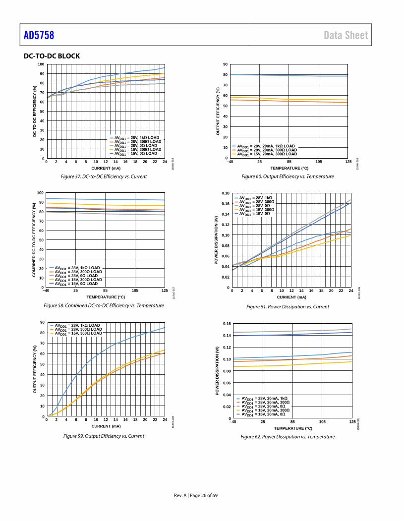
DC-TO-DC BLOCK
0
10
20
30
40
50
60
70
80
90
100
0 2 4 6 8 10 12 14 16 18 20 22 24
DC-T
O-D
C EF
FICI
ENCY
(%)
CURRENT (mA)
AVDD1 = 28V, 1kΩ LOADAVDD1 = 28V, 300Ω LOADAVDD1 = 28V, 0Ω LOADAVDD1 = 15V, 300Ω LOADAVDD1 = 15V, 0Ω LOAD
1184
0-28
3
Figure 57. DC-to-DC Efficiency vs. Current
0
10
20
30
40
50
60
70
80
90
100
–40 25 85 105 125
COM
BINE
DDC
-TO
-DC
EFFI
CIEN
CY(%
)
TEMPERATURE (°C)
AVDD1 = 28V, 1kΩ LOADAVDD1 = 28V, 300Ω LOADAVDD1 = 28V, 0Ω LOADAVDD1 = 15V, 300Ω LOADAVDD1 = 15V, 0Ω LOAD
1184
0-35
7
Figure 58. Combined DC-to-DC Efficiency vs. Temperature
0
10
20
30
40
50
60
70
80
90
0 2 4 6 8 10 12 14 16 18 20 22 24
OUT
PUT
EFFI
CIEN
CY (%
)
CURRENT (mA)
AVDD1 = 28V, 1kΩ LOADAVDD1 = 28V, 300Ω LOADAVDD1 = 15V, 300Ω LOAD
1184
0-28
4
Figure 59. Output Efficiency vs. Current
0
10
20
30
40
50
60
70
80
90
–40 25 85 105 125
OUT
PUT
EFFI
CIEN
CY (%
)
TEMPERATURE (°C)
AVDD1 = 28V, 20mA, 1kΩ LOADAVDD1 = 28V, 20mA, 300Ω LOADAVDD1 = 15V, 20mA, 300Ω LOAD
1184
0-28
8
Figure 60. Output Efficiency vs. Temperature
0
0.02
0.04
0.06
0.08
0.10
0.12
0.14
0.16
0.18
0 2 4 6 8 10 12 14 16 18 20 22 24
POW
ER D
ISSI
PATI
ON
(W)
CURRENT (mA)
AVDD1 = 28V, 1kΩAVDD1 = 28V, 300ΩAVDD1 = 28V, 0ΩAVDD1 = 15V, 300ΩAVDD1 = 15V, 0Ω
1184
0-28
6
Figure 61. Power Dissipation vs. Current
0
0.02
0.04
0.06
0.08
0.10
0.12
0.14
0.16
125
POW
ER D
ISSI
PATI
ON
(W)
TEMPERATURE (°C)
AVDD1 = 28V, 20mA, 1kΩAVDD1 = 28V, 20mA, 300ΩAVDD1 = 28V, 20mA, 0ΩAVDD1 = 15V, 20mA, 300ΩAVDD1 = 15V, 20mA, 0Ω
1184
0-28
5
–40 25 85 105
Figure 62. Power Dissipation vs. Temperature
Data Sheet AD5758
Rev. A | Page 27 of 69
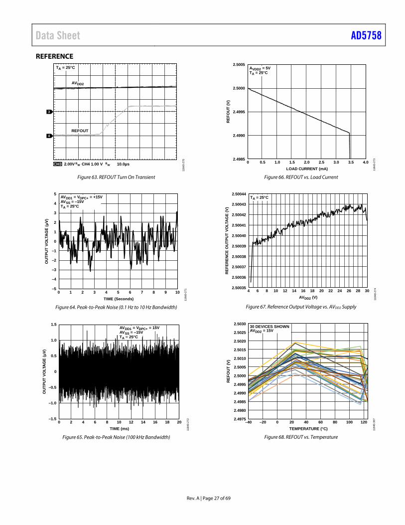
REFERENCE
10.0µs
3
4
BWCH3 2.00V CH4 1.00 VBW
1184
0-27
0
TA = 25°C
AVDD2
REFOUT
Figure 63. REFOUT Turn On Transient
5
4
3
2
1
0
–1
–2
–3
–4
–50 1 2 3 4 5 6 7 8 9 10
TIME (Seconds)
OUT
PUT
VOLT
AGE
(μV)
1184
0-27
1
AVDD1 = VDPC+ = +15VAVSS = –15VTA = 25°C
Figure 64. Peak-to-Peak Noise (0.1 Hz to 10 Hz Bandwidth)
–1.5
–1.0
–0.5
0
0.5
1.0
1.5
0 2 4 6 8 10 12 14 16 18 20
OUT
PUT
VOLT
AGE
(μV)
TIME (ms) 1184
0-27
2
AVDD1 = VDPC+ = 15VAVSS = –15VTA = 25°C
Figure 65. Peak-to-Peak Noise (100 kHz Bandwidth)
2.5005
2.5000
2.4995
2.4990
2.4985
REFO
UT (V
)
0 0.5 1.0 1.5 2.0 3.0 4.02.5 3.5LOAD CURRENT (mA) 11
840-
273
AVDD2 = 5VTA = 25°C
Figure 66. REFOUT vs. Load Current
2.50035
2.50036
2.50037
2.50038
2.50039
2.50040
2.50041
2.50042
2.50043
2.50044
4 6 8 10 12 14 16 18 20 22 24 26 28 30
REFE
RENC
E O
UTPU
T VO
LTAG
E (V
)
AVDD2 (V)
TA = 25°C
1 184
0-27
4
Figure 67. Reference Output Voltage vs. AVDD2 Supply
2.4975
2.4980
2.4985
2.4990
2.4995
2.5000
2.5005
2.5010
2.5015
2.5020
2.5025
2.5030
–40 –20 0 20 40 60 80 100 120
REFO
UT (V
)
TEMPERATURE (°C)
30 DEVICES SHOWNAVDD2 = 15V
1184
0-36
7
Figure 68. REFOUT vs. Temperature

AD5758 Data Sheet
Rev. A | Page 28 of 69
GENERAL
0
10
20
30
40
50
60
70
80
0 0.5 1.0 1.5 2.0 2.5 3.0 3.5
V LO
GIC
CUR
RENT
(µA)
VOLTAGE AT PIN (V) 1184
0-28
1
VLOGIC = 3.3VTA = 25°C
Figure 69. VLOGIC Current vs. Logic Input Voltage
–2.0
–1.5
–1.0
–0.5
0
0.5
1.0
1.5
2.0
0 5 10 15 20 25 30 35
CURR
ENT
(mA)
VOLTAGE (V) 1184
0-27
8
VOUT = 0VTA = 25°C
AIDD1
AISS
Figure 70. AIDD1/AISS Current vs. AVDD1/|AVSS| Supply
0
0.1
0.2
0.3
0.4
0.5
0.6
0.7
0.8
0.9
1.0
0 5 10 15 20 25 30 35
CURR
ENT
(mA)
VOLTAGE (V) 1184
0-27
9
AIDD1
IOUT = 0mATA = 25°C
Figure 71. AIDD1 Current vs AVDD1 Supply
9.90
9.95
10.00
10.05
10.10
10.15
–40 25 70 105 125
FREQ
UENC
Y (M
Hz)
TEMPERATURE (°C) 1184
0-28
2
AVDD2 = 5.5VTA = 25°C
Figure 72. Internal Oscillator Frequency vs. Temperature
0 5 10 15 20 25 30 35 40 45 50 55 60 65 7570
V LDO
(V)
1184
0-27
63.21
3.22
3.23
3.24
3.25
3.26
3.27
3.28
3.29
3.30
3.31
LOAD CURRENT (mA)
AVDD2 = 15VTA = 25°C
Figure 73. VLDO vs. Load Current

Data Sheet AD5758
Rev. A | Page 29 of 69
TERMINOLOGY Total Unadjusted Error (TUE) TUE is a measure of the output error taking all the various errors into account, namely INL error, offset error, gain error, and output drift over supplies, temperature, and time. TUE is expressed in % FSR.
Relative Accuracy or Integral Nonlinearity (INL) For the DAC, relative accuracy, or INL, is a measure of the maximum deviation, in LSBs or % FSR, from the best fit line passing through the DAC transfer function.
Differential Nonlinearity (DNL) DNL is the difference between the measured change and the ideal 1 LSB change between any two adjacent codes. A specified differential nonlinearity of ±1 LSB maximum ensures monotonicity. This DAC is guaranteed monotonic by design.
Monotonicity A DAC is monotonic if the output either increases or remains constant for increasing digital input code. The AD5758 is monotonic over its full operating temperature range.
Zero-Scale/Negative Full-Scale Error Zero-scale/negative full-scale error is the error in the DAC output voltage when 0x0000 (straight binary coding) is loaded to the DAC output register.
Zero-Scale Temperature Coefficient (TC) Zero-scale TC is a measure of the change in zero-scale error with a change in temperature. Zero-scale error TC is expressed in ppm FSR/°C.
Bipolar Zero Error Bipolar zero error is the deviation of the analog output from the ideal half-scale output of 0 V when the DAC output register is loaded with 0x8000 (straight binary coding).
Bipolar Zero Temperature Coefficient (TC) Bipolar zero TC is a measure of the change in the bipolar zero error with a change in temperature. It is expressed in ppm FSR/°C.
Offset Error Offset error is the deviation of the analog output from the ideal and is measured using ¼ scale and ¾ scale digital code measurements. It is expressed in % FSR.
Offset Error (TC) Offset error TC is a measure of the change in the offset error with a change in temperature. It is expressed in ppm FSR/°C.
Gain Error Gain error is a measure of the span error of the DAC. It is the deviation in slope of the DAC transfer characteristic from the ideal expressed in % FSR.
Gain Error Temperature Coefficient (TC) Gain error TC is a measure of the change in gain error with changes in temperature. Gain error TC is expressed in ppm FSR/°C.
Full-Scale Error Full-scale error is a measure of the output error when full-scale code is loaded to the DAC output register. Ideally, the output is full-scale − 1 LSB. Full-scale error is expressed in % FSR.
Headroom This is the difference between the voltage required at the output (programmed voltage in voltage output mode and programmed current × RLOAD in current output mode) and the voltage supplied by the positive supply rail, VDPC+. Headroom is relevant when the output is positive with respect to ground.
Footroom Footroom is the difference between the voltage required at the output (programmed voltage in voltage output mode and programmed current × RLOAD in current output mode) and the voltage supplied by the negative supply rail, AVSS. Footroom is relevant when the output is negative with respect to ground.
VOUT/−VSENSE Common-Mode Rejection Ratio (CMRR) VOUT/−VSENSE CMRR is the error in VOUT voltage due to changes in –VSENSE voltage.
Current Loop Compliance Voltage The maximum voltage at the VIOUT pin for which the output current is equal to the programmed value.
Voltage Reference TC Voltage reference TC is a measure of the change in the reference output voltage with a change in temperature. The reference TC is calculated using the box method, which defines the TC as the maximum change in the reference output over a given temperature range expressed in ppm/°C, as follows:
_ _ 6
_
10REF MAX REF MIN
REF NOM
V VTC
V TempRange −
= × ×
where: VREF_MAX is the maximum reference output measured over the total temperature range. VREF_MIN is the minimum reference output measured over the total temperature range. VREF_NOM is the nominal reference output voltage, 2.5 V. TempRange is the specified temperature range, −40°C to +115°C.
Line Regulation Line regulation is the change in reference output voltage due to a specified change in power supply voltage. It is expressed in ppm/V.
Load Regulation Load regulation is the change in reference output voltage due to a specified change in reference load current. It is expressed in ppm/mA.
AD5758 Data Sheet
Rev. A | Page 30 of 69
Dynamic Power Control (DPC) In this mode, the AD5758 circuitry senses the output voltage and dynamically regulates the supply voltage, VDPC+, to meet compliance requirements plus an optimized headroom voltage for the output buffer.
Programmable Power Control (PPC) In this mode, the VDPC+ voltage is user-programmable to a fixed level that needs to accommodate the maximum output load required.
Output Voltage Settling Time Output voltage settling time is the amount of time it takes for the output to settle to a specified level for a full-scale input change. This specification depends on the manner in which the DPC feature is configured (enabled, disabled, PPC mode enabled) and on the characteristics of the external dc-to-dc inductor and capacitor components used.
Slew Rate The slew rate of a device is a limitation in the rate of change of the output voltage. The output slewing speed of a voltage output DAC is usually limited by the slew rate of the amplifier used at its output. Slew rate is measured from 10% to 90% of the output signal and is expressed in V/µs.
Power-On Glitch Energy Power-on glitch energy is the impulse injected into the analog output when the AD5758 is powered on. It is specified as the area of the glitch in nV-sec.
Digital-to-Analog Glitch Energy Digital-to-analog glitch energy is the energy of the impulse injected into the analog output when the input code in the DAC output register changes state. It is normally specified as the area of the glitch in nV-sec. Worst case is usually when the digital input code is changed by 1 LSB at the major carry transition (0x7FFF to 0x8000).
Glitch Impulse Peak Amplitude Glitch impulse peak amplitude is the peak amplitude of the impulse injected into the analog output when the input code in the DAC output register changes state. It is specified as the amp-litude of the glitch in millivolts and the worst case is usually when the digital input code is changed by 1 LSB at the major carry transition (0x7FFF to 0x8000).
Digital Feedthrough Digital feedthrough is a measure of the impulse injected into the analog output of the DAC from the digital inputs of the DAC but is measured when the DAC output is not updated (LDAC pin is held high). It is specified in nV-sec and measured with a full-scale code change on the data bus.
Power Supply Rejection Ratio (PSRR) PSRR indicates how the output of the DAC is affected by changes in the power supply voltage.

Data Sheet AD5758
Rev. A | Page 31 of 69
THEORY OF OPERATION The AD5758 is a single-channel, precision voltage and current output DAC, designed to meet the requirements of industrial factory automation and process control applications. It provides a high precision, fully integrated, single-chip solution for generat-ing a unipolar/bipolar current or voltage output. Package power dissipation is minimized by incorporating on-chip DPC, which is achieved by regulating the supply voltage (VDPC+) to the VIOUT output driver from 4.95 V to 27 V using a buck dc-to-dc converter, optimized for minimum on-chip power dissipation. The AD5758 consists of a two die solution with the dc-to-dc converter circuitry and the VIOUT line protector located on the dc-to-dc die, and the remaining circuitry on the main die. Interdie communication is performed over an internal 3-wire interface.
DAC ARCHITECTURE The DAC core architecture of the AD5758 consists of a voltage mode R-2R ladder network. The voltage output of the DAC core is either converted to a current or voltage output at the VIOUT pin. Only one mode can be enabled at any one time. Both the voltage and current output stages are supplied by the VDPC+ power rail (internally generated from AVDD1) and the AVSS rail.
Current Output Mode
If current output mode is enabled, the voltage output from the DAC is converted to a current (see Figure 74), which is then mirrored to the supply rail so that the application only sees a current source output.
The current ranges available are 0 mA to 20 mA, 0 mA to 24 mA, 4 mA to 20 mA, ±20 mA, ±24 mA, and −1 mA to +22 mA. An internal or external 13.7 kΩ RSET resistor can be used for the voltage to current conversion.
RA
VIOUTRSET
Vx
VSS
VDPC+
R1 R4
R2 R3
RB
IOUTOPEN FAULT
16-BITDAC
1184
0-02
3
Figure 74. Voltage to Current Conversion Circuitry
Voltage Output Mode
If voltage output mode is enabled, the voltage output from the DAC is buffered and scaled to output a software-selectable unipolar or bipolar voltage range (see Figure 75).
The voltage ranges available are 0 V to 5 V, ±5 V, 0 V to 10 V, and ±10 V. A 20% overrange feature is also available via the DAC_ CONFIG register, as well as the facility to negatively offset the unipolar voltage ranges via the GP_CONFIG1 register (see the General-Purpose Configuration 1 Register section).
RANGESCALINGDAC
VOUT SHORT FAULT
+VSENSE
–VSENSE
VIOUT
1184
0-02
4
Figure 75. Voltage Output
Reference
The AD5758 can operate with either an external or internal reference. The reference input requires a 2.5 V reference for specified performance. This input voltage is then internally buffered before it is applied to the DAC.
The AD5758 contains an integrated buffered 2.5 V voltage reference that is externally available for use elsewhere within the system. The internal reference drives the integrated 12-bit ADC. REFOUT must be connected to REFIN to use the internal reference to drive the DAC.
SERIAL INTERFACE The AD5758 is controlled over a versatile 4-wire serial interface that operates at clock rates of up to 50 MHz and is compatible with SPI, QSPI, MICROWIRE, and DSP standards. Data coding is always straight binary.
Input Shift Register
With SPI CRC enabled (default state), the input shift register is 32 bits wide. Data is loaded into the device MSB first as a 32-bit word under the control of a serial clock input, SCLK. Data is clocked in on the falling edge of SCLK. If CRC is disabled, the serial interface is reduced to 24 bits; a 32-bit frame is still accepted but the last 8 bits are ignored. See the Register Map section for full details on the registers that can be addressed via the SPI interface.
Table 7. Writing to a Register (CRC enabled) MSB LSB D31 [D30:D29] [D28:D24] [D23:D8] [D7:D0] Slip Bit AD5758
address Register address
Data CRC

AD5758 Data Sheet
Rev. A | Page 32 of 69
Transfer Function
Table 8 shows the input code to ideal output voltage relationship for the AD5758 for straight binary data coding of the ±5 V output range.
Table 8. Ideal Output Voltage to Input Code Relationship
Digital Input, Straight Binary Data Coding
Analog Output
MSB LSB VOUT
1111 1111 1111 1111 +2 VREF × (32,767/32,768) 1111 1111 1111 1110 +2 VREF × (32,766/32,768) 1000 0000 0000 0000 0 V 0000 0000 0000 0001 −2 VREF × (32,767/32,768) 0000 0000 0000 0000 −2 VREF
POWER-ON STATE OF THE AD5758 On initial power-on or a device reset of the AD5758, the voltage and current output channels are disabled. The switch connecting VIOUT via a 30 kΩ pull-down resistor to AGND is open. This switch can be configured in the DCDC_CONFIG2 register. VDPC+ is internally driven to 4.8 V on power-on, until the dc-to-dc converter is enabled.
After device power-on, or a device reset, a calibration memory refresh command is required (see the Programming Sequence to Enable the Output section). It is recommended to wait 500 μs minimum after writing this command, before writing further instructions to the device to allow time for internal calibrations to take place (see Figure 90).
Power-On Reset
3.3VLDO
POWER-ONRESET
SOFTWARERESET
HARDWARERESET
INT_AVCC
RESET
SDISCLK
VLDO
AVDD2
SYNC
1184
0-12
5
Figure 76. Power-On Reset Block Diagram
The AD5758 incorporates a power-on reset circuit that ensures the AD5758 is held in reset while the power supplies are at a level insufficient to allow reliable operation. The power-on reset circuit (see Figure 76) monitors the AVDD2 generated VLDO and INT_AVCC voltages, the RESET pin, and the SPI reset signal. The power-on reset circuit keeps the AD5758 in reset until the voltages on the VLDO and INT_AVCC nodes are sufficient for reliable operation. If the power-on circuit receives a signal from the RESET pin, or if a software reset is written to the AD5758 via the SPI interface, the AD5758 is reset. Do not write SPI commands to the device within 100 μs of a reset event.
POWER SUPPLY CONSIDERATIONS The AD5758 has four supply rails: AVDD1, AVDD2, AVSS, and VLOGIC. See Table 1 for the voltage range of the four supply rails and the associated conditions.
AVDD1 Considerations
AVDD1 is the supply rail for the dc-to-dc converter and can range from 7 V to 33 V. Although the maximum value of AVDD1 is 33 V and the minimum value of AVSS is −33 V, the maximum operating range of |AVDD1 to AVSS| is 60 V. VDPC+ is derived from AVDD1, and its value depends on the mode of operation of the dc-to-dc converter.
The dc-to-dc converter requires a sufficient level of margin to be maintained between AVDD1 and VDPC+ to ensure the dc-to-dc circuitry operates correctly. This margin is 5% of the maximum VDPC+ voltage for a given mode of operation.
Table 9. AVDD1 to VDPC+ Margin Mode of Operation VDPC+ Maximum DPC Voltage Mode 15 V DPC Current Mode (IOUT maximum × RLOAD) + IOUT headroom PPC Current Mode DCDC_CONFIG1[4:0] programmed value
See the Power Dissipation Control section for further details on the dc-to-dc converter modes of operation.
Assuming DPC current mode, IOUT maximum = 20 mA; RLOAD = 1 kΩ IOUT headroom = 2.5 V VDPC+ maximum = 20 V + 2.5 V = 22.5 V
|VDPC+ to AVDD1| headroom can be calculated as 5% of 22.5 V = 1.125 V. Therefore, AVDD1 (minimum) = 22.5 V + 1.125 V = 23.625 V. Assuming a worst case AVDD1 supply rail tolerance of ±10%, this example requires an AVDD1 supply rail of approximately 26 V.
Data Sheet AD5758
Rev. A | Page 33 of 69
AVSS Considerations AVSS is the negative supply rail and has a range of −33 V to 0 V. As in the case of AVDD1, AVSS must obey the maximum operating range of |AVDD1 to AVSS| of 60 V. For bipolar current output ranges, the maximum AVSS can be calculated as (IOUT_MAX × RLOAD) + IOUT foot-room. For unipolar current output ranges, AVSS can be tied to AGND (that is, 0 V). For unipolar voltage output ranges, the maximum AVSS is −2 V to enable sufficient footroom for the internal voltage output circuitry. To avoid power supply sequencing issues, a Schottky diode must be placed between AVSS and GND (the GND supply must always be available).
AVDD2 Considerations
AVDD2 is the positive low voltage supply rail and has a range of 5 V to 33 V. If only one positive power rail is available, AVDD2 can be tied to AVDD1. However, to optimize for reduced power dissipation, supply AVDD2 with a separate lower voltage supply.
VLOGIC Considerations VLOGIC is the digital supply for the device and can range from 1.71 V to 5.5 V. The 3.3 V VLDO output voltage can be used to drive VLOGIC.
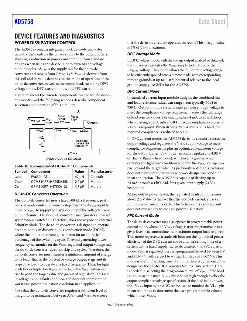
AD5758 Data Sheet
Rev. A | Page 34 of 69
DEVICE FEATURES AND DIAGNOSTICS POWER DISSIPATION CONTROL The AD5758 contains integrated buck dc-to-dc converter circuitry that controls the power supply to the output buffers, allowing a reduction in power consumption from standard designs when using the device in both current and voltage output modes. AVDD1 is the supply rail for the dc-to-dc converter and ranges from 7 V to 33 V. VDPC+ is derived from this rail and its value depends on the mode of operation of the dc-to-dc converter, as well as the output load, including DPC voltage mode, DPC current mode, and PPC current mode
Figure 77 shows the discrete components needed for the dc-to-dc circuitry and the following sections describe component selection and operation of this circuitry.
LDCDC CDCDC2.2µF47µHCIN
4.7µF0.1µF
AVDD1
DC-TO-DCCONVERTER CIRCUITRY
SW+ VDPC+ PGND1
VDPC+
PGND1
11840-021
Figure 77. DC-to-DC Circuit
Table 10. Recommended DC-to-DC Components Symbol Component Value Manufacturer LDCDC PA6594-AE 47 μH Coilcraft CDCDC GCM31CR71H225KA55L 2.2 μF Murata CIN GRM31CR71H475KA12L 4.7 μF Murata
DC-to-DC Converter Operation
The dc-to-dc converter uses a fixed 500 kHz frequency, peak current mode control scheme to step down the AVDD1 input to produce VDPC+ to supply the driver circuitry of the voltage/current output channel. The dc-to-dc converter incorporates a low-side synchronous switch and, therefore, does not require an external Schottky diode. The dc-to-dc converter is designed to operate predominantly in discontinuous conduction mode (DCM), where the inductor current goes to zero for an appreciable percentage of the switching cycle. To avoid generating lower frequency harmonics on the VDPC+ regulated output voltage rail, the dc-to-dc converter does not skip any cycles. Therefore, the dc-to-dc converter must transfer a minimum amount of energy to its load (that is, the current or voltage output stage and its respective load) to operate at a fixed frequency. Thus, for light loads (for example, low RLOAD or low IOUT), the VDPC+ voltage can rise beyond the target value and go out of regulation. This rise in voltage is not a fault condition and does not represent the worst case power dissipation condition in an application.
Note that the dc-to-dc converter requires a sufficient level of margin to be maintained between AVDD1 and VDPC+ to ensure
that the dc-to-dc circuitry operates correctly. This margin value is 5% of VDPC+ maximum.
DPC Voltage Mode
In DPC voltage mode, with the voltage output enabled or disabled, the converter regulates the VDPC+ supply to 15 V above the −VSENSE voltage. This mode allows the full output voltage range to be efficiently applied across remote loads, with corresponding remote grounds at up to ±10 V potential relative to the local ground supply (AGND) for the AD5758.
DPC Current Mode
In standard current input module designs, the combined line and load resistance values can range from typically 50 Ω to 750 Ω. Output module systems must provide enough voltage to meet the compliance voltage requirement across the full range of load resistor values. For example, in a 4 mA to 20 mA loop, when driving 20 mA into a 750 Ω load, a compliance voltage of >15 V is required. When driving 20 mA into a 50 Ω load, the required compliance is reduced to >1 V.
In DPC current mode, the AD5758 dc-to-dc circuitry senses the output voltage and regulates the VDPC+ supply voltage to meet compliance requirements plus an optimized headroom voltage for the output buffer. VDPC+ is dynamically regulated to 4.95 V or (IOUT × RLOAD + headroom), whichever is greater, which excludes the light load condition whereby the VDPC+ voltage can rise beyond the target value. As previously noted, this exclusion does not represent the worst case power dissipation condition in an application. The AD5758 is capable of driving up to 24 mA through a 1 kΩ load, for a given input supply (24 V + headroom).
At low output power levels, the regulated headroom increases above 2.3 V due to the fact that the dc-to-dc circuitry uses a minimum on time duty cycle. This behaviour is expected and does not impact any worse case power dissipation.
PPC Current Mode
The dc-to-dc converter may also operate in programmable power control mode, where the VDPC+ voltage is user-programmable to a given level to accommodate the maximum output load required. This mode represents a trade-off between the optimized power efficiency of the DPC current mode and the settling time of a system with a fixed supply (dc-to-dc disabled). In PPC current mode, VDPC+ is regulated to a user-programmable level between 5 V and 25.677 V with respect to −VSENSE (in steps of 0.667 V). This mode is useful if settling time is an important requirement of the design. See the DC-to-DC Converter Settling Time section. Care is needed in selecting the programmed level of VDPC+ if the load is nonlinear in nature. VDPC+ must be set high enough to obey the output compliance voltage specification. If the load is unknown, the +VSENSE input to the ADC can be used to monitor the VIOUT pin in current mode to determine the user-programmable value at which to set VDPC+.

Data Sheet AD5758
Rev. A | Page 35 of 69
DC-to-DC Converter Settling Time
When in DPC current mode, the settling time is dominated by the settling time of the dc-to-dc converter and is typically 200 µs without the digital slew rate control feature enabled. To reduce initial VIOUT waveform overshoot without adding a capacitor on VIOUT and thereby affecting HART operation, enable the digital slew rate control feature using the DAC_CONFIG register (see Table 32).
Table 11 shows the typical settling time for each of the dc-to-dc converter modes. All values shown assume the use of the components recommended by Analog Devices, Inc., listed in Table 10. The achievable settling time in any given application is dependent on the choice of external inductor and capacitor components used, as well as the current-limit setting of the dc-to-dc converter.
Table 11. Settling Time vs. DC-to-DC Converter Mode DC-to-DC Converter Mode Settling Time (µs) DPC Current Mode 200 PPC Current Mode 15 DPC Voltage Mode 15
DC-to-DC Converter Inductor Selection
For typical 4 mA to 20 mA applications, a 47 μH inductor (per Table 10), combined with the switching frequency of 500 kHz, allows up to 24 mA to be driven into a load resistance of up to 1 kΩ with an AVDD1 supply of greater than 24 V + headroom. It is important to ensure that the peak current does not cause the inductor to saturate, especially at the maximum ambient temperature. If the inductor enters saturation mode, it results in a decrease in efficiency. Larger size inductors translate to lower core losses. The slew rate control feature of the AD5758 can be used to limit peak currents during slewing. Program an appropriate current limit (via the DCDC_CONFIG2 register) to shut off the internal switch if the inductor current reaches that limit.
DC-to-DC Converter Input and Output Capacitor Selection The output capacitor, CDCDC, affects the ripple voltage of the dc-to-dc converter and limits the maximum slew rate at which the output current can rise. The ripple voltage is directly related to the output capacitance. The CDCDC capacitor recommended by Analog Devices (see Table 10), combined with the recommended 47 µH inductor, results in a 500 kHz ripple with amplitude less than 50 mV and guarantees stability and operation with HART capability across all operating modes.
For high voltage capacitors, the size of the capacitor is often an indication of the charge storage ability. It is important to characterize the dc bias voltage vs. capacitance curve for this capacitor. Any capacitance values specified are with reference to a dc bias corresponding to the maximum VDPC+ voltage in the application. As well as the voltage rating, the temperature range of the capacitor must also be considered for a given application. These considerations are key in selection of the components described in Table 10.
The input capacitor, CIN, provides much of the dynamic current required for the dc-to-dc converter, and a low effective series resistance (ESR) component is recommended. For the AD5758, a low ESR tantalum or ceramic capacitor of 4.7 μF (1206 size) in parallel with a 0.1 μF (0402 size) capacitor is recommended. Ceramic capacitors must be chosen carefully because they can exhibit a large sensitivity to dc bias voltages and temperature. X5R or X7R dielectrics are preferred because these capacitors remain stable over wider operating voltage and temperature ranges. Care must be taken if selecting a tantalum capacitor to ensure a low ESR value.
CLKOUT The AD5758 can provide a CLKOUT signal to the system for synchronization purposes. This signal is programmable to eight frequency options between 416 kHz and 588 kHz, with the default option being 500 kHz—the same switching frequency of the dc-to-dc converter. This feature is configured in the GP_CONFIG1 register and is disabled by default
INTERDIE 3-WIRE INTERFACE A 3-wire interface is used to communicate between the two die in the AD5758. The 3-wire interface master is located on the main die, and the 3-wire interface slave is on the dc-to-dc die. The three interface signals are data, DCLK (running at MCLK/8), and interrupt.
The main purpose of the 3-wire interface is to read from or write to the DCDC_CONFIG1 and DCDC_CONFIG2 registers. Addressing these registers via the SPI interface initiates an internal 3-wire interface transfer from the main die to the dc-to-dc die. The 3-wire interface master on the main die initiates writes and reads to the registers on the dc-to-dc die using DCLK as the serial clock. The slave uses an interrupt signal to the dc-to-dc die to indicate that a read of the dc-to-dc die internal status register is required.
For every 3-wire interface write, an automatic read and compare process can be enabled (default case) to ensure that the contents of the copy of the DCDC_CONFIGx registers on the main die match the contents of the registers on the dc-to-dc die. This comparison is performed to ensure the integrity of the digital circuitry on the dc-to-dc die. With this feature enabled, a 3-wire interface transfer takes approximately 300 µs. When disabled, this transfer time reduces to 30 µs.
The BUSY_3WI flag in the DCDC_CONFIG2 register is asserted during the 3-wire interface transaction. The BUSY_3WI flag is also set when the user updates the DAC range (via the DAC_ CONFIG register, Bits[4:0]) due to the internal calibration memory refresh caused by this action, which requires a 3-wire interface transfer between the two die. A write to either of the DCDC_CONFIGx registers must not be initiated while BUSY_3WI is asserted. If a write occurs while BUSY_3WI is asserted, the new write is delayed until the current 3-wire interface (3WI) transfer completes.

AD5758 Data Sheet
Rev. A | Page 36 of 69
3-Wire Interface Diagnostics
Any faults on the dc-to-dc die triggers an interrupt to the main die. An automatic status read of the dc-to-dc die is performed. After the read transaction, the main die retains a copy of the dc-to-dc die status bits (FAULT_PROT_SW_ERR, DCDC_P_SC_ERR, and DCDC_P_PWR_ERR). These values are available in the ANALOG_DIAG_RESULTS register and via the OR’d analog diagnostic results bits in the status register. These bits also trigger the FAULT pin.
In response to the interrupt request, the main die (master) performs a 3-wire interface read operation to read the status of the dc-to-dc die. The interrupt is only asserted again by a subsequent dc-to-dc die fault flag, upon which the 3-wire interface initiates another status read transaction. If an interrupt signal is detected six times in a row, the interrupt detection mechanism is disabled until a 3-wire interface write transaction completes. This disabling prevents the 3-wire interface from being blocked because of the constant dc-to-dc die status read when the interrupt is toggling. The INTR_SAT_3WI flag in the DCDC_CONFIG2 register indicates when this event occurs, and a write to either DCDC_CONFIGx register resets this bit to 0.
During a 3-wire read or write operation, the address and data bits in the transaction produce parity bits. These parity bits are checked on the receive side and, if they do not match on both die, the ERR_ 3WI bit in the DIGITAL_DIAG_RESULTS register is set. If the read and compare process is enabled and a parity error occurs, the 3WI_RC_ERR bit in the DIGITAL_DIAG_ RESULTS register is also set.
VOLTAGE OUTPUT Voltage Output Amplifier and VSENSE Functionality
The voltage output amplifier is capable of generating both unipolar and bipolar output voltages, and is also capable of driving a load of 1 kΩ in parallel with 2 μF (with an external compensation capacitor) to AGND. Figure 78 shows the voltage output driving a load, RLOAD, on top of a common-mode voltage (VCM) of ±10 V. An integrated 2 MΩ resistor ensures that the amplifier loop is kept closed, thus preventing potential large destructive voltages on VIOUT due to the broken amplifier loop in applications where a cable may become disconnected from +VSENSE. If remote sensing of the load is not required, connect +VSENSE directly to VIOUT and connect −VSENSE directly to AGND.
AD5758
VOUTRANGESCALING
16-BITADC
2MΩ
+VSENSE
+VSENSE RLOAD
VIOUT
2MΩ±10V VCM
11840-121
Figure 78. Voltage Output
Driving Large Capacitive Loads
The voltage output amplifier is capable of driving capacitive loads of up to 2 μF with the addition of a 220 pF nonpolarized compensation capacitor. This capacitor, while allowing the AD5758 to drive higher capacitive loads and reduce overshoot, increases the settling time of the device and, therefore, affects the bandwidth of the system. Without the compensation capacitor, capacitive loads of up to 10 nF can be driven.
Voltage Output Short-Circuit Protection
Under normal operation, the voltage output sinks/sources up to 12 mA and maintains specified operation. The short-circuit current is typically 16 mA. If a short circuit is detected, the FAULT pin goes low and the VOUT_SC_ERR bit in the ANALOG_DIAG_RESULTS register is set.
FAULT PROTECTION The AD5758 incorporates a line protector on the VIOUT pin, +VSENSE pin, and −VSENSE pin. The line protector operates by clamping the voltage internal to the line protector to the VDPC+ and AVSS rails, thereby protecting internal circuitry from external voltage faults. If a voltage outside of these limits is detected on the VIOUT pin, an error flag (VIOUT_OV_ERR) is also set and is located in the ANALOG_DIAG_RESULTS register.
CURRENT OUTPUT External Current Setting Resistor
As shown in Figure 74, RSET is an internal sense resistor that forms part of the voltage to current conversion circuitry. The stability of the output current value over temperature is dependent on the stability of the value of RSET. As a method of improving the stability of the output current over temperature, an external, 13.7 kΩ, low drift resistor can be connected between the RA and RB pins of the AD5758, to be used instead of the internal resistor.
Table 1 shows the performance specifications of the AD5758 with both the internal RSET resistor and an external, 13.7 kΩ RSET resistor. The external RSET resistor specification assumes an ideal resistor. The actual performance depends on the absolute value and temperature coefficient of the resistor used. Therefore, the resistor specifications directly affect the gain error of the output and the TUE.
To arrive at the absolute worst case overall TUE of the output with a particular external RSET resistor, add the percentage absolute error of the RSET resistor directly to the TUE of the AD5758 with the external RSET resistor, shown in Table 1 (expressed in % FSR). The temperature coefficient must also be considered, as well as the specifications of the external reference, if this is the option being used in the system.
The magnitude of the error derived from directly summing the absolute error and TC error of both the external RSET resistor and the external reference with the TUE specification of the AD5758 is unlikely to occur because the TC values of the individual components are not likely to exhibit the same drift polarity, and, therefore, an element of cancelation occurs. For
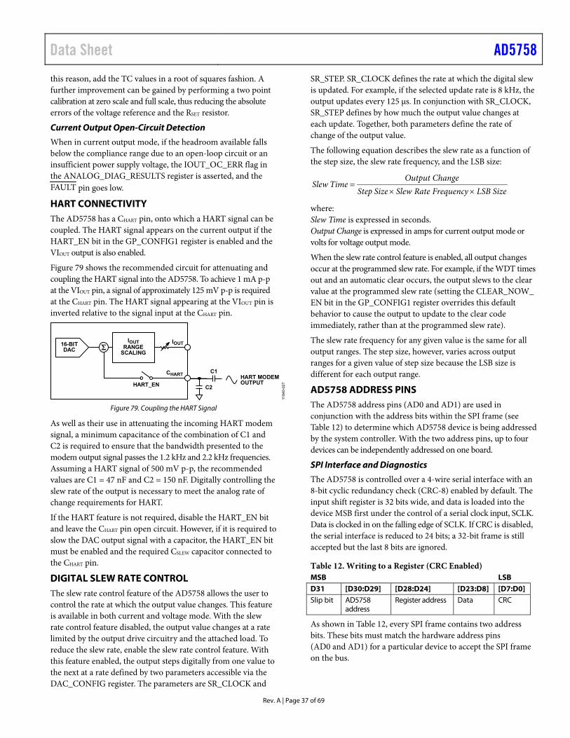
Data Sheet AD5758
Rev. A | Page 37 of 69
this reason, add the TC values in a root of squares fashion. A further improvement can be gained by performing a two point calibration at zero scale and full scale, thus reducing the absolute errors of the voltage reference and the RSET resistor.
Current Output Open-Circuit Detection
When in current output mode, if the headroom available falls below the compliance range due to an open-loop circuit or an insufficient power supply voltage, the IOUT_OC_ERR flag in the ANALOG_DIAG_RESULTS register is asserted, and the FAULT pin goes low.
HART CONNECTIVITY The AD5758 has a CHART pin, onto which a HART signal can be coupled. The HART signal appears on the current output if the HART_EN bit in the GP_CONFIG1 register is enabled and the VIOUT output is also enabled.
Figure 79 shows the recommended circuit for attenuating and coupling the HART signal into the AD5758. To achieve 1 mA p-p at the VIOUT pin, a signal of approximately 125 mV p-p is required at the CHART pin. The HART signal appearing at the VIOUT pin is inverted relative to the signal input at the CHART pin.
HART MODEMOUTPUT
C1
C2
11840-027
16-BITDAC
IOUT
CHART
IOUTRANGE
SCALING
HART_EN
Figure 79. Coupling the HART Signal
As well as their use in attenuating the incoming HART modem signal, a minimum capacitance of the combination of C1 and C2 is required to ensure that the bandwidth presented to the modem output signal passes the 1.2 kHz and 2.2 kHz frequencies. Assuming a HART signal of 500 mV p-p, the recommended values are C1 = 47 nF and C2 = 150 nF. Digitally controlling the slew rate of the output is necessary to meet the analog rate of change requirements for HART.
If the HART feature is not required, disable the HART_EN bit and leave the CHART pin open circuit. However, if it is required to slow the DAC output signal with a capacitor, the HART_EN bit must be enabled and the required CSLEW capacitor connected to the CHART pin.
DIGITAL SLEW RATE CONTROL The slew rate control feature of the AD5758 allows the user to control the rate at which the output value changes. This feature is available in both current and voltage mode. With the slew rate control feature disabled, the output value changes at a rate limited by the output drive circuitry and the attached load. To reduce the slew rate, enable the slew rate control feature. With this feature enabled, the output steps digitally from one value to the next at a rate defined by two parameters accessible via the DAC_CONFIG register. The parameters are SR_CLOCK and
SR_STEP. SR_CLOCK defines the rate at which the digital slew is updated. For example, if the selected update rate is 8 kHz, the output updates every 125 μs. In conjunction with SR_CLOCK, SR_STEP defines by how much the output value changes at each update. Together, both parameters define the rate of change of the output value.
The following equation describes the slew rate as a function of the step size, the slew rate frequency, and the LSB size:
Output ChangeSlew Time
Step Size Slew Rate Frequency LSB Size
where: Slew Time is expressed in seconds. Output Change is expressed in amps for current output mode or volts for voltage output mode.
When the slew rate control feature is enabled, all output changes occur at the programmed slew rate. For example, if the WDT times out and an automatic clear occurs, the output slews to the clear value at the programmed slew rate (setting the CLEAR_NOW_ EN bit in the GP_CONFIG1 register overrides this default behavior to cause the output to update to the clear code immediately, rather than at the programmed slew rate).
The slew rate frequency for any given value is the same for all output ranges. The step size, however, varies across output ranges for a given value of step size because the LSB size is different for each output range.
AD5758 ADDRESS PINS The AD5758 address pins (AD0 and AD1) are used in conjunction with the address bits within the SPI frame (see Table 12) to determine which AD5758 device is being addressed by the system controller. With the two address pins, up to four devices can be independently addressed on one board.
SPI Interface and Diagnostics
The AD5758 is controlled over a 4-wire serial interface with an 8-bit cyclic redundancy check (CRC-8) enabled by default. The input shift register is 32 bits wide, and data is loaded into the device MSB first under the control of a serial clock input, SCLK. Data is clocked in on the falling edge of SCLK. If CRC is disabled, the serial interface is reduced to 24 bits; a 32-bit frame is still accepted but the last 8 bits are ignored.
Table 12. Writing to a Register (CRC Enabled) MSB LSB
D31 [D30:D29] [D28:D24] [D23:D8] [D7:D0] Slip bit AD5758
address Register address Data CRC
As shown in Table 12, every SPI frame contains two address bits. These bits must match the hardware address pins (AD0 and AD1) for a particular device to accept the SPI frame on the bus.
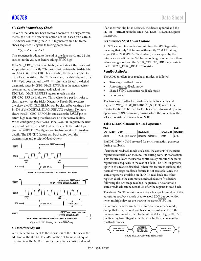
AD5758 Data Sheet
Rev. A | Page 38 of 69
SPI Cyclic Redundancy Check
To verify that data has been received correctly in noisy environ-ments, the AD5758 offers the option of CRC based on a CRC-8. The device controlling the AD5758 generates an 8-bit frame check sequence using the following polynomial:
C(x) = x8 + x2 + x1 + 1
This sequence is added to the end of the data-word, and 32 bits are sent to the AD5758 before taking SYNC high.
If the SPI_CRC_EN bit is set high (default state), the user must supply a frame of exactly 32 bits wide that contains the 24 data bits and 8-bit CRC. If the CRC check is valid, the data is written to the selected register. If the CRC check fails, the data is ignored, the FAULT pin goes low and the FAULT pin status bit and the digital diagnostic status bit (DIG_DIAG_STATUS) in the status register are asserted. A subsequent readback of the DIGITAL_DIAG_RESULTS register reveals that the SPI_CRC_ERR bit is also set. This register is a per bit, write to clear register (see the Sticky Diagnostic Results Bits section); therefore, the SPI_CRC_ERR bit can be cleared by writing a 1 to Bit D0 of the DIGITAL_DIAG_RESULTS register. Doing so clears the SPI_CRC_ERROR bit and causes the FAULT pin to return high (assuming that there are no other active faults). When configuring the FAULT_PIN_CONFIG register, the user can decide whether the SPI CRC error affects the FAULT pin. See the FAULT Pin Configuration Register section for further details. The SPI CRC feature can be used for both the transmission and receipt of data packets.
SDI
SYNC
SCLK
UPDATE ON SYNC HIGH
MSBD23
LSBD0
24-BIT DATA
24-BIT DATA TRANSFER—NO CRC ERROR CHECKING
SDI
FAULT
SYNC
SCLK
UPDATE ON SYNC HIGHONLY IF CRC CHECK PASSED
FAULT PIN GOES LOWIF CRC CHECK FAILS
MSBD31
LSBD8 D7 D0
24-BIT DATA 8-BIT CRC
32-BIT DATA TRANSFER WITH CRC ERROR CHECKING 1184
0-02
5
Figure 80. CRC Timing (Assume LDAC = 0)
SPI Interface Slip Bit
A further enhancement to the robustness of the interface is the addition of the slip bit. The MSB of the SPI frame must equal the inverse of the MSB − 1 for the frame to be considered valid.
If an incorrect slip bit is detected, the data is ignored and the SLIPBIT_ERROR bit in the DIGITAL_DIAG_RESULTS register is asserted.
SPI Interface SCLK Count Feature
An SCLK count feature is also built into the SPI diagnostics, meaning that only SPI frames with exactly 32 SCLK falling edges (32 or 24 if SPI CRC is disabled) are accepted by the interface as a valid write. SPI frames of lengths other than these values are ignored and the SCLK_COUNT_ERR flag asserts in the DIGITAL_DIAG_RESULTS register.
Readback Modes
The AD5758 offers four readback modes, as follows:
Two stage readback mode Autostatus readback mode Shared SYNC autostatus readback mode Echo mode
The two stage readback consists of a write to a dedicated register, TWO_STAGE_READBACK_SELECT, to select the register location to be read back. This write is followed by a no operation (NOP) command, during which the contents of the selected register are available on SDO.
Table 13. SDO Contents for Read Operation MSB LSB
[D31:D30] D29 [D28:24] [D23:D8] [D7:D0]0b10 FAULT pin status Register address Data CRC
Bits[D31:D30] = 0b10 are used for synchronization purposes during readback.
If autostatus readback mode is selected, the contents of the status register are available on the SDO line during every SPI transaction. This feature allows the user to continuously monitor the status register and act quickly in the case of a fault. The AD5758 powers up with this feature disabled. When this feature is enabled, the normal two stage readback feature is not available. Only the status register is available on SDO. To read back any other register, disable the automatic readback feature first before following the two stage readback sequence. The automatic status readback can be reenabled after the register is read back.
The shared SYNC autostatus readback is a special version of the autostatus readback mode used to avoid SDO bus contention when multiple devices are sharing the same SYNC line.
Echo mode behaves similarly to autostatus readback mode, except that every second readback consists of an echo of the previous command written to the AD5758 (see Figure 81). See the Reading from Registers section for further details on the readback modes.
PREVIOUSCOMMAND
STATUSREGISTERCONTENTS
PREVIOUSCOMMAND
1184
0-01
9
Figure 81. SDO Contents, Echo Mode

Data Sheet AD5758
Rev. A | Page 39 of 69
WATCHDOG TIMER (WDT) The WDT feature is useful to ensure that communication is not lost between the system controller and the AD5758 and that the SPI datapath lines function as expected.
When enabled, the WDT alerts the system if the AD5758 has not received a specific SPI frame in the user-programmable timeout period. When the specific SPI frame is received, the watchdog resets the timer controlling the timeout alert. The SPI frame used to reset the WDT is configurable as one of the two following choices:
• A specific key code write to the key register (default). • A valid SPI write to any register.
When a watchdog timeout event occurs, there are two user configurable actions the AD5758 can take. The first user configurable action is to load the DAC output with a user defined clear code stored in the CLEAR_CODE register. The second user configurable action is to perform a software reset. These actions can be enabled via Bit 10 and Bit 9, respectively, in the WDT_CONFIG register. On a watchdog timeout event (regardless of Bit 10 or Bit 9 being enabled), a dedicated WDT_STATUS bit in the status register, as well as a WDT_ERR bit in the DIGITAL_DIAG_RESULTS register, alerts the user that the WDT timed out. Note that, after a WDT timeout occurs, all writes to the DAC_INPUT register, as well as the hardware or software LDAC events, are ignored until the active WDT fault flag within the DIGITAL_DIAG_RESULTS register clears.
After this flag clears, the WDT can be restarted by performing a subsequent WDT reset command.
On power-up, the WDT is disabled by default. The default timeout setting is 1 sec. The default method to reset the WDT is to write one specific key and, on timeout, the default action is to set the relevant flag bits and the FAULT pin. See Table 39 for the specific register bit details to support the configurability of the WDT operation.
USER DIGITAL OFFSET AND GAIN CONTROL The AD5758 has a USER_GAIN register and a USER_OFFSET register that allow trimming of the gain and offset errors from the entire signal chain. The 16-bit USER_GAIN register allows the user to adjust the gain of the DAC channel in steps of 1 LSB. The USER_GAIN register coding is straight binary, as shown in Table 14. The default code in the USER_GAIN register is 0xFFFF, which results in no gain factor applied to the programmed output. In theory, the gain can be tuned across the full range of the output. In practice, the maximum recommended gain trim is approximately 50% of the programmed range to maintain accuracy.
Table 14. Gain Register Adjustment Gain Adjustment Factor D15 D14 to D1 D0 1 1 1 1 65,535/65,536 1 1 0 … … … … 2/65,536 0 0 1 1/65,536 0 0 0
The 16-bit USER_OFFSET register allows the user to adjust the offset of the DAC channel by −32,768 LSBs to +32,768 LSBs in steps of 1 LSB. The USER_OFFSET register coding is straight binary, as shown in Table 15. The default code in the USER_ OFFSET register is 0x8000, which results in zero offset programmed to the output.
Table 15. Offset Register Adjustment Gain Adjustment D15 D13 to D2 D0 +32,768 LSBs 1 1 1 +32,767 LSBs 1 1 0 … … … … No Adjustment (Default) 1 0 0 … … … … −32,767 LSBs 0 0 1 −32,768 LSBs 0 0 0
The value (in decimal) that is written to the internal DAC register can be calculated by
1516 2
2)1(
_ −++
×= CM
DCodeDAC (1)
where: D is the code loaded to the DAC_INPUT register. M is the code in the USER_GAIN register (default code = 216 − 1). C is the code in the USER_OFFSET register (default code = 215).
Data from the DAC_INPUT register is processed by a digital multiplier and adder, controlled by the contents of the user gain and USER_OFFSET registers, respectively. The calibrated DAC data is then loaded to the DAC, dependent on the state of the LDAC pin.
Each time data is written to the USER_GAIN or USER_ OFFSET register, the DAC output is not automatically updated. Instead, the next write to the DAC_INPUT register uses these user gain and user offset values to perform a new calibration and automatically updates the channel. The read only DAC_ OUTPUT register represents the value currently available at the DAC output, except in the case of user gain and user offset calibration. In this case, the DAC_OUTPUT register represents the DAC data input by the user, on which the calibration is performed and not the result of the calibration.
Both the USER_GAIN register and the USER_OFFSET register have 16 bits of resolution. The correct method to calibrate the gain and offset is to first calibrate the gain and then calibrate the offset.

AD5758 Data Sheet
Rev. A | Page 40 of 69
DAC OUTPUT UPDATE AND DATA INTEGRITY DIAGNOSTICS Figure 82 shows a simplified version of the DAC input loading circuitry. If used, the USER_GAIN and USER_OFFSET registers must be updated before writing to the DAC_INPUT register.
VIOUT
INTERFACE LOGIC
OUTPUTAMPLIFIER
SDOSDI
16-BITDAC
REFIN
SYNC
LDAC(HARDWARE OR SOFTWARE)
DAC INPUTREGISTER
USERGAIN AND OFFSET
CALIBRATION
SCLK
DAC OUTPUTREGISTER
(READ ONLY)
CLEAR CODEREGISTER
CLEAR EVENT(WDT TIMEOUT)
1184
0-02
6
Figure 82. Simplified Serial Interface of Input Loading Circuitry
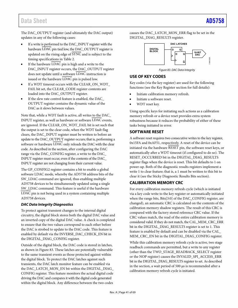
Data Sheet AD5758
Rev. A | Page 41 of 69
The DAC_OUTPUT register (and ultimately the DAC output) updates in any of the following cases:
If a write is performed to the DAC_INPUT register with the hardware LDAC pin tied low, the DAC_OUTPUT register is updated on the rising edge of SYNC and is subject to the timing specifications in Table 2.
If the hardware LDAC pin is high and a write to the DAC_INPUT register occurs, the DAC_OUTPUT register does not update until a software LDAC instruction is issued or the hardware LDAC pin is pulsed low.
If a WDT timeout occurs with the CLEAR_ON_WDT_ FAIL bit set, the CLEAR_CODE register contents are loaded into the DAC_OUTPUT register.
If the slew rate control feature is enabled, the DAC_ OUTPUT register contains the dynamic value of the DAC as it slews between values.
Note that, while a WDT fault is active, all writes to the DAC_ INPUT register, as well as hardware or software LDAC events, are ignored. If the CLEAR_ON_WDT_FAIL bit is set such that the output is set to the clear code, when the WDT fault flag clears, the DAC_INPUT register must be written to before an update to the DAC_OUTPUT register occurs; that is, performing a software or hardware LDAC only reloads the DAC with the clear code. As described in the section, after configuring the DAC range via the DAC_CONFIG register, a write to the DAC_ INPUT register must occur, even if the contents of the DAC_ INPUT register are not changing from their current value.
The GP_CONFIG2 register contains a bit to enable a global software LDAC mode, whereby the AD5758 address bits of the SW_LDAC command are ignored, thus enabling multiple AD5758 devices to be simultaneously updated using a single SW_LDAC command. This feature is useful if the hardware LDAC pin is not being used in a system containing multiple AD5758 devices.
DAC Data Integrity Diagnostics
To protect against transient changes to the internal digital circuitry, the digital block stores both the digital DAC value and an inverted copy of the digital DAC value. A check is completed to ensure that the two values correspond to each other before the DAC is strobed to update to the DAC code. This feature is enabled by default via the INVERSE_DAC_CHECK_EN bit in the DIGITAL_DIAG_CONFIG register.
Outside of the digital block, the DAC code is stored in latches, as shown in Figure 83. These latches are potentially vulnerable to the same transient events as those protected against within the digital block. To protect the DAC latches against such transients, the DAC latch monitor feature can be enabled via the DAC_LATCH_MON_EN bit within the DIGITAL_DIAG_ CONFIG register. This feature monitors the actual digital code driving the DAC and compares it with the digital code generated within the digital block. Any difference between the two codes
causes the DAC_LATCH_MON_ERR flag to be set in the DIGITAL_DIAG_RESULTS register.
16-BITDAC
DIGITALBLOCK D Q
QD Q
Q
DAC LATCHES
1184
0-02
8
Figure 83. DAC Data Integrity
USE OF KEY CODES Key codes (via the key register) are used for the following functions (see the Key Register section for full details):
Initiate calibration memory refresh. Initiate a software reset. WDT reset key.
Using specific keys for initiating such actions as a calibration memory refresh or a device reset provides extra system robustness because it reduces the probability of either of these tasks being initiated in error.
SOFTWARE RESET A software reset requires two consecutive writes to the key register, 0x15FA and 0xAF51, respectively. A reset of the device can be initiated via the hardware RESET pin, the software reset keys, or automatically after a WDT timeout (if configured to do so). The RESET_OCCURRED bit in the DIGITAL_DIAG_RESULTS register flags when the device is reset. This bit defaults to 1 on power-up. Both of the diagnostic results registers implement a write 1 to clear feature; that is, a 1 must be written to this bit to clear it (see the Sticky Diagnostic Results Bits section).
CALIBRATION MEMORY CRC For every calibration memory refresh cycle (which is initiated via a key code write to the key register or automatically initiated when the range bits, Bits[3:0] of the DAC_CONFIG register, are changed), an automatic CRC is calculated on the contents of the calibration memory shadow registers. The result of this CRC is compared with the factory stored reference CRC value. If the CRC values match, the read of the entire calibration memory is considered valid. If they do not match, the CAL_MEM_CRC_ERR bit in the DIGITAL_DIAG_RESULTS register is set to 1. This feature is enabled by default and can be disabled via the CAL_ MEM_CRC_EN bit in the DIGITAL_DIAG_CONFIG register.
While this calibration memory refresh cycle is active, two stage readback commands are permitted, but a write to any register (other than the TWO_STAGE_READBACK_SELECT register or the NOP register) causes the INVALID_SPI_ACCESS_ERR bit in the DIGITAL_DIAG_RESULTS register to set. As described in the section, a wait period of 500 μs is recommended after a calibration memory refresh cycle is initiated.

AD5758 Data Sheet
Rev. A | Page 42 of 69
INTERNAL OSCILLATOR DIAGNOSTICS An internal frequency monitor uses the internal oscillator (MCLK) to increment a 16-bit counter at a rate of 1 kHz (MCLK/10,000). The value of the counter is available to be read in the FREQ_ MONITOR register. The user can poll this register periodically and use it both as a diagnostic tool for the internal oscillator (to monitor that the oscillator is running), and to measure the frequency. This feature is enabled by default via the FREQ_MON_ EN bit in the DIGITAL_DIAG_CONFIG register.
In the event that the internal MCLK oscillator stops, the AD5758 sends a specific code of 0x07DEAD to the SDO line for every SPI frame. This feature is enabled by default and can be disabled by clearing the OSC_STOP_DETECT_EN bit in the GP_CONFIG1 register. Note that this feature is limited to the maximum readback timing specifications as outlined in Table 3.
STICKY DIAGNOSTIC RESULTS BITS The AD5758 contains two diagnostic results registers: digital and analog (see Table 44 and Table 45, respectively). The diagnostic result bits contained within these registers are sticky (R/W-1-C), that is, each bit needs a 1 to be written to it to clear it. A more appropriate word here is update rather than clear because if the fault is still present, even after writing a 1 to the bit in question, it does not clear to 0. Upon writing Logic 1 to the bit, it updates to its latest value, which is Logic 1 if the fault is still present and Logic 0 if the fault is no longer present.
There are two exceptions to this R/W-1-C access within the DIGITAL_DIAG_RESULTS register: CAL_MEMORY_ UNREFRESHED and SLEW_BUSY. These flags automatically clear when the calibration memory refresh or output slew, respectively, is complete.
The status register contains a DIG_DIAG_STATUS and ANA_DIAG_STATUS bit, which is the result of a logical OR of the diagnostic results bits contained in each of the diagnostic results registers. All analog diagnostic flag bits are included in the logical OR of the ANA_DIAG_STATUS bit and all digital diagnostic flag bits, with the exception of the SLEW_BUSY bit, are included in the logical OR of the DIG_DIAG_STATUS bit. The OR’d bits within the status register are read only and not sticky (R/W-1-C).
BACKGROUND SUPPLY AND TEMPERATURE MONITORING Excessive die temperature and overvoltage are known to be related to common cause failures. These conditions can be monitored in a continuous fashion using comparators, eliminating the requirement to poll the ADC.
Both die have a built-in temperature sensor with an accuracy of typically ±5oC. The die temperature is monitored by a comparator. The background temperature comparator is permanently enabled. Programmable trip points corresponding to 142°C, 127°C, 112°C, and 97°C can be configured in the GP_CONFIG1 register. If the temperature of the either die exceeds
the programmed limit, the relevant status bit in the ANALOG_ DIAG_RESULTS register is set and the FAULT pin is asserted low.
The low voltage supplies on the AD5758 are monitored via low power static comparators. This function is disabled by default and can be enabled via the COMPARATOR_CONFIG bits in the GP_CONFIG2 register. Note that the INT_EN bit in the DAC_CONFIG register must be set for the REFIN buffer to be powered up and for this node to be available to the REFIN comparator. The monitored nodes are REFIN, REFOUT, VLDO, and an internal AVCC voltage node (INT_AVCC). There is a status bit in the ANALOG_DIAG_RESULTS register corresponding to each monitored node. If any of the supplies exceed the upper or lower threshold values (see Table 16), the corresponding status bit is set. Note that, in the case of a REFOUT fault, the REFOUT_ERR status bit is set. In this case, the INT_AVCC, VLDO, and temperature comparator status bits may also become set because REFOUT is used as the comparison voltage for these nodes. Like all the other status bits in the ANALOG_ DIAG_RESULTS register, these bits are sticky and need a 1 to be written to them to clear them, assuming that the error condition subsided. If the error condition is still present, the flag remains high, even after a 1 is written to clear it.
Table 16. Comparator Supply Activation Thresholds
Supply Lower Threshold (V)
Nominal Value/Range (V)
Upper Threshold (V)
INT_AVCC 3.8 4 to 5 5.2 VLDO 2.8 3 to 3.6 3.8 REFIN 2.24 2.5 2.83 REFOUT 2.24 2.5 2.83
OUTPUT FAULT
The AD5758 is equipped with a FAULT pin. This pin is an active low, open-drain output allowing several AD5758 devices to be connected together to one pull-up resistor for global fault detection. This pin is high impedance when no faults are detected and is asserted low when certain faults are detected, for example, an open circuit in current mode, a short circuit in voltage mode, a CRC error, or an overtemperature error. Table 17 shows the fault conditions that automatically force the FAULT pin active and highlights the user maskable fault bits available via the FAULT_PIN_CONFIG register (see Table 42). Note that all registers contain a corresponding FAULT pin status bit, FAULT_PIN_STATUS, that mirrors the inverted current state of the FAULT pin. For example, if the FAULT pin is active, the FAULT_PIN_STATUS bit is 1.

Data Sheet AD5758
Rev. A | Page 43 of 69
Table 17. FAULT Pin Trigger Sources1
Fault Type Mapped to FAULT Pin
Mask Ability
Digital Diagnostic Faults Oscillator Stop Detect Yes Yes Calibration Memory Not Refreshed No N/A Reset Detected No N/A 3-Wire Interface Error Yes No WDT Error Yes Yes 3-Wire Read and Compare Parity Error Yes No DAC Latch Monitor Error Yes Yes Inverse DAC Check Error Yes Yes Calibration Memory CRC Error Yes No Invalid SPI Access Yes Yes SCLK Count Error Yes No2 Slip Bit Error Yes Yes SPI CRC Error Yes Yes
Analog Diagnostic Faults VIOUT Overvoltage Error Yes Yes DC-to-DC Short Circuit Error Yes Yes DC-to-DC Power Error Yes No Current Output Open Circuit Error Yes Yes Voltage Output Short-Circuit Error Yes Yes DC-to-DC Die Temperature Error Yes Yes Main Die Temperature Error Yes Yes REFFOUT Comparator Error Yes No REFIN Comparator Error Yes No INT_AVCC Comparator Error Yes No VLDO Comparator Error Yes No
1 N/A means not applicable. 2 Although the SCLK count error cannot be masked in the FAULT_PIN_CONFIG
register, it can be excluded from the FAULT pin by enabling the SPI_DIAG_ QUIET_EN bit (Bit D3 in the GP_CONFIG1 register).
The DIG_DIAG_STATUS, ANA_DIAG_STATUS, and WDT_ STATUS bits of the status register are used in conjunction with the FAULT pin and the FAULT_PIN_STATUS bit to inform the user which one of the fault conditions caused the FAULT pin or the FAULT_PIN_STATUS bit to be activated.
ADC MONITORING The AD5758 incorporates a 12-bit ADC to provide diagnostic information on user-selectable inputs, such as supplies, grounds, internal die temperatures, references, and external signals. See Table 18 for a full list of the selectable inputs. The reference used for the ADC is derived from REFOUT, providing a means of independence from the DAC reference (REFIN), if necessary. The ADC_CONFIG register configures the selection of the multiplexed ADC input channel via the ADC_IP_SELECT bits (see Table 41).
ADC Transfer Function Equations
The ADC has an input range of 0 V to 2.5 V and can be used to digitize a variety of different nodes. The set of inputs to the ADC encompasses both unipolar and bipolar ranges, varying from high to low voltage values. Therefore, to be able to digitize them, the voltage ranges outside of the 0 V to 2.5 V ADC input range must be divided down. The ADC transfer function equation is dependent on the selected ADC input node (see Table 18 for a summary of all transfer function equations).
Table 18. ADC Input Node Summary ADC_IP_SELECT VIN Node Description ADC Transfer Function 00000 Main die temperature T (°C) = (−0.09369 × D) + 307 00001 DC-to-dc die temperature T (°C) = (−0.11944 × D) + 436 00010 Reserved Reserved 00011 REFIN REFIN (V) = (D/212) × 2.75 00100 Internal 1.23 V reference voltage (REF2) REF2 (V) = (D/212) × 2.5 00101 Reserved Reserved 00110 Reserved Reserved 01100 Reserved Reserved 01101 Voltage on the +VSENSE buffer output +VSENSE (V) = ((50 × D)/212) − 25 01110 Voltage on the −VSENSE buffer output −VSENSE (V) = ((50 × D)/212) − 25 10000 Reserved Reserved 10001 Reserved Reserved 10010 Reserved Reserved 10011 Reserved Reserved 10100 INT_AVCC INT_AVCC (V) = D/212 × 10 10101 VLDO VLDO (V) = D/212 × 10 10110 VLOGIC VLOGIC (V) = D/212 × 10 11000 REFGND REFGND (V) = D/212 × 2.5
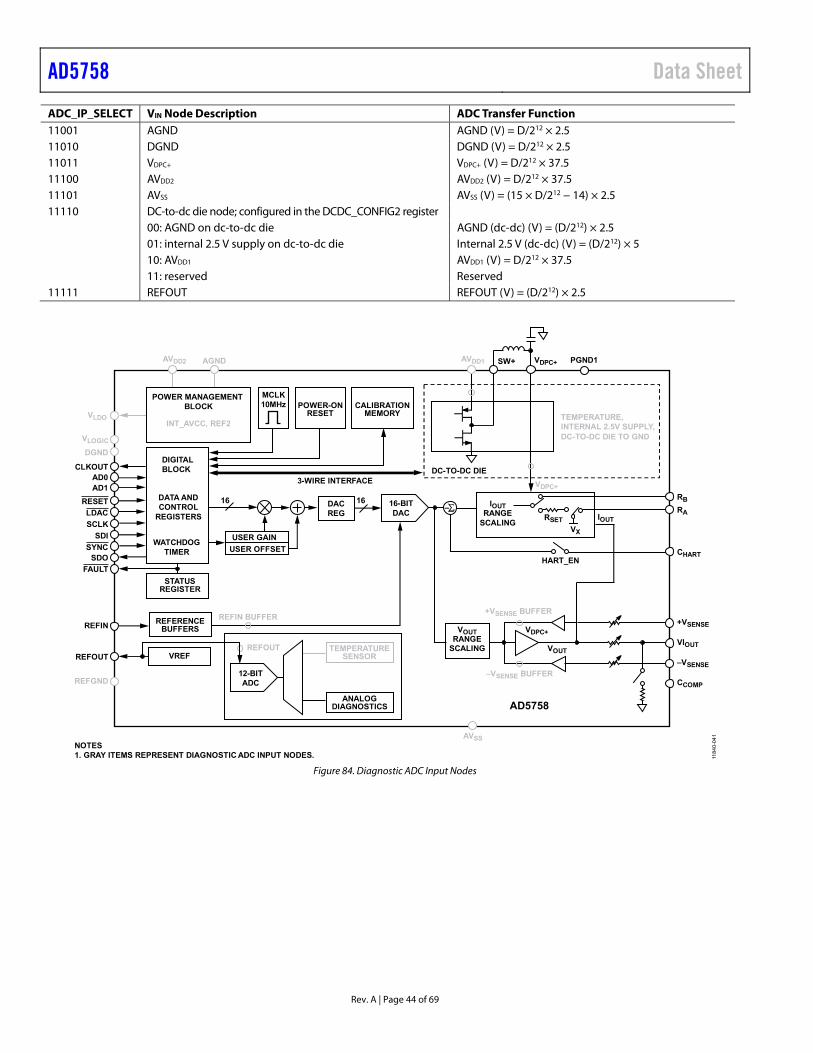
AD5758 Data Sheet
Rev. A | Page 44 of 69
ADC_IP_SELECT VIN Node Description ADC Transfer Function 11001 AGND AGND (V) = D/212 × 2.5 11010 DGND DGND (V) = D/212 × 2.5 11011 VDPC+ VDPC+ (V) = D/212 × 37.5 11100 AVDD2 AVDD2 (V) = D/212 × 37.5 11101 AVSS AVSS (V) = (15 × D/212 − 14) × 2.5 11110 DC-to-dc die node; configured in the DCDC_CONFIG2 register 00: AGND on dc-to-dc die AGND (dc-dc) (V) = (D/212) × 2.5 01: internal 2.5 V supply on dc-to-dc die Internal 2.5 V (dc-dc) (V) = (D/212) × 5 10: AVDD1 AVDD1 (V) = D/212 × 37.5 11: reserved Reserved 11111 REFOUT REFOUT (V) = (D/212) × 2.5
AD5758
AVSS
AGNDAVDD2
DGND
SCLKSDI
SDOSYNC
FAULT
DATA ANDCONTROL
REGISTERS
DIGITALBLOCK
WATCHDOGTIMER
STATUSREGISTER
POWER-ONRESET
REFERENCEBUFFERS
DACREG
VREF
CALIBRATIONMEMORY
VOUTRANGE
SCALINGREFOUT
REFIN
AD1AD0
16-BITDAC
1616
SW+ VDPC+
USER GAINUSER OFFSET
RB
+VSENSE
–VSENSE
CHART
IOUTRANGE
SCALINGIOUT
VOUT
DC-TO-DC DIECLKOUT
REFGND
NOTES1. GRAY ITEMS REPRESENT DIAGNOSTIC ADC INPUT NODES.
VLOGIC
VIOUT
CCOMP
PGND1
TEMPERATURESENSOR
ANALOGDIAGNOSTICS
12-BITADC
RESET
VDPC+
VLDO
VDPC+
MCLK10MHz
RSETVX
LDAC
HART_EN
3-WIRE INTERFACE
TEMPERATURE,INTERNAL 2.5V SUPPLY,DC-TO-DC DIE TO GND
–VSENSE BUFFER
+VSENSE BUFFERREFIN BUFFER
REFOUT
POWER MANAGEMENTBLOCK
INT_AVCC, REF2
AVDD1
RA
11840-041
–
Figure 84. Diagnostic ADC Input Nodes
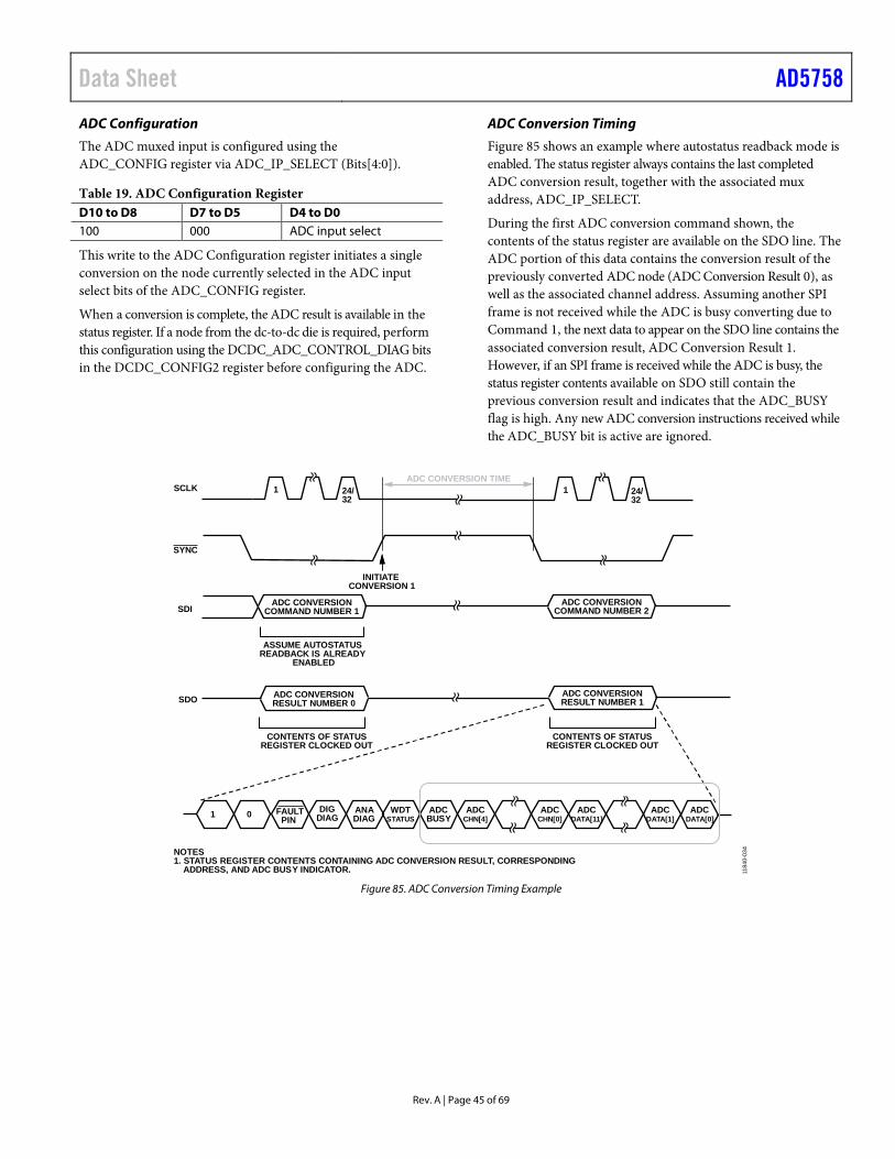
Data Sheet AD5758
Rev. A | Page 45 of 69
ADC Configuration
The ADC muxed input is configured using the ADC_CONFIG register via ADC_IP_SELECT (Bits[4:0]).
Table 19. ADC Configuration Register D10 to D8 D7 to D5 D4 to D0 100 000 ADC input select
This write to the ADC Configuration register initiates a single conversion on the node currently selected in the ADC input select bits of the ADC_CONFIG register.
When a conversion is complete, the ADC result is available in the status register. If a node from the dc-to-dc die is required, perform this configuration using the DCDC_ADC_CONTROL_DIAG bits in the DCDC_CONFIG2 register before configuring the ADC.
ADC Conversion Timing
Figure 85 shows an example where autostatus readback mode is enabled. The status register always contains the last completed ADC conversion result, together with the associated mux address, ADC_IP_SELECT.
During the first ADC conversion command shown, the contents of the status register are available on the SDO line. The ADC portion of this data contains the conversion result of the previously converted ADC node (ADC Conversion Result 0), as well as the associated channel address. Assuming another SPI frame is not received while the ADC is busy converting due to Command 1, the next data to appear on the SDO line contains the associated conversion result, ADC Conversion Result 1. However, if an SPI frame is received while the ADC is busy, the status register contents available on SDO still contain the previous conversion result and indicates that the ADC_BUSY flag is high. Any new ADC conversion instructions received while the ADC_BUSY bit is active are ignored.
SYNC
ASSUME AUTOSTATUSREADBACK IS ALREADY
ENABLED
SDI
CONTENTS OF STATUSREGISTER CLOCKED OUT
SDO
SCLK 24/32
1 24/32
1
CONTENTS OF STATUSREGISTER CLOCKED OUT
ADC CONVERSIONCOMMAND NUMBER 1
INITIATECONVERSION 1
ADC CONVERSION TIME
ADC CONVERSIONCOMMAND NUMBER 2
ADC CONVERSIONRESULT NUMBER 1
ADCBUSY
ADCDATA[1]
ADCDATA[11]
ADCCHN[0]
ADCCHN[4]
WDTSTATUS
ANADIAG
FAULT PIN
DIGDIAG1 0 ADC
DATA[0]
ADC CONVERSIONRESULT NUMBER 0
NOTES1. STATUS REGISTER CONTENTS CONTAINING ADC CONVERSION RESULT, CORRESPONDING
ADDRESS, AND ADC BUSY INDICATOR. 1 184
0-03
4
Figure 85. ADC Conversion Timing Example
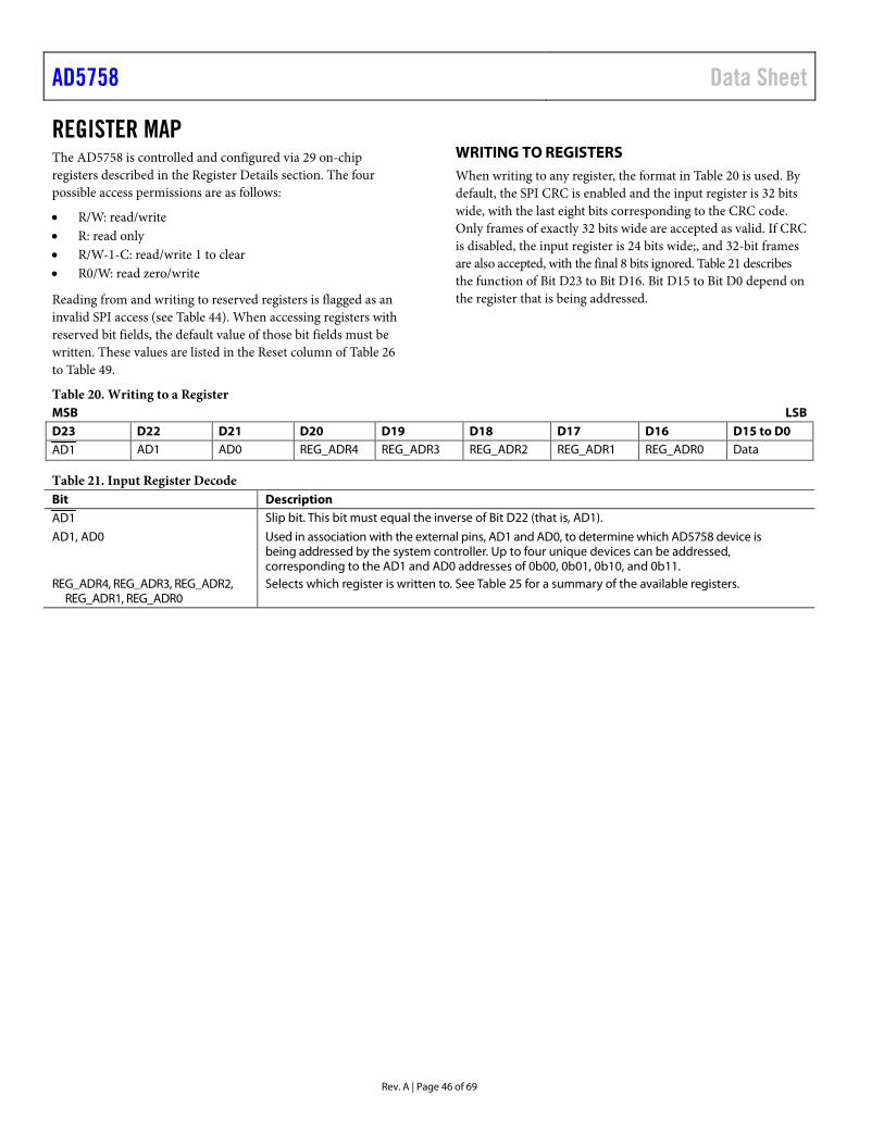
AD5758 Data Sheet
Rev. A | Page 46 of 69
REGISTER MAP The AD5758 is controlled and configured via 29 on-chip registers described in the Register Details section. The four possible access permissions are as follows:
• R/W: read/write • R: read only • R/W-1-C: read/write 1 to clear • R0/W: read zero/write
Reading from and writing to reserved registers is flagged as an invalid SPI access (see Table 44). When accessing registers with reserved bit fields, the default value of those bit fields must be written. These values are listed in the Reset column of Table 26 to Table 49.
WRITING TO REGISTERS When writing to any register, the format in Table 20 is used. By default, the SPI CRC is enabled and the input register is 32 bits wide, with the last eight bits corresponding to the CRC code. Only frames of exactly 32 bits wide are accepted as valid. If CRC is disabled, the input register is 24 bits wide;, and 32-bit frames are also accepted, with the final 8 bits ignored. Table 21 describes the function of Bit D23 to Bit D16. Bit D15 to Bit D0 depend on the register that is being addressed.
Table 20. Writing to a Register MSB LSB D23 D22 D21 D20 D19 D18 D17 D16 D15 to D0 AD1 AD1 AD0 REG_ADR4 REG_ADR3 REG_ADR2 REG_ADR1 REG_ADR0 Data
Table 21. Input Register Decode Bit Description AD1 Slip bit. This bit must equal the inverse of Bit D22 (that is, AD1).
AD1, AD0 Used in association with the external pins, AD1 and AD0, to determine which AD5758 device is being addressed by the system controller. Up to four unique devices can be addressed, corresponding to the AD1 and AD0 addresses of 0b00, 0b01, 0b10, and 0b11.
REG_ADR4, REG_ADR3, REG_ADR2, REG_ADR1, REG_ADR0
Selects which register is written to. See Table 25 for a summary of the available registers.

Data Sheet AD5758
Rev. A | Page 47 of 69
READING FROM REGISTERS The AD5758 has four options for readback mode that can be configured in the TWO_STAGE_READBACK_SELECT register (see Table 43). These options are as follows:
• Two stage readback • Autostatus readback • Shared SYNC autostatus readback • Echo mode
Two Stage Readback Mode
Two stage readback mode consists of a write to the TWO_ STAGE_READBACK_SELECT register to select the register location to be read back, followed by a NOP command. To perform a NOP command, write all zeros to Bits[D15:D0] of the NOP register. During the NOP command, the contents of the selected register are available on SDO in the format shown in Table 22. It is also possible to write a new two stage readback command during the second frame, such that the corresponding new data is available on SDO in the subsequent frame (see Figure 86). Bits[D31:D30] (or Bits[D23:D22], if SPI CRC is not enabled) = 0b10 are used as part of the synchronization during readback. The contents of the first write instruction to the TWO_ STAGE_READBACK_SELECT register is shown in Table 23.
Table 22. SDO Contents for Read Operation MSB LSB D23 to D22 D21 D20 to 16 D15 to D0 0b10 FAULT pin status Register address Data
Table 23. Reading from a Register Using Two Stage Readback Mode MSB LSB D23 D22 D21 D20 D19 D18 D17 D16 [D15:D5] D4 D3 D2 D1 D0 AD1 AD1 AD0 0x13 Reserved READBACK_SELECT[4:0]
SYNC
INPUT WORD SPECIFIESREGISTER TO BE READ
*NOPSDI
UNDEFINED SELECTED REGISTER DATACLOCKED OUT
SDO
SCLK 24/32
1 24/32
1
SELECTED REGISTER DATACLOCKED OUT
24/32
1
2-STAGE READBACK
*ALTERNATIVELY COULDWRITE ANOTHER
TWO-STAGE READBACK
NOP
1184
0-03
7
Figure 86. Two Stage Readback Example
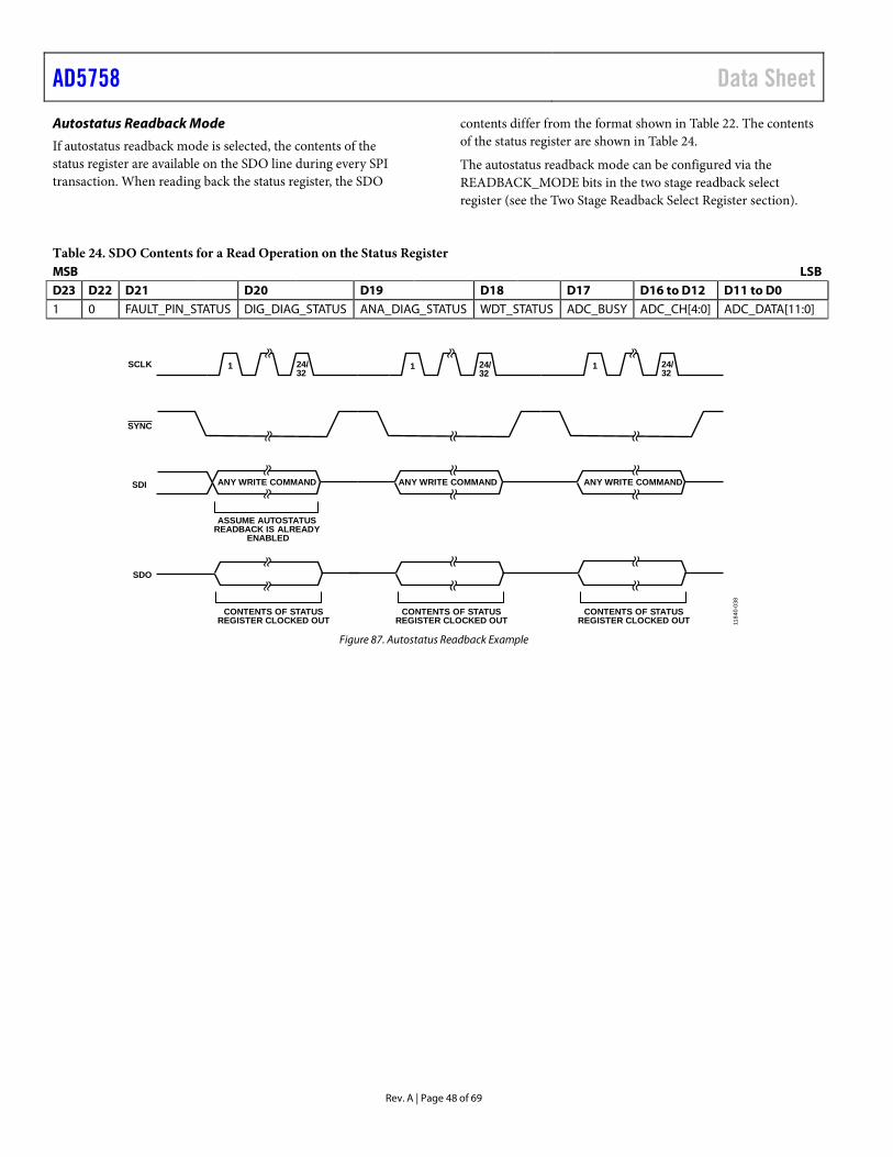
AD5758 Data Sheet
Rev. A | Page 48 of 69
Autostatus Readback Mode
If autostatus readback mode is selected, the contents of the status register are available on the SDO line during every SPI transaction. When reading back the status register, the SDO
contents differ from the format shown in Table 22. The contents of the status register are shown in Table 24.
The autostatus readback mode can be configured via the READBACK_MODE bits in the two stage readback select register (see the Two Stage Readback Select Register section).
Table 24. SDO Contents for a Read Operation on the Status Register MSB LSB D23 D22 D21 D20 D19 D18 D17 D16 to D12 D11 to D0 1 0 FAULT_PIN_STATUS DIG_DIAG_STATUS ANA_DIAG_STATUS WDT_STATUS ADC_BUSY ADC_CH[4:0] ADC_DATA[11:0]
SYNC
ASSUME AUTOSTATUSREADBACK IS ALREADY
ENABLED
SDI
CONTENTS OF STATUSREGISTER CLOCKED OUT
SDO
SCLK 24/32
1 24/32
1 24/32
1
CONTENTS OF STATUSREGISTER CLOCKED OUT
CONTENTS OF STATUSREGISTER CLOCKED OUT
ANY WRITE COMMAND ANY WRITE COMMAND ANY WRITE COMMAND
1184
0-03
8
Figure 87. Autostatus Readback Example
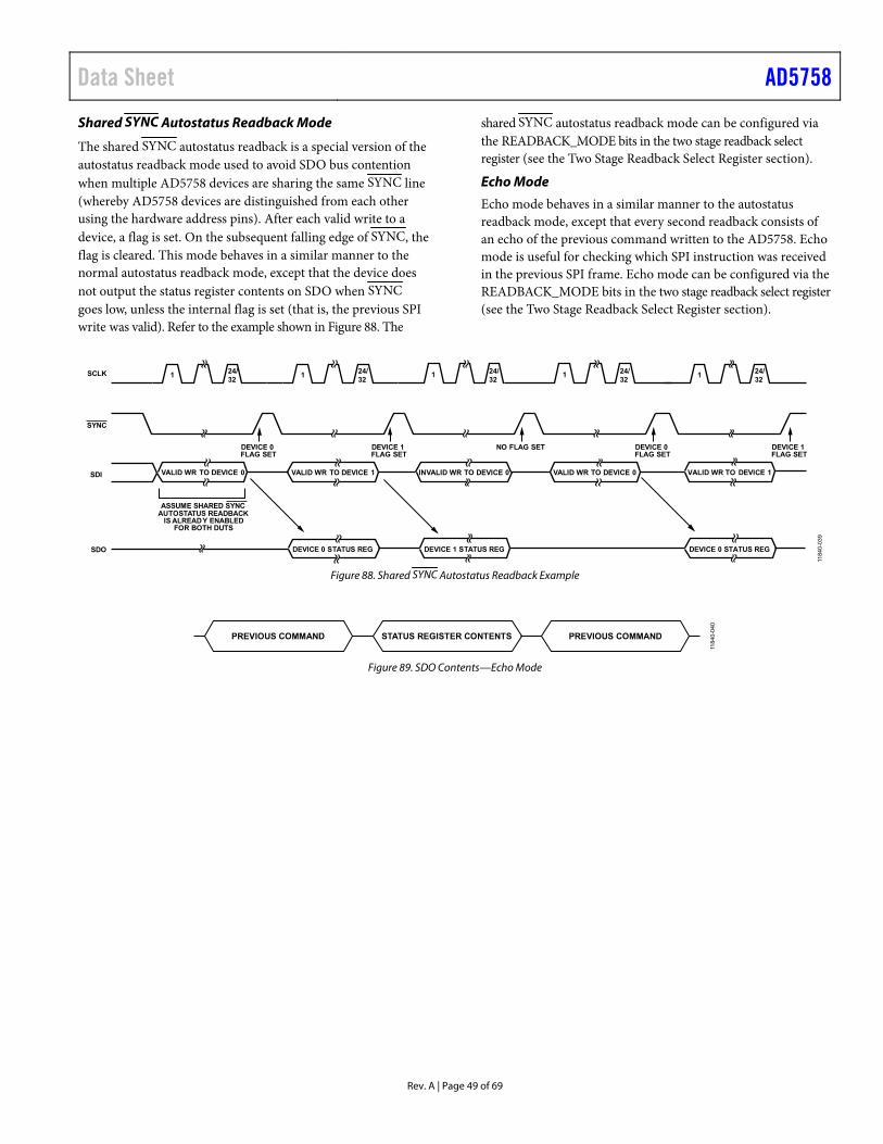
Data Sheet AD5758
Rev. A | Page 49 of 69
Shared SYNC Autostatus Readback Mode
The shared SYNC autostatus readback is a special version of the autostatus readback mode used to avoid SDO bus contention when multiple AD5758 devices are sharing the same SYNC line (whereby AD5758 devices are distinguished from each other using the hardware address pins). After each valid write to a device, a flag is set. On the subsequent falling edge of SYNC, the flag is cleared. This mode behaves in a similar manner to the normal autostatus readback mode, except that the device does not output the status register contents on SDO when SYNC goes low, unless the internal flag is set (that is, the previous SPI write was valid). Refer to the example shown in Figure 88. The
shared SYNC autostatus readback mode can be configured via the READBACK_MODE bits in the two stage readback select register (see the Two Stage Readback Select Register section).
Echo Mode
Echo mode behaves in a similar manner to the autostatus readback mode, except that every second readback consists of an echo of the previous command written to the AD5758. Echo mode is useful for checking which SPI instruction was received in the previous SPI frame. Echo mode can be configured via the READBACK_MODE bits in the two stage readback select register (see the Two Stage Readback Select Register section).
SYNC
ASSUME SHARED SYNCAUTOSTATUS READBACK
IS ALREADY ENABLEDFOR BOTH DUTS
SDI
SDO
SCLK 24/321 24/
321
VALID WR TO DEVICE 0
24/321 24/
321
DEVICE 0FLAG SET
VALID WR TO DEVICE 1
DEVICE 1FLAG SET
INVALID WR TO DEVICE 0 VALID WR TO DEVICE 0
DEVICE 0 STATUS REG DEVICE 1 STATUS REG
NO FLAG SET DEVICE 0FLAG SET
24/321
DEVICE 0 STATUS REG
VALID WR TO DEVICE 1
DEVICE 1FLAG SET
11840-039
Figure 88. Shared SYNC Autostatus Readback Example
PREVIOUS COMMAND STATUS REGISTER CONTENTS PREVIOUS COMMAND
11840-040
Figure 89. SDO Contents—Echo Mode

AD5758 Data Sheet
Rev. A | Page 50 of 69
PROGRAMMING SEQUENCE TO ENABLE THE OUTPUT To write to and set up the device from a power-on or reset condition, use the following procedure:
1. Perform a hardware or software reset and wait 100 µs. 2. Perform a calibration memory refresh by writing 0xFCBA to
the key register. Wait a minimum of 500 µs before proceeding to Step 3 to allow time for the internal calibrations to complete. As an alternative to waiting 500 µs for the refresh cycle to complete, poll the CAL_MEM_UNREFRESHED bit in the DIGITAL_DIAG_RESULTS register until it is 0.
3. Write 1 to Bit D13 in the DIGITAL_DIAG_RESULTS register to clear the RESET_OCCURRED flag.
4. If CLKOUT is required, configure and enable this feature via the GP_CONFIG1 register. It is important to configure this feature before enabling the dc-to-dc converter.
5. Write to the DCDC_CONFIG2 register to set the dc-to-dc current limit. Wait 300 µs to allow the 3-wire interface communication to complete. As an alternative to waiting 300 µs for the 3-wire interface communication to complete, poll the BUSY_3WI bit in the DCDC_CONFIG2 register until it is 0.
6. Write to the DCDC_CONFIG1 register to set up the dc-to-dc converter mode (thereby enabling the dc-to-dc converter). Wait 300 µs to allow the 3-wire interface communication to complete. As an alternative to waiting 300 µs to the 3-wire interface communication to complete, poll the BUSY_3WI bit in the DCDC_CONFIG2 register until it is 0.
7. Write to the DAC_CONFIG register to set the INT_EN bit (powers up the DAC and internal amplifiers without enabling the output) and configure the output range, internal/external RSET, and slew rate. Keep the OUT_EN bit disabled at this point. Wait 500 µs minimum before proceeding to Step 8 to allow time for the internal calibrations to complete. As an alternative to waiting 500 µs for the refresh cycle to
complete, poll the CAL_MEM_ UNREFRESHED bit in the DIGITAL_DIAG_RESULTS register until it is 0.
8. Write zero-scale DAC code to the DAC_INPUT register. (If a bipolar range was selected in Step 7, then a DAC code that represents a 0 mA/0 V output must be written to the DAC_INPUT register). It is important that this step be completed even if the contents of the DAC_INPUT register are not changing.
9. If LDAC functionality is being used, perform either a software or hardware LDAC command.
10. Rewrite the same word to the DAC_CONFIG register as in Step 7 except, this time, with the OUT_EN bit enabled. Allow 1.25 ms minimum between Step 6 and Step 9; this is the time from when the dc-to-dc is enabled to when the VIOUT output is enabled.
11. Write the required DAC code to the DAC_INPUT register.
An example configuration is shown in Figure 90.
Changing and Reprogramming the Range
After the output is enabled, use the following recommended steps when changing the output range:
1. Write to the DAC_INPUT register. Set the output to 0 mA or 0 V.
2. Write to the DAC_CONFIG register. Disable the output (OUT_EN = 0), and set the new output range. Keep the INT_EN bit set. Wait 500 µs minimum before proceeding to Step 3 to allow time for internal calibrations to complete.
3. Write Code 0x0000 (in the case of bipolar ranges, write Code 0x8000) to the DAC_INPUT register. It is important that this step be completed even if the contents of the DAC_INPUT register are not changing.
4. Reload the DAC_CONFIG register word from Step 2 except, this time, set the OUT_EN bit to 1 to enable the output.
5. Write the required DAC code to the DAC_INPUT register.

Data Sheet AD5758
Rev. A | Page 51 of 69
EXAMPLE CONFIGURATION TO ENABLE THE OUTPUT CORRECTLY
2. PERFORM CALIBRATIONMEMORY REFRESH
1. PERFORM HARDWARE ORSOFTWARE RESET
WRITE
5. SET UP THEDC‐TO‐DC CONVERTER
SETTINGS
WRITE
8. WRITE 0mV/0mADAC CODE
IS CAL_MEM_UNREFRESHED
== 0?IS WAIT
= 500µs?
WAIT = 0
NO WAIT = WAIT + 1NO
IS BUSY_3WI== 0?
IS WAIT= 300µs?
WAIT = 0
NO WAIT = WAIT + 1NO
ADDRESS[D23:D21] REGISTER ADDRESS[D20:D16] DATA[D15:D0]
SLIPBIT + AD[1:0] 0x08 0xFCBA
DUT ADDRESS[D23:D21] REGISTER ADDRESS[D20:D16] DATA[D15:D0]SLIPBIT + AD[1:0] 0x0C DC-TO-DC SETTINGS
4. CONFIGURE CLKOUTIF REQUIRED
WRITE DUT ADDRESS[D23:D21] REGISTER ADDRESS[D20:D16] DATA[D15:D0]SLIPBIT + AD[1:0] 0x09 GP CONFIG1 SETTINGS
3. CLEAR RESET_OCCURRED BIT
WRITE ADDRESS[D23:D21] REGISTER ADDRESS[D20:D16] DATA[D15:D0]SLIPBIT + AD[1:0] 0x14 D13 = 1
6. SET UP THEDC‐TO‐DC
CONVERTER MODE
WRITE
IS BUSY_3WI= 0?
IS WAIT= 300µs?
WAIT = 0
NO WAIT = WAIT + 1NO
ADDRESS[D23:D20] REGISTER ADDRESS[D20:D16] DATA[D15:D0]
SLIPBIT + AD[1:0] 0x0B DC-TO-DC MODE
7. CONFIGURE THE DAC(OUTPUT DISABLED)
WRITE
IS CAL_MEM_UNREFRESHED
= 0?IS WAIT
= 500µs?
WAIT = 0
NO WAIT = WAIT + 1NO
ADDRESS[D23:D21] REGISTER ADDRESS[D20:D16] DATA[D15:D0]
SLIPBIT + AD[1:0] 0x06 D6 = 0
WRITE DUT ADDRESS[D23:D21] REGISTER ADDRESS[D20:D16] DATA[D15:D0]SLIPBIT + AD[1:0] 0x01 DAC CODE
WRITE DUT ADDRESS[D23:D21] REGISTER ADDRESS[D19:D16] DATA[D15:D0]
SLIPBIT + AD[1:0] 0x07 0x1DAC9. PERFORM AN LDAC COMMAND
10. CONFIGURE THE DAC(OUTPUT ENABLED)
WRITE DUT ADDRESS[D23:D21] REGISTER ADDRESS[D19:D16] DATA[D15:D0]SLIPBIT + AD[1:0] 0x06
DAC CODEWRITE ADDRESS[D23:D21] REGISTER ADDRESS[D20:D16] DATA[D15:D0]
SLIPBIT + AD[1:0] 0x01
D6 = 1
11. WRITE THE REQUIREDDAC CODE
1184
0-11
8
Figure 90. Example Configuration to Enable the Output Correctly (CRC Disabled for Simplicity)

AD5758 Data Sheet
Rev. A | Page 52 of 69
REGISTER DETAILS
Table 25. Register Summary Address Name Description Reset Access 0x00 NOP NOP register. 0x000000 R 0x01 DAC_INPUT DAC input register. 0x010000 R/W 0x02 DAC_OUTPUT DAC output register. 0x020000 R 0x03 CLEAR_CODE Clear code register. 0x030000 R/W 0x04 USER_GAIN User gain register. 0x04FFFF R/W 0x05 USER_OFFSET User offset register. 0x058000 R/W 0x06 DAC_CONFIG DAC configuration register. 0x060C00 R/W 0x07 SW_LDAC Software LDAC register. 0x070000 R/W 0x08 Key Key register. 0x080000 R/W 0x09 GP_CONFIG1 General-Purpose Configuration 1 register. 0x090204 R/W 0x0A GP_CONFIG2 General-Purpose Configuration 2 register. 0x0A0200 R/W 0x0B DCDC_CONFIG1 DC-to-DC Configuration 1 register. 0x0B0000 R/W 0x0C DCDC_CONFIG2 DC-to-DC Configuration 2 register. 0x0C100 R/W 0x0D Reserved Reserved (do not write to this register). 0x0D0000 R/W 0x0E Reserved Reserved (do not write to this register). 0x0E0000 R/W 0x0F WDT_CONFIG WDT configuration register. 0x0F0009 R/W 0x10 DIGITAL_DIAG_CONFIG Digital diagnostic configuration register. 0x10005D R/W 0x11 ADC_CONFIG ADC configuration register. 0x110000 R/W 0x12 FAULT_PIN_CONFIG FAULT pin configuration register. 0x120000 R/W
0x13 TWO_STAGE_READBACK_SELECT Two stage readback select register. 0x130000 R/W 0x14 DIGITAL_DIAG_RESULTS Digital diagnostic results register. 0x14A000 R 0x15 ANALOG_DIAG_RESULTS Analog diagnostic results register. 0x150000 R 0x16 Status Status register. 0x100000 R 0x17 CHIP_ID Chip ID register. 0x170101 R 0x18 FREQ_MONITOR Frequency monitor register. 0x180000 R 0x19 Reserved Reserved. 0x190000 R 0x1A Reserved Reserved. 0x1A0000 R 0x1B Reserved Reserved. 0x1B0000 R 0x1C DEVICE_ID_3 Generic ID register. 0x1C0000 R
Data Sheet AD5758
Rev. A | Page 53 of 69
NOP Register
Address: 0x00, Reset: 0x000000, Name: NOP
Write 0x0000 to Bits[D15:D0] at this address to perform a no operation (NOP) command. Bits[15:0] of this register always read back as 0x0000.
Table 26. Bit Descriptions for NOP Bits Bit Name Description Reset Access 21 FAULT_PIN_STATUS The FAULT_PIN_STATUS bit reflects the current status of the FAULT pin. 0x0 R
[20:16] REGISTER_ADDRESS Register address. 0x0 R [15:0] NOP command Write 0x0000 to perform a NOP command. 0x0 R0/W
DAC Input Register
Address: 0x01, Reset: 0x010000, Name: DAC_INPUT
Bits[D15:D0] consists of the 16-bit data to be written to the DAC. If the LDAC pin is tied low (that is, active), the DAC_INPUT register contents are written directly to the DAC_OUTPUT register without any LDAC functionality dependence. If the LDAC pin is tied high, the contents of the DAC_INPUT register are written to the DAC_OUTPUT register when the LDAC pin is brought low or when the software LDAC command is written.
Table 27. Bit Descriptions for DAC_INPUT Bits Bit Name Description Reset Access 21 FAULT_PIN_STATUS The FAULT_PIN_STATUS bit reflects the inverted current status of the FAULT pin. 0x0 R
[20:16] REGISTER_ADDRESS Register address. 0x0 R [15:0] DAC_INPUT_DATA DAC input data. 0x0 R/W
DAC Output Register
Address: 0x02, Reset: 0x020000, Name: DAC_OUTPUT
DAC_OUTPUT is a read only register and contains the latest calibrated 16-bit DAC output value. If a clear event occurs due to a WDT fault, this register contains the clear code until the DAC is updated to another code.
Table 28. Bit Descriptions for DAC_OUTPUT Bits Bit Name Description Reset Access 21 FAULT_PIN_STATUS The FAULT_PIN_STATUS bit reflects the inverted current status of the FAULT pin. 0x0 R
[20:16] REGISTER_ADDRESS Register address. 0x0 R [15:0] DAC_OUTPUT_DATA DAC output data. For example, the last calibrated 16-bit DAC output value. 0x0 R
Clear Code Register
Address: 0x03, Reset: 0x030000, Name: CLEAR_CODE
When writing to the CLEAR_CODE register, Bits[D15:D0] consist of the clear code to which the DAC clears on the occurrence of a clear event (for example, a WDT fault). After a clear event, the DAC_INPUT register must be rewritten to with the 16-bit data to be written to the DAC, even if it is the same data as previously written before the clear event. Performing an LDAC write (either hardware or software) does not update the DAC_OUTPUT register to a new code until the DAC_INPUT register is first written to.
Table 29. Bit Descriptions for CLEAR_CODE Bits Bit Name Description Reset Access 21 FAULT_PIN_STATUS The FAULT_PIN_STATUS bit reflects the inverted current status of the FAULT pin. 0x0 R
[20:16] REGISTER_ADDRESS Register address. 0x0 R [15:0] CLEAR_CODE Clear code. The DAC clears to this code upon a clear event, for example, a WDT fault. 0x0 R/W

AD5758 Data Sheet
Rev. A | Page 54 of 69
User Gain Register
Address: 0x04, Reset: 0x04FFFF, Name: USER_GAIN
The 16-bit USER_GAIN register allows the user to adjust the gain of the DAC channel in steps of 1 LSB. The USER_GAIN register coding is straight binary. The default code is 0xFFFF. In theory, the gain can be tuned across the full range of the output. In practice, the maximum recommended gain trim is approximately 50% of the programmed range to maintain accuracy.
Table 30. Bit Descriptions for USER_GAIN Bits Bit Name Description Reset Access 21 FAULT_PIN_STATUS The FAULT_PIN_STATUS bit reflects the inverted current status of the FAULT pin. 0x0 R
[20:16] REGISTER_ADDRESS Register address. 0x0 R [15:0] USER_GAIN User gain correction code. 0xFFFF R/W
User Offset Register
Address: 0x05, Reset: 0x058000, Name: USER_OFFSET
The 16-bit USER_OFFSET register allows the user to adjust the offset of the DAC channel by −32,768 LSBs to +32,768 LSBs in steps of 1 LSB. The USER_OFFSET register coding is straight binary. The default code is 0x8000, which results in zero offset programmed to the output.
Table 31. Bit Descriptions for USER_OFFSET Bits Bit Name Description Reset Access 21 FAULT_PIN_STATUS The FAULT_PIN_STATUS bit reflects the inverted current status of the FAULT pin. 0x0 R
[20:16] REGISTER_ADDRESS Register address. 0x0 R [15:0] USER_OFFSET User offset correction code. 0x8000 R/W
DAC Configuration Register
Address: 0x06, Reset: 0x060C00, Name: DAC_CONFIG
This register configures the DAC (range, internal/external RSET, and output enable), enables the output stage circuitry, and configures the slew rate control function.
Table 32. Bit Descriptions for DAC_CONFIG Bits Bit Name Description Reset Access 21 FAULT_PIN_STATUS The FAULT_PIN_STATUS bit reflects the inverted current status of the FAULT pin. 0x0 R
[20:16] REGISTER_ADDRESS Register address. 0x0 R [15:13] SR_STEP Slew rate step. In conjunction with the slew rate clock, the slew rate step defines by
how much the output value changes at each update. Together, both parameters define the rate of change of the output value.
0x0 R/W
000: 4 LSB (default). 001: 12 LSB. 010: 64 LSB. 011: 120 LSB. 100: 256 LSB. 101: 500 LSB. 110: 1820 LSB. 111: 2048 LSB. [12:9] SR_CLOCK Slew rate clock. Slew rate clock defines the rate at which the digital slew is updated. 0x6 R/W 0000: 240 kHz. 0001: 200 kHz. 0010: 150 kHz. 0011: 128 kHz. 0100: 64 kHz. 0101: 32 kHz. 0110: 16 kHz (default). 0111: 8 kHz.

Data Sheet AD5758
Rev. A | Page 55 of 69
Bits Bit Name Description Reset Access 1000: 4 kHz. 1001: 2 kHz. 1010: 1 kHz. 1011: 512 Hz. 1100: 256 Hz. 1101: 128Hz. 1110: 64 Hz. 1111: 16 Hz. 8 SR_EN Enable slew rate control. 0x0 R/W 0: disable (default). 1: enable. 7 RSET_EXT_EN Enable external current setting resistor. 0x0 R/W 0: select internal RSET resistor (default). 1: select external RSET resistor. 6 OUT_EN Enable VIOUT. 0x0 R/W 0: disable VIOUT output (default). 1: enable VIOUT output. 5 INT_EN Enable internal buffers. 0x0 R/W 0: disable (default). 1: enable. Setting this bit powers up the DAC and internal amplifiers. Setting this bit
does not enable the output. It is recommended to set this bit and allow a >200 μs delay before enabling the output. This delay results in a reduced output enable glitch.
4 OVRNG_EN Enable 20% voltage overrange. 0x0 R/W 0: disable (default). 1: enable. [3:0] Range Select output range. Note that changing the contents of the range bits initiates an
internal calibration memory refresh and, therefore, a subsequent SPI write must not be performed until the CAL_MEM_UNREFRESHED bit in the DIGITAL_DIAG_RESULTS register returns to 0. Writes to invalid range codes are ignored.
0x0 R/W
0000: 0 V to 5 V voltage range (default). 0001: 0 V to 10 V voltage range. 0010: ±5 V voltage range. 0011: ±10 V voltage range. 1000: 0 mA to 20 mA current range. 1001: 0 mA to 24 mA current range. 1010: 4 mA to 20 mA current range. 1011: ±20 mA current range. 1100: ±24 mA current range. 1101: −1 mA to +22 mA current range.
Software LDAC Register
Address: 0x07, Reset: 0x070000, Name: SW_LDAC
Writing 0x1DAC to this register performs a software LDAC update on the device matching the ADDRESS bits within the SPI frame. If the GLOBAL_SW_LDAC bit in the GP_CONFIG2 register is set, the ADDRESS bits are ignored and all devices sharing the same SPI bus are updated via the SW_LDAC command. Bits[15:0] of this register always read back as 0x0000.
Table 33. Bit Descriptions for SW_LDAC Bits Bit Name Description Reset Access 21 FAULT_PIN_STATUS The FAULT_PIN_STATUS bit reflects the inverted current status of the FAULT pin. 0x0 R
[20:16] REGISTER_ADDRESS Register address. 0x0 R [15:0] LDAC_COMMAND Software LDAC. Write 0x1DAC to this register to perform a software LDAC instruction. 0x0 R0/W

AD5758 Data Sheet
Rev. A | Page 56 of 69
Key Register
Address: 0x08, Reset: 0x080000, Name: Key
This register accepts specific key codes to perform tasks such as calibration memory refresh and software reset. Bits[15:0] of this register always read back as 0x0000. All unlisted key codes are reserved.
Table 34. Bit Descriptions for Key Bits Bit Name Description Reset Access 21 FAULT_PIN_STATUS The FAULT_PIN_STATUS bit reflects the inverted current status of the FAULT pin. 0x0 R
[20:16] REGISTER_ADDRESS Register address. 0x0 R [15:0] KEY_CODE Key code. 0x0 R0/W 0x15FA: first of two keys to initiate a software reset. 0xAF51: second of two keys to initiate a software reset. 0x0D06: key to reset the WDT. 0xFCBA: key to initiate a calibration memory refresh to the shadow registers. This key
is only valid the first time it is run and has no effect if subsequent writes occur within a given system reset cycle.
General-Purpose Configuration 1 Register
Address: 0x09, Reset: 0x090204, Name: GP_CONFIG1
This register is used to configure functions such as the temperature comparator threshold and CLKOUT, as well as enabling other miscellaneous features.
Table 35. Bit Descriptions for GP_CONFIG1 Bits Bit Name Description Reset Access 21 FAULT_PIN_STATUS The FAULT_PIN_STATUS bit reflects the inverted current status of the FAULT pin. 0x0 R
[20:16] REGISTER_ADDRESS Register address. 0x0 R [15:14] Reserved Reserved. Do not alter the default value of this bit. 0x0 R [13:12] SET_TEMP_THRESHOLD Set the temperature comparator threshold value. 0x0 R/W 00: 142°C (default). 01: 127°C. 10: 112°C. 11: 97°C. [11:10] CLKOUT_CONFIG Configure the CLKOUT pin. 0x0 R/W 00: disable; no clock is output on the CLKOUT pin (default). 01: enable; clock is output on CLKOUT pin according to the CLKOUT_FREQ bits
(Bits[2:0]).
10: reserved (do not select this option). 11: reserved (do not select this option). [9:7] CLKOUT_FREQ Configure the frequency of CLKOUT. 0x4 R/W 000: 416 kHz. 001: 435 kHz. 010: 454 kHz. 011: 476 kHz. 100: 500 kHz (default). 101: 526 kHz. 110: 555 kHz. 111: 588 kHz. 6 HART_EN Enable the path to the CHART pin. 0x0 R/W 0: output of the DAC drives the output stage directly (default). 1: CHART path is coupled to the DAC output to allow a HART modem connection or
connection of a slew capacitor.

Data Sheet AD5758
Rev. A | Page 57 of 69
Bits Bit Name Description Reset Access 5 NEG_OFFSET_EN Enable negative offset in unipolar VOUT mode. When set, this bit offsets the
currently enabled unipolar output range by the value listed here. This bit is only applicable to the 0 V to 6 V range and the 0 V to 12 V range. The 0 V to 6 V range becomes −300 mV to 5.7 V; the 0 V to 12 V range becomes −400 mV to 11.6 V.
0x0 R/W
0: disable (default). 1: enable. 4 CLEAR_NOW_EN Enables clear to occur immediately, even if the output slew feature is currently enabled. 0x0 R/W 0: disable (default). 1: enable. 3 SPI_DIAG_QUIET_EN Enable SPI diagnostic quiet mode. When this bit is enabled, SPI_CRC_ERR, SLIPBIT_ERR,
and SCLK_COUNT_ERR are not included in the logical OR calculation, which creates the DIG_DIAG_STATUS bit in the status register. They are also masked from affecting the FAULT pin if this bit is set.
0x0 R/W
0: disable (default). 1: enable. 2 OSC_STOP_DETECT_EN Enable automatic 0x07DEAD code on SDO if the internal oscillator (MCLK) stops. 0x1 R/W 0: disable. 1: enable (default). 1 Reserved Reserved. Do not alter the default value of this bit. 0x0 R/W 0 Reserved Reserved. Do not alter the default value of this bit. 0x0 R/W
General-Purpose Configuration 2 Register
Address: 0x0A, Reset: 0x0A0200, Name: GP_CONFIG2
This register is used to configure and enable functions such as the voltage comparators and the global software LDAC.
Table 36. Bit Descriptions for GP_CONFIG2 Bits Bit Name Description Reset Access 21 FAULT_PIN_STATUS The FAULT_PIN_STATUS bit reflects the inverted current status of the
FAULT pin. 0x0 R
[20:16] REGISTER_ADDRESS Register address. 0x0 R 15 Reserved Reserved. Do not alter the default value of this bit. 0x0 R0 [14:13] COMPARATOR_CONFIG Enable/disable the voltage comparator inputs for test purposes. The
temperature comparator is permanently enabled. See the Background Supply and Temperature Monitoring section.
0x0 R/W
00: disable voltage comparators (default). 01: reserved. 10: reserved. 11: enable voltage comparators. The INT_EN bit in the DAC_CONFIG register
must be set for the REFIN buffer to be powered up and this node available to the REFIN comparator.
12 Reserved Reserved. Do not alter the default value of this bit. 0x0 R/W 11 Reserved Reserved. Do not alter the default value of this bit. 0x0 R/W 10 GLOBAL_SW_LDAC When enabled, the address bits are ignored when performing a software
LDAC command, enabling multiple devices to be simultaneously updated using one SW_LDAC command.
0x0 R/W
0: disable (default). 1: enable. 9 FAULT_TIMEOUT Enable reduced fault detect timeout. This bit configures the delay from when
the analog block indicates a VIOUT fault has been detected to the associated change of the relevant bit in the ANALOG_DIAG_RESULTS register. This feature provides flexibility to accommodate a variety of output load values.
0x1 R/W
0: fault detect timeout = 25 ms. 1: fault detect timeout = 6.5 ms (default). [8:5] Reserved Reserved. Do not alter the default value of these bits. 0x0 R/W

AD5758 Data Sheet
Rev. A | Page 58 of 69
Bits Bit Name Description Reset Access 4 Reserved Reserved. Do not alter the default value of this bit. 0x0 R/W 3 Reserved Reserved. Do not alter the default value of this bit. 0x0 R/W 2 Reserved Reserved. Do not alter the default value of this bit. 0x0 R/W 1 Reserved Reserved. Do not alter the default value of this bit. 0x0 R/W 0 Reserved Reserved. Do not alter the default value of this bit. 0x0 R/W
DC-to-DC Configuration 1 Register
Address: 0x0B, Reset: 0x0B0000, Name: DCDC_CONFIG1
This register is used to configure the dc-to-dc controller mode.
Table 37. Bit Descriptions for DCDC_CONFIG1 Bits Bit Name Description Reset Access 21 FAULT_PIN_STATUS The FAULT_PIN_STATUS bit reflects the inverted current status of the FAULT pin. 0x0 R
[20:16] REGISTER_ADDRESS Register address. 0x0 R [15:8] Reserved Reserved. Do not alter the default value of these bits. 0x0 R0 7 Reserved Reserved. Do not alter the default value of this bit. 0x0 R/W [6:5] DCDC_MODE These two bits configure the dc-to-dc converters. 0x0 R/W 00: DC-to-DC converter powered off (default). 01: DPC current mode. The positive DPC rail tracks the headroom of the current
output buffer.
10: DPC voltage mode. The positive DPC rail is regulated to 15 V with respect to −VSENSE.
11: PPC current mode. VDPC+ is regulated to a user programmable level between 5 V and 25.677 V (depending on the DCDC_VPROG bits, Bits[4:0]) with respect to −VSENSE. The ENABLE_PPC_BUFFERS bit (Bit 11 in the ADC_CONFIG register) must be set prior to enabling PPC current mode.
[4:0] DCDC_VPROG DC-to-dc programmed voltage in PPC mode. VDPC+ is regulated to a user programmable level between 5 V (0b00000) and 25.677 V (0b11111), in steps of 0.667 V. VDPC+ is regulated with respect to −VSENSE.
0x0 R/W
DC-to-DC Configuration 2 Register
Address: 0x0C, Reset: 0x0C0100, Name: DCDC_CONFIG2
This register configures various dc-to-dc die features, such as the dc-to-dc converter current limit and the dc-to-dc die node, to be multiplexed to the ADC.
Table 38. Bit Descriptions for DCDC_CONFIG2 Bits Bit Name Description Reset Access 21 FAULT_PIN_STATUS The FAULT_PIN_STATUS bit reflects the inverted current status of the
FAULT pin. 0x0 R
[20:16] REGISTER_ADDRESS Register address. 0x0 R [15:13] Reserved Reserved. Do not alter the default value of these bits. 0x0 R0 12 BUSY_3WI Three-wire interface busy indicator. 0x0 R 0: 3-wire interface not currently active. 1: 3-wire interface busy. 11 INTR_SAT_3WI Three-wire interface saturation flag. This flag is set to 1 when the
interrupt detection circuitry is automatically disabled due to six consecutive interrupt signals. A write to either of the dc-to-dc configuration registers clears this bit to 0.
0x0 R
10 DCDC_READ_COMP_DIS Disable 3-wire interface read and compare cycle. This read and compare cycle ensures that the contents of the copy of the dc-to-dc configuration registers on the main die match the contents on the dc-to-dc die.
0x0 R/W
0: enable automatic read and compare cycle (default).
Data Sheet AD5758
Rev. A | Page 59 of 69
Bits Bit Name Description Reset Access 1: when set, this bit disables the automatic read and compare cycle
after each 3-wire interface write.
[9:8] Reserved Reserved. Do not alter the default value of these bits. 0x1 R/W 7 VIOUT_OV_ERR_DEGLITCH Adjust the deglitch time on VIOUT overvoltage error flag. 0x0 R/W 0: deglitch time set to 1.02 ms (default). 1: deglitch time set to 128 μs. 6 VIOUT_PULLDOWN_EN Enable the 30 kΩ resistor to ground on VIOUT. 0x0 R/W 0: disable (default). 1: enable. [5:4] DCDC_ADC_CONTROL_DIAG Select which dc-to-dc die node is multiplexed to the ADC on the
main die. 0x0 R/W
00: AGND on dc-to-dc die. 01: internal 2.5 V supply on dc-to-dc die. 10: AVDD1. 11: reserved (do not select this option). [3:1] DCDC_ILIMIT These three bits set the dc-to-dc converter current limit. 0x0 R/W 000: 150 mA (default). 001: 200 mA. 010: 250 mA. 011: 300 mA. 100: 350 mA. 101: 400 mA. 110: 400 mA. 111: 400 mA. 0 Reserved Reserved. Do not alter the default value of this bit. 0x0 R/W
Watchdog Timer (WDT) Configuration Register
Address: 0x0F, Reset: 0x0D0009, Name: WDT_CONFIG
This register configures the WDT timeout values. This register also configures the WDT setup in terms of acceptable resets and the resulting response to a WDT fault (for example, clear the output or reset the device).
Table 39. Bit Descriptions for WDT_CONFIG Bits Bit Name Description Reset Access 21 FAULT_PIN_STATUS The FAULT_PIN_STATUS bit reflects the inverted current status of the FAULT pin. 0x0 R
[20:16] REGISTER_ADDRESS Register address. 0x0 R [15:11] Reserved Reserved. Do not alter the default value of these bits. 0x0 R 10 CLEAR_ON_WDT_FAIL Enable clear on WDT fault. If the WDT times out, a clear event occurs, whereby the
output is loaded with the clear code stored in the CLEAR_CODE register. 0x0 R/W
0: disable (default). 1: enable. 9 RESET_ON_WDT_FAIL Enable a software reset to automatically occur if the WDT times out. 0x0 R/W 0: disable (default). 1: enable. 8 KICK_ON_VALID_WRITE Enable any valid SPI command to reset the WDT. Any active WDT error flags must
be cleared before the WDT can be restarted. 0x0 R/W
0: disable (default). 1: enable. 7 Reserved Reserved. Do not alter the default value of this bit. 0x0 R/W 6 WDT_EN Enables the WDT, then starts the WDT, assuming there are no active WDT fault flags. 0x0 R/W 0: disable (default). 1: enable. [5:4] Reserved Reserved. Do not alter the default value of these bits. 0x0 R/W
AD5758 Data Sheet
Rev. A | Page 60 of 69
Bits Bit Name Description Reset Access [3:0] WDT_TIMEOUT Set the WDT timeout value. Setting WDT_TIMEOUT to a binary value beyond
0b1010 results in the default setting of 1 sec. 0x9 R/W
0000: 1 ms. 0001: 5 ms. 0010: 10 ms. 0011: 25 ms. 0100: 50 ms. 0101: 100 ms. 0110: 250 ms. 0111: 500 ms. 1000: 750 ms. 1001: 1 sec (default). 1010: 2 sec.
Digital Diagnostic Configuration Register Address: 0x10, Reset: 0x10005D, Name: DIGITAL_DIAG_CONFIG
This register configures various digital diagnostic features of interest for a particular application.
Table 40. Bit Descriptions for DIGITAL_DIAG_CONFIG Bits Bit Name Description Reset Access 21 FAULT_PIN_STATUS The FAULT_PIN_STATUS bit reflects the inverted current status of the FAULT pin. 0x0 R
[20:16] REGISTER_ADDRESS Register address. 0x0 R [15:9] Reserved Reserved. Do not alter the default value of these bits. 0x0 R0 [8:7] Reserved Reserved. Do not alter the default value of these bits. 0x0 R/W 6 DAC_LATCH_MON_EN Enable a diagnostic monitor on the DAC latches. This feature monitors the actual
digital code driving the DAC and compares it with the digital code generated within the digital block. Any difference between the two codes causes the DAC_LATCH_MON_ERR flag to be set in the DIGITAL_DIAG_RESULTS register.
0x1 R/W
0: disable. 1: enable (default). 5 Reserved Reserved. Do not alter the default value of this bit. 0x0 R/W 4 INVERSE_DAC_CHECK_EN Enable check for DAC code vs. inverse DAC code error. 0x1 R/W 0: disable. 1: enable (default). 3 CAL_MEM_CRC_EN Enable CRC of calibration memory on a calibration memory refresh. 0x1 R/W 0: disable. 1: enable (default). 2 FREQ_MON_EN Enable the internal frequency monitor on the internal oscillator (MCLK). 0x1 R/W 0: disable. 1: enable (default). 1 Reserved Reserved. Do not alter the default value of this bit. 0x0 R/W 0 SPI_CRC_EN Enable SPI CRC function. 0x1 R/W 0: disable. 1: enable (default).

Data Sheet AD5758
Rev. A | Page 61 of 69
ADC Configuration Register
Address: 0x11, Reset: 0x110000, Name: ADC_CONFIG
This register configures the ADC into one of four modes of operation: key sequencing, automatic sequencing, single immediate conversion of the currently selected ADC_IP_SELECT node, or single-key conversion.
Table 41. Bit Descriptions for ADC_CONFIG Bits Bit Name Description Reset Access 21 FAULT_PIN_STATUS The FAULT_PIN_STATUS bit reflects the inverted current status of the FAULT pin. 0x0 R
[20:16] REGISTER_ADDRESS Register address. Do not alter the default value. 0x0 R [15:12] Reserved Reserved. Do not alter the default value of these bits. 0x0 R/W 11 ENABLE_PPC_BUFFERS Enable the sense buffers for PPC mode. 0x0 R/W [10:8] SEQUENCE_COMMAND ADC sequence command bits. 0x0 R/W 000: reserved (do not select this option). 001: reserved (do not select this option). 010: reserved (do not select this option). 011: reserved (do not select this option). 100: initiate a single conversion on the ADC_IP_SELECT (Bits[4:0]) input. 101: reserved (do not select this option). 110: reserved (do not select this option). 111: reserved (do not select this option). [7:5] Reserved Reserved. Do not alter the default value of these bits. 0x0 R/W [4:0] ADC_IP_SELECT Select which node to multiplex to the ADC. All unlisted 5-bit codes are reserved
and return an ADC result of zero. 0x0 R/W
00000: Main die temperature. 00001: DC-to-dc die temperature. 00010: Reserved (do not select this option). 00011: REFIN. The INT_EN bit in the DAC_CONFIG register must be set for the REFIN
buffer to be powered up and this node to be available to the ADC.
00100: REF2; internal 1.23 V reference voltage. 00101: Reserved (do not select this option). 00110: Reserved (do not select this option). 01100: Reserved (do not select this option). 01101: Voltage on the +VSENSE buffer output. 01110: Voltage on the −VSENSE buffer output 10000: Reserved (do not select this option). 10001: Reserved (do not select this option). 10010: Reserved (do not select this option). 10011: Reserved (do not select this option). 10100: INT_AVCC. 10101: VLDO. 10110: VLOGIC. 11000: REFGND. 11001: AGND. 11010: DGND. 11011: VDPC+. 11100: AVDD2. 11101: AVSS. 11110: DC-to-dc die node; configured in the DCDC_CONFIG2 register. 11111: REFOUT.
AD5758 Data Sheet
Rev. A | Page 62 of 69
FAULT Pin Configuration Register
Address: 0x12, Reset: 0x120000, Name: FAULT_PIN_CONFIG
This register is used to mask particular fault bits from the FAULT pin, if so desired.
Table 42. Bit Descriptions for FAULT_PIN_CONFIG Bits Bit Name Description Reset Access 21 FAULT_PIN_STATUS The FAULT_PIN_STATUS bit reflects the inverted current status of the FAULT pin. 0x0 R
[20:16] REGISTER_ADDRESS Register address. 0x0 R 15 INVALID_SPI_ACCESS_ERR If this bit is set, do not map the INVALID_SPI_ACCESS_ERR fault flag to the
FAULT pin. 0x0 R/W
14 VIOUT_OV_ERR If this bit is set, do not map the VIOUT_OV_ERR fault flag to the FAULT pin. 0x0 R/W
13 Reserved Reserved. Do not alter the default value of this bit. 0x0 R/W 12 INVERSE_DAC_CHECK_ERR If this bit is set, do not map the INVERSE_DAC_CHECK_ERR flag to the FAULT pin. 0x0 R/W
11 Reserved Reserved. Do not alter the default value of this bit. 0x0 R/W 10 OSCILLATOR_STOP_DETECT If this bit is set, do not map the clock stop error to the FAULT pin. 0x0 R/W
9 DAC_LATCH_MON_ERR If this bit is set, do not map the DAC_LATCH_MON_ERR fault flag to the FAULT pin. 0x0 R/W
8 WDT_ERR If this bit is set, do not map the WDT_ERR flag to the FAULT pin. 0x0 R/W
7 SLIPBIT_ERR If this bit is set, do not map the SLIPBIT_ERR error flag to the FAULT pin. 0x0 R/W
6 SPI_CRC_ERR If this bit is set, do not map the SPI_CRC_ERR error flag to the pin. 0x0 R/W 5 Reserved Reserved. Do not alter the default value of this bit. 0x0 R/W 4 DCDC_P_SC_ERR If this bit is set, do not map the positive rail dc-to-dc short circuit error flag to the
FAULT pin. 0x0 R/W
3 IOUT_OC_ERR If this bit is set, do not map the current output open-circuit error flag to the FAULT pin. 0x0 R/W
2 VOUT_SC_ERR If this bit is set, do not map the voltage output short-circuit error flag to the FAULT pin. 0x0 R/W
1 DCDC_DIE_TEMP_ERR If this bit is set, do not map the dc-to-dc die temperature error flag to the FAULT pin. 0x0 R/W
0 MAIN_DIE_TEMP_ERR If this bit is set, do not map the main die temperature error flag to the FAULT pin. 0x0 R/W
Two Stage Readback Select Register
Address: 0x13, Reset: 0x130000, Name: TWO_STAGE_READBACK_SELECT
This register selects the address of the register required for a two stage readback operation. The address of the register selected for readback is stored in Bits[D4:D0].
Table 43. Bit Descriptions for TWO_STAGE_READBACK_SELECT Bits Bit Name Description Reset Access 21 FAULT_PIN_STATUS The FAULT_PIN_STATUS bit reflects the inverted current status of the FAULT pin. 0x0 R
[20:16] REGISTER_ADDRESS Register address. 0x0 R [15:7] Reserved Reserved. 0x0 R [6:5] READBACK_MODE These bits control the SPI readback mode. 0x0 R/W 0: two stage SPI readback mode (default). 01: autostatus readback mode: the status register contents are shifted out on SDO for
every SPI frame.
10: shared SYNC autostatus readback mode. This mode allows the use of a shared SYNC line on multiple devices (distinguished using the hardware address pins). After each valid write to a device, a flag is set. This mode behaves similar to the normal autostatus read-back mode, except that the device does not output the status register contents on SDO as SYNC goes low, unless the internal flag is set (that is, the previous SPI write is valid).
11: the status register contents and the previous SPI frame instruction are alternately available on SDO.
[4:0] READBACK_SELECT Select readback address for a two stage readback. 0x0 R/W 0x00: NOP register (default). 0x01: DAC_INPUT register. 0x02: DAC_OUTPUT register.
Data Sheet AD5758
Rev. A | Page 63 of 69
Bits Bit Name Description Reset Access 0x03: CLEAR_CODE register. 0x04: USER_GAIN register. 0x05: USER_OFFSET register. 0x06: DAC_CONFIG register. 0x07: SW_LDAC register. 0x08: Key register. 0x09: GP_CONFIG1 register. 0x0A: GP_CONFIG2 register. 0x0B: DCDC_CONFIG1 register. 0x0C: DCDC_CONFIG2 register. 0x0D: Reserved (do not select this option). 0x0E: Reserved (do not select this option). 0x0F: WDT_CONFIG register. 0x10: DIGITAL_DIAG_CONFIG register. 0x11: ADC_CONFIG register. 0x12: FAULT_PIN_CONFIG register. 0x13: TWO_STAGE_READBACK_SELECT register. 0x14: DIGITAL_DIAG_RESULTS register. 0x15: ANALOG_DIAG_RESULTS register. 0x16: Status register. 0x17: CHIP_ID register. 0x18: FREQ_MONITOR register. 0x19: Reserved (do not select this option). 0x1A: Reserved (do not select this option). 0x1B: Reserved (do not select this option). 0x1C: DEVICE_ID_3 register.
Digital Diagnostic Results Register
Address: 0x14, Reset: 0x14A000, Name: DIGITAL_DIAG_RESULTS
This register contains an error flag for the on-chip digital diagnostic features, most of which are configurable using the digital diagnostic configuration register. This register also contains a flag to indicate that a reset occurred, as well as a flag to indicate that the calibration memory has not refreshed or an invalid SPI access attempted. With the exception of the CAL_MEM_UNREFRESHED and SLEW_BUSY flags, all of these flags require a 1 to be written to them to update them to their current value. The CAL_MEM_UNREFRESHED and SLEW_BUSY flags automatically clear when the calibration memory refresh or output slew, respectively, is complete. When the corresponding enable bits in the DIGITAL_DIAG_CONFIG register are not enabled, the respective flag bits read as zero.
Table 44. Bit Descriptions for DIGITAL_DIAG_RESULTS Bits Bit Name Description Reset Access 21 FAULT_PIN_STATUS The FAULT_PIN_STATUS bit reflects the inverted current status of the FAULT pin. 0x0 R
[20:16] REGISTER_ADDRESS Register address. 0x0 R 15 CAL_MEM_UNREFRESHED Calibration memory unrefreshed flag. Note that modifying the range bits in
the DAC_CONFIG register also initiates a calibration memory refresh, which asserts this bit. Unlike the R/W-1-C bits in this register, this bit is automatically cleared after the calibration memory refresh completes.
0x1 R
0: calibration memory is refreshed. 1: calibration memory is unrefreshed (default on power-up). Note that this
bit asserts if the range bits are modified in the DAC_CONFIG register.
14 SLEW_BUSY This flag is set to 1 when the DAC is actively slewing. Unlike the R/W-1-C bits in this register, this bit is automatically cleared when slewing is complete.
0x0 R
13 RESET_OCCURRED This bit flags that a reset occurred (default on power-up is therefore Logic 1). 0x1 R/W-1-C 12 ERR_3WI This bit flags an error in the interdie 3-wire interface communications. 0x0 R/W-1-C 11 WDT_ERR This bit flags a WDT fault. 0x0 R/W-1-C 10 Reserved Reserved. 0x0 R/W-1-C
AD5758 Data Sheet
Rev. A | Page 64 of 69
Bits Bit Name Description Reset Access 9 3WI_RC_ERR This bit flags an error if the 3-wire read and compare process is enabled and
a parity error occurs. 0x0 R/W-1-C
8 DAC_LATCH_MON_ERR This bit flags if the output of the DAC latches does not match the input. 0x0 R/W-1-C 7 Reserved Reserved. 0x0 R/W-1-C 6 INVERSE_DAC_CHECK_ERR This bit flags if a fault it detected between the DAC code driven by the digital
core and an inverted copy. 0x0 R/W-1-C
5 CAL_MEM_CRC_ERR This bit flags a CRC error for the CRC calculation of the calibration memory upon refresh.
0x0 R/W-1-C
4 INVALID_SPI_ACCESS_ERR This bit flags if an invalid SPI access is attempted, such as writing to or reading from an invalid or reserved address. This bit also flags if an SPI write is attempted directly after powering up but before a calibration memory refresh is performed or if an SPI write is attempted while a calibration memory refresh is in progress. Performing a two stage readback is permitted during a calibration memory refresh and does not cause this flag to set. Attempting to write to a read only register also causes this bit to assert.
0x0 R/W-1-C
3 Reserved Reserved. 0x0 R/W-1-C 2 SCLK_COUNT_ERR This bit flags an SCLK falling edge count error. 32 clocks are required if SPI
CRC is enabled and 24 clocks or 32 clocks are required if SPI CRC is not enabled. 0x0 R/W-1-C
1 SLIPBIT_ERR This bit flags an SPI frame slip bit error, that is, the MSB of the SPI word is not equal to the inverse of MSB − 1.
0x0 R/W-1-C
0 SPI_CRC_ERR This bit flags an SPI CRC error. 0x0 R/W-1-C
Analog Diagnostic Results Register
Address: 0x15, Reset: 0x150000, Name: ANALOG_DIAG_RESULTS
This register contains an error flag corresponding to the four voltage nodes (VLDO, INT_AVCC, REFIN, and REFOUT) monitored in the background by comparators, as well as a flag for each die temperature, which is also monitored by comparators. Voltage output short circuit, current output open circuit and dc-to-dc error flags are also contained in this register. Like the DIGITAL_DIAG_RESULTS register, all of the flags contained in this register require a 1 to be written to them to update or clear them. When the corresponding diagnostic features are not enabled, the respective error flags are read as zero.
Table 45. Bit Descriptions for ANALOG_DIAG_RESULTS Bits Bit Name Description Reset Access 21 FAULT_PIN_STATUS The FAULT_PIN_STATUS bit reflects the inverted current status of the FAULT pin. 0x0 R
[20:16] REGISTER_ADDRESS Register address. 0x0 R [15:14] Reserved Reserved. 0x0 R0 13 VIOUT_OV_ERR This bit flags if the voltage at the VIOUT pin goes outside of the VDPC+ rail or AVSS rail. 0x0 R/W-1-C 12 Reserved Reserved. 0x0 R/W-1-C 11 DCDC_P_SC_ERR This bit flags a dc-to-dc short-circuit error for the positive rail dc-to-dc circuit. 0x0 R/W-1-C 10 Reserved Reserved. 0x0 R/W-1-C 9 DCDC_P_PWR_ERR This bit flags a dc-to-dc regulation fault, that is, the dc-to-dc circuitry cannot reach
the target VDPC+ voltage due to an insufficient AVDD1 voltage. 0x0 R/W-1-C
8 Reserved Reserved. 0x0 R/W-1-C 7 IOUT_OC_ERR This bit flags a current output open circuit error. This error bit is set in the case of a
current output open circuit and in the case where there is insufficient headroom available to the internal current output driver circuitry to provide the programmed output current.
0x0 R/W-1-C
6 VOUT_SC_ERR This bit flags a voltage output short-circuit error. 0x0 R/W-1-C 5 DCDC_DIE_TEMP_ERR This bit flags an overtemperature error for the dc-to-dc die. 0x0 R/W-1-C 4 MAIN_DIE_TEMP_ERR This bit flags an overtemperature error for the main die. 0x0 R/W-1-C 3 REFOUT_ERR This bit flags that the REFOUT node is outside of the comparator threshold levels
or if its short-circuit current limit occurs. 0x0 R/W-1-C
2 REFIN_ERR This bit flags that the REFIN node is outside of the comparator threshold levels. 0x0 R/W-1-C 1 INT_AVCC_ERR This bit flags that the INT_AVCC node is outside of the comparator threshold
levels. 0x0 R/W-1-C
Data Sheet AD5758
Rev. A | Page 65 of 69
Bits Bit Name Description Reset Access 0 VLDO_ERR This bit flags that the VLDO node is outside of the comparator threshold levels or if
its short-circuit current limit occurs. 0x0 R/W-1-C
Status Register
Address: 0x16, Reset: 0x100000, Name: Status
This register contains ADC data and status bits, as well as the WDT, OR'd analog and digital diagnostics, and the FAULT pin status bits.
Table 46. Bit Descriptions for Status Bits Bit Name Description Reset Access 21 FAULT_PIN_STATUS The FAULT_PIN_STATUS bit reflects the inverted current status of the FAULT pin. 0x0 R
20 DIG_DIAG_STATUS This bit represents the result of a logical OR of the contents of Bits[15:0] in the DIGITAL_DIAG_RESULTS register, with the exception of the SLEW_BUSY bit. Therefore, if any of these bits are high, the DIG_DIAG_STATUS bit is high. Note that this bit is high on power-up due to the active RESET_OCCURRED flag. A quiet mode is also available (SPI_DIAG_QUIET_EN in the GP_CONFIG1 register), such that the logical OR function only incorporates Bits[D15:D3] of the DIGITAL_DIAG_RESULTS register (with the exception of the SLEW_BUSY bit). If an SPI CRC, SPI slip bit, or SCLK count error occurs, the DIG_DIAG_STATUS bit is not set high.
0x1 R
19 ANA_DIAG_STATUS This bit represents the result of a logical OR of the contents of Bits[13:0] in the ANALOG_DIAG_RESULTS register. Therefore, if any bit in this register is high, the ANA_DIAG_STATUS bit is high.
0x0 R
18 WDT_STATUS WDT status bit. 0x0 R 17 ADC_BUSY ADC busy status bit. 0x0 R [16:12] ADC_CH Address of the ADC channel represented by the ADC_DATA bits in the status register. 0x0 R [11:0] ADC_DATA 12 bits of ADC data representing the converted signal addressed by the ADC_CH bits,
Bits[4:0]. 0x0 R
Chip ID Register
Address: 0x17, Reset: 0x170101, Name: CHIP_ID
This register contains the silicon revision ID of both the main die and the dc-to-dc die.
Table 47. Bit Descriptions for CHIP_ID Bits Bit Name Description Reset Access 21 FAULT_PIN_STATUS The FAULT_PIN_STATUS bit reflects the inverted current status of the FAULT pin. 0x0 R
[20:16] REGISTER_ADDRESS Register address. 0x0 R [15:11] Reserved Reserved. 0x0 R0 [10:8] DCDC_DIE_CHIP_ID These bits reflect the silicon revision number of the dc-to-dc die. 0x2 R [7:0] MAIN_DIE_CHIP_ID These bits reflect the silicon revision number of the main die. 0x2 R
Frequency Monitor Register
Address: 0x18, Reset: 0x180000, Name: FREQ_MONITOR
An internal frequency monitor uses the internal oscillator (MCLK) to create a pulse at a frequency of 1 kHz (MCLK/10,000). This pulse is used to increment a 16-bit counter. The value of the counter is available to read in the FREQ_MONITOR register. The user can poll this register periodically and use it both as a diagnostic tool for the internal oscillator (to monitor that the oscillator is running) and to measure the frequency. This feature is enabled by default via the FREQ_MON_EN bit in the DIGITAL_DIAG_CONFIG register.
Table 48. Bit Descriptions for FREQ_MONITOR Bits Bit Name Description Reset Access 21 FAULT_PIN_STATUS The FAULT_PIN_STATUS bit reflects the inverted current status of the FAULT pin. 0x0 R
[20:16] REGISTER_ADDRESS Register address. 0x0 R [15:0] FREQ_MONITOR Internal clock counter value. 0x0 R

AD5758 Data Sheet
Rev. A | Page 66 of 69
Generic ID Register
Address: 0x1C, Reset: 0x1C0000, Name: DEVICE_ID_3
Table 49. Bit Descriptions for DEVICE_ID_3 Bits Bit Name Description Reset Access 21 FAULT_PIN_STATUS The FAULT_PIN_STATUS bit reflects the inverted current status of the FAULT pin. 0x0 R
[20:16] REGISTER_ADDRESS Register address. 0x0 R [15:8] Reserved Reserved. 0x0 R [7:3] Reserved Reserved. 0x0 R [2:0] Generic ID Generic ID. 0x0 R 000: reserved 001: reserved 010: AD5758 011: reserved 100: reserved 101: reserved 110: reserved 111: reserved
Data Sheet AD5758
Rev. A | Page 67 of 69
APPLICATIONS INFORMATION EXAMPLE MODULE POWER CALCULATION Using the example module shown in Figure 91, the module power dissipation (excluding the power dissipated in the load) can be calculated using the methodology shown in the Power Calculation Methodology (RLOAD = 1 kΩ) section. Assuming a maximum IOUT value of 20 mA and RLOAD value of 1 kΩ, the total module power is calculated as approximately 226 mW. Note that power associated with the external digital isolation is not included in the calculations because this power is dependent on the choice of component used.
Replacing the 1 kΩ load with a short circuit, the power dissipation calculation is shown in the Power Calculation Methodology (RLOAD = 0 Ω) section, which shows that the total module power becomes approximately 206 mW in a short-circuit load condition.
Power Calculation Methodology (RLOAD = 1 kΩ)
Table 50. Quiescent Current Power Calculation Voltage (V) Current (mA) Power (mW) AVDD1 = 24 AIDD1 = 0.05 1.2 AVDD2 = 5 AIDD2 = 2.9 14.5 AVSS = −15 AISS = 0.23 3.45 VLOGIC = 3.3 ILOGIC = 0.01 0.033
Using the voltage and current values in Table 50, the total quiescent current power is 19.18 mW.
Next, perform the following calculation:
(VDPC+) × (20 mA + IDPC+) = 22.5 V × 20.5 mA = 461.25 mW
Assume the dc-to-dc converter is at 90% efficiency. Therefore, VDPC+ power = 512.5 mW. The total input power at the AD5758 side of the ADP1031 PMU is therefore 512.5 mW + 19.18 mW = 531.68 mW. Subtracting the 400 mW load power from this value gives the power associated only with the AD5758, which is 131.68 mW.
Assuming an 85% efficiency ADP1031, the total input power becomes 625.5 mW (see Figure 91).
Total Module Power = Input Power − Load Power
Therefore,
625.5 mW − 400 mW = 225.5 mW
Power Calculation Methodology (RLOAD = 0 Ω)
Using the voltage and current values in Table 50, the total quiescent current power is 19.18 mW.
Next,
(VDPC+) × (20 mA + IDPC+) = 4.95 V × 20.5 mA = 101.5 mW
Assume the dc-to-dc converter at 65% efficiency. Therefore, VDPC+ power = 156.2 mW. The total input power at the AD5758 side of the ADP1031 is therefore 156.2 mW + 19.18 mW = 175.38 mW. Subtracting the 0 mW load power from this value gives the power associated only with the AD5758, which is 175.38 mW.
Assuming an 85% efficiency ADP1031, the total input power becomes 206.33 mW (see Figure 91).
Total Module Power = Input Power − Load Power
Therefore,
206.33 mW − 0 mW = 206.33 mW
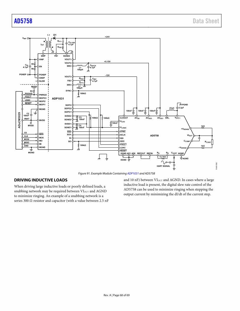
AD5758 Data Sheet
Rev. A | Page 68 of 69
Tx1
VINP
PGNDP
SW2
FB1VOUT1
VOUT2
SYNC
SW3
FB3
PGNDP
VINP
SLEW
PWRGD
SWP
L1100µH
VOUT3
CIN4.7µF
CFLYBK4.7µF
CBUCK4.7µF
CINVGNDP
MGND
SGND1
SGND2MVDD
MSSMCKMOMI
MGPO3
SSSSCK
SISO
SGPI3
MGPI2MGPI1
SGPO2SGPO1
MGND
PGOOD
VBAT
CSCLKMOSIMISO
FAULTLDACRESET
GND
SVDD1
EN
SVDD2
L2100µH
D11:1
RFT1
RFB1
C3100nF
C4100nF
RFB3
RFT3
R5
R6
ADP1031
SGND2
MVDD
C2100nF
MGND
MVDD
R3
AD
uCM
3029
REFIN
SDISDO
SCLK AD5758
CHART
VIOUT
SYNC
AVDD2 AVDD1 SW+AVSS
FAULT
HART SIGNAL
VLDO
VLOGIC
47µH 2.2µFPGND
REFOUTAD1 AD0
DGND13.7kΩ
RA RB
100nF
VDPC+
+VSENSE
–VSENSE
DGND AGND
AGND
RLOAD
1kΩ
1kΩLDAC
CLKOUT
RESET
CCOMP
100nF100nF
100kΩ100kΩ
100kΩ
100nF
+24V
+5.15V
–12V
4.7µF
100kΩ
1184
0-09
2
Figure 91. Example Module Containing ADP1031 and AD5758
DRIVING INDUCTIVE LOADS When driving large inductive loads or poorly defined loads, a snubbing network may be required between VIOUT and AGND to minimize ringing. An example of a snubbing network is a series 300 Ω resistor and capacitor (with a value between 2.5 nF
and 10 nF) between VIOUT and AGND. In cases where a large inductive load is present, the digital slew rate control of the AD5758 can be used to minimize ringing when stepping the output current by minimizing the dI/dt of the current step.
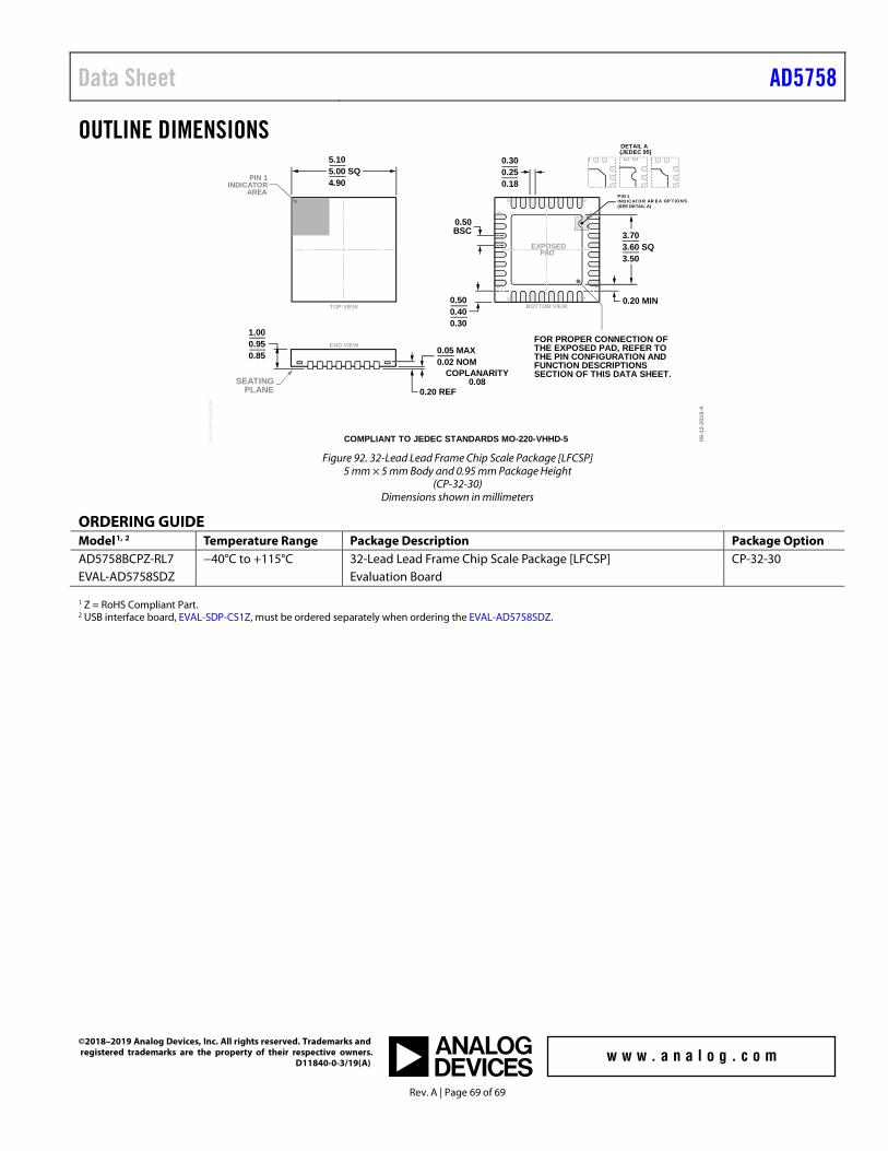
Data Sheet AD5758
Rev. A | Page 69 of 69
OUTLINE DIMENSIONS
1
0.50BSC
BOTTOM VIEWTOP VIEW
32
916
17
24
25
8
0.05 MAX0.02 NOM
0.20 REF
COPLANARITY0.08
0.300.250.18
5.105.00 SQ4.90
1.000.950.85
0.500.400.30
0.20 MIN
3.703.60 SQ3.50
09-1
2-20
18-A
COMPLIANT TO JEDEC STANDARDS MO-220-VHHD-5PKG
-004
754/
0052
09
EXPOSEDPAD
END VIEW
PIN 1IN D ICATO R AR E A OP TIO N S(SEE DETAIL A)
DETAIL A(JEDEC 95)
FOR PROPER CONNECTION OFTHE EXPOSED PAD, REFER TOTHE PIN CONFIGURATION ANDFUNCTION DESCRIPTIONSSECTION OF THIS DATA SHEET.
SEATINGPLANE
PIN 1INDICATOR
AREA
Figure 92. 32-Lead Lead Frame Chip Scale Package [LFCSP]
5 mm × 5 mm Body and 0.95 mm Package Height (CP-32-30)
Dimensions shown in millimeters
ORDERING GUIDE Model1, 2 Temperature Range Package Description Package Option AD5758BCPZ-RL7 −40°C to +115°C 32-Lead Lead Frame Chip Scale Package [LFCSP] CP-32-30 EVAL-AD5758SDZ Evaluation Board 1 Z = RoHS Compliant Part. 2 USB interface board, EVAL-SDP-CS1Z, must be ordered separately when ordering the EVAL-AD5758SDZ.
©2018–2019 Analog Devices, Inc. All rights reserved. Trademarks and registered trademarks are the property of their respective owners. D11840-0-3/19(A)
Top Related