


Languages
Pages
Legal

60 GHz Tapered Transmission Line Resonators
Cristian MarcuAli Niknejad
Electrical Engineering and Computer SciencesUniversity of California at Berkeley
Technical Report No. UCB/EECS-2008-117
http://www.eecs.berkeley.edu/Pubs/TechRpts/2008/EECS-2008-117.html
September 15, 2008

Copyright 2008, by the author(s).All rights reserved.
Permission to make digital or hard copies of all or part of this work forpersonal or classroom use is granted without fee provided that copies arenot made or distributed for profit or commercial advantage and that copiesbear this notice and the full citation on the first page. To copy otherwise, torepublish, to post on servers or to redistribute to lists, requires prior specificpermission.
Acknowledgement
The authors would like to thank the BWRC sponsors, NSF InfrastructureGrant No. 0403427, wafer fabrication donation by STMicroelectronics,DARPA TEAM program (contract no. DAAB07-02-1-L428), Motorola, andthe UC-Micro program.

60 GHz Tapered Transmission Line Resonators
by Cristian Marcu
Research Project
Submitted to the Department of Electrical Engineering and Computer Sciences, University of California at Berkeley, in partial satisfaction of the requirements for the degree of Master of Science, Plan II. Approval for the Report and Comprehensive Examination:
Committee:
Professor Ali M. Niknejad Research Advisor
(Date)
* * * * * * *
Professor Elad Alon Second Reader
(Date)


i
Contents
List of Figures ii
List of Tables iv
1 Introduction 1
2 Tapered Transmission Line Resonators 72.1 Tapering Principle . . . . . . . . . . . . . . . . . . . . . . . . . . . . . . . . 72.2 Transmission Line Equations . . . . . . . . . . . . . . . . . . . . . . . . . . 92.3 Taper Optimization . . . . . . . . . . . . . . . . . . . . . . . . . . . . . . . 11
2.3.1 EM Model Extraction . . . . . . . . . . . . . . . . . . . . . . . . . . 122.3.2 Optimization Methodology . . . . . . . . . . . . . . . . . . . . . . . 172.3.3 Optimization Results . . . . . . . . . . . . . . . . . . . . . . . . . . . 20
2.4 Experimental Results . . . . . . . . . . . . . . . . . . . . . . . . . . . . . . . 222.4.1 Accounting for Deembedding Inaccuracies . . . . . . . . . . . . . . . 27
2.5 Comparison to lumped LC tank . . . . . . . . . . . . . . . . . . . . . . . . . 30
3 Conclusion 33
Bibliography 36

ii
List of Figures
1.1 Cross-coupled differential pair VCOs with LC tank (left) and quarter wave-length transmission line resonators (right). . . . . . . . . . . . . . . . . . . . 3
2.1 The current and voltage standing wave ratio on a lossless quarter wave trans-mission line. . . . . . . . . . . . . . . . . . . . . . . . . . . . . . . . . . . . . 8
2.2 A tapered quarter wave transmission line utilizes wide width and large gapspacing when the current is high (voltage is low) and narrow width and smallgap when the voltage is high (current is low). . . . . . . . . . . . . . . . . . 8
2.3 RLGC ladder representation of a transmission line. . . . . . . . . . . . . . . 92.4 Uniform shorted differential stripline. . . . . . . . . . . . . . . . . . . . . . . 122.5 Characteristic impedance of differential stripline. . . . . . . . . . . . . . . . 132.6 RLGC per meter for a uniform differential stripline. . . . . . . . . . . . . . 152.7 Resonant Q of quarter wavelength uniform differential stripline. . . . . . . . 172.8 Tapered resonator optimization flow chart. . . . . . . . . . . . . . . . . . . . 192.9 The layout of the optimized quarter wave line. The characteristic impedance
Z0 is non-constant. Slotting is introduced to satisfy design rules. . . . . . . 202.10 The optimum characteristic impedance Z0 profile. . . . . . . . . . . . . . . 202.11 The layout of the optimized capacitor loaded half-resonator. The character-
istic impedance Z0 is non-constant. Slotting is introduced to satisfy designrules. . . . . . . . . . . . . . . . . . . . . . . . . . . . . . . . . . . . . . . . . 21
2.12 Layout of resonator test structures. . . . . . . . . . . . . . . . . . . . . . . . 232.13 Layout of deembedding structure. . . . . . . . . . . . . . . . . . . . . . . . . 242.14 Measured and simulated impedance for the uniform resonator. . . . . . . . 252.15 Measured and simulated impedance for the tapered resonator. . . . . . . . . 262.16 Measured and simulated impedance for the capacitor-loaded tapered half-
resonator. (Capacitor Q is assumed to be 40 in simulation.) . . . . . . . . . 262.17 Tapered resonator 3D layout model in HFSS including undeembedded inter-
connect and microstrip to CPS transition. The two insets show the actualextent of deembedding (left) compared to the expected deembedding (right). 28
2.18 Measured and simulated impedance for the tapered resonator taking intoaccount the deembedding structure layout error. . . . . . . . . . . . . . . . 29
2.19 Single turn octagonal inductor layout in HFSS using only the top metal layer. 31

iii
2.20 Simple inductor model taking into account series losses. . . . . . . . . . . . 312.21 Inductive Q versus inductance comparison between standard single turn oc-
tagonal inductors and tapered half-resonator. . . . . . . . . . . . . . . . . . 32
3.1 A tapered open ended half wave transmission line utilizes wide width andlarge gap spacing when the current is high (voltage is low) and narrow widthand small gap when the voltage is high (current is low). . . . . . . . . . . . 34

iv
List of Tables
2.1 Measurement Results . . . . . . . . . . . . . . . . . . . . . . . . . . . . . . . 26

v
Acknowledgments
The authors would like to thank the BWRC sponsors, NSF Infrastructure Grant No.
0403427, wafer fabrication donation by STMicroelectronics, DARPA TEAM program (con-
tract no. DAAB07-02-1-L428), Motorola, and the UC-Micro program.

1
Chapter 1
Introduction
Millimeter-wave transceivers require a local reference frequency for upconversion
from baseband to RF for transmission, or downconversion of received RF signals down
to baseband. This reference can also be divided down to a lower frequency for use as
the baseband clock signal. Voltage controlled oscillators (VCOs) can provide this local
frequency reference either as free-running oscillators or locked to a stable reference using
phase locked loops. Typically, VCOs which utilize a resonant tank achieve the best overall
performance, and thus are very common in mm-wave applications. The design of CMOS
mm-wave VCOs, however, involves a complex set of trade-offs between tuning range, phase
noise, DC power consumption, and output power. In many cases, the most important of
these metrics are tuning range and phase noise. The tuning range of the VCO must be
large enough to cover the desired band of interest taking into account process, voltage,
and temperature variations as well as modelling inaccuracies. Phase noise, on the other
hand, contributes to the overall noise figure of the transceiver by causing downconversion of

2
noise and any undesired signals located in frequencies adjacent to the desired signal. Both
metrics, however, are strongly dependent on the type and quality factor of the resonant
tank used, as shown by Leeson’s well known equation for the phase noise of an oscillator [1].
L∆ω = 10log
[S(∆ω)
1 +
ω0
2Q∆ω
](1.1)
Even though this equation is based on an LTI approximation, it gives valuable insight into
the design parameters. For example, we can see that in order to minimize oscillator phase
noise, a high Q resonant tank must be used.
The most common tank is simply a parallel LC tank. Usually the tank inductance
is kept constant since it is very difficult to tune an inductor, and the tuning comes from
changing the capacitance value. This can be accomplished either by switching in and out
small capacitors, using varactors for part of the capacitance, or both. However, at high
frequencies the size of these lumped components begins to approach an appreciable fraction
of the wavelength, and thus these lumped components begin to exhibit distributed behavior.
Transmission lines are a necessary component of high frequency and mm-wave
designs because they explicitly take into account this distributed behavior. They can be
used not only to carry signals, but also as reactive components and resonators. This work
focuses on their use as resonators for 60 GHz CMOS applications and seeks to achieve
higher resonant quality factors than what is achievable with lumped components.
A quarter-wavelength of transmission line shorted at one end looks like an open
circuit from the opposite end and thus behaves like a parallel LC tank. By applying a
negative resistance, such as a cross-coupled differential pair, this transmission line can be
used to create an oscillator as shown in Fig. 1.1. A signal travels from the negative resistance

3
Vdd
bias
out+out-
Vdd
bias
out+out-
Figure 1.1: Cross-coupled differential pair VCOs with LC tank (left) and quarter wavelengthtransmission line resonators (right).
cell to the shorted end of the line where it is reflected and travels back to the source. The
sum of these two travelling waves forms a standing wave pattern along the transmission
line. It is this standing wave behavior of such an oscillator which can be exploited to lower
losses along the line through the use of tapering.
The idea of tapering a transmission line has been studied and used extensively
in the microwave community for many years as a way to provide a conjugate match be-
tween two sections of transmission line with different characteristic impedances. Initially
this work began as a cascade of quarter-wavelength sections of transmission line with differ-
ent characteristic impedances, also known as quarter-wavelength transformers due to their
impedance transformation characteristics, and evolved into single tapered sections of line.
As early as the 1930s many authors had worked out solutions for the behavior of a tapered
4
transmission line with characteristic impedance profiles that varied in a specified manner
(ie: exponential, Gaussian, etc.). However, Collin, [2] was the first to produce an analysis
of what constitutes an optimum taper and the synthesis of such a taper. The results of
this work showed that the optimal synthesis described obtained better performance than
comparable exponential or Gaussian tapers.
Recently, the idea of tapering has resurged in microwave integrated circuits. Due
to the presence of lossy substrates and the expense associated with RF process options such
as thick top metal layers far away from the substrate, CMOS designers have a very hard
time designing high quality factor inductors for mm-wave VCOs. However, at such high
frequencies it becomes possible to use on-chip transmission lines which utilize a reasonable
amount of area. The most popular forms of integrated transmission lines have been mi-
crostrip, coplanar waveguide (CPW), and coplanar stripline (CPS). Microstrip lines offer
great flexibility in layout and effectively shield the signals from the lossy substrate. How-
ever, the ground plane must be placed in a thin, low metal layer, thus increasing the loss.
This is due to the fact that the characteristic impedance is mainly detemined by the ratio of
signal width to the distance between signal and ground. Thus, the ground and signal must
be placed as far apart as possible to allow the use of wide signal lines. Coplanar waveguides
have both the signal and ground lines in the topmost thick metal layer and thus tend to
provide lower loss for small spacings. The characteristic impedance is determined by both
the signal width and the spacing between the signal and ground lines, however, it is most
sensitive to the spacing. Unfortunately, as the spacing is increased, more fields penetrate
the substrate and thus the loss increases. The coplanar stripline is similar to a coplanar
5
waveguide in that both signals are in the topmost thick metal layer and suffer from the
same spacing limitation. However, the coplanar stripline is inherently a differential struc-
ture and thus lends itself very well to the design of quarter wavelength resonators for VCOs.
Moreover, the differential characteristic impedance has a similar dependence on both the
width of the signal lines and their spacing.
Andress first proposed the idea of tapering a differential CPS transmission line
resonator to reduce its loss and thus enhance its quality factor [3]. The characteristic
impedance was kept constant to eliminate internal reflections and simplify the synthesis of
an optimal taper. Similarly, Krishnaswamy utilized a CPS transmission line with shielding
to create a very high quality factor inductor [4]. Due to the large spacing required to get the
necessary inductance, the author devised an optimal taper to interface to the much smaller
active cell of the VCO core.
This work builds on [3] by removing the constraint on characteristic impedance.
If the characteristic impedance of the line is kept constant along its length, the voltage
and current waveforms in the phase domain are sinusoidal in shape regardless of the shape
of the line, allowing a relatively straightforward optimization. However, this approach is
theoretically limited to a 60% improvement in quality factor Q over the uniform resonator.
By removing the constraint on the characteristic impedance, this work achieves further
improvements in Q, limited only by the substrate losses. Determining the optimum taper
shape is however a complex multi-dimensional optimization problem made more difficult
by the fact that the characteristic impedance profile can vary arbitrarily. Thus, the voltage
and current waveforms cannot be derived analytically and a numerical approach must be

6
used in the optimization.
The optimization results in a resonator with very narrow width for much of its
length. In a usual VCO implementation like the one shown in Fig. 1.1, the resonator would
be used to bias up the VCO core and would thus need to carry DC current. With this in
mind, the narrow section can be removed and replaced with a capacitor. In this way, the
shorted length of transmission line is being used as an inductor as in [4]. This tapered,
capacitor-loaded half-resonator can exhibit higher quality factor than the full resonator de-
pending on the quality of the lumped capacitor used and still maintains the optimal behavior
of the full taper. As a final note, this work explores the benefits that this optimization can
provide as a function of frequency, leading to a conclusion on its possible applications.

7
Chapter 2
Tapered Transmission Line
Resonators
2.1 Tapering Principle
A differential stripline shorted at one end exhibits the standing wave mode shown
in Fig. 2.1 at resonance. At the shorted end of the line, the voltage is at a minimum and the
current at a maximum, so the losses at this point come mainly from the series resistance of
the metal line. Conversely, at the driven end, the voltage is at a maximum and the current
at a minimum, so the losses at this point come mainly from the shunt conductance between
the differential lines. This phenomenon can be exploited to lower the losses of the resonator
and thus raise the quality factor [3]. At the shorted end of the line, the metal conductors can
be made wider to reduce the series resistance without having to worry about the increase
in shunt conductance. The gap spacing can also be made wide since the voltage difference

8
-1 -0.8 -0.6 -0.4 -0.2 0 0
0.5
1
1.5
2
Normalized Position
VoltageCurrent
Figure 2.1: The current and voltage standing wave ratio on a lossless quarter wave trans-mission line.
between the lines is small. Similarly, at the driven end of the line, the conductors can be
made very narrow to lower the conductance without having to worry about the increase in
series resistance. The gap spacing should be small in order to minimize field leakage into
the substrate since the fields are strongest at this end of the line. Along the rest of the line,
shunt conductance and series resistance can be traded off to achieve a tapered line with
Figure 2.2: A tapered quarter wave transmission line utilizes wide width and large gapspacing when the current is high (voltage is low) and narrow width and small gap when thevoltage is high (current is low).
9
L
C
R
G
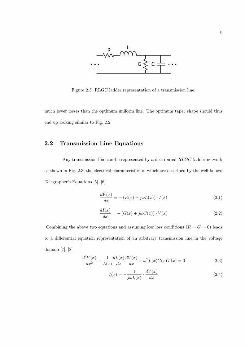
Figure 2.3: RLGC ladder representation of a transmission line.
much lower losses than the optimum uniform line. The optimum taper shape should thus
end up looking similar to Fig. 2.2.
2.2 Transmission Line Equations
Any transmission line can be represented by a distributed RLGC ladder network
as shown in Fig. 2.3, the electrical characteristics of which are described by the well known
Telegrapher’s Equations [5], [6].
dV (x)dx
= − (R(x) + jωL(x)) · I(x) (2.1)
dI(x)dx
= − (G(x) + jωC(x)) · V (x) (2.2)
Combining the above two equations and assuming low loss conditions (R = G = 0) leads
to a differential equation representation of an arbitrary transmission line in the voltage
domain [7], [8]
d2V (x)dx2
− 1L(x)
dL(x)dx
dV (x)dx
− ω2L(x)C(x)V (x) = 0 (2.3)
I(x) = − 1jωL(x)
· dV (x)dx
(2.4)

10
or in the current domain
d2I(x)dx2
− 1C(x)
dC(x)dx
dI(x)dx
− ω2L(x) · C(x) · I(x) = 0 (2.5)
V (x) = − 1jωC(x)
· dI(x)dx
(2.6)
Previous work [3] has shown that the transforms defined in Eq. 2.7 and Eq. 2.8
Lθ(θ) =L(x)β(x)
=L(x)
ω√
L(x)C(x)=
1ω
√L(x)C(x)
=Z0(x)
ω(2.7)
Cθ(θ) =C(x)β(x)
=C(x)
ω√
L(x)C(x)=
1ω
√C(x)L(x)
=1
ωZ0(x)(2.8)
can be used to convert the transmission line equations presented above from the physical
domain to the phase domain described by
θ(x) =∫ x
0β(x′)dx′ =
∫ x
0ω
√L(x′)C(x′)dx′ (2.9)
Under these transforms Eq. 2.3 becomes
d2V (θ)dθ2
− 1Z0(θ)
dZ0(θ)dθ
dV (θ)dθ
− V (θ) = 0 (2.10)
whose solution can be found analytically if the characteristic impedance profile is well
behaved (ie.: constant [3], linear [9], exponential [8], etc.). For example, if the characteristic
impedance is kept constant, the second term in Eq. 2.10 goes to zero and the dependence
of the voltage profile on characteristic impedance, and thus on the shape of the taper,
completely drops out leading to Eq. 2.11.
d2V (θ)dθ2
− V (θ) = 0 (2.11)
The solution to this differential equation is a sinusoid. However, if the characteristic
impedance is allowed to vary, as in this work, the voltage profile is a complex function

11
of the taper shape even in the phase domain. Therefore, from this point on we elect to
use Eqs. 2.3 and 2.4, the equations for voltage in the physical domain, since working in the
phase domain provides no advantages. Due to the fact that the characteristic impedance
profile is not known and can vary arbitrarily, Eqs. 2.3 and 2.4 are nonlinear and cannot
be solved analytically [8]. Instead, we turn to a numerical solution. A Matlab script was
developed to solve for the voltage and current waveforms along an arbitrary transmission
line for which the L(x) and C(x) profiles are known. This script numerically solves Eq. 2.3
and 2.4 with boundary conditions of V (0) = 1 and V ′(0) = 0. The resonant quality factor
can then be calculated by computing the ratio of energy stored to energy dissipated per
cycle using Eq. 2.12.
Q = ωEstored
Pdiss= ω
∫ `0
14
(V 2(x)C(x) + I2(x)L(x)
)dx∫ `
012 (V 2(x)G(x) + I2(x)R(x)) dx
(2.12)
2.3 Taper Optimization
The goal of this optimization is maximizing the resonant quality factor. Thus, we
can see from Eq. 2.12 that this means maximizing energy storage while minimizing energy
losses. The taper optimization is accomplished with the help of Momentum, a 2.5D EM
simulator, HFSS, a 3D EM simulator, and Matlab. Momentum and HFSS were first used
to extract RLGC models for differential strip lines of varying widths and spacings covering
the desired design space. The transmission line RLGC model was chosen over the Z0 and Γ
model since it provides more intuition for this particular optimization. It is relatively easy
to explain changes in resistance, inductance, conductance, and capacitance based on layout
changes as opposed to determining changes in Z0 or Γ. Furthermore, the optimization is

12
s
w
w
l
Figure 2.4: Uniform shorted differential stripline.
based exactly on understanding how layout changes affect energy losses, due to resistance
and conductance, and energy storage, due to inductance and capacitance. Matlab was used
to actually run the optimizations and, finally, HFSS and Momentum were used to simulate
the resulting taper shape to verify the optimization results.
2.3.1 EM Model Extraction
Momentum, which is a 2.5D EM simulator, was chosen for EM model extraction
due to its speed when simulating simple structures. The technology used for the transmis-
sion line implementation is a standard digital 90nm CMOS process in which we used the
top metal layer. The planar nature of this process allows us to use Momentum with little or
no loss of accuracy when compared to a full 3D simulator such as HFSS. However, the full
substrate stack is made up of many oxide layers with different EM characteristics. To speed
up simulation time it is imperative to simplify the substrate stackup dramatically. This was
achieved by using only one oxide layer which encompasses all metal layers. The character-
istics of this oxide layer and the silicon substrate below were matched to measurements of
CPW transmission lines with varying widths and spacings.

13
010
2030
4050
010
2030
4050
0
50
100
150
200
250
300
|Z0|
s (µm) w (µm)
Figure 2.5: Characteristic impedance of differential stripline.
The simulation setup used a length of CPS transmission line, similar to the one
shown in Fig. 2.4, with variable conductor width, spacing, and length but without one end
shorted. One port was placed on either end of each conductor for a total of four ports which
were then configured into two differential ports, one for each side. Simulation results thus
provide a set of differential 2-port S-parameters for the given length of transmission line.
Over a wide frequency range, the RLGC parameters are frequency dependent, however, over
a narrow frequency range we can assume they are relatively constant. The optimization
seeks to find an optimum resonator only at 60 Ghz so that the calculations can be limited
to a narrow bandwidth and we can safely assume constant RLGC parameters. Thus, we
only need to simulate the S-parameters at one frequency point and extract the line’s RLCG
parameters from that point alone. This conversion is performed in multiple steps. First,
14
the S-parameters must be converted into ABCD parameters using Eq. 2.13-2.16.
A =(1 + S11)(1 − S22) + S12S21
2S21(2.13)
B = Z0(1 + S11)(1 + S22) − S12S21
2S21(2.14)
C =1Z0
(1 − S11)(1 − S22) − S12S21
2S21(2.15)
D =(1 − S11)(1 + S22) + S12S21
2S21(2.16)
Next, Z0 and Γ are computed from the ABCD parameters using Eq. 2.17 and Eq. 2.18.
Z0 =
√B
C(2.17)
Γ =arccosh(A)
l(2.18)
The resulting |Z0,diff | profile over the design space is shown in Fig. 2.5. The contours
show that the characteristic impedance of a differential CPS transmission line is strongly
dependent on width when the spacing is large but only weakly dependent on width when
the spacing is small. Finally, the RLGC parameters can be extracted from Z0 and Γ using
Eq. 2.19-2.22.
R = <(Z0Γ) (2.19)
L ==(Z0Γ)
ω(2.20)
G = <(ΓZ0
) (2.21)
C ==( Γ
Z0)
ω(2.22)
This process can be repeated for every combination of spacing and width within the design
space although this is not strictly necessary as results can be interpolated very accurately
between simulated points if the gradient in the region is small. The bounds of the design
15
010
2030
4050
010
2030
4050
0
20
40
60
80
w (µm)s (µm)
R (kΩ
/m)
010
2030
4050
010
2030
4050
0
0.5
1
1.5
2
w (µm)s (µm)
L (µ
H/m
)
010
2030
4050
010
2030
4050
0
5
10
15
w (µm)s (µm)
G (S
/m)
010
2030
4050
010
2030
4050
0
50
100
150
w (µm)s (µm)
C (p
F/m
)
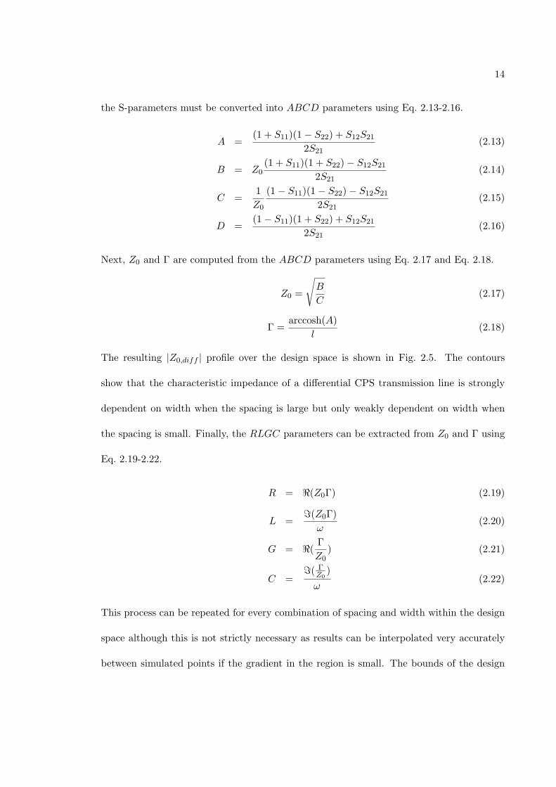
Figure 2.6: RLGC per meter for a uniform differential stripline.
space are determined by the maximum width and spacing required in the final tapered
resonator. Since this was not known a priori, a choice of 50µm was made for the maximum
width and spacing. As will be shown by the optimization results in section 2.3.3, this choice
proved to be satisfactory. The RLCG parameters for the differential stripline over the
design space are shown in Fig. 2.6.
Even before the actual optimization we can see from Fig. 2.6 that some of our
earlier intuition makes physical sense. The series resistance is stronly dependent on the

16
conductor width and only weakly dependent on the spacing. As the conductor becomes
wider, the series resistance initially drops very rapidly but then settles to an almost constant
value. This is because skin effect at these frequencies limits the minimum resistance that can
be achieved and the differential operation of the transmission line creates current crowding
along the inner edges meaning little or no current flows on the outer edges. Thus, as the
conductor is made wider extra metal is added where no current is flowing so the effective
resistance is not actually changed. Conductor spacing only affects the series resistance
when the conductors are very close together due to proximity effects which increase current
crowding on the inner edges. This raises the effective series resistance. As the conductors
are pulled apart this effect diminishes very rapidly, becoming insignificant.
The shunt conductance is also strongly dependent on the conductor width. Wider
metals lead to more capacitive coupling to the conductive substrate which in turn increases
the shunt conductance between the differential lines. Inductance is mainly determined by
the spacing of the lines, or put another way, the enclosed loop area. Shunt capacitance is
dominated by the parallel plate capacitance between the metal lines when they are close
together and fringing capacitance when they are far apart. As the metal is made wider,
fringing capacitance increases, raising the overall shunt capacitance.
As a final note, the transmission line length, l, is kept the same for each simulation
for simplicity but this does not affect the results since Γ is normalized before computing the
RLGC parameters. The choice of the actual length, however, is governed by the frequency
of interest. A short line may not provide accurate results if the correct transmission line
mode cannot be established in the simulation. A long line, on the other hand, may give

17
010
2030
4050
0
10
20
30
40
500
2
4
6
8
10
Reso
nant
Q
s (µm) w (µm)
Figure 2.7: Resonant Q of quarter wavelength uniform differential stripline.
incorrect results if its length is close to an integer multiple of half the wavelength at the
frequency of interest. This is because the simulation setup is that of an open ended stub
which exhibits a parallel resonance mode when its length is equal to an integer multiple
of half the wavelength. The mathematical equations used to extract RLGC models in
Eq. 2.13-2.22 become innacurate near the frequency at which this occurs since the numbers
involved can become very large or very small. Thus, it is prudent to maintain a length less
than half a wavelength to avoid resonance effects, but at least one fifth the wavelength to
ensure a transmission line mode is established in the simulation.
2.3.2 Optimization Methodology
The first step in the optimization is to find the optimum uniform resonator as
a reference. The resonant Q of a shorted quarter wavelength uniform transmission line

18
resonator can be found using Eq. 2.23 and the values of Γ computed earlier during the
RLGC model extraction.
Q =β
2α=
=(Γ)2<(Γ)
(2.23)
The result of this computation for all the points in the design space is shown in Fig. 2.7.
Thus, finding the optimum uniform resonator is as easy as finding the maximum of Fig. 2.7.
In this case the optimum width and spacing are both 5 µm and the resulting Q is approxi-
mately 9.5. This is in line with measured data of transmission lines in this process and will
be the reference Q for the optimization to follow.
The uniform resonator is first split up by choosing a number of equally spaced
vertices along its horizontal length which are used to set the width and spacing at those
positions. At every other point the width and spacing are interpolated from the known
values at the vertices. The optimization variables are thus the width and spacing values
at each vertex and the overall resonator length which is used as a scaling factor for the
horizontal vertex positions. This is necessary because β will not be constant over the length
of the tapered resonator and thus the quarter wavelength at 60 GHz will vary as the tapering
is varied. The initial values for all vertices are set to the optimal width and spacing for a
uniform resonator and the length is set to the nominal quarter wavelength at 60 GHz.
To find the optimum tapered resonator, all optimization variables are jointly op-
timized. This requires an iterative approach whereby the voltage and current profiles along
a given taper shape are first found by numerically solving Eqs. 2.3 and 2.4, followed by an
optimization of the shape to those particular voltage and current standing waves with the
goal of maximizing Eq. 2.12. The distortion of the taper shape changes the voltage and

19
Load EM Simulation Data
Find S and W fora uniform TLinewith maximum Q
Solve VoltageCurrent DistributionAlong Uniform Line
Optimize Line ShapeFor the Given VoltageCurrent Distributions
Solve VoltageCurrent Distribution
Along Nonuniform Line
EM SimData
Is % change inS and W less than
Threshold?
Store LastS and W(vectors)
Optimize Line ShapeFor the Given VoltageCurrent Distributions
Optimum Taper AchievedOutput S and W
NO
YES
Figure 2.8: Tapered resonator optimization flow chart.
current profiles so they must be recomputed once the optimum shape has been found. The
taper shape is then optimized to the new voltage and current standing waves. This pro-
cess continues iteratively until the taper shape converges to an optimum. Random starting
points are utilized and multiple runs are averaged to increase the probability of reaching
a globally optimal shape. A flow chart of the entire process can be seen in Fig. 2.8. It
must be noted, however, that all of the above calculations assume that a perfect short
(R = 0, L = 0) is present at the end of the resonator. In the actual implementation a real
short would have nonzero resistance and inductance and will change the results somewhat.
It is expected that the center frequency of the resonator will be shifted down in frequency
due to the additional unnacounted series inductance.

20
498 µm
105 µ
m
Figure 2.9: The layout of the optimized quarter wave line. The characteristic impedanceZ0 is non-constant. Slotting is introduced to satisfy design rules.
0 50 100 150 200 250 300 350 400 45060
70
80
90
100
110
120
130
140
150
160
Position (µm)
Di
eren
tial Z
0 (Ω
)
Figure 2.10: The optimum characteristic impedance Z0 profile.
2.3.3 Optimization Results
The optimum shape derived by the method described in section 2.3.2 is shown in
Fig. 2.9 and has the characteristic impedance profile shown in Fig. 2.10. According to the
Matlab calculations this shape should have a quality factor of just over 15, an improvement
of more than 60% compared to the uniform resonator. As mentioned in section 2.3.2, the
optimization averaged multiple runs with random starting points to arrive at this optimal
shape. Most of the results were nearly identical in shape and quality factor, while the outliers
achieved significantly lower quality factors and were thus eliminated before averaging.

21
274 µm
105 µ
m
Figure 2.11: The layout of the optimized capacitor loaded half-resonator. The characteristicimpedance Z0 is non-constant. Slotting is introduced to satisfy design rules.
Interestingly, the resulting characteristic impedance is not constant, but varies
widely over the length of the resonator. The sharp step in characteristic impedance shows
that the transmission line is more capacitive for the left half where most of the energy is
stored in the electric field than the right half where most of the energy is stored in the
magnetic field. This is clearly reminiscent of an LC tank with the left half of the resonator
representing a distributed capacitor and the right half, a loop inductor. This step is also
the point where the dominant losses change from resistive to conductive. Unfortunately,
this result presents a problem for implementation into a VCO where the resonant tank is
usually used to bias the VCO core and thus must carry a DC current. The very narrow
metal widths present in the left half of this resonator would cause a large DC voltage drop.
However, we can take advantage of the realisation that the left half of the resonator is
essentially just a distributed capacitor which can be replaced by a lumped capacitor. The
equivalent capacitance can be found by integrating C(x) over the left-half of the resonator
as shown in Eq. 2.24.
Ceff =∫ −L
2
−LC(x′)dx′ (2.24)

22
Replacing the left half of the resonator with a lumped capacitor also reduces the area oc-
cupied by the resonator and, depending on the quality of the capacitor, can reduce overall
losses leading to higher resonator Q. Conceptually, this is shown in Fig. 2.11. Due to the
availability of MIM capacitors in our process we chose this type for the actual implementa-
tion due to their high quality factor and capacitance density.
To verify the Matlab computations, HFSS was used to simulate all three versions
of transmission line resonator: uniform, tapered, and half-taper. The shorted half resonator
by itself simply acts like an inductor so its simulation results are placed in parallel with
a capacitor with a Q of 40 at 60 GHz and a capacitance computed using Eq. 2.24. These
results will be shown alongside measurements for comparison in section 2.4.
2.4 Experimental Results
All three resonator versions were fabricated in a standard 90nm digital CMOS
process with no RF options. The transmission line resonators shown in Figures 2.9 and
2.11 are shown without the interface that would be required to connect them to the VCO
core. In most cases this interface would involve vias down to lower metal layers and routing
leading to the actual transistors in the VCO core. This interface must always be taken into
account in the design but in the case of characterizing the resonator alone we must interface
it to an appropriate pad structure. In this case, due to the lack of high frequency differential
pads, the measurement had to be done with two single ended ground-signal-ground (GSG)
pads. Due to physical limitations on the probe station the pads had to be positioned
directly opposing each other. Unfortunately, each pad layout has a built in section of 50Ω
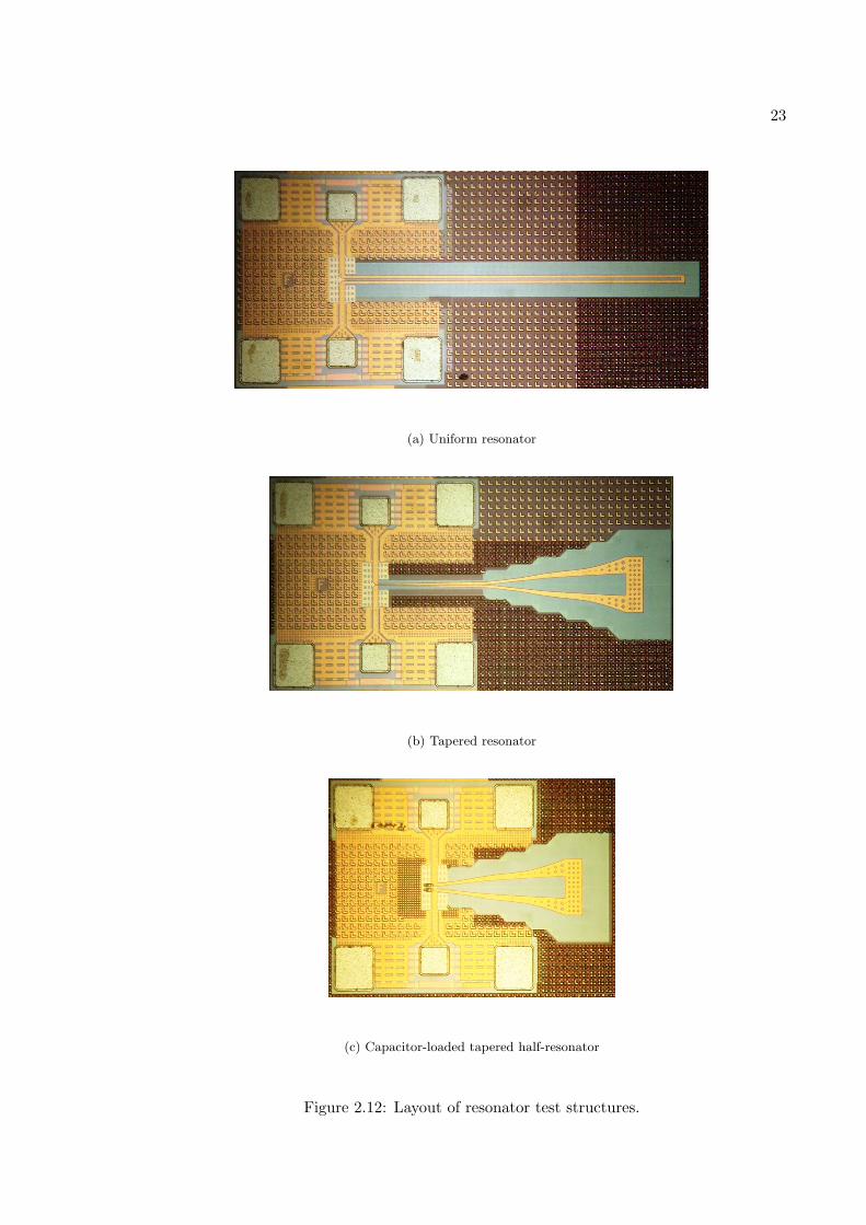
23
(a) Uniform resonator
(b) Tapered resonator
(c) Capacitor-loaded tapered half-resonator
Figure 2.12: Layout of resonator test structures.
24
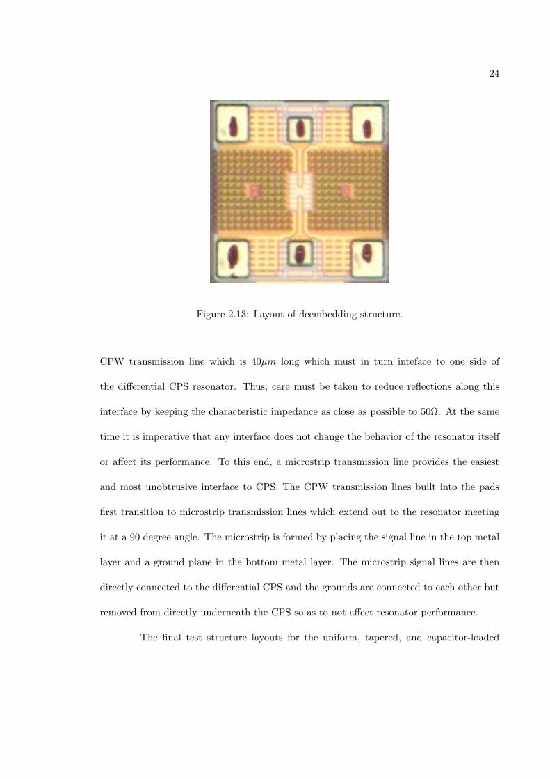
Figure 2.13: Layout of deembedding structure.
CPW transmission line which is 40µm long which must in turn inteface to one side of
the differential CPS resonator. Thus, care must be taken to reduce reflections along this
interface by keeping the characteristic impedance as close as possible to 50Ω. At the same
time it is imperative that any interface does not change the behavior of the resonator itself
or affect its performance. To this end, a microstrip transmission line provides the easiest
and most unobtrusive interface to CPS. The CPW transmission lines built into the pads
first transition to microstrip transmission lines which extend out to the resonator meeting
it at a 90 degree angle. The microstrip is formed by placing the signal line in the top metal
layer and a ground plane in the bottom metal layer. The microstrip signal lines are then
directly connected to the differential CPS and the grounds are connected to each other but
removed from directly underneath the CPS so as to not affect resonator performance.
The final test structure layouts for the uniform, tapered, and capacitor-loaded

25
40 45 50 55 60 65 70 75 8040
45
50
55
60
65
Frequency (GHz)
Tank
Impe
danc
e (d
B)
simmeas
BW: 6.4 GHz
Figure 2.14: Measured and simulated impedance for the uniform resonator.
tapered half-resonators are shown in Figures 2.12(a), 2.12(b), and 2.12(c) respectively. An
open-short deembedding procedure is used to remove the effects of the pads, CPW and
microstrip transmission lines, and all associated transitions. The layout of a deembedding
structure used for this procedure is shown in Fig. 2.13. This layout has to include the pads
and microstrip transmission lines in an identical configuration to that used in the resonator
test structures. For the open deembedding structure the microstrip signal lines are left
floating, while for the short deembedding structure vias are placed to connect the signal
lines to the ground plane below.
Figures 2.14, 2.15, and 2.16 show the measured and simulated absolute value of
impedance versus frequency for the uniform, tapered, and capacitor-loaded resonators re-
spectively. A systematic offset of approximately 4 GHz is present for all resonator versions,
due to deembedding inaccuracies and some process variations which will be explained in
section 2.4.1. However, the quality factor is consistent with simulation. Table 2.1 summa-

26
40 45 50 55 60 65 70 75 8040
45
50
55
60
65
Frequency (GHz)
Tank
Impe
danc
e (d
B)
simmeasBW: 3.5 GHz
Figure 2.15: Measured and simulated impedance for the tapered resonator.
40 45 50 55 60 65 70 75 8040
45
50
55
60
65
Frequency (GHz)
Tank
Impe
danc
e (d
B)
simmeas
BW: 3.5 GHz
Figure 2.16: Measured and simulated impedance for the capacitor-loaded tapered half-resonator. (Capacitor Q is assumed to be 40 in simulation.)
Resonator Type f0 (GHz) Q ∆Q
Uniform (ref.) 57.9 8.8 –Tapered 54.4 15 70.4%
Cap-Loaded Half-Taper 55.4 15.1 71.6%
Table 2.1: Measurement Results

27
rizes the measurement results for the three types of resonators. Interestingly, while both
versions of tapered resonators exhibited quality factors extremely close to those predicted
by Matlab simulations, the quality factor of the uniform resonator came out slightly lower
than expected.
Measurement results show a 70% improvement in Q over the uniform resonator
using our optimization, slightly better than predicted by Matlab computations. We believe
that the increased substrate losses present at 60 GHz prevent us from achieving further
improvements. However, using a lower loss substrate or operating at a lower frequency
could allow Q improvements of well over 100%. While a thicker metal option would not
necessarily help at our current frequency, due to skin effect, at lower frequencies the skin
effect would decrease and thicker metal options would certainly be advantageous.
2.4.1 Accounting for Deembedding Inaccuracies
As mentioned above in section 2.4, an open-short deembedding procedure was used
to remove the effects of pads, transmission lines and transitions leading up to the resonator.
This procedure requires the measurement of “open” and “short” deembedding structures.
These structures must be identical to the ones used in the resonator test structure except the
resonator itself is replaced with an open circuit and short circuit respectively. Unfortunately,
a layout error is present in the deembedding structures of the test chip used for this research
which caused a small portion of microstrip line to not be deembedded. As mentioned above
in section 2.4, the deembedding structures must be identical to the test structures in all
aspects while omitting only the actual device to be deembedded. In this case, however, the
microstrip transmission line in the deembedding structure was made shorter than in the

28
Figure 2.17: Tapered resonator 3D layout model in HFSS including undeembedded in-terconnect and microstrip to CPS transition. The two insets show the actual extent ofdeembedding (left) compared to the expected deembedding (right).

29
test structures and did not include the 45 taper of the microstrip to CPS transition which
can be seen in the test structure layouts in Fig. 2.12. In order to have a fair comparison
between measurement and simulation, this layout error must be taken into account in
simulation. Fig. 2.17 shows the HFSS 3D model of the tapered resonator including the
section of microstrip transmission line which was not deembedded. The inset on the right
hand side shows the expected deembedding down to the actual resonator, seen extending
out to the right. The left inset, on the other hand, shows the actual extent of deembedding
which left a portion of microstrip transmission line. Fig. 2.18 shows the absolue value of
impedance versus frequency comparing the measured value to the new HFSS simulation.
Clearly, the layout error accounts for most of the frequency offset seen in Figures 2.14, 2.15,
and 2.16.
40 45 50 55 60 65 70 75 8040
45
50
55
60
65
Frequency (GHz)
Tan
k Im
peda
nce
(dB
)
new simmeas
Figure 2.18: Measured and simulated impedance for the tapered resonator taking intoaccount the deembedding structure layout error.

30
2.5 Comparison to lumped LC tank
At low frequencies, distributed components such as the tapered resonator presented
here are simply too large to integrate on-chip since their size is on the order of the wavelength
at the frequency of interest, thus, leading to the use of lumped components. However, as
frequencies of operation scale higher, distributed components become a viable option since
the wavelength decreases. In this section we will determine whether or not it is beneficial to
use distributed over lumped components at 60 GHz in our 90nm digital CMOS process. The
tapered resonator can be directly compared to a lumped LC tank. As we saw in section 2.4,
replacing the distributed capacitance represented by the left half of the tapered resonator
with a high quality MIM capacitor had no effect on the overall resonator Q. The remaining
section of tapered resonator acts like an inductor so we can directly compare its inductive
quality factor to that of a lumped inductor in the same process. Standard, single turn,
octagonal inductors with various diameters and conductor widths were simulated in HFSS
using a single differential port accross the two terminals in the same method used for the
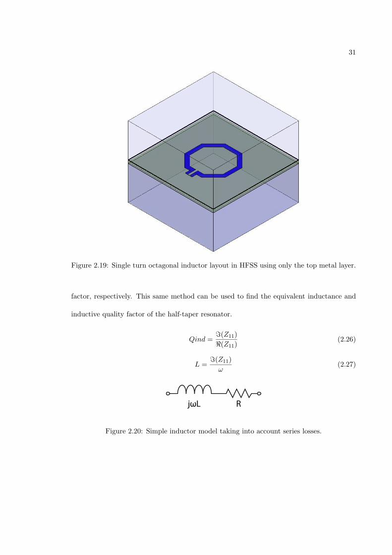
tapered resonators, and using the same substrate. A sample simulation setup is shown in
Fig. 2.19. For simplicity, we model the inductor as an resistor in series with an inductor
as shown in Fig. 2.20. In this way, the inductance and the quality factor can be easily
extracted from simulation using Z-parameters. The 1-port S-parameters from the HFSS
simulations are first converted to Z-parameters using Eq. 2.25.
Z11 = Z01 + S11
1 − S11(2.25)
Since this is a 1-port system, Z11 represents the impedance seen accross that port. Thus,
we can use Eqs. 2.26 and 2.27 to find the equivalent inductance and its inductive quality
31
Figure 2.19: Single turn octagonal inductor layout in HFSS using only the top metal layer.
factor, respectively. This same method can be used to find the equivalent inductance and
inductive quality factor of the half-taper resonator.
Qind ==(Z11)<(Z11)
(2.26)
L ==(Z11)
ω(2.27)
RjωL
Figure 2.20: Simple inductor model taking into account series losses.

32
0
5
10
15
20
25
30
100 200 300 400 500Inductance (pH)
Q
Width=5um Width=10umWidth=15um Tapered Half-Resonator
Figure 2.21: Inductive Q versus inductance comparison between standard single turn oc-tagonal inductors and tapered half-resonator.
To create a fair comparison, the quality factor was plotted versus the equivalent inductance
for each lumped inductor and for the half-taper resonator in Fig. 2.21. Unfortunately,
it seems that the tapered half-resonator is no better than an optimized, standard, single
turn octagonal lumped inductor. It is important to note that the diameters required in the
lumped inductor lead to a comparable but smaller overall area than the tapered transmission
line. These findings show that optimized inductors with MIM capacitors can perform as
well as optimized transmission line resonators at 60 GHz in our particular process while
occupying much less area.
33
Chapter 3
Conclusion
An optimum tapered transmission line resonator for 60 GHz applications was
presented using a differential stripline on a standard digital 90nm CMOS process with no
RF options. A comprehensive optimization approach was utilized to achieve the optimum
taper shape without any constraint on the characteristic impedance. The only constraints
on the design were due to design rules in our process which limited the minimum line
widths and spacings. This approach presents a transmission line resonator with a Q of 15,
an improvement of 70% over an optimum uniform resonator. This approach also has the
potential for much higher Q gains if lower loss substrates are available or at lower frequencies.
A capacitor-loaded tapered half-resonator was also developed and shown to have the same
Q improvement as its larger cousin while occupying much less area and reducing common
mode DC losses. This version would be very useful in the design of an integrated VCO
since it could be used to bias the VCO core without significant common mode DC voltage
drop. Another possible solution would be an open ended half wavelength resonator. This

34
Figure 3.1: A tapered open ended half wave transmission line utilizes wide width and largegap spacing when the current is high (voltage is low) and narrow width and small gap whenthe voltage is high (current is low).
arrangement is a trivial extension of this work since it can be seen as two quarter wavelength
resonators connected back to back as shown in Fig. 3.1. An additional advantage of this is
that an actual short between the two lines would not need to be provided since the horizontal
midpoint is a differential ground. The midpoint could be connected to the supply voltage to
bias up the VCO core but this interconnect could have a high inductance since it would not
have to also support signal currents. However, it was also shown that the tapered resonators
presented are currently no better than lumped components in quality factor yet consume
more area. At higher frequencies perhaps the balance will shift in favor of distributed
components. Nevertheless, it is possible that slow wave techniques could help improve the
quality factor of transmission line based resonators even at 60 GHz. This approach was
not explored during this research but work done in [4] shows that further improvements
could be possible with slow wave structures. Moreover, the use of such slow wave structures
would reduce the overall area occupied by the resonator and could make it comparable to,
or smaller than, the area of a lumped LC tank.
Other possible applications of this work include filters and transmission line match-
ing networks which utilize open and short shunt stubs. In filter applications transmission
line stubs would be used to replace LC tanks and would therefore be quarter or half wave-
35
length depending on the particular filter. Stubs used in matching networks, on the other
hand, are not necessarily a quarter or half wavelength since they must synthesize a different
impedance for each particular application. Nevertheless, the loss of these stubs adversly af-
fects the loss of the overall matching network. Therefore, the approach presented here could
be used to reduce the losses of matching transmission line stubs with some modifications.
Unlike resonators which look like parallel LC tanks, stubs must present a certain imaginary
impedance thus looking like either a capacitance, or an inductance. The optimization goal
would therefore need to be changed to take this into account. Instead of optimizing for
maximum resonant Q given a required center frequency, the goal would be to maximize
either capacitive or inductive Q, given a certain value of capacitance or inductance, respec-
tively. This approach has not been investigated in detail and would be a good topic for
further research.

36
Bibliography
[1] D.B. Leeson, “A Simple Model of Feedback Oscillator Noise Spectrum,” Proceedings of
the IEEE, vol. 54, pp. 329-330, 1966.
[2] R. E. Collin, “The Optimum Tapered Transmission Line Matching Section,” Proceedings
of the IRE, vol. 33, issue 4, pp. 539-548, Apr. 1956.
[3] W. F. Andress and D. Ham, “Standing Wave Oscillators Utilizing Wave-Adaptive Ta-
pered Transmission Lines,” IEEE J. Solid-State Circuits, vol. 40, no. 3, pp. 638-651,
Mar. 2005.
[4] H. Krishnaswamy, H. Hashemi, “A 26 GHz coplanar stripline-based current sharing
CMOS oscillator,” IEEE Radio Frequency Integrated Circuits Symposium 2005, Digest
of Papers, pp. 127-130, Jun. 2005.
[5] D. M. Pozar, Microwave Engineering, John Wiley & Sons, 2004.
[6] R. E. Collin, Foundations for Microwave Engineering, Wiley-IEEE Press, 2000.
[7] D. C. Youla, “Analysis and Synthesis of Arbitrarily Terminated Lossless Nonuniform

37
Lines,” IEEE Transactions on Circuits and Systems, vol. 11, issue 3, pp. 363-371, Sep.
1964.
[8] C. P. Womack, “The Use of Exponential Transmission Lines in Microwave Components,”
IRE Transactions on Microwave Theory and Techniques, vol. 10, issue, 2, pp. 124-132,
Mar. 1962.
[9] K. Lu, “An Efficient Method for Analysis of Arbitrary Nonuniform Transmission Lines,”
IEEE Transactions on Microwave Theory and Techniques, vol. 45, issue, 1, pp. 9-14, Jan.
1997.
Top Related