


Languages
Pages
Legal


2x2 module & stave layouts

2 options
• “Small chip”• “Big chip”• Boundary between “small” and “big” is determined by the
6” sensor wafer layout that must be compatible with bump bonding (will become clear later)
• “Small” chip has also a more natural number of rows & columns, but this is probably a minor issue for chip design.

Parameters
# cols total
# rows total
# ganged rows
# long cols
Long col width
Small chip 64 324 0 0 0
Small 2x2 tile 128 654 6 4 450um
Small active edge
1x1 tile
64 324 0 2 450um
big chip 70 348 0 0 0
big 2x2 tile 140 702 6 4 450um
big active edge
1x1 tile
70 348 0 2 450um
Normal col. width x row height = 250um x 50um
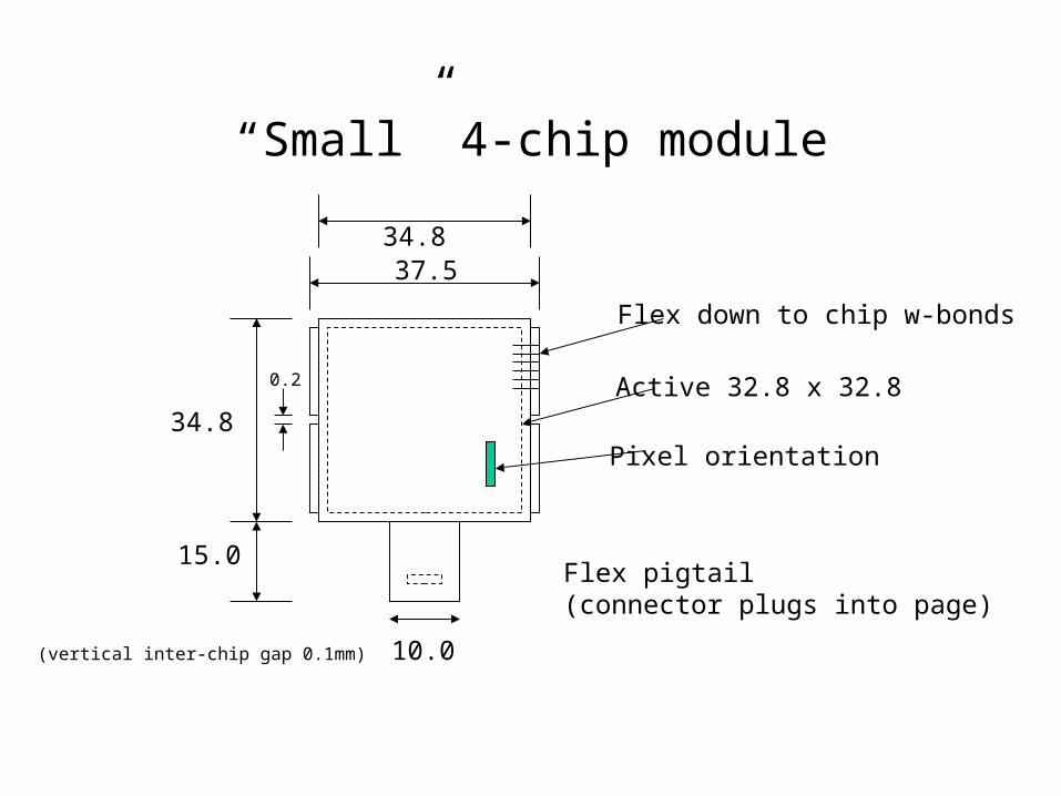
“Small” 4-chip module
34.8
34.8
37.5
Active 32.8 x 32.8
10.0
15.0Flex pigtail (connector plugs into page)
Pixel orientation
Flex down to chip w-bonds
0.2
(vertical inter-chip gap 0.1mm)

“Big” 4-chip module
37.1
37.8
39.9
Active 35.8 x 35.1
10.0
15.0Flex pigtail (connector plugs into page)
Pixel orientation
Flex down to chip w-bonds
0.2
(vertical inter-chip gap 0.1mm)
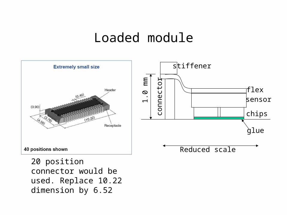
Loaded module
20 position connector would be used. Replace 10.22 dimension by 6.52
glue
chips
sensorflex
conn
ecto
rReduced scale
1.0
mm
stiffener

“Small” module outer stave
…
End of stave card serving 8 modules (half a stave) along ZCan serve one face only (top or bottom) => 4 cards per staveOr can be a wrap-around end of stave card and serve both faces => 2 cards per stave.This way identical staves (including bus cable) design can be used over a wide radial range: 4 cards/stave at lower radius and 2 wrap-around cards per stave at higher radius
34.8 26.8
Module on back
986mm
38.4

“Big” module outer stave
…
End of stave card serving 7 modules (half a stave) along Z (or 8 modules for 1082mm active length)
Can serve one face only (top or bottom) => 4 cards per staveOr can be a wrap-around end of stave card and serve both faces => 2 cards per stave.This way identical staves (including bus cable) design can be used over a wide radial range: 4 cards/stave at lower radius and 2 wrap-around cards per stave at higher radius
37.8 29.8
Module on back
946mm
39.9

“Small” sensor 6 inch wafer
• Active area = 7508 mm^2
• Sensor tiles shown with darker line
• Wafer scale flip chip compatible. Chips shown with lighter line.
• The name “small” 2x2 tile comes from the wafer layout.
– A slightly larger chip and therefore larger 2x2 tile is possible, but only 6 such “large” 2x2 tiles will fit on a 6” wafer.

“Big” sensor 6 inch wafer
• Active area = 7539 mm^2• Sensor tiles shown with darker line
• Wafer scale flip chip compatible.
Chips shown with lighter line.
• OPTION to make 4 6-chip modules per wafer instead of 6 4-chip modules.
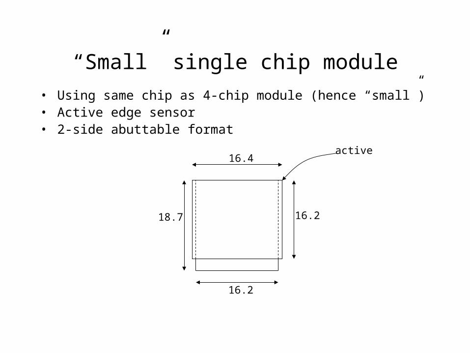
“Small” single chip module
• Using same chip as 4-chip module (hence “small”)• Active edge sensor• 2-side abuttable format
16.4
16.2
16.218.7
active
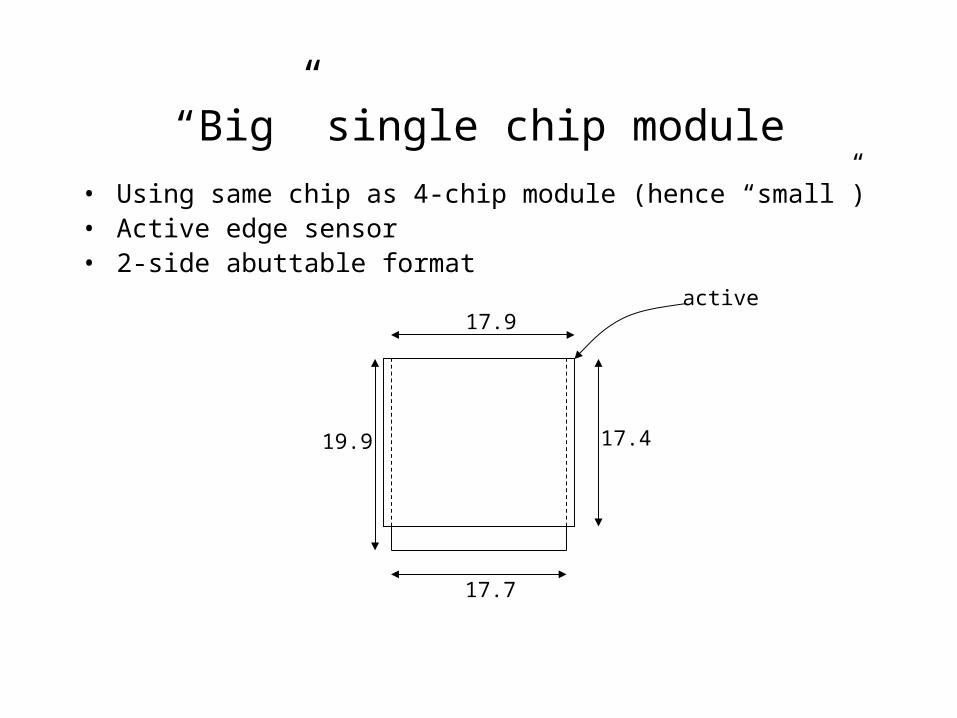
“Big” single chip module
• Using same chip as 4-chip module (hence “small”)• Active edge sensor• 2-side abuttable format
17.9
17.7
17.419.9
active
Top Related