


Languages
Pages
Legal

Form No: 704-C13-01 (000715) BenQ’s Confidence and Property
M100 Circuit Operation Theory (BaseBand)
1. Introduction: 56F52 utilizes TI’s chipsets (CALYPSO-Lite and IOTA) as base-band solution. Base-band is
composed with two potions: Logic and Analog/Codec. CALYPSO-Lite is a GSM/GPRS digital base-band logic solution included microprocessor, DSP, and peripherals. IOTA is a combination of analog/codec solution and power management which contain base-band codec, voice-band codec, several voltage regulators and SIM level shifter etc. In addition, 56E11 integrates with other features such as LED backlight, color LCD display , vibration, melody tone and charging etc. The following sections will present the operation theory with circuitry and descriptions respectively.
2. Block Diagram
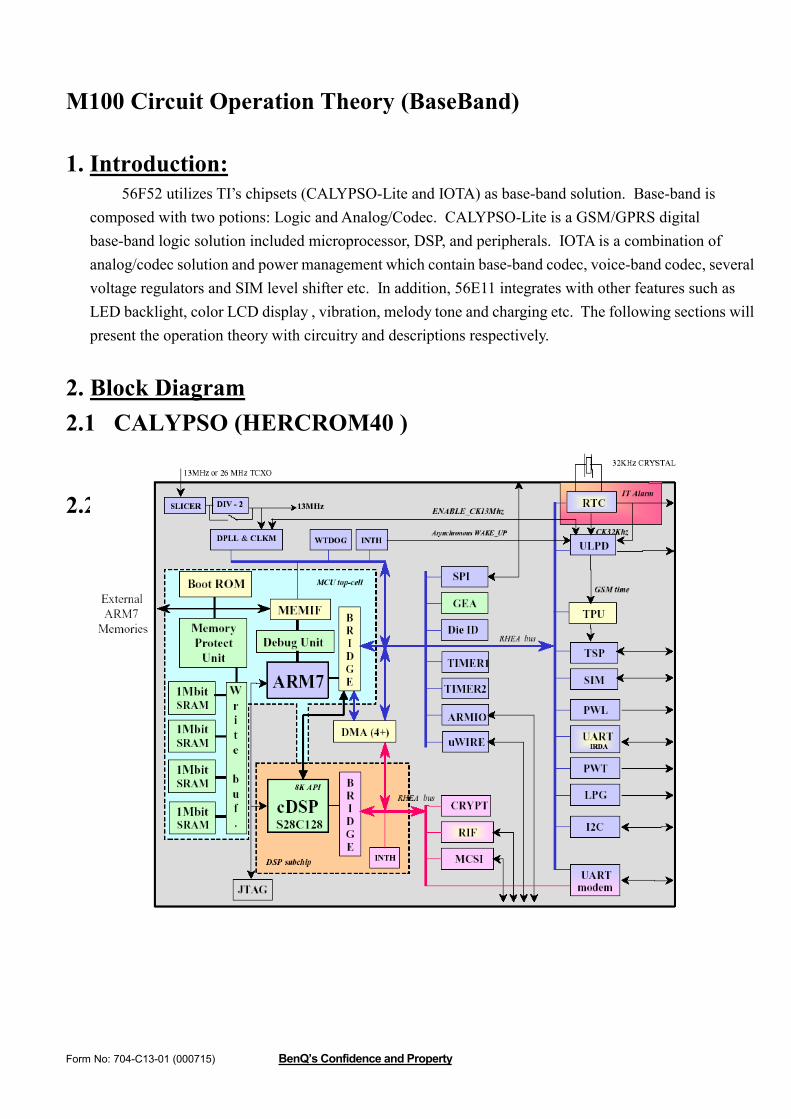
2.1 CALYPSO (HERCROM40 )
2.2 IOTA

Form No: 704-C13-01 (000715) BenQ’s Confidence and Property 1
3. Operation theory:
3.1 Calypso-Lite
CALYPSO-Lite (HERCROM400) is a chip implementing the digital base-band processor of a GSM/GPRS mobile phone. This chip combines a DSP sub-chip (LEAD2 CPU) with its program and data memories, a Micro-Controller core with emulation facilities (ARM7TDMIE) and an internal 2M-bit RAM memory, a clock squarer cell, several compiled single-port or 2-ports RAM and CMOS gates.

Form No: 704-C13-01 (000715) BenQ’s Confidence and Property 2
Major functions of this chip are as follows: 3.1.1 Real Time Clock (RTC)
The RTC block is an embedded RTC module fed with an external 32.768KHz Crystal. Its basic functions are: 1. Time information (seconds/minutes/hours) 2. Calendar information (Day/Month/Year/ Day of the week) up to year 2099 3. Alarm function with interrupts (RTCINT is generated to wake up ABB) 4. 32KHz oscillator frequency gauging
3.1.2 Pulse Width Light (PWL)
This module allows the control of the backlight of LCD and keypad by employing a 4096 bit random sequence .In the 56E11, we use the LT/PWL function to turn on the keypad light LED.
3.1.3 MODEM-UART This UART interface is compatible with the NS 16C750 device which is devoted to the connection to a MODEM through a standard wired interface. The module integrates two 64 words (9 and 11 bits) receive and transmit FIFOs which trigger levels are programmable. All modem operations are controllable either via a software interface or using hardware flow control signals. In 56F52 , we implement software flow control by only two signals: TXD0 and RXD0.
3.1.4 General Purposes I/O (GPIO) Calypso-Lite provides 16 GPIOs configurable in read or write mode by internal registers. In 56F52, we utilize 9 of them as follows, others are used in the dual function mode or N/A:
IO0: N/A IO1: N/A IO2: Interrupt from Melody IC IO3: N/A IO4: N/A IO5: N/A IO6: Detection of earphone or download cable plugged-in
’H’:no accessory plugged-in ’L’: accessory plugged-in
IO7: Reset of external device such as melody IC and CSTN and DSC backend IC IO8: N/A IO9: Backlight of CSTN switch ’H’:ON ,’L’:OFF IO10: N/A IO11: N/A IO12: N/A IO13: N/A
Form No: 704-C13-01 (000715) BenQ’s Confidence and Property 3
IO14: SRAM high-byte enable IO15: SRAM low-byte enable
3.1.5 Serial Port Interface (SPI)
The SPI is a full-duplex serial port configurable from 1 to 32 bits and provides 3 enable signals programmable either as positive or negative edge or level sensitive. This interface is working on 13MHz and is used for the GSM/GPRS baseband and voice A/D, D/A with IOTA
3.1.6 Memory Interface and internal Static RAM For external memory device (Flash and SRAM), this interface performs read and write access with adaptation to the memory width. It also provides 6 chip-select signals corresponding each to an address range of 8 mega bytes. One of these chip-select is dedicated to the selection of an internal memory. In 56E11, we employ nCS0 (NROM_CS0) for external 64 Mbits Flash and nCS1 (NRAM_CS1) for external 16Mbits SRAM. A 2Mbit SRAM is embedded on the die and memory mapped on the chip-select nCS6 of the memory interface .The access cycle is guaranteed with 0 wait-state for any cycle frequency up to 39MHz. About others chip selects allocation are nCS3 (NLCDM_CS3) for LCDM driver and nCS4 for melody IC ..
3.1.7 SIM Interface The Subscriber Identity Module interface will be fully compliant with the GSM 11.11 and ISO/IEC 7816-3 standards. Its external interface is 3 Volts only. 5 Volts adaptation will be based on external level shifters.
3.1.8 JTAG
In 56F52, JTAG is used for software debugging. 3.1.9 Time Serial Port (TSP)
The TPU is a real-time sequencer dedicated to the monitoring of GSM/GPRS baseband processing. The TSP is a peripheral of the TPU which includes both a serial port (32 bits) and a parallel interface. The serial port can be programmed by the TPU with a time accuracy of the quarter of GSM bit. The serial port is uni-directional (transmit only) when used with IOTA. The serial port provides 4 enable signals programmable either as positive or negative edge or level sensitive. This serial port is derived from 6.5MHz and used to control the real time GSM windows for the baseband codec and the windows for ADC conversion.
3.1.10 TSP Parallel interface (ACT)
The parallel interface allows control 13 external individual outputs and 1 internal signal with a time accuracy of the quarter of GSM bit. These parallel signals are mainly used to control the RF activity. In 56F52, we employ 5 of them to control RF activity. TSPACT1: GSM_T/R
Form No: 704-C13-01 (000715) BenQ’s Confidence and Property 4
TSPACT2: DCS_T/R TSPACT3: PCS_RX TSPACT6: TX_ON TSPACT9: Band Select TSPACT10: Latch enable
3.1.11 Radio Interface (RIF)
The RIF (Radio Interface) Module is a buffered serial port derived from the BSP peripheral module of the defined for TMS320C5X. The external serial data transmission is supported by a full-duplex double-buffered serial port interface. The interface is used for transfer of baseband transmit and receive data and also to access all internal programmation registers of the device.
3.1.12 Miscellaneous:
Some important Baseband /RF interface signals are defined as follows: CLKTCXO: 13MHz VTCXO Clock from RF circuit TCXOEN: 13MHz VTCXO Clock Enable signal
3.2 IOTA Together with a digital base-band device (Calypso-Lite), IOTA is part of a TI DSP solution intended for digital cellular telephone applications including GSM 900, DCS 1800 and PCS 1900 standards (dual band capability). It includes a complete set of base-band functions to perform the interface and processing of voice signals, base-band in-phase (I) and quadrature (Q) signals which support single-slot and multi-slot mode, associated auxiliary RF control features, supply voltage regulation, battery charging control and switch ON/OFF system analysis. IOTA interfaces with the digital base-band device through a set of digital interfaces dedicated to the main functions of Calypso-Lite, a base-band serial port (BSP) and a voice-band serial port (VSP) to communicate with the DSP core (LEAD), a micro-controller serial port to communicate with the micro-controller core and a time serial port (TSP) to communicate with the time processing unit (TPU) for real time control. IOTA also includes on chip voltage reference, under voltage detection and power-on reset circuits. Major functions of this chip are as follows: 3.2.1 Baseband Codec (BBC)
The baseband codec includes a two-channel uplink path and a two-channel downlink path. The baseband uplink path (BUL) modulates the bursts of data coming from the DSP via the baseband serial port (BSP) and to be transmitted at the antenna. Modulation is performed by a GMSK modulator.
Form No: 704-C13-01 (000715) BenQ’s Confidence and Property 5
The GMSK modulator implemented in digital technique generates In-phase (I) and Quadrature (Q) components, which are converted into analog base-band by two 10 bits DACs filters. It also includes secondary functions such as DC offset calibration and I/Q gain unbalance. The baseband downlink path (BDL) converts the baseband analog I & Q components coming from the RF receiver into digital samples and filters these resulting signals through a digital FIR to isolate the desired data from the adjacent channels. During reception of burst I & Q digital data are sent to the DSP via the baseband serial port (BSP) at a rate of 270 KHz.
3.2.2 Automatic Frequency control (AFC)
The automatic frequency control function consists of a digital to analog converter optimized for high resolution DC conversion. Its purpose is to control the frequency of the GSM 13MHz oscillator to maintain mobile synchronization on the base station and allow proper transmission and demodulation.
3.2.3 Automatic Power Control (APC) Purpose of the Automatic Power Control (APC) is to generate an envelope signal to control the power ramping up, ramping down and power level of the radio burst. The APC structure is intended to support single slot and multi-slots transmission with smooth power transition when consecutive bursts are transmitted at different power level. It includes a DAC and a RAM in which the shape of the edges (ramp-up and ramp-down) of the envelope signals are stored digitally. This envelope signal is converted to analog by a 10 bits digital to analog converter. Timing of the APC is generated internally and depends of the real time signals coming from the TSP and the content of two registers which control the relative position of the envelope signal versus the modulated I & Q.
3.2.4 Time serial port (TSP)
Purpose of the time serial port is to control in real time the radio activation windows of IOTA which are BUL power-on, BUL calibration, BUL transmit, BDL power-on, BDL calibration and BDL receive and the ADC conversion start. These real time control signals are processed by the TPU of DBB and transmitted serially to ABB via the TSP, which consists in a very simple two pins serial port. One pin is an enable (TEN) the other one the data receive (TDR). The master clock CK13M divided by 2 (6.5MHz) is used as clock for this serial port.
3.2.5 Voice band Codec (VBC)
The VBC processes analog audio components in the uplink path and transmits this signal to DSP speech coder through the voice serial port (VSP). In the downlink path the VBC converts the digital samples of speech data received from the DSP via the voice serial port into analog audio signal. Additional functions such as programmable gain, volume control and side-tone are performed into the voice band codec.
3.2.6 Micro-controller serial port (USP) The micro-controller serial port is a standard synchronous serial port. It consists in three terminals, data transmit (UDX), data receive (UDR) and port enable (UEN). The clock signal is 13MHz clock. The USP

Form No: 704-C13-01 (000715) BenQ’s Confidence and Property 6
receives and sends data in serial mode from and to the external micro-controller and in parallel mode from and to the internal GSM Baseband a Voice A/D D/A modules. The micro-controller serial port allow read and write access of all internal registers under the arbitration of the internal bus controller.
3.2.7 SIM card shifters (SIMS)
The SIM card digital interface in ABB insures the translation of logic levels between DBB and SIM card, for transmission of 3 different signals; a clock derived from a clock elaborated in DBB, to the SIM card (DBBSCK SIMCLK). a reset signal from DBB to the SIM card (DBBSRST SIMRST), and serial data from DBB to SIM card (DBBSIO SIMIO) and vice-vera. The SIM card interface can be programmed to drive a 1.8V and 3 V SIM card
3.2.8 Voltage Regulation (VREG)
Linear regulation is performed by several low dropout (LDO) regulators to supply analog and digital baseband circuits. (1) LDO VRDBB generates the supply voltage (1.85V, 1.5V,and 1.35V) for the digital core of DBB. In
56F52, it is programmed to 1.5V. This regulator takes power from the battery voltage (2) LDO VRABB generates the supply voltage 2.8V for the analog function of ABB. It is supplied by the
battery. (3) LDO VRIO generates the supply voltage 2.8V for the digital core of ABB and digital I/O’s of DBB
and ABB. It is supplied from battery voltage. (4) LDO VRMEM generates the supply voltages 2.8V for DBB memory interfaces I/O’s. (5) LDO VRRAM generates the supply voltages 2.8V for DBB memory interfaces I/O’s (6) LDO VRRTC generates the supply voltages (1.85,1.5, or 1.35V) and supply voltage 1.5V for the
following block of DBB (real time clock and 32K oscillator ). It’s supplied by UPR (7) LDO VRSIM generates the supply voltages (1.8V, 2.9V) for SIM card interface I/O’s
3.2.9 Baseband Serial Port (BSP) The BSP serial interface is used for both configuration of the GSM baseband and voice A/D D/A (read and write operation in the internal registers), and transmission of the radio data to the DSP during reception of a burst by the downlink part of the GSM baseband & voice A/D D/A. Four pins are used by the serial port: BFSR and BDR for receive, BFSX and BDX for transmit. BDX is the transmitted serial data output. BFSX is the transmit frame synchronization and is used to initiate the transfer of the transmit data. BDR is the received serial input. BFSR is the receive frame synchronization and is used to initiate the reception data.
3.2.10 Battery charger Interface (BCI)
The main function of the ABB charger interface is the charging control of either a 1-cell Li-ion Battery or 3-serie Ni-MH cell batteries with the support of the micro-controller. The battery monitoring uses the 10 bit ADC converter from the MADC to measure the battery voltage, battery temperature, battery type, battery charge current, battery charger input voltage. The magnitude of the charging current is set by the
Form No: 704-C13-01 (000715) BenQ’s Confidence and Property 7
10 bits of a programming register converted by an 10 bit Digital to Analog Converter, whose output sets the reference input of the charging current control loop. The battery charger interface performs also some auxiliary functions. They are battery pre-charge, battery trickle charge and back-up battery charge if it is rechargeable.
3.2.11 Monitoring ADC (MADC)
The MADC consists in a 10-bit analog to digital converter combined with a nine inputs analog multiplexer. Out of the nine inputs five are available externally, the four remaining being dedicated to main battery voltage, back up battery voltage, charger voltage and charger current monitoring. On the five available externally three are standard inputs intended for battery temperature, battery type measurements.
3.2.12 Reference Voltage / Power on Control (VRPC)
An integrated band-gap generates a reference voltage. This reference is available on an external pin for external filtering purpose only. This filtered reference is internally used for analog functions. The external resistor connected between pin IBIAS and GNDREF sets, from the band-gap voltage, the value of the bias currents of the analog functions. The VRPC block is in charge to control the Power ON, Power OFF, Switch On, and Switch OFF sequences. Even in Switch OFF state some blocks functions are performed. These “permanent” functions are functions, which insure the wake-up of the mobile such as ON/OFF button detection or charger detection. Interrupts are generated at power-down detection of the PWON button and when abnormal voltage conditions are detected.
3.2.13 Internal bus and interrupt controller (IBIC)
Read and write access to all internal registers being possible via both the BSP and USP, purpose of the internal bus controller is to arbitrate the access on the internal bus and to direct the read data to the proper serial port. During reception of a burst the internal bus controller assign the transmit part of the BSP to the base-band downlink to transfer the I & Q samples to the DSP. This block also handles the internal interrupts generated by the MADC, BCI and VRPC blocks and generates the micro-controller interrupt signal INT2.

Form No: 704-C13-01 (000715) BenQ’s Confidence and Property 8
3.3 Power Supply diagram
R S IM1 .8 /2 .9 V
1 0 m A
R R A M1 .8 /2 .85 0 m A
R M E M1 .8 /2 .8 V
6 0 m A
R D B B1 .3 /1 .5 /1 .8 V
1 2 0 m A
A B BD Ig i ta l
C o r eI /O
A B BA n a lo g
C o r e
R S IM1 .8 /2 .9 V
1 0 m A
R A B B2 .8 V
5 0 m A
B B S
A B BV R P C C o r e
R IO2 .8 V
1 0 0 m A
S IMC A R D
S R A MC O R E
M e n o ryIO
C O R E
D B BM e m o r ie s
I /O
D B BC O re
D B BI /O
D B B B a c k u pR T C
I /O R T C
D B B S p l i t P o w e r
L o w P o w e r D o m a in
V B A T A B B
V C A M
V C M E M
V L M E N
V C D B B
V C I O 1
V C I O 2
V C A B B
V B A T
B A C KU P
V R S IM
V R R A M
V R M E M
V S D B B
V R D B B
V R IO 1
V R IO 2
V R A B B
V L R T C
V R R T C
S e l 1 .8 V
S e l 1 .5 V
3.3.1 Description: The voltage regulators embedded in IOTA consists of seven sub blocks. Several low-dropout (LDO) regulators perform linear voltage regulation. These regulators supply power to internal analog and digital
Form No: 704-C13-01 (000715) BenQ’s Confidence and Property 9
circuit, to DBB processor, and to external memory. · LDO (VRDBB) is a programmable regulator that generates the supply voltages(1.8V,1.5V and 1.3V) for the core of the DBB processor. The main battery supplies VRDBB. · LDO (VRIO) generate the supply voltage (2.8V) for the digital core and I/O of the TWL3014 device. The main battery supplies VRIO. · LDO (VRMEM) is a programmable regulator that generates the supply voltages(2.8V and 1.8V) for external memories (typically flash memories) and DBB memory interface I/O. The main battery supplies VRMEM. · LDO(VRRAM) is a programmable regulator that generate the supply voltages(2.8V and 1.8V) the external memory (typically SRAM memories) and DBB memory interface I/Os. The main battery supplies VRRAM. · LDO (VRABB) generates the supply voltage (2.8V) for the analog functions of the TWL 3014 devices. The main battery supplies VRABB. · LDO (VRSIM) is a programmable regulator that generates the supply voltages (2.9V and 1.8V) SIM card and SIM card devices. The main battery supplies VRSIM. · LDO (VRTC) is a programmable regulator that generate the supply voltage (1.8V.1.5Vand 1.3V) for real time clock and the 32-KHZ oscillator located in the DBB device during all modes. The main or backup battery supplies VRTC.
3.4 System power on/off Sequence 3.4.1 Power on mode
On the plug-in of the valid main battery or backup battery, an internal reset is generated (POR). After a power-on sequence, the TWL3014 device is in the BACKUP or OFF state. When these conditions occur in the power on state, the hardware power on sequence starts: 1. Enable band-gap (VREF and IREF) 2. Check if Main Battery voltage is greater than 3.2V
Form No: 704-C13-01 (000715) BenQ’s Confidence and Property 10
3. Enable charge VRDBB-VRABB-VRMEM-VRRAM 4. Regulator OK. 5. ON_nOFF=1, ABB RSTz=1 6. NRESET pin is set from ‘L’ to ‘H’ 7. 13MHz clock oscillator is enabled
3.4.2 Power off mode
This state is reached when there is not enough voltage in the main battery and backup battery or when both batteries are disconnected. 1. Send INT1 2. Start 5*T watchdog Timer , T= 32K period 3. ON_nOFF=0 4. ABB RSTz=0 5. Disable the LDO’s using MSKOFF content and the band-gap 6. “MBATLOW”=0
3.5 Memory circuit 3.5.1 Description:
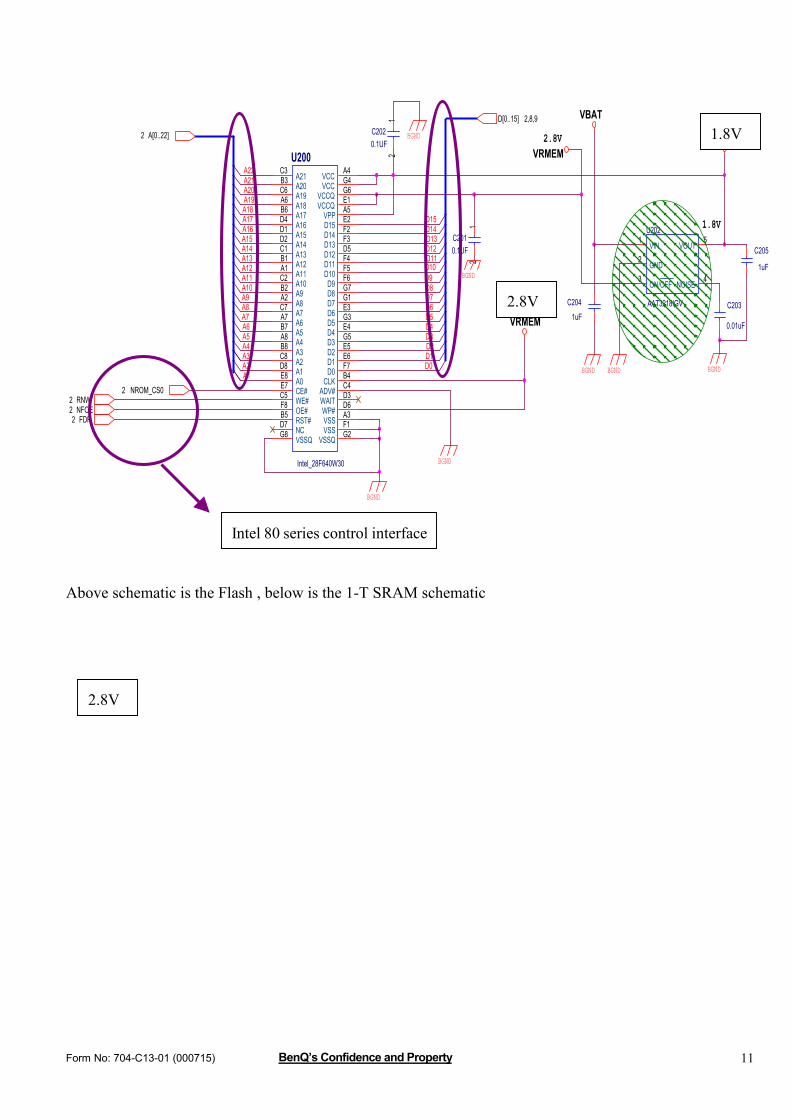
Above diagrams show the memory circuit of 56F52 .One is 64-Mbit core 1.8 Volt , I/O 2.8Volt Intel Wireless Flash Memory W30 series, another is 16M bit 1-T SRAM 3.5.2 Schematic
Address line Data bus
3.3 V<VBAT<4.2V
Form No: 704-C13-01 (000715) BenQ’s Confidence and Property 11
D[0..15] 2,8,9
A3
2.8V
D10
A6
BGND
A22
1.8V
A4
A7
A17
RNW2
A8A9
FDP2
C205
1uF
NROM_CS02
C204
1uF
A19
D6
A5
A15
BGND
BGND
A18
C2020.1UF
12
D3
VRMEM
D11
D15D14
VBAT
C2010.1UF
12
D7
D0
D4
D8
A13
D1
NFOE2
1.8V
D12
C203
0.01uF
A21
A12
A14
D9
A20
BGND
A16
A1A2
U202
AAT3218IGV
1
2
3 4
5VIN
GND
ON/OFF NOISE
VOUT
A[0..22]2
BGND
D5
A10
U200
Intel_28F640W30
C3B3C6A6B6D4D1D2C1B1A1C2B2A2C7A7B7A8B8C8D8E8E7
A4
A5
G6E1
E2F2F3D5F4F5F6G7G1E3G3E4G5E5E6F7
C5F8
G4
B4C4D3D6
B5D7
A3
G2G8F1
A21A20A19A18A17A16A15A14A13A12A11A10A9A8A7A6A5A4A3A2A1A0CE#
VCC
VPP
VCCQVCCQ
D15D14D13D12D11D10D9D8D7D6D5D4D3D2D1D0
WE#OE#
VCC
CLKADV#WAITWP#
RST#NC
VSS
VSSQVSSQVSS
D13
BGND
A11
VRMEM
D2
BGND
Above schematic is the Flash , below is the 1-T SRAM schematic
2.8V
1.8V
2.8V
Intel 80 series control interface

Form No: 704-C13-01 (000715) BenQ’s Confidence and Property 12
A5
A3
A10D14
D11
D9
VRRAM
D7
A14
D6A1
A6
NBLE
D8
A15
A9
D5
MB82D01161-85L_16M
A7
D[0..15]2,5,7
A12D15
NBHE2
EM56161_8M_6T
BGND
D1
A4
A17
SV6P8016_8M_1T
A19
D13
LP62S16256E-T_4M_6T
D0
A[0..22] 2
NFOE2
D4
A20
A13
SV6P4016_4M_1T
D2
U201
IC SRAM SV6P1615UFA70I FBAG48
B6C5C6D5E5F5F6G6B1C1C2D2E2F2F1G1
A1
A3A4A5B3B4C3C4D4H2H3H4H5G3G4F3F4E4D3
G5
B5A6B2
A2
E1
D1E6
D6
E3
H1G2H6
I/O0I/O1I/O2I/O3I/O4I/O5I/O6I/O7I/O8I/O9I/O10I/O11I/O12I/O13I/O14I/O15
LB
A0A1A2A3A4A5A6A7A8A9
A10A11A12A13A14A15A16A17
WE
CE1CE2HB
OE
VCC
GNDGND
VCC
GND
A18A19A20
BGNDK6F1616U6A_16M
D12
A11RNW2
A21
C200
1uF
A8
NRAM_CS1
2A16
A2
A18
D10
D3
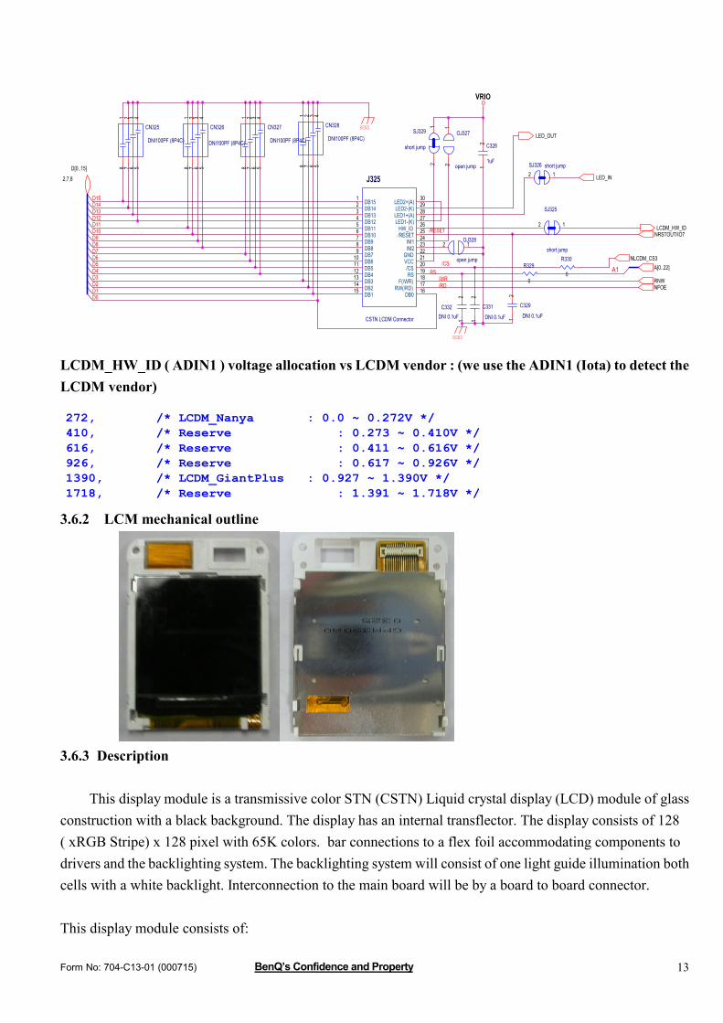
3.6 LCD module ( LCDM) 3.6.1 Connector between PCBA and LCDM
Form No: 704-C13-01 (000715) BenQ’s Confidence and Property 13
D5
SJ326 short jump12
NFOE
C331
DNI 0.1uF12
VRIO
LED_IN
/WR
/CS
SJ329
short jump
12
D7
D9
D12
LED_OUT
D6
CN325
DNI100PF (8P4C)
1 2 3 45678
C329
DNI 0.1uF12
D8OJ328
open jump
12
BGND
A[0..22]
BGND
D15
D3
CN328
DNI100PF (8P4C)
1 2 3 45678D[0..15]
2,7,8
C328
1uF
12
D10D11
OJ327
open jump
12
C332DNI 0.1uF 1
2
NRSTOUT/IO7LCDM_HW_ID
CN327
DNI100PF (8P4C)
1 2 3 45678
/RESET
R329
0
D13
NLCDM_CS3R330
0
D1
RS
D14SJ325
short jump
12
D4
CN326
DNI100PF (8P4C)
1 2 3 45678
/RD
A1RNWD2
J325
CSTN LCDM Connector
123456789
101112131415 16
1718192021222324252627282930DB15
DB14DB13DB12DB11DB10DB9DB8DB7DB6DB5DB4DB3DB2DB1 DB0
RW(/RD)F(/WR)
RS/CS
VCCGND
IM2IM1
/RESETHW_ID
LED1-(K)LED1+(A)LED2-(K)LED2+(A)
D0
LCDM_HW_ID ( ADIN1 ) voltage allocation vs LCDM vendor : (we use the ADIN1 (Iota) to detect the LCDM vendor)
272, /* LCDM_Nanya : 0.0 ~ 0.272V */410, /* Reserve : 0.273 ~ 0.410V */616, /* Reserve : 0.411 ~ 0.616V */926, /* Reserve : 0.617 ~ 0.926V */1390, /* LCDM_GiantPlus : 0.927 ~ 1.390V */1718, /* Reserve : 1.391 ~ 1.718V */
3.6.2 LCM mechanical outline
3.6.3 Description
This display module is a transmissive color STN (CSTN) Liquid crystal display (LCD) module of glass construction with a black background. The display has an internal transflector. The display consists of 128 ( xRGB Stripe) x 128 pixel with 65K colors. bar connections to a flex foil accommodating components to drivers and the backlighting system. The backlighting system will consist of one light guide illumination both cells with a white backlight. Interconnection to the main board will be by a board to board connector. This display module consists of:

Form No: 704-C13-01 (000715) BenQ’s Confidence and Property 14
CSTN Cell with polarizers, COG
Enhancement films (DBEF + 2*BREF)
Mechanical support/carrier system with Magnesium frame
One illumination system with 2 White LED’s.
Flexfoil with SMD component (include board to board connector for connection to the main part of the phone and between the module)
3.6.4 White LED driver schematic
C33
3C
12
C325
1uF(0603)
12
LED_OUT
BGND
BL325
BEAD(0603) U325
MIC 2287 WHITE LED DRIVER
3
4 5
8
7
6
1
2
EN
AGND NC
PGND
SW
FB
OVP
VIN
NLED_DRIVE_SD/IO9
BGND
D325RB520S-30
12
C32
6
1uF
(060
3)
12
R328
82K
12
R326
3.9
12
BGND
BGND
R327
4.7K
12
DAC
C327
1uF (0603)
12
BGND
VBAT
R331
47K
12
LED_IN
L325
33uH
3.7 Audio circuit 3.7.1 Uplink path
Max 20mA
2.0V
DAC range 0~1023 step

Form No: 704-C13-01 (000715) BenQ’s Confidence and Property 15
C165 0.1UF
68ohm
47pF
EN150EMI Array
C1
C3
A1
A3
B2
C1600.1UF
TP150
1
MICIN
R172 1K
R162 1K
TP151
1
R164
1K
T150
DNI
12
..
BGND
C168DNI
12
BGND
R173 1K
MICBIAS
C1694.7uF(0603)
BGND
R163
1K
X150MICROPHONE_0
34
T151DNI
12
..
MICIP
3.7.2 Downlink path
C182
27PF
C181
27PF
RECEVER_P 9
RECEVER_N 9
BGND
EARP+
BGND
EARN-
BGND
RECEVER_N
T400TVS
12
..
T401TVS
12
..
RECEVER_P
SJ402 short jump
12
RECEIVER+
LS1
Receiver
TP400
1
RECEIVER-
SJ403 short jump
12
TP401
1
-10dBm0
-10dBm0
Iota part

Form No: 704-C13-01 (000715) BenQ’s Confidence and Property 16
3.7.3 Description
The audio circuit is divided into two parts, uplink and downlink path. For uplink path, the analog voice signals are fed into IOTA from the microphone differential input and
then transmitted to G2 DSP via the voice-band series port (VSP). After being modulated, the signals go through the uplink I/Q path to the RF transceiver and transmitted from the antenna.
The microphone circuit is biased from MICBIAS of IOTA. The bias circuit, R163, R164, R162 mainly provides the optimal operation point for the microphone signals, MICP and MICN. For downlink path, the signals received from the antenna are down-converted to I/Q signals and then transmitted to G2 DSP. After being demodulated, the signals are fed to IOTA via voice-band interface and then amplified to drive the receiver in the EARP and EARN .
3.8 Melody IC 3.8.1 Schematic
Yamaha 16 tone melody IC

Form No: 704-C13-01 (000715) BenQ’s Confidence and Property 17
VRIO
R4050
1 2
VBAT
R40
1
3.3k
12
RNW2
BGND
R404
62K
12
C405
0.1uF
12
NFOE2
D0
C407
270pF
12
A[0..22]2
D3
LOUD_SPK_N 9
C40
14.
7uF(
0603
)
12
SJ401 short jump
12
NRSTOUT/IO72
C404
0.1uF
D4
U400
YMU759
1 2 3 4 5 6 7 8 9
10
14
16
11
13
171819202122232425
26
27
28
29
3012
15
31
32
CLK
1
EX
T1
/IRQ
/RS
T
IFS
EL
PLL
C
VD
D
VS
S
VR
EF
HPOUT-L/MONO
EQ3
SPVSS
HPOUT-R
EQ2
SP
OU
T1
SP
OU
T2
EX
T2D7
D6
D5
D4
D3
D2
D1
D0
/WR
/CS
A0EQ1
SPVDD
/RD
SDOUT
D5
D7
VRIO
A1
TPL400 1
R40320K
1 2
NMELODY_INT/IO22
D2
LOUD_SPK_P 9
D1
D[0..15]2,4,9
C406
4.7uF
12
Gain = R407 / R404f1 = 1 / (2pi * R412 * C404)f2 = 1 / (2pi * R414 * C407)
BGND
D6
13MOUT3
C40
0
1nF
12
NMELODY_CS42
3.8.2 Description: The Yamaha Melody IC (YMU759 MA2) mainly generate multi-tone for speaker. The main features are 1. Equipped with FM generator function and ADPCM playback function 2. Number of voice simultaneously generated
When only 2-operator tone are used : up to 16 voices can be generated simultaneously When only 4-operator tone are used : up to 8 voices can be generated simultaneously
3. Built-in 4-bit 1ch ADPCM decoder, and supports two kinds of sampling frequency , 4kHz and 8kHz. 4. Built-in output 550mW (AVDD=3.6V) speaker amplifier 5. Built-in hardware sequencer 6. Built-in circuit for sound quality correcting equalizer 7. Supports stereophonic D/A converter 8. Provided with a stereophonic analog output terminal for headphone

Form No: 704-C13-01 (000715) BenQ’s Confidence and Property 18
9. 4 wire serial interface or 12 wire parallel interface can be selected 10. PLL is built-in to support master clock in 2MHz to 20MHz range 11. Support power down mode(Typical current: 1uA or less) 12. Power supply is divided into analog power supply for speaker amplifier and power supply for the others
Analog power supply for speaker amplifer (SPVDD): 2.7V~4.5V (Typ 3.6V) Digital power supply for the others (VDD):2.7V~3.3V(Typ 3.0V)
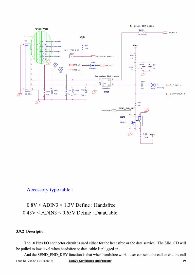
3.9 10 Pins I/O connector 3.9.1 Schematic
Form No: 704-C13-01 (000715) BenQ’s Confidence and Property 19
TXD 2,3
SEND_END_KEY
R451
1K
12
BL450
BEAD(0603)
R466
100K
ACCESSORY_IN/IO6 2
EARPHONE_IN 3
R457
300
SP2 Discharging component
1 2
BGND
R452
2K
20.N2003.010
T451
TVS 12
..
尖端放電
TP450
1
VRIO
R453
100K
VRIO
BGND
C450
1uF
BGND
T452
TVS
12
..
U452
PEMH2
16
2 345
BGND
SJ450 short jump
12
T453
TVS
12
..
R456
300
J450
I/O CONN
1
2
3
4
5
6
7
8
9
1011
12
U451CSPEMI204
A1
B2A3 C3
C1I1
GNDI3 O3
O1
R455
10K
SP3 Discharging component
1 2
To solve TDD issue
SIM_CD 2
To solve TDD issue
SJ451
short jump
1 2 C451
DNI
12
SEND_END3
BGND
BGND
SP1 Discharging component
1 2
RXD 2,3
BGND C452
4.7uF
12
SP4 Discharging component
1 2
VRIO
T450
TVS12
..
HF_HSO 3
HF_AUXI 3
T454
TVS
12
..
/放大 工廠量產
Accessory type table : 0.8V < ADIN3 < 1.3V Define : Handsfree
0.45V < ADIN3 < 0.65V Define : DataCable
3.9.2 Description
The 10 Pins I/O connector circuit is used either for the headsfree or the data service. The SIM_CD will be pulled to low level when headsfree or data cable is plugged-in.
And the SEND_END_KEY function is that when handsfree work , user can send the call or end the call
Form No: 704-C13-01 (000715) BenQ’s Confidence and Property 20
in the handsfree push bottom key. This function use the Keypad interrupt (G2-Lite) to generate the send-end function.
The HF_HSO is the handsfree speaker output and the HF_AUXI is the handsfree Micphone input for the Iota.
The EARPHONE _IN is connected to the Iota ADIN3 to judge accessory type (refer to the Accessory type table)
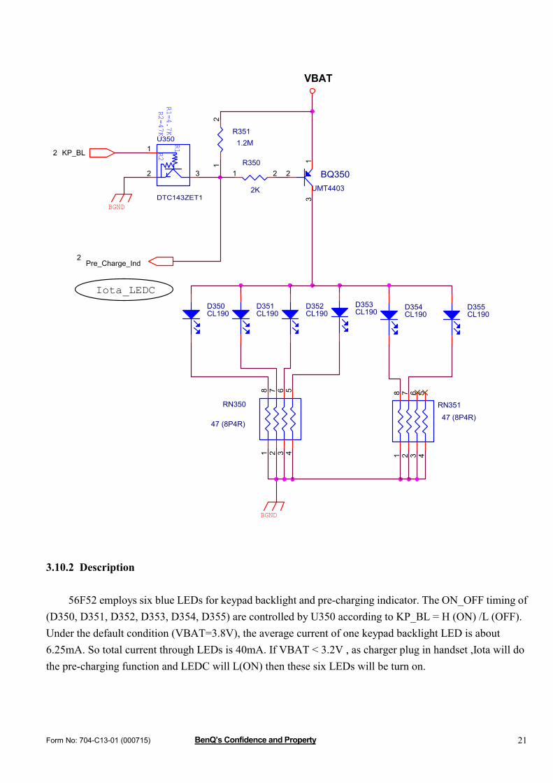
3.10 Keypad LED circuit 3.10.1 Schematic
Form No: 704-C13-01 (000715) BenQ’s Confidence and Property 21
Pre_Charge_Ind2
BGND
D352CL190
Iota_LEDCD350CL190
RN351
47 (8P4R)
1 2 3 45678
D353CL190
R3511.2M
12
BGND
D355CL190
BQ350UMT4403
2
13
D354CL190
KP_BL2
VBAT
RN350
47 (8P4R)
1 2 3 45678
R1R2R1=4.7KR2=47K
U350
DTC143ZET1
2
1
3R350
2K
1 2
D351CL190
3.10.2 Description
56F52 employs six blue LEDs for keypad backlight and pre-charging indicator. The ON_OFF timing of (D350, D351, D352, D353, D354, D355) are controlled by U350 according to KP_BL = H (ON) /L (OFF). Under the default condition (VBAT=3.8V), the average current of one keypad backlight LED is about 6.25mA. So total current through LEDs is 40mA. If VBAT < 3.2V , as charger plug in handset ,Iota will do the pre-charging function and LEDC will L(ON) then these six LEDs will be turn on.
Form No: 704-C13-01 (000715) BenQ’s Confidence and Property 22
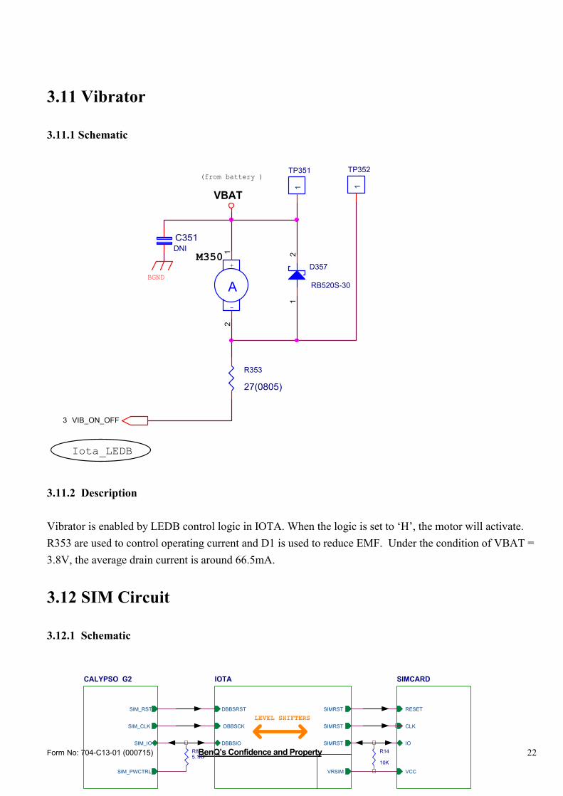
3.11 Vibrator 3.11.1 Schematic
M350
(from battery )TP351
1A-
+
12
C351DNI
R353
27(0805)
Iota_LEDB
VBAT
D357
RB520S-301
2
BGND
VIB_ON_OFF3
TP352
1
3.11.2 Description Vibrator is enabled by LEDB control logic in IOTA. When the logic is set to ‘H’, the motor will activate. R353 are used to control operating current and D1 is used to reduce EMF. Under the condition of VBAT = 3.8V, the average drain current is around 66.5mA.
3.12 SIM Circuit 3.12.1 Schematic
IOTA
DBBSRST
DBBSCK
DBBSIO
SIMRST
SIMRST
SIMRST
VRSIM
CALYPSO G2
SIM_RST
SIM_CLK
SIM_IO
SIM_PWCTRL
SIMCARD
RESET
CLK
IO
VCC
R85.1KF
R14
10K
LEVEL SHIFTERS
Form No: 704-C13-01 (000715) BenQ’s Confidence and Property 23
3.13.2 Description
The SIM interface of IOTA is composed by a dedicated LDO and I/O level shifters. It supports 3V and 1.8V SIM cards (In 56E11 just use the 3V ).
SIM_IO(I/O): Data SIM_RST(O): Reset signal SIM_CLK(O): Clock (1.6MHz/3.2MHz)
The SIM card digital interface insures the translation of logic levels between CALYPSO-Lite and SIM card. Selection of pull-up resistor is trade-off between the SIM IO rising time and current consumption
3.13 Keypad 3.13.1 Schematic

Form No: 704-C13-01 (000715) BenQ’s Confidence and Property 24
S371
KSW[End][PWR]
ROW02
PWON 2
S352KSW[1]
S365KSW[#]
BGND
COL22
S361KSW[8]
S358KSW[left]
SEND_END 2
S367KSW[*)]
S353KSW[Down]
COL12
COL32
S364KSW[SEND]
D356
RB520S-30
1 2
CN350
DNI
1 2 3 45678
ROW22
S351KSW[2]
COL02
TP350
1
S362KSW[7]
S368KSW[Right]
Fixture
S356KSW[5]
S354KSW[Menu]
S355KSW[6]
S360KSW[9]
C350
DNI
12
S366KSW[0]
S357KSW[4]
ROW42
ROW12
BGNDTP355
1
S369KSW[QUIT]
S363KSW[Up]
S359KSW[SEL]
BGND
S350KSW[3]
ROW32
3.13.2 Description 1. The keypad is made of a 5 Column x 5 Row matrixes. 2. The keypad matrix is as follows:
Function Key COL0 COL1 COL2 COL3 COL4 ROW0 ROW1 ROW2 ROW3 ROW4
END/PWR S371
3 S350 0 0
2 S351 0 0
1 S352 0 0
DOWN S353 0 0
MENU S354 0 0
6 S355 0 0
5 S356 0 0
Form No: 704-C13-01 (000715) BenQ’s Confidence and Property 25
4 S357 0 0
LEFT S358 0 0
YES/Send S359 0 0
8 S361 0 0
7 S362 0 0
UP S363 0 0
SEND S364 0 0
9 S360 0 0
# S365 0 0
0 S366 0 0
* S367 0 0
RIGHT S368 0 0
NO S369 0 0
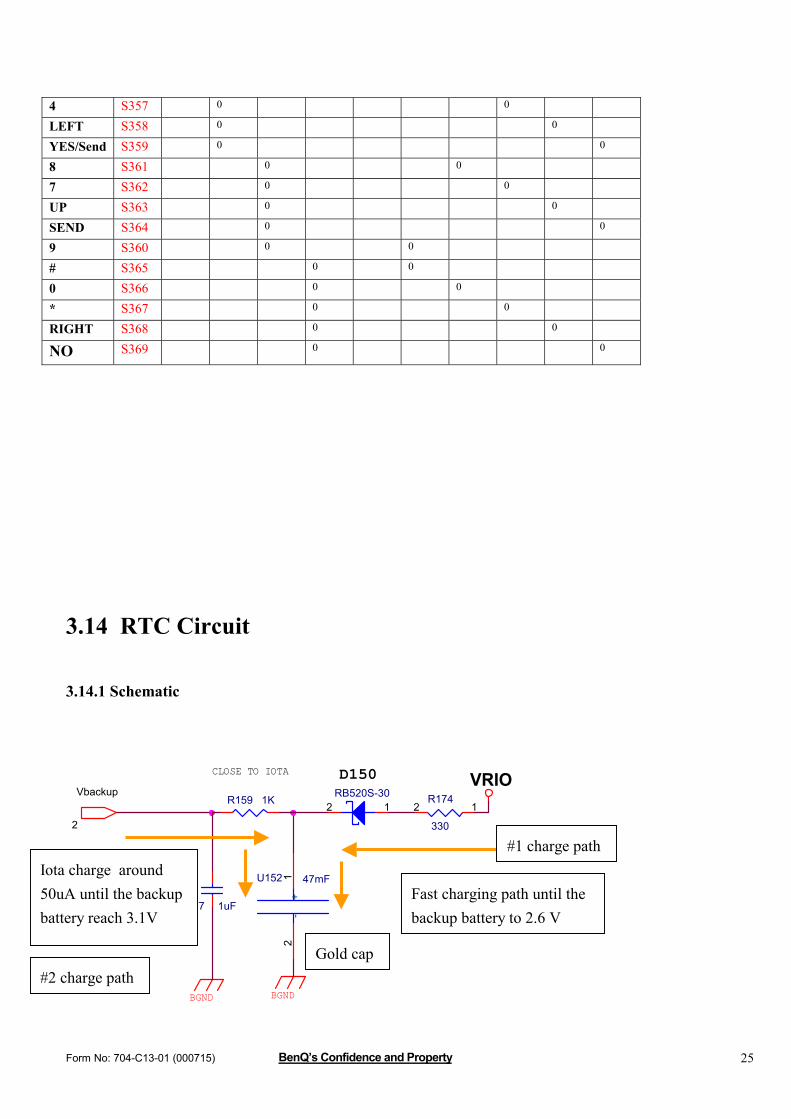
3.14 RTC Circuit 3.14.1 Schematic
U152 47mF12
+-
R159 1K
CLOSE TO IOTA
C177 1uF
BGND
RB520S-3012
BGND
VRIOR174
330
12Vbackup
2
D150
Fast charging path until the backup battery to 2.6 V
Iota charge around 50uA until the backup battery reach 3.1V
Gold cap
#1 charge path
#2 charge path
Form No: 704-C13-01 (000715) BenQ’s Confidence and Property 26
3.14.2 Description
Gold cap is employed as backup battery. When main battery is removed or battery voltage is lower than
backup battery voltage, backup battery will supply real-time clock and the 32.768Hz oscillator. The supply current for backup battery is about 50uA. There are two charging paths for backup battery. The charge path #1 charge backup battery until backup battery voltage reachs around 2.6V. The charge path #2 is always on until backup battery is full-charged
3.15 Charging circuit 3.15.1 Schematic
DZ250
UDZS6.2B
VBAT
BGND
F250
FUSE(1A 0603)
BGND
R25824K
BGND
SJ250
0
BGND
BATEMP3
TP2521
R252
5.1K
(060
3)
TP251
1
R1=47K
BGND
T251
TVS
12
..
C257
DNI
G1S2G2
D2 S1 D1 U251FDC6506P
16
34 5
2
fromIOTA's BCI
PWR
C258
0.1uF
R2=47K
BGND
R1
R2R1=4.7KR2=47K
U253DTC143ZET1
2 1
3
TP250
1
JP250
BATTERY CONNECTOR
1
2
3
VBAT
BATTEMP
GND
ICTL 3
VBATBB
VCHG
U252
XC61CC4302NR
3
4
2
1
NC
Vss
Vin
Vout
R260 (0805)
9112
BGND
R257 (0805)
9112
C2550.1uF
12
D250
CRS03
1 2
BGND
VCCS3
T250
DNI
12
..
PCHG3
BGND
R251
1K
U255PEMH2
16
2 345
BQ250BC807-40W
1
23
C259
1uF
J250
Power Jack
1
2
3
4
GND
V+
GND
GND
BGND
R256
0.2(1%) 0805
TP253
1
C251
22pF
VBAT
BGND
RPWON
BGND
C254
0.1uF
C2500.1uF
( to IOTA for BB power)
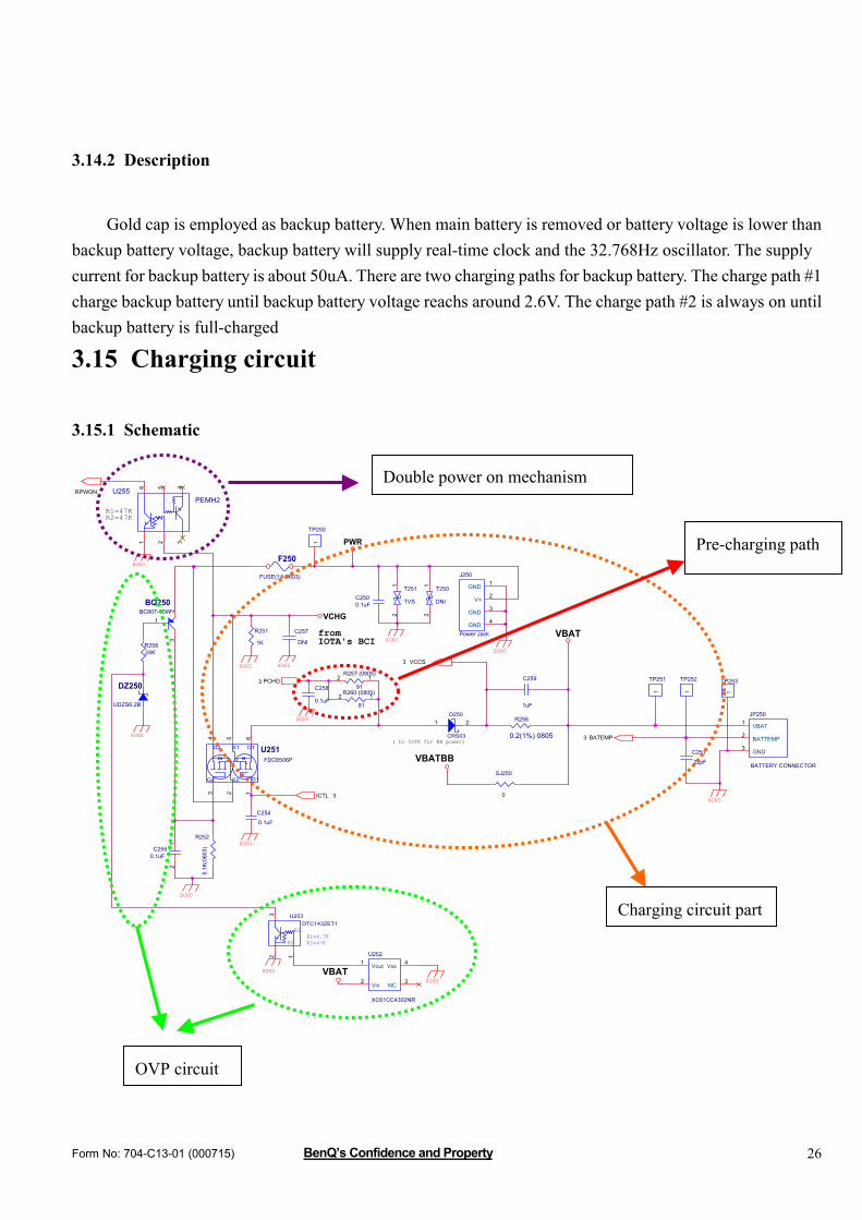
OVP circuit
Charging circuit part
Double power on mechanism
Pre-charging path

Form No: 704-C13-01 (000715) BenQ’s Confidence and Property 27
3.15.2 Description
This circuit mainly contains OVP, Charge circuit part , and Double power on mechanism . The OVP
gives system a voltage protection of over charger voltage or battery over charged. If the charger voltage is over 6.8 V and the battery is over charged to 4.4 V the OVP mechanism will work.
F250 is a 1A fuse to assure charging current under 1A limit. The group of BQ250 and DZ250 compose the charger over-charge protection circuit. The cut-off voltage is 6.8V. While the charger voltage is over 6.8V, the circuit will turn off U251 PMOS to stop charge process. The group of 253, BQ250 and U252 compose the battery over-charge protection circuit. While the battery voltage is over 4.4V, the circuit will turn on U252 to turn off U251 PMOS to stop charge process.
The normal charging operation theory (battery voltage above 3.2V) is that IOTA monitors charger voltage via VCHG pin to decide whether charger plug in or out, and control power P-MOSFET (U251.1) via ICTL pin. If phone enters into charging mode, the ICTL pin will limit the maximum charging current at 750mA(max) by sensor the R256 and control CC_H / CC_L mode. When VBAT equals to 4.2V, Iota will stop the charge function . The charging current will decrease until the charging current is lower than 30mA. In charging process, IOTA BCI always monitor the charging status. It can monitor charging current by current sense resistor (R256), VBAT and temperature by ADC pin, and charging time by internal timer. If there is any abnormal status happened while charging, IOTA BCI will turn off power P-MOSFET (U251.1) via ICTL pin to prevent any hazardous condition happening.
When VBAT<3.2V, charging state enters in “pre-charge” state. In this state, U251 is off and IOTA will supply pre-charge current from VCHG through VBAT to charge battery. We use R257 and R260 to set the pre-charge current between 35mA(VBAT=3V) to 75mA(VBAT=2V).
Double power on mechanism , this mechanism is to avoid the VCHG > Vbat power on function fail , therefore we use the Remote power on function to double turn on the power on sequence.
56E11 Li-ion 760mAH Battery Charging Algorithm Linear Charger: 3.6V & 600mA
Form No: 704-C13-01 (000715) BenQ’s Confidence and Property 28
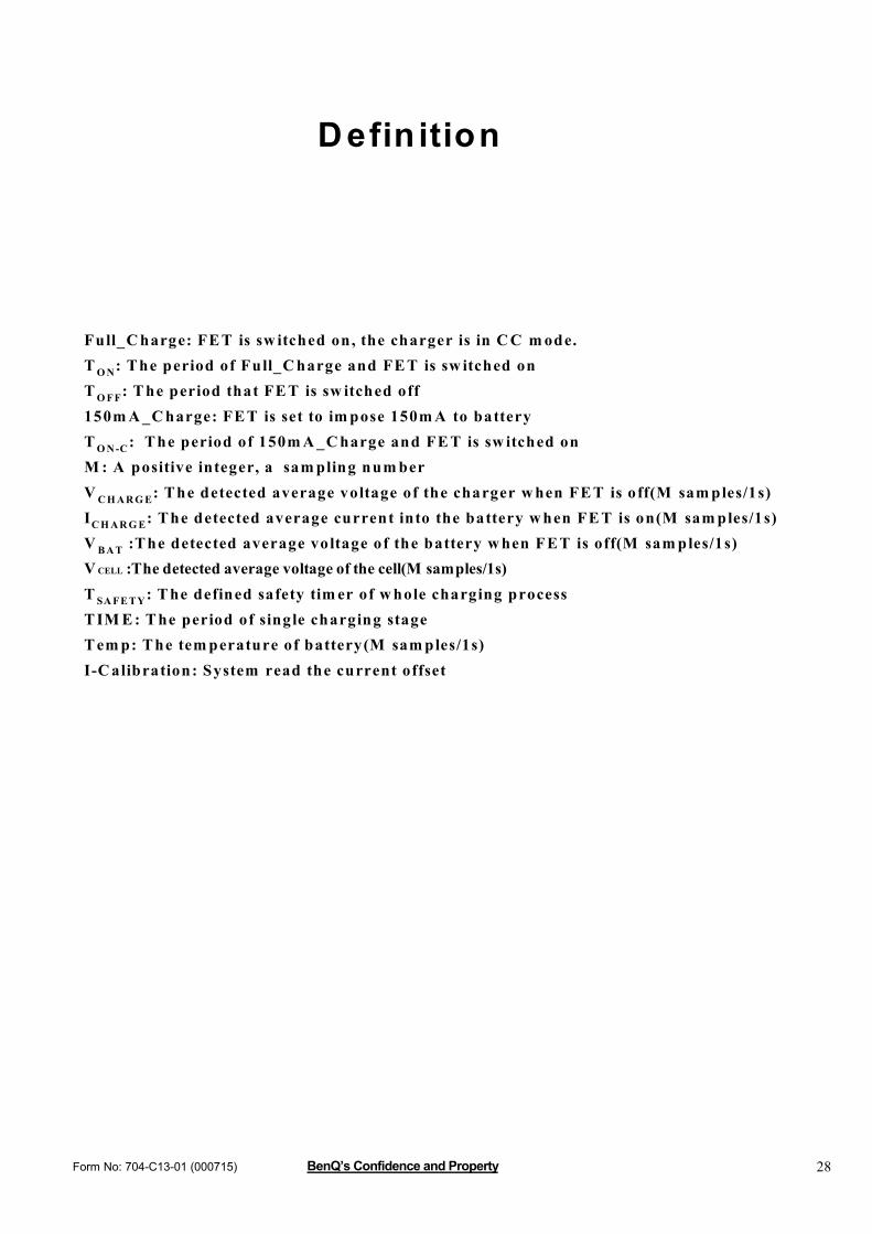
Full_C harge: FE T is sw itched on, the charger is in C C m ode.T O N: The period of Full_C harge and FE T is sw itched onT O FF: T he period that FE T is sw itched off150m A _C harge: FE T is set to im pose 150m A to batteryT O N-C: The period of 150m A _C harge and FE T is sw itched onM : A positive integer, a sam pling num berV C H AR G E: The detected average voltage of the charger w hen FE T is off(M sam ples/1s)IC H AR G E: The detected average current into the battery w hen FE T is on(M sam ples/1s)V B AT :The detected average voltage of the battery w hen FET is off(M sam ples/1s)V CELL :The detected average voltage of the cell(M samples/1s)T SA FE TY: T he defined safety tim er of w hole charging processT IM E : T he period of single charging stageT em p: The tem perature of battery(M sam ples/1s)I-C alibration: System read the current offset
Defin ition

Form No: 704-C13-01 (000715) BenQ’s Confidence and Property 29
System Power On
VCHARGE
< 6.5V
error message
Software Charging Flow
CHECK = 0
CC mode
No(If CHECK=1,
error1)(If CHECK=2,
error2)
Yes
Yes
No(error 1)
VBattery
< 4.4V
Yes
No(error 3)
Calibration CheckSubroutine
Yes
Form No: 704-C13-01 (000715) BenQ’s Confidence and Property 30
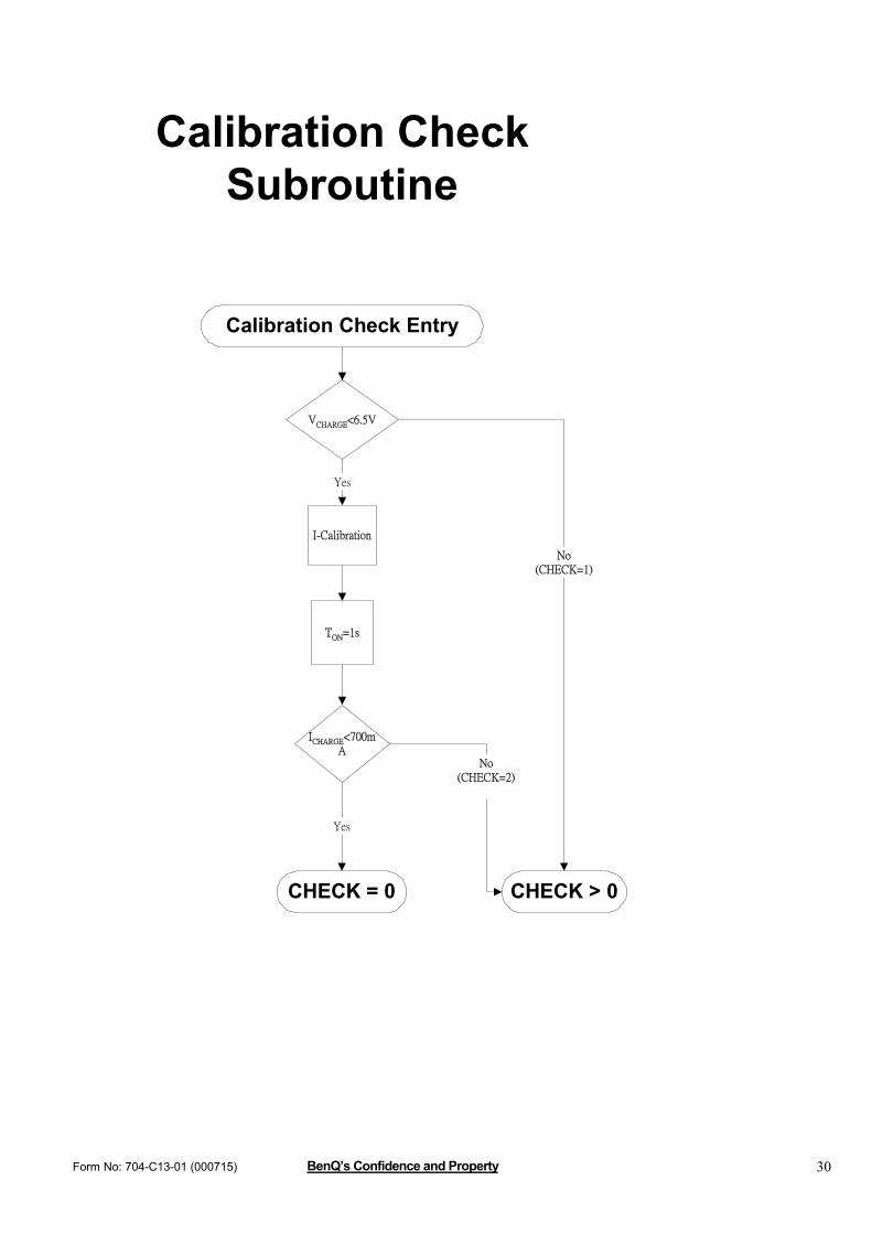
Calibration CheckSubroutine
ICHARGE<700mA
VCHARGE<6.5V
TON=1s
Calibration Check Entry
CHECK = 0
I-Calibration
No(CHECK=1)
Yes
Yes
No(CHECK=2)
CHECK > 0

Form No: 704-C13-01 (000715) BenQ’s Confidence and Property 31
if LINK
TIME<2 hours
NO
NO(error6)
YES
VBAT<4.18V
YES
YES
NO
VBAT<3.8V
YES
YES
TIME=0
NO
YES
CHECK_ON=1
CHECK_OFF=1
CHECK_ON=1
CHECK_OFF=1
TIME<1 hours
YES NO(error6)
NO
NO
VBAT<3.8V
NO
CC mode Entry
NO
CC_Lowmode Entry
TIME=0
TSAFETY=0
CC mode
errormessage
errormessage
TON=5sFull-Charging
On Check
TOFF=1sOff Check
YES
TON=5sFull charging
On Check
TOFF=1sOff Check
No
if FunLight on
VBAT
<3.9VNo
Yes
Yes
No
Yes
Yes
if FunLight on
No
Yes

Form No: 704-C13-01 (000715) BenQ’s Confidence and Property 32
TIME=0
YESCHECK_ON=1
CHECK_OFF=1
TIME<2 hours
YES
NO(error6)
NO
NO
VBAT
<4.199V
if LINKor FunLight on
YES
NO
errormessage
Yes
Ton = 5s150mA_charge
On Check
Toff = 1sOff Check
YES
CC_Low modeEntry
CC_Low mode
CC mode Entry
Form No: 704-C13-01 (000715) BenQ’s Confidence and Property 33
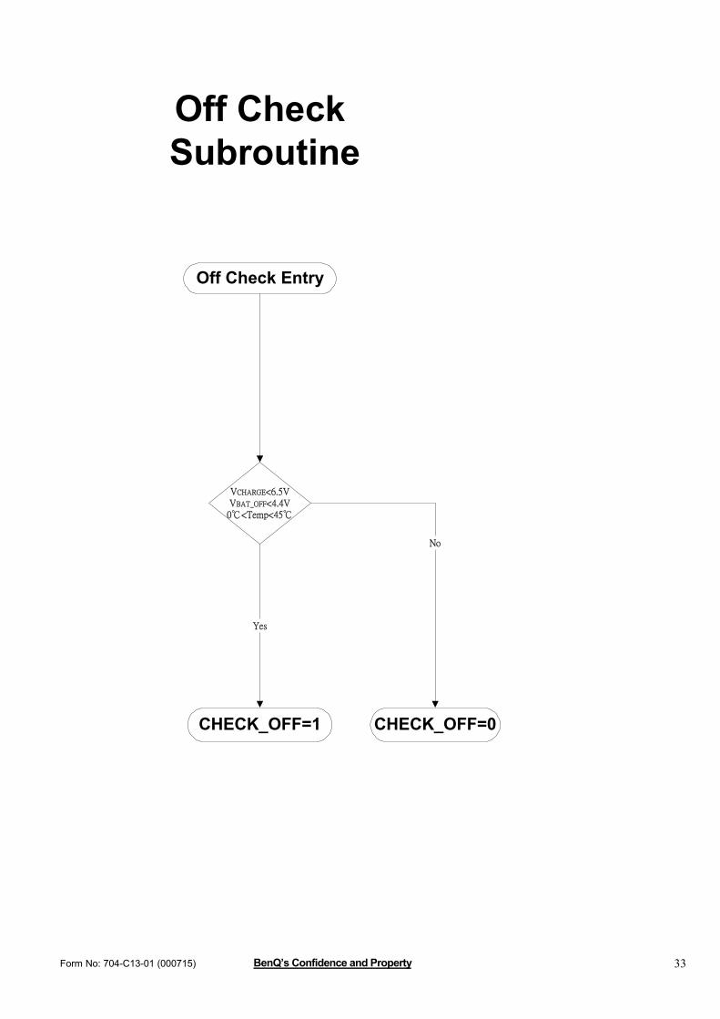
Off Check Subroutine
VCHARGE<6.5VVBAT_OFF<4.4V
0℃<Temp<45℃
CHECK_OFF=1 CHECK_OFF=0
Yes
Off Check Entry
No
Form No: 704-C13-01 (000715) BenQ’s Confidence and Property 34
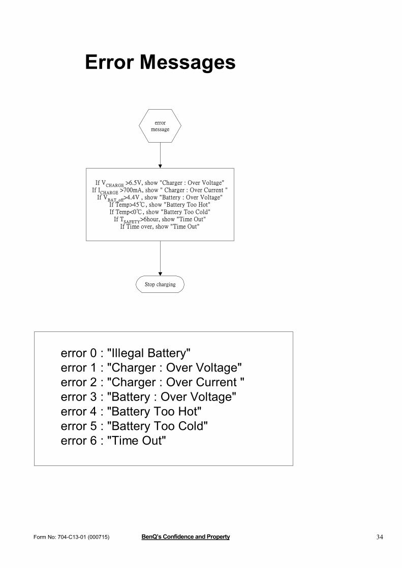
Stop charging
Error Messages
errormessage
error 0 : "Illegal Battery"error 1 : "Charger : Over Voltage"error 2 : "Charger : Over Current "error 3 : "Battery : Over Voltage"error 4 : "Battery Too Hot"error 5 : "Battery Too Cold"error 6 : "Time Out"
If VCHARGE
>6.5V, show "Charger : Over Voltage"If I
CHARGE >700mA, show " Charger : Over Current "
If VBAT_off
>4.4V , show "Battery : Over Voltage"If Temp>45℃, show "Battery Too Hot"If Temp<0℃, show "Battery Too Cold"
If TSAFETY
>6hour, show "Time Out"If Time over, show "Time Out"
Top Related