


Languages
Pages
Legal


1
CSC 6001VLSI CAD (Physical Design)
January 19 2006

2
Contents
• An overview of CAD in physical design of VLSI circuits
• Discussion of several classical papers in this area.

3
References• N. Sherwani, “Algorithms for VLSI Physical Design
Automation”, 3rd edition, Kluwer Academic Publishers, Boston, MA, 1999.
• Sabih H. Gerez, “Algorithms for VLSI Design Automation”, Wiley, 1999.
• M. Sarrafzadeh and C.K. Wong, “An Introduction to VLSI Physical Design”, McGraw Hill, 1996.
• S.M. Sait and Youssef, “VLSI Physical Design Automation: Theory and Practice”, IEEE Press, Piscataway, NJ, 1995.

4
VLSI Design Cycle
System Specification
Architectural Design
Logic Design
Circuit Design
Physical Design
Functional Design Fabrication
Packaging

5
Logic Design
Design the logic, e.g., boolean expressions, control flow, word width, register allocation, etc. The outcome is called an RTL (Register Transfer Level) description. RTL is expressed in a HDL (Hardware Description Language), e.g., VHDL and Verilog.
X = (AB+CD)(E+F)Y= (A(B+C) + Z + D)
6
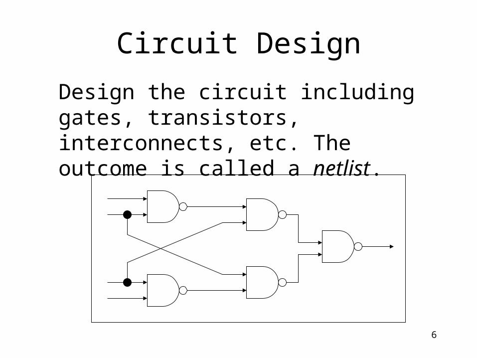
Circuit Design
Design the circuit including gates, transistors, interconnects, etc. The outcome is called a netlist.

7
Physical Design
Convert the netlist into a geometric representation. The outcome is called a layout.
8
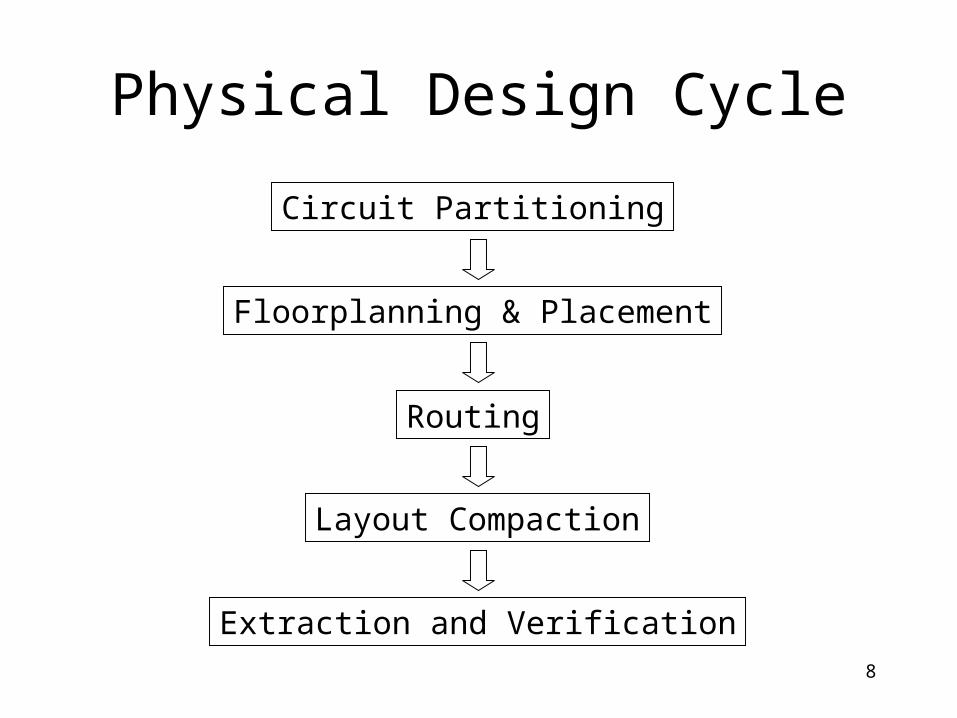
Physical Design Cycle
Circuit Partitioning
Floorplanning & Placement
Routing
Layout Compaction
Extraction and Verification
9
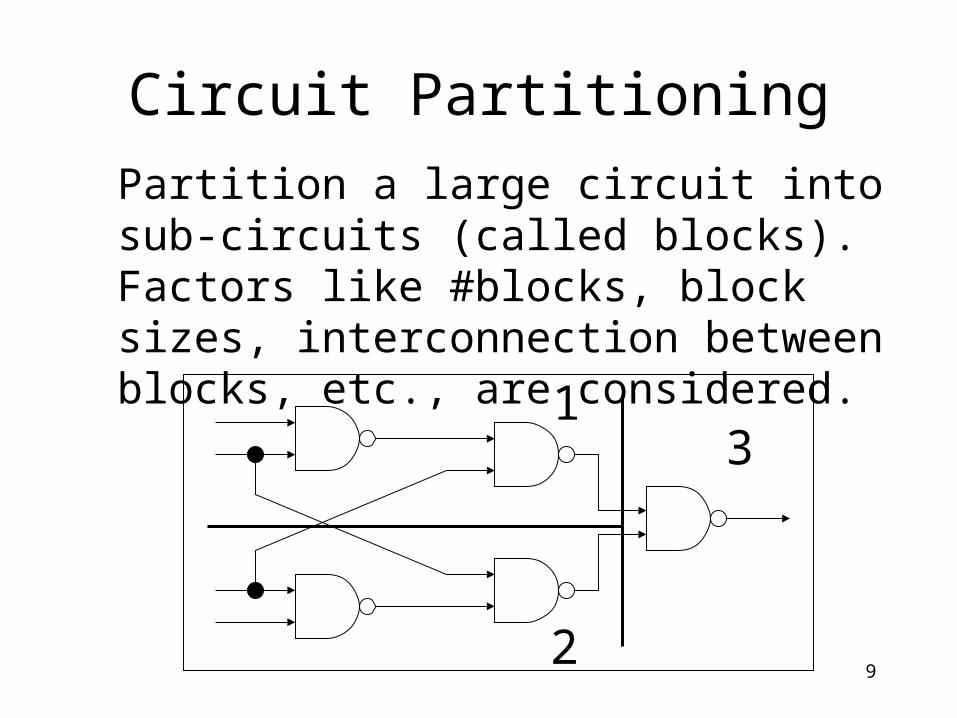
Circuit Partitioning
Partition a large circuit into sub-circuits (called blocks). Factors like #blocks, block sizes, interconnection between blocks, etc., are considered.
1
2
3
10
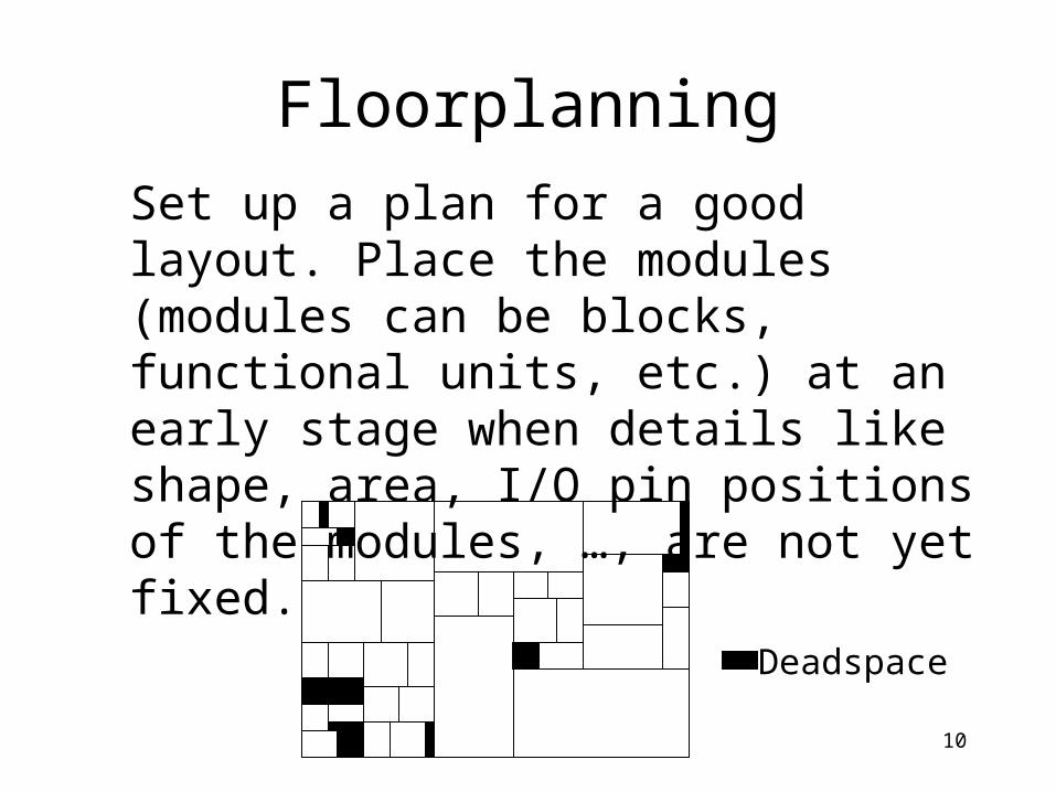
Floorplanning
Set up a plan for a good layout. Place the modules (modules can be blocks, functional units, etc.) at an early stage when details like shape, area, I/O pin positions of the modules, …, are not yet fixed.
Deadspace

11
Placement Exact placement of the modules (modules
can be gates, standard cells, etc.) when details of the module design are known. The goal is to minimize the delay, total area and interconnect cost.
v
Feedthrough
Standard cell type 1
Standard cell type 2

12
Routing
Complete the interconnections between modules. Factors like critical path, clock skew, wire spacing, etc., are considered. Include global routing and detailed routing.
v
Feedthrough
Type 1 standard cel1
Type 2 standard cell
13
Compaction & Verification
• Compaction is to compress the layout from all directions to minimize the total chip area.
• Verification is to check the correctness of the layout. Include DRC (Design Rule Checking), circuit extraction (generate a circuit from the layout to compare with the original netlist), performance verification (extract geometric information to compute resistance, capacitance, delay, etc.)
14
Design Styles
• Full-Custom Design
• Standard Cell Design
• Gate Array Design
• Field Programmable Gate Array Design (FPGA)

15
Full-Custom Design
• No rigid restrictions on layout.
• More compact design.
• Longer design time.
• Hierarchical: chip clusters units functional units.

16
Full Custom Design
17
Standard Cell Design
• Rectangular cells of the same height.
• Cell library (has 500 - 1200 cells).
• Cells placed in rows and space between rolls are called channels for routing.
• Feedthroughs

18
Standard Cell Design

19
Gate Array Design
• Each chip is prefabricated with an array of identical gates or cells.
• The chip is “customized” by fabricating routing layers on top.

20
An Uncommitted Gate Array

21
A Committed Gate Array

22
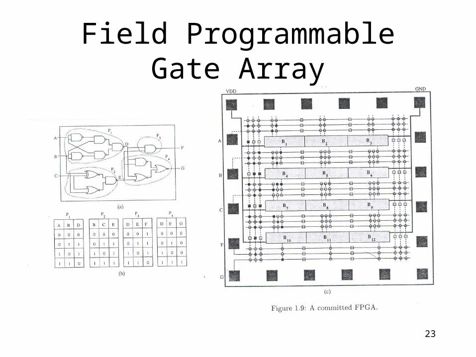
Field Programmable Gate Array
• Chips are prefabricated with logic blocks and interconnects.
• Logic and interconnects can be programmed (erased and re-programmed) by users. No fabrication is needed.
• Interconnects are predefined wire segments of fixed lengths with switches in between.
23
Field Programmable Gate Array

24
Trends in VLSI
• Transistor– Smaller, faster, use less power
• Interconnect– Less resistive, faster, longer (denser design)
• Huge power consumption and heat dissipation• Noise and cross talk.

25
Interconnect Delay
0.651989
0.51992
0.351995
0.251998
0.182001
0.132004
0.12007
0
5
10
15
20
25
30
35
40
Gate delayInterconnect delay
Source: SIA Roadmap 1997

26
Chip Area
micron

27
Processor Performance
0.1
1
10
100
1,000
10,000
100,000
1000,000
75 80 85 90 95 00 05 10 15
MIPS
Source: Intel
808680286
80386 Processor80486 Processor
Pentium ProcessorPentium Pro Processor
100,000 MIPS
28
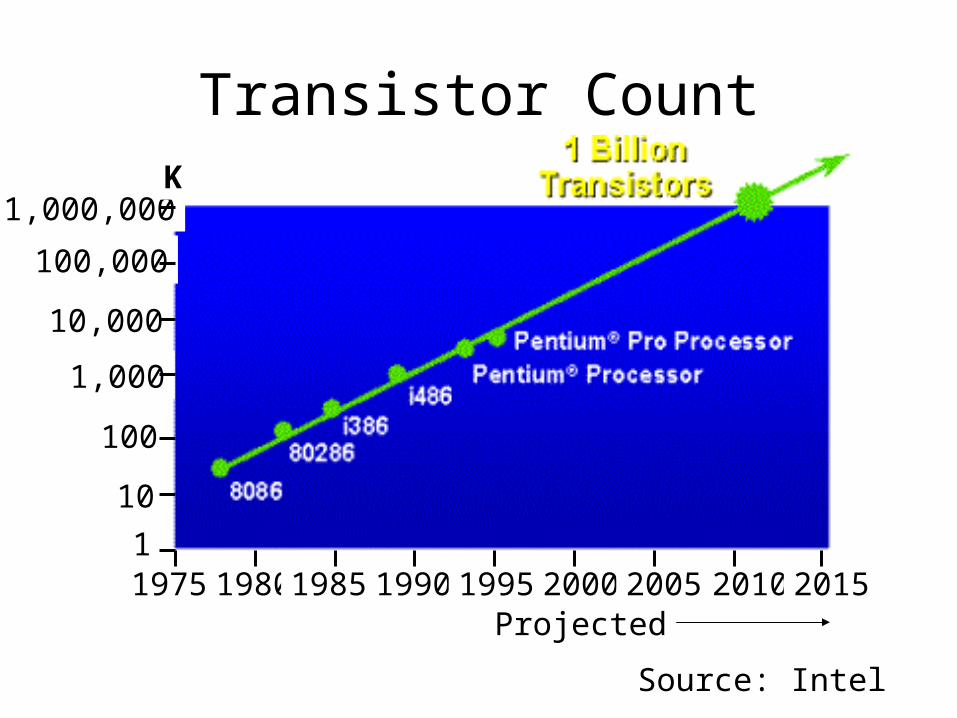
Transistor Count
1975 1980 1985 1990 1995 2000 2005 2010 20151
10
100
1,000
10,000
100,000
1,000,000K
Source: Intel
Projected
29
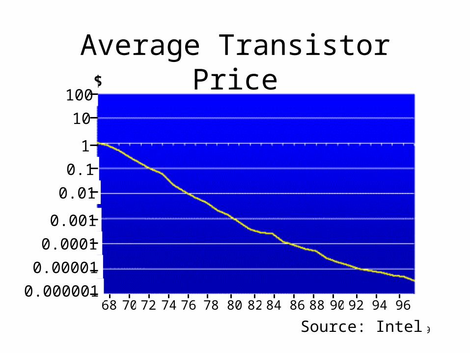
Average Transistor Price
68 70 72 74 76 78 80 82 84 86 88 90 92 94 96
$
0.000001
0.00001
0.0001
0.001
0.01
0.1
1
10
100
Source: Intel
30
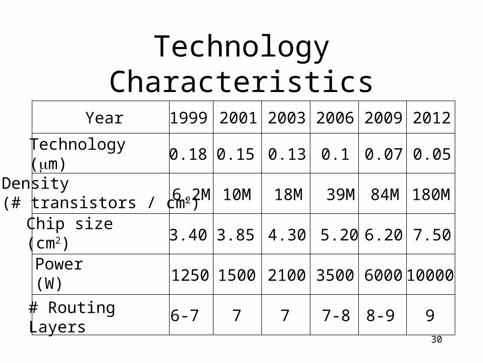
Technology Characteristics
Year 1999 2001 2003 2006 2009 2012
Technology(m)Density(# transistors / cm2)Chip size(cm2)Power(W)
# RoutingLayers
0.18 0.15 0.13 0.1 0.07 0.05
6.2M 10M 18M 39M 84M 180M
3.40 3.85 4.30 5.20 6.20 7.50
1250 1500 2100 3500 6000 10000
6-7 7 7 7-8 8-9 9
31
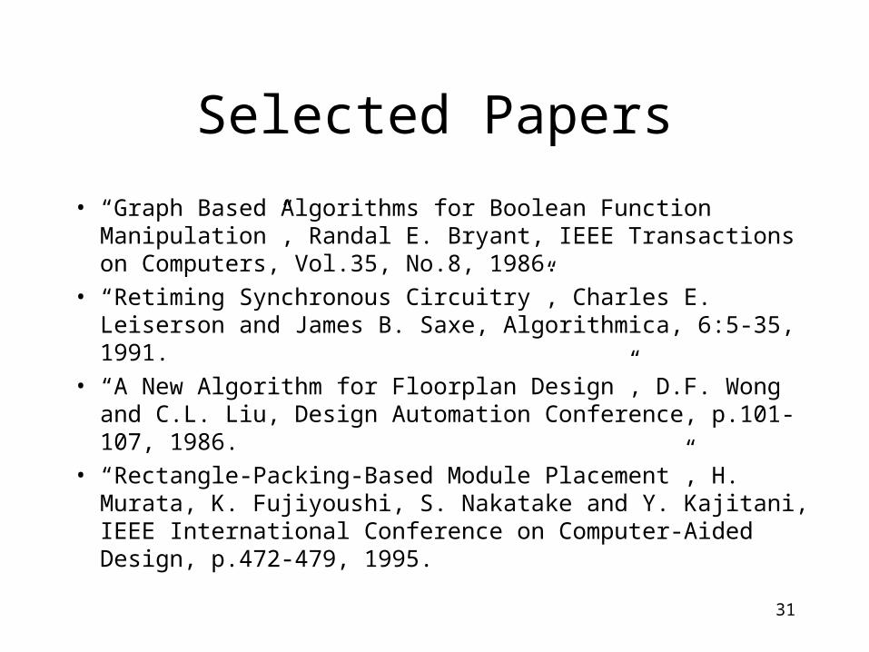
Selected Papers
• “Graph Based Algorithms for Boolean Function Manipulation”, Randal E. Bryant, IEEE Transactions on Computers, Vol.35, No.8, 1986.
• “Retiming Synchronous Circuitry”, Charles E. Leiserson and James B. Saxe, Algorithmica, 6:5-35, 1991.
• “A New Algorithm for Floorplan Design”, D.F. Wong and C.L. Liu, Design Automation Conference, p.101-107, 1986.
• “Rectangle-Packing-Based Module Placement”, H. Murata, K. Fujiyoushi, S. Nakatake and Y. Kajitani, IEEE International Conference on Computer-Aided Design, p.472-479, 1995.

32
Selected Papers
• “A linear time heuristic for improving network partitions”, Fiduccia and Mattheyses, Design Automation Conference, 1982.
• “Efficient Network Flow Based Min-Cut Balance Partitioning”, Hannah H. Yang and D.F. Wong, International Conference on Computer-Aided Design, pp.50-55, 1994.
• “Multilevel k-way Hypergraph Partitioning”, G. Karypis and V. Kumar, Design Automation Conference, pp.344-347, 1999.

33
Selected Papers
• “An Optimal Technology Mapping Algorithm for Delay Optimization in Lookup-Table Based FPGA Designs”, Jason Cong and Yuzheng Ding, International Conference on Computer-Aided Design, 1992.
• “The Timberwolf Placement and Routing Package”, C. Sechen and A.L. Sangiovanni-Vincentelli, IEEE Journal of Solid-State Circuits, 20:510-522, 1985.
• “Gordian: A New Global Optimization/Rectangle Dissection Method for Cell Placement”, J. Kleinhans, G. Sigl and F. Johannes, International Conference on Computer-Aided Design, 1994.

34
Floorplanning

35
Floorplanning The floorplanning problem is to plan the
positions and shapes of the modules at the beginning of the design cycle to optimize the circuit performance:– Chip area
– Total wirelength
– Delay of critical path
– Routability
– Others, e.g., noise, heat dissipation, etc.

36
Floorplanning Problem
• Input:– n Blocks with areas A1, ... , An
– Bounds ri and si on the aspect ratio of block Bi
• Output:– Coordinates (xi, yi), width wi and height hi for each
block such that hi wi = Ai and ri hi/wi si
• Objective:– To optimize the circuit performance.

37
Simulated Annealing Approach
• Many floorplanning tools are based on simulated annealing approach.
• In simulated annealing, we need to have a good representation for each candidate floorplan solution.
• There are three kinds of floorplan: slicing, mosaic and non-slicing.

38
P-admissible Representation
A packing representation is P-admissible if:– The solution space is finite.– Every solution corresponds to a feasible packing.– Evaluation for each solution, i.e., computing the cos
t value, is possible in polynomial time, and so is the realization of the corresponding packing.
– The optimal packing is included in the solution space and corresponds to the one with the best evaluated cost value.
39
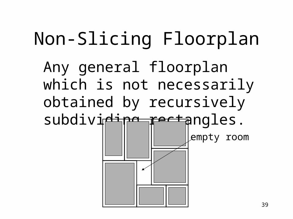
Non-Slicing Floorplan
Any general floorplan which is not necessarily obtained by recursively subdividing rectangles.
empty room
40
Slicing Floorplan Representation
““A New Algorithm for Floorplan Design”, D.F. A New Algorithm for Floorplan Design”, D.F. Wong and C.L. Liu, Design Automation Wong and C.L. Liu, Design Automation Conference, pp.101-107, 1986.Conference, pp.101-107, 1986.
41
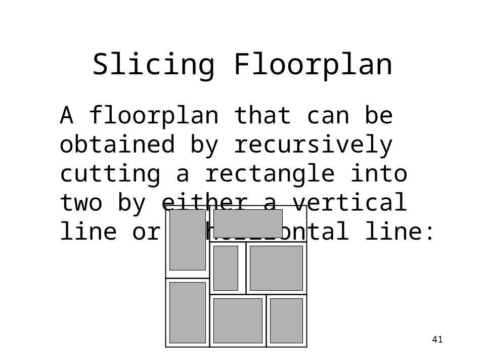
Slicing Floorplan
A floorplan that can be obtained by recursively cutting a rectangle into two by either a vertical line or a horizontal line:
42
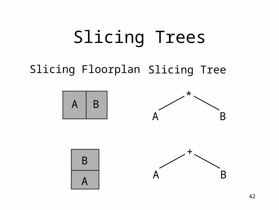
Slicing Trees
Slicing Floorplan
*
A B
Slicing Tree
B
A
+
A B
A B

43
Slicing Trees
62
3
54
7
1
Slicing Floorplan*
+ +
2 1 3+
*
6 4
*
7 5
Slicing Tree
Polish Expression(postorder traversal of slicing tree)
21+67*45*+3+*

44
Normalized PE
A normalized Polish Expression has no consecutive + or *.
62
3
54
7
1
Slicing Floorplan
Polish Expression
*
+ +
2 1 +*
6 *7 3
Slicing Tree
4 5
21+67*45*3++*
45
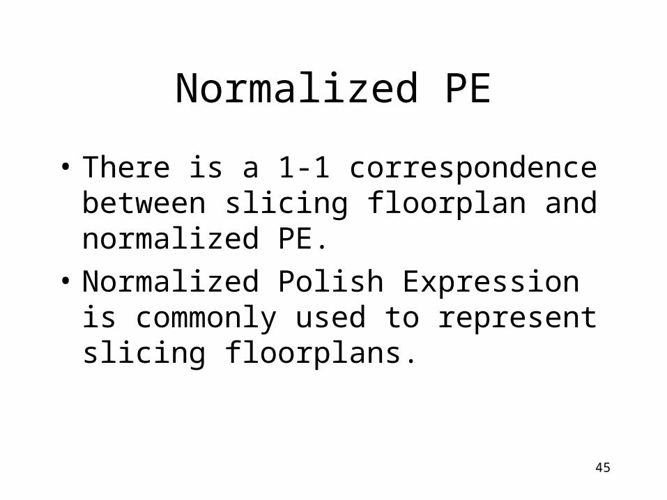
Normalized PE
• There is a 1-1 correspondence between slicing floorplan and normalized PE.
• Normalized Polish Expression is commonly used to represent slicing floorplans.
46
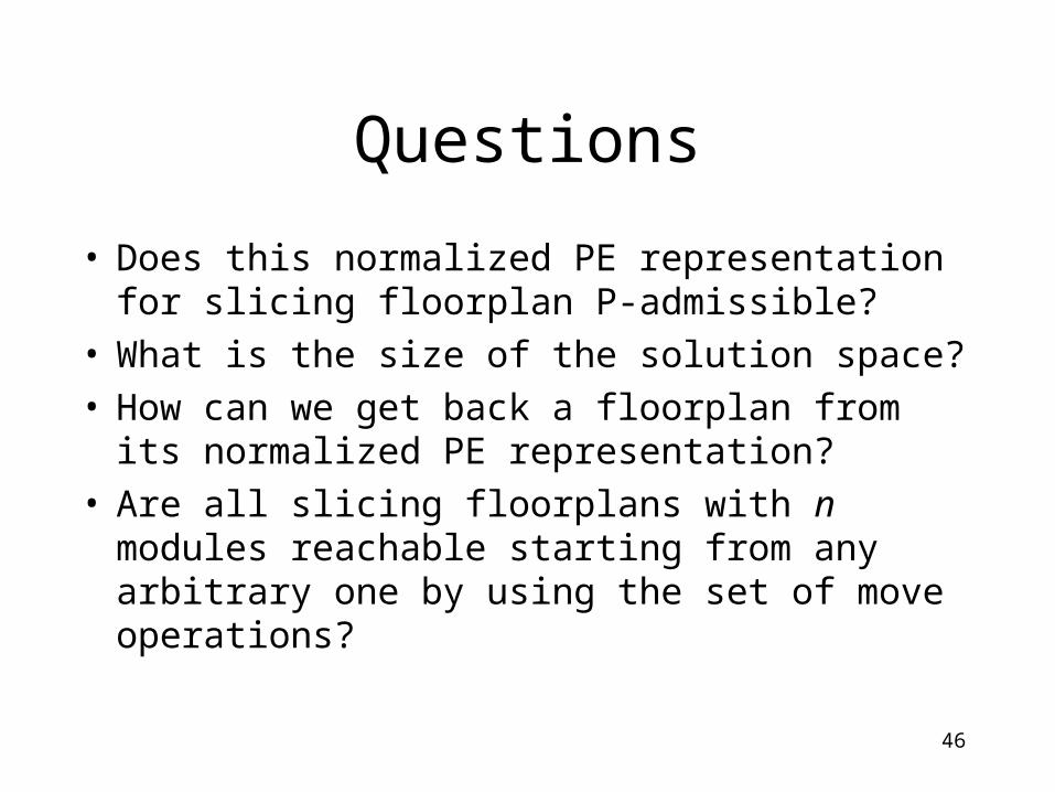
Questions
• Does this normalized PE representation for slicing floorplan P-admissible?
• What is the size of the solution space?• How can we get back a floorplan from its
normalized PE representation?• Are all slicing floorplans with n modules reachable
starting from any arbitrary one by using the set of move operations?
47
Shaping
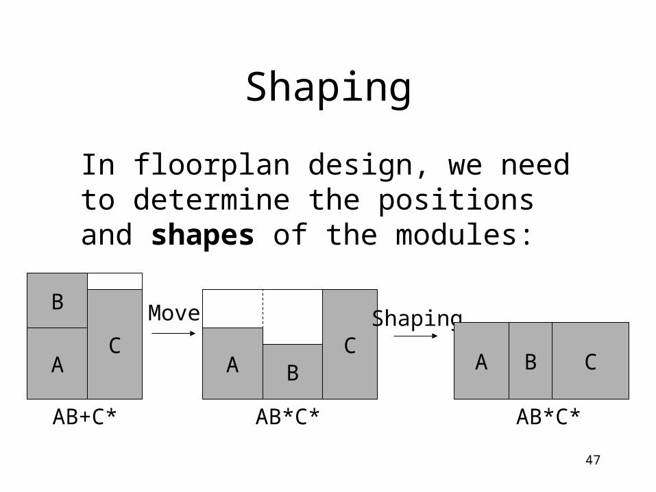
In floorplan design, we need to determine the positions and shapes of the modules:
B
AC
AB+C*
Move
C
AB*C*
Shaping
A B CBA
AB*C*

48
Shaping in Slicing Floorplan
• Shaping in slicing floorplan can be done by “shape curve computation”.
• Given a Polish expression of n modules and the areas of the modules, how to determine their dimensions to minimize the total area of the floorplan?
49
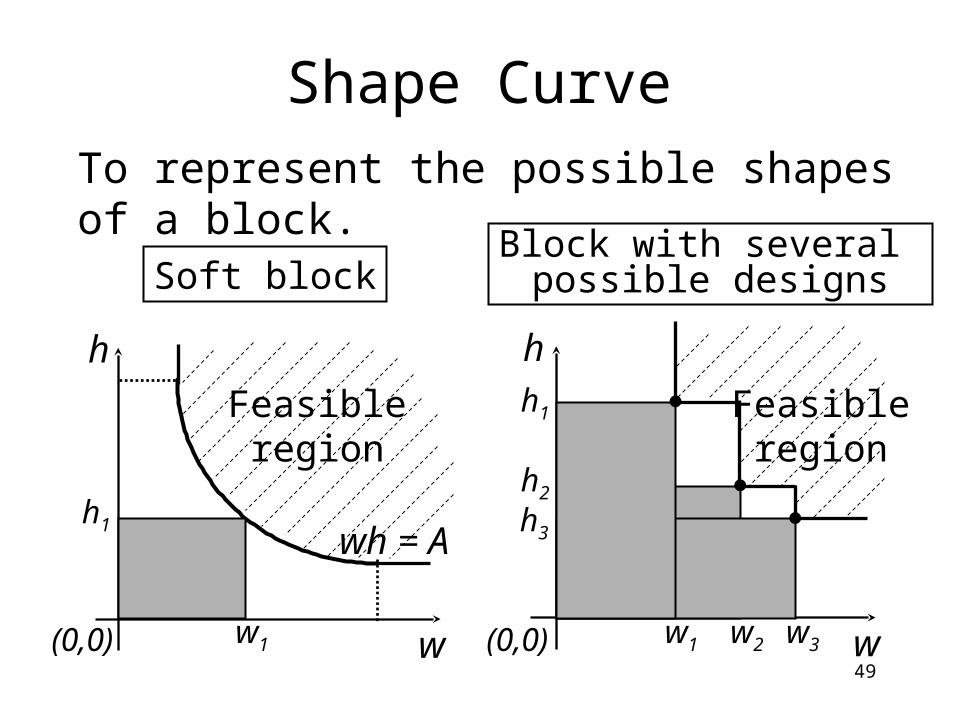
Shape Curve To represent the possible shapes of a block.
w
h
(0,0)
wh = A
Soft blockBlock with several possible designs
w
h
(0,0)
Feasibleregion
Feasibleregion
w1
h1
w1 w2 w3
h3
h2
h1
50
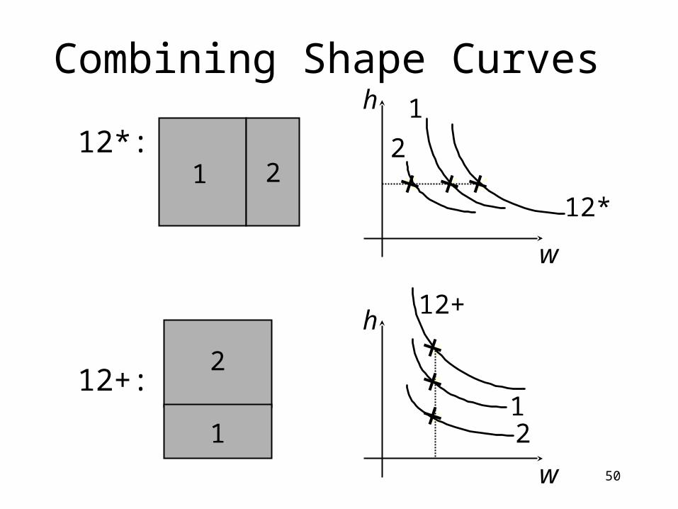
Combining Shape Curves
12*:
12+:
1 2
h
w
12*
1
2
2
1
w
h
21
12+
51
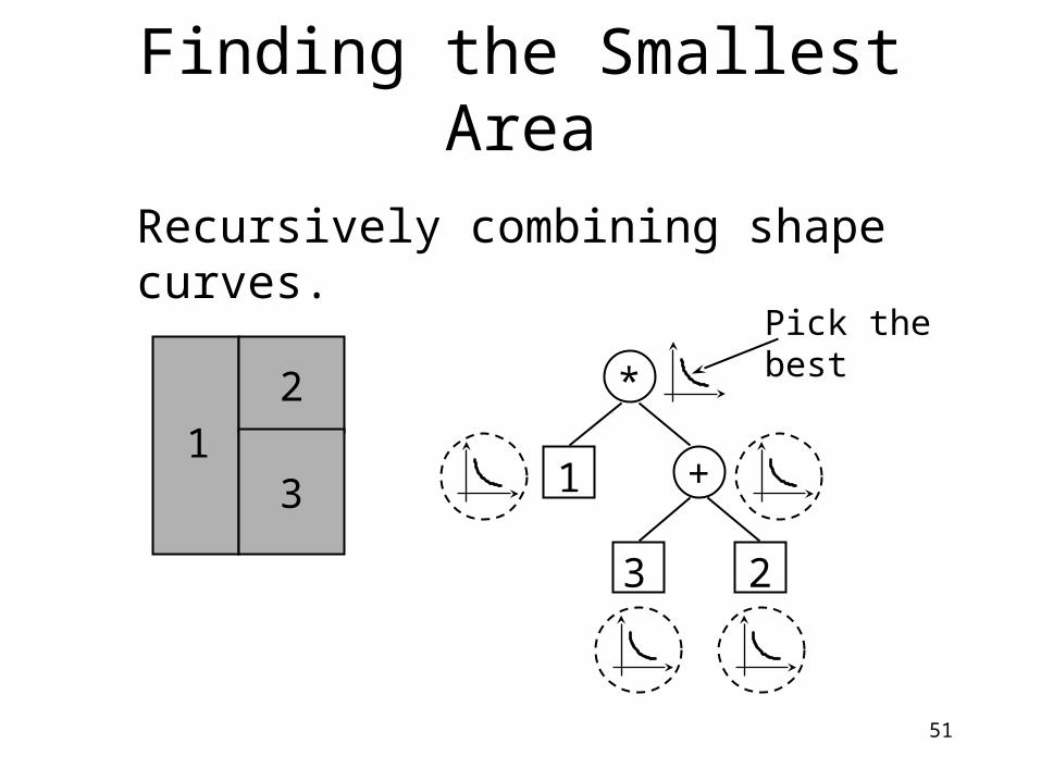
Finding the Smallest Area
Recursively combining shape curves.
*
23
Pick thebest
1
2
31
+
52
Updating Shape Curves
• If each shape curve has k points, the shape curve computational time for each normalized PE is O(kn).
• After each move, there are only small changes in the floorplan, so no need to compute all the shape curves from scratch again.
• We can update shape curves incrementally after each move. Expected run time is O(k log n).

53
Non-Slicing Floorplan Representation
“Rectangle-Packing-Based Module Placement”, H. Murata, K. Fujiyoushi, S. Nakatake and Y. Kajitani, IEEE International Conference on Computer-Aided Design, 1995, pages 472-479.
54
Sequence Pair (SP)
A floorplan is represented by a pair of permutations of the module names:
e.g. 1 3 2 4 5 3 5 4 1 2
A sequence pair (s1, s2) of n modules can represent all possible floorplans formed by the n modules by specifying the pair-wise relationship between the modules.
55
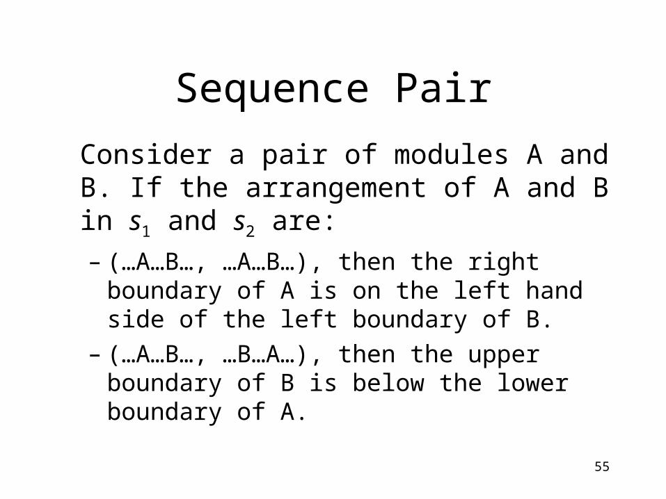
Sequence Pair
Consider a pair of modules A and B. If the arrangement of A and B in s1 and s2 are:
– (…A…B…, …A…B…), then the right boundary of A is on the left hand side of the left boundary of B.
– (…A…B…, …B…A…), then the upper boundary of B is below the lower boundary of A.

56
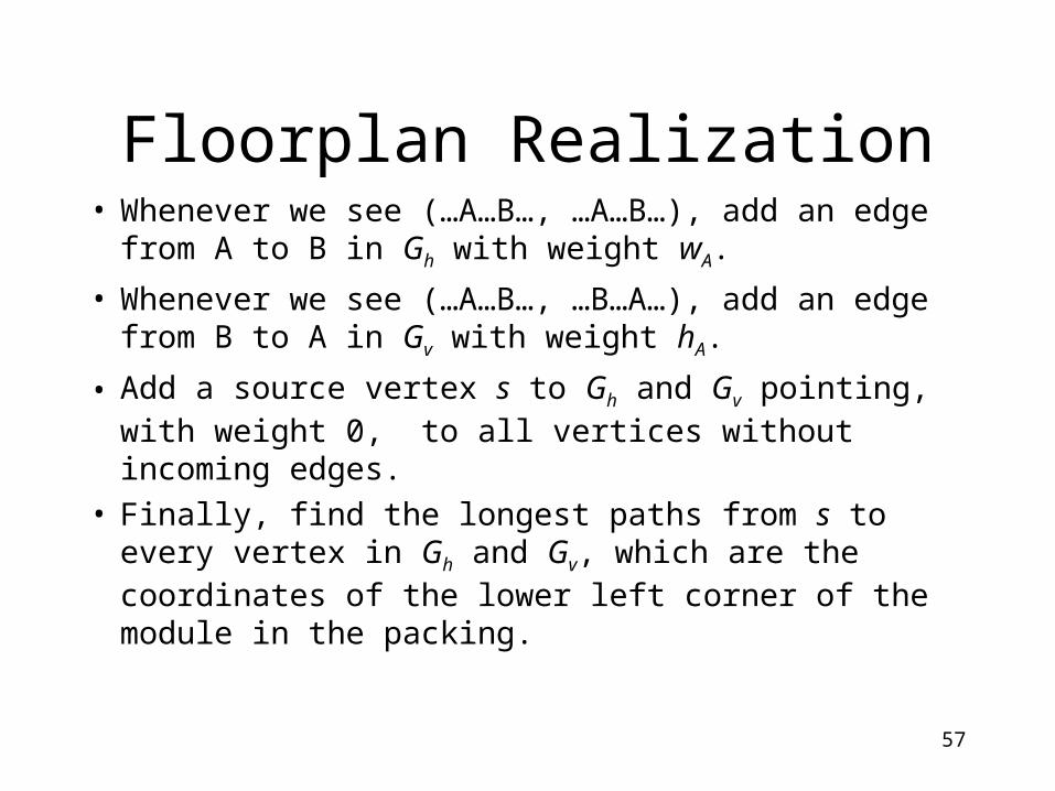
Floorplan Realization
• Floorplan realization is the step to construct a floorplan from its representation.
• To construct a floorplan from a sequence pair, we can make use of the horizontal and vertical constraint graphs (Gh and Gv).
57
Floorplan Realization• Whenever we see (…A…B…, …A…B…), add an
edge from A to B in Gh with weight wA.
• Whenever we see (…A…B…, …B…A…), add an edge from B to A in Gv with weight hA.
• Add a source vertex s to Gh and Gv pointing, with weight 0, to all vertices without incoming edges.
• Finally, find the longest paths from s to every vertex in Gh and Gv, which are the coordinates of the lower left corner of the module in the packing.

58
Example
2
54
1 3
(13245,41352 )
2
1.2
1
1.1 1
1.2
2
2.4 1.2
1
3 2
5
4
1.21.2
1.2
1.1
1.1
2.4s
0
0
Gh
1
3 2
5
4s
0 0
Gv
11 1
2
59
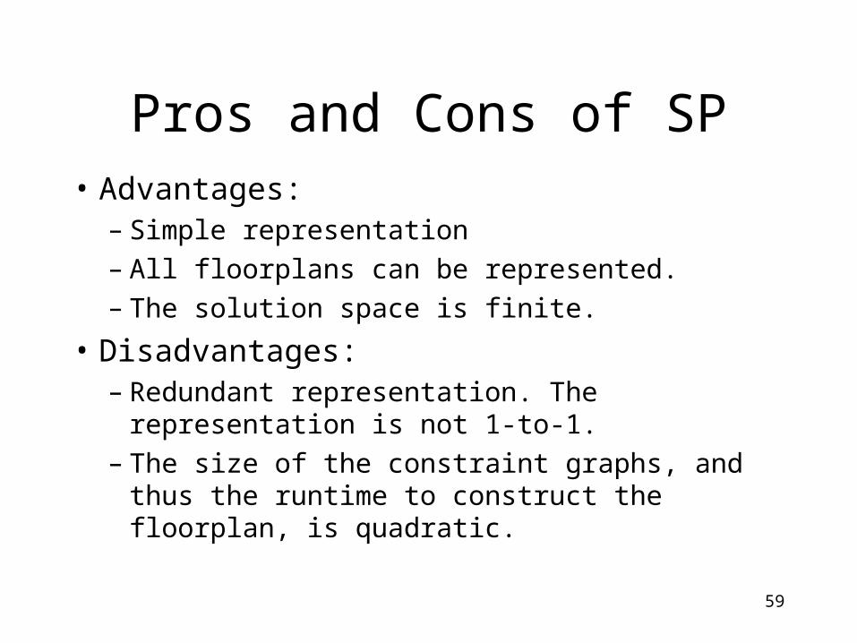
Pros and Cons of SP• Advantages:
– Simple representation– All floorplans can be represented.– The solution space is finite.
• Disadvantages:– Redundant representation. The representation is not
1-to-1.– The size of the constraint graphs, and thus the
runtime to construct the floorplan, is quadratic.

60
Questions
• Is the SP representation for general non-slicing floorplan P-admissible?
• Can we improve the runtime to realize a floorplan from its SP representation? (“FAST-SP: A Fast Algorithm for Block Placement on Sequence Pair”, X. Tang and D.F. Wong, ASP-DAC 2001, pp. 521-526.)
Top Related