


Languages
Pages
Legal

Substrates and Epitaxy in III-V Manufacturing
Robert Yanka2010 CS MANTECH Workshop

2010 CS MANTECH Workshop Session 2 2
Overview
• Substrate Manufacturing Overview
• Metal-Organic Chemical Vapor Deposition (MOCVD) Basics
• Molecular Beam Epitaxy (MBE) Basics
• Epiwafer Characterization
• RFMD Epiwafer Production Overview

2010 CS MANTECH Workshop Session 2 3
Substrate Manufacturing Overview
2010 CS MANTECH Workshop Session 2 4
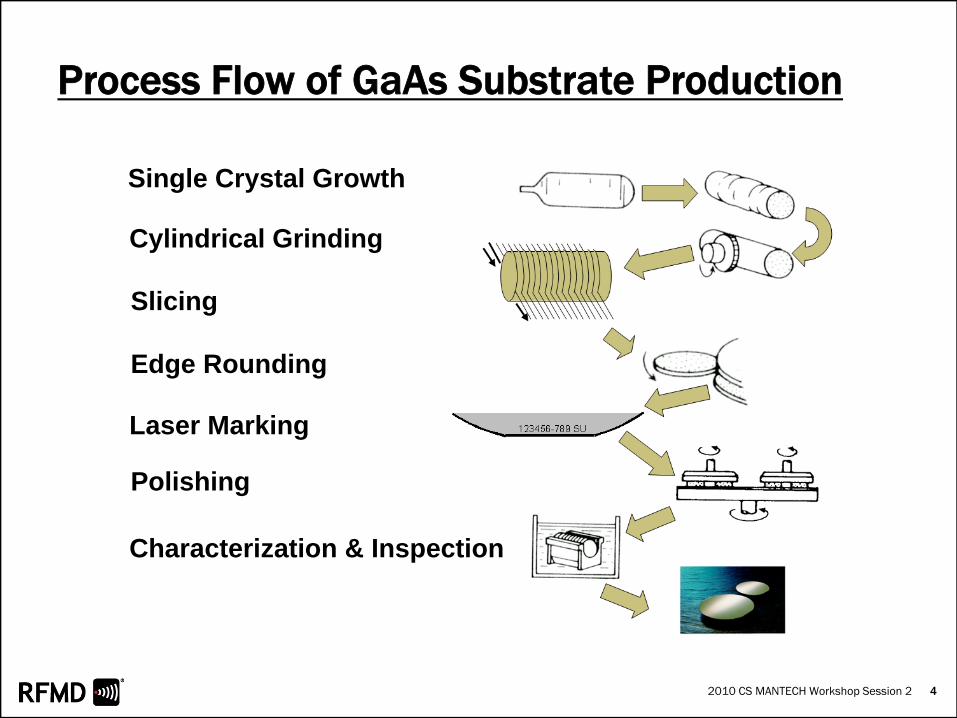
Process Flow of GaAs Substrate Production
Single Crystal Growth
Cylindrical Grinding
Slicing
Edge Rounding
Polishing
Characterization & Inspection
Laser Marking

2010 CS MANTECH Workshop Session 2 5
Substrates – Boule Growth Techniques
As
As
Growing
Cooling
SolidLiquid
Solid
Temperature Profile low
Melting Point
Seed
Seed
Czochralski (Cz) Growth Horizontal Bridgman (HB) Growth

2010 CS MANTECH Workshop Session 2 6
Substrates – LEC vs. Vertical Boat
Vertical BoatLiquid EncapsulatedCzochralski (LEC)
Boule Moves Furnace Moves

2010 CS MANTECH Workshop Session 2 7
Substrate – VB vs. VGF
Longer Ingot
Shorter Ingot
Vertical Boat vs. Vertical Gradient Freeze

2010 CS MANTECH Workshop Session 2 8
Substrates – Grinding and Slicing
As sliced Wafers
Wire Saw

2010 CS MANTECH Workshop Session 2 9
Substrates – Edge Beveling and Polishing
Laser Marking
Double-Side Polishing
Edge Beveling
2010 CS MANTECH Workshop Session 2 10
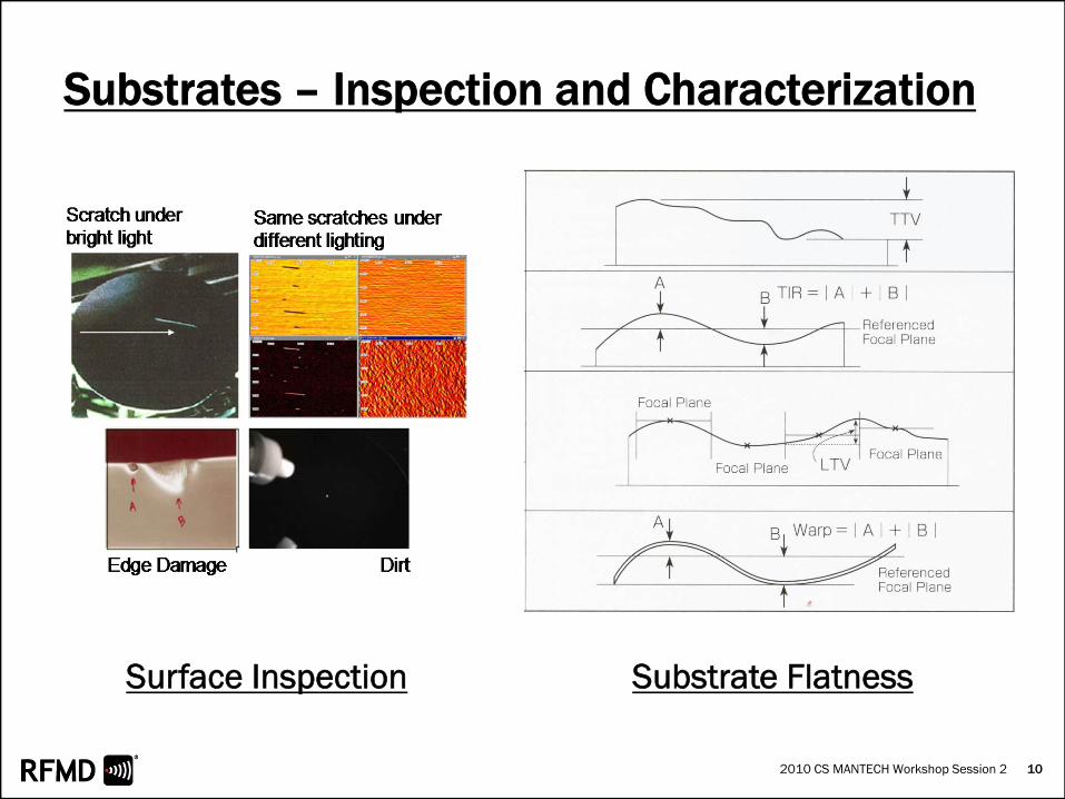
Substrates – Inspection and Characterization
Surface Inspection Substrate Flatness

2010 CS MANTECH Workshop Session 2 11
Substrates – Inspection and Characterization
• Electrical Characterization– Hall and non-contact resistivity measurements are
performed on the seed and tail to determine the electrical characteristics of the boule
• Etch Pit Decoration (KOH)– Chemical etch used to
determine dislocation density

2010 CS MANTECH Workshop Session 2 12
MOCVD Basics

2010 CS MANTECH Workshop Session 2 13
Epitaxial Crystal Growth
• Epitaxy – is derived from the Greek word meaning “ordered upon”– Epitaxy is the growth of thin single crystals of one material on the
crystal face of the same (homoepitaxy) or another (heteroepitaxy) material, such that the two materials have a defined, relative structural orientation
• Two main Rules of epitaxy– Matching of Symmetry between the substrate and the epilayer– Misfit between lattice constants of substrate and epilayer should be
minimal
• Examples of Epitaxy:-– GaAs on GaAs (Homoepitaxy) (misfit value = 0)– AlGaAs on GaAs (Heteroepitaxy) (misfit value > 0)– InGaAs on GaAs (Heteroepitaxy) (misfit value >> 0)

2010 CS MANTECH Workshop Session 2 14
Metal Organic Chemical Vapor Deposition
• First documented in 1963 by Harold Manasevit for silicon on sapphire at Rockwell Corporation
• Manasevit grew GaAs on sapphire in 1968
• Growth involves the transport of metal-organic and hydride precursors to heated substrates where they pyrolize, leaving the growth species on the substrate surface
• Also referred to as (LP-, AP-) OMCVD, MOVPE, OMVPE
2010 CS MANTECH Workshop Session 2 15
Metal Organic Chemical Vapor Deposition
• MOCVD is capable of high growth rates, making it the most widely used technique for the manufacture of optical devices such as LED’s
• At lower growth rates, MOCVD can produce abrupt interfaces, allowing it’s application to RF devices such as HBT’s and FET’s
2010 CS MANTECH Workshop Session 2 16
Metal Organic Chemical Vapor Deposition
• Source materials for MOCVD are extremely hazardous, requiring rigorous monitoring and handling procedures– Metal-organics are toxic and pyrophoric– Hydrides are highly toxic– Hydrogen carrier gas is explosive
• Maintenance cycles driven by coating of reaction chamber– Requires relatively frequent cleaning to remove material from
system components and reduce particulates in the chamber– System downtime is on the order of hours

2010 CS MANTECH Workshop Session 2 17
MOCVD – System Block Diagram

2010 CS MANTECH Workshop Session 2 18
MOCVD – System Photograph

2010 CS MANTECH Workshop Session 2 19
MOCVD – System Schematic

2010 CS MANTECH Workshop Session 2 20
MOCVD – Flow Control
• Mass Flow Controller (MFC)– A portion of the gas flow passes through a tube incorporating two
temperature sensors– A temperature difference results that is proportional to the mass
flow through the controller

2010 CS MANTECH Workshop Session 2 21
MOCVD – Sources
MO BubblerCarrier gas (H2) flowing through the bubbler picks up MO vapor from the liquid
Typical MOCVD SourcesGroup III: Tri-methyl gallium, Tri-methyl aluminum, Tri-methyl indiumGroup V: Arsine, Phosphine, Ammonia, Tertiary-butyl arsine (TBAs),
Tertiary-butyl phosphine (TBP)Dopants: Carbon-tetrabromide, Disilane, Di-methyl zinc

2010 CS MANTECH Workshop Session 2 22
TMGa
δ0
H2V
Diffusion
CH3 radical
AsH3
J
MOCVD - Growth Dynamics
• Source molecules mixed into a carrier gas (hydrogen) with mid-stream velocity V• Friction reduces gas velocity to near zero at surfaces • Sources must diffuse through the near stagnant boundary layer above substrate • Precursor decomposition• Surface adsorption & diffusion incorporation and growth • Growth rate depends upon pressure, flow rate and temperature

2010 CS MANTECH Workshop Session 2 23
MOCVD – Growth Regimes
A. Desorption / Gas Phase Limited Growth
B. Mass Transport Limited Growth (Diffusion through boundary layer).
C. Surface Kinetic Limited Growth
Growth rate ~ temperature independent in mass transport limited regime

2010 CS MANTECH Workshop Session 2 24
MOCVD – Growth Rate Control
Growth Rate: The Mass Transport Limited Regime

2010 CS MANTECH Workshop Session 2 25
MOCVD – In-situ Monitoring
• Pyrometry– Substrate temperature measurement– Multi-wavelength for emissivity correction
• Reflectometry– Growth rate and ternary composition data– Wafer curvature measurement
Transparent Film Absorbing Film
2010 CS MANTECH Workshop Session 2 26
MBE Basics

2010 CS MANTECH Workshop Session 2 27
Molecular Beam Epitaxy
• Molecular Beam Epitaxy was developed by Alfred Cho and John Arthur in 1970 at Bell Labs
• Originally applied to the growth of GaAs lasers
• Growth involves the evaporation of high purity elemental sources in an ultra-high vacuum environment
• The resulting “molecular beams” impinge heated substrates producing epitaxial growth

2010 CS MANTECH Workshop Session 2 28
Molecular Beam Epitaxy
• MBE typically utilizes slower growth rates (~1µm/hr) resulting in high quality, atomically abrupt interfaces. This is an advantage for superlattice and/or quantum well based applications.
• Relatively simple growth kinetics and precise layer control have made MBE a popular technique for investigating novel devices structures in R&D. However, MBE is also widely used in the manufacture of pHEMT’s and HBT’s.
• MBE source materials are relatively safe, as they are low vapor pressure solids at room temperature

2010 CS MANTECH Workshop Session 2 29
Molecular Beam Epitaxy
• Maintenance cycles are driven by the need to replenish sources
• Ultra-high vacuum environment requires extensive cleaning and baking of the system– Maintenance cycles require several weeks to complete
• Campaign lengths between cleaning can range from six to nine months

2010 CS MANTECH Workshop Session 2 30
MBE – Block Diagram
Wafers are introduced from atmosphere into the load lock.
Next they move into the prep chamber for outgassing.
Finally, they are transferred into the deposition chamber for growth.

2010 CS MANTECH Workshop Session 2 31
MBE - System Photograph
Load Locks
Prep/Transfer Chamber Depo Chamber
Source Flange
Cryo Pumps
Veeco Gen2000

2010 CS MANTECH Workshop Session 2 32
MBE – System Schematic
Cryopanel maintains low impurity background in the depo chamber.
Substrate rotation improves uniformity.
2010 CS MANTECH Workshop Session 2 33
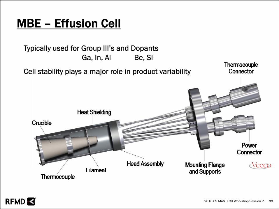
MBE – Effusion Cell
Typically used for Group III’s and DopantsGa, In, Al Be, Si
Cell stability plays a major role in product variability

2010 CS MANTECH Workshop Session 2 34
MBE – Valved Cracker
Cracking Zone
Sublimator(Source Load)
Valve Actuator
Group V’s consumed at a high rate due to the flux requirements
Temperature ramps are impractical for the large material loads required
Valved cells provide flux control at a constant temperture
Valve controls flow betweensublimator and cracking zone
2010 CS MANTECH Workshop Session 2 35
MBE – Growth Dynamics
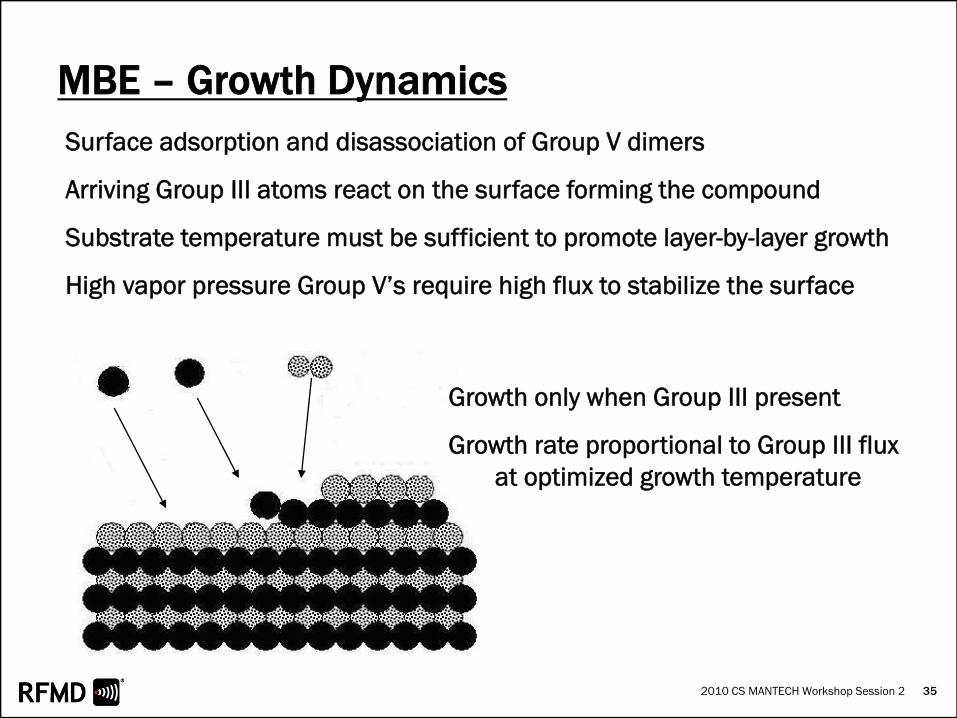
Growth only when Group III present
Growth rate proportional to Group III fluxat optimized growth temperature
Surface adsorption and disassociation of Group V dimers
Arriving Group III atoms react on the surface forming the compound
Substrate temperature must be sufficient to promote layer-by-layer growth
High vapor pressure Group V’s require high flux to stabilize the surface

2010 CS MANTECH Workshop Session 2 36
MBE – Growth Rate
• Growth rate proportional to Group III flux– Follows Arrhenius relationship– Doping is controlled in the same manner as growth rate

2010 CS MANTECH Workshop Session 2 37
MBE – In-situ Monitoring
• Ion gauge for measuring source material flux
• Reflection High Energy Electron Diffraction (RHEED) for growth rate and structural information
• Optical pyrometry for substrate temperature
• Band edge thermometry for substrate temperature
• Laser reflectometry for growth rate
• Atomic absorption flux monitoring

2010 CS MANTECH Workshop Session 2 38
Epiwafer Characterization
2010 CS MANTECH Workshop Session 2 39
Epiwafer Characterization
• Characterization Categories– Surface morphology– Electrical properties– Structural properties
• Destructive vs. Non-Destructive
• Product Wafers vs. Process Monitors
2010 CS MANTECH Workshop Session 2 40
Epiwafer Characterization – Surface MorphologySurface roughness, particulates, growth defects, scratchesTypically non-destructive
• Visual Inspection– Looking for gross defects such as haze, scratches, large particles
• Automated Inspection– Commercial tools such as Tencor’s SurfScan or Candela– Provides wafers maps for haze, point defects and scratches
• Optical Microscopy– Standard and phase-contrast– Usually for diagnostic purposes, to indentify the type of defects
2010 CS MANTECH Workshop Session 2 41
Epiwafer Characterization – Electrical PropertiesDoping levels, doping uniformity, doping depth profile
Carrier concentration, mobility, sheet resistance
Destructive or non-destructive depending upon technique
• Electro-chemical CV Profiling– Usually referred to as Polaron from the commercial system– Provides a carrier concentration depth profile but is destructive
• Hall Measurement– Provides average carrier concentration and mobility over a sample– Typically destructive (non-destructive approaches exist)
• Non-contact Sheet Resistance– Provides non-destructive sheet resistance mapping

2010 CS MANTECH Workshop Session 2 42
Epiwafer Characterization – Structural PropertiesLayer thickness, composition, uniformity and crystal qualityTechniques are typically non-destructive
• Surface Profilometry– Simple step height measurement for thickness / growth rate
• X-ray Diffraction / Reflection– Layer thickness and composition mapping– Defect density estimates
• Photoluminescence– Optical technique for probing bandgap– Provides composition mapping and material quality data
2010 CS MANTECH Workshop Session 2 43
RFMD Epiwafer Production Overview

2010 CS MANTECH Workshop Session 2 44
RFMD MBE Operations• Nearly 100% of AlGaAs HBT and pHEMT starts are from
MBE systems in Greensboro, NC
• Minimal number of device structures– Easily more MBE systems than SKU’s– Allows an MBE tool to produce a single SKU for weeks or months
• Heavy focus on production metrics– System uptime, throughput and yield– Manpower efficiency– Reproducibility across different types of MBE systems– Wafer uniformity and run-to-run reproducibility
2010 CS MANTECH Workshop Session 2 45
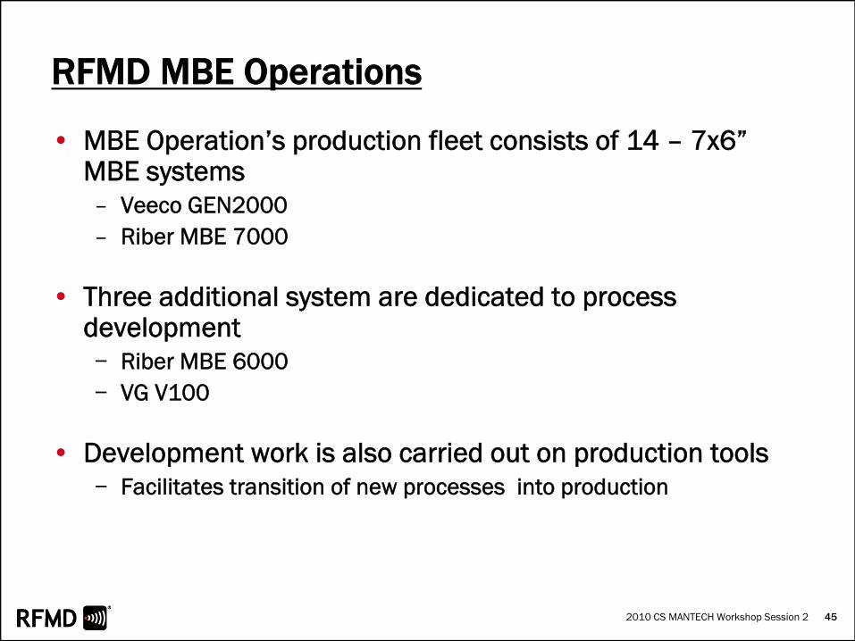
RFMD MBE Operations
• MBE Operation’s production fleet consists of 14 – 7x6” MBE systems– Veeco GEN2000– Riber MBE 7000
• Three additional system are dedicated to process development− Riber MBE 6000− VG V100
• Development work is also carried out on production tools− Facilitates transition of new processes into production
2010 CS MANTECH Workshop Session 2 46
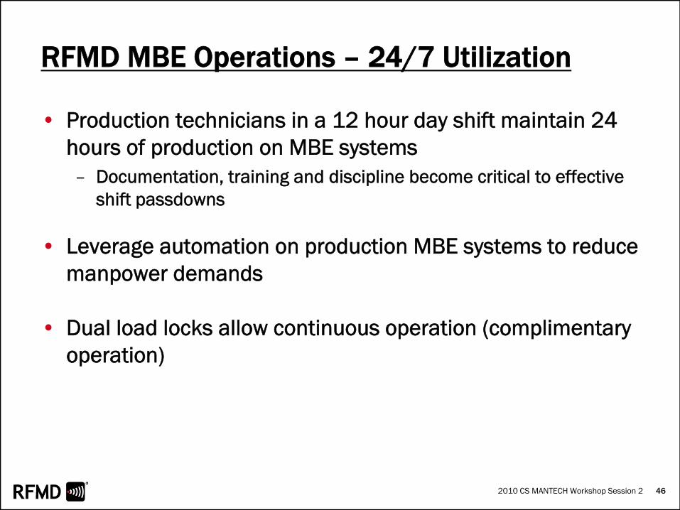
RFMD MBE Operations – 24/7 Utilization
• Production technicians in a 12 hour day shift maintain 24 hours of production on MBE systems– Documentation, training and discipline become critical to effective
shift passdowns
• Leverage automation on production MBE systems to reduce manpower demands
• Dual load locks allow continuous operation (complimentary operation)
2010 CS MANTECH Workshop Session 2 47
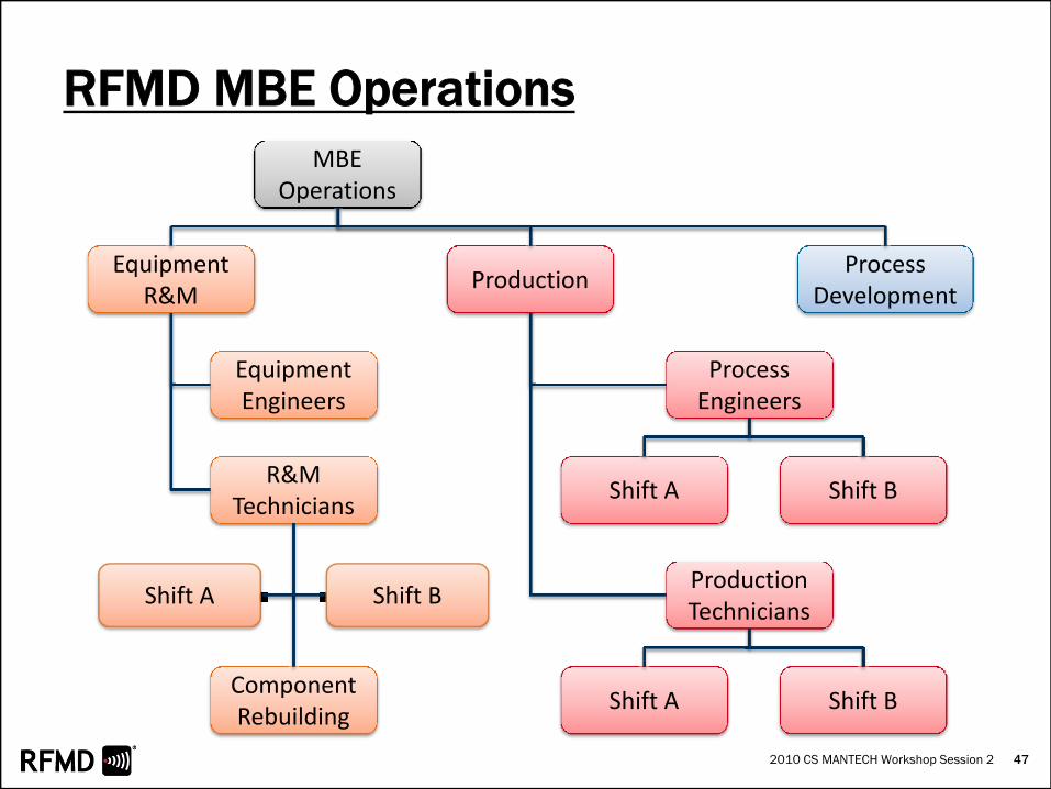
RFMD MBE OperationsMBE
Operations
Equipment R&M
Production
Equipment Engineers
R&M Technicians
Shift BShift A
Component Rebuilding
Process Engineers
Shift A Shift B
Process Development
Production Technicians
Shift A Shift B

2010 CS MANTECH Workshop Session 2 48
RFMD MBE Operations – System Management
Original Source Load Quantities
Known Consumption Rate per Epiwafer Run
Number of Runs Since Last Reload
2010 CS MANTECH Workshop Session 2 49
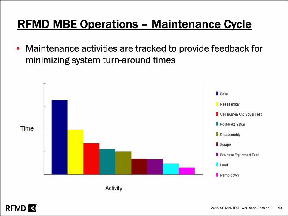
RFMD MBE Operations – Maintenance Cycle
• Maintenance activities are tracked to provide feedback for minimizing system turn-around times
2010 CS MANTECH Workshop Session 2 50
RFMD MBE Operations – Epi Characterization
• Epiwafer characterization data is monitored using online process control charts
• Daily check of SPC data provides feedback to alert Production technicians and engineers of any need for process adjustments
• Appropriate process adjustments are calculated with standardized tools− Input characterization data from recent runs− Input MBE process parameters from same runs− Outputs include setpoint correction

2010 CS MANTECH Workshop Session 2 51
RFMD MBE Operations – HBT “Quick Turn”
• Periodic sampling from every MBE tool growing HBT’s
• Essential for determining if device parameters are on target
• Additional information on doping levels of individual layers can eliminate the need for dedicated calibration runs− Base sheet resistance− Emitter sheet resistance− BVebo
• Process adjustments calculated with standardized tools
2010 CS MANTECH Workshop Session 2 52
RFMD MBE Operations – Fab Data• MBE process engineers monitor online trend charts
− Contact resistance− Doping levels and breakdown voltages− Current gain (HBT)− Turn-on voltage (HBT or pHEMT)
• Sampling of recent production epiwafers keeps in-process test data current (Modified FIFO)
• MBE process engineers held accountable for MBE related wafer fabyield loss− Wafer fab corrective action reports automatically assigned− MBE engineer may scrap additional wafers from epiwafer inventory− Create a culture in which MBE personnel realize wafer fab scrap is more
costly to business than epiwafer scrap

2010 CS MANTECH Workshop Session 2 53
RFMD MBE Operations – Continuous Improvement
• Ongoing efforts to improve yield and reduce variation− MBE epiwafer yield− Wafer fab line yield− Final product test yield
• Pareto analysis of scrap causes during monthly and quarterly reviews. (MBE yield and fab yield)
• Common databases provides traceability from GaAssubstrates through MBE and fab processing− Invaluable in determining correlations between MBE process
parameters, epiwafer characterization and device performance− Identify sources of variation that can be reduced to achieve specific
goals in product performance or yield

2010 CS MANTECH Workshop Session 2 54
Acknowledgements
• Thanks to the following people and companies for their assistance in producing this presentation:
– Phil Grunes, Sumitomo Electric Semiconductor Materials, Inc.
– Kevin Stevens, Charles Lutz and Eric Rehder,Kopin Corporation
– Molly Doran and Nate Groneberg, Veeco Instruments
– Tom Rogers, RFMD
Top Related