Zero Overvoltage Switching “ZOS” - iisb.fraunhofer.de · Version Whitepaper, Version...
5
FRAUNHOFER-INSTITUT FÜR INTEGRIERTE SYSTEME UND BAUELEMENTETECHNOLOGIE IISB Address Fraunhofer IISB Institut für Integrierte Systeme und Bauelementetechnologie Schottkystraße 10, 91058 Erlangen, Germany www.iisb.fraunhofer.de Departement Vehicle electronics Dr. Bernd Eckardt eMail: [email protected] | Tel: +49-9131-761-139 Version Whitepaper, Version 15.01.2018, published 16.01.2018 Author Stefan Matlok eMail: [email protected] | Tel: +49-9131-761-176 Zero Overvoltage Switching “ZOS” Breaking the rules of parasitic inductance
Transcript of Zero Overvoltage Switching “ZOS” - iisb.fraunhofer.de · Version Whitepaper, Version...

F R A U N H O F E R - I N S T I T U T F Ü R I N T E G R I E R T E S Y S T E M E U N D B A U E L E M E N T E T E C H N O L O G I E I I S B
Address Fraunhofer IISB Institut für Integrierte Systeme und Bauelementetechnologie Schottkystraße 10, 91058 Erlangen, Germany www.iisb.fraunhofer.de
Departement Vehicle electronics Dr. Bernd Eckardt eMail: [email protected] | Tel: +49-9131-761-139
Version Whitepaper, Version 15.01.2018, published 16.01.2018
Author Stefan Matlok eMail: [email protected] | Tel: +49-9131-761-176
Zero Overvoltage Switching “ZOS” Breaking the rules of parasitic inductance
Vehicle Power Electronics | Internal Research | Zero Overvoltage Switching Seite 1
1 Abstract Turning off an electrical path is causing trouble by parasitic inductance since beginning of power elec-tronics. Ages are spent to avoid oscillations and voltage overshoot while compromising on switching speed. Not only since new Wide Band Gap devices are available, a demand for new power modules and packages emerged and innovative low-inductance or resonant concepts have been introduced successfully. In contrast, the ZOS method offers a solution to unleash unlimited switching speed in real-world applications without overvoltage on the semiconductors. Moreover, in best case, it is even avoiding any subsequent parasitic oscillation. The idea is to use the intrinsic parasitic inductances and parasitic capacities to build up a resonant circuit. The turn off event excites the resonant circuit and the free-wheeling diode stops it automatically after half a period, e.g. after a view nanoseconds. These resonant parasitic elements are thereby utilized to switch off a fixed current in a lossless, overvoltage-, and EMI compliant way. By designing the circuit and parasitics properly, there is no extra component necessary and even relaxed industrial style semiconductor housings and low-budget capacitors can build up the circuit, as parasitic inductance is now functional part of the topology.
2 Explaining the ZOS Converter Circuit and Control Strategy The technology focuses on the switching-off transient, which is causing problems in typical hard-switched topologies. To simplify the problem, only a classic boost converter, as seen in Fehler! Ver-weisquelle konnte nicht gefunden werden., is described to explain the ZOS approach.
2.1 Classic Turn-Off Tbot is turned on for a specific time to increase the phase current IPh. During turn-off event, Tbot faces a so called voltage overshoot, which is necessary to force IPh through the parasitic inductance Lpar. In state-of-the art technology, Lpar should be as low as possible and switching speed of Tbot needs to be limited to keep the max. voltage overshoot below all SOA limits. That is also true on a more relaxed situation where Tbot is considered to have a parasitic or additional discrete capacitance Cpar in parallel.
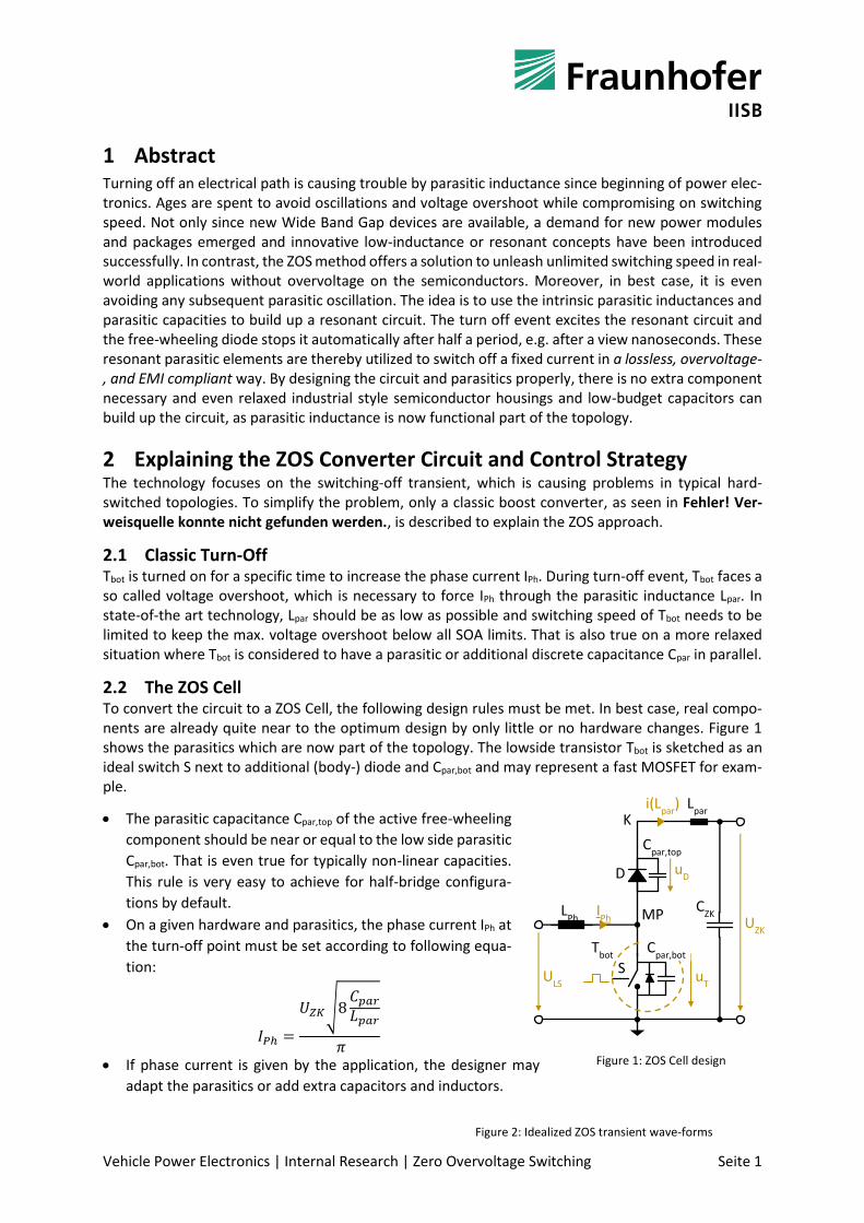
2.2 The ZOS Cell To convert the circuit to a ZOS Cell, the following design rules must be met. In best case, real compo-nents are already quite near to the optimum design by only little or no hardware changes. Figure 1 shows the parasitics which are now part of the topology. The lowside transistor Tbot is sketched as an ideal switch S next to additional (body-) diode and Cpar,bot and may represent a fast MOSFET for exam-ple.
The parasitic capacitance Cpar,top of the active free-wheeling
component should be near or equal to the low side parasitic
Cpar,bot. That is even true for typically non-linear capacities.
This rule is very easy to achieve for half-bridge configura-
tions by default.
On a given hardware and parasitics, the phase current IPh at
the turn-off point must be set according to following equa-
tion:
𝐼𝑃ℎ =
𝑈𝑍𝐾√8𝐶𝑝𝑎𝑟𝐿𝑝𝑎𝑟
𝜋
If phase current is given by the application, the designer may
adapt the parasitics or add extra capacitors and inductors.
S u
T
D
Lpar
CZK
LPh
MP IPh
ULS
UZK
K
uD
i(Lpar
)
Cpar,top
Cpar,bot
Tbot
Figure 1: ZOS Cell design
Figure 2: Idealized ZOS transient wave-forms

Vehicle Power Electronics | Internal Research | Zero Overvoltage Switching Seite 2
The chips and/or the gate driver must be de-
signed to turn off as fast and snappy as possi-
ble. That can be achieved e.g, by switching a
25 mΩ SiC MOSFET with a gate resistor RG of
less than 1 Ω. Less speed will eliminate the
ZOS effect.
Following these ZOS Cell rules, the ZOS effect oc-curs as follows:
Step 1: The channel S inside the transistor is shut off as fast as possible during t1, which may also take several ns in physical devices.
Step 2: Output capacitance is charged by the phase current IPh and thereby MP is rising. The parasitic top side capacity Cpar,top shifts the level of its cathode K over the DC link voltage UZK with-out any overvoltage on Tbot. Thereby i(Lpar) rises and oscillation begins.
Step 3: The oscillation ends immediately after half a period at t3 - exactly where the current i(Lpar) is at its maximum. In an ideal setup, the maximum equals IPh while uD is zero at this point. Furthermore, the oscillator is stopped by the freewheeling diode, which simply shortens Cpar,top.
2.3 Simulation Experiment One interesting ZOS showcase is a simulation experiment on varying the gate resistance Rgate. Following classic theory, overvoltage can be reduced by increasing the gate resistor. Following the rules of ZOS Cell design, it is shown how overvoltage can be decreased against all expectations by lowering the gate resistance (and raising switching speed). By that approach, the losses can be cut down to about 2 % of the nominal datasheet losses (in this simulation example) by applying an external Rgate of about 1 Ω (additional to the internal chip resistance) instead of 20 Ω recommended. The simulation turns off the optimum ZOS current of 84 A using the Cree SPICE Models, which are a good choice for transient sim-ulations.
Figure 3: ZOS Simulation of a SiC half bridge
0 V
200 V
400 V
600 V
800 V
1000 V
1200 V
0 ns 100 ns 200 ns 300 ns 400 ns 500 ns 600 ns 700 ns 800 ns
1 mΩ4.4 µJ
1 Ω18 µJ
2 Ω37 µJ
5 Ω162 µJ
10 Ω472 µJ 20 Ω
1115 µJ Identical to datasheet of CCS050M12CM2
50 Ω3068 µJ
Lowside Transistor Voltage u(Tbot) of Cree C2M0025120D Half Bridge Configuration
RgateEoff
ZOS Region
ClassicRegion
0 A
15 A
30 A
45 A
60 A
0 V
200 V
400 V
600 V
800 V
1000 V
1200 V
1400 V
0 ns 2 ns 4 ns 6 ns 8 ns 10 ns
i(S)i(Lpar)
u(K)
u(Tbot)
t1 t2 t3

Vehicle Power Electronics | Internal Research | Zero Overvoltage Switching Seite 3
Figure 4: Circuit of ZOS Half bridge simulation
2.4 Measurement Experiment Claiming overvoltage may disappear by increasing switching speed, adding parasitic inductance and ramp up the current is a very tough job resulting in disbelieve and shaking heads. That’s why a proof of concept test setup was build.
The setup available has a drawback as 4,3 Ω gate resistors per chip (optimum would be below 1 Ω) are used inside the power module. To compensate this issue as far as possible, -10 V negative gate voltage (instead of -5 V) was applied to switch off faster.
A Half bridge SiC module with 4x C2M0025120D per switch and 4x 10 A SiC diodes
Figure 5: ZOS test setup SiC power module with DC-Link PCB and film ca-pacitors
B Increased DC-Link inductance by adding about ~50 nH (2x100nH in parallel)
C Test voltage 400 V DC UZK D Test phase inductor connected
between MP and high side DC link
E uT measured by both Kelvin con-tacts SB and ST similar to Figure 4.
To proof that the ZOS effect exists, the current IPh was alternated by changing to on-time and thereby ramp up different current values. Figure 6 shows a turn off current of about 50 A. Figure 7 turns off at an even larger current of about 68 A but hitting ZOS operation point. The experiment can be done at different voltages, currents and parasitic inductances, all showing optimal ZOS point as long as the module is switched as fast as possible.
V2
25
V=
if(V
(d)>
0.5
,20,-
5)
B2
Tj
Tc
C2M0025120D
U2
L2
Lpar
PU
LS
E(0
I_
pu
lse
0.1
u 0
.1u
)
I1
PU
LS
E(1
0 1
u 1
n 1
n 1
u)
V1
PU
LS
E(0
80
0 0
0.1
u)
V6
R4
Rgate
B4
I=if((time<t_pulse),0,I(RM1)*V(MP))
C2
1µ
Tj
Tc
C2M
0025120
D
U5
V=
V(M
P,S
B)
B5
B6
I=if((time<t_pulse),0,V(U_cap_Bot)*-I(B5))
C4
1µ
D1
CP
W41
200S
020B
Tj
Tc
C2M0025120D
U1R1
Rgate
D2
CP
W41
200S
020B
R2
1m
RM1
1m
T
GB
SB
d
T
E_schein_Bot
T
E_cap_Bop
U_cap_Bot
T
GT
GB
ST
SB
MP
HS_HalfBridgeS
TG
T
.include C2M0025120D - Die.lib
.tran 0 2u 0.9u 1000p startup
.meas TRAN Peak_HS MAX V(MP)-800
.include Cree Power CPW4 Bare Die SPICE Model Library.lib
.step param Rgate list 1m 1 2 5 10 20 50
.param t_pulse 1u
.param I_pulse 84
.param Lpar = 20n.meas TRAN Energy_uJ MAX V(E_schein_Bot,E_cap_Bop)
A
B B C
D
E

Vehicle Power Electronics | Internal Research | Zero Overvoltage Switching Seite 4
Figure 6: Turning off a non optimal Current
Figure 7: Turning off the ZOS optimized current
Channel 4 (green) shows the inductor current. Channel 2 (light blue) shows the voltage across the low-side transistor. Channel 1 (dark blue) is a trigger reference of the pulse generator input signal.
2.5 Further Key Aspects The key point of these rules is the unlimited switching speed that allows cutting losses down to zero. Combined with classic Zero Voltage Switching (ZVS) during turn-on, it is possible to build up a real-world converter without significant switching losses at all.
Most applications need a power regulation. Several techniques allow set up average current while keeping optimum IPh at turn-off point:
Varying IPh around optimal ZOS point is still sufficient, e.g. by ±5%
Switch off phases on multi-phase designs would allow NPh-step regulation
Under recommended BCM operation, frequency can be reduced by Valley Skipping, enabling
current reduction approximately by factor 2
Finally, controlling power down to zero is always possible by classic burst-mode operation.
2.6 Applications The ZOV technology can be used in every converter technology being able to control the current during the turn-off operation point. That is possible for nearly any classic isolated and non-isolated Buck-, Boost-, Forward-, Phase-shift, Flyback- and other DC-DC converters from zero watts Point-of-Load con-verters to megawatt switching cells. Even load regulation is possible, implementation is more easy for constant-power applications like LED illumination or on-board chargers.
A very interesting application is also a Flyback converter. In this case, the converter can use the stray inductance of the transformer and the secondary side diode to model the ZOS effect. As there is no overvoltage and oscillation, no RC, RCD, or active snubber is necessary.
About the applicant: Dipl.- Ing. Stefan Matlok (28. December 1985) studied Mechatronics at the Friedrich Alexander University Erlangen majoring in power electronics. Since 2011, he specialized on switching circuit designs and develops FPGA and μC control boards for high power traction converters. As head of the DC/DC converter group at the Fraunhofer IISB, he works on new prospects improv-
ing functional features, power density, EMI, efficiency, and digital control techniques.
Since 2001: Web Applications, Embed-ded Software- and Power Electronic Hardware de-velopment
2005 – 2011: Mechatronics Diploma at the FAU Erlangen
2010: Internship Talent at the Semikron B4
2011-2013: Power Electronics at the Fraunhofer IISB
Since 2014: Head of Group DC/DC Converters at the Fraun-hofer IISB