Z80 CPU User’s Manual - Budapest University of...
25
Z80 CPU User’s Manual UM008003-1202 Overview 2 Figure 1. Z80 CPU Block Diagram 13 CPU and System Control Signals Inst. Register Data Bus Control Internal Data Bus CPU Registers ALU CPU Control Address Control 16-Bit Address Bus +5V GND CLK I n
Transcript of Z80 CPU User’s Manual - Budapest University of...

Z80 CPUUser’s Manual
UM008003-1202 Overview
2
Figure 1. Z80 CPU Block Diagram
13CPU andSystemControlSignals
Inst.Register
Data BusControl
Internal Data Bus
CPURegisters
ALU
CPUControl
AddressControl
16-BitAddress Bus+5V GND CLK
In

Z80 CPUUser’s Manual
UM008003-1202 Overview
7
Figure 3. Z80 I/O Pin Configuration
SystemControl
CPUControl
CPUBusControl
Z80 CPU
AddressBus
DataBus
A0A1A2A3A4A5A6A7A8A9A10A11A12A13A14A15
D0D1
D3D4D5D6D7
D2
3031323334353637383940
141512
879
1013
12345
M1
MREQIORQRDWR
RFSH
HALT
INTNMI
RESET
BUSRQBUSACK
CLK+5VGND
WAIT
27
19202122
26
18
24
1617
28
2523
61129

Z80 CPUUser’s Manual
UM008003-1202 Overview
12
Figure 4. Basic CPU Timing Example
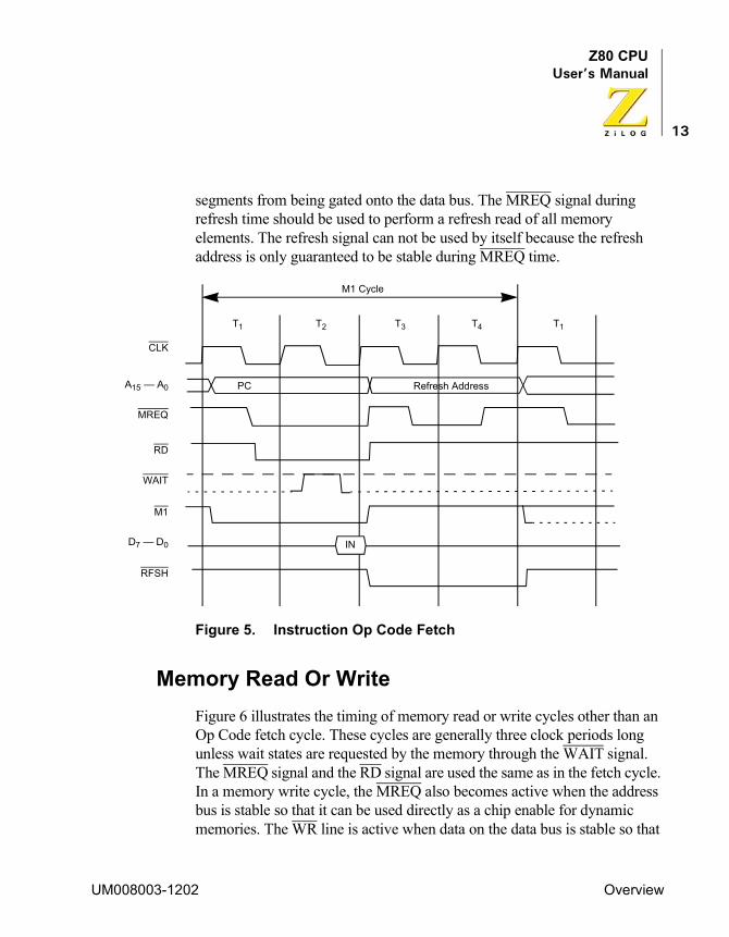
Instruction FetchFigure 5 depicts the timing during an M1 (opcode fetch) cycle. The PC is placed on the address bus at the beginning of the M1 cycle. One half clock cycle later the MREQ signal goes active. At this time the address to the memory has had time to stabilize so that the falling edge of MREQ can be used directly as a chip enable clock to dynamic memories. The RD line also goes active to indicate that the memory read data should be enabled onto the CPU data bus. The CPU samples the data from the memory on the data bus with the rising edge of the clock of state T3 and this same edge is used by the CPU to turn off the RD and MREQ signals. Thus, the data has already been sampled by the CPU before the RD signal becomes inactive. Clock state T3 and T4 of a fetch cycle are used to refresh dynamic memories. The CPU uses this time to decode and execute the fetched instruction so that no other operation could be performed at this time.
During T3 and T4, the lower seven bits of the address bus contain a memory refresh address and the RFSH signal becomes active tindicating that a refresh read of all dynamic memories must be accomplished. An RD signal is not generated during refresh time to prevent data from different memory
CLK
T Cycle
Machine CycleM1
(Opcode Fetch)
Instruction Cycle
M2(Memory Read)
M3(Memory Write)
T1 T1 T1T2 T2 T2T3 T3 T3
Z80 CPUUser’s Manual
UM008003-1202 Overview
13
segments from being gated onto the data bus. The MREQ signal during refresh time should be used to perform a refresh read of all memory elements. The refresh signal can not be used by itself because the refresh address is only guaranteed to be stable during MREQ time.
Figure 5. Instruction Op Code Fetch
Memory Read Or WriteFigure 6 illustrates the timing of memory read or write cycles other than an Op Code fetch cycle. These cycles are generally three clock periods long unless wait states are requested by the memory through the WAIT signal. The MREQ signal and the RD signal are used the same as in the fetch cycle. In a memory write cycle, the MREQ also becomes active when the address bus is stable so that it can be used directly as a chip enable for dynamic memories. The WR line is active when data on the data bus is stable so that
PC Refresh Address
T1 T2 T3 T4 T1
M1 Cycle
CLK
D7 — D0
A15 — A0
MREQ
RD
WAIT
M1
RFSH
IN

Z80 CPUUser’s Manual
UM008003-1202 Overview
14
it can be used directly as a R/W pulse to virtually any type of semiconductor memory. Furthermore, the WR signal goes inactive one-half T state before the address and data bus contents are changed so that the overlap requirements for almost any type of semiconductor memory type is met.
Figure 6. Memory Read or Write Cycle
Input or Output CyclesFigure 7 illustrates an I/O read or I/O write operation. During I/O operations a single wait state is automatically inserted. The reason is that during I/O operations, the time from when the IORQ signal goes active until the CPU must sample the WAIT line is very short. Without this extra state, sufficient time does not exist for an I/O port to decode its address and activate the WAIT line if a wait is required. Also, without this wait state, it is difficult to design MOS I/O devices that can operate at full CPU speed. During this wait state time, the WAIT request signal is sampled.
During a read I/O operation, the RD line is used to enable the addressed port onto the data bus just as in the case of a memory read. For I/O write operations, the WR line is used as a clock to the I/O port.
CLK
D7 — D0
A15 — A0
MREQ
RD
WAIT
WR
Memory AddressMemory Address
T2 T3 T1 T2 T3
In
Memory Read Cycle Memory Write Cycle
Data Out

Z80 CPUUser’s Manual
UM008003-1202 Overview
15
Figure 7. Input or Output Cycles
Bus Request/Acknowledge Cycle Figure 8 illustrates the timing for a Bus Request/Acknowledge cycle. The BUSREQ signal is sampled by the CPU with the rising edge of the last clock period of any machine cycle. If the BUSREQ signal is active, the CPU sets its address, data, and tristate control signals to the high-impedance state with the rising edge of the next clock pulse. At that time, any external device can control the buses to transfer data between memory and I/O devices. (This operation is generally known as Direct Memory Access [DMA] using cycle stealing.) The maximum time for the CPU to respond to a bus request is the length of a machine cycle and the external controller can maintain control of the bus for as many clock cycles as is required. If very long DMA cycles are used, and dynamic memories are used, the external controller also performs the refresh function. This situation only occurs if very large blocks of data
Out
T1 T1T2 T3TW*
WriteCycle
ReadCycle
Port Address
CLK
D7 — D0
A15 — A0
IORQ
RD
WAIT
WR
D7 — D0
*Automatically inserted WAIT state
In

Z80 CPUUser’s Manual
UM008003-1202 Overview
16
are transferred under DMA control. During a bus request cycle, the CPU cannot be interrupted by either an NMI or an INT signal.
Figure 8. Bus Request/Acknowledge Cycle
Interrupt Request/Acknowledge CycleFigure 9 illustrates the timing associated with an interrupt cycle. The CPU samples the interrupt signal (INT) with the rising edge of the last clock at the end of any instruction. The signal is not accepted if the internal CPU software controlled interrupt enable flip-flop is not set or if the BUSREQ signal is active. When the signal is accepted, a special M1 cycle is generated. During this special M1 cycle, the IORQ signal becomes active (instead of the normal MREQ) to indicate that the interrupting device can place an 8-bit vector on the data bus. Two wait states are automatically added to this cycle. These states are added so that a ripple priority interrupt scheme can be easily implemented. The two wait states allow sufficient time for the ripple signals to stabilize and identify which I/O device must insert the response vector. Refer to Chapter 6 for details on how the interrupt response vector is utilized by the CPU.
Sample Sample
Floating
Last T State TX TX TX T1
Any M Cycle Bus Available Status
CLK
D7 — D0
A15 — A0
BUSREQ
MREQ, RD
BUSACK
WR. IORQ,RFSH

Z80 CPUUser’s Manual
UM008003-1202 Overview
17
Figure 9. Interrupt Request/Acknowledge Cycle
Non-Maskable Interrupt ResponseFigure 10 illustrates the request/acknowledge cycle for the non-maskable interrupt. This signal is sampled at the same time as the interrupt line, but this line takes priority over the normal interrupt and it can not be disabled under software control. Its usual function is to provide immediate response to important signals such as an impending power failure. The CPU response to a non-maskable interrupt is similar to a normal memory read operation. The only difference is that the content of the data bus is ignored while the processor automatically stores the PC in the external stack and jumps to location 0066H. The service routine for the non-maskable interrupt must begin at this location if this interrupt is used.
In
RefreshPC
M1Last M Cycle of Instruction
CLK
D7 — D0
A15 — A0
INT
MREQ
RD
WAIT
T1 T2 TW* T3TW*
M1
IORQ
Last T State

Z80 CPUUser’s Manual
UM008003-1202 Overview
18
Figure 10. Non-Maskable Interrupt Request Operation
HALT ExitWhenever a software HALT instruction is executed, the CPU executes NOPs until an interrupt is received (either a non-maskable or a maskable interrupt while the interrupt flip-flop is enabled). The two interrupt lines are sampled with the rising clock edge during each T4 state as depicted in Figure 11. If a non-maskable interrupt has been received or a maskable interrupt has been received and the interrupt enable flip-flop is set, then the HALT state is exited on the next rising clock edge. The following cycle is an interrupt acknowledge cycle corresponding to the type of interrupt that was received. If both are received at this time, then the non-maskable one is acknowledged since it has highest priority. The purpose of executing NOP instructions while in the HALT state is to keep the memory refresh signals active. Each cycle in the HALT state is a normal M1 (fetch) cycle except that the data received from the memory is ignored and a NOP instruction is forced internally to the CPU. The HALT acknowledge signal is active during this time indicating that the processor is in the HALT state.
CLK
A15 — A0
NMI
MREQ
RD
RFSH
T1 T2 T3
M1
Refresh
M1Last M Cycle
Last T State
PC
T1T4

Z80 CPUUser’s Manual
UM008003-1202 Overview
3
Figure 2. Z80 CPU Register Configuration
GeneralPurposeRegisters
Accumulator
H '
SpecialPurposeRegisters
Index Register
Index RegisterStack PointerProgram Counter
Interrupt VectorI
H L L 'D E D ' E 'B C B ' B 'A F A ' F '
Flags Accumulator Flags
Alternate Register SetMain Register Set
Memory RefreshRIXIYSPPC

Z80 CPUUser’s Manual
UM008003-1202 Z80 Instruction Set
76
Z80 Status Indicator FlagsThe flag registers (F and F') supply information to the user about the status of the Z80 at any given time. The bit positions for each flag is listed below:
Each of the two flag registers contains 6 bits of status information that are set or cleared by CPU operations. (Bits 3 and 5 are not used.) Four of these bits (C, P/V, Z, and S) may be tested for use with conditional JUMP, CALL, or RETURN instructions. Two flags may not be tested (H, N) and are used for BCD arithmetic.
Carry FlagThe Carry Flag (C) is set or cleared depending on the operation performed. For ADD instructions that generate a Carry, and SUB instructions that generate a Borrow, the Carry Flag sets. The Carry Flag is reset by an ADD instruction that does not generate a Carry, and by a SUB instruction that does not generate a Borrow. This saved Carry facilitates software routines
7 6 5 4 3 2 1 0S Z X N X P/V N C
Symbol Field NameC Carry FlagN Add/SubtractP/V Parity/Overflow FlagH Half Carry FlagZ Zero FlagS Sign FlagX Not Used

Z80 CPUUser’s Manual
UM008003-1202 Z80 CPU Instruction Description
51
Table 2. 8-Bit Load Group LD t our
Source
Implied Register Reg Indirect 11indexed Ext Addr. Imme.
Destination I R A B C D E F L (HL) (BC) (DE) (IX+d) (lY+d) Inn) n
Register A ED57
ED5F
7F 78 79 7A 7B 7C 7D 7E 0A 1A FD7Ed
DD7Ed
FD3Ann
FD2En
B 47 40 41 42 43 44 45 46 DD46d
FD46d
DDD5n
C 4F 48 49 4A 4B 4C 4D 4E DD4Ed
FD4Ed
DDDEn
D 57 50 51 52 53 54 55 56 DD56d
FD56d
DD1Bn
E 5F 58 59 5A 5B 5C 5D 5E DD5Ed
FD5Ed
DD1En
H 67 60 61 62 63 64 65 66 DD66d
FD66d
DD2Bn
L 6F 68 69 6A 6B 6C 6D 6E DD6Ed
FD6Ed
DD36n
RegIndirect
(HL) 77 70 71 72 73 74 75 DD78D
(BC) 02
(DE) 12
INDEXED (IX+d) DD77d
DD70d
DD71d
DD72d
DD73d
DD74d
DD75d
DD36dn
(IY+d) FD77d
FD70d
FD71d
FD72d
FD73d
FD74d
FD75d
FD36dn
EXT,ADDR
(nn) 32nn
.
IMPLIED I ED47
R ED4F

Z80 CPUUser’s Manual
UM008003-1202 Z80 CPU Instruction Description
55
Table 3. 16-Bit Load Group LD t our , PUSH op and POP op
Source
Register Imm. Ext. Ext. Addr. Reg. Indir.
Register AF BC DE HL SP IX IY nn (nn) (SP)
AF P1
BC 01nn
ED4Bnn
C1
DE 11nn
ED5Bnn
D1
HL 21nn
2Ann
E1
SP F9 DDF9
FDF9
31nn
ED7Bnn
IX DD21nn
DD2Ann
DDE1
IY FD21nn
FD2Ann
FDE1
EXTADDR.
(nn) ED43nn
ED53nn
22nn
ED73nn
DD22nn
FD22nn
PUSH Instructions �
REG.IND.
(SP) F6 C6 D6 E6 DDE6
FDE6
NOTE: The Push & Pop instruction adjust the SP after every execution. ¦POPInstructions

Z80 CPUUser’s Manual
UM008003-1202 Z80 CPU Instruction Description
58
Arithmetic and LogicalTable 7 lists all the 8-bit arithmetic operations that can be performed with the accumulator, also listed are the increment (INC) and decrement (DEC)
Table 5. Block Transfer Group
Destination SourceReg. Indir. (DE) Reg. Indir.
(HL)
(ED)A0
LDI - Load (DE) ��(HL)Inc HL and DE, Dec BC
(ED)B0
LDIR, - Load (DE) �(HL)Inc HL and DE, Dec BC, Repeat until BC = 0
(ED)A8
LDD - Load (DE) � (HL)Inc HL and DE, Dec BC
(ED)B8
LDDR - Load (DE) � (HL)Dec HL and DE, Dec BC, Repeat until BC = 0
Note: Reg HL points to sourceReg DE points to destinationReg BC is byte counter
Table 6. Block Search Group
Search LocationReg. Indir.
(HL)
(ED)A1
CPIInc HL, Dec BC
(ED)B1
CPRI. Inc HL, Dec BCRepeat until) BC = 0 or find match
(ED)A9
WD Dec HL and BC
(ED)B9
CPDR Dec HL and BCRepeat until BC = 0 or find match
Note: HL points to location in memory to be compared with accumulator contentsBC Is byte counter

Z80 CPUUser’s Manual
UM008003-1202 Z80 CPU Instruction Description
60
Five general-purpose arithmetic instructions operate on the accumulator or carry flag. These five are listed in Table 8. The decimal adjust instruction can adjust for subtraction as well as addition, making BCD arithmetic operations simple. Note that to allow for this operation the flag N is used. This flag is set if the last arithmetic operation was a subtract. The negate accumulator (NEG) instruction forms the two’s complement of the number in the accumulator. Finally, notice that a reset carry instruction is not included in the Z80 because this operation can be easily achieved through other instructions such as a logical AND of the accumulator with itself.
Table 9 lists all the 16-bit arithmetic operations between 16-bit registers. There are five groups of instructions including add with carry and subtract with carry. ADC and SBC affect all the flags. These two groups simplify address calculation operations or other 16-bit arithmetic operations.
Table 7. 8-Bit Arithmetic and Logic
Source
Register Addressing Reg Indir. Indexed Immed.
A B C D E F L (HL) (IX+d) (lY+d) n
ADD 87 80 81 82 83 84 85 88 DD86d
FD86d
C6n
ADD W CARRY ADC
8F 88 89 8A 8B 8C 8D 8E DD8Ed
FD8Ed
CEn
SUBTRACTSUB
97 90 91 92 93 94 95 96 DD96d
FD96d
D6n
SUB w CARRSBC
9F 98 99 9A 9B 9C 9D 9E DD9Ed
FD9Ed
DEn
AND A7 A0 A1 A2 A3 A4 A5 A6 DDA6d
FDA6d
E6n
XOR AF A8 A9 AA AB AC AD AE DDAEd
FDAEd
EEn

Z80 CPUUser’s Manual
UM008003-1202 Z80 CPU Instruction Description
61
OR B7 B0 B1 B2 B3 B4 B5 B6 DDB6d
FDB6d
F6n
COMPARECP
BF B8 B9 BA BB BC BD BE DDBEd
FDBEd
FEn
INCREMENTINC
3C 04 0C 14 1C 24 2C 34 DD34d
FD34d
DECREMENTDEC
3D 05 0D 15 1D 25 2D 35 DD35d
FD35d
Table 8. General-Purpose AF Operation
Decimal Adjust Acc, DAA 27
Complement Acc, CPL 2F
Negate Acc, NEG(2’s complement
ED44
Complement Carry Flag, CCF 3F
Set Carry Flag, SCF 37
Table 9. 16-Bit Arithmetic
SourceBC DE HL SP IX IY
Table 7. 8-Bit Arithmetic and Logic
Source
Register Addressing Reg Indir. Indexed Immed.

Z80 CPUUser’s Manual
UM008003-1202 Z80 CPU Instruction Description
62
Rotate and ShiftA major feature of the Z80 is to rotate or shift data in the accumulator, any general-purpose register, or any memory location. All the rotate and shift Op Codes are depicted in Figure 10. Also included in the Z80 are arithmetic and logical shift operations. These operations are useful in a wide range of applications including integer multiplication and division. Two BCD digit rotate instructions (RRD and RLD) allow a digit in the accumulator to be rotated with the two digits in a memory location pointed to by register pair HL (See Figure 10). These instructions allow for efficient BCD arithmetic.
Destination HL 09 19 29 39
ADD IX DD09
DD19
DD39
DD29
IY FD09
FD19
FD39
FD29
ADD with carry and set flags ADC HL ED4A
ED5A
ED6A
ED7A
SUB with carry and set flags SBC HL ED42
ED52
ED62
ED72
Increment INC 03 13 23 33 DD23
FD23
Decrement DEC DB 1B 2B 3B DD2B
FD2B
Table 9. 16-Bit Arithmetic
Source

Z80 CPUUser’s Manual
UM008003-1202 Z80 CPU Instruction Description
63
Bit ManipulationThe ability to set, reset, and test individual bits in a register or memory location is needed in almost every program. These bits may be flags in a general-purpose software routine, indications of external control
Table 10. Rotates and Shifts
Source
Type ofRotateShift
A B C D E F L (HL) (IX+d) (lY+d) A
RCL CB07
CB00
CB01
CB02
CB03
CB04
CB06
CB0E
DDCBd06
FDCBd06
RLCA D7
RRC CB0F
CB08
CB09
CB0A
CB06
CB0C
CB0D
CB0E
DDCBd0E
FDCBd0E
RRCA 0F
RL CB17
CB10
CB11
CB12
CB13
CB14
CB15
CB16
DDCBd16
FDCBd16
RLA 17
RR CB1F
CB18
CB19
CB1A
CB1B
CB1C
CB1D
CB1E
DDCBd1E
FDCBd1E
RRA 1F
SLA CB27
CB20
CB21
CB22
CB23
CB24
CB25
CB26
DDCBd26
FDCBd26
SRA CB2F
CB28
CB29
CB2A
CB2B
CB2C
CB2D
CB2E
DDCBd2E
FDCBd2E
SRL CB3F
CB38
CB39
CB3A
CB3B
CB3C
CB3D
CB3E
DDCBd3E
FDCBd3E
ED6F
ED67
CY
CY
0
ACC
ACC
RotateLeft Circular
RotateRight Circular
RotateLeft
RotateRight
ShiftLeft Arithmetic
ShiftRight Arithmetic
ShiftRight Logical
(HL)
(HL)
b7 b0
b7-b4 b3-b0b3-b0
RotateDigitRight
RotateDigitLeft

Z80 CPUUser’s Manual
UM008003-1202 Z80 CPU Instruction Description
66
TestBit
0 C8 C8 C8 C8 C8 C8 C8 C8 C8 C8
47 40 41 42 43 44 45 46 d d
46 46
DD FD
1 C8 C8 C8 C8 C8 C8 C8 C8 C8 C8
4F 48 49 4A 48 4C 4D 4E d d
4E 4E
DD FD
2 C8 C8 C8 C8 C8 C8 C8 C8 C8 C8
57 50 51 52 53 54 55 56 d d
56 56
DD FD
3 C8 C8 C8 C8 C8 C8 C8 C8 C8 C8
5F 58 59 5A 5B 5C 5D 5E d d
46 46
DD FD
4 C8 C8 C8 C8 C8 C8 C8 C8 C8 C8
67 60 61 62 63 64 65 66 d d
66 66
DD FD
5 C8 C8 C8 C8 C8 C8 C8 C8 C8 C8
6F 68 69 6A 68 6C 6D 6E d d
6E 6E
DD FD
6 C8 C8 C8 C8 C8 C8 C8 C8 C8 C8
77 70 71 72 73 74 75 76 d d
76 76
DD DD
7 C8 C8 C8 C8 C8 C8 CS C8 C8 C8
7F 78 79 7A 78 7C 7D 7E d d
46 46
Table 11. Bit Manipulation Group (Continued)
Register Addressing Reg. Indir. Indexed

Z80 CPUUser’s Manual
UM008003-1202 Z80 CPU Instruction Description
67
RestBitRES
DD FD
0 C8 C8 C8 C8 C8 C8 C8 C8 C8 C8
87 80 81 82 83 84 85 86 d d
86 86
DD FD
1 C8 C8 C8 C8 C8 C8 C8 C8 C8 C8
8F 88 89 8A 88 8C 8D 8E d d
8E 8E
DD FD
2 C8 C8 CS C8 C8 C8 C8 C8 C8 C8
97 90 91 92 93 94 95 96 d d
96 96
DD FD
3 C8 C8 C8 C8 CS C8 C8 C8 C8 C8
9F 98 99 9A 98 90 90 9E d d
9E 9E
DD FD
4 C8 C8 C8 C8 C6 C8 C8 C8 C8 C8
A7 AO AI A2 A3 A4 A5 A6 d d
A6 A6
DD FD
5 C8 C8 C8 C8 08 C8 C8 C8 C8 C8
AF A8 A9 AA AB AC AD AE d d
AE AE
DD FD
6 C8 C8 C8 C8 C8 C8 C8 C8 C8 C8
B7 B0 B1 82 B3 B4 B5 B6 d d
B6 B6
DD DD
7 C8 C8 C8 C8 C8 C8 C8 C8 C8 C8
BF B8 89 8A B8 8C BD 9E d d
BE BE
Table 11. Bit Manipulation Group (Continued)
Register Addressing Reg. Indir. Indexed

Z80 CPUUser’s Manual
UM008003-1202 Z80 CPU Instruction Description
68
SetBitSET
DD FD
0 C8 C8 C8 C8 C8 C8 C8 C8 C8 C8
C7 C0 C1 C2 C3 C4 C5 C6 d d
C6 C6
DD FD
1 C8 C8 C8 C8 C8 C8 C8 C8 C8 C8
CF C8 C9 CA C8 CC CD CE d d
CE CE
DD FD
2 C8 C8 C8 C8 C8 C8 C8 C8 C8 C8
D7 DO D1 D2 D3 D4 DS D6 d d
D6 D6
DD FD
3 C8 C8 C8 C8 C8 C8 C8 C8 C8 C8
DF D8 09 DA DS DC DD DE d d
DE DE
DD FD
4 C8 C8 C8 C8 C8 C8 C8 C8 C8 C8
E7 E0 E1 E2 E3 E4 E5 E6 d d
E6 E6
DD FD
5 C8 C8 C8 C8 C8 C8 C8 C8 C8 C8
EF E8 E9 EA EB EC ED EE d d
EE EE
DD FD
6 C8 C8 C8 C8 C8 C8 C8 C8 C8 C8
F7 FO F1 F2 F3 F4 FS F6 d d
F6 F6
DD FD
7 C8 C8 C8 C8 C8 C8 C8 C8 C8 C8
FF F8 F9 FA FB FC FD FE d d
FE FE
Table 11. Bit Manipulation Group (Continued)
Register Addressing Reg. Indir. Indexed

Z80 CPUUser’s Manual
UM008003-1202 Z80 CPU Instruction Description
69
The instruction DJNZ is used to facilitate program loop control. This two byte, relative jump instruction decrements the B register and the jump occurs if the B register has not been decremented to zero. The relative displacement is expressed as a signed two’s complement number. A simple example of its use is:
Table 12. Jump, Call, and Return Group
Condition
Un-Cond.
Carry NonCarry
Zero NonZero
ParityEven
ParityOdd
SignNeg
SignPos
RegB�0
JUMP JP IMMED.EXT.
nn C3nn
D8nn
D2nn
CAnn
C2nn
EAnn
E2nn
FAnn
F2nn
JUMP JR RELATIVE PC+e 18e-2
38e-2
30e-2
28e-2
20e-2
JUMP JP RegisterINDIR.
(HL) EB
(IX) DDE9
(IY) FDE9
CALL IMMED.EXT.
nn CDnn
DCnn
D4nn
CCnn
C4nn
ECnn
E4nn
FCnn
F4nn
Decrement B, Jump If Non Zero DJNZ
RELATIVE PC+e 10e-2
Return RE REGISTERINDIR.
(SP)(SP+1)
C9 D8 D0 C8 C0 E8 E0 F8 F0
Return FromINT RETI
ED4D
Return FromNon MaskableINT RETN
ED45
Address Instruction CommentsN, N+1 LD B, 7 : set B register to count of 7
N+2 to N+9 (Perform a sequence of instructions) : loop to be performed 7 times
N+10,N+11 DJNZ -8 : to jump from N+12 to N+2
N + 12 (Next Instruction)

Z80 CPUUser’s Manual
UM008003-1202 Z80 CPU Instruction Description
70
Table 13 lists the eight Op Codes for the restart instruction. This instruction is a single byte call to any of the eight addresses listed. The simple mnemonic for these eight calls is also listed. This instruction is useful for frequently-used routines because memory consumption is minimized.
Input/OutputThe Z80 has an extensive set of input and output instructions as shown in Table 14 and Table 15. The addressing of the input or output device can be either absolute or register indirect, using the C register. In the register indirect addressing mode, data can be transferred between the I/O devices and any of the internal registers. In addition, eight block transfer instructions have been implemented. These instructions are similar to the memory block transfers except that they use register pair HL for a pointer to the memory source (output commands) or destination (input commands) while register B is used as a byte counter. Register C holds the address of the port for which the input or output command is required. Because register B is eight bits in length, the I/O block transfer command handles up to 256 bytes.
In the instructions IN A, and OUT n, A, the I/O device address n appears in the lower half of the address bus (A7-A0) while the accumulator content
Table 13. Restart Group
Op Code
CALL Address 0000H C7 RST 0
0008H CF RST 8
0010H D7 RST 16
0018H DF RST 24
0020H E7 RST 32
0028H EF RST 40
0030H F7 RST 48
0038H FF RST 56

Z80 CPUUser’s Manual
UM008003-1202 Z80 CPU Instruction Description
72
Table 14. Input Group
Immed.RegisterIndir.
(n) (c)
InputDestination
Input IN RegisterAddress
A DBn
ED7B
B ED40
C ED48
D ED50
E ED58
H ED60
L ED68
INI - input &inc HL, Dec B
RegisterIndir
(HL) EDA2
Block InputCommandsINIR - INP, Inc HL,
Dec B, repeat IF B�0EDB2
IND - input & IncDec HL, Dec B
EDAA
INDR - input, Dec HL,Dec B, repeat IF B�0
EDBA

Z80 CPUUser’s Manual
UM008003-1202 Z80 CPU Instruction Description
73
Table 15. Output group
SourceRegister Register Indir.A B C D E H L (HL)
OUT Immed. (n) D3n
RegInd.
(c) ED79
ED41
ED49
ED51
ED59
ED61
ED69
OUT - outputinc HL, dec B
EDA3
BlockOutputCommandOUT - output
dec B, repeat if B�0EDB3
OUT - outputdec HL and B
EDAB
OUTDR - output, dec HL and B, repeat IF B�0
EDBB
PortDestinationAddress
Table 16. Miscellaneous CPU ControlNOP 00HALT 76Disable INT (EI) F3Enable INT (EI) FBSet INT mode 0IM0
ED46
8080A mode
Set INT mode 1IM1
ED56
Call to location 0038H
Set INT mode 2IM2
ED5E
indirect call using register I and Bbits from INTER device as a pointer