BOND PRICE VOLATILITY. PRICE YIELD PRICE YIELD RELATIONSHIP CONVEX SHAPE.

33Yield and
Yield Management

Clearly line yield and defect density are twoof the most closely guarded secrets in thesemiconductor industry. Line yield refers tothe number of good wafers produced with-out being scrapped, and in general, measuresthe effectiveness of material handling,process control, and labor. Die yield refers tothe number of good dice that pass waferprobe testing from wafers that reach thatpart of the process. It is intended to preventbad dice from being assembled into pack-ages that are often extremely expensive andmeasures the effectiveness of process control,design margins, and particulate control.Figure 3-1 shows some typical numbers for afew product types normalized to twentymasking layers, similar feature and die sizes,and the Murphy defect density model.
Yield improvement is the most critical goalof all semiconductor operations as it reflectsthe amount of product that can be sold rela-tive to the amount that is started. Yield is alsothe single most important factor in overallwafer processing costs. That is, incrementalincreases in yield (1 or 2 percent) signifi-cantly reduce manufacturing cost per wafer,or cost per square centimeter of silicon. In thefab, yield is closely tied to equipment perfor-mance (process capability), operator train-ing, overall organizational effectiveness, andfab design and construction.
Continued device miniaturization in thesemiconductor industry and the trend tolarger and larger die sizes means that partic-ulate contamination has an ever increasingimpact on yields. Today, over 80 percent ofyield loss of VLSI chips manufactured involume can be attributed to random defects.The other main contributors to yield lossinclude design margin and process variation,followed by photolithography errors, andmaterial (wafer) defects (Figure 3-2). Thedramatic decline in the contribution ofpeople to particulate problems in the fab canbe attributed to better education and train-ing, adherence to clean room disciplines, andless direct contact by the people due to moreuse of automation.
INTEGRATED CIRCUIT ENGINEERING CORPORATION 3-1
3 Yield and Yield Management
Product MetricBest
ScoreAverage
ScoreWorstScore
Memory
CMOS Logic
MSI
Line Yield
Die Yield
Line Yield
Die Yield
Line Yield
Die Yield
98.8
93.6
97.2
78.6
91.2
56.7
93.0
77.4
89.8
71.1
77.9
49.5
87.1
52.8
77.8
48.6
65.9
43.1
* 2Q mask layers, ~1m feature size, 0.5sq. cmSource: UC Berkeley Study 22793
Figure 3-1. Typical Line Yield and Die Yields(Normalized*)

Yield and Yield Management
INTEGRATED CIRCUIT ENGINEERING CORPORATION3-2
Random defects can be traced back to thetools, the people, the processes, the processchemicals and gases, or the cleanroom itself.Over the years, cleanroom technology andthe purification of process materials has beenimproved so dramatically that the majority
of contamination in leading-edge fabs todayis due to the processes and tools (Figure 3-3).However, for many existing fabs, cleanroomcontamination remains a significant, yield-limiting factor.
CONTAMINATION
DESIGN MARGIN
PROCESS VARIATION
PHOTOLITHOGRAPHY ERRORS
MATERIAL DEFECTS
TOTAL LOSS
PROBE YIELD (100% - DIE LOSS) = 50%
YIELDLOSS
(%)
PROBE YIELDPROBLEM
40
5
3
1
1
50
PERCENT OF TOTAL PROBEYIELD LOSS
80
10
6
2
2
100
12056GSource: ICE
Figure 3-2. Typical 1996 Silicon Wafer IC Probe Yield Losses
Figure 3-3. Sources of Wafer-Level Contamination
19973ASource: CleanRooms
People
Cleanroom
Processes
Equipment
0
10
20
30
40
50
60
70
80
90
100
2000199519901985
Per
cen
t
Year

Yield and Yield Management
INTEGRATED CIRCUIT ENGINEERING CORPORATION 3-3
Contamination control involves the controlof particulates, transition metals, heavymetals, organics, and any other undesirablecontaminants that result from IC processing.Figure 3-4 shows some of the critical parame-ters that drive IC complexity over time,including minimum device feature size,resist exposure wavelength, and maximumcritical particle diameter also known asÒkiller defectÓ size. As shown, critical particlesize is one-fifth the feature size at these smallgeometries. Figure 3-5 illustrates one of the
problems that IC manufacturers face today.The category of Class one clean room is inad-equate in monitoring particles for some ofthe future feature sizes due to the inaccura-cies of measuring particles that small. Thisfact, along with the previously discussedsources of particles today, may lead to themore pervasive use of mini-environmentsand robots as an alternative to the classicalclean room designs. This has some majorimplications on the cost of tomorrowÕs fabs.This will be addressed in a future section.
DRAM Density
Resolution (µm)
Wavelength (nm)
Criticle ParticleDiameter (µm)
4M
0.65
436
0.13
16M
0.50
365
0.10
64M
0.35
365/248
0.07
256M
0.25
248/193
0.05
1G
0.15
193/157
0.03
1992 1993 1994 1995 1996 1997 1998 1999 2000 2001
Source: Sematech 19042
21409Source: Institute of Environmental Sciences
Class Name
SI English*
M 1
M 1.5
M 2
M 2.5
M 3
M 3.5
M 4
M 4.5
1
10
100
1,000
350
1,240
3,500
12,400
35,000
—
—
—
9.91
35.0
99.1
350
991
—
—
—
75.7
265
757
2,650
7,570
26,500
75,700
—
2.14
7.50
21.4
75.0
214
750
2,140
—
30.9
106
309
1,060
3,090
10,600
30,900
—
0.875
3.00
8.75
30.0
87.5
300
875
—
10.0
35.3
100
353
1,000
3,530
10,000
35,300
0.283
1.00
2.83
10.0
28.3
100
283
1,000
0.1µm 0.2µm 0.3µm 0.5µm
Volume units Volume units Volume unitsVolume units
(m3) (ft3) (m3) (ft3) (m3) (ft3) (m3) (ft3)
Class Limits
* For naming and describing the classes, SI names and units are preferred; however, English(U.S. customary) units may be used.
Figure 3-4. DRAM Evolution, Exposing Wavelength, and Critical Particle Diameter
Figure 3-5. Airborne Particulate Cleanliness Classes (FED-STD-209E)
Yield and Yield Management
INTEGRATED CIRCUIT ENGINEERING CORPORATION3-4
In terms of the other major forms of conta-mination, Figures 3-6 and 3-7[1] illustratethe types of contaminants that are common,along with some of the more popular clean-ing techniques used to remove them,respectively.
Another concern for yield loss in the fab onmany device structures is ESD (electrostaticdischarge). Care must be exercised in thedesign and construction of the facility andequipment set to minimize the possibility ofproducing unwanted charges that can lead todevice damage.
Figure 3-6. Impurity Elements Harmful to Silicon Wafers Processing
Ammonium hydroxide/hydrogen peroxide/water
Hydrochloric acid/hydrogen peroxide/water
Sulfuric acid/hydrogen peroxide
Hydrofluoric acid/water
Hydrofluoric acid/ammonium fluoride/water
Nitric acid
RCA-1, SC-1 (StandardClean-1), APM (ammo-nia/peroxide mix),Huang A
RCA-2, SC-2 (StandardClean-2), HPM (hydro-chloric/peroxide mix),Huang B
Piranha, SPM (sulfuric/peroxide mix), "Carosacid"
HF, DHF (dilute HF)
BOE (buffered oxideetch), BHF (buffered hy-drofluoric acid)
—
Light organics, particles,and metals; protectiveoxide regrowth
Heavy metals, alkalis,and metal hydroxides
Heavy organics
Silicon oxide
Silicon oxide
Organics and heavymetals
NH4OH/H2O2/H2O
HCl/H2O2/H2O
H2SO4/H2O2
HF/H2O
HF/NH4F/H2O
HNO3
SolutionChemicalSymbols
Common NamePurpose orRemoval of:
Source: Handbook of Wafer Cleaning Technology 21666A
Figure 3-7. Partial List of Silicon Wafer Cleaning Solutions
21657Source: Handbook of Wafer Cleaning Technology
The following common impurity elementsfrom chemicals and processing can bedeleterious to silicon devices:
• Heavy metals (most critical)Fe, Cu, Ni, Zn, Cr, Au, Hg, Ag
• Alkali metals (critical)Na, K, Li
• Light elements (less serious)Al, Mg, Ca, C, S, Cl, F
Yield and Yield Management
INTEGRATED CIRCUIT ENGINEERING CORPORATION 3-5
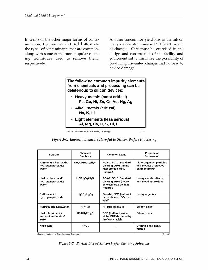
Yield Modeling
Each semiconductor manufacturer has itsown methods for modeling and predictingthe yield of new products, estimating theyield of existing products, and verifying sus-pected causes of yield loss. A variety of yieldmodels, including Murphy's, Poisson's, andSeeds' model, as well as the newer negativebinomial model, can be used to estimateyield from defect density and die size. Incomparison (Figure 3-8), each model has adifferent way of accounting for the distribu-tion of defects on a wafer. The negative bino-mial model accounts for particle clusteringon wafers. Unfortunately, this model is alsoone of the most difficult to use.
Oftentimes, several yield formulas areimplemented within a particular company(e.g., MurphyÕs model for memory, SeedÕsmodel for gate arrays, etc.). Ultimately, eachmodelÕs merit can only be judged by how itperforms when compared to actual yields(i.e., there is no universal model).
For those other than the IC producers, eitherthe standard Murphy model or Seeds modelwill generally suffice. A plot of the Murphymodel (Figure 3-9) shows how a difference indefect density between 0.2 and 0.5defects/cm2, means the difference between a68 percent probe yield and a 40 percentprobe yield, respectively, for a 200mm2
device. Yield is also strongly influenced bydie size. Figure 3-10 simply illustrates theeffect of die size on yield.
To compensate for shortening product life-cycles and drops in device ASPÕs as productsmature, semiconductor manufacturers con-tinually attempt to improve probe yieldsthrough the reduction in defect densities andshrinks of die sizes each generation by 20 per-cent or more. Recently, in response to theplummeting pricing of DRAMs, some manu-facturers have transferred 64M cell designs totheir 16M processes to enable smaller diesizes, higher yields, and reduced manufactur-ing costs. Importantly, however, this savingsis partially off-set by the added complexityassociated with manufacturing the 64M cell,
0.1 1 10
Defect Density x Area
0
0.1
0.2
0.3
0.4
0.5
0.6
0.7
0.8
0.9
1.0
Yie
ld
20132Source: Semiconductor International
Negative Binomial
Seeds 1, Dingwall
Seeds 2
Poisson
Murphy
Figure 3-8. Comparing the Various Yield Models

Yield and Yield Management
INTEGRATED CIRCUIT ENGINEERING CORPORATION3-6
which should increase the cost of manufac-turing these smaller dice. This is graphicallyillustrated in Figure 3-11 which shows threegenerations of 4Mb DRAM designs. Thenumber of chips per wafer increases dramat-ically through each generation.
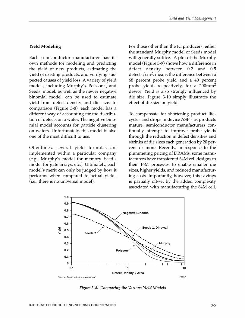
Figure 3-12 shows ICEÕs estimates of 1996defect densities as a function of device tech-nology and feature size. For the mostadvanced fab facilities, defect densities rangebetween 0.3 and 1.2 defects per square cen-timeter, whereas many of the older bipolarlines operate at defect densities as high as 3defects per square centimeter. Figure 3-13shows how the industry has decreaseddefect density as die sizes have increased.Essentially, in the manufacture of todayÕslarge leading-edge chips (0.35µm), less than1.0 defect per square centimeter must beachieved in order to economically producethe devices.
Manufacturers are also improving methodsfor moving new processes from R&D to theproduction floor so that starting yields arehigher, and ultimately, better yield can beaccomplished. A recent study of 16 fabs inthe U.S., U.K., Germany, Japan, and Taiwanby students at the University of California(Berkeley)[2], indicated that fabs starting athigher defect densities rarely achieve betteryields than fabs starting at lower defectlevels (Figures 3-14 and 3-15). Participants ofthe study included AMD, CypressSemiconductor, Delco Electronics, DEC,Intel, IBM, ITT Intermetall, LSI Logic, NEC,Nihon Semiconductor, Oki, Silicon Systems,TSMC, Texas Instruments, and Toshiba.
20 40 60 80 100 120 140 160 180 200 220 240 260 280 300 320 340 360
Def
ect
Den
sity
100
90
80
70
60
50
40
30
20
10
0
YIE
LD
(P
erce
nt)
DIE SIZE (sq mm) 3.002.00
1.501.00
0.50
0.20
0.10
0.05
0.020.01
32 62 93 124 155 186 217 248 279 310 341 372 403 434 465 496 527 558DIE SIZE(thousands of sq mils)
where A = die area in cm2
D = defect density per cm2
y =AD
2
Source: ICE 14444K
1996 4MDRAM
1996 16MDRAM
1996P54CS
1996 64MDRAM
1 – ε –AD
Figure 3-9. MurphyÕs Probe Yield Model (As a Function of Defects per sq. cm)

Yield and Yield Management
INTEGRATED CIRCUIT ENGINEERING CORPORATION 3-7
8 Good DiceOut of 16 = 50%
1 Good DieOut of 4 = 25%
0 Good DieOut of 1 = 0%
7438BSource: ICE
Figure 3-10. Effect of Die Size on Yield
0
1x
2x
ThirdSecondFirst
Source: IBM Journal of R&D 22706
Rat
io o
f C
hip
Per
Waf
er
1
1.28
1.78
Figure 3-11. Chips-Per-Wafer Yield Improvement Across Three Generations of 4Mb DRAM
Yield and Yield Management
INTEGRATED CIRCUIT ENGINEERING CORPORATION3-8
PROCESS TECHNOLOGY (DEFECTS/SQ CM)FEATURE
SIZE(µ)
CMOS14-16
MASKS
ADVANCEDCMOS
18-20 MASKS
ADVANCEDBiCMOS
22 MASKS
BIPOLAR8-10
MASKS
BIPOLAR14-16
MASKS
ADVANCEDBIPOLAR22 MASKS
5.0
2.0
1.5
1.0
0.8
0.5
0.35
—
0.6
0.5
0.4
0.3
—
—
—
—
—
0.3
0.4
0.8
1.0
—
—
0.6
0.7
0.8
1.0
1.2
3
—
—
—
—
—
—
—
2.1
1.2
—
—
—
—
—
—
0.6
0.8
1.0
—
—
14446HSource: ICE
Figure 3-12. Typical 1996 IC Process Defect Levels
DIE SIZE, sq. mils (1,000's)0
0
0
10
20
30
40
50
60
70
80
90
100
PR
OB
E Y
IEL
D, P
ER
CE
NT
6 DEFECTS/cm2
2.5 DEFECTS/cm 1 DEFECT/cm2 2
20
12.9
40
25.8
60
38.7
80
51.6
100
64.5
120
77.4
140
90.3
160
103
MID-1970's
MID-1980's
EARLY1990's
11227D
180
116
200
129
220
142
240
155
MID-1990's
0.75 DEFECT/cm2
Source: ICE
260
168
280
181
300
194
320
207
340
220
LATE1990's
0.35 DEFECT/cm2
DIE SIZE, sq. mm
Figure 3-13. Die Size and Defect Density Trends

Yield and Yield Management
INTEGRATED CIRCUIT ENGINEERING CORPORATION 3-9
F3
F5
F8
F13
F16
7.50
6.005.00
3.00
2.00
1.00
0.50
0.30
0.15
1987 1988 1989
Fab Lines
1990 1991 1992 1993 1994 1995
Def
ect
Den
sity
(fa
tal d
efec
ts p
er s
qu
are
cm)
YearSource: UC Berkeley 21067
Figure 3-14. Defect Densities of 0.7-0.9µm Memory Flows
F2
F4
F6
F8
F9
F12
F15
F16
7.50
6.005.00
3.00
2.00
1.00
0.50
0.30
0.15
1987 1988 1989
Fab Lines
1990 1991 1992 1993 1994 1995
Def
ect
Den
sity
(fa
tal d
efec
ts p
er s
qu
are
cm)
YearSource: UC Berkeley 21068
Figure 3-15. Defect Densities of 0.7-0.9µm Logic Flows

Yield and Yield Management
INTEGRATED CIRCUIT ENGINEERING CORPORATION3-10
Tracking of Random Defects
Wafer fabs routinely track and report ondefect density as a measure of manufactur-ing excellence. In many cases, however, thedefect densities reported are simply calcula-tions based on historical wafer probe yieldinformation. While this may be an adequatestarting point, the real challenge is to makeimprovements in these numbers as effi-ciently as possible. In order to accomplishthis, the fab engineer needs to identify thespecific process steps, pieces of equipment,input materials, etc. that are the major con-tributors to the defect density.
Many organizations are beginning to adopt amethodology called defect budgeting as ameans to narrow down the search forsources of random defects in the process.The methodology involves the constructionof a detailed process flow diagram for iso-lated segments of the process and the use ofvarious problem solving tools to tie the total
defects measured at the end of the processsequence to the likely sources in the processflow. An example of one of these diagrams isshown in Figure 3-16. The constituents thatcarry random defects into the process willvary widely according to the type of processbeing mapped. For example, for one processstep there may be several different inputmaterials to consider and no additional com-ponents, while others may be equipmentintensive with very little in the way of defectcontribution from input materials or compo-nents. All of these factors must be consid-ered when constructing the map. Thesedefect process maps are most effective whenused for a small section of the total processflow. The areas to be investigated are estab-lished using Pareto diagrams of randomdefect occurrence.
Input Materials
Components
Defects FromPrevious
Operations
EnvironmentProcess
Equipment
Σ (Defects) Σ (Defects)
Data
Defect Analysis
To Next Operation
OperationA
OperationB
RandomDefect
Measurementand
Analysis
EnvironmentProcess
Equipment
Input Materials
Components
Source: ICE 22794
Figure 3-16. Defect Budget Process Map

Yield and Yield Management
INTEGRATED CIRCUIT ENGINEERING CORPORATION 3-11
Problem solving tools that are generally usedduring the process in addition to Pareto dia-grams are Cause and Effect diagrams, andseveral methods of statistically designedexperiments. Also necessary are publishedinformation by equipment suppliers, relatedtechnical publications, and sophisticatedmetrology tools designed to detect randomdefects. The trend is for these all to be com-bined into a systematic yield managementsystem. These will be discussed in moredepth later in this section.
Once this diagram is completed, prioritiesmay be established to take action on majorcontributors to the defect rate in a more effi-cient manner. The continuous effort toreduce defect densities is critical to the fabfor numerous reasons.
First, there is the issue of maintaining a com-petitive wafer cost. This will be illustrated inthe section on benchmarking by looking atcomparisons of defect density versus waferand die cost.
Secondly, there is the need to prepare for thenext generations of parts with higher devicedensities and probably larger wafers.
Third, there is the effect of defect densities oncycle time and product output. For any inputwafer level capacity for the fab, the antici-pated output and corresponding cycle timedepend greatly on defect density. To estimatethe effect on cycle time, making the assump-tion that a modern fab is basically reworkfree, the baseline cycle time must be multi-plied by the reciprocal of the first time yield.The first time yield can then be expressed asa function of defect density by substitutingone of the yield model formulas (Murphy,Seeds, etc.). Assuming an input limit of20,000 wafers per month, the effective output
capacity is drastically reduced as the defectdensity increases. A quick calculation showsthat cycle time rapidly increases as defectdensities increase since more time must beexpended to satisfy any constant outputrequirement. This obviously can have amajor impact on the total equipment setneeds for the fab.
Metrology Tools: Tying Contamination toYield
In the fab, patterned and unpatterned waferinspection systems allow accurate identifica-tion of defects on wafers. However, thesesystems currently include no method forclassifying the defects into "killer" and harm-less defects. In addition, past interfacesbetween these inspection systems with probeyield and off-line metrology tools (i.e., SEMs,FIBs) was limited by the inability to managethe large volume of data created by thesesystems by fabs operating 24 hours a day, 7days a week. However, sophisticated soft-ware tools are now making it feasible tobuild facility-wide information systems tocollect, store, and analyze valuable yieldmanagement data from many sources in thefab and/or assembly operations.
The data required for yield managementincludes parametric test and functionalprobe from the test floor, process data fromthe fab equipment, in-line monitoring datafrom patterned wafer inspection systems,and work-in-process (WIP) data from the fac-tory floor management system. Patternedwafer inspection systems, using both laser-based inspection systems (by Tencor andInspex) as well as white-light inspection sys-tems with digital image processing (manu-factured by KLA) are available for in-linemonitoring of defects. These systems, whichhave been used in fabs for several years, have
Yield and Yield Management
INTEGRATED CIRCUIT ENGINEERING CORPORATION3-12
only recently become capable of real-timeprocessing of the enormous amount of defectdata generated in the monitoring process.
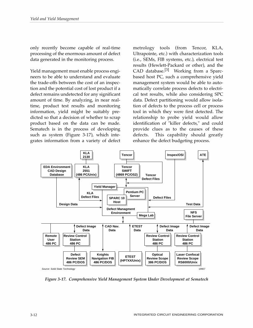
Yield management must enable process engi-neers to be able to understand and evaluatethe trade-offs between the cost of an inspec-tion and the potential cost of lost product if adefect remains undetected for any significantamount of time. By analyzing, in near real-time, product test results and monitoringinformation, yield might be suitably pre-dicted so that a decision of whether to scrapproduct based on the data can be made.Sematech is in the process of developingsuch as system (Figure 3-17), which inte-grates information from a variety of defect
metrology tools (from Tencor, KLA,Ultrapointe, etc.) with characterization tools(i.e., SEMs, FIB systems, etc.), electrical testresults (Hewlett-Packard or other), and theCAD database.[3] Working from a Sparc-based host PC, such a comprehensive yieldmanagement system would be able to auto-matically correlate process defects to electri-cal test results, while also considering SPCdata. Defect partitioning would allow isola-tion of defects to the process cell or processtool in which they were first detected. Therelationship to probe yield would allowidentification of "killer defects," and couldprovide clues as to the causes of thesedefects. This capability should greatlyenhance the defect budgeting process.
KLA2130
Tencor Inspex/OSI ATE
EDA EnvironmentCAD Design
Database
KLA2551
(486 PC/Unix)
TencorSWIFT
(4869 PC/OS2)
Yield Manager
Mega LabNFS
File Server
RemoteUser
486 PC
Review ControlStation486 PC
Review ControlStation486 PC
Review ControlStation486 PC
DefectReview SEM486 PC/DOS
KnightsNavigation FIB
486 PC/DOS
ETEST(HP7XX/Unix)
OpticalReview Scope386 PC/DOS
Laser ConfocalReview ScopeRS6000/Unix
TencorDefect Files
Design Data
KLADefect Files
Defect ManagmentEnvironment
Defect Files
Test Data
Defect ImageData
CAD Nav.Data
ETESTData
Defect ImageData
Defect ImageData
Source: Solid State Technology 19907
Pentium PCServer
SPARC 10Host
Figure 3-17. Comprehensive Yield Management System Under Development at Sematech

Yield and Yield Management
INTEGRATED CIRCUIT ENGINEERING CORPORATION 3-13
As we reviewed in Chapter 1, yield dependson defect density. It is also generallyaccepted that at least 50 percent of yield lossin fabs is due to random defects, in otherwords, contamination at the wafer surface.However, despite this relationship, methodsfor directly correlating yield and device per-formance to actual contamination levels ispractically non-existent.[2] In addition, yieldis always going to be a function of the deviceand its associated process. As new fabs tacklethe challenges associated with characterizingprocesses for sub-0.5mm processing, manytraditional laboratory tools typically used forfailure analysis and device characterizationmay become attractive for in-line defectmonitoring (Figure 3-18).
Process Capability and the Role of SPC
Comprehensive yield management in a fabwould ideally include the automated collec-tion of data from multiple sources (bothprocess equipment and monitoring tools),feedback to a common source for real-timeanalysis, automatic classification as toimpact on yield and cause of defect, andrapid elimination of yield-limiting problems.Yield improvement would be driven by theability to continually improve process capa-bility, while decreasing defect density at eachmajor process tool. In reality, however, mostexisting fabs have neither the sophisticatedsoftware solutions nor the workstationsneeded to process the data and implementsuch real-time yield management. In addi-tion, the methods for directly correlatingyield and device performance to actual cont-amination levels are scarce, although compa-nies including Texas Instruments, Tencor,KLA, Hewlett-Packard, and others, aredeveloping these capabilities.
Another major factor controlling line andprobe yields is the ability of the fab to controlprocess variations on critical parameters. Inmany progressive fabs, situational StatisticalProcess Control (SPC) is now becoming morepopular as engineers concentrate more oncritical processes and avoid the temptation tooveruse tools such as process control charts.
Although there are a variety of tools avail-able to the process engineer to assist inmaking statistically valid decisions with asmall amount of data, the most usefulStatistical Process Control tools in the fab are:
¥ Process Capability Analysis¥ Process Control Charts ¥ Measurement System Analysis
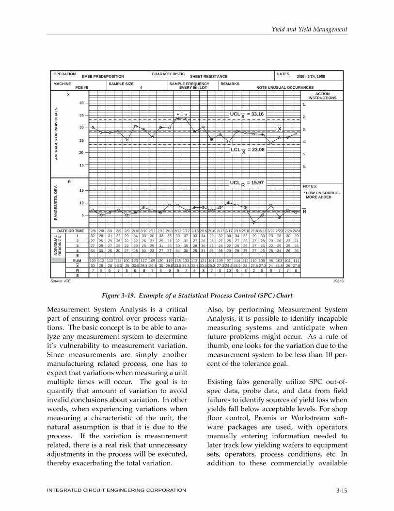
Care must be exercised, however, that theusefulness of these tools is directly related tothe ability of the engineer to apply them cor-rectly to specific applications. As an exam-ple, consider the case of Variable ControlCharts and their applicability to fab opera-tions. Figure 3-19 shows a classical variablecontrol chart form applied to sheet resistancevalues from a diffusion operation. The X bar,R chart shown in the figure was originallydeveloped in the 1920Õs by Shewhart andwas intended to track a continuous flowmanufacturing process that produces largequantities of identical product. In our appli-cation in the fab, the process is more batchoriented and the target values might varyfrom batch to batch. Therefore, the samplingplans, frequency of sampling, control limitcalculations need to be modified to accountfor the possibility that several families ofvariation could exist and that the chartshould be sensitive to all of those possibili-ties. That is why new control chart types,such as the Roberts Chart, have been devel-oped. More and more of these charts are

Yield and Yield Management
INTEGRATED CIRCUIT ENGINEERING CORPORATION3-14
being commented on in the literature and thecreative process engineer should be on the
alert looking for adjustments in the tools thatreflect changes in process technology.
Figure 3-18. Likely Evolution of Problem-Solving Tools for Increasingly Complex Devices
Process AnalysisWafer Fab Technology
Microstructure and Microtopography
Composition andPhase Identification
Residues andOrganics
Microcontamination
Particle Analysis
Mechanical Behavior
Critical Dimensions
Film Thicknessand Roughness
Defects Metrology
LaB6 50Å SEM120keV 3Å TEM
0.5-1.0µm SEM-EDX2000Å AES10 µm 02 & Cs SIMSmm XRFX-ray & Electron Diffraction
AESO2 & Cs SIMSFTIR
SIMS
SEM-EDXFTIRAESOptical Fluorescence
Empirical Observation
Stress Measurements Of Thin FilmsBy Measurement Of Wafer Bow
LaB6 Source SEM
Optical InterferometryEllipsometryFilm ResistivityProfilometry
Optical Defect Inspection Tools
20Å FESEM200keV 1.8Å TEMAFM & STM
0.3-1.0µm SEM Low-Z EDX80Å TEM, Low-Z EDX2000Å AES100 µm XRFX-ray DiffractionSmall Area Electron Diffraction
AES, ESCATOF SIMS10µm FTIR & RAMAN
TXRFVPD-GFAAVPD-ICP-AESO2 & Cs SIMS
SEM, Low-Z EDXAESFTIRRAMANOptical Fluorescence
Microindentor for Stress-Strain andMicrohardness Measurements ofThin FilmsDirect Measurement of Stress in<1.0 µm Lines by X-ray Diffraction
<2keV FESEM
Optical InferometryEllipsometryXRF Direct MeasurementAFM & STM Profilometry
Optical Tools Computer Linked ToLaB6 SEM, Low-Z EDX (AutomaticParticle Coordinate Transfer andSteering to Analysis Area, ImageSpectral Acquisition with DigitalStorage)
Immersion Lens 8Å FESEMHigh Voltage or FETEMAFM & STM
0.3-1.0µm SEM, Low-Z EDZ80Å TEM, Low-Z EDX<500Å FEAES100µm Low-Z XRFX-ray DiffractionSmall Area Electron Diffraction
AES, ESCATOF SIMS10-1.0µm FTIR & RAMAN
TXRFVPD-GFAAVPD-ICP-MSNew SIMS (TOF, Post Ionization,Accelerator, <500Å Ga)
SEM, Low-Z EDXFEAESFIB With Ga SIMSFTIRRAMANOptical Fluorescence
Microindentor for Stress-Strain andMicrohardness Measurements ofThin FilmsDirect Measurement Of Stress in<1.0µm Lines by X-ray Diffraction
<2keV Immersion Lens FESEM
Optical InterferometryEllipsometryXRF Direct MeasurementAFM & STM Profilometry
Optical Tools, et al., Computer Linkedto FESEM, Low-Z EDX et al (Auto-matic Particle Coordinate Transferand Steering to Analysis Area, FullyAutomated Analysis and Reporting)
1.0µm 0.7-0.8µm 0.4-0.6µm
Legend:AES - Auger Electron SpectroscopyAFM - Atomic Force MicroscopyEDX - Energy Dispersive X-rayESCA - Electrospectroscopy For Chemical
AnalysisFEAES - Field Emission AESFESEM - Field Emission SEMFETEM - Field Emission TEM
FIB - Focused Ion BeamFTIR - Fourier Transform Infraredlow z - Light Or Low ElementRAMAN - Raman Optical SpectroscopySEM - Scanning Electron MicroscopySIMS - Secondary Ion Mass SpectroscopySTM - Scanning Tunneling MicroscopyTEM - Transmission Electron Microscopy
TOF SIMS - Time Of Flight SIMSTXRF - Total Reflection XRFVPD-GFAA - Vapor Phase Decomposition, Graphite
Furnace Atomic AbsorptionVPD-ICP/AES - VPD-ICP - Auger Electron SpectroscopyVPD-ICP/MS - VPD Inductively Coupled Plasma,
Mass SpectroscopyXRF - X-ray Fluorescence
Source: Semiconductor International 19909
Yield and Yield Management
INTEGRATED CIRCUIT ENGINEERING CORPORATION 3-15
Measurement System Analysis is a criticalpart of ensuring control over process varia-tions. The basic concept is to be able to ana-lyze any measurement system to determineitÕs vulnerability to measurement variation.Since measurements are simply anothermanufacturing related process, one has toexpect that variations when measuring a unitmultiple times will occur. The goal is toquantify that amount of variation to avoidinvalid conclusions about variation. In otherwords, when experiencing variations whenmeasuring a characteristic of the unit, thenatural assumption is that it is due to theprocess. If the variation is measurementrelated, there is a real risk that unnecessaryadjustments in the process will be executed,thereby exacerbating the total variation.
Also, by performing Measurement SystemAnalysis, it is possible to identify incapablemeasuring systems and anticipate whenfuture problems might occur. As a rule ofthumb, one looks for the variation due to themeasurement system to be less than 10 per-cent of the tolerance goal.
Existing fabs generally utilize SPC out-of-spec data, probe data, and data from fieldfailures to identify sources of yield loss whenyields fall below acceptable levels. For shopfloor control, Promis or Workstream soft-ware packages are used, with operatorsmanually entering information needed tolater track low yielding wafers to equipmentsets, operators, process conditions, etc. Inaddition to these commercially available
OPERATION CHARACTERISTIC DATES
MACHINE SAMPLE SIZE SAMPLE FREQUENCY REMARKS
ACTIONINSTRUCTIONS
1.
2.
3.
4.
5.
6.
NOTES:
X
AV
ER
AG
ES
OR
IND
IVID
UA
LS
R
RA
NG
ES
/ST
D. D
EV
.
DATE OR TIME
IND
IVID
UA
LR
EA
DIN
GS 1
2345
SUMXRS
19846Source: ICE
BASE PREDEPOSITION SHEET RESISTANCE 2/80 - 2/24, 1988
FCE #5 4 EVERY 5th LOT NOTE UNUSUAL OCCURANCES
40
35
30
25
20
15
15
10
5
2/8 2/8 2/9 2/9 2/10 2/10 2/11 2/11 2/11 2/12 2/12 2/15 2/16 2/16 2/17 2/17 2/18 2/18 2/19 2/22 2/22 2/23 2/24 2/242/932 28 31 32 34 33 30 33 35 39 37 33 34 29 32 30 34 33 29 30 29 28 30 292927 25 29 26 32 26 27 29 31 32 31 27 26 25 27 25 27 28 27 28 20 26 23 312227 29 27 25 29 25 25 31 26 30 35 28 30 22 24 22 25 26 27 26 22 25 25 262234 30 25 30 28 33 23 27 27 34 30 25 31 25 26 20 28 25 27 25 25 24 26 2527
120 112 112 113 123 117 105 120 119 135 133 113 121 101 109 97 114 112 110 109 96 103 104 11110030 28 28 28.3 30.8 29.3 26.3 30 29.8 33.8 33.3 28.3 30.3 25.3 27.3 24.3 28.5 28 27.5 27.3 24 25.8 26 27.8257 5 6 7 6 8 7 6 9 9 7 8 8 7 8 10 9 8 2 5 9 7 7 65
LOW ON SOURCE -MORE ADDED
*
UCL X = 33.16
LCL X = 23.08
X
UCL R = 15.97
R
* *
Figure 3-19. Example of a Statistical Process Control (SPC) Chart

Yield and Yield Management
INTEGRATED CIRCUIT ENGINEERING CORPORATION3-16
solutions, many manufacturers have devel-oped proprietary solutions for yield manage-ment and shop floor control (controllingwork-in-process (WIP), inventory and equip-ment). They might also have proprietarymethods for achieving a certain level of in-line defect monitoring.
When new equipment is brought into thefab, its operations are characterized for eachdevice manufactured in that facility.Statistical techniques should be used torelate process variations to yield. From thatinitial analysis, key parameters are selectedfor process monitoring and for process capa-bility analysis.
Histograms can be constructed to verify nor-mality as part of the process capability studyand is intended to ensure that processes withonly random effects are quantified in thestudy. For example, a histogram of sheet resis-
tance is shown in Figure 3-20. Since the defi-nition for process capability is the distancebetween -3s and +3s around the mean, asimple calculation using a reasonable samplesize will quantify the amount of variation inthe process under investigation.
To evaluate the calculated process capabilityversus fab requirements, the process engi-neer will normally use Process CapabilityIndices such as Cp and Cpk. These indicesare figures of merit that describe the processvariation in terms of it relationship to a set ofspecifications. The objective is to have aprocess capability index as large as possiblewhich indicates that the total process varia-tion is considerably smaller than the specifi-cation it is intended to satisfy. Figure 3-21illustrates the relationship between processvariation and process capability indices for agiven specification. Also included are theformulae for Cp and Cpk for comparison.
FR
EQ
UE
NC
Y
50
40
30
20
10
012 12.5 13 13.5 14 14.5 15 15.5 16 16.5 17 17.5
POLY SHEET RESISTANCE, OHMS/SQUARE
CMOS III A, REV. C, STEP 12.2
FURN. 4C
N = 220
X = 14.46
19847Source: ICE
Figure 3-20. A Typical Histogram Shows the Distribution Around a Target Value

Yield and Yield Management
INTEGRATED CIRCUIT ENGINEERING CORPORATION 3-17
The use of SPC data for continuousimprovement in a semiconductor manufac-turing environment has become hamperedby the increasing volume of data producedat each process step. One must focus on theimportant measurements (determiningwhich measurements are key to productquality). Typically, engineers analyze defectdistributions, constructing Pareto charts that
plot the reasons for failures versus the fre-quency of occurrence. Then the defect istraced back to any number of causes (i.e., ifthe problem is shorts, SEM and FIB analysisamong elemental SIMS or other analyzesmight be used to identify the culprit). Dataallows tracing to the specific tools, recipe, set-up, operator, etc., along with PM schedules.
Case 1
Cp = 1Cpk = 1
Case 2
Cp = 2Cpk = 1
Case 3
Cp = 2Cpk = 2
USL
USL
USL
LSL
LSL
LSL
–3σ +3σ
–3σ +3σ
–3σ +3σ
Source: ICE 22795
Cp =USL – LSL
Process Capability
USL – LSL
6σ=
Cpk = Cp (1 – k)
Where k =[Mean – Nominal]
1/2 Total Specification
µ
µ
Figure 3-21. Relationship Between Cp and Cpk

Yield and Yield Management
INTEGRATED CIRCUIT ENGINEERING CORPORATION3-18
Ultimately, the product yield is affected notonly by the processing and testing of thechip, but also the original design. While athorough discussion of EDA capabilities isbeyond the scope of this book, suffice it tosay that many companies are interested intying yields and process data back to theoriginal design.
Yield Data Management Systems
As the need for more data relevant to makingimprovements in line and probe yieldsbecomes more acute due to the tremendousleverage of yield on manufacturing costs(and therefore profits), another potentialproblem is created. The extremely largeamount of data now available for this pur-pose needs to be managed in a systematicway to ensure the efficient implementationof improvement programs.
To this end, organizations have tried toadopt data management systems to assist inthis task. Some fabs have taken theapproach of developing their own internalproprietary systems to coordinate the datagenerated by analysis tools. To a largedegree, this was necessary due to the lack ofstandards utilized by the metrology manu-facturers, and to the lack of commerciallyavailable systems for managing this type ofdata. The degree of success realized throughthis approach has been directly correlatableto the internal resources available to theinterested organizations.
As an example, Intel has had success inapplying the ÒTheory of ConstraintsÓ con-cepts presented in the 1993/1994 time framein papers by Menon and Sohn to fab lineyields. The model allows for the establish-ment of individual operation scrap goals
based on an overall line yield goal. Figure 3-22 illustrates a table of individual process stepgoals within a cluster, along with actual per-formance and focal areas for improvement.
In the recent past, several alliances havebeen formed to attempt to integrate theactual data being generated into a yieldimprovement methodology. One exampleof this type of effort is the formation of theYield Management Team (YMT) which hasmembers from several companies represent-ing metrology hardware, wafer probe equip-ment, and software solutions. The teamincludes Advantest Corp., Electroglas Corp.,Keithley Instruments, Knights Technology,SVR, and riant Technologies Inc.
The goal of YMT is to work on improvingtechnical equipment and software interfacesand develop new technologies, and then tryto select the best combination of equipmentand software for individual fab requirements.
ClusterToolset
ScrapGoal
WeeklyScrap
DeltaFocusAreas
M. Etch
Planar
Sputter
Diff:FE
Gold
WAMO
AMAT
Diff:BE
WJ
LRC
Litho
Implant
AWS
Total
27
9
31
186
3
10
24
3
6
70
130
56
145
700
250
52
64
210
10
9
23
—
2
54
101
26
66
867
(223)
(43)
(33)
(24)
(7)
1
1
3
4
16
29
30
79
167
M. Etch
Planar
Sputter
Diff:FE
Gold
Source: Intel 22796
Figure 3-22. Hypothetical Weekly Scrap Targets

Yield and Yield Management
INTEGRATED CIRCUIT ENGINEERING CORPORATION 3-19
Figure 3-23 represents how a fab might inte-grate the in-line data generation, analysis,and end of line test data into a centralized,rational data base.[4]
References
1. W. Kern, Òhandbook of SemiconductorWafer Cleaning Technology,Ó NoyesPublications, New Jersey, 1993
2. R. Leachman, ÒThe CompetitiveSemiconductor Manufacturing Survey:Third Report,Ó UC Berkeley, August 15,1996
3. P. Proctor, ÒSematech Develops Softwarefro Yield Enhancement, DefectTracking,Ó Solid State Technology,December 1994
4. S. Smith et.al., ÒRapid yield LearningThrough Data Integration,Ó SemiconductorInternational, June/July 1996
Laser ConfocalReview
Sort Data(Direct from Tester)
Bitmap Data
Lot EquipmentHistory
SPC
X-WindowUser Access
(Power Mac/NCD)
Data OutExport to Excel
Image DBAuto Defect
Classification
Optical Review
SEMw/EDS Review
KLA Optical Detection
Tencor Patterned Detection
Yield Management System(Knights Technology)
AnalysisApplication
Defect AnalysisElectrical CorrelationDefect Image Search
Yield Prediction
Defect DB
Unpatterned Wafer Inspection/Defect Review(Photo/Etch Engineering - Metrology Group)
Source: Motorola/Semiconductor International 22797
CAD NavigationNetwork
Device Lab
FIBSEMI w/EDS
Bit Scope
OpticalMicroscope
MetrologySEMs
TencorUnpatterned
Figure 3-23. MOS-13 Defect Management System

Yield and Yield Management
INTEGRATED CIRCUIT ENGINEERING CORPORATION3-20