XSV Board 1.0 – HDL Interfaces and Example Designs 10/100...
21
XSV Board 1.0 – HDL Interfaces and Example Designs 10/100 Mbps Ethernet MAC VLSI Research Group Electrical Engineering Bandung Institute of Technology , Bandung, Indonesia Last Modified: 20 September 2001 Bandung Institute of Technology 1. About the Design Ethernet is one of LAN technology, which is most widely used to make computer network. Ethernet MAC is a part of Ethernet device, which control transmitting and receiving data packet based on CSMA/CD protocol. Ethernet MAC consists of two part, the transmitter and the receiver. The transmitter encapsulates data into data packet dan controls data sending. The receiver decapsulates data and controls data receiving. In OSI communication model, Ethernet MAC is included in data link layer. This 10/100 Mbps Ethernet MAC was implemented in Virtex XCV300-4- PQ240 FPGA, which is included in XSV board. Further implementation is needed to make it work specifically for a full duplex switched network, which needs MII Management Module and MAC Control Module. There is support to read and write to RAM from the PC via the parallel port as well, for debugging and tests purposes (this maybe easily removed). Thanks for James Brennan from School of Computer Science and Electrical Engineering, University of Queensland, who gave permission to use PC to SRAM interface. 2. Description of the Design Design Overview This HDL design is an implementation of an 10/100 Mbps Ethernet MAC. The Ethernet MAC was designed and built on an XSV-300 board (version 1.0) from the XESS Corp. (http://www.xess.com ) using Xilinx Foundation 3.1i and associated tools to make the design. The board makes use of an LXT970A Ethernet Transceiver (PHY) from Level One (an Intel company) to encode and decode the signals onto a 100 Mbps full duplex twisted pair switched network. (The chip has been forced to 100 Mbps operation and can be changed by reprogramming the CPLD, however this means much of the code will need to be rewritten – see Design Limitations in Design Considerations for more information).
Transcript of XSV Board 1.0 – HDL Interfaces and Example Designs 10/100...
XSV Board 1.0 – HDL Interfaces and Example Designs
10/100 Mbps Ethernet MAC VLSI Research Group
Electrical Engineering
Bandung Institute of Technology, Bandung, Indonesia Last Modified: 20 September 2001 Bandung Institute of Technology
1. About the Design
Ethernet is one of LAN technology, which is most widely used to make computer network. Ethernet MAC is a part of Ethernet device, which control transmitting and receiving data packet based on CSMA/CD protocol. Ethernet MAC consists of two part, the transmitter and the receiver. The transmitter encapsulates data into data packet dan controls data sending. The receiver decapsulates data and controls data receiving. In OSI communication model, Ethernet MAC is included in data link layer. This 10/100 Mbps Ethernet MAC was implemented in Virtex XCV300-4-PQ240 FPGA, which is included in XSV board. Further implementation is needed to make it work specifically for a full duplex switched network, which needs MII Management Module and MAC Control Module. There is support to read and write to RAM from the PC via the parallel port as well, for debugging and tests purposes (this maybe easily removed). Thanks for James Brennan from School of Computer Science and Electrical Engineering, University of Queensland, who gave permission to use PC to SRAM interface. 2. Description of the Design
Design Overview This HDL design is an implementation of an 10/100 Mbps Ethernet MAC. The Ethernet MAC was designed and built on an XSV-300 board (version 1.0) from the XESS Corp. (http://www.xess.com) using Xilinx Foundation 3.1i and associated tools to make the design. The board makes use of an LXT970A Ethernet Transceiver (PHY) from Level One (an Intel company) to encode and decode the signals onto a 100 Mbps full duplex twisted pair switched network. (The chip has been forced to 100 Mbps operation and can be changed by reprogramming the CPLD, however this means much of the code will need to be rewritten – see Design Limitations in Design Considerations for more information).

Design Structure 10/100 Mbps Ethernet MAC consists of two parts, the transmitter and the receiver (see Figure 1). In OSI communication model, Ethernet MAC is included in data link layer. The functions of 10/100 Mbps Ethernet MAC are :
• Connecting physical layer with network layer in transferring data process
• Packeting data in used data packet format (in this design, we use IEEE 802.3 standard data packet format)
• Detecting error in received data packet • Control data flow in Ethernet Network Interface Card
Figure 1. 10/100 Mbps Ethernet MAC design
3. Modules Descriptions
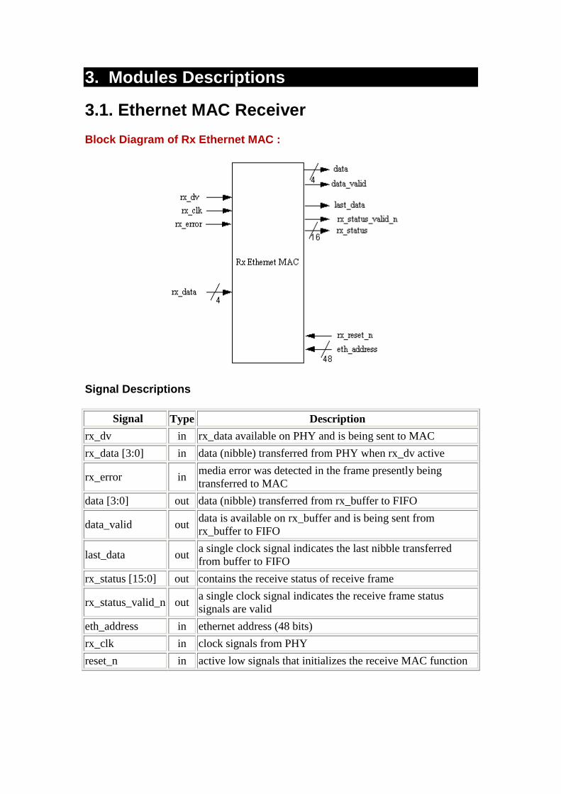
3.1. Ethernet MAC Receiver Block Diagram of Rx Ethernet MAC :
Signal Descriptions
Signal Type Description rx_dv in rx_data available on PHY and is being sent to MAC rx_data [3:0] in data (nibble) transferred from PHY when rx_dv active
rx_error in media error was detected in the frame presently being transferred to MAC
data [3:0] out data (nibble) transferred from rx_buffer to FIFO
data_valid out data is available on rx_buffer and is being sent from rx_buffer to FIFO
last_data out a single clock signal indicates the last nibble transferred from buffer to FIFO
rx_status [15:0] out contains the receive status of receive frame
rx_status_valid_n out a single clock signal indicates the receive frame status signals are valid
eth_address in ethernet address (48 bits) rx_clk in clock signals from PHY reset_n in active low signals that initializes the receive MAC function
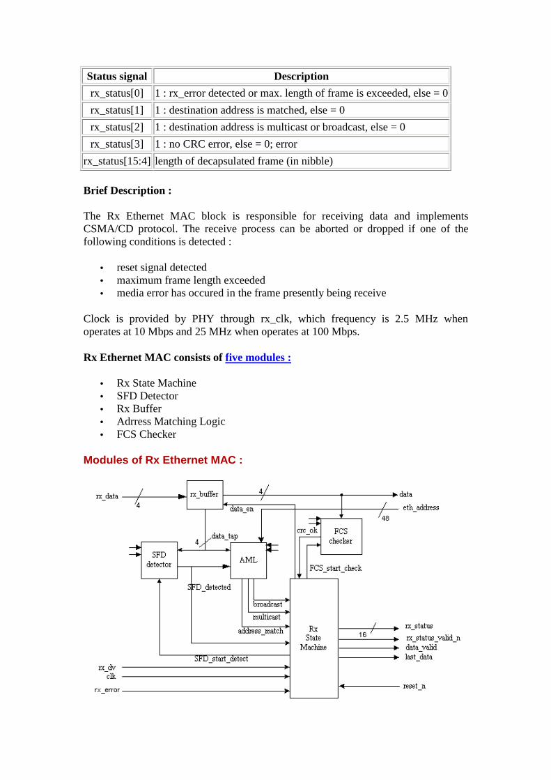
Status signal Description rx_status[0] 1 : rx_error detected or max. length of frame is exceeded, else = 0 rx_status[1] 1 : destination address is matched, else = 0 rx_status[2] 1 : destination address is multicast or broadcast, else = 0 rx_status[3] 1 : no CRC error, else = 0; error
rx_status[15:4] length of decapsulated frame (in nibble)
Brief Description :
The Rx Ethernet MAC block is responsible for receiving data and implements CSMA/CD protocol. The receive process can be aborted or dropped if one of the following conditions is detected :
• reset signal detected • maximum frame length exceeded • media error has occured in the frame presently being receive
Clock is provided by PHY through rx_clk, which frequency is 2.5 MHz when operates at 10 Mbps and 25 MHz when operates at 100 Mbps.
Rx Ethernet MAC consists of five modules :
• Rx State Machine • SFD Detector • Rx Buffer • Adrress Matching Logic • FCS Checker
Modules of Rx Ethernet MAC :
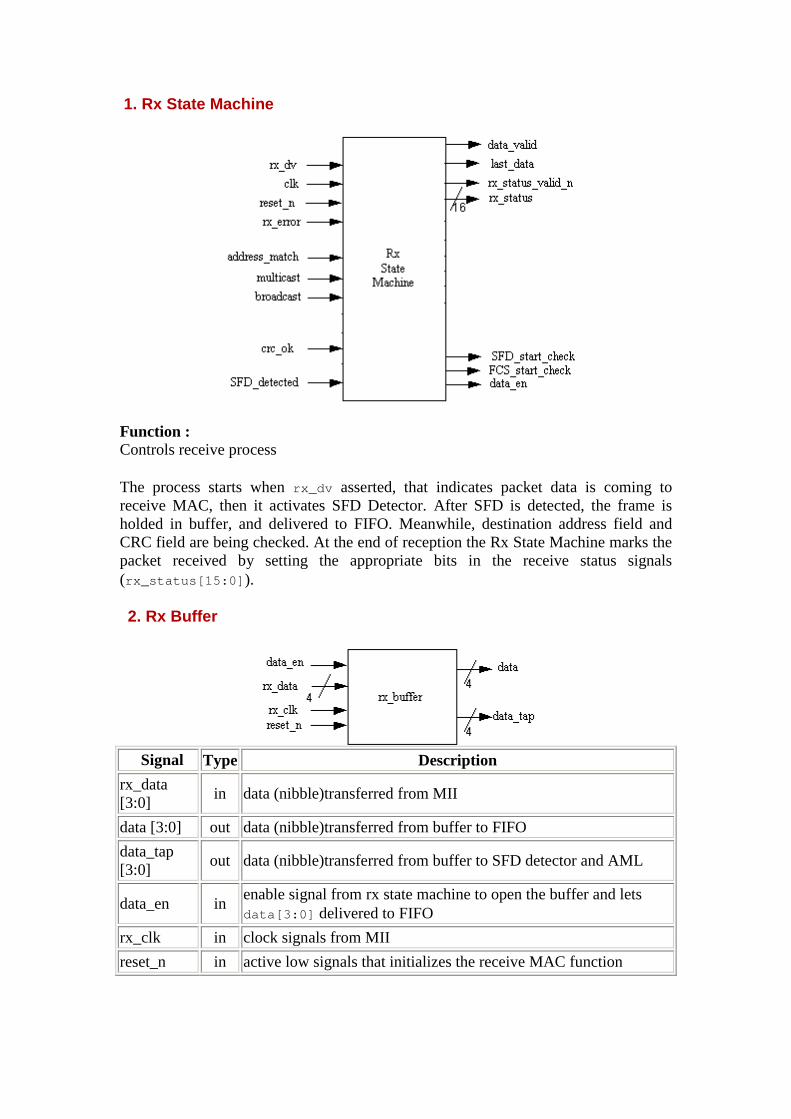
1. Rx State Machine
Function : Controls receive process
The process starts when rx_dv asserted, that indicates packet data is coming to receive MAC, then it activates SFD Detector. After SFD is detected, the frame is holded in buffer, and delivered to FIFO. Meanwhile, destination address field and CRC field are being checked. At the end of reception the Rx State Machine marks the packet received by setting the appropriate bits in the receive status signals (rx_status[15:0]).
2. Rx Buffer
Signal Type Description
rx_data [3:0] in data (nibble)transferred from MII
data [3:0] out data (nibble)transferred from buffer to FIFO data_tap [3:0] out data (nibble)transferred from buffer to SFD detector and AML
data_en in enable signal from rx state machine to open the buffer and lets data[3:0] delivered to FIFO
rx_clk in clock signals from MII reset_n in active low signals that initializes the receive MAC function

Function : Holds the frame being received, before they transferred to FIFO.
It lets data_tap[3:0] delivered to SFD detector and AML all time, and delivered data_tap[3:0] when data_en is active (after SFD detected). This makes frame decapsulated.
3. SFD Detector
Signal Type Description
SFD_start_detect in a single clock signals gives instruction to SFD detector to begin to detect the SFD
data [3:0] in data (nibble) transferred from MII SFD_detected out this signal indicates that SFD has detected. rx_clk in clock signals from MII reset_n in active low signals that initializes the receive MAC function
Function : Detects Start Frame Delimiter (SFD) that indicates the start of frame to be received.
It is activated by SFD_start_check signal from Rx State Machine that launched after rx_dv asserted. When the SFD detected, SFD Detector launches SFD_detected.
4. Address Matching Logic (AML)
Signal Type Description eth_address [47:0] in ethernet address
SFD_detected in signal from SFD detector, means: be ready to check the destination address
data_tap [3:0] in nibbles from buffer (destination address)
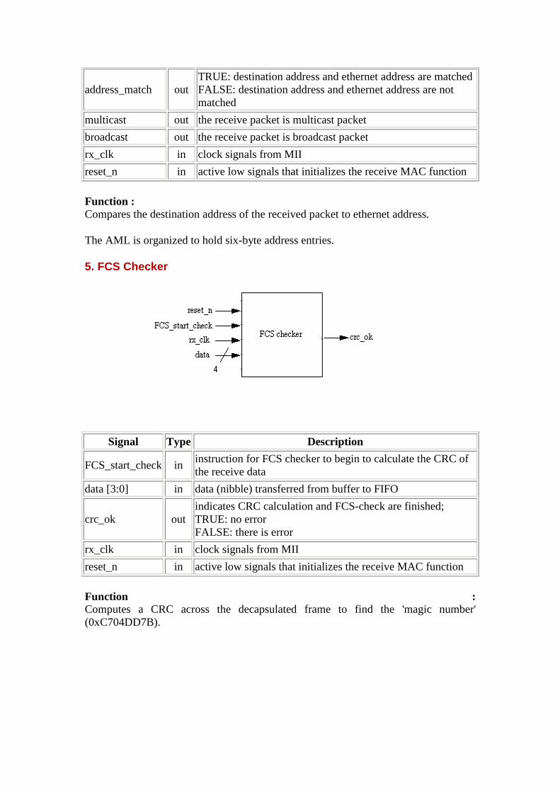
address_match out TRUE: destination address and ethernet address are matchedFALSE: destination address and ethernet address are not matched
multicast out the receive packet is multicast packet broadcast out the receive packet is broadcast packet rx_clk in clock signals from MII reset_n in active low signals that initializes the receive MAC function
Function : Compares the destination address of the received packet to ethernet address.
The AML is organized to hold six-byte address entries.
5. FCS Checker
Signal Type Description
FCS_start_check in instruction for FCS checker to begin to calculate the CRC of the receive data
data [3:0] in data (nibble) transferred from buffer to FIFO
crc_ok out indicates CRC calculation and FCS-check are finished; TRUE: no error FALSE: there is error
rx_clk in clock signals from MII reset_n in active low signals that initializes the receive MAC function
Function : Computes a CRC across the decapsulated frame to find the 'magic number' (0xC704DD7B).

3.2. Ethernet MAC Transmitter
Block Diagram of Tx Ethernet MAC :
Brief Description :
TxEthMAC implements CSMA/CD protocol when transmiting packets of data. Before transmiting packets of data, TxEthMAC must assure that medium is idle and then monitors medium continuously if there is a collision in the middle of transmit process. If collision happened, TxEthMAC makes backoff operation and retries to transmit after a random period depends on number of collision attempt. The transmit process can be aborted or dropped if one of the following conditions is detected :
• excess deferral, occurs when TxEthMAC can't get opportunity to transmit longer than twice maximum length of Ethernet frame
• late collision, occurs when collision is detected after 512 bits of data has been transmited
• excessive collision, occurs when collision is detected more than 15 times • underrun, occurs when host can't provide nibbles of data for transmit operation • excessive length, occurs when the length of packet is longer than 1518 bytes
Clock is provided by MII through tx_clk, which frequency is 2.5 MHz when operates at 10 Mbps and 25 MHz when operates at 100 Mbps.
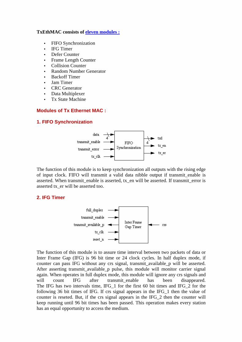
TxEthMAC consists of eleven modules :
• FIFO Synchronization • IFG Timer • Defer Counter • Frame Length Counter • Collision Counter • Random Number Generator • Backoff Timer • Jam Timer • CRC Generator • Data Multiplexer • Tx State Machine
Modules of Tx Ethernet MAC :
1. FIFO Synchronization
The function of this module is to keep synchronization all outputs with the rising edge of input clock. FIFO will transmit a valid data nibble output if transmit_enable is asserted. When transmit_enable is asserted, tx_en will be asserted. If transmit_error is asserted tx_er will be asserted too.
2. IFG Timer
The function of this module is to assure time interval between two packets of data or Inter Frame Gap (IFG) is 96 bit time or 24 clock cycles. In half duplex mode, if counter can pass IFG without any crs signal, transmit_available_p will be asserted. After asserting transmit_available_p pulse, this module will monitor carrier signal again. When operates in full duplex mode, this module will ignore any crs signals and will count IFG after transmit_enable has been disappeared. The IFG has two intervals time, IFG_1 for the first 60 bit times and IFG_2 for the following 36 bit times of IFG. If crs signal appears in the IFG_1 then the value of counter is reseted. But, if the crs signal appears in the IFG_2 then the counter will keep running until 96 bit times has been passed. This operation makes every station has an equal opportunity to access the medium.
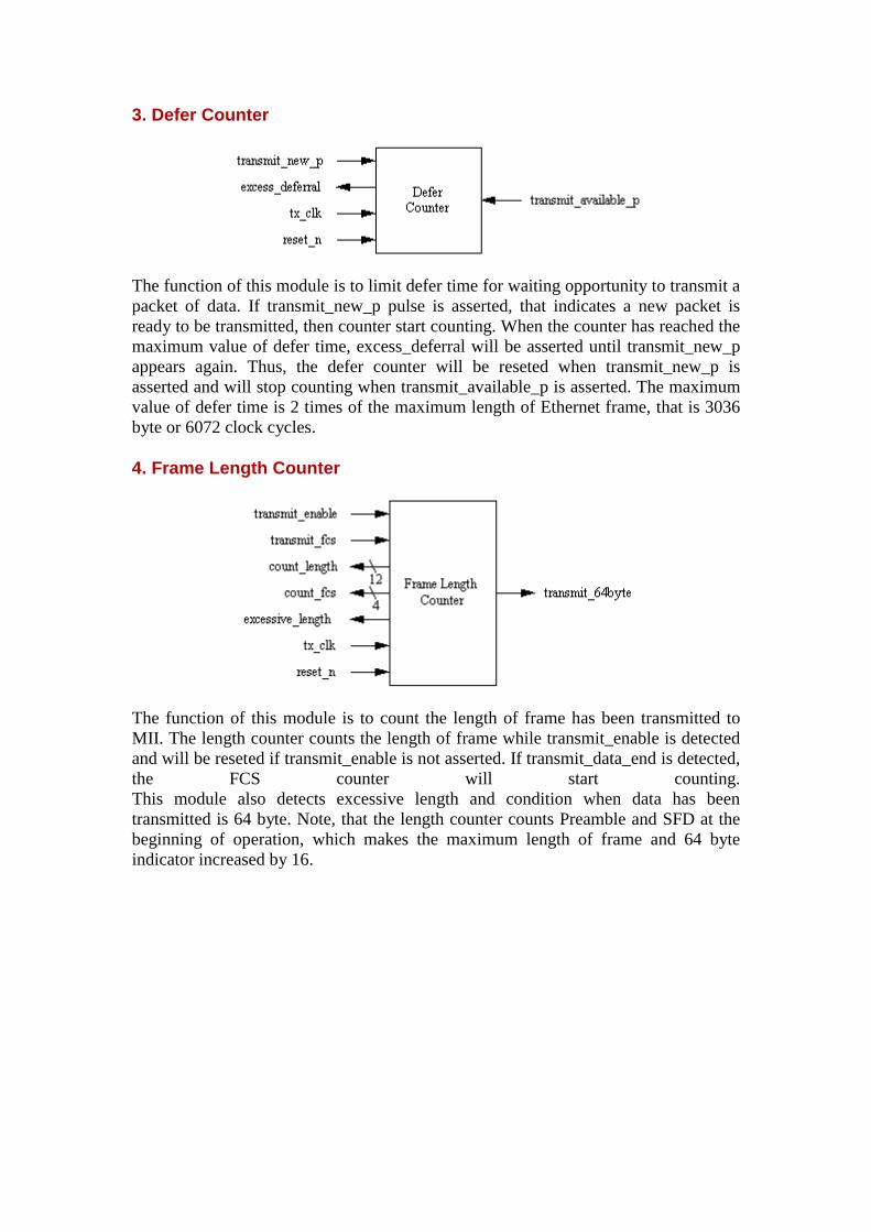
3. Defer Counter
The function of this module is to limit defer time for waiting opportunity to transmit a packet of data. If transmit_new_p pulse is asserted, that indicates a new packet is ready to be transmitted, then counter start counting. When the counter has reached the maximum value of defer time, excess_deferral will be asserted until transmit_new_p appears again. Thus, the defer counter will be reseted when transmit_new_p is asserted and will stop counting when transmit_available_p is asserted. The maximum value of defer time is 2 times of the maximum length of Ethernet frame, that is 3036 byte or 6072 clock cycles.
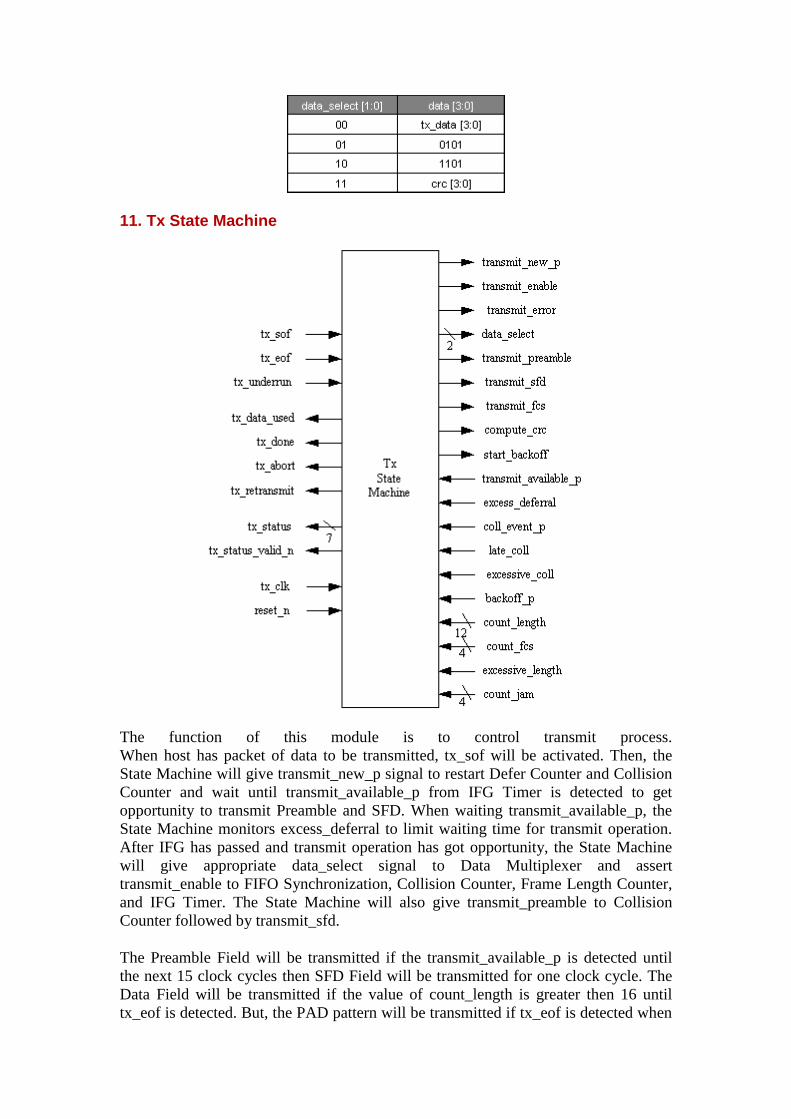
4. Frame Length Counter
The function of this module is to count the length of frame has been transmitted to MII. The length counter counts the length of frame while transmit_enable is detected and will be reseted if transmit_enable is not asserted. If transmit_data_end is detected, the FCS counter will start counting. This module also detects excessive length and condition when data has been transmitted is 64 byte. Note, that the length counter counts Preamble and SFD at the beginning of operation, which makes the maximum length of frame and 64 byte indicator increased by 16.

5. Collision Counter
The functions of this module are to count collision events, inspect number of consecutive collisions, and detect late collision. If collision appears while transmit_enable is asserted and coll_event_p is asserted. Then, the value of counter is increamented. But, if collision is detected while Tx Eth MAC transmits Preamble or SFD, coll_event_p will be activated after all Preamble and SFD patterns have been transmitted. If collision is detected when the value of counter is 15, then excessive_coll is asserted and will be deasserted when a new packet comes. If collision is detected when transmit_64byte has been asserted by Frame Length Counter, late collision occurs. When operates in full duplex mode, this module ignores any collision signals.
6. Random Number Generator
This module generates random number using Linear Feedback Shift Register which contains 10 bit register. This Random Number Generator will select random number from range between 0 to (2k)-1 with k is the smaller number between number of collision and 10. The number of collision is equal to coll_attempt.

7. Backoff Timer
The function of this module is to determine interval time for backoff operation after a start_backoff is detected. This interval time is calculated from multiplication between random number and slot time, that is random x 128 clock cycles. This module takes random number from Random Number Generator when start_backoff is detected.
8. Jam Timer
The function of this module is to determine how long JAM pattern has been transmitted after a collision.
9. CRC Generator
The function of this module is to generate CRC number, which will be added to Ethernet frame as FCS field. The CRC number is calculated from Destination Address field till Data field, includes PAD bits if exists, and will be computed while compute_crc is enabled. The Paralel CRC Algorithm is used to calculate CRC number, and CRC is calculated from 4 bits of data every one clock cycle.
10. Data Multiplexer
The function of this module is to determine which data nibbles will be transmitted to MII, which are related to data_select signal from state machine. Data nibble 4'b0101 is pattern for Preamble, JAM, and PAD. While data nibble 4'b1101 is pattern for SFD.
11. Tx State Machine
The function of this module is to control transmit process. When host has packet of data to be transmitted, tx_sof will be activated. Then, the State Machine will give transmit_new_p signal to restart Defer Counter and Collision Counter and wait until transmit_available_p from IFG Timer is detected to get opportunity to transmit Preamble and SFD. When waiting transmit_available_p, the State Machine monitors excess_deferral to limit waiting time for transmit operation. After IFG has passed and transmit operation has got opportunity, the State Machine will give appropriate data_select signal to Data Multiplexer and assert transmit_enable to FIFO Synchronization, Collision Counter, Frame Length Counter, and IFG Timer. The State Machine will also give transmit_preamble to Collision Counter followed by transmit_sfd.
The Preamble Field will be transmitted if the transmit_available_p is detected until the next 15 clock cycles then SFD Field will be transmitted for one clock cycle. The Data Field will be transmitted if the value of count_length is greater then 16 until tx_eof is detected. But, the PAD pattern will be transmitted if tx_eof is detected when
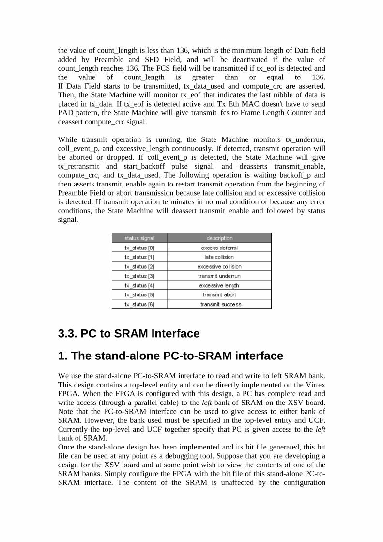
the value of count_length is less than 136, which is the minimum length of Data field added by Preamble and SFD Field, and will be deactivated if the value of count_length reaches 136. The FCS field will be transmitted if tx_eof is detected and the value of count_length is greater than or equal to 136. If Data Field starts to be transmitted, tx_data_used and compute_crc are asserted. Then, the State Machine will monitor tx_eof that indicates the last nibble of data is placed in tx_data. If tx_eof is detected active and Tx Eth MAC doesn't have to send PAD pattern, the State Machine will give transmit_fcs to Frame Length Counter and deassert compute_crc signal.
While transmit operation is running, the State Machine monitors tx_underrun, coll_event_p, and excessive_length continuously. If detected, transmit operation will be aborted or dropped. If coll_event_p is detected, the State Machine will give tx_retransmit and start_backoff pulse signal, and deasserts transmit_enable, compute_crc, and tx_data_used. The following operation is waiting backoff_p and then asserts transmit_enable again to restart transmit operation from the beginning of Preamble Field or abort transmission because late collision and or excessive collision is detected. If transmit operation terminates in normal condition or because any error conditions, the State Machine will deassert transmit_enable and followed by status signal.
3.3. PC to SRAM Interface
1. The stand-alone PC-to-SRAM interface We use the stand-alone PC-to-SRAM interface to read and write to left SRAM bank. This design contains a top-level entity and can be directly implemented on the Virtex FPGA. When the FPGA is configured with this design, a PC has complete read and write access (through a parallel cable) to the left bank of SRAM on the XSV board. Note that the PC-to-SRAM interface can be used to give access to either bank of SRAM. However, the bank used must be specified in the top-level entity and UCF. Currently the top-level and UCF together specify that PC is given access to the left bank of SRAM. Once the stand-alone design has been implemented and its bit file generated, this bit file can be used at any point as a debugging tool. Suppose that you are developing a design for the XSV board and at some point wish to view the contents of one of the SRAM banks. Simply configure the FPGA with the bit file of this stand-alone PC-to-SRAM interface. The content of the SRAM is unaffected by the configuration
process. Once the interface is programmed into the FPGA, a utility programme on the PC can be used to view (and even change) the SRAM contents. A Visual Basic programme that provides these features, "XSVSRAMUtility.exe" is included with this resource collection. List of modules :
• pctoleftsramtoplevel-sv02 This file contains the top-level entity for the design, which is called "pctosramtoplevel". This entity connects the PC-to-SRAM interface to the left bank of XSV SRAM.
• pctosraminterface-sv06.vhd This VHDL module is responsible for implementing the communication protocol that is used between the PC and the XSV board. It translates requests from the PC into signals for the SRAM interface module and vice-versa.
• sram512kleft16bit50mhzreadreq-sv05 This is an SRAM interface module, which provides the actual access to the SRAM bank. For more information on this module, see the document describing the "SRAM Interface" design.
The SRAM interface in this file uses a 2 clock cycle read.
2. The PC-to-SRAM interface VHDL module We embed this design into 10/100 Mbps Ethernet MAC for debugging and tests purposes. In addition to the stand-alone version of the PC-to-SRAM interface, there is a reusable VHDL design that provides the same functionality. List of modules embedded to 10/100 Mbps Ethernet MAC design :
• sram512kleft16bit50mhzreadreq-sv05 The PC-to-SRAM interface module internally uses the SRAM interface module in this file to provide the direct SRAM access capabilities. See section 2.0, "The stand-alone design vs. the VHDL module" above. The SRAM interface in this file uses a 2 clock cycle read. If you wish to use a 1 clock cycle read then the file "sram512kleft16bit50mhzreadreq-sv05c.vhd" can be used in place of this file.
• memorymultiplexor-sv01 The VHDL entity "memorymultiplexor" in this file multiplexes the connections to the SRAM interface module. At any point in time, the SRAM interface is either to be connected to the user design (allowing the design normal SRAM access) or to the "pctosraminterface" entity (allowing a PC access to the SRAM). This VHDL file takes care of switching these connections as necessary.

• pctosraminterface-sv06 This VHDL module is responsible for implementing the communication protocol that is used between the PC and the XSV board. It translates requests from the PC into signals for the SRAM interface module and
vice-versa. 4. Files Needed for This Design List of Files
• backoff_timer.v • coll_counter.v • crc_gen.v • data_mux.v • defer_counter.v • dff_tx.v • fifo_synch.v • frame_length_counter.v • ifg_timer.v • jam_timer.v • pctosraminterface-sv06.vhd • memorymultiplexor-sv01.vhd • random_number_gen.v • sram512kleft16bit50mhzreadreq-sv05.vhd • tx_ethmac.v • tx_state_machine.v • rx_sm.v • rx_fcs.v • rx_buffer.v • rx_mac2.v • rx_sfd.v • rx_aml.v • mac.vhd
File Descriptions backoff_timer.v determines interval time for backoff operation after a start_backoff is detected coll_counter.v counts collision events, inspects number of consecutive collisions, and detects late collision crc_gen.v generates CRC number, which will be added to Ethernet frame as FCS field

data_mux.v determines which data nibbles will be transmitted to MII, which are related to data_select signal from state machine defer_counter.v limits defer time for waiting opportunity to transmit a packet of data dff_tx.v D Flip-Flop Module with active low reset fifo_synch.v keeps synchronization all outputs with the rising edge of input clock frame_length_counter.v counts the length of frame has been transmitted to MII ifg_timer.v assures time interval between two packets of data or Inter Frame Gap (IFG) is 96 bit time or 24 clock cycles jam_timer.v determines how long JAM pattern has been transmitted after a collision pctosraminterface-sv06.vhd provides an interface to the SRAM controller that allows the PC to read and write to the SRAM via the parallel port memorymultiplexor-sv01.vhd allows either the PC or the IP stack to access RAM random_number_gen.v generates random number using Linear Feedback Shift Register which contains 10 bit register with polinomial feedback is feedback = x[2] XNOR x[9] sram512kleft16bit50mhzreadreq-sv05.v main interface to the left bank RAM, controls reading and writing tx_ethmac.v Ethernet MAC transmitter top level module tx_state_machine.v controls transmit process rx_sm.v controls all receive process rx_fcs.v checks the CRC code in FCS field

rx_buffer.v holds packet data nibble to get SFD detector ready to process the first nibble and does data decapsulation by allowing packet data go through rx buffer after the SFD detected rx_mac2.v Ethernet MAC receiver top level module rx_sfd.v detects the SFD that indicates the beginning of data to be transfer to FIFO rx_aml.v checks destination address field mac.vhd Ethernet MAC top level module 5. Implementation of 10/100 Mbps Ethernet MAC 10/100 Mbps Ethernet MAC consists of transmitter and receiver, which are combined into one design. Besides that, SRAM Interface was embedded to 10/100 Mbps Ethernet MAC design (Figure 2). In order to combine these modules, we modified the transmitter and receiver design. This is done to simplify debugging and tests purposes. Besides that, we modify the design, so it can access SRAM left bank on XSV board.
Figure 2. Implementation of 10/100 Mbps Ethernet MAC on XSV board

Modified Design
1. Ethernet MAC Transmitter
Data, which wants to be transmitted, is written into SRAM first. The transmitter sends the data stored in SRAM, not the data from external input.
2. Ethernet MAC Receiver
Ethernet address is set to a constant, not as input anymore. Data packet received and status bits is stored into SRAM. We can see the status of data receiving process by checking status bits in SRAM.
Testing Implemented 10/100 Mbps Ethernet MAC design on XSV board
1. Testing Ethernet MAC Transmitter
In order to test the transmitter design, we connect XSV board to PC Ethernet Card using UTP cross-over cable. After that, we actives the transmitter and use Network Monitor utility to see data received by PC Ethernet Card.
2. Testing Ethernet MAC Receiver
There are two methods used to test the receiver design :
• Receiving data packet from LAN • Receiving data packet from PC
Then, we check the data received and status bits stored in SRAM. Status bits show that receiving data process runs correctly.
6. Design Considerations
Design Limitations
Key limitation of this design is Ethernet MAC works on half-duplex mode. We need MII Management Module and MAC Control Module to make it works on full-duplex mode. The MAC Control Module performs a real-time flow control function for the full duplex operation. Control opcode PAUSE is used for stopping the station that is transmitting the packets. The receive buffer (FIFO) starts to fill up when the upper

layer cannot keep up accepting the incoming packets. Before an overflow happens, the upper layer sends a control frame PAUSE to the transmitting station. This control frame inhibits the transmission of the data frames for a specified period of time. When the MAC Control module receives a PAUSE control frame, it loads the pause timer with the value received in the pause timer value field. The Tx MAC is stopped (paused) from transmitting the data frames for the "pause timer value" slot times. Pause timer decrements one each time a slot time passes by. When the pause time number equals to zero, the MAC transmitter resumes the transmit operation. MII Management module is a simple two-wire interface between the host and an external PHY device. It is used for configuration and status read of the physical device. The physical interface consists of a management data line MDIO and a clock line MDC. During the read/write operation the most significant bit is shifted in/out first from/to the MDIO data signal. On each rising edge of the MDC a shift register is shifted to the left and a new value appears on the MDIO. The other limitation is the transmitter can only send a few bytes. There will be updated files for the transmitter.
Design Notes Please note that this design has been fully tested and no problems have been witnessed with it running at 25 MHz (even though Foundation reports a much lower clock speed should be the maximum for several reasons). However, synthesising and implementing with a full optimisation effort is recommended. In the reprogramming of the CPLD to set the PHY to the correct modes, several of the PHY outputs to the CPLD were also mapped to LEDs, and as such these LEDs should not be driven by anything else unless the CPLD vhd file is changed, the svf file is rewritten and then the CPLD is reprogrammed with the new svf. The list of remapped LEDs are: LEDS (Speed LED) – LED 5 of the right hex display – active low indicates 100Mb/s operation LEDL (Link LED) – LED 6 of the right hex display – active low indicates a valid link LEDR (Receive LED) – Bar(0) – active low indicates a frame is being received LEDT (Transmit LED) – Bar(1) – active low indicates a frame is being transmitted These are all feed through nets. Check cpldnet.vhd for more information on these connections. 7. Memory Map
The Ethernet MAC only uses the left bank of memory to hold the data used by the transmitter and to store data received by the receiver. Below is a memory map of what portions of the RAM are used and what parts are free. The free parts of the memory are available to hold more buffers.
Memory Range (hex) Memory Usage
00000 - 0FFFF Transmitter buffer - holds data to be sent by the transmitter

10000 - 1FFFF Free 20000 - 1FFFF Free
30000 - 1FFFF Receiver buffer - stores data received by the receiver
40000 - 1FFFF Free 50000 - 1FFFF Free
60000 - 1FFFF Status buffer - stores status bits produced by the receiver
70000 - 1FFFF Free