XPS Applications in Thin Films Research · XPS Applications in Thin Films Research Shujiang Geng 1,...
16
XPS Applications in Thin Films Research Shujiang Geng 1 , Sam Zhang 1 and H. Onishi 2 1. School of Mechanical & Production Engineering, Nanyang Technological University, 50 Nanyang Avenue 639798 Singapore 2. Shimadzu (Asia Pacific) Pte Ltd, 16 Science Park Drive, Singapore 118227 Abstract: XPS (X-ray Photoelectron Spectroscopy) or ESCA (Electron Spectroscopy for Chemical Analysis) as a surface analytical technique has been developed over years and has been used successfully in characterization of a variety of thin films. Information such as composition, chemical states, depth profile, imaging and thickness of thin films is especially useful in thin film research. This paper aims at reviewing these applications of XPS in thin film area. Keywords: XPS, ESCA, applications, thin films Introduction XPS (X-ray Photoelectron Spectroscopy) or ESCA (Electron Spectroscopy for Chemical Analysis) as a surface analysis technique has been most widely used due to its high information content, flexibility in addressing a wide variety of samples and sound theoretical basis since K. Siegbahn and his research group developed the instrumentation and theory of it in the mid 1960s 1 . Over the past few decades XPS has been developed into the key surface characterization method which combines surface sensitivity with the ability to quantitatively obtain both elemental and chemical state information 2 . Data interpretation has been established within a number of published databases 3, 4 and in the modern times on-line services have become available on the World Wide Web 5 . As we know, nowadays XPS is a very important analytical tool in the area of thin films 6 . XPS analysis gives rise to useful information such as composition, chemical state, and thickness etc. of thin films. This paper reviewed these applications with emphasis on thin film composition, imaging and thickness measurements.
Transcript of XPS Applications in Thin Films Research · XPS Applications in Thin Films Research Shujiang Geng 1,...

XPS Applications in Thin Films Research
Shujiang Geng 1, Sam Zhang 1 and H. Onishi 2
1. School of Mechanical & Production Engineering, Nanyang Technological University, 50
Nanyang Avenue 639798 Singapore
2. Shimadzu (Asia Pacific) Pte Ltd, 16 Science Park Drive, Singapore 118227
Abstract: XPS (X-ray Photoelectron Spectroscopy) or ESCA (Electron Spectroscopy for
Chemical Analysis) as a surface analytical technique has been developed over years and has been
used successfully in characterization of a variety of thin films. Information such as composition,
chemical states, depth profile, imaging and thickness of thin films is especially useful in thin film
research. This paper aims at reviewing these applications of XPS in thin film area.
Keywords: XPS, ESCA, applications, thin films
Introduction
XPS (X-ray Photoelectron Spectroscopy) or ESCA (Electron Spectroscopy for Chemical
Analysis) as a surface analysis technique has been most widely used due to its high information
content, flexibility in addressing a wide variety of samples and sound theoretical basis since K.
Siegbahn and his research group developed the instrumentation and theory of it in the mid 1960s 1. Over the past few decades XPS has been developed into the key surface characterization
method which combines surface sensitivity with the ability to quantitatively obtain both
elemental and chemical state information 2. Data interpretation has been established within a
number of published databases 3, 4 and in the modern times on-line services have become
available on the World Wide Web 5. As we know, nowadays XPS is a very important analytical
tool in the area of thin films 6. XPS analysis gives rise to useful information such as composition,
chemical state, and thickness etc. of thin films. This paper reviewed these applications with
emphasis on thin film composition, imaging and thickness measurements.

1. Composition and Chemical state
The principle of XPS is based on the photoelectric effect outlined by Einstein in 1905 where
the concept of the photon was used to describe the ejection of electrons from a surface when
photons impinge upon it. This process can be expressed by the following equation 1:
BE = νh − KE − φ (1)
Where BE is the binding energy of the electron in the atom (a function of the type of atom and its
environment), νh is the photon energy of X-ray source, KE is the kinetic energy of the emitted
electron that is measured in the XPS spectrometer and φ is the spectrometer work function. For
XPS, Al Kα (1486.6eV) or Mg Kα (1253.6eV) is often the photon energies of choice. Other X-
ray lines can also be chosen such as Ti Kα (2040eV). The XPS technique is highly surface
specific due to the short range of the photoelectrons that are excited from the solid. The energy
of the photoelectrons leaving the sample is determined using an analyzer and this gives a
spectrum with a series of photoelectron peaks. The binding energy of the peaks are characteristic
of each element. The peak areas can be used (with appropriate sensitivity factors) to determine
the composition of the materials surface. The shape of each peak and the binding energy can be
slightly altered by the chemical state of the emitting atom. Hence XPS can provide chemical
bonding information as well. XPS is not sensitive to hydrogen or helium, but can detect all other
elements. Normally, in the outmost 10nm of thin films surface XPS can identify all elements
(present at concentration >0.1 atomic %) except H and He 1. The analysis of composition has
been widely applied in the thin film research fields. We can obtain the composition of thin films
from XPS spectra. The information of all elements in thin film can be gained from the survey
scan spectrum of XPS. The detailed information of each element in the thin film can be obtained
from the narrow scan spectrum of XPS.
1.1 Survey scan spectra of thin films
The information of elements in thin films and contamination adsorbed on the thin films can be
given from the wide scan spectra of XPS. Fig. 1 shows the survey spectra (pass energy of 160eV
was applied) for typical undoped and doped TiO2 films on silicon wafer 7. C KLL, Ti LMM and
O KLL Auger peaks and XPS spectra peaks of Ti, O and C were recorded for both the undoped
and doped TiO2 film. The peaks of Nb3d and Nb3p detected from the doped TiO2 film were very
weak (See Fig.1 b).
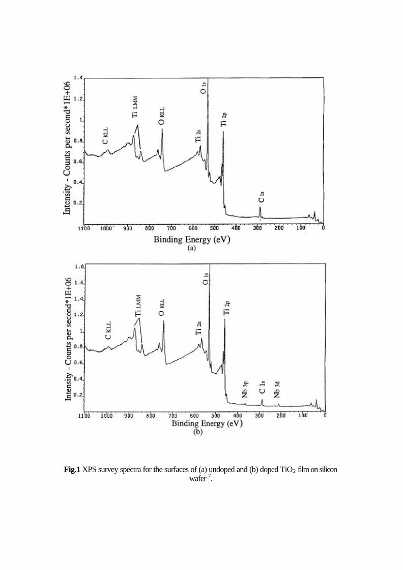
Fig.1 XPS survey spectra for the surfaces of (a) undoped and (b) doped TiO2 film on silicon wafer 7.

1.2 Narrow scan spectra of thin films
Narrow scan gives detailed information of each element in thin films. Fig.2 through Fig.5
show the narrow scan spectra (pass energy of 20 eV was used) of C1s, Ti2p, O1s and Nb3d for
both undoped and doped films 7. The chemical composition of both film surfaces can be
calculated from these spectra. The calculation is based on the integrated area under the assigned
element peak and the sensitivity factor for the element 8. Furthermore, Fig.3 and Fig.5 indicated
that the peak position of Ti2p3/2 corresponds to that of the Ti4+ oxidation state and the center of
the Nb3d3/2 peak corresponds to that of Nb5+ oxidation state. One point should be noted, the
spectra must be calibrated with the standard sample such as Au 4f7/2 and Ag 3d5/2. For AXIS
Ultra type XPS apparatus, the bending energy of Au 4f7/2 is 83.89 eV (Al Kα ) or 84.00 eV (Mg
Kα ) and that of Ag 3d5/2 is 368.26 eV (Al Kα ) or 368.27 eV (Mg Kα ). Normally, the simple
calibration is done by C1s (approximately 285 eV) spectrum of adventitious carbon that exists on
all samples.
Fig.2 C1s spectra: (a) doped and (b) undoped films 7
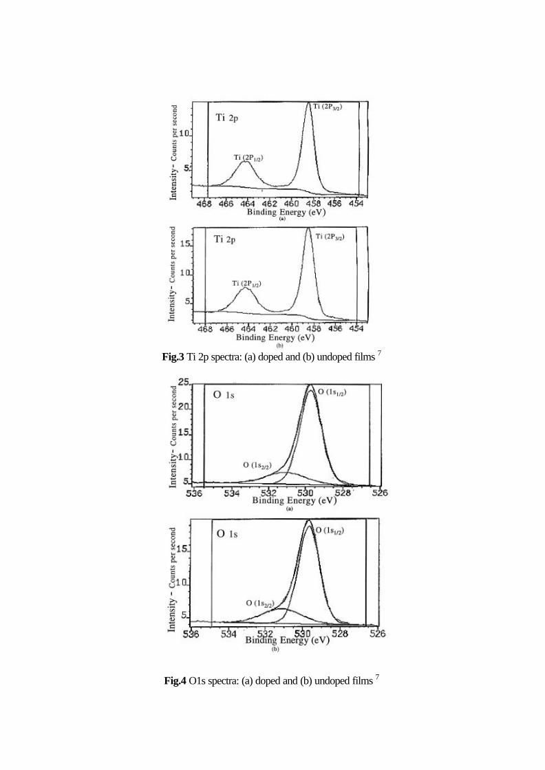
Fig.3 Ti 2p spectra: (a) doped and (b) undoped films 7
Fig.4 O1s spectra: (a) doped and (b) undoped films 7

Fig.5 Nb3d spectra for doped films 7
It is very important to deconvolute these spectra in thin film elemental analysis. Extra care
must be exercised in deconvoluting a spectrum since quite a degree of human judgement is
involved the process. For example, the XPS spectra of O1s in Fig.4 show a two-band structure.
The dominant peak at 529.7 eV is characteristic of metallic oxides, which is in agreement with
O1s electron binding energy for TiO2 and also is assigned to the niobium for doped samples 9.
Another O1s band at 531.1 eV may be attributed to different oxidized hydrocarbon
(contamination).
2. Depth analysis
In XPS, two methods can be used for composition variation with depth of thin film, the non-
destructive analysis and the destructive analysis.
2.1 Non-destructive depth profiling
The escape depth of a photoelectron increases with its kinetic energy in the energy range
higher than 50 eV. One of the non-destructive analysis is analyzing XPS spectra at varying
photoelectron take-off angles 10, 11. Another method is using a high-energy and continuously
variable-energy source in order to observe the dependence of the signal intensity on the kinetic
energy of the photoelectron and therefore on the electron escape depth at a given take-off angle 12.

Fig.6 shows that varying the collection angleθ will change the sensitivity to the surface 13. At
very low take-off angles (90º−θ ), most of the collected electrons originate from atoms near the
surface, but at higher take-off angles more electrons will be collected from atoms deeper in the
sample.
Fig.6 Schematic drawing showing the variation of sampling depth as a function of take-off angle in X-ray photoemission experiments. (a) At normal incidence (θ = 0º), the escape depth is equal to the attenuation length λ . This geometry probes the deepest into the sample. (b) At shallow take-off angles (large θ), the escape depth (which equals λcosθ) is less than the attenuation
length, and only photoelectrons close to the surface (within a distance λ cosθ from the surface) are detected. Thus, photoelectrons from atom in plane 2 and below have to travel a distance greater
than the attenuation length and are less likely to be detected, unlike those from plane 1 and above13.
Fig.7 gives an example of how the photoemission features corresponding to the near surface
region of a thin silicon dioxide film on silicon are enhanced relative to the bulk Si signal on
going to low (i.e., shallow) take-off angles 13. A comparison of region A and B for spectra
recorded at 25º and 75º clearly shows an increase in the relative intensity of the oxidized Si
features at the lower take-off angle.
Thus, if one is interested in characterizing the surface layer of thin films, one should perform
photoemission measurement at low take-off angles to emphasize the surface layer features.
However, the depth resolution of this method deteriorates with decreasing take-off angle.
Furthermore, surface roughness and contamination of the specimen also affect the depth
resolution.

Fig.7 X-ray photoemission spectra of the Si 2p region, recorded at different take-off angles 13
Another method of non-destructive analysis for deeper surface region is the use of a high-
energy and continuously variable-energy source, such as synchrotron radiation (SR) 12. In this
case, relative intensities measured at a given take-off angle are essentially independent of the
surface toughness. Fig.8 shows the photon energy dependence of the Si 1s XPS spectra for the
Si(100) oxidized at 700°C for 30min. Peaks A and B can be assigned as elemental Si and SiO2,
respectively. The relative intensity of peak A increases gradually with the photon energy, in
contrast with peak B. This result indicates that the Si substrate is being observed since the depth
of photoelectrons becomes larger with an increasing kinetic energy.

Fig.8 Si 1s XPS spectra for the oxidized Si (700°C, 30min), taken at various photon energies. The spectra were obtained at increments of about 200 eV between 2001.7 eV and 5380.7 eV.
The photon energies used for each spectrum are shown on the right-hand axis 12.
2.2 Destructive depth profiling
The destructive depth profiling is realized by bombardment of the film surface with Ar+ ions
at controlled power and timing. After certain time of this “bombardment erosion”, the
composition is analyzed before next bombardment starts. Thus a composition depth profile is
obtained. Fig.9 shows the XPS depth profile of Ti0.4Al0.6N thin film annealed at 700°C for
10min in pure oxygen 14.
Fig.9 XPS depth profile of Ti0.4Al0.6N thin film on Si substrate 14

3. Imaging
In 1995, the first chemical XPS images of thin film grain boundaries was acquired 15. The
elemental distribution of thin films can be revealed by XPS imaging. Fig.10 is an example of the
best resolution IXPS currently available (with a spatial resolution up to 10nm) 6. A thin silicon
nitrate film was grown on a silicon wafer. Composition imaging provides a valuable way to
examine the compositional uniformity or segregation of elements in thin films. Fig.11 shows the
lateral distribution of a laser ablated hole on the poly sample (20 pulses with 0.55J/cm2; ø =
300µm) of carbon (C1s) and oxygen (O1s) recorded with XPS imaging 16. The concentration of
C is lower within the hole than that outside the hole, while the O1s concentration within the hole
is higher than that outside the hole.
Fig.10 XPS images. (a) The N1s and (b) the O1s signal distribution of oxidized silicon pattern in
a silicon-nitrate matrix, (c) overlay image 6.
Fig.11 Carbon (C1s) and oxygen (O1s) distribution of a laser ablated hole measured by XPS imaging. Brighter color indicates higher concentration 16.

4. Thickness
XPS can offer precise thickness measurements for ultra thin films. The SiO2 thickness oxd was
determined using the following equation 17, 18:
oxd = oxλ sinθ ln
+ 1
Si
ox
II
β (2)
where oxλ is the attenuation length of the Si 2p photoelectrons in SiO 2, θ is a photoelectron take-
off angle, i.e. the angle between the sample surface plane and the incident beam, β = ∞oxI / ∞
SiI
(where ∞oxI and ∞
SiI are the Si2p intensities of “infinitely thick” (greater than 30nm) SiO2 and Si,
respectively) and oxI / SiI is the ratio of intensities from the unknown film. Unfortunately, there is
considerable disagreement in the XPS literature in the two sample-dependent constants: oxλ and
β . Reported oxλ values vary from 2.4-3.8nm, while β varies from 0.6-1.01 18, 19, 20, 21, 22. It has
been suggested that much of the discrepancy in the reported oxλ values stems from the use of
poorly calibrated ellipsometry ‘standards’ that tend to overestimate the thickness of ultra thin
SiO2 films 18, 23, 24, 25, 26. For this reason, it was decided to use an attenuation length of
2.7± 0.2nm, averaged from four different TEM/XPS publications 18, 19, 20. The value of β was
determined by analyzing two different standard samples: a 5%HF etched Si (100) surface and a
thick thermal SiO2 film which is thicker than 30nm. Both standards were lightly sputtered with 3
keV Ar+ to remove absorbed organic species and the native oxide and fluoride (on the HF etched
Si sample). Normally, the β value is about between 0.75 and 0.85 20, 27.
For ultra-thin films, XPS gives very precise thickness. Fig.12 shows the ability of XPS to
measure very small difference in ultra-thin oxides of SiO2 27. Although TEM can offer the
precise thickness measurement, analysis on films thinner than 1nm is extremely difficult 28.
Furthermore TEM sample preparation is also an arduous endeavor. In order to check the
precision of thickness measurement by XPS, the same sample of SiO2 film was measured by
both XPS and TEM. According to Fig. 13 20 and Eq (2), the calculated thickness of SiO2 film is
6.4nm which is amazingly the same as the TEM result (Fig.14) 20. XPS is so sensitive to small
changes in oxide thickness for ultra-thin films (<2nm, the precision is ± 0.1nm). However, the
inherent limitation is its insensitivity in change in oxide thickness of thicker films (>10nm)
because the Si relative intensity decays exponentially with the increase of oxide thickness ( SiI ∝
θλ sin/de− ). This can be seen from Fig.15 27.

Fig.12 Si 2p spectra of ultra-thin SiO2 oxides showing difference of as small as 0.1nm 27
Fig.13 XPS Si 2p spectrum of a 6.4 nm SiO2 film on Si (bulk) (100) 20

Fig.14 TEM micrograph showing the thickness of SiO 2 film on Si(100) 20
Fig.15 Exponential decay of Si relative intensity of samples 27
Mitsutoshi Hoshino 29 measured the thickness of lubricant layer on magnetic recording disks
by using the XPS O1s signal ratio of lubricant and silicon dioxide according to this equation:
d = 16ln[7.2( 1I / 2I ) + 1] (3)
Where d is the thickness of lubricant layer, 1I / 2I is the ratio of the intensities of O1s
photoelectrons coming from lubricant layer (perfluoropolyether) and from silicon dioxide. It is
obvious that the thickness of lubricant layer can be calculated from the ratio of 1I / 2I that can be
obtained from the XPS spectra as demonstrated in Fig.16 for different concentration polyether.
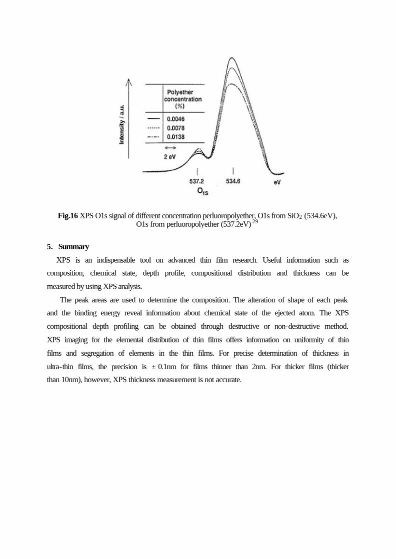
Fig.16 XPS O1s signal of different concentration perluoropolyether, O1s from SiO2 (534.6eV), O1s from perluoropolyether (537.2eV) 29
5. Summary
XPS is an indispensable tool on advanced thin film research. Useful information such as
composition, chemical state, depth profile, compositional distribution and thickness can be
measured by using XPS analysis.
The peak areas are used to determine the composition. The alteration of shape of each peak
and the binding energy reveal information about chemical state of the ejected atom. The XPS
compositional depth profiling can be obtained through destructive or non-destructive method.
XPS imaging for the elemental distribution of thin films offers information on uniformity of thin
films and segregation of elements in the thin films. For precise determination of thickness in
ultra-thin films, the precision is ± 0.1nm for films thinner than 2nm. For thicker films (thicker
than 10nm), however, XPS thickness measurement is not accurate.

References
1. John C. Vickerman: Surface Analysis-The Principal Techniques. John Wiley & Sons, 1997. 2. Briggs (Ed): Surface and Interface Analysis. 1996, 24:issue 9. 3. G Beamson, D Briggs: High Resolution XPS of Organic Polymers. John Wiley & Sons; 1992. 4. J Chastain (Ed): Handbook of X-Ray Photoelectron Spectroscopy. Minmesota: Perkin-Elmer Corporation; 1992. 5. XPS Spectral Data-Base Systems & Libraries on World Wide Web URL: http//www.xpsdata.com 6 A.J. Hartmann, R.N. Lamb X-ray photoemission spectroscopy of thin films. Current Opinion in Solid State & Materials Science 1997, 2(5): 511-516. 7 M. Z. Atashbar, H. T. Sun, B.Gong Wlodarski W., Lamb R. XPS study of Nb-doped oxygen sensing TiO2 thin films prepared by sol-gel method. Thin Solid Film 1998, 326: 238-244. 8 J. F. Moulder, W. F. Stickle, P. E. Sool, K. D. Bomben, Handbook of X-ray photoelectron spectroscopy, Perkin-Elmer, Eden Prairite, 1992. 9 C. D. Wagner, L. H. Gale, R. H. Raymond, Anal. Chem. 1979, 51(4): 466. 10 M. F. Hochella, Jr, and A. H. Carim, Surf. Sci. 1988, 197: L260. 11 M. Pijolat and G. Hollinger, Surf. Sci. 1981, 105: 114. 12 Hiroyuki Yamamoto, Yuji Baba and Teikichi A. Sasaki, Surf. Sci. 1996, 349: L133-L137. 13 Robert L. Opila, Joseph Eng Jr, Thin films and interfaces in microelectronics: composition and chemistry as function of depth 14 Hiroshi Maiwa and Noboru Ichinose, Preparation and properties of Al1-xTixN solid solution thin films by multiple cathode sputtering. Journal of the European Ceramic Society 2001, 21: 1573-1576 15 K. R. Hallam, R. K. Wild, XPS analysis of metal grain boundary surface. Surf. Interface Anal 1995, 23: 133-136 16 B. Schnyder, J. Wambach, Th. Kunz, Ch. Hahn, R. Kötz, X-ray photoelectron spectroscopy imaging of laser ablated poly(ether imide). J. Electron. Spectrosc. Relat. Phenom. 1999, 105: 113-117. 17 D. F. Mitchell, K. B. Clark, J. A. Bardell, W. N. Leonard, G. R. Massoumi and I .V. Mitchell, Film thickness measurements of SiO2 by XPS Surface and Interface Analysis, 1994, 21: 44- 50. 18 M. F. Hochella and A. F. Carim, A reassessment of electron escape depths in silicon and thermally grown silicon dioxide thin film Surface Science, 1988, 197: L260-268. 19 F. Yano, A. Hiraoka, T. Itoga, H. Kojima, K. Kanehori and Y. Mitsui, X-ray photoelectron spectroscopy study of submonolayer native oxides on HF-treated Si surfaces, J. Vacuum Science & Technol. A, 1995, 13(6): 2671-2675 20 Z. H. Lu, J. P. McCaffrey, B. Brar, G. D. Wik, R. M. Wallace, L. C. Feldman and S. P.Tay, SiO2 film thickness metrology by X-ray photoelectron spectroscopy, Applied Physics Letters, 1997, 71(19):2764-2766. 21 J. E. Fulghum, Determination of overlayer thickness by angle-resolved XPS: a comparison of algorithms, Surface and Interface Analysis., 1993, 20: 161-173. 22 R. Flitsch and S. I. Raider, Electron mean escape depths from X-ray photoelectron spectra of thermally oxidized silicon dioxide film on silicon, J. Vacuum Science & Technol., 1975, 12: 305-308 23 N. M. Ravindra, J. Narayan, D. Fathy, J. K. Srivastava and E. A. Irene, Silicon oxidation and Si-SiO2 interface of thin oxides, J. Materials Research, 1987, 2(2): 216-221.

24 A. H. Carim and R. Sinclair, The evolution of Si/SiO2 interface roughness, J. Electrochem. Society, 1987, 134(3): 741-746. 25 A. Kalnitsky, S. P. Tay, J. P. Ellul, S. Chongsawangvirod, J. W. Andrews and E. A. Irene, Measuremants and modeling of thin silicon dioxide film on silicon, J. Electrochem. Society., 1990, 137(1): 234-238. 26 S. Y. Kin and E. A. Irene, An evaluation of errors in determining the refractive index and thickness of thin SiO2 films using a rotating analyzer ellipsometer, Rev. Sci. Instrum., 1995, 66(11): 5277-5281. 27 Jeffrey R. Shallenberger, David A. Cole, Daniel F. Downey, Scott Falk and Zhiyong Zhao, Recently advances in XPS characterization of ultra-thin oxides, http://www.eaglabs.com/offline/xpsiit1.pdf 28 J.R. Shallenberger, D.A. Cole, S.W. Novak and R.L. Moore, M.J. Edgell, S.P. Smith, etal., Oxide Thickness Determination by XPS, AES, SIMS, RBS and TEM, http://www.eaglabs.com/offline/xpsiit2.pdf 29 Mitsutoshi Hoshino and Yoshihiro Kimachi, XPS measurement of lubricant layer thickness on magnetic recording disks, Journal of Electron Spectroscopy and Related Phenomena., 1996, 81: 79-85.