Xilinx Academy 4/98 1 Xilinx Software Solutions Xilinx Academy November, 1998.

Page 1
Xilinx ML501 Demo Board Tutorial
ONTAP BOUNDARY SCAN DEMONSTRATION USING THE XILINX ML501 EVALUATION PLATFORM
Reference: At www.xilinx.com search on ML501.
The project test folder for the ML501 board demo is available at http://www.flynn.com/products/downloads/ML501_JTAG_Demo.zip .
The test project unzips to a folder, \ML501_JTAG\Tutorial Test folder. The pass-word to open the file is ML501 and the software to run the project is available at www.flynn.com.
A schematic, bill-of-materials, User’s Guide, and datasheets for parts on the ML501 evaluation board are included in the Documents subdirectory. These can also be obtained from www.xilinx.com and searching on ML501.
Getting Started
onTAP® with ProScan

onTAP Series 4000Xilinx ML501 Demo Board
-Tutorial-
Page 2
1. Determine if the board under test has been built cor rectly; if not, identify faults.2. Program Flash memory.3. Configure the programmable devices.
OBJECTIVES: This document demonstrates how tests can be developed and applied within onTAP to achieve the following common bound-ary-scan related goals.
The Xilinx ML501 Evaluation Platform board provides an opportunity to dem-onstrate the following onTAP boundary-scan test and programming capabili-ties:
Test development environment for creating automated, • netlist-based inter-connect tests while managing signal transparency for components such as resistor packs.
Detection and pin-level diagnostic messages for opens, • shorts, stuck-at, bus-wire, and pull-up/down faults.
Cluster testing pipelined SRAMs, DDR2 SDRAM SODIMM • modules, LCD display, LEDs, switches.
Programming and verifying Flash memory.• Configuring FPGAs via JTAG• The ProScan program, vector, and circuit views, and a debug •
environment featuring pin wiggling, breakpoints, circuit browsing, edit settings, and single-stepping through test program instructions.
onTAP features not covered in this application include:
• Netlist merging in which netlists from multiple assemblies are combined into one project netlist.• Capacitive coupling tests.• Bus management where signal traffic is directed through bus buffers and transceivers while direction and control signals are dynamically managed.
• User-Defined Tests

onTAP Series 4000Xilinx ML501 Demo Board
-Tutorial-
Page 3
CONTENTS
onTAP Boundary Scan Demonstration Using the Xilinx ML501 Evaluation Platform..............................................1
Objectives...............................................................................................................................................................2
Introduction............................................................................................................................................................4
Creating a ‘Safe’ mode Interconnect Test on the Development screen..................................................................5
Running the Safe-Mode Interconnect Test.................................................................................................17
the Proscan screen.....................................................................................................................................19
The Test Screen..........................................................................................................................................24
Netlist Browser Screen...............................................................................................................................25
Completing the Interconnect Test........................................................................................................................26
Test and Debug...........................................................................................................................................28
Adding Cluster Tests…an SRAM Example..............................................................................................................29
Test Development for SRAM U19...............................................................................................................29
The Manufacturing Test Screen............................................................................................................................36
Summarizing Test Results......................................................................................................................................37
The SRAM DTS File................................................................................................................................................39
onTAP Series 4000Xilinx ML501 Demo Board
-Tutorial-
Page 4
INTRODUCTION: This document shows how to develop, debug, and run tests using onTAP boundary scan tools and the Xilinx ML501 Evaluation board.
A safe interconnect test is developed first, followed by an interconnect test that includes pull-up and pull-down resistor tests which expands test coverage as interacting devices are identified, brought under control, and marked ‘safe’. Cluster tests are added to test SRAM, DDR2 SODIMM memory, program and verify an Intel Strataflash, program an LCD device, test free-running clocks, LEDs and switches.
All switches on the two DIP switches should be set to the OFF position.
Before getting started, the path to a viewer for use within onTAP should be specified. This can be done from the onTAP menu, at menu item Viewer / Editor / Viewer Program. The TextPad editor (www.textpad.com) is recommended.
The tests that are developed in this tutorial may be run on onTAP’s run-rime screens including the Test screen, Mfg Test Screen, the ProScan screen, and the Net Browser screen. Also, a suite of completed tests is available in the down-
loaded project folder.
onTAP Series 4000Xilinx ML501 Demo Board
-Tutorial-
Page 6
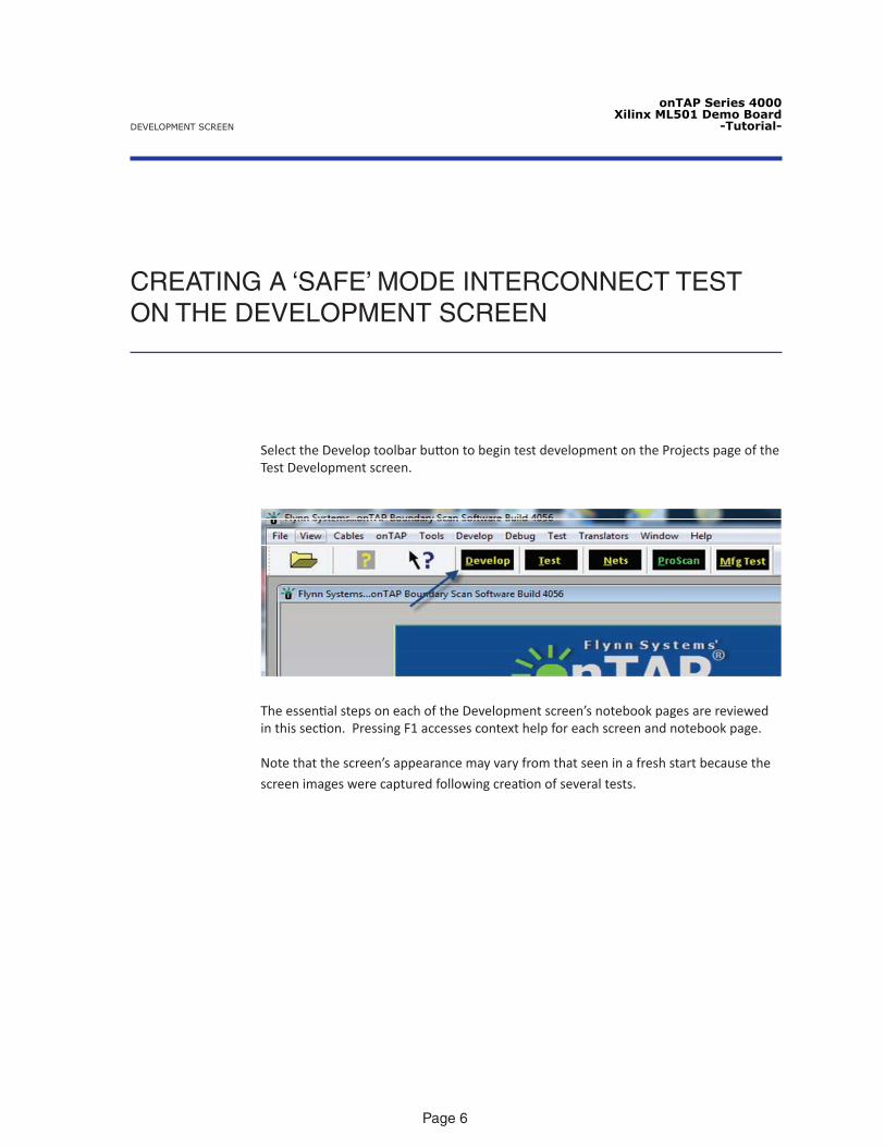
Select the Develop toolbar button to begin test development on the Projects page of the Test Development screen.
CREATING A ‘SAFE’ MODE INTERCONNECT TEST ON THE DEVELOPMENT SCREEN
The essential steps on each of the Development screen’s notebook pages are reviewed in this section. Pressing F1 accesses context help for each screen and notebook page.
Note that the screen’s appearance may vary from that seen in a fresh start because the
screen images were captured following creation of several tests.
DEVELOPMENT SCREEN
onTAP Series 4000Xilinx ML501 Demo Board
-Tutorial-
Page 7
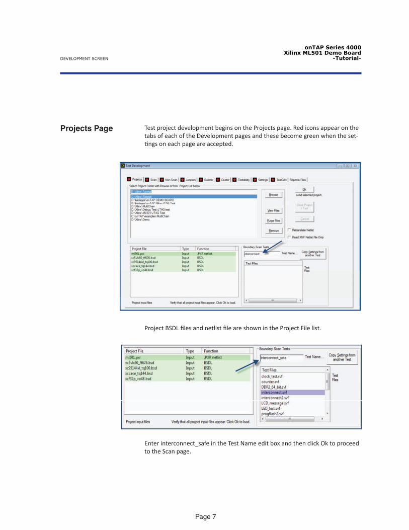
Projects Page
Enter interconnect_safe in the Test Name edit box and then click Ok to proceed to the Scan page.
Test project development begins on the Projects page. Red icons appear on the tabs of each of the Development pages and these become green when the set-tings on each page are accepted.
Project BSDL files and netlist file are shown in the Project File list.
DEVELOPMENT SCREEN
onTAP Series 4000Xilinx ML501 Demo Board
-Tutorial-
Page 8
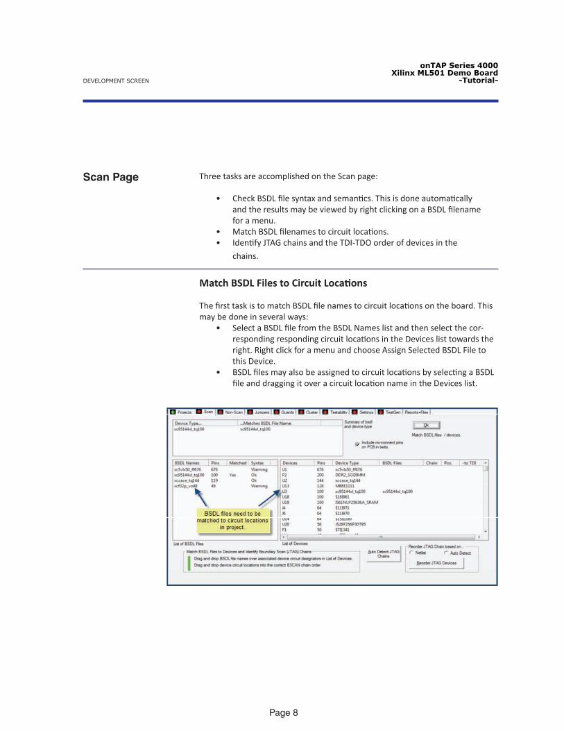
Three tasks are accomplished on the Scan page:
• Check BSDL file syntax and semantics. This is done automatically and the results may be viewed by right clicking on a BSDL filename for a menu.• Match BSDL filenames to circuit locations.• Identify JTAG chains and the TDI-TDO order of devices in the
chains.
Scan Page
Match BSDL Files to Circuit Locations
The first task is to match BSDL file names to circuit locations on the board. This may be done in several ways:
• Select a BSDL file from the BSDL Names list and then select the cor- responding responding circuit locations in the Devices list towards the right. Right click for a menu and choose Assign Selected BSDL File to this Device. • BSDL files may also be assigned to circuit locations by selecting a BSDL file and dragging it over a circuit location name in the Devices list.
DEVELOPMENT SCREEN
onTAP Series 4000Xilinx ML501 Demo Board
-Tutorial-
Page 9
Scan Page (continued)
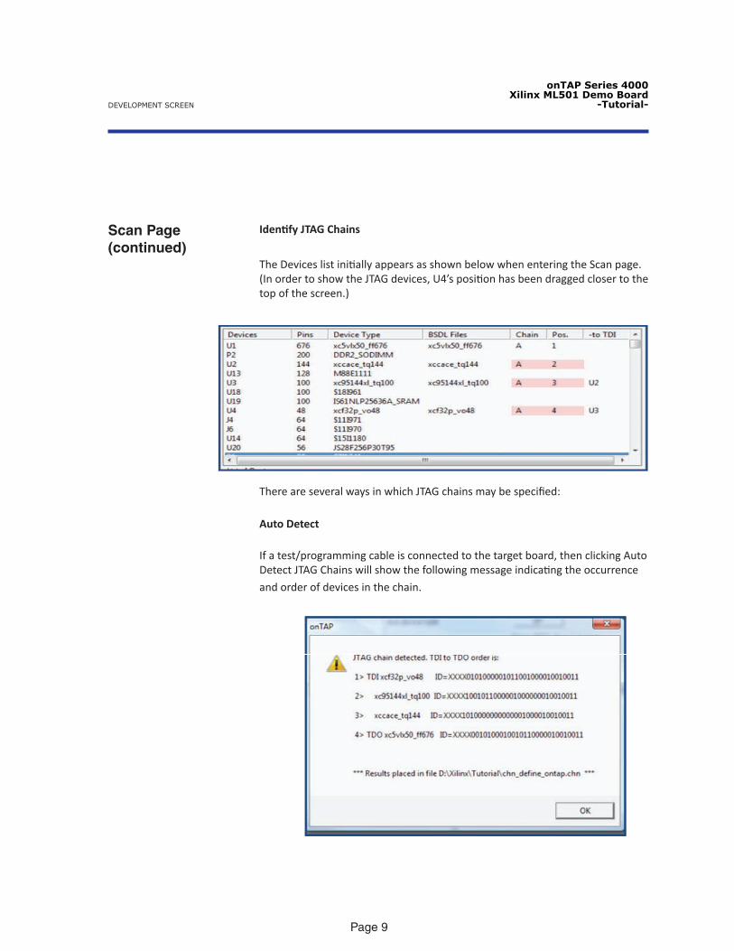
Identify JTAG Chains
The Devices list initially appears as shown below when entering the Scan page. (In order to show the JTAG devices, U4’s position has been dragged closer to the top of the screen.)
There are several ways in which JTAG chains may be specified:
If a test/programming cable is connected to the target board, then clicking Auto Detect JTAG Chains will show the following message indicating the occurrence
and order of devices in the chain.
Auto Detect
DEVELOPMENT SCREEN
onTAP Series 4000Xilinx ML501 Demo Board
-Tutorial-
Page 10
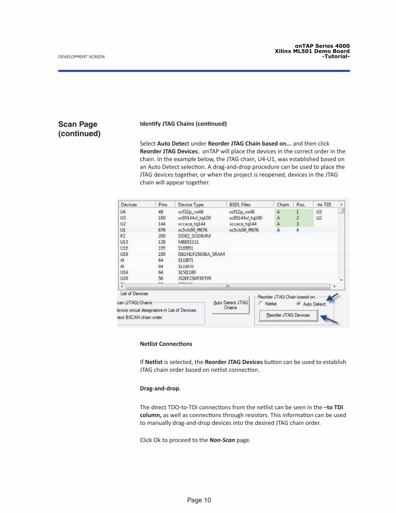
Select Auto Detect under Reorder JTAG Chain based on... and then click Reorder JTAG Devices; onTAP will place the devices in the correct order in the chain. In the example below, the JTAG chain, U4-U1, was established based on an Auto Detect selection. A drag-and-drop procedure can be used to place the JTAG devices together, or when the project is reopened, devices in the JTAG chain will appear together.
Scan Page (continued)
Identify JTAG Chains (continued)
Netlist Connections
If Netlist is selected, the Reorder JTAG Devices button can be used to establish JTAG chain order based on netlist connection.
The direct TDO-to-TDI connections from the netlist can be seen in the –to TDI column, as well as connections through resistors. This information can be used to manually drag-and-drop devices into the desired JTAG chain order.
Click Ok to proceed to the Non-Scan page.
Drag-and-drop.
DEVELOPMENT SCREEN
onTAP Series 4000Xilinx ML501 Demo Board
-Tutorial-
Page 11
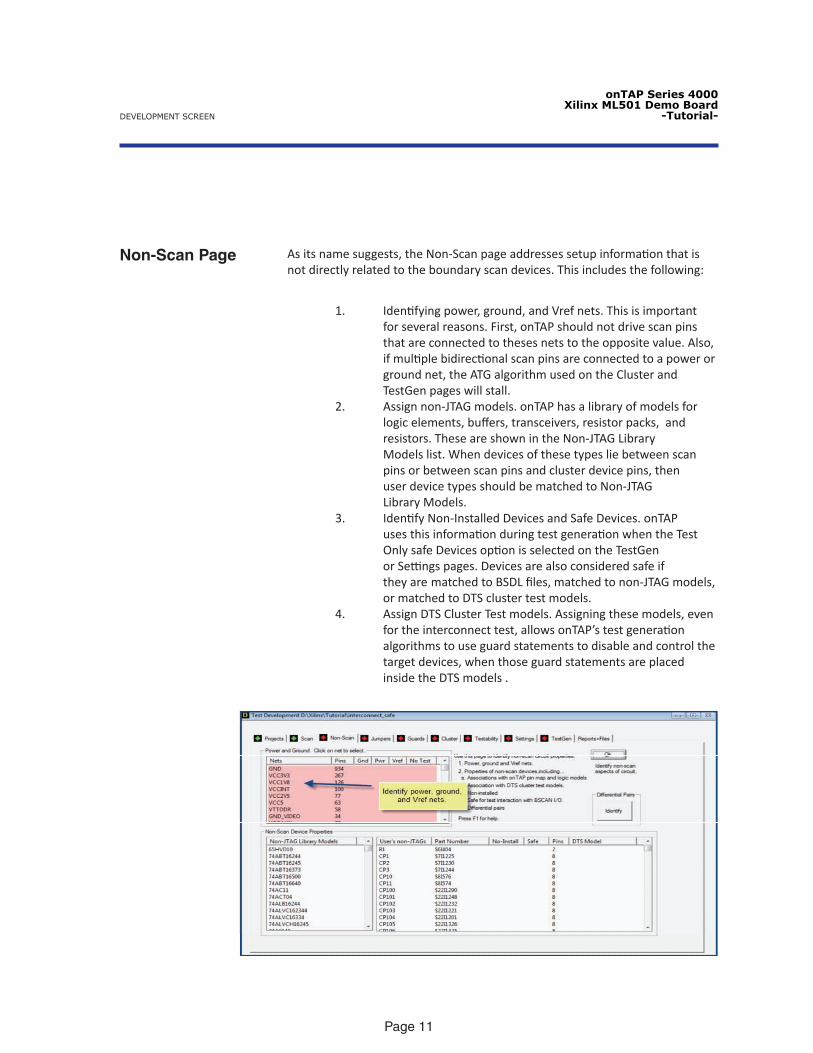
Non-Scan Page As its name suggests, the Non-Scan page addresses setup information that is not directly related to the boundary scan devices. This includes the following:
1. Identifying power, ground, and Vref nets. This is important for several reasons. First, onTAP should not drive scan pins that are connected to theses nets to the opposite value. Also, if multiple bidirectional scan pins are connected to a power or ground net, the ATG algorithm used on the Cluster and TestGen pages will stall.2. Assign non-JTAG models. onTAP has a library of models for logic elements, buffers, transceivers, resistor packs, and resistors. These are shown in the Non-JTAG Library Models list. When devices of these types lie between scan pins or between scan pins and cluster device pins, then user device types should be matched to Non-JTAG Library Models. 3. Identify Non-Installed Devices and Safe Devices. onTAP uses this information during test generation when the Test Only safe Devices option is selected on the TestGen or Settings pages. Devices are also considered safe if they are matched to BSDL files, matched to non-JTAG models, or matched to DTS cluster test models.4. Assign DTS Cluster Test models. Assigning these models, even for the interconnect test, allows onTAP’s test generation algorithms to use guard statements to disable and control the target devices, when those guard statements are placed inside the DTS models .
DEVELOPMENT SCREEN
onTAP Series 4000Xilinx ML501 Demo Board
-Tutorial-
Page 12
Non-Scan Page (continued)
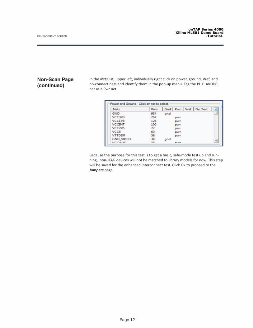
In the Nets list, upper left, individually right click on power, ground, Vref, and no-connect nets and identify them in the pop-up menu. Tag the PHY_AVDD0 net as a Pwr net.
Because the purpose for this test is to get a basic, safe-mode test up and run-ning, non-JTAG devices will not be matched to library models for now. This step will be saved for the enhanced interconnect test. Click Ok to proceed to the Jumpers page.
DEVELOPMENT SCREEN
onTAP Series 4000Xilinx ML501 Demo Board
-Tutorial-
Page 13
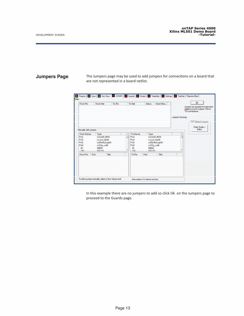
Jumpers Page The Jumpers page may be used to add jumpers for connections on a board that are not represented in a board netlist.
In this example there are no jumpers to add so click Ok on the Jumpers page to proceed to the Guards page.
DEVELOPMENT SCREEN
onTAP Series 4000Xilinx ML501 Demo Board
-Tutorial-
Page 14
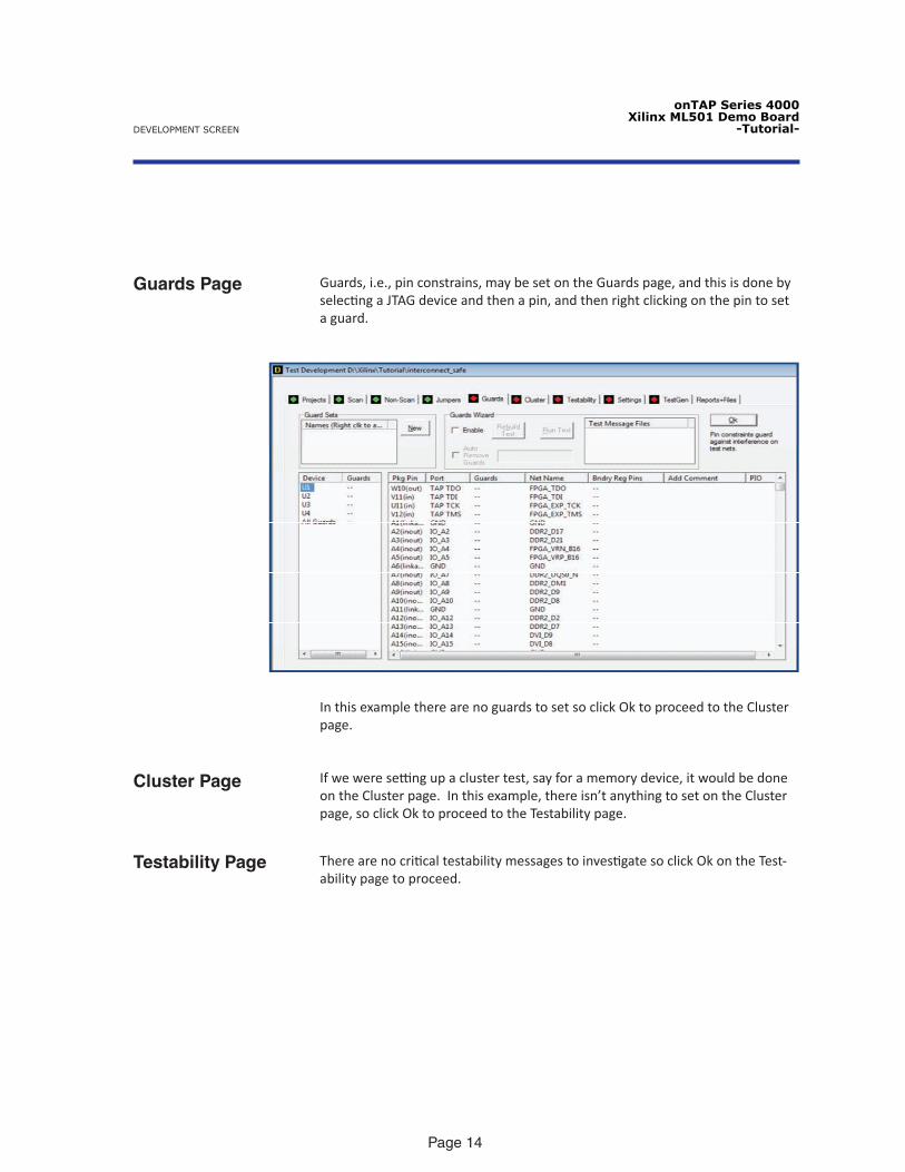
Guards Page Guards, i.e., pin constrains, may be set on the Guards page, and this is done by selecting a JTAG device and then a pin, and then right clicking on the pin to set a guard.
In this example there are no guards to set so click Ok to proceed to the Cluster page.
Cluster Page If we were setting up a cluster test, say for a memory device, it would be done on the Cluster page. In this example, there isn’t anything to set on the Cluster page, so click Ok to proceed to the Testability page.
Testability Page There are no critical testability messages to investigate so click Ok on the Test-ability page to proceed.
DEVELOPMENT SCREEN
onTAP Series 4000Xilinx ML501 Demo Board
-Tutorial-
Page 15
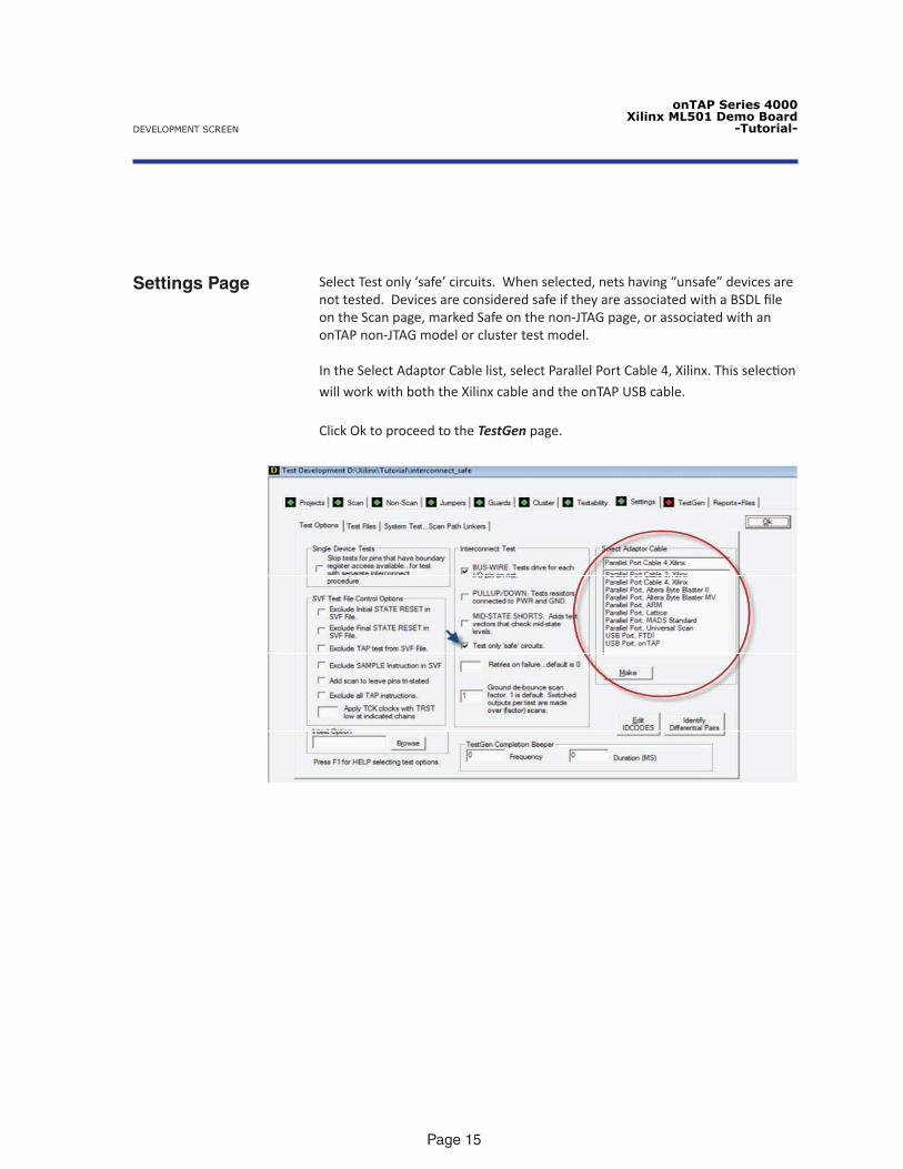
Settings Page Select Test only ‘safe’ circuits. When selected, nets having “unsafe” devices are not tested. Devices are considered safe if they are associated with a BSDL file on the Scan page, marked Safe on the non-JTAG page, or associated with an onTAP non-JTAG model or cluster test model.
In the Select Adaptor Cable list, select Parallel Port Cable 4, Xilinx. This selection
will work with both the Xilinx cable and the onTAP USB cable.
Click Ok to proceed to the TestGen page.
DEVELOPMENT SCREEN
onTAP Series 4000Xilinx ML501 Demo Board
-Tutorial-
Page 16
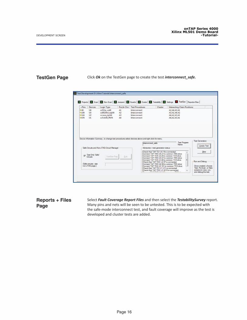
TestGen Page Click Ok on the TestGen page to create the test interconnect_safe.
Reports + Files Page
Select Fault Coverage Report Files and then select the TestabilitySurvey report. Many pins and nets will be seen to be untested. This is to be expected with the safe-mode interconnect test, and fault coverage will improve as the test is developed and cluster tests are added.
DEVELOPMENT SCREEN
onTAP Series 4000Xilinx ML501 Demo Board
-Tutorial-
Page 17
RUNNING THE SAFE-MODE INTERCONNECT TEST
The interconnect_safe.svf file can be run directly on any one of the test screens, but we will use the ProScan screen which offers many graphical debug tools to check initial results and begin the debug process.
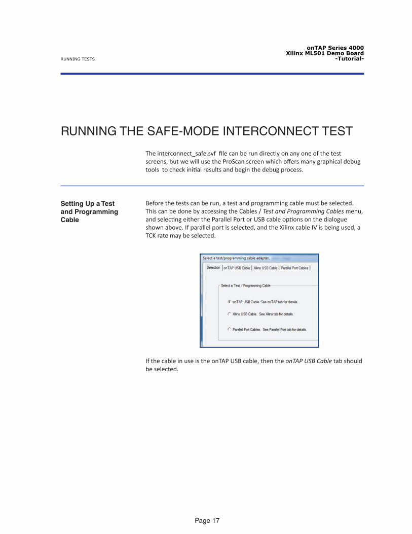
Setting Up a Test and Programming Cable
Before the tests can be run, a test and programming cable must be selected. This can be done by accessing the Cables / Test and Programming Cables menu, and selecting either the Parallel Port or USB cable options on the dialogue shown above. If parallel port is selected, and the Xilinx cable IV is being used, a TCK rate may be selected.
If the cable in use is the onTAP USB cable, then the onTAP USB Cable tab should be selected.
RUNNING TESTS

onTAP Series 4000Xilinx ML501 Demo Board
-Tutorial-
Page 18
The TCK rate can be adjusted with the slider control and the USB cable should appear in the Cable Name list.
These setups only need to be visited when the cable type changes or the TCK
rate needs to be adjusted
Setting Up a Test and Programming Cable(continued)
RUNNING TESTS
onTAP Series 4000Xilinx ML501 Demo Board
-Tutorial-
Page 19
THE PROSCAN SCREEN
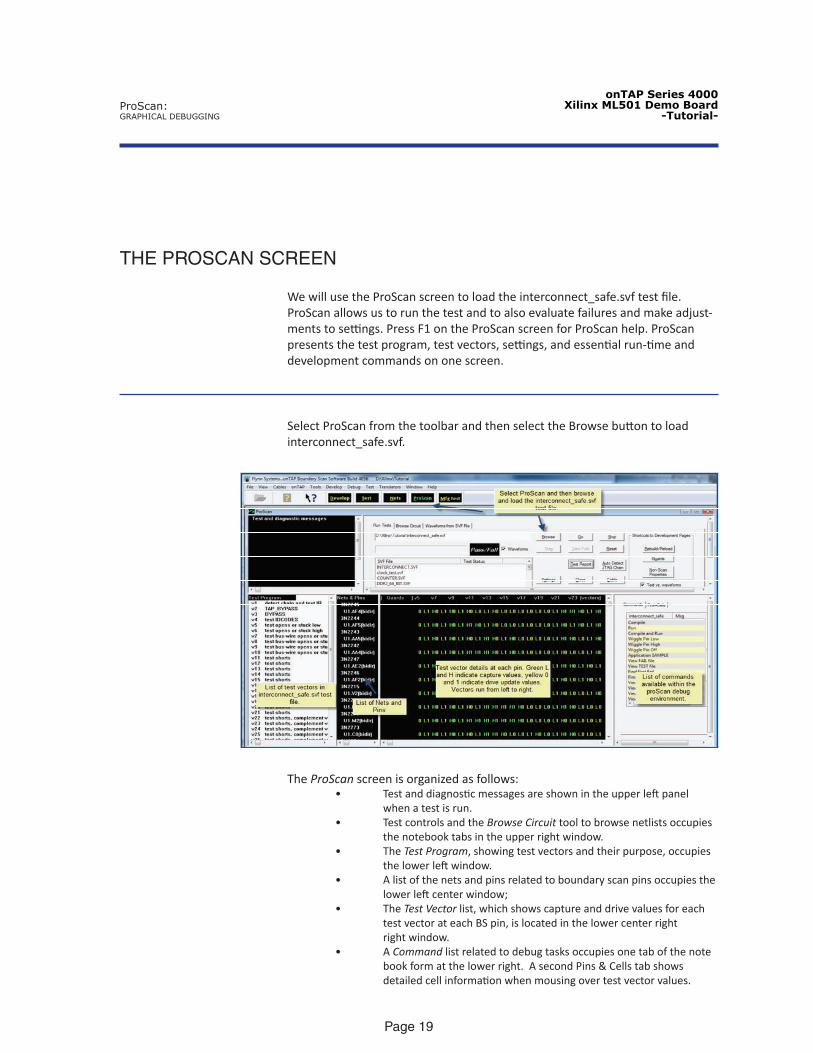
We will use the ProScan screen to load the interconnect_safe.svf test file. ProScan allows us to run the test and to also evaluate failures and make adjust-ments to settings. Press F1 on the ProScan screen for ProScan help. ProScan presents the test program, test vectors, settings, and essential run-time and development commands on one screen.
Select ProScan from the toolbar and then select the Browse button to load interconnect_safe.svf.
The ProScan screen is organized as follows:• Test and diagnostic messages are shown in the upper left panel when a test is run.• Test controls and the Browse Circuit tool to browse netlists occupies the notebook tabs in the upper right window.• The Test Program, showing test vectors and their purpose, occupies the lower left window.• A list of the nets and pins related to boundary scan pins occupies the lower left center window;• The Test Vector list, which shows capture and drive values for each test vector at each BS pin, is located in the lower center right right window. • A Command list related to debug tasks occupies one tab of the note book form at the lower right. A second Pins & Cells tab shows detailed cell information when mousing over test vector values.
ProScan:GRAPHICAL DEBUGGING
onTAP Series 4000Xilinx ML501 Demo Board
-Tutorial-
Page 20
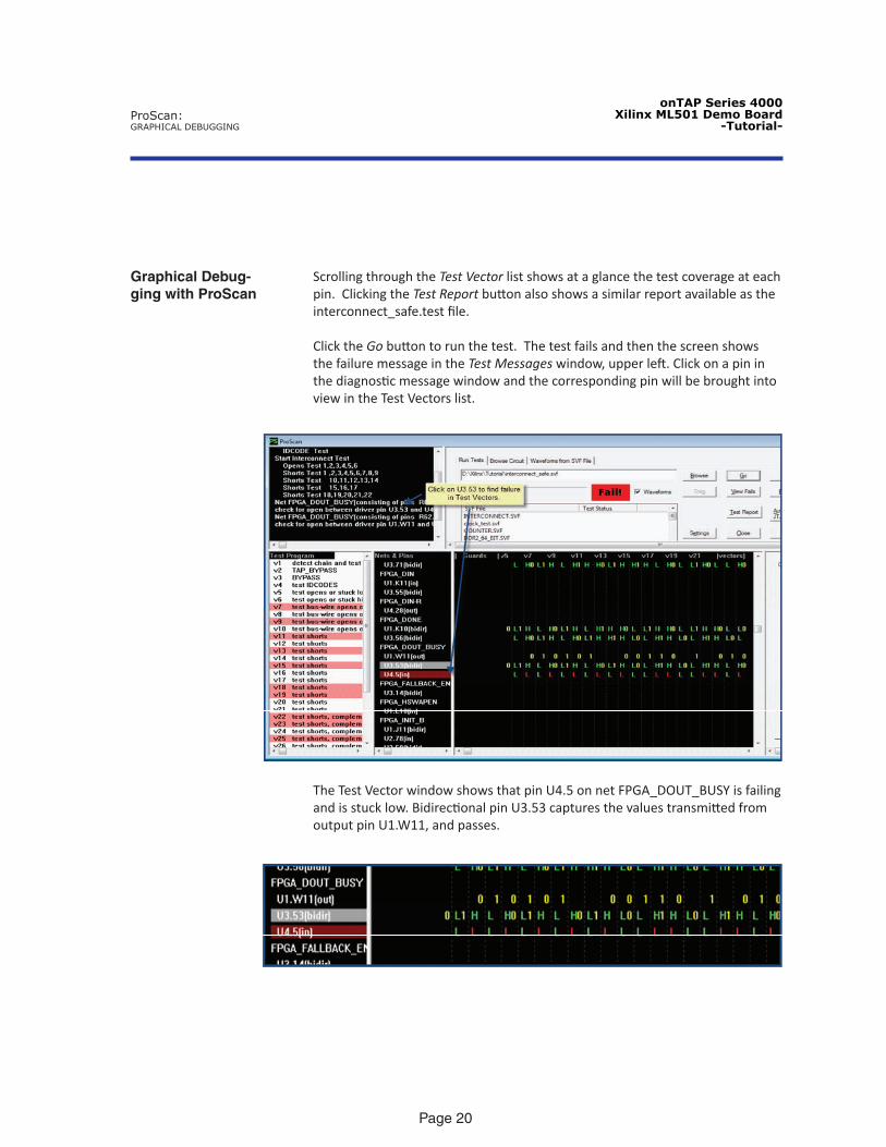
Scrolling through the Test Vector list shows at a glance the test coverage at each pin. Clicking the Test Report button also shows a similar report available as the interconnect_safe.test file. Click the Go button to run the test. The test fails and then the screen shows the failure message in the Test Messages window, upper left. Click on a pin in the diagnostic message window and the corresponding pin will be brought into view in the Test Vectors list.
Graphical Debug-ging with ProScan
The Test Vector window shows that pin U4.5 on net FPGA_DOUT_BUSY is failing and is stuck low. Bidirectional pin U3.53 captures the values transmitted from output pin U1.W11, and passes.
ProScan:GRAPHICAL DEBUGGING
onTAP Series 4000Xilinx ML501 Demo Board
-Tutorial-
Page 21
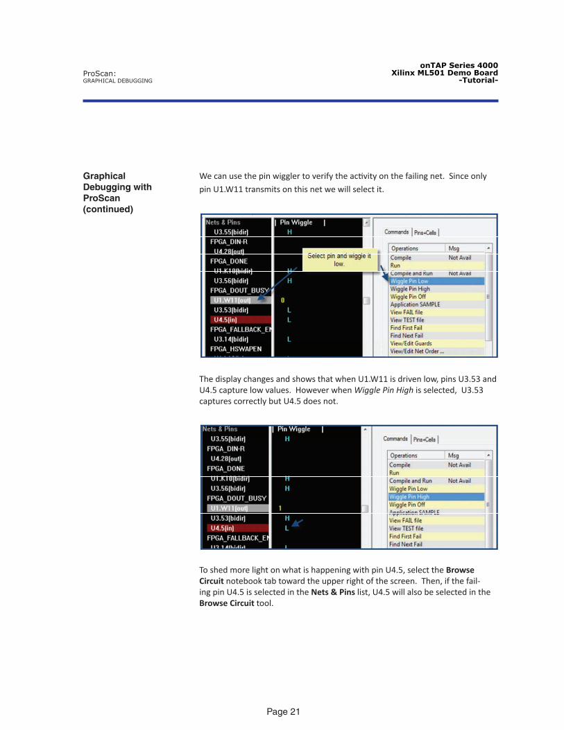
We can use the pin wiggler to verify the activity on the failing net. Since only
pin U1.W11 transmits on this net we will select it. Graphical Debugging with ProScan(continued)
The display changes and shows that when U1.W11 is driven low, pins U3.53 and U4.5 capture low values. However when Wiggle Pin High is selected, U3.53 captures correctly but U4.5 does not.
To shed more light on what is happening with pin U4.5, select the Browse Circuit notebook tab toward the upper right of the screen. Then, if the fail-ing pin U4.5 is selected in the Nets & Pins list, U4.5 will also be selected in the Browse Circuit tool.
ProScan:GRAPHICAL DEBUGGING
onTAP Series 4000Xilinx ML501 Demo Board
-Tutorial-
Page 22
Graphical Debugging with ProScan(continued)
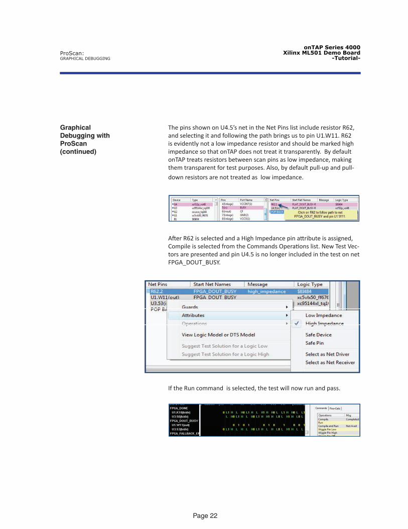
The pins shown on U4.5’s net in the Net Pins list include resistor R62, and selecting it and following the path brings us to pin U1.W11. R62 is evidently not a low impedance resistor and should be marked high impedance so that onTAP does not treat it transparently. By default onTAP treats resistors between scan pins as low impedance, making them transparent for test purposes. Also, by default pull-up and pull-
down resistors are not treated as low impedance.
After R62 is selected and a High Impedance pin attribute is assigned, Compile is selected from the Commands Operations list. New Test Vec-tors are presented and pin U4.5 is no longer included in the test on net FPGA_DOUT_BUSY.
If the Run command is selected, the test will now run and pass.
ProScan:GRAPHICAL DEBUGGING

onTAP Series 4000Xilinx ML501 Demo Board
-Tutorial-
Page 23
Enhancing Fault Coverage
Now that a basic safe test is passing, the next step will be to enhance the fault coverage. In safe test mode, nets having pins connected to undefined devices are not tested. Scrolling through the list of Test Vectors shows many pins with-out test vector activity.The procedure to enhance fault coverage is as follows:
• Browse through the Test Vectors and check for untested pins. Select them and then in the Browse Circuit tool note any unsafe devices that occur on their nets. In some case following a path through resis- tors and buffers may be necessary. • Select the unsafe device in the Net Pins list and right click for a menu Select Attributes and then select Safe Device. When only a pin and not the entire device should be marked safe, Safe Pin may be chosen. • Select Compile from the command list, and then select Run when Compile is done. If failures occur then the Safe attribute may need to be removed or guards may be required.
In this example, pin U1.AC12 is initially not tested. Selecting it and following the Circuit Browser leads to unsafe device U16. When the Safe Device attribute for
U16 is selected and the test is recompiled, U1.AC12 shows test vector activity.
Guards In some cases guards must be set in order to enable tests. In this example, the pins on the SRAM related nets are not selected because SRAM U19 is not considered safe. In order to mark U19 safe, a guard should be placed on its chip select line so that U19’s data bus is not inadvertently enabled during intercon-nect test pin activity. One way to check which pin should be guarded in this case is to select an un-tested pin on an SRAM net. If pin U1.AB17 is selected, then SRAM U19 is seen to be on its net. Selecting U19 in The Net Pins list leads back to U19. Browsing through U19’s pins brings up the CS pin, U19.98. Scan pin U1.AB24 is seen to drive U19.98 so a guard, DRIVE_HIGH, is applied to U1.AB24 to deselect U19. U19 can then be marked safe. The guard is set by right clicking on U1.AB24 and then selecting the Guards menu.
Flash device U20 is also seen to be attached to U1.AB17’s net so a similar proce-dure is followed to set a guard on its output enable pin, U20.32, to keep it high.
This procedure to add test coverage will be covered in the next few sections but first we will briefly introduce some of the other onTAP screens
ProScan:GRAPHICAL DEBUGGING
onTAP Series 4000Xilinx ML501 Demo Board
-Tutorial-
Page 24
THE TEST SCREEN
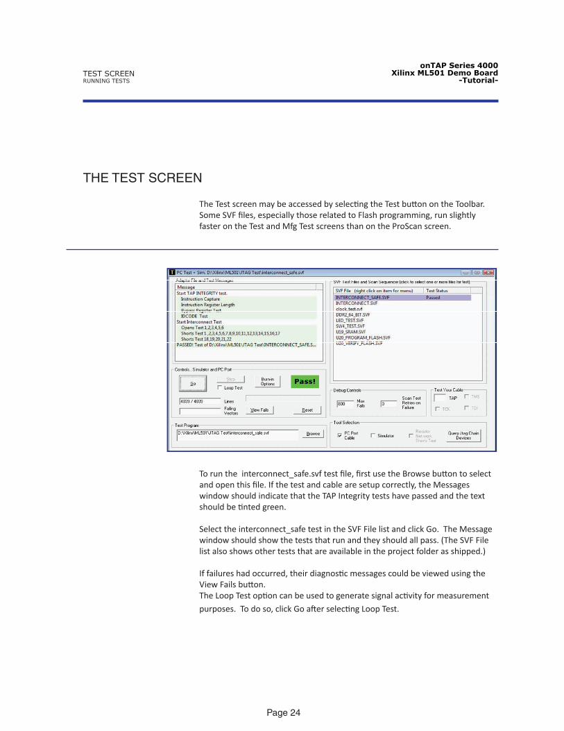
The Test screen may be accessed by selecting the Test button on the Toolbar. Some SVF files, especially those related to Flash programming, run slightly faster on the Test and Mfg Test screens than on the ProScan screen.
To run the interconnect_safe.svf test file, first use the Browse button to select and open this file. If the test and cable are setup correctly, the Messages window should indicate that the TAP Integrity tests have passed and the text should be tinted green.
Select the interconnect_safe test in the SVF File list and click Go. The Message window should show the tests that run and they should all pass. (The SVF File list also shows other tests that are available in the project folder as shipped.)
If failures had occurred, their diagnostic messages could be viewed using the View Fails button.The Loop Test option can be used to generate signal activity for measurement
purposes. To do so, click Go after selecting Loop Test.
TEST SCREENRUNNING TESTS
onTAP Series 4000Xilinx ML501 Demo Board
-Tutorial-
Page 25
NETLIST BROWSER SCREEN
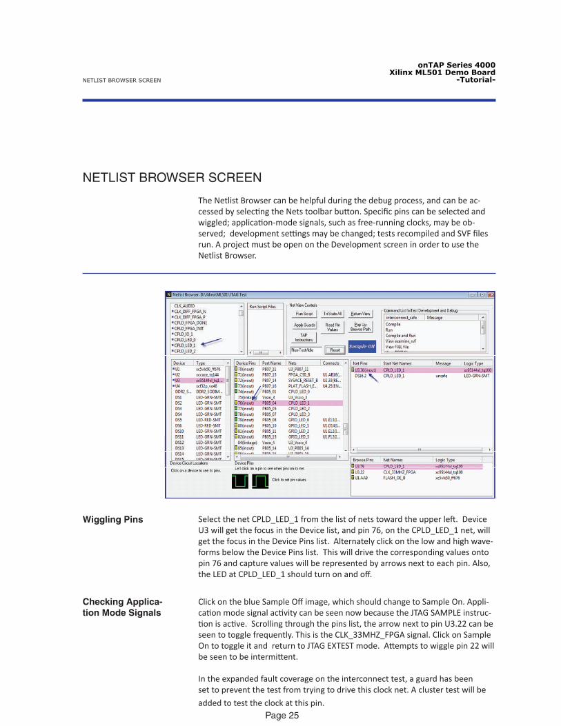
The Netlist Browser can be helpful during the debug process, and can be ac-cessed by selecting the Nets toolbar button. Specific pins can be selected and wiggled; application-mode signals, such as free-running clocks, may be ob-served; development settings may be changed; tests recompiled and SVF files run. A project must be open on the Development screen in order to use the Netlist Browser.
Select the net CPLD_LED_1 from the list of nets toward the upper left. Device U3 will get the focus in the Device list, and pin 76, on the CPLD_LED_1 net, will get the focus in the Device Pins list. Alternately click on the low and high wave-forms below the Device Pins list. This will drive the corresponding values onto pin 76 and capture values will be represented by arrows next to each pin. Also, the LED at CPLD_LED_1 should turn on and off.
Wiggling Pins
Click on the blue Sample Off image, which should change to Sample On. Appli-cation mode signal activity can be seen now because the JTAG SAMPLE instruc-tion is active. Scrolling through the pins list, the arrow next to pin U3.22 can be seen to toggle frequently. This is the CLK_33MHZ_FPGA signal. Click on Sample On to toggle it and return to JTAG EXTEST mode. Attempts to wiggle pin 22 will be seen to be intermittent.
In the expanded fault coverage on the interconnect test, a guard has been set to prevent the test from trying to drive this clock net. A cluster test will be
added to test the clock at this pin.
Checking Applica-tion Mode Signals
NETLIST BROWSER SCREEN
onTAP Series 4000Xilinx ML501 Demo Board
-Tutorial-
Page 26
COMPLETING THE INTERCONNECT TEST
A more comprehensive interconnect test can be built by reviewing the non-JTAG portions of the project assembly and proceeding as follows:
• Match models for non-JTAG devices such as resistor packs, buffers, transceiv ers, logic elements, and memory devices to the corresponding onTAP models. This is done on the Non-Scan page.• Set guards as required to control critical signals such as output enables on memory devices, power resets, and clocks. Guards may be set on the Guards page, the Net Browser, or from within ProScan.• Set the ’safe’ attribute once components have been checked and guards set as required. Also, when the safe disposition of all relevant components has been established then the Test Only Safe Circuits option on the TestGen page can be deselected. Attributes may be set on the Non-Scan page, the Net Browser, or from within ProScan.
This procedure was used to establish necessary settings and to complete the interconnect test, which is included in the project folder. Specific settings that were added to complete the interconnect test include:
• All of the resistor packs were assigned to a Non-JTAG model on the Non-Scan page.• Several additional guards were set:
o U1.AA9 OUTPUT_HIGHo U1.AA14 OUTPUT_OFF_INPUT_ONo U4.6 OUTPUT_OFF_INPUT_ON
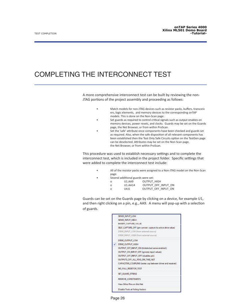
Guards can be set on the Guards page by clicking on a device, for example U1, and then right clicking on a pin, e.g., AA9. A menu will pop-up with a selection
of guards.
TEST COMPLETION
onTAP Series 4000Xilinx ML501 Demo Board
-Tutorial-
Page 27
o The guard selections work on a toggle basis and can be turned on and off. The DRIVE_OUTPUT_HIGH guard will hold the Flash device’s output enable pin high throughout the interconnect test, preventing contention on the Flash device’s (U20) data pins.
o Guards can also be set on the Netlist Browser and ProScan screens, which is sometimes more convenient during debug. Guards have been set for the following pins:
U1.AA9 OUTPUT_HIGH• U1.AA14 OUTPUT_OFF_INPUT_ON• U4.6 OUTPUT_OFF_INPUT_ON•
The PULLUP and PULLDOWN options were selected on the Settings • page.
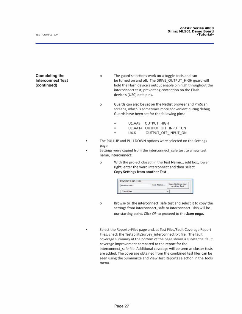
Settings were copied from the interconnect_safe test to a new test • name, interconnect:
o With the project closed, in the Test Name... edit box, lower right, enter the word interconnect and then select Copy Settings from another Test.
o Browse to the interconnect_safe test and select it to copy the settings from interconnect_safe to interconnect. This will be
our starting point. Click Ok to proceed to the Scan page.
• Select the Reports+Files page and, at Test Files/Fault Coverage Report Files, check the TestabilitySurvey_interconnect.txt file. The fault coverage summary at the bottom of the page shows a substantial fault coverage improvement compared to the report for the interconnect_safe file. Additional coverage will be seen as cluster tests are added. The coverage obtained from the combined test files can be seen using the Summarize and View Test Reports selection in the Tools menu.
TEST COMPLETION
Completing the Interconnect Test(continued)

onTAP Series 4000Xilinx ML501 Demo Board
-Tutorial-
Page 28
TEST AND DEBUG
Test Screen With the addition of guards, the interconnect.svf test should load and pass on the Test screen. Additional test activity is indicated by activity on the LEDs and the audio device.
Add some failures to check the test.
Set switch 8 on DIP switch SW4, to ON. This will cause a failure because the net at switch 8 will be connected to power, and a message will be shown in the Message window. The same message can be seen by clicking on the View Fails button. Set the switch back to OFF and rerun the test, which should now pass again.
On connector J4, connect pins 62 and 64 to create a short circuit fault. When the test is run, a diagnostic message will show the nets at pins 62 and 64 shorted.
TEST AND DEBUG
onTAP Series 4000Xilinx ML501 Demo Board
-Tutorial-
Page 29
ADDING CLUSTER TESTS…AN SRAM EXAMPLE
Cluster tests can test the connections between boundary scan pins and cluster device pins, and also check the basic functionality of the target parts. The fol-lowing cluster tests have been added, and all of the DTS models are included in the …/DTS Models subdirectory.
• An SRAM test for U19.• A DDR2 SDRAM test for the DDR2_SODIMM• Program and verify files for the Intel Strataflash, U20• A test to load “Welcome to onTAP” into an LCD.• An LED test• A DIP switch test for SW4• A clock test
The SRAM test will be reviewed next because it is representative of many memory cluster tests. All of the DTS cluster test models, using digital test syntax
(DTS), are included in the DTS Models subdirectory.
TEST DEVELOPMENT FOR SRAM U19
The target device in this test example is a pipelined IS61NLP25636A SRAM at circuit location U19.
Projects Page
CLUSTER TESTING
onTAP Series 4000Xilinx ML501 Demo Board
-Tutorial-
Page 30
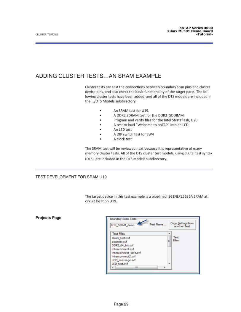
A standard procedure in setting up a new test is to copy settings from an exist-ing test and then modify them as appropriate in the new test. This can be done using the Copy Settings from another Test button. Enter a test name for the SRAM test, say U19_SRAM_demo, and then use Copy Settings to copy settings from the interconnect_safe test.Click Ok and the U19_SRAM_demo will open and all of the notebook page tab icons will be green. However, several key tasks remain in order to setup a test:
• Any components between U19’s pins and boundary scan pins must be modeled on the Non-Scan page so that onTAP can establish a path between cluster pins and their corrsponding scan I/O pins.• Guards must be adjusted so that all cluster device (U19) pins are controllable.• U19 has to be matched, on the Cluster page, to a DTS SRAM model.
Projects Page(continued)
Check Connections on U19’s Pins
The Net Browser can help show components that are connected to U19’s pins and that lie between U19 and scan I/O pins. Select the Nets toolbar button, and then select U19 in the Device list. Inspecting the Device Pins list shows resistor packs RP52 to RP59 lie between U19’s pins and pins on U1.
The procedure is to select a U19 pin, say U19.2, which brings up, in the Net Pins list, the pins connected on U19.2’s net. Then select RP52.8, which in turn will bring up the pins connected to RP52, revealing the connections to scan device U1.
The resistor packs RP52 to RP59 need to have a resistor pack model, OHMx4, assigned on the Development screen’s Non-Scan page. First though, while in the Net Browser, guards settings that may affect U19 can be checked.
CLUSTER TESTING
onTAP Series 4000Xilinx ML501 Demo Board
-Tutorial-
Page 31
Check Guards Settings
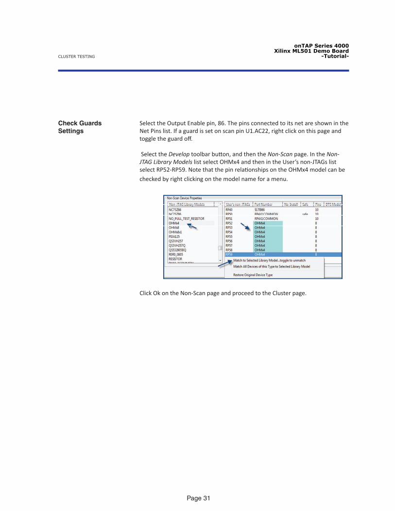
Select the Output Enable pin, 86. The pins connected to its net are shown in the Net Pins list. If a guard is set on scan pin U1.AC22, right click on this page and toggle the guard off.
Select the Develop toolbar button, and then the Non-Scan page. In the Non-JTAG Library Models list select OHMx4 and then in the User’s non-JTAGs list select RP52-RP59. Note that the pin relationships on the OHMx4 model can be
checked by right clicking on the model name for a menu.
Click Ok on the Non-Scan page and proceed to the Cluster page.
CLUSTER TESTING
onTAP Series 4000Xilinx ML501 Demo Board
-Tutorial-
Page 32
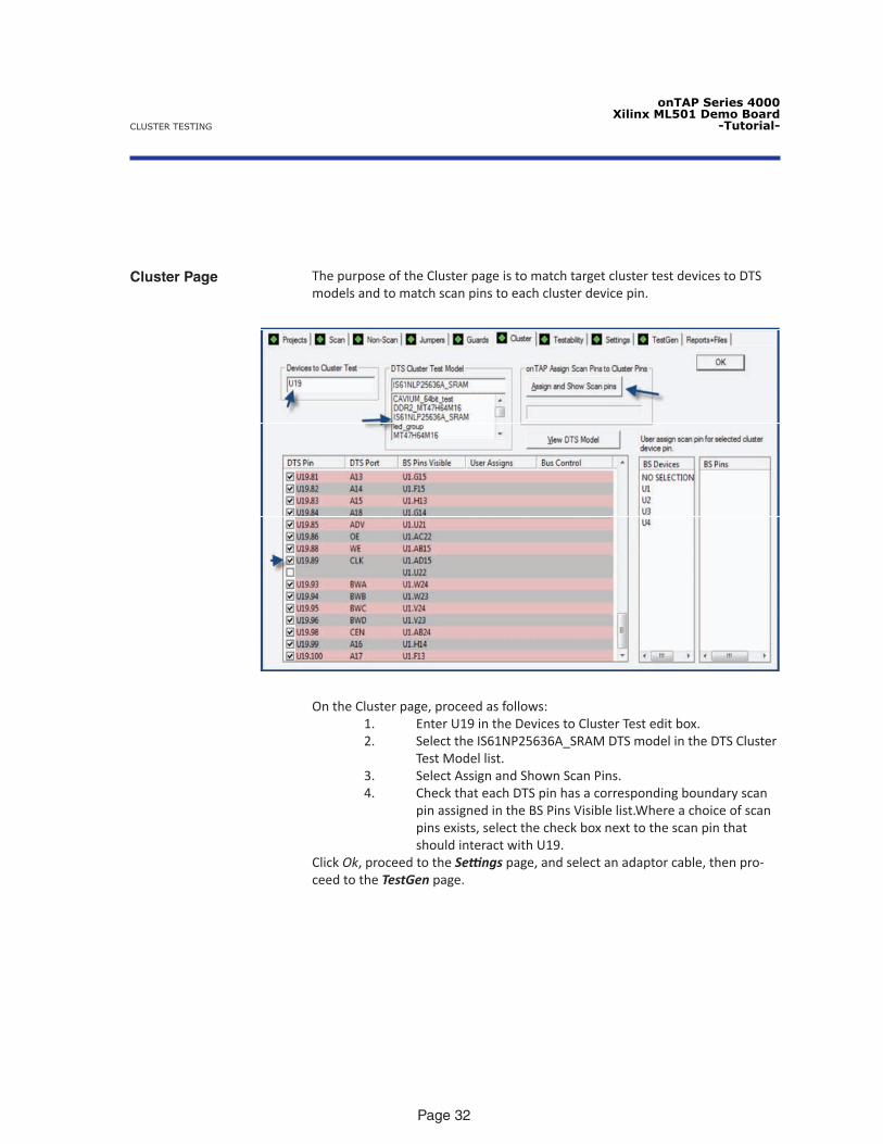
Cluster Page The purpose of the Cluster page is to match target cluster test devices to DTS models and to match scan pins to each cluster device pin.
On the Cluster page, proceed as follows:1. Enter U19 in the Devices to Cluster Test edit box.2. Select the IS61NP25636A_SRAM DTS model in the DTS Cluster Test Model list. 3. Select Assign and Shown Scan Pins.4. Check that each DTS pin has a corresponding boundary scan pin assigned in the BS Pins Visible list.Where a choice of scan pins exists, select the check box next to the scan pin that should interact with U19.
Click Ok, proceed to the Settings page, and select an adaptor cable, then pro-ceed to the TestGen page.
CLUSTER TESTING
onTAP Series 4000Xilinx ML501 Demo Board
-Tutorial-
Page 33
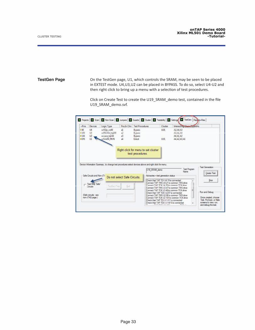
On the TestGen page, U1, which controls the SRAM, may be seen to be placed in EXTEST mode. U4,U3,U2 can be placed in BYPASS. To do so, select U4-U2 and then right click to bring up a menu with a selection of test procedures.
Click on Create Test to create the U19_SRAM_demo test, contained in the file U19_SRAM_demo.svf.
TestGen Page
CLUSTER TESTING
onTAP Series 4000Xilinx ML501 Demo Board
-Tutorial-
Page 34
Check and Run the U19_SRAM_demo Test
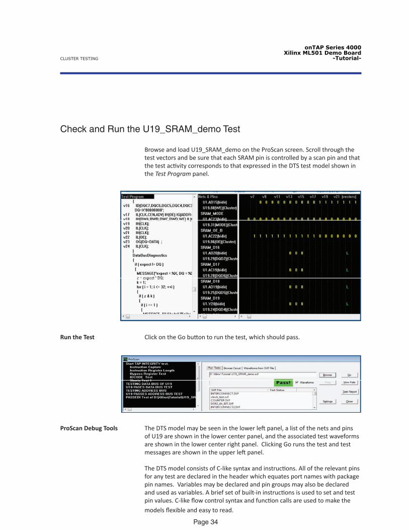
Browse and load U19_SRAM_demo on the ProScan screen. Scroll through the test vectors and be sure that each SRAM pin is controlled by a scan pin and that the test activity corresponds to that expressed in the DTS test model shown in the Test Program panel.
Run the Test Click on the Go button to run the test, which should pass.
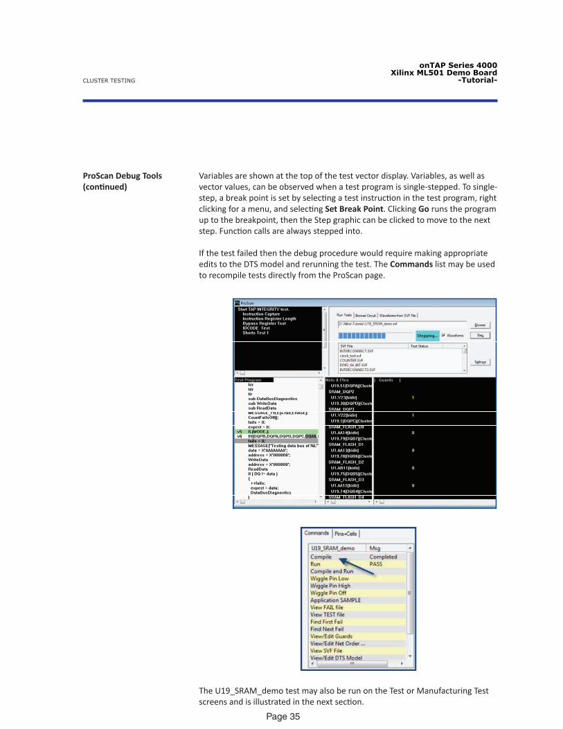
ProScan Debug Tools The DTS model may be seen in the lower left panel, a list of the nets and pins of U19 are shown in the lower center panel, and the associated test waveforms are shown in the lower center right panel. Clicking Go runs the test and test messages are shown in the upper left panel.
The DTS model consists of C-like syntax and instructions. All of the relevant pins for any test are declared in the header which equates port names with package pin names. Variables may be declared and pin groups may also be declared and used as variables. A brief set of built-in instructions is used to set and test pin values. C-like flow control syntax and function calls are used to make the
models flexible and easy to read.
CLUSTER TESTING
onTAP Series 4000Xilinx ML501 Demo Board
-Tutorial-
Page 35
ProScan Debug Tools(continued)
Variables are shown at the top of the test vector display. Variables, as well as vector values, can be observed when a test program is single-stepped. To single-step, a break point is set by selecting a test instruction in the test program, right clicking for a menu, and selecting Set Break Point. Clicking Go runs the program up to the breakpoint, then the Step graphic can be clicked to move to the next step. Function calls are always stepped into.
If the test failed then the debug procedure would require making appropriate edits to the DTS model and rerunning the test. The Commands list may be used to recompile tests directly from the ProScan page.
The U19_SRAM_demo test may also be run on the Test or Manufacturing Test screens and is illustrated in the next section.
CLUSTER TESTING
onTAP Series 4000Xilinx ML501 Demo Board
-Tutorial-
Page 36
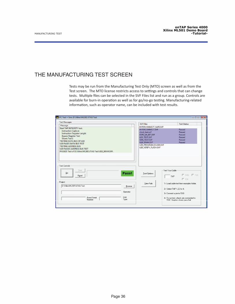
THE MANUFACTURING TEST SCREEN
Tests may be run from the Manufacturing Test Only (MTO) screen as well as from the Test screen. The MTO license restricts access to settings and controls that can change tests. Multiple files can be selected in the SVF Files list and run as a group. Controls are available for burn-in operation as well as for go/no-go testing. Manufacturing-related information, such as operator name, can be included with test results.
MANUFACTURING TEST
onTAP Series 4000Xilinx ML501 Demo Board
-Tutorial-
Page 37
SUMMARIZING TEST RESULTS
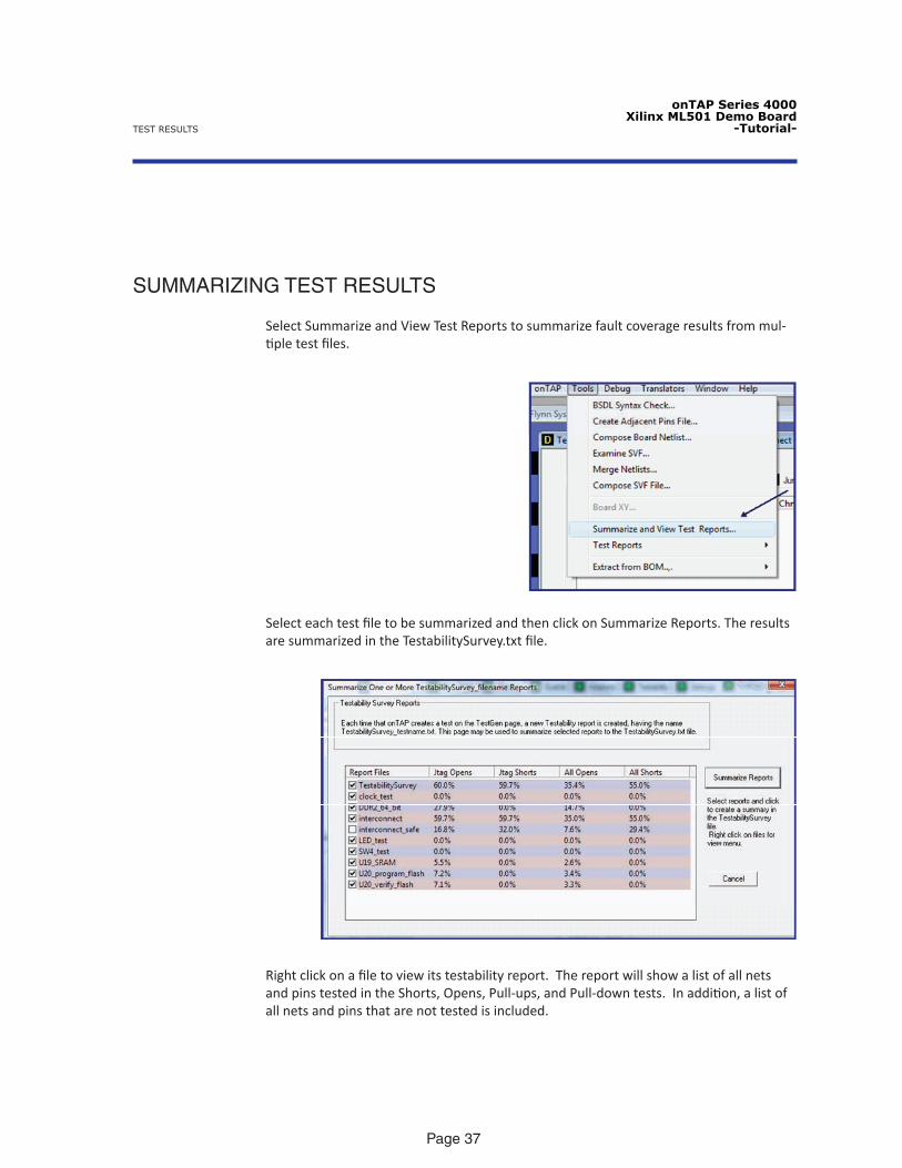
Select Summarize and View Test Reports to summarize fault coverage results from mul-tiple test files.
Select each test file to be summarized and then click on Summarize Reports. The results are summarized in the TestabilitySurvey.txt file.
Right click on a file to view its testability report. The report will show a list of all nets and pins tested in the Shorts, Opens, Pull-ups, and Pull-down tests. In addition, a list of all nets and pins that are not tested is included.
TEST RESULTS
onTAP Series 4000Xilinx ML501 Demo Board
-Tutorial-
Page 38
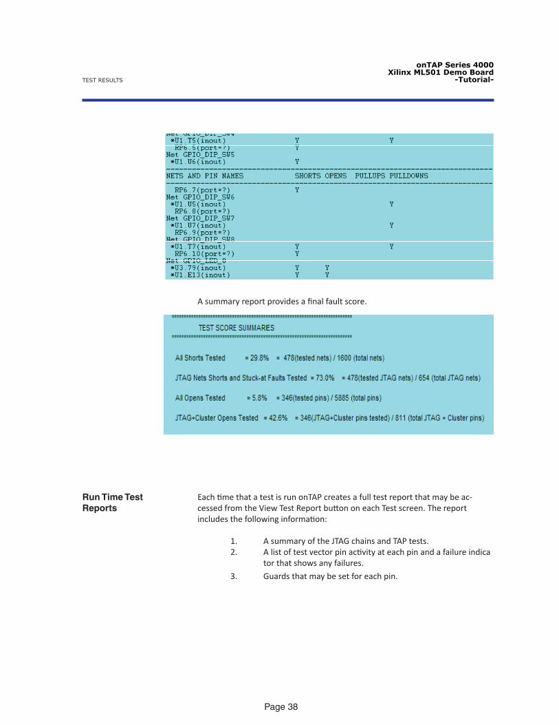
A summary report provides a final fault score.
Each time that a test is run onTAP creates a full test report that may be ac-cessed from the View Test Report button on each Test screen. The report includes the following information:
1. A summary of the JTAG chains and TAP tests.2. A list of test vector pin activity at each pin and a failure indica tor that shows any failures.
3. Guards that may be set for each pin.
Run Time Test Reports
TEST RESULTS
onTAP Series 4000Xilinx ML501 Demo Board
-Tutorial-
Page 39
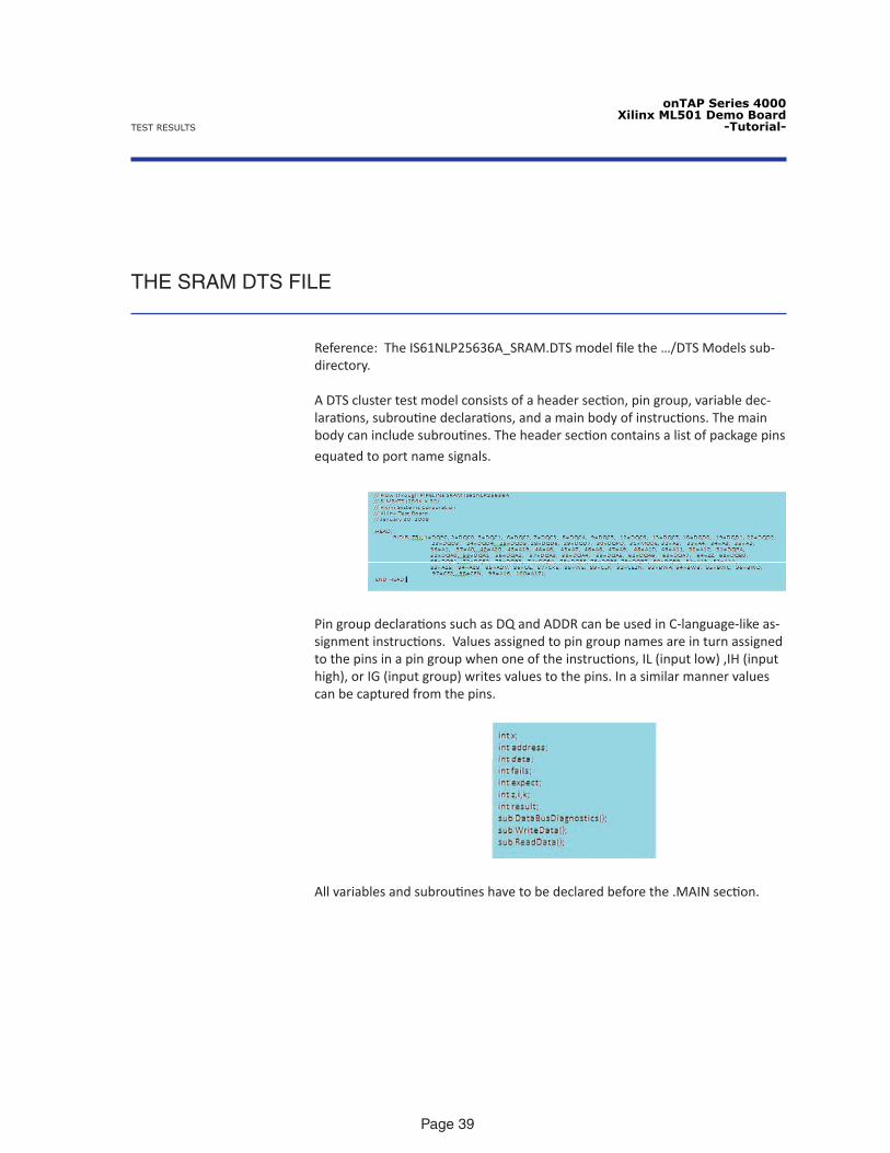
THE SRAM DTS FILE
Reference: The IS61NLP25636A_SRAM.DTS model file the …/DTS Models sub-directory.
A DTS cluster test model consists of a header section, pin group, variable dec-larations, subroutine declarations, and a main body of instructions. The main body can include subroutines. The header section contains a list of package pins
equated to port name signals.
Pin group declarations such as DQ and ADDR can be used in C-language-like as-signment instructions. Values assigned to pin group names are in turn assigned to the pins in a pin group when one of the instructions, IL (input low) ,IH (input high), or IG (input group) writes values to the pins. In a similar manner values can be captured from the pins.
All variables and subroutines have to be declared before the .MAIN section.
TEST RESULTS
onTAP Series 4000Xilinx ML501 Demo Board
-Tutorial-
Page 40
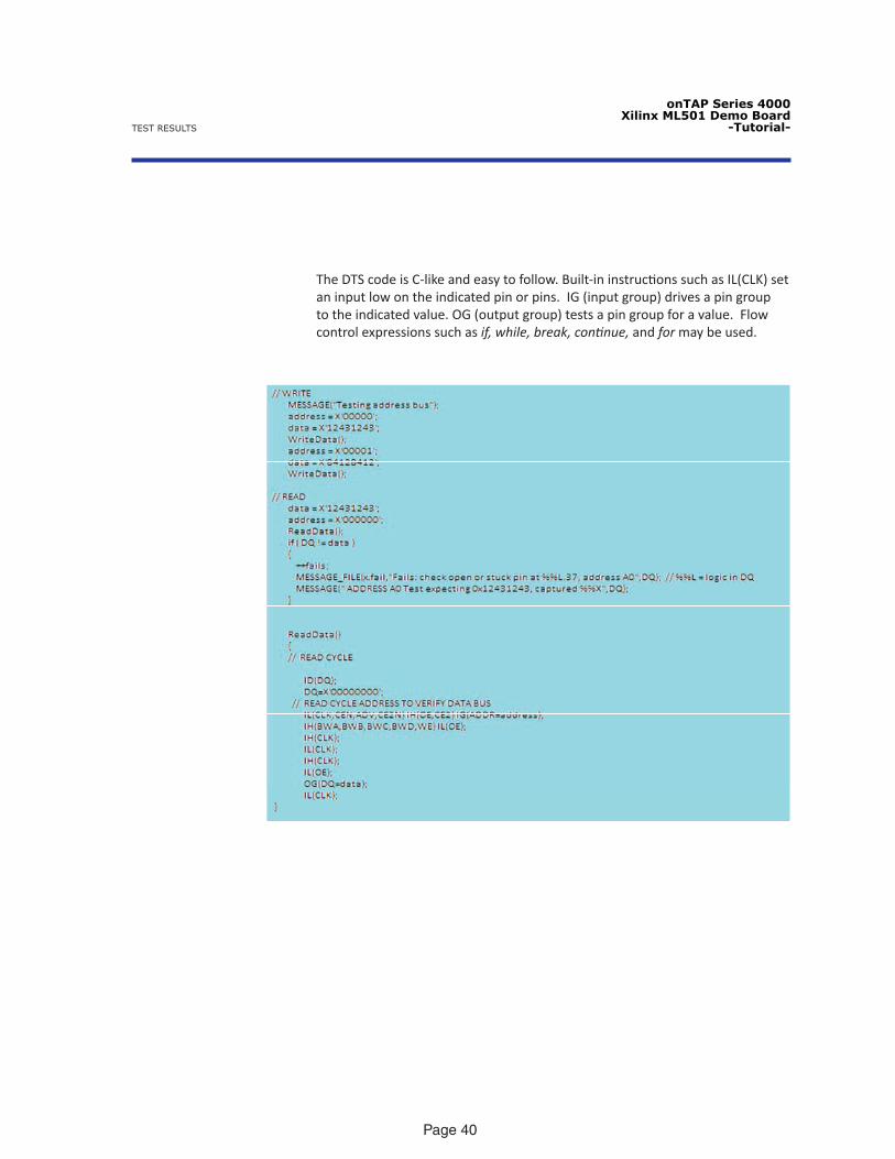
The DTS code is C-like and easy to follow. Built-in instructions such as IL(CLK) set an input low on the indicated pin or pins. IG (input group) drives a pin group to the indicated value. OG (output group) tests a pin group for a value. Flow control expressions such as if, while, break, continue, and for may be used.
TEST RESULTS