
Xilinx Constraints Guide Guide 2 UG625 (v 12.3) ... 110 ArchitectureSupport ... 194...
278
Constraints Guide UG625 (v 12.3) September 21, 2010
Transcript of Xilinx Constraints Guide Guide 2 UG625 (v 12.3) ... 110 ArchitectureSupport ... 194...
Constraints Guide
UG625 (v 12.3) September 21, 2010

Xilinx is disclosing this user guide, manual, release note, and/or specification (the “Documentation”) to yousolely for use in the development of designs to operate with Xilinx hardware devices. You may not reproduce,distribute, republish, download, display, post, or transmit the Documentation in any form or by any meansincluding, but not limited to, electronic, mechanical, photocopying, recording, or otherwise, without the priorwritten consent of Xilinx. Xilinx expressly disclaims any liability arising out of your use of the Documentation.Xilinx reserves the right, at its sole discretion, to change the Documentation without notice at any time. Xilinxassumes no obligation to correct any errors contained in the Documentation, or to advise you of any correctionsor updates. Xilinx expressly disclaims any liability in connection with technical support or assistance that may beprovided to you in connection with the Information.
THE DOCUMENTATION IS DISCLOSED TO YOU “AS-IS” WITH NOWARRANTY OF ANY KIND. XILINXMAKES NO OTHER WARRANTIES, WHETHER EXPRESS, IMPLIED, OR STATUTORY, REGARDINGTHE DOCUMENTATION, INCLUDING ANY WARRANTIES OF MERCHANTABILITY, FITNESS FOR APARTICULAR PURPOSE, OR NONINFRINGEMENT OF THIRD-PARTY RIGHTS. IN NO EVENT WILLXILINX BE LIABLE FOR ANY CONSEQUENTIAL, INDIRECT, EXEMPLARY, SPECIAL, OR INCIDENTALDAMAGES, INCLUDING ANY LOSS OF DATA OR LOST PROFITS, ARISING FROM YOUR USE OF THEDOCUMENTATION.
© Copyright 2002-2010 Xilinx Inc. All Rights Reserved. XILINX, the Xilinx logo, the Brand Window and otherdesignated brands included herein are trademarks of Xilinx, Inc. All other trademarks are the property of theirrespective owners. The PowerPC name and logo are registered trademarks of IBM Corp., and used under license.All other trademarks are the property of their respective owners.
Constraints Guide2 www.xilinx.com UG625 (v 12.3) September 21, 2010

Preface
About This GuideThe Constraints Guide describes constraints and attributes that can be attached to designsfor Xilinx® FPGA and CPLD devices. This chapter contains the following sections:• Guide Contents• Additional Resources• Conventions
Guide ContentsThis Guide contains the following chapters:• About this Guide discusses what is new in this Guide for the ISE® Design Suite and
provides other introductory information.• Constraint Types discusses the types of constraints documented within this Guide,
including CPLD fitter, grouping constraints, logical constraints, physical constraints,mapping directives, placement constraints, routing directives, synthesis constraints,and timing constraints
• Entry Strategies for Xilinx Constraints discusses entry strategies for Xilinxconstraints, including how to use ISE Design Suite to enter a given constraint type.
• Timing Constraint Strategies provides general guidelines that explain how toconstrain the timing on designs when using the implementation tools for FPGAdevices.
• Xilinx Constraints describes the individual constraints that can be used with Xilinx®FPGA and CPLD devices, including, for each constraint, architecture support,applicable elements, description, propagation rules, syntax examples, and, wherenecessary, additional information for particular constraints.
Additional ResourcesTo find additional documentation, see the Xilinx website at:
http://www.xilinx.com/literature.
To search the Answer Database of silicon, software, and IP questions and answers, or tocreate a technical support WebCase, see the Xilinx website at:
http://www.xilinx.com/support.
ConventionsThis document uses the following conventions. An example illustrates each convention.
Constraints GuideUG625 (v 12.3) September 21, 2010 www.xilinx.com 3

Preface: About This Guide
TypographicalThe following typographical conventions are used in this document:
Convention Meaning or Use ExampleCourier font Messages, prompts, and
program files that the systemdisplays
speed grade: - 100
Courier bold Literal commands that youenter in a syntactical statement
ngdbuild design_name
Helvetica bold Commands that you selectfrom a menu
File > Open
Keyboard shortcuts Ctrl+C
Italic font Variables in a syntaxstatement for which youmust supply values
ngdbuild design_name
References to other manuals See the Command LineTools User Guide for moreinformation.
Emphasis in text If a wire is drawn so that itoverlaps the pin of a symbol,the two nets are not connected.
Square brackets [ ] An optional entry orparameter. However, inbus specifications, such asbus[7:0], they are required.
ngdbuild [option_name]design_name
Braces { } A list of items from which youmust choose one or more
lowpwr ={on|off}
Vertical bar | Separates items in a list ofchoices
lowpwr ={on|off}
Vertical ellipsis Repetitive material that hasbeen omitted
IOB #1: Name = QOUTIOB #2: Name = CLKIN
.
.
.
Horizontal ellipsis . . . Repetitive material that hasbeen omitted
allow block . . .block_name loc1 loc2 ... locn;
Online DocumentThe following conventions are used in this document:
Convention Meaning or Use ExampleBlue text Cross-reference link See the section Additional
Resources for details.
Refer to Title Formats inChapter 1 for details.
See Figure 2-5 in the Virtex®-6Handbook.
Constraints Guide4 www.xilinx.com UG625 (v 12.3) September 21, 2010

Table of ContentsPreface About This Guide ...........................................................................................3
Guide Contents ...................................................................................................... 3Additional Resources............................................................................................. 3Conventions ........................................................................................................... 3
Typographical ................................................................................................... 4Online Document............................................................................................... 4
Chapter 1 Constraint Types.......................................................................................17Attributes and Constraints .................................................................................. 17
Attributes........................................................................................................ 17Implementation Constraints ............................................................................. 18
CPLD Fitter........................................................................................................... 18Grouping Constraints for Timing ....................................................................... 19
Using Predefined Groups ................................................................................. 19Predefined Group Examples ............................................................................. 20BRAMS_PORTA and BRAMS_PORTB Examples ............................................... 20
Logical Constraints .............................................................................................. 21Physical Constraints............................................................................................. 21Mapping Directives ............................................................................................. 22Placement Constraints ......................................................................................... 22
Relative Location (RLOC) Constraints ............................................................... 23Placement Constraints...................................................................................... 23
Routing Directives ............................................................................................... 23Synthesis Constraints .......................................................................................... 23Timing Constraints .............................................................................................. 24
XST Timing Constraints ................................................................................... 24Command Line Switch ..................................................................................... 24Constraints File................................................................................................ 25UCF Timing Constraint Support ....................................................................... 25From-To .......................................................................................................... 25OFFSET IN ...................................................................................................... 25OFFSET OUT................................................................................................... 25TIG ................................................................................................................. 25TIMEGRP........................................................................................................ 26TNM............................................................................................................... 26TNM Net......................................................................................................... 26Timing Model.................................................................................................. 26Priority ........................................................................................................... 26Timing and Grouping Constraints .................................................................... 27
Configuration Constraints ................................................................................... 28List of Configuration Constraints ...................................................................... 28
Chapter 2 Entry Strategies for Xilinx Constraints ...................................................29Constraints Entry Methods.................................................................................. 29
Constraints GuideUG625 (v 12.3) September 21, 2010 www.xilinx.com 5
Constraints Entry Table ....................................................................................... 30Schematic Design................................................................................................. 32VHDL Attributes.................................................................................................. 33Verilog Attributes................................................................................................. 33
Verilog Limitations .......................................................................................... 34Verilog Meta Comments ................................................................................... 34
User Constraints File (UCF)................................................................................. 34UCF Flow........................................................................................................ 35Manual Entry of Timing Constraints ................................................................. 35Constraint Conflicts in Multiple UCF Files......................................................... 35
User Constraints File (UCF) and Netlist Constraints File (NCF) FileSyntax ........................................................................................................... 35General Rules for UCF and NCF ....................................................................... 36Conflict in Constraints...................................................................................... 36Syntax............................................................................................................. 36Specifying Attributes for TIMEGRP and TIMESPEC........................................... 36Using Reserved Words ..................................................................................... 37Wildcards........................................................................................................ 37Traversing Hierarchies ..................................................................................... 37Entering Multiple Constraints........................................................................... 38File Name........................................................................................................ 38Instances and Blocks ........................................................................................ 39
Physical Constraints File (PCF) ........................................................................... 39Netlist Constraints File (NCF)............................................................................. 40Constraints Editor ................................................................................................ 40
Input/Output................................................................................................... 40Starting Constraints Editor ............................................................................... 41Running Constraints Editor From ISE Design Suite ........................................... 41Running Constraints Editor As a Standalone Tool .............................................. 41Running Constraints Editor From the Command Line With No Data
Loaded ..................................................................................................... 41Running Constraints Editor From the Command Line With the NGD File
Loaded ..................................................................................................... 41Running Constraints Editor From the Command Line With the NGD File and
the UCF File Loaded.................................................................................. 41Running Constraints Editor From the Command Line As a Background
Process ..................................................................................................... 42
ISE Design Suite .................................................................................................. 42PlanAhead ............................................................................................................ 42
Assigning Placement Constraints ...................................................................... 42Defining I/O Pin Configurations ....................................................................... 43Pin Assignment Overview................................................................................ 43Reviewing I/O Pin Data Information ................................................................. 43Pin Assignment ............................................................................................... 44I/O Planner Documentation .............................................................................. 44Floorplanning and Placement Constraints ......................................................... 45Placement LOC Constraint Assignment............................................................. 45Area Group Assignment................................................................................... 45
Setting Constraints in the Pinout & Area Constraints Editor (PACE) .............. 45Partial Design Pin Preassignment....................................................................... 45FPGA Editor ......................................................................................................... 47
Constraints Guide6 www.xilinx.com UG625 (v 12.3) September 21, 2010

Locked Nets and Components .......................................................................... 47Interaction Between Constraints........................................................................ 48
XST Constraint File (XCF) ................................................................................... 48Constraints Priority.............................................................................................. 48
File Priorities ................................................................................................... 49Timing Specification Priorities .......................................................................... 49OFFSET Priorities ............................................................................................ 49MAXSKEW and MAXDELAY Priorities............................................................. 49Constraints Priority Exceptions......................................................................... 50Constraint Set Interaction ................................................................................. 50
Chapter 3 Timing Constraint Strategies...................................................................51Basic Constraints Methodology .......................................................................... 51Input Timing Constraints .................................................................................... 52
Input Timing Constraints Overview.................................................................. 52System Synchronous Inputs.............................................................................. 52Source Synchronous Inputs .............................................................................. 54
Register-to-Register Timing Constraints ............................................................ 55Register-to-Register Timing Constraints Overview............................................. 56Automatically Related DCM/PLL/MMCM Clocks .............................................. 56Manually Related Clock Domains ..................................................................... 57Asynchronous Clock Domains.......................................................................... 58
Output Timing Constraints ................................................................................. 58Output Timing Constraints Overview ............................................................... 59System Synchronous Output ............................................................................ 59Source Synchronous Outputs............................................................................ 61
Exception Timing Constraints ............................................................................. 62Exception Timing Constraints Overview ........................................................... 62False Paths ...................................................................................................... 62Multi-Cycle Paths ............................................................................................ 63
Chapter 4 Xilinx Constraints .....................................................................................65Constraint Information........................................................................................ 65Alphabetized List of Xilinx Constraints ............................................................. 65AREA_GROUP (Area Group) ............................................................................. 68
Architecture Support........................................................................................ 68Applicable Elements ........................................................................................ 68Propagation Rules............................................................................................ 68Constraint Syntax ............................................................................................ 69Defining From Timing Groups.......................................................................... 75
ASYNC_REG (Asynchronous Register).............................................................. 76Architecture Support........................................................................................ 76Applicable Elements ........................................................................................ 76Propagation Rules............................................................................................ 76
BEL (BEL).............................................................................................................. 77Architecture Support........................................................................................ 77Applicable Elements ........................................................................................ 77Propagation Rules............................................................................................ 77
BLKNM (Block Name)......................................................................................... 79Architecture Support........................................................................................ 79
Constraints GuideUG625 (v 12.3) September 21, 2010 www.xilinx.com 7
Applicable Elements ........................................................................................ 79Propagation Rules............................................................................................ 79
BUFG (BUFG)....................................................................................................... 81Architecture Support........................................................................................ 81Applicable Elements ........................................................................................ 81Propagation Rules............................................................................................ 81
Clock Dedicated Route (CLOCK_DEDICATED_ROUTE) ................................ 82Architecture Support........................................................................................ 83Applicable Elements ........................................................................................ 83Propagation Rules............................................................................................ 83
COLLAPSE (Collapse) ......................................................................................... 83Architecture Support........................................................................................ 83Applicable Elements ........................................................................................ 84Propagation Rules............................................................................................ 84
COMPGRP (Component Group) ........................................................................ 84Architecture Support........................................................................................ 84Applicable Elements ........................................................................................ 85
CONFIG_MODE (Configuration Mode) ............................................................ 85Architecture Support........................................................................................ 85Applicable Elements ........................................................................................ 85Propagation Rules............................................................................................ 85
COOL_CLK (CoolCLOCK).................................................................................. 86Architecture Support........................................................................................ 86Applicable Elements ........................................................................................ 86Propagation Rules............................................................................................ 86
DATA_GATE (Data Gate) .................................................................................... 87Architecture Support........................................................................................ 88Applicable Elements ........................................................................................ 88Propagation Rules............................................................................................ 88
DCI Cascade (DCI_CASCADE) .......................................................................... 89Architecture Support........................................................................................ 89Applicable Elements ........................................................................................ 89Propagation Rules............................................................................................ 89
DCI Value (DCI_VALUE) .................................................................................... 90Architecture Support........................................................................................ 90Applicable Elements ........................................................................................ 90Propagation Rules............................................................................................ 90
Default (DEFAULT) ............................................................................................. 91Architecture Support........................................................................................ 91Applicable Elements ........................................................................................ 91Propagation Rules............................................................................................ 91Constraint Syntax ............................................................................................ 91
DIFF_TERM (Diff_Term)..................................................................................... 94Architecture Support........................................................................................ 94Applicable Elements ........................................................................................ 94PlanAhead™ Syntax ........................................................................................ 95
DIRECTED_ROUTING (Directed Routing) ...................................................... 95Architecture Support........................................................................................ 95Applicable Elements ........................................................................................ 95Propagation Rules............................................................................................ 95
Constraints Guide8 www.xilinx.com UG625 (v 12.3) September 21, 2010

DISABLE (Disable) .............................................................................................. 97Architecture Support........................................................................................ 97Applicable Elements ........................................................................................ 97Propagation Rules............................................................................................ 97
DRIVE (Drive)...................................................................................................... 98Architecture Support........................................................................................ 98Applicable Elements ........................................................................................ 98Propagation Rules............................................................................................ 98
DROP_SPEC (Drop Specifications) .................................................................. 100Architecture Support.......................................................................................100Applicable Elements .......................................................................................100Propagation Rules...........................................................................................100
ENABLE (Enable) ............................................................................................... 101Architecture Support.......................................................................................101Applicable Elements .......................................................................................101Propagation Rules...........................................................................................101
ENABLE_SUSPEND (Enable Suspend)............................................................ 102Architecture Support.......................................................................................102Applicable Elements .......................................................................................102Propagation Rules...........................................................................................102
FAST (Fast) ......................................................................................................... 103Architecture Support.......................................................................................103Applicable Elements .......................................................................................103Propagation Rules...........................................................................................103
FEEDBACK (Feedback) ..................................................................................... 105Architecture Support.......................................................................................105Applicable Elements .......................................................................................105Propagation Rules...........................................................................................105
FILE (File) ........................................................................................................... 106Architecture Support.......................................................................................106Applicable Elements .......................................................................................106Propagation Rules...........................................................................................106
FLOAT (Float)..................................................................................................... 107Architecture Support.......................................................................................107Applicable Elements .......................................................................................107Propagation Rules...........................................................................................108
FROM-THRU-TO (From Thru To) .................................................................... 108Architecture Support.......................................................................................109Applicable Elements .......................................................................................109Propagation Rules...........................................................................................109
FROM-TO (From To).......................................................................................... 110Architecture Support.......................................................................................110Applicable Elements .......................................................................................110Propagation Rules...........................................................................................110
FSM_STYLE (FSM Style)................................................................................... 112HBLKNM (Hierarchical Block Name) .............................................................. 112
Architecture Support.......................................................................................112Applicable Elements .......................................................................................112Propagation Rules...........................................................................................113
Constraints GuideUG625 (v 12.3) September 21, 2010 www.xilinx.com 9

HIODELAY_GROUP (HIODELAY Group) ...................................................... 114Architecture Support.......................................................................................114Applicable Elements .......................................................................................114Propagation Rules...........................................................................................114
Hierarchical Lookup Table Name (HLUTNM)................................................. 115Architecture Support.......................................................................................115HLUTNM Applicable Elements .......................................................................116Propagation Rules...........................................................................................116
H_SET (H Set) .................................................................................................... 117HU_SET (HU Set)............................................................................................... 117
Architecture Support.......................................................................................117Applicable Elements .......................................................................................118Propagation Rules...........................................................................................118
IBUF_DELAY_VALUE (Input Buffer Delay Value).......................................... 119Architecture Support.......................................................................................119Applicable Elements .......................................................................................119
IFD_DELAY_VALUE (IFD Delay Value) .......................................................... 121Architecture Support.......................................................................................121Applicable Elements .......................................................................................121Propagation Rules...........................................................................................121
IN_TERM (In Term) ........................................................................................... 122Architecture Support.......................................................................................122Applicable Elements .......................................................................................122Propagation Rules...........................................................................................122PlanAhead™ Syntax .......................................................................................124
INREG (Input Registers) ................................................................................... 124Architecture Support.......................................................................................124Applicable Elements .......................................................................................124Propagation Rules...........................................................................................124
Internal Vref Bank (INTERNAL_VREF_BANK).............................................. 125Architecture Support.......................................................................................125Applicable Elements .......................................................................................125Propagation Rules...........................................................................................125
IOB (IOB)............................................................................................................ 125Architecture Support.......................................................................................126Applicable Elements .......................................................................................126Propagation Rules...........................................................................................126
IOBDELAY (Input Output Block Delay) .......................................................... 127Architecture Support.......................................................................................128Applicable Elements .......................................................................................128Propagation Rules...........................................................................................128
IODELAY_GROUP (IODELAY Group) ............................................................ 128Architecture Support.......................................................................................128Applicable Elements .......................................................................................129Propagation Rules...........................................................................................129
IOSTANDARD (Input Output Standard) ........................................................ 129IOSTANDARD for FPGA Devices ....................................................................129IOSTANDARD for CPLD Devices ....................................................................130Architecture Support.......................................................................................130Applicable Elements .......................................................................................130
Constraints Guide10 www.xilinx.com UG625 (v 12.3) September 21, 2010

Propagation Rules...........................................................................................130
KEEP (Keep) ....................................................................................................... 132Architecture Support.......................................................................................132Applicable Elements .......................................................................................132Propagation Rules...........................................................................................132
KEEP_HIERARCHY (Keep Hierarchy)............................................................. 133Architecture Support.......................................................................................134Applicable Elements .......................................................................................135Propagation Rules...........................................................................................135
Keeper (KEEPER) ............................................................................................... 136Architecture Support.......................................................................................136Applicable Elements .......................................................................................136Propagation Rules...........................................................................................136
LOC (Location) ................................................................................................... 137LOC Description for FPGA Devices..................................................................137LOC Description for CPLD Devices..................................................................139LOC Priority...................................................................................................139Architecture Support.......................................................................................140Applicable Elements .......................................................................................140Propagation Rules...........................................................................................140Constraint Syntax ...........................................................................................140Digital Clock Manager (DCM) Constraint Examples..........................................143Flip-Flop Constraint Examples.........................................................................144I/O Constraint Examples .................................................................................145IOB Constraint Examples ................................................................................145Mapping Constraint Examples (FMAP) ............................................................145Multiplier Constraint Examples ......................................................................146ROM Constraint Examples ..............................................................................147Block RAM (RAMBs) Constraint Examples.......................................................147Slice Constraint Examples ...............................................................................148Slices Prohibited .............................................................................................149
LOCATE (Locate)................................................................................................ 149Architecture Support.......................................................................................150Applicable Elements .......................................................................................150Propagation Rules...........................................................................................150
LOCK_PINS (Lock Pins).................................................................................... 150Architecture Support.......................................................................................151Applicable Elements .......................................................................................151Propagation Rules...........................................................................................151
LUTNM (Lookup Table Name) ......................................................................... 152Architecture Support.......................................................................................152Applicable Elements .......................................................................................152Propagation Rules...........................................................................................152
MAP (Map) ......................................................................................................... 154Architecture Support.......................................................................................154Applicable Elements .......................................................................................154Propagation Rules...........................................................................................155
MAX_FANOUT (Max Fanout)........................................................................... 155Architecture Support.......................................................................................156Applicable Elements .......................................................................................156Propagation Rules...........................................................................................156
MAXDELAY (Maximum Delay) ........................................................................ 157
Constraints GuideUG625 (v 12.3) September 21, 2010 www.xilinx.com 11

Architecture Support.......................................................................................157Applicable Elements .......................................................................................157Propagation Rules...........................................................................................157
MAXPT (Maximum Product Terms) ................................................................. 160Architecture Support.......................................................................................160Applicable Elements .......................................................................................160Propagation Rules...........................................................................................160
MAXSKEW (Maximum Skew) .......................................................................... 161Architecture Support.......................................................................................161Applicable Elements .......................................................................................161Propagation Rules...........................................................................................161
MCB Performance (MCB_PERFORMANCE)................................................... 163MIODELAY_GROUP (MIODELAY Group)..................................................... 163
Architecture Support.......................................................................................163Applicable Elements .......................................................................................164Propagation Rules...........................................................................................164
NODELAY (No Delay) ....................................................................................... 164Architecture Support.......................................................................................164Applicable Elements .......................................................................................164Propagation Rules...........................................................................................165
NOREDUCE (No Reduce) ................................................................................. 166Architecture Support.......................................................................................166Applicable Elements .......................................................................................166Propagation Rules...........................................................................................166
OFFSET IN (Offset In)....................................................................................... 167Architecture Support.......................................................................................167Applicable Elements .......................................................................................167
OFFSET OUT (Offset Out) ................................................................................ 172Architecture Support.......................................................................................172Applicable Elements .......................................................................................172
Open Drain (OPEN_DRAIN) ............................................................................ 176Architecture Support.......................................................................................176Applicable Elements .......................................................................................176Propagation Rules...........................................................................................176
OUT_TERM (Out Term) .................................................................................... 177Architecture Support.......................................................................................178Applicable Elements .......................................................................................178Propagation Rules...........................................................................................178PlanAhead™ Syntax .......................................................................................179
PERIOD (Period)................................................................................................ 179Architecture Support.......................................................................................180Applicable Elements .......................................................................................180Propagation Rules...........................................................................................180......................................................................................................................180PERIOD Specifications on CLKDLLs, DCMs, PLLs, and MMCMs ......................186
PIN (Pin) ............................................................................................................. 188Architecture Support.......................................................................................188Applicable Elements .......................................................................................188Propagation Rules...........................................................................................188
Post CRC (POST_CRC)...................................................................................... 188
Constraints Guide12 www.xilinx.com UG625 (v 12.3) September 21, 2010
Architecture Support.......................................................................................189Applicable Elements .......................................................................................189Propagation Rules...........................................................................................189
Post CRC Action (POST_CRC_ACTION) ........................................................ 189Architecture Support.......................................................................................189Applicable Elements .......................................................................................189Propagation Rules...........................................................................................189
Post CRC Frequency (POST_CRC_FREQ)........................................................ 190Architecture Support.......................................................................................191Applicable Elements .......................................................................................191Propagation Rules...........................................................................................191
Post CRC INIT Flag (POST_CRC_INIT_FLAG) .............................................. 191Architecture Support.......................................................................................192Applicable Elements .......................................................................................192Propagation Rules...........................................................................................192
Post CRC Signal (POST_CRC_SIGNAL) ......................................................... 192Architecture Support.......................................................................................192Applicable Elements .......................................................................................192Propagation Rules...........................................................................................192
Post CRC Source (POST_CRC_SOURCE) ........................................................ 193Architecture Support.......................................................................................193Applicable Elements .......................................................................................193Propagation Rules...........................................................................................193
PRIORITY (Priority) .......................................................................................... 194Architecture Support.......................................................................................194Applicable Elements .......................................................................................194Propagation Rules...........................................................................................194
PROHIBIT (Prohibit) ......................................................................................... 194Architecture Support.......................................................................................196Applicable Elements .......................................................................................196Propagation Rules...........................................................................................196
PULLDOWN (Pulldown)................................................................................... 197Architecture Support.......................................................................................197Applicable Elements .......................................................................................197Propagation Rules...........................................................................................197
PULLUP (Pullup) ............................................................................................... 199Architecture Support.......................................................................................199Applicable Elements .......................................................................................199Propagation Rules...........................................................................................199
PWR_MODE (Power Mode).............................................................................. 200Architecture Support.......................................................................................200Applicable Elements .......................................................................................200Propagation Rules...........................................................................................200
REG (Registers) .................................................................................................. 202Architecture Support.......................................................................................202Applicable Elements .......................................................................................202Propagation Rules...........................................................................................202
Relative Location (RLOC).................................................................................. 203Architecture Support.......................................................................................204Applicable Elements .......................................................................................204
Constraints GuideUG625 (v 12.3) September 21, 2010 www.xilinx.com 13

Propagation Rules...........................................................................................204Constraint Syntax ...........................................................................................205Using RPM Grid .............................................................................................205Set Modifiers ..................................................................................................206Linking Sets....................................................................................................207Modifying Sets ...............................................................................................208Using RLOCs with Xilinx Macros.....................................................................212Guidelines for Specifying Relative Locations.....................................................214Relative Location RLOC Sets ...........................................................................216
RLOC_ORIGIN (Relative Location Origin) ..................................................... 221Architecture Support.......................................................................................221Applicable Elements .......................................................................................221Propagation Rules...........................................................................................221Constraint Syntax ...........................................................................................221
RLOC_RANGE (Relative Location Range)....................................................... 223Architecture Support.......................................................................................223Applicable Elements .......................................................................................223Propagation Rules...........................................................................................223Constraint Syntax ...........................................................................................223
SAVE NET FLAG (Save Net Flag) ..................................................................... 225Architecture Support.......................................................................................225Applicable Elements .......................................................................................226Propagation Rules...........................................................................................226
SCHMITT_TRIGGER (Schmitt Trigger) .......................................................... 227Architecture Support.......................................................................................227Applicable Elements .......................................................................................227Propagation Rules...........................................................................................227
SIM Collision Check (SIM_COLLISION_CHECK)......................................... 228Architecture Support.......................................................................................228Applicable Elements .......................................................................................228Propagation Rules...........................................................................................228
SLEW (Slew)....................................................................................................... 229Architecture Support.......................................................................................229Applicable Elements .......................................................................................229Propagation Rules...........................................................................................229
SLOW (Slow)...................................................................................................... 231Architecture Support.......................................................................................231Applicable Elements .......................................................................................231Propagation Rules...........................................................................................231
STEPPING (Stepping) ....................................................................................... 233Architecture Support.......................................................................................233Applicable Elements .......................................................................................233Propagation Rules...........................................................................................233
SUSPEND (Suspend) ......................................................................................... 233Architecture Support.......................................................................................233Applicable Elements .......................................................................................234Propagation Rules...........................................................................................234
SYSTEM_JITTER (System Jitter) ...................................................................... 235Architecture Support.......................................................................................235Applicable Elements .......................................................................................235Propagation Rules...........................................................................................235
Constraints Guide14 www.xilinx.com UG625 (v 12.3) September 21, 2010
TEMPERATURE (Temperature) ........................................................................ 236Architecture Support.......................................................................................237Applicable Elements .......................................................................................237Propagation Rules...........................................................................................237
TIG (Timing Ignore) .......................................................................................... 237Architecture Support.......................................................................................238Applicable Elements .......................................................................................238Propagation Rules...........................................................................................238
TIMEGRP (Timing Group)................................................................................ 240Architecture Support.......................................................................................240Applicable Elements .......................................................................................240Propagation Rules...........................................................................................240
TIMESPEC (Timing Specifications) .................................................................. 246Architecture Support.......................................................................................246Applicable Elements .......................................................................................246Propagation Rules...........................................................................................246Constraint Syntax ...........................................................................................246
TNM (Timing Name) ......................................................................................... 248Architecture Support.......................................................................................249Applicable Elements .......................................................................................249Propagation Rules...........................................................................................249
TNM_NET (Timing Name Net)......................................................................... 253Architecture Support.......................................................................................253Applicable Elements .......................................................................................253Rules..............................................................................................................253Propagation Rules...........................................................................................254
TPSYNC (Timing Point Synchronization)........................................................ 256Architecture Support.......................................................................................256Applicable Elements .......................................................................................256Propagation Rules...........................................................................................257
TPTHRU (Timing Thru Points)......................................................................... 259Architecture Support.......................................................................................259Applicable Elements .......................................................................................259Propagation Rules...........................................................................................259
TSidentifier (Timing Specification Identifier) .................................................. 261Architecture Support.......................................................................................261Applicable Elements .......................................................................................261Propagation Rules...........................................................................................261
U_SET (U SET) ................................................................................................... 264Architecture Support.......................................................................................264Applicable Elements .......................................................................................264Propagation Rules...........................................................................................264
Use Internal VREF (USE_INTERNAL_VREF).................................................. 266Architecture Support.......................................................................................266Applicable Elements .......................................................................................266Propagation Rules...........................................................................................266
USE_LUTNM (Use LUTNM)............................................................................. 267Architecture Support.......................................................................................267Applicable Elements .......................................................................................267Propagation Rules...........................................................................................267
Constraints GuideUG625 (v 12.3) September 21, 2010 www.xilinx.com 15

USE_RLOC (Use Relative Location) ................................................................. 268Architecture Support.......................................................................................268Applicable Elements .......................................................................................268Propagation Rules...........................................................................................268
Use Low Skew Lines (USELOWSKEWLINES) ................................................ 271Architecture Support.......................................................................................271Applicable Elements .......................................................................................271Propagation Rules...........................................................................................271
VCCAUX (VCCAUX)......................................................................................... 272Architecture Support.......................................................................................273Applicable Elements .......................................................................................273
VOLTAGE (Voltage)........................................................................................... 273Architecture Support.......................................................................................273Applicable Elements .......................................................................................273Propagation Rules...........................................................................................274
VREF (VREF) ...................................................................................................... 274Architecture Support.......................................................................................274Applicable Elements .......................................................................................274Propagation Rules...........................................................................................274
WIREAND (Wire And) ...................................................................................... 275Architecture Support.......................................................................................275Applicable Elements .......................................................................................275Propagation Rules...........................................................................................275
XBLKNM (XBLKNM) ........................................................................................ 276Architecture Support.......................................................................................277Applicable Elements .......................................................................................277Propagation Rules...........................................................................................277
Constraints Guide16 www.xilinx.com UG625 (v 12.3) September 21, 2010

Chapter 1
Constraint TypesThis chapter discusses constraint types documented in this Guide. This chapter containsthe following sections:
• Attributes and Constraints
• CPLD Fitter
• Grouping Constraints
• Logical Constraints
• Physical Constraints
• Mapping Directives
• Placement Constraints
• Routing Directives
• Synthesis Constraints
• Timing Constraints
• Configuration Constraints
Attributes and ConstraintsSome designers use the terms attribute and constraint interchangeably. Other designersgive them different meanings. In addition, certain language constructs use the termsattribute and directive in similar, but not identical, senses. Xilinx® uses the terms attributesand constraints as defined below.
AttributesAn attribute is a property associated with a device architecture primitive componentthat generally affects an instantiated components functionality or implementation.Attributes are passed as follows:
• In VHDL, by means of generic maps
• In Verilog, by means of defparams or inline parameter passing while instantiatingthe primitive component
Examples of attributes are:
• The INIT property on a LUT4 component
• The CLKFX_DIVIDE property on a DCM
All attributes are described in the appropriate Xilinx Libraries Guides as a part of theprimitive component description.
Constraints GuideUG625 (v 12.3) September 21, 2010 www.xilinx.com 17

Chapter 1: Constraint Types
Implementation ConstraintsImplementation constraints are instructions given to the FPGA implementation tools todirect the mapping, placement, timing or other guidelines for the implementation toolsto follow while processing an FPGA design. Implementation constraints are generallyplaced in the User Constraints File (UCF), but may exist in the Hardware DescriptionLanguage (HDL) code, or in a synthesis constraints file. Examples of implementationconstraints are:• LOC (placement) constraints• PERIOD (timing) constraints
The Constraints Guide documents implementation constraints.
CPLD FitterThe following constraints apply to CPLD devices:
BUFG (CPLD)
Collapse (COLLAPSE)
CoolCLOCK (COOL_CLK)
Data Gate (DATA_GATE)
Fast (FAST)
Input Registers (INREG)
Input Output Standard (IOSTANDARD)
Keep (KEEP)
Keeper (KEEPER)
Location (LOC)
Maximum Product Terms (MAXPT)
No Reduce (NOREDUCE)
Offset In (OFFSET IN)
Offset Out (OFFSET OUT)
Open Drain (OPEN_DRAIN)
Period (PERIOD)
Prohibit (PROHIBIT)
Pullup (PULLUP)
Power Mode (PWR_MODE)
Registers (REG)
Schmitt Trigger (SCHMITT_TRIGGER)
Slow (SLOW)
Timing Group (TIMEGRP)
Timing Specifications (TIMESPEC)
Timing Name (TNM)
Timing Specification Identifier (TSidentifier)
VREF
Constraints Guide18 www.xilinx.com UG625 (v 12.3) September 21, 2010

Chapter 1: Constraint Types
Wire And (WIREAND)
Grouping Constraints for TimingFor a Timing Specifications (TIMESPEC)constraint, specify the set of paths to beanalyzed by grouping start and end points in one of the following ways.
• Refer to a predefined group by specifying one of the corresponding keywords:CPUS, DSPS, FFS, HSIOS, LATCHES, MULTS, PADS, RAMS, BRAMS_PORTA, orBRAMS_PORTB.
• Create your own groups within a predefined group by tagging symbols withTNM (Timing Name) (pronounced tee-name) and TNM_NET (Timing Name Net)constraints.
• Create groups that are combinations of existing groups using TIMEGRP (TimingGroup) symbols.
• Create groups by pattern matching on net names. For more information, seeCreating Groups by Pattern Matching in the TIMEGRP (Timing Group) constraint.
Using Predefined GroupsUsing predefined groups, you can refer to a group of flip-flops, input latches, pads, orRAMs by using the corresponding keywords.
Predefined Groups KeywordsKeyword DescriptionCPUS PPC405 in Virtex®-4 FX devices
DSPS DSP48 and any DSP48 derivative in Virtex-4 devices, Virtex-5 devices, and Spartan®-3AExtended devices
CPUS in Virtex-5 FXT devices
FFS All CLB and IOB edge-triggered flip-flops and Shift Register LUTs (all devices haveshift register LUTs)
HSIOS GT11 (Virtex-4 devices), GTP_DUAL (Virtex-5 devices) and GTX_DUAL ( Virtex-5 FXTdevices)
LATCHES All CLB and IOB level-sensitive latches
MULTS Synchronous and asynchronous multipliers.
PADS All I/O pads (typically inferred from top level HDL ports)
RAMS – All CLB LUT RAMs, both single- and dual-port (includes both ports of dual-port)
– All block RAMs, both single-and dual-port (includes both ports of dual-port)
– FIFOS – All FIFO (First In, First Out) Block RAM Memory
BRAMS_PORTA Port A of all dual-port block RAMs
BRAMS_PORTB Port B of all dual-port block RAMs
From-To statements enable you to define timing specifications for paths betweenpredefined groups. The following examples are TS constraints that are entered inthe UCF. This method enables you to easily define default timing specifications, asillustrated by the following examples.
Constraints GuideUG625 (v 12.3) September 21, 2010 www.xilinx.com 19

Chapter 1: Constraint Types
Predefined Group ExamplesFollowing is a UCF syntax example.
TIMESPEC "TS01"=FROM FFS TO FFS 30;
TIMESPEC "TS02"=FROM LATCHES TO LATCHES 25;
TIMESPEC "TS03"=FROM PADS TO RAMS 70;
TIMESPEC "TS04"=FROM FFS TO PADS 55;
TIMESPEC "TS01" = FROM BRAMS_PORTA TO BRAMS_PORTB(gork*);
For BRAMS_PORTA and BRAM_PORTB, the specification TS01 controls paths that beginat any A port and end at a B port, which drives a signal matching the pattern gork*.
BRAMS_PORTA and BRAMS_PORTB ExamplesFollowing are additional examples of BRAMS_PORTA and BRAMS_PORTB.
NET "X" TNM_NET = BRAMS_PORTA groupA;
The TNM group groupA contains all A ports that are driven by net X. If net X is tracedforward into any B port inputs, any single-port block RAM elements, or any Select RAMelements, these do not become members of groupA.
NET "X" TNM_NET = BRAMS_PORTB( dob* ) groupB;
The TNM group groupB contains each B port driven by net X, if at least one output onthat B port drives a signal matching the pattern dob*.
INST "Y" TNM = BRAMS_PORTB groupC;
The TNM group groupC contains all B ports found under instance Y. If instance Y isitself a dual-port block RAM primitive, then groupC contains the B port of that instance.
INST "Y" TNM = BRAMS_PORTA( doa* ) groupD;
The TNM group groupD contains each A port found under instance Y, if at least oneoutput on that A port drives a signal matching the pattern doa*.
TIMEGRP "groupE" = BRAMS_PORTA;
The user group groupE contains the A ports of all dual-port block RAM elements. Thisis equivalent to BRAMS_PORTA ( * ).
TIMEGRP "groupF" = BRAMS_PORTB( mem/dob* );
The user group groupF contains all B ports, which drives a signal matching the patternmem/dob*.
A predefined group can also carry a name qualifier. The qualifier can appear any placethe predefined group is used. This name qualifier restricts the number of elementsreferred to. The syntax is:
predefined group (name_qualifier [ name_qualifier ])
name_qualifier is the full hierarchical name of the net that is sourced by the primitivebeing identified.
The name qualifier can include the following wildcard characters:• An asterisk (*) to show any number of characters• A question mark (?) to show a single character
Wildcard characters allow you to:• Specify more than one net• Shorten and simplify the full hierarchical name
Constraints Guide20 www.xilinx.com UG625 (v 12.3) September 21, 2010

Chapter 1: Constraint Types
For example, specifying the group FFS(MACRO_A/Q?) selects only the flip-flops drivingthe Q0, Q1, Q2 and Q3 nets.
Grouping ConstraintsComponent Group(COMPGRP)
Pin (PIN) Timing Group (TIMEGRP)
Timing Name (TNM) Timing Name Net(TNM_NET)
Timing Point Synchronization(TPSYNC)
Timing Thru Points(TPTHRU)
Logical ConstraintsLogical constraints are constraints that are attached to elements before mapping orfitting. Logical constraints help adapt design performance to expected worst-caseconditions. Later, when you choose a specific Xilinx® architecture, and Place and Routeor fit your design, the logical constraints are converted into physical constraints.
You can attach logical constraints using attributes in the input design, which are writteninto the Netlist Constraints File (NCF) or NGC netlist, or with a User Constraints File(UCF).
Three categories of logical constraints are:• Placement Constraints• Relative Location (RLOC) Constraints• Timing Constraints
For FPGA devices, Relative Location (RLOC) constraints group logic elements intodiscrete sets. They allow you to define the location of any element within the set relativeto other elements in the set, regardless of eventual placement in the overall design. Formore information, see Relative Location (RLOC).
Timing constraints allow you to specify the maximum allowable delay or skew on anygiven set of paths or nets in your design.
Physical ConstraintsNote The information in this section applies to FPGA devices only.
Constraints can also be attached to the elements in the physical design, that is, the designafter mapping has been performed. These constraints are called physical constraints.They are defined in the Physical Constraints File (PCF) created during mapping.
Xilinx® recommends that you place user-generated constraints in the User ConstraintsFile (UCF) file, not in an NCF or Physical Constraints File (PCF) file.
When a design is mapped, the logical constraints found in the netlist and the UCF fileare translated into physical constraints, that is, constraints that apply to a specificarchitecture. These constraints are found in a mapper-generated file called the PhysicalConstraints File (PCF).
The PCF file contains two sections:• The schematic section, which contains the physical constraints based on the logical
constraints found in the netlist and the UCF file• The user section, which can be used to add any physical constraints
Constraints GuideUG625 (v 12.3) September 21, 2010 www.xilinx.com 21

Chapter 1: Constraint Types
Mapping DirectivesMapping directives instruct the mapper to perform specific operations. The constraintsshown in the following table are mapping directives.
Mapping DirectivesArea Group (AREA_GROUP) BEL Block Name (BLKNM)
DCI_VALUE Drive (DRIVE) Fast (FAST)
Hierarchical Block Name (HBLKNM) Hierarchical Lookup Table Name(HLUTNM)
HU_SET
IOB Input Output Block Delay (IOBDELAY) Input Output Standard(IOSTANDARD)
Keep (KEEP) Keeper (KEEPER) Lookup Table Name (LUTNM)
Map (MAP) No Delay (NODELAY) Pulldown (PULLDOWN)
Pullup (PULLUP) Relative Location (RLOC) Relative Location Origin(RLOC_ORIGIN)
Relative Location Range(RLOC_RANGE)
Save Net Flag (SAVE NET FLAG) Slew (SLEW)
U_SET Use Relative Location (USE_RLOC) XBLKNM
Placement ConstraintsThis section describes the placement constraints for each type of logic element in FPGAdesigns, such as:• Flip-flops• ROMs and RAMs• BUFTs• CLBs• IOBs• I/Os• Edge decoders• Global buffers
Individual logic gates, such as AND or OR gates, are mapped into CLB functiongenerators before the constraints are read, and therefore cannot be constrained.
The following constraints control mapping and placement of symbols in a netlist:• Block Name (BLKNM)• Hierarchical Block Name (HBLKNM)• Hierarchical Lookup Table Name (HLUTNM)• Location (LOC)• Lookup Table Name (LUTNM)• Prohibit (PROHIBIT)• Relative Location (RLOC)• Relative Location Origin (RLOC_ORIGIN)• Relative Location Range (RLOC_RANGE)• XBLKNM
Constraints Guide22 www.xilinx.com UG625 (v 12.3) September 21, 2010

Chapter 1: Constraint Types
Most constraints can be specified either in the Hardware Description Language (HDL)or in the User Constraints File (UCF) file. In a constraints file, each placement constraintacts upon one or more symbols. Every symbol in a design carries a unique name, whichis defined in the input file. Use this name in a constraint statement to identify the symbol.
The User Constraints File (UCF) and Netlist Constraints File (NCF) files are casesensitive. Identifier names (names of objects, such as net names) must exactly match thecase of the name as it exists in the source design netlist. However, any Xilinx® constraintkeyword (for example, LOC, PROHIBIT, RLOC, BLKNM) can be entered in either alluppercase or all lowercase letters. Mixed case is not allowed.
Relative Location (RLOC) ConstraintsThe Relative Location Origin (RLOC_ORIGIN) constraint groups logic elements intodiscrete sets. You can define the location of any element within the set relative to otherelements in the set, regardless of eventual placement in the overall design. For example,if RLOC constraints are applied to a group of eight flip-flops organized in a column,the mapper maintains the columnar order and moves the entire group of flip-flops as asingle unit. In contrast, absolute Location (LOC) constraints constrain design elementsto specific locations on the FPGA die with no relation to other design elements.
Placement ConstraintsThe following constraints are placement constraints:• Area Group (AREA_GROUP)• BEL• Location (LOC)• Locate (LOCATE)• Prohibit (PROHIBIT)• Relative Location (RLOC)• Relative Location Origin (RLOC_ORIGIN)• Relative Location Range (RLOC_RANGE)• Use Relative Location (USE_RLOC)
Routing DirectivesRouting directives instruct PAR to perform specific operations. The following constraintsare routing directives:• Area Group (AREA_GROUP)• Configuration Mode (CONFIG_MODE)• Lock Pins (LOCK_PINS)
Synthesis ConstraintsSynthesis constraints direct the synthesis tool optimization technique for a particulardesign or piece of Hardware Description Language (HDL) code. The constraints areeither embedded in the source code, or are included in a separate synthesis constraintsfile. Examples of synthesis constraints are:• USE_DSP48 (XST)• RAM_STYLE (XST)
Constraints GuideUG625 (v 12.3) September 21, 2010 www.xilinx.com 23
Chapter 1: Constraint Types
XST synthesis constraints are documented in the XST User Guide. Other synthesisconstraints are documented in the software vendor’s documentation.
The following constraints are synthesis constraints:
• From To (FROM-TO)
• IOB
• Keep (KEEP)
• Map (MAP)
• Offset In (OFFSET IN)
• Offset Out (OFFSET OUT)
• Period (PERIOD)
• Timing Ignore (TIG)
• Timing Name (TNM)
• Timing Name Net (TNM_NET)
Timing ConstraintsThe Xilinx® software enables you to specify precise timing requirements for your Xilinxdesigns. These requirements can be specified using global or path specific timingconstraints. The recommended method for defining the constraints for common timingrequirement scenarios is discussed in Chapter 5, Timing Constraint Strategies.
The primary way to specify timing constraints is to enter them in the User ConstraintsFile (UCF). In addition, constraints can be entered in the source (HDL and Schematic).For detailed information on each constraint, see the later chapters of this guide.
Once you define timing specifications and map the design, PAR places and routes yourdesign based on these requirements.
To analyze the results of your timing specifications, use the command line tool, TRACE(TRCE) or the Timing Analyzer.
XST Timing ConstraintsXST supports an XST Constraint File (XCF) syntax to define synthesis and timingconstraints. Xilinx no longer supports the constraint syntax in use before ISE® DesignSuite release 7.1i.
Timing constraints supported by XST can be applied by means of:
• The -glob_opt command line switch, OR
• The constraints file
Command Line SwitchUsing the -glob_opt command line switch is the same as selecting Process Properties> Synthesis Options > Global Optimization Goal . Using this method allows you toapply global timing constraints to the entire design. You cannot specify a value forthese constraint; XST optimizes them for the best performance. These constraints areoverridden by constraints specified in the constraints file.
Constraints Guide24 www.xilinx.com UG625 (v 12.3) September 21, 2010

Chapter 1: Constraint Types
Constraints FileUsing the constraint file method, you can use the native UCF timing constraint syntax.Using the XCF syntax, XST supports constraints such as Timing Name Net (TNM_NET),Timing Group (TIMEGRP), Period (PERIOD), Timing Ignore (TIG), and From To(FROM-TO), including wildcards and hierarchical names.
Timing constraints are written to the NGC file only when the Write Timing Constraintsproperty is checked in the Process Properties dialog box in ISE Design Suite, or the-write_timing_constraints option is specified when using the command line. By default,they are not written to the NGC file.
Independent of the way timing constraints are specified, the Clock Signal option affectstiming constraint processing. In the case where a clock signal goes through which inputpin is the real clock pin. The CLOCK_SIGNAL constraint allows you to define the clockpin. See the Xilinx XST User Guide for more information.
UCF Timing Constraint SupportCaution! If you specify timing constraints in the XCF file, Xilinx strongly suggests thatyou to use the ’/’ character as a hierarchy separator instead of ’_’.
The following timing constraints are supported in the XST Constraints File (XCF).
From-ToFrom To (FROM-TO) defines a timing constraint between two groups. A group can beuser-defined or predefined (FFS, PADS, RAMS). For more information, see the From To(FROM-TO) constraint. Following is an example of XCF Syntax:
TIMESPEC "TS name"=FROM group1 TO "group2” value ;
OFFSET INThe Offset In (OFFSET IN) constraint is used to specify the timing requirements ofan input interface to the FPGA device. The constraint specifies the clock and datatiming relationship at the external pads of the FPGA device. An Offset In (OFFSETIN) constraint specification checks the setup and hold timing requirements of allsynchronous elements associated with the constraint. The following image shows thepaths covered by the OFFSET IN constraint. For more information, see the Offset In(OFFSET IN) constraint.
OFFSET OUTThe Offset Out (OFFSET OUT) constraint is used to specify the timing requirements ofan output interface from the FPGA device. The constraint specifies the time from theclock edge at the input pin of the FPGA device until data becomes valid at the outputpin of the FPGA. For more information, see the Offset Out (OFFSET OUT) constraint.
TIGThe Timing Ignore (TIG) constraint causes all paths going through a specific net to beignored for timing analyses and optimization purposes. This constraint can be appliedto the name of the signal affected.
XCF Syntax:
NET "netname" TIG;
Constraints GuideUG625 (v 12.3) September 21, 2010 www.xilinx.com 25

Chapter 1: Constraint Types
TIMEGRPTiming Group (TIMEGRP) is a basic grouping constraint. In addition to naming groupsusing the TNM identifier, you can also define groups in terms of other groups. You cancreate a group that is a combination of existing groups by defining a Timing Group(TIMEGRP) constraint.
You can place Timing Group (TIMEGRP)constraints in a constraints file (XCF or NCF).You can use Timing Group (TIMEGRP) attributes to create groups using the followingmethods.• Combining multiple groups into one• Defining flip-flop subgroups by clock sense
TNMTiming Name (TNM) is a basic grouping constraint. Use Timing Name (TNM) toidentify the elements that make up a group, which you can then use in a timingspecification. TNM tags specific FFS, RAMs, LATCHES, PADS, BRAMS_PORTA,BRAMS_PORTB, CPUS, HSIOS, and MULTS as members of a group to simplify theapplication of timing specifications to the group.
The RISING and FALLING keywords may also be used with Timing Name (TNM)constraints.
The XCF syntax is:
{NET|INST |PIN} "net_or_pin_or_inst_name" TNM=[predefined_group] identifier ;
TNM NetTiming Name Net (TNM_NET) is essentially equivalent to TNM on a net except forinput pad nets. Special rules apply when using TNM_NET with the Period (PERIOD)constraint for DLL/DCM/PLL/MMCMs in all FPGA devices
For more information, see PERIOD Specifications on CLKDLLs, DCMs, PLLs, andMMCMs in the Period (PERIOD) constraint.
A TNM_NET is a property that you normally use in conjunction with an HDL designto tag a specific net. All downstream synchronous elements and pads tagged with theTNM_NET identifier are considered a group. For more information, see the TimingName (TNM) constraint.
The XCF syntax is:
NET "netname" TNM_NET=[predefined_group ] identifier;
Timing ModelThe timing model used by XST for timing analysis takes into account both logic delaysand net delays. These delays are highly dependent on the speed grade that can bespecified to XST. These delays are also dependent on the selected technology. Logicdelays data are identical to the delays reported by TRACE (Timing analyzer after Placeand Route). The Net delay model is estimated based on the fanout load.
PriorityConstraints are processed in the following order:• Specific constraints on signals• Specific constraints on top module• Global constraints on top module
Constraints Guide26 www.xilinx.com UG625 (v 12.3) September 21, 2010
Chapter 1: Constraint Types
For example, constraints on two different domains or two different signals have thesame priority (that is, PERIOD clk1 can be applied with PERIOD clk2).
Timing and Grouping ConstraintsThe following are timing constraints and associated grouping constraints:
• Asynchronous Register (ASYNC_REG)
• Disable (DISABLE)
• Drop Specifications (DROP_SPEC)
• Enable (ENABLE)
• From Thru T o (FROM-THRU-TO)
• From To (FROM-TO)
• Maximum Skew (MAXSKEW)
• Offset In (OFFSET IN)
• Offset Out (OFFSET OUT)
• Period (PERIOD)
• Priority (PRIORITY)
• System Jitter (SYSTEM_JITTER)
• Temperature (TEMPERATURE)
• Timing Ignore (TIG)
• Timing Group (TIMEGRP)
• Timing Specifications (TIMESPEC)
• Timing Name (TNM)
• Timing Name Net (TNM_NET)
• Timing Point Synchronization (TPSYNC)
• Timing Thru Points (TPTHRU)
• Timing Specification Identifier (TSidentifier)
• Voltage (VOLTAGE)
Constraints GuideUG625 (v 12.3) September 21, 2010 www.xilinx.com 27

Chapter 1: Constraint Types
Configuration ConstraintsList of Configuration Constraints
The following are configuration constraints:
• Configuration Mode (CONFIG_MODE)
• DCI_CASCADE
• MCB_PERFORMANCE
• Stepping (STEPPING)
• POST_CRC
• POST_CRC_ACTION
• POST_CRC_FREQ
• POST_CRC_INIT_FLAG
• VCCAUX
• VREF
• Internal Vref Bank
Constraints Guide28 www.xilinx.com UG625 (v 12.3) September 21, 2010

Chapter 2
Entry Strategies for Xilinx ConstraintsThis chapter discusses entry strategies for Xilinx® constraints, including how to useISE® Design Suite to enter a given constraint type. This chapter contains the followingsections:• Constraints Entry Methods• Constraints Entry Table• Schematic Design• VHDL• Verilog• UCF• PCF• NCF• Constraints Editor• Project Navigator• PACE• Partial Design Pin Preassignment• PlanAhead™• FPGA Editor• Constraints Priority
Constraints Entry MethodsThe following table shows which feature of ISE® Design Suite to use to enter a givenconstraint type.
Constraints Entry MethodsTool Constraint Type DevicesConstraints Editor Timing All CPLD and FPGA device
families
PlanAhead™ IO placement and area-groupconstraints
All FPGA device families
PACE IO placement All CPLD device families
Schematic and Symbol Editors IO placement and otherplacement constraints
All CPLD and FPGA devicefamilies
Constraints GuideUG625 (v 12.3) September 21, 2010 www.xilinx.com 29
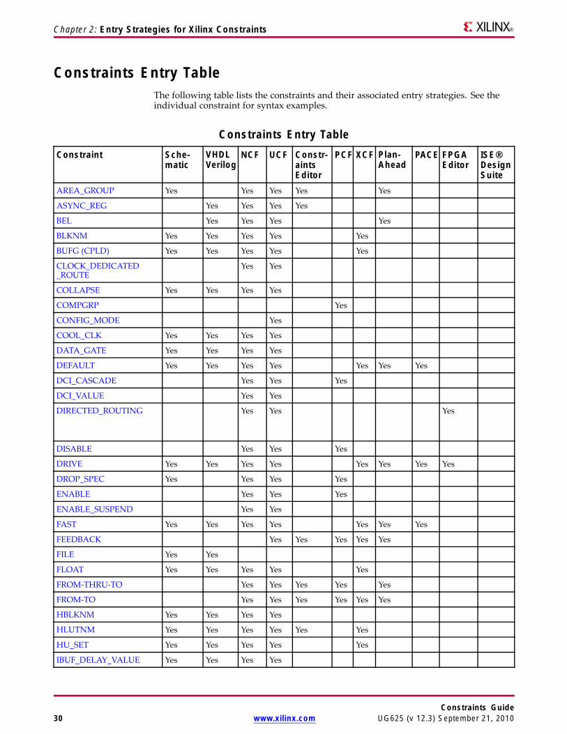
Chapter 2: Entry Strategies for Xilinx Constraints
Constraints Entry TableThe following table lists the constraints and their associated entry strategies. See theindividual constraint for syntax examples.
Constraints Entry TableConstraint Sche-
maticVHDLVerilog
NCF UCF Constr-aintsEditor
PCF XCF Plan-Ahead
PACE FPGAEditor
ISE®DesignSuite
AREA_GROUP Yes Yes Yes Yes Yes
ASYNC_REG Yes Yes Yes Yes
BEL Yes Yes Yes Yes
BLKNM Yes Yes Yes Yes Yes
BUFG (CPLD) Yes Yes Yes Yes Yes
CLOCK_DEDICATED_ROUTE
Yes Yes
COLLAPSE Yes Yes Yes Yes
COMPGRP Yes
CONFIG_MODE Yes
COOL_CLK Yes Yes Yes Yes
DATA_GATE Yes Yes Yes Yes
DEFAULT Yes Yes Yes Yes Yes Yes Yes
DCI_CASCADE Yes Yes Yes
DCI_VALUE Yes Yes
DIRECTED_ROUTING Yes Yes Yes
DISABLE Yes Yes Yes
DRIVE Yes Yes Yes Yes Yes Yes Yes Yes
DROP_SPEC Yes Yes Yes Yes
ENABLE Yes Yes Yes
ENABLE_SUSPEND Yes Yes
FAST Yes Yes Yes Yes Yes Yes Yes
FEEDBACK Yes Yes Yes Yes Yes
FILE Yes Yes
FLOAT Yes Yes Yes Yes Yes
FROM-THRU-TO Yes Yes Yes Yes Yes
FROM-TO Yes Yes Yes Yes Yes Yes
HBLKNM Yes Yes Yes Yes
HLUTNM Yes Yes Yes Yes Yes Yes
HU_SET Yes Yes Yes Yes Yes
IBUF_DELAY_VALUE Yes Yes Yes Yes
Constraints Guide30 www.xilinx.com UG625 (v 12.3) September 21, 2010

Chapter 2: Entry Strategies for Xilinx Constraints
Constraint Sche-matic
VHDLVerilog
NCF UCF Constr-aintsEditor
PCF XCF Plan-Ahead
PACE FPGAEditor
ISE®DesignSuite
IFD_DELAY_VALUE Yes Yes Yes Yes
INREG Yes Yes
IOB Yes Yes Yes Yes Yes Yes
IOBDELAY Yes Yes Yes Yes Yes
IODELAY_GROUP Yes
IOSTANDARD Yes Yes Yes Yes Yes Yes Yes Yes
KEEP Yes Yes Yes Yes Yes
KEEPER Yes Yes Yes Yes Yes Yes Yes
KEEP_HIERARCHY Yes Yes Yes Yes Yes Yes
LOC Yes Yes Yes Yes Yes Yes Yes Yes
LOCATE Yes Yes
LOCK_PINS Yes Yes Yes
LUTNM Yes Yes Yes Yes
MAP Yes Yes Yes
MAXDELAY Yes Yes Yes Yes Yes Yes Yes
MAX_FANOUT Yes Yes Yes
MAXPT Yes Yes Yes
MAXSKEW Yes Yes Yes Yes Yes Yes Yes
NODELAY Yes Yes Yes Yes Yes
IODELAY_GROUP Yes
NOREDUCE Yes Yes Yes Yes Yes
OFFSET IN Yes Yes Yes Yes Yes Yes Yes
OFFSET OUT Yes Yes Yes Yes Yes Yes Yes
OPEN_DRAIN Yes Yes Yes Yes Yes
PERIOD Yes Yes Yes Yes Yes Yes Yes Yes Yes
PIN Yes
POST_CRC Yes Yes
POST_CRC_ACTION Yes Yes
POST_CRC_FREQ Yes Yes
POST_CRC_INIT_FLAG Yes Yes
PRIORITY Yes Yes Yes
PROHIBIT Yes Yes Yes Yes Yes
PULLDOWN Yes Yes Yes Yes Yes Yes Yes Yes
PULLUP Yes Yes Yes Yes Yes Yes Yes Yes
PWR_MODE Yes Yes Yes Yes Yes
REG Yes Yes Yes Yes Yes
Constraints GuideUG625 (v 12.3) September 21, 2010 www.xilinx.com 31

Chapter 2: Entry Strategies for Xilinx Constraints
Constraint Sche-matic
VHDLVerilog
NCF UCF Constr-aintsEditor
PCF XCF Plan-Ahead
PACE FPGAEditor
ISE®DesignSuite
RLOC Yes Yes Yes Yes Yes Yes
RLOC_ORIGIN Yes Yes Yes Yes Yes Yes
RLOC_RANGE Yes Yes Yes Yes Yes Yes
SAVE NET FLAG Yes Yes Yes Yes Yes
SCHMITT_TRIGGER Yes Yes Yes Yes Yes
SLEW Yes Yes Yes Yes Yes Yes Yes Yes
SLOW Yes Yes Yes Yes Yes Yes Yes Yes
STEPPING Yes
SUSPEND Yes Yes Yes Yes Yes
SYSTEM_JITTER Yes Yes Yes Yes Yes
TEMPERATURE Yes Yes Yes Yes
TIG Yes Yes Yes Yes Yes Yes Yes
TIMEGRP Yes Yes Yes Yes Yes Yes
TIMESPEC Yes Yes Yes Yes Yes
TNM Yes Yes Yes Yes Yes
TNM_NET Yes Yes Yes Yes Yes Yes
TPSYNC Yes Yes Yes
TPTHRU Yes Yes Yes Yes
TSidentifier Yes Yes Yes Yes Yes Yes
U_SET Yes Yes Yes Yes Yes
USE_RLOC Yes Yes Yes Yes Yes Yes
VCCAUX Yes Yes
VOLTAGE Yes Yes Yes Yes
VREF Yes Yes Yes
WIREAND Yes Yes Yes Yes
XBLKNM Yes Yes Yes Yes Yes
Schematic DesignFollow these rules to add Xilinx® constraints as attributes within a symbol or schematicdrawing:
• If a constraint applies to a net, add it as an attribute to the net.
• If a constraint applies to an instance, add it as an attribute to the instance.
• You cannot add global constraints such as PART and PROHIBIT.
• You cannot add any timing specifications that would be attached to a TIMESPECor TIMEGRP.
• Enter attribute names and values in either all uppercase or all lowercase. Mixeduppercase and lowercase is not allowed.
Constraints Guide32 www.xilinx.com UG625 (v 12.3) September 21, 2010

Chapter 2: Entry Strategies for Xilinx Constraints
For more information about creating, modifying, and displaying attributes, see theSchematic and Symbol Editors Help.
The syntax for any constraint that can be entered in a schematic is described in thesection for that constraint. For an example of correct schematic syntax, see the SchematicSyntax Example in BEL.
VHDL AttributesIn VHDL code, constraints can be specified with VHDL attributes. Before it can be used,a constraint must be declared with the following syntax:
attribute attribute_name : string;
Example
attribute RLOC : string;
An attribute can be declared in an entity or architecture.
• If the attribute is declared in the entity, it is visible both in the entity and thearchitecture body.
• If the attribute is declared in the architecture, it cannot be used in the entitydeclaration.
Once the attribute is declared, you can specify a VHDL attribute as follows:
attribute attribute_name of {component_name | label_name|entity_name|signal_name |variable_name |type_name}:{component|label| entity|signal |variable |type} is attribute_value ;
Accepted attribute_values depend on the attribute type.
Example One
attribute RLOC : string;
attribute RLOC of u123 : label is "R11C1.S0";
Example Two
attribute bufg: string;
attribute bufg of my_clock: signal is "clk";
For Xilinx® the most common objects are signal, entity, and label. A labeldescribes an instance of a component.
Note The signal attribute must be used on the output port.
VHDL is case insensitive.
In some cases, existing Xilinx constraints cannot be used in attributes, since they are alsoVHDL keywords. To avoid this naming conflict, use a constraint alias. Each Xilinxconstraint has its own alias. The alias is the original constraint name pre-pended withthe prefix XIL_ For example, the RANGE constraint cannot be used in an attributedirectly. Use XIL_RANGE instead.
Verilog AttributesVerilog attributes are bounded by asterisks (*), and use the following syntax:
(* attribute_name = attribute_value *)
Constraints GuideUG625 (v 12.3) September 21, 2010 www.xilinx.com 33

Chapter 2: Entry Strategies for Xilinx Constraints
where• attribute precedes the signal, module, or instance declaration to which it refers.• attribute_value is a string. No integer or scalar values are allowed.• attribute_value is between quotes.• The default is 1. (* attribute_name *) is the same as (* attribute_name =
"1" *).
Verilog Attributes Syntax Example One(* clock_buffer = "IBUFG" *) input CLK;
Verilog Attributes Syntax Example Two(* INIT = "0000" *) reg [3:0] d_out;
Verilog Attributes Syntax Example Threealways@(current_state or reset)begin (* parallel_case *) (* full_case *)case (current_state)
Verilog Attributes Syntax Example Four(* mult_style = "pipe_lut" *) MULT my_mult (a, b, c);
Verilog LimitationsVerilog attributes are not supported for:• Signal declarations• Statements• Port connections• Expression operators
Verilog Meta CommentsConstraints can also be specified in Verilog code using meta comments. The Verilogformat is the preferred syntax, but the meta comment style is still supported. Use thefollowing syntax:
// synthesis attribute AttributeName [of] ObjectName [is] AttributeValue
Verilog Meta Comments Examples// synthesis attribute RLOC of u123 is R11C1.S0// synthesis attribute HU_SET u1 MY_SET// synthesis attribute bufg of my_clock is "clk"
User Constraints File (UCF)A User Constraints File (UCF) file is an ASCII file which specifies constraints on thelogical design. You can create UCF files and enter constraints with:• Any text editor• Constraints Editor
These constraints affect how the logical design is implemented in the target device. Youcan use UCF files to override constraints specified during design entry.
Constraints Guide34 www.xilinx.com UG625 (v 12.3) September 21, 2010

Chapter 2: Entry Strategies for Xilinx Constraints
UCF FlowThe following figure illustrates the UCF flow.
UCF Flow
UCF files are input to NGDBuild (see the preceding figure). The constraints in theUCF files become part of the information in the NGD file produced by NGDBuild.For FPGA devices, some of these constraints are used when the design is mapped byMAP, and some of the constraints are written into the Physical Constraints File (PCF)produced by MAP.
The constraints in the PCF file are used by each of the physical design tools (for example,PAR and the timing analysis tools), which are run after the design is mapped.
Manual Entry of Timing ConstraintsIn addition to entering timing constraints through Constraints Editor, you can manuallyenter timing specifications as constraints in UCF files. When you run NGDBuild on thedesign, the timing constraints are added to the design database as part of the NGD file.You can also use the Constraints Editor to enter timing constraints in UCF files.
Constraint Conflicts in Multiple UCF FilesThe Xilinx® software still uses "last constraint wins" just as in HDL, NCF, UCF, and PCFprocessing. Currently, the UCF files are processed in the order in which they are addedto the project (either in the ISE® Design Suite or by means of Tcl commands), and it hasno bearing on timestamps or the order in which the files were modified.
User Constraints File (UCF) and Netlist Constraints File (NCF)File Syntax
Logical constraints are found in:
• The Netlist Constraints File (NCF), an ASCII file typically generated by synthesisprograms
• The User Constraints File (UCF), an ASCII file generated by the user
Xilinx® recommends that you place user-generated constraints in the UCF or NCF filesand not in the Physical Constraints File (PCF) file.
Constraints GuideUG625 (v 12.3) September 21, 2010 www.xilinx.com 35

Chapter 2: Entry Strategies for Xilinx Constraints
General Rules for UCF and NCF• UCF and NCF files are case sensitive. Identifier names (names of objects, such as
net names) must exactly match the case of the name as it exists in the source designnetlist. However, any Xilinx constraint keyword (for example, LOC, PERIOD,HIGH, LOW) may be entered in all uppercase, all lowercase, or mixed case.
• Each statement is terminated by a semicolon (;).• No continuation characters are necessary if a statement exceeds one line, since a
semicolon marks the end of the statement.• Xilinx recommends that you group similar blocks, or components, as a single timing
constraint, and not as separate timing constraints.• To add comments to the UCF and NCF files, begin each comment line with a pound
(#) sign, as in the following example.
# file TEST.UCF# net constraints for TEST designNET "$SIG_0 MAXDELAY" = 10;NET "$SIG_1 MAXDELAY" = 12 ns;
• Statements need not be placed in any particular order in the UCF and NCF file.• Enclose NET and INST names in double quotes (recommended but not mandatory).• Enclose inverted signal names that contain a tilde (for example, ~OUTSIG1) in
double quotes (mandatory).• You can enter multiple constraints for a given instance. For more information, see
Entering Multiple Constraints below.
Conflict in ConstraintsThe constraints in the UCF and NCF files and the constraints in the schematic orsynthesis file are applied equally. It does not matter whether a constraint is entered inthe schematic, HDL, UCF or NCF files. If the constraints overlap, UCF overrides NCFand schematic/netlist constraints. NCF overrides schematic/netlist constraints.
If by mistake two or more elements are locked onto a single location, MAP detectsthe conflict, issues an error message, and stops processing so that you can correct themistake.
SyntaxThe UCF file supports a basic syntax that can be expressed as:
{NET|INST|PIN} "full_name" constraint;• full_name is a full hierarchically qualified name of the object being referred to. When
the name refers to a pin, the instance name of the element is also required.• constraint is a constraint in the same form as it would be used if it were attached as
an attribute on a schematic object. For example, LOC=P38 and FAST.
Specifying Attributes for TIMEGRP and TIMESPECTo specify attributes for TIMEGRP, the keyword TIMEGRP precedes the attributedefinitions in the constraints files.
TIMEGRP "input_pads"=PADS EXCEPT output_pads;
Constraints Guide36 www.xilinx.com UG625 (v 12.3) September 21, 2010

Chapter 2: Entry Strategies for Xilinx Constraints
Using Reserved WordsIn all of the constraints files (NCF, UCF, and PCF), instance or variable names that matchinternal reserved words may be rejected unless the names are enclosed in double quotes.It is good practice to enclose all names in double quotes.
For example, the following entry is not accepted because the word net is a reserved word.
NET "net" OFFSET=IN 20 BEFORE CLOCK;
Following is the recommended way to enter the constraint.
NET "net" OFFSET=IN 20 BEFORE CLOCK;
or
NET "$SIG_0" OFFSET=IN 20 BEFORE CLOCK;
Enclose inverted signal names that contain a tilde (for example, ~OUTSIG1) in doublequotes (mandatory) as follows:
NET "~OUTSIG1" OFFSET=IN 20 BEFORE CLOCK;
WildcardsYou can use the wildcard characters, asterisk (*) and question mark (?) in constraintstatements as follows:• The asterisk (*) represents any string of zero or more characters.• The question mark (?) indicates a single character.
In net names, the wildcard characters enable you to select a group of symbols whoseoutput net names match a specific string or pattern. For example, the constraint shownbelow increases the output speed of pads to which nets are connected with names thatmeet the following patterns:• They begin with any series of characters (represented by an asterisk [*]).• The initial characters are followed by "AT."• The net names end with one single character (represented by a question mark [?].
NET "*AT?" FAST;
In an instance name, a wildcard character by itself represents every symbol of theappropriate type. For example, the following constraint initializes an entire set of ROMsto a particular hexadecimal value, 5555.
INST "$1I3*/ROM2" INIT=5555;
If the wildcard character is used as part of a longer instance name, the wildcardrepresents one or more characters at that position.
In a location, you can use a wildcard character for either the row number or the columnnumber. For example, the following constraint specifies placement of any instance underthe hierarchy of loads_of_logic in any SLICE in column 8.
INST "/loads_of_logic/*" LOC=SLICE_X*Y8;
Wildcard characters cannot be used for both the row number and the column number ina single constraint, since such a constraint is meaningless.
Traversing HierarchiesTop-level block names (design names) are ignored when searching for instance namematches. You can use the asterisk wildcard character (*) to traverse the hierarchy of adesign within a UCF and NCF file. The following syntax applies (where level1 is anexample hierarchy level name).
Constraints GuideUG625 (v 12.3) September 21, 2010 www.xilinx.com 37

Chapter 2: Entry Strategies for Xilinx Constraints
UCF Design Hierarchy* Traverses all levels of the hierarchy
level1/* Traverses all blocks in level1 and below
level1/*/ Traverses all blocks in the level1 hierarchylevel but no further
Consider the following design hierarchy.
UCF Design Hierarchy
With the example design hierarchy, the following specifications illustrate the scope ofthe wildcard.
INST * => <everything>INST /* => <everything>INST /*/ => <$A1,$B1,$C1>INST $A1/* => <$A21,$A22,$A3,$A4>INST $A1/*/ => <$A21,$A22>INST $A1/*/* => <$A3,$A4>INST $A1/*/*/ => <$A3>INST $A1/*/*/* => <$A4>INST $A1/*/*/*/ => <$A4>INST /*/*22/ => <$A22,$B22,$C22>INST /*/*22 => <$A22,$A3,$A4,$B22,$B3,$C3>
Entering Multiple ConstraintsYou can cascade multiple constraints for a given instance in the UCF file:
INST instanceName constraintName = constraintValue | constraintName = constraintValue;
For example:
INST myInst LOC = P53 | IOSTANDARD = LVPECL33 | SLEW = FAST;
File NameBy default, NGDBuild reads the constraints file that carries the same name as the inputdesign with a .ucf extension. However, you can specify a different constraints file namewith the -uc option when running NGDBuild. NGDBuild automatically reads in theNCF file if it has the same base name as the input EDIF file and is in the same directoryas the EDIF file.
The implementation tools (for example, NGDBuild, MAP, and PAR) require file nameextensions in all lowercase (for example, .ucf) in command lines.
Constraints Guide38 www.xilinx.com UG625 (v 12.3) September 21, 2010
Chapter 2: Entry Strategies for Xilinx Constraints
Instances and BlocksThe statements in the constraints file concern instances and blocks, which are definedas follows.• An instance is a symbol on the schematic.• An instance name is the symbol name as it appears in the EDIF netlist.• A block is a CLB or an IOB.• Specify the block name with the BLKNM, HBLKNM, or XBLKNM attributes. By
default, the software assigns a block name on the basis of a signal name associatedwith the block.
Physical Constraints File (PCF)The Native Generic Database (NGD) file produced when a design netlist is read intothe Xilinx® ISE® Design Suite may contain a number of logical constraints. Theseconstraints originate in any of these sources.• An attribute assigned within a schematic or Hardware Description Language (HDL)
file• A constraint entered in a User Constraints File (UCF)• A constraint appearing in an Netlist Constraints File (NCF) produced by a CAE
vendor toolset
Logical constraints in the NGD file are read by MAP. MAP uses some of the constraintsto map the design and converts logical constraints to physical constraints. MAP thenwrites these physical constraints into a Physical Constraints File (PCF).
The PCF file is an ASCII file containing two separate sections:• A section for those physical constraints created by the mapper• A section for physical constraints entered by the user
The mapper section is rewritten every time you run the mapper.
Mapper-generated physical constraints appear first in the file, followed by user physicalconstraints. In the event of conflicts between mapper-generated and user constraints,user constraints are read last, and override mapper-generated constraints.
The beginning of the mapper-generated section is indicated by SCHEMATIC START. Theend of this section is indicated by SCHEMATIC END. Enter user-generated constraints,such as timing constraints, after SCHEMATIC END.
You can write user constraints directly into the file, or you can write them indirectly (orundo them) from within the FPGA Editor. For more information on constraints in theFPGA Editor, see the FPGA Editor help.
Note Whenever possible, you should add design constraints to the HDL, schematic, orUCF, instead of PCF. This simplifies design archiving and improves design role checking.
The PCF file is an optional input to PAR, FPGA Editor, TRACE, NetGen, and BitGen.
The file may contain any number of constraints, and any number of comments, in anyorder. A comment consists of either a pound sign (#) or double slashes (//) followed byany number of other characters up to a new line. Each comment line must begin witha pound sign (#) or double slashes (//).
The structure of the PCF file is as follows.
schematic start;
translated schematic and UCF and NCF constraints in PCF format
schematic end;
Constraints GuideUG625 (v 12.3) September 21, 2010 www.xilinx.com 39

Chapter 2: Entry Strategies for Xilinx Constraints
user-entered physical constraints
Caution! Put all user-entered physical constraints after the schematic end statement.Any constraints preceding this section or within this section may be overwritten or ignored.
Do not edit the schematic constraints. They are overwritten every time the mappergenerates a new PCF file.
Global constraints need not be attached to any object, but should be entered in aconstraints file.
Indicate the end of each constraint statement with a semicolon.
In all of the constraints files (NCF, UCF, and PCF), instance or variable names that matchinternal reserved words are rejected unless the names are enclosed in double quotes. Itis good practice to enclose all names in double quotes. For example, the following entrywould not be accepted because the word net is a reserved word.
NET net FAST;
Following is the recommended way to enter the constraint.
NET "net" FAST;
Netlist Constraints File (NCF)The syntax rules for the Netlist Constraints File (NCF) are the same as those for the UserConstraints File (UCF). For more information, see User Constraints File (UCF) andNetlist Constraints File (NCF) File Syntax.
Constraints EditorThe Constraints Editor is a graphical tool that simplifies the process of entering timingconstraints. This tool guides you through the process of creating constraints withoutrequiring you to understand User Constraints File (UCF) syntax. For the constraints anddevices with which Constraints Editor can be used, see Constraints Entry Methods. Forinformation on running Constraints Editor, see the ISE® Design Suite Help
Constraints Editor is used in the implementation phase after the translation step(NGCBuild). Constraints Editor allows you to create and manipulate constraintswithout any direct editing of the UCF. After the constraints are created or modified withConstraints Editor, NGCBuild must be run again, using the new UCF and design sourcenetlist files as input and generating a new NGD file as output.
Input/OutputConstraints Editor requires:
• A User Constraints File (UCF)
• A Native Generic Database (NGD) file
Constraints Editor uses the NGD file to provide names of logical elements for grouping.As output, it uses the UCF file.
After you open Constraints Editor, you must first open a UCF file. If the UCF and NGDroot names are not the same, you must select the appropriate NGD file to open. Formore information, see the Constraints Editor Help.
Constraints Guide40 www.xilinx.com UG625 (v 12.3) September 21, 2010

Chapter 2: Entry Strategies for Xilinx Constraints
Upon successful completion, Constraints Editor writes out a UCF file. NGCBuild(translation) uses the UCF file, along with design source netlists, to produce an NGDfile. The NGD file is read by the MAP program. MAP generates a physical designdatabase in the form of an Native Circuit Description (NCD) file and also generatesa Physical Constraints File (PCF). The implementation software uses these files toultimately produce a bitstream.
Note Not all Xilinx® constraints are accessible through Constraints Editor.
Starting Constraints EditorConstraints Editor runs on personal computers and workstations. You can startConstraints Editor:• From ISE Design Suite• As a Standalone Tool• From the Command Line
Running Constraints Editor From ISE Design SuiteWithin ISE Design Suite, launch Constraints Editor from the Processes window.1. Select a design file in the Sources window.2. Double-click Processes > Design Utilities > User Constraints > Create Timing
Constraints.
Running Constraints Editor As a Standalone ToolIf you installed Constraints Editor as a standalone tool, either:• Click the Constraints Editor icon on the Windows desktop, or• Select Start > Programs > Xilinx ISE > Accessories> Constraints Editor
Running Constraints Editor From the Command Line With No DataLoaded
To start Constraints Editor from the command line with no data loaded, type:
constraints_editor
Running Constraints Editor From the Command Line With the NGDFile Loaded
To start Constraints Editor from the command line with the NGD file loaded, enter:
constraints_editor ngdfile_namengdfile_name is the name of the NGD file
It is necessary to use the .ngd extension.
If a UCF file with the same base name as the NGD file exists, it is loaded also. Otherwise,you are prompted for a UCF file.
Running Constraints Editor From the Command Line With the NGDFile and the UCF File Loaded
To start Constraints Editor from the command line with the NGD file and the UCFfile loaded, enter:
Constraints GuideUG625 (v 12.3) September 21, 2010 www.xilinx.com 41

Chapter 2: Entry Strategies for Xilinx Constraints
constraints_editor ngdfile_name -uc ucf_file_name• ngdfile_name is the name of the NGD file• ucf_file_name is the name of the UCF file
It is necessary to use the .ucf extension.
Running Constraints Editor From the Command Line As aBackground Process
To run Constraints Editor as a background process on a workstation, enter:
constraints_editor &
ISE Design SuiteTo set implementation constraints in ISE® Design Suite:• For FPGA devices, the implementation process properties specify how a design is
translated, mapped, placed, and routed. You can set multiple properties to controlthe implementation processes.
• For CPLD devices, the implementation process properties specify how a design istranslated and fit.
For more information, see the ISE Design Suite help for the Process Properties dialog box.
PlanAheadYou can use the PlanAhead™ software either before or after synthesis. The PlanAheadsoftware supports the following devices:• Virtex®-4 devices and higher• Spartan®-3 devices and higher
The PlanAhead software allows you to drag-and-drop placement constraints, including:• Pinout• Logic placement• Area
For more information, see the PlanAhead User Guide.
Assigning Placement ConstraintsFor FPGA devices, you can use the PlanAhead software to enter placement constraintsthat control:• I/O pin and logic assignments• Global logic placement• Area group assignment
The PlanAhead software runs automatically at various stages of the design processto allow you to analyze the design and to apply placement constraints. A simplifiedversion of the PlanAhead software is invoked from ISE® Design Suite to enable onlythe types of features required to perform the selected tasks. The standalone PlanAheadsoftware has many more features available.
Constraints Guide42 www.xilinx.com UG625 (v 12.3) September 21, 2010

Chapter 2: Entry Strategies for Xilinx Constraints
When the PlanAhead software is invoked from ISE Design Suite, it is a separate CPUprocess and does not communicate realtime with ISE Design Suite as some other toolsdo. In order to prevent data mismatch or out of sync issues, do not update ISE DesignSuite source files while the PlanAhead software is running .
When the PlanAhead software is invoked, the appropriate source files are passed to thePlanAhead software to populate the PlanAhead Project. When the PlanAhead Project issaved, only the modified UCF files are passed back to ISE Design Suite to update theProject. These input source files vary depending on the process step invoked.
For more information on the types of files passed, see the Pin Assignment andFloorplanning and Placement Constraints sections later in this chapter. The followingsections cover strategies for entering placement constraints using the PlanAheadsoftware.
Defining I/O Pin ConfigurationsThis section discusses Defining I/O Pin Configurations and includes:
• Pin Assignment Overview
• Reviewing I/O Pin Data Information
• Pin Assignment
• I/O Planner Documentation
Pin Assignment OverviewI/O Planner can be invoked either as a standalone tool or from within ISE Design Suite.Invoking I/O Planner standalone can be helpful early in the design process when HDLsources may not yet be complete. I/O ports can be defined manually within the tool,or by importing a CSV format spreadsheet or HDL sources. You can define an initialpinout and export a User Constraints File (UCF) file for use in the ISE Design Suite flow.
A UCF file is required when invoking I/O Planner from within ISE Design Suite. If aUCF file does not exist, an empty one is created. Creation of I/O ports manually orby importing a CSV spreadsheet is not enabled when invoking I/O Planner from ISEDesign Suite.
I/O Planner is an I/O pin assignment environment containing many helpful views andcapabilities. You can selectively drag and drop groups of I/O ports onto the device usinga variety of methods. An automatic placement routine is also available. ComprehensiveDesign Rule Checks (DRCs) ensure legal pinout definition.
Reviewing I/O Pin Data InformationData Sheets provide device specifications, including I/O standards. To get device-specificI/O standard information, see the data sheet for the device you are targeting. A lot ofthe data contained in the data sheets is also available inside of the I/O Planner tool. Thetypes of information available include I/O standards, clock capable pins, internal tracedelays, differential pairs, clock region and I/O bank contents, etc. Information aboutI/O related device resources such as global and regional clock buffers, I/O delays anddelay controllers, gigabit transceivers, etc. is also available.
Constraints GuideUG625 (v 12.3) September 21, 2010 www.xilinx.com 43

Chapter 2: Entry Strategies for Xilinx Constraints
Pin AssignmentTo invoke I/O Planner standalone either click the PlanAhead Windows Desktop iconor enter PlanAhead on the Linux command line. From ISE Design Suite, you can useany of the following methods to start your pin assignment process, which allows you tochoose the method most convenient for you:
• Floorplanning I/O – Pre-Synthesis
When using this command or process step, the HDL source files are passed to thePlanAhead software in order to extract the top level I/O port information only. If aUCF files exists in the ISE Design Suite project, it is passed to the PlanAhead softwarefor modification. If a UCF does not exist, you are prompted to create one. If multipleUCF files exist, you are prompted to select the desired file to add new constraints to.Existing constraints are modified in whichever file they are contained in.
Refer to the I/O Planner Documentation section for information on using the I/OPlanner environment contained in the PlanAhead software.
Once the I/O pin assignment is made, you save the PlanAhead software project andexit the PlanAhead software. This updates the UCF files in the ISE Design Suiteproject and update the project status accordingly. Exiting the PlanAhead softwarewithout saving does not change the ISE Design Suite UCF source files or status.
• Floorplanning a Design – Post-Synthesis
When using this command or process step, the synthesized netlist source files arepassed to the PlanAhead software. If a UCF files exists in the ISE Design Suiteproject, it is passed to the PlanAhead software for modification. If a UCF does notexist, you are prompted to create one. If multiple UCF files exist, you are promptedto select the desired file to add new constraints to. Existing constraints are modifiedin whichever file they are contained in.
Having a synthesized netlist as input enables more functionality in I/O Planner sincethe tool is now aware of the clocks and clock related logic in the design. AdditionalI/O planning capabilities and DRCs are provided to make more intelligent pinassignment decisions. The design connectivity can also be analyzed to ensureoptimized use of device resources in relation to the I/Os.
Refer to the I/O Planner Documentation section for information on using the I/OPlanner environment contained in the PlanAhead software.
Once the I/O pin assignment is made, you will then save the PlanAhead softwareproject and exit the PlanAhead software. This will update the UCF files in the ProjectNavigator project and update the project status accordingly. Exiting PlanAheadwithout saving with not change the ISE Design Suite UCF source files or status.
I/O Planner DocumentationThe PlanAhead User Guide contains a section on I/O Pin Planning with I/O Planner thatprovides information on using I/O Planner for analyzing the device resources and I/Opin assignment.
The PlanAhead Tutorial contains a section on I/O Pin Assignment with I/O Planner for tohelp you quickly get up to speed with I/O Planner.
A I/O Planner video demonstration is also available at www.xilinx.com/design.
Constraints Guide44 www.xilinx.com UG625 (v 12.3) September 21, 2010
Chapter 2: Entry Strategies for Xilinx Constraints
Floorplanning and Placement ConstraintsThe PlanAhead software provides a comprehensive environment for analyzing thedesign from a number of different aspects including connectivity, density, and timing.You can then apply placement constraints to help drive the implementation tools towardbetter or more consistent results. These constraints may include LOC constraints to lockspecific logic objects into specific sites on the device or AREA_GROUP constraints toconstrain a group of logic within a specific area of the device.
For more information on the types of placement constraints available, see ConstraintsOverview.
Placement LOC Constraint AssignmentThe PlanAhead software enables you to lock down any logic to specific device sites. Thisoften includes global logic objects such as the following: BUFG, BRAM, MULT, PPC405,GT, DLL, and DCM.
You can place logic objects by simply dragging the desired logic object from any of theappropriate PlanAhead software views and drop it in the Device View in the Workspace.Some types of logic such as I/O ports enable you to enter the desired location site in theobject General Properties view.
For more information about assigning placement constraints, see the Floorplanning theDesign -> Using Placement Constraints section of the PlanAhead User Guide.
Area Group AssignmentArea groups are the primary means of placing logic in specific regions of the device, forexample, within a particular clock region. The PlanAhead software enables you to createarea groups using a wide variety of methods. Assistance with connectivity, size logictypes and ranges are all provided by the tool including DRCs to ensure proper AreaGroup (AREA_GROUP) property definition.
For more information about creating area group constraints, see Floorplanning the Designin the PlanAhead User Guide.
Setting Constraints in the Pinout & Area Constraints Editor(PACE)
For CPLD devices, you can set constraints in the Pinout & Area Constraints Editor(PACE). The Pin Assignments Editor in PACE is used mainly to assign locationconstraints to IOs. It is also used to assign IO properties such as IO Standards.
For a list of the constraints and devices with which PACE can be used, see ConstraintsEntry Methods. For more information about accessing and using PACE, see the ISE®Design Suite Help.
Partial Design Pin PreassignmentThis section deals with Pin Preassignment when a design is partially completed. Forinformation on Pin Preassignment in which a Hardware Description Language (HDL)template is built by adding constraints to pins that are defined within PlanAhead™or PACE, see the ISE® Design Suite Help. PACE is supported for CPLD devices.PlanAhead is supported for FPGA devices.
Constraints GuideUG625 (v 12.3) September 21, 2010 www.xilinx.com 45

Chapter 2: Entry Strategies for Xilinx Constraints
Designs that are not yet fully coded might still have layout requirements. Pinassignments, voltage standards, banking rules, and other board requirements might bein place long before the design has reached the point where these constraints can beapplied. Pin Preassignment allows the design pinout rules to be determined before thedesign logic has been completed.
To use Pin Preassignment in PlanAhead or PACE:
1. Provide the complete list of ports in your top-level design
2. Assign I/O constraints to them
Even if the ports are not used by any logic (that is, no loads for input pins, no sources foroutput pins), they can still receive constraints and be kept through implementation.
Assign Location (LOC) or Input Output Standard (IOSTANDARD) constraints in theUser Constraints File (UCF) just like for any I/O pin. These requirements are annotatedin the database. PlanAhead and PACE can be used to assign pin locations, bankinggroups or voltage standards, and DRC checks can be run. The final PAD report containsany pins that have logic or constraints associated with them.
This implementation is incomplete and cannot be downloaded to the hardware. Youshould expect these errors during the DRC phase of bitstream generation (BitGen):
• ERROR: PhysDesignRules:368 - The signal <D_OBUF> is incomplete. The signal isnot driven by any source pin in the design.
• ERROR: PhysDesignRules:10 - The network <D_OBUF> is completely unrouted.
To trim any unused ports from the design, remove the associated constraints. TheTranslate (NGDBuild) phase trims these unused pins.
In this example, there are six top-level ports. Only three (clk, A, C) are currently used.Of the remaining three ports:
• B is kept because it has a Location (LOC) constraint.
• D is kept because it has an Input Output Standard (IOSTANDARD) constraint.
• E is trimmed because it is completely unused and unconstrained.
Verilog Example--------------module design_top(clk, A, B, C, D, E);input clk, A, B;output reg C, D, E;
always@(posedge clk)C <= A;
endmodule
UCF Example--------
NET "A" LOC = "E2" ;NET "B" LOC = "E3" ;NET "C" LOC = "B15" ;NET "D" IOSTANDARD = SSTL2_II ;
Constraints Guide46 www.xilinx.com UG625 (v 12.3) September 21, 2010

Chapter 2: Entry Strategies for Xilinx Constraints
FPGA EditorYou can add or delete certain constraints in the Physical Constraints File (PCF) usingFPGA Editor. FPGA Editor supports net, site, and component constraints as propertyfields in the individual nets and components. Properties are set with the Setattrcommand, and are read with the Getattr command.
All Boolean constraints, including BLOCK, Locate (LOCATE), LOCK, Offset In (OFFSETIN), Offset Out (OFFSET OUT), and Prohibit (PROHIBIT), have values of On or Off.Offset direction has a value of either In or Out. Offset order has a value of eitherBefore or After. All other constraints have a numeric value. They can also be set toOff in order to delete the constraint. All values are case-insensitive (for example, Onand on are both accepted).
When you create a constraint in the FPGA Editor, the constraint is written to the PCF filewhenever you save your design. When you use the FPGA Editor to delete a constraint,and then save your design file, the line on which the constraint appears in the PCFfile remains in the file but is automatically commented out. Some of the constraintssupported in the FPGA Editor are listed in the following table.
Constraints Supported in FPGA EditorConstraint Accessed Throughblock paths Component Properties and Path Properties
property sheet
define path Viewed with Path Properties property sheet
location range Component Properties Constraints page
locate macro Macro Properties Constraints page
lock placement Component Properties Constraints page
lock routing of this net Net Properties Constraints page
lock routing Net Properties Constraints page
maxdelay allnets Main Properties Constraints page
maxdelay allpaths Main Properties Constraints page
maxdelay net Net Properties Constraints page
maxdelay path Path Properties property sheet
maxskew Main Properties Constraints page
maxskew net Net Properties Constraints page
offset comp Component Properties Offset page
penalize tilde Main Properties Constraints page
period Main Properties Constraints page
period net Net Properties Constraints page
prioritize net Net Properties Constraints page
prohibit site Site Properties property sheet
Locked Nets and ComponentsIf a net is locked, you cannot unroute any portion of the net, including the entire net, anet segment, a pin, or a wire. To unroute the net, you must first unlock it. You can addpins or routing to a locked net.
Constraints GuideUG625 (v 12.3) September 21, 2010 www.xilinx.com 47

Chapter 2: Entry Strategies for Xilinx Constraints
A net is displayed as locked in the FPGA Editor if the Lock Net [ net_name] constraintis enabled in the PCF file. You can use the Net Properties property sheet to removethe lock constraint.
When a component is locked, one of the following constraints is set in the PCF file.
lock comp [comp_name]
locate comp [comp_name]
lock macro [macro_name]
lock placement
If a component is locked, you cannot unplace it, but you can unroute it. To unplacethe component, you must first unlock it.
Interaction Between ConstraintsSchematic constraints are placed at the beginning of the PCF file by MAP. The start ofthis section is indicated with SCHEMATIC START. The end of this section is indicatedwith SCHEMATIC END. Because of a last-read order, all constraints that you enter in thisfile should come after SCHEMATIC END.
You are not prohibited from entering a user constraint before the schematic constraintssection, but if you do, a conflicting constraint in the schematic-based section mayoverride your entry.
Every time a design is remapped, the schematic section of the PCF file is overwrittenby the mapper. The user constraints section is left intact, but certain constraints maybe invalid because of the new mapping.
XST Constraint File (XCF)XST constraints can be specified in the XST Constraint File (XCF). The XCF has anextension of .xcf. For more information, see:
• ISE® Design Suite Help
• XST Constraint File (XCF) section in the XST User Guide
Constraints PriorityIn some cases more than one timing constraint covers the same path. The constraintconflict must be resolved, with the higher priority constraint taking precedence andbeing applied to the path, and the lower priority constraints being ignored for thatpath. The method of constraints resolution depends on both the order of constraintspecification as well as the priority of the constraints specified. The rules of constraintpriority resolution are described below. This determination is based upon the constraintprioritization or which constraint appears later in the Physical Constraints File (PCF), ifthere are overlapping constraints of the same priority. For example, if the design hastwo Period (PERIOD) constraints that cover the same paths, the later Period (PERIOD)constraint in the PCF file covers or analyzes these paths. The previous Period (PERIOD)constraints have “0 items analyzed” in the timing report. In order to modify thedefault constraint resolution behavior, the constraint priority can be assigned usingthe PRIORITY keyword.
Constraints Guide48 www.xilinx.com UG625 (v 12.3) September 21, 2010

Chapter 2: Entry Strategies for Xilinx Constraints
File PrioritiesWhen conflicting constraints have the same priority, the order of specification is used todetermine the constraint that takes precedence. The resolution rule for identical priorityconstraints is the constraint that is specified last overwrites any previously definedconstraints. This rule applies to constraints within a single User Constraints File (UCF)as well as constraints defined in multiple UCF files.
The following list defines the precedence order of identical priority constraints whenthese constraints are defined in different constraint files. The list is given in descendingpriority order with the highest priority constraint listed first.• Constraints in a Physical Constraints File (PCF)• Constraints in a User Constraints File (UCF)• Constraints in a Netlist Constraints File (NCF)• Attributes in a schematic or Constraints specified in HDL that are passed down
in the netlist
Timing Specification PrioritiesWhen two different constraints cover the same path, the constraint with the highestpriority takes precedence and is applied to that path. Other constraints are ignored.Constraints priority is as follows, in descending order from highest to lowest.• Timing Ignore (TIG)• From Thru To (FROM-THRU-TO)
– Source and Destination are User Defined Groups– Source or Destination are User Defined Groups– Source and Destination are Predefined Groups
• From To (FROM-TO)– Source and Destination are User Defined Groups– Source or Destination are User Defined Groups– Source and Destination are Predefined Groups
• OFFSET IN (Offset In) and OFFSET OUT (Offset Out)– Specific Data IOB (NET OFFSET) Constraint– Time Group of Data IOBs (Grouped OFFSET) Constraint– All Data IOBs (Global OFFSET) Constraint
• Period (PERIOD)
OFFSET PrioritiesIf two specific OFFSET constraints at the same level of precedence cover the samepath, an OFFSET with a register qualifier takes precedence over an OFFSET without aqualifier; if otherwise equivalent, the latter in the constraint file takes precedence.
MAXSKEW and MAXDELAY PrioritiesNet delay and net skew specifications are analyzed independently of path delay analysisand do not interfere with one another. NET TIG do interact with the NET constraintsand take precedence.
Constraints GuideUG625 (v 12.3) September 21, 2010 www.xilinx.com 49
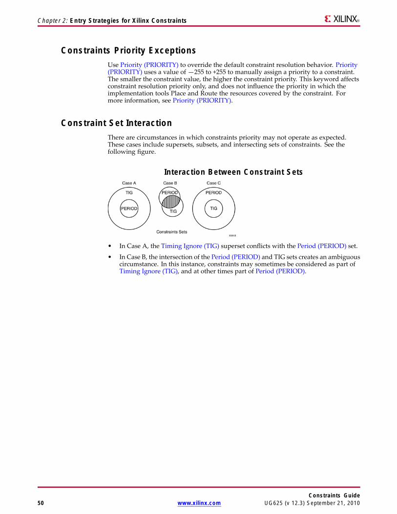
Chapter 2: Entry Strategies for Xilinx Constraints
Constraints Priority ExceptionsUse Priority (PRIORITY) to override the default constraint resolution behavior. Priority(PRIORITY) uses a value of —255 to +255 to manually assign a priority to a constraint.The smaller the constraint value, the higher the constraint priority. This keyword affectsconstraint resolution priority only, and does not influence the priority in which theimplementation tools Place and Route the resources covered by the constraint. Formore information, see Priority (PRIORITY).
Constraint Set InteractionThere are circumstances in which constraints priority may not operate as expected.These cases include supersets, subsets, and intersecting sets of constraints. See thefollowing figure.
Interaction Between Constraint Sets
• In Case A, the Timing Ignore (TIG) superset conflicts with the Period (PERIOD) set.
• In Case B, the intersection of the Period (PERIOD) and TIG sets creates an ambiguouscircumstance. In this instance, constraints may sometimes be considered as part ofTiming Ignore (TIG), and at other times part of Period (PERIOD).
Constraints Guide50 www.xilinx.com UG625 (v 12.3) September 21, 2010

Chapter 3
Timing Constraint StrategiesThe goal of using timing constraints is to ensure that all the design requirements arecommunicated to the implementation tools. This goal also implies that all paths arecovered by the appropriate constraint. This chapter provides general guidelines thatexplain the strategy for identifying and constraining the most common timing paths inFPGA devices in the most efficient manner possible. This chapter contains the followingsections:
• Basic Constraints Methodology
• Input Timing Constraints
• Register-to-Register Timing Constraints
• Output Timing Constraints
• Exception Timing Constraints
Note For more information, see the Timing Constraints User Guide.
Basic Constraints MethodologyIn order to ensure a valid design, the timing requirements for all paths must becommunicated to the implementation software. The timing requirements can be brokendown into several global categories based on the type of path that is to be covered. Themost common types of path categories include:
• Input paths
• Register-to-register paths
• Output paths
• Path specific exceptions
A Xilinx® timing constraint is associated with each of these global category types. Themost efficient way to specify these constraints is to begin with global constraints, thenadd path specific exceptions as needed. In many cases, only the global constraints arerequired.
The FPGA implementation software is driven by the specified timing requirements.The software assigns device resources, and expends the appropriate amount of effortnecessary to ensure that the timing requirements are met. However, when a requirementis over-constrained (or specified as a value greater than the design requirement), theeffort to meet this constraint increases significantly, and results in increased memoryuse and tool runtime. In addition, over-constraining can degrade performance for notonly that particular constraint, but for other constraints as well. For this reason, Xilinxrecommends that you specify the constraint values using the actual design requirements.
Constraints GuideUG625 (v 12.3) September 21, 2010 www.xilinx.com 51

Chapter 3: Timing Constraint Strategies
The method of applying constraints given in this guide uses User Constraints File (UCF)constraint syntax examples. This format highlights the constraints syntax that conveysthe design requirements. However, the easiest way to enter design constraints is touse Constraints Editor, which:
• Provides a unified location in which to manage all timing constraints associatedwith a design
• Provides assistance in creating timing constraints from the design requirements
Input Timing ConstraintsThis section discusses how to specify input timing constraints and includes:
• Input Timing Constraints Overview
• System Synchronous Input
• Timing Diagram for Ideal System Synchronous SDR Interface Example
• Source Synchronous Inputs
• Timing Diagram for Ideal Source Synchronous DDR Interface Example
Input Timing Constraints OverviewInput timing constraints cover the data path from the external pin of the FPGA device tothe internal register that captures that data. Use OFFSET IN to specify the input timing.The best way to specify the input timing requirements depends on the type (source orsystem synchronous) and data rate (SDR or DDR) of the interface.
OFFSET IN defines the relationship between the data and the clock edge used to capturethat data at the pins of the FPGA device. When analyzing OFFSET IN, the timinganalysis software automatically take all internal factors affecting the delay of the clockand data into account. These factors include:
• Frequency and phase transformations of the clock
• Clock uncertainties
• Data delay adjustments
In addition to the automatic adjustments, you may also add additional input clockuncertainty to the PERIOD constraint associated with the interface clock. For moreinformation on the PERIOD constraint and adding INPUT_JITTER, see PERIOD.
OFFSET IN is associated with a single input clock. By default, OFFSET IN covers allpaths from the input pads of the FPGA device to the internal registers that capture thatdata and are triggered by the specified OFFSET IN clock. This application of OFFSET INis called the global method, and is the most efficient way to specify input timing.
System Synchronous InputsThe system synchronous interface is an interface in which a common system clock isused to both transfer and capture the data. The following figure shows a simplifiedSystem Synchronous interface with associated SDR timing.
Constraints Guide52 www.xilinx.com UG625 (v 12.3) September 21, 2010

Chapter 3: Timing Constraint Strategies
Because this interface uses a common system clock, board trace delays and skew limitthe operating frequency of the interface. The lower frequency also results in the systemsynchronous input interface typically being a single data rate (SDR) application. Inthis system synchronous SDR application example, the data is transmitted from thesource device on one rising clock edge and captured in the FPGA device on the nextrising clock edge.
Using OFFSET IN is the most efficient way to specify the input timing for a systemsynchronous interface. In this method, one PERIOD constraint is defined for eachsystem synchronous input interface clock. This single constraint covers the paths of allinput data bits that are captured in registers triggered by the specified input clock.
To specify the input timing:1. Specify the clock OFFSET IN constraint for the input clock associated with the
interface.2. Define the global OFFSET IN constraint for the interface.
Timing Diagram for Ideal System Synchronous SDR Interface ExampleThe following example shows a timing diagram for an ideal System Synchronous SDRinterface. The interface has a clock period of 5 ns and the data for both bits of the busremains valid for the entire period.
The global OFFSET IN constraint is defined as:
OFFSET = IN value VALID value BEFORE clock;
Constraints GuideUG625 (v 12.3) September 21, 2010 www.xilinx.com 53

Chapter 3: Timing Constraint Strategies
For OFFSET IN, value determines the time from the capturing clock edge in which datafirst becomes valid. In this system synchronous example, the data becomes valid 5ns before the capturing clock edge. For OFFSET IN, the VALID value determines theduration in which data remains valid. In this example, the data remains valid for 5 ns.For this example, the complete OFFSET IN specification with an associated PERIOD is:
NET “SysCLk” TNM_NET = “SysClk”;
TIMESPEC “TS_SysClk” = PERIOD “SysClk” 5 ns HIGH 50%;
OFFSET = IN 5 ns VALID 5 ns BEFORE “SysClk”;
This global constraint covers both data bits of the bus (data1, data2).
Source Synchronous InputsThe source synchronous interface is an interface in which a clock is regenerated andtransmitted along with the data from the source device. This clock is then used tocapture the data in the FPGA device. A simplified Source Synchronous interface withassociated DDR timing is shown in the following diagram.
Because this interface uses a regenerated clock that is transmitted along the same boardtraces as the data, the board trace delays and skew no longer limit the operatingfrequency of the interface. The higher frequency also results in the source synchronousinput interface typically being a dual data rate (DDR) application. In this sourcesynchronous DDR application example, unique data is transmitted from the sourcedevice on both the rising and falling clock edges and captured in the FPGA using theregenerated clock.
Using OFFSET IN is the most efficient way to specify the input timing for a sourcesynchronous interface. In the DDR interface, one OFFSET IN constraint is defined foreach edge of the input interface clock. These constraints will cover the paths of all inputdata bits that are captured in registers triggered by the specified input clock edge.
Constraints Guide54 www.xilinx.com UG625 (v 12.3) September 21, 2010
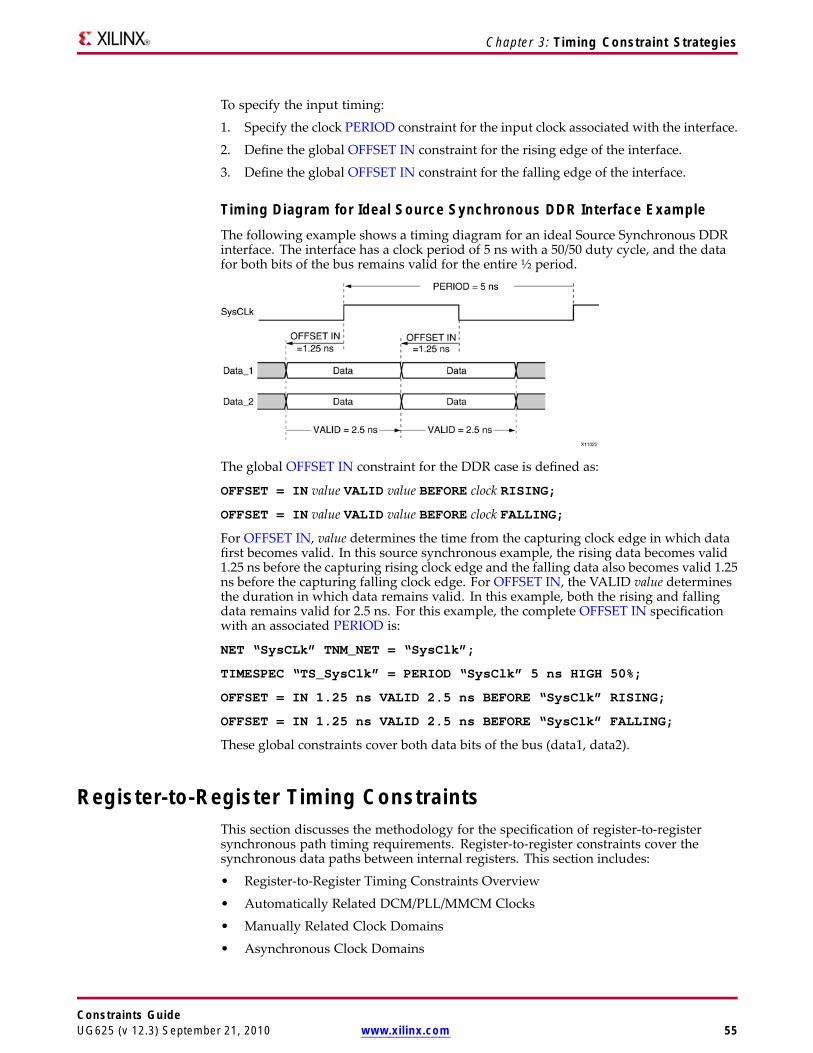
Chapter 3: Timing Constraint Strategies
To specify the input timing:
1. Specify the clock PERIOD constraint for the input clock associated with the interface.
2. Define the global OFFSET IN constraint for the rising edge of the interface.
3. Define the global OFFSET IN constraint for the falling edge of the interface.
Timing Diagram for Ideal Source Synchronous DDR Interface ExampleThe following example shows a timing diagram for an ideal Source Synchronous DDRinterface. The interface has a clock period of 5 ns with a 50/50 duty cycle, and the datafor both bits of the bus remains valid for the entire ½ period.
The global OFFSET IN constraint for the DDR case is defined as:
OFFSET = IN value VALID value BEFORE clock RISING;
OFFSET = IN value VALID value BEFORE clock FALLING;
For OFFSET IN, value determines the time from the capturing clock edge in which datafirst becomes valid. In this source synchronous example, the rising data becomes valid1.25 ns before the capturing rising clock edge and the falling data also becomes valid 1.25ns before the capturing falling clock edge. For OFFSET IN, the VALID value determinesthe duration in which data remains valid. In this example, both the rising and fallingdata remains valid for 2.5 ns. For this example, the complete OFFSET IN specificationwith an associated PERIOD is:
NET “SysCLk” TNM_NET = “SysClk”;
TIMESPEC “TS_SysClk” = PERIOD “SysClk” 5 ns HIGH 50%;
OFFSET = IN 1.25 ns VALID 2.5 ns BEFORE “SysClk” RISING;
OFFSET = IN 1.25 ns VALID 2.5 ns BEFORE “SysClk” FALLING;
These global constraints cover both data bits of the bus (data1, data2).
Register-to-Register Timing ConstraintsThis section discusses the methodology for the specification of register-to-registersynchronous path timing requirements. Register-to-register constraints cover thesynchronous data paths between internal registers. This section includes:
• Register-to-Register Timing Constraints Overview
• Automatically Related DCM/PLL/MMCM Clocks
• Manually Related Clock Domains
• Asynchronous Clock Domains
Constraints GuideUG625 (v 12.3) September 21, 2010 www.xilinx.com 55
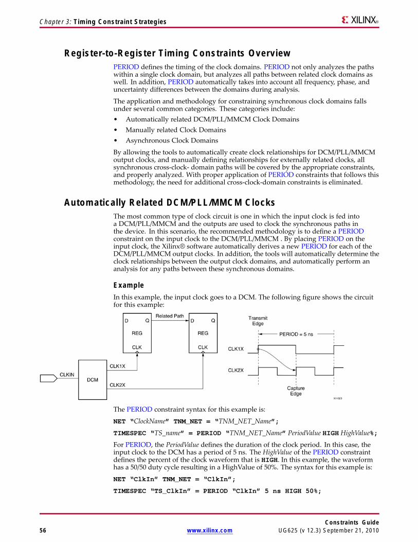
Chapter 3: Timing Constraint Strategies
Register-to-Register Timing Constraints OverviewPERIOD defines the timing of the clock domains. PERIOD not only analyzes the pathswithin a single clock domain, but analyzes all paths between related clock domains aswell. In addition, PERIOD automatically takes into account all frequency, phase, anduncertainty differences between the domains during analysis.
The application and methodology for constraining synchronous clock domains fallsunder several common categories. These categories include:• Automatically related DCM/PLL/MMCM Clock Domains• Manually related Clock Domains• Asynchronous Clock Domains
By allowing the tools to automatically create clock relationships for DCM/PLL/MMCMoutput clocks, and manually defining relationships for externally related clocks, allsynchronous cross-clock- domain paths will be covered by the appropriate constraints,and properly analyzed. With proper application of PERIOD constraints that follows thismethodology, the need for additional cross-clock-domain constraints is eliminated.
Automatically Related DCM/PLL/MMCM ClocksThe most common type of clock circuit is one in which the input clock is fed intoa DCM/PLL/MMCM and the outputs are used to clock the synchronous paths inthe device. In this scenario, the recommended methodology is to define a PERIODconstraint on the input clock to the DCM/PLL/MMCM . By placing PERIOD on theinput clock, the Xilinx® software automatically derives a new PERIOD for each of theDCM/PLL/MMCM output clocks. In addition, the tools will automatically determine theclock relationships between the output clock domains, and automatically perform ananalysis for any paths between these synchronous domains.
ExampleIn this example, the input clock goes to a DCM. The following figure shows the circuitfor this example:
The PERIOD constraint syntax for this example is:
NET “ClockName” TNM_NET = “TNM_NET_Name”;
TIMESPEC “TS_name” = PERIOD “TNM_NET_Name” PeriodValue HIGH HighValue%;
For PERIOD, the PeriodValue defines the duration of the clock period. In this case, theinput clock to the DCM has a period of 5 ns. The HighValue of the PERIOD constraintdefines the percent of the clock waveform that is HIGH. In this example, the waveformhas a 50/50 duty cycle resulting in a HighValue of 50%. The syntax for this example is:
NET “ClkIn” TNM_NET = “ClkIn”;
TIMESPEC “TS_ClkIn” = PERIOD “ClkIn” 5 ns HIGH 50%;
Constraints Guide56 www.xilinx.com UG625 (v 12.3) September 21, 2010

Chapter 3: Timing Constraint Strategies
Based on the input clock PERIOD constraint given above, the DCM automaticallycreates two output clock constraints for the DCM outputs, and automatically performsanalysis between the two domains.
Manually Related Clock DomainsIn some cases, the relationship between synchronous clock domains cannot beautomatically determined by the tools. One example occurs when related clocks enterthe FPGA device on separate pins. In this scenario, the recommended constraintmethodology is to create separate PERIOD constraints for both input clocks and definea manual relationship between the clocks. Once the manual relationship is defined,all paths between the two synchronous domains are automatically analyzed with allfrequency, phase, and uncertainty information automatically taken into account.
The Xilinx constraints system allows for complex manual relationships to be definedbetween clock domains using PERIOD. This manual relationship can include clockfrequency and phase transformations. The methodology for this process is:1. Define PERIOD for the primary clock2. Define the PERIOD constraint for the related clock using the first PERIOD constraint
as a reference
For more information on using PERIOD to define clock relationships, see Period.
ExampleIn this example two related clocks enter the FPGA device through separate externalpins. The first clock, CLK1X, is the primary clock, and the second clock, CLK2X180 is therelated clock. The circuit for this example is shown in the following figure:
The PERIOD syntax for this example is:
NET “PrimaryClock” TNM_NET = “TNM_Primary”;
NET “RelatedClock” TNM_NET = “TNM_Related”;
TIMESPEC “TS_primary” = PERIOD “TNM_Primary” PeriodValue HIGH HighValue%;
TIMESPEC “TS_related” = PERIOD “TNM_Related” TS_Primary_relation PHASEvalue;
In the related PERIOD definition, the PERIOD value is defined as a time unit (period)relationship to the primary clock. The relationship is expressed in terms of the primaryclock TIMESPEC. In this example CLK2X180 operates at twice the frequency of CLK1Xwhich results in a PERIOD relationship of ½. In the related PERIOD definition, thePHASE value defines the difference in time between the rising clock edge of the sourceclock and the related clock. In this example, the CLK2X180 clock is 180 degrees shifted,so the rising edge begins 1.25 ns after the rising edge of the primary clock. The syntaxfor this example is:
NET “Clk1X" TNM_NET = “Clk1X";
Constraints GuideUG625 (v 12.3) September 21, 2010 www.xilinx.com 57

Chapter 3: Timing Constraint Strategies
NET “Clk2X180" TNM_NET = “Clk2X180";
TIMESPEC "TS_Clk1X" = PERIOD "Clk1X" 5 ns;
TIMESPEC "TS_Clk2X180" = PERIOD "Clk2X180“ TS_Clk1X/2 PHASE +1.25 ns ;
Asynchronous Clock DomainsAsynchronous clock domains are defined as those in which the transmit and captureclocks bear no frequency or phase relationship. Because the clocks are not related, it isnot possible to determine the final relationship for setup and hold time analysis. For thisreason, it is recommended that proper asynchronous design techniques be employedto ensure the successful capture of data. However, while not required, in some casesdesigners wish to constrain the maximum data path delay in isolation without regard toclock path frequency or phase relationship.
The Xilinx constraints system allows for the constraining of the maximum data pathdelay without regard to source and destination clock frequency and phase relationship.
This requirement is specified using FROM-TO with the DATAPATHONLY keyword.
The methodology for this process is:1. Define a time group for the source registers2. Define a time group for the destination registers3. Define the maximum delay of the net using FROM-TO between the two time groups
with DATAPATHONLY keyword.
For more information on using FROM-TO with the DATAPATHONLY keyword, seeFROM-TO.
ExampleIn this example two unrelated clocks enter the FPGA device through separate externalpins. The first clock, CLKA, is the source clock, and the second clock, CLKB is thedestination clock. The circuit for this example is shown in the following figure:
NET “CLKA” TNM_NET = FFS “GRP_A”;
NET “CLKB” TNM_NET = FFS “GRP_B”;
TIMESPEC TS_Example = FROM “GRP_A” TO “GRP_B” 5 ns DATAPATHONLY;
Output Timing ConstraintsThis section discusses how to specify output timing constraints. Output timingconstraints cover the data path from a register inside the FPGA device to the externalpin of the FPGA device.
Constraints Guide58 www.xilinx.com UG625 (v 12.3) September 21, 2010

Chapter 3: Timing Constraint Strategies
Output Timing Constraints OverviewUse OFFSET OUT to specify output timing. The best way to specify the outputtiming requirements depends on the type (source/system synchronous) and data rate(SDR/DDR) of the interface.
OFFSET OUT defines the maximum time allowed for data to be transmitted from theFPGA device. The output delay path begins at the input clock pin of the FPGA deviceand continues through the output register to the data pins of the FPGA. This path isshown in the following diagram.
When analyzing OFFSET OUT, the timing analysis software automatically take allinternal factors affecting the delay of the clock and software into account. These factorsinclude:
• Frequency and phase transformations of the clock
• Clock uncertainties
• Data path delay adjustments
System Synchronous OutputThe system synchronous output interface is an interface in which a common system clockis used to both transfer and capture the data. The following figure shows a simplifiedSystem Synchronous output interface with associated single data rate (SDR) timing.
Constraints GuideUG625 (v 12.3) September 21, 2010 www.xilinx.com 59
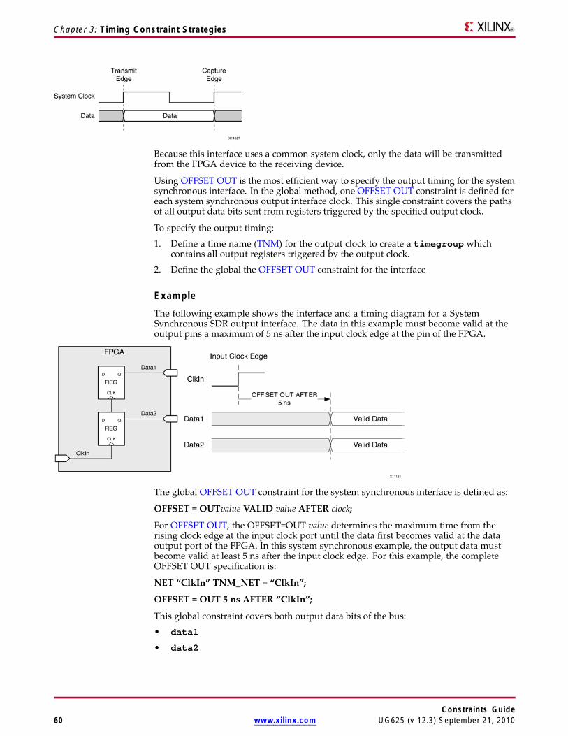
Chapter 3: Timing Constraint Strategies
Because this interface uses a common system clock, only the data will be transmittedfrom the FPGA device to the receiving device.
Using OFFSET OUT is the most efficient way to specify the output timing for the systemsynchronous interface. In the global method, one OFFSET OUT constraint is defined foreach system synchronous output interface clock. This single constraint covers the pathsof all output data bits sent from registers triggered by the specified output clock.
To specify the output timing:
1. Define a time name (TNM) for the output clock to create a timegroup whichcontains all output registers triggered by the output clock.
2. Define the global the OFFSET OUT constraint for the interface
ExampleThe following example shows the interface and a timing diagram for a SystemSynchronous SDR output interface. The data in this example must become valid at theoutput pins a maximum of 5 ns after the input clock edge at the pin of the FPGA.
The global OFFSET OUT constraint for the system synchronous interface is defined as:
OFFSET = OUTvalue VALID value AFTER clock;
For OFFSET OUT, the OFFSET=OUT value determines the maximum time from therising clock edge at the input clock port until the data first becomes valid at the dataoutput port of the FPGA. In this system synchronous example, the output data mustbecome valid at least 5 ns after the input clock edge. For this example, the completeOFFSET OUT specification is:
NET “ClkIn” TNM_NET = “ClkIn”;
OFFSET = OUT 5 ns AFTER “ClkIn”;
This global constraint covers both output data bits of the bus:
• data1
• data2
Constraints Guide60 www.xilinx.com UG625 (v 12.3) September 21, 2010

Chapter 3: Timing Constraint Strategies
Source Synchronous OutputsThe source synchronous output interface is an interface in which a clock is regeneratedand transmitted along with the data from the FPGA device. The following figure showsa simplified Source Synchronous output interface with associated DDR timing.
Because the regenerated clock is transmitted along with the data, the interface isprimarily limited in performance by system noise and the skew between the regeneratedclock and the data bits. In this interface, the time from the input clock edge to the outputdata becoming valid is not as important as the skew between the output data bits andin most cases can be left unconstrained.
Using OFFSET OUT is the most efficient way to specify the output timing for a sourcesynchronous interface. In the DDR interface, one OFFSET OUT constraint is defined foreach edge of the output interface clock. These constraints cover the paths of all outputdata bits that are transmitted by registers triggered with the specified output clock edge.
To specify the output timing:1. Define a time name (TNM) for the output clock to create a timegroup which
contains all output registers triggered by the output clock2. Define the global OFFSET OUT constraint for the rising edge of the interface3. Define the global OFFSET OUT constraint for the falling edge of the interface
ExampleThe following example shows a timing diagram for an ideal Source Synchronous DDRinterface. In this interface example the absolute clock to output time is not important,and only the skew between the regenerated clock and the output data bits is desired.
The global OFFSET OUT constraints for the DDR case are:
OFFSET = OUT AFTERclock REFERENCE_PIN "REF_CLK" RISING;
OFFSET = OUT AFTERclock REFERENCE_PIN "REF_CLK" FALLING;
Constraints GuideUG625 (v 12.3) September 21, 2010 www.xilinx.com 61

Chapter 3: Timing Constraint Strategies
For OFFSET OUT, the OFFSET=OUT value determines the maximum time from therising clock edge at the input clock port until the data first becomes valid at the dataoutput port of the FPGA device. When the value is omitted from OFFSET OUT, theconstraint becomes a report only specification which reports the skew of the output bus.The REFERENCE_PIN keyword in the constraint defines the regenerated output clock asthe reference point for which the skew of the output data pins is reported against.
For this example, the complete OFFSET OUT specification for both the rising and fallingclock edges is:
NET "ClkIn" TNM_NET = "ClkIn";
OFFSET = OUT AFTER "ClkIn" REFERENCE_PIN "ClkOut" RISING;
OFFSET = OUT AFTER "ClkIn" REFERENCE_PIN "ClkOut" FALLING;
Exception Timing ConstraintsThis section discusses Exception Timing Constraints and includes:
• Exception Timing Constraints Overview
• False Paths
• Multi-Cycle Paths
Exception Timing Constraints OverviewBy using the global definitions of the input, register-to-register, and output timingconstraints, the majority of the paths are properly constrained. However, in certain casesa small number of paths contain exceptions to the global constraint rules. The mostcommon type of exceptions specified are:
• False Paths
• Multi-Cycle Paths
False PathsIn some cases, you may want to remove a set of paths from analysis if these paths donot affect timing performance.
One common way to specify the set of paths to remove from timing analysis is to use theFROM-TO constraint with the timing ignore (TIG) keyword. This allows you to specifya set of registers in a source time group and a set of registers in a destination time group,and to automatically remove all paths between those time groups from analysis.
To specify the timing ignore (TIG) constraint for this method:
1. Define a set of registers for the source time group
2. Define a set of registers for the destination time group
3. Define a FROM-TO constraint with a TIG keyword to remove the paths betweenthe groups
ExampleThis example shows a hypothetical case in which a path between two registers doesnot affect the timing of the design, and is desired to be removed from analysis. Thefollowing figure shows a block diagram of the example circuit.
Constraints Guide62 www.xilinx.com UG625 (v 12.3) September 21, 2010

Chapter 3: Timing Constraint Strategies
The generic syntax for defining a timing ignore (TIG) between time groups is:
TIMESPEC "TSid" = FROM "SRC_GRP" TO "DST_GRP" TIG;
In the FROM-TO TIG example, the SRC_GRP defines the set of source registers inwhich path tracing will begin from while the DST_GRP defines the set of destinationregisters the path tracing will end at. All paths that begin in the SRC_GRP and end inthe DST_GRP will be ignored.
The specific syntax for this example is:
NET “CLK1” TNM_NET = FFS “GRP_1”;
NET “CLK2” TNM_NET = FFS “GRP_2”;
TIMESPEC TS_Example = FROM “GRP_1” TO “GRP_2” TIG;
Multi-Cycle PathsA multi-cycle path is a path in which data is transferred from source to destinationregister at a rate that is less than the clock frequency defined in the PERIOD specification.This scenario most often occurs when the registers are gated with a common clockenable signal. By defining a multi-cycle path, the timing constraints for these registerswill be relaxed over the default PERIOD constraint, and the implementation tools willbe able to prioritize the implementation of these paths appropriately.
To specify the FROM-TO multi-cycle constraint:1. Define a PERIOD constraint for the common clock domain2. Define a set of registers based on a common clock enable signal3. Define a FROM-TO multi-cycle constraint describing the new timing requirement
ExampleThis example shows a hypothetical case in which a path between two registers is clockedby a common clock enable signal. The clock enable is toggled at a rate that is one half ofthe reference clock. A block diagram of the example circuit is shown in the figure below.
The generic syntax for defining a multi-cycle path between time groups is:
TIMESPEC “TSid” = FROM “MC_GRP” TO “MC_GRP” value;
Constraints GuideUG625 (v 12.3) September 21, 2010 www.xilinx.com 63

Chapter 3: Timing Constraint Strategies
In the FROM-TO multi-cycle example, the MC_GRP defines the set of registers whichare driven by a common clock enable signal. All paths that begin in the MC_GRP andend in the MC_GRP will have the multi-cycle timing requirement applied to them whilepaths into and out of the MC_GRP will be analyzed with the appropriate PERIODspecification.
The specific syntax for this example is:
NET “CLK1” TNM_NET = “CLK1”;
TIMESPEC “TS_CLK1” = PERIOD “CLK1” 5 ns HIGH 50%;
ET “Enable” TNM_NET = FFS “MC_GRP”;
TIMESPEC TS_Example = FROM “MC_GRP” TO “MC_GRP” TS_CLK1*2;
Constraints Guide64 www.xilinx.com UG625 (v 12.3) September 21, 2010

Chapter 4
Xilinx ConstraintsThis chapter describes the individual constraints that can be used with Xilinx® FPGAand CPLD devices. It includes the following for each constraint:• Architecture support• Applicable elements• Description• Propagation rules• Syntax examples• Additional information, if necessary
This chapter contains the following sections:• Constraint Information• Alphabetized List of Xilinx Constraints
Constraint InformationThis chapter gives the following information for each constraint:• Architecture Support
Whether the constraint may be used with that device.• Applicable Elements
The elements to which the constraint may be applied.• Description
A brief description of the constraint, including its usage and behavior.• Propagation Rules
How the constraint is propagated.• Syntax Examples
Syntax examples for using the constraint with particular tools or methods. Notevery tool or method is listed for every constraint. If a tool or method is not listed,the constraint may not be used with it.
• Additional InformationAdditional information is provided for certain constraints.
Alphabetized List of Xilinx ConstraintsThis chapter contains information on the following Xilinx® constraints:• Area Group (AREA_GROUP)• Asynchronous Register (ASYNC_REG)• BEL (BEL)
Constraints GuideUG625 (v 12.3) September 21, 2010 www.xilinx.com 65

Chapter 4: Xilinx Constraints
• Block Name (BLKNM)• BUFG (BUFG)• Clock Dedicated Route (CLOCK_DEDICATED_ROUTE)• Collapse (COLLAPSE)• Component Group (COMPGRP)• Configuration Mode (CONFIG_MODE)• CoolCLOCK (COOL_CLK)• Data Gate (DATA_GATE)• DCI Cascade (DCI_CASCADE)• DCI Value (DCI_VALUE)• Default (DEFAULT)• DIFF_TERM (Diff_Term)• Directed Routing (DIRECTED_ROUTING)• Disable (DISABLE)• Drive (DRIVE)• Drop Specifications (DROP_SPEC)• Enable (ENABLE)• Enable Suspend (ENABLE_SUSPEND)• Fast (FAST)• Feedback (FEEDBACK)• File (FILE)• Float (FLOAT)• From Thru To (FROM-THRU-TO)• From To (FROM-TO)• FSM_STYLE (FSM Style)• Hierarchical Block Name (HBLKNM)• HIODELAY_GROUP (HIODELAY Group)• Hierarchical Lookup Table Name (HLUTNM)• HU_SET (HU Set)• Input Buffer Delay Value (IBUF_DELAY_VALUE)• IFD_DELAY_VALUE (IFD Delay Value)• IN_TERM (In Term)• Input Registers (INREG)• Internal Vref Bank (INTERNAL_VREF_BANK)• IOB (IOB)• Input Output Block Delay (IOBDELAY)• Input Output Delay Group (IODELAY_GROUP)• Input Output Standard (IOSTANDARD)• Keep (KEEP)• Keeper (KEEPER)• Keep Hierarchy (KEEP_HIERARCHY)• Location (LOC)• Locate (LOCATE)
Constraints Guide66 www.xilinx.com UG625 (v 12.3) September 21, 2010

Chapter 4: Xilinx Constraints
• Lock Pins (LOCK_PINS)• Lookup Table Name (LUTNM)• Map (MAP)• Maximum Fanout (MAX_FANOUT)• Maximum Delay (MAXDELAY)• Maximum Product Terms (MAXPT)• Maximum Skew (MAXSKEW)• MCB Performance (MCB_PERFORMANCE)• Master Input Output Delay Group (MIODELAY_GROUP)• No Delay (NODELAY)• No Reduce (NOREDUCE)• Offset In (OFFSET IN)• Offset Out (OFFSET OUT)• Open Drain (OPEN_DRAIN)• OUT_TERM (Out Term)• Period (PERIOD)• Pin (PIN)• Post CRC (POST_CRC)• Post CRC Action (POST_CRC_ACTION)• Post CRC Frequency (POST_CRC_FREQ)• Post CRC INIT Flag (POST_CRC_INIT_FLAG)• Post CRC Signal (POST_CRC_SIGNAL)• Post CRC Source (POST_CRC_SOURCE)• Priority (PRIORITY)• Prohibit (PROHIBIT)• Pulldown (PULLDOWN)• Pullup (PULLUP)• Power Mode (PWR_MODE)• Registers (REG)• Relative Location (RLOC)• Relative Location Origin (RLOC_ORIGIN)• Relative Location Range (RLOC_RANGE)• Save Net Flag (SAVE NET FLAG)• Schmitt Trigger (SCHMITT_TRIGGER)• SIM Collision Check (SIM_COLLISION_CHECK)• Slew (SLEW)• Slow (SLOW)• Stepping (STEPPING)• Suspend (SUSPEND)• System Jitter (SYSTEM_JITTER)• Temperature (TEMPERATURE)• Timing Ignore (TIG)• Timing Group (TIMEGRP)
Constraints GuideUG625 (v 12.3) September 21, 2010 www.xilinx.com 67
Chapter 4: Xilinx Constraints
• Timing Specifications (TIMESPEC)• Timing Name (TNM)• Timing Name Net (TNM_NET)• Timing Point Synchronization (TPSYNC)• Timing Thru Points (TPTHRU)• Timing Specification Identifier (TSidentifier)• U_SET (U_SET)• Use Internal VREF (USE_INTERNAL_VREF)• USE_LUTNM (Use LUTNM)• Use Low Skew Lines (USELOWSKEWLINES)• Use Relative Location (USE_RLOC)• VCCAUX (VCCAUX)• Voltage (VOLTAGE)• VREF (VREF)• Wire And (WIREAND)• XBLKNM (XBLKNM)
AREA_GROUP (Area Group)The AREA_GROUP (Area Group) constraint:• Is a design implementation constraint.• Enables partitioning of the design into physical regions for mapping, packing,
placement, and routing.• Is attached to logical blocks in the design.
The string value of the constraint identifies a named group of logical blocks thatare to be packed together by mapper and placed in the ranges if specified by PAR.If AREA_GROUP is attached to a hierarchical block, all sub-blocks in the block areassigned to the group.
Once defined, an AREA_GROUP can have a variety of additional constraints associatedwith it to control its implementation. For more information, see Constraint Syntax below.
Architecture SupportApplies to FPGA devices. Does not apply to CPLD devices.
Applicable Elements• Logic blocks• Timing groups
For more information, see Defining From Timing Groups below.
Propagation Rules• When attached to a design element, AREA_GROUP is propagated to all applicable
elements in the hierarchy below the component.• It is illegal to attach AREA_GROUP to a net, signal, or pin.
Constraints Guide68 www.xilinx.com UG625 (v 12.3) September 21, 2010

Chapter 4: Xilinx Constraints
Constraint SyntaxThe UCF syntax for defining an area group is:
INST “X ” AREA_GROUP=groupname ;
The UCF syntax for attaching constraints to an area group is:
AREA_GROUP “groupname” RANGE=range;
or
AREA_GROUP “groupname” COMPRESSION=percent;
or
AREA_GROUP “groupname” GROUP={OPEN|CLOSED};
or
AREA_GROUP “groupname ”PLACE={OPEN|CLOSED};
wheregroupname is the name assigned to an implementation partition to uniquely define thegroup.
Each of these additional AREA_GROUP constraints is described below.
RANGE
RANGE defines the range of device resources that are available to place logiccontained in the AREA_GROUP, in the same manner ranges are defined for theLOC constraint.
For all FPGA devices, the RANGE syntax is as follows:
RANGE=SLICE_X# Y#:SLICE_X#Y#
RANGE=RAMB16_X#Y#:RAMB16_X#Y#
RANGE=MULT18X18_X #Y#:MULT18X18_X#Y#
All FPGA devices SLICES are supported. If an AREA_GROUP contains both BlockRAM and SLICE elements, two separate AREA_GROUP RANGE components canbe specified: one for BRAM elements and one for SLICE elements.
All locations in the FPGA device are specified in terms of X and Y coordinates. Youcan use the wildcard character for either the X coordinate or the Y coordinate.
The RANGE value can also be specified as a CLOCK REGION element or a set ofCLOCK REGION elements. This syntax is supported for all INST types that canbe used in AREA_GROUP constraints.
For all FPGA devices, AREA_GROUP is supported for various clock regions:
For a single region:
AREA_GROUP “groupname” RANGE=CLOCKREGION_X#Y#;
For a range of clock regions that form a rectangle:
AREA_GROUP "group_name"RANGE=CLOCKREGION_X#Y#:CLOCKREGION_X#Y#;
For a list of clock regions:
AREA_GROUP “groupname”RANGE=CLOCKREGION_X#Y#,CLOCKREGION_X#Y#,...,;
The valid X# and Y# values vary by device.Types of Logic Legal in the RANGE Constraint
Constraints GuideUG625 (v 12.3) September 21, 2010 www.xilinx.com 69

Chapter 4: Xilinx Constraints
Range Name virtex4 virtex5 virtex6 spartan6BSCAN_XnYn X X X X
BUFDS_XnYn X X
BUFGCTRL_XnYn X X X
BUFGMUX_XnYn X
BUFHCE_XnYn X
BUFH_XnYn X
BUFIO2FB_XnYn X
BUFIO2_XnYn X
BUFIODQS_XnYn X
BUFIO_XnYn X X
BUFO_XnYn X
BUFPLL_MCB_XnYn X
BUFPLL_XnYn X
BUFR_XnYn X X X
CAPTURE_XnYn X
CFG_IO_ACCESS_XnYn X
CRC32_XnYn X
CRC64_XnYn X
DCIRESET_XnYn X
DCI_XnYn X X X
DCM_ADV_XnYn X X
DCM_XnYn X
DNA_PORT_XnYn X
DPM_XnYn X
DSP48_XnYn X X X X
EFUSE_USR_XnYn X
EMAC_XnYn X
FIFO16_XnYn X
GLOBALSIG_XnYn X X X
GT11CLK_XnYn X
GT11_XnYn X
GTPA1_DUAL_XnYn X
GTP_DUAL_XnYn X
GTXE1_XnYn X
GTX_DUAL_XnYn X
IBUFDS_GTXE1_XnYn X
ICAP_XnYn X X X X
IDELAYCTRL_XnYn X X X
Constraints Guide70 www.xilinx.com UG625 (v 12.3) September 21, 2010

Chapter 4: Xilinx Constraints
Range Name virtex4 virtex5 virtex6 spartan6ILOGIC_XnYn X X X X
IOB_XnYn X X X
IODELAY_XnYn X X X
IPAD_XnYn X X X X
MCB_XnYn X
MMCM_ADV_XnYn X
MONITOR_XnYn X
OCT_CAL_XnYn X
OLOGIC_XnYn X X X X
OPAD_XnYn X X X X
PCIE_XnYn X X X
PCILOGIC_XnYn X
PLL_ADV_XnYn X X
PMCD_XnYn X
PMVBRAM_XnYn X X
PMVIOB_XnYn X
PMV_XnYn X
PPC405_ADV_XnYn X
PPC440_XnYn X
PPR_FRAME_XnYn X
RAMB16_XnYn X X
RAMB18_XnYn X
RAMB36_XnYn X X
RAMB8_XnYn X
SLICE_XnYn X X X X
STARTUP_XnYn X
SYSMON_XnYn X X
TEMAC_XnYn X X
TIEOFF_XnYn X X X X
USR_ACCESS_XnYn X
Constraints GuideUG625 (v 12.3) September 21, 2010 www.xilinx.com 71

Chapter 4: Xilinx Constraints
Sites That Do Not Conform to the Normal X, Y Format
The following sites do not conform to the normal X, Y format and can be usedin an area group range. The syntax is:
AREA_GROUP "group" RANGE=site1; AREA_GROUP "group" RANGE=site2;
Site Name virtex4 virtex5 virtex6 spartan6CAPTURE X X
DCIRESET X X
DNA_PORT X
EFUSE_USR X
FRAME_ECC X X X
JTAGPPC X X
KEY_CLEAR X
PAD X
PMV X X X
POST_CRC_INTERNAL X
SLAVE_SPI X
SPI_ACCESS X
STARTUP X X X
SUSPEND_SYNC X
USR_ACCESS_SITE X X
Constraints Guide72 www.xilinx.com UG625 (v 12.3) September 21, 2010

Chapter 4: Xilinx Constraints
COMPRESSION
COMPRESSION defines the compression factor for the AREA_GROUP constraints.The percent values can be from 0 to 100. If the AREA_GROUP does not have aRANGE, only 0 (no compression) and 1 (maximum compression) are meaningful.The mapper computes the number of CLBs in the AREA_GROUP from the RANGEand attempts to compress the logic into the percentage specified. Compression doesnot apply to BRAMs, or DSP block/multipliers.
The compression factor is similar to the -c option in MAP, except that it operateson the AREA_GROUP instead of the whole design. AREA_GROUP compressioninteracts with the -c map option as follows:• Area groups with a compression factor are not affected by the -c option. (Logic
that is not part of an area group is not merged with grouped logic if theAREA_GROUP has its own compression factor.)
• Area groups without a compression factor are affected by the -c option. Themapper may attempt to combine ungrouped logic with logic that is part of anarea group without a compression factor.
• At no time is the logic from two separate area groups combined.• The -c map option does not force compression among slices in the same area
group.
The Map Report (MRP) includes a section that summarizes AREA_GROUPprocessing.
If a symbol that is part of an AREA_GROUP contains a LOC constraint, the mapperremoves the symbol from the area group and processes the LOCconstraint.
Logic that does not belong to any AREA_GROUP can be pulled into the region oflogic belonging to an area group, as well as being packed or merged with suchlogic to form SLICES.
COMPRESSION on AREA_GROUP constraints does not apply when TimingDriven Packing and Placement is in MAP(-timing).
COMPRESSION on AREA_GROUP constraints is not supported for Virtex®-5devices.
GROUP
GROUP controls the packing of logic into physical components (that is, slices) asfollows.CLOSEDDo not allow logic outside the AREA_GROUP to be combined with logic insidethe AREA_GROUP.OPENAllow logic outside the AREA_GROUP to be combined with logic inside theAREA_GROUP.The default value is GROUP=OPEN.
PLACE
PLACE controls the allocation of resources in the area group’s RANGE, as follows.CLOSEDDo not allow comps that are not members of the AREA_GROUP to be placed withinthe RANGE defined for the AREA_GROUP.OPENAllow comps that are not members of the AREA_GROUP to be placed within theRANGE defined for the AREA_GROUP.The default value is PLACE=OPEN.
Constraints GuideUG625 (v 12.3) September 21, 2010 www.xilinx.com 73

Chapter 4: Xilinx Constraints
Syntax ExamplesThe following examples show how to use this constraint with particular tools ormethods. If a tool or method is not listed, you cannot use this constraint with it.
Schematic Syntax• Attach AREA_GROUP=groupname to a valid instance.• Attach RANGE =range to a CONFIG symbol.• Attach COMPRESSION=percent to a CONFIG symbol.• Attach GROUP={OPEN|CLOSED} to a CONFIG symbol.• Attach PLACE={OPEN|CLOSED} to a CONFIG symbol.• Attach to a CONFIG symbol. For a value of TRUE, PLACE, and GROUP must
both be CLOSED.• Attribute Names
– AREA_GROUP– RANGE range– COMPRESSION percent– GROUP={OPEN|CLOSED}– PLACE={OPEN|CLOSED}
• Attribute Values:– groupname– range– percent– GROUP={OPEN|CLOSED}– PLACE={OPEN|CLOSED}
UCF and NCF SyntaxThe following example:• Assigns all the logical blocks in state_machine_X to the area group group1• Places logic in the physical area between:
– SLICE row 1, column 1, and– SLICE row 10, column 10
INST “state_machine_X” AREA_GROUP=group1;AREA_GROUP “group1”RANGE=SLICE_X1Y1:SLICE_X10Y10;
PlanAhead™ SyntaxFor more information about using the PlanAhead™ software to create constraints, seeFloorplanning the Design in the PlanAhead User Guide. See PlanAhead in this Guide forinformation about:• Defining placement constraints• Assigning placement constraints• Defining I/O pin configurations• Floorplanning and placement constraints
Constraints Editor SyntaxFor information on setting constraints in Constraints Editor, including syntax, see theConstraints Editor Help.
Constraints Guide74 www.xilinx.com UG625 (v 12.3) September 21, 2010

Chapter 4: Xilinx Constraints
Defining From Timing GroupsTo create an area group based on a timing group, use the following UCF and NCF syntax:
TIMEGRP timing_group_name AREA_GROUP = area_group_name ;
where
• timing_group_name is the name of a previously defined timing group
• area_group_name is the name of a new area group to be defined from the TIMEGRPcontents
This is equivalent to manually assigning each member of the timing group toarea_group_name. The area group name defined by this statement can be used in RANGEconstraints, just like any other area group name.
In the AREA_GROUP definition, the timing_group_name is generally TNM_NET group,which allows area groups to be formed based on the loads of clock or other controlnets. Defining AREA_GROUP constraints from TIMEGRP constraints is useful forimproving placement of designs with many different clock domains in devices that havemore clocks than clock regions.
You can also specify a TNM group name, or the name of a user group defined by aTIMEGRP statement. Edge qualifiers used in the TIMEGRP definition are ignored whendetermining area group membership. In all cases, the AREA_GROUP members aredetermined after the TIMEGRP has been propagated to its target elements.
Since TIMEGRP constraints can contain only synchronous elements and pads, areagroups defined from timing groups also contain only these element types. If anAREA_GROUP is defined by a TIMEGRP that contains only flip-flops or latches,assigning a RANGE to that group makes sense only if ungrouped logic is also allowedwithin the area. Therefore, COMPRESSION should not be defined for such groups.
If a TNM_NET is used by a PERIOD specification, and is traced into any DCM, PLL, orMMCM, new TNM_NET groups and PERIOD specifications are created at the DCM, PLL, orMMCM outputs. If the original TNM_NET is used to define an area group, and if morethan one clock tap is used on the DCM, PLL, or MMCM, the area group is split into separategroups at each clock tap.
For example, assume you have the following UCF constraints:
NET "clk" TNM_NET="clock";
TIMESPEC "TS_clk" = PERIOD "clock" 10 MHz;
TIMEGRP "clock" AREA_GROUP="clock_area";
If the net clk is traced into a DCM, PLL, or MMCM, a new group and PERIOD specificationis created at each clock tap. Likewise, a new area group is created at each clocktap, with a suffix indicating the clock tap name. If the CLK0 and CLK2X taps wereused, the AREA_GROUP clock_area_CLK0 and clock_area_CLK2X are definedautomatically.
When AREA_GROUP definitions are split in this manner, NGDBuild issues aninformational message, showing the names of the new groups. These new group names,rather than the originally specified one, should be used in RANGE constraints.
Constraints GuideUG625 (v 12.3) September 21, 2010 www.xilinx.com 75

Chapter 4: Xilinx Constraints
ASYNC_REG (Asynchronous Register)The ASYNC_REG (Asynchronous Register) constraint:• Is a timing constraint.• Is used to improve the behavior of asynchronously clocked data for simulation.• Disables X propagation during timing simulation. In the event of a timing violation,
the previous value is retained on the output instead of going unknown.
Architecture SupportApplies to FPGA devices. Does not apply to CPLD devices.
Applicable Elements• Can be attached to registers and latches only• Should be used only on registers or latches with asynchronous inputs (D input or
the CE input.
Propagation RulesApplies to the register or latch to which it is attached.
Syntax ExamplesThe following examples show how to use this constraint with particular tools ormethods. If a tool or method is not listed, you cannot use this constraint with it.
VHDL SyntaxDeclare the VHDL constraint as follows:
attribute ASYNC_REG : string;
Specify the VHDL constraint as follows:
attribute ASYNC_REG of instance_name: label is "{TRUE|FALSE}";
For more information about basic VHDL syntax, see VHDL Attributes.
Verilog SyntaxPlace the Verilog constraint immediately before the module or instantiation.
Specify the Verilog constraint as follows:
(* ASYNC_REG = " {TRUE | FALSE}" *)
For more information about basic Verilog syntax, see Verilog Attributes.
UCF and NCF SyntaxINST “ instance_name” ASYNC_REG = {TRUE | FALSE};
The default is FALSE.
If no Boolean value is supplied it is considered TRUE.
Constraints Editor SyntaxFor information on setting constraints in Constraints Editor, including syntax, see theConstraints Editor Help.
Constraints Guide76 www.xilinx.com UG625 (v 12.3) September 21, 2010

Chapter 4: Xilinx Constraints
BEL (BEL)The BEL (BEL) constraint:• Is an advanced placement constraint.• Locks a logical symbol to a particular BEL site in a slice, or an IOB.• Differs from the Location (LOC) constraint in that LOC allows specification to the
component level. Examples of components include:– SLICE
– BRAM
– ILOGIC
– OLOGIC
– IOB
• Allows specification as to which particular BEL site of the component to be used. Forexample, this can be used to specify the specific LUT or FF to be used within a SLICE.
• Should always be used with an appropriate LOC or RLOC attribute.
An IOB BEL constraint does not direct the mapper to pack the register into an IOBcomponent. Some other feature (the -pr switch, for example) must cause the packing.Once the register is directed to an IOB, the BEL constraint causes the proper placementwithin the IOB.
The values for this constraint are:
F, G, FFA, FFB, FFC, FFD, FFX, FFY, XORF, XORG, A6LUT, B6LUT,C6LUT, D6LUT A5LUT, B5LUT, C5LUT, D5LUT
where• F, G, A6LUT, B6LUT, C6LUT, D6LUT, A5LUT, B5LUT, C5LUT and D5LUT
identify specific LUTs, SRL16s, distributed RAM components in the slice• FFX, FFY, FFA, FFB, FFC and FFD identify specific flip-flops, latches, and
other elements in a slice• XORF and XORG identify XORCY elements in a slice
The following values are also valid for Virtex®-6 devices:
AFF, BFF, CFF, DFF, A5FF, B5FF, C5FF, D5FF
Architecture SupportApplies to FPGA devices. Does not apply to CPLD devices.
Applicable ElementsRegisters LatchesLUT
LUTRAM
RAMB18
SRL
Propagation RulesIt is legal to place a BEL constraint only on an appropriate instance with a valid LOCor RLOC.
Constraints GuideUG625 (v 12.3) September 21, 2010 www.xilinx.com 77
Chapter 4: Xilinx Constraints
Syntax ExamplesThe following examples show how to use this constraint with particular tools ormethods. If a tool or method is not listed, you cannot use this constraint with it.
Schematic Syntax• Attach to a valid instance• Attribute Name
BEL
VHDL SyntaxDeclare the VHDL constraint as follows:
attribute bel : string;
Specify the VHDL constraint as follows:
attribute bel of {component_name| label_name}: {component|label} is "{value}";
For more information about basic VHDL syntax, see VHDL Attributes.
Verilog SyntaxPlace the Verilog constraint immediately before the module or instantiation.
Specify the Verilog constraint as follows:
(* BEL = " {value}" *)
For more information about basic Verilog syntax, see Verilog Attributes.
UCF and NCF SyntaxINST "instance_name " BEL={value};
The syntax for the RAMB BEL instance is:
INST "upper_BRAM_instance_name" LOC = RAMB36_XnYn | BEL = UPPER;
INST "lower_BRAM_instance_name" LOC = RAMB36_XnYn | BEL = LOWER;
ExampleINST "ramb18_inst0" LOC = RAMB36_X0Y2 | BEL = UPPER; INST "ramb18_inst1"LOC = RAMB36_X0Y2 | BEL = LOWER;
The following statement locks xyzzy to the FFX site on the slice.
INST "xyzzy" BEL=FFX;
PlanAhead™ SyntaxFor more information about using the PlanAhead™ software to create constraints, seeFloorplanning the Design in the PlanAhead User Guide. See PlanAhead in this Guide forinformation about:• Defining placement constraints• Assigning placement constraints• Defining I/O pin configurations• Floorplanning and placement constraints
Constraints Guide78 www.xilinx.com UG625 (v 12.3) September 21, 2010

Chapter 4: Xilinx Constraints
BLKNM (Block Name)The BLKNM (Block Name) constraint:
• Is an advanced mapping constraint
• Assigns block names to qualifying primitives and logic elements.
If the same BLKNM constraint is assigned to more than one instance, the softwareattempts to map them into the same block. Conversely, two symbols with differentBLKNM names are not mapped into the same block. Placing similar BLKNM constraintson instances that do not fit within one block causes an error.
Specifying identical BLKNM constraints on FMAP tells the software to group theassociated function generators into a single SLICE. Using BLKNM, you can partition acomplete SLICE without constraining the SLICE to a physical location on the device.BLKNM constraints, like LOC constraints, are specified from the design. Sincehierarchical paths are not prefixed to BLKNM constraints, BLKNM constraints fordifferent SLICEs must be unique throughout the entire design. For information onattaching hierarchy to block names, see Hierarchical Block Name (HBLKNM).
BLKNM allows any elements except those with a different BLKNM to be mappedinto the same physical component. Elements without a BLKNM can be packed withthose that have a BLKNM. For information on allowing only elements with the sameXBLKNM to be mapped into the same physical component, see XBLKNM.
Architecture SupportApplies to FPGA devices. Does not apply to CPLD devices.
Applicable ElementsThis constraint may be used with an FPGA device in one or more of the following designelements, or categories of design elements. Not all devices support all elements. To seewhich design elements can be used with which devices, see the Libraries Guides. Formore information, see the device data sheet.
• Flip-flop and latch primitives
• Any I/O element or pad
• FMAP
• ROM primitives
• RAMS and RAMD primitives
• Carry logic primitives
• Block RAM
You can also attach BLKNM to the net connected to the pad component in a UserConstraints File (UCF) file. NGDBuild transfers the constraint from the net to the padinstance in the NGD file so that it can be processed by the mapper. Use the followingsyntax:
NET “net_name” BLKNM=property_value;
Propagation RulesWhen attached to a design element, this constraint is propagated to all applicableelements in the hierarchy within the design element.
Constraints GuideUG625 (v 12.3) September 21, 2010 www.xilinx.com 79

Chapter 4: Xilinx Constraints
Syntax ExamplesThe following examples show how to use this constraint with particular tools ormethods. If a tool or method is not listed, you cannot use this constraint with it.
Schematic Syntax• Attach to a valid instance
• Attribute Name
BLKNM
• Attribute Value
block_name
VHDL SyntaxDeclare the VHDL constraint as follows:
attribute blknm : string;
Specify the VHDL constraint as follows:
attribute blknm of {component_name|signal_name|entity_name|label_name}:{component|signal|entity|label} is “block_name”;
For more information about basic VHDL syntax, see VHDL Attributes.
Verilog SyntaxPlace the Verilog constraint immediately before the module or instantiation.
Specify the Verilog constraint as follows:
(* BLKNM = “blk_name” *)
For more information about basic Verilog syntax, see Verilog Attributes.
UCF and NCF SyntaxINST “instance_name” BLKNM=block_name;
where
block_name is a valid block name for that type of symbol
For information on assigning hierarchical block names, see Hierarchical Block Name(HBLKNM).
The following statement assigns an instantiation of an element named block1 toa block named U1358.
INST “$1I87/block1” BLKNM=U1358;
XCF SyntaxMODEL “entity_name” blknm = block_name;
BEGIN MODEL “entity_name”
INST "instance_name" blknm = block_name;
END;
Constraints Guide80 www.xilinx.com UG625 (v 12.3) September 21, 2010

Chapter 4: Xilinx Constraints
BUFG (BUFG)The BUFG (BUFG) constraint:• Is an advanced fitter constraint.• Is a synthesis constraint.When applied to an input buffer or input pad net, BUFG maps the tagged signal to aglobal net. When applied to an internal net, the tagged signal is either routed directly toa global net or brought out to a global control pin to drive the global net, as supportedby the target device family architecture.
This constraint has the following values:
• CLK
Maps to a global clock (GCK) line• OE
Maps to a global tristate control (GTS) line• SR
Maps to a global set/reset control (GSR) line• DATA_GATE
Maps to the DATA_GATE latch enable control line
Architecture SupportApplies to CPLD devices only. Does not apply to FPGA devices.
Applicable ElementsAny input buffer (IBUF), input pad net, or internal net that drives a CLK, OE, SR, orDATA_GATE pin
Propagation RulesWhen attached to a net, BUFG has a net or signal form and so no special propagationis required. When attached to a design element, BUFG is propagated to all applicableelements in the hierarchy within the design element.
Syntax ExamplesThe following examples show how to use this constraint with particular tools ormethods. If a tool or method is not listed, you cannot use this constraint with it.
Schematic Syntax• Attach to an IBUF instance of the input pad connected to an IBUF input• Attribute Name
BUFG
VHDL SyntaxDeclare the VHDL constraint as follows:
attribute BUFG: string;
Specify the VHDL constraint as follows:
attribute BUFG of signal_name : signal is “{CLK|OE |SR|DATA_GATE} ”;
Constraints GuideUG625 (v 12.3) September 21, 2010 www.xilinx.com 81

Chapter 4: Xilinx Constraints
For more information about basic VHDL syntax, see VHDL Attributes.
Verilog SyntaxPlace the Verilog constraint immediately before the module or instantiation.
Specify the Verilog constraint as follows:
(* BUFG = "{CLK | OE | SR | DATA_GATE}" *)
For more information about basic Verilog syntax, see Verilog Attributes.
UCF and NCF SyntaxNET “net_name ” BUFG={CLK | OE | SR | DATA_GATE};
INST “instance_name” BUFG={CLK | OE | SR| DATA_GATE};
where• CLK
Designates a global clock pin (all CPLD families)• OE
Designates a global tristate control pin (all CPLD devices except CoolRunner™-IIand CoolRunner XPLA3 devices) or internal global tristate control line(CoolRunner-II devices only)
• SR
Designates a global set/reset pin (all CPLD devices except CoolRunner-II andCoolRunner XPLA3 devices)
• DataGate
Maps to the DataGate latch enable control line
The following statement maps the signal named fastclk to a global clock net.
NET “fastclk” BUFG=CLK;
XCF SyntaxBEGIN MODEL “entity_name ”
NET "signal_name" BUFG = {CLK|OE |SR|DATA_GATE} ;
END;
Clock Dedicated Route (CLOCK_DEDICATED_ROUTE)The Clock Dedicated Route (CLOCK_DEDICATED_ROUTE) constraint:• Is an advanced constraint.• Directs the tools whether or not to follow clock placement rules for a specific
architecture.If the constraint is not used or set to TRUE, clock placement rules must be followed.Otherwise, placement will error. If the constraint is set to FALSE, it directs the tools toignore the specific clock placement rule and continue with Place and Route (PAR). Ifpossible, all clock placement rule violations should be fixed in a design in order toensure the best clocking performance. This constraint is intended to be used only inlimited situations when it is absolutely necessary to violate a clock placement rule. Formore information about specific clock placement rules, see the Hardware User’s Guide.
Constraints Guide82 www.xilinx.com UG625 (v 12.3) September 21, 2010
Chapter 4: Xilinx Constraints
Architecture SupportApplies to FPGA devices. Does not apply to CPLD devices.
Applicable Elements• Nets• Input and output pins of the following primitives:
– BUFG
– BUFR
– DCM
– PLLPMCD
– GT11
– GT11 DUAL
– GT11 CLK
– GTP DUAL
Propagation RulesApplies to the NET or INSTANCE PIN.
Syntax ExamplesThe following examples show how to use this constraint with particular tools ormethods. If a tool or method is not listed, you cannot use this constraint with it.
Schematic Syntax• Attach to a valid instance• Attribute Name
CLOCK_DEDICATED_ROUTE
• Attribute Values– TRUE
– FALSE
UCF and NCF SyntaxPIN "BEL_INSTANCE_NAME.PIN " CLOCK_DEDICATED_ROUTE = {TRUE | FALSE};
whereBEL_INSTANCE_NAME.PIN is the specific input/output pin of the instance you want toconstrain. An example is the CLKIN input pin of a DCM instance.
COLLAPSE (Collapse)The COLLAPSE (Collapse) constraint:• Is an advanced fitter constraint.• Forces a combinatorial node to be collapsed into all of its fanouts.
Architecture SupportApplies to CPLD devices only. Does not apply to FPGA devices.
Constraints GuideUG625 (v 12.3) September 21, 2010 www.xilinx.com 83

Chapter 4: Xilinx Constraints
Applicable ElementsAny internal net.
Propagation RulesThis constraint is a net constraint. Any attachment to a design element is illegal.
Syntax ExamplesThe following examples show how to use this constraint with particular tools ormethods. If a tool or method is not listed, you cannot use this constraint with it.
Schematic Syntax• Attach to a logic symbol or its output net• Attribute Name
COLLAPSE
• Attribute Values– TRUE
– FALSE
VHDL SyntaxDeclare the VHDL constraint as follows:
attribute collapse: string;
Specify the VHDL constraint as follows:
attribute collapse of signal_name: signal is “{YES|NO|TRUE|FALSE}”;
For more information about basic VHDL syntax, see VHDL Attributes.
Verilog SyntaxPlace the Verilog constraint immediately before the module or instantiation.
Specify the Verilog constraint as follows:
(* COLLAPSE = “{YES|NO|TRUE|FALSE}” *)
For more information about basic Verilog syntax, see Verilog Attributes.
UCF and NCF SyntaxNET “net_name” COLLAPSE;
The following statement forces net $1N6745 to collapse into all its fanouts.
NET “$1I87/$1N6745” COLLAPSE;
COMPGRP (Component Group)The COMPGRP (Component Group) constraint:• Is an advanced grouping constraint• Identifies a group of components
Architecture SupportApplies to FPGA devices. Does not apply to CPLD devices.
Constraints Guide84 www.xilinx.com UG625 (v 12.3) September 21, 2010

Chapter 4: Xilinx Constraints
Applicable ElementsGroups of components.
Syntax ExamplesThe following examples show how to use this constraint with particular tools ormethods. If a tool or method is not listed, you cannot use this constraint with it.
PCF SyntaxCOMPGRP “group_name”=comp_item1... comp_itemn [EXCEPT comp_group];
where
comp_item is one of the following
– COMP “comp_name”
– COMPGRP “group_name”
CONFIG_MODE (Configuration Mode)The CONFIG_MODE (Configuration Mode) constraint:
• Communicates to PAR which of the dual purpose configuration pins can be usedas general purpose IOs.
• Is used by PAR to prohibit the use of Dual Purpose IOs if they are required forCONFIG_MODE: S_SELECTMAP+READBACK or M_SELECTMAP+READBACK.
In the case of CONFIG_MODE: S_SELECTMAP or M_SELECTMAP, PAR uses the DualPurpose IOs as General Purpose IOs only if necessary.
Architecture SupportApplies to Spartan®-3, Virtex®-4, Virtex-5, and Virtex-6 devices.
Applicable ElementsAttaches to the CONFIG symbol.
Propagation RulesApplies to dual-purpose I/Os.
Syntax ExamplesThe following examples show how to use this constraint with particular tools ormethods. If a tool or method is not listed, you cannot use this constraint with it.
UCF SyntaxCONFIG CONFIG_MODE=string;
Constraints GuideUG625 (v 12.3) September 21, 2010 www.xilinx.com 85

Chapter 4: Xilinx Constraints
wherestring can be one of the following:– S_SERIAL
Slave Serial Mode– M_SERIAL
Master Serial Mode (The default value)– S_SELECTMAP
Slave SelectMAP Mode– M_SELECTMAP
Master SelectMAP Mode.– B_SCAN
Boundary Scan Mode– S_SELECTMAP+READBACK
Slave SelectMAP Mode with Persist set to support Readback and Reconfiguration.– M_SELECTMAP+READBACK
Master SelectMAP Mode with Persist set to support Readback and Reconfiguration.– B_SCAN+READBACK
Boundary Scan Mode with Persist set to support Readback and Reconfiguration– S_SELECTMAP32+READBACK
Slave SelectMAP Mode with Persist set to support Readback and Reconfiguration.– S_SELECTMAP32
Slave SelectMAP32 ModeFor S_SELECTMAP32 and S_SELECTMAP32+READBACK, you can selectS_SELECTMAP16 and S_SELECTMAP16+READBACK for Virtex-5 devices to have thecorrect number of data pins needed persisting after configuration.
COOL_CLK (CoolCLOCK)COOL_CLK (CoolCLOCK) reduces clocking power within a CPLD device by combiningclock division circuitry with the DualEDGE circuitry. Because the clock net can be asignificant power drain, the clock power can be reduced by driving the net at halffrequency, then doubling the clock rate using DualEDGE triggered macrocells.
Architecture SupportApplies to CoolRunner™-II devices only.
Applicable ElementsApplies to any input pad or internal signal driving a register clock.
Propagation RulesApplying COOL_CLK to a clock net is equivalent to passing the clock through adivide-by-two clock divider (CLK_DIV2) and replacing all flip-flops controlled by thatclock with DualEDGE flip-flops. Using COOL_CLK does not alter your overall designfunctionality.
Constraints Guide86 www.xilinx.com UG625 (v 12.3) September 21, 2010

Chapter 4: Xilinx Constraints
Some restrictions apply:• You cannot use COOL_CLK on a clock that triggers any flip-flop on the low-going
edge. The CoolRunner™-II clock divider can be triggered only on the high-risingedge of the clock signal.
• If there are any DualEDGE flip-flops in your design source, the clock that controlsany of them cannot be specified as a COOL_CLK.
• If there is already a clock divider in your design source, you cannot also useCOOL_CLK. CoolRunner-II devices contain only one clock divider.
Syntax ExamplesThe following examples show how to use this constraint with particular tools ormethods. If a tool or method is not listed, you cannot use this constraint with it.
Schematic Syntax• Attach to a input pad or internal signal driving a register clock• Attribute Name
COOL_CLK
• Attribute Values– TRUE
– FALSE
VHDL SyntaxDeclare the VHDL constraint as follows:
attribute cool_clk: string;
Specify the VHDL constraint as follows:
attribute cool_clk of signal_name: signal is “{TRUE | FALSE}”;
For more information about basic VHDL syntax, see VHDL Attributes.
Verilog SyntaxPlace the Verilog constraint immediately before the module or instantiation.
Specify the Verilog constraint as follows:
(* COOL_CLK = “{TRUE | FALSE}” *)
For more information about basic Verilog syntax, see Verilog Attributes.
UCF and NCF SyntaxNET “signal_name” COOL_CLK;
DATA_GATE (Data Gate)DATA_GATE (Data Gate) provides a direct means of reducing power consumption.Each I/O pin input signal passes through a latch that can block the propagation ofincident transitions during periods when such transitions are not of interest to yourCPLD design. Input transitions that do not affect the CPLD design function stillconsume power, if not latched, as they are routed among the device’s function blocks.By asserting the DATA_GATE control I/O pin on the device, selected I/O pin inputsbecome latched, thereby eliminating the power dissipation associated with externaltransitions on those pins.
Constraints GuideUG625 (v 12.3) September 21, 2010 www.xilinx.com 87

Chapter 4: Xilinx Constraints
Architecture SupportApplies to CoolRunner™-II devices with 128 macrocells or more only.
Applicable ElementsI/O pads and pins
Propagation RulesApplying the DATA_GATE attribute to any I/O pad indicates that the pass-through latchon that device pin is to respond to the DATA_GATE control line. Any I/O pad (exceptthe DATA_GATE control I/O pin itself), including clock input pads, can be configured toget latched by applying the DATA_GATE attribute. All other I/O pads that do not have aDATA_GATE attribute remain unlatched at all times. The DATA_GATE control signalitself can be received from off-chip via the DATA_GATE I/O pin, or you can generateit in your design based on inputs that remain unlatched (pads without DATA_GATEattributes).
For more information on using DATA_GATE with Verilog and VHDL designs, seeBUFG (BUFG).
Syntax ExamplesThe following examples show how to use this constraint with particular tools ormethods. If a tool or method is not listed, you cannot use this constraint with it.
Schematic Syntax• Attach to I/O pads and pins• Attribute Name
DATA_GATE
• Attribute Values– TRUE
– FALSE
VHDL SyntaxDeclare the VHDL constraint as follows:
attribute DATA_GATE : string;
Specify the VHDL constraint as follows:
attribute DATA_GATE of signal_name: signal is “{TRUE|FALSE}”;
For more information about basic VHDL syntax, see VHDL Attributes.
Verilog SyntaxPlace the Verilog constraint immediately before the module or instantiation.
Specify the Verilog constraint as follows:
(* DATA_GATE = “{TRUE|FALSE}” *)
For more information about basic Verilog syntax, see Verilog Attributes.
UCF and NCF SyntaxNET “signal_name” DATA_GATE;
Constraints Guide88 www.xilinx.com UG625 (v 12.3) September 21, 2010

Chapter 4: Xilinx Constraints
XCF SyntaxBEGIN MODEL “entity_name”
NET “signal_name” data_gate={TRUE|FALSE};
END ;
DCI Cascade (DCI_CASCADE)In Virtex®-5 and Virtex-6 device families, IO banks that need DCI reference voltagecan be cascaded with other DCI IO banks. One set of VRN/VRP pins can be used toprovide reference voltage to several IO banks. This results in more usable pins andin reduced power usage because fewer VR pins and DCI controllers are used. DCICascade (DCI_CASCADE) identifies a DCI master bank and its corresponding slavebanks. There can be multiple instances of this constraint for a design in order to specifymultiple master-slave pairs. BitGen uses information from this constraint to programDCI controllers for different banks and have them cascade up or down. The placeralso uses this information to determine whether VR pins in slave banks can be usedfor other purposes.
Each instance of DCI_CASCADE must have one master bank and one or more slavebanks that can be entered as a space-separated list. The first value in the list is the masterbank and all subsequent values are slave banks that get DCI reference voltage from themaster bank. Cascaded banks must be in the same column (left, center or right) and musthave the same VCCO setting. For more information, see UCF and NCF Syntax below.
Architecture SupportApplies to Virtex-5 and Virtex-6 devices only.
Applicable ElementsA DCI_CASCADE attribute on the top level design block.
Propagation RulesPlaced as an attribute on the CONFIG block, and propagated to the physical designobject.
Syntax ExamplesThe following examples show how to use this constraint with particular tools ormethods. If a tool or method is not listed, you cannot use this constraint with it.
UCF and NCF SyntaxCONFIG DCI_CASCADE = "<master> <slave1> <slave2> ...";
Constraints GuideUG625 (v 12.3) September 21, 2010 www.xilinx.com 89

Chapter 4: Xilinx Constraints
where• <master> = [1...MAX_NUM_BANKS]• <slave1> = [1...MAX_NUM_BANKS]• <slave2> = [1...MAX_NUM_BANKS]• All values in the list are legitimate IO banks in the Virtex-5 device.• The master bank must have an IOB with an IO standard that requires DCI reference
voltage.• All slave banks must have the same VCCO setting as the master bank.• If there are banks between the master and slave, they should be able to cascade in
the required direction.
Example
CONFIG DCI_CASCADE = "11 13 15 17";
PCF SyntaxCONFIG DCI_CASCADE = "<master>, <slave1>, <slave2>, ..."
where• <master> = [1...MAX_NUM_BANKS]• <slave1> = [1...MAX_NUM_BANKS]• <slave2> = [1...MAX_NUM_BANKS]
DCI Value (DCI_VALUE)DCI Value (DCI_VALUE) determines which buffer behavioral models are associatedwith the IOBs of a design in the generation of an IBS file using IBISWriter.
Architecture SupportSupports Virtex®-4, Virtex-5, Virtex-6, and Spartan®-3 devices.
Applicable ElementsIOBs
Propagation RulesApplies to the IOB to which it is attached.
Syntax ExamplesThe following examples show how to use this constraint with particular tools ormethods. If a tool or method is not listed, you cannot use this constraint with it.
UCF and NCF SyntaxINST pin_name DCI_VALUE = integer;
where• Legal values are integers 25 through 100 with an implied units of ohms.• The default value is 50 ohms.
Constraints Guide90 www.xilinx.com UG625 (v 12.3) September 21, 2010

Chapter 4: Xilinx Constraints
Default (DEFAULT)The Default (DEFAULT) constraint allows you to set a new default value for severalconstraints. A specific constraint overrides the DEFAULT constraint value whereapplicable.
Termination is the constraint name for the following:• KEEPER• FLOAT• PULLDOWN• PULLUP
Architecture SupportThe DEFAULT constraint applies to the following constraints and their architectures:• KEEPER, PULLDOWN
Applies to all FPGA devices and the CoolRunner™-II CPLD device.• PULLUP
Applies to all FPGA devices and the CoolRunner XPLA3 and CoolRunner-II CPLDdevices.
Applicable ElementsFor the applicable elements for each of the constraints supported by DEFAULT, see:• KEEPER• FLOAT• PULLDOWN• PULLUP
Propagation RulesFor the propagation rules for each of the constraints supported by DEFAULT, see:• KEEPER• FLOAT• PULLDOWN• PULLUP
Constraint SyntaxFor the syntax rules for each of the constraints supported by DEFAULT, see:• KEEPER• FLOAT• PULLDOWN• PULLUP
Syntax ExamplesThe following examples show how to use this constraint with particular tools ormethods. If a tool or method is not listed, you cannot use this constraint with it.
Constraints GuideUG625 (v 12.3) September 21, 2010 www.xilinx.com 91

Chapter 4: Xilinx Constraints
Schematic SyntaxThe basic syntax for attaching a DEFAULT constraint to a schematic is:• Attach to a net, instance, or pin• Attribute Name
DEFAULT constraint_namewhereconstraint_name is one of the following:– KEEPER– FLOAT– PULLDOWN– PULLUP
• Attribute ValuesDetermined by the constraint_name.
VHDL SyntaxDeclare the VHDL constraint as follows:
attribute attribute_name : string;
Example
attribute KEEPER: string;
Specify the VHDL constraint as follows:
attribute attribute_name of DEFAULT is attribute_value;
Accepted attribute_names for DEFAULT are:• KEEPER
• FLOAT
• PULLDOWN
• PULLUP
Accepted attribute_values depend on the attribute type.
Example
attribute of DEFAULT KEEPER is “TRUE”;
Verilog SyntaxPlace the Verilog constraint immediately before the module or instantiation.
Specify the Verilog constraint as follows:
(* CONSTRAINT_NAME = "constrant_value" *) DEFAULT
The constraint_value is case sensitive.
Accepted CONSTRAINT_NAMES for the DEFAULT constraint are:• KEEPER
• FLOAT
• PULLDOWN
• PULLUP
Accepted constraint_values depend on the constraint_name.
Example
Constraints Guide92 www.xilinx.com UG625 (v 12.3) September 21, 2010
Chapter 4: Xilinx Constraints
(* KEEPER = “TRUE” *) DEFAULT
For more information about basic Verilog syntax, see Verilog Attributes.
UCF SyntaxDEFAULT constraint_name;
Accepted constraint_names for DEFAULT are:• KEEPER
• FLOAT
• PULLDOWN
• PULLUP
UCF Syntax ExampleDEFAULT KEEPER = TRUE;
XCF SyntaxBEGIN MODEL “entity_name”
DEFAULT constraint_name [attribute_value] ;
END;
Accepted constraint_names for DEFAULT are:• KEEPER
• FLOAT
• PULLDOWN
• PULLUP
Accepted attribute_values depend on the attribute type.
XCF Syntax ExampleBEGIN MODEL “my_design”
DEFAULT keeper = TRUE;
END;
NCF SyntaxSame as UCF syntax.
PlanAhead™ SyntaxFor more information about using the PlanAhead™ software to create constraints, seeFloorplanning the Design in the PlanAhead User Guide. See PlanAhead in this Guide forinformation about:• Defining placement constraints• Assigning placement constraints• Defining I/O pin configurations• Floorplanning and placement constraints
Constraints GuideUG625 (v 12.3) September 21, 2010 www.xilinx.com 93

Chapter 4: Xilinx Constraints
PACE SyntaxThe Pinout and Area Constraints Editor (PACE) tool:• Is supported for CPLD devices only• Is mainly used to assign location constraints to IOs.• Can be used to assign certain IO properties such as IO Standards.• Can be accessed from the Processes window in ISE® Design Suite.
For more information, see the PACE help, especially the topics in Editing Pins and Areasin the Procedures section.
DIFF_TERM (Diff_Term)The DIFF_TERM (Diff_Term) constraint:• Is a basic mapping constraint.• Is used to turn the built-in 100 ohm differential termination on or off
Architecture SupportApplies to Spartan®-6 devices only.
Applicable ElementsDifferential IO blocks such as IBUFDS_DIFF_OUT
ValuesThis constraint has the following values:
• TRUETurns the built-in 100 ohm differential termination on
• FALSETurns the built-in 100 ohm differential termination off
Syntax ExamplesThe following examples show how to use this constraint with particular tools ormethods. If a tool or method is not listed, you cannot use this constraint with it.
Schematic Syntax• Attribute Name
DIFF_TERM• Attribute Values
See Values section above.
VHDL SyntaxDeclare the VHDL constraint as follows:
Attribute DIFF_TERM: string;
Specify the VHDL constraint as follows:
attribute DIFF_TERM of block_name: signal is “{TRUE|FALSE}”;
For more information about basic VHDL syntax, see VHDL Attributes.
Constraints Guide94 www.xilinx.com UG625 (v 12.3) September 21, 2010

Chapter 4: Xilinx Constraints
Verilog SyntaxPlace the Verilog constraint immediately before the module or instantiation.
Specify the Verilog constraint as follows:
(* DIFF_TERM = “{TRUE|FALSE }” *)
For more information about basic Verilog syntax, see Verilog Attributes.
UCF and NCF SyntaxThe following statement configures the IO to use the built-in 100 ohm termination.
INST "IO block name" DIFF_TERM = “{TRUE|FALSE }” ;
XCF SyntaxBEGIN MODEL “entity_name”
NET "block_name"DIFF_term=true;
END;
PlanAhead™ SyntaxFor more information about using the PlanAhead™ software to create constraints, seeFloorplanning the Design in the PlanAhead User Guide. See PlanAhead in this Guide forinformation about:• Defining placement constraints• Assigning placement constraints• Defining I/O pin configurations• Floorplanning and placement constraints
DIRECTED_ROUTING (Directed Routing)DIRECTED_ROUTING (Directed Routing) is a means of maintaining the routing andtiming for a small number of loads and sources. Use of directed routing requires that therelative position between the sources and loads be maintained exactly the same with theuse of LOC or RLOC constraints as well as BEL constraints.
Architecture SupportApplies to FPGA devices. Does not apply to CPLD devices.
Applicable ElementsApplies to the net to which it is attached.
Propagation RulesNot applicable.
Syntax ExamplesThe following examples show how to use this constraint with particular tools ormethods. If a tool or method is not listed, you cannot use this constraint with it.
Constraints GuideUG625 (v 12.3) September 21, 2010 www.xilinx.com 95

Chapter 4: Xilinx Constraints
UCF and NCF SyntaxThe following examples are for illustration only. They are not valid executables.Formulation of a directed routing constraint requires the placement of the source andload components in a fixed location relative to each other.
FPGA Editor SyntaxTo generate directed routing constraints with FPGA Editor, select Tools > DirectedRouting Constraints. FPGA Editor provides the following three settings for thetype of placement constraint to be generated automatically on the sources and loadscomponents.
• Do Not Generate Placement Constraint
• Use Relative Location Constraint
• Use Absolute Location Constraint
Do Not Generate Placement Constraint
“Do Not Generate Placement Constraint” generates a constraint for the routingonly. It is designed to be used with existing RPMs.
NET "net_name"ROUTE="{2;1;-4!-1;-53320;2920;14;90;200;30;13!0;-2091;1480;24!0;16;-8!}";
Use Relative Location Constraint
“Use Relative Location Constraint” generates an RPM for the source and loadcomponents along with the routing constraint. The RPM can be relocated aroundthe device letting the Placer make the final decision on placement.
NET "net_name" ROUTE="{2;1;-4!-1;-53320;2920;14;90;200;30;13!0;- 2091;1480;24!0;16;-8!}";INST "inst1" RLOC=X3Y0;INST "inst1" RPM_GRID=GRID;INST "inst1" U_SET=macro name;INST "inst1" BEL="F";INST "inst2" RLOC=X3Y0;INST "inst2" U_SET=macro name;INST "inst2" BEL="G";
In the above example, each RLOC reference signals the launch of a new instance.Accordingly, there are three instances encompassed within this example.
Use Absolute Location Constraint
“Use Absolute Location Constraint” causes the source and load componentsattached to the target net to be locked in place by specifying RLOC constraints aswell as an RLOC_ORIGIN constraint. Alternatively, location constraints (LOCs)can be specified manually by the user.
NET "net_name" ROUTE="{2;1;-4!-1;-53320;2920;14;90;200;30;13!0;- 2091;1480;24!0;16;-8!}";INST "inst1" RLOC=X3Y0;INST "inst1" RPM_GRID=GRID;INST "inst1" RLOC_ORIGIN=X87Y200;INST "inst1" U_SET=macro name;INST "inst1" BEL="F";INST "inst2" RLOC=X0Y1;INST "inst2" U_SET=macro name;INST "inst2" BEL="F";INST "inst3" RLOC=X3Y0;INST "inst3" U_SET=macro name;INST "inst3" BEL="G";
Constraints Guide96 www.xilinx.com UG625 (v 12.3) September 21, 2010
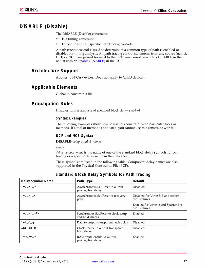
Chapter 4: Xilinx Constraints
DISABLE (Disable)The DISABLE (Disable) constraint:• Is a timing constraint.• Is used to turn off specific path tracing controls.
A path tracing control is used to determine if a common type of path is enabled ordisabled for timing analysis. All path tracing control statements from any source (netlist,UCF, or NCF) are passed forward to the PCF. You cannot override a DISABLE in thenetlist with an Enable (ENABLE) in the UCF.
Architecture SupportApplies to FPGA devices. Does not apply to CPLD devices.
Applicable ElementsGlobal in constraints file.
Propagation RulesDisables timing analysis of specified block delay symbol
Syntax ExamplesThe following examples show how to use this constraint with particular tools ormethods. If a tool or method is not listed, you cannot use this constraint with it.
UCF and NCF SyntaxDISABLE=delay_symbol_name;
wheredelay_symbol_name is the name of one of the standard block delay symbols for pathtracing or a specific delay name in the data sheet
These symbols are listed in the following table. Component delay names are alsosupported in the Physical Constraints File (PCF).
Standard Block Delay Symbols for Path TracingDelay Symbol Name Path Type Defaultreg_sr_o Asynchronous Set/Reset to output
propagation delayDisabled
reg_sr_r Asynchronous Set/Reset to recoverypath
Disabled for Virtex®-5 and earlierarchitectures
Enabled for Virtex-6 and Spartan®-6architectures
reg_sr_clk Synchronous Set/Reset to clock setupand hold checks
Enabled
lat_d_q Data to output transparent latch delay Disabled
lat_ce_q Clock Enable to output transparentlatch delay
Disabled
ram_we_o RAM write enable to outputpropagation delay
Enabled
Constraints GuideUG625 (v 12.3) September 21, 2010 www.xilinx.com 97
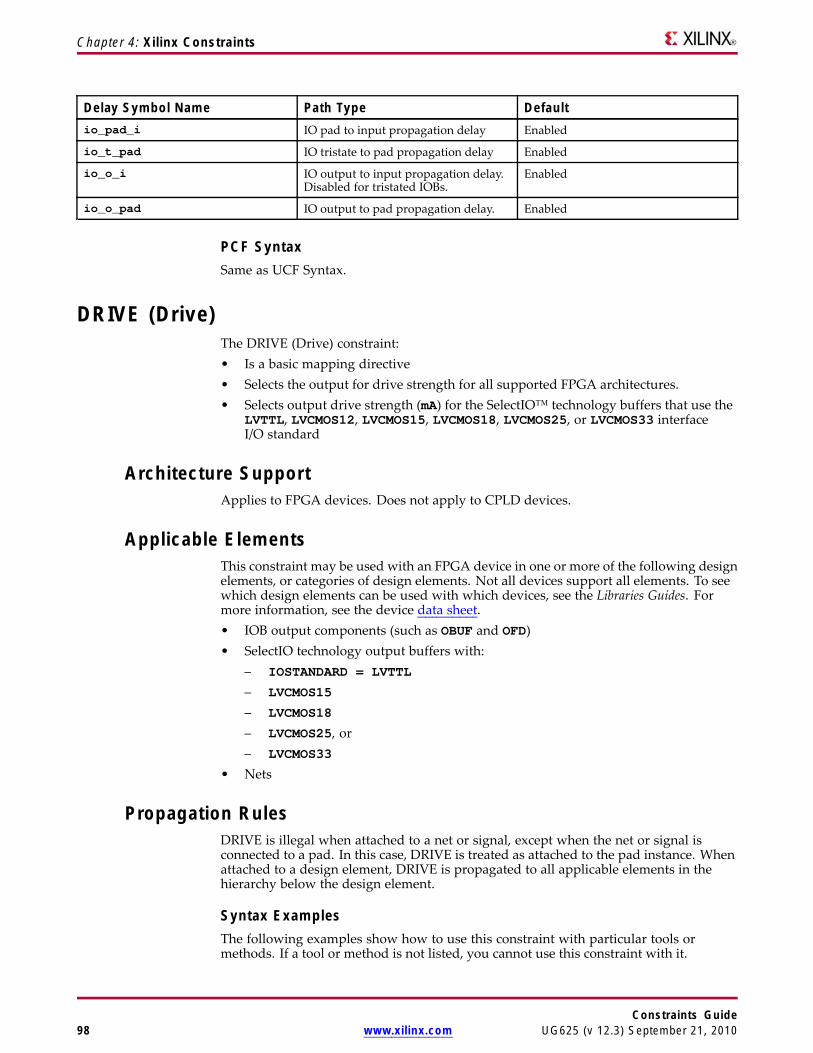
Chapter 4: Xilinx Constraints
Delay Symbol Name Path Type Defaultio_pad_i IO pad to input propagation delay Enabled
io_t_pad IO tristate to pad propagation delay Enabled
io_o_i IO output to input propagation delay.Disabled for tristated IOBs.
Enabled
io_o_pad IO output to pad propagation delay. Enabled
PCF SyntaxSame as UCF Syntax.
DRIVE (Drive)The DRIVE (Drive) constraint:• Is a basic mapping directive• Selects the output for drive strength for all supported FPGA architectures.• Selects output drive strength (mA) for the SelectIO™ technology buffers that use the
LVTTL, LVCMOS12, LVCMOS15, LVCMOS18, LVCMOS25, or LVCMOS33 interfaceI/O standard
Architecture SupportApplies to FPGA devices. Does not apply to CPLD devices.
Applicable ElementsThis constraint may be used with an FPGA device in one or more of the following designelements, or categories of design elements. Not all devices support all elements. To seewhich design elements can be used with which devices, see the Libraries Guides. Formore information, see the device data sheet.• IOB output components (such as OBUF and OFD)• SelectIO technology output buffers with:
– IOSTANDARD = LVTTL
– LVCMOS15
– LVCMOS18
– LVCMOS25, or– LVCMOS33
• Nets
Propagation RulesDRIVE is illegal when attached to a net or signal, except when the net or signal isconnected to a pad. In this case, DRIVE is treated as attached to the pad instance. Whenattached to a design element, DRIVE is propagated to all applicable elements in thehierarchy below the design element.
Syntax ExamplesThe following examples show how to use this constraint with particular tools ormethods. If a tool or method is not listed, you cannot use this constraint with it.
Constraints Guide98 www.xilinx.com UG625 (v 12.3) September 21, 2010

Chapter 4: Xilinx Constraints
Schematic Syntax• Attach to a valid IOB output component
• Attribute Name
DRIVE
• Attribute Values
For a list of the constraint values, see the UCF and NCF Syntax section below.
VHDL SyntaxDeclare the VHDL constraint as follows:
attribute drive: string;
Specify the VHDL constraint as follows:
attribute drive of {component_name |entity_name|label_name} : {component|entity|label} is “value”;
For a list of the constraint values, see the UCF and NCF Syntax section below.
For more information about basic VHDL syntax, see VHDL Attributes.
Verilog SyntaxPlace the Verilog constraint immediately before the module or instantiation.
Specify the Verilog constraint as follows:
(* DRIVE = “value” *)
For a list of the constraint values, see the UCF and NCF Syntax section below.
For more information about basic Verilog syntax, see Verilog Attributes.
UCF and NCF SyntaxThis section gives UCF and NCF Syntax examples for the following:
• IOB Output Components (UCF)
• SelectIO Technology Output Components
IOB Output Components (UCF)For Spartan®-3 and higher devices or Virtex®-4 and higher devices:
INST “instance_name” DRIVE={2|4|6| 8|12|16 |24};
12 mA is the default
SelectIO Technology Output ComponentsThis section applies to the following components:
• IOBUF_SelectIO• OBUF_SelectIO• OBUFT_SelectIO
The following table shows syntax examples for the named standard with Spartan-3devices and higher or Virtex-4 devices and higher. The default in each case is 12 mA.
Constraints GuideUG625 (v 12.3) September 21, 2010 www.xilinx.com 99

Chapter 4: Xilinx Constraints
Standard SyntaxLVTTL INST “instance_name” DRIVE={2|4|6|8|12|16|24};
LVCMOS12
LVCMOS15
LVCMOS18
INST “instance_name” DRIVE={2|4|6|8|12|16};
LVCMOS25
LVCMOS33
INST “instance_name” DRIVE={2|4|6|8|12|16|24};
XCF SyntaxMODEL “entity_name” drive={2|4|6|8|12|16|24};
BEGIN MODEL “entity_name ”
NET “signal_name” drive={2|4|6|8|12|16|24};
END;
PlanAhead™ SyntaxFor more information about using the PlanAhead™ software to create constraints, seeFloorplanning the Design in the PlanAhead User Guide. See PlanAhead in this Guide forinformation about:• Defining placement constraints• Assigning placement constraints• Defining I/O pin configurations• Floorplanning and placement constraints
DROP_SPEC (Drop Specifications)The DROP_SPEC (Drop Specifications) constraint:• Is an advanced timing constraint.• Allows you to specify that a timing constraint defined in the input design should
be dropped from the analysis.
Use DROP_SPEC when new specifications defined in a constraints file do not directlyoverride all specifications defined in the input design, and some of these input designspecifications need to be dropped. While this timing command is not expected to beused frequently in an input netlist or a Netlist Constraints File (NCF), it is legal. Ifdefined in an input design DROP_SPEC must be attached to TIMESPEC.
Architecture SupportApplies to all FPGA devices and all CPLD devices.
Applicable ElementsTiming constraints
Propagation RulesIt is illegal to attach this constraint to nets or macros. This constraint removes a specifiedtiming specification.
Constraints Guide100 www.xilinx.com UG625 (v 12.3) September 21, 2010

Chapter 4: Xilinx Constraints
Syntax ExamplesThe following examples show how to use this constraint with particular tools ormethods. If a tool or method is not listed, you cannot use this constraint with it.
UCF and NCF SyntaxTIMESPEC “TSidentifier”=DROP_SPEC;whereTSidentifier is the identifier name used for the timing specification to be removed
The following statement cancels the input design specification TS67.
TIMESPEC “TS67”=DROP_SPEC;
PCF Syntax“TSidentifier” DROP_SPEC;
ENABLE (Enable)The ENABLE (Enable) constraint:• Is a timing constraint.• Turns on specific path tracing controls.A path tracing control is used to determine if a common type of paths is enabled ordisabled for timing analysis. For more information, see Disable (DISABLE).
Architecture SupportApplies to FPGA devices. Does not apply to CPLD devices.
Applicable ElementsGlobal in constraints file
Propagation RulesEnables timing analysis for specified path delays.
Syntax ExamplesThe following examples show how to use this constraint with particular tools ormethods. If a tool or method is not listed, you cannot use this constraint with it.
UCF and NCF SyntaxENABLE can be applied only to a global timespec. The UCF path tracing syntax isas follows:
ENABLE= delay_symbol_name ;Where delay_symbol_name is the name of one of the standard block delay symbols forpath tracing symbols shown in the following table, or a specific delay name defined inthe data sheet
Constraints GuideUG625 (v 12.3) September 21, 2010 www.xilinx.com 101

Chapter 4: Xilinx Constraints
Standard Block Delay Symbols for Path TracingDelay Symbol Name Path Type Defaultreg_sr_o Asynchronous Set/Reset to output
propagation delayDisabled
reg_sr_r Asynchronous Set/Reset to recoverypath
Disabled for Virtex®-5 and earlierarchitectures
Enabled for Virtex-6 and Spartan®-6architectures
reg_sr_clk Synchronous Set/Reset to clock setupand hold checks
Enabled
lat_d_q Data to output transparent latch delay Disabled
lat_ce_q Clock Enable to output transparentlatch delay
Disabled
ram_we_o RAM write enable to outputpropagation delay
Enabled
io_pad_i IO pad to input propagation delay Enabled
io_t_pad IO tristate to pad propagation delay Enabled
io_o_1 IO output to input propagation delay.Disabled for tristated IOBs
Enabled
io_o_pad IO output to pad propagation delay Enabled
PCF SyntaxENABLE=delay_symbol_name ;
TIMEGRP name ENABLE=delay_symbol_name ;
ENABLE_SUSPEND (Enable Suspend)ENABLE_SUSPEND (Enable Suspend) defines the behavior of the SUSPENDpower-reduction mode for the Spartan®-3A device family.
Architecture SupportApplies to Spartan-3A and Spartan-6 devices only.
Applicable ElementsThis constraint is a global attribute for Spartan-3A devices and is not attached to anyparticular element.
Propagation RulesThis constraint is a global attribute that is attached to the entire design.
Syntax ExamplesThe following examples show how to use this constraint with particular tools ormethods. If a tool or method is not listed, you cannot use this constraint with it.
UCF SyntaxCONFIG ENABLE_SUSPEND=”{NO | FILTERED | UNFILTERED}”;
Constraints Guide102 www.xilinx.com UG625 (v 12.3) September 21, 2010

Chapter 4: Xilinx Constraints
ENABLE_SUSPEND values are:
• NO (default)
Disables this feature
• FILTERED
Activates the suspend feature with the glitch filter being activated (requires longerpulse width to activate)
• UNFILTERED
Activates the feature with the filter bypassed (quicker activation of SUSPEND)
UCF Syntax ExampleCONFIG ENABLE_SUSPEND=”FILTERED”;
FAST (Fast)The FAST (Fast) constraint:
• Is a basic mapping constraint.
• Increases the speed of an IOB output.
• May increase noise and power consumption.
Architecture SupportApplies to all FPGA devices and all CPLD devices.
Applicable Elements• Output primitives
• Output pads
• Bidirectional pads
You can also attach FAST to the net connected to the pad component in a UCF file.NGDBuild transfers the constraint from the net to the pad instance in the NGD file sothat it can be processed by the mapper. Use the following syntax:
NET “net_name” FAST;
Propagation RulesFAST is illegal when attached to a net except when the net is connected to a pad. In thisinstance, FAST is treated as attached to the pad instance. When attached to a macro,module, or entity, FAST is propagated to all applicable elements in the hierarchy belowthe module.
Syntax ExamplesThe following examples show how to use this constraint with particular tools ormethods. If a tool or method is not listed, you cannot use this constraint with it.
Constraints GuideUG625 (v 12.3) September 21, 2010 www.xilinx.com 103
Chapter 4: Xilinx Constraints
Schematic Syntax• Attach to a valid instance• Attribute Name
FAST
• Attribute Values– TRUE
– FALSE
VHDL SyntaxDeclare the VHDL constraint as follows:
attribute FAST: string;
Specify the VHDL constraint as follows:
attribute FAST of signal_name: signal is “{TRUE | FALSE}”;
For more information about basic VHDL syntax, see VHDL Attributes.
Verilog SyntaxPlace the Verilog constraint immediately before the module or instantiation.
Specify the Verilog constraint as follows:
(* FAST = “{TRUE | FALSE}” *)
For more information about basic Verilog syntax, see Verilog Attributes.
UCF and NCF SyntaxThe following statement increases the output speed of the element y2:
INST “$1I87/y2” FAST;
The following statement increases the output speed of the pad to which net1 isconnected:
NET “net1” FAST;
XCF SyntaxBEGIN MODEL “entity_name”
NET “signal_name” fast={TRUE | FALSE};
END;
PlanAhead™ SyntaxFor more information about using the PlanAhead™ software to create constraints, seeFloorplanning the Design in the PlanAhead User Guide. See PlanAhead in this Guide forinformation about:• Defining placement constraints• Assigning placement constraints• Defining I/O pin configurations• Floorplanning and placement constraints
Constraints Guide104 www.xilinx.com UG625 (v 12.3) September 21, 2010

Chapter 4: Xilinx Constraints
FEEDBACK (Feedback)The FEEDBACK (Feedback) constraint:• Is used to define the external DCM feedback path delay when the DCM is used in
board de-skew applications. The delay is defined as the maximum external pathdelay of the board trace and should not include any internal FPGA path delays.
• Is required for the timing tools to properly determine the DCM phase shift andanalyze the associated synchronous paths.
This constraint has the following values:
• input_feedback_clock_netThe name of the input pad net used as the feedback to the DCM
• valueThe board trace delay calculated or measured by you
• unitsns (default) or ps
• output_clock_netThe name of the output pad net driven by the DCM
Architecture SupportApplies to FPGA devices. Does not apply to CPLD devices.
Applicable ElementsNot applicable.
Propagation RulesBoth input_feedback_clock_net and output_clock_net must correspond to pad nets. Ifattached to any other net, an error results. The input_feedback_clock_netmust be an inputpad and output_clock_net must be an output pad.
Syntax ExamplesThe following examples show how to use this constraint with particular tools ormethods. If a tool or method is not listed, you cannot use this constraint with it.
UCF SyntaxNET output_clock_net FEEDBACK = valueunits NET input_feedback_clock_net ;
XCF SyntaxBEGIN MODEL “entity_name”
NET output_clock_net FEEDBACK = value units NET input_feedback_clock_net;
END;
PCF SyntaxBEL |COMP} output_clock_net FEEDBACK = value units {BEL |COMP}input_feedback_clock_net;{
Constraints GuideUG625 (v 12.3) September 21, 2010 www.xilinx.com 105

Chapter 4: Xilinx Constraints
Constraints Editor SyntaxFor information on Constraints Editor and Constraints Editor syntax in ISE® DesignSuite, see the ISE Design Suite Help.
PlanAhead™ SyntaxFor more information about using the PlanAhead™ software to create constraints, seeFloorplanning the Design in the PlanAhead User Guide. See PlanAhead in this Guide forinformation about:• Defining placement constraints• Assigning placement constraints• Defining I/O pin configurations• Floorplanning and placement constraints
FILE (File)When you instantiate a module that resides in another netlist, NGCBuild finds thisfile by looking it up by the file name. This requires the netlist to have the same nameas a module that is defined in the file. To name the netlist differently than the modulename, attach FILE (File) to an instance declaration. This tells NGCBuild to look forthe module in the file specified.
Some Xilinx® constraints cannot be used in attributes, because they are also VHDLkeywords. To avoid this problem, use a constraint alias. Each constraint has its ownalias. The alias name is based on the original constraint name with a XIL prefix. Forexample, FILE cannot be used in attributes directly. You must use XIL_FILE instead.The existing XILFILE alias is still supported.
Architecture SupportApplies to all FPGA devices and all CPLD devices.
Applicable ElementsInstance declaration where the definition is defined in the specified file.
Propagation RulesApplicable only on instances.
Syntax ExamplesThe following examples show how to use this constraint with particular tools ormethods. If a tool or method is not listed, you cannot use this constraint with it.
Schematic Syntax• Attach to a valid instance• Attribute Name
FILE
• Attribute Valuesfile_name.extension
Constraints Guide106 www.xilinx.com UG625 (v 12.3) September 21, 2010

Chapter 4: Xilinx Constraints
wherefile_name is the name of a file that represents the underlying logic for the elementcarrying the constraint.
Example file types include:• EDIF
• EDN
• NGC
• NMC
VHDL SyntaxDeclare the VHDL constraint as follows:
attribute xilfile: string;
Specify the VHDL constraint as follows:
attribute xilfile of {instance_name|component_name} : {label|component} is “file_name”;
For more information about basic VHDL syntax, see VHDL Attributes.
Verilog SyntaxPlace the Verilog constraint immediately before the module or instantiation.
Specify the Verilog constraint as follows:
(* XIL_FILE = "file_name" *)
For more information about basic Verilog syntax, see Verilog Attributes.
UCF and NCF SyntaxINST <instance definition> FILE= <filename definition is located in>;
No valid syntax for UCF.
FLOAT (Float)The FLOAT (Float) constraint:• Is a basic mapping constraint• Allows tristated pads to float when not being driven.This is useful when the default termination for applicable I/Os is set to any of thefollowing in ISE® Design Suite:• PULLUP
• PULLDOWN
• KEEPER
Architecture SupportApplies to CoolRunner™ XPLA3 and CoolRunner-II devices only.
Applicable ElementsApplies to nets or pins.
Constraints GuideUG625 (v 12.3) September 21, 2010 www.xilinx.com 107

Chapter 4: Xilinx Constraints
Propagation RulesApplies to the net or pin to which it is attached.
Syntax ExamplesThe following examples show how to use this constraint with particular tools ormethods. If a tool or method is not listed, you cannot use this constraint with it.
Schematic Syntax• Attach to a valid instance• Attribute Name
FLOAT
• Attribute Values– TRUE
– FALSE
– None required. If attached, TRUE is assumed.
VHDL SyntaxDeclare the VHDL constraint as follows:
attribute FLOAT: string;
Specify the VHDL constraint as follows:
attribute FLOAT of signal_name : signal is “{TRUE|FALSE}”;
Verilog SyntaxPlace this constraint immediately before an instantiation.
Specify the Verilog constraint as follows:
(* FLOAT = “{TRUE|FALSE}” *)
UCF and NCF SyntaxNET “signal_name ” FLOAT;
XCF SyntaxBEGIN MODEL “entity_name”
NET "signal_name" FLOAT;
END;
FROM-THRU-TO (From Thru To)The FROM-THRU-TO constraint:• Is an advanced timing constraint,• Is associated with the Period constraint of the high or low time.From synchronous paths, a FROM-TO-THRU constraint controls only the setup path,not the hold path. This constraint applies to a specific path that begins at a sourcegroup, passes through intermediate points, and ends at a destination group. The sourceand destination groups can be either user or predefined groups. You must define anintermediate path using TPTHRU before using THRU.
Constraints Guide108 www.xilinx.com UG625 (v 12.3) September 21, 2010

Chapter 4: Xilinx Constraints
Architecture SupportApplies to FPGA devices. Does not apply to CPLD devices.
Applicable ElementsPredefined and user-defined groups
Propagation RulesApplies to the specified FROM-THRU-TO path only.
Syntax ExamplesThe following examples show how to use this constraint with particular tools ormethods. If a tool or method is not listed, you cannot use this constraint with it.
UCF and NCF SyntaxTIMESPEC “TSidentifier”=FROM “source_group” THRU “thru_pt1”...[THRU “thru_pt2”...] TO “destination_group” value [Units] [DATAPATHONLY];
where• identifier can consist of characters or underbars• source_group and destination_group are user-defined or predefined groups• thru_pt1 and thru_pt2 are intermediate points to define specific paths for timing
analysis• value is the delay time• units can be ps, ms, ns, or micro
The DATAPATHONLY keyword indicates that the FROM-TO constraint does not takeclock skew or phase information into consideration. This keyword results in only thedata path between the groups being constrained and analyzed.
TIMESPEC TS_MY_PathB = FROM “my_src_grp” THRU “my_thru_pt” TO “my_dst_grp” 13.5 ns DATAPATHONLY;
FROM or TO is optional. You can have just a FROM or just a TO.
You are not required to have a FROM, THRU, or TO. You can have almost any combination,such as:• FROM-TO
• FROM-THRU-TO
• THRU-TO
• TO
• FROM
• FROM-THRU-THRU-THRU-TO
• FROM-THRU
There is no restriction on the number of THRU points. The source, THRU points, anddestination can be a net, bel, comp, macro, pin, or timegroup.
Constraints Editor SyntaxFor information on setting constraints in Constraints Editor, including syntax, see theConstraints Editor Help.
Constraints GuideUG625 (v 12.3) September 21, 2010 www.xilinx.com 109

Chapter 4: Xilinx Constraints
PlanAhead™ SyntaxFor more information about using the PlanAhead™ software to create constraints, seeFloorplanning the Design in the PlanAhead User Guide. See PlanAhead in this Guide forinformation about:• Defining placement constraints• Assigning placement constraints• Defining I/O pin configurations• Floorplanning and placement constraints
PCF SyntaxTSname=MAXDELAY FROM TIMEGRP "source" THRU TIMEGRP "thru_pt1" ...THRU"thru_ptn" TO TIMEGRP "destination" [DATAPATHONLY];
You are not required to have a FROM, THRU, and TO. You can have almostany combination (such as FROM-TO, FROM-THRU-TO, THRU-TO, TO, FROM,FROM-THRU-THRU-THRU-TO, and FROM-THRU). There is no restriction on thenumber of THRU points. The source, THRU points, and destination can be a net, bel,comp, macro, pin, or timegroup.
FROM-TO (From To)The FROM-TO (From To) constraint:• Defines a timing constraint between two groups.• Is associated with the Period constraint of the high or low time.A group can be user-defined or predefined. From synchronous paths, a FROM-TOconstraint controls only the setup path, not the hold path.
For Virtex®-5 devices, the FROM-TO constraint controls both setup and hold paths.
Architecture SupportApplies to all FPGA devices and all CPLD devices.
Applicable ElementsPredefined and user-defined groups.
Propagation RulesApplies to a path specified between two groups.
Syntax ExamplesThe following examples show how to use this constraint with particular tools ormethods. If a tool or method is not listed, you cannot use this constraint with it.
UCF and NCF SyntaxTIMESPEC TSname=FROM “group1” TO “group2” value [DATAPATHONLY];
Constraints Guide110 www.xilinx.com UG625 (v 12.3) September 21, 2010

Chapter 4: Xilinx Constraints
where
• TSname must always begin with TS. Any alphanumeric character or underscoremay follow.
• group1 is the origin path
• group2 is the destination path
• value is ns by default. Other possible values are MHz or another timing specificationsuch as TS_C2S/2 or TS_C2S*2.
The DATAPATHONLY keyword indicates that the FROM-TO constraint does not takeclock skew or phase information into consideration. This keyword results in only thedata path between the groups being constrained and analyzed.
TIMESPEC TS_MY_PathA = FROM “my_src_grp” TO “my_dst_grp” 23.5 nsDATAPATHONLY;
XCF SyntaxXST supports FROM-TO with the following limitations:
• FROM-THRU-TO is not supported
• Linked Specification is not supported
• Pattern matching for predefined groups is not supported:
TIMESPEC TS_1 = FROM FFS(machine/*) TO FFS 2 ns;
Constraints Editor SyntaxFor information on setting constraints in Constraints Editor, including syntax, see theConstraints Editor Help.
PlanAhead™ SyntaxFor more information about using the PlanAhead™ software to create constraints, seeFloorplanning the Design in the PlanAhead User Guide. See PlanAhead in this Guide forinformation about:
• Defining placement constraints
• Assigning placement constraints
• Defining I/O pin configurations
• Floorplanning and placement constraints
PCF SyntaxTSname=MAXDELAY FROM TIMEGRP "group1" TO TIMEGRP "group2" value[DATAPATHONLY];
Constraints GuideUG625 (v 12.3) September 21, 2010 www.xilinx.com 111
Chapter 4: Xilinx Constraints
You are not required to have a FROM, THRU, and TO. You can have almost anycombination, such as:• FROM-TO• FROM-THRU-TO• THRU-TO• TO• FROM• FROM-THRU-THRU-THRU-TO• FROM-THRUThere is no restriction on the number of THRU points. The source, THRU points, anddestination can be any of the following:• net• bel• comp• macro• pin• timegroup
FSM_STYLE (FSM Style)For information about the FSM_STYLE (FSM Style) constraint, see the XST User Guideand the XST User Guide for Virtex-6 and Spartan-6 Devices.
HBLKNM (Hierarchical Block Name)The HBLKNM (Hierarchical Block Name) constraint:• Is an advanced mapping constraint.• Assigns hierarchical block names to logic elements and controls grouping in a
flattened hierarchical design. When elements on different levels of a hierarchicaldesign carry the same block name, and the design is flattened, NGCBuild prefixes ahierarchical path name to the HBLKNM value.
Like Block Name, HBLKNM forces function generators and flip-flops into the same CLB.Symbols with the same HBLKNM constraint map into the same CLB, if possible.
However, using HBLKNM instead of Block Name has the advantage of adding hierarchypath names during translation, and therefore the same HBLKNM constraint and valuecan be used on elements within different instances of the same design element.
Architecture SupportApplies to FPGA devices. Does not apply to CPLD devices.
Applicable ElementsHBLKNM may be used with an FPGA device in one or more of the following designelements, or categories of design elements. Not all devices support all elements. To seewhich design elements can be used with which device families, see the Xilinx® LibrariesGuides for details. For more information, see the device data sheet.
Constraints Guide112 www.xilinx.com UG625 (v 12.3) September 21, 2010

Chapter 4: Xilinx Constraints
This constraint may be used with an FPGA device in one or more of the following designelements, or categories of design elements. Not all devices support all elements. To seewhich design elements can be used with which devices, see the Libraries Guides. Formore information, see the device data sheet.• Registers
• I/O elements and pads
• FMAP
• PULLUP
• ACLK
• GCLK
• BUFG
• BUFGS
• BUFGP
• ROM
• RAMS
• RAMD
• Carry logic primitives
You can also attach HBLKNM to the net connected to the pad component in a UCF file.NGCBuild transfers the constraint from the net to the pad instance in the NGD file sothat it can be processed by the mapper. Use the following syntax:
NET “net_name” HBLKNM=property_value;
Propagation RulesWhen attached to a design element, HBLKNM is propagated to all applicable elementsin the hierarchy within the design element. However, when attached to a NET,HBLKNM is only propagated to PADs.
SyntaxThe following examples show how to use this constraint with particular tools ormethods. If a tool or method is not listed, you cannot use this constraint with it.
Schematic Syntax• Attach to a valid instance• Attribute Name
HBLKNM• Attribute Values
block_name
VHDL SyntaxDeclare the VHDL constraint as follows:
attribute hblknm: string;
Specify the VHDL constraint as follows:
attribute hblknm of {entity_name|component_name|signal_name|label_name}:{entity|component|signal|label} is “block_name”;
whereblock_name is a valid block name for that type of symbol
Constraints GuideUG625 (v 12.3) September 21, 2010 www.xilinx.com 113

Chapter 4: Xilinx Constraints
For more information about basic VHDL syntax, see VHDL Attributes.
Verilog SyntaxPlace the Verilog constraint immediately before the module or instantiation.
Specify the Verilog constraint as follows:
(* HBLKNM = “block_name” *)block_name is a valid block name for that type of symbol
For more information about basic Verilog syntax, see Verilog Attributes.
UCF and NCF SyntaxNET “net_name” HBLKNM=property_value;
INST “instance_name” HBLKNM=block_name;block_name is a valid block name for that type of symbol
The following statement specifies that the element this_fmap is put into the block namedgroup1.
INST “$I13245/this_fmap” HBLKNM=group1;
The following statement attaches HBLKNM to the pad connected to net1.
NET “net1” HBLKNM=$COMP_0;
Elements with the same HBLKNM are placed in the same logic block if possible.Otherwise an error occurs. Conversely, elements with different block names are notput into the same block.
HIODELAY_GROUP (HIODELAY Group)The HIODELAY_GROUP (HIODELAY Group) constraint:• Is a design implementation constraint.• Groups a hierarchical set of IDELAY and IODELAYs with an IDELAYCTRL to enable
automatic replication and placement of IDELAYCTRL in a design.For more information, see the IDELAYCTRL section of the device user guide.
Architecture SupportApplies to Virtex®-4 and Virtex-5 devices. For Virtex-4 devices, HIODELAY_GROUP issupported only when using the Timing Driven Pack and Placement Option in MAP.
Applicable ElementsIDELAY, IODELAY, and IDELAYCTRL primitive instantiations
Propagation RulesHIODELAY_GROUP can be attached only to a design element. It is illegal to attachHIODELAY_GROUP to a net, signal, or pin. To merge two or more embeddedHIODELAY_GROUP constraints in your design, see MIODELAY_GROUP (MIODELAYGroup).
Constraints Guide114 www.xilinx.com UG625 (v 12.3) September 21, 2010

Chapter 4: Xilinx Constraints
Syntax ExamplesThe following examples show how to use this constraint with particular tools ormethods. If a tool or method is not listed, you cannot use this constraint with it.
VHDL SyntaxDeclare the VHDL constraint as follows:
attribute HIODELAY_GROUP: string;
Specify the VHDL constraint as follows:
attribute HIODELAY_GROUP of {component_name|label_name}: {component|label} is"group_name";
For a description of group_name, see UCF and NCF Syntax below.
For more information about basic VHDL syntax, see VHDL Attributes.
Verilog SyntaxPlace the Verilog constraint immediately before the module or instantiation.
Specify the Verilog constraint as follows:
(* HIODELAY_GROUP = "group_name" *)
For a description of group_name, see UCF and NCF Syntax below.
For more information about basic Verilog syntax, see Verilog Attributes.
UCF and NCF SyntaxINST "instance_name" HIODELAY_GROUP = group_name;
where
group_name is the name assigned to a set of IDELAY or IODELAY constraints and anIDELAYCTRL to uniquely define the group.
Hierarchical Lookup Table Name (HLUTNM)The Hierarchical Lookup Table Name (HLUTNM) constraint:
• Allows you to control the grouping of logical symbols into the LUT sites of theVirtex®-5 FPGA architectures.
• Is a string value property that is applied to two qualified symbols.
• Must be applied uniquely to two symbols within a given level of hierarchy. Thesetwo symbols are implemented in a shared LUT site within a SLICE component.
• Is functionally similar to HBLKNM (Hierarchical Block Name)
Architecture SupportApplies to Virtex-5 devices only.
Constraints GuideUG625 (v 12.3) September 21, 2010 www.xilinx.com 115

Chapter 4: Xilinx Constraints
HLUTNM Applicable ElementsHLUTNM can be applied to:• Two symbols that:
– Share a common hierarchy, and– Are unique within their level of hierarchy
• Two 5-input or smaller function generator symbols (LUT, SRL16) if the total numberof unique input pins required for both symbols does not exceed 5 pins.
• A 6-input read-only function generator symbol (LUT6) in conjunction with a 5-inputread-only symbol (LUT5) if:– The total number of unique input pins required for both symbols does not
exceed 6 inputs, and– The lower 32 bits of the 6-input symbol programming matches all 32 bits of the
5-input symbol programming.
Propagation RulesCan be applied to two symbols that share a common hierarchy and that are also uniquewithin their level of hierarchy.
Syntax ExamplesThe following examples show how to use this constraint with particular tools ormethods. If a tool or method is not listed, you cannot use this constraint with it.
Schematic Syntax• Attach to a valid element or symbol type• Attribute Name
HLUTNM
• Attribute Value<user_defined>
VHDL SyntaxDeclare the VHDL constraint as follows:
attribute hlutnm: string;
Specify the VHDL constraint as follows:
attribute hlutnm of instance_name : label is “string_value ”;
where• instance_name is the instance name of an instantiated LUT, or LUTRAM.• string_value is applied uniquely to two symbols within a given level of hierarchy.
– There is no default value.– If the value is blank, the constraint is ignored.
For more information about basic VHDL syntax, see VHDL Attributes.
Verilog SyntaxPlace the Verilog constraint immediately before the module or instantiation.
Specify the Verilog constraint as follows:
(* HLUTNM = “string_value” *)
Constraints Guide116 www.xilinx.com UG625 (v 12.3) September 21, 2010
Chapter 4: Xilinx Constraints
where• string_value is applied uniquely to two symbols within a given level of hierarchy.• There is no default value.• If the value is blank, the constraint is ignored.
For more information about basic Verilog syntax, see Verilog Attributes.
UCF and NCF SyntaxINST “symbol_name” HLUTNM=string_value ;
where• string_value is applied uniquely to two symbols within a given level of hierarchy.• There is no default value.• If the value is blank, the constraint is ignored.
XCF SyntaxMODEL “symbol_name” hlutnm = string_value ;
where• string_value is applied uniquely to two symbols within a given level of hierarchy.• There is no default value.• If the value is blank, the constraint is ignored.
H_SET (H Set)See HU_SET (HU Set).
HU_SET (HU Set)The HU_SET (HU Set) constraint:• Is an advanced mapping constraint.• Is defined by the design hierarchy.• Allows you to specify a set name.
Note It is possible to have only one H_SET within a given hierarchical element, butby specifying set names, you can specify several HU_SET sets.
NGCBuild hierarchically qualifies the name of the HU_SET as it flattens the design andattaches the hierarchical names as prefixes.
Differences Between HU_SET and H_SETHU_SET H_SETHas an explicit user-defined and hierarchically qualifiedname for the set
Has only an implicit hierarchically qualified name generatedby the design-flattening program
Starts with the symbols that are assigned the HU_SETconstraint
Starts with the instantiating macro one level above thesymbols with the RLOC constraints
For more information about set attributes, see Relative Location (RLOC).
Architecture SupportApplies to FPGA devices. Does not apply to CPLD devices.
Constraints GuideUG625 (v 12.3) September 21, 2010 www.xilinx.com 117

Chapter 4: Xilinx Constraints
Applicable ElementsThis constraint may be used with an FPGA device in one or more of the following designelements, or categories of design elements. Not all devices support all elements. To seewhich design elements can be used with which devices, see the Libraries Guides. Formore information, see the device data sheet.• Registers• FMAP• Macro Instance• ROM• RAMS, RAMD• MULT18X18S• RAMB4_Sm_Sn, RAMB4_Sn• RAMB16_Sm_Sn, RAMB16_Sn• RAMB16• DSP48
Propagation RulesThis constraint is a design element constraint. Any attachment to a net is illegal.
Syntax ExamplesThe following examples show how to use this constraint with particular tools ormethods. If a tool or method is not listed, you cannot use this constraint with it.
Schematic Syntax• Attach to a valid instance• Attribute Name
HU_SET
• Attribute Valuesset_name
VHDL SyntaxDeclare the VHDL constraint as follows:
attribute HU_SET: string;
Specify the VHDL constraint as follows:
attribute HU_SET of {component_name | entity_name | label_name} : {component | entity| label} is "set_name";
For more information about basic VHDL syntax, see VHDL Attributes.
Verilog SyntaxPlace the Verilog constraint immediately before the module or instantiation.
Specify the Verilog constraint as follows:
(* HU_SET = "set_name" *)
For more information about basic Verilog syntax, see Verilog Attributes.
Constraints Guide118 www.xilinx.com UG625 (v 12.3) September 21, 2010

Chapter 4: Xilinx Constraints
UCF and NCF SyntaxINST "instance_name" HU_SET=set_name ;
where• set_name is the identifier for the set• set_name must be unique among all the sets in the design
The following statement assigns an instance of the register FF_1 to a set namedheavy_set.
INST "$1I3245/FF_1" HU_SET=heavy_set;
XCF SyntaxMODEL "entity_name" hu_set={yes | no};
BEGIN MODEL "entity_name"
INST "instance_name" hu_set=yes;
END;
IBUF_DELAY_VALUE (Input Buffer Delay Value)The IBUF_DELAY_VALUE (Input Buffer Delay Value) constraint:• Is a mapping constraint.• Adds additional static delay to the input path of the FPGA array.• Can be applied to any input or bi-directional signal that is not directly driving a
clock or IOB (Input Output Block) register.For more information regarding the constraint of signals driving clock and IOB registers,see IFD_DELAY_VALUE. IBUF_DELAY_VALUE can be set to an integer value from0-16. The value 0 is the default value, and applies no additional delay to the inputpath. A larger value correlates to a larger delay added to input path. These values donot directly correlate to a unit of time but rather additional buffer delay. For moreinformation, see the device data sheets.
Architecture SupportApplies to Spartan®-3A and Spartan-3E devices.
Applicable ElementsAny top-level I/O port.
Syntax ExamplesThe following examples show how to use this constraint with particular tools ormethods. If a tool or method is not listed, you cannot use this constraint with it.
Schematic Syntax• Attach a new property to the top-level port of the schematic• Attribute Name
IBUF_DELAY_VALUE
• Attribute Values0-16
Constraints GuideUG625 (v 12.3) September 21, 2010 www.xilinx.com 119
Chapter 4: Xilinx Constraints
VHDL SyntaxAttach a VHDL attribute to the appropriate top-level port.
attribute IBUF_DELAY_VALUE : string;
attribute IBUF_DELAY_VALUE of top_level_port_name: signal is "value";
a valid value is from 0 to 16.
The following statement assigns an IBUF_DELAY_VALUE increment of 5 to the netDataIn1
attribute IBUF_DELAY_VALUE : string;
attribute IBUF_DELAY_VALUE of DataIn1: label is "5";
For more information about basic VHDL syntax, see VHDL Attributes.
Verilog SyntaxAttach a Verilog attribute to the appropriate top-level port.
(* IBUF_DELAY_VALUE="value" *) input top_level_port_name;
where
A valid value is from 0 to 16.
The following statement assigns an IBUF_DELAY_VALUE increment of 5 to the netDataIn1.
(* IBUF_DELAY_VALUE="5" *) input DataIn1;
For more information about basic Verilog syntax, see Verilog Attributes.
UCF and NCF SyntaxNET "top_level_port_name" IBUF_DELAY_VALUE = value;
where
• value is the numerical IBUF delay setting.
• A valid value is from 0 to 16.
The following statement assigns an IBUF_DELAY_VALUE increment of 5 to the netDataIn1.
NET "DataIn1" IBUF_DELAY_VALUE = 5;
Constraints Guide120 www.xilinx.com UG625 (v 12.3) September 21, 2010
Chapter 4: Xilinx Constraints
IFD_DELAY_VALUE (IFD Delay Value)The IFD_DELAY_VALUE (IFD Delay Value) constraint:• Is a mapping constraint.• Adds additional static delay to the input path of the FPGA array.• Can be applied to any input or bi-directional signal which drives an IOB (Input
Output Block) register.For more information on the constraint of signals which do not drive IOB registers,see Input Buffer Delay Value (IBUF_DELAY_VALUE).
• Can be set to– an integer value from 0-8– AUTO
AUTO is the default value, and is used to guarantee that the input hold time ofthe destination register is met by automatically adding the appropriate amountof delay to the data path.
When IFD_DELAY_VALUE is set to 0, the data path has no additional delay added. Theintegers 1-8 correspond to increasing amounts of delay added to the data path. Thesevalues do not directly correlate to a unit of time but rather additional buffer delay. Formore information, see the device data sheets.
Architecture SupportSupports Spartan®-3A and Spartan-3E devices.
Applicable ElementsAny top-level I/O port
Propagation RulesAlthough IFD_DELAY_VALUE is attached to an I/O symbol, it applies to the entireI/O component.
Syntax ExamplesThe following examples show how to use this constraint with particular tools ormethods. If a tool or method is not listed, you cannot use this constraint with it.
Schematic Syntax• Attach to a net• Attribute Name
IFD_DELAY_VALUE
• Attribute Values– 0-8
– AUTO
VHDL SyntaxAttach a VHDL attribute to the appropriate top-level port.
attribute IFD_DELAY_VALUE : string;
Constraints GuideUG625 (v 12.3) September 21, 2010 www.xilinx.com 121

Chapter 4: Xilinx Constraints
The following statement assigns an IFD_DELAY_VALUE increment of 5 to the netDataIn1:
attribute IFD_DELAY_VALUE : string;
attribute IFD_DELAY_VALUE of DataIn1: label is "5";
Verilog SyntaxAttach a Verilog attribute to the appropriate top-level port.
(* IFD_DELAY_VALUE="value" *) input top_level_port_name;
The following statement assigns an IFD_DELAY_VALUE increment of 5 to the netDataIn1:
(* IFD_DELAY_VALUE="5" *) input DataIn1;
UCF and NCF SyntaxNET "top_level_port_name" IFD_DELAY_VALUE = value;value is the numerical IBUF delay setting
The following statement assigns an IFD_DELAY_VALUE increment of 5 to the netDataIn1:
NET "DataIn1" IFD_DELAY_VALUE = 5;
IN_TERM (In Term)The IN_TERM (In Term) constraint:• Is a basic mapping constraint.• Sets a configuration of input termination resistors .In Term is valid on an input pad NET, input pad INST, or for the entire design.
Architecture SupportApplies to FPGA devices. Does not apply to CPLD devices.
Applicable ElementsThis constraint may be used with an FPGA device in one or more of the following designelements, or categories of design elements:• IOB input components (such as IBUF)• Input Pad NetNot all devices support all elements. To see which design elements can be used withwhich devices, see the Libraries Guides. For more information, see the device data sheet.
Propagation RulesIN_TERM is illegal when attached to a net or signal, except when the net or signal isconnected to a pad. In this case, IN_TERM is treated as attached to the pad instance.
Syntax ExamplesThe following examples show how to use this constraint with particular tools ormethods. If a tool or method is not listed, you cannot use this constraint with it.
Constraints Guide122 www.xilinx.com UG625 (v 12.3) September 21, 2010
Chapter 4: Xilinx Constraints
ValuesThis constraint has the following values:
• NONE• TUNED_SPLIT• UNTUNED_SPLIT_25• UNTUNED_SPLIT_50• UNTUNED_SPLIT_75
Schematic Syntax• Attach to a pad net• Attribute Name
IN_TERM• Attribute Values
See Values section above.
VHDL SyntaxDeclare the VHDL constraint as follows:
Attribute IN_TERM: string;
Specify the VHDL constraint as follows:
attribute IN_TERM of signal_name: signal is “{NONE | TUNED_SPLIT |UNTUNED_SPLIT_25 | UNTUNED_SPLIT_50 | UNTUNED_SPLIT_75}”;
For more information about basic VHDL syntax, see VHDL Attributes.
Verilog SyntaxPlace the Verilog constraint immediately before the module or instantiation.
Specify the Verilog constraint as follows:
(* IN_TERM = “{NONE | TUNED_SPLIT | UNTUNED_SPLIT_25 |UNTUNED_SPLIT_50 | UNTUNED_SPLIT_75 }” *)
For more information about basic Verilog syntax, see Verilog Attributes.
UCF and NCF SyntaxThe following statement configures the IO to use a PULLUP.
NET "pad_net_name"IN_TERM = “{NONE | TUNED_SPLIT | UNTUNED_SPLIT_25| UNTUNED_SPLIT_50 | UNTUNED_SPLIT_75 }” ;
The following statement configures IN_TERM to be used globally.
DEFAULT IN_TERM = TUNED_SPLIT;
XCF SyntaxBEGIN MODEL “entity_name”
NET "signal_name" in_term=tuned_split;
END;
Constraints GuideUG625 (v 12.3) September 21, 2010 www.xilinx.com 123

Chapter 4: Xilinx Constraints
PlanAhead™ SyntaxFor more information about using the PlanAhead™ software to create constraints, seeFloorplanning the Design in the PlanAhead User Guide. See PlanAhead in this Guide forinformation about:• Defining placement constraints• Assigning placement constraints• Defining I/O pin configurations• Floorplanning and placement constraints
INREG (Input Registers)INREG (Input Registers) applies to register and latch instances with their D-inputsdriven by input pads, or to the Q-output nets of such registers and latches. By default,registers and latches for CoolRunner™ XPLA3 and CoolRunner-II designs that havetheir D-inputs driven by input pads are automatically implemented using the device’sFast Input path, where possible. If you disable the ISE® Design Suite property Use FastInput for INREG for the Fit (Implement Design) process, then only register and latcheswith the INREG attribute are considered for Fast Input optimization.
Architecture SupportApplies to CoolRunner™ XPLA3 and CoolRunner-II devices only.
Applicable ElementsApplies to register and latch instances with their D-inputs driven by input pads or to theQ-output nets of such registers or latches.
Propagation RulesApplies to register or latch to which it is attached or to the Q-output nets of suchregisters or latches
Syntax ExcamplesThe following examples show how to use this constraint with particular tools ormethods. If a tool or method is not listed, you cannot use this constraint with it.
Schematic Syntax• Attach to a register, latch, or net• Attribute Name
INREG
• Attribute ValuesNone (TRUE by default)
UCF SyntaxNET “signal_name” INREG;
INST “register_name” INREG;
Constraints Guide124 www.xilinx.com UG625 (v 12.3) September 21, 2010

Chapter 4: Xilinx Constraints
Internal Vref Bank (INTERNAL_VREF_BANK)The Internal Vref Bank (INTERNAL_VREF_BANK) constraint:• Provides a means of assigning a voltage value to the internal Vref feature for a
given IO bank.• Is useful for freeing the Vref pins of IO banks from their function of providing
a voltage reference. By using the internal Vref on an IO bank, the Vref pins canassume an alternative use.
Architecture SupportVirtex®-6
Applicable ElementsThis constraint is a global CONFIG constraint and is not attached to any instance orsignal name.
Propagation RulesApplies to IOs in the specified bank for the entire design
Syntax ExamplesThe following examples show how to use this constraint with particular tools ormethods. If a tool or method is not listed, you cannot use this constraint with it.
UCF and NCF SyntaxCONFIG INTERNAL_VREF_BANKn=v;
where• n is the number of the bank• v is the target voltage value (0.0, 0.6, 0.75, 0.9, 1.1, 1.25)
ExampleCONFIG INTERNAL_VREF_BANK5=1.1;
IOB (IOB)The IOB constraint:• Is a basic mapping and synthesis constraint.• Indicates which flip-flops and latches can be moved into the IOB/ILOGIC/OLOGIC.The mapper supports a command line option (-pr i | o | b | off) that allows flip-flopor latch primitives to be pushed into the input IOB (i), output IOB (o), or input/outputIOB (b) on a global scale. The IOB constraint, when associated with a flip-flop or latch,tells the mapper to pack that instance into an IOB type component if possible. The IOBconstraint has precedence over the mapper -pr command line option. However, IOBconstraints do not have precedence over LOC constraints.
XST considers the IOB constraint as an implementation constraint, and thereforepropagates it in the generated NGC file. XST also duplicates the flip-flops and latchesdriving the Enable pin of output buffers, so that the corresponding flip-flops and latchescan be packed in the IOB.
Constraints GuideUG625 (v 12.3) September 21, 2010 www.xilinx.com 125

Chapter 4: Xilinx Constraints
This constraint has the following values:
• TRUE
Allows the flip-flop or latch to be pulled into an IOB• FALSE
Indicates not to pull it into an IOB• AUTO
Used by XST only. XST takes into account timing constraints and automaticallydecides to push or not to push flip-flops into IOBs
• FORCE
Requires that the flip-flop or latch be pulled into an IOB, otherwise an error isgiven. FORCE produces an error only if the register has I/O connections and cannotbe packed in the IOB.
Architecture SupportApplies to FPGA devices. Does not apply to CPLD devices.
Applicable Elements• Non-INFF/OUTFF flip-flop and latch primitives• Registers
Propagation RulesApplies to the design element to which it is attached.
Syntax ExamplesThe following examples show how to use this constraint with particular tools ormethods. If a tool or method is not listed, you cannot use this constraint with it.
Schematic Syntax• Attach to a flip-flop or latch instance or to a register• Attribute Name
IOB
VHDL SyntaxDeclare the VHDL constraint as follows:
attribute iob: string;
Specify the VHDL constraint as follows:
attribute iob of {component_name |entity_name|label_name|signal_name} :{component|entity |label|signal} is "{TRUE|FALSE|AUTO|FORCE}";
For more information about basic VHDL syntax, see VHDL Attributes.
Verilog SyntaxPlace the Verilog constraint immediately before the module or instantiation.
Specify the Verilog constraint as follows:
(* IOB = "{TRUE|FALSE |AUTO|FORCE}" *)
Constraints Guide126 www.xilinx.com UG625 (v 12.3) September 21, 2010

Chapter 4: Xilinx Constraints
For more information about basic Verilog syntax, see Verilog Attributes.
UCF and NCF SyntaxINST "instance_name" IOB={TRUE|FALSE|FORCE};
The following statement instructs the mapper to place the foo/bar instance into an IOBcomponent.
INST "foo/bar" IOB=TRUE;
XCF SyntaxBEGIN MODEL "entity_name"
NET "signal_name" iob={true|false|auto|force};
INST " instance_name" iob={true |false |auto|force};
END;
For the AUTO option, XST takes into account timing constraints and automaticallydecides to push or not to push flip-flops into IOBs
Constraints Editor SyntaxFor information on setting constraints in Constraints Editor, including syntax, see theConstraints Editor Help.
IOBDELAY (Input Output Block Delay)The IOBDELAY (Input Output Block Delay) constraint:• Is a basic mapping constraint.• Specifies how the input path delay elements in all devices are to be programmed.
There are two possible destinations for input signals:• The local IOB input FF• A load external to the IOBXilinx® devices allow a delay element to delay the signal going to one or both of thesedestinations.
IOBDELAY cannot be used concurrently with No Delay (NODELAY).
This constraint has the following values:
• NONE sets the delay OFF for both the IBUF and IFD paths.– The following statement sets the delay OFF for the IBUF and IFD paths.
INST “xyzzy” IOBDELAY=NONE– For Spartan®-3 devices, the default is not set to NONE so the device can achieve
a zero hold time.• BOTH sets the delay ON for both the IBUF and IFD paths.• IBUF sets the delay to OFF for any register inside the I/O component and to ON for
the registers outside of the component if the input buffer drives a register D pinoutside of the I/O component.
• IFD sets the delay to ON for any register inside the I/O component and to OFF forthe registers outside the component if a register occupies the input side of the I/Ocomponent, regardless of whether the register has the IOB=TRUE constraint.
Constraints GuideUG625 (v 12.3) September 21, 2010 www.xilinx.com 127
Chapter 4: Xilinx Constraints
Architecture SupportApplies to FPGA devices. Does not apply to CPLD devices.
Applicable ElementsAny I/O symbol (I/O pads, I/O buffers, or input pad nets)
Propagation RulesAlthough IOBDELAY is attached to an I/O symbol, it applies to the entire I/O component.
Syntax ExamplesThe following examples show how to use this constraint with particular tools ormethods. If a tool or method is not listed, you cannot use this constraint with it.
Schematic Syntax• Attach to an I/O symbol• Attribute Name: IOBDELAY
VHDL SyntaxDeclare the VHDL constraint as follows:
attribute iobdelay: string;
Specify the VHDL constraint as follows:
attribute iobdelay of {component_name |label_name}: {component|label} is“{NONE|BOTH|IBUF|IFD}”;
For more information about basic VHDL syntax, see VHDL Attributes.
Verilog SyntaxPlace the Verilog constraint immediately before the module or instantiation.
Specify the Verilog constraint as follows:
(* IOBDELAY = {NONE|BOTH|IBUF|IFD} *)
For more information on basic Verilog syntax, see Verilog Attributes.
UCF and NCF SyntaxINST “ instance_name” IOBDELAY={NONE|BOTH|IBUF|IFD};
IODELAY_GROUP (IODELAY Group)The IODELAY_GROUP (IODELAY Group) constraint:• Is a design implementation constraint.• Groups a set of IDELAY and IODELAYs with an IDELAYCTRL to enable automatic
replication and placement of IDELAYCTRL in a design.For more information, see the IDELAYCTRL section of the device user guide.
Architecture SupportApplies to Virtex®-4 and Virtex-5 devices. For Virtex-4 devices, IODELAY_GROUP issupported only when using the Timing Driven Pack and Placement Option in MAP.
Constraints Guide128 www.xilinx.com UG625 (v 12.3) September 21, 2010

Chapter 4: Xilinx Constraints
Applicable ElementsIDELAY, IODELAY, and IDELAYCTRL primitive instantiations.
Propagation RulesIODELAY_GROUP can only be attached to a design element. It is illegal to attachIODELAY_GROUP to a net, signal, or pin. To merge two or more embeddedIODELAY_GROUP constraints in your design, see MIODELAY_GROUP.
Syntax ExamplesThe following examples show how to use this constraint with particular tools ormethods. If a tool or method is not listed, you cannot use this constraint with it.
VHDL SyntaxDeclare the VHDL constraint as follows:
attribute IODELAY_GROUP: string;
Specify the VHDL constraint as follows:
attribute IODELAY_GROUP of {component_name|label_name}: {component|label} is"group_name";
For a description of group_name, see the UCF Syntax for this constraint.
For more information about basic VHDL syntax, see VHDL Attributes.
Verilog SyntaxPlace the Verilog constraint immediately before the module or instantiation.
Specify the Verilog constraint as follows:
(* IODELAY_GROUP = "group_name" *)
For a description of group_name, see UCF Syntax below.
For more information about basic Verilog syntax, see Verilog Attributes.
UCF SyntaxINST "instance_name" IODELAY_GROUP = group_name;
where
group_name is the name assigned to a set of IDELAY or IODELAY constraints and anIDELAYCTRL to uniquely define the group.
IOSTANDARD (Input Output Standard)The IOSTANDARD (Input Output Standard) constraint:• Is a basic mapping constraint.• Is a synthesis constraint.
IOSTANDARD for FPGA DevicesUse IOSTANDARD to assign an I/O standard to an I/O primitive.
Constraints GuideUG625 (v 12.3) September 21, 2010 www.xilinx.com 129
Chapter 4: Xilinx Constraints
All components with IOSTANDARD must follow the same placement rules (bankingrules) as the SelectIO™ components. See the Xilinx® Libraries Guides for information onthe banking rules for each architecture. For descriptions of the supported I/O standards,see the device data sheet.
For Spartan®-3, Spartan-3A, Spartan-3E, Virtex®-4, and Virtex-5 devices, therecommended procedure is to attach IOSTANDARD to a buffer component insteadof using the SelectIO variants of a component. For example, use an IBUF with theIOSTANDARD=HSTL_III constraint instead of the IBUF_HSTL_III component.
For Spartan-3, Spartan-3A, Spartan-3E, Virtex-4, and Virtex-5 devices, differentialsignaling standards apply to IBUFDS, IBUFGDS, OBUFDS, and OBUFTDS only (notIBUF or OBUF).
IOSTANDARD for CPLD DevicesYou can apply IOSTANDARD to I/O pads of CoolRunner™-II devices to specify bothinput threshold and output VCCIO voltage. For supported values, see the device datasheet.
The CPLD fitter automatically groups outputs with compatible IOSTANDARD settingsinto the same bank when no location constraints are specified.
Architecture SupportApplies to all FPGA devices and CoolRunner-II CPLD devices.
Applicable ElementsTo see which design elements can be used with which device families, see the LibrariesGuides. For more information, see the device data sheet.• IBUF, IBUFG, OBUF, OBUFT• IBUFDS, IBUFGDS, OBUFDS, OBUFTDS• Output Voltage Banks
Propagation RulesIt is illegal to attach IOSTANDARD to a net or signal except when the signal or net isconnected to a pad. In this case, IOSTANDARD is treated as attached to an IOB instance(IBUF, OBUF, IOB FF). When attached to a design element, IOSTANDARD propagatesto all applicable elements in the hierarchy within the design element.
Syntax ExamplesThe following examples show how to use this constraint with particular tools ormethods. If a tool or method is not listed, you cannot use this constraint with it.
Schematic Syntax• Attach to an I/O primitive• Attribute Name
IOSTANDARD
• Attribute Valuesiostandard_name
For more information, see UCF and NCF Syntax below.
Constraints Guide130 www.xilinx.com UG625 (v 12.3) September 21, 2010
http://www.xilinx.com/cgi-bin/SW_Docs_Redirect/sw_docs_redirect?locale=en&topic=list+all+data+sheets
http://www.xilinx.com/cgi-bin/SW_Docs_Redirect/sw_docs_redirect?locale=en&topic=list+all+data+sheets

Chapter 4: Xilinx Constraints
VHDL SyntaxDeclare the VHDL constraint as follows:
attribute iostandard: string;
Specify the VHDL constraint as follows:
attribute iostandard of {component_name|label_name}: {component|label} is“iostandard_name ”;
For more information, see UCF and NCF Syntax below.
For CPLD devices you can also apply IOSTANDARD to the pad signal.
For more information about basic VHDL syntax, see VHDL Attributes.
Verilog SyntaxPlace the Verilog constraint immediately before the module or instantiation.
Specify the Verilog constraint as follows:
For a description of iostandard_name, see the UCF section.
For CPLD devices you can also apply IOSTANDARD to the pad signal.
For more information about basic Verilog syntax, see Verilog Attributes.
UCF and NCF SyntaxINST “ instance_name” IOSTANDARD= iostandard_name;
NET “pad_net_name” IOSTANDARD=iostandard_name;iostandard_name is an IO Standard name as specified in the device data sheet.
XCF SyntaxBEGIN MODEL “entity_name ”
INST “instance_name” iostandard=string ;
NET “signal_name” iostandard=string ;
END;
PlanAhead™ SyntaxFor more information about using the PlanAhead™ software to create constraints, seeFloorplanning the Design in the PlanAhead User Guide. See PlanAhead in this Guide forinformation about:• Defining placement constraints• Assigning placement constraints• Defining I/O pin configurations• Floorplanning and placement constraints
Pinout and Area Constraints Editor (PACE) SyntaxPinout and Area Constraints Editor (PACE) is supported for CPLD devices only. PACEis NOT supported for FPGA devices.
Access PACE from ISE® Design Suite > Processes.
Use PACE to:• Assign location constraints to IOs• Assign certain IO properties such as IO Standards
Constraints GuideUG625 (v 12.3) September 21, 2010 www.xilinx.com 131
Chapter 4: Xilinx Constraints
For more information, see the PACE Help, especially the topics in Procedures > EditingPins and Areas.
KEEP (Keep)The KEEP (Keep) constraint:• Is an advanced mapping constraint.• Is a synthesis constraint.When a design is mapped, some nets may be absorbed into logic blocks. When a netis absorbed into a block, it can no longer be seen in the physical design database. Thismay happen, for example, if the components connected to each side of a net are mappedinto the same logic block. The net may then be absorbed into the block containing thecomponents. KEEP prevents this from happening.
KEEP is translated into an internal constraint known as NOMERGE when targeting anFPGA. Messaging from the implementation tools therefore refers to the system propertyNOMERGE, not KEEP. In addition to TRUE and FALSE, synthesis (XST) accepts andadditional SOFT value that instructs the tool to preserve the designated net, but alsoprevents it from attaching a NOMERGE constraint to this net in the synthesized netlist. Asa result, the net is preserved during synthesis, but implementation tools are given allfreedom to handle it. Conceptually, you are specifying a KEEP=TRUE for synthesis only,but a KEEP=FALSE for implementation tools.
Architecture SupportApplies to all FPGA devices and all CPLD devices.
Applicable ElementsApplies to signals.
Propagation RulesApplies to the signal to which it is attached.
Syntax ExamplesThe following examples show how to use this constraint with particular tools ormethods. If a tool or method is not listed, you cannot use this constraint with it.
Schematic Syntax• Attach to a net• Attribute Name
KEEP
• Attribute ValuesTRUE
FALSE
SOFT (XST only)
VHDL SyntaxDeclare the VHDL constraint as follows:
attribute keep : string;
Constraints Guide132 www.xilinx.com UG625 (v 12.3) September 21, 2010

Chapter 4: Xilinx Constraints
Specify the VHDL constraint as follows:
attribute keep of signal_name: signal is “{TRUE|FALSE|SOFT}”;
For more information about basic VHDL syntax, see VHDL Attributes.
Verilog SyntaxPlace the Verilog constraint immediately before the module or instantiation.
Specify the Verilog constraint as follows:
(* KEEP = “{TRUE|FALSE |SOFT}” *)
For more information about basic Verilog syntax, see Verilog Attributes.
UCF and NCF SyntaxINST “instance_name” KEEP={TRUE|FALSE};
The following statement ensures that the net $SIG_0 remains visible.
NET “$1I3245/$SIG_0” KEEP;
XCF SyntaxBEGIN MODEL “entity_name”
NET “signal_name” keep={yes|no|true|false};
END;
In an XST Constraint File (XCF) file, the value of the KEEP constraint may optionallybe enclosed in double quotes. For the SOFT value, this becomes mandatory, as shownbelow:
BEGIN MODEL “entity_name”
NET “signal_name” keep=”soft”;
END;
KEEP_HIERARCHY (Keep Hierarchy)KEEP_HIERARCHY (Keep Hierarchy) is a synthesis and implementation constraint.If hierarchy is maintained during synthesis, the implementation software usesKEEP_HIERARCHY to preserve the hierarchy throughout the implementation processand allow a simulation netlist to be created with the desired hierarchy.
XST may flatten the design to get better results by optimizing entity or moduleboundaries. You can set KEEP_HIERARCHY to true so that the generated netlist ishierarchical and respects the hierarchy and interface of any entity or module of yourdesign.
Constraints GuideUG625 (v 12.3) September 21, 2010 www.xilinx.com 133

Chapter 4: Xilinx Constraints
This option is related to the hierarchical blocks (VHDL entities, Verilog modules)specified in the Hardware Description Language (HDL) design and does not concern themacros inferred by the HDL synthesizer. Three values are available for this option:
• true
Allows the preservation of the design hierarchy, as described in the HDL project. Ifthis value is applied to synthesis, it is also propagated to implementation.
• false
Hierarchical blocks are merged in the top level module.
• soft
Allows the preservation of the design hierarchy in synthesis, but theKEEP_HIERARCHY constraint is not propagated to implementation.
For CPLD devices, the default is true. For FPGA devices, the default is false
Note In XST, the KEEP_HIERARCHY constraint can be set to the following values:yes, true, no, false, and soft. When used at the command line, only yes, no,and soft are accepted.
In general, an HDL design is a collection of hierarchical blocks. Preserving the hierarchygives the advantage of fast processing because the optimization is done on separatepieces of reduced complexity. Nevertheless, very often, merging the hierarchy blocksimproves the fitting results (fewer PTerms and device macrocells, better frequency)because the optimization processes (collapsing, factorization) are applied globally onthe entire logic.
KEEP_HIERARCHY enables or disables hierarchical flattening of user-defined designunits. Allowed values are true and false. By default, the user hierarchy is preserved.
In the following figure, if KEEP_HIERARCHY is set to the entity or module I2, thehierarchy of I2 is in the final netlist, but its contents I4, I5 are flattened inside I2. AlsoI1, I3, I6, I7 are flattened.
KEEP_HIERARCHY EXAMPLE
Architecture SupportApplies to all FPGA devices and all CPLD devices.
Constraints Guide134 www.xilinx.com UG625 (v 12.3) September 21, 2010

Chapter 4: Xilinx Constraints
Applicable ElementsAttached to logical blocks, including blocks of hierarchy or symbols.
Propagation RulesApplies to the entity, module, or signal to which it is attached.
SyntaxThe following examples show how to use this constraint with particular tools ormethods. If a tool or method is not listed, you cannot use this constraint with it.
Schematic Syntax• Attach to the entity or module symbol• Attribute Name
KEEP_HIERARCHY
• Attribute Values– TRUE
– FALSE
VHDL SyntaxDeclare the VHDL constraint as follows:
attribute keep_hierarchy : string;
Specify the VHDL constraint as follows:
attribute keep_hierarchy of architecture_name: architecture is {TRUE|FALSE|SOFT};
The default is false for FPGA devices and true for CPLD devices.
For more information about basic VHDL syntax, see VHDL Attributes.
Verilog SyntaxPlace the Verilog constraint immediately before the module or instantiation.
Specify the Verilog constraint as follows:
(* KEEP_HIERARCHY = "{TRUE|FALSE}" *)
For more information about basic Verilog syntax, see Verilog Attributes.
UCF and NCF SyntaxINST “instance_name” KEEP_HIERARCHY={TRUE|FALSE};
XCF SyntaxIn XST, KEEP_HIERARCHY accepts the following values:• yes
• true
• no
• false
• soft
When KEEP_HIERARCHY is used as a command-line switch, only yes, no, and softare accepted.
Constraints GuideUG625 (v 12.3) September 21, 2010 www.xilinx.com 135

Chapter 4: Xilinx Constraints
MODEL “entity_name” keep_hierarchy={yes|no|soft};
ISE® Design Suite SyntaxDefine globally with ISE® Design Suite > Process > Properties > Synthesis Options >Keep Hierarchy. With a design selected in the Sources window, select Processes >Synthesize > Process Properties > Property display level > Advanced.
Keeper (KEEPER)The Keeper (KEEPER) constraint:• Is a basic mapping constraint.• Retains the value of the output net to which it is attached.For example, if logic 1 is being driven onto the net, KEEPER drives a weak/resistive1 onto the net. If the net driver is then tristated, KEEPER continues to drive aweak/resistive 1 onto the net.
The KEEPER constraint must follow the same banking rules as the KEEPER component.For more information on banking rules, see the Xilinx® Libraries Guides.
KEEPER, PULLUP, and PULLDOWN are valid only on pad NETs, not on INSTs ofany kind.
For CoolRunner™-II devices, the use of KEEPER and the use of PULLUP are mutuallyexclusive across the whole device.
Architecture SupportApplies to all FPGA devices and CoolRunner-II CPLD devices.
Applicable ElementsTristate input/output pad nets
Propagation RulesKEEPER is illegal when attached to a net or signal except when the net or signal isconnected to a pad. In this case, KEEPER is treated as attached to the pad instance.
Syntax ExamplesThe following examples show how to use this constraint with particular tools ormethods. If a tool or method is not listed, you cannot use this constraint with it.
Schematic Syntax• Attach to an output pad net• Attribute Name
KEEPER
• Attribute Values– TRUE
– FALSE
VHDL SyntaxDeclare the VHDL constraint as follows:
Constraints Guide136 www.xilinx.com UG625 (v 12.3) September 21, 2010

Chapter 4: Xilinx Constraints
attribute keeper: string;
Specify the VHDL constraint as follows:
attribute keeper of signal_name : signal is “{YES|NO|TRUE|FALSE}”;
For more information about basic VHDL syntax, see VHDL Attributes.
Verilog SyntaxPlace the Verilog constraint immediately before the module or instantiation.
Specify the Verilog constraint as follows:
(* KEEPER = " {YES|NO|TRUE|FALSE}" *)
For more information about basic Verilog syntax, see Verilog Attributes.
UCF and NCF SyntaxThis statement configures the IO to use KEEPER for a NET.
NET "pad_net_name" KEEPER;
This statement configures KEEPER to be used globally.
DEFAULT KEEPER = TRUE;
XCF SyntaxBEGIN MODEL “entity_name”
NET “signal_name” keeper={yes|no|true |false};
END;
LOC (Location)The LOC (Location) constraint:• Is a basic placement constraint.• Is a synthesis constraint.
LOC Description for FPGA DevicesLOC defines where a design element can be placed within an FPGA device. LOCspecifies the absolute placement of a design element on the FPGA die. It can be a singlelocation, a range of locations, or a list of locations. You can specify LOC from the designfile and also direct placement with statements in a constraints file.
To specify multiple locations for the same symbol, separate each location in the fieldwith a comma. The comma specifies that the symbols can be placed in any of thespecified locations. You can also specify an area in which to place a design element orgroup of design elements.
A convenient way to find legal site names is to use the PlanAhead™ software or FPGAEditor. The legal names are a function of the target part type. To find the correct syntaxfor specifying a target location, load an empty part into FPGA Editor, Place the cursor onany block, then click the block to display its location in the FPGA Editor history area. Donot include the pin name such as .I, .O, or .T as part of the location.
You can use LOC for logic that uses multiple CLBs, IOBs, soft macros, or other symbols.To do this, use LOC on a soft macro symbol, which passes the location informationdown to the logic on the lower level. The location restrictions are automatically appliedto all blocks on the lower level for which LOCs are legal.
Constraints GuideUG625 (v 12.3) September 21, 2010 www.xilinx.com 137
Chapter 4: Xilinx Constraints
FPGA devices use a Cartesian-based XY designator at the slice level. The slice-basedlocation specification uses the form:
SLICE_XmYn.
The XY slice grid starts as X0Y0 in the lower left CLB tile of the chip. The X values startat 0 and increase horizontally to the right in the CLB row, with two different X valuesper CLB. The Y values start at 0 and increase vertically up in the CLB column, withtwo different Y values per CLB.
Following are examples of how to specify the slices in the XY coordinate system.
Single LOC Constraint ExamplesSLICE_X0Y0 First (bottom) slice of the CLB in the lower left corner of the chip
SLICE_X0Y1 Second slice of the CLB in the lower left corner of the chip
SLICE_X1Y0 Third slice of the CLB in the lower left corner of the chip
SLICE_X1Y1 Fourth (top) slice of the CLB in the lower left corner of the chip
SLICE_X0Y2 First slice of the second CLB in CLB column 1
SLICE_X2Y0 First (bottom) slice of the bottom CLB in CLB column 2
SLICE_X2Y1 Second slice of the bottom CLB in CLB column 2
SLICE _X50Y125 Slice located 125 slices up from and 50 slices to the right ofSLICE_X0Y0
FPGA block RAMs and multipliers have their own specification different from the SLICEspecifications. Therefore, the location value must start with SLICE, RAMB, or MULT.• A block RAM located at RAMB16_X2Y3 is not located at the same site as a flip-flop
located at SLICE_X2Y3.• A multiplier located at MULT18X18_X2Y3 is not located at the same site as a flip-flop
located at SLICE_X2Y3 or at the same site as a block RAM located at RAMB16_X2Y3.
The location values for global buffers (BUFGs) and DCM elements is the specificphysical site names for available locations.
Pin assignment using LOC is not supported for bus pad symbols such as OPAD8.
Location Specification Types for FPGA DevicesElement Types Location Examples MeaningIOBs P12 IOB location (chip carrier)
A12 IOB location (pin grid)
B, L, T, R Applies to IOBs and indicates edge locations (bottom, left,top, right) for the following devices:
• Spartan®-3
• Spartan-3A
• Spartan-3E
LB, RB, LT, RT, BR, TR, BL, TL Applies to IOBs and indicates half edges (for example, leftbottom, right bottom) for the following devices:
• Spartan-3
• Spartan-3A
• Spartan-3E
Constraints Guide138 www.xilinx.com UG625 (v 12.3) September 21, 2010

Chapter 4: Xilinx Constraints
Element Types Location Examples MeaningBank0, Bank1, Bank2, Bank3,Bank4, Bank5, Bank6, Bank7
Applies to IOBs and indicates half edges (banks) for allFPGA devices
Slices SLICE_X22Y3 SLICE_X22Y3 Slice location for all FPGA devices
Block RAMs RAMB16_X2Y56 Block RAM location for the following devices:
• Spartan-3
• Spartan-3A
• Spartan-3E
s
RAMB36_X2Y56 Block RAM location for Virtex®-5 devices
Multipliers MULT18X18_X#Y# Multiplier location for Spartan-3 and Spartan-3A devices
DSP48_X#Y# Multiplier location for Virtex-4 and Virtex-5 devices
Digital Clock Manager DCM_X#Y# Digital Clock Manager for the following devices:
• Spartan-3
• Spartan-3A
• Spartan-3EDCM_ADV_X#Y# Digital Clock Manager for Virtex-4 and Virtex-5 devices
Phase Lock Loop PLL_ADV_X#Y# Phase Lock Loop for all FPGA devices
The wildcard character (*) can be used to replace a single location with a range as shownin the following example:
SLICE_X*Y5 Any slice of a FPGAdevicewhose Y coordinateis 5
The following is not supported.
Wildcard character for an FPGA global buffer, global pad, or DCM locations.
LOC Description for CPLD DevicesFor CPLD devices, use the LOC=pin_name constraint on a PAD symbol or pad net toassign the signal to a specific pin. The PAD symbols are IPAD, OPAD, IOPAD, andUPAD. You can use the LOC=FBnn constraint on any instance or its output net to assignthe logic or register to a specific function block or macrocell, provided the instance isnot collapsed.
The LOC=FB nn_mm constraint on any internal instance or output pad assigns thecorresponding logic to a specific function block or macrocell within the CPLD. If a LOCis placed on a symbol that does not get mapped to a macrocell or is otherwise removedthrough optimization, the LOC is ignored.
LOC PriorityWhen specifying two adjacent LOC constraints on an input pad and its adjoining net,the LOC attached to the net has priority. In the following diagram, LOC=11 takespriority over LOC=38.
Constraints GuideUG625 (v 12.3) September 21, 2010 www.xilinx.com 139
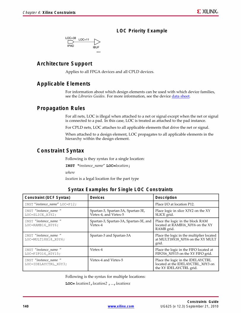
Chapter 4: Xilinx Constraints
LOC Priority Example
Architecture SupportApplies to all FPGA devices and all CPLD devices.
Applicable ElementsFor information about which design elements can be used with which device families,see the Libraries Guides. For more information, see the device data sheet.
Propagation RulesFor all nets, LOC is illegal when attached to a net or signal except when the net or signalis connected to a pad. In this case, LOC is treated as attached to the pad instance.
For CPLD nets, LOC attaches to all applicable elements that drive the net or signal.
When attached to a design element, LOC propagates to all applicable elements in thehierarchy within the design element.
Constraint SyntaxFollowing is they syntax for a single location:
INST “instance_name” LOC=location;
wherelocation is a legal location for the part type
Syntax Examples for Single LOC ConstraintsConstraint (UCF Syntax) Devices DescriptionINST “instance_name” LOC=P12; Place I/O at location P12.
INST “instance_name “LOC=SLICE_X3Y2;
Spartan-3, Spartan-3A, Spartan-3E,Virtex-4, and Virtex-5
Place logic in slice X3Y2 on the XYSLICE grid.
INST “instance_name “LOC=RAMB16_X0Y6;
Spartan-3, Spartan-3A, Spartan-3E, andVirtex-4
Place the logic in the block RAMlocated at RAMB16_X0Y6 on the XYRAMB grid.
INST “instance_name “LOC=MULT18X18_X0Y6;
Spartan-3 and Spartan-3A Place the logic in the multiplier locatedat MULT18X18_X0Y6 on the XY MULTgrid.
INST “instance_name “LOC=FIFO16_X0Y15;
Virtex-4 Place the logic in the FIFO located atFIFO16_X0Y15 on the XY FIFO grid.
INST “instance_name “LOC=IDELAYCTRL_X0Y3;
Virtex-4 and Virtex-5 Place the logic in the IDELAYCTRLlocated at the IDELAYCTRL_X0Y3 onthe XY IDELAYCTRL grid.
Following is the syntax for multiple locations:
LOC= location1,location2 ,...,locationx
Constraints Guide140 www.xilinx.com UG625 (v 12.3) September 21, 2010

Chapter 4: Xilinx Constraints
Separating each such constraint by a comma specifies multiple locations for an element.When you specify multiple locations, PAR can use any of the specified locations.Examples of multiple LOC constraints are provided in the following table.
Multiple LOC Constraint ExamplesConstraint Devices DescriptionINST “instance_name “LOC=SLICE_X2Y10,SLICE_X1Y10;
FPGA Place the logic inSLICE_X2Y10 or inSLICE_X1Y10 on the XYSLICE grid.
Currently, using a single constraint there is no way to constrain multiple elements to asingle location or multiple elements to multiple locations.
Following is the syntax for a range of locations:
INST “ instance_name” LOC=location :location {SOFT };
You can define a range by specifying the two corners of a bounding box. Except forSpartan-3, Spartan-3A, Spartan-3E, Virtex-4, and Virtex-5 devices, specify the upper leftand lower right corners of an area in which logic is to be placed. For FPGA devices,specify the lower left and upper right corners. Use a colon (:) to separate the twoboundaries.
The logic represented by the symbol is placed somewhere inside the bounding box. Thedefault is to interpret the constraint as a “hard” requirement and to place it within thebox. If SOFT is specified, PAR may place the constraint elsewhere if better results can beobtained at a location outside the bounding box. Examples of LOC constraints used tospecify a range are given in the following table.
LOC Range Constraint ExamplesConstraint Devices DescriptionINST “instance_name “LOC=SLICE_X3Y5:SLICE_X5Y20;
FPGA Place logic in any slice withinthe rectangular area bounded bySLICE_X3Y5 (the lower left corner) andSLICE_X5Y20 (the upper right corner)on the XY SLICE grid.
LOC ranges can be supplemented with the keyword SOFT. Unlike AREA_GROUP, LOCranges do not influence the packing of symbols. LOC range is strictly a placementconstraint used by PAR.
Following is the LOC syntax for CPLD devices:
INST “instance_name” LOC=pin_name;
or
INST “ instance_name” LOC=FBff ;
or
INST “instance_name” LOC=FB ff_mm;
where• pin_name is Pnn for numeric pin names or rc for row-column pin names• ff is a function block number• mm is a macrocell number within a function block
The two constraint formats for FBff and FBff_mm are only applicable for outputs andbidirectional pins, not for inputs.
Constraints GuideUG625 (v 12.3) September 21, 2010 www.xilinx.com 141
Chapter 4: Xilinx Constraints
The first constraint format:
INST “instance_name” LOC=pin_name;
is applicable for all types of IO.
Syntax ExamplesFor examples of legal placement constraints for each type of logic element in FPGAdesigns, see Syntax for FPGA Devices for this constraint, and the Relative Location(RLOC) constraint. Logic elements include flip-flops, ROMs and RAMs, block RAMS,FMAPs, BUFTs, CLBs, IOBs, I/Os, edge decoders, and global buffers.
The following examples show how to use this constraint with particular tools ormethods. If a tool or method is not listed, you cannot use this constraint with it.
Schematic Syntax• Attach to an instance• Attribute Name: LOC• Attribute Values: value
For valid values, see Syntax for FPGA Devices and Syntax for CPLD Devices for thisconstraint.
VHDL SyntaxDeclare the VHDL constraint as follows:
attribute loc: string;
Specify the VHDL constraint as follows:
attribute loc of {signal_name| label_name}: {signal |label} is “location”;
Set the LOC constraint on a bus as follows:
attribute loc of bus_name : signal is “ location_1 location_2 location_3...”;
To constrain only a portion of a bus (CPLD devices only), use the following syntax:
attribute loc of bus_name : signal is “* * location_1 * location_2...”;
For more information about location, see Syntax for FPGA Devices and Syntax for CPLDDevices for this constraint.
For more information about basic VHDL syntax, see VHDL Attributes.
Verilog SyntaxPlace the Verilog constraint immediately before the module or instantiation.
Specify the Verilog constraint as follows:
(* LOC = “ location” *)
Set the LOC constraint on a bus as follows:
(* LOC = “location_1 location_2 location_3... ” *)
To constrain only a portion of a bus (CPLD devices only), use the following syntax:
(* LOC = “ * *location_1 location_2...” *)
For more information about location, see Syntax for FPGA Devices and Syntax for CPLDDevices for this constraint.
For more information about basic Verilog syntax, see Verilog Attributes.
Constraints Guide142 www.xilinx.com UG625 (v 12.3) September 21, 2010
Chapter 4: Xilinx Constraints
UCF and NCF SyntaxThe following statement specifies that each instance found under “FLIP_FLOPS” is to beplaced in any CLB in column 8.
INST “/FLIP_FLOPS/*” LOC=SLICE_X*Y8;
The following statement specifies that an instantiation of MUXBUF_D0_OUT be placedin IOB location P110.
INST “MUXBUF_D0_OUT” LOC=P110;
The following statement specifies that the net DATA<1> be connected to the pad fromIOB location P111.
NET “DATA<1>” LOC=P111;
XCF SyntaxBEGIN MODEL “ entity_name”
PIN “signal_name” loc=string ;
INST “instance_name” loc=string ;
END;
PCF SyntaxLOC writes out a LOCATE constraint to the PCF file. For more information, see theLocate (LOCATE) constraint.
PlanAhead™ SyntaxFor more information about using the PlanAhead™ software to create constraints, seeFloorplanning the Design in the PlanAhead User Guide. See PlanAhead in this Guide forinformation about:• Defining placement constraints• Assigning placement constraints• Defining I/O pin configurations• Floorplanning and placement constraints
PACE SyntaxPACE is mainly used to assign location constraints to IOs. It can also be used to assigncertain IO properties such as IO Standards. You can access PACE from the Processeswindow in the Project Navigator.
For more information, see the PACE help, especially the topics within Editing Pinsand Areas in the Procedures section. PACE is supported for CPLD devices only. It isnot supported for FPGA devices.
Digital Clock Manager (DCM) Constraint ExamplesThis section applies to all FPGA devices.
You can lock the DCM in the UCF file. The syntax is as follows:
INST “instance_name" LOC = DCM_X AYB; (for all Spartan devices)
INST “instance_name" LOC = DCM_ADV_X AYB; (for Virtex-4 and Virtex-5 devices)
A is the X coordinate, starting with 0 at the left-hand bottom corner. A increases in valueas you move across the device to the right.
Constraints GuideUG625 (v 12.3) September 21, 2010 www.xilinx.com 143

Chapter 4: Xilinx Constraints
B is the Y coordinate, starting with 0 at the left-hand bottom corner. B increases invalue as you move up the device.
Example
INST “myinstance” LOC = DCM_X0Y0;
Flip-Flop Constraint ExamplesFlip-flop constraints can be assigned from the schematic or through the UCF file.
From the schematic, attach LOC constraints to the target flip-flop. The constraints arethen passed into the EDIF netlist and are read by PAR after the design is mapped.
The following examples show how the LOC constraint is applied to a schematic and toa UCF (User Constraints File). The instance names of two flip-flops, /top-12/fdrd and/top-54/fdsd, are used to show how you would enter the constraints in the UCF.
Slice-Based XY Grid Designations
Spartan-3 devices and higher and Virtex-4 devices and higher are the only architecturesthat use slice-based XY grid designations.
Flip-flops can be constrained to a specific slice, a range of slices, a row or column of slices.
Example One
Place the flip-flop in SLICE_X1Y5. SLICE_X0Y0 is in the lower left corner of the device.
Schematic LOC=SLICE_XlY5
UCF INST “/top-12/fdrd”LOC=SLICE_X1Y5;
Example Two
Place the flip-flop in the rectangular area bounded by the SLICE_X1Y1 in the lower leftcorner and SLICE_X5Y7 in the upper right corner.
Schematic LOC=SLICE_R1C1:SLICE_R5C7
UCF INST “/top-12/fdrd”LOC=SLICE_X1Y1:SLICE_X5Y7;
Example Three
Place the flip-flops anywhere in the row of slices whose Y coordinate is 3. Use thewildcard (*) character in place of either the X or Y value to specify an entire row (Y*)or column (X*) of slices.
Schematic LOC=SLICE_X*Y3
UCF INST “/top-12/fdrd/top-54/fdsd”LOC=SLICE_X*Y3;
Example Four
Place the flip-flop in either SLICE_X2Y4 or SLICE_X7Y9.
Schematic LOC=SLICE_X2Y4,SLICE_X7Y9
UCF INST “/top-54/fdsd” LOC=SLICE_X2Y4,SLICE_X7Y9;
In Example Four, repeating the LOC constraint and separating each such constraint by acomma specifies multiple locations for an element. When you specify multiple locations,PAR can use any of the specified locations.
Example Five
Constraints Guide144 www.xilinx.com UG625 (v 12.3) September 21, 2010

Chapter 4: Xilinx Constraints
Do not place the flip-flop in the column of slices whose X coordinate is 5. Use thewildcard (*) character in place of either the X or Y value to specify an entire row (Y*)or column (X*) of slices.
Schematic PROHIBIT=SLICE_X5Y*
UCF CONFIG PROHIBIT=SLICE_X5Y*;
I/O Constraint ExamplesYou can constrain I/Os to a specific IOB. You can assign I/O constraints from theschematic or through the UCF file.
From the schematic, attach LOC constraints to the target PAD symbol. The constraintsare then passed into the netlist file and read by PAR after mapping.
Alternatively, in the UCF file a pad is identified by a unique instance name. Thefollowing example shows how the LOC constraint is applied to a schematic and toa UCF (User Constraints File). In the examples, the instance names of the I/Os are/top-102/data0_pad and /top-117/q13_pad. The example uses a pin number to lock toone pin.
Schematic LOC=P17
UCF INST “/top-102/data0_pad” LOC=P17;
Place the I/O in the IOB at pin 17. For pin grid arrays, a pin name such as B3 or T1 is used.
IOB Constraint ExamplesYou can assign I/O pads, buffers, and registers to an individual IOB location. IOBlocations are identified by the corresponding package pin designation.
The following examples illustrate the format of IOB constraints. Specify LOC= and thepin location. If the target symbol represents a soft macro containing only I/O elements,for example, INFF8, the LOC constraint is applied to all I/O elements contained in thatmacro. If the indicated I/O elements do not fit into the specified locations, an erroris generated.
The following UCF statement places the I/O element in location P13. For PGA packages,the letter-number designation is used, for example, B3.
INST “ instance_name” LOC=P13;
You can prohibit the mapper from using a specific IOB. You might take this step tokeep user I/O signals away from semi-dedicated configuration pins. Such PROHIBITconstraints can be assigned only through the UCF file.
IOBs are prohibited by specifying a PROHIBIT constraint preceded by the CONFIGkeyword, as shown in the following example.
Schematic None
UCF CONFIG PROHIBIT=p36, p37, p41;
Do not place user I/Os in the IOBs at pins 36, 37, or 41. For pin grid arrays, pin namessuch as D14, C16, or H15 are used.
Mapping Constraint Examples (FMAP)Mapping constraints control the mapping of logic into CLBs. They have two parts.The first part is an FMAP component placed on the schematic. The second is a LOCconstraint that can be placed on the schematic or in the constraints file.
Constraints GuideUG625 (v 12.3) September 21, 2010 www.xilinx.com 145

Chapter 4: Xilinx Constraints
FMAP controls the mapping of logic into function generators. This symbol does notdefine logic on the schematic; instead, it specifies how portions of logic shown elsewhereon the schematic should be mapped into a function generator.
The FMAP symbol defines mapping into a four-input (F) function generator.
For the FMAP symbol as with the CLBMAP primitive, MAP=PUC or PUO is supported,as well as the LOC constraint. (Currently, pin locking is not supported. MAP=PLC orPLO is translated into PUC and PUO, respectively.)
Example One
Place the FMAP symbol in the SLICE at row 7, column 3.
Schematic LOC=SLICE_X7Y3
UCF INST “$1I323”LOC=SLICE_X2Y4,SLICE_X3Y4;
Example Two
Place the FMAP symbol in either the SLICE at row 2, column 4 or the SLICE at row 3,column 4.
Schematic LOC=SLICE_X2Y4, SLICE_X3Y4
UCF INST “top/dec0011”LOC=CLB_R2C4,CLB_R3C4;
Example Three
Place the FMAP symbol in the area bounded by SLICE X5Y5 in the upper left corner andSLICE X10Y8 in the lower right
Schematic LOC=SLICE_X5Y5:SLICE_X10Y8
UCF INST “$3I27”LOC=SLICE_X5Y5:SLICE_X10Y8;
Multiplier Constraint ExamplesThis section applies to FPGA devices.
Multiplier constraints can be assigned from the schematic or through the UCF file. Fromthe schematic, attach the LOC constraints to a multiplier symbol. The constraints arethen passed into the netlist file and after mapping they are read by PAR. For moreinformation on attaching LOC constraints, see the application user guide. Alternatively,in the constraints file a multiplier is identified by a unique instance name.
An FPGA multiplier has a different XY grid specification than slices and block RAMs.
• Spartan-3, Spartan-3A, and Spartan-3E devices are specified usingMULT18X18_X#Y#
• Virtex-4 and Virtex-5 devices are specified using DSP48_X#Y#, where the X and Ycoordinate values correspond to the multiplier grid array.
A multiplier located at MULT18X18_X0Y1 is not located at the same site as a flip-floplocated at SLICE_X0Y1 or a block RAM located at RAMB16_X0Y1.
For example, assume you have a device with two columns of multipliers, each columncontaining two multipliers, where one column is on the right side of the chip and theother is on the left. The multiplier located in the lower left corner is MULT18X18_X0Y0.Because there are only two columns of multipliers, the multiplier located in the upperright corner is MULT18X18_X1Y1.
Constraints Guide146 www.xilinx.com UG625 (v 12.3) September 21, 2010

Chapter 4: Xilinx Constraints
Schematic LOC=MULT18X18_X0Y0
UCF INST “/top-7/rq” LOC=MULT18X18_X0Y0;
ROM Constraint ExamplesMemory constraints can be assigned from the schematic or through the UCF file.
From the schematic, attach the LOC constraints to the memory symbol. The constraintsare then passed into the netlist file and after mapping they are read by PAR. For moreinformation on attaching LOC constraints, see the application user guide.
Alternatively, in the constraints file memory is identified by a unique instance name.One or more memory instances of type ROM can be found in the input file. All memorymacros larger than 16 x 1 or 32 x 1 are broken down into these basic elements in thenetlist file.
In the following examples, the instance name of the ROM primitive is /top-7/rq.
Slice-Based XY Designations
Spartan-3 and higher and Virtex-4 and higher devices use slice-based XY griddesignations. You can constrain a ROM to a specific slice, a range of slices, or a rowor column of slices.
Example One
Place the memory in the SLICE_X1Y1. SLICE_X1Y1 is in the lower left corner of thedevice. You can apply a single-SLICE constraint such as this only to a 16 x 1 or 32 x 1memory.
Schematic LOC=SLICE_X1Y1
UCF INST “/top-7/rq” LOC=SLICE_X1Y1;
Example Two
Place the memory in either SLICE_X2Y4 or SLICE_X7Y9.
Schematic LOC=SLICE_X2Y4, SLICE_X7Y9
UCF INST “/top-7/rq” LOC=SLICE_X2Y4,SLICE_X7Y9;
Example Three
Do not place the memory in column of slices whose X coordinate is 5. You can use thewildcard (*) character in place of either the X or Y coordinate value in the SLICE name tospecify an entire row (Y*) or column (X*) of slices.
Schematic PROHIBIT SLICE_X5Y*
UCF CONFIG PROHIBIT=SLICE_X5Y*;
Block RAM (RAMBs) Constraint ExamplesThis section applies to FPGA devices
Block RAM constraints can be assigned from the schematic or through the UCF file.From the schematic, attach the LOC constraints to the block RAM symbol. Theconstraints are then passed into the netlist file. After mapping they are read by PAR.For more information on attaching LOC constraints, see the application user guide.Alternatively, in the constraints file a memory is identified by a unique instance name.
Spartan-3 and Higher Devices
Constraints GuideUG625 (v 12.3) September 21, 2010 www.xilinx.com 147

Chapter 4: Xilinx Constraints
An FPGA block RAM has a different XY grid specification than a slice or multiplier. It isspecified using RAMB16_Xm Yn where the X and Y coordinate values correspond tothe block RAM grid array. A block RAM located at RAMB16_X0Y1 is not located at thesame site as a flip-flop located at SLICE_X0Y1.
For example, assume you have a device with two columns of block RAM, each columncontaining two blocks, where one column is on the right side of the chip and the other ison the left. The block RAM located in the lower left corner is RAMB16_X0Y0. Becausethere are only two columns of block RAM, the block located in the upper right corneris RAMB16_X1Y1.
Schematic LOC=RAMB16_X0Y0 (for all FPGA devicesexcept Virtex-5 devices)
LOC=RAMB36_X0Y0 (for Virtex-5 devices)
UCF INST “/top-7/rq” LOC=RAMB16_X0Y0;
Slice Constraint ExamplesThis section applies to all FPGA devices These are currently the only architectures thatuse the slice-based XY grid designations.
You can assign soft macros and flip-flops to a single slice location, a list of slice locations,or a rectangular block of slice locations.
Slice locations can be a fixed location or a range of locations. Use the following syntaxto denote fixed locations.
SLICE_XmY n
wherem and n are the X and Y coordinate values, respectively
They must be less than or equal to the number of slices in the target device. Use thefollowing syntax to denote a range of locations from the highest to the lowest.
SLICE_X mYn:SLICE_XmY n
Format of Slice Constraints
The following examples illustrate the format of slice constraints: LOC= and the slicelocation. If the target symbol represents a soft macro, the LOC constraint is applied to allappropriate symbols (flip-flops, maps) contained in that macro. If the indicated logicdoes not fit into the specified blocks, an error is generated.
Slice Constraints Example One
The following UCF statement places logic in the designated slice.
INST “instance_name” LOC=SLICE_X133Y10;
Slice Constraints Example Two
The following UCF statement places logic within the first column of slices. The asterisk(*) is a wildcard character
INST “instance_name” LOC=SLICE_X0Y*;
Slice Constraints Example Three
The following UCF statement places logic in any of the three designated slices. There isno significance to the order of the LOC statements.
INST “ instance_name” LOC=SLICE_X0Y3, SLICE_X67Y120, SLICE_X3Y0;
Slice Constraints Example Four
Constraints Guide148 www.xilinx.com UG625 (v 12.3) September 21, 2010
Chapter 4: Xilinx Constraints
The following UCF statement places logic within the rectangular block defined by thefirst specified slice in the lower left corner and the second specified slice towards theupper right corner.
INST “ instance_name" LOC=SLICE_X3Y22:SLICE_X10Y55;
Slices ProhibitedYou can prohibit PAR from using a specific slice, a range of slices, or a row or columnof slices. Such prohibit constraints can be assigned only through the User ConstraintsFile (UCF). Slices are prohibited by specifying a PROHIBIT constraint at the designlevel, as shown in the following examples.
Slices Prohibited Example One
Do not place any logic in the SLICE_X0Y0. SLICE_X0Y0 is at the lower left corner ofthe device.
Schematic None
UCF CONFIG PROHIBIT=SLICE_X0Y0;
Slices Prohibited Example Two
Do not place any logic in the rectangular area bounded by SLICE_X2Y3 in the lower leftcorner and SLICE_X10Y10 in the upper right.
Schematic None
UCF CONFIGPROHIBIT=SLICE_X2Y3:SLICE_X10Y10;
Slices Prohibited Example Three
Do not place any logic in a slice whose location has 3 as the X coordinate. This designatesa column of prohibited slices. You can use the wildcard (*) character in place of eitherthe X or Y coordinate to specify an entire row (X*) or column (Y*) of slices.
Schematic None
UCF CONFIG PROHIBIT=SLICE_X3Y*;
Slices Prohibited Example Four
Do not place any logic in either SLICE_X2Y4 or SLICE_ X7Y9.
Schematic None
UCF CONFIG PROHIBIT=SLICE_X2Y4,SLICE_X7Y9;
LOCATE (Locate)The LOCATE (Locate) constraint:• Is a basic placement constraint.• Specifies any one of the following:
– a single location– multiple single locations– a location range
Constraints GuideUG625 (v 12.3) September 21, 2010 www.xilinx.com 149
Chapter 4: Xilinx Constraints
Architecture SupportApplies to FPGA devices. Does not apply to CPLD devices.
Applicable Elements• CLB
• IOB
• DCM
• Clock logic• Macros
Propagation Rules• When attached to a macro, LOCATE propagates to all elements of the macro.• When attached to a primitive, LOCATE applies to the entire primitive.
Syntax ExamplesThe following examples show how to use this constraint with particular tools ormethods. If a tool or method is not listed, you cannot use this constraint with it.
Single or Multiple Single Locations PCF SyntaxCOMP “comp_name” LOCATE=[SOFT] “site_item1”... “site_itemn” [LEVEL n];
COMPGRP “group_name” LOCATE=[SOFT] “site_item1”... “site_itemn” [LEVEL n];
MACRO name LOCATE=[SOFT] “site_item1” “site_itemn” [LEVEL n];
Range of Locations PCF SyntaxCOMP “comp_name” LOCATE=[SOFT] SITE “site_name” : SITE “site_name” [LEVEL n];
COMPGRP “group_name” LOCATE=[SOFT] SITE “site_name” : SITE “site_name”[LEVEL n];
MACRO “macro_name” LOCATE=[SOFT] SITE “site_name” : SITE “site_name” [LEVELn];
where• site_name is a component site (that is, a CLB or IOB location)• site_item is one of the following:
– SITE "site_name"– SITEGRP "site_group_name"
• n in LEVEL n is 0, 1, 2, 3, or 4
LOCK_PINS (Lock Pins)The LOCK_PINS (Lock Pins) constraint:• Instructs the implementation tools to not swap the pins of the LUT symbol to which
it is attached.• Is distinct from the Lock Pins process in ISE® Design Suite, which is used to preserve
the existing pinout of a CPLD design.
Constraints Guide150 www.xilinx.com UG625 (v 12.3) September 21, 2010

Chapter 4: Xilinx Constraints
Architecture SupportApplies to FPGA devices. Does not apply to CPLD devices.
Applicable ElementsApplies only to specific instances of LUT symbols.
Propagation RulesApplies only to a single LUT instance.
Syntax ExamplesThe following examples show how to use this constraint with particular tools ormethods. If a tool or method is not listed, you cannot use this constraint with it.
VHDL SyntaxDeclare the VHDL constraint as follows:
attribute lock_pins: string;
Specify the VHDL constraint as follows:
attribute lock_pins of {component_name|label_name} : {component|label} is “all”;
For more information about basic VHDL syntax, see VHDL Attributes.
Verilog SyntaxPlace the Verilog constraint immediately before the module or instantiation.
Specify the Verilog constraint as follows:
(* LOCK_PINS = “all” *)
For more information on basic Verilog syntax, see Verilog Attributes.
UCF and NCF Syntax• Using No Designator
INST “XSYM1” LOCK_PINS;
• Using the ALL Attribute
INST “XSYM1” LOCK_PINS=’ALL’;
• Using a PIN Assignment List
INST I_589 LOCK_PINS=I0:A2;
INST I_894 LOCK_PINS=I3:A1,I2:A4;
INST tvAgy LOCK_PINS=I0:A4,I1:A3,I2:A2,I3:A1;
Constraints GuideUG625 (v 12.3) September 21, 2010 www.xilinx.com 151

Chapter 4: Xilinx Constraints
LUTNM (Lookup Table Name)The LUTNM (Lookup Table Name) constraint:• Allows you to control the grouping of logical symbols into the LUT sites of Virtex®-5
devices.• Is a string value property that is applied to two qualified symbols.• Must be applied uniquely to two symbols within the design. These two symbols are
implemented in a shared LUT site within a SLICE component.• Is functionally similar to BLKNM (Block Name).
Architecture SupportApplies to Virtex-5 devices only.
Applicable ElementsCan be applied to:• Two symbols that are unique within the design• Two 5-input or smaller function generator symbols (LUT, ROM, or RAM) if the total
number of unique input pins required for both symbols does not exceed 5 pins• A 6-input read-only function generator symbol (LUT6, ROM64) in conjunction with
a 5-input read-only symbol (LUT5, ROM32) if:– The total number of unique input pins required for both symbols does not
exceed 6 inputs, and– The lower 32 bits of the 6-input symbol programming matches all 32 bits of the
5-input symbol programming.
Propagation RulesLUTNM can be applied to two symbols that are unique within the design.
Syntax ExamplesThe following examples show how to use this constraint with particular tools ormethods. If a tool or method is not listed, you cannot use this constraint with it.
Schematic Syntax• Attach to a valid element or symbol type• Attribute Name
LUTNM
• Attribute Value<user_defined>
VHDL SyntaxBefore using LUTNM, declare it with the following syntax placed after the architecturedeclaration, but before the begin statement in the top-level VHDL file:
attribute LUTNM: string;
Specify the VHDL constraint as follows:
attribute LUTNM of {LUT5_instance_name}: label is "value";
Constraints Guide152 www.xilinx.com UG625 (v 12.3) September 21, 2010

Chapter 4: Xilinx Constraints
where
value
is any chosen name under which you want to group the two elements.
Example
architecture MY_DESIGN of top isattribute LUTNM: string;
attribute LUTNM of LUT5_inst1: label is "logic_group1";attribute LUTNM of LUT5_inst2: label is "logic_group1";
begin-- LUT5: 5-input Look-Up Table
-- Virtex-5-- Xilinx HDL Libraries Guide version 8.2i
LUT5_inst1 : LUT5generic map (
INIT => X"a49b44c1")port map (
O => aout, -- LUT output (1-bit)I0 => d(0), -- LUT input (1-bit)I1 => d(1), -- LUT input (1-bit)I2 => d(2), -- LUT input (1-bit)I3 => d(3), -- LUT input (1-bit)I4 => d(4) -- LUT input (1-bit)
);-- End of LUT5_inst1 instantiation-- LUT5: 5-input Look-Up Table
-- Virtex-5-- Xilinx HDL Libraries Guide version 8.2i
LUT5_inst2 : LUT5generic map (
INIT => X"649d610a")port map (
O => bout, -- LUT output (1-bit)I0 => d(0), -- LUT input (1-bit)I1 => d(1), -- LUT input (1-bit)I2 => d(2), -- LUT input (1-bit)I3 => d(3), -- LUT input (1-bit)I4 => d(4) -- LUT input (1-bit)
);-- End of LUT5_inst2 instantiationEND MY_DESIGN;
For more information about basic VHDL syntax, see VHDL Attributes.
Verilog SyntaxPlace the following attribute specification before the port declaration in the top-levelVerilog code:
(* LUTNM = "value" *)
where
value is any chosen name under which you want to group the two elements.
Constraints GuideUG625 (v 12.3) September 21, 2010 www.xilinx.com 153

Chapter 4: Xilinx Constraints
Example
// LUT5: 5-input Look-Up Table// Virtex-5// Xilinx HDL Libraries Guide version 8.2i(* LUTNM="logic_group1" *) LUT5 #(
.INIT(32’ha49b44c1)) LUT5_inst1 (
.O(aout), // LUT output (1-bit)
.I0(d[0]), // LUT input (1-bit)
.I1(d[1]), // LUT input (1-bit)
.I2(d[2]), // LUT input (1-bit)
.I3(d[3]), // LUT input (1-bit)
.I4(d[4]) // LUT input (1-bit));// End of LUT5_inst1 instantiation// LUT5: 5-input Look-Up Table// Virtex-5// Xilinx HDL Libraries Guide version 8.2i(* LUTNM="logic_group1" *) LUT5 #(
.INIT(32’h649d610a)) LUT5_inst2 (
.O(bout), // LUT output (1-bit)
.I0(d[0]), // LUT input (1-bit)
.I1(d[1]), // LUT input (1-bit)
.I2(d[2]), // LUT input (1-bit)
.I3(d[3]), // LUT input (1-bit)
.I4(d[4]) // LUT input (1-bit));// End of LUT5_inst2 instantiation
For more information about basic Verilog syntax, see Verilog Attributes.
UCF and NCF SyntaxPlaced on the output, or bi-directional port:
INST "LUT5_instance_name" LUTNM="value";
Where value is any chosen name under which you want to group the two elements.
Example
INST "LUT5_inst1" LUTNM="logic_group1";
INST "LUT5_inst2" LUTNM="logic_group1";
MAP (Map)MAP (Map) is an advanced mapping constraint. Place MAP on an FMAP to specifywhether pin swapping and the merging of other functions with the logic in the map areallowed. If merging with other functions is allowed, other logic can also be placedwithin the CLB, if space allows.
Architecture SupportApplies to FPGA devices. Does not apply to CPLD devices.
Applicable ElementsFMAP
Constraints Guide154 www.xilinx.com UG625 (v 12.3) September 21, 2010

Chapter 4: Xilinx Constraints
Propagation RulesApplies to the design element to which it is attached
SyntaxThe following examples show how to use this constraint with particular tools ormethods. If a tool or method is not listed, you cannot use this constraint with it.
UCF and NCF SyntaxINST “ instance_name” MAP=[PUC | PUO | PLC | PLO] ;
where• PUC
The CLB pins are unlocked (U) and the CLB is closed (C). The software can swapsignals among the pins on the CLB, but cannot add or remove logic from the CLB.
• PUO (default)The CLB pins are unlocked (U) and the CLB is open (O). The software can swapsignals among the pins on the CLB, and can add or remove logic from the CLB.
• PLCThe CLB pins are locked (L) and the CLB is closed (C). The software cannot swapsignals among the pins on the CLB, and cannot add or remove logic from the CLB.
• PLOThe CLB pins are locked (L) and the CLB is open (O). The software cannot swapsignals among the pins on the CLB, but can add or remove logic from the CLB.
Currently, only PUC and PUO are observed. PLC and PLO are translated into PUCand PUO, respectively.
The following statement allows pin swapping, and ensures that no logic other than thatdefined by the original map is mapped into the function generators.
INST “$1I3245/map_of_the_world” map=puc;
MAX_FANOUT (Max Fanout)MAX_FANOUT (Max Fanout) limits the fanout of nets or signals. Depending on thevalue of the constraint, both XST and MAP limit the fanout of a net when this constraintis applied. The value can either be an integer (XST only) or REDUCE (MAP only).
MAX_FANOUT for XST
Default integer values for XST are shown in the following table. Max Fanout is both aglobal and a local constraint in XST.
Max Fanout Default Values DevicesDevices Default ValueSpartan®-3, Spartan-3E, Spartan-3A,Spartan-3A D
500
Virtex®-4 500
Virtex-5 100000 (One Hundred Thousand)
Constraints GuideUG625 (v 12.3) September 21, 2010 www.xilinx.com 155

Chapter 4: Xilinx Constraints
Large fanouts can cause routability problems. XST tries to limit fanout by duplicatinggates or by inserting buffers. This limit is not a technology limit but a guide to XST. Itmay happen that this limit is not exactly respected, especially when this limit is small(less than 30).
In most cases, fanout control is performed by duplicating the gate driving the net with alarge fanout. If the duplication cannot be performed, buffers are inserted. These buffersare protected against logic trimming at the implementation level by defining a Keep(KEEP) attribute in the NGC file. If the register replication option is set to no, onlybuffers are used to control fanout of flip-flops and latches.
Max Fanout is global for the design, but you can control maximum fanout independentlyfor each entity or module or for given individual signals by using constraints.
If the actual net fanout is less than the Max Fanout value, XST behavior depends on howMax Fanout is specified.• If the value of Max Fanout is set in ISE® Design Suite in the command line, or is
attached to a specific hierarchical block, XST interprets its value as a guidance.• If Max Fanout is attached to a specific net, XST does not perform logic replication.
Putting Max Fanout on the net may prevent XST from having better timingoptimization.
For example, suppose that the critical path goes through the net, which actual fanout is80 and set Max Fanout value to 100. If Max Fanout is specified in ISE Design Suite, XSTmay replicate it, trying to improve timing. If Max Fanout is attached to the net itself,XST does not perform logic replication.
MAX_FANOUT for MAP
MAX_FANOUT can also drive MAP to limit fanout by duplicating registers and/orgates. The MAP register duplication option (-register_duplication) must be enabledand MAX_FANOUT constraints must be applied locally to nets for this to occur. Whenused during MAP, only the value of REDUCE is accepted. WhenMAX_FANOUT =“REDUCE”, MAP limits fanout if it determines that it can provide an improvementin performance with out causing problems in fitting the design. Review the physicalsynthesis report (*PSR) generated by MAP to review whether or notMAX_FANOUT =“REDUCE” caused fanout reduction to actually occur.
Architecture SupportApplies to all FPGA devices. Does not apply to CPLD devices.
Applicable ElementsWhen the value is an integer, Max Fanout applies globally, or to a VHDL entity, a Verilogmodule, or signal.
When the value is REDUCE, Max Fanout applies only to a signal.
Propagation RulesApplies to the entity, module, or signal to which it is attached.
Syntax ExamplesThe following examples show how to use this constraint with particular tools ormethods. If a tool or method is not listed, you cannot use this constraint with it.
VHDL SyntaxDeclare the VHDL constraint as follows:
Constraints Guide156 www.xilinx.com UG625 (v 12.3) September 21, 2010

Chapter 4: Xilinx Constraints
attribute max_fanout: string;
Specify the VHDL constraint as follows:
attribute max_fanout of {signal_name|entity_name}: {signal|entity} is "integer";
For more information about basic VHDL syntax, see VHDL Attributes.
Verilog SyntaxPlace the Verilog constraint immediately before the module or instantiation.
Specify the Verilog constraint as follows:
(* max_fanout = "integer" *)
XCF Syntax Example OneMODEL "entity_name" max_fanout=integer;
XCF Syntax Example TwoBEGIN MODEL "entity_name"
NET "signal_name" max_fanout=integer;
END;
XST Command Line SyntaxDefine globally with the -max_fanout command line option of the run command:
-max_fanout integer
ISE Design Suite SyntaxDefine globally in ISE Design Suite in Process > Properties > Xilinx-Specific Options >Max Fanout.
UCF SyntaxWhen used with the MAP Register Duplication option, specify MAX_FANOUT in theUser Constraints File (UCF) as follows:
NET "signal_name" max_fanout=REDUCE;
MAXDELAY (Maximum Delay)MAXDELAY (Maximum Delay) defines the maximum allowable delay on a net.
Architecture SupportApplies to FPGA devices. Does not apply to CPLD devices.
Applicable ElementsApplies to the net to which it is attached.
Propagation RulesApplies to the net to which it is attached
Constraints GuideUG625 (v 12.3) September 21, 2010 www.xilinx.com 157

Chapter 4: Xilinx Constraints
SyntaxThe following examples show how to use this constraint with particular tools ormethods. If a tool or method is not listed, you cannot use this constraint with it.
Schematic Syntax• Attach to a net
• Attribute Name: MAXDELAY
• Attribute Values: value units
where
value is the numerical time delay
units are:
– micro
– ms
– ns
– ps
VHDL SyntaxDeclare the VHDL constraint as follows:
attribute maxdelay: string;
Specify the VHDL constraint as follows:
attribute maxdelay of signal_name: signal is “value [units]”;
where
• value is any positive integer
• units are:
– ps
– ns (default)
– micro
– ms
– GHz
– MHz
– kHz
For more information on basic VHDL syntax, see VHDL Attributes.
Verilog SyntaxPlace the Verilog constraint immediately before the module or instantiation.
Specify the Verilog constraint as follows:
(*MAXDELAY = “value [units]” *)
Constraints Guide158 www.xilinx.com UG625 (v 12.3) September 21, 2010
Chapter 4: Xilinx Constraints
where• value is any positive integer• units are:
– ps
– ns (default)– micro
– ms
– GHz
– MHz
– kHz
For more information on basic Verilog syntax, see Verilog Attributes.
UCF and NCF SyntaxNET “net_name” MAXDELAY=value units;
where• value is the numerical time delay.• units are:
– micro
– ns
– ms
– ms
The following statement assigns a maximum delay of 10 nanoseconds to the net $SIG_4.
NET “$1I3245/$SIG_4” MAXDELAY=10 ns;
PCF Syntaxitem MAXDELAY = maxvalue [PRIORITY integer];
where• item can be:
– ALLNETS
– NET name– TIMEGRP name– ALLPATHS
– PATH name– path specification
• maxvalue can be a:– numerical time value with units of micro, ms, ps, or ns– numerical frequency value with units of GHz, MHz, or KHz– TSidentifier
Constraints Editor SyntaxTo open Constraints Editor, select ISE® Design Suite > Processes > User Constraints >Exceptions > Timing Constraints > Nets.
Constraints GuideUG625 (v 12.3) September 21, 2010 www.xilinx.com 159
Chapter 4: Xilinx Constraints
FPGA Editor SyntaxTo set MAXDELAY to all paths or nets, select File > Main Properties > Global PhysicalConstraints.
To set MAXDELAY to a selected path or net, with a routed net selected, select Edit >Properties of Selected Items > Physical Constraints.
MAXPT (Maximum Product Terms)The MAXPT (Maximum Product Terms) constraint:• Is an advanced constraint.• Applies to CPLD devices only.• Specifies the maximum number of product terms the fitter is permitted to use when
collapsing logic into the node to which MAXPT is applied.• Overrides the Collapsing P-term Limit setting in ISE® Design Suite for the attached
node.
Architecture SupportApplies to CPLD devices only. Does not apply to FPGA devices.
Applicable ElementsApplies to signals.
Propagation RulesApplies to the signal to which it is attached.
Syntax ExamplesThe following examples show how to use this constraint with particular tools ormethods. If a tool or method is not listed, you cannot use this constraint with it.
VHDL SyntaxDeclare the VHDL constraint as follows:
attribute maxpt: integer;
Specify the VHDL constraint as follows:
attribute maxpt of signal_name : signal is “integer”;
integer is any positive integer
For more information about basic VHDL syntax, see VHDL Attributes.
Verilog SyntaxPlace the Verilog constraint immediately before the module or instantiation.
Specify the Verilog constraint as follows:
(* MAXPT = “integer” *)
integer is any positive integer
For more information about basic Verilog syntax, see Verilog Attributes.
Constraints Guide160 www.xilinx.com UG625 (v 12.3) September 21, 2010
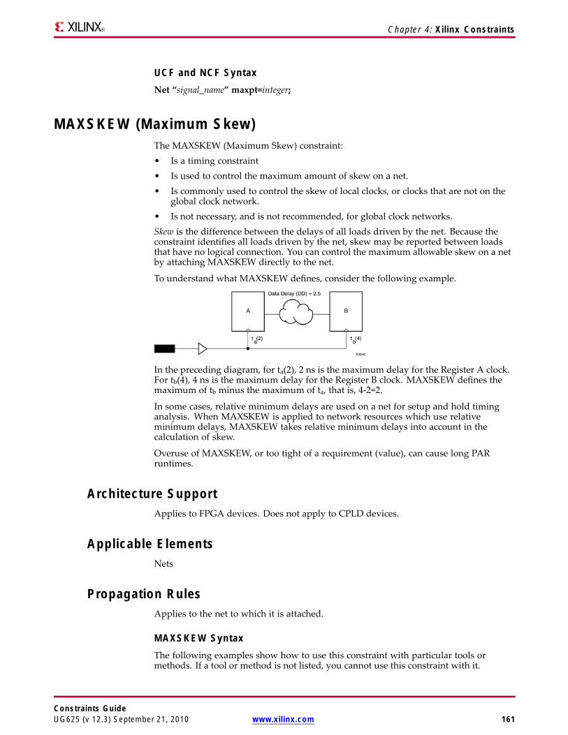
Chapter 4: Xilinx Constraints
UCF and NCF SyntaxNet “signal_name” maxpt=integer;
MAXSKEW (Maximum Skew)The MAXSKEW (Maximum Skew) constraint:• Is a timing constraint• Is used to control the maximum amount of skew on a net.• Is commonly used to control the skew of local clocks, or clocks that are not on the
global clock network.• Is not necessary, and is not recommended, for global clock networks.Skew is the difference between the delays of all loads driven by the net. Because theconstraint identifies all loads driven by the net, skew may be reported between loadsthat have no logical connection. You can control the maximum allowable skew on a netby attaching MAXSKEW directly to the net.
To understand what MAXSKEW defines, consider the following example.
In the preceding diagram, for ta(2), 2 ns is the maximum delay for the Register A clock.For tb(4), 4 ns is the maximum delay for the Register B clock. MAXSKEW defines themaximum of tb minus the maximum of ta, that is, 4-2=2.
In some cases, relative minimum delays are used on a net for setup and hold timinganalysis. When MAXSKEW is applied to network resources which use relativeminimum delays, MAXSKEW takes relative minimum delays into account in thecalculation of skew.
Overuse of MAXSKEW, or too tight of a requirement (value), can cause long PARruntimes.
Architecture SupportApplies to FPGA devices. Does not apply to CPLD devices.
Applicable ElementsNets
Propagation RulesApplies to the net to which it is attached.
MAXSKEW SyntaxThe following examples show how to use this constraint with particular tools ormethods. If a tool or method is not listed, you cannot use this constraint with it.
Constraints GuideUG625 (v 12.3) September 21, 2010 www.xilinx.com 161
Chapter 4: Xilinx Constraints
Schematic Syntax• Attach to a net• Attribute Name
MAXSKEW
• Attribute Valuesallowable_skew
units
where– allowable_skew is the timing requirement– units are ms, micro, ns (default), or ps
VHDL SyntaxDeclare the VHDL constraint as follows:
attribute maxskew: string;
Specify the VHDL constraint as follows:
attribute maxskew of signal_name : signal is “allowable_skew [units]”;
where• allowable_skew is the timing requirement• units are ms, micro, ns (default), or ps
For more information about basic VHDL syntax, see VHDL Attributes.
Verilog SyntaxPlace the Verilog constraint immediately before the module or instantiation.
Specify the Verilog constraint as follows:
(* MAXSKEW = “allowable_skew [units] ” *)
where• allowable_skew is the timing requirement• units are ms, micro, ns (default), or ps
For more information about basic Verilog syntax, see Verilog Attributes.
UCF and NCF SyntaxNET “ net_name” MAXSKEW=allowable_skew [units];
where• allowable_skew is the timing requirement• units are ms, micro, ns (default), or ps
The following statement specifies a maximum skew of 3 ns on net $SIG_6.
NET “$1I3245/$SIG_6” MAXSKEW=3 ns;
Constraints Editor SyntaxFor information on setting constraints in Constraints Editor, including syntax, see theConstraints Editor Help.
Constraints Guide162 www.xilinx.com UG625 (v 12.3) September 21, 2010
Chapter 4: Xilinx Constraints
FPGA Editor SyntaxTo set constraints in FPGA Editor, select Edit > Properties of Selected Items. With arouted net selected, you can set MAXSKEW from the Physical Constraints tab.
MCB Performance (MCB_PERFORMANCE)Note This constraint applies to Spartan®-6 devices only.
Spartan-6 devices have a Memory Controller Block (MCB) which can support twodifferent performance targets depending on voltage settings and conditions on theVCCINT power supply. The performance targets are listed in the device data sheet. Tospecify the desired MCB performance level in the ISE® Design Suite tools, use the MCBPerformance (MCB_PERFORMANCE) configuration constraint in the User ConstraintsFile (UCF) supplied to the tools upon implementation.
MCB_PERFORMANCE is supported in the User Constraints File (UCF) only.
The syntax is as follows:
CONFIG MCB_PERFORMANCE=[STANDARD|EXTENDED];
MCB_PERFORMANCE can be specified as follows:• None
If MCB_PERFORMANCE is not specified, the default is STANDARD.• STANDARD
To target the MCB to normal performance and the full voltage range on VCCINT asshown in the device data sheet, specify STANDARD in the UCF.CONFIG MCB_PERFORMANCE= STANDARD;
• EXTENDEDTo target the MCB to a faster performance, specify EXTENDED in the UCF.CONFIG MCB_PERFORMANCE=EXTENDED;There are explicit voltage requirements when using EXTENDED. For moreinformation, see the device data sheet.
Note VCCINT voltage settings in the UCF and timing tools, and as reported by theISE Design Suite tools, are independent of this setting. They may report a differentvoltage for analysis than required by the MCB_PERFORMANCE setting. Voltagerequirements of this rail must be set properly based on both this attribute and theVoltage settings for timing analysis.
MIODELAY_GROUP (MIODELAY Group)The MIODELAY_GROUP (MIODELAY Group) constraint:• Is a design implementation constraint.• Combines two or more IODELAY_GROUP constraints into a single Master
IODELAY_GROUP to enable automatic replication and placement of IDELAYCTRLconstraints in a design.
Architecture SupportMIODELAY_GROUP applies to Virtex®-4 and Virtex-5 devices. For Virtex-4 devices,MIODELAY_GROUP is supported only when using the Timing Driven Pack andPlacement Option in MAP.
Constraints GuideUG625 (v 12.3) September 21, 2010 www.xilinx.com 163
http://www.xilinx.com/cgi-bin/SW_Docs_Redirect/sw_docs_redirect?locale=en&topic=list+all+data+sheets
Chapter 4: Xilinx Constraints
Applicable ElementsMIODELAY_GROUP is applied to two or more defined IODELAY_GROUPs.
Propagation RulesMIODELAY_GROUP is applied to an existing IODELAY_GROUP. TheMIODELAY_GROUP is propagated to all of the design elements that belonged to theoriginal IODELAY_GROUP. It is illegal to attach MIODELAY_GROUP to a net, signal,or pin.
Syntax ExamplesThe following examples show how to use this constraint with particular tools ormethods. If a tool or method is not listed, you cannot use this constraint with it.
UCF SyntaxMIODELAY_GROUP "master_group_name" = iodelay_group1 iodelay_group2 ... ;
where• master_group_name
– represents the master group being defined– contains all of the elements in iodelay_group1 and iodelay_group2
• iodelay_group1 and iodelay_group2 are predefined IODELAY groups
NODELAY (No Delay)The NODELAY (No Delay) constraint:• Is an advanced mapping constraint.
The default configuration of IOB flip-flops in designs includes an input delay thatresults in no external hold time on the input data path. This delay can be removedby placing NODELAY on input flip-flops or latches, resulting in a smaller setuptime but a positive hold time. The input delay element is active in the defaultconfiguration for Spartan®-3, Spartan-3A, and Spartan-3E devices.
• Can be attached to I/O symbols and the following special function access symbols:– TDI
– TMS
– TCK
Architecture SupportSpartan-3, Spartan-3A, and Spartan-3E devices are supported.
IOBDELAY=NONE, which is applicable to all FPGA devices, is the preferred methodof applying this constraint. For more information see IOBDELAY (Input Output BlockDelay).
Applicable ElementsInput register
You can also attach NODELAY to a net connected to a pad component in a UserConstraints File (UCF). NGDBuild transfers the constraint from the net to the padinstance in the NGD file so that it can be processed by the mapper. Use the followingUCF syntax:
Constraints Guide164 www.xilinx.com UG625 (v 12.3) September 21, 2010
Chapter 4: Xilinx Constraints
NET “ net_name” NODELAY;
Propagation RulesNODELAY is illegal when attached to a net or signal except when the net or signal isconnected to a pad. In this case, NODELAY is treated as attached to the pad instance.
When attached to a design element, NODELAY is propagated to all applicable elementsin the hierarchy within the design element.
Syntax ExamplesThe following examples show how to use this constraint with particular tools ormethods. If a tool or method is not listed, you cannot use this constraint with it.
Schematic Syntax• Attach to a valid instance• Attribute Name
NODELAY
• Attribute ValuesTRUE
FALSE
VHDL SyntaxDeclare the VHDL constraint as follows:
attribute nodelay: string;
Specify the VHDL constraint as follows:
attribute nodelay of {component_name|signal_name|label_name} :{component|signal|label} is “{TRUE|FALSE}”;
For more information about basic VHDL syntax, see VHDL Attributes.
Verilog SyntaxPlace the Verilog constraint immediately before the module or instantiation.
Specify the Verilog constraint as follows:
(* NODELAY = “{TRUE|FALSE}” *)
For more information about basic Verilog syntax, see Verilog Attributes.
UCF and NCF SyntaxThe following statement specifies that IOB register inreg67 not have an input delay.
INST “$1I87/inreg67” NODELAY;
The following statement specifies that there be no input delay to the pad that is attachedto net1.
NET “net1” NODELAY;
XCF SyntaxBEGIN MODEL “entity_name ”
NET "signal_name" nodelay=true;
INST "instance_name" nodelay=true;
Constraints GuideUG625 (v 12.3) September 21, 2010 www.xilinx.com 165

Chapter 4: Xilinx Constraints
END;
NOREDUCE (No Reduce)The NOREDUCE (No Reduce) constraint:• Is a fitter and synthesis constraint.• Prevents minimization of redundant logic terms that are typically included in a
design to avoid logic hazards or race conditions.• Identifies the output node of a combinatorial feedback loop to ensure correct
mapping.When constructing combinatorial feedback latches in a design, always applyNOREDUCE to the latch’s output net and include redundant logic terms when necessaryto avoid race conditions.
Architecture SupportApplies to CPLD devices only. Does not apply to FPGA devices.
Applicable ElementsApplies to the net to which it is attached.
Propagation RulesThis constraint is a net constraint. Any attachment to a design element is illegal.
Syntax ExamplesThe following examples show how to use this constraint with particular tools ormethods. If a tool or method is not listed, you cannot use this constraint with it.
Schematic Syntax• Attach to a net• Attribute Name
NOREDUCE
• Attribute Values– TRUE
– FALSE
VHDL SyntaxDeclare the VHDL constraint as follows:
attribute NOREDUCE: string;
Specify the VHDL constraint as follows:
attribute NOREDUCE of signal_name: signal is “{TRUE|FALSE}”;
For more information about basic VHDL syntax, see VHDL Attributes.
Verilog SyntaxPlace the Verilog constraint immediately before the module or instantiation.
Specify the Verilog constraint as follows:
Constraints Guide166 www.xilinx.com UG625 (v 12.3) September 21, 2010

Chapter 4: Xilinx Constraints
(* NOREDUCE = “{TRUE|FALSE}” *)
For more information about basic Verilog syntax, see Verilog Attributes.
UCF and NCF SyntaxThe following statement specifies that there be no Boolean logic reduction or logiccollapse from the net named $SIG_12 forward.
NET “$SIG_12” NOREDUCE;
XCF SyntaxBEGIN MODEL “entity_name”
NET “signal_name” noreduce={true | false};
END;
OFFSET IN (Offset In)The OFFSET IN (Offset In) constraint:• Specifies the timing requirements of an input interface to the FPGA device.• Specifies the clock and data timing relationship at the external pads of the FPGA
device.An OFFSET IN constraint specification checks the setup and hold timing requirementsof all synchronous elements associated with the constraint.
The OFFSET IN constraint is specified using a clock net name. The clock net associatedwith the OFFSET IN constraint is the external clock pad. Because the constraint specifiesthe clock and data relationship at the external pads of the FPGA, the OFFSET INconstraint cannot be specified using an internal clock net. However, the OFFSET INconstraint automatically accounts for any phase or delay adjustments on the clock pathdue to components such as the DCM, PLL, MMCM, or IDELAY when analyzing thesetup and hold timing requirements at the capturing synchronous element. In addition,the constraint propagates through the clock network and automatically applies to allclocks derived from the original external clock.
The OFFSET IN constraint is global in scope by default. In the global OFFSET INconstraint, all synchronous elements that are clocked by the specified clock net, andcapture external data, are covered by the constraint. The scope of the synchronouselements covered by the constraint can be restricted by specifying time groups on asubset of input data pads, a subset of the capturing synchronous elements, or both.
Architecture SupportApplies to all FPGA devices and all CPLD devices.
Applicable Elements• Global• Net-Specific• Pad Time Group
Syntax ExamplesThe following examples show how to use this constraint with particular tools ormethods. If a tool or method is not listed, you cannot use this constraint with it.
Constraints GuideUG625 (v 12.3) September 21, 2010 www.xilinx.com 167

Chapter 4: Xilinx Constraints
Although User Constraints File (UCF) examples are given below, Xilinx® recommendsspecifying the OFFSET IN constraint using Constraints Editor.
Global MethodThe global method is the default OFFSET IN constraint. The global OFFSET INconstraint applies to all synchronous elements that capture incoming data and aretriggered by the specified clock signal.
Global Method UCF Syntax ExampleOFFSET = IN “offset_time” [units] [VALID <datavalid_time> [UNITS]] {BEFORE|AFTER}“clk_name” [{RISING|FALLING}];
Global Method PCF Syntax ExampleOFFSET = IN “offset_time” [units] [VALID <datavalid_time> [UNITS]] {BEFORE|AFTER}COMP “clk_iob_name” [{RISING|FALLING}];
where
• “offset_time” [units] is the difference in time between the capturing clock edge and thestart of the data to be captured. The time can be specified with or without explicitlydeclaring the units. If no units are specified, the default value is nanoseconds. Thevalid values for this parameter are: ps, ns, micro, and ms.
• [VALID <datavalid_time> [UNITS]] is the valid duration of the data to be captured.This field is required for a hold time verification of the input interface. This valuecan be specified with or without explicitly declaring the units. If no units arespecified, the default value is nanoseconds. The valid values for this field are: ps,ns, micro, and ms.
• BEFORE|AFTER defines the timing relationship of the start of data to the clockedge. The best method of defining the clock and data relationship is to use theBEFORE option. BEFORE describes the time the data begins to be valid relative tothe capturing clock edge. Positive values of BEFORE indicate the data begins priorto the capturing clock edge. Negative values of BEFORE indicate the data beginsfollowing the capturing clock edge.
• “clk_name” defines the fully hierarchical name of the input clock pad net.
• RISING|FALLING are the optional keywords used to define the capturing clockedge in which the clock and data relationship is specified against. In addition, theseuse of these keywords automatically partition rising and falling edge registers indual data rate (DDR) interfaces into separate groups for analysis.
Input Group MethodWhen a group of inputs captured by the same clock have a shared timing requirement,the inputs can be grouped together to create a single timing constraint. The inputs canbe grouped together by input signal names using pad groups, or by the synchronouselements using register groups. By grouping separate signals together into a single timegroup, the memory and runtime of the implementation tools is reduced. In addition, thetiming report will contain bus-based skew and clock centering information.
Input Group Method UCF Syntax Example[TIMEGRP “pad_groupname”] OFFSET = IN “offset_time” [units] [VALID<datavalid_time> [UNITS]] {BEFORE|AFTER} “clk_name” [TIMEGRP “reg_groupname”][{RISING|FALLING}];
Constraints Guide168 www.xilinx.com UG625 (v 12.3) September 21, 2010

Chapter 4: Xilinx Constraints
Input Group Method PCF Syntax Example[TIMEGRP “inputpad_grpname”] OFFSET = IN “offset_time” [units] [VALID<datavalid_time> [UNITS]] {BEFORE|AFTER} COMP “clk_iob_name” [TIMEGRP“reg_groupname”] [{RISING|FALLING}];
where• [TIMEGRP “pad_groupname”] is the optional input pad time group. This time group
can be used to limit the scope of the OFFSET IN constraint to only the synchronouselements fed by the input pad nets contained in the timegroup.
• [TIMEGRP “reg_groupname”] is the optional synchronous element time group. Thistime group can be used to limit the scope of the OFFSET IN constraint to only thesynchronous elements which capture input data with the specified clock and arecontained in the time group.
Net Specific MethodOFFSET IN can also be used to specify an input constraint for a specific data net in aschematic, a specific input pad net in the UCF, or a specific input component in thePCF file.
Schematic Syntax When Attached to a Net
OFFSET = IN “offset_time” [units] [VALID <datavalid_time> [UNITS]] {BEFORE|AFTER}“clk_name” [TIMEGRP “reg_groupname”] [{RISING|FALLING}];
Net Specific Method UCF Syntax ExampleNET “pad_net_name”OFFSET = IN “offset_time” [units] [VALID <datavalid_time> [UNITS]]{BEFORE|AFTER} “clk_name” [TIMEGRP “reg_groupname”] [{RISING|FALLING}];
Net Specific Method PCF Syntax ExampleCOMP “pad_net_name” OFFSET = IN “offset_time” [units] [VALID <datavalid_time>[UNITS]] {BEFORE|AFTER} COMP “clk_iob_name” [TIMEGRP “reg_groupname”][{RISING|FALLING}];
where• pad_net_name” is the name of the input data net attached to the pad.
For the definition of the other variables and keywords, see Global Method above.• The PCF specification uses IO Blocks (COMPs) instead of NETs.
If the IOB COMP name is omitted in the PCF, or the NET name is omitted in theUCF, the OFFSET IN specification is assumed to be global.
UCF Source Synchronous DDR Edge Aligned ExampleThe Source Synchronous Dual Data Rate (DDR) Edge aligned case consists of aninterface where the clock is sent from the transmitting device edge aligned with the datato the FPGA. In a dual data rate interface, data is captured with both the rising andfalling clock edges. In the DDR case, separate OFFSET IN constraints must be definedfor the rising and falling clock edge registers capturing the data. The use of the RISINGand FALLING keywords with the OFFSET IN constraint simplifies this task.
Example WaveformIn this example a dual data rate interface is shown with a clock period of 5 ns and 50/50duty cycle. The rising and falling data is valid for 2 ns and is centered in the high andlow portion of the clock waveform. This results in a 250 ps margin before and afterdata valid window.
Constraints GuideUG625 (v 12.3) September 21, 2010 www.xilinx.com 169
Chapter 4: Xilinx Constraints
Rising Edge ConstraintsThe rising edge OFFSET IN constraint defines the time that the data becomes valid priorto rising clock edge used to capture the data. In this example, the data becomes valid 250ps after the rising clock edge. This results in anOFFSET IN BEFORE value of -250 ps withthe value negative because it begins after the clock edge. Once the data begins, it remainsvalid for 2 ns. This results in a VALID value of 2 ns. The RISING keyword is used withthis constraint to indicate that the constraint applies to only the rising edge synchronouselements, and that the OFFSET IN BEFORE value is specified to the rising clock edge.
Falling Edge ConstraintsThe falling edge OFFSET IN constraint defines the time that the data becomes validprior to falling clock edge used to capture the data. In this example, the data becomesvalid 250 ps after the falling clock edge. This results in an OFFSET IN BEFORE valueof -250 ps with the value negative because it begins after the clock edge. Once the databegins, it remains valid for 2 ns. This results in a VALID value of 2 ns. The FALLINGkeyword is used with this constraint to indicate that the constraint applies to only thefalling edge synchronous elements, and that the OFFSET IN BEFORE value is specifiedto the falling clock edge.
For more information about the RISING and FALLING keywords, see the TimingConstraints User Guide.
UCF SyntaxThe complete UCF syntax of the clock PERIOD and OFFSET IN constraint for theexample is shown below.
NET “clock” TNM<_NET = CLK;TIMESPEC TS_CLK = PERIOD CLK 5.0 ns HIGH 50%;
OFFSET = IN -250 ps VALID 2 ns BEFORE clock RISING;OFFSET = IN -250 ps VALID 2 ns BEFORE clock FALLING
UCF Source Synchronous DDR Center Aligned ExampleThe Source Synchronous Dual Data Rate (DDR) Center aligned case consists of aninterface where the clock is sent from the transmitting device aligned with the center ofthe data. In a dual data rate interface, data is captured with both the rising and fallingclock edges. In the DDR case, separate OFFSET IN constraints must be defined forthe rising and falling clock edge registers capturing the data. Using the RISING andFALLING keywords with the OFFSET IN constraint simplifies this task.
Example WaveformIn this example a dual data rate interface is shown with a clock period of 5 ns and 50/50duty cycle. The rising and falling data is valid for 2 ns and is centered over the high andlow clock edges. This results in a 250 ps margin before and after data valid window.
Rising Edge ConstraintsThe rising edge OFFSET IN constraint defines the time that the data becomes valid priorto rising clock edge used to capture the data. In this example, the data becomes valid 1 nsbefore the rising clock edge. This results in anOFFSET IN BEFORE value of 1 ns with thevalue positive because it begins before the clock edge. Once the data begins, it remainsvalid for 2 ns. This results in a VALID value of 2 ns. The RISING keyword is used withthis constraint to indicate that the constraint applies to only the rising edge synchronouselements, and that the OFFSET IN BEFORE value is specified to the rising clock edge.
Constraints Guide170 www.xilinx.com UG625 (v 12.3) September 21, 2010
Chapter 4: Xilinx Constraints
Falling Edge ConstraintsThe falling edge OFFSET IN constraint defines the time that the data becomes validprior to falling clock edge used to capture the data. In this example, the data becomesvalid 1 ns before the falling clock edge. This results in an OFFSET IN BEFORE valueof 1 ns with the value positive because it begins before the clock edge. Once the databegins, it remains valid for 2 ns. This results in a VALID value of 2 ns. The FALLINGkeyword is used with this constraint to indicate that the constraint applies to only thefalling edge synchronous elements, and that the OFFSET IN BEFORE value is specifiedto the falling clock edge.
UCF SyntaxThe complete UCF syntax of the clock PERIOD and OFFSET IN constraint for theexample is shown below.
NET “clock” TNM<_NET = CLK;TIMESPEC TS_CLK = PERIOD CLK 5.0 ns HIGH 50%;
OFFSET = IN 1 ns VALID 2 ns BEFORE clock RISING;OFFSET = IN 1 ns VALID 2 ns BEFORE clock FALLING;
UCF System Synchronous SDR ExamplesThe System Synchronous Single Data Rate (SDR) case consists of an interface where theclock is sent from the transmitting device with one clock edge and captured by theFPGA with the next clock edge. In the single data rate interface data is sent once perclock cycle and requires only one OFFSET IN constraint.
Example WaveformIn this example a single data rate interface is shown with a clock period of 5 ns and 50/50duty cycle. The data is valid for 4 ns and begins 500 ps after the transmitting clock edge.
Input ConstraintsThe OFFSET IN constraint defines the time that the data becomes valid prior to risingclock edge used to capture the data. In this example, the data becomes valid 500 ps afterthe transmitting clock edge, or 4.5 ns before the clock edge used to capture the data.This results in an OFFSET IN BEFORE value of 4.5 ns with the value positive becauseit begins before the clock edge. Once the data begins, it remains valid for 4 ns. Thisresults in a VALID value of 4 ns.
UCF SyntaxThe complete UCF syntax of the clock PERIOD and OFFSET IN constraint for theexample is shown below.
NET “clock” TNM<_NET = CLK;TIMESPEC TS_CLK = PERIOD CLK 5.0 ns HIGH 50%;OFFSET = IN 4.5 ns VALID 4 ns BEFORE clock;
Schematic Syntax• Attach to a specific net• Attribute Name
OFFSET
• Attribute Values– IN|OUT– BEFORE|AFTER clk_pad_netname
Constraints GuideUG625 (v 12.3) September 21, 2010 www.xilinx.com 171

Chapter 4: Xilinx Constraints
XCF SyntaxThe XCF syntax is the same as the UCF syntax. However, the XCF syntax supports onlythe OFFSET IN BEFORE method.
PlanAhead™ SyntaxFor more information about using the PlanAhead™ software to create constraints, seeFloorplanning the Design in the PlanAhead User Guide. See PlanAhead in this Guide forinformation about:• Defining placement constraints• Assigning placement constraints• Defining I/O pin configurations• Floorplanning and placement constraints
Constraints Editor SyntaxFor information on setting constraints in Constraints Editor, including syntax, see theConstraints Editor Help.
OFFSET OUT (Offset Out)The OFFSET OUT (Offset Out) constraint:• Specifies the timing requirements of an output interface from the FPGA device.• Specifies the time from the clock edge at the input pin of the FPGA device until data
becomes valid at the output pin of the FPGA device.• Is specified using a clock net name.
The clock net associated with OFFSET OUT is the external clock pad. Because theconstraint specifies the time from the clock edge at the input pin of the FPGA device tothe data at the output pin of the FPGA device, OFFSET OUT cannot be specified usingan internal clock net. However, OFFSET OUT automatically accounts for any phase ordelay adjustments on the clock path due to components such as the DCM, PLL, MMCM,or IDELAY when analyzing the output timing requirements. In addition, the constraintpropagates through the clock network and automatically applies to all clocks derivedfrom the original external clock.
OFFSET OUT is global in scope by default. In the global OFFSET OUT, all synchronouselements that are clocked by the specified clock net, and transmit external data, arecovered by the constraint. The scope of the synchronous elements covered by theconstraint can be restricted by specifying time groups on a subset of output data pads, asubset of the transmitting synchronous elements, or both.
Architecture SupportApplies to all FPGA devices and all CPLD devices.
Applicable Elements• Global• Nets• Time groups
SyntaxThe following examples show how to use this constraint with particular tools ormethods. If a tool or method is not listed, you cannot use this constraint with it.
Constraints Guide172 www.xilinx.com UG625 (v 12.3) September 21, 2010

Chapter 4: Xilinx Constraints
Although UCF examples are provided, Xilinx® recommends using the ConstraintsEditor to specify OFFSET OUT.
Global MethodThe global method is the default OFFSET OUT. The global OFFSET OUT applies to allsynchronous elements that transmit outgoing data and are triggered by the specifiedclock signal.
Note You can use BEFORE with the RISING or FALLING keywords. However, if theREFERENCE_PIN keyword is used, then you must use the AFTER keyword and cannotuse the BEFORE keyword.
UCF Syntax
OFFSET = OUT “offset_time” [units] {BEFORE “clk_name”| AFTER “clk_name”[REFERENCE_PIN “ref_pin”]} [{RISING | FALLING}];
PCF Syntax
OFFSET = OUT “offset_time” [units] {BEFORE COMP “clk_iob_name” | AFTER COMP“clk_iob_name” [REFERENCE_PIN “ref_pin”]} [{RISING | FALLING}];
where• offset_time [units] is an optional parameter that defines the time from the clock edge
at the input pin of the FPGA device until data first becomes valid at the data outputpin.– If the offset_time value is specified:
♦ A timing constraint is applied to these paths♦ Errors against that constraint are reported
– If the offset_time value is omitted:♦ A timing constraint is not generated♦ The output timing and bus skew of the interface are reported
The report-only option is best used in source synchronous interfaces where the clockto output time is of a lesser concern than the skew of the output bus.
• BEFORE|AFTER defines the timing relationship from the clock edge to the start ofdata.The best method for defining the clock and data requirement is to use the AFTERoption. AFTER describes the time the data begins to be valid after the clock edgeat the pin of the FPGA device.
• clk_name defines the fully hierarchical name of the input clock pad net.• REFERENCE_PIN
– Is an optional keyword that is most commonly used in source synchronousoutput interfaces where the clock is regenerated and sent with the data
– Allows a bus skew analysis of the output signals relative to the ref_pin signal.If REFERENCE_PIN is not specified, the bus skew report is referenced to the signalwith the minimum clock to output delay.
• RISING|FALLING
– Are optional keywords that define the transmitting clock edge of thesynchronous elements sending the data
– Automatically divide rising and falling edge registers in dual data rate (DDR)interfaces into separate groups for analysis
For more information about the RISING and FALLING keywords, see the TimingConstraints User Guide.
Constraints GuideUG625 (v 12.3) September 21, 2010 www.xilinx.com 173

Chapter 4: Xilinx Constraints
Output Group MethodWhen a group of output transmitted by the same clock have a shared timingrequirement, the outputs can be grouped together to create a single timing constraint.The outputs can be grouped together by output signal names using pad groups, or bysynchronous elements using register groups. By grouping separate signals together intoa single time group, the memory and runtime of the implementation tools is reduced. Inaddition, the timing report will contain bus-based skew and clock centering information.
UCF Syntax
[TIMEGRP “pad_groupname”] OFFSET = OUT “offset_time” [units] {BEFORE|AFTER}“clk_name”[REFERENCE_PIN “ref_pin”] [TIMEGRP “reg_groupname”] [{RISING |FALLING}];
PCF Syntax
[TIMEGRP “pad_groupname”] OFFSET = OUT “offset_time” [units] {BEFORE|AFTER}COMP “clk_iob_name”[REFERENCE_PIN “ref_pin”] [TIMEGRP “reg_groupname”][{RISING | FALLING}];
where:
• The group specific method is identical to the general method with the additionsnoted below. For the definition of the other variables and keywords, see GlobalMethod above.
• [TIMEGRP “pad_groupname”] is the optional output pad time group. This timegroup can be used to limit the scope of the OFFSET OUT constraint to only thesynchronous elements feeding the output pad nets contained in the time group.
• [TIMEGRP “reg_groupname”] is the optional synchronous element time group. Thistime group can be used to limit the scope of the OFFSET OUT constraint to only thesynchronous elements which transmit output data with the specified clock and arecontained in the time group.
Net Specific MethodOFFSET OUT can also be used to specify an output constraint for a specific data net in aschematic, a specific output pad net in the UCF, or a specific output component in thePCF file.
Schematic Syntax When Attached to a Net
OFFSET = OUT “offset_time” [units] {BEFORE|AFTER} “clk_name” [TIMEGRP“reg_groupname”] [REFERENCE_PIN “ref_pin”] [{RISING | FALLING}];
UCF Syntax
NET “pad_net_name” OFFSET = OUT “offset_time” [units] {BEFORE|AFTER}“clk_name” [TIMEGRP “reg_groupname”] [REFERENCE_PIN “ref_pin”] [{RISING| FALLING}];
PCF Syntax
COMP “pad_net_name” OFFSET = OUT “offset_time” [units] {BEFORE|AFTER}“clk_name” [TIMEGRP “reg_groupname”] [REFERENCE_PIN “ref_pin”] [{RISING| FALLING}];
Constraints Guide174 www.xilinx.com UG625 (v 12.3) September 21, 2010
Chapter 4: Xilinx Constraints
where:
• The group specific method is identical to the general method with the additionsnoted below. For the definition of the other variables and keywords, see GlobalMethod above.
• “pad_net_name” is the name of the output data net attached to the pad.
• The PCF specification uses IO Blocks (COMPs) instead of NETs.
• If the IOB COMP name is omitted in the PCF, or the NET name is omitted in theUCF, the OFFSET OUT specification is assumed to be global.
UCF Source Synchronous DDR ExampleThe Source Synchronous Dual Data Rate (DDR) case consists of an interface where theclock is regenerated inside the FPGA and sent with the data to the capturing device.In a DDR interface, data is transmitted with both the rising and falling clock edges. Inthe DDR case, separate OFFSET OUT constraints must be defined for the rising andfalling clock edge registers transmitting the data. The use of the RISING and FALLINGkeywords with the OFFSET OUT constraint simplifies this task. Also, for a bus skewanalysis relative to the regenerated clock, the REFERENCE_PIN keyword is used.
Interface Information
In this example a clock signal called clock enters the FPGA. This clock signal is used totrigger the data output synchronous elements. In addition, a regenerated clock calledTxClock is created and sent along with the data. Because this is a source synchronousinterface, the absolute clock to output time is not required, and the OFFSET OUT AFTERvalue is omitted to generate a report only constraint.
UCF SyntaxNET “clock” TNM_NET = CLK;TIMESPEC TS_CLK = PERIOD CLK 5.0 ns HIGH 50%;
OFFSET = OUT AFTER clock REFERENCE_PIN “TxClock” RISING;OFFSET = OUT AFTER clock REFERENCE_PIN “TxClock” FALLING;
UCF System Synchronous SDR ExampleThe System Synchronous Single Data Rate (SDR) case consists of an interface where theinput clock is used to transmit the data to the receiving device. In the SDR interface,data is transmitted once per clock cycle. In this case a single OFFSET OUT requirementis needed to constrain the interface.
Interface Information
In this example a clock signal called “clock” enters the FPGA. This clock signal is used totrigger the data output synchronous elements. Because this is a system synchronousinterface, the absolute clock to output time is required to constraint the interface. In thiscase, a regenerated clock is not present, and the REFERENCE_PIN keyword is omitted torequest the default skew reporting.
UCF SyntaxNET “clock” TNM_NET = CLK;TIMESPEC TS_CLK = PERIOD CLK 5.0 ns HIGH 50%;
OFFSET = OUT 5 ns AFTER “clock”;
Constraints GuideUG625 (v 12.3) September 21, 2010 www.xilinx.com 175

Chapter 4: Xilinx Constraints
Schematic Syntax• Attach to a specific net• Attribute Name: OFFSET• Attribute Values: OUT offset_time BEFORE|AFTER clk_pad_netname
XCF SyntaxThe XCF syntax is the same as the UCF syntax. However, the XCF syntax supportsonly the OFFSET OUT AFTER method.
Constraints Editor SyntaxFor information on Constraints Editor and Constraints Editor syntax in ISE® DesignSuite, see the ISE Design Suite Help.
PlanAhead™ SyntaxFor more information about using the PlanAhead™ software to create constraints, seeFloorplanning the Design in the PlanAhead User Guide. See PlanAhead in this Guide forinformation about:• Defining placement constraints• Assigning placement constraints• Defining I/O pin configurations• Floorplanning and placement constraints
Open Drain (OPEN_DRAIN)CoolRunner™-II outputs can be configured to drive the primary macrocell outputfunction as an open-drain output signal on the pin. Open Drain (OPEN_DRAIN) appliesto non tristate (always active) outputs in the design. The output structure is configuredas open-drain so that a one state on the output signal in the design produces a high-Z onthe device pin instead of a driven High voltage.
The high-Z behavior associated with OPEN_DRAIN is not exhibited during functionalsimulation, but is represented accurately during post-fit timing simulation.
The logically-equivalent alternative to using OPEN_DRAIN is to take the originaloutput-pad signal in the design and use it as a tristate disable for a constant-zerooutput data value. The CPLD Fitter automatically optimizes all tristate outputs withconstant-zero data value in the design to take advantage of the open-drain capabilityof the device.
Architecture SupportApplies to CoolRunner™-II devices only.
Applicable Elements• Output pads• Pad nets
Propagation RulesThis constraint is a net or signal constraint. Any attachment to a macro, entity, ormodule is illegal.
Constraints Guide176 www.xilinx.com UG625 (v 12.3) September 21, 2010

Chapter 4: Xilinx Constraints
Syntax ExamplesThe following examples show how to use this constraint with particular tools ormethods. If a tool or method is not listed, you cannot use this constraint with it.
Schematic Syntax• Attach to an output pad net• Attribute Name
OPEN_DRAIN
• Attribute Values– TRUE
– FALSE
VHDL SyntaxDeclare the VHDL constraint as follows:
attribute OPEN_DRAIN: string;
Specify the VHDL constraint as follows:
attribute OPEN_DRAIN of signal_name : signal is “{TRUE|FALSE}”;
For more information about basic VHDL syntax, see VHDL Attributes.
Verilog SyntaxPlace the Verilog constraint immediately before the module or instantiation.
Specify the Verilog constraint as follows:
(* OPEN_DRAIN = “{TRUE|FALSE}” *)
For more information about basic Verilog syntax, see Verilog Attributes.
UCF and NCF SyntaxNET “mysignal” OPEN_DRAIN;
XCF SyntaxBEGIN MODEL “entity_name”
NET "signal_name" OPEN_DRAIN=true;
END;
OUT_TERM (Out Term)The OUT_TERM (Out Term) constraint:• Is a basic mapping constraint.• Sets a configuration of output termination resistorsOut Term is valid:• on an output pad NET• on an output pad INST• for the entire design
Constraints GuideUG625 (v 12.3) September 21, 2010 www.xilinx.com 177

Chapter 4: Xilinx Constraints
Architecture SupportApplies to FPGA devices. Does not apply to CPLD devices.
Applicable ElementsThis constraint may be used with an FPGA device in one or more of the following designelements, or categories of design elements:• IOB input components (such as IBUF)• Output Pad NetNot all devices support all elements. To see which design elements can be used withwhich devices, see the Libraries Guides. For more information, see the device data sheet.
Propagation RulesOUT_TERM is illegal when attached to a net or signal, except when the net or signal isconnected to a pad. In this case, OUT_TERM is treated as attached to the pad instance.
Syntax ExamplesThe following examples show how to use this constraint with particular tools ormethods. If a tool or method is not listed, you cannot use this constraint with it.
ValuesThis constraint has the following values:
• NONE• TUNED• UNTUNED_25• UNTUNED_50• UNTUNED_75
Schematic Syntax• Attach to a pad net• Attribute Name
OUT_TERM• Attribute Values
See Values section above.
VHDL SyntaxDeclare the VHDL constraint as follows:
Attribute OUT_TERM: string;
Specify the VHDL constraint as follows:
attribute OUT_TERM of signal_name: signal is“{NONE|TUNED|UNTUNED_25|UNTUNED_50|UNTUNED_75}”;
For more information about basic VHDL syntax, see VHDL Attributes.
Verilog SyntaxPlace the Verilog constraint immediately before the module or instantiation.
Specify the Verilog constraint as follows:
Constraints Guide178 www.xilinx.com UG625 (v 12.3) September 21, 2010

Chapter 4: Xilinx Constraints
(* OUT_TERM = “{NONE|TUNED|UNTUNED_25|UNTUNED_50|UNTUNED_75}” *)
For more information about basic Verilog syntax, see Verilog Attributes.
UCF and NCF SyntaxThe following statement configures the IO to use a PULLUP.
NET "pad_net_name"OUT_TERM = “{NONE|TUNED|UNTUNED_25|UNTUNED_50|UNTUNED_75 }” ;
The following statement configures OUT_TERM to be used globally.
DEFAULT OUT_TERM = TUNED;
XCF SyntaxBEGIN MODEL “entity_name”
NET "signal_name" out_term=tuned;
END;
PlanAhead™ SyntaxFor more information about using the PlanAhead™ software to create constraints, seeFloorplanning the Design in the PlanAhead User Guide. See PlanAhead in this Guide forinformation about:
• Defining placement constraints
• Assigning placement constraints
• Defining I/O pin configurations
• Floorplanning and placement constraints
PERIOD (Period)PERIOD (Period) is a basic timing constraint and synthesis constraint. A clock periodspecification checks timing between all synchronous elements within the clock domainas defined in the destination element group. The group may contain paths that passbetween clock domains if the clocks are defined as a function of one or the other.
Derived period constraints are defined in terms of the same units as their referenceconstraint.
The period specification is attached to the clock net. The definition of a clock period isunlike a FROM-TO style specification because the timing analysis tools automaticallytake into account any inversions of the clock net at register clock pins, lock phase, andincludes all synchronous item types in the analysis. It also checks for hold violations.
A PERIOD constraint on the clock net in the following figure would generate a checkfor delays on all paths that terminate at a pin that has a setup or hold timing constraintrelative to the clock net. This could include the data paths CLB1.Q to CLB2.D, as well asthe path EN to CLB2.EC (if the enable were synchronous with respect to the clock).
Constraints GuideUG625 (v 12.3) September 21, 2010 www.xilinx.com 179

Chapter 4: Xilinx Constraints
Paths for PERIOD Constraint
The timing tools do not check pad-to-register paths relative to setup requirements. Forexample, in the preceding figure, the path from D1 to Pin Dof CLB1 is not included in thePERIOD constraint. The same is true for CLOCK_TO_OUT.
Special rules that apply when using TNM and TNM_NET with the PERIOD constraintfor DLL, DCM, PLL, and MMCM are discussed below.
Architecture SupportApplies to FPGA devices. Does not apply to CPLD devices.
Applicable ElementsApplies to nets that feed forward to drive flip-flop clock pins.
Propagation RulesApplies to the signal to which it is attached.
SyntaxThe following examples show how to use this constraint with particular tools ormethods. If a tool or method is not listed, you cannot use this constraint with it.
TIMESPEC PERIOD MethodThe primary, recommended method for defining a clock period allows more complexderivative relationships to be defined as well as a simple clock period. The followingconstraint is defined using the TIMESPEC keyword in conjunction with a TNMconstraint attached to the relevant clock net.
Constraints Guide180 www.xilinx.com UG625 (v 12.3) September 21, 2010

Chapter 4: Xilinx Constraints
UCF Syntax
TIMESPEC “TSidentifier”=PERIOD “TNM_reference” period {HIGH | LOW}[high_or_low_time] INPUT_JITTER value;
where• identifier is a reference identifier that has a unique name• TNM_reference identifies the group of elements to which the period constraint
applies. This is typically the name of a TNM_NET that was attached to a clocknet, but it can be any TNM group or user group (TIMEGRP) that contains onlysynchronous elements.
The following rules apply:• The variable name period is the required clock period.• The default units for period are nanoseconds, but the number can be followed by
ps, ns, micro, or ms. The period can also be specified as a frequency value, usingunits of MHz, GHz, or kHZ.
• Units may be entered with or without a leading space.• Units are case-insensitive.• The HIGH|LOW keyword indicates whether the first pulse in the period is high
or low, and the optional high_or_low_time is the polarity of the first pulse. Thisdefines the initial clock edge and is used in the OFFSET constraint. HIGH is thedefault logic level if the logic level is not specified.
• If an actual time is specified, it must be less than the period.• If no high_or_low_time is specified the default duty cycle is 50%.• The default units for high_or_low_time is ns, but the number can be followed by
% or by ps, ns, micro, or ms to specify an actual time measurement.• INPUT_JITTER is the random, peak-to-peak jitter on an input clock. The default
units are picoseconds.Examples
Clock net sys_clk has the constraint tnm=master_clk attached to it and thefollowing constraint is attached to TIMESPEC.
UCF Syntax
TIMESPEC TS_master = PERIOD “master_clk” 50 HIGH 30INPUT_JITTER 50;
This period constraint applies to the net master_clk, and defines a clock periodof 50 nanoseconds, with an initial 30 nanosecond high time, and INPUT_JITTERat 50 ps.
TIMESPEC TS_clkinA = PERIOD “clkinA” 21 ns LOW 50%INPUT_JITTER 500 ps; TIMESPEC TS_clkinB = PERIOD “clkinB” 21ns HIGH 50% INPUT_JITTER 500 ps;
NET PERIOD MethodCaution! This is a secondary method, and is not recommended.
Another method of defining a clock period is to attach the following constraint directlyto a net in the path that drives the register clock pins.
Schematic Syntax
PERIOD = period {HIGH|LOW} [ high_or_low_time] INPUT_JITTER value;
Constraints GuideUG625 (v 12.3) September 21, 2010 www.xilinx.com 181

Chapter 4: Xilinx Constraints
UCF Syntax
NET “net_name” PERIOD = period {HIGH|LOW} [ high_or_low_time] INPUT_JITTERvalue;
• period is the required clock period. The default units are nanoseconds, but thetiming number can be followed by ps, ns, micro, or ms. The period can also bespecified as a frequency value, using units of MHz, GHz, or kHZ.
• Units may be entered with or without a leading space.
• Units are case-insensitive.
• The HIGH|LOW keyword indicates whether the first pulse in the period is highor low, and the optional high_or_low_time is the duty cycle of the first pulse.HIGH is the default logic level if the logic level is not specified.
• If an actual time is specified, it must be less than the period.
• If no high or low time is specified the default duty cycle is 50%.
• The default unit for high_or_low_time is ns, but the number can be followed by% or by ps, ns, micro or ms to specify an actual time measurement.
The PERIOD constraint is forward traced in exactly the same way a TNM wouldbe and attaches itself to all of the synchronous elements that the forward tracingreaches. If a more complex form of tracing behavior is required (for example, wheregated clocks are used in the design), you must place the PERIOD constraint on aparticular net or use the preferred method described in the next section.
Specifying Derived ClocksThe preferred method of defining a clock period uses an identifier, allowing anotherclock period specification to reference it. Xilinx® recommends using the same HIGH/LOWkeyword on the derived PERIOD constraints as the master PERIOD constraint. If themaster PERIOD constraint has the HIGH keyword or is the default, Xilinx recommendsusing the same HIGH keyword on the derived PERIOD constraints. To define therelationship in the case of a derived clock, use the following syntax:
UCF Syntax
TIMESPEC "TSidentifier"=PERIOD "timegroup_name" "TSidentifier" [* or /] factorPHASE [+ |-] phase_value [units];
where
• identifier is a reference identifier that has a unique name
• factor is a floating point number
Note You can omit the [* or /] factor if the specification being defined has thesame value as the one being referenced (that is, they differ only in phase); this isthe same as using "* 1".
• phase_value is a floating point number
• units are ps, ms, micro, or ns (default)
The following rules apply:
• If an actual time is specified it must be less than the period.
• If no high_or_low_time is specified, the default duty cycle is 50%.
• The default units for high_or_low_time is ns, but the number can be followed by% or by ps, ns, micro, or ms to specify an actual time measurement.
Constraints Guide182 www.xilinx.com UG625 (v 12.3) September 21, 2010

Chapter 4: Xilinx Constraints
Examples of a Primary Clock with Derived Clocks
Period for primary clock:
TIMESPEC “TS01” = PERIOD "clk0" 10.0 ns;
Period for clock phase-shifted forward by 180 degrees:
TIMESPEC “TS02” = PERIOD "clk180" TS01 PHASE + 5.0 ns;
Period for clock phase-shifted backward by 90 degrees:
TIMESPEC “TS03” = PERIOD "clk90" TS01 PHASE - 2.5 ns;
Period for clock doubled and phase-shifted forward by 180 degrees (which is 90degrees relative to TS01):
TIMESPEC “TS04” = PERIOD "clk180" TS01 / 2 PHASE + 2.5 nS;
Schematic Syntax• Attach to a net. Following is an example of the syntax format.• Attribute Name: PERIOD• Attribute Values: period [units] [{HIGH|LOW} [high_or_low_time [hi_lo_units]]
VHDL SyntaxFor XST, PERIOD applies only to a specific clock signal.
Note PERIOD constraints in the source code (VHDL or Verilog) will not propagateto the netlist.
Declare the VHDL constraint as follows:
attribute period: string;
Specify the VHDL constraint as follows:
attribute period of signal_name : signal is “period [units]”;
where• period is the required clock period• units is an optional field to indicate the units for a clock period. The default is
nanoseconds (ns), but the timing number can be followed by ps, ns, or micro toindicate the intended units.
For more information about basic VHDL syntax, see VHDL Attributes.
Verilog SyntaxFor XST, PERIOD applies only to a specific clock signal.
Note PERIOD constraints in the source code (VHDL or Verilog) will not propagateto the netlist.
Place the Verilog constraint immediately before the module or instantiation.
Specify the Verilog constraint as follows:
(* PERIOD = “period [units]” *)
• period is the required clock period• units is an optional field to indicate the units for a clock period. The default is
nanoseconds (ns), but the timing number can be followed by ps, ns, or micro toindicate the intended units.
For more information about basic Verilog syntax, see Verilog Attributes.
Constraints GuideUG625 (v 12.3) September 21, 2010 www.xilinx.com 183

Chapter 4: Xilinx Constraints
UCF and NCF SyntaxFollowing are examples of UCF and NCF syntax.
• TIMESPEC PERIOD Method, Recommended
• NET PERIOD Method, Not Recommended
TIMESPEC PERIOD Method, RecommendedThis is the primary, recommended method.
TIMESPEC “TSidentifier”=PERIOD “TNM_reference period” [units] [{HIGH | LOW}[high_or_low_time [hi_lo_units]]] INPUT_JITTER value [units];
where
• identifier is a reference identifier that has a unique name
• TNM_reference is the identifier name that is attached to a clock net (or a net in theclock path) using the TNM or TNM_NET constraint
When a TNM_NET constraint is traced into the CLKIN input of a DLL, DCM,PLL, or MMCM component, new PERIOD specifications may be created at theDLL/DCM/PLL/MMCM outputs. If new PERIOD specifications are created, newTNM_NET groups to use in those specifications are also created.
Each new TNM_NET group is named the same as the correspondingDLL/DCM/PLL/MMCM output net (outputnetname). The new PERIOD specificationbecomes "TS_outputnetname=PERIOD outputnetname value units."
The new TNM_NET groups are then traced forward from the DLL/DCM/PLL/MMCMoutput net to tag all synchronous elements controlled by that clock signal. The newgroups and specifications are shown in the timing analysis reports.
The following rules apply:
• period is the required clock period.
• units is an optional field to indicate the units for a clock period. The default isnanoseconds (ns), but the timing number can be followed by ps, ms, micro, or %to indicate the intended units.
• HIGH or LOW indicates whether the first pulse is to be High or Low.
• high_or_low_time is the optional High or Low time, depending on the precedingkeyword. If an actual time is specified, it must be less than the period. If nohigh_or_low_time is specified, the default duty cycle is 50 percent.
• hi_lo_units is an optional field to indicate the units for the duty cycle. The default isnanoseconds (ns), but the high_or_low_time number can be followed by ps, micro,ms, or % if the High or Low time is an actual time measurement.
The following statement assigns a clock period of 40 ns to the net named CLOCK, withthe first pulse being High and having a duration of 25 nanoseconds.
NET “CLOCK” PERIOD=40 HIGH 25;
NET PERIOD Method, Not RecommendedCaution! This is a secondary method, and is not recommended.
NET “net_name” PERIOD=period [units] [{HIGH|LOW} [high_or_low_time [hi_lo_units]]];
Constraints Guide184 www.xilinx.com UG625 (v 12.3) September 21, 2010
Chapter 4: Xilinx Constraints
where
• period is the required clock period
• units is an optional field to indicate the units for a clock period. The default isnanoseconds (ns), but the timing number can be followed by ps, ns, or micro toindicate the intended units.
• HIGH or LOW can be optionally specified to indicate whether the first pulse isto be High or Low.
• hi_lo_units can be ns (default), ps, or micro
The following rules apply:
• high_or_low_time is the optional High or Low time, depending on the precedingkeyword.
• If an actual time is specified, it must be less than the period.
• If no high_or_low_time is specified, the default duty cycle is 50 percent.
• hi_lo_units is an optional field to indicate the units for the duty cycle.
• The default is nanoseconds (ns), but the high_or_low_time number can be followedby ps, micro, ms, or % if the High or Low time is an actual time measurement.
Constraints Editor SyntaxTo open Constraints Editor:
1. In the ISE® Design Suite Processes window, double-click Create Timing Constraint.
2. In the Constraint Type list box under Timing Constraints, double-click ClockDomains.
XCF SyntaxXCF syntax is the same as UCF syntax
Both the simple and preferred are supported with the following limitation: HIGH/LOWvalues are not taken into account during timing estimation/optimization and onlypropagated to the final netlist if WRITE_TIMING_CONSTRAINTS = yes.
PCF Syntax“TSidentifier”=PERIOD perioditem periodvalue INPUT_JITTER value;
where
• perioditem can be:
– NET name
– TIMEGRP name
• periodvalue can be:
– TSidentifier PHASE [+ | -] time
– TSidentifier PHASE time
– TSidentifier PHASE [+ | -] time [LOW | HIGH] time
– TSidentifier PHASE time [LOW | HIGH] time
– TSidentifier PHASE [+ | -] time [LOW | HIGH] percent
– TSidentifier PHASE time [LOW | HIGH] percent
Constraints GuideUG625 (v 12.3) September 21, 2010 www.xilinx.com 185

Chapter 4: Xilinx Constraints
PlanAhead™ SyntaxFor more information about using the PlanAhead™ software to create constraints, seeFloorplanning the Design in the PlanAhead User Guide. See PlanAhead in this Guide forinformation about:• Defining placement constraints• Assigning placement constraints• Defining I/O pin configurations• Floorplanning and placement constraints
FPGA Editor SyntaxTo set constraints, in the FPGA Editor main window, click Properties of Selected Itemsfrom the Edit menu. To set PERIOD constraint, click Properties of Selected Itemsfrom the Edit menu with a net selected. You can set the constraint from the PhysicalConstraints tab.
PERIOD Specifications on CLKDLLs, DCMs, PLLs, and MMCMsWhen a Timing Name (TNM) or Timing Name Net (TNM_NET) property traces into aninput pin on a DLL, DCM, PLL, or MMCM, it is handled as described in the followingparagraphs.
The checking and transformations described are performed by the logical TimeSpecprocessing code, which is run during NGDBuild, or the translate process. (The checkingtiming specifications status message indicates that the logical TimeSpec processing isbeing run.) The modifications are saved in the built NGD, used by the Mapper and theMap phase passed through the PCF file to the Place and Route (PAR) phase and TRACE.
However, note that the data saved in the built NGD is distinct from the originalTimeSpec user-applied properties, which are left unchanged by this process. Therefore,the Constraints Editor does not see these new groups or specifications, but sees (andpossibly modifies) the original user-applied ones.
Conditions for Transformation
When a TNM_NET property is traced into the CLKIN pin of a DLL, DCM, PLL, orMMCM, the TNM group and its usage are examined. The TNM is pushed throughthe CLKDLL, DCM, PLL, or MMCM (as described below) only if the followingconditions are met:• The TNM group is used in exactly one PERIOD specification.• The TNM group is not used in any FROM-TO or OFFSET specifications.• The TNM group is not referenced in any user group definition.
If any of the above conditions are not met, the TNM is not be pushed through theCLKDLL/DCM/PLL/MMCM, and a warning message is issued. This does notprevent the TNM from tracing into other elements in the standard fashion, but if ittraces nowhere else, and is used in a specification, an error results.
Definition of New PERIOD Specifications
If the CLK0 output on the CLKDLL, DCM, PLL, or MMCM is the only one beingused (and neither CLKIN_DIVIDE_BY_2 nor CLKOUT_PHASE_SHIFT=FIXEDare used), the original PERIOD specification is simply transferred to that clockoutput. Otherwise, for each clock output pin used on the CLKDLL, DCM, PLL, orMMCM, a new TNM group is created on the connected net, and a new PERIODspecification is created for that group. The following table shows how the newPERIOD specifications is defined, assuming an original PERIOD specificationnamed TS_CLKIN.
Constraints Guide186 www.xilinx.com UG625 (v 12.3) September 21, 2010

Chapter 4: Xilinx Constraints
New PERIOD SpecificationsOutput Pin Period Value Phase Shift Duty CycleCLK0 TS_CLKIN * 1 none Copied from TS_CLKIN if
DUTY_CYCLE_CORRECTIONis FALSE.Otherwise, 50%
CLK90 TS_CLKIN * 1 PHASE + (clk0_period * 1/4) Copied from TS_CLKIN ifDUTY_CYCLE_CORRECTIONis FALSE.Otherwise, 50%
CLK180 TS_CLKIN * 1 PHASE + (clk0_period * 1/2) Copied from TS_CLKIN ifDUTY_CYCLE_CORRECTIONis FALSE.Otherwise, 50%
CLK270 TS_CLKIN * 1 PHASE + (clk0_period * 3/4) Copied from TS_CLKIN ifDUTY_CYCLE_CORRECTIONis FALSE.Otherwise, 50%
CLK2X TS_CLKIN / 2 none 50%
CLK2X180 TS_CLKIN / 2 PHASE + (clk2X_period * 1/2) 50%
CLKDV TS_CLKIN * clkdv_divide
where clkdv_divideis the value of theCLKDV_DIVIDEproperty (default 2.0)
none 50% except for non-integerdivides in high-frequency mode(CLKDLLHF, or DCM withDLL_FREQUENCY_MODE=HIGH):
CLKDV_DIVIDE
1.5 33.33% HIGH
2.5 40.00% HIGH
3.5 42.86% HIGH
4.5 44.44% HIGH
5.5 45.45% HIGH
6.5 46.15% HIGH
7.5 46.67% HIGH
CLKFX none
CLKFX180 TS_CLKIN / clkfx_factor
where clkfx_factor is thevalue of the
CLKFX_MULTIPLYproperty (default 4.0)
divided by the value ofthe CLKFX_DIVIDE
property (default 1.0).
PHASE + (clkfx_period * 1/2) 50%
The Period Value shown in this table assumes that the original specification,TS_CLKIN, is expressed as a time. If TS_CLKIN is expressed as a frequency, themultiply or divide operation is reversed.
If the DCM attribute FIXED_PHASE_SHIFT or VARIABLE_PHASE_SHIFT is used,the amount of phase specified is also included in the PHASE value.
Constraints GuideUG625 (v 12.3) September 21, 2010 www.xilinx.com 187
Chapter 4: Xilinx Constraints
PIN (Pin)The PIN (Pin) User Constraints File (UCF) constraint:• Defines a net location when used with Location (LOC).• Is used in creating design flows.• Is translated into a COMP/LOCATE constraint in the PCF file.
See PCF Syntax below.
Architecture SupportApplies to FPGA devices. Does not apply to CPLD devices.
Applicable ElementsApplies to nets.
Propagation RulesNot applicable.
Syntax ExamplesThe following examples show how to use this constraint with particular tools ormethods. If a tool or method is not listed, you cannot use this constraint with it.
UCF SyntaxPIN “module.pin ” LOC=location ;
PIN mod.pin TIG;
PCF SyntaxCOMP "name" LOCATE = SITE "location ";
This constraint specifies that the pseudo component that is created for the pin on themodule should be located in the site location. Pseudo logic is created only when a netconnects from a pin on one module to a pin on another module.
Post CRC (POST_CRC)Post CRC (POST_CRC) enables or disables the configuration logic CRC error detectionfeature allowing for notification of any possible change to the configuration memory.For Spartan-3A devices, it also reserves the multi-use INIT pin for signaling of aconfiguration CRC failure. This also allows the banking rules used by PlanAhead™, PAR,and BitGen to refrain from using the IOB that drives the INIT pin. During configuration,the INIT pin operates as normal. After configuration, if POST_CRC analysis is enabled,the INIT pin serves as a CRC status pin. If comparison of the real-time computed CRCdiffers from the pre-computed CRC, a configuration memory change has been detectedand the INIT pin is driven low.
Values for POST_CRCValue DescriptionENABLE Enables the Post CRC checking feature
DISABLE Disables the Post CRC checking features(default)
Constraints Guide188 www.xilinx.com UG625 (v 12.3) September 21, 2010
Chapter 4: Xilinx Constraints
Architecture SupportApplies to Virtex®-5, Virtex-6, Spartan®-3A, and Spartan-6 devices.
Applicable ElementsApplies to the entire design.
Propagation RulesApplies to the entire design.
Syntax ExamplesThe following examples show how to use this constraint with particular tools ormethods. If a tool or method is not listed, you cannot use this constraint with it.
UCF SyntaxCONFIG POST_CRC = {ENABLE|DISABLE|ONESHOT};
PCF SyntaxCONFIG POST_CRC = {ENABLE|DISABLE|ONESHOT};
Post CRC Action (POST_CRC_ACTION)The Post CRC Action (POST_CRC_ACTION) constraint:• Is a configuration logic CRC error detection mode supported for Spartan®-3A,
Spartan-6, and Virtex®-6 devices only.• Compares a pre-computed CRC for the configuration bitstream against a CRC
computed by internal logic based on periodic readback of the configuration memorycells.
• Determines whether a CRC mismatch detection continues or whether the CRCoperation is halted.
• Is applicable only when POST_CRC is set to ENABLE.
Architecture SupportApplies to the following devices:• Spartan-3A• Spartan-6• Virtex-6
Applicable ElementsApplies to the entire device and is not specified on any particular design element.
Propagation RulesApplies to the entire design or device.
Constraints GuideUG625 (v 12.3) September 21, 2010 www.xilinx.com 189

Chapter 4: Xilinx Constraints
Values
Value DescriptionHALT If a CRC mismatch is detected, cease reading back the bitstream, computing the
comparison CRC, and making the comparison against the pre-computed CRC(Default for Spartan-6 devices).
CONTINUE If a CRC mismatch is detected by the CRC comparison, continue reading backthe bitstream, computing the comparison CRC, and making the comparisonagainst the pre-computed CRC (Default for Virtex-6 devices).
CORRECT_AND_CONTINUE If a CRC mismatch is detected by the CRC comparison, it is corrected andcontinues reading back the bitstream, computing the comparison CRC, andmaking the comparison against the pre-computed CRC.
CORRECT_AND_HALT If a CRC mismatch is detected, it is corrected and ceases reading back thebitstream, computing the comparison CRC, and making the comparison againstthe pre-computed CRC.
Syntax ExamplesThe following examples show how to use this constraint with particular tools ormethods. If a tool or method is not listed, you cannot use this constraint with it.
UCF SyntaxCONFIG POST_CRC_ACTION = [HALT|CONTINUE];
PCF SyntaxCONFIG POST_CRC_ACTION = [HALT|CONTINUE];
Post CRC Frequency (POST_CRC_FREQ)The Post CRC Frequency (POST_CRC_FREQ) constraint:• Is supported for the following devices only:
– Spartan®-3A– Spartan-6– Virtex®-6
• Is a configuration logic CRC error detection mode.A pre-computed CRC for the configuration bitstream is compared against a CRCcomputed by internal logic based on periodic readback of the configuration memorycells.
• Controls the frequency with which the configuration CRC check is performed forall devices that support this constraint.
• Is applicable only when POST_CRC is set to ENABLE.
Device Frequency Range (MHz) Steps (MHz) Default Value (MHz)Spartan-3A 1 to 100 1, 3, 6, 7, 8, 10, 12, 13, 17, 22,
25, 27, 33, 44, 50, 1001
Spartan-6 1 to 100 1, 2, 4, 6, 10, 12, 16, 22, 26, 33,40, 50, 66
1
Virtex-6 1 to 50 1, 2, 3, 6, 13, 25, 50 1
Constraints Guide190 www.xilinx.com UG625 (v 12.3) September 21, 2010
Chapter 4: Xilinx Constraints
Architecture SupportApplies to Spartan®-3A, Spartan-6, and Virtex®-6 devices only.
Applicable ElementsApplies to the entire device and is not specified on any particular design element.
Propagation RulesApplies to the entire design.
Syntax ExamplesThe following examples show how to use this constraint with particular tools ormethods. If a tool or method is not listed, you cannot use this constraint with it.
UCF SyntaxCONFIG POST_CRC_FREQ = [1|3|6|7|8|10|12|13|17|22|25|27|33|44|50|100];
PCF SyntaxCONFIG POST_CRC_FREQ = [1|3|6|7|8|10|12|13|17|22|25|27|33|44|50|100];
Post CRC INIT Flag (POST_CRC_INIT_FLAG)The Post CRC INIT Flag (POST_CRC_INIT_FLAG) constraint:• Is a logic CRC error detection mode.• Supports Virtex®-5 devices, Virtex-6 devices, and Spartan®-6 devices.• Replaces POST_CRC_SIGNAL previously available for Virtex-5 device designs only.• Is applicable only when POST_CRC is set to enable.In logic CRC error detection mode, a pre-computed CRC for the configuration bitstreamis compared against a CRC computed by internal logic based on periodic readback of theconfiguration memory cells. POST_CRC_INIT_FLAG determines whether the INIT_Bpin is enabled as an output for the SEU (Single Event Upset) error signal.
Spartan-6 devices do not have a FRAME_ECC site, so the INIT_B pin is theonly potential source for the CRC error signal. For Virtex-5 devices and Virtex-6devices, the error condition is always available from the FRAME_ECC_VIRTEX5 andFRAME_ECC_VIRTEX6 sites.
Values for POST_CRC_INIT_FLAGValue DescriptionDISABLE Virtex-5 devices and Virtex-6 devices
Disables the use of the INIT_B pin, with the FRAME_ECC site asthe sole source of the CRC error signal.
Spartan-6 devices
Does not have FRAME_ECC so the INIT status flag is turned off.ENABLE Leaves the INIT_B pin enabled as a source of the CRC error
signal.
ENABLE is the default.
Constraints GuideUG625 (v 12.3) September 21, 2010 www.xilinx.com 191
Chapter 4: Xilinx Constraints
Architecture SupportApplies to Virtex®-5, Virtex-6, and Spartan®-6 devices only.
Applicable ElementsApplies to the entire device and is not specified on any particular design element.
Propagation RulesApplies to the entire design or device.
Syntax ExamplesThe following examples show how to use this constraint with particular tools ormethods. If a tool or method is not listed, you cannot use this constraint with it.
UCF SyntaxCONFIG POST_CRC_INIT_FLAG = [DISABLE|ENABLE];
PCF SyntaxCONFIG POST_CRC_INIT_FLAG = [DISABLE|ENABLE];
Post CRC Signal (POST_CRC_SIGNAL)Virtex®-5 devices support a configuration logic CRC error detection mode calledPost CRC Signal (POST_CRC_SIGNAL). In this mode, a pre-computed CRC for theconfiguration bitstream is compared against a CRC computed by internal logic based onperiodic readback of the configuration memory cells. POST_CRC_SIGNAL determineswhether the INIT_B pin is enabled as an output for the SEU (Single Event Upset) errorsignal. The error condition is still available from the FRAME_ECC_VIRTEX5 site. Thisconstraint is only applicable when POST_CRC is set to ENABLE.
Values for POST_CRC_SIGNALValue DescriptionFRAME_ECC_ONLY Disables the use of the INIT_B pin, with the FRAME_ECC site as
the sole source of the CRC error signal
INIT_AND_FRAME_ECC Leaves the INIT_B pin enabled as a source of the CRC errorsignal (default)
Architecture SupportApplies to Virtex®-5 devices only.
Applicable ElementsApplies to the entire device and is not specified on any particular design element.
Propagation RulesApplies to the entire design.
Constraints Guide192 www.xilinx.com UG625 (v 12.3) September 21, 2010

Chapter 4: Xilinx Constraints
Syntax ExamplesThe following examples show how to use this constraint with particular tools ormethods. If a tool or method is not listed, you cannot use this constraint with it.
UCF SyntaxCONFIG POST_CRC_SIGNAL = [FRAME_ECC_ONLY|INIT_AND_FRAME_ECC];
PCF SyntaxCONFIG POST_CRC_SIGNAL = [FRAME_ECC_ONLY|INIT_AND_FRAME_ECC];
Post CRC Source (POST_CRC_SOURCE)Post CRC Source (POST_CRC_SOURCE) specifies the source of the CRC value when theconfiguration logic CRC error detection feature is used for notification of any possiblechange to the configuration memory.
Architecture SupportApplies to Virtex®-5, Virtex-6, and Spartan®-6 devices.
Applicable ElementsApplies to the entire design.
Propagation RulesApplies to the entire design.
Syntax ExamplesThe following examples show how to use this constraint with particular tools ormethods. If a tool or method is not listed, you cannot use this constraint with it.
ValuesThis constraint has the following values:
• PRE_COMPUTEDA pre-computed bitstream CRC will be used.
• FIRST_READBACKThe first computed CRC will be used.
UCF and NCF SyntaxCONFIG POST_CRC_SOURCE = {PRE_COMPUTED|FIRST_READBACK};
PCF SyntaxSame as UCF and NCF Syntax above.
Constraints GuideUG625 (v 12.3) September 21, 2010 www.xilinx.com 193

Chapter 4: Xilinx Constraints
PRIORITY (Priority)The PRIORITY (Priority) constraint:• Is an advanced timing constraint.• Is used in situations where there is a conflict between two timing constraints that
cover the same path.The lower the PRIORITY value, the higher the priority. This value does not affect whichpaths are placed and routed first. It affects only which constraint controls the path whentwo constraints of equal priority cover the same path.
Architecture SupportApplies to all FPGA devices and all CPLD devices.
Applicable ElementsTIMESPEC
Propagation RulesNot applicable.
Syntax ExamplesThe following examples show how to use this constraint with particular tools ormethods. If a tool or method is not listed, you cannot use this constraint with it.
UCF and NCF Syntaxnormal_timespec_syntax PRIORITY integer;
where• normal_timespec_syntax is a legal timing specification• integer represents the priority (the smaller the number, the higher the priority)
The number can be positive, negative, or zero. The value has meaning only whencompared with other PRIORITY values. The lower the value, the higher the priority.
TIMESPEC “TS01”=FROM “GROUPA” TO “GROUPB” 40 PRIORITY 4;
PCF SyntaxSame as UCF and NCF Syntax above.
PROHIBIT (Prohibit)The PROHIBIT (Prohibit) constraint:• Is a basic placement constraint.• Disallows the use of a site within PAR, FPGA Editor, and the CPLD fitter.
For an FPGA device, use the following location types to define the physical locationof an element.
Constraints Guide194 www.xilinx.com UG625 (v 12.3) September 21, 2010

Chapter 4: Xilinx Constraints
Location Types for FPGA DevicesElement Type Location Specification MeaningIOB P12 IOB location (chip carrier)
A12 IOB location (pin grid)
T, B, L, R Applies to IOBs and indicates edgelocations (bottom, left, top, right) forSpartan®-3, Spartan-3A, Spartan-3E,Virtex®-4 and Virtex-5 devices
LB, RB, LT, RT, BR, TR, BL, TL Applies to IOBs and indicates halfedges (for example, left bottom, rightbottom) for Spartan-3, Spartan-3A,Spartan-3E, Virtex-4 and Virtex-5devices
Bank 0, Bank 1, Bank 2, Bank 3, Bank 4,Bank 5, Bank 6, Bank 7
Applies to IOBs and indicateshalf edges (banks) for Spartan-3,Spartan-3A, Spartan-3E, Virtex-4 andVirtex-5 devices
Slice SLICE_X22Y3 Slice location for Spartan-3, Spartan-3A,Spartan-3E, Virtex-4 and Virtex-5devices
block RAM RAMB16_X2Y56 Block RAM location for Spartan-3,Spartan-3A, Spartan-3E, Virtex-4 andVirtex-5 devices
Multiplier MULT18X18_X55Y82 Multiplier location for Spartan-3,Spartan-3A, Spartan-3E, Virtex-4 andVirtex-5 devices
Global Clock BUFGMUX0P Global clock buffer location forSpartan-3, Spartan-3A, Spartan-3E,Virtex-4 and Virtex-5 devices
Digital Clock Manager (DCM) DCM_X[A]Y[B] Digital Clock Manager for Spartan-3,Spartan-3A, Spartan-3E, Virtex-4 andVirtex-5 devices
Phase Lock Loop (PLL) PLL_X[A]Y[B] Phase Lock Loop for Spartan-3,Spartan-3A, Spartan-3E, Virtex-4 andVirtex-5 devices
Mixed-Mode Clock Manager(MMCM)
MMCM_X[A]Y[B] Mixed-Mode Clock Manager forVirtex-6
You can use the wildcard character (*) to replace a single location with a range as shownin the following example.
SLICE_X*Y5 Any slice of an FPGA device whoseY-coordinate is 5
The following are not supported:
• Dot extensions on ranges. For example, LOC=SLICE_X3Y5:SLICE_X5Y7.G
• The wildcard character for Spartan-3, Spartan-3A, Spartan-3E, Virtex-4 and Virtex-5global buffers or DLL locations.
Constraints GuideUG625 (v 12.3) September 21, 2010 www.xilinx.com 195

Chapter 4: Xilinx Constraints
Location Types for CPLD DevicesCPLD devices support only the location type pin_name
where
pin_name is Pnn for numeric pin names or rc for row-column pin names
Architecture SupportApplies to all FPGA devices and all CPLD devices.
Applicable ElementsSites
Propagation RulesIt is illegal to attach PROHIBIT to a net, signal, entity, module, or macro.
Syntax ExamplesThe following examples show how to use this constraint with particular tools ormethods. If a tool or method is not listed, you cannot use this constraint with it.
UCF SyntaxIn a UCF file, PROHIBIT must be preceded by the keyword CONFIG.
For a single location:
CONFIG PROHIBIT=location;
For multiple single locations
CONFIG PROHIBIT=location1, location2, ... ,locationn;
For a range of locations:
CONFIG PROHIBIT=location1:location2;wherelocation is a legal location type for the part type
For more information, see Location Types for FPGA Devices and Location Types for CPLDDevices below. For examples of using the location types, see the Location (LOC)constraint. CPLD devices do not support the "Range of locations" form of PROHIBIT.
The following statement prohibits use of the site P45.
CONFIG PROHIBIT=P45;
The following statement prohibits use of the slice at the SLICE_X6Y8 site.
CONFIG PROHIBIT=SLICE_X6Y8;
PCF SyntaxFor single or multiple single locations:
COMP “comp_name” PROHIBIT = [SOFT] “site_group”...”site_group”;
COMPGRP “group_name” PROHIBIT = [SOFT] “site_group”...”site_group”;
MACRO “name” PROHIBIT = [SOFT] “site_group”...”site_group”;
For a range of locations:
COMP “comp_name” PROHIBIT = [SOFT] “site_group”... “site_group”;
Constraints Guide196 www.xilinx.com UG625 (v 12.3) September 21, 2010
Chapter 4: Xilinx Constraints
COMPGRP “group_name” PROHIBIT = [SOFT] “site_group”... “site_group”;
MACRO “name” PROHIBIT = [SOFT] “site_group”...”site_group”;
where• site_group is one of the following:
– SITE “site_name”– SITEGRP “site_group_name”
• site_name is a component site (that is, a CLB or IOB location).
PlanAhead™ SyntaxFor more information about using the PlanAhead™ software to create constraints, seeFloorplanning the Design in the PlanAhead User Guide. See PlanAhead in this Guide forinformation about:• Defining placement constraints• Assigning placement constraints• Defining I/O pin configurations• Floorplanning and placement constraints
Pinout and Area Constraints Editor (PACE) SyntaxPinout and Area Constraints Editor (PACE) can be used to set PROHIBIT. For moreinformation, see the Prohibit Mode command section in the PACE Help.
Note PACE is supported for CPLD devices only.
FPGA Editor SyntaxFPGA Editor supports PROHIBIT. The constraint is written to the Physical ConstraintsFile (PCF) by the Editor. For more information, see the Prohibit Constraint topic inthe FPGA Editor Help.
PULLDOWN (Pulldown)The PULLDOWN (Pulldown) constraint:• Is a basic mapping constraint.• Guarantees a logic Low level to allow tri-stated nets to avoid floating when not
being driven.
KEEPER, PULLUP, and PULLDOWN are valid only on pad NETs, not on INSTs ofany kind.
Architecture SupportApplies to all FPGA devices and the CoolRunner™-II CPLD device only.
Applicable Elements• Input• Tristate outputs• Bidirectional pad nets
Propagation RulesThis constraint is a net constraint. Any attachment to a design element is illegal.
Constraints GuideUG625 (v 12.3) September 21, 2010 www.xilinx.com 197
Chapter 4: Xilinx Constraints
Syntax ExamplesThe following examples show how to use this constraint with particular tools ormethods. If a tool or method is not listed, you cannot use this constraint with it.
Schematic Syntax• Attach to a pad net• Attribute Name
PULLDOWN
• Attribute ValuesTRUE
FALSE
VHDL SyntaxDeclare the VHDL constraint as follows:
attribute PULLDOWN: string;
Specify the VHDL constraint as follows:
attribute PULLDOWN of signal_name: signal is “{YES|NO|TRUE|FALSE}”;
For more information about basic VHDL syntax, see VHDL Attributes.
Verilog SyntaxPlace the Verilog constraint immediately before the module or instantiation.
Specify the Verilog constraint as follows:
(* PULLDOWN = “{YES|NO|TRUE|FALSE}” *)
For more information about basic Verilog syntax, see Verilog Attributes.
UCF and NCF SyntaxThe following statement configures the IO to use a PULLDOWN.
NET "pad_net_name" PULLDOWN;
The following statement configures PULLDOWN to be used globally.
DEFAULT PULLDOWN = TRUE;
XCF SyntaxBEGIN MODEL “entity_name”
NET "signal_name" pulldown=true;
END;
PlanAhead™ SyntaxFor more information about using the PlanAhead™ software to create constraints, seeFloorplanning the Design in the PlanAhead User Guide. See PlanAhead in this Guide forinformation about:• Defining placement constraints• Assigning placement constraints• Defining I/O pin configurations• Floorplanning and placement constraints
Constraints Guide198 www.xilinx.com UG625 (v 12.3) September 21, 2010

Chapter 4: Xilinx Constraints
PULLUP (Pullup)The PULLUP (Pullup) constraint:• Is a basic mapping constraint.• Guarantees a logic High level to allow tri-stated nets to avoid floating when not
being driven.
KEEPER, PULLUP, and PULLDOWN are only valid on pad NET, not on INST of anykind.
For CoolRunner™-II designs, KEEPER and PULLUP are mutually exclusive acrossthe whole device.
Architecture SupportApplies to all FPGA devices and the CoolRunner™ XPLA3 and CoolRunner-II CPLDdevices.
Applicable Elements• Input• Tristate outputs• Bidirectional pad nets
Propagation RulesThis constraint is a net constraint. Any attachment to a design element is illegal.
Syntax ExamplesThe following examples show how to use this constraint with particular tools ormethods. If a tool or method is not listed, you cannot use this constraint with it.
Schematic Syntax• Attach to a pad net• Attribute Name
PULLUP
• Attribute ValuesTRUE
FALSE
VHDL SyntaxDeclare the VHDL constraint as follows:
attribute PULLUP: string;
Specify the VHDL constraint as follows:
attribute PULLUP of signal_name: signal is “{YES|NO|TRUE|FALSE}”;
For more information about basic VHDL syntax, see VHDL Attributes.
Verilog SyntaxPlace the Verilog constraint immediately before the module or instantiation.
Specify the Verilog constraint as follows:
Constraints GuideUG625 (v 12.3) September 21, 2010 www.xilinx.com 199

Chapter 4: Xilinx Constraints
(* PULLUP = “{YES|NO|TRUE|FALSE}” *)
For more information about basic Verilog syntax, see Verilog Attributes.
UCF and NCF SyntaxThe following statement configures the IO to use a PULLUP.
NET "pad_net_name" PULLUP;
The following statement configures PULLUP to be used globally.
DEFAULT PULLUP = TRUE;
XCF SyntaxBEGIN MODEL “entity_name”
NET "signal_name" pullup=true;
END;
PlanAhead™ SyntaxFor more information about using the PlanAhead™ software to create constraints, seeFloorplanning the Design in the PlanAhead User Guide. See PlanAhead in this Guide forinformation about:• Defining placement constraints• Assigning placement constraints• Defining I/O pin configurations• Floorplanning and placement constraints
PWR_MODE (Power Mode)The PWR_MODE (Power Mode) constraint:• Is an advanced fitter constraint.• Defines the mode, Low power, or High performance (standard power), of the
macrocell that implements the tagged element
If the tagged function is collapsed forward into its fanouts, PWR_MODE is not applied.
Architecture SupportApplies to XC9500 devices only.
Applicable Elements• Nets• Any instance
Propagation RulesWhen attached to a net, attaches to all applicable elements that drive the net.
When attached to a design element, propagates to all applicable elements in thehierarchy within the design element.
Constraints Guide200 www.xilinx.com UG625 (v 12.3) September 21, 2010

Chapter 4: Xilinx Constraints
Syntax ExamplesThe following examples show how to use this constraint with particular tools ormethods. If a tool or method is not listed, you cannot use this constraint with it.
Schematic Syntax• Attach to a net or an instance
• Attribute Name
PWR_MODE
• Attribute Values
– LOW
– STD
VHDL SyntaxDeclare the VHDL constraint as follows:
attribute PWR_MODE: string;
Specify the VHDL constraint as follows:
attribute PWR_MODE of {signal_name|component_name|label_name}:{signal|component|label} is “{LOW|STD}”;
For more information about basic VHDL syntax, see VHDL Attributes.
Verilog SyntaxPlace the Verilog constraint immediately before the module or instantiation.
Specify the Verilog constraint as follows:
(* PWR_MODE = “{LOW|STD} *)
For more information about basic Verilog syntax, see Verilog Attributes.
UCF and NCF SyntaxThe following statement specifies that the macrocell that implements the net $SIG_0is in Low power mode.
NET “$1187/$SIG_0” PWR_MODE=LOW;
XCF SyntaxBEGIN MODEL “entity_name”
NET "signal_name" PWR_MODE={LOW|STD};
INST "instance_name" PWR_MODE={LOW|STD};
END;
Constraints GuideUG625 (v 12.3) September 21, 2010 www.xilinx.com 201

Chapter 4: Xilinx Constraints
REG (Registers)The REG (Registers) constraint:• Is a basic fitter constraint.• Specifies how a register is to be implemented in the CPLD macrocell.• Has the following values:
– CE
When applied to a flip-flop primitive with a CE input, CE forces the CE input tobe implemented using a clock enable product term in the macrocell. Normallythe fitter uses the register CE input only if all logic on the CE input can beimplemented using the single CE product term. Otherwise the fitter decomposesthe CE input into the D (or T) logic expression unless REG=CE is applied. CEproduct terms are not available in XC9500 devices (REG=CE is ignored). InXC9500XL devices, the CE product term is available only for registers that donot use both the CLR and PRE inputs.
– TFF
Indicates that the register is to be implemented as a T-type flip-flop in theCPLD macrocell. If applied to a D-flip-flop primitive, the D-input expression istransformed to T-input form and implemented with a T-flip-flop. Automatictransformation between D and T flip-flops is normally performed by the CPLDfitter.
Architecture SupportApplies to CPLD devices only. Does not apply to FPGA devices.
Applicable ElementsApplies to registers.
Propagation RulesWhen attached to a design element, propagates to all applicable elements in thehierarchy within the design element.
Syntax ExamplesThe following examples show how to use this constraint with particular tools ormethods. If a tool or method is not listed, you cannot use this constraint with it.
Schematic Syntax• Attach to a flip-flop instance or macro containing flip-flops• Attribute Name
REG
VHDL SyntaxDeclare the VHDL constraint as follows:
attribute REG: string;
Specify the VHDL constraint as follows:
attribute REG of signal_name: signal is “{CE|TFF}”;
For more information on CE and TFF, see the UCF and NCF Syntax below.
Constraints Guide202 www.xilinx.com UG625 (v 12.3) September 21, 2010
Chapter 4: Xilinx Constraints
For more information about basic VHDL syntax, see VHDL Attributes.
Verilog SyntaxPlace the Verilog constraint immediately before the module or instantiation.
Specify the Verilog constraint as follows:
(* REG = {CE|TFF} *)
For more information about basic Verilog syntax, see Verilog Attributes.
UCF and NCF SyntaxINST “instance_name” REG = {CE | TFF};
The following statement specifies that the CE pin input be implemented using the clockenable product term of the XC9500XL macrocell.
INST “Q1” REG=CE;
XCF SyntaxBEGIN MODEL “entity_name”
NET "signal_name" REG={CE|TFF};
END;
Relative Location (RLOC)The Relative Location (RLOC) constraint:
• Is a basic mapping and placement constraint.
• Is a synthesis constraint.
• Groups logic elements into discrete sets and allows you to define the location of anyelement within the set relative to other elements in the set, regardless of eventualplacement in the overall design.
• Allows you to place logic blocks relative to each other to increase speed and usedie resources efficiently.
• Provides an order and structure to related design elements without requiring youto specify their absolute placement on the FPGA die.
• Allows you to replace any existing hard macro with an equivalent that can bedirectly simulated.
Two coordinate systems can be used when defining RLOC constraints for all FPGAarchitectures:
• Original grid system
Does NOT use a universal coordinate system for all component types
• New RPM grid system
DOES use a universal coordinate system for all component types
Therefore, with the RPM grid system, you can create a relocatable RPM macrocontaining different types of components, such as Block RAM and slice components.
Constraints GuideUG625 (v 12.3) September 21, 2010 www.xilinx.com 203
Chapter 4: Xilinx Constraints
In the Unified Libraries, you can use RLOC constraints with BUFT and CLB relatedprimitives, that is, FMAP. You can also use them on non-primitive macro symbols. Thereare some restrictions on the use of RLOC constraints on BUFT symbols. For moreinformation, see Set Modifiers below. You cannot use RLOC constraints with decoders orclocks. You can use LOC constraints on all primitives:• BUFT• CLB• CLB• decoder• clock
Although RLOC constraints control the relative placement of logic blocks, they donot guarantee that the same routing resources are used to connect the logic blocksfrom implementation to implementation. In order to control the routing used, see theDIRECTED_ROUTING constraint.
Architecture SupportApplies to FPGA devices. Does not apply to CPLD devices.
Applicable ElementsFor the design elements that can be used with particular device families, see the LibrariesGuides. For more information, see the device data sheet.• Registers• ROM• RAMS, RAMD• BUFT
Can be used only if the associated RPM has an RLOC_ORIGIN that causes theRLOC values in the RPM to be changed to LOC values.
• LUT, MUXF5, MUXF6, MUXCY, XORCY, MULT_AND, SRL16, SRL16E, MUXF7(Spartan®-3, Spartan-3A, Spartan-3E devices only)
• MUXF8 (all FPGA devices only)• Block RAMs• Multipliers• DSP48
Propagation RulesRLOC is a design element constraint and any attachment to a net is illegal. Whenattached to a design element, RLOC propagates to all applicable elements in thehierarchy within the design element.
NGDBuild continues to propagate LOC constraints down the design hierarchy. Itadds this constraint to appropriate objects that are not members of a set. While RLOCconstraint propagation is limited to sets, the LOC constraint is applied from its startpoint all the way down the hierarchy.
When the design is flattened, the row and column numbers of an RLOC constraint on anelement are added to the row and column numbers of the RLOC constraints of the setmembers below it in the hierarchy. This feature gives you the ability to modify existingRLOC values in submodules and macros without changing the previously assignedRLOC values on the primitive symbols.
Constraints Guide204 www.xilinx.com UG625 (v 12.3) September 21, 2010

Chapter 4: Xilinx Constraints
Constraint SyntaxThe RLOC constraint is specified using the slice-based XY coordinate system.
RLOC=XmYn
where
• m is an integer representing the X coordinate
• n is an integer representing the Y coordinate
Using RPM GridWhile Relative Location constraints are applied to symbols in the logical design in thesame way as a standard RPM, the grid values are different. The RPM Grid coordinatesare determined by selecting the site in question in FPGA Editor and reading the gridcoordinates in the history window. For example, selecting the lower leftmost slice siteresults in the following:
site "SLICE_X0Y0", type = SLICE (RPM grid X3Y4)
Slice X0Y0 in the original grid system is now shown as X3Y4 in the RPM Grid system.Any symbols intended for this slice should have the following constraint applied:
RLOC = X3Y4
FPGA Editor should generally be used to look up grid values for a specific device. Inaddition to the RLOC constraints, one symbol in the macro must have the followingconstraint applied:
RPM_GRID = GRID
Not all synthesis tools recognize and pass the RPM_GRID attribute. You may need toassign this attribute using the User Constraints File (UCF) constraint.
INST “instance_name ” RPM_GRID = GRID
where
instance_name is the full hierarchical path to the symbol name
Constraints GuideUG625 (v 12.3) September 21, 2010 www.xilinx.com 205
Chapter 4: Xilinx Constraints
Set ModifiersA modifier modifies the RLOC constraints associated with design elements. Since itmodifies the RLOC constraints of all the members of a set, it must be applied in a waythat propagates it to all the members of the set easily and intuitively. For this reason, theRLOC modifiers of a set are placed at the start of the set. The following set modifiersapply to RLOC constraints.
• RLOC modifies the values of other RLOC constraints below the element in thehierarchy of the set
Regardless of the set type, RLOC values (row, column, extension or XY values) on anelement always propagate down the hierarchy and are added at lower levels of thehierarchy to RLOC constraints on elements in the same set.
• RLOC_ORIGIN (Relative Location Origin) sets the exact die location of the setmembers. This constraint lets you change the RLOC values into absolute LOCconstraints that respect the structure of the set.
The design resolution program (NGCBuild) translates the RLOC_ORIGIN constraintinto LOC constraints. The row and column values of the RLOC_ORIGIN are addedindividually to the members of the set after all RLOC modifications have been madeto their row and column values by addition through the hierarchy. The final valuesare then turned into LOC constraints on individual primitives.
• RLOC_RANGE (Relative Location Range) limits the members of a set to a certainrange on the die.
In this case, the set could “float” as a unit within the range until a final placement.Since every member of the set must fit within the range, it is important that youspecify a range that defines an area large enough to respect the spatial structureof the set.
You cannot use RLOC_RANGE on sets that include BUFT symbols.
• USE_RLOC (Use Relative Location) turns the RLOC constraints on and off for aspecific element or section of a set. USE_RLOC can be either TRUE or FALSE.
The application of USE_RLOC is strictly based on hierarchy. A USE_RLOCconstraint attached to an element applies to all its underlying elements that aremembers of the same set. If it is attached to a symbol that defines the start of a set,the constraint is applied to all the underlying member elements, which representthe entire set.
When USE_RLOC=FALSE is applied, the RLOC and set constraints are removed fromthe affected symbols in the NCD file. This process is different than that followedfor the RLOC_ORIGIN constraint. For RLOC_ORIGIN, the mapper generates andoutputs a LOC constraint in addition to all the set and RLOC constraints in thePCF file. The mapper does not retain the original constraints in the presence ofUSE_RLOC=FALSE because these cannot be turned on again in later programs.
You can attach USE_RLOC directly to a primitive symbol so that it affects onlythat symbol.
Constraints Guide206 www.xilinx.com UG625 (v 12.3) September 21, 2010
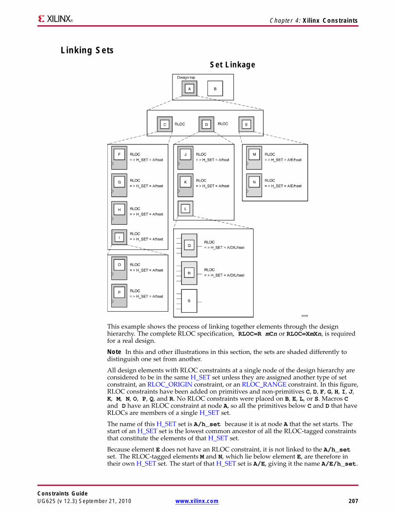
Chapter 4: Xilinx Constraints
Linking SetsSet Linkage
This example shows the process of linking together elements through the designhierarchy. The complete RLOC specification, RLOC=R mCn or RLOC=XmXn, is requiredfor a real design.
Note In this and other illustrations in this section, the sets are shaded differently todistinguish one set from another.
All design elements with RLOC constraints at a single node of the design hierarchy areconsidered to be in the same H_SET set unless they are assigned another type of setconstraint, an RLOC_ORIGIN constraint, or an RLOC_RANGE constraint. In this figure,RLOC constraints have been added on primitives and non-primitives C, D, F, G, H, I, J,K, M, N, O, P, Q, and R. No RLOC constraints were placed on B, E, L, or S. Macros Cand D have an RLOC constraint at node A, so all the primitives below C and D that haveRLOCs are members of a single H_SET set.
The name of this H_SET set is A/h_set because it is at node A that the set starts. Thestart of an H_SET set is the lowest common ancestor of all the RLOC-tagged constraintsthat constitute the elements of that H_SET set.
Because element E does not have an RLOC constraint, it is not linked to the A/h_setset. The RLOC-tagged elements M and N, which lie below element E, are therefore intheir own H_SET set. The start of that H_SET set is A/E, giving it the name A/E/h_set.
Constraints GuideUG625 (v 12.3) September 21, 2010 www.xilinx.com 207
Chapter 4: Xilinx Constraints
Similarly, the Q and R primitives are in their own H_SET set because they are not linkedthrough element L to any other design elements. The lowest common ancestor for theirH_SET set is L, which gives it the name A/D/L/h_set. After the flattening, NGDBuildattaches the sets to the primitives shown in the following tale.
Set PrimitivesH_SET=A/h_set F, G, H, O, P, J, K
H_SET=A/D/L/h_set Q, R
H_SET=A/E/h_set N
Consider a situation in which a set is created at the top of the design. There is no lowestcommon ancestor if macro A also has an RLOC constraint, since A is at the top of thedesign and has no ancestor. In this case, the base name h_set has no hierarchicallyqualified prefix, and the name of the H_SET set is simply h_set.
Modifying SetsThe RLOC constraint assigns a primitive an RLOC value (the row and column numberswith the optional extensions), specifies its membership in a set, and links togetherelements at different levels of the hierarchy. In the Three H_SET Sets example, the RLOCconstraint on macros C and D links together all the objects with RLOC constraints belowthem. An RLOC constraint is also used to modify the RLOC values of constraints belowit in the hierarchy. In other words, RLOC values of elements affect the RLOC values ofall other member elements of the same H_SET set that lie below the given elementin the design hierarchy.
When the design is flattened, the XY values of an RLOC constraint on an element areadded to the XY values of the RLOC constraints of the set members below it in thehierarchy. This feature allows you to modify existing RLOC values in submodulesand macros without changing the previously assigned RLOC values on the primitivesymbols.
The following sections describe the effect of the hierarchy on set modification.
Constraints Guide208 www.xilinx.com UG625 (v 12.3) September 21, 2010

Chapter 4: Xilinx Constraints
Adding RLOC Values Down the Hierarchy Example (Slice-BasedXY Designations)
This example illustrates the process of adding RLOC values down the hierarchy. Therow and column values between the parentheses show the addition function performedby the mapper. The italicized text prefixed by => is added by MAP during the designresolution process and replaces the original RLOC constraint that you added.
Constraints GuideUG625 (v 12.3) September 21, 2010 www.xilinx.com 209

Chapter 4: Xilinx Constraints
Modifying RLOC Values of Same Macro and Linking Togetheras One Set
The ability to modify RLOC values down the hierarchy is particularly valuable wheninstantiating the same macro more than once. Typically, macros are designed withRLOC constraints that are modified when the macro is instantiated.
This example is a variation of the previous example. The RLOC constraint on Inst1and Inst2 now link all the objects in one H_SET set.
Because the RLOC=X0Y0modifier on the Inst1macro does not affect the objects belowit, the mapper adds only the H_SET tag to the objects and leaves the RLOC values asthey are. However, the RLOC=X1Y0 modifier on the Inst2 macro causes MAP tochange the RLOC values on objects below it, as well as to add the H_SET tag, as shownin the italicized text.
Constraints Guide210 www.xilinx.com UG625 (v 12.3) September 21, 2010

Chapter 4: Xilinx Constraints
Separating Elements from H_SET SetsThe HU_SET (HU Set) constraint is a variation of the implicit H_SET (hierarchy set).HU_SET defines the start of a new set. Like H_SET, HU_SET is defined by the designhierarchy. However, you can use HU_SET to assign a user-defined name to the HU_SET.
This example demonstrates how HU_SET constraints designate elements as setmembers, break links between elements tagged with RLOC constraints in the hierarchyto separate them from H_SET sets, and generate names as identifiers of these sets.
The user-defined HU_SET constraint on E separates its underlying design elements,namely H, I, J, K, L, and M from the implicit H_SET=A/h_set that contains primitivemembers B, C, F, and G. The HU_SET set that is defined at E includes H, I, and L(through the element J).
The mapper hierarchically qualifies the name value “bar” on element E to be A/bar,since A is the lowest common ancestor for all the elements of the HU_SET set, andattaches it to the set member primitives H, I, and L. An HU_SET constraint on K startsanother set that includes M, which receives the HU_SET=A/E/bar constraint afterprocessing by the mapper.
The same name field is used for the two HU_SET constraints, but because they areattached to symbols at different levels of the hierarchy, they define two different sets.
Constraints GuideUG625 (v 12.3) September 21, 2010 www.xilinx.com 211

Chapter 4: Xilinx Constraints
Linking Two HU_SET Sets
This example shows how HU_SET constraints link elements in the same node togetherby naming them with the same identifier. Because of the same name (bar) on twoelements, D and E, the elements tagged with RLOC constraints below D and E becomepart of the same HU_SET.
Using RLOCs with Xilinx MacrosXilinx®-supplied flip-flop macros include an RLOC=R0C0 constraint on the underlyingprimitive, which allows you to attach an RLOC to the macro symbol. This symbol linksthe underlying primitive to the set that contains the macro symbol.
Simply attach an appropriate RLOC constraint to the instantiation of the Xilinx flip-flopmacro. The mapper adds the RLOC value that you specified to the underlying primitiveso that it has the desired value.
Constraints Guide212 www.xilinx.com UG625 (v 12.3) September 21, 2010

Chapter 4: Xilinx Constraints
In this example, the RLOC = R1C1 constraint is attached to the instantiation (Inst1) ofan example macro. It is added to the R0C0 value of the RLOC constraint on the flip-flopwithin the macro to obtain the new RLOC values.
If the RLOC=X1Y1 constraint is attached to Inst1 of a macro, the X0Y0 value of theRLOC constraint on the flip-flop within the macro would be used to obtain the newRLOC values.
If you do not put an RLOC constraint on the flip-flop macro symbol, the underlyingprimitive symbol is the lone member of a set. The mapper removes RLOC constraintsfrom a primitive that is the only member of a set or from a macro that has no RLOCobjects below it.
Syntax ExamplesThe following examples show how to use this constraint with particular tools ormethods. If a tool or method is not listed, you cannot use this constraint with it.
Schematic Syntax• Attach to an instance• Attribute Name
RLOC
• Attribute ValuesSee Constraint Syntax above.
VHDL SyntaxDeclare the VHDL constraint as follows:
attribute rloc: string;
Specify the VHDL constraint as follows:
attribute rloc of {component_name|entity_name| label_name}: {component|entity|label} is “[element]X mYn[ .extension]”;
For descriptions of valid values, see Guidelines for Specifying Relative Locations.
For more information about basic VHDL syntax, see VHDL Attributes.
Constraints GuideUG625 (v 12.3) September 21, 2010 www.xilinx.com 213

Chapter 4: Xilinx Constraints
The following code sample shows how to use RLOCs with a VHDL generate statement.The code is a simple example showing how to auto-generate the RLOCs for severalinstantiated FDEs. This methodology can be used with virtually any primitive.
Note The user must create the itoa function.
LEN:for i in 0 to bits-1 generateconstant row :natural:=((width-1)/2)-(i/2);constant column:natural:=0;constant slice:natural:=0;constant rloc_str : string := "R" & itoa(row) & "C" & itoa(column) & ".S" & itoa(slice);attribute RLOC of U1: label is rloc_str;beginU1: FDE port map (Q=> dd(j),D=> ff_d,C=> clk,CE =>lcl_en(en_idx));
end generate LEN;
Verilog SyntaxPlace the Verilog constraint immediately before the module or instantiation.
Specify the Verilog constraint as follows:
(* RLOC = “[element ]XmY n[.extension ]” *)
For descriptions of valid value, see Guidelines for Specifying Relative Locations inthis chapter.
For more information about basic Verilog syntax, see Verilog Attributes.
UCF and NCF SyntaxFor all FPGA devices, the following statement specifies that an instantiation of FF1 beplaced in a slice that is +4 X coordinates and +4 Y coordinates relative to the origin slice.
INST “/V2/design/FF1” RLOC=X4Y4;
XCF SyntaxFor Virtex®-4 and Virtex-5 devices:
BEGIN MODEL “entity_name ”
INST "instance_name " rloc=[element]XmYn [.extension] ;
END;
PlanAhead™ SyntaxFor more information about using the PlanAhead™ software to create constraints, seeFloorplanning the Design in the PlanAhead User Guide. See PlanAhead in this Guide forinformation about:• Defining placement constraints• Assigning placement constraints• Defining I/O pin configurations• Floorplanning and placement constraints
Guidelines for Specifying Relative LocationsThe slice-based coordinate system for assigning elements to relative location uses thefollowing general syntax.
RLOC=Xm Yn
Constraints Guide214 www.xilinx.com UG625 (v 12.3) September 21, 2010

Chapter 4: Xilinx Constraints
where
• m and n are the relative X axis (left/right) value and the relative Y axis (up/down)value, respectively.
• X and Y numbers can be zero or any positive or negative integer
Because the X and Y numbers in RLOC constraints define only the order and relationshipbetween design elements, and not their absolute die locations, their numbering caninclude negative numbers. Even though you can use any integer for RLOC constraints,Xilinx® recommends small integers for clarity and ease of use.
The absolute values of X and Y is not important in RLOC specifications, but rather theirrelative values or differences. For example, if design element A has an RLOC=X3Y4constraint and design element B has an RLOC=X6Y7 constraint, the absolute values ofX (3 and 6) are not important in themselves. However, the difference between them issignificant. In this case, 3 (6-3) specifies that the location of design element B is threeslices away from the location of design element A.
To capture this information, a normalization process is used and y coordinate-wise,element is 3 (7-4) slices above element A. In the example just given, normalizationreduces the RLOC on design element A to X0Y0, and the RLOC on design element Bto X3Y3.
In Spartan®-3 devices and higher and Virtex®-4 devices and higher, slices are numberedon an XY grid beginning in the lower left corner of the chip. X ascends in valuehorizontally to the right. Y ascends in value vertically up. RLOC constraints followthe Cartesian-based convention.
Constraints GuideUG625 (v 12.3) September 21, 2010 www.xilinx.com 215

Chapter 4: Xilinx Constraints
Different RLOC Specifications for Four Flip-Flop Primitives
This figure demonstrates the use of RLOC constraints. In diagram (a), four flip-flopprimitives named A, B, C, and D are assigned RLOC constraints. These RLOCconstraints require each flip-flop to be placed in a different slice with the slices stackedin the order shown: A below B, C, and D.
To place more than one of these flip-flop primitives per slice, specify the RLOCconstraints as shown in the diagram. The arrangement in the figure requires that A andB be placed in a single slice, and that C and D be placed in another slice immediately tothe right of the AB slice.
Relative Location RLOC SetsRelative Location (RLOC) constraints give order and structure to related designelements. This section describes RLOC sets, which are groups of related design elementsto which RLOC constraints have been applied. For example, the four flip-flops inDifferent RLOC Specifications for Four Flip-Flop Primitives are related by RLOCconstraints and form a set. Elements in a set are related by RLOC constraints to otherelements in the same set. Each member of a set must have an RLOC constraint, whichrelates it to other elements in the same set. You can create multiple sets, but a designelement can belong to only one set.
Sets can be defined explicitly through the use of a set parameter or implicitly throughthe structure of the design hierarchy.
Constraints Guide216 www.xilinx.com UG625 (v 12.3) September 21, 2010

Chapter 4: Xilinx Constraints
Four distinct types of rules are associated with each set.• Definition rules define the requirements for membership in a set.• Linkage rules specify how elements can be linked to other elements to form a single
set.• Modification rules dictate how to specify parameters that modify RLOC values of all
the members of the set.• Naming rules specify the nomenclature of sets.
These rules are discussed in the sections that follow.
The following sections discuss three different set constraints:• U_SET (U SET)• H_SET (H Set)• HU_SET (HU Set)
Elements must be tagged with both the RLOC constraint and one of these set constraintsto belong to a set.
U_SET (U SET)U_SET (U SET) allows you to group into a single set design elements with attachedRLOC constraints that are distributed throughout the design hierarchy. The letter U inthe name U_SET indicates that the set is user-defined.
U_SET allows you to group elements, even though they are not directly related by thedesign hierarchy. By attaching a U_SET constraint to design elements, you can explicitlydefine the members of a set.
The design elements tagged with a U_SET constraint can exist anywhere in thedesign hierarchy. They can be primitive or non-primitive symbols. When attached tonon-primitive symbols, the U_SET constraint propagates to all the primitive symbolswith RLOC constraints that are below it in the hierarchy.
The syntax of U_SET is:
U_SET=set_name
whereset_name is the user-specified identifier of the set
All design elements with RLOC constraints tagged with the same U_SET constraint namebelong to the same set. Names therefore must be unique among all the sets in the design.
H_SET (H Set)In contrast to U_SET, which you explicitly define by tagging design elements, H_SET (HSet) is defined implicitly through the design hierarchy. The combination of the designhierarchy and the presence of RLOC constraints on elements defines a hierarchicalset, or H_SET set.
You can not use H_SET to tag the design elements to indicate their set membership. Theset is defined automatically by the design hierarchy.
All design elements with RLOC constraints at a single node of the design hierarchy areconsidered to be in the same H_SET set unless they are tagged with another type ofset constraint such as Relative Location Origin (RLOC_ORIGIN) or Relative LocationRange (RLOC_RANGE). If you explicitly tag any element with RLOC_ORIGIN,RLOC_RANGE, U_SET, or HU_SET, it is removed from an H_SET set.
Constraints GuideUG625 (v 12.3) September 21, 2010 www.xilinx.com 217

Chapter 4: Xilinx Constraints
Most designs contain only H_SET constraints, since they are the underlying mechanismfor relationally placed macros. The Relative Location Origin (RLOC_ORIGIN) orRelative Location Range (RLOC_RANGE) constraints are discussed further in SetModifiers.
NGDBuild does the following:1. Recognizes the implicit H_SET set2. Derives its name or identifier3. Attaches the H_SET constraint to the correct members of the set4. Writes them to the output file
HU_SET (HU Set)HU_SET (HU Set) is a variation of the implicit H_SET. Like H_SET, HU_SET is definedby the design hierarchy. However, you can use the HU_SET constraint to assign auser-defined name to the HU_SET.
The syntax of HU_SET is:
HU_SET=set_name
where• set_name is the identifier of the set• set_name must be unique among all the sets in the design
This user-defined name is the base name of the HU_SET set. Like the H_SET set, inwhich the base name of h_set is prefixed by the hierarchical name of the lowestcommon ancestor of the set elements, the user-defined base name of an HU_SET set isprefixed by the hierarchical name of the lowest common ancestor of the set elements.
You must define the base names to ensure unique hierarchically qualified names forthe sets before the mapper resolves the design and attaches the hierarchical names asprefixes.
HU_SET defines the start of a new set. All design elements at the same node that have thesame user-defined value for the HU_SET constraint are members of the same HU_SETset. Along with the HU_SET constraint, elements can also have an RLOC constraint.
The presence of an RLOC constraint in an H_SET constraint links the element to allelements tagged with RLOC constraints above and below in the hierarchy. However, inthe case of an HU_SET constraint, the presence of an RLOC constraint along with theHU_SET constraint on a design element does not automatically link the element to otherelements with RLOC constraints at the same hierarchy level or above.
Constraints Guide218 www.xilinx.com UG625 (v 12.3) September 21, 2010

Chapter 4: Xilinx Constraints
Macro A Instantiated Twice
Note In this figure and the other related figures shown in the subsequent sections,the italicized text prefixed by => is added by NGDBuild during the design flatteningprocess. You add all other text.
This figure demonstrates a typical use of the implicit H_SET. The figure shows onlythe first RLOC portion of the constraint.
In a real design, the RLOC constraint must be specified completely with:
RLOC=R mCn
For Spartan®-3 devices and higher and Virtex®-4 devices and higher the RLOCconstraint must be specified completely with:
RLOC=XmYn
In this example, macro A is originally designed with RLOC constraints on four flip-flops:
• A
• B
• C
• D
The macro is then instantiated twice in the design:• Inst1
• Inst2
When the design is flattened, two different H_SET sets are recognized because twodistinct levels of hierarchy contain elements with RLOC constraints. NGDBuild createsand attaches the appropriate H_SET constraint to the set members:• H_SET=Inst1/h_set for the macro instantiated in Inst1• H_SET=Inst2/h_set for the macro instantiated in Inst2
The design implementation programs place each of the two sets individually as a unitwith relative ordering within each set specified by the RLOC constraints. However, thetwo sets are regarded to be completely independent of each other.
Constraints GuideUG625 (v 12.3) September 21, 2010 www.xilinx.com 219

Chapter 4: Xilinx Constraints
The name of the H_SET set is derived from the symbol or node in the hierarchy thatincludes all the RLOC elements. Inst1 is the node (instantiating macro) that includesthe four flip-flop elements with RLOC constraints shown on the left of the figure.Therefore, the name of this H_SET set is the hierarchically qualified name of Inst1followed by h_set.
The Inst1 symbol is considered the start of the H_SET, which gives a convenient handleto the entire H_SET and attaches constraints that modify the entire H_SET. Constraintsthat modify sets are discussed in the Save Net Flag (SAVE NET FLAG) constraint.
This figure demonstrates the simplest use of a set that is defined and confined to a singlelevel of hierarchy. Through linkage and modification, you can also create an H_SET setthat is linked through two or more levels of hierarchy.
Linkage allows you to link elements through the hierarchy into a single set. On theother hand, modification allows you to modify RLOC values of the members of a setthrough the hierarchy.
RLOC Set SummaryThe following table summarizes the RLOC set types and the constraints that identifymembers of these sets.
Summary of Set TypesType Definition Naming Linkage ModificationU_SET= name All elements with
the same user-taggedU_SET constraintvalue are members ofthe same U_SET set.
The name of theset is the same asthe user-definedname withoutany hierarchicalqualification.
U_SET links elementsto all other elementswith the samevalue for the U_SETconstraint.
U_SET is modifiedby applyingRLOC_ORIGINor RLOC_RANGEconstraints on,at most, oneof the U_SETconstraint-taggedelements.
HU_SET= name All elements with thesame hierarchicallyqualified name aremembers of the sameset.
The lowest commonancestor of themembers is prefixed tothe user-defined nameto obtain the name ofthe set.
HU_SET links to otherelements at the samenode with the sameHU_SET constraintvalue. It links toelements with RLOCconstraints below.
The start of the setis made up of theelements on thesame node thatare tagged withthe same HU_SETconstraint value. ARLOC_ORIGIN ora RLOC_RANGEconstraint can beapplied to, at most,one of these startelements of anHU_SET set.
Constraints Guide220 www.xilinx.com UG625 (v 12.3) September 21, 2010

Chapter 4: Xilinx Constraints
RLOC_ORIGIN (Relative Location Origin)The RLOC_ORIGIN (Relative Location Origin) constraint:• Is a placement constraint.• Fixes the members of a set at exact die locations.• Must specify a single location, not a range or a list of several locations.
For more information, see Set Modifiers in the Relative Location (RLOC) constraint.• Is required for a set that includes BUFT symbols.• Cannot be attached to a BUFT instance.
Architecture SupportApplies to FPGA devices. Does not apply to CPLD devices.
Applicable ElementsInstances or macros that are members of sets
Propagation RulesRLOC_ORIGIN is a macro constraint and any attachment to a net is illegal.
When RLOC_ORIGIN is used in conjunction with an implicit H_SET, it must be placedon the element that is the start of the H_SET set, that is, on the lowest common ancestorof all the members of the set.
If you apply RLOC_ORIGIN to an HU_SET constraint, place it on the element at thestart of the HU_SET set, that is, on an element with the HU_SET constraint.
However, since there could be several elements linked together with the HU_SETconstraint at the same node, the RLOC_ORIGIN constraint can be applied to only one ofthese elements to prevent more than one RLOC_ORIGIN constraint from being appliedto the HU_SET set.
Similarly, when used with a U_SET constraint, the RLOC_ORIGIN constraint can beplaced on only one element with the U_SET constraint. If you attach the RLOC_ORIGINconstraint to an element that has only an RLOC constraint, the membership of thatelement in any set is removed, and the element is considered the start of a new H_SETset with the specified RLOC_ORIGIN constraint attached to the newly created set.
Constraint SyntaxTo specify a single origin for an RLOC set, use the following syntax, which is equivalentto placing an RLOC_ORIGIN constraint on the schematic.
set_name RLOC_ORIGIN=Xm Yn
where• set_name can be the name of any type of RLOC set:
– U_SET– HU_SET– system-generated H_SET
• The origin itself is expressed as an X and Y value representing the location of theelements at RLOC=X0Y0
Constraints GuideUG625 (v 12.3) September 21, 2010 www.xilinx.com 221

Chapter 4: Xilinx Constraints
Syntax ExamplesThe following examples show how to use this constraint with particular tools ormethods. If a tool or method is not listed, you cannot use this constraint with it.
Schematic Syntax• Attach to an instance that is a member of a set• Attribute Name
RLOC_ORIGIN
• Attribute ValuesFor a list of the constraint values, see the UCF and NCF Syntax section below.
VHDL SyntaxDeclare the VHDL constraint as follows:
attribute rloc_origin: string;
Specify the VHDL constraint as follows:
attribute rloc_origin of {component_name |entity_name|label_name} :{component|entity |label} is “ value”;
For Spartan®-3, Spartan-3A, Spartan-3E, Virtex®-4 and Virtex-5 devices, value is X mYn.
For a list of the constraint values, see the UCF and NCF Syntax section below.
For more information about basic VHDL syntax, see VHDL Attributes.
Verilog SyntaxPlace the Verilog constraint immediately before the module or instantiation.
Specify the Verilog constraint as follows:
(* RLOC_ORIGIN = “ value” *)
For Spartan-3, Spartan-3A, Spartan-3E, Virtex-4 and Virtex-5 devices, value is X mYn.
For a list of the constraint values, see the UCF and NCF Syntax section below.
For more information about basic Verilog syntax, see Verilog Attributes.
UCF and NCF Syntax for Architectures Using Slice-Based XY CoordinatesThis section applies to Spartan-3, Spartan-3A, Spartan-3E, Virtex-4, and Virtex-5 devices.
RLOC_ORIGIN=X mYn
wherem and n are positive or negative integers (including zero) representing relative X and Ycoordinates, respectively
The following statement specifies that an instantiation of FF1, which is a member of aset, be placed in the slice at X4Y4 relative to FF1.
INST “/archive/designs/FF1” RLOC_ORIGIN=X4Y4;
For example, if RLOC=X0Y2 for FF1, then the instantiation of FF1 is placed in the slicethat is:• 0 rows to the right of X4• 2 rows up from Y4 (X4Y6)
Constraints Guide222 www.xilinx.com UG625 (v 12.3) September 21, 2010

Chapter 4: Xilinx Constraints
PlanAhead™ SyntaxFor more information about using the PlanAhead™ software to create constraints, seeFloorplanning the Design in the PlanAhead User Guide. See PlanAhead in this Guide forinformation about:• Defining placement constraints• Assigning placement constraints• Defining I/O pin configurations• Floorplanning and placement constraints
RLOC_RANGE (Relative Location Range)The RLOC_RANGE (Relative Location Range) constraint:• Is a placement constraint.• Is similar to RLOC_ORIGIN except that it limits the members of a set to a certain
range on the die. The range or list of locations is meant to apply to all applicableelements with RLOCs, not just to the origin of the set
Architecture SupportApplies to FPGA devices. Does not apply to CPLD devices.
Applicable ElementsInstances or macros that are members of sets
Propagation RulesRLOC_RANGE is a macro constraint and any attachment to a net is illegal.
The bounding rectangle applies to all elements in a relationally placed macro, not justto the origin of the set.
The values of the RLOC_RANGE constraint are not simply added to the RLOC values ofthe elements. In fact, the RLOC_RANGE constraint does not change the values of theRLOC constraints on underlying elements. It is an additional constraint that is attachedautomatically by the mapper to every member of a set.
The RLOC_RANGE constraint is attached to design elements in exactly the sameway as the RLOC_ORIGIN constraint. The values of the RLOC_RANGE constraint,like RLOC_ORIGIN values, must be non-zero positive numbers since they directlycorrespond to die locations.
If a particular RLOC set is constrained by an RLOC_ORIGIN or an RLOC_RANGEconstraint in the design netlist and is also constrained in the User Constraints File (UCF)file, the UCF constraint overrides the netlist constraint.
Constraint SyntaxRLOC_RANGE=Xm1 Yn1:X m2Yn2
wherethe relative X values (m1 andm2 ) and Y values (n1 and n2) can be:– non-zero positive numbers– the wildcard (*) character
Constraints GuideUG625 (v 12.3) September 21, 2010 www.xilinx.com 223

Chapter 4: Xilinx Constraints
This syntax allows for three kinds of range specifications:• Xm1Yn1:Xm2 Yn2
A rectangular region bounded by the corners Xm1Yn1 and Xm2 Yn2
• X*Yn1:X*Ym2
The region on the Y-axis between n1 and n2 (any X value)• Xm1Y*:Xm2
A region on the X-axis between m1 and m2 (any Y value)
For the second and third kinds of specifications with wildcards, applying the wildcardcharacter (*) differently on either side of the separator colon creates an error. Forexample, specifying X*Y1:X2Y* is an error since the wildcard asterisk is applied to theX value on one side and to the Y value on the other side of the separator colon.
To specify a range, use the following syntax, which is equivalent to placing anRLOC_RANGE constraint on the schematic.
set_name RLOC_RANGE=X m1Yn1 :Xm2Y n2
The range identifies a rectangular area. You can substitute a wildcard (*) character foreither the X value or the Y value of both corners of the range.
Syntax ExamplesThe following examples show how to use this constraint with particular tools ormethods. If a tool or method is not listed, you cannot use this constraint with it.
Schematic Syntax• Attach to an instance that is a member of a set• Attribute Name
RLOC_RANGE
• Attribute Values– positive integers (including zero)– the wildcard (*) character
VHDL SyntaxDeclare the VHDL constraint as follows:
attribute rloc_range: string;
Specify the VHDL constraint as follows:
attribute rloc_range of {component_name|entity_name|label_name}:{component|entity|label} is “value”;
For Spartan®-3, Spartan-3A, Spartan-3E, Virtex®-4 and Virtex-5 devices value is:
Xm1Yn1:Xm2Yn2
For a list of the constraint values, see the UCF and NCF Syntax section below.
For more information about basic VHDL syntax, see VHDL Attributes.
Verilog SyntaxPlace the Verilog constraint immediately before the module or instantiation.
Specify the Verilog constraint as follows:
(* RLOC_RANGE = “value” *)
For Spartan-3, Spartan-3A, Spartan-3E, Virtex-4 and Virtex-5 devices, value is:
Constraints Guide224 www.xilinx.com UG625 (v 12.3) September 21, 2010

Chapter 4: Xilinx Constraints
Xm1Yn1:Xm2Yn2
For a list of the constraint values, see the UCF and NCF Syntax section below.
For more information about basic Verilog syntax, see Verilog Attributes.
UCF and NCF SyntaxThis section is applicable Spartan-3 devices and up, and Virtex-4 devices and up.
RLOC_RANGE=Xm1Yn1:Xm2Yn2
wherethe relative X values (m1 and m2) and Y values (n1 and n2) can be:– positive integers (including zero)– the wildcard (*) character
The following statement specifies that an instantiation of the macro MACRO4 be placedrelative to other members of the set within a region that is bounded by:• X4Y4 in the lower left corner• X10Y10 in the upper right corner
INST “/archive/designs/MACRO4” RLOC_RANGE=X4Y4:X10Y10;
XCF SyntaxMODEL “entity_name” rloc_range=value;
BEGIN MODEL “entity_name”
INST "instance_name" rloc_range=value;
END;
SAVE NET FLAG (Save Net Flag)The SAVE NET FLAG (Save Net Flag) constraint:• Is a basic mapping constraint.• When attached to nets or signals, affects the mapping, placement, and routing of the
design by preventing the removal of unconnected signals.• Prevents the removal of loadless or driverless signals.
– For loadless signals, SAVE NET FLAG acts as a dummy OBUF load connectedto the signal.
– For driverless signals, SAVE NET FLAG acts as a dummy IBUF driver connectedto the signal.
• Can be abbreviated as S NET FLAG.
If you do not have SAVE NET FLAG on a net, any signal that cannot be observed orcontrolled via a path to an I/O primitive is removed.
SAVE NET FLAG may prevent the trimming of logic connected to the signal.
Architecture SupportApplies to FPGA devices. Does not apply to CPLD devices.
Constraints GuideUG625 (v 12.3) September 21, 2010 www.xilinx.com 225

Chapter 4: Xilinx Constraints
Applicable Elements• Nets• Signals
Propagation RulesThis constraint:• Is a net or signal constraint. Any attachment to a design element is illegal• Prevents the removal of unconnected signals. If you do not have the S constraint on
a net, any signal not connected to logic or an I/O primitive is removed.
SAVE NET FLAG SyntaxThe following examples show how to use this constraint with particular tools ormethods. If a tool or method is not listed, you cannot use this constraint with it.
Schematic Syntax• Attach to a net or signal• Attribute Name
S
• Attribute Values– TRUE
– FALSE
VHDL SyntaxDeclare the VHDL constraint as follows:
attribute S: string;
Specify the VHDL constraint as follows:
attribute S of signal_name : signal is ”{YES|NO|TRUE|FALSE }”;
For more information about basic VHDL syntax, see VHDL Attributes.
Verilog SyntaxPlace the Verilog constraint immediately before the module or instantiation.
Specify the Verilog constraint as follows:
(* S = {YES|NO|TRUE|FALSE} *)
For more information about basic Verilog syntax, see Verilog Attributes.
UCF and NCF SyntaxThe following statement specifies that the net or signal named $SIG_9 should not beremoved.
NET $SIG_9 S;
XCF SyntaxBEGIN MODEL entity_name
NET "signal_name" s=true;
END;
Constraints Guide226 www.xilinx.com UG625 (v 12.3) September 21, 2010

Chapter 4: Xilinx Constraints
SCHMITT_TRIGGER (Schmitt Trigger)The SCHMITT_TRIGGER (Schmitt Trigger) constraint:• Causes the attached input pad to be configured with Schmitt Trigger (hysteresis).• Applies to any input pad in the design.
Architecture SupportApplies to CoolRunner™-II devices only.
Applicable ElementsAll input pads and pad nets
Propagation RulesThis constraint is a net or signal constraint. Any attachment to a macro, entity, ormodule is illegal.
Syntax ExamplesThe following examples show how to use this constraint with particular tools ormethods. If a tool or method is not listed, you cannot use this constraint with it.
Schematic Syntax• Attach to a net• Attribute Name
SCHMITT_TRIGGER
• Attribute ValuesTRUE
FALSE
VHDL SyntaxDeclare the VHDL constraint as follows:
attribute SCHMITT_TRIGGER: string;
Specify the VHDL constraint as follows:
attribute SCHMITT_TRIGGER of signal_name : signal is “{TRUE|FALSE}”;
For more information about basic VHDL syntax, see VHDL Attributes.
Verilog SyntaxPlace the Verilog constraint immediately before the module or instantiation.
Specify the Verilog constraint as follows:
(* SCHMITT_TRIGGER = “{TRUE|FALSE}” *)
For more information about basic Verilog syntax, see Verilog Attributes.
UCF and NCF SyntaxNET “mysignal” SCHMITT_TRIGGER;
Constraints GuideUG625 (v 12.3) September 21, 2010 www.xilinx.com 227

Chapter 4: Xilinx Constraints
XCF SyntaxBEGIN MODEL “entity_name ”
NET "signal_name" SCHMITT_TRIGGER=true;
END;
SIM Collision Check (SIM_COLLISION_CHECK)The SIM Collision Check (SIM_COLLISION_CHECK) constraint is used to specifysimulation model behavior when a read/write collision occurs on a memory locationof Block RAM.
Architecture SupportThis constraint applies to Virtex®-4 devices and higher only. It does not apply toSpartan® devices or to CPLD devices.
Applicable ElementsBlock RAM primitive elements
Propagation RulesIt is illegal to attach this constraint to a net or signal.
Syntax ExamplesThe following examples show how to use this constraint with particular tools ormethods. If a tool or method is not listed, you cannot use this constraint with it.
ValuesThis constraint has the following values:
• ALLGenerates both a WARNING message and X’s on the output during simulation.
• NONEIgnores collisions leading to unpredictable results during simulation.
• WARNING_ONLYGenerates a WARNING message during simulation if there is a read/write collisionon a memory location in the Virtex-4 block RAM memory,
• GENERATE_X_ONLYGenerates X’s on the outputs during simulation.
Schematic Syntax• Attached to a block RAM primitive• Attribute Name
SIM_COLLISION_CHECK• Attribute Values
See Values section above.
Constraints Guide228 www.xilinx.com UG625 (v 12.3) September 21, 2010

Chapter 4: Xilinx Constraints
VHDL SyntaxDeclare the VHDL constraint as follows:
attribute sim_collision_check: string;
Specify the VHDL constraint as follows:
attribute sim_collision_check of {component_name|label_name}: {component|label} is“sim_collision_check_value”;
For more information about basic VHDL syntax, see VHDL Attributes.
Verilog SyntaxPlace the Verilog constraint immediately before the module or instantiation.
Specify the Verilog constraint as follows:
// synthesis attribute sim_collision_check [of] {module_name|instance_name} [is]“sim_collision_check_value”;
For more information about basic Verilog syntax, see Verilog Attributes.
UCF and NCF SyntaxThe following statement sets the SIM_COLLISION_CHECK constraint for aninstantiation of an I/O primitive element y2.
INST “$1187/y2SIM_COLLISION_CHECK={WARNING_ONLY|GENERATE_X_ONLY|ALL|NONE};
SLEW (Slew)The SLEW (Slew) constraint:• Defines the slew rate (rate of transition) behavior of each individual output to the
device.• May be placed on any output or bi-directional port to specify the port slew rate to be:
– SLOW (default)– FAST
– QUIETIO (Spartan®-3A devices)Use the slowest SLEW attribute available to the device while still allowing applicableI/O timing to be met in order to minimize any possible signal integrity issues.
Architecture SupportApplies to all FPGA devices and all CPLD devices.
Applicable ElementsOutput primitives, output pads, bidirectional pads.
You can also attach SLEW to the net connected to the pad component in a UserConstraints File (UCF). NGCBuild transfers SLEW from the net to the pad instance inthe NGD file so that it can be processed by the mapper. Use the following syntax:
NET “net_name” slew={FAST|SLOW};
Propagation RulesSLEW should only be placed on a top-level output or bi-directional port.
Constraints GuideUG625 (v 12.3) September 21, 2010 www.xilinx.com 229

Chapter 4: Xilinx Constraints
SyntaxThe following examples show how to use this constraint with particular tools ormethods. If a tool or method is not listed, you cannot use this constraint with it.
ValuesThis constraint has the following values:
• FAST• SLOW• QUIETIO
Spartan-3A devices only
Schematic SyntaxSpecify a new attribute to an output port, or bi-directional port:• Attribute Name
SLEW
• Attribute ValuesSee Values section above.
VHDL SyntaxBefore using SLEW, declare it with the following syntax placed after the architecturedeclaration, but before the begin statement in the top-level VHDL file:
attribute SLEW: string;
Specify the VHDL constraint as follows:
attribute SLEW of {top_level_port_name}: signal is " value";
VHDL Syntax Exampleentity top is
port (FAST_OUT: out std_logic);
end top;
architecture MY_DESIGN of top is
attribute SLEW: string;
attribute SLEW of FAST_OUT: signal is "FAST";
begin
For more information on basic VHDL syntax, see VHDL Attributes.
Verilog SyntaxPlace the following attribute specification before the port declaration in the top-levelVerilog code:
(* SLEW="value" *)
Verilog Syntax Examplemodule top (
(* SLEW="FAST" *) output FAST_OUT
);
Constraints Guide230 www.xilinx.com UG625 (v 12.3) September 21, 2010

Chapter 4: Xilinx Constraints
For more information about basic Verilog syntax, see Verilog Attributes.
User Constraints File (UCF) and Netlist Constraints File (NCF) SyntaxPlaced on output or bi-directional port:
NET "top_level_port_name" SLEW="
value";
UCF and NCF Syntax ExampleNET "FAST_OUT" SLEW="FAST";
PlanAhead™ SyntaxFor more information about using the PlanAhead™ software to create constraints, seeFloorplanning the Design in the PlanAhead User Guide. See PlanAhead in this Guide forinformation about:• Defining placement constraints• Assigning placement constraints• Defining I/O pin configurations• Floorplanning and placement constraints
PACE SyntaxTo set SLEW in PACE, select the pin value in the Design Objects window.
PACE is supported for CPLD devices only.
SLOW (Slow)The SLOW (Slow) constraint:• Is a basic fitter constraint• Enables the slew rate limited control
Architecture SupportApplies to all FPGA devices and all CPLD devices.
Applicable Elements• Output primitives• Output pads• Bidirectional pads
You can also attach SLOW to the net connected to the pad component in a UserConstraints File (UCF). NGCBuild transfers SLOW from the net to the pad instance inthe Native Generic Database (NGD) file so that it can be processed by the mapper.
Use the following UCF syntax:
NET “net_name” SLOW;
Propagation RulesSLOW is illegal when attached to a net except when the net is connected to a pad. Inthis case, SLOW is treated as attached to the pad instance.
Constraints GuideUG625 (v 12.3) September 21, 2010 www.xilinx.com 231

Chapter 4: Xilinx Constraints
When attached to a design element, SLOW propagates to all applicable elements inthe hierarchy within the design element.
SyntaxThe following examples show how to use this constraint with particular tools ormethods. If a tool or method is not listed, you cannot use this constraint with it.
Schematic Syntax• Attach to a valid instance• Attribute Name
SLOW
• Attribute Values– TRUE
– FALSE
VHDL SyntaxDeclare the VHDL constraint as follows:
attribute SLOW : string;
Specify the VHDL constraint as follows:
attribute SLOW of {signal_name|entity_name} : {signal|entity} is “{TRUE|FALSE}”;
For more information about basic VHDL syntax, see VHDL Attributes.
Verilog SyntaxPlace the Verilog constraint immediately before the module or instantiation.
Specify the Verilog constraint as follows:
(* SLOW = “{TRUE|FALSE}” *)
For more information about basic Verilog syntax, see Verilog Attributes.
UCF and NCF SyntaxThe following statement establishes a slow slew rate for an instantiation of the elementy2.
INST “$1I87/y2” SLOW;
The following statement establishes a slow slew rate for the pad to which net1 isconnected.
NET “net1” SLOW;
PlanAhead™ SyntaxFor more information about using the PlanAhead™ software to create constraints, seeFloorplanning the Design in the PlanAhead User Guide. See PlanAhead in this Guide forinformation about:• Defining placement constraints• Assigning placement constraints• Defining I/O pin configurations• Floorplanning and placement constraints
Constraints Guide232 www.xilinx.com UG625 (v 12.3) September 21, 2010

Chapter 4: Xilinx Constraints
STEPPING (Stepping)The STEPPING (Stepping) constraint is assigned a value that matches the step levelmarking on the silicon. The step level identifies specific device capabilities. Xilinx®recommends that the step level be set for the design using STEPPING. Otherwise, thesoftware uses a default target device.
For more information on STEPPING, see Xilinx Answer Record 20947, Stepping FAQs.
Architecture Support• CoolRunner™-II• Spartan®-3A, Spartan-3E, Virtex®-4, Virtex-5
Applicable ElementsThe STEPPING attribute is a global CONFIG constraint and is not attached to anyinstance or signal name.
Propagation RulesApplies to the entire design.
Syntax ExamplesThe following examples show how to use this constraint with particular tools ormethods. If a tool or method is not listed, you cannot use this constraint with it.
UCF SyntaxCONFIG STEPPING=”n”;
where
n is the target stepping level (ES, SCD1, 1, 2, 3, ...)
UCF Syntax ExampleCONFIG STEPPING="1";
SUSPEND (Suspend)The SUSPEND (Suspend) constraint:• Defines the behavior of each individual output when the FPGA device is placed in
the SUSPEND power-reduction mode.• May be placed on any output or bi-directional port to specify the port to be:
– tristated (3STATE) OR– pulled high (3STATE_PULLUP) or low (3STATE_PULLDOWN) OR– driven to the last value (3STATE_KEEPER or DRIVE_LAST_VALUE)
• Has a default value of 3STATE
Architecture SupportApplies to Spartan®-3A and Spartan-6 devices only.
Constraints GuideUG625 (v 12.3) September 21, 2010 www.xilinx.com 233

Chapter 4: Xilinx Constraints
Applicable ElementsPlace this constraint only on a top-level output or bi-directional port targeting aSpartan-3A device or a Spartan-6 device.
Propagation RulesPlace this constraint only on a top-level output or bi-directional port.
Syntax ExamplesThe following examples show how to use this constraint with particular tools ormethods. If a tool or method is not listed, you cannot use this constraint with it.
ValuesThis constraint has the following values:• DRIVE_LAST_VALUE• 3STATE• 3STATE_PULLUP• 3STATE_PULLDOWN• 3STATE_KEEPER
Schematic SyntaxSpecify a new attribute to an output port or bidirectional port:• Attribute Name
SUSPEND• Attribute Values
See Values section above.
VHDL SyntaxBefore using this constraint, declare it with the following syntax placed after thearchitecture declaration but before the begin statement in the top-level VHDL file:
attribute SUSPEND: string;
After the constraint has been declared, specify the VHDL constraint as follows:
attribute SUSPEND of {top_level_port_name} : signal is "value";
Example:
entity top isport (STATUS: out std_logic);end top;architecture MY_DESIGN of top isattribute SUSPEND: string;attribute SUSPEND of STATUS: signal is "DRIVE_LAST_VALUE";begin
For more information about basic VHDL syntax, see VHDL Attributes.
Verilog SyntaxPlace the following attribute specification before the port declaration in the top-levelVerilog code:
(* SUSPEND="value" *)
Example:
module top ( (* SUSPEND="DRIVE_LAST_VALUE" *) output STATUS );
Constraints Guide234 www.xilinx.com UG625 (v 12.3) September 21, 2010

Chapter 4: Xilinx Constraints
For more information about basic Verilog syntax, see Verilog Attributes.
UCF and NCF SyntaxPlaced on an output or bi-directional port:
NET "top_level_port_name" SUSPEND="value";
Example:
NET "STATUS" SUSPEND="DRIVE_LAST_VALUE";
PACE SyntaxTo set this constraint from the Pinout and Area Constraints Editor (PACE), select theappropriate pin value from the Design Objects window.
SYSTEM_JITTER (System Jitter)The SYSTEM_JITTER (System Jitter) constraint:
• Specifies the system jitter of the design.
• Depends on design conditions such as:
– the number of flip-flops changing at one time
– the number of I/Os changing
• Applies globally to all clocks in the design.
• Is combined with the INPUT_JITTER keyword on the PERIOD constraint, as wellas any jitter or phase error in the clock network, to generate the Clock Uncertaintyvalue that is shown in the timing report.
Architecture SupportApplies to FPGA devices. Does not apply to CPLD devices.
Applicable ElementsApplies to the entire design.
Propagation RulesNot applicable
Syntax ExamplesThe following examples show how to use this constraint with particular tools ormethods. If a tool or method is not listed, you cannot use this constraint with it.
ValuesThis constraint has the following values:
value is a numerical value. The default is ps.
Constraints GuideUG625 (v 12.3) September 21, 2010 www.xilinx.com 235

Chapter 4: Xilinx Constraints
Schematic Syntax• Attach to a valid instance
• Attribute Name
SYSTEM_JITTER
• Attribute Values
See Values section above.
VHDL SyntaxDeclare the VHDL constraint as follows:
attribute SYSTEM_JITTER: string;
Specify the VHDL constraint as follows:
attribute SYSTEM_JITTER of {component_name | signal_name | entity_name |label_name}: {component | signal | entity| label} is “value ps”;
For more information about basic VHDL syntax, see VHDL Attributes.
Verilog SyntaxPlace the Verilog constraint immediately before the module or instantiation.
Specify the Verilog constraint as follows:
(* SYSTEM_JITTER = “value ps” *)
For more information about basic Verilog syntax, see Verilog Attributes.
UCF and NCF SyntaxSYSTEM_JITTER= value ps;
XCF SyntaxMODEL “entity_name ” SYSTEM_JITTER = value ps;
TEMPERATURE (Temperature)The TEMPERATURE (Temperature) constraint:
• Is a timing constraint.
• Allows the specification of the operating junction temperature.
• Provides a means of using device delay characteristics based on the specifiedtemperature.
Prorating is a scaling operation on existing speed file delays and is applied globally toall delays. Newer devices may not support TEMPERATURE prorating until the timinginformation (speed files) are marked as production status.
Each architecture has its own specific range of valid operating temperatures. If theentered temperature does not fall within the supported range, TEMPERATURE isignored and an architecture-specific worst-case value is used instead. Also note that theerror message for this condition does not appear until static timing.
Constraints Guide236 www.xilinx.com UG625 (v 12.3) September 21, 2010

Chapter 4: Xilinx Constraints
Architecture Support• Spartan®-3A• Spartan-3E• Virtex®-4• Virtex-5
Applicable ElementsApplies globally to the entire design.
Propagation RulesThis constraint is a design element constraint. Any attachment to a net is illegal.
SyntaxThe following examples show how to use this constraint with particular tools ormethods. If a tool or method is not listed, you cannot use this constraint with it.
UCF and NCF SyntaxTEMPERATURE=value [C |F| K];
where
value• is a real number specifying the temperature• C, K, and F are the temperature units
– F is degrees Fahrenheit– K is degrees Kelvin– C is degrees Celsius (default)
The following statement specifies that the analysis for everything relating to speed filedelays assumes a junction temperature of 25 degrees Celsius.
TEMPERATURE=25 C;
Constraints Editor SyntaxFor information on setting constraints in Constraints Editor, including syntax, see theConstraints Editor Help.
TIG (Timing Ignore)The TIG (Timing Ignore) constraint:• Is a timing constraint and a synthesis constraint.• Causes paths that fan forward from the point of application (of TIG) to be treated as
if they do not exist (for the purposes of timing analysis) during implementation.• Can be applied relative to a specific timing specification.• Can have any of the following values:
– Empty (global TIG that blocks all paths)– A single TSid to block– A comma separated list of TSids to block, for example
• Is fully supported by XST.
Constraints GuideUG625 (v 12.3) September 21, 2010 www.xilinx.com 237
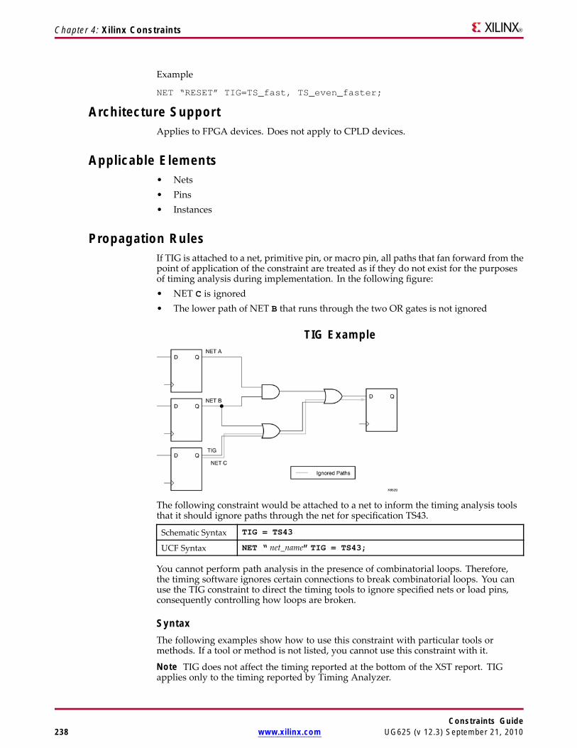
Chapter 4: Xilinx Constraints
Example
NET “RESET” TIG=TS_fast, TS_even_faster;
Architecture SupportApplies to FPGA devices. Does not apply to CPLD devices.
Applicable Elements• Nets• Pins• Instances
Propagation RulesIf TIG is attached to a net, primitive pin, or macro pin, all paths that fan forward from thepoint of application of the constraint are treated as if they do not exist for the purposesof timing analysis during implementation. In the following figure:• NET C is ignored• The lower path of NET B that runs through the two OR gates is not ignored
TIG Example
The following constraint would be attached to a net to inform the timing analysis toolsthat it should ignore paths through the net for specification TS43.
Schematic Syntax TIG = TS43
UCF Syntax NET “ net_name” TIG = TS43;
You cannot perform path analysis in the presence of combinatorial loops. Therefore,the timing software ignores certain connections to break combinatorial loops. You canuse the TIG constraint to direct the timing tools to ignore specified nets or load pins,consequently controlling how loops are broken.
SyntaxThe following examples show how to use this constraint with particular tools ormethods. If a tool or method is not listed, you cannot use this constraint with it.
Note TIG does not affect the timing reported at the bottom of the XST report. TIGapplies only to the timing reported by Timing Analyzer.
Constraints Guide238 www.xilinx.com UG625 (v 12.3) September 21, 2010

Chapter 4: Xilinx Constraints
Schematic Syntax• Attach to a net or pin• Attribute Name
TIG• Attribute Values
value
UCF and NCF SyntaxNET “ net_name” TIG;
PIN “ff_inst.RST” TIG=TS_1;
INST “instance_name ” TIG=TS_2;
TIG=TS identifier1 . . . TS identifiern
identifier refers to a timing specification that should be ignored
When attached to an instance, TIG is pushed to the output pins of that instance. Whenattached to a net, TIG pushes to the drive pin of the net. When attached to a pin, TIGapplies to the pin.
The following statement specifies that the timing specifications TS_fast andTS_even_faster is ignored on all paths fanning forward from the net RESET.
NET “RESET” TIG=TS_fast, TS_even_faster;
XST Constraint File (XCF) SyntaxThe XST Constraint File (XCF) syntax is the same as the User Constraints File (UCF)syntax.
XST fully supports the TIG constraint. TIG can be applied to the nets, situated in theCORE files:• Electronic Data Interchange Format (EDIF)• Native Generic Database (NGD)
Constraints Editor SyntaxFor information on Constraints Editor and Constraints Editor syntax in ISE® DesignSuite, see the ISE Design Suite Help.
PlanAhead™ SyntaxFor more information about using the PlanAhead™ software to create constraints, seeFloorplanning the Design in the PlanAhead User Guide. See PlanAhead in this Guide forinformation about:• Defining placement constraints• Assigning placement constraints• Defining I/O pin configurations• Floorplanning and placement constraints
Physical Constraints File (PCF) SyntaxThe basic Physical Constraints File (PCF) syntax is:
item TIG;
item TIG =;
item TIG = TSidentifier ;
Constraints GuideUG625 (v 12.3) September 21, 2010 www.xilinx.com 239
Chapter 4: Xilinx Constraints
item is one of the following:• PIN name• PATH name• path specification• NET name• TIMEGRP name• BEL name• COMP name• MACRO name
TIMEGRP (Timing Group)The TIMEGRP (Timing Group) constraint:• Uses the Timing Name (TNM) identifier to group design elements together for
timing analysis.• Allows you to:
– Define groups in terms of other groups– Create a group that is a combination of existing groups– Place TIMEGRP constraints in a User Constraints File (UCF) or a Netlist
Constraints File (NCF)
Architecture SupportApplies to all FPGA devices and all CPLD devices.
Applicable Elements• Design elements• Nets
Propagation RulesApplies to all elements or nets within the group.
SyntaxThe following examples show how to use this constraint with particular tools ormethods. If a tool or method is not listed, you cannot use this constraint with it.
Combining Multiple Groups into OneYou can define a group by combining other groups.
Multiple Groups UCF Syntax Example OneThe following syntax example illustrates the simple combining of two groups.
TIMEGRP “big_group”="small_group” “medium_group”;
In this syntax example, small_group and medium_group are existing groups defined usinga TNM or TIMEGRP attribute.
Constraints Guide240 www.xilinx.com UG625 (v 12.3) September 21, 2010

Chapter 4: Xilinx Constraints
Multiple Groups UCF Syntax Example TwoA circular definition, as shown below, causes an error when you run your designthrough NGCBuild:
TIMEGRP “many_ffs”=”ffs1” “ffs2”;
TIMEGRP “ffs1”=”many_ffs” “ffs3”;
Creating Groups by ExclusionYou can define a group that includes all elements of one group except the elements thatbelong to another group, as illustrated by the following syntax examples:
Groups by Exclusion UCF Syntax Example OneTIMEGRP “group1”="group2" EXCEPT “group3”;
where• group1 represents the group being defined. It contains all of the elements in group2
except those that are also in group3.• group2 and group3 can be a:
– valid TNM– predefined group– TIMEGRP attribute
Groups by Exclusion UCF Syntax Example TwoAs illustrated by the following example, you can specify multiple groups to includeor exclude when creating the new group.
TIMEGRP “group1”=” “group2” “group3” EXCEPT "group4" "group5";
The example defines a group1 that includes the members of group2 and group3, except forthose members that are part of group4 or group5. All of the groups before the keywordEXCEPT are included, and all of the groups after the keyword are excluded.
Defining Flip-Flop Subgroups by Clock SenseYou can create subgroups using the RISING and FALLING keywords to group flip-flopstriggered by rising and falling edges.
Clock Sense UCF Syntax Example OneTIMEGRP “group1”=RISING FFS;
TIMEGRP “group2”=RISING “ffs_group”;
TIMEGRP “group3”=FALLING FFS;
TIMEGRP “group4”=FALLING “ffs_group”;
where• group1 to group4 are the new groups being defined.• The ffs_group must be a group that includes only flip-flops.
Although keywords (such as EXCEPT, RISING, and FALLING) appear in thedocumentation in uppercase, you can enter them in either lowercase or uppercase. Youcannot enter them in a combination of lowercase and uppercase.
Clock Sense UCF Syntax Example TwoThe following example defines a group of flip-flops that switch on the falling edge ofthe clock.
Constraints GuideUG625 (v 12.3) September 21, 2010 www.xilinx.com 241

Chapter 4: Xilinx Constraints
TIMEGRP “falling_ffs”=FALLING FFS;
Defining Latch Subgroups by Gate SenseGroups of type LATCHES (no matter how these groups are defined) can be easilyseparated into transparent high and transparent low subgroups. The TRANSHI andTRANSLO keywords are provided for this purpose and are used in TIMEGRP statementslike the RISING and FALLING keywords for flip-flop groups.
Gate Sense UCF Syntax Example OneTIMEGRP “lowgroup”=TRANSLO “latchgroup”;
TIMEGRP “highgroup”=TRANSHI “latchgroup”;
Creating Groups by Pattern MatchingWhen creating groups, you can use wildcard characters to define groups of symbolswhose associated net names match a specific pattern. This is typically used in schematicdesigns where net names are specified, not instance names. Synthesis plans typically useINST/TNM syntax. For more information, see Timing Name (TNM).
Using Wildcards to Specify Net NamesThe following wildcard characters enable you to select a group of symbols whose outputnet names match a specific string or pattern:
• Asterisk *
Represents any string of zero or more characters
• Question mark ?
Represents a single character
For example:
• DATA* specifies any net name that begins with DATA, such as:
– DATA
– DATA1
– DATA22
– DATABASE
• NUMBER? specifies any net name that begins with NUMBER and ends with one singlecharacter, such as:
– NUMBER1
– NUMBERS
– but not
♦ NUMBER
♦ NUMBER12
Constraints Guide242 www.xilinx.com UG625 (v 12.3) September 21, 2010

Chapter 4: Xilinx Constraints
You can also specify more than one wildcard character. For example:• *AT? specifies any net name that:
– Begins with any series of characters followed by AT– Ends with any one character, such as
♦ BAT1
♦ CAT2
♦ THAT5
• *AT* specifies any net name that:– Begins with any series of characters followed by AT– Ends with any series of characters, such as
♦ BAT11
♦ CAT26
♦ THAT50
Wildcards UCF Syntax Example OneThe syntax for creating a group using pattern matching is:
TIMEGRP “group_name”=predefined_group(“pattern”);
where• predefined_group can be one of the following predefined groups only:
– FF
– LATCH
– PAD
– RAM
– HSIOS
– DSP
– BRAM_PORTA
– BRAM_PORTB
– MULT
For the definitions of these groups, see UCF and NCF Syntax in Timing Name Net(TNM_NET).
• pattern is any string of characters used in conjunction with one or more wildcardcharacters.
When specifying a net name, you must use its full hierarchical path name so PAR canfind the net in the flattened design.• For the following, specify the output net name:
– FF
– RAM
– LATCH
– PAD
– CPU
– DSP
– HSIOS
– MULT
• For pads, specify the external net name.
Constraints GuideUG625 (v 12.3) September 21, 2010 www.xilinx.com 243
Chapter 4: Xilinx Constraints
Wildcards UCF Syntax Example TwoThe following example illustrates a group that includes the flip-flops that source netswhose names begin with $1I3/FRED.
TIMEGRP “group1”=FFS(“$1I3/FRED*”);
Wildcards UCF Syntax Example ThreeThe following example illustrates a group that excludes certain flip-flops whose outputnet names match the specified pattern.
TIMEGRP “this_group”=FFS EXCEPT FFS(“a*”);
wherethis_group includes all flip-flops except those whose output net names begin with theletter a
Wildcards UCF Syntax Example FourThe following example defines a group named some_latches.
TIMEGRP “some_latches”=latches(“$113/xyz*”);
wherethe group some_latches contains all input latches whose output net names start with$1I3/xyz.
Additional Pattern Matching InformationIn addition to using pattern matching when you create timing groups, you can specify apredefined group qualified by a pattern any place you specify a predefined group. Thesyntax below illustrates how pattern matching can be used within a timing specification.
Pattern Matching UCF Syntax Example OneTIMESPEC “TSidentifier”=FROM predefined_group(“pattern”) TOpredefined_group(“pattern”) value;
Pattern Matching UCF Syntax Example TwoInstead of specifying one pattern, you can specify a list of patterns separated by a colon.
TIMEGRP “some_ffs”=FFS(“a*:b?:c*d”);
whereThe group some_ffs contains flip-flops whose output net names adhere to one of therules shown in the following table.
Pattern Meaninga* Starts with a
b? Contains two characters, the first of which is b
c*d Starts with c and ends with d
Defining Area Groups Using Timing GroupsFor more information, see Defining From Timing Groups in the Area Group(AREA_GROUP) constraint.
Timing Groups UCF Syntax Example OneTIMEGRP “newgroup"="existing_grp1" "existimg_grp2" ["existing_grp3" ...];
Constraints Guide244 www.xilinx.com UG625 (v 12.3) September 21, 2010

Chapter 4: Xilinx Constraints
where
newgroup is a newly created group that consists of:
– existing groups created via TNMs
– predefined groups
– other TIMEGRP attributes
Timing Groups UCF Syntax Example OneTIMEGRP “GROUP1” = “gr2” “GROUP3”;
TIMEGRP “GROUP3” = FFS except “grp5”;
XCF SyntaxXST supports TIMEGRP with the following limitations:
• Groups Creation by Exclusion is not supported
• When a group is defined on the basis of another user group with pattern matching:
– TIMEGRP TG1 = FFS (machine*);
Supported
– TIMEGRP TG2 = TG1 (machine_clk1*);
Not supported
Constraints Editor SyntaxFor information on Constraints Editor and Constraints Editor syntax in ISE® DesignSuite, see the ISE Design Suite Help.
PlanAhead™ SyntaxFor more information about using the PlanAhead™ software to create constraints, seeFloorplanning the Design in the PlanAhead User Guide. See PlanAhead in this Guide forinformation about:
• Defining placement constraints
• Assigning placement constraints
• Defining I/O pin configurations
• Floorplanning and placement constraints
PCF SyntaxTIMEGRP name;
TIMEGRP name = list of elements;
Constraints GuideUG625 (v 12.3) September 21, 2010 www.xilinx.com 245

Chapter 4: Xilinx Constraints
TIMESPEC (Timing Specifications)The TIMESPEC (Timing Specifications) constraint:
• Is a basic timing related constraint
• Serves as a placeholder for timing specifications, which are called TS attributedefinitions.
Every TS attribute:
• Begins with the letters TS
• Ends with a unique identifier that can consist of:
– letters
– numbers
– the underscore character (_)
Architecture SupportApplies to all FPGA devices and all CPLD devices.
Applicable ElementsTS identifiers
Propagation RulesNot applicable.
Constraint SyntaxThe value parameter defines the maximum delay for the attribute. Nanoseconds are thedefault units for specifying delay time in TS attributes. You can also specify delay usingother units, such as picoseconds or megahertz.
Keywords, such as FROM, TO, and TS, appear in the documentation in uppercase.However, you can enter them in the TIMESPEC primitive in either uppercase orlowercase. The characters in the keywords must be all uppercase or all lowercase.Examples of acceptable keywords are:
• FROM
• PERIOD
• TO
• from
• to
Examples of unacceptable keywords are:
• From
• To
• fRoM
• tO
Constraints Guide246 www.xilinx.com UG625 (v 12.3) September 21, 2010

Chapter 4: Xilinx Constraints
TSidentifier Name
If a TSidentifier name is referenced in a property value, it must be entered inuppercase letters. For example, the TSID1 in the second constraint below must beentered in uppercase letters to match the TSID1 name in the first constraint.
TIMESPEC “TSID1” = FROM “gr1” TO “gr2” 50;
TIMESPEC “TSMAIN” = FROM “here” TO “there” TSID1 /2;
Separators
A colon may be used as a separator instead of a space in all timing specifications.
FROM-TO Syntax
Use the following User Constraints File (UCF) syntax to specify timing requirementsbetween specific end points.
TIMESPEC “TSidentifier”=FROM “source_group” TO “dest_group” value units;
TIMESPEC “TSidentifier”=FROM “source_group” value units;
TIMESPEC “TSidentifier”=TO “dest_group” value units;
Unspecified FROM or TO, as in the second and third syntax statements, implies all points.
Note Although you can use a FROM or TO statement to imply all points, you cannot usean unspecified THRU statement by itself to imply all points.
The From-To statements are TS attributes that reside in the TIMESPEC primitive. Theparameters source_group and dest_groupmust be one of the following:• Predefined groups• Previously created TNM identifiers• Groups defined in TIMEGRP symbols• TPSYNC groups
Predefined groups consist of:• FF
• LATCH
• RAM
• PAD
• CPU
• DSP
• HSIO
• BRAM_PORTA
• BRAM_PORTB
• MULT
These groups are defined in the UCF and NCF Syntax section in the TNM_NETconstraint, and are discussed in Grouping Constraints of the Constraints Type chapter.
Keywords, such as FROM, TO, and TS appear in the documentation in uppercase.However, you use them in TIMESPEC in either uppercase or lowercase. You cannotenter them in a combination of lowercase and uppercase.
The value parameter defines the maximum delay for the attribute. Nanoseconds are thedefault units for specifying delay time in TS attributes. You can also specify delay usingother units, such as picoseconds or megahertz.
Constraints GuideUG625 (v 12.3) September 21, 2010 www.xilinx.com 247

Chapter 4: Xilinx Constraints
Syntax ExamplesThe following examples show how to use this constraint with particular tools ormethods. If a tool or method is not listed, you cannot use this constraint with it.
TIMESPEC Examples of FROM-TO TS AttributesUCF and NCF Syntax -
TIMESPEC “TS_master”=PERIOD “master_clk” 50 HIGH 30;
TIMESPEC “TS_THIS”=FROM FFS TO RAMS 35;
TIMESPEC “TS_THAT”=FROM PADS TO LATCHES 35;
UCF Syntax ExamplesA TS attribute defines the allowable delay for paths in your design. The basic syntaxfor a TS attribute is:
TIMESPEC "TSidentifier"=PERIOD "timegroup_name" value [units];
where• TSidentifier is a unique name for the TS attribute• value is a numerical value• units can be ms, micro, ps, ns
TIMESPEC "TSidentifier"=PERIOD "timegroup_name" "TSidentifier" [* or /] factor PHASE[+ |-] phase_value [units];
Constraints Editor SyntaxFor information on setting constraints in Constraints Editor, including syntax, see theConstraints Editor Help.
PlanAhead™ SyntaxFor more information about using the PlanAhead™ software to create constraints, seeFloorplanning the Design in the PlanAhead User Guide. See PlanAhead in this Guide forinformation about:• Defining placement constraints• Assigning placement constraints• Defining I/O pin configurations• Floorplanning and placement constraints
TNM (Timing Name)TNM (Timing Name) is a basic grouping constraint. Use TNM to identify the elementsthat make up a group which you can then use in a timing specification.
TNM tags specific FF, RAM, LATCH, PAD, CPU, HSIOS and MULT elements as members ofa group to simplify the application of timing specifications to the group.
The RISING and FALLING keywords may also be used with TNM.
A TNM based upon a PAD name that is associated with a Partition is not supported. ATNM based upon a net name within a Partition is supported.
TNM and TNM_NET
Placing TNM on a net groups together flip-flops, latches, RAM, or pads driven bythat net.
Constraints Guide248 www.xilinx.com UG625 (v 12.3) September 21, 2010

Chapter 4: Xilinx Constraints
TNM does not propagate through IBUF or BUFG components. The TNM will end upon the input pad.
Alternatively, the TNM_NET attribute does propagate through IBUF and global clockbuffers.
Xilinx® recommends:• Use TNM to group instances and macros (hierarchical blocks)• To group input pads, use a TNM on the net, driven by a pad.• Use TNM_NET to group several (many) logic elements driven by a net, such as
clocks, clock enables, chip enables, read/writes, and resets.
Architecture SupportApplies to all FPGA devices and all CPLD devices.
Applicable ElementsYou can attach TNM to a net, an element pin, a primitive, or a macro.
You can attach TNM to the net connected to the pad component in a User ConstraintsFile (UCF) file. NGCBuild transfers the constraint from the net to the pad instance in theNGDBuild file so that it can be processed by the mapper. Use the following UCF syntax:
NET “net_name” TNM=”property_value”;
Propagation RulesWhen attached to a net or signal, TNM propagates to all synchronous elements andPADS driven by that net. No special propagation is required.
When attached to a design element, TNM propagates to all applicable elements in thehierarchy within the design element.
The following rules apply to TNM.• TNM applied to pad nets does not propagate forward through IBUFs. The TNM is
applied to the external pad. This case includes the net attached to the D input ofan IFD. See Timing Name Net (TNM_NET) if you want the TNM to trace forwardfrom an input pad net.
• TNM applied to an IBUF instance is illegal.• TNM applied to the output pin of an IBUF propagates the TNM to the next
appropriate element.• TNM applied to an IBUF element stays attached to that element.• TNM applied to a clock-pad-net does not propagate forward through the clock
buffer.• When TNM is applied to a macro, all the elements in the macro have that timing
name.
Placing TNM on Nets
You can place TNM on any net in the design. The constraint indicates that the TNMvalue should be attached to all valid elements fed by all paths that fan forward from thetagged net. Forward tracing stops at FFS, RAMS, LATCHES, PADS, CPUS, HSIOS, andMULTS. TNM does not propagate across IBUFs if they are attached to the input pad net.
Placing TNM on Macro or Primitive Pins
Constraints GuideUG625 (v 12.3) September 21, 2010 www.xilinx.com 249

Chapter 4: Xilinx Constraints
You can place TNM on any component pin in the design if the design entry packageallows placement of constraints on primitive pins. The constraint indicates that theTNM value should be attached to all valid elements fed by all paths that fan forwardfrom the tagged pin. Forward tracing stops at FFS, RAMS, LATCHES, PADS, CPUS,HSIOS, and MULTS.
The syntax for the UCF file is:
PIN “pin_name” TNM=”FLOPS”;
Placing TNM on Primitive Symbols
You can group individual logic primitives explicitly by placing a constraint on eachinstance.
The flip-flops tagged with TNM form a group called FLOPS. The untagged flip-flopsare not part of the group. See the UCF syntax example.
Place only one TNM on each symbol, driver pin, or macro driver pin.
UCF Syntax
INST “instance_name” TNM=FLOPS;
Placing TNM on Nets or Pins to Group Flip-Flops and Latches
You can easily group flip-flops, latches, or both by flagging a common input net,typically either a clock net or an enable net. If you attach a TNM to a net or driver pin,that TNM applies to all flip-flops and input latches that are reached through the net orpin. That is, that path is traced forward, through any number of gates or buffers, until itreaches a flip-flop or input latch. That element is added to the specified TNM group.
The TNM parameter on nets or pins is allowed to have a qualifier. For example, inUCF files:
{NET|PIN} "net_or_pin_name" TNM=FFS data;
{NET|PIN} "net_or_pin_name" TNM=RAMS fifo;
{NET|PIN} "net_or_pin_name" TNM=RAMS capture;
A qualified TNM is traced forward until it reaches the first storage element (FFS, RAMS,LATCHES, PADS, CPUS, HSIOS, and MULTS). If that type of storage element matchesthe qualifier, the storage element is given that TNM value. Whether or not there is amatch, the TNM is not traced through that storage element.
TNM parameters on nets or pins are never traced through a storage element (FFS,RAMS, LATCHES, PADS, CPUS, HSIOS, and MULTS).
TNM SyntaxThe following examples show how to use this constraint with particular tools ormethods. If a tool or method is not listed, you cannot use this constraint with it.
UCF and NCF Syntax{NET|INST|PIN} "net_or_pin_or_inst_name " TNM= [predefined_group ] identifier;
Constraints Guide250 www.xilinx.com UG625 (v 12.3) September 21, 2010

Chapter 4: Xilinx Constraints
where
• predefined_group can be:
– All of the members of a predefined group using the keywords FFS, RAMS,LATCHES, PADS, CPUS, HSIOS, and MULTS as follows:
♦ FFS refers to all CLB and IOB flip-flops. Flip-flops built from functiongenerators are not included.
♦ RAMS refers to all RAMs for architectures with RAMS. This includes LUTRAMS and BLOCK RAMS.
♦ PADS refers to all I/O pads.
♦ LATCHES refers to all CLB or IOB latches. Latches built from functiongenerators are not included.
♦ MULTS group the Spartan®-3, Spartan-3A, and Spartan-3E registeredmultiplier.
– A subset of elements in a predefined_group can be defined as follows:
predefined_group (name_qualifier1... name_qualifiern)
where
name_qualifiern can be any combination of letters, numbers, or underscores. Thename_qualifier type (net or instance) is based on the element type that TNM isplaced on. If the TNM is on a NET, the name_qualifier is a net name. If the TNMis an instance (INST), the name_qualifier is an instance name.
Example
NET clk TNM = FFS (my_flop) Grp1;
INST clk TNM = FFS (my_macro) Grp2;
• identifier can be any combination of letters, numbers, or underscores.
identifier cannot be any the following reserved words: FFS, RAMS, LATCHES, PADS,CPUS, HSIOS, MULTS, RISING, FALLING, TRANSHI, TRANSLO, or EXCEPT.
Constraints GuideUG625 (v 12.3) September 21, 2010 www.xilinx.com 251
Chapter 4: Xilinx Constraints
Do not use the reserved words in the table below as identifier.
Reserved Words (Constraints)ADD ALU ASSIGN
BEL BLKNM CAP
CLKDV_DIVIDE CLBNM CMOS
CYMODE DECODE DEF
DIVIDE1_BY DIVIDE2_BY DOUBLE
DRIVE DUTY_CYCLE_CORRECTION FAST
FBKINV FILE F_SET
HBLKNM HU_SET H_SET
INIT INIT OX INTERNAL
IOB IOSTANDARD LIBVER
LOC LOWPWR MAP
MEDFAST MEDSLOW MINIM
NODELAY OPT OSC
RES RLOC RLOC_ORIGIN
RLOC_RANGE SCHNM SLOW
STARTUP_WAIT SYSTEM TNM
TRIM TS TTL
TYPE USE_RLOC U_SET
You can specify as many groups of end points as are necessary to describe theperformance requirements of your design. However, to simplify the specificationprocess and reduce the Place and Route (PAR) time, use as few groups as possible.
XCF SyntaxSee UCF and NCF Syntax below.
Constraints Editor SyntaxFor information on setting constraints in Constraints Editor, including syntax, see theConstraints Editor Help.
PlanAhead™ SyntaxFor more information about using the PlanAhead™ software to create constraints, seeFloorplanning the Design in the PlanAhead User Guide. See PlanAhead in this Guide forinformation about:
• Defining placement constraints
• Assigning placement constraints
• Defining I/O pin configurations
• Floorplanning and placement constraints
Constraints Guide252 www.xilinx.com UG625 (v 12.3) September 21, 2010

Chapter 4: Xilinx Constraints
TNM_NET (Timing Name Net)The TNM_NET (Timing Name Net) constraint:• Is a basic grouping constraint.• Identifies the elements that make up a group, which can then be used in a timing
specification.• Is essentially equivalent to Timing Name (TNM) on a net except for input pad nets
Special rules apply when using Timing Name (TNM) with Period (PERIOD) forDLL, DCM, PLL, and MMCM. For more information, see PERIOD Specifications onCLKDLLs, DCMs, PLLs, and MMCM.
A TNM_NET is a property normally used in conjunction with an HDL design totag a specific net. All downstream synchronous elements and pads tagged with theTNM_NET identifier are considered a group.
TNM_NET tags specific synchronous elements, pads, and latches as members of a groupto simplify the application of timing specifications to the group. NGCBuild nevertransfers a Timing Name (TNM) constraint from the attached net to an input pad, as itdoes with Timing Name (TNM).
TNM and TNM_NET
Placing TNM on a net groups together flip-flops, latches, RAM, or pads driven bythat net.
TNM does not propagate through IBUF or BUFG components. The TNM will end upon the input pad.
Alternatively, the TNM_NET attribute does propagate through IBUF and global clockbuffers.
Xilinx® recommends:• Use TNM to group instances and macros (hierarchical blocks)• To group input pads, use a TNM on the net, driven by a pad.• Use TNM_NET to group several (many) logic elements driven by a net, such as
clocks, clock enables, chip enables, read/writes, and resets.
Architecture SupportApplies to FPGA devices. Does not apply to CPLD devices.
Applicable ElementsNets
RulesThe following rules apply to TNM_NET:• TNM_NET constraints applied to pad nets propagate forward through the IBUF or
OBUF and any other combinatorial logic to synchronous logic or pads.• TNM_NET constraints applied to a clock-pad-net propagate forward through the
clock buffer.• Special rules apply when using TNM_NET with Period (PERIOD) for Virtex®-4
and Virtex-5 DLLs, DCMs, and PLLs.
Use TNM_NET to define certain types of nets that cannot be adequately describedby the Timing Name (TNM) constraint.
Constraints GuideUG625 (v 12.3) September 21, 2010 www.xilinx.com 253
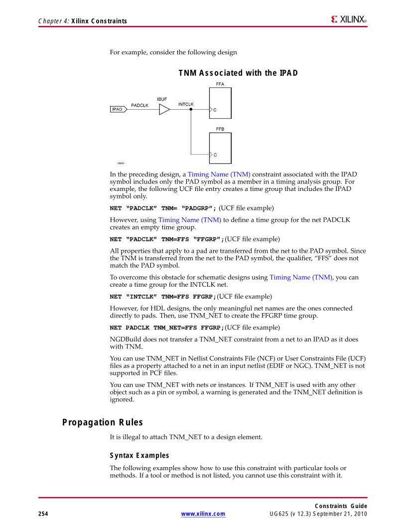
Chapter 4: Xilinx Constraints
For example, consider the following design
TNM Associated with the IPAD
In the preceding design, a Timing Name (TNM) constraint associated with the IPADsymbol includes only the PAD symbol as a member in a timing analysis group. Forexample, the following UCF file entry creates a time group that includes the IPADsymbol only.
NET “PADCLK” TNM= “PADGRP”; (UCF file example)
However, using Timing Name (TNM) to define a time group for the net PADCLKcreates an empty time group.
NET “PADCLK” TNM=FFS “FFGRP”;(UCF file example)
All properties that apply to a pad are transferred from the net to the PAD symbol. Sincethe TNM is transferred from the net to the PAD symbol, the qualifier, “FFS” does notmatch the PAD symbol.
To overcome this obstacle for schematic designs using Timing Name (TNM), you cancreate a time group for the INTCLK net.
NET “INTCLK” TNM=FFS FFGRP;(UCF file example)
However, for HDL designs, the only meaningful net names are the ones connecteddirectly to pads. Then, use TNM_NET to create the FFGRP time group.
NET PADCLK TNM_NET=FFS FFGRP;(UCF file example)
NGDBuild does not transfer a TNM_NET constraint from a net to an IPAD as it doeswith TNM.
You can use TNM_NET in Netlist Constraints File (NCF) or User Constraints File (UCF)files as a property attached to a net in an input netlist (EDIF or NGC). TNM_NET is notsupported in PCF files.
You can use TNM_NET with nets or instances. If TNM_NET is used with any otherobject such as a pin or symbol, a warning is generated and the TNM_NET definition isignored.
Propagation RulesIt is illegal to attach TNM_NET to a design element.
Syntax ExamplesThe following examples show how to use this constraint with particular tools ormethods. If a tool or method is not listed, you cannot use this constraint with it.
Constraints Guide254 www.xilinx.com UG625 (v 12.3) September 21, 2010

Chapter 4: Xilinx Constraints
Schematic Syntax• Attach to a net• Attribute Name
TNM_NET
• Attribute Values identifierFor a list of the constraint values, see the UCF and NCF Syntax section below.
UCF and NCF Syntax{NET|INST} “net_name” TNM_NET=[predefined_group:]identifier;• predefined_group can be:
– All of the members of a predefined group using the following keywords:♦ FF
♦ LATCH
♦ PAD
♦ RAM
♦ HSIOS
♦ DSP
♦ BRAM_PORTA
♦ BRAM_PORTB
♦ MULT
♦ FFS refers to all CLB and IOB flip-flops. Flip-flops built from functiongenerators are not included.
♦ RAMS refers to all RAMs for architectures with RAMS. This includes LUTRAMS and BLOCK RAMS.
♦ PADS refers to all I/O pads.♦ MULTS group the Spartan®-3, Spartan-3A, and Spartan-3E registered
multiplier.♦ DSPS is used to group DSP elements like the Virtex-4 DSP48.♦ LATCHES refers to all CLB or IOB latches. Latches built from function
generators are not included.– A subset of elements in a predefined_group can be defined as follows:
predefined_group (name_qualifier1... name_qualifiern)wherename_qualifiern can be any combination of letters, numbers, or underscores. Thename_qualifier type (net or instance) is based on the element type that TNM_NETis placed on. If the TNM_NET is on a NET, the name_qualifier is a net name. Ifthe TNM_NET is an instance (INST), the name_qualifier is an instance name.ExampleNET clk TNM_NET = FFS (my_flop) Grp1;
INST clk TNM_NET = FFS (my_macro) Grp2;
• identifier can be any combination of letters, numbers, or underscores.
The identifier cannot be any the following reserved words: FFS, RAMS, LATCHES,PADS, CPUS, HSIOS, MULTS, RISING, FALLING, TRANSHI, TRANSLO, or EXCEPT.
In addition, do not use the reserved words shown in the TNM (Timing Name) constraintReserved Words table as identifier.
Constraints GuideUG625 (v 12.3) September 21, 2010 www.xilinx.com 255
Chapter 4: Xilinx Constraints
The following statement identifies all flip-flops fanning out from the PADCLK net as amember of the timing group GRP1.
NET “PADCLK” TNM_NET=FFS ”GRP1”;
XCF SyntaxXST supports TNM_NET with the following limitation: only a single pattern supportedfor predefined groups.
The following command syntax is supported:
NET “PADCLK” TNM_NET=FFS ”GRP1”;
The following command syntax is not supported:
NET “PADCLK” TNM_NET = FFS(machine/*:xcounter/*) TG1;
Constraints Editor SyntaxFor information on setting constraints in Constraints Editor, including syntax, see theConstraints Editor Help.
PlanAhead™ SyntaxFor more information about using the PlanAhead™ software to create constraints, seeFloorplanning the Design in the PlanAhead User Guide. See PlanAhead in this Guide forinformation about:
• Defining placement constraints
• Assigning placement constraints
• Defining I/O pin configurations
• Floorplanning and placement constraints
TPSYNC (Timing Point Synchronization)The TPSYNC (Timing Point Synchronization) constraint:
• Is a grouping constraint.
• Flags a particular point or a set of points with an identifier for use in subsequenttiming specifications. If you use the same identifier on several points, timinganalysis treats the points as a group
Architecture SupportApplies to FPGA devices. Does not apply to CPLD devices.
Applicable Elements• Nets
• Instances
• Pins
Constraints Guide256 www.xilinx.com UG625 (v 12.3) September 21, 2010
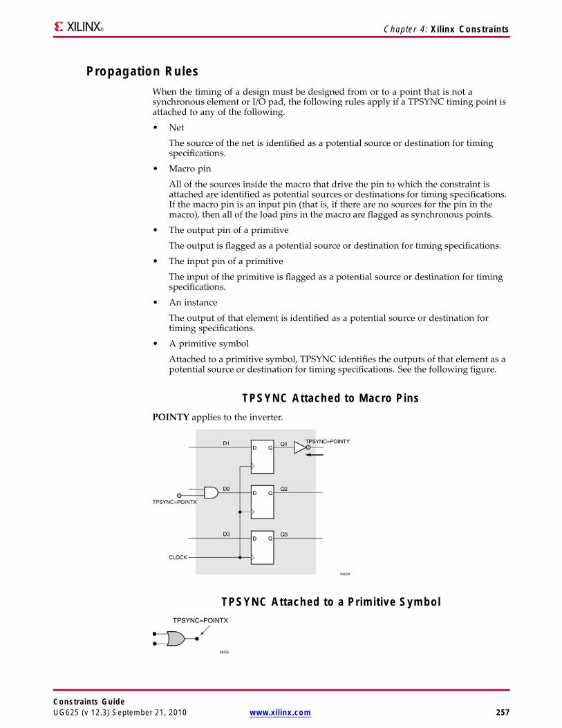
Chapter 4: Xilinx Constraints
Propagation RulesWhen the timing of a design must be designed from or to a point that is not asynchronous element or I/O pad, the following rules apply if a TPSYNC timing point isattached to any of the following.
• Net
The source of the net is identified as a potential source or destination for timingspecifications.
• Macro pin
All of the sources inside the macro that drive the pin to which the constraint isattached are identified as potential sources or destinations for timing specifications.If the macro pin is an input pin (that is, if there are no sources for the pin in themacro), then all of the load pins in the macro are flagged as synchronous points.
• The output pin of a primitive
The output is flagged as a potential source or destination for timing specifications.
• The input pin of a primitive
The input of the primitive is flagged as a potential source or destination for timingspecifications.
• An instance
The output of that element is identified as a potential source or destination fortiming specifications.
• A primitive symbol
Attached to a primitive symbol, TPSYNC identifies the outputs of that element as apotential source or destination for timing specifications. See the following figure.
TPSYNC Attached to Macro PinsPOINTY applies to the inverter.
TPSYNC Attached to a Primitive Symbol
Constraints GuideUG625 (v 12.3) September 21, 2010 www.xilinx.com 257

Chapter 4: Xilinx Constraints
Working with Two GatesUsing a TPSYNC timing point to define a synchronous point in a design implies thatthe flagged point cannot be merged into a function generator. For example, in thefollowing diagram, because of the TPSYNC definition, the two gates cannot be mergedinto a single function generator.
Syntax ExamplesThe following examples show how to use this constraint with particular tools ormethods. If a tool or method is not listed, you cannot use this constraint with it.
ValuesThis constraint has the following values:
identifier is a name that is used in timing specifications in the same way that groupsare used
Schematic Syntax• Attached to a net, instance, or pin
• Attribute Name
TPSYNC
• Attribute Values
See Values section above.
UCF and NCF SyntaxNET “net_name” TPSYNC=identifier;
INST “instance_name” TPSYNC=identifier;
PIN “pin_name” TPSYNC=identifier;
All flagged points are used as a source or destination or both for the specification wherethe TPSYNC identifier is used.
The name for the identifier must be unique to any identifier used for a TNM orTNM_NET grouping constraint.
The following statement identifies latch as a potential source or destination for timingspecifications for the net logic_latch.
NET “logic_latch” TPSYNC=latch;
Constraints Editor SyntaxFor information on setting constraints in Constraints Editor, including syntax, see theConstraints Editor Help.
Constraints Guide258 www.xilinx.com UG625 (v 12.3) September 21, 2010

Chapter 4: Xilinx Constraints
TPTHRU (Timing Thru Points)The TPTHRU (Timing Thru Points) constraint:• Is a grouping constraint.• Flags a particular point or set of points with an identifier for reference in subsequent
timing specifications.
Note If you use the same identifier on several points, timing analysis treats thepoints as a group. For more information, see TIMESPEC (Timing Specifications).
• Defines intermediates points on a path to which a specification applies.For more information, see TSidentifier (Timing Specification Identifier).
Architecture SupportApplies to FPGA devices. Does not apply to CPLD devices.
Applicable Elements• Nets• Pins• Instances
Propagation RulesNot applicable
Syntax ExamplesThe following examples show how to use this constraint with particular tools ormethods. If a tool or method is not listed, you cannot use this constraint with it.
Schematic Syntax• Attach to a net, instance, or pin• Attribute Name
TPTHRU
• Attribute Valuesidentifier
For more information, see UCF and NCF Syntax below.
UCF and NCF SyntaxNET “net_name” TPTHRU=identifier;
INST “instance_name” TPTHRU=identifier;
PIN “instance_name.pin_name” TPTHRU=”thru_group_name”;
whereidentifier is used in timing specifications to further qualify timing paths within a design.
The identifier name must be different from any identifier used for a TNM constraint.
Constraints GuideUG625 (v 12.3) September 21, 2010 www.xilinx.com 259
Chapter 4: Xilinx Constraints
Using TPTHRU in a FROM TO ConstraintIt is sometimes convenient to define intermediate points on a path to which aspecification applies. This defines the maximum allowable delay and has the syntaxshown in the following sections.
UCF Syntax with TIMESPECTIMESPEC “TSidentifier”=FROM “source_group” THRU “thru_point” [THRU“thru_point”] TO “dest_group” allowable_delay [units];
TIMESPEC “TSidentifier”=FROM “source_group” THRU “thru_point” [THRU“thru_point”] allowable_delay [units];
where
• identifier is an ASCII string made up of the characters A..Z, a..z, 0..9, and underscore(_)
• source_group and dest_group are user-defined groups, predefined groups or TPSYNCs
• thru_point is an intermediate point used to qualify the path, defined using aTPTHRU constraint
• allowable_delay is the timing requirement
• units is an optional field to indicate the units for the allowable delay. Default unitsare nanoseconds, but the timing number can be followed by ps, ns, micro, ms, GHz,MHz, or KHz to indicate the intended units.
The example shows how to use the TPTHRU constraint with the THRU constraint on aschematic. The UCF syntax is as follows.
INST “FLOPA” TNM=”A”;
INST “FLOPB” TNM=”B”;
NET “MYNET” TPTHRU=”ABC”;
TIMESPEC “TSpath1”=FROM “A” THRU “ABC” TO “B” 30;
The following statement identifies the net on_the_way as an intermediate point on apath to which the timing specification named “here” applies.
NET “on_the_way” TPTHRU=”here”;
Note The following NCF construct is not supported.
TIMESPECT “TS_1”=THRU “Thru_grp” 30.0
Constraints Editor SyntaxFor information on setting constraints in Constraints Editor, including syntax, see theConstraints Editor Help.
PCF SyntaxPATH "name"=FROM "source" THRU "thru_pt1" THRU "thru_ptn" TO "destination";
Constraints Guide260 www.xilinx.com UG625 (v 12.3) September 21, 2010

Chapter 4: Xilinx Constraints
You are not required to have a FROM, THRU, and TO. You can have almost anycombination, such as:
• FROM-TO
• FROM-THRU-TO
• THRU-TO
• TO
• FROM
• FROM-THRU-THRU-THRU-TO
• FROM-THRU
There is no restriction on the number of THRU points. The source, THRU points, anddestination can be a net, bel, comp, macro, pin, or timegroup.
TSidentifier (Timing Specification Identifier)TSidentifier (Timing Specification Identifier) is a basic timing constraint. TSidentifierproperties beginning with the letters TS are used with the TIMESPEC in a UserConstraints File (UCF). The value of TSidentifier corresponds to a specific timingspecification that can then be applied to paths in the design.
Architecture SupportApplies to all FPGA devices and all CPLD devices.
Applicable ElementsTIMESPEC keywords
Propagation RulesIt is illegal to attach TSidentifier to a net, signal, or design element.
Syntax ExamplesThe following examples show how to use this constraint with particular tools ormethods. If a tool or method is not listed, you cannot use this constraint with it.
All the following syntax definitions use a space as a separator. The use of a colon asa separator is optional.
UCF and NCF SyntaxDefining a Maximum Allowable Delay
TIMESPEC “TSidentifier”=FROM “source_group” TO “dest_group” allowable_delay [units];
Defining Intermediate Points (UCF)
TIMESPEC “TSidentifier”=FROM “source_group” THRU “thru_point” [THRU“thru_point1”... “thru_pointn”] TO “dest_group” allowable_delay [units];
Constraints GuideUG625 (v 12.3) September 21, 2010 www.xilinx.com 261

Chapter 4: Xilinx Constraints
where
• identifier is an ASCII string made up of the characters A-Z, a-z, 0-9, and _
• source_group and dest_group are user-defined or predefined groups
• thru_point is an intermediate point used to qualify the path, defined using aTPTHRU constraint
• allowable_delay is the timing requirement value
• units is an optional field to indicate the units for the allowable delay. The defaultunits are nanoseconds (ns), but the timing number can be followed by ps, ns, micro,ms, GHz, MHz, or kHz to indicate the intended units.
Defining a Linked Specification
This allows you to link the timing number used in one specification to anotherspecification.
TIMESPEC “TSidentifier”=FROM “source_group” TO “dest_group” another_TSid [/ |*] number;
where
• identifier is an ASCII string made up of the characters A-Z, a-z, 0-9, and _
• source_group and dest_group are user-defined or predefined groups
• another_Tsid is the name of another timespec
• number is a floating point number
Defining a Clock Period
This allows more complex derivative relationships to be defined as well as a simpleclock period.
TIMESPEC “TSidentifier”=PERIOD “TNM_reference” value [units] [{HIGH | LOW}[high_or_low_time [hi_lo_units]]] INPUT_JITTER value;
where
• identifier is a reference identifier with a unique name
• TNM_reference is the identifier name attached to a clock net (or a net in the clockpath) using a TNM constraint
• value is the required clock period
• units is an optional field to indicate the units for the allowable delay. The defaultunits are nanoseconds (ns), but the timing number can be followed by micro, ms, ps,ns, GHz, MHz, or kHz to indicate the intended units
• HIGH or LOW can be optionally specified to indicate whether the first pulse isto be High or Low
• high_or_low_time is the optional High or Low time, depending on the precedingkeyword. If an actual time is specified, it must be less than the period. If no High orLow time is specified, the default duty cycle is 50 percent.
• hi_lo_units is an optional field to indicate the units for the duty cycle. The default isnanoseconds (ns), but the High or Low time number can be followed by ps, micro,ms, ns or % if the High or Low time is an actual time measurement.
Specifying Derived Clocks
TIMESPEC “TSidentifier”=PERIOD “TNM_reference” “another_PERIOD_identifier” [/ | *]number [{HIGH | LOW} [high_or_low_time [hi_lo_units]]] INPUT_JITTER value;
Constraints Guide262 www.xilinx.com UG625 (v 12.3) September 21, 2010

Chapter 4: Xilinx Constraints
where• TNM_reference is the identifier name attached to a clock net (or a net in the clock
path) using a TNM constraint• another_PERIOD_identifier is the name of the identifier used on another period
specification• number is a floating point number• HIGH or LOW can be optionally specified to indicate whether the first pulse is
to be High or Low• high_or_low_time is the optional High or Low time, depending on the preceding
keyword. If an actual time is specified, it must be less than the period. If no High orLow time is specified, the default duty cycle is 50 percent.
• hi_lo_units is an optional field to indicate the units for the duty cycle. The default isnanoseconds (ns), but the High or Low time number can be followed by ps, micro,ms, or % if the High or Low time is an actual time measurement.
Ignoring Paths
Note This form is not supported for CPLD devices.
There are situations in which a path that exercises a certain net should be ignoredbecause all paths through the net, instance, or instance pin are not important from atiming specification point of view.
TIMESPEC “TSidentifier”=FROM “source_group” TO “dest_group” TIG;
or
TIMESPEC “TSidentifier”=FROM “source_group” THRU “thru_point” [THRU“thru_point1”... “thru_pointn”] TO “dest_group” TIG;
where• identifier is an ASCII string made up of the characters A-Z, a-z 0-9, and _• source_group and dest_group are user-defined or predefined groups• thru_point is an intermediate point used to qualify the path, defined using a
TPTHRU constraint
The following statement says that the timing specification TS_35 calls for a maximumallowable delay of 50 ns between the groups here and there.
TIMESPEC “TS_35”=FROM “here” TO “there” 50;
The following statement says that the timing specification TS_70 calls for a 25 ns clockperiod for clock_a, with the first pulse being High for a duration of 15 ns.
TIMESPEC “TS_70”=PERIOD “clock_a” 25 high 15;
For more information, see Logical Constraints and Physical Constraints in Chapter 2,“Constraint Types.”
Constraints Editor SyntaxFor information on setting constraints in Constraints Editor, including syntax, see theConstraints Editor Help.
Clock period constraints are entered using the Clock Domains entry. Input setup timeis entered using the Inputs entry. Clock-to-output delay is entered using the Outputsentry. Pad-to-pad delays are entered using the Exceptions > Paths category.
PCF SyntaxThe same as the UCF syntax without the TIMESPEC keyword.
Constraints GuideUG625 (v 12.3) September 21, 2010 www.xilinx.com 263

Chapter 4: Xilinx Constraints
FPGA Editor SyntaxFor information on setting constraints in FPGA Editor, including syntax, see the FPGAEditor Help.
U_SET (U SET)The U_SET (U SET) constraint:• Is an advanced mapping constraint.• Groups design elements with attached RLOC constraints that are distributed
throughout the design hierarchy into a single set.The elements that are members of a U_SET can cross the design hierarchy. You canarbitrarily select objects without regard to the design hierarchy and tag them asmembers of a U_SET. For more information, see RLOC Sets.
Architecture SupportApplies to FPGA devices. Does not apply to CPLD devices.
Applicable ElementsThis constraint may be used with an FPGA device in one or more of the following designelements, or categories of design elements. Not all devices support all elements. To seewhich design elements can be used with which devices, see the Libraries Guides. Formore information, see the device data sheet.
• Registers• Macro Instance• FMAP
• ROM
• RAMS
• RAMD
• BUFT
• MULT18X18S
• RAMB4_Sm_Sn
• RAMB4_Sn
• RAMB16_Sm_Sn
• RAMB16_Sn
• RAMB16
• DSP48
Propagation RulesThis constraint is a macro constraint. Any attachment to a net is illegal.
Syntax ExamplesThe following examples show how to use this constraint with particular tools ormethods. If a tool or method is not listed, you cannot use this constraint with it.
Constraints Guide264 www.xilinx.com UG625 (v 12.3) September 21, 2010

Chapter 4: Xilinx Constraints
Schematic Syntax• Attach to a valid instance
• Attribute Name: U_SET
• Attribute Values: name
where
name is the identifier of the set
VHDL SyntaxDeclare the VHDL constraint as follows:
attribute U_SET: string;
Specify the VHDL constraint as follows:
attribute U_SET of {component_name |label_name}: {component|label} isname;
where
name is the identifier of the set
For more information about basic VHDL syntax, see VHDL Attributes.
Verilog SyntaxPlace the Verilog constraint immediately before the module or instantiation.
Specify the Verilog constraint as follows:
(* U_SET = name *)
where
name is the identifier of the set
For more information about basic Verilog syntax, see Verilog Attributes.
UCF and NCF SyntaxINST "instance_name" U_SET= name;
where
name is the identifier of the set
This name is absolute. It is not prefixed by a hierarchical qualifier.
The following statement specifies that the design element ELEM_1 be in a set calledJET_SET.
INST "$1I3245/ELEM_1" U_SET=JET_SET;
XCF SyntaxBEGIN MODEL entity_name
INST "instance_name" U_SET=uset_name;
END;
Constraints GuideUG625 (v 12.3) September 21, 2010 www.xilinx.com 265

Chapter 4: Xilinx Constraints
Use Internal VREF (USE_INTERNAL_VREF)The Use Internal Vref (USE_INTERNAL_VREF) constraint:• Provides a means of assigning a voltage value to the internal Vref feature for a
given IO bank.• Frees the Vref pins of IO banks from their function of providing a voltage reference.• Allows you to specify the Vref pins for either Vref or an alternative use.
Architecture SupportApplies to Virtex®-6 devices only.
Applicable ElementsThis constraint can be specified for an instance, comp or net.
Propagation RulesUSE_INTERNAL_VREF is illegal when attached to a net except when the net isconnected to a pad. In this case, USE_INTERNAL_VREF is treated as attached to thepad instance. When attached to a design element, USE_INTERNAL_VREF applies tothe entity to which it is attached.
Syntax ExamplesThe following examples show how to use this constraint with particular tools ormethods. If a tool or method is not listed, you cannot use this constraint with it.
ValuesThis constraint has the following values:• TRUE
Turns on the constraint for a specific element• FALSE
Turns off the constraint for a specific element• DONT_CARE
Allows the tools to determine the use of the Vref pin
Schematic Syntax• Attribute Name
USE_INTERNAL_VREF• Attribute Values
See Values section above.
Verilog SyntaxPlace the Verilog constraint immediately before the module or instantiation.
Specify the Verilog constraint as follows:
(* USE_INTERNAL_VREF = “{TRUE|FALSE|DONT_CARE}” *)
The default is DONT_CARE.
For more information about basic Verilog syntax, see Verilog Attributes.
Constraints Guide266 www.xilinx.com UG625 (v 12.3) September 21, 2010

Chapter 4: Xilinx Constraints
UCF and NCF SyntaxINST “instance_name” USE_INTERNAL_VREF={TRUE|FALSE|DONT_CARE};
The default is TRUE.
XCF SyntaxMODEL “entity_name” use_internal_vref ={true|false|dont_care}
The default is TRUE.
USE_LUTNM (Use LUTNM)The USE_LUTNM (Use LUTNM) constraint:• Is an advanced mapping and placement constraint.• Turns LUTNM (Lookup Table Name) on or off for a specific element or section
of a set.
Architecture SupportApplies to FPGA devices. Does not apply to CPLD devices.
Applicable ElementsApplies to instances or macros that are members of sets.
Propagation RulesIt is illegal to attach USE_LUTNM to a net.
Syntax ExamplesThe following examples show how to use this constraint with particular tools ormethods. If a tool or method is not listed, you cannot use this constraint with it.
ValuesThis constraint has the following values:
• TRUETurns on the constraint for a specific element
• FALSETurns off the constraint for a specific element
The default is TRUE.
Schematic Syntax• Attach to a member of a set• Attribute Name
USE_LUTNM• Attribute Values
See Values section above.
VHDL SyntaxDeclare the VHDL constraint as follows:
Constraints GuideUG625 (v 12.3) September 21, 2010 www.xilinx.com 267

Chapter 4: Xilinx Constraints
attribute USE_LUTNM: string;
Specify the VHDL constraint as follows:
attribute USE_LUTNM of entity_name: entity is “{TRUE|FALSE}”;
For more information about basic VHDL syntax, see VHDL Attributes.
Verilog SyntaxPlace the Verilog constraint immediately before the module or instantiation.
Specify the Verilog constraint as follows:
(* USE_LUTNM = “{TRUE|FALSE}” *)
For more information about basic Verilog syntax, see Verilog Attributes.
UCF and NCF SyntaxINST “instance_name” USE_LUTNM={TRUE|FALSE};
XCF SyntaxMODEL “entity_name” use_lutnm={true|false};
USE_RLOC (Use Relative Location)The USE_RLOC (Use Relative Location) constraint:
• Is an advanced mapping and placement constraint.
• Turns RLOC on or off for a specific element or section of a set.
Architecture SupportApplies to FPGA devices. Does not apply to CPLD devices.
Applicable ElementsApplies to instances or macros that are members of sets.
Propagation RulesIt is illegal to attach USE_RLOC to a net. When attached to a design element, U_SETpropagates to all applicable elements in the hierarchy within the design element.
Constraints Guide268 www.xilinx.com UG625 (v 12.3) September 21, 2010

Chapter 4: Xilinx Constraints
Using the USE_RLOC Constraint to Control RLOC Application onH_SET and HU_SET Sets
Applying USE_RLOC on U_SET sets is a special case because of the lack of hierarchyin the U_SET set. Because USE_RLOC propagates strictly in a hierarchical manner, themembers of a U_SET set that are in different parts of the design hierarchy must betagged separately with USE_RLOC. No single USE_RLOC constraint is propagated toall the members of the set that lie in different parts of the hierarchy.
If you create a U_SET set through an instantiating macro, you can attach USE_RLOCto the instantiating macro to allow it to propagate hierarchically to all the membersof the set.
You can create this instantiating macro by placing U_SET on a macro and letting themapper propagate that constraint to every symbol with an RLOC constraint belowit in the hierarchy.
Constraints GuideUG625 (v 12.3) September 21, 2010 www.xilinx.com 269
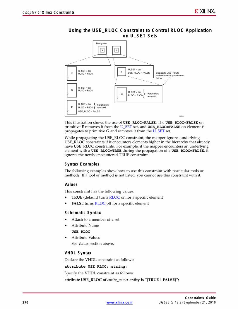
Chapter 4: Xilinx Constraints
Using the USE_RLOC Constraint to Control RLOC Applicationon U_SET Sets
This illustration shows the use of USE_RLOC=FALSE. The USE_RLOC=FALSE onprimitive E removes it from the U_SET set, and USE_RLOC=FALSE on element Fpropagates to primitive G and removes it from the U_SET set.
While propagating the USE_RLOC constraint, the mapper ignores underlyingUSE_RLOC constraints if it encounters elements higher in the hierarchy that alreadyhave USE_RLOC constraints. For example, if the mapper encounters an underlyingelement with a USE_RLOC=TRUE during the propagation of a USE_RLOC=FALSE, itignores the newly encountered TRUE constraint.
Syntax ExamplesThe following examples show how to use this constraint with particular tools ormethods. If a tool or method is not listed, you cannot use this constraint with it.
ValuesThis constraint has the following values:• TRUE (default) turns RLOC on for a specific element• FALSE turns RLOC off for a specific element
Schematic Syntax• Attach to a member of a set• Attribute Name
USE_RLOC
• Attribute ValuesSee Values section above.
VHDL SyntaxDeclare the VHDL constraint as follows:
attribute USE_RLOC: string;
Specify the VHDL constraint as follows:
attribute USE_RLOC of entity_name: entity is “{TRUE | FALSE}”;
Constraints Guide270 www.xilinx.com UG625 (v 12.3) September 21, 2010

Chapter 4: Xilinx Constraints
For more information about basic VHDL syntax, see VHDL Attributes.
Verilog SyntaxPlace the Verilog constraint immediately before the module or instantiation.
Specify the Verilog constraint as follows:
(* USE_RLOC = “{TRUE|FALSE}” *)
For more information about basic Verilog syntax, see Verilog Attributes.
UCF and NCF SyntaxINST “instance_name” USE_RLOC={TRUE | FALSE};
XCF SyntaxMODEL “entity_name” use_rloc={true | false};
Use Low Skew Lines (USELOWSKEWLINES)The Use Low Skew Lines (USELOWSKEWLINES) constraint:• Is a PAR routing constraint.• Specifies the use of low skew routing resources for any net. You can use these
resources for both internally generated and externally generated signals.Externally generated signals are those driven by IOBs. USELOWSKEWLINES on a netdirects PAR to route the net on one of the low skew resources. When this constraint isused, the timing tool automatically accounts for and reports skew on register-to-registerpaths that utilize those low skew resources. Specify USELOWSKEWLINES only whenall four primary global clocks have been used.
Architecture SupportApplies to Virtex®-4 devices and higher and to Spartan®-3 devices and higher.
Applicable ElementsNets
Propagation RulesApplies to attached net
Syntax ExamplesThe following examples show how to use this constraint with particular tools ormethods. If a tool or method is not listed, you cannot use this constraint with it.
ValuesThis constraint has the following values:• YES• NO• TRUE• FALSE
Constraints GuideUG625 (v 12.3) September 21, 2010 www.xilinx.com 271

Chapter 4: Xilinx Constraints
Schematic Syntax• Attach to an output net• Attribute Name
USELOWSKEWLINES• Attribute Values
– TRUE– FALSE
VHDL SyntaxDeclare the VHDL constraint as follows:
attribute USELOWSKEWLINES: string;
Specify the VHDL constraint as follows:
attribute USELOWSKEWLINES of signal_name: signal is “{YES|NO|TRUE|FALSE}”;
For more information about basic VHDL syntax, see VHDL Attributes.
Verilog SyntaxPlace the Verilog constraint immediately before the module or instantiation.
Specify the Verilog constraint as follows:
(* USELOWSKEWLINES = “{YES|NO|TRUE|FALSE}” *)
For more information about basic Verilog syntax, see Verilog Attributes.
UCF and NCF SyntaxThis statement forces net $1I87/1N6745 to be routed on one of the device’s low skewresources.
NET “$1I87/$1N6745” USELOWSKEWLINES;
XCF SyntaxBEGIN MODEL “entity_name”
NET “signal_name” uselowskewlines={yes|true};
END;
Constraints Editor SyntaxFor information on setting constraints in Constraints Editor, including syntax, see theConstraints Editor Help.
PCF SyntaxSame as UCF and NCF Syntax above.
VCCAUX (VCCAUX)The VCCAUX (VCCAUX) constraint:• Defines the voltage value of the VCCAUX pin for a Spartan®-3A device.• Affects the banking rules for I/O placement within the automated placer, as well as
in the PACE pin assignments software.• Affects the end-generated bitstream for the device.
Constraints Guide272 www.xilinx.com UG625 (v 12.3) September 21, 2010

Chapter 4: Xilinx Constraints
Architecture SupportApplies to Spartan®-3A devices only.
Applicable ElementsVCCAUX is a global attribute for the Spartan-3A device and is not attached to anyparticular element.
Syntax ExamplesThe following examples show how to use this constraint with particular tools ormethods. If a tool or method is not listed, you cannot use this constraint with it.
ValuesThis constraint has the following values:• 2.5• 3.3
UCF and NCF SyntaxCONFIG VCCAUX="value";
Example
CONFIG VCCAUX=3.3;
VOLTAGE (Voltage)The VOLTAGE (Voltage) constraint:• Is a timing constraint.• Allows the specification of the operating voltage, which provides a means of
prorating delay characteristics based on the specified voltage.Prorating is a scaling operation on existing speed file delays and is applied globallyto all delays.
Note Newer devices may not support VOLTAGE prorating until the timing information(speed files) are marked as production status.
Each architecture has its own specific range of supported voltages. If the enteredvoltage does not fall within the supported range, the constraint is ignored and anarchitecture-specific default value is used instead. The error message for this conditionappears during static timing.
Architecture SupportThe following FPGA devices are supported for VOLTAGE:• Spartan®-3A• Spartan-3E• Virtex®-4• Virtex-5
Applicable ElementsApplies globally to the entire design.
Constraints GuideUG625 (v 12.3) September 21, 2010 www.xilinx.com 273

Chapter 4: Xilinx Constraints
Propagation RulesIt is illegal to attach this constraint to a net, signal, or design element.
Syntax ExamplesThe following examples show how to use this constraint with particular tools ormethods. If a tool or method is not listed, you cannot use this constraint with it.
UCF and NCF SyntaxVOLTAGE=value [V];
where• value is a real number specifying the voltage• V indicates volts, the default voltage unit
The following statement specifies that the analysis for everything relating to speed filedelays assumes an operating power of 5 volts.
VOLTAGE=5;
Constraints Editor SyntaxFor information on setting constraints in Constraints Editor, including syntax, see theConstraints Editor Help.
PCF SyntaxSame as UCF Syntax.
VREF (VREF)The VREF (VREF) constraint:• Applies to the design as a global attribute (not directly applicable to any element
in the design).• Configures listed pins as VREF supply pins to be used in conjunction with other I/O
pins designated with one of the SSTL or HSTL I/O Standards.
Because VREF is selectable on any I/O in CoolRunner™-II designs, it allows you to selectwhich pins are VREF pins. Double-check pin assignment in the report (RPT) file. If youdo not specify any VREF pins for the differential I/O standards, HSTL and SSTL, or ifyou do not specify sufficient VREF pins within the required proximity of differentialI/O pins, the fitter automatically assigns sufficient VREF.
Architecture SupportApplies only to CoolRunner-II devices with 128 macrocells and larger.
Applicable ElementsApplies globally to the entire design.
Propagation RulesConfigures listed pins as VREF supply pins to be used in conjunction with other I/O pinsdesignated with one of the SSTL or HSTL I/O Standards.
Constraints Guide274 www.xilinx.com UG625 (v 12.3) September 21, 2010

Chapter 4: Xilinx Constraints
Syntax ExamplesThe following examples show how to use this constraint with particular tools ormethods. If a tool or method is not listed, you cannot use this constraint with it.
ValuesThis constraint has the following values:
• Pnn
where
nn is a numeric pin number
• rc
where
– r=alphabetic row
– c=numeric column
Schematic SyntaxVREF=value_list (on CONFIG symbol)
UCF and NCF SyntaxCONFIG VREF=value_list;
CONFIG VREF=P12,P13;
WIREAND (Wire And)The WIREAND (Wire And) constraint:
• Is an advanced fitter constraint
• Forces a tagged node to be implemented as a wired AND function in the interconnect(UIM and Fastconnect)
Architecture SupportApplies to XC9500 devices only.
Applicable ElementsAny net
Propagation RulesThis constraint is a net constraint. Any attachment to a design element is illegal.
Syntax ExamplesThe following examples show how to use this constraint with particular tools ormethods. If a tool or method is not listed, you cannot use this constraint with it.
Constraints GuideUG625 (v 12.3) September 21, 2010 www.xilinx.com 275

Chapter 4: Xilinx Constraints
Schematic Syntax• Attach to a net• Attribute Name
WIREAND
• Attribute Values– TRUE
– FALSE
VHDL SyntaxDeclare the VHDL constraint as follows:
attribute WIREAND: string;
Specify the VHDL constraint as follows:
attribute WIREAND of signal_name : signal is “{YES|NO|TRUE|FALSE}”;
For more information about basic VHDL syntax, see VHDL Attributes.
Verilog SyntaxPlace the Verilog constraint immediately before the module or instantiation.
Specify the Verilog constraint as follows:
(* WIREAND = “{YESE|NO|TRUE|FALSE}” *)
For more information about basic Verilog syntax, see Verilog Attributes.
UCF and NCF SyntaxThe following statement specifies that the net named SIG_11 be implemented asa wired AND when optimized.
NET “$I16789/SIG_11” WIREAND;
XBLKNM (XBLKNM)The XBLKNM (XBLKNM) constraint:• Is an advanced mapping constraint.• Assigns block names to qualifying primitives and logic elements.If the same XBLKNM attribute is assigned to more than one instance, the softwareattempts to pack logic with the same block name into one or more slices. Conversely, twosymbols with different XBLKNM names are not mapped into the same block. Placing thesame XBLKNM constraints on instances that do not fit within one block creates an error.
Specifying identical XBLKNM attributes on FMAP symbols tells the software to groupthe associated function generators into a single slice. Using XBLKNM, you can partitiona complete slice without constraining the slice to a physical location on the device.
Hierarchical paths are not prefixed to XBLKNM attributes, so XBLKNM attributes fordifferent slices must be unique throughout the entire design.
The BLKNM attribute allows any elements except those with a different BLKNM to bemapped into the same physical component. XBLKNM, however, allows only elementswith the same XBLKNM to be mapped into the same physical component. Elementswithout an XBLKNM cannot be not mapped into the same physical component as thosewith an XBLKNM.
XBLKNM can also be used with block RAMs.
Constraints Guide276 www.xilinx.com UG625 (v 12.3) September 21, 2010

Chapter 4: Xilinx Constraints
Architecture SupportApplies to FPGA devices. Does not apply to CPLD devices.
Applicable ElementsFor information about which design elements can be used with which device families,see the Libraries Guides. For more information, see the device data sheet.
Propagation RulesApplies to the design element to which it is attached.
Syntax ExamplesThe following examples show how to use this constraint with particular tools ormethods. If a tool or method is not listed, you cannot use this constraint with it.
ValuesThis constraint has the following values:block_name is a valid block name for that type of symbol
Schematic Syntax• Attach to a valid instance• Attribute Name
XBLKNM
• Attribute ValuesSee Values section above.
VHDL SyntaxDeclare the VHDL constraint as follows:
attribute XBLKNM: string;
Specify the VHDL constraint as follows:
attribute XBLKNM of {component_name|label_name}: {component|label} is block_name;
For more information about basic VHDL syntax, see VHDL Attributes.
Verilog SyntaxPlace the Verilog constraint immediately before the module or instantiation.
Specify the Verilog constraint as follows:
(* XBLKNM = "block_name" *)
For more information about basic Verilog syntax, see Verilog Attributes.
UCF and NCF SyntaxINST "instance_name" XBLKNM=block_name;
The following statement assigns an instantiation of an element named flip_flop2 toa block named U1358.
INST "$1I87/flip_flop2" XBLKNM=U1358;
Constraints GuideUG625 (v 12.3) September 21, 2010 www.xilinx.com 277
Chapter 4: Xilinx Constraints
XCF SyntaxBEGIN MODEL "entity_name"
INST "instance_name" xblknm=xblknm_name;
END;
Constraints Guide278 www.xilinx.com UG625 (v 12.3) September 21, 2010


![PHARMACOLOGY (12.3)]. - dailymed.nlm.nih.gov](https://static.fdocuments.us/doc/165x107/62955a8e9364f61d2d7d2fb3/pharmacology-123-.jpg)
