XC6223 Series · 1/37 XC6223 Series Built-in Inrush Current Protection, 300mA High Speed LDO...
37
1/37 XC6223 Series Built-in Inrush Current Protection, 300mA High Speed LDO Voltage Regulator ■APPLICATIONS ●Digital still cameras ●Smart phones / Mobile phones ●Portable game consoles ●Modules (wireless, cameras, etc. ) ●IC recorders ●Mobile devices / terminals ●Bluetooth ●Wireless LAN ●Digital TV tuners ■TYPICAL APPLICATION CIRCUIT ETR0339-009 ■FEATURES Maximum Output Current : 300mA Input Voltage Range : 1.6~5.5V Output Voltages : 2.0~4.0V (Accuracy ±1%) 1.2~1.95V (Accuracy ±20mV) 0.05V increments Dropout Voltage : 200mV@IOUT=300mA (VOUT=3.0V) Low Power Consumption : 100μA Stand-by Current : 0.1μA High Ripple Rejection : 80dB@f=1kHz Protection Circuits : Current Limit(400mA) Short Circuit Protection Over Heat Protection Inrush Current Protection Low ESR Capacitors : CIN =1.0μF, CL=1.0μF CE Function : Active High Operating Ambient Temperature CL High Speed Discharge -40℃~+105℃ Packages : USPQ-4B03 USP-4 SSOT-24 SOT-25 SOT-89-5 Environmentally Friendly : EU RoHS Compliant, Pb Free ■ TYPICAL PERFORMANCE CHARACTERISTICS ■GENERAL DESCRIPTION The XC6223 series is a high speed LDO regulator that features high accurate, low noise, high ripple rejection, low dropout and low power consumption. The series consists of a voltage reference, an error amplifier, a driver transistor, a current limiter, a phase compensation circuit, a thermal shutdown circuit and an inrush current protection circuit. The CE function enables the circuit to be in stand-by mode by inputting low level signal. In the stand-by mode, the series enables the electric charge at the output capacitor CL to be discharged via the internal switch, and as a result the VOUT pin quickly returns to the VSS level. The output stabilization capacitor CL is also compatible with low ESR ceramic capacitors. The output voltage is selectable in 0.05V increments within the range of 1.2V to 4.0V which fixed by laser trimming technologies. The over current protection circuit and the thermal shutdown circuit are built-in. These two protection circuits will operate when the output current reaches current limit level or the junction temperature reaches temperature limit level. tr = tf = 0.5μs, Ta = 25℃, I OUT = 1⇔150mA V IN = 3.5V, C IN = 1μF (ceramic), C L = 1μF (ceramic) XC6223x251 2.20 2.25 2.30 2.35 2.40 2.45 2.50 2.55 2.60 Time [20μs/div] Output Voltage: V OUT [V] 0 50 100 150 200 250 300 350 400 Output Current Iout[mA] Output Voltage Output Current
-
Upload
hoangthuan -
Category
Documents
-
view
229 -
download
0
Transcript of XC6223 Series · 1/37 XC6223 Series Built-in Inrush Current Protection, 300mA High Speed LDO...

1/37
XC6223 Series
Built-in Inrush Current Protection, 300mA High Speed LDO Voltage Regulator
APPLICATIONS Digital still cameras Smart phones / Mobile phones
Portable game consoles
Modules (wireless, cameras, etc. ) IC recorders Mobile devices / terminals
Bluetooth
Wireless LAN Digital TV tuners
TYPICAL APPLICATION CIRCUIT
ETR0339-009
FEATURESMaximum Output Current : 300mA Input Voltage Range : 1.6~5.5V Output Voltages : 2.0~4.0V (Accuracy ±1%) 1.2~1.95V (Accuracy ±20mV)
0.05V increments Dropout Voltage : 200mV@IOUT=300mA (VOUT=3.0V)Low Power Consumption : 100μA Stand-by Current : 0.1μA High Ripple Rejection : 80dB@f=1kHz Protection Circuits : Current Limit(400mA) Short Circuit Protection Over Heat Protection Inrush Current Protection Low ESR Capacitors : CIN =1.0μF, CL=1.0μF CE Function : Active High Operating Ambient Temperature
CL High Speed Discharge : -40~+105
Packages : USPQ-4B03 USP-4
SSOT-24 SOT-25 SOT-89-5 Environmentally Friendly : EU RoHS Compliant, Pb Free
TYPICAL PERFORMANCECHARACTERISTICS
GENERAL DESCRIPTION The XC6223 series is a high speed LDO regulator that features high accurate, low noise, high ripple rejection, low dropout
and low power consumption. The series consists of a voltage reference, an error amplifier, a driver transistor, a current limiter, a phase compensation circuit, a thermal shutdown circuit and an inrush current protection circuit.
The CE function enables the circuit to be in stand-by mode by inputting low level signal. In the stand-by mode, the series enables the electric charge at the output capacitor CL to be discharged via the internal switch, and as a result the VOUT pin quickly returns to the VSS level. The output stabilization capacitor CL is also compatible with low ESR ceramic capacitors.
The output voltage is selectable in 0.05V increments within the range of 1.2V to 4.0V which fixed by laser trimming technologies. The over current protection circuit and the thermal shutdown circuit are built-in. These two protection circuits will operate when the output current reaches current limit level or the junction temperature reaches temperature limit level.
tr = tf = 0.5μs, Ta = 25, IOUT = 1⇔150mA
VIN = 3.5V, CIN = 1μF (ceramic), CL = 1μF (ceramic)
XC6223x251
2.20
2.25
2.30
2.35
2.40
2.45
2.50
2.55
2.60
Time [20μs/div]
Outp
ut
Voltag
e: V
OU
T [
V]
0
50
100
150
200
250
300
350
400
Outp
ut
Curr
ent
Iout[
mA
]
Output Voltage
Output Current

2/37
XC6223 Series
PIN NUMBER PIN NAME FUNCTIONS
USPQ-4B03 USP-4 SSOT-24 SOT-25 SOT-89-5
4 4 4 1 4 VIN Power Input 1 1 3 5 5 VOUT Output 2 2 2 2 2 VSS Ground
3 3 1 3 3 CE ON/OFF Control - - - 4 1 NC No Connection
PIN NAME DESIGNATOR CONDITION
CE L 0V≦VCE≦0.3V H 1.0V≦VCE≦5.5V
OPEN CE=OPEN
PIN CONFIGURATION
PIN ASSIGNMENT
*The dissipation pad for the USPQ-4B03,USP-4 packages should be solder-plated in reference mount pattern and metal masking so as to enhance mounting strength and heat release. If the pad needs to be connected to other pins, it should be connected to the VSS (No. 2) pin.
LOGIC CONDITION FOR THE PIN

3/37
XC6223Series
DESIGNATOR ITEM SYMBOL DESCRIPTION
① Type of
Regulator
A/J(*3) Without Inrush Current Protection, Without CE Pull-down, Without CL discharge (Semi-Custom)B/K(*3) Without Inrush Current Protection, Without CE Pull-down, With CL discharge (Semi-Custom) C/M(*3) Without Inrush Current Protection, With CE Pull-down(*2), Without CL discharge (Semi-Custom)D/N(*3) Without Inrush Current Protection, With CE Pull-down(*2), With CL discharge E/P(*3) With Inrush Current Protection, Without CE Pull-down, Without CL discharge (Semi-Custom) F/Q(*3) With Inrush Current Protection, Without CE Pull-down, With CL discharge (Semi-Custom) G/R(*3) With Inrush Current Protection, With CE Pull-down(*2), Without CL discharge (Semi-Custom) H/T(*3) With Inrush Current Protection, With CE Pull-down(*2), With CL discharge
②③ Output Voltage 12~40 ex.) 2.80V → ②=2, ③=8, ④=please see down below.
④ Output Accuracy
1 ±1% (VOUT≧2.0V) ±0.02V (VOUT<2.0V) In case of 2nd decimal place 0 (ex.2.80V → ④=1)
B ±1% (VOUT≧2.0V) ±0.02V (VOUT<2.0V) In case of 2nd decimal place 5 (ex.2.85V → ④=B)
⑤⑥-⑦(*1) Packages
(Order Unit)
9R-G USPQ-4B03 (5,000/Reel) GR-G USP-4 (3,000/Reel) NR-G SSOT-24 (3,000/Reel) MR-G SOT-25 (3,000/Reel) PR-G SOT-89-5 (1,000/Reel)
CE LOGIC CONDITION
IC OPERATION
H Operation ON L Operation OFF(Stand-by)
OPEN *
PRODUCT CLASSIFICATIONOrdering Information
XC6223①②③④⑤⑥-⑦(*1)
(*1) The “-G” suffix denotes Halogen and Antimony free as well as being fully EU RoHS compliant. (*2) With CE pin pull-down resistor. (*3) Product types A/B/C/D/E/F/G/H are for pre-existing customers who were or are already using these types of products.
For customers who intend to adopt this product newly, please select from types J/K/M/N/P/Q/R/T which have been extended the operating temperature range (105compliance).
PIN FUNCTION ASSIGNMENT
* Undefined state in XC6223 A/B/E/F/J/K/P/Q. On the other hand, Operation OFF states in XC6223C/D/G/H/M/N/R/T because that an internal pull-down resister maintains the CE pin voltage to be low.

4/37
XC6223 Series
* Diodes inside the circuits are ESD protection diodes and parasitic diodes.
BLOCK DIAGRAMS
XC6223A/J series XC6223B/K series
XC6223C/M series XC6223D/N series
XC6223E/P series XC6223F/Q series
XC6223G/R series XC6223H/T series
5/37
XC6223Series
XC6223A/B/C/D/E/F/G/H Series
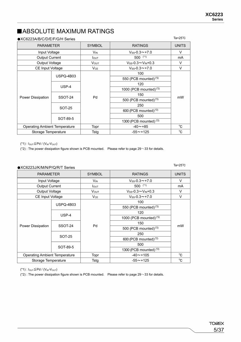
PARAMETER SYMBOL RATINGS UNITS
Input Voltage VIN VSS-0.3~+7.0 V Output Current IOUT 500 (*1) mA Output Voltage VOUT VSS-0.3~VIN+0.3 V
CE Input Voltage VCE VSS-0.3~+7.0 V
Power Dissipation
USPQ-4B03
Pd
100
mW
550 (PCB mounted) (*2)
USP-4 120
1000 (PCB mounted) (*2)
SSOT-24 150
500 (PCB mounted) (*2)
SOT-25 250
600 (PCB mounted) (*2)
SOT-89-5 500
1300 (PCB mounted) (*2) Operating Ambient Temperature Topr -40~+85
Storage Temperature Tstg -55~+125
XC6223J/K/M/N/P/Q/R/T Series
PARAMETER SYMBOL RATINGS UNITS
Input Voltage VIN VSS-0.3~+7.0 V Output Current IOUT 500 (*1) mA Output Voltage VOUT VSS-0.3~VIN+0.3 V
CE Input Voltage VCE VSS-0.3~+7.0 V
Power Dissipation
USPQ-4B03
Pd
100
mW
550 (PCB mounted) (*2)
USP-4 120
1000 (PCB mounted) (*2)
SSOT-24 150
500 (PCB mounted) (*2)
SOT-25 250
600 (PCB mounted) (*2)
SOT-89-5 500
1300 (PCB mounted) (*2) Operating Ambient Temperature Topr -40~+105
Storage Temperature Tstg -55~+125
ABSOLUTE MAXIMUM RATINGS
(*1) : IOUT≦Pd / (VIN-VOUT) (*2) : The power dissipation figure shown is PCB mounted. Please refer to page 29~33 for details.
(*1) : IOUT≦Pd / (VIN-VOUT) (*2) : The power dissipation figure shown is PCB mounted. Please refer to page 29~33 for details.
Ta=25
Ta=25
6/37
XC6223 Series
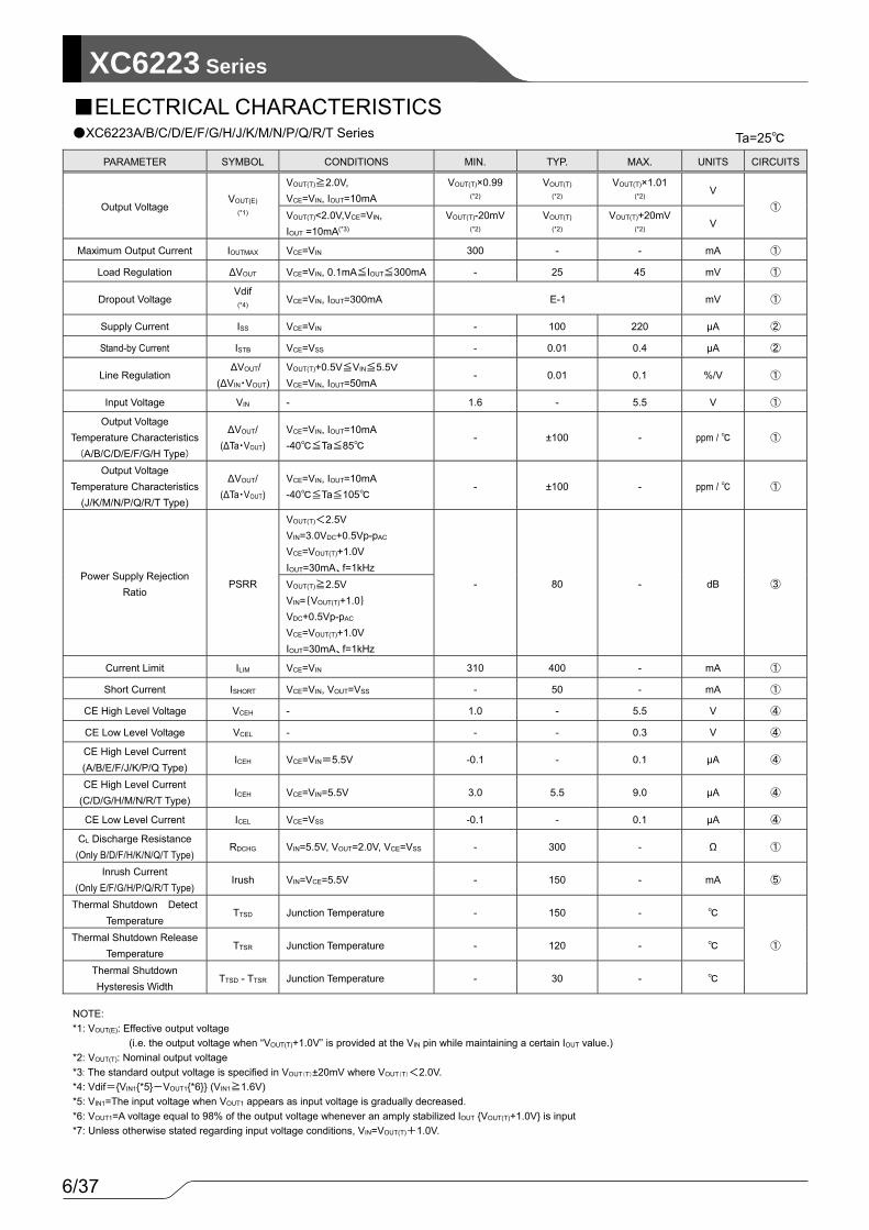
PARAMETER SYMBOL CONDITIONS MIN. TYP. MAX. UNITS CIRCUITS
Output Voltage VOUT(E)
(*1)
VOUT(T)≧2.0V, VCE=VIN, IOUT=10mA
VOUT(T)×0.99 (*2)
VOUT(T) (*2)
VOUT(T)×1.01 (*2)
V ①
VOUT(T)<2.0V,VCE=VIN, IOUT =10mA(*3)
VOUT(T)-20mV(*2)
VOUT(T)
(*2) VOUT(T)+20mV
(*2) V
Maximum Output Current IOUTMAX VCE=VIN 300 - - mA ①
Load Regulation ∆VOUT VCE=VIN, 0.1mA≦IOUT≦300mA - 25 45 mV ①
Dropout Voltage Vdif (*4) VCE=VIN, IOUT=300mA E-1 mV ①
Supply Current ISS VCE=VIN - 100 220 μA ②
Stand-by Current ISTB VCE=VSS - 0.01 0.4 μA ②
Line Regulation ∆VOUT/
(∆VIN・VOUT) VOUT(T)+0.5V≦VIN≦5.5V VCE=VIN, IOUT=50mA
- 0.01 0.1 %/V ①
Input Voltage VIN - 1.6 - 5.5 V ①
Output Voltage Temperature Characteristics
(A/B/C/D/E/F/G/H Type)
∆VOUT/ (∆Ta・VOUT)
VCE=VIN, IOUT=10mA -40≦Ta≦85
- ±100 - ppm / ①
Output Voltage Temperature Characteristics
(J/K/M/N/P/Q/R/T Type)
∆VOUT/ (∆Ta・VOUT)
VCE=VIN, IOUT=10mA -40≦Ta≦105
- ±100 - ppm / ①
Power Supply Rejection Ratio
PSRR
VOUT(T)<2.5V VIN=3.0VDC+0.5Vp-pAC VCE=VOUT(T)+1.0V IOUT=30mA、f=1kHz
- 80 - dB ③ VOUT(T)≧2.5V VIN={VOUT(T)+1.0}
VDC+0.5Vp-pAC VCE=VOUT(T)+1.0V IOUT=30mA、f=1kHz
Current Limit ILIM VCE=VIN 310 400 - mA ①
Short Current ISHORT VCE=VIN, VOUT=VSS - 50 - mA ①
CE High Level Voltage VCEH - 1.0 - 5.5 V ④
CE Low Level Voltage VCEL - - - 0.3 V ④
CE High Level Current (A/B/E/F/J/K/P/Q Type)
ICEH VCE=VIN=5.5V -0.1 - 0.1 μA ④
CE High Level Current (C/D/G/H/M/N/R/T Type)
ICEH VCE=VIN=5.5V 3.0 5.5 9.0 μA ④
CE Low Level Current ICEL VCE=VSS -0.1 - 0.1 μA ④
CL Discharge Resistance (Only B/D/F/H/K/N/Q/T Type)
RDCHG VIN=5.5V, VOUT=2.0V, VCE=VSS - 300 - Ω ①
Inrush Current (Only E/F/G/H/P/Q/R/T Type)
Irush VIN=VCE=5.5V - 150 - mA ⑤
Thermal Shutdown Detect Temperature
TTSD Junction Temperature - 150 -
① Thermal Shutdown Release
Temperature TTSR Junction Temperature - 120 -
Thermal Shutdown Hysteresis Width
TTSD - TTSR Junction Temperature - 30 -
ELECTRICAL CHARACTERISTICS XC6223A/B/C/D/E/F/G/H/J/K/M/N/P/Q/R/T Series
NOTE: *1: VOUT(E): Effective output voltage (i.e. the output voltage when “VOUT(T)+1.0V” is provided at the VIN pin while maintaining a certain IOUT value.) *2: VOUT(T): Nominal output voltage *3: The standard output voltage is specified in VOUT(T)±20mV where VOUT(T)<2.0V.
*4: Vdif=VIN1*5-VOUT1*6 (VIN1≧1.6V) *5: VIN1=The input voltage when VOUT1 appears as input voltage is gradually decreased. *6: VOUT1=A voltage equal to 98% of the output voltage whenever an amply stabilized IOUT VOUT(T)+1.0V is input *7: Unless otherwise stated regarding input voltage conditions, VIN=VOUT(T)+1.0V.
Ta=25

7/37
XC6223Series
SYMBOL E-0 E-1 PARAMETER
NOMINAL OUTPUT VOLTAGE (V)
OUTPUT VOLTAGE
(V) DROPOUT VOLTAGE
(mV)
VOUT(T) VOUT(E) Vdif
MIN MAX TYP MAX 1.20 1.1800 1.2200
480 630 1.25 1.2300 1.2700 1.30 1.2800 1.3200
440 580 1.35 1.3300 1.3700 1.40 1.3800 1.4200
420 520 1.45 1.4300 1.4700 1.50 1.4800 1.5200 1.55 1.5300 1.5700 1.60 1.5800 1.6200
400 440 1.65 1.6300 1.6700 1.70 1.6800 1.7200 1.75 1.7300 1.7700 1.80 1.7800 1.8200
300 410 1.85 1.8300 1.8700 1.90 1.8800 1.9200 1.95 1.9300 1.9700 2.00 1.9800 2.0200
270 380
2.05 2.0295 2.0705 2.10 2.0790 2.1210 2.15 2.1285 2.1715 2.20 2.1780 2.2220 2.25 2.2275 2.2725 2.30 2.2770 2.3230 2.35 2.3265 2.3735 2.40 2.3760 2.4240 2.45 2.4255 2.4745 2.50 2.4750 2.5250
240 350
2.55 2.5245 2.5755 2.60 2.5740 2.6260 2.65 2.6235 2.6765 2.70 2.6730 2.7270 2.75 2.7225 2.7775
ELECTRICAL CHARACTERISTICS (Continued) Voltage Chart 1
8/37
XC6223 Series
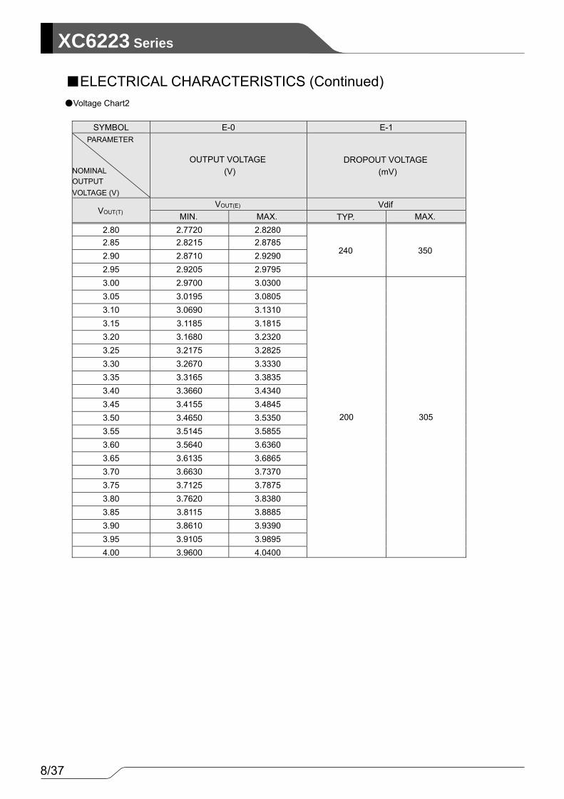
SYMBOL E-0 E-1 PARAMETER
NOMINAL OUTPUT VOLTAGE (V)
OUTPUT VOLTAGE
(V) DROPOUT VOLTAGE
(mV)
VOUT(T) VOUT(E) Vdif
MIN. MAX. TYP. MAX. 2.80 2.7720 2.8280
240 350 2.85 2.8215 2.8785 2.90 2.8710 2.9290 2.95 2.9205 2.9795 3.00 2.9700 3.0300
200 305
3.05 3.0195 3.0805 3.10 3.0690 3.1310 3.15 3.1185 3.1815 3.20 3.1680 3.2320 3.25 3.2175 3.2825 3.30 3.2670 3.3330 3.35 3.3165 3.3835 3.40 3.3660 3.4340 3.45 3.4155 3.4845 3.50 3.4650 3.5350 3.55 3.5145 3.5855 3.60 3.5640 3.6360 3.65 3.6135 3.6865 3.70 3.6630 3.7370 3.75 3.7125 3.7875 3.80 3.7620 3.8380 3.85 3.8115 3.8885 3.90 3.8610 3.9390 3.95 3.9105 3.9895 4.00 3.9600 4.0400
Voltage Chart2
ELECTRICAL CHARACTERISTICS (Continued)
9/37
XC6223Series
OPERATIONAL EXPLANATION
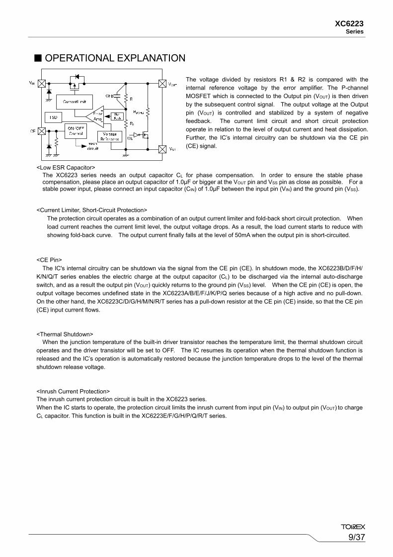
<Low ESR Capacitor> The XC6223 series needs an output capacitor CL for phase compensation. In order to ensure the stable phase compensation, please place an output capacitor of 1.0μF or bigger at the VOUT pin and VSS pin as close as possible. For a stable power input, please connect an input capacitor (CIN) of 1.0μF between the input pin (VIN) and the ground pin (VSS).
<Current Limiter, Short-Circuit Protection> The protection circuit operates as a combination of an output current limiter and fold-back short circuit protection. When load current reaches the current limit level, the output voltage drops. As a result, the load current starts to reduce with showing fold-back curve. The output current finally falls at the level of 50mA when the output pin is short-circuited.
<CE Pin> The IC's internal circuitry can be shutdown via the signal from the CE pin (CE). In shutdown mode, the XC6223B/D/F/H/
K/N/Q/T series enables the electric charge at the output capacitor (CL) to be discharged via the internal auto-discharge switch, and as a result the output pin (VOUT) quickly returns to the ground pin (VSS) level. When the CE pin (CE) is open, the output voltage becomes undefined state in the XC6223A/B/E/F/J/K/P/Q series because of a high active and no pull-down. On the other hand, the XC6223C/D/G/H/M/N/R/T series has a pull-down resistor at the CE pin (CE) inside, so that the CE pin (CE) input current flows.
<Thermal Shutdown> When the junction temperature of the built-in driver transistor reaches the temperature limit, the thermal shutdown circuit
operates and the driver transistor will be set to OFF. The IC resumes its operation when the thermal shutdown function is released and the IC’s operation is automatically restored because the junction temperature drops to the level of the thermal shutdown release voltage.
<Inrush Current Protection> The inrush current protection circuit is built in the XC6223 series. When the IC starts to operate, the protection circuit limits the inrush current from input pin (VIN) to output pin (VOUT) to charge CL capacitor. This function is built in the XC6223E/F/G/H/P/Q/R/T series.
The voltage divided by resistors R1 & R2 is compared with the internal reference voltage by the error amplifier. The P-channel MOSFET which is connected to the Output pin (VOUT) is then driven by the subsequent control signal. The output voltage at the Output pin (VOUT) is controlled and stabilized by a system of negative feedback. The current limit circuit and short circuit protection operate in relation to the level of output current and heat dissipation. Further, the IC’s internal circuitry can be shutdown via the CE pin (CE) signal.

10/37
XC6223 Series
NOTES ON USE 1. Where wiring impedance is high, operations may become unstable due to the noise and/or phase lag depending on output
current. Please strengthen input pin (VIN) and output pin (VOUT) wiring in particular. 2. The input capacitor CIN and the output capacitor CL should be placed to the as close as possible with a shorter wiring. 3. The IC is controlled with constant current start-up. Start-up sequence control is requested to draw a load current after
even nominal output voltage rising up the output voltage. 4. For temporary, transitional voltage drop or voltage rising phenomenon, the IC is liable to malfunction should the ratings be
exceeded. 5. Torex places an importance on improving our products and its reliability. However, by any possibility, we would request user fail-safe design and post-aging treatment on system or equipment.
11/37
XC6223Series
・測定回路2
・測定回路1
IOUT
V
A
V
・測定回路3
IOUT=30mA
V V
A
A
CIN=0.1μF(ceramic)
VIN
CEVSS
VOUT
CL
(ceramic)CIN
(ceramic)
VIN
CEVSS
VOUT
CIN
(ceramic)
CL
(ceramic)
VIN
CEVSS
VOUT
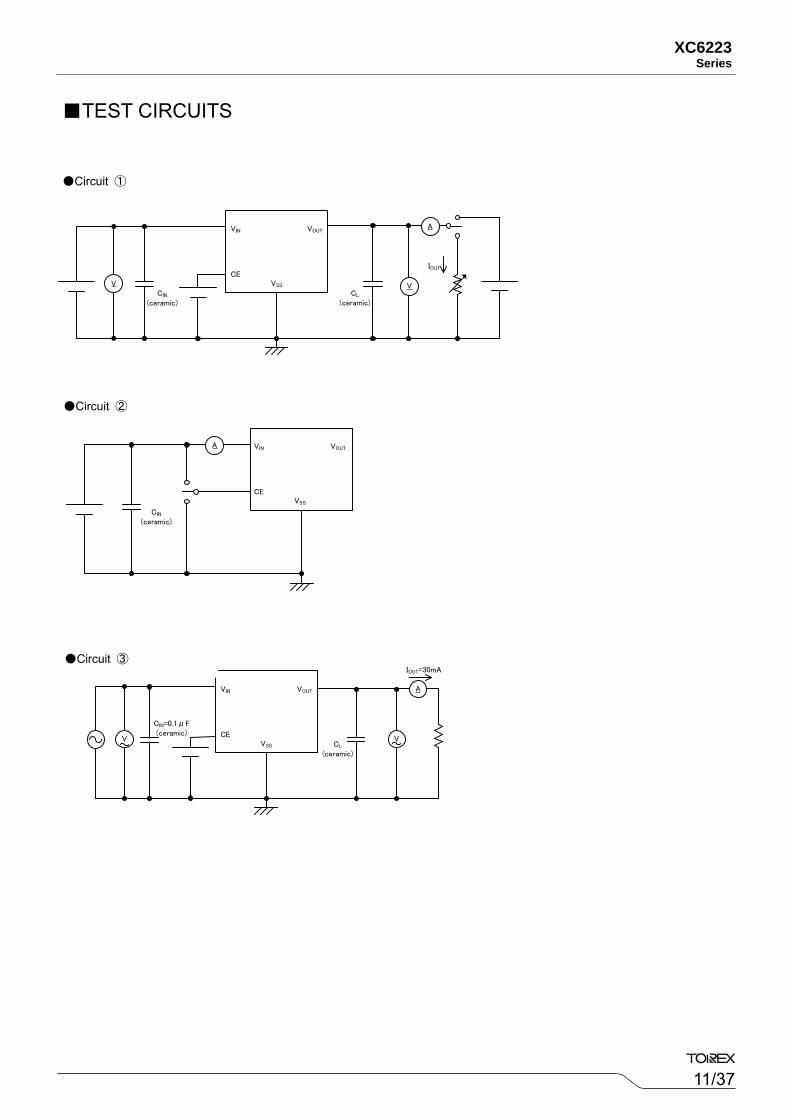
TEST CIRCUITS
Circuit ①
Circuit ②
Circuit ③
12/37
XC6223 Series
・測定回路4
A
V
V
CL=1μF(ceramic)
A
・測定回路5
VIN
CEVSS
VOUT
VIN
CEVSS
VOUT
CIN
(ceramic)
CIN
(ceramic)
CL
(ceramic)
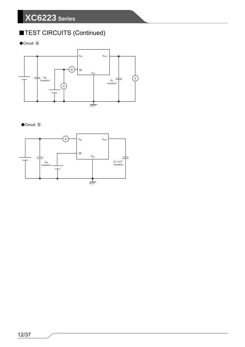
TEST CIRCUITS (Continued)Circuit ④
Circuit ⑤
13/37
XC6223Series
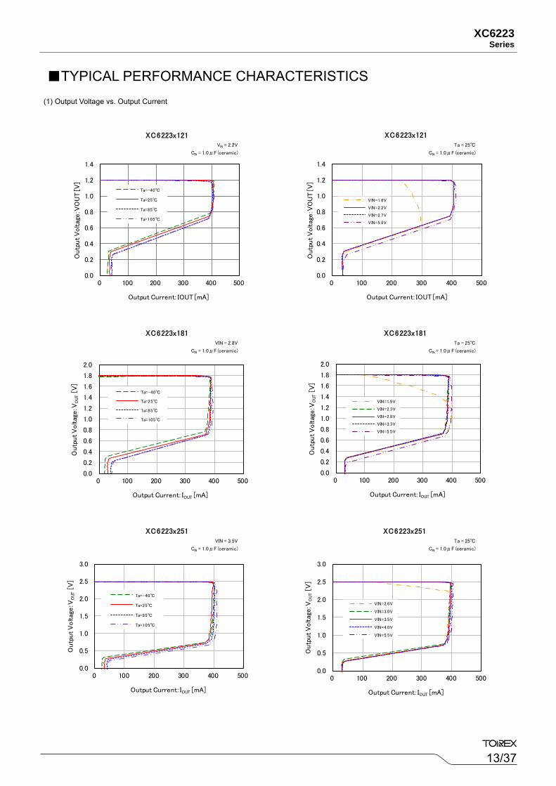
(1) Output Voltage vs. Output Current
TYPICAL PERFORMANCE CHARACTERISTICS
Ta = 25
CIN = 1.0μF (ceramic)
Ta = 25
CIN = 1.0μF (ceramic)
Ta = 25
CIN = 1.0μF (ceramic)
VIN = 3.5V
CIN = 1.0μF (ceramic)
VIN = 2.8V
CIN = 1.0μF (ceramic)
VIN = 2.2V
CIN = 1.0μF (ceramic)
0.0
0.2
0.4
0.6
0.8
1.0
1.2
1.4
1.6
1.8
2.0
0 100 200 300 400 500
Outp
ut V
oltag
e: V
OUT
[V]
Output Current: IOUT [mA]
XC6223x181
VIN=1.9V
VIN=2.3V
VIN=2.8V
VIN=3.3V
VIN=5.5V
0.0
0.5
1.0
1.5
2.0
2.5
3.0
0 100 200 300 400 500
Outp
ut V
oltag
e: V
OUT
[V]
Output Current: IOUT [mA]
XC6223x251
VIN=2.6V
VIN=3.0V
VIN=3.5V
VIN=4.0V
VIN=5.5V
0.0
0.5
1.0
1.5
2.0
2.5
3.0
0 100 200 300 400 500
Outp
ut V
oltag
e: V
OUT
[V]
Output Current: IOUT [mA]
XC6223x251
Ta=-40
Ta=25
Ta=85
Ta=105
0.0
0.2
0.4
0.6
0.8
1.0
1.2
1.4
0 100 200 300 400 500
Outp
ut V
oltag
e: V
OU
T [V
]
Output Current: IOUT [mA]
XC6223x121
Ta=-40
Ta=25
Ta=85
Ta=105
0.0
0.2
0.4
0.6
0.8
1.0
1.2
1.4
0 100 200 300 400 500
Outp
ut V
oltag
e: V
OU
T [V
]
Output Current: IOUT [mA]
XC6223x121
VIN=1.6V
VIN=2.2V
VIN=2.7V
VIN=5.5V
0.0
0.2
0.4
0.6
0.8
1.0
1.2
1.4
1.6
1.8
2.0
0 100 200 300 400 500
Outp
ut V
oltag
e: V
OUT
[V]
Output Current: IOUT [mA]
XC6223x181
Ta=-40
Ta=25
Ta=85
Ta=105
14/37
XC6223 Series
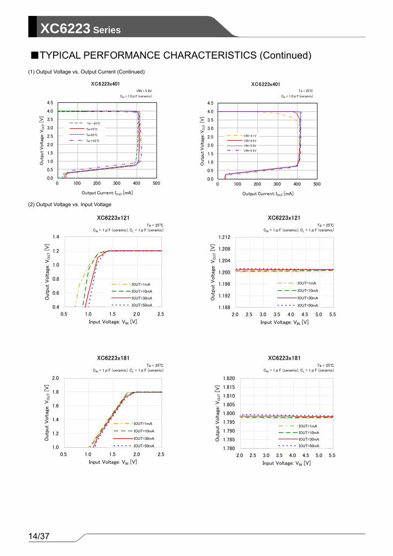
(1) Output Voltage vs. Output Current (Continued) (2) Output Voltage vs. Input Voltage
TYPICAL PERFORMANCE CHARACTERISTICS (Continued)
Ta = 25CIN = 1μF (ceramic), CL = 1μF (ceramic)
Ta = 25CIN = 1μF (ceramic), CL = 1μF (ceramic)
Ta = 25CIN = 1μF (ceramic), CL = 1μF (ceramic)
Ta = 25CIN = 1μF (ceramic), CL = 1μF (ceramic)
XC6223x121
0.4
0.6
0.8
1.0
1.2
1.4
0.5 1.0 1.5 2.0 2.5
Input Voltage: VIN [V]
Outp
ut
Voltag
e: V
OU
T [
V]
IOUT=1mA
IOUT=10mA
IOUT=30mA
IOUT=50mA
XC6223x121
1.188
1.192
1.196
1.200
1.204
1.208
1.212
2.0 2.5 3.0 3.5 4.0 4.5 5.0 5.5
Input Voltage: VIN [V]
Outp
ut
Voltag
e: V
OU
T [
V]
IOUT=1mA
IOUT=10mA
IOUT=30mA
IOUT=50mA
XC6223x181
1.0
1.2
1.4
1.6
1.8
2.0
0.5 1.0 1.5 2.0 2.5
Input Voltage: VIN [V]
Outp
ut
Voltag
e: V
OU
T [
V]
IOUT=1mA
IOUT=10mA
IOUT=30mA
IOUT=50mA
XC6223x181
1.780
1.785
1.790
1.795
1.800
1.805
1.810
1.815
1.820
2.0 2.5 3.0 3.5 4.0 4.5 5.0 5.5
Input Voltage: VIN [V]
Outp
ut
Voltag
e: V
OU
T [
V]
IOUT=1mA
IOUT=10mA
IOUT=30mA
IOUT=50mA
Ta = 25
CIN = 1.0μF (ceramic)
VIN = 5.0V
CIN = 1.0μF (ceramic)
0.0
0.5
1.0
1.5
2.0
2.5
3.0
3.5
4.0
4.5
0 100 200 300 400 500
Outp
ut V
oltag
e: V
OUT
[V]
Output Current: IOUT [mA]
XC6223x401
Ta=-40
Ta=25
Ta=85
Ta=105
0.0
0.5
1.0
1.5
2.0
2.5
3.0
3.5
4.0
4.5
0 100 200 300 400 500
Outp
ut V
oltag
e: V
OUT
[V]
Output Current: IOUT [mA]
XC6223x401
VIN=4.1V
VIN=4.5V
VIN=5.0V
VIN=5.5V
15/37
XC6223Series
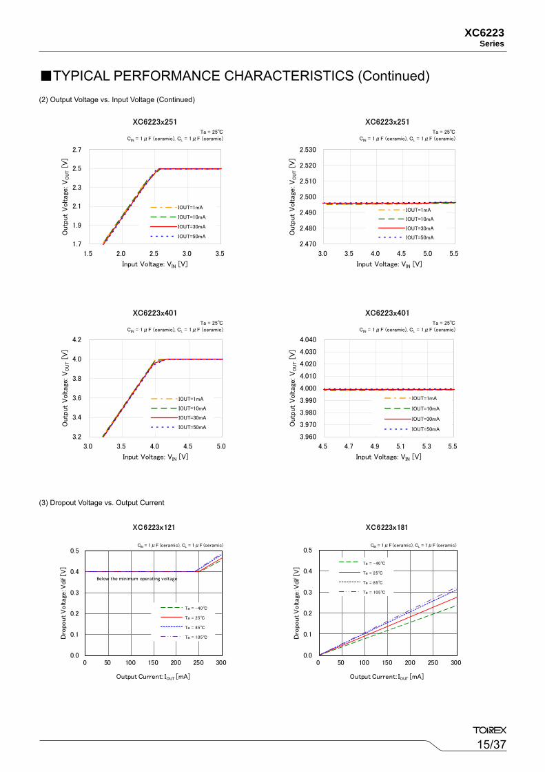
(2) Output Voltage vs. Input Voltage (Continued)
(3) Dropout Voltage vs. Output Current
Ta = 25CIN = 1μF (ceramic), CL = 1μF (ceramic)
Ta = 25CIN = 1μF (ceramic), CL = 1μF (ceramic)
Ta = 25CIN = 1μF (ceramic), CL = 1μF (ceramic)
Ta = 25CIN = 1μF (ceramic), CL = 1μF (ceramic)
XC6223x251
1.7
1.9
2.1
2.3
2.5
2.7
1.5 2.0 2.5 3.0 3.5
Input Voltage: VIN [V]
Outp
ut
Voltag
e: V
OU
T [
V]
IOUT=1mA
IOUT=10mA
IOUT=30mA
IOUT=50mA
XC6223x251
2.470
2.480
2.490
2.500
2.510
2.520
2.530
3.0 3.5 4.0 4.5 5.0 5.5
Input Voltage: VIN [V]
Outp
ut
Voltag
e: V
OU
T [
V]
IOUT=1mA
IOUT=10mA
IOUT=30mA
IOUT=50mA
XC6223x401
3.2
3.4
3.6
3.8
4.0
4.2
3.0 3.5 4.0 4.5 5.0
Input Voltage: VIN [V]
Outp
ut
Voltag
e: V
OU
T [
V]
IOUT=1mA
IOUT=10mA
IOUT=30mA
IOUT=50mA
XC6223x401
3.960
3.970
3.980
3.990
4.000
4.010
4.020
4.030
4.040
4.5 4.7 4.9 5.1 5.3 5.5
Input Voltage: VIN [V]
Outp
ut
Voltag
e: V
OU
T [
V]
IOUT=1mA
IOUT=10mA
IOUT=30mA
IOUT=50mA
TYPICAL PERFORMANCE CHARACTERISTICS (Continued)
CIN = 1μF (ceramic), CL = 1μF (ceramic) CIN = 1μF (ceramic), CL = 1μF (ceramic)
0.0
0.1
0.2
0.3
0.4
0.5
0 50 100 150 200 250 300
Dro
pout V
oltag
e: V
dif [V
]
Output Current: IOUT [mA]
XC6223x181
Ta = -40
Ta = 25
Ta = 85
Ta = 105
0.0
0.1
0.2
0.3
0.4
0.5
0 50 100 150 200 250 300
Dro
pout V
oltag
e: V
dif [V
]
Output Current: IOUT [mA]
XC6223x121
Ta = -40
Ta = 25
Ta = 85
Ta = 105
Below the minimum operating voltage

16/37
XC6223 Series
(3) Dropout Voltage vs. Output Current (Continued) (4) Supply Current vs. Input Voltage
TYPICAL PERFORMANCE CHARACTERISTICS (Continued)
CIN = 1μF (ceramic), CL = 1μF (ceramic)CIN = 1μF (ceramic), CL = 1μF (ceramic)
0.0
0.1
0.2
0.3
0.4
0.5
0 50 100 150 200 250 300
Dro
pout V
oltag
e: V
dif [V
]
Output Current: IOUT [mA]
XC6223x251
Ta = -40
Ta = 25
Ta = 85
Ta = 105
0.0
0.1
0.2
0.3
0.4
0.5
0 50 100 150 200 250 300
Dro
pout V
oltag
e: V
dif [V
]
Output Current: IOUT [mA]
XC6223x401
Ta = -40
Ta = 25
Ta = 85
Ta = 105
0
20
40
60
80
100
120
140
160
0 0.5 1 1.5 2 2.5 3 3.5 4 4.5 5 5.5
Supp
ly C
urr
ent: I S
S[μ
A]
Input Voltage: VIN [V]
XC6223x251
Ta = -40
Ta = 25
Ta = 85
Ta = 105
0
50
100
150
200
250
300
0 0.5 1 1.5 2 2.5 3 3.5 4 4.5 5 5.5
Supp
ly C
urr
ent: I S
S[μ
A]
Input Voltage: VIN [V]
XC6223x401
Ta = -40
Ta = 25
Ta = 85
Ta = 105
0
20
40
60
80
100
120
140
160
0 0.5 1 1.5 2 2.5 3 3.5 4 4.5 5 5.5
Supp
ly C
urr
ent: I S
S[μ
A]
Input Voltage: VIN [V]
XC6223x121
Ta = -40
Ta = 25
Ta = 85
Ta = 105
0
20
40
60
80
100
120
140
160
0 0.5 1 1.5 2 2.5 3 3.5 4 4.5 5 5.5
Supp
ly C
urr
ent: I S
S[μ
A]
Input Voltage: VIN [V]
XC6223x181
Ta = -40
Ta = 25
Ta = 85
Ta = 105
17/37
XC6223Series
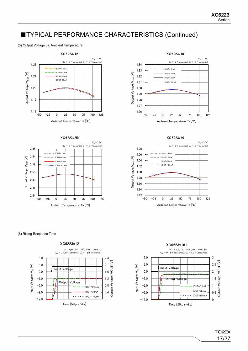
(5) Output Voltage vs. Ambient Temperature (6) Rising Response Time
tr = 5μs, Ta = 25,VIN = 0→2.8VCIN = 0.1μF (ceramic), CL = 1μF (ceramic)
tr = 5μs, Ta = 25,VIN = 0→2.2VCIN = 0.1μF (ceramic), CL = 1μF (ceramic)
XC6223x121
-12.0
-9.0
-6.0
-3.0
0.0
3.0
6.0
Time [50μs/div]
Inpu
t V
oltag
e: V
IN [
V]
0
0.4
0.8
1.2
1.6
2
2.4
Outp
ut
Voltag
e: V
OU
T [
V]
IOUT=0.1mA
IOUT=30mA
IOUT=100mA
XC6223x181
-12.0
-9.0
-6.0
-3.0
0.0
3.0
6.0
Time [50μs/div]
Inpu
t V
oltag
e: V
IN [
V]
0
0.5
1
1.5
2
2.5
3
Outp
ut
Voltag
e: V
OU
T [
V]
IOUT=0.1mA
IOUT=30mA
IOUT=100mA
Input Voltage
Output Voltage
Input Voltage
Output Voltage
TYPICAL PERFORMANCE CHARACTERISTICS (Continued)
VIN = 2.8V
CIN = 1μF (ceramic), CL = 1μF (ceramic)
VIN = 2.2V
CIN = 1μF (ceramic), CL = 1μF (ceramic)
1.18
1.19
1.20
1.21
1.22
-50 -25 0 25 50 75 100 125
Outp
ut V
oltag
e: V
OUT
[V]
Ambient Temperature: Ta []
XC6223x121
IOUT= 1mA
IOUT=10mA
IOUT=30mA
IOUT=50mA
1.76
1.77
1.78
1.79
1.80
1.81
1.82
1.83
1.84
-50 -25 0 25 50 75 100 125
Outp
ut V
oltag
e: V
OUT
[V]
Ambient Temperature: Ta []
XC6223x181
IOUT= 1mA
IOUT=10mA
IOUT=30mA
IOUT=100mA
VIN = 3.5V
CIN = 1μF (ceramic), CL = 1μF (ceramic)
VIN = 5.0V
CIN = 1μF (ceramic), CL = 1μF (ceramic)
3.92
3.94
3.96
3.98
4.00
4.02
4.04
4.06
4.08
-50 -25 0 25 50 75 100 125
Outp
ut V
oltag
e: V
OUT
[V]
Ambient Temperature: Ta []
XC6223x401
IOUT= 1mA
IOUT=10mA
IOUT=30mA
IOUT=100mA
2.44
2.46
2.48
2.50
2.52
2.54
2.56
-50 -25 0 25 50 75 100 125
Outp
ut V
oltag
e: V
OUT
[V]
Ambient Temperature: Ta []
XC6223x251
IOUT= 1mA
IOUT=10mA
IOUT=30mA
IOUT=100mA

18/37
XC6223 Series
(6) Rising Response Time (Continued)
(7) Input Transient Response
tr = tf = 5μs, Ta = 25, VIN = 2.2V⇔3.2VCIN = 0.1μF (ceramic), CL = 1.0μF (ceramic)
tr = tf = 5μs, Ta = 25, VIN = 2.8V⇔3.8VCIN = 0.1μF (ceramic), CL = 1.0μF (ceramic)
tr = tf = 5μs, Ta = 25, VIN = 3.5V⇔4.5VCIN = 0.1μF (ceramic), CL = 1.0μF (ceramic)
tr = tf = 5μs, Ta = 25, VIN = 4.5V⇔5.5VCIN = 0.1μF (ceramic), CL = 1.0μF (ceramic)
XC6223x401
0.0
1.0
2.0
3.0
4.0
5.0
6.0
Time [100μs/div]
Inpu
t V
oltag
e: V
IN [
V]
3.98
3.99
4
4.01
4.02
4.03
4.04
IOUT=10mA
IOUT=30mA
IOUT=100mA
XC6223x251
0.0
1.0
2.0
3.0
4.0
5.0
6.0
Time [100μs/div]
Inpu
t V
oltag
e: V
IN [
V]
2.48
2.49
2.5
2.51
2.52
2.53
2.54
IOUT=0.1mA
IOUT=30mA
IOUT=100mA
XC6223x181
-1.0
0.0
1.0
2.0
3.0
4.0
5.0
Time [100μs/div]
Inpu
t V
oltag
e: V
IN [
V]
1.79
1.8
1.81
1.82
1.83
1.84
1.85
IOUT=0.1mA
IOUT=30mA
IOUT=100mA
Input Voltage
Output Voltage
Input Voltage
Output Voltage
XC6223x121
-1.0
0.0
1.0
2.0
3.0
4.0
5.0
Time [100μs/div]
Inpu
t V
oltag
e: V
IN [
V]
1.18
1.19
1.2
1.21
1.22
1.23
1.24
Outp
ut
Voltag
e: V
OU
T [
V]
IOUT=0.1mA
IOUT=30mA
IOUT=100mA
Input Voltage
Output Voltage
Input Voltage
Output Voltage
tr = 5μs, Ta = 25,VIN = 0→3.5VCIN = 0.1μF (ceramic), CL = 1μF (ceramic)
tr = 5μs, Ta = 25,VIN = 0→5.0VCIN = 0.1μF (ceramic), CL = 1μF (ceramic)
XC6223x251
-12.0
-9.0
-6.0
-3.0
0.0
3.0
6.0
Time [50μs/div]
Inpu
t V
oltag
e: V
IN [
V]
0.0
1.0
2.0
3.0
4.0
5.0
6.0
Outp
ut
Voltag
e: V
OU
T [
V]
IOUT=0.1mA
IOUT=30mA
IOUT=100mA
XC6223x401
-12.0
-9.0
-6.0
-3.0
0.0
3.0
6.0
Time [50μs/div]
Inpu
t V
oltag
e: V
IN [
V]
0.0
1.0
2.0
3.0
4.0
5.0
6.0
Outp
ut
Voltag
e: V
OU
T [
V]
IOUT=0.1mA
IOUT=30mA
IOUT=100mA
Input Voltage
Output Voltage
Input Voltage
Output Voltage
TYPICAL PERFORMANCE CHARACTERISTICS (Continued)

19/37
XC6223Series
(8) Load Transient Response (tr=tf=0.5μs)
tr = tf = 0.5μs, Ta = 25, IOUT = 1⇔150mA
VIN = 2.2V, CIN = 1μF (ceramic), CL = 1μF (ceramic)
tr = tf = 0.5μs, Ta = 25, IOUT = 50⇔100mA
VIN = 2.2V, CIN = 1μF (ceramic), CL = 1μF (ceramic)
tr = tf = 0.5μs, Ta = 25, IOUT = 1⇔150mA
VIN = 2.8V, CIN = 1μF (ceramic), CL = 1μF (ceramic)
tr = tf = 0.5μs, Ta = 25, IOUT = 50⇔100mA
VIN = 2.8V, CIN = 1μF (ceramic), CL = 1μF (ceramic)
tr = tf = 0.5μs, Ta = 25, IOUT = 1⇔150mA
VIN = 3.5V, CIN = 1μF (ceramic), CL = 1μF (ceramic)
tr = tf = 0.5μs, Ta = 25, IOUT = 50⇔100mA
VIN = 3.5V, CIN = 1μF (ceramic), CL = 1μF (ceramic)
XC6223x251
2.44
2.45
2.46
2.47
2.48
2.49
2.50
2.51
2.52
Time [20μs/div]
Outp
ut
Voltag
e: V
OU
T [
V]
0
50
100
150
200
250
300
350
400
Outp
ut
Curr
ent
Iout[
mA
]
Output Voltage
Output Current
XC6223x121
0.90
0.95
1.00
1.05
1.10
1.15
1.20
1.25
1.30
Time [20μs/div]
Outp
ut
Voltag
e: V
OU
T [
V]
0
50
100
150
200
250
300
350
400
Outp
ut
Curr
ent
Iout[
mA
]
Output Voltage
Output Current
XC6223x121
1.14
1.15
1.16
1.17
1.18
1.19
1.20
1.21
1.22
Time [20μs/div]
Outp
ut
Voltag
e: V
OU
T [
V]
0
50
100
150
200
250
300
350
400
Outp
ut
Curr
ent
Iout[
mA
]
Output Voltage
Output Current
XC6223x181
1.50
1.55
1.60
1.65
1.70
1.75
1.80
1.85
1.90
Time [20μs/div]
Outp
ut
Voltag
e: V
OU
T [
V]
0
50
100
150
200
250
300
350
400
Outp
ut
Curr
ent
Iout[
mA
]
Output Voltage
Output Current
XC6223x181
1.74
1.75
1.76
1.77
1.78
1.79
1.80
1.81
1.82
Time [20μs/div]
Outp
ut
Voltag
e: V
OU
T [
V]
0
50
100
150
200
250
300
350
400
Outp
ut
Curr
ent
Iout[
mA
]
Output Voltage
Output Current
XC6223x251
2.20
2.25
2.30
2.35
2.40
2.45
2.50
2.55
2.60
Time [20μs/div]
Outp
ut
Voltag
e: V
OU
T [
V]
0
50
100
150
200
250
300
350
400
Outp
ut
Curr
ent
Iout[
mA
]
Output Voltage
Output Current
TYPICAL PERFORMANCE CHARACTERISTICS (Continued)

20/37
XC6223 Series
(8) Load Transient Response (tr=tf=0.5μs) (Continued)
(8) Load Transient Response (tr=tf=5μs) (Continued)
tr = tf = 5μs, Ta = 25, IOUT = 50⇔100mA
VIN = 2.8V, CIN = 1μF (ceramic), CL = 1μF (ceramic)
tr = tf = 5μs, Ta = 25, IOUT = 1⇔150mA
VIN = 2.8V, CIN = 1μF (ceramic), CL = 1μF (ceramic)
tr = tf = 5μs, Ta = 25, IOUT = 1⇔150mA
VIN = 2.2V, CIN = 1μF (ceramic), CL = 1μF (ceramic)
tr = tf = 5μs, Ta = 25, IOUT = 50⇔100mA
VIN = 2.2V, CIN = 1μF (ceramic), CL = 1μF (ceramic)
XC6223x121
1.14
1.15
1.16
1.17
1.18
1.19
1.20
1.21
1.22
Time [50μs/div]
Outp
ut
Voltag
e: V
OU
T [
V]
0
50
100
150
200
250
300
350
400
Outp
ut
Curr
ent
Iout[
mA
]
Output Voltage
Output Current
XC6223x181
1.74
1.75
1.76
1.77
1.78
1.79
1.80
1.81
1.82
Time [50μs/div]
Outp
ut
Voltag
e: V
OU
T [
V]
0
50
100
150
200
250
300
350
400
Outp
ut
Curr
ent
Iout[
mA
]
Output Voltage
Output Current
XC6223x121
1.14
1.15
1.16
1.17
1.18
1.19
1.20
1.21
1.22
Time [50μs/div]
Outp
ut
Voltag
e: V
OU
T [
V]
0
50
100
150
200
250
300
350
400
Outp
ut
Curr
ent
Iout[
mA
]
Output Voltage
Output Current
XC6223x181
1.74
1.75
1.76
1.77
1.78
1.79
1.80
1.81
1.82
Time [50μs/div]
Outp
ut
Voltag
e: V
OU
T [
V]
0
50
100
150
200
250
300
350
400
Outp
ut
Curr
ent
Iout[
mA
]
Output Current
Output Voltage
tr = tf = 0.5μs, Ta = 25, IOUT =50⇔100mA
VIN = 5.0V, CIN = 1μF (ceramic), CL = 1μF (ceramic)
tr = tf = 0.5μs, Ta = 25, IOUT = 1⇔150mA
VIN = 5.0V, CIN = 1μF (ceramic), CL = 1μF (ceramic)
XC6223x401
3.94
3.95
3.96
3.97
3.98
3.99
4.00
4.01
4.02
Time [20μs/div]
Outp
ut
Voltag
e: V
OU
T [
V]
0
50
100
150
200
250
300
350
400
450
500
Outp
ut
Curr
ent
Iout[
mA
]
Output Voltage
Output Current
XC6223x401
3.70
3.75
3.80
3.85
3.90
3.95
4.00
4.05
4.10
Time [20μs/div]
Outp
ut
Voltag
e: V
OU
T [
V]
0
50
100
150
200
250
300
350
400
Outp
ut
Curr
ent
Iout[
mA
]
Output Voltage
Output Current
TYPICAL PERFORMANCE CHARACTERISTICS (Continued)
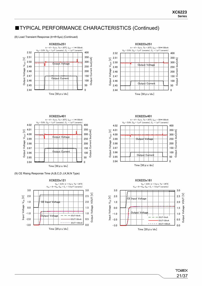
21/37
XC6223Series
(8) Load Transient Response (tr=tf=5μs) (Continued)
(9) CE Rising Response Time (A,B,C,D J,K,M,N Type)
tr = tf = 5μs, Ta = 25, IOUT = 1⇔150mA
VIN = 5.0V, CIN = 1μF (ceramic), CL = 1μF (ceramic)
tr = tf = 5μs, Ta = 25, IOUT = 50⇔100mA
VIN = 5.0V, CIN = 1μF (ceramic), CL = 1μF (ceramic)
tr = tf = 5μs, Ta = 25, IOUT = 1⇔150mA
VIN = 3.5V, CIN = 1μF (ceramic), CL = 1μF (ceramic)
tr = tf = 5μs, Ta = 25, IOUT = 50⇔100mA
VIN = 3.5V, CIN = 1μF (ceramic), CL = 1μF (ceramic)
XC6223x251
2.44
2.45
2.46
2.47
2.48
2.49
2.50
2.51
2.52
Time [50μs/div]
Outp
ut
Voltag
e: V
OU
T [
V]
0
50
100
150
200
250
300
350
400
Outp
ut
Curr
ent
Iout[
mA
]
Output Voltage
Output Current
XC6223x401
3.94
3.95
3.96
3.97
3.98
3.99
4.00
4.01
4.02
Time [50μs/div]
Outp
ut
Voltag
e: V
OU
T [
V]
0
50
100
150
200
250
300
350
400
Outp
ut
Curr
ent
Iout[
mA
]
Output Voltage
Output Current
XC6223x251
2.44
2.45
2.46
2.47
2.48
2.49
2.50
2.51
2.52
Time [50μs/div]
Outp
ut
Voltag
e: V
OU
T [
V]
0
50
100
150
200
250
300
350
400
Outp
ut
Curr
ent
Iout[
mA
]
Output Voltage
Output Current
Output Voltage
Output Current
XC6223x401
3.94
3.95
3.96
3.97
3.98
3.99
4.00
4.01
4.02
Time [50μs/div]
Outp
ut
Voltag
e: V
OU
T [
V]
0
50
100
150
200
250
300
350
400
Outp
ut
Curr
ent
Iout[
mA
]
VIN = 2.2V, tr = 5μs, Ta = 25
VCE = 0→VIN, CIN = CL = 1.0μF (ceramic)
VIN = 2.8V, tr = 5μs, Ta = 25
VCE = 0→VIN, CIN = CL = 1.0μF (ceramic)
XC6223x181
-3.0
-2.0
-1.0
0.0
1.0
2.0
3.0
Time [20μs/div]
Inpu
t V
oltag
e: V
CE [
V]
0.0
0.5
1.0
1.5
2.0
2.5
3.0
Outp
ut
Voltag
e: V
OU
T [
V]
IOUT=0mA
IOUT=30mA
IOUT=100mA
CE Input Voltage
Output Voltage
XC6223x121
-3.0
-2.0
-1.0
0.0
1.0
2.0
3.0
Time [20μs/div]
Inpu
t V
oltag
e: V
CE [
V]
0.0
0.5
1.0
1.5
2.0
2.5
3.0
Outp
ut
Voltag
e: V
OU
T [
V]
IOUT=0mA
IOUT=30mA
IOUT=100mA
CE Input Voltage
Output Voltage
TYPICAL PERFORMANCE CHARACTERISTICS (Continued)
22/37
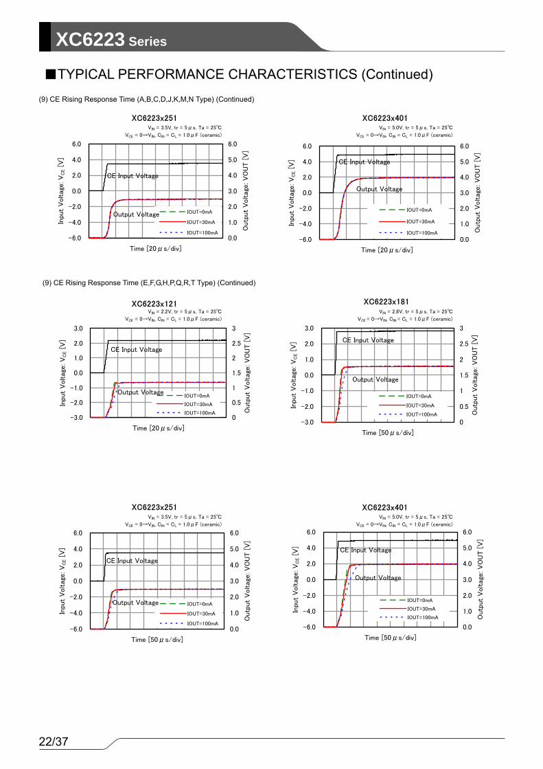
XC6223 Series
(9) CE Rising Response Time (A,B,C,D,J,K,M,N Type) (Continued)
(9) CE Rising Response Time (E,F,G,H,P,Q,R,T Type) (Continued)
VIN = 3.5V, tr = 5μs, Ta = 25
VCE = 0→VIN, CIN = CL = 1.0μF (ceramic)
VIN = 5.0V, tr = 5μs, Ta = 25
VCE = 0→VIN, CIN = CL = 1.0μF (ceramic)
XC6223x251
-6.0
-4.0
-2.0
0.0
2.0
4.0
6.0
Time [20μs/div]
Inpu
t V
oltag
e: V
CE [
V]
0.0
1.0
2.0
3.0
4.0
5.0
6.0
Outp
ut
Voltag
e: V
OU
T [
V]
IOUT=0mA
IOUT=30mA
IOUT=100mA
CE Input Voltage
Output Voltage
XC6223x401
-6.0
-4.0
-2.0
0.0
2.0
4.0
6.0
Time [20μs/div]
Inpu
t V
oltag
e: V
CE [
V]
0.0
1.0
2.0
3.0
4.0
5.0
6.0
Outp
ut
Voltag
e: V
OU
T [
V]
IOUT=0mA
IOUT=30mA
IOUT=100mA
CE Input Voltage
Output Voltage
VIN = 2.2V, tr = 5μs, Ta = 25
VCE = 0→VIN, CIN = CL = 1.0μF (ceramic)
VIN = 2.8V, tr = 5μs, Ta = 25
VCE = 0→VIN, CIN = CL = 1.0μF (ceramic)
VIN = 3.5V, tr = 5μs, Ta = 25
VCE = 0→VIN, CIN = CL = 1.0μF (ceramic)
VIN = 5.0V, tr = 5μs, Ta = 25
VCE = 0→VIN, CIN = CL = 1.0μF (ceramic)
XC6223x401
-6.0
-4.0
-2.0
0.0
2.0
4.0
6.0
Time [50μs/div]
Inpu
t V
oltag
e: V
CE [
V]
0.0
1.0
2.0
3.0
4.0
5.0
6.0
Outp
ut
Voltag
e: V
OU
T [
V]
IOUT=0mA
IOUT=30mA
IOUT=100mA
XC6223x251
-6.0
-4.0
-2.0
0.0
2.0
4.0
6.0
Time [50μs/div]
Inpu
t V
oltag
e: V
CE [
V]
0.0
1.0
2.0
3.0
4.0
5.0
6.0
Outp
ut
Voltag
e: V
OU
T [
V]
IOUT=0mA
IOUT=30mA
IOUT=100mA
XC6223x181
-3.0
-2.0
-1.0
0.0
1.0
2.0
3.0
Time [50μs/div]
Inpu
t V
oltag
e: V
CE [
V]
0
0.5
1
1.5
2
2.5
3
Outp
ut
Voltag
e: V
OU
T [
V]
IOUT=0mA
IOUT=30mA
IOUT=100mA
XC6223x121
-3.0
-2.0
-1.0
0.0
1.0
2.0
3.0
Time [20μs/div]
Inpu
t V
oltag
e: V
CE [
V]
0
0.5
1
1.5
2
2.5
3
Outp
ut
Voltag
e: V
OU
T [
V]
IOUT=0mA
IOUT=30mA
IOUT=100mA
CE Input Voltage
Output Voltage
CE Input Voltage
Output Voltage
CE Input Voltage
Output Voltage
CE Input Voltage
Output Voltage
TYPICAL PERFORMANCE CHARACTERISTICS (Continued)
23/37
XC6223Series
(10) Inrush Current Response Time (E,F,G,H,P,Q,R,T Type)
VIN = 2.2V, tr = 5μs, Ta = 25
VCE = 0→VIN, CIN = CL = 1.0μF (ceramic)
VIN = 2.8V, tr = 5μs, Ta = 25
VCE = 0→VIN, CIN = CL = 1.0μF (ceramic)
VIN = 3.5V, tr = 5μs, Ta = 25
VCE = 0→VIN, CIN = CL = 1.0μF (ceramic)
VIN = 5.0V, tr = 5μs, Ta = 25
VCE = 0→VIN, CIN = CL = 1.0μF (ceramic)
XC6223x401
-2.0
-1.0
0.0
1.0
2.0
3.0
4.0
5.0
6.0
Time [50μs/div]
Inpu
t V
oltag
e: V
CE [
V]
0
50
100
150
200
250
300
350
400
Rush
Curr
en: IR
USH
[m
A]
Rush Current
XC6223x251
-2.0
-1.0
0.0
1.0
2.0
3.0
4.0
5.0
6.0
Time [50μs/div]
Inpu
t V
oltag
e: V
CE [
V]
0
50
100
150
200
250
300
350
400
Rush
Curr
en: IR
USH
[m
A]
Rush Current
XC6223x181
-4.0
-3.0
-2.0
-1.0
0.0
1.0
2.0
3.0
4.0
Time [50μs/div]
Inpu
t V
oltag
e: V
CE [
V]
0
50
100
150
200
250
300
350
400
Rush
Curr
en: IR
USH
[m
A]
Rush Current
XC6223x121
-4.0
-3.0
-2.0
-1.0
0.0
1.0
2.0
3.0
4.0
Time [20μs/div]
Inpu
t V
oltag
e: V
CE [
V]
0
50
100
150
200
250
300
350
400
Rush
Curr
en: IR
USH
[m
A]
Rush Current
CE Input Voltage
Output Voltage
CE Input Voltage
Output Voltage
CE Input Voltage
Output Voltage
CE Input Voltage
Output Voltage
TYPICAL PERFORMANCE CHARACTERISTICS (Continued)

24/37
XC6223 Series (11) Ripple Rejection Rate
Ta = 25, VIN = 3.5VDC+0.5Vp-pAC
CIN = 0.1μF (ceramic), CL = 1μF (ceramic)
Ta = 25, VIN = 4.3VDC+0.5Vp-pAC
CIN = 0.1μF (ceramic), CL = 1μF (ceramic)
Ta = 25, VIN = 3.0VDC+0.5Vp-pAC
CIN = 0.1μF (ceramic), CL = 1μF (ceramic)
Ta = 25, VIN = 3.0VDC+0.5Vp-pAC
CIN = 0.1μF (ceramic), CL = 1μF (ceramic)
XC6223x121
0
20
40
60
80
100
0.01 0.1 1 10 100
Ripple Frequency: f [kHz]
Rip
ple R
eje
ction R
ate: R
R [
dB]
IOUT=0.1mA
IOUT=1mA
IOUT=30mA
XC6223x181
0
20
40
60
80
100
0.01 0.1 1 10 100
Ripple Frequency: f [kHz]
Rip
ple R
eje
ction R
ate: R
R [
dB]
IOUT=0.1mA
IOUT=1mA
IOUT=30mA
XC6223x251
0
20
40
60
80
100
0.01 0.1 1 10 100
Ripple Frequency: f [kHz]
Rip
ple R
eje
ction R
ate: R
R [
dB]
IOUT=0.1mA
IOUT=1mA
IOUT=30mA
XC6223x331
0
20
40
60
80
100
0.01 0.1 1 10 100
Ripple Frequency: f [kHz]
Rip
ple R
eje
ction R
ate: R
R [
dB]
IOUT=0.1mA
IOUT=1mA
IOUT=30mA
TYPICAL PERFORMANCE CHARACTERISTICS (Continued)

25/37
XC6223Series
(12) Output Noise Density
TYPICAL PERFORMANCE CHARACTERISTICS (Continued)
XC6223x121
0.01
0.1
1
10
100
0.1 1 10 100
Frequency : f [kHz]
Outp
ut
Nois
e D
ensi
ty : [
μV
/√
Hz]
IOUT=30mA
VIN=2.2V, Ta=25
CIN=CL=1.0μF(ceramic)
Frequency-Range : 0.1~100kHz Output Noise : 32.60μVrms
XC6223x181
0.01
0.1
1
10
100
0.1 1 10 100
Frequency : f [kHz]
Outp
ut
Nois
e D
ensi
ty : [
μV
/√
Hz]
IOUT=30mA
VIN=2.8, Ta=25
CIN=CL=1.0μF(ceramic)
Frequency-Range : 0.1~100kHz Output Noise : 49.74μVrms
XC6223x331
0.01
0.1
1
10
100
0.1 1 10 100
Frequency : f [kHz]
Outp
ut
Nois
e D
ensi
ty : [
μV
/√
Hz]
IOUT=30mA
VIN=5.0V, Ta=25
CIN=CL=1.0μF(ceramic)
Frequency-Range : 0.1~100kHz Output Noise : 81.52μVrms

26/37
XC6223 Series
PACKAGING INFORMATION
*The package don’t have filet because
side of lead is no plating.
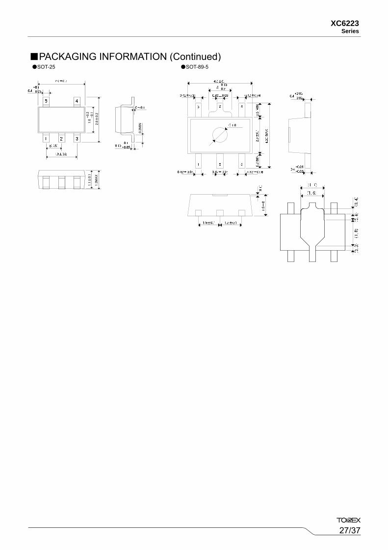
27/37
XC6223Series
PACKAGING INFORMATION (Continued)
1.6
+0.
2-0.
1
2.8
±0.2
1.1±
0.1
1.3M
AX
0.2M
IN
SOT-25 SOT-89-5

28/37
XC6223 Series
1.30
0.47
0.22 0.4
0.4
0.1
0.1
0.27
5
0.25
1.05
0.55
0.25
0.25
2.0
0.4
0.7
0.4
0.3
0.5
0.3
1.9
USPQ-4B03 Reference Pattern Layout USPQ-4B03 Reference Metal Mask Design
PACKAGING INFORMATION (Continued)
USP-4 Reference Pattern Layout USP-4 Reference Metal Mask Design
29/37
XC6223Series
USPQ-4B03 Power Dissipation
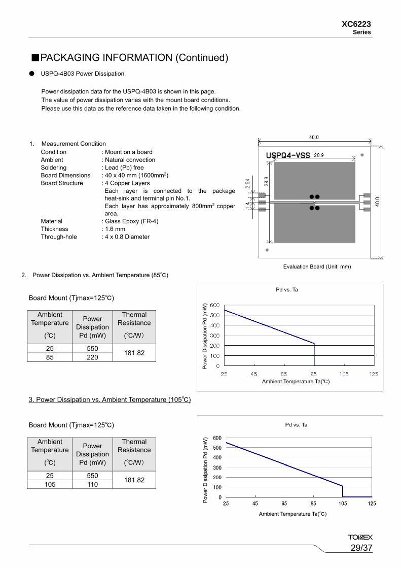
Board Mount (Tjmax=125)
3. Power Dissipation vs. Ambient Temperature (105)
Board Mount (Tjmax=125)
Ambient Temperature
()
Power Dissipation Pd (mW)
Thermal Resistance
(/W)
25 550 181.82 85 220
Ambient Temperature
()
Power Dissipation Pd (mW)
Thermal Resistance
(/W)
25 550 181.82 105 110
PACKAGING INFORMATION (Continued)
Power dissipation data for the USPQ-4B03 is shown in this page. The value of power dissipation varies with the mount board conditions. Please use this data as the reference data taken in the following condition.
2. Power Dissipation vs. Ambient Temperature (85) Evaluation Board (Unit: mm)
1. Measurement Condition Condition : Mount on a board Ambient : Natural convection Soldering : Lead (Pb) free Board Dimensions : 40 x 40 mm (1600mm2) Board Structure : 4 Copper Layers Each layer is connected to the package
heat-sink and terminal pin No.1. Each layer has approximately 800mm2 copper
area. Material : Glass Epoxy (FR-4) Thickness : 1.6 mm Through-hole : 4 x 0.8 Diameter
Pd vs. Ta
Ambient Temperature Ta()
Pd vs. Ta
Ambient Temperature Ta()
Pow
er D
issi
patio
n P
d (m
W)
Pow
er D
issi
patio
n P
d (m
W)

30/37
XC6223 Series
USP-4 Power Dissipation
2. Power Dissipation vs. Ambient Temperature (85)
Board Mount (Tjmax=125)
3. Power Dissipation vs. Ambient Temperature (105)
Board Mount (Tjmax=125)
Ambient Temperature
()
Power Dissipation Pd (mW)
Thermal Resistance
(/W)
25 1000 100.00 85 400
Ambient Temperature
()
Power Dissipation Pd (mW)
Thermal Resistance
(/W)
25 1000 100.00 105 200
PACKAGING INFORMATION (Continued)
Power dissipation data for the USP-4 is shown in this page. The value of power dissipation varies with the mount board conditions. Please use this data as the reference data taken in the following condition.
1. Measurement Condition Condition: Mount on a board Ambient: Natural convection Soldering: Lead (Pb) free Board: Dimensions 40 x 40 mm (1600 mm2 in one side)
Copper (Cu) traces occupy 50% of the board area In top and back faces Package heat-sink is tied to the copper traces
Material: Glass Epoxy (FR-4) Thickness: 1.6 mm Through-hole: 4 x 0.8 Diameter
Evaluation Board (Unit: mm)
Pd vs. Ta
Pow
er D
issi
patio
n P
d (m
W)
Pd vs. Ta
Ambient Temperature Ta()
Pow
er D
issi
patio
n P
d (m
W)
31/37
XC6223Series
SSOT-24 Power Dissipation
2. Power Dissipation vs. Ambient Temperature (85)
Board Mount (Tjmax=125)
3. Power Dissipation vs. Ambient Temperature (105)
Board Mount (Tjmax=125)
Ambient Temperature
()
Power Dissipation Pd (mW)
Thermal Resistance
(/W)
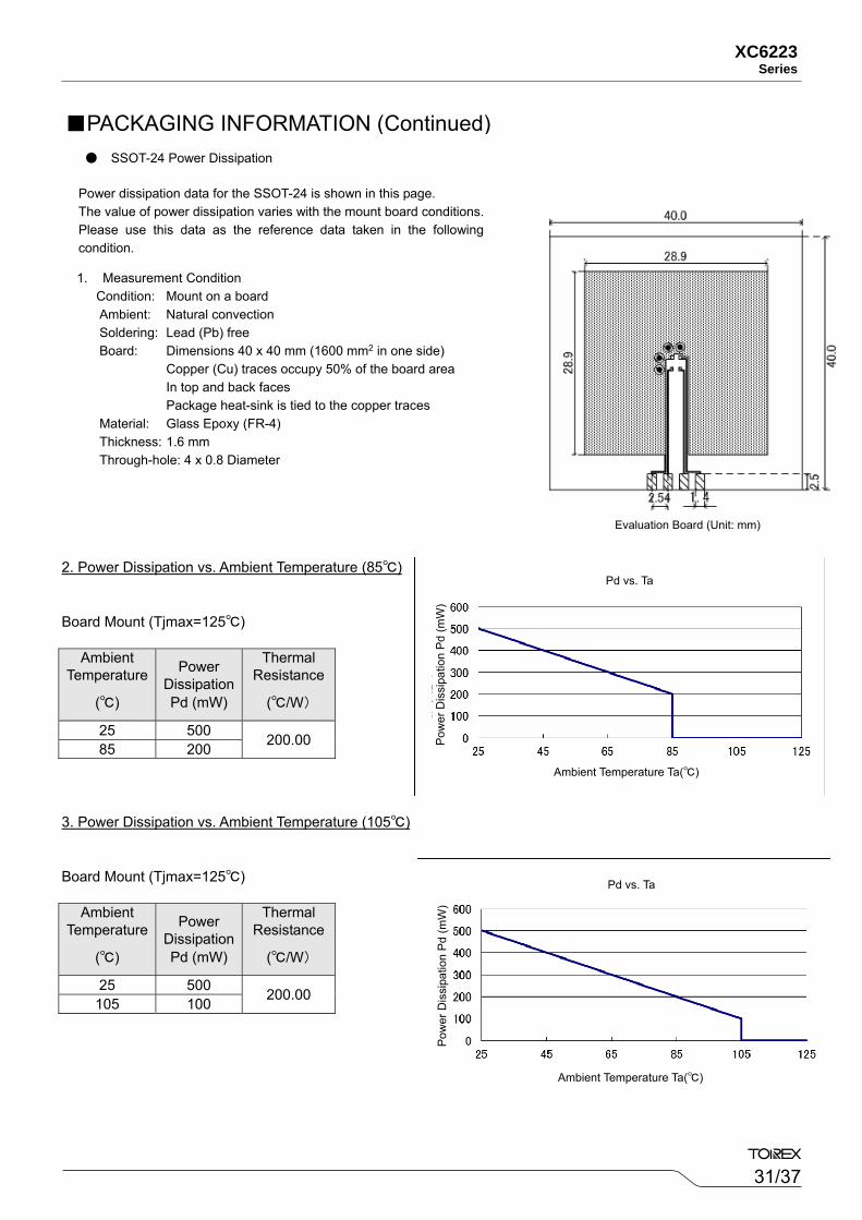
25 500 200.00 85 200
Ambient Temperature
()
Power Dissipation Pd (mW)
Thermal Resistance
(/W)
25 500 200.00 105 100
PACKAGING INFORMATION (Continued)
Power dissipation data for the SSOT-24 is shown in this page. The value of power dissipation varies with the mount board conditions.Please use this data as the reference data taken in the following condition.
1. Measurement Condition Condition: Mount on a board Ambient: Natural convection Soldering: Lead (Pb) free Board: Dimensions 40 x 40 mm (1600 mm2 in one side)
Copper (Cu) traces occupy 50% of the board area In top and back faces Package heat-sink is tied to the copper traces
Material: Glass Epoxy (FR-4) Thickness: 1.6 mm Through-hole: 4 x 0.8 Diameter
Evaluation Board (Unit: mm)
Pd vs. Ta
Pow
er D
issi
patio
n P
d (m
W)
Ambient Temperature Ta()
Pd vs. Ta
Pow
er D
issi
patio
n P
d (m
W)
Ambient Temperature Ta()

32/37
XC6223 Series
SOT-25 Power Dissipation
2. Power Dissipation vs. Ambient temperature(85)
Board Mount ( Tjmax=125)
3. Power Dissipation vs. Ambient temperature(105)
Board Mount ( Tjmax=125)
Ambient Temperature
()
Power Dissipation Pd (mW)
Thermal Resistance
(/W)
25 600 166.67 85 240
Ambient Temperature
()
Power Dissipation Pd (mW)
Thermal Resistance
(/W)
25 600 166.67 105 120
PACKAGING INFORMATION (Continued)
Power dissipation data for the SOT-25 is shown in this page. The value of power dissipation varies with the mount board conditions.Please use this data as the reference data taken in the following condition.
1. Measurement Condition Condition: Mount on a board Ambient: Natural convection Soldering: Lead (Pb) free Board: Dimensions 40 x 40 mm (1600 mm2 in one side)
Copper (Cu) traces occupy 50% of the board area In top and back faces Package heat-sink is tied to the copper traces (Board of SOT-26 is used.)
Material: Glass Epoxy (FR-4) Thickness: 1.6 mm Through-hole: 4 x 0.8 Diameter
評価基板レイアウト(単位:mm)Evaluation Board (Unit: mm)
Pd vs Ta
0
100
200
300
400
500
600
700
25 45 65 85 105 125
Ambient Temperature Ta()
Pow
er D
issi
pat
ion P
d(m
W)
Pd vs Ta
0
100
200
300
400
500
600
700
25 45 65 85 105 125
Ambient Temparature Ta()
Pow
er
Dis
sipa
tion P
d(m
W)
33/37
XC6223Series
SOT-89-5 Power Dissipation
2. Power Dissipation vs. Ambient temperature(85)
Board Mount (Tj max = 125)
Ambient Temperature
()
Power Dissipation Pd
(mW)
Thermal Resistance
(/W)
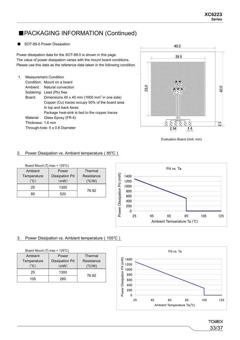
25 1300 76.92
85 520
3. Power Dissipation vs. Ambient temperature(105)
Board Mount (Tj max = 125)
Ambient Temperature
()
Power Dissipation Pd
(mW)
Thermal Resistance
(/W)
25 1300 76.92
105 260
Power dissipation data for the SOT-89-5 is shown in this page. The value of power dissipation varies with the mount board conditions. Please use this data as the reference data taken in the following condition.
1. Measurement Condition Condition: Mount on a board Ambient: Natural convection Soldering: Lead (Pb) free Board: Dimensions 40 x 40 mm (1600 mm2 in one side)
Copper (Cu) traces occupy 50% of the board area In top and back faces Package heat-sink is tied to the copper traces
Material: Glass Epoxy (FR-4) Thickness: 1.6 mm Through-hole: 5 x 0.8 Diameter
Evaluation Board (Unit: mm)
Pd-Ta特性グラフ
0
200
400
600
800
1000
1200
1400
25 45 65 85 105 125
周辺温度Ta()
許容
損失
Pd(m
W)
Pd vs. Ta
Ambient Temperature Ta ()
Pow
er D
issi
patio
n P
d (m
W)
て
PACKAGING INFORMATION (Continued)
Pd-Ta特性グラフ
0
200
400
600
800
1000
1200
1400
25 45 65 85 105 125
周囲温度Ta()
許容
損失
Pd(
mW
)
Pd vs. Ta
Pow
er D
issi
patio
n P
d (m
W)
Ambient Temperature Ta()

34/37
XC6223 Series
USPQ-4B03
MARK
PRODUCT SERIES OUTPUT VOLTAGE 0.1V INCREMENTS
OUTPUT VOLTAGE 0.05V INCREMENTS
VOLTAGE=1.2~3.9V VOLTAGE =4.0V VOLTAGE =1.25~3.95V0
H
8 XC6223A/J***** 1 9 XC6223B/K***** 2 A XC6223C/M***** 3 B XC6223D/N***** 4 C XC6223E/P***** 5 D XC6223F/Q***** 6 E XC6223G/R***** 7 F XC6223H/T*****
MARK OUTPUT VOLTAGE (V) MARK OUTPUT VOLTAGE (V)
0 - - F 2.50 2.55 1 - - H 2.60 2.65 2 1.20 1.25 K 2.70 2.75 3 1.30 1.35 L 2.80 2.85 4 1.40 1.45 M 2.90 2.95 5 1.50 1.55 N 3.00 3.05 6 1.60 1.65 P 3.10 3.15 7 1.70 1.75 R 3.20 3.25 8 1.80 1.85 S 3.30 3.35 9 1.90 1.95 T 3.40 3.45 A 2.00 2.05 U 3.50 3.55 B 2.10 2.15 V 3.60 3.65 C 2.20 2.25 X 3.70 3.75 D 2.30 2.35 Y 3.80 3.85 E 2.40 2.45 Z 3.90 3.95
PRODUCT SERIES MARKXC6223A/J***** 0 XC6223B/K***** 1 XC6223C/M***** 2 XC6223D/N***** 3 XC6223E/P***** 4 XC6223F/Q***** 5 XC6223G/R***** 6 XC6223H/T***** 7
MARKING RULE
① represents type of regulator and output voltage range.
② represents output voltage.
③④ represents production lot number. 01 to 09, 0A to 0Z, 11 to 9Z, A1 to A9, AA to Z9, ZA to ZZ in order. (G, I, J, O, Q, W excepted) *No character inversion used.
③ ④
① ②
1 2
4 3
VOLTAGE=1.2~3.95[V] VOLTAGE=4.0[V]
USPQ-4B03 (TOP VIEW)
35/37
XC6223Series
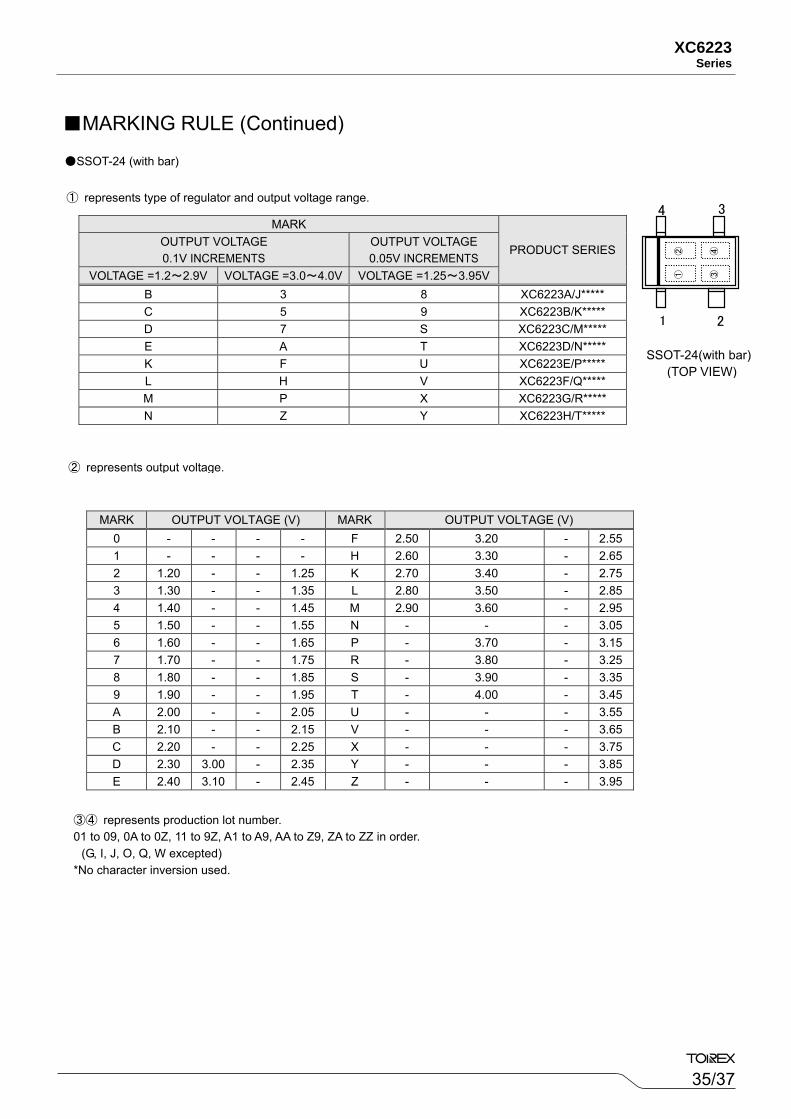
SSOT-24 (with bar)
MARK
PRODUCT SERIES OUTPUT VOLTAGE 0.1V INCREMENTS
OUTPUT VOLTAGE 0.05V INCREMENTS
VOLTAGE =1.2~2.9V VOLTAGE =3.0~4.0V VOLTAGE =1.25~3.95VB 3 8 XC6223A/J***** C 5 9 XC6223B/K***** D 7 S XC6223C/M***** E A T XC6223D/N***** K F U XC6223E/P***** L H V XC6223F/Q***** M P X XC6223G/R***** N Z Y XC6223H/T*****
MARK OUTPUT VOLTAGE (V) MARK OUTPUT VOLTAGE (V) 0 - - - - F 2.50 3.20 - 2.55 1 - - - - H 2.60 3.30 - 2.65 2 1.20 - - 1.25 K 2.70 3.40 - 2.75 3 1.30 - - 1.35 L 2.80 3.50 - 2.85 4 1.40 - - 1.45 M 2.90 3.60 - 2.95 5 1.50 - - 1.55 N - - - 3.05 6 1.60 - - 1.65 P - 3.70 - 3.15 7 1.70 - - 1.75 R - 3.80 - 3.25 8 1.80 - - 1.85 S - 3.90 - 3.35 9 1.90 - - 1.95 T - 4.00 - 3.45 A 2.00 - - 2.05 U - - - 3.55 B 2.10 - - 2.15 V - - - 3.65 C 2.20 - - 2.25 X - - - 3.75 D 2.30 3.00 - 2.35 Y - - - 3.85 E 2.40 3.10 - 2.45 Z - - - 3.95
① represents type of regulator and output voltage range.
② represents output voltage.
③④ represents production lot number. 01 to 09, 0A to 0Z, 11 to 9Z, A1 to A9, AA to Z9, ZA to ZZ in order. (G, I, J, O, Q, W excepted) *No character inversion used.
SSOT-24(with bar)(TOP VIEW)
④
1 2
34
③
②①
MARKING RULE (Continued)
36/37
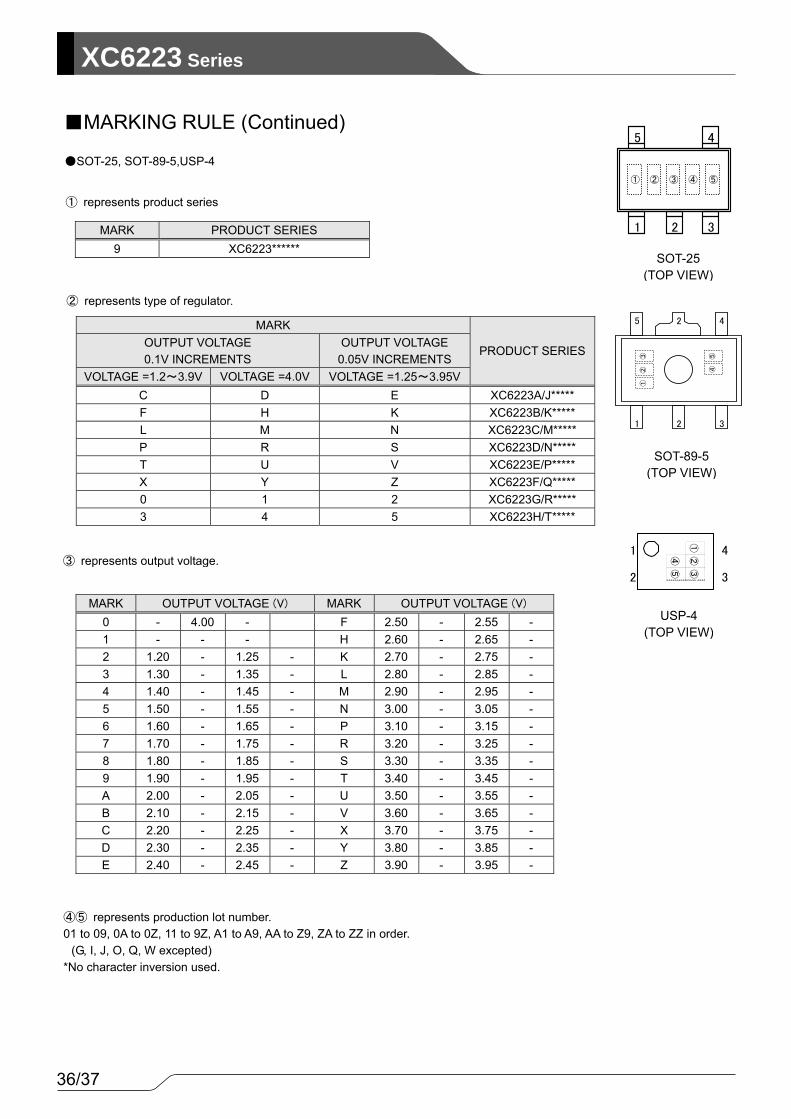
XC6223 Series SOT-25, SOT-89-5,USP-4
MARK PRODUCT SERIES
9 XC6223******
MARK
PRODUCT SERIES OUTPUT VOLTAGE 0.1V INCREMENTS
OUTPUT VOLTAGE 0.05V INCREMENTS
VOLTAGE =1.2~3.9V VOLTAGE =4.0V VOLTAGE =1.25~3.95VC D E XC6223A/J***** F H K XC6223B/K***** L M N XC6223C/M***** P R S XC6223D/N***** T U V XC6223E/P***** X Y Z XC6223F/Q***** 0 1 2 XC6223G/R***** 3 4 5 XC6223H/T*****
MARK OUTPUT VOLTAGE (V) MARK OUTPUT VOLTAGE (V)
0 - 4.00 - F 2.50 - 2.55 - 1 - - - H 2.60 - 2.65 - 2 1.20 - 1.25 - K 2.70 - 2.75 - 3 1.30 - 1.35 - L 2.80 - 2.85 - 4 1.40 - 1.45 - M 2.90 - 2.95 - 5 1.50 - 1.55 - N 3.00 - 3.05 - 6 1.60 - 1.65 - P 3.10 - 3.15 - 7 1.70 - 1.75 - R 3.20 - 3.25 - 8 1.80 - 1.85 - S 3.30 - 3.35 - 9 1.90 - 1.95 - T 3.40 - 3.45 - A 2.00 - 2.05 - U 3.50 - 3.55 - B 2.10 - 2.15 - V 3.60 - 3.65 - C 2.20 - 2.25 - X 3.70 - 3.75 - D 2.30 - 2.35 - Y 3.80 - 3.85 - E 2.40 - 2.45 - Z 3.90 - 3.95 -
① represents product series
② represents type of regulator.
④⑤ represents production lot number. 01 to 09, 0A to 0Z, 11 to 9Z, A1 to A9, AA to Z9, ZA to ZZ in order. (G, I, J, O, Q, W excepted) *No character inversion used.
SOT-25 (TOP VIEW)
1 2 3
5 4
① ② ③ ④ ⑤
③ represents output voltage.
MARKING RULE (Continued)
5 2 4
1 2 3
⑤③①
④②
SOT-89-5 (TOP VIEW)
③
1
2
4
3
①②④
⑤
USP-4 (TOP VIEW)

37/37
XC6223Series
1. The products and product specifications contained herein are subject to change without
notice to improve performance characteristics. Consult us, or our representatives
before use, to confirm that the information in this datasheet is up to date.
2. We assume no responsibility for any infringement of patents, patent rights, or other
rights arising from the use of any information and circuitry in this datasheet.
3. Please ensure suitable shipping controls (including fail-safe designs and aging
protection) are in force for equipment employing products listed in this datasheet.
4. The products in this datasheet are not developed, designed, or approved for use with
such equipment whose failure of malfunction can be reasonably expected to directly
endanger the life of, or cause significant injury to, the user.
(e.g. Atomic energy; aerospace; transport; combustion and associated safety
equipment thereof.)
5. Please use the products listed in this datasheet within the specified ranges.
Should you wish to use the products under conditions exceeding the specifications,
please consult us or our representatives.
6. We assume no responsibility for damage or loss due to abnormal use.
7. All rights reserved. No part of this datasheet may be copied or reproduced without the
prior permission of TOREX SEMICONDUCTOR LTD.