X-ray-induced changes in optical properties of doped and ...
117
X-ray-induced changes in optical properties of doped and undoped amorphous selenium A Thesis Submitted to the College of Graduate and Postdoctoral Studies In Partial Fulfillment of the Requirements for the Degree of Master of Science In the Division of Biomedical Engineering University of Saskatchewan By Yeon Hee Jung Saskatoon, Saskatchewan Copyright Yeon Hee Jung, January 2018.
Transcript of X-ray-induced changes in optical properties of doped and ...

X-ray-induced changes in optical properties of doped and undoped
amorphous selenium
A Thesis
Submitted to the College of Graduate and Postdoctoral Studies
In Partial Fulfillment of the Requirements for the Degree of
Master of Science
In the Division of Biomedical Engineering
University of Saskatchewan
By
Yeon Hee Jung
Saskatoon, Saskatchewan
Copyright Yeon Hee Jung, January 2018.

i
PERMISSION TO USE
In presenting this thesis in partial fulfillment of the requirements for a Postgraduate degree from
the University of Saskatchewan, I agree that the Libraries of this University may make it freely
available for inspection. I further agree that permission for copying of this thesis in any manner,
in while or in part, scholarly purpose may be granted by the professor or professors who
supervised my thesis work or, in their absence, by the Chair of the Department or the Dean of the
College in which my thesis work was done. It is understood that due recognition shall be given to
me and to the University of Saskatchewan in any scholarly use which may be made of any
material in my thesis.
Request for permission to Copy or to make other use of material in this thesis in whole or part
should be addressed to:
Chair of the Division of Biomedical Engineering
57 Campus Drive
University of Saskatchewan
Saskatoon, Saskatchewan, S7N 5A9
OR
Dean
College of Graduate and Postdoctoral Studies
University of Saskatchewan
116 Thorvaldson Building, 110 Science Place
Saskatoon, Saskatchewan, S7N 5C9

ii
ABSTRACT
Amorphous selenium has been used as an important material for the flat-panel X-ray image
detector. Its image quality is affected by a sensitivity which is reduced under high or long
duration of X-ray exposure due to the generation of defects. Experiments were conducted to
investigate the changes in optical properties of doped and undoped a-Se when the samples were
exposed to two doses of X-rays, 900 Gy and 3200 Gy, at 30 and 70 kVp. The samples were: a-
Se, a-Se:0.5% As, a-Se:6%As, a-Se:6% As and a-Se:6% As: ppm of Cs. After the cessation of
X-ray irradiation, the recovery of the optical properties towards pre-exposure equilibrium values
was also investigated. In addition, the dependence of optical properties on the temperature,
alloying and doping have been studied. The transmission spectra T(λ) of all films were scanned
from 450 nm to 2000 nm, and the thickness d, wedge Δ d, absorption coefficient α(λ), optical
band gaps EgT, EgU and refractive index n(λ) were extracted from Swanepoel method from T(λ).
The result shows that optical properties were influenced by the absorption of X-rays, heat and
doping. The change in n(λ) was related to densification by the Clausius-Mossotti equation. After
the cessation of X-rays, the n(λ) of the films relaxes back to the original state, after a certain
amount of time. The minimum time to relax to the equilibrium state after irradiation takes about
16 hours. The maximum changes in n(λ) and d were 0.27% and 0.27%. The changes in the
optical band gaps, EgT and EgU, were within experimental errors ±0.04%. Changes in the optical
constants induced by heating were measurably large. The changes in the optical constants by
alloying with As and doping with ppm amounts of Cs have been also studied. Alloying with As
increases n(λ) and decreases EgT, and further doping of Cs slightly increases n(λ).

iii
ACKNOWLEDGEMENTS
I would like to express appreciation towards my supervisor, Dr. S.O. Kasap, for his guidance,
advices, leadership, patience and support. Without him, it would have been impossible for me to
get into the right path for completing MSc. I also would like to thank Cyril Koughia, for his
advices, helps for analysis of thin film transmission data. I also would like to thank Dr. George
Belev, for sample preparation, for the excellent advices on experimental data, and for his
patience and his insights to all my questions. I also would like to thank Analogic Canada Corp
and University of Saskatchewan for financial support. I also would like to thank Farley Chicilo,
Thomas Meyer, Ozan Gunes, and Jun-Yi Yang for their help on dose calculations and
experimental set-up, on the experimental calculations, and instrumental problems. Finally, I
would like to thank God, my family for their encouragement and full support during MSc.

iv
TABLE OF CONTENTS
PERMISSION TO USE ................................................................................................................... i
ABSTRACT .................................................................................................................................... ii
ACKNOWLEDGEMENTS ........................................................................................................... iii
TABLE OF CONTENTS ............................................................................................................... iv
LIST OF FIGURES ...................................................................................................................... vii
LIST OF TABLES ....................................................................................................................... xiii
LIST OF ABBREVIATIONS ...................................................................................................... xvi
Chapter 1. Background ................................................................................................................... 1
1.1. Introduction ...................................................................................................................... 1
1.2. Digital Radiography ......................................................................................................... 3
1.3. Direct conversion flat-panel X-ray image detector .......................................................... 5
1.4. The X-ray photoconductor requirements ......................................................................... 7
1.5. Amorphous selenium as an X-ray photoconductor .......................................................... 8
Chapter 2. Properties of Amorphous Selenium ............................................................................ 10
2.1. Atomic structure of amorphous solids ........................................................................... 10
2.2. Band theory of amorphous solids ................................................................................... 11
2.3 Physical structure of amorphous selenium ..................................................................... 13
2.4. Density of states of amorphous selenium ....................................................................... 16
2.5 Optical properties of amorphous selenium..................................................................... 18
2.5.1 Optical Absorption ..................................................................................................... 18
2.5.2. Refractive index ......................................................................................................... 23
2.5.4 Dispersion ................................................................................................................... 25

v
2.5.5 Influence of polarization and density on the refractive index .................................. 29
2.5.6 Moss’s rule .............................................................................................................. 30
Chapter 3. Analysis of Thin Film Transmission spectrum ........................................................... 31
3.1 Introduction .................................................................................................................... 31
3.2 Principles of thin film optics .......................................................................................... 31
3.3. Swanepoel method ......................................................................................................... 34
3.4. Swanepoel’s uniform film technique ............................................................................. 37
3.4.2 Envelope construction ............................................................................................. 38
3.4.3 Determination of refractive index ........................................................................... 39
3.4.4 Substrate refractive index ....................................................................................... 40
3.4.5 Determination of thickness ..................................................................................... 41
3.4.6 Absorption coefficient ............................................................................................ 41
3.4.7. Swanepoel’s optimization method .......................................................................... 42
3.5 Swanepoel’s non-uniform film method.......................................................................... 48
3.5.1 Transmission of a non-uniform film ....................................................................... 48
3.5.2. Determination of wedge Δd in the transparent region ............................................ 49
3.5.3 Determination of refractive index n in medium absorption region......................... 50
3.5.4 Determination of thickness ..................................................................................... 51
3.5.6 Improvement in the extraction of optical constants ................................................ 53
3.6 Error analysis of all optical parameters .......................................................................... 55
Chapter 4. Experimental Procedure .............................................................................................. 56
4.2 Thin film deposition by thermal evaporation technique ................................................ 56
4.3 X-ray Faxitron chamber ................................................................................................. 59
4.4 Dose calculation ............................................................................................................. 60
4.5 Experimental air dose and dose measurement system ................................................... 63
4.6 Calculation of ideal dose in air and selenium ................................................................ 64
4.7 UV-VIS spectrophotometer............................................................................................ 69
Chapter 5. Results and Discussion ................................................................................................ 71
5.1 Optical properties of amorphous selenium influenced on heating ................................. 71
5.2 Influence of thickness on amorphous selenium ............................................................. 78

vi
5.3 Influence of alloying As and doping Cs on optical constants of a-Se............................ 80
5.4 X-ray induced effects ..................................................................................................... 84
5.5 X-ray relaxation effects .................................................................................................. 90
Chapter 6. Summary and Conclusion ........................................................................................... 93
References ..................................................................................................................................... 95

vii
LIST OF FIGURES
Figure 1.1. Schematic of radiography setup (from [13]). ............................................................ 3
Figure 1.2. A cross sectional view of two pixels with each of TFTs, storage capacitances Cij
and EHPs. The top electrode A is a vacuum coated metal and the bottom electrode
B is the pixel charge collection electrode. There is a thin dielectric layer between
the a-Se and the top electrode A and there is a doped a-Se alloy which is coated
between the pixel electrode B and a-Se photoconductor to reduce the injection of
electrons, and hence the dark current (from [3])....................................................... 5
Figure 1.3. A cross sectional view of thin film transistor (TFT) layer active matrix area
(AMA). The label “S” refers data (column) line, and the subscript “G” refers gate
(row) line (from [3])...................................................................................... ………6
Figure 1.4. The image of a hand from a direct-conversion flat-panel X-ray image detector
using a stabilized a-Se photoconductor (from [8]). .................................................. 9
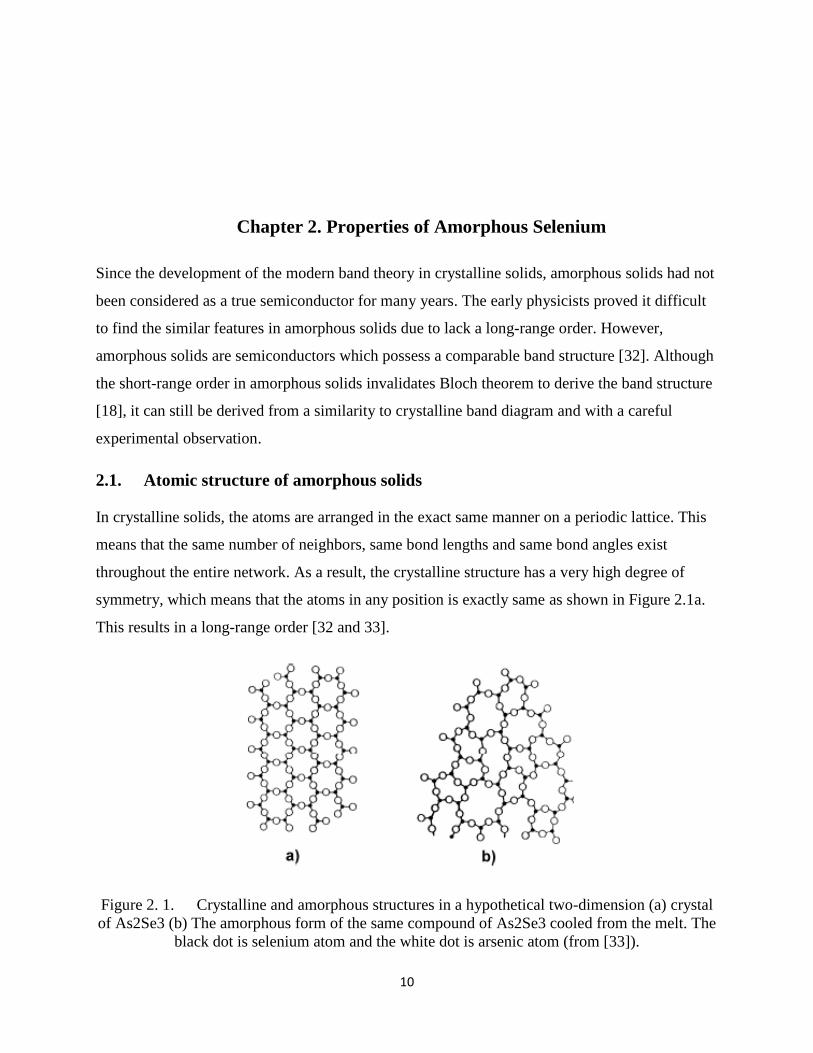
Figure 2. 1. Crystalline and amorphous structures in a hypothetical two-dimension (a) crystal
of As2Se3 (b) The amorphous form of the same compound of As2Se3 cooled
from the melt. The black dot is selenium atom and the white dot is arsenic atom
(from [33]). ........................................................................................................... 10
Figure 2. 2. The density of states of (a) a crystalline semiconductor (b) and (c) an amorphous
semiconductor. (b) Introducing fluctuations in the bond length and angle from
crystalline semiconductor (c) introducing chemical defects from (b) (from [36]).
12
Figure 2. 3. Random chain model of amorphous selenium (from [39]). ................................ 13
Figure 2. 4. The structure and p-level energy of bonding configurations for selenium atom (C
14 refers to Se). Straight line represents bonding orbitals, a lobe represents a lone-
pair orbital, and a circle represents an anti-bonding orbital. The energy level
consists of the three states from the top: σ∗, lone-pair electron, and σ states.
Energies are given as zero for LP energy (from [40]). ………………………….14
Figure 2. 5. Schematic diagram of VAP and IVAP (from [43])............................................. 15
Figure 2. 6. The original DOS distribution of a-Se based on Abkowitz (from Abkowitz [44]).
16
Figure 2. 7. The DOS distribution of a-Se based on reference (from [42]). ........................... 17
Figure 2. 8. The optical transitions in amorphous semiconductor (after [49]). ...................... 19

viii
Figure 2. 9. (a) The optical absorption coefficient as function of photon energy for typical
amorphous semiconductor (after [43]) and (b) The optical absorption
characteristics for a-Se (after [21]). ...................................................................... 19
Figure 2. 10. Tempreature dependence on (a) Tauc band gap EgT and (b) Urbach energy Egu
for amorphous selenium (after Ticky [55]). .......................................................... 21
Figure 2. 11. Temperature dependence on Tauc band-gap Eg and Urbach energy Eu for As2Se3
(after [54]). ............................................................................................................ 22
Figure 2. 12. Absorption spectra of As2S3 in a bulk sample (open circle) and as-evaporated
film (solid circle) with weak absorption tails of different Fe concentration (pure,
26 ppm, 120 ppm and 220 ppm) (after Tanaka [56]). ........................................... 23
Figure 2. 13. (a) Complex relative permittivity of a silicon crystal as a function of photon
energy plotted in terms of the real and imaginary parts. (b) The optical properties
of a silicon crystal vs. photon energy in terms of the real (n) and imaginary (K)
parts of the complex refractive index (After [51]). ............................................... 26
Figure 2. 14. The refractive index of pure amorphous selenium film with d ̅ = 1756nm and Δd =
11nm fitted into Cauchy (blue line) and Sellmeier (dotted green line) dispersion
equations. .............................................................................................................. 28
Figure 3. 1. Light travelling in a medium of refractive index n1 is incident on a thin film of
index n2 (after [63]). .............................................................................................. 32
Figure 3. 2. (a): Light transmitting through an absorbing thin film (uniform thickness) on a
thick finite transparent substrate [46]. (b): Transmission spectra of pure a-Se
uniform film of d= 1.816µm (full curve) compared to that of simulated
transmission when assuming no absorption (dotted curvy) with substrate (linear
line). ...................................................................................................................... 34
Figure 3. 3. (a): Light transmitting through an absorbing thin film with a variation in thickness
(non-uniform) on a thick finite transparent substrate [47]. (b): Simulated
transmission of pure a-Se film with uniform thickness of 1.816µm (dotted-curve
spectrum) and transmission of the same pure a-Se film with a roughness Δd = 30
nm (full-curve spectrum). ..................................................................................... 36
Figure 3. 4. The construction of lower and upper envelopes in the transmission spectra for a
1.816µm uniform film of a-Se. The red dashed curve is an upper envelope and
blue dashed curve a lower envelope. .................................................................... 38
Figure 3. 5. Improvement on refractive index of pure a-Se uniform film. The crude n was
obtained from equation (3.9), and n2 was obtained from improving thickness
using equation (3.16c), which is a poor approximation in strong absorption, and
nfit is the best dispersion curve (3.16d) without any deviations........................... 40

ix
Figure 3. 6. Re-generated transmission spectrum from average thickness d ̅new of 1816.5 nm
with Sellmeier coefficient terms (A = 4.32, B = 1.67 and C = 467nm), according
to Table 3.2. .......................................................................................................... 47
Figure 3. 7. The spectral dependence of the refractive index of pure a-Se non-uniform film.
The nfit value is obtained from the fit of the Sellmeier dispersion with coefficients
(A = 4.49, B = 1.63 and C = 472 nm) of nmeasured. (The n1 and n2 are from
equations (3.21) and (3.22) respectively) ............................................................. 51
Figure 3. 8. Re-generated transmission spectra of a pure a-Se non-uniform film obtained from
𝑑2= 1755.8 nm and d = 10.7 nm according to Table 3.3. ................................ 53
Figure 4. 1. Typical boat and substrate temperature vs. time profile. During the deposition,
boat and substrate temperature are constantly controlled and monitored (after
[25])....................................................................................................................... 57
Figure 4. 2. A schematic of the evaporation assembly inside the vacuum chamber (after [43]).
58
Figure 4. 3. Faxitron Cabinet X-ray system (after [66]). ........................................................ 59
Figure 4. 4. Keithley 35050 dosimeter (left) and the air-filled detection device, the Keithley
ion chamber (right) (after [66]). ............................................................................ 63
Figure 4. 5. The simulated X-ray spectrum of fluence at 30 kVp and 70 kVp (from Siemens
[68])....................................................................................................................... 65
Figure 4. 6. Mass Attenuation coefficients µ/ρ (black) and mass energy absorption coefficients
µen/ρ (red) of air (left) and Se (right). The data point is obtained from NIST [70],
and linear curve data was obtained by taking logarithmic interpolation both in
photon energy and in mass coefficients (after [70]). ............................................ 66
Figure 4. 7. Energy spectrum of theoretical dose of air (black) and pure a-Se (red) at 30 kVp
from Table 4.4 (The inset of the figure is expanded to show the dose of air). ..... 68
Figure 4. 8. Energy spectrum of absorbed dose in 20 minutes for pure a-Se with its thickness
68
Figure 4. 9. A schematic diagram of the spectrophotometer assembly (after [71]). .............. 69
Figure 4. 10. The workstation for UV-Visible spectrophotometer (after [72]). ....................... 70
Figure 5. 1. The transmission spectra of pure a-Se film at room temperature and at 328 K (55
C). ........................................................................................................................ 72
Figure 5. 2. Sellmeier refractive index dispersion for an a-Se film after heating. The solid line
represents the dispersion at room temperature and dotted line is the dispersion
after heating at 328K. ............................................................................................ 74
Figure 5. 3. The normalized changes in thickness (d/do) (black curve) and refractive index
(Δn/no) (red curve) as a function of compositions in a-Se: pure a-Se, a-Se 0.3%

x
As, a-Se 6% As, a-Se 6% As + 220ppm Cs after heating to glass transition
temperature Tg. The shaded area corresponds to statistical errors in Δd/d and Δn/n
determination and is based on assigning 2σ to the full width of error region. ..... 74
Figure 5. 4. Absorption coefficient of a pure a-Se film at room temperature (RT) and after
heating at 328K for the determination of Urbach band-gap EgU in the low
absorption region (α < 104 cm-1). .......................................................................... 77
Figure 5. 5. Absorption coefficient of a pure a-Se at room temperature and after heating at
328K for the determination of Tauc band-gap EgT in the high absorption region (α
> 104 cm-1). ........................................................................................................... 77
Figure 5. 6. The determination of EgT in α > 104 cm-1 for two different thickness films of a-
Se:6%As. ............................................................................................................... 79
Figure 5. 7. The determination of EgU in α < 104 cm-1 for two different thickness films of a-
Se:6%As. ............................................................................................................... 79
Figure 5. 8. The refractive index dispersion diagram for the various composition a-Se films ..
82
Figure 5. 9. The optical absorption coefficient (αhυ) vs photon energy (hυ) of the different
composition a-Se films for the determination of EgT in α > 104 cm-1. .................. 82
Figure 5. 10. The optical absorption coefficient (α) vs photon energy (hυ) of the different
composition a-Se films for the determination of EgU in α < 104 cm-1. .................. 83
Figure 5. 11. Refractive index vs. wavelength for a-Se:6% As film (red curve) and a-Se:6% As
+140ppm Cs doped films (blue curve) before (black curve) and after irradiation at
70 kVp. .................................................................................................................. 86
Figure 5. 12. The relative change of refractive index Δn/no, triangle symbols, and thickness
Δd/do, square symbols as a function of compositions in a-Se: pure a-Se, a-Se 0.5%
As, a-Se 6% As, a-Se 6% As + 140ppm Cs after irradiating at 30 kVp (red line)
and 70 kVp (blue line). The shaded area corresponds to statistical errors in Δd/d
and Δn/n determination and is based on assigning 2σ to the full width of error
region. ................................................................................................................... 86
Figure 5. 13. The relative change of thickness (Δd/d), square symbols, and refractive index
(Δn/n), triangle symbols, in a-Se samples with varying compositions (dotted
curves) as a function of delivered (absorbed) dose in a-Se. a-Se, black; a-Se 0.5%,
red; a-Se 6% As, green; a-Se 6% As +140 ppm Cs, purple; after irradiation with
30 kVp (900 Gy) and 70 kVp (3150 Gy). Shaded area corresponds to statistical
errors in Δd/d and Δn/n determination and is based on assigning 2σ to the full
width of error region. ............................................................................................ 87
Figure 5. 14 The 70kVp irradiation and time evolution of the thickness Δd/do and refractive
index Δn/no, during and after X-ray irradiation, where do and no are the initial
thickness and refractive index of a-Se:6% As virgin film. The 70kVp label refers

xi
to the end of irradiation (The error bars represent maximum possible error in
here). ..................................................................................................................... 91

xii
LIST OF TABLES
Table 1. 1. Selected properties of stabilized a-Se for the x-ray layers for use as X-ray
photoconductors (from [17]). .................................................................................... 9
Table 3. 1. Optical parameters of pure a-Se uniform film obtained from 𝑑new of 1810.9nm.
Values of λext, s, TM and Tm for the spectrum of figure 3.6. Calculation of N, ncrude,
nnew, nfit and dcrude and dnew. (N from equation (3.9a), ncrude from equation (3.9).
dcrude from equation (3.12). mcrude and m from equation (3.16a). dnew from equation
(3.16b). nnew from equation (3.16c). nfit from equation (3.16d) with Sellmeier
coefficient terms: A 4.35, B 1.68 and C 467nm). .......................................... 45
Table 3. 2. Improvements of thickness (𝑑new) and optical constants (nnew and nfit) of pure a-Se
uniform film with reduced RMSE (0.466%) using re-iteration method in Matlab.
Thickness (𝑑new) is 1816.2 nm and the Sellmeier coefficient terms of nfit is: A
4.32, B 1.67 and C 467nm. ............................................................................... 46
Table 3. 3. Optical parameters of non-uniform pure a-Se film, obtained from d of 1755.8nm
with d = 10.7 with 0.64% RMSE, and Values of λext, s, TM and Tm are for the
spectrum of figure 3.8. Calculation of n1, Δd and n2, x and d1, d2 and n3, nfit. (n1 and
Δd from equation (3.21), n2 and x from equation (3.22). d1 from equation (3.12).
mcrude and m from equation (3.16a). d2 from equation (3.16b). n3 from equation
(3.16c). nfit from equation (3.16d)). Sellmeier coefficient terms for nfit is: A = 4.49,
B = 1.62 and C = 472 nm. ....................................................................................... 54
Table 3. 4. Analysis of a-Se alloyed with 0.5% As film in terms thickness d, refractive index n
and two optical band gaps EgT and EgU, using nine different measurements on
different spots on the film surface. ......................................................................... 55
Table 4. 1. Typical fabrication conditions for the thermal deposition of a-Se (pure/0.5% As/6%
As/6% As + Cs) films during the deposition, which was used for X-ray irradiation
experiments. P is chamber pressure, Tb is the boat temperature, tevap is the time
duration of deposition, Ts is the substrate temperature and d is the thickness of
film. ......................................................................................................................... 58

xiii
Table 4. 2. Absorbed dose in 20 minutes for listed samples which were placed at shelf No.8
(303cm) in the X-ray chamber, using total incident dose 15.93 Gy of air at 30 kVp
in 20 minutes. .......................................................................................................... 63
Table 4. 3. The incident dose rate in air at 70 kVp by using a correction factor 34.36 (The
correction factor was found by dividing bare rate of 98.28 V/m from filtered rate of
2.86 V/m at shelf number of two). .......................................................................... 64
Table 4. 4. Theoretical deposited dose of air and pure a-Se (thickness 1756nm) at photon
energy (keV). Values of en and Φ(E) are from the spectrum of figure 4.5
and 4.6. Calculation of Eabsorbed and Eabsorbed/M of air and Se (Eabsorbed/M of air from
equation (4.4a), and Eabsorbed/M of Se from equation (4.5a) in unit of Gray). ......... 67
Table 5. 1 The influence of the heating at Tg on optical properties for different composition a-
Se films: pure a-Se, a-Se: 0.3% As, a-Se: 6% As and a-Se: 6% As: 220ppm Cs (RT
refers a sample well-aged and relaxed at room temperature). (Note that Tg is 49°C
for pure a-Se, 85°C for a-Se:6% As, and 75°C for a-Se:6% As + 220ppm Cs). .... 72
Table 5. 2 The optical parameters of curve fitting n to the Wemple-DiDominicio relationship
(nWD is the Wemple-DiDominicio refractive index at 2000nm). ............................. 75
Table 5. 3 Fitting parameters of two optical band gaps of films at RT and Tg. The Tauc band
gap: αhυ = A(hυ-EgT) and Urbach gap: α = C×exp(hυ/ΔE), where A = Tauc
constant, EgT = Tauc band-gap, α refers to the absorption coefficient (cm-1), EgU =
Urbach band-gap and ΔE refers to Urbach energy. RT refers to a film kept at room
temperature (aged) just before heating. .................................................................. 76
Table 5. 4. The influence of thickness on optical properties for the a-Se:0.5%As film
(thickness difference between the two ~0.4 µm) and a-Se:6% As film (thickness
difference ~0.3 µm). ............................................................................................... 78
Table 5. 5. Optical properties of a-Se when alloying As and doping Cs on a-Se with different
concentrations. ........................................................................................................ 80
Table 5. 6 Optical properties of the four components of a-Se films (pure a-Se, a-Se:0.5% As,
a-Se: 6% As, a-Se: 6% As 140ppm Cs) before and after X-ray irradiation at 30 and
70 kVp. .................................................................................................................... 85
Table 5. 7. Optical band gaps and its fitting parameters of the X-ray irradiation..................... 88
Table 5. 8. Wemple Di-Dominicio model parameters of X-ray irradiation. ............................. 89
Table 5. 9. Optical properties of X-ray reversibility of a-Se:6% As ........................................ 90
Table 5. 10. Wemple Di-Dominicio coefficients of X-ray relaxation. .................................... 92
Table 6. 1. Summary of optical properties for a-Se films. ....................................................... 94

xiv
LIST OF ABBREVIATIONS
a-Se amorphous selenium
AMA active matrix arrays
FPD flat panel detector
TFTs thin film transistors
EHPs electron-hole pairs
SFR screen and film radiography
DOS density of states
VAP valence alternate pairs
IVAP intimate valence alternate pairs
TOF time of flight
NIR near infrared
UV ultraviolet
PPM parts per million
NB non-bonding
LP lone pair
RMSE Root mean square error

1
Chapter 1. Background
1.1. Introduction
Since Roentgen’s discovery of X-rays in 1895, the X-ray imaging has been used as a medical
diagnosis tool to image human body structures. There have been many scientific refinements in
equipment and techniques in X-ray imaging over the years. Especially, the development of
computers and filmless radiology introduced digital radiography in 1980s [1] where X-ray
images are generated from a detector and directly recorded on a computer [2 and 3].
Digital radiography has evolved into different forms and one of the most recent and promising
developments is the direct conversion flat-panel X-ray image detector (FPD) [3]. The direct
conversion FPD is made by coating an X-ray photoconductor on top of a large area integrated
circuit called an active-matrix-array (AMA). The AMA consist of millions of small pixels, each
of which acts as a small detector to capture X-rays and convert them to charge directly [4]. The
technology based on active-matrix flat-panels enables an efficient and effective method to
generate an image. The FPD is the only detector today meeting a lot of requirements, such as
active area, pixel size, image acquisition rate, and dynamic range for covering various
applications, including general radiography, mammography, angiography and fluoroscopy [5].
The direct conversion FPD not only meets all the basic requirements for clinical use, such as
cost, instant availability of the image, reduced dose, high sensitivity of X-rays [3], but also
provides the highest image quality [2]. However, there are many unsolved problems and the one
of problems is the lack of any information on damaging a-Se layers upon X-ray exposure.
Ideally, a detector should not experience any changes in the material properties upon X-ray
exposure [3]. Otherwise, its image resolution as well as image characteristics can be significantly
affected. For instance, it is known that a high dose of X-rays decreases the X-ray sensitivity of

2
the photodetector, leading to a ghost of the previous image [6 and 7].
Therefore, we decided to study the X-ray induced optical properties of n-like a-Se layer in an a-
Se detector. The current direct conversion FPD has used stabilized a-Se (0.2-0.5% As and doped
with 0-20 ppm Chlorine) as an X-ray photoconductor [8]. The samples used in this study were:
(a) pure a-Se, (b) a-Se: 0.5% As (c) a-Se: 6% As and (d) a-Se: 6% As doped with the 140 – 220
ppm of Cs. The photo-induced effects in a-Se has other applications in optoelectronic and
photonic devices such as a grating and photoresist [24, 86].
Our research investigates the optical properties of doped and undoped a-Se under low and high
doses of X-rays. We first studied if optical properties are influenced by other external stimuli or
factors such as heat, thickness and doping. Then, we examined changes in optical properties for
the different doping compositions of a-Se with low and high doses of X-rays. Finally, we
examined changes in optical properties over time after completing X-ray irradiation to see if the
properties relaxed to their original states. The objective of this research was to see if X-ray
irradiation gives clear changes in the optical properties of a-Se.
A previous study showed that defects are generated during X-ray irradiation and these induced
defects are annealed out over time [7]. So, we also tried to identify the X-ray induced defects
upon X-ray irradiation and examined the changes over time after irradiation to see if x-ray
effects are permanent or temporary. The optical properties of interests were the refractive index
n, thickness d and two optical band gaps EgT and EgU.

3
1.2. Digital Radiography
In general, projection imaging is employed as a common X-ray imaging technique to obtain an
image. This technique is based on projecting a shadow image of internal structures of the objects
onto the detector [9]. In projection radiography, the procedure to obtain an image is divided into
three steps: X-ray generation, attenuation of the beam and image creation, which is shown in
Figure 1.1 below.
First, the special generator supplies a high-power voltage into an X-ray tube; the electrons flow
from cathode to anode (i.e. tungsten target) inside the X-ray tube. The high energy electron
undergoes an energy loss, which results in generating X-ray energy [10].
As X-rays pass through the patient, the variation in thickness, density or atomic composition of
the different tissues causes variations in the transmission and absorption of the X-rays [11]. The
dense tissues such as a bone absorbs most of X-ray beam and the soft tissues allow X-rays to
penetrate relatively easier. The transmitted X-ray beams are captured by a detector and the
absorbed X-rays are not captured [12]. The difference in penetration between two different
mediums (i.e. two tissues) determines the X-ray contrast in the final X-ray image [9].
Figure 1.1. Schematic of radiography setup (from [13]).

4
The traditional method to obtain an X-ray image is to use a film in a close contact with a light-
emitting screen. This method, so called screen and film radiography (SFR), suffers from a lot of
disadvantages such as limited storage, high cost of film, film distribution, image processing, and
high dose of X-rays (Fixed dose latitude). The image process in SFR is time-consuming and uses
a chemical for the image development [1,2,3].
The digital radiography has replaced a lot of the disadvantages of SFR over the last thirty years
[14]. First, the digital images can be expanded and shrunk in the greater details and manipulated
without destroying the original, whereas in the SFR system, the images become permanent in the
film once it has been processed. The manipulation of images is the great advantage for
physicians who need to examine the structure and change the structure from normal to abnormal
[16]. Secondly, the images are now stored in an electronic medium. This means that there is no
risk of losing images and images are available at anywhere and anytime. Thirdly, it increases a
dose efficiency from a larger dynamic range, which enables to reduce a high exposure to the
patient [1,2].
One of the most successful developments was the FPD introduced in the end of the 1990s. The
FPD integrates an electronic read out system based on AMA with an X-ray detection material
(i.e. a photoconductor or phosphor) [14, 15]. This active matrix readout provides efficient and
instant means to detect, store and measure the electrical charges [15]. By combining this readout
with an X-ray detection material, the FPD is capable for capturing the X-ray image immediately
after the exposure [3]. Its system eliminates the image creation step, the image plate reader step
or the image development in the dark room, since the read out is essentially self-scanning in that
no external means are required [1,3].
The FPD provides the highest spatial resolution with the best image quality and the fastest
readout than with any other X-ray devices [2, 5]. The time lapse on displaying images after X-
ray exposure is less than 10 seconds, allowing more patients to be examined in the same amount
of time than with other radiographic devices [5]. The image generation is a real-time process [2].

5
1.3. Direct conversion flat-panel X-ray image detector
There are two types of flat-panel X-ray detectors depending on detection (conversion) types. The
direct conversion uses an X-ray photoconductor (i.e. a-Se) which converts X-ray photons directly
into electrical charges. The indirect conversion uses a scintillator (i.e. CsI) to convert X-rays into
visible light, which in turn is converted into an electrical charge by means of an a-Si photodiode
arrays [14]. Both the direct conversion and indirect conversion detectors incorporate the active
matrix readout (AMA) in which each pixel element contains a sensing and storage element, a
switching element (photodiode and TFT), and image processing module to detect, store and read
the charges [15].
Figure 1.2 below shows a cross-sectional structure of two pixels (i, j) and (i, j+1) with TFTs for
the direct-conversion flat-panel X-ray imager. Each pixel element in the AMA acts as an
individual detector to detect X-rays and convert it to an amount of charge ΔQ proportional to the
amount of incident X-rays. These charges are carried by a corresponding pixel capacitor Cij at (i,
j) to store and then read out, when the TFT switches are on. The external electronics control the
state (on and off) of TFTs switches [3, 4, 8].
Figure 1.2. A cross sectional view of two pixels with each of TFTs, storage capacitances Cij
and EHPs. The top electrode A is a vacuum coated metal and the bottom electrode B is the pixel
charge collection electrode. There is a thin dielectric layer between the a-Se and the top electrode
A and there is a doped a-Se alloy which is coated between the pixel electrode B and a-Se
photoconductor to reduce the injection of electrons, and hence the dark current (from [3]).

6
The charges can be read by properly coordinating the gate line i and data line j of the TFT (i, j).
The gates of all the TFTs in each row i and data of all TFTs in each column j are connected by
the same gate line i and same data line j, each respectively as shown in Figure 1.3. The read-out
is started when the TFT is switched on via the gate line i [5]. When gate line i is activated, then
N data lines from the first column j = 1 to the last column j = N read the charges on the pixel
electrode in row i. The charges are read out row by row, multiplexing the parallel columns to a
series of digital signal and then sent into a computer for image. Then, the next row, next gate line
i + 1, is activated and the same N data lines read the charges in row i +1. The whole steps are
repeated until the whole matrix has been read from the first row i = 1 to the last row i = N. This
mechanism is based on self- scanning [3].
Figure 1.3. A cross sectional view of thin film transistor (TFT) layer active matrix area
(AMA). The label “S” refers data (column) line, and the subscript “G” refers gate (row) line
(from [3]).

7
1.4. The X-ray photoconductor requirements
The selection of the photoconductive material in the detector is critical because it greatly affects
the detector performance [17]. The most important factor for X-ray photoconductors is the X-ray
sensitivity. The X-ray sensitivity, which is the amount of charges collected from absorbing
radiation, is controlled by three major quantities: i) the X-ray absorption, which relies on the
attenuated fraction of photons ηQ [1exp (αL)], with a linear attenuation coefficient α with the
large thickness L of the photoconductor, ii) the number of charge carrier generation, which relies
on the amount of photo-generated charges ΔQ = eΔE/W± from the absorbed radiation of energy
ΔE with W± is ionization energy of EHPs and, iii) a collection efficiency of the charge carriers [3,
4 and 5]. Above all, the ideal photoconductor should have the following material properties,
a. The photoconductor should have high intrinsic X-ray sensitivity. That means that it
should have high X-ray absorption with a high absorption coefficient α with the large
thickness L of the photoconductor. Furthermore, the penetration depth 1/α should be less
than the thickness L, that is 1/α << L. It is because all incident X-ray radiation should be
absorbed within the thickness of a detector to avoid the unnecessary exposure to patients.
b. There should be no deep trapping of EHPs, which means that the charge carrier
schubweg, the distance a carrier drifts before it is trapped and becomes unavailable, µF,
should be greater than the thickness of detector L, that is L<<µF. where µ is a drift
mobility, is deep trapping time and F is electric field.
c. There should be no recombination of electrons and holes.
d. The photoconductor should be coated onto the AMA panel easily (i.e. conventional
vacuum deposition) over large area with uniform quality [18]. The detector needs to be
larger than the body part to be imaged.
e. All the properties (a-e) above should not change with time or due to repeated and long x-
ray exposure [8].
Although a high quantum efficiency requires the large thickness of the detector, the detector
thickness L is limited to schubweg and X-ray penetration depth, that is, 1/α << L<< µF
from factor a and b.

8
1.5. Amorphous selenium as an X-ray photoconductor
The ideal candidate should satisfy all the requirements from a tog, and there are PbI2, PbO,
CdTe and HgI2 with good absorption characteristics. However, these involve the small areas
which are not suitable as an X-ray photoconductor [5, 18]. The a-Se seems the best candidate
since it i) is easily deposited into active matrix area readout circuit and is coated over large areas
(i.e. 40 cm × 40 cm or larger), ii) has an acceptable x-ray absorption coefficient, iii) it has good
charge transport properties for both holes and electrons, iv) has low dark current [3] and v) has a
high intrinsic spatial resolution [14].
a-Se has the inherent ability to generate charge carriers under exposure [19]. It was Willoughby
Smith, who discovered the photoconductivity ability of selenium by testing a resistance of sub-
marine telegraphic cables under light [8]. Since then, it has been used as a photocell, solar cell
and electrical rectifier [19]. The amorphous form of selenium was used in xeroradiographic
photoreceptor, then it has been replaced by FPD by replacing its toner with electronic readout
[8].
The stabilized amorphous selenium (a-Se alloyed 0.3-0.5% As and doped with the ppm level of
chlorine) is currently used as direct conversion FPD. The pure amorphous selenium crystallizes
over time, which results in a higher dark conductivity. Hence, a small portion of As is added in
a-Se to retard the crystallization rate and to increase viscosity. The As atoms (valency of three)
in the structure are triply bonded [20], and linked to three free chain ends, which lead to a
decrease in the number of free chain ends [21]. However, a high concentration of As introduces
deep hole traps and shortens the hole range, which result in reducing the photoconductivity of a-
Se. This can be compensated by doping halogen (i.e. Cl), which restores loss of hole transport
[20]. Table 1.1 summarizes all important properties of the stabilized a-Se and Figure 1.4 shows
the image of a hand generated by using a stabilized a-Se photoconductor.

9
Table 1. 1. Selected properties of stabilized a-Se for the x-ray layers for use as X-ray
photoconductors (from [17]).
Figure 1.4. The image of a hand from a direct-conversion flat-panel X-ray image detector
using a stabilized a-Se photoconductor (from [8]).
10
Chapter 2. Properties of Amorphous Selenium
Since the development of the modern band theory in crystalline solids, amorphous solids had not
been considered as a true semiconductor for many years. The early physicists proved it difficult
to find the similar features in amorphous solids due to lack a long-range order. However,
amorphous solids are semiconductors which possess a comparable band structure [32]. Although
the short-range order in amorphous solids invalidates Bloch theorem to derive the band structure
[18], it can still be derived from a similarity to crystalline band diagram and with a careful
experimental observation.
2.1. Atomic structure of amorphous solids
In crystalline solids, the atoms are arranged in the exact same manner on a periodic lattice. This
means that the same number of neighbors, same bond lengths and same bond angles exist
throughout the entire network. As a result, the crystalline structure has a very high degree of
symmetry, which means that the atoms in any position is exactly same as shown in Figure 2.1a.
This results in a long-range order [32 and 33].
Figure 2. 1. Crystalline and amorphous structures in a hypothetical two-dimension (a) crystal
of As2Se3 (b) The amorphous form of the same compound of As2Se3 cooled from the melt. The
black dot is selenium atom and the white dot is arsenic atom (from [33]).

11
In amorphous solids, however, atoms are arranged in a broken symmetry and periodicity. Figure
2.1 (b) shows a schematic diagram of amorphous form of the As2Se3, formed by quenching from
the liquid. Since the structure is not equivalent, the energy required to break and form the bond
in an atom is distinct to each other. There are also variations in bond angles from atom to atom,
which result in loss of periodicity and hence, losing a long-range order. This arrangement is
known as a short-range order. The important point is that the presence and absence of periodicity
and symmetry distinguish crystalline solids from amorphous solids [32 and 33].
2.2. Band theory of amorphous solids
When the atoms are brought together to form a solid, the atomic energy level is split into finely
separated molecular energy levels to form a continuum, an energy band. The band theory derives
these energy bands with an available energy level by applying the allowed quantum
mechanical wave functions for an electron in a solid, and the density of states (DOS) g (E) is
used to express the number of states available per unit energy per unit volume.
In a crystalline solid, the periodic atomic arrangement results in periodic potential energy of
electrons. Solving for the Schrondinger equation with the periodicity of potential energy leads to
the Bloch wave and the allowed energy levels. These energies are arranged in conduction or
valence bands. There are also energy ranges for which there are no Bloch wavefunctions, and
hence no allowed energies from valence band to conduction band, a band gap [32]. As a result,
there are well-defined conduction and valence bands which are separated by an energy gap in a
crystalline solid, as shown in Figure 2.2. Between a band and a band gap, there is a sharp band
edge where the DOS drops to near zero [34].
In an amorphous solid, the loss of translational periodicity does not allow to use the Bloch
theorem. However, an amorphous solid still possesses an energy band with a mobility gap, and it
turns out that electronic properties are similar from crystalline properties, since the band
structure is generally determined by a short-range order [35]. Nevertheless, amorphous solids
have slight variations in its DOS diagram resulting from the loss of the periodicity of the
equivalent crystalline structure, which is shown in Figure 2.2b and 2.2c.

12
Figure 2. 2. The density of states of (a) a crystalline semiconductor (b) and (c) an amorphous
semiconductor. (b) Introducing fluctuations in the bond length and angle from crystalline
semiconductor (c) introducing chemical defects from (b) (from [36]).
First, the sharp band edges in a crystalline solid in figure 2.2a become smeared or broadened.
This broadened state begins at the band edges Ecc and Ecv and extends into the forbidden gap in
figure 2.2b. The wavefunction between valence band edge Ecv and conduction band edge Ecc
forms localized states where its probability of finding the electron is “localized” at certain spatial
locations. Since its electrons are trapped or confined in this localized region, this state is also
known as a trap or tail state. This state arises from the deviations in bond angles and bond
lengths [32, 34 and 35].
Secondly, the traps in the localized states in Figure 2.2c are attributed to the specific defects of
the amorphous semiconductors [21]. These are coordination defects (valence alternate pairs),
dangling bonds or dopants [32].
In addition, there is a band edge, which separates extended states from localized states, known as
a mobility edge, which is Ecc and Ecv in Figure 2.2b and 2.2c. The name mobility edge derives
from the change in the mobility of charge carriers across Ecc or Ecv. The electrons are mobile at
zero temperature in the extended states and immobile within the localized states at zero degree.
The region of zero mobility leads to the concept of the mobility gap, which is energy from
valence band Ecv to conduction band mobility edges Ecc, which can be considered as a band gap
in amorphous solids [14, 32].

13
2.3 Physical structure of amorphous selenium
Crystalline selenium has two types of allotropes: α-monoclinic Se (α-Se) and trigonal Se (γ-Se).
In trigonal Se, all phases of dihedral angle are either positive (++++) or negative (---), promoting
to a local helicity, whereas the phases are alternating (+-+-+-+-+-) in α-monoclinic Se,
promoting to a ring-like structure [38]. The dihedral angle is defined as the angle between the
adjacent bonding planes [41].
The amorphous structure of selenium follows a random chain model, in which the two-fold
coordinated atoms have the same magnitude of dihedral angle, with changing its sign in random.
A random variation in phase means that a-Se consists of disordered mixture of chain fragments
from γSe chains and ring fragments from αSe rings [37]. The phase of a-Se in Figure 2.3 is
expressed by , where the front +++ and the back --- regions are chain
segments which possess a helical character, and the middle -+-+ region is the ring segment. This
is a chain-like structure which loses a regular helical character, and it can bend, twist, turn, or
“meander” through it [38]. The evidence for the alternation of dihedral angle in phase with the
ring- and chain-fragments was already proven from Raman scattering [39].
Figure 2. 3. Random chain model of amorphous selenium (from [39]).
There are potentially six types of bonding configurations in selenium. The Se20 configuration is
the lowest, most stable energy configuration, which is involved in normal bonding. There are

14
also a pair of charged defects, known as valence alternation pairs, which are a negatively charged
selenium atom with a single valence, Se1-, and a positively charged selenium atom with a triple
valence, Se3+. These defects, Se3
+ and Se1-, are intrinsic defects in thermal equilibrium, free-
energy derived equilibrium [21], since the formation energies of a VAP (Se3+ + Se1
-) and the
atom in the Se20 state are estimated to be -4Eb +ULP and -2Eb, respectively, according to Kastner
model [40]. This means that the VAP is more stable state than the Se20 state, hence favourable to
form. The concentration of VAP was found out to be 1016 cm-3 in Electron spin resonance
measurement [40].
If the atom in the Se1- and Se3
+ states retains one hole and one electron respectively, then these
form the neutral, excited Se10 and Se3
0 states. These Se30 and Se1
0 states are in non-equilibrium
that return to the original Se3+ and Se1
- states by releasing retained charged carriers, which are
unstable [21]. In Figure 2.4 below, the formation energies of Se30 and Se1
0 are -2Eb +Δ and -Eb,
respectively, which both are higher than that of the Se20 state, -2Eb, hence more unstable.
Figure 2. 4. The structure and p-level energy of bonding configurations for selenium atom (C
refers to Se). Straight line represents bonding orbitals, a lobe represents a lone-pair orbital, and a
circle represents an anti-bonding orbital. The energy level consists of the three states from the
top: σ∗, lone-pair electron, and σ states. Energies are given as zero for LP energy (from [40]).

15
The Se20 has 4s2 4p4 valence electron configurations with two valence electrons in s-state and
four electrons in p-state. The two electrons in p-state form two covalent bonding orbitals with
neighbor atoms and the four remaining electrons in s- and p-states form two lone-pairs orbitals.
The bonding orbitals form strong covalent bonds, whereas the two lone pair orbitals are
electronically attracted to the cores of atoms in neighbors, forming van der Waals bonds [41].
The van der Waals bonds interact with neighbor atoms of the solid through lone pair electrons,
holding the Se chains in a solid. The van der Waals play an important role in stabilizing the chain
structure.
In the amorphous structure, the lone pairs of atoms are disoriented which is enough to cause
tension between chains. The tension is so strong that it destabilizes the interactions between
chains. To reduce (release) chain tension, chain breaking occurs in the structure, forming the
defects, Se3+ and Se1
- [42, 45]. The Se3+ and Se1
- defects correspond to the branch points and the
chain ends of the structure respectively. If Se1 and Se3
+ are separated by many atomic spacings,
then this pair of defect is called a valence alternate pair, VAP, and if they belong to a single same
chain and are close in proximity, these are called an intimate valence alternate pair, IVAP, as
shown in Figure 2.5 below.
Figure 2. 5. Schematic diagram of VAP and IVAP (from [43]).

16
2.4. Density of states of amorphous selenium
The original DOS function for a-Se was first proposed by Abkowitz in 1988 [44], derived from
the measurements of xerographic cycled-up residual voltage decay and xerographic dark
discharge. The charge carriers in the extended states in Figure 2.6 can drift in and out of the
extended states and trap in the localized states for a while, due to thermal vibrations of atoms
[32]. If they drift near the band edge, these are called shallow traps, and if drift in the mid-gap,
these are called deep traps. The shallow traps reduce the drift mobility, whereas the deep traps
prevent the charge carriers from crossing (drifting) out. Hence, in the Abkowitz DOS diagram,
the shallow traps (not deep traps) control the drift mobilities of electrons and holes [20]. The
DOS diagram in Figure 2.6 has the broad tail distribution from extended states to the mid-gap
with the shallow hole and electron traps at 0.28 eV above Ev and at 0.35 eV below Ec [44]. The
cause seems to be related to structural defects (i.e. variations in the bond angles, lengths or phase
of dihedral angles) [32].
Figure 2. 6. The original DOS distribution of a-Se based on Abkowitz (from Abkowitz [44]).
Recently, Koughia [42] developed the new DOS model for a-Se, from the measurement on the
interrupted field time of flight (IFTOF). In this model, the electron and hole traps are attributed
to the VAP defects, Se3+ and Se1
- of a-Se, respectively [21]. The Se3+ and Se1
- defects serve as
the charged trap centers of the DOS diagram.

17
This DOS has some features as follows: i) certain peaks occur in the conduction band localized
states. It turns out that there are at least three different types of VAPs which are responsible for
the various charged trap centers of the DOS, which is shown in the left diagram in Figure 2.7,
and ii) there is a continuously and exponentially decreasing DOS shape from the valence band
extended state, unlike the conduction band, which is shown in the right diagram in Figure 2.7.
This implies that the tail of the valence band is stronger than that of the conduction band, hiding
the small peaks associated with Se1- charged trap centers [42].
Figure 2. 7. The DOS distribution of a-Se based on reference (from [42]).
Also, the DOS distribution can be influenced by various phenomena such as doping, alloying,
aging, annealing, temperature or X-rays. The concentration of deep and shallow traps in the DOS
are shifted by introducing dopants (i.e. Cl in ppm), alloying elements (i.e. As) and aging and
annealing [37]. In addition, it was recently found out that X-ray irradiation changes the electron
lifetime, increasing the concentration of deep traps [7]. This implies that the DOS distribution a-
Se is not fixed, but is rather flexible to change from the preparation, external environment or
external stimuli (i.e. heat and light) [18].
The important point is that the DOS function is the main figure which determines the optical and
electrical properties. In other words, when doping, heat, or X-ray exposure changes the shape of
the DOS distribution, it would also influence the optical and electrical properties as well. There
is a correlation between one another, since the optical constants are originally derived from the

18
DOS function in mathematical functions [18].
2.5 Optical properties of amorphous selenium
Numerous optoelectronic devices such as photodetectors or photovoltaic devices require a
fundamental knowledge of optical constants, since its behavior of performance can be predicted
by its optical constants [46,47] (i.e. holography [24]). The two most important optical constants
are the refractive index n and absorption coefficient α. The optical properties of a material are
closely related to the changes which light undergoes upon interacting with the medium [48].
The absorption coefficient α describes how easily the photon energy can be absorbed through the
medium. Refractive index n describes how easily light can propagate through a medium, which
is affected by the electronic polarizability of medium, local field inside medium or density [48].
The refractive index, in general, is usually expressed by complex quantity: N = n + iK, where n
is the real part of the refractive index and K is the imaginary part known as the extinction
coefficient. These absorption coefficient α and extinction coefficient K are related by K = λα/4π
[49].
2.5.1 Optical Absorption
Amorphous semiconductors possess an optical gap and absorption edge, similar from its
counterpart crystal. There are, however, important distinctions to be acknowledged. First, the
sharp absorption edge in the crystalline phase is broadened out in the amorphous phase, which
arises from the broadened or smeared the DOS tail states. In addition, the wave vector “k” which
used to describe an optical transition (i.e. direct and indirect) in crystalline semiconductors, is not
used in amorphous semiconductor, implying that there is no direct and indirect transition [50].
In crystalline semiconductors, light is absorbed whenever electrons are excited across the band
gap. The optical transition for exciting charge carriers into the conduction band is very sharp, so
the threshold wavelength for the onset of optical absorption is well-defined. In amorphous
semiconductors, however, it is difficult to determine such a threshold wavelength, since the
absorption edge is broadened out. There is fuzziness in the bandgap in localized states which
arises from variations in bond angles and lengths [34]. Because of that, the charge carriers are

19
now excited across the mobility gap in several different paths as shown in Figure 2.8.
There are three different optical transitions in Figure 2.8 which are connected to the three optical
absorption regions (A, B and C) in the absorption spectra in Figure 2.9. First, the optical
transition from VB extended state to CB extended states (blue line) in figure 2.8 is the
fundamental absorption, region A in figure 2.9. Also, the transition from VB localized to CB
extended states or vice versa (green line) in figure 2.8 is the Urbach edge region, region B in
figure 2.9. Lastly, the transition from VB localized to CB localized state (red line) in figure 2.8 is
the Urbach tail, region C in figure 2.9. The regions A, B and C are high absorption region,
moderate absorption region and weak absorption tail, respectively. The absorption coefficient in
region A follows Tauc’s relation and region B follows the Urbach rule [51].
Figure 2. 8. The optical transitions in amorphous semiconductor (after [49]).
Figure 2. 9. (a) The optical absorption coefficient as function of photon energy for typical
amorphous semiconductor (after [43]) and (b) The optical absorption characteristics for a-Se
(after [21]).

20
2.5.1.1 Tauc gap
The high absorption region A in Figure 2.9a follows a linear Tauc relationship between the
absorption coefficient (𝛼) and photon energy (ℏ𝜔). The description below derives a relation
between 𝛼 and ℏ𝜔, which derives from Nessa et al [50 and 52].
The optical absorption coefficient is defined as, according to Mott and Davis [53],
𝛼(𝜔) = 𝐵 ∫
𝑁𝑐(𝐸)𝑁𝑣(𝐸 − ℏ𝜔)𝑑𝐸
ℏ𝜔
(2.1)
where 𝑁𝑐(𝐸) and 𝑁𝑣(𝐸) are the DOS of conduction and valence bands which are defined,
𝑁𝑐(𝐸) = constant(𝐸 − 𝐸𝑐)𝑎 (2.1a)
𝑁𝑣(𝐸) = constant(𝐸 − 𝐸𝑣)𝑏 (2.1b)
Substituting equations (2.1a) and (2.1b) into equation (2.1) and after integrating over all energy
states in the 𝑁𝑐(𝐸) and 𝑁𝑣(𝐸) yield an equation (2.2) below.
[𝛼ℏ𝜔]𝑛 = 𝐵′1/𝑛(ℏ𝜔 − 𝐸𝑜)
1
𝑛= 𝑎 + 𝑏 + 1
(2.2)
(2.2a)
where B is a transition matrix element [51]. Let us suppose that Nc (E) and Nv (E) are forms of a
parabolic curve [52]. With n = ½ then, equation (2.2) results in,
[𝛼ℏ𝜔]1/2 = 𝐵(ℏ𝜔 − 𝐸𝑜) (2.3)
which is known as the Tauc relation.
Many amorphous semiconductors including As2S(Se)3 follow the Tauc relation when n = ½ [54].
The plot of √αℏ𝜔 versus ħω leads a straight line whose intersection with the X-axis results in
the energy gap Eo, which is known as the Tauc optical gap. This plot is known as Tauc’s plot
and the proportionality constant B is known as Tauc’s constant. The Tauc optical gap and Tauc
constant are determined by experiments [51]. However, there is a deviation from equation (2.3)
in terms of exponent n. Experiments from [54] have shown that exponent n = 1 for amorphous
selenium, which α follows a linear dependence on energy as follow,

21
[αℏ𝜔] = 𝐵(ℏ𝜔 − 𝐸𝑜) (2.4)
2.5.1.2 Urbach edge
In region B (Urbach edge) in Figure 2.9, the absorption coefficient α has an exponential
dependence on photon energy, which arises from the exponential band tail states in the
amorphous DOS distribution [51 and 54].
The Urbach edge in photon energy just below the optical gap (α < 104 cm-1) is given by
𝛼 ∝ exp(
ℏ𝜔
∆𝐸)
(2.5)
where ΔE is the Urbach energy characterizing the slope of the curve. The energy value at which
the absorption coefficient α reaches 104 cm – 1 is known as the Urbach band gap, EgU. The exact
cause for the Urbach edge is unclear, but it seems that ΔE has to do with the width of VB or CB
tail states [51] or is affected by temperature, since 𝛼 ∝ exp(ℏ𝜔
𝑘𝑇). The ΔE has a positive
temperature dependence in many chalcogenide glasses [54]. Figure 2.10 shows that ΔE increases
from 0.05 eV and 0.06 eV, whereas EgT decreases from 2.1 eV to 1.95 eV when temperature
drops from 76 K to 300 K, and Figure 2.11 shows the EgT decreases and ΔE increases at the
same temperature axis, from 0 K to 1000 K.
Figure 2. 10. Tempreature dependence on (a) Tauc band gap EgT and (b) Urbach energy Egu
for amorphous selenium (after Ticky [55]).

22
Figure 2. 11. Temperature dependence on Tauc band-gap Eg and Urbach energy Eu for As2Se3
(after [54]).
2.5.1.3 Weak absorption tail
Part C in Figure 2.9 represents the low absorption region in which absorption is governed by the
optical transition from tail to tail state. This region usually has a small absorption coefficient α
below 1 cm-1, known as a weak absorption tail. Due to this very low absorption coefficient, it is
difficult to discern between a true experimental measurement and noise associated with signal
[54].
However, it is possible to distinguish the weak absorption tail by using sensible experimental
technique (i.e. photothermal deflection spectroscopy) and study from it, things such as
composition or impurity dependence. Figure 2.12 below shows the dependence of the weak
absorption tail of the pure As2S3 upon the addition of different Fe concentrations. This figure
shows that a high concentration of Fe increases the tail absorption [54]. Tanaka [54] suspected
that the impurity could arise this absorption tails. However, it is possible that this state is more
related to the density of defects, since localized tail states are generated from intrinsic structural
disorders [51].

23
Figure 2. 12. Absorption spectra of As2S3 in a bulk sample (open circle) and as-evaporated
film (solid circle) with weak absorption tails of different Fe concentration (pure, 26 ppm, 120
ppm and 220 ppm) (after Tanaka [56]).
2.5.2. Refractive index
The refractive index of the material is [32],
𝑛 = 𝑐
𝑣 (2.6)
where refractive index n is the ratio of the speed of light in vacuum c to its speed in a medium v.
Since the wave travels through a medium, the oscillating electromagnetic field polarizes the
molecules. The refractive index n measures the ease with which the medium becomes polarized.
The polarization slows down the propagation of the wave, which is the reason why n is always
greater than one in the medium. The denser the medium is, the stronger the interaction between
the field and the dipoles becomes, and then light propagates more slowly in the medium with a
high refractive index. The polarization effect is represented by the refractive index n (relative
permittivity ɛr) of a material [32].
𝑛 = 𝑐
𝑣= √𝜀𝑟 (2.7)

24
Light propagation in absorbing materials is expressed by a complex relative permittivity in
which the imaginary part represents the losses. Losses occur as a result of absorption by the
interaction of electromagnetic waves with lattice vibrations (phonons), photo-generative
absorption (creation of electron-hole pairs), and free carrier absorption. The relative permittivity
is written as,
𝜀𝑟 = 𝜀𝑟′ − 𝑖𝜀𝑟′′ (2.8)
where 𝜀𝑟′ and 𝜀𝑟
′′ are the real and imaginary parts of relative permittivity 𝜀𝑟. The 𝜀𝑟′ is related to
the polarization and 𝜀𝑟′′ is related to losses in the medium. The loss depends on the frequency of
the light waves, where we saw a spectrum of absorption coefficients as a function of photon
energy.
Substituting complex relative permittivity 𝜀𝑟 equation (2.8) into equation (2.7) results in the
complex refractive index N [32],
𝑁 = 𝑛 − 𝑖𝐾 (2.9)
where n refers to real part accounting refraction and K refers to imaginary part accounting for
amount of attenuation, that is, K corresponds to the amount of loss due to absorption and
scattering [51].
By combining equations (2.8) and (2.9), we can express refractive index as follows [32],
𝑁 = 𝑛 − 𝑖𝐾 = √𝜀𝑟 = √𝜀𝑟′ − 𝑖𝜀𝑟′′ (2.10)
By squaring both sides of the equation (2.10), we can relate 𝜀𝑟′ and 𝜀𝑟
′′ in terms of n and k [32],
𝜀𝑟′ = 𝑛2 − 𝐾2
𝜀𝑟′′ = 2𝑛𝐾
(2.11)
The optical properties of materials are reported either by showing the frequency dependence of n
and k or 𝜀𝑟′ and 𝜀𝑟
′′.

25
2.5.3 Kramers- Kronig dispersion relation
In Kramers-Kronig relationship, if we know the imaginary part of relative permittivity by
frequency 𝜀𝑟′′(𝜔), then we can find the real part of relative permittivity 𝜀𝑟′(𝜔), or vice versa.
The Kramers-Kronig relation which connects real and imaginary part of relative permittivity,
also can be extended into a relationship between absorption coefficient and refractive index. So,
the relationship between absorption coefficient and refractive index by frequency is the result of
the Kramer-Kronig relation.
The Kramers-Kronig relations for εr = εr’ + iεr’’ is given by [32],
and
𝜀𝑟′(𝜔) = 1 +2
𝜋 𝑃 ∫
𝜔′𝜀𝑟′′(𝜔′)
𝜔′2 − 𝜔2
∞
0
𝑑𝜔′
𝜀𝑟′′(𝜔) = −
2𝜔
𝜋 𝑃 ∫
𝜀𝑟′(𝜔′)
𝜔′2 − 𝜔2
∞
0
𝑑𝜔′
(2.12a)
(2.12b)
where 𝜔′ is integration variable, ω is the frequency of interest, and P represents the Cauchy
principal value of integral where singularity at 𝜔′= ω is avoided. The integration is done from
𝜔′= 0 to infinity [54].
Similarly, one can determine the refractive index as a function of frequency no (ω) from the
absorption coefficient as a function of frequency, α (ω), where c is the speed of light [54].
𝑛0(𝜔) = 1 +𝑐
𝜋 𝑃 ∫
𝛼(𝜔′)
𝜔′2 − 𝜔2
∞
0
𝑑𝜔′
(2.13)
Due to the Kramers-Kronig relationship, the frequency dependence of the real part of the
refractive index is related to absorption as a function of frequency.
2.5.4 Dispersion
The refractive index n depends on the frequency of light, since the ɛr depends on frequency too,
which is known as dispersion. Generally, the refractive index increases as the frequency of light
increases, which is called normal dispersion. However, there is a case that the refractive index
decreases as frequency increases, which is known as anomalous dispersion [51]. From the

26
refractive index spectrum in Figure 2.13b, photon energy below 3.5 eV is the normal dispersion
region where refractive index n goes up with photon energy ℏω, and photon energy above 3.5 eV
is the anomalous dispersion where n goes down with ℏω, and the sudden peak in photon energy
3.5 eV is known as resonance frequency (𝜔𝑜) or resonance wavelength (𝜆𝑜). Both εr’ and n peak
at ~3.5 eV and both εr’’ and K peak at 3.5 eV and 4.5 eV.
Figure 2. 13. (a) Complex relative permittivity of a silicon crystal as a function of photon
energy plotted in terms of the real and imaginary parts. (b) The optical properties of a silicon
crystal vs. photon energy in terms of the real (n) and imaginary (K) parts of the complex
refractive index (After [51]).
If we let 𝜀𝑑𝑐 be εr (0), the normal dispersion below 𝜔0 can be expressed by [51],
𝑛2 ≈ 1 + (𝜀𝑑𝑐 − 1)𝜔0
2
𝜔02 − 𝜔2
(𝜔 < 𝜔0)
(2.14a)
Since λ 2πc/ω, defining λo 2πc/ωo as the resonance wavelength, equation (2.14a) becomes,
𝑛2 ≈ 1 + (𝜀𝑑𝑐 − 1)
𝜆02
𝜆02 − 𝜆2
(𝜆 > 𝜆0)
(2.14b)
However, equations (2.14a) and (2.14b) are too simple to express the multiple oscillations with
different resonances. In this case, we consider an empirical formula such as Cauchy or Sellmeier,
with various oscillating factors A1, A2, A3 or A, B and C.
The Cauchy is represented as [51],

27
𝑛 = 𝐴 +
𝐵
𝜆2+
𝐶
𝜆4
(2.15)
The Cauchy is usually applied in the visible region of spectrum (See the Figure 2.14) for various
optical glasses. Cauchy has recently been replaced by the Sellmeier dispersion relation.
The Sellmeier dispersion origin is that the solid is represented by a sum of N Lorentz oscillators
with different weighting factors (A1, A2, A3 … etc.), and λi representing different resonance
wavelengths [51].
𝑛2 = 1 +
𝐴1𝜆2
𝜆2 − 𝜆12
+𝐴2𝜆2
𝜆2 − 𝜆22
+𝐴3𝜆2
𝜆2 − 𝜆32
+ ⋯ (2.16)
where A1, A2, A3 and λ1, λ2 and λ3 constants are called Sellmeier coefficients, which are
determined by fitting into the experimental data. The three terms i= 1, i= 2, i= 3 are commonly
used in the Sellmeier equation, mostly neglecting term i = 4,5,6 … etc [51].
The Sellmeier dispersion equation works well for describing dispersion than Cauchy. As can be
seen in figure 2.14 below, the Sellmeier dispersion (green dotted) is well fitted in the measured
values of refractive index n in most of wavelength region, whereas the Cauchy dispersion is
deviated from the measured values (red cross) outside of the visible range (shaded dense
pattern).

28
500 1000 1500 2000
2.5
2.6
2.7
2.8
2.9
n()
sample: pure a-Se
n
in nm
Cauchy
Sellmeier
Measured
n()
(
-
)
Figure 2. 14. The refractive index of pure amorphous selenium film with d ̅ = 1756nm and Δd =
11nm fitted into Cauchy (blue line) and Sellmeier (dotted green line) dispersion equations.
Furthermore, the refractive index can be fitted into another model called Wemple-DiDominicio,
which is based on a single-oscillator model. It is used to calculate the refractive index for photon
energies below the inter-band absorption edge [51],
𝑛2 = 1 +
𝐸𝑜𝐸𝑑
𝐸o2 − (ℏω)2
(2.17)
where Eo is the energy of the effective dispersion oscillator, or simply single oscillator energy,
which corresponds to mean transition energy (average energy gap) from VB of lone-pair state to
the CB of anti-bonding state. Ed is the dispersion energy which measures the average strength of
optical transitions. The Ed obeys other important empirical relationship as following [51],
Ed = β Nc Za Ne, (2.18)
where Nc is the coordination number of nearest-neighbor cations to the anion, Za is the formal
chemical valency of anion, Ne is the effective number of valence electrons per anion, and β is a

29
constant depending on whether interatomic bond is ionic or covalent, that is 0.37 ± 0.04 eV for
covalent material and 0.26 ± 0.03 eV for ionic material [57].
Also, Eo is related with optical band gap Eg as [51],
Eo = C×Eg (2.19)
where C is a constant determined by empirical fitting, and Eg is the lowest direct band gap ~ EgT.
2.5.5 Influence of polarization and density on the refractive index
The refractive index is also affected by polarizability of medium and local field inside the
material through Lorentz-Lorentz (or Claudius –Mossotti) relation as follows,
𝜀𝑟 − 1
𝜀𝑟 + 2=
𝑛2 − 1
𝑛2 + 2= ∑
𝑁𝑗𝛼𝑗
3𝜀𝑜=
1
3𝜀0∑ 𝛼𝑗
𝑗𝑁𝐴
𝑀𝑎𝑡,𝑗𝑗
𝑗
(2.20)
where εo is the vacuum permittivity, εr is relative permittivity, N is atomic number density
(number of atoms per unit volume) and α is the polarizability per molecule (or atom). The atomic
number density N in equation (2.20) is expressed by N = NA / Mat where is density, NA is
Avogadro number, and Mat is the molar mass. Equation 2.20 implies refractive index n is
increased by both atomic concentrations (atomic number density N) and polarizability α [58],
which we already discussed from Section 2.5.2 that the denser medium and the stronger
polarization slow down the propagation of light, which leads to the increase in refractive index.
If polarizability is negligible in equation (2.20) and assuming N is inversely proportional to the
volume (or thickness) of the film, then the relationship between thickness and refractive index
can be extracted as follows, [58]
𝑛2 − 1
𝑛2 + 2=
𝐶
𝑑
(2.21)
where C is a constant including polarizability and material information (i.e. atomic mass).

30
Equation (2.21) can be re-written in terms of the change in refractive index Δn and the change in
density ∆ (or change in thickness) according to Gonzalez, et al [57],
∆𝑛
𝑛 =
(𝑛2 − 1)(𝑛2 + 2)
(6𝑛2)
∆
∆𝑛
𝑛 =
−(𝑛2 − 1)(𝑛2 + 2)
(6𝑛2)
∆�̅�
�̅�
(2.22a)
(2.22b)
implies that density expansion (or thickness decrease Δd/d < 0) gives rise to an increase in
refractive index (Δn/n > 0), unless affected by polarizability of molecules [54].
2.5.6 Moss’s rule
For a semiconductor, Moss has proposed the relation (Moss’s rule) between n and EgT as follows
[59],
𝑛4 𝐸𝑔 = 𝐾 = Constant
(2.23)
Based on the classical oscillator theory, Hervé and Vandamme have proposed the relationship
between n and Eg in semiconductors as [60],
where A = 13.6 eV, B = 3.4 eV and dB/dT = 2.5×10⁻⁵ eV/K are constants.
𝑛2 = 1 + (
𝐴
𝐸𝑔 + 𝐵)2
(2.24)

31
Chapter 3. Analysis of Thin Film Transmission spectrum
3.1 Introduction
In the thin film, it is impossible to extract optical parameters directly from the transmission or
reflectance spectrum. The multiple interference makes it impossible to hold the Beer-Lambert
law (I(x)= Io exp (αx)). Also, the measured transmission spectrum is a complicated function
relying on the other physical constants such as thickness, surface roughness or substrate [61].
In the case of multiple wavelike patterns, a model approach turns out to be useful and one of the
reliable models is the Swanepoel [62]. In Swanepoel’s method, we measure the transmission
spectrum on the surface of the film and then extract all necessary optical constants according to a
model transmission which expresses the transmission in a mathematical formula. The Swanepoel
technique requires only transmission spectrum and it can generate accurate values on thickness,
wedge, refractive index and absorption coefficients. The method is based on envelope
construction and divided in two sections depending on the surface roughness in the films,
homogenous film [46] and inhomogeneous [47] film, surface roughness is absent and present
respectively.
This chapter discusses all the derivations and methods for extracting optical constants from the
transmission spectra, but before discussing Swanepoel, the basic principles of the interference
effects in thin film are introduced.
3.2 Principles of thin film optics
When the thickness of the film is thin, typically a few microns or less, wavelike patterns appear
in the transmittance spectrum. It is because light waves which are reflected at internal and
external interfaces interfere constructively or destructively from the superposition principle,
appearing as enhancing and reducing intensity in the transmission spectrum [62].

32
Figure 3. 1. Light travelling in a medium of refractive index n1 is incident on a thin film of
index n2 (after [63]).
In this context, we will derive simple equations for the transmittance and reflectance which are
determined by multiple wave interference phenomena [51]. We suppose a simple system that
light travelling in a medium of air (refractive index n1) enters a thin film (index n2) on top of
thick substrate (of index n3) as shown in Figure 3.1. We assume that the incident light has an
amplitude of A0, and A1, A2, A3 are the amplitudes of reflected light and C1, C2, C3 are the
amplitudes of transmitted light. The incident light with amplitude A0 is partially reflected with a
coefficient of r12 and partially transmitted with the coefficient of t12 from medium 1 to medium
2. Then, t12 is again partially transmitted with its coefficient of t23 or reflected with coefficient of
r23 from medium 2 to medium 3. We can express it as follows [51],
A1 = A0 r12
A2 = A0 t12 r23 t21
A3 = A0 t12 r23 r21 r23 t21
B1 = A0 t12
B2 = A0 t12 r23
B3 = A0 t12 r23 r21
C1 = A0 t12 t23
C2 = A0 t12 r23 r21 t23
C3 = A0 t12 r23 r21 r23 r21 t23

33
where the r and t refer to the reflection and transmission coefficients, each respectively.
The r and t are given by, (the derivations for its coefficients can be found in a text book [32]),
21
21
2112 r
nn
nnr
32
3223
nn
nnr
(3.1)
21
112
2
nn
nt
21
221
2
nn
nt
32
223
2
nn
nt
(3.1a)
where 1-t12×t21 = r122 (3.1b)
We assume normal incidence here. The phase change upon transversing the thin film thickness d
is: ϕ = (2𝜋n2 d /λ) and this phase change must be multiplied by exp(-i ) in crossing the thickness
twice. The intensity of all the reflected light is obtained by summing all the amplitudes of
coefficients of the reflected light as below,
..54321 AAAAAAreflected
1
2
2112
12
211212
4
2123212312
2
212312120 )(.../k
kiii
reflected errr
ttretrrrtetrtrAA
(3.2)
The total reflection coefficient r and its reflectance R are given by,
2
2312
2
2312
1 i
i
err
errr
and 𝑅 = |𝑟|2 (3.3)
Similarly, the intensity of all the transmitted beam is given by,
..54321 CCCCCC dtransmitte
1
2
2312
2312
231252
23
2
122312
3
2312231223120 )(.../k
ki
i
iii
dtransmitte errrr
etterrtterrttettAC
(3.4)
The total transmission coefficient t and its transmittance T are given by [51],
2
2312
2312
1 i
i
err
ettt
and 𝑇 = (𝑛3/𝑛1)|𝑡|2 (3.5)
We can obtain n and k by measuring T and R, which is known as “(R, T) method” [64].

34
3.3 Swanepoel method
The Swanepoel technique is divided in two sections depending on the inhomogeneous or
homogeneous surfaces which have roughness (Δd≠0) or no roughness (Δd=0) of thin films. We
first discuss on the homogeneous method, and then inhomogeneous method.
500 600 700 800 900 10000
20
40
60
80
100
Transparent
a-Se undoped
Tra
nsm
issi
on (
%)
Wavelength (nm)
uniform, absorbing film 0
uniform, non-absorbing film =0
strong weak(b)
Figure 3. 2. (a): Light transmitting through an absorbing thin film (uniform thickness) on a
thick finite transparent substrate [46]. (b): Transmission spectra of pure a-Se uniform film of d=
1.816µm (full curve) compared to that of simulated transmission when assuming no absorption
(dotted curvy) with substrate (linear line).

35
When light entering from the air into the sample in Figure 3.2a, it would first go through the air
with refractive index no =1, then film (N = n+ iK), and then finally the transparent substrate (n =
s). We assume a thin film has a different refractive index and different absorption than its
surroundings, substrate and air. We assume no absorption in substrate due to thick thickness (ds
>> d).
In Figure 3.2b, oscillating wavelike pattern (linear line) decays (transmission decreases) with
decreasing wavelength and then at the short wavelength, all the interference effects start to
destroy and finally the transmission reaches zero, merging all curves (maxima, minima and
transmission) into a single curve. It is due to the significant absorption α at very high energy.
Therefore, when assuming no absorption at all in a thin film, the simulated transmission curve
(dotted-curvy line) in Figure 3.2b oscillates over all the wavelengths without decreasing or
decaying. Due to the onset of absorption about 750 nm, transmission can be roughly divided into
three different regions: the transparent region, where there is no absorption α ~ 0, weak
absorption region and strong absorption region where interference fringes disappear (x <<1).
Furthermore, the transmittance is not only a function of wavelength (λ), and absorption
coefficient (α) of the thin film, but also a refractive index of the film (n), substrate refractive
index (s) and thickness (d), that is,
𝑇 = 𝑓(𝜆, 𝑠, 𝑛, 𝑑, 𝛼) (3.6)
The Swanepoel technique originally assumes a uniform thickness as shown in figure 3.2, but
some films possess wedge-like shapes in the spot of the film, which is referred to as non-uniform
films. In non-uniform films, the thickness of surface within the incident light region is linearly
varied by a wedge (±Δ𝑑), that is 𝑑 = �̅� ± Δ𝑑, as shown in Figure 3.3a, where Δ𝑑 is the change
in thickness over the radius r of spectrophotometer beam, so that the wedge slope is Δ𝑑/r. This
wedge should be considered, otherwise it would produce errors in the values of refractive index,
thickness or absorption coefficient. The presence of wedge changes the transmission spectrum of
uniform film. In Figure 3.3b, the whole transmittance curve of the red line with ∆𝑑 = 0 (uniform
film) is shifted down to the black line with ∆𝑑 =30 nm, which causes more absorption in all
regions. The transmission spectrum of non-uniform film is expressed as,
𝑇 = 𝑓(𝜆, 𝑛, 𝑑, 𝑥, ∆𝑑) (3.17)

36
500 750 10000
25
50
75
sample: pure a-Se
Tra
nsm
issi
on (
%)
Wavelength (nm)
non-uniform (d=30nm)
uniform (d=0nm)
T min
T max
substrate
(b)
Figure 3. 3. (a): Light transmitting through an absorbing thin film with a variation in thickness
(non-uniform) on a thick finite transparent substrate [47]. (b): Simulated transmission of pure a-
Se film with uniform thickness of 1.816µm (dotted-curve spectrum) and transmission of the
same pure a-Se film with a roughness Δd = 30 nm (full-curve spectrum).
(a)

37
3.4 Swanepoel’s uniform film technique
3.4.1. Transmission spectrum
As described in equation 3.6, we are aware that the transmittance of a uniform film depends on λ,
n, s, d and α.
where s is scanned as a function of wavelength.
According to Swanepoel [46], transmittance in a uniform film can be expressed as below,
𝑇 =
𝐴𝑥
𝐵 − 𝐶𝑥cos𝜑 + 𝐷𝑥 2
(3.7)
where
𝐴 = 16𝑛2𝑠
𝐵 = (𝑛 + 1)3(𝑛 + 𝑠2)
𝐶 = 2(𝑛2 − 1)(𝑛2 − 𝑠2)
𝐷 = (𝑛 − 1)3(𝑛 − 𝑠2)
𝜑 =4𝜋𝑛�̅�
𝜆
𝑥 = exp(−𝛼�̅�)
(3.7a)
(3.7b)
(3.7c)
(3.7d)
(3.7e)
(3.7f)
where n is the refractive index, s is the substrate index, α is the absorption coefficient, and d is
the thickness.
Then, the envelop at the extremes of interference fringes (TM) and (Tm) can be generated from the
equation (3.7), by substituting cos𝜑 = 1 for the upper (maxima) envelop and cos𝜑 = 1 for lower
(minima) envelop as follows,
2DxCxB
AxTM
2DxCxB
AxTm
(3.8a)
(3.8b)
𝑇 = 𝑓(𝜆, s, 𝑛, 𝑑, 𝛼) (3.6)

38
3.4.2 Envelope construction
The basic concept behind the Swanepoel technique is on envelop construction [65].
500 750 1000 1250 1500 1750 20000
20
40
60
80
100 a-Se undoped
Tra
nsm
issi
on (
%)
Wavelength (nm)
uniform, absorbing film
Tmin (minima envelop)
Tmax(maxima envelop)
TransparentWeakmediumstrong
minima
(Exp value)
This value is extractedMaxima
(Exp)
This value
is extracted
Figure 3. 4. The construction of lower and upper envelopes in the transmission spectra for a
1.816µm uniform film of a-Se. The red dashed curve is an upper envelope and blue dashed curve
a lower envelope.
As shown in Figure 3.4 above, the lower (minima) and upper (maxima) envelopes are generated
by passing through the minimum and maximum points tangentially using Origin 7. The envelope
generation makes it possible to locate the corresponding TM value of Tm (or Tm values of TM),
which are called the interference fringes. From the envelop generation as a continuous spectrum
in wavelength (i.e. TM (λ), Tm (λ)), the values of TM, Tm are used to find n and k at each
extremum, and then generate values on n (λ), k (λ) at all wavelengths [64].

39
3.4.3 Determination of refractive index
We earlier described that the upper and lower envelops are simulated in equation (3.8a) and
(3.8b). Subtracting the reciprocal of equation (3.8a) from the reciprocal of equation (3.8b) yields
an expression which is independent of x as follows,
1
𝑇m−
1
𝑇M=
(𝐵 + 𝐶𝑥 + 𝐷𝑥2) − (𝐵 − 𝐶𝑥 + 𝐷𝑥2)
𝐴𝑥=
2𝐶
𝐴
1
𝑇m−
1
𝑇M=
4(𝑛2 − 1)(𝑛2 − 𝑠2)
16𝑛2𝑠
(3.8c)
Solving for n results in,
𝑛crude = [𝑁 + (𝑁2 − 𝑠2)1/2]1/2 (3.9)
where
This states that refractive index n can be determined only from the values of Tm and TM obtained
from experimental envelope generation.
The refractive index n in equation (3.9) in the weak absorption region is to be fitted into a
dispersion from of equation (i.e. Cauchy or Sellmeier), to calculate the extrapolated values of n
in the strong absorption region. This is because all the interference fringe patterns are destroyed
in the strong absorption region.
Sellmeier disperion form: 𝑛 = √𝐴 +𝐵𝜆2
𝜆2 − 𝐶2
where A, B and C coefficients are determined from the experimental fitting. Figure 3.5 shows the
Sellmeier dispersion equation of n with ncrude from equation (3.9).
𝑁 = 2𝑠
𝑇M − 𝑇𝒎
𝑇M𝑇m+
𝑠2 + 1
2
(3.9a)

40
500 750 1000 1250 1500 1750 2000 22502.4
2.5
2.6
2.7
2.8
2.9
Refr
act
ive Index,
n
Wavelength, (nm)
n1 (crude)
n2
n_sellmeier fit
n2 = 4.32 + 1.67
/ (
467
2)
mediumstrongweak Transparent
Figure 3. 5. Improvement on refractive index of pure a-Se uniform film. The crude n was
obtained from equation (3.9), and n2 was obtained from improving thickness using equation
(3.16c), which is a poor approximation in strong absorption, and nfit is the best dispersion curve
(3.16d) without any deviations.
3.4.4 Substrate refractive index
The transmittance of the substrate in the absence of film Ts(λ) gives an interference-free
spectrum.
The transmission of substrate Ts (λ) was scanned as a function of wavelength to find the substrate
index s as a function of wavelength.
1
22
s
sTs
or 2/1
2)1
1(
1
ss TTs
(3.10)

41
3.4.5 Determination of thickness
According to Swanepoel, the basic equation for interference fringes is,
2𝑛𝑑 = 𝑚𝜆 (3.16)
where n is obtained from Equation (3.6), and m is an integer for maxima and half integer for
minima. The λ is the corresponding wavelength at each extremum.
Rearranging equation (3.16) in terms of m (
ndm
2 ) and subtracting the two adjacent maxima
(or minima) result in an equation which is independent of m,
2𝑛𝑚+1𝑑
𝜆𝑚+1−
2𝑛𝑚𝑑
𝜆𝑚= (𝑚 + 1) − (𝑚) = 1
𝑑crude = 𝜆𝑚+1𝜆𝑚
2(𝜆𝑚𝑛𝑚+1 − 𝜆𝑚+1𝑛𝑚)
(3.11)
(3.12)
where nm and nm+1 are the refractive indices at two adjacent maxima (or minima) and λm and λm+1
are corresponding wavelengths. Equation (3.12) implies that it simply requires crude refractive
indexes nm+1 and nm (equation (3.9)) at extremum wavelengths λm+1 and λm to determine the
thickness.
3.4.6 Absorption coefficient
The maxima and minima envelope (equations (3.8a) and (3.8b)) are quadratic equations in x that
can be solved for x.
By re-arranging equation (3.8a), we have,
Solving for x results in,
𝑥 =
𝐸M − [𝐸𝑀2 − (𝑛2 − 1)3(𝑛2 − 𝑠4)]1/2
(𝑛 − 1)3(𝑛 − 𝑠2)
(3.14)
(𝑇M𝐷)𝑥2 − (𝑇M𝐶 + 𝐴)𝑥 + 𝑇M𝐵 = 0 (3.13)
where
and
𝐸M =8𝑛2𝑠
𝑇M+ (𝑛2 − 1)(𝑛2 − 𝑠2)
𝛼 =ln𝑥
�̅�
(3.14a)
(3.15)

42
It is important to remember that finding absorption coefficient 𝛼 should be performed at the end
after obtaining and optimizing all the values. Because, the refractive index value n is sensitive to
errors in the high absorption region where most of absorption coefficient values are determined.
3.4.7. Swanepoel’s optimization method
The obtained values of refractive index (equation (3.9)) and thickness (equation (3.12)) are not
accurate. These are crude refractive index ncrude and crude thicknesses dcrude which are roughly
estimated, so are sensitive to errors [62]. Therefore, this section describes the method to improve
and optimize all constants d, n, m, and α.
Now, an improvement on the values of all the optical constants can be done by the equations of
interference fringes as below,
First, the order number (order of interference fringe) can be improved by re-arranging the
equation (3.16) in terms of m. This m is to be determined at each of extrema λext.
ext
crudecrude
crude
dnm
2
(3.16a)
The order number m can increase precision, by rounding it to an integer, if n and λ were taken at
maxima, or half integer, if n and λ were taken at minima. We would denote an improved order
number after rounding as mnew.
The thickness dcrude can be improved with improved mnew at each extrema λext, by rearranging
equation (3.16a) in terms of d,
We would denote an improved thickness as dnew. After obtaining all the thickness at all extrema,
the new thickness should be averaged, �̅�new.
2𝑛𝑑 = 𝑚𝜆 (3.16)
crude
extnew
newn
md
2
(3.16b)

43
Once we have improved m and d, now it is a turn to improve refractive index nnew with improved
mnew and improved �̅�new, by re-arranging equation (3.16b) in terms of n,
We would denote an improved refractive index as nnew.
The next step is to fit the obtained nnew into a form of Sellmeier equation as below,
where the A, B, C coefficients are determined from the fit. When these coefficients are
determined, the refractive indexes n can now be calculated at any wavelength between 450 and
2000 nm.
The transmittance values are re-generated from the equation below.
𝑇𝑐𝑎𝑙𝑐 =
𝐴𝑥
𝐵 − 𝐶𝑥cos𝜑 + 𝐷𝑥 2
(3.16e)
where 𝐴, B, C, D, 𝜑 and 𝑥 are given in equation (3.7), which depends on n. The A, B, C, D, φ
and 𝑥 can be easily generated at all wavelengths from 450 to 2000 nm using the coefficients of
fits in equation (3.16d).
Finally, Root mean square errors (RMSE) can be evaluated from,
RMSE = √∑ (𝑇exp − 𝑇calc)2𝑞
𝑖=1
𝑞
(3.16f)
where Texp refers to the experimental transmission data, and Tcalc is the transmittance of the
regenerated spectrum (equation (3.16e)), and q is the number of data ranges. This RMSE
evaluates % errors for each chosen average thickness and constants. The ideal average thickness
�̅�new should give the minimum RMSE.
new
extnew
newd
mn
2
(3.16c)
Sellmeier disperion form: 𝑛𝑓𝑖𝑡 = √𝐴 +𝐵𝜆2
𝜆2 − 𝐶2
(3.16d)

44
A good estimation to select the �̅�new is to cross out thicknesses in the absorption region (i.e. λ
below 750 nm) and transparent region (i.e. λ above 1900 nm) and to average dnew in the
remaining region. In Table 3.1, the thicknesses dnew in wavelength λ between 750 nm and 1900
nm ranges from a minimum of dnew,min = 1800 nm to a maxmum of dnew,max = 1820 nm with a
standard deviation of 6.4 nm and an average �̅� of 1810.9 nm. This average thickness, �̅� of 1810.9
nm, is again plotted using equation (3.16c) to extract optical constants in equation (3.16d) then to
extract its transmission spectrum (3.16e). The RMSE equation (3.16f) gives 0.49 %. Table 3.1
lists the results of the optical constants generated with a thickness �̅� of 1810.9 nm at all extrema
(λext).
However, the RMSE can be smaller than 0.49 % by using different optical constants generated
from a different average thickness �̅�new. Once all optical constants and its RMSE are obtained for
one thickness (i.e. �̅�new =1810.9nm), then go back to equation (3.16b), and choose a different
average thickness �̅�new (i.e. from dnew,min = 1800nm to dnew,max =1820nm), calculate the new
refractive index n2 from equation (3.16c), fit into equation (3.16d), regenerate transmission from
equation (3.16e), and finally calculate RMSE from equation (3.16f) at each new average
thickness �̅�new. This whole procedure from (3.16a) to (3.16f) are re-iterated with a series of
different average thicknesses �̅�new in the selected region (i.e. from dnew,min = 1800nm to dnew,max
=1820nm) until reaching the minimum RMSE. There is an easy method to do it in Matlab.
Matlab can automatically perform and re-iterate all these steps, from (3.16a) to (3.16f), at each
average thickness: 1800nm, 1801nm, 1802nm ... 1820nm, and can give a series of optical
constants (Sellmeier coefficient terms: A, B, C of nfit) as well as the RMSE at each given
thickness. Once it generates all, we select the �̅�new which has the minimum RMSE. The average
thickness �̅�new which gives the minimum RMSE (0.47%) comes up to be 1816.2nm, with its
Sellmeier coefficient term: A = 4.32, B = 1.67 and C = 467 nm, as shown in Table 3.2. This
0.47% of RMSE is smaller than the 0.49% of RMSE which used 1810.9nm average thickness in
Table 3.1. The re-iteration procedure in Table 3.2 gives a better precision in thickness and
Sellmeier coefficient terms with smaller errors. Figure 3.6 is the re-generated transmission
spectrum from the results of the Table 3.2.

45
Table 3. 1. Optical parameters of pure a-Se uniform film obtained from �̅�new of 1810.9nm.
Values of λext, s, TM and Tm for the spectrum of figure 3.6. Calculation of N, ncrude, nnew, nfit and
dcrude and dnew. (N from equation (3.9a), ncrude from equation (3.9). dcrude from equation (3.12).
mcrude and m from equation (3.16a). dnew from equation (3.16b). nnew from equation (3.16c). nfit
from equation (3.16d) with Sellmeier coefficient terms: A 4.35, B 1.68 and C 467nm).
λext
nm
s TM
%
Tm
%
N ncrude dcrude
nm
mcrud
e
mnew dnew
nm
nnew
nfit
2236 1.522 0.911 0.627 3.171 2.440
3.96 4 1833.0 2.470 2.470
1991 1.514 0.919 0.624 3.205 2.456
4.47 4.5 1824.3 2.474 2.475
1794 1.514 0.919 0.621 3.222 2.463 1773.8 4.98 5 1820.9 2.477 2.480
1635 1.520 0.918 0.620 3.244 2.472 1796.2 5.48 5.5 1819.1 2.483 2.485
1503 1.526 0.916 0.617 3.278 2.486 1779.4 6.00 6 1813.8 2.490 2.491
1391 1.527 0.916 0.616 3.293 2.492 1786.8 6.50 6.5 1814.0 2.496 2.498
1296 1.532 0.915 0.612 3.328 2.506 1786.7 7.01 7 1809.9 2.505 2.505
1214 1.531 0.914 0.611 3.336 2.510 1812.3 7.50 7.5 1813.8 2.514 2.514
1143 1.545 0.913 0.608 3.393 2.532 1774.7 8.04 8 1805.4 2.525 2.522
1079 1.542 0.913 0.606 3.403 2.537 1761.8 8.53 8.5 1807.5 2.532 2.532
1026 1.541 0.911 0.602 3.428 2.547 1870.4 9.01 9 1812.4 2.550 2.543
976 1.545 0.912 0.598 3.473 2.566 1800.5 9.54 9.5 1806.8 2.560 2.554
930 1.537 0.911 0.592 3.497 2.576 1739.4 10.05 10 1804.8 2.568 2.567
890 1.541 0.911 0.589 3.541 2.594 1748.8 10.57 10.5 1801.1 2.580 2.581
855 1.548 0.911 0.586 3.587 2.612 1755.8 11.08 11 1800.3 2.597 2.596
823 1.547 0.910 0.583 3.607 2.620 1859.3 11.55 11.5 1806.0 2.613 2.612
794 1.540 0.911 0.578 3.631 2.630 1939.4 12.02 12 1811.1 2.631 2.629
767 1.532 0.911 0.575 3.643 2.636 1976.3 12.47 12.5 1818.5 2.647 2.648
743 1.535 0.908 0.569 3.690 2.654 1926.3 12.96 13 1819.5 2.667 2.668
721 1.544 0.901 0.561 3.766 2.684 1753.1 13.50 13.5 1813.5 2.688 2.690
701 1.534 0.890 0.550 3.811 2.702 1775.7 13.98 14 1816.3 2.710 2.713
683 1.535 0.855 0.534 3.832 2.710 2035.2 14.39 14.5 1827.3 2.734 2.738
667 1.532 0.807 0.505 3.941 2.752 1842.3 14.96 15 1818.0 2.762 2.763
652 1.530 0.703 0.463 3.926 2.746 2048.5 15.28 15.5 1840.1 2.790 2.791
639 1.534 0.574 0.392 4.146 2.828 1664.9 16.05 16 1807.6 2.823 2.819
626 1.530 0.393 0.298 4.147 2.829 1630.8 16.39 16.5 1825.9 2.852 2.851
615 1.531 0.229 0.194 4.119 2.818 3193.4 16.62 17 1855.0 2.887 2.882
598 1.533 0.056 0.056 1.674 1.533 -255.7 9.30 17.5 3414.0 2.889 2.940

46
Table 3. 2. Improvements of thickness (�̅�new) and optical constants (nnew and nfit) of pure a-Se
uniform film with reduced RMSE (0.466%) using re-iteration method in Matlab. Thickness
(�̅�new) is 1816.2 nm and the Sellmeier coefficient terms of nfit is: A 4.32, B 1.67 and C
467nm.
λext
nm
s TM
%
Tm
%
N ncrude dcrude
nm
mcrude mnew dnew
nm
nnew
nfit
2236 1.52 0.911 0.627 3.171 2.440
3.96 4 1833.0 2.462 2.463
1991 1.51 0.919 0.624 3.205 2.456
4.47 4.5 1824.3 2.467 2.467
1794 1.51 0.919 0.621 3.222 2.463 1773.8 4.98 5 1820.9 2.469 2.472
1635 1.52 0.918 0.620 3.244 2.472 1796.2 5.48 5.5 1819.1 2.476 2.478
1503 1.53 0.916 0.617 3.278 2.486 1779.4 6.00 6 1813.8 2.483 2.484
1391 1.53 0.916 0.616 3.293 2.492 1786.8 6.50 6.5 1814.0 2.489 2.491
1296 1.53 0.915 0.612 3.328 2.506 1786.7 7.01 7 1809.9 2.497 2.498
1214 1.53 0.914 0.611 3.336 2.510 1812.3 7.50 7.5 1813.8 2.507 2.506
1143 1.55 0.913 0.608 3.393 2.532 1774.7 8.04 8 1805.4 2.517 2.515
1079 1.54 0.913 0.606 3.403 2.537 1761.8 8.53 8.5 1807.5 2.525 2.525
1026 1.54 0.911 0.602 3.428 2.547 1870.4 9.01 9 1812.4 2.542 2.535
976 1.55 0.912 0.598 3.473 2.566 1800.5 9.54 9.5 1806.8 2.553 2.547
930 1.54 0.911 0.592 3.497 2.576 1739.4 10.05 10 1804.8 2.560 2.560
890 1.54 0.911 0.589 3.541 2.594 1748.8 10.57 10.5 1801.1 2.573 2.574
855 1.55 0.911 0.586 3.587 2.612 1755.8 11.08 11 1800.3 2.589 2.588
823 1.55 0.910 0.583 3.607 2.620 1859.3 11.55 11.5 1806.0 2.606 2.604
794 1.54 0.911 0.578 3.631 2.630 1939.4 12.02 12 1811.1 2.623 2.621
767 1.53 0.911 0.575 3.643 2.636 1976.3 12.47 12.5 1818.5 2.639 2.640
743 1.54 0.908 0.569 3.690 2.654 1926.3 12.96 13 1819.5 2.659 2.661
721 1.54 0.901 0.561 3.766 2.684 1753.1 13.50 13.5 1813.5 2.680 2.682
701 1.53 0.890 0.550 3.811 2.702 1775.7 13.98 14 1816.3 2.702 2.705
683 1.54 0.855 0.534 3.832 2.710 2035.2 14.39 14.5 1827.3 2.726 2.730
667 1.53 0.807 0.505 3.941 2.752 1842.3 14.96 15 1818.0 2.754 2.755
652 1.53 0.703 0.463 3.926 2.746 2048.5 15.28 15.5 1840.1 2.782 2.783
639 1.53 0.574 0.392 4.146 2.828 1664.9 16.05 16 1807.6 2.815 2.810
626 1.53 0.393 0.298 4.147 2.829 1630.8 16.39 16.5 1825.9 2.844 2.842
615 1.53 0.229 0.194 4.119 2.818 3193.4 16.62 17 1855.0 2.878 2.873
598 1.53 0.056 0.056 1.674 1.533 -255.7 9.30 17.5 3414.0 2.881 2.931

47
500 750 1000 1250 1500 1750 20000
20
40
60
80
100
Tra
nsm
issi
on (
%)
Wavelength (nm)
Texp
Tcalc
Tmin (calc)
Tmax (calc)
RMSE = 0.466%
Figure 3. 6. Re-generated transmission spectrum from average thickness d ̅new of 1816.5 nm
with Sellmeier coefficient terms (A = 4.32, B = 1.67 and C = 467nm), according to Table 3.2.

48
3.5 Swanepoel’s non-uniform film method
3.5.1 Transmission of a non-uniform film
We mentioned earlier in section 3.3 that non-uniform (𝑑 = �̅� ± Δ𝑑) Swanepoel transmittance is
given by [47],
𝑇 = 𝑓(𝑛, 𝑑, 𝑥, ∆d) (3.17)
This implies that the previous transmittance equation for a uniform film (equation (3.7)) should
be modified. This results in a slightly different formula to simulate transmission for a non-
uniform film,
𝑇𝛥𝑑 =
1
𝜑2 − 𝜑1∫
𝐴𝑥
𝐵 − 𝐶𝑥cos𝜑 + 𝐷𝑥 2
𝜑2
𝜑1
𝑑𝜑 (3.18)
Now, the integral of equation (3.18) yields analytically,
𝑇𝛥𝑑 =𝜆
4𝜋𝑛𝛥𝑑
𝑎𝑥
(1 − 𝑏𝑥2)
1/2× [tan−1(
1 + 𝑏𝑥
(1 − 𝑏𝑥2)
12
tan𝜑2
2) − tan−1(
1 + 𝑏𝑥
(1 − 𝑏𝑥2)
12
tan𝜑1
2)]
(3.19)
where
𝑎𝑥 =
𝐴𝑥
(𝐵 + 𝐷𝑥2)
𝑏𝑥 =𝐶𝑥
(𝐵 + 𝐷𝑥2)
(3.19a)
(3.19b)
Where A, B, C and D are same as equation (3.7a) to (3.7e) as for the uniform thickness case.
Although equation (3.19) is not accurate values for calculating transmission equations at minima
region, it is a still good approximation to estimate the overall transmission curve. Nonetheless,
the exact form of the transmission spectrum should be generated by integrating equation (3.18)
numerically using Matlab.
where
𝜑1 = 4𝜋𝑛(𝑑 − ∆𝑑)/𝜆
𝜑2 = 4𝜋𝑛(𝑑 + ∆𝑑)/𝜆
(3.18a)
(3.18b)

49
3.5.2. Determination of wedge Δd in the transparent region
Assuming no absorption with α = 0 and x = exp(ad) = 1 in the transparent region, the form of
the transmission equation (3.19) becomes,
𝑇Δ𝑑 =λ
4𝜋𝑛Δ𝑑
𝑎
(1 − 𝑏2)1/2× [tan−1(
1 + 𝑏
(1 − 𝑏2)12
tan𝜑2
2) − tan−1(
1 + 𝑏
(1 − 𝑏2)12
tan𝜑1
2)] (3.20)
where constants a and b come up by substituting x = 1 in equation (3.19a and 3.19b)
𝑎 =
𝐴
(𝐵 + 𝐷)
𝑏 =𝐶
(𝐵 + 𝐷)
(3.20a)
(3.20b)
From equation (3.18b), the term tan (𝜑2/2) in equation (3.20) can be expressed as,
tan𝜑2
2= tan
2𝜋𝑛(�̅� + ∆𝑑)
𝜆=
tan (2𝜋𝑛�̅�
𝜆) + tan (
2𝜋𝑛∆𝑑𝜆
)
1 + tan (2𝜋𝑛�̅�
𝜆) tan (
2𝜋𝑛∆𝑑𝜆 )
Previously, we discussed that the basic equation of interference fringes for a uniform film was
expressed as 2𝑛𝑑 = 𝑚𝜆 from equation (3.16) where m is an integer for maxima and half integer
for minima. Thus, at maxima, tan (2𝜋𝑛�̅�
𝜆) = 0.
Then, at maximum, the expression for tan (𝜑2/2) reduces to,
tan
𝜑2
2= tan (
2𝜋𝑛Δ𝑑
𝜆)
Using similar arguments, the expression for tan(φ1/2) in equation (3.20) at maxima becomes,
tan
𝜑1
2= − tan (
2𝜋𝑛𝛥𝑑
𝜆)
Substituting the two terms (tan𝜑2
2 and tan
𝜑1
2) into equation (3.20) results in upper envelop TMΔd,
𝑇𝐌Δd =
λ
2𝜋𝑛Δ𝑑
𝑎
(1 − 𝑏2)1/2∗ [tan−1(
1 + 𝑏
(1 − 𝑏2)12
tan2𝜋𝑛∆𝑑
𝜆)]
(3.21a)
Similarly, the lower envelope TmΔd is obtained by changing the sign of b from equation (3.21a),
𝑇𝐦Δd =
λ
2𝜋𝑛Δ𝑑
𝑎
(1 − 𝑏2)1/2∗ [tan−1(
1 − 𝑏
(1 − 𝑏2)12
tan2𝜋𝑛∆𝑑
𝜆)]
(3.21b)

50
The maxima and minima envelopes (TMΔd and TmΔd) in equation (3.21a) and (3.21b) are known
from experimental envelops which were generated from Origin (this is shown as TM and Tm in
Table 3.3). As long as 0 < ∆𝑑 <λ
4𝑛, the two unknowns (n\1 and Δd) with two known minima
and maxima (TMΔd and TmΔd) in two equations (3.21a) and (3.21b) can be solved simultaneously
using an excel solver. Then, the calculated Δd in the medium absorption region (excluding strong
absorption region) is averaged and its average of wedge Δ�̅� is used to find the refractive index in
the next section. The average of Δd should avoid a strong absorption region, since it deviates
significantly as shown in Figure 3.7 for n1.
3.5.3 Determination of refractive index n in medium absorption region
In the weak and medium absorption region with α > 0 (x ≠ 1), we discussed that the integration
of the transmission for the non-uniform film yields an equation (3.19) as below.
𝑇Δd =𝜆
4𝜋𝑛𝛥𝑑
𝑎𝑥
(1 − 𝑏𝑥2)
1/2× [tan−1(
1 + 𝑏𝑥
(1 − 𝑏𝑥2)
12
tan𝜑2
2) − tan−1(
1 + 𝑏𝑥
(1 − 𝑏𝑥2)
12
tan𝜑1
2)]
(3.19)
where 𝑎𝑥 =
𝐴𝑥
(𝐵 + 𝐷𝑥2)
𝑏𝑥 =𝐶𝑥
(𝐵 + 𝐷𝑥2)
(3.19a)
(3.19b)
In the region of weak and medium absorption, the maximum and minimum envelops from
equation (3.21a) and (3.21b) should include both Δd and x, that is equation (3.22a) and (3.22b)
𝑇𝐌X =
𝜆
2𝜋𝑛Δ𝑑
𝑎𝑥
(1 − 𝑏𝑥2)
1/2∗ [tan−1(
1 + 𝑏𝑥
(1 − 𝑏𝑥2)
12
tan2𝜋𝑛∆�̅�
𝜆)]
𝑇𝐦x =𝜆
2𝜋𝑛Δ𝑑
𝑎𝑥
(1 − 𝑏𝑥2)
1/2∗ [tan−1(
1 + 𝑏𝑥
(1 − 𝑏𝑥2)
12
tan2𝜋𝑛∆�̅�
𝜆)]
(3.22a)
(3.22b)
These TMX and Tmx in equation (3.22a) and (3.22b) are again two equations with two unknowns,
this time n and x. When x be in the range 0 < x < 1, these n and x can be solved simultaneously
by using d from equation (3.21) and the experimental envelopes (TM and Tm) generated from
Origin. This can be done in an excel solver. The obtained n is denoted as n2 in Table 3.3.

51
In here, n2 was calculated from equation (3.22) using obtained d from equation (3.21), and then
these n2 at every extremum were fitted into Sellmeier dispersion relation, to extrapolate n into the
strong absorption region, which is same procedure as the uniform film case.
500 750 1000 1250 1500 1750 2000 2250
2.5
2.6
2.7
2.8
2.9
3.0
Refr
act
ive in
dex,
n
Wavelength (nm)
n1
n2
nimproved
nfit
n2 = 4.49+ 1.63
2 / (
472
2)
Figure 3. 7. The spectral dependence of the refractive index of pure a-Se non-uniform film.
The nfit value is obtained from the fit of the Sellmeier dispersion with coefficients (A = 4.49, B =
1.63 and C = 472 nm) of nmeasured. (The n1 and n2 are from equations (3.21) and (3.22)
respectively)
3.5.4 Determination of thickness
We earlier mentioned in section (3.4.5) that in uniform film, the determination of the thickness
can be derived from the integerference fringe equation, that is, 2𝑛𝑑 = 𝑚𝜆. This applies to the
thickness of non-uniform film.
𝑑1 =
𝜆𝑚+1𝜆𝑚
2(𝜆𝑚𝑛𝑚+1 − 𝜆𝑚+1𝑛𝑚)
(3.12)
where nm, and nm+1 are the refractive indices n2 (obtained from equation (3.22a) and (3.22b)) at
two adjacent maxima (or minima) at λm and λm+1.
Sellmeier dispersion form: 𝑛fit = √𝐴 +𝐵𝜆2
𝜆2 − 𝐶2

52
3.5.5 Determination of absorption coefficient
The x (or α) obtained from equations (3.22a) and (3.22b) is not accurate in the strong absorption
region. The derivation of α is done in the same way as in the case of the uniform film. We add
reciprocals of equations (3.8a) and (3.8b) of uniform film to solve for x,
1
𝑇M+
1
𝑇m=
2(𝐵 + 𝐷𝑥2)
𝐴𝑥
(3.23)
Simplifying the equation (3.23) results in,
(𝑇𝑖𝐷)𝑥2 − 𝐴𝑥 + 𝑇𝑖𝐵 = 0 (3.24)
Solving for x results in,
𝑥 =
𝐴 − (𝐴2 − 4𝑇i2𝐵𝐷)1/2
2𝑇i𝐷
(3.25)
where A, B, C and D are the same as in equation (3.3) and Ti represents a curve passing through
the inflection points of the fringes, which must be determined from minima and maxima
envelopes in the experimental transmission spectrum.
𝑇i =
2𝑇M𝑇m
𝑇M + 𝑇m
(3.25a)
Thus, finally, we have,
𝛼 =−ln𝑥
�̅�
As same as the uniform film, determination of α must be done in final step after optimizing all
optical constants including n and �̅� and after fitting n into dispersion form.

53
3.5.6 Improvement in the extraction of optical constants
The improvement of optical constants follows the same protocols of uniform film as described in
Section 3.4.7. This time, we improve optical constants n2 and d1 instead of ncrude and dcrude by
performing steps from (3.16a) to (3.16f). However, we use equation (3.18) instead of (3.16e) to
re-generate the transmission spectrum. We re-iterate steps (3.16a) to (3.16f) until the RMSE
reaches its minimum.
𝑇𝛥𝑑,𝑐𝑎𝑙𝑐 =
1
𝜑2 − 𝜑1∫
𝐴𝑥
𝐵 − 𝐶𝑥cos𝜑 + 𝐷𝑥 2
𝜑2
𝜑1
𝑑𝜑 (3.18)
However, since the integral of transmission for non-uniform film relies on the values on wedge
Δd and not only thickness �̅�, it should involve improvement on the wedge Δd, as well as average
thickness �̅�. Therefore, the determination of RMSE depends on two degrees of freedoms: the
average thickness �̅� and wedge Δd. The iteration method in Matlab evaluates 1755.8nm and
10.7nm as ideal average thickness �̅� and ideal wedge d , respectively, with a minimum RMSE
of 0.64%.
500 750 1000 1250 1500 1750 20000
20
40
60
80
100
Tra
nsm
issio
n (
%)
Wavelength (nm)
T exp
T calc
T min(calc)
T max(calc)
d = 10.7
RMSE = 0.64%
Figure 3. 8. Re-generated transmission spectra of a pure a-Se non-uniform film obtained from
𝑑2̅̅ ̅= 1755.8 nm and d = 10.7 nm according to Table 3.3.

54
Table 3. 3. Optical parameters of non-uniform pure a-Se film, obtained from d of 1755.8nm
with d = 10.7 with 0.64% RMSE, and Values of λext, s, TM and Tm are for the spectrum of figure
3.8. Calculation of n1, Δd and n2, x and d1, d2 and n3, nfit. (n1 and Δd from equation (3.21), n2 and
x from equation (3.22). d1 from equation (3.12). mcrude and m from equation (3.16a). d2 from
equation (3.16b). n3 from equation (3.16c). nfit from equation (3.16d)). Sellmeier coefficient
terms for nfit is: A = 4.49, B = 1.62 and C = 472 nm.
λext
nm
s n1 Δd
nm
n2 x
d1
nm
mcrude m d2
nm
n3 nfit
2184 1.52 2.503 0.0 2.503 1
4.1 4 1744.9 2.488 2.489
1945 1.51 2.475 0.2 2.475 1
4.5 4.5 1768.0 2.492 2.493
1753 1.52 2.482 0.0 2.483 1 1849.0 5.0 5 1764.8 2.496 2.499
1598 1.52 2.484 0.0 2.485 1 1772.0 5.5 5.5 1768.7 2.503 2.504
1470 1.52 2.501 0.0 2.502 1 1749.9 6.1 6 1762.3 2.512 2.511
1360 1.53 2.516 2 2.517 1 1688.7 6.6 6.5 1755.9 2.517 2.518
1267 1.53 2.526 8.8 2.526 1 1715.7 7.1 7 1755.5 2.526 2.525
1186 1.53 2.531 9.2 2.531 1 1765.2 7.6 7.5 1757.2 2.533 2.534
1117 1.54 2.549 6.9 2.551 1 1725.7 8.1 8 1751.7 2.545 2.543
1055 1.54 2.560 6.9 2.561 1 1702.6 8.6 8.5 1750.6 2.554 2.554
1002 1.55 2.578 7.9 2.579 1 1723.6 9.2 9 1748.5 2.568 2.565
953 1.54 2.584 9.4 2.585 1 1758.8 9.7 9.5 1751.4 2.578 2.578
912 1.53 2.591 11 2.591 1 1868.8 10.1 10 1759.9 2.597 2.591
871 1.54 2.610 8.8 2.611 1 1749.4 10.7 10.5 1751.2 2.604 2.606
838 1.55 2.630 7.1 2.632 1 1670.4 11.2 11 1751.3 2.625 2.621
806 1.55 2.635 7.5 2.634 1 1851.5 11.6 11.5 1759.5 2.640 2.639
778 1.54 2.649 8.3 2.647 1 1913.7 12.1 12 1763.8 2.659 2.658
752 1.54 2.664 9.4 2.658 0.99 1874.4 12.6 12.5 1768.2 2.677 2.678
729 1.53 2.678 10 2.670 0.99 1917.0 13.0 13 1774.7 2.699 2.700
708 1.54 2.718 10.7 2.706 0.98 1736.7 13.6 13.5 1765.8 2.722 2.723
689 1.54 2.739 0.0 2.723 0.96 1729.4 14.1 14 1771.4 2.747 2.749
671 1.53 2.802 19.3 2.723 0.91 2119.5 14.5 14.5 1786.4 2.771 2.777
656 1.53 2.912 22.6 2.770 0.84 1845.4 15.0 15 1776.1 2.802 2.804
642 1.53 3.044 26.1 2.787 0.72 1772.5 15.5 15.5 1785.5 2.834 2.834
630 1.53 2.905 35.5 2.878 0.56 1448.0 16.3 16 1751.3 2.870 2.863
617 1.53 2.750 47.9 2.831 0.34 2016.7 16.3 16.5 1798.0 2.899 2.900

55
3.6 Error analysis of all optical parameters
It is important to analyze errors in the Swanepoel technique for the precise extraction of optical
constants in the experiment, since there are a lot of errors associated with a sample such as
damaged spot, dust, substrate, aging, room light, or stimuli and with an instrument, related to
noise or signal, scattering, or an ambient temperature.
In this set-up, the nine measurements were made at different spots of the same a-Se film on the
same date to estimate the experimental errors associated with one film. We minimized aging
effects on the optical properties by taking measurement in the same day. The sample was at the
room temperature, covered with the aluminum foil to reduce any illumination. Table 3.4 is the
mean standard deviation of errors. The relative percent errors for n was 0.091%, for EgU was
0.04%, for EgT was 0.03%, for ΔE was 1.0%, for Eo was 0.25%, and for Ed 0.4%. This relative
error was used as an experimental error for X-ray irradiation, heat induced, alloying and doping
effects to check and compare if induced changes are within error or out of errors, and therefore if
the effects are real or false.
Table 3. 4. Analysis of a-Se alloyed with 0.5% As film in terms thickness d, refractive index
n and two optical band gaps EgT and EgU, using nine different measurements on different spots
on the film surface.
Trial # d
(nm)
n
(at 2000nm)
EgU
(eV)
EgT
(eV)
ΔE
(meV)
Eo
(eV)
Ed
(eV)
1st 1838.42 2.46407 2.0458 2.03499 66.012 3.7769 18.460
2nd 1778.29 2.46142 2.04740 2.03705 67.017 3.7693 18.355
3rd 1815.09 2.46212 2.04573 2.03601 65.677 3.7874 18.488
4th 1692.58 2.45850 2.04634 2.03668 66.266 3.7811 18.384
5th 1824.62 2.46120 2.04592 2.03556 65.506 3.7928 18.505
6th 1799.01 2.46513 2.04684 2.03629 66.675 3.7884 18.530
7th 1837.41 2.46545 2.04468 2.03739 64.866 3.7673 18.383
8th 1801.81 2.46452 2.04591 2.03575 65.897 3.7787 18.483
9th 1705.70 2.46310 2.04543 2.03593 65.658 3.7935 18.526
average n/a 2.46284 2.04600 2.03618 65.953 3.78 18.457
S.D. n/a 0.00225 0.00079 0.00065 0.00064 0.0096 0.0709
Relative%
error
n/a 0.091% 0.039% 0.032% 0.97% 0.254% 0.384%
±0.00225 ±0.0008 ±0.0007 ±0.0006 ±0.010 ±0.071

56
Chapter 4. Experimental Procedure
4.1 Introduction
This chapter provides an outline for the experimental protocols and instruments used to fabricate
films and to acquire the experimental data. Section 4.2 explains the thermal evaporation
technique used to fabricate a thin film. The next section explains an X-ray faxitron cabinet
system used to expose selenium films and ion chamber to acquire exposure. Section 4.4, 4.5 and
4.6 discuss the experimental and theoretical techniques to calculate dose. In section 4.7, UV-
visible spectrophotometer is described for the analysis of transmission spectrum.
4.2 Thin film deposition by thermal evaporation technique
The vacuum chamber was pumped down to 10-6 Torr to remove impurities. Vitreous selenium
pellets were placed in a molybdenum boat inside a Norton NRC3117 stainless steel vacuum
system. For starting material, four types of glassy pellets were used: (1) nominally pure
(99.999%) a-Se, (2) a-Se alloyed with 0.5 wt% of As, (3) a-Se alloyed with 6 wt% of As, and (4)
a-Se alloyed with 6 wt% of As and doped with 140 ppm of Cs. At this state, the shutter is closed
to prevent any Se vapour condensing on the substrates. The shutter is used to start and terminate
the deposition process. The boat containing Se pellets is heated until starting to melt and
evaporate. The boat temperature Tb is set around 170 – 230 °C range, depending on the melting
temperature of substance used. The temperature of substrate Ts is set to stay around 40 – 81 °C,
near the glass transition temperature Tg of substance used. The Tb, Ts and evaporation rate all
must be stabilized to prepare steady deposition condition [58].
Now when the system is stabilized, the shutter is opened, the Se vapor from the heated
molybdenum boat reaches the surface of the substrates and condenses on the substrate surface to
form a continuous film, changing from vapor to liquid state. The deposition rate of a-Se was

57
monitored by a quartz crystal oscillator, “Sigma Instruments SQM-160 rate monitor”, with a
pinhole to control deposited film thickness.
When the desired thickness has been reached, the shutter is closed, the current passing through
the boat is turned off, the chamber temperature goes down, the pressure comes back to the
original, and then the films coated on top of substrates are removed [58, 18]. The a-Se film
remains at the substrate temperature until evaporation processes have ended. The thickness of the
films ranges from 1.81 µm to 3.39 µm. Table 4.1 is the all the features and conditions in which
all films were fabricated. Figure 4.1 is a typical temperature- time profile (temperature of the
boat Tb and temperature of the substrate Ts) from the start to end as a function of time. However,
figure below is not necessarily the exact profile used in this work. Figure 4.2 below is the Norton
NRC 3117 vacuum system to be used for vacuum deposition.
Figure 4. 1. Typical boat and substrate temperature vs. time profile. During the deposition,
boat and substrate temperature are constantly controlled and monitored (after [25]).

58
Table 4. 1. Typical fabrication conditions for the thermal deposition of a-Se (pure/0.5%
As/6% As/6% As + Cs) films during the deposition, which was used for X-ray irradiation
experiments. P is chamber pressure, Tb is the boat temperature, tevap is the time duration of
deposition, Ts is the substrate temperature and d is the thickness of film.
Date Run # Sample P (×10-6)
Torr
Tb
°C
tevap
sec
Ts
°C
d
µm
02/24/2016 R789 Pure a-Se 1.9 172 30 43 1.81
02/26/2016 R790 Se-0.5% As 1.8 181 35 51 1.49
07/06/2016 R810 Se-6% As 3.0 219 80 71 3.39
03/24/2016 R796 6% As + Cs 140ppm 2.5 195 60 60 3.35
11/16/2016 R818 6% As + Cs 140ppm 2.8 216 60 81 2.99
Figure 4. 2. A schematic of the evaporation assembly inside the vacuum chamber (after [43]).

59
4.3 X-ray Faxitron chamber
The equipment used to expose the samples to X-rays is the Faxitron Cabinet X-ray system as
shown in Figure 4.3 below. The Faxitron Cabinet X-ray system has a tungsten target tube with a
beryllium window to heat up and release a wide range of X-ray energy. The operating anode
voltage ranges from 30 kVp up to 140 kVp. It has a maximum irradiation time of 60 minutes.
Before irradiation, the Faxitron went through two warm-up cycles (zero and 30 kVp) in 5
minutes interval for 30 kVp use, and four warm-up cycles (zero, 30, 60, and 70 kVp) in 5
minutes interval for 70 kVp use. All a-Se films were irradiated for the same duration of 20
minutes and were placed at the very top position, where there is a 303mm from the X-ray source
to the film, when in use.
Figure 4. 3. Faxitron Cabinet X-ray system (after [66]).

60
4.4 Dose calculation
When X-rays pass through an object or body, three phenomena can happen with each photon: i)
it penetrates objects without interaction, ii) it is completely absorbed by depositing its energy, or
iii) it is scattered by spreading its energy away from the original direction of the beam and
depositing a part of the energy. There are two types of major interactions in which photons
deposit their energy with electrons in the medium: the photoelectric effect and Compton
scattering. In the photoelectric effect, the electron is ejected from an atom and photon energy is
completely absorbed by the electron. Most of its energy is used to overcome the binding energy
of the electron and the rest is converted to kinetic energy of the electron. In Compton scattering,
some portion of the photon’s energy is absorbed by an electron, but the other portion of the
energy is carried by the photon which is deflected in a different direction [67].
The dose in unit of Gray is defined as the absorbed energy (J) per unit mass (kg) of the object of
interest (1 Gy = 1 J/kg): D (dose) = Eabsorbed /M (mass). In the unit of Roentgen, one Roentgen
(R) is equivalent to depositing 0.00877J per kg of air. Therefore, 1 R = 0.00877Gray. The
calculation of dose (D) requires absorbed energy Eabsorbed, which depends on the mass attenuation
coefficient µ/ρ, mass energy absorption coefficient µen/ρ, quantum efficiency 1-exp (-µL) and
fluence Φ(E).
The actual absorbed energy Eabsorbed for each of photons with its energy E is given by [3],
)/(
)/( enabsorbed
EE (4.1)
where µen/ρ is the mass energy absorption coefficient of the medium and µ/ρ is the mass
attenuation coefficient. The energy absorption coefficient µen is the fraction of coefficient µ,
transferred from the incident photons to the kinetic energy of electrons (i.e. through photoelectric
and Compton interactions) and lost by radiation (Bremsstrahlung) as electrons decelerate. The
linear attenuation coefficient µ which describes the fraction of an x-ray beam lost by absorbing
or scattering per unit thickness of the object (in this case, photoconductor) depends on energy E,
density d, and atomic number Z, that is µ = µ (E, d, Z).

61
The linear attenuation coefficient µ(E) at photon energy E is given by [3],
dz
EdN
ENE
)(
)(
1)( (4.1a)
where N(E) is the number of photons each with energy E. If we integrate equation (4.1a), the
number of photons at z becomes
)exp(0 zNN (4.1b)
Then, the fraction (No(E)-N(E))/No(E)) of incident photons that are attenuated (i.e. absorbed or
scattered) by a photoconductor depends on the linear attenuation coefficient µ of the
photoconductor and its thickness L.
Q = )exp(1 L (4.2)
which is known as attenuated fraction or quantum efficiency Q.
By combining equations (4.1) and (4.2), the actual energy absorbed up to a maximum Emax is
given by [3],
dELEEEE
)]exp(1[/
/)( en
0absorbed
max
(4.3)
where Φ(E) is the photon concentration per unit area per unit energy, the energy spectrum of
fluence, which is shown in figure 4.6. The µ/ρ, µen/ρ, Φ(E) and 1-exp(-µL) are all a function of
photon energy, so the absorbed dose (Eabsorbed/M) is a function of photon energy.
An ideal X-ray fluence Φ(E) was obtained from the Siemens website [68]. The ideal fluence
needs to be adjusted to fit the exposure conditions. Since we do not know the experimental X-ray
tube fluence used in the laboratory, we need to estimate it by finding a calibration factor. This
can be done by measuring exposure rates in air Dair exp (i.e. 30 kVp) from the ion chamber and
then dividing it by the ideal dose in air Dair ideal (i.e. 30 kVp). This factor (Dair exp/ Dair ideal) is used
as a calibration factor to normalize the ideal X-ray fluence to the lab condition as given below,
idealEE )( D
D)(
ideal air,
exp air,
exp (4.4)

62
where Φ(E)ideal is the simulated X-ray fluence of tungsten, Φ(E)exp is the experimental X-ray
fluence and the Dair, ideal and Dair, exp are given by,
airairair
airair
airE
air
idealair MdELEEM
ED /)]exp(1[
/
/)(
air en,
0
air absorbed,
,
max
(4.4a)
RD exp air, (4.4b)
The ideal dose in air (Dair, ideal) in equation 4.4a refers to a dose with an ideal fluence Φ(E)ideal
and the experimental dose in air (Dair, exp) in equation 4.4b refers to a dose with an experimental
fluence Φ(E)exp. In equation 4.4b, R is the readout from a dosimeter in units of Roentgen.
Once we know the experimental fluence Φ(E)exp from the equation (4.4), then we can obtain the
deposited dose in selenium, by substituting experimental fluence Φ(E)exp into Φ(E) of equation
(4.3) as follows,
SeSeSe
SeSe
SeSe
ideal
E
idealair
air
E
SeSeSe
SeSe
SeSe
ideal
idealair
air
Se
MdELEED
D
MdELEED
DED
/)]exp(1[/
/)(
/)]exp(1[/
/,))((
M
,en
0,
exp,
0
en
,
exp,
Se
Se absorbed,
exp,
max
max
Therefore, the absorbed dose in selenium is,
idealair
idealSe
airSeD
DDD
,
,
exp,exp, (4.5)
where
SeSeSe
SeSe
SeSe
ideal
E
idealSe MdELEED /)]exp(1[/
/)(
,en
0,
max
(4.5a)
The measurement of dose in air (Dair, exp) in equation (4.4b) was done by using a calibrated
dosimeter in Section 4.5. Section 4.6 discusses the method to obtain the ideal dose in air and
selenium and each of parameters including Φ(E)ideal, µ/ρ and µen/ρ, and sample parameters such
as thickness and density. Table 4.2 below is the experimental dose of selenium with different
compositions.

63
Table 4. 2. Absorbed dose in 20 minutes for listed samples which were placed at shelf No.8
(303cm) in the X-ray chamber, using total incident dose 15.93 Gy of air at 30 kVp in 20 minutes.
Sample types Thickness of film
(µm)
Dose
(Gy)
Pure a-Se 1.815 949
a-Se:0.5% As 1.797 950
a-Se: 6% As 3.398 934
a-Se: 6% As +140ppm Cs 2.994 938
4.5 Experimental air dose and dose measurement system
The device used to measure exposure rate is the Keithley 35050 dosimeter, and the device used
to detect the exposure of air is Keithley Ion Chamber, as shown in Figure 4.4 below. The ion
chamber collects ionized charges of air in the whole volume of the enclosure under X-rays and
measures the exposure in unit of Roentgen. For instance, 1 Roentgen produces 2.58×10⁻⁴
Coulombs of ionization per kg of air. Since the amount of ionization (Coulombs) produced by X-
rays is converted to the energy released in the air, the ion chamber is used to measure air dose
[69].
Figure 4. 4. Keithley 35050 dosimeter (left) and the air-filled detection device, the Keithley
ion chamber (right) (after [66]).
The ion chamber features a volume of 15 cm3 and a thickness of 1.2 cm. The Keithley dosimeter
has been pre-calibrated with a calibration factor of 0.7 Roentgen/volt. A digital voltmeter was
attached to the Keithley dosimeter to read the output voltage and this was converted from voltage

64
to Roentgen using a calibration factor. The ion chamber and dosimeter were placed inside the X-
ray chamber at each shelf level to measure exposure rates of air in voltage and second at each
shelf. However, the rates from levels 5 to 8 were saturated (“n/a” in bare rate). This problem was
resolved by finding its correction factor. The correction factor was found by bare rate divided by
reduced rates of air (“filtered rate” in Table 4.3) in the ion chamber which was measured by
covering with a piece of aluminum sheet (8.2mm) per minutes. Then, this correction factor
(34.36) is multiplied with the filtered rate to convert it back to “corrected bare rate” at each shelf
level, which then is converted to R/m using 0.7 R/V, and converted to Gy/m using 0.00877
Gy/R.
Since all the experimental samples were placed at Shelf No. 8 to be exposed, the incident rate of
2.27 Gy/min was used to find the deposited dose in Se (DSe, exp) for the 70 kVp exposure. For the
30 kVp exposure, incident rate of 0.797 Gy/min was used.
Table 4. 3. The incident dose rate in air at 70 kVp by using a correction factor 34.36 (The
correction factor was found by dividing bare rate of 98.28 V/m from filtered rate of 2.86 V/m at
shelf number of two).
Shelf
No.
Distance
to source
(mm)
Bare
rate
(V/m)
Filtered
rate
(V/m)
Corrected
bare rate
(V/m)
Corrected
bare rate
(R/m)
Corrected
bare rate
(Gy/m)
8 304 n/a 10.75 369.41 258.59 2.27
7 356 n/a 7.61 261.51 183.06 1.61
6 406 n/a 6.2 213.05 149.14 1.31
5 457 n/a 4.93 169.41 118.59 1.04
4 508 148.90 4.05 139.17 97.42 0.85
3 559 122.67 3.33 114.43 80.10 0.70
2 610 98.28 2.86 98.28 68.80 0.60
1 669 84.13 2.59 89.00 62.30 0.55
4.6 Calculation of ideal dose in air and selenium
We had looked up the equation of theoretical dose of air Dair, ideal as below,
airairair
airair
airE
air
idealair MdELEEM
ED /)]exp(1[
/
/)(
air en,
0
air absorbed,
,
max
(4.4a)

65
SeSeSe
SeSe
SeSe
ideal
E
idealSe MdELEED /)]exp(1[/
/)(
,en
0,
max
(4.5a)
The calculation of the ideal dose in air and Se was performed by downloading the energy
spectrum of tungsten X-ray fluence Φ(E)ideal at 30 kVp and 70 kVp from Siemens [68] and its
mass coefficients µ/ρ and µen/ρ from NIST website [70]. The density of air was obtained from
the NIST [70] as ρair = 1.205 × 10⁻³ g/cm3 and its thickness Lair was taken as the length of the ion
chamber (i.e. L = 1.2cm), and the density of amorphous selenium was taken as ρSe = 4.3 g/cm3
with its thickness Lse ranging from 1 µm to 3 µm. The mass of air Mair and Selenium MSe was
calculated by multiplying its density ρ (g/cm3) by its thickness L, resulting in units of gram per
cm2. The units of mass coefficients is cm2/g, and of energy is keV and of fluence is cm-2. The
energy spectra of ideal X-ray photon fluences at 30 and 70 kVp are shown in Figure 4.5 and the
energy spectra of mass coefficients in air and selenium are shown in Figure 4.6. The ideal dose
in air (Dair, ideal(E)) and ideal dose in selenium (DSe, ideal(E)) as a function of energy were shown in
Table 4.4 and plotted in Figure 4.7. The experimental absorbed dose in selenium (DSe, exp(E)) was
plotted as a function of energy in Figure 4.8.
0 10 20 30 40 50 60 700
1
2
3
4
5
6
Pho
ton
Flu
ence
(M
ean
num
ber
of p
hoto
ns /m
m2 k
eV)
Photon energy (keV)
30 kVp
70 kVp
x105
Figure 4. 5. The simulated X-ray spectrum of fluence at 30 kVp and 70 kVp (from Siemens
[68]).

66
100
101
102
103
10-2
10-1
100
101
102
100
101
102
103
10-1
100
101
102
103
/
and
en/
(cm
2/g
)
Photon Energy (keV)
air
/
en, air
/
Photon Energy (keV)
Se
/
en, Se
/
attenuation coefficient of air attenunation coefficient of Se
Figure 4. 6. Mass Attenuation coefficients µ/ρ (black) and mass energy absorption coefficients
µen/ρ (red) of air (left) and Se (right). The data point is obtained from NIST [70], and linear curve
data was obtained by taking logarithmic interpolation both in photon energy and in mass
coefficients (after [70]).

67
Table 4. 4. Theoretical deposited dose of air and pure a-Se (thickness 1756nm) at photon
energy (keV). Values of en and Φ(E) are from the spectrum of figure 4.5 and 4.6.
Calculation of Dabsorbed and Dabsorbed of air and Se (Dabsorbed of air from equation (4.4a), and
Dabsorbed of Se from equation (4.5a) in unit of Gray).
E
(Air)en(Air)
(Se)en
(Se) Φ(E)
30kVp
Eabsorbed at E (air)
Dabsorbed at E (air)
Eabsorbed at E
(Se)
Dabsorbed at E (Se)
keV (cm2/g) (cm2/g) (cm2/g) (cm2/g) (unitless) (keV) (Gy) (keV) (Gy)
8 9.92 9.45 81.16 78.65 0 0 0 0 0
9 7.00 6.57 58.85 56.63 0 0 0 0 0
10 5.12 4.74 44.14 42.21 1.1E+02 1.3E-06 1.4E-16 5.9E-06 1.3E-15
11 3.90 3.52 34.02 32.27 1.8E+03 1.7E-05 1.9E-15 7.9E-05 1.7E-14
12 3.05 2.68 26.82 25.26 1.1E+04 8.8E-05 9.8E-15 4.3E-04 9.1E-14
13 2.43 2.09 148.51 81.83 3.5E+04 2.4E-04 2.6E-14 4.5E-03 9.7E-13
14 1.96 1.66 123.06 71.29 7.9E+04 4.5E-04 4.9E-14 9.5E-03 2.0E-12
15 1.61 1.33 103.30 62.70 1.5E+05 7.3E-04 8.0E-14 1.7E-02 3.6E-12
16 1.37 1.09 87.05 54.48 2.3E+05 9.6E-04 1.1E-13 2.4E-02 5.2E-12
17 1.17 0.90 74.13 47.75 3.2E+05 1.2E-03 1.3E-13 3.2E-02 6.9E-12
18 1.02 0.75 63.71 42.16 4.0E+05 1.3E-03 1.5E-13 3.8E-02 8.1E-12
19 0.89 0.63 55.20 37.48 5.1E+05 1.5E-03 1.7E-13 4.5E-02 9.6E-12
20 0.78 0.54 48.18 33.52 5.6E+05 1.5E-03 1.7E-13 4.7E-02 1.0E-11
21 0.71 0.46 42.18 29.74 6.3E+05 1.5E-03 1.7E-13 4.9E-02 1.1E-11
22 0.65 0.40 37.16 26.53 6.2E+05 1.3E-03 1.5E-13 4.5E-02 9.7E-12
23 0.59 0.35 32.92 23.79 6.0E+05 1.2E-03 1.3E-13 4.2E-02 8.9E-12
24 0.55 0.31 29.32 21.43 5.3E+05 9.6E-04 1.1E-13 3.5E-02 7.4E-12
25 0.50 0.27 26.23 19.39 4.4E+05 7.3E-04 8.1E-14 2.7E-02 5.8E-12
26 0.47 0.24 23.57 17.61 3.2E+05 4.9E-04 5.4E-14 1.8E-02 3.9E-12
27 0.43 0.21 21.27 16.06 1.8E+05 2.5E-04 2.8E-14 9.9E-03 2.1E-12
28 0.40 0.19 19.26 14.69 1.4E+05 1.8E-04 2.0E-14 7.1E-03 1.5E-12
29 0.38 0.17 17.50 13.48 8.5E+04 1.0E-04 1.1E-14 4.2E-03 8.9E-13
30 0.35 0.15 15.96 12.40 5.8E+04 6.5E-05 7.2E-15 2.7E-03 5.8E-13
sum 5896004 1.5E-02 1.64E-12 4.6E-01 9.78E-11

68
0 5 10 15 20 25 300.0
2.0x10⁻¹²
4.0x10⁻¹²
6.0x10⁻¹²
8.0x10⁻¹²
1.0x10⁻¹¹
1.2x10⁻¹¹
5 10 15 20 25 30
0.0
2.0x10⁻¹³
Ea
bso
rbe
d/M
(G
y)
E (keV)
Eabsorbed
/M (air)
Eabsorbed
/M (Se)
Figure 4. 7. Energy spectrum of theoretical dose of air (black) and pure a-Se (red) at 30 kVp
from Table 4.4 (The inset of the figure is expanded to show the dose of air).
0 5 10 15 20 25 300
20
40
60
80
100
dose
(G
y)
E (keV)
Figure 4. 8. Energy spectrum of absorbed dose in 20 minutes for pure a-Se with its thickness
1756 nm, using incident dose 15.93 Gy at 30 kVp.

69
4.7 UV-VIS spectrophotometer
A Perkin Elmer Lambda 900 UV/VIS/NIR spectrometer was used to measure the transmission
spectra in the wavelength range 450 – 2500 nm. Figure 4.9 below is a schematic diagram of the
spectrophotometer assembly.
Figure 4. 9. A schematic diagram of the spectrophotometer assembly (after [71]).
A brief description of the light path in the UV-visible spectrometer instrument is following. First,
the light is generated from a deuterium (DL) or halogen lamp (HL) as the radiation source. A
deuterium lamp range spans into the ultraviolet region, whereas a halogen lamp’s range spans the
near IR and visible regions. Only the halogen lamp was used, since the experimental wavelength
ranges from 450 to 2000 nm. Thus, the deuterium lamp range is not needed. The M1 mirror
switches between the deuterium and halogen lamps and Mirrors M2 to M6 guide light towards
monochromators 1 and 2. These have two diffraction gratings for the UV-visible range and the
near infrared range [71].
The light beam with the selected wavelength is guided towards a chopper assembly (C) through
the slit assembly (SA), a common beam mask (CBM) and mirrors (M6 – M8). When the chopper
is not actuated, the beam is guided to the reference compartment through mirrors (M9 and M10)

70
to create the reference beam, which is detected by the photomultiplier (PMT) tube, which is used
to measure the light intensity in the UV/VIS range. But when the chopper is rotating, the beam is
guided to the sample compartment through mirrors M9 and M10 to create a transmitted light
beam which is detected by the photomultiplier tube in the UV/VIS range. Then, the reference
and transmitted beams are alternatively measured at each wavelength so that the transmission
spectra are obtained in a wide range of wavelengths [71]. Figure 4.10 below shows a photograph
of the spectrophotometer system used.
Figure 4. 10. The workstation for UV-Visible spectrophotometer (after [72]).

71
Chapter 5. Results and Discussion
This chapter is divided into five sections. The first section deals with changes on the optical
properties on heating. The second section examines whether thickness influences on optical
properties. The third section examines influences on doping and/or alloying on films. The fourth
sections investigate how a-Se films are influenced by X-ray exposure and whether these
properties return to original states after exposures. The different composition a-Se samples used
were: pure a-Se, a-Se 0.5% As, a-Se 6% As, a-Se 6% + ppm of Cs.
All films were fabricated by thermal evaporation technique as described in Section 4.2 and were
exposed by X-rays for 20 minutes inside Faxitron. Then, transmission spectra were scanned from
the UV visible spectrophotometer and the optical properties were extracted using Swanepoel
technique as discussed in chapter 3. Between measurements, all films were kept in the dark and
at room temperature to reduce light illumination or any external stimuli.
5.1 Optical properties of amorphous selenium influenced on heating
In this experiment, a-Se film was heated on an in-situ, custom-made sample holder inside the
spectrophotometer, and this custom-made holder was connected to the temperature
controller called Cryo controller unit T-2000. The film temperature was regulated by manually
pressing power percent and temperature in degree Celsius on the Cryo controller. The sample
temperature was increased from 24 °C to 55 °C, 59 °C, 72 °C, and 74 °C for pure a-Se, a-Se:0.3%
As, a-Se:6% As and a-Se:6% As doped with 220 ppm Cs, each respectively. These temperatures
are above the glass transition temperature Tg which is 49°C, 85°C, and 75°C for pure a-Se, a-
Se:6% As and a-Se:6% As doped with 220 ppm Cs of a-Se respectively, as observed on DSC
measurements at a heating rate of 5 °C/min [58]. Table 5.1 summarizes all the essential optical
properties (n, d, EgU, EgT, ΔE) before and after heating above Tg and Table 5.2 features the
Wemple Di-Dominicio optical constants (nWD, Eo and Ed).
The transmittance values were decreased, and the entire transmission spectra were shifted to a

72
longer wavelength, that is “red shift” as shown in Figure 5.1. These red shifts of transmission
affected all optical properties such as a decrease in refractive index n, an expansion in thickness,
a decrease in two optical gaps EgU and EgT, and an increase in Urbach slope ΔE.
600 800 10000
20
40
60
80
600 620
0
20
Tra
nsm
issio
n (
%)
in nm
pure a-Se
328KRT
328KRT
Figure 5. 1. The transmission spectra of pure a-Se film at room temperature and at 328 K (55
C).
Table 5. 1 The influence of the heating at Tg on optical properties for different composition
a-Se films: pure a-Se, a-Se: 0.3% As, a-Se: 6% As and a-Se: 6% As: 220ppm Cs (RT refers a
sample well-aged and relaxed at room temperature). (Note that Tg is 49°C for pure a-Se, 85°C for
a-Se:6% As, and 75°C for a-Se:6% As + 220ppm Cs). Sample Δd
nm d
nm n
λ= 2000nm ±0.0011
EgT (eV)
±0.0007eV
EgU (eV)
±0.0008eV
ΔE (meV)
±0.5meV
RMSE (%)
Pure a-Se RT 14 2733.6 ± 1.2 2.4836 2.0072 2.0475 67.83 0.52
Pure a-Se 55 °C 11 2769.9 ± 1.2 2.4599 1.9708 2.0138 72.79 0.61
% change 1.33% -0.96% -1.81% -1.64% 7.3%
0.3% As RT 19 2672.1 ± 1.2 2.4820 2.0087 2.0463 67.34 0.46
0.3% As 59 °C 19 2712.5 ± 1.2 2.4527 1.9711 2.0129 74.81 0.37
% change 1.51% -1.18% -1.87% -1.63% 11.1%
6% As RT 7 2057.1 ± 0.9 2.5041 2.0203 2.0450 69.33 0.46
6% As 72 °C 2 2102.1 ± 0.9 2.4626 1.9665 1.9926 78.48 0.24
% change 2.18% -1.66% -2.67% -2.56% 13.2% 6% As 220ppm RT 9 3631.9 ± 1.6 2.4764 1.9805 2.0364 67.39 0.73 6% As 220ppm 74°C 0 3710.2 ± 1.7 2.4354 1.9317 1.9915 73.44 0.58
% change 2.16% -1.65% -2.46% -2.21% 8.97%

73
The Tg is analogous to melting temperature of amorphous solids in a sense that a-Se transforms
from glassy solid form to glassy liquid state at Tg. When transforming at Tg, structural
rearrangements occur and the thermal expansion coefficient L exhibits an increase as the sample
is heated through its Tg [73, 74]. The structural relaxation at in the Tg-region results in a
structure with more voids and hence larger specific volume [75]. Therefore, there is an increase
in the film thickness. As heating near Tg, the thickness increase is maximum 78 nm (2.2%) with
heating at 74 °C and minimum 36 nm (1.3%) at 55 °C in Table 5.1.
The thickness increase is also related to a decrease in refractive index n, which are expected from
the Clausius-Mossotti equation. When assuming polarizability is negligible and N is inversely
proportional to the thickness of the film in Clausis-Mossotti equation (2.20), it can describe the
change in refractive index Δn and the change in density ∆ (or change in thickness) according to
Gonzalez, et al [57], which is given in equation (2.22b) below.
𝑛2 − 1
𝑛2 + 2= ∑
𝑁𝑗𝛼𝑗
3𝜀𝑜=
1
3𝜀0∑ 𝛼𝑗
𝑗𝑁𝐴
𝑀𝑎𝑡,𝑗𝑗
𝑗
(2.20)
∆𝑛
𝑛𝑜 =
−(𝑛𝑜2 − 1)(𝑛𝑜
2 + 2)
(6𝑛𝑜2)
∆𝑑
𝑑0
(2.22b)
If we apply equation (2.22b) to a-Se: 0.3% As sample, the experimental change in thickness
(Δd/do) of 1.51 % (±0.091%) results in a drop of refractive index (Δn/no)calc of -1.72 % (±0.1%),
which is close to the experimental change (Δn/no) of -1.2 %. This means that polarizability is
almost constant (no change) on heating, and an increase in refractive index is caused by the
density, which is atomic concentration.
This phenomenon applies to other samples too. The relative changes in Δn/no and Δd/do are
plotted by different compositions of a-Se films in Figure 5.3 and it shows there is a matching
relationship between Δn/no and Δd/do. Figure 5.2 shows the downshift of refractive index with an
increase in temperature due to the decrease in the density (increase in Δd/d).

74
1000 1500 20002.4
2.5
2.6
2.7
2.8pure a-Se
Re
fra
ctive I
nd
ex (
n)
(nm)
328K
RT
Figure 5. 2. Sellmeier refractive index dispersion for an a-Se film after heating. The solid line
represents the dispersion at room temperature and dotted line is the dispersion after heating at
328K.
0.99
1.00
1.01
1.02
1.03
d/d
o
RT
Heating (Tg)
0.98
0.99
1.00
1.01
6%
As
a-S
e+
22
0pp
m C
s
6%
As
a-S
e
0.3
% A
s
a-S
e
pu
re a
-Se
n/n
o
Figure 5. 3. The normalized changes in thickness (d/do) (black curve) and refractive index
(Δn/no) (red curve) as a function of compositions in a-Se: pure a-Se, a-Se 0.3% As, a-Se 6% As,
a-Se 6% As + 220ppm Cs after heating to glass transition temperature Tg. The shaded area
corresponds to statistical errors in Δd/d and Δn/n determination and is based on assigning 2σ to
the full width of error region.

75
The refractive index which was fitted in the Sellmeier in Figure 5.2 was re-fitted into the
Wemple-DiDominico relationship as follows: 𝑛𝑊𝐷2 = 1 +
𝐸𝑜𝐸𝑑
𝐸𝑜2−(ℎ𝑣)2 to extract the characteristic
parameters Eo and Ed. Typical results are summarized in Table 5.2 below.
Table 5. 2 The optical parameters of curve fitting n to the Wemple-DiDominicio relationship
(nWD is the Wemple-DiDominicio refractive index at 2000nm).
𝑛𝑊𝐷2 = 1 +
𝐸𝑜𝐸𝑑
𝐸𝑜2 − (ℎ𝑣)2
Sample Temperature nWD
(at 2000nm) Eo
(eV) ±0.0096eV
Ed
(eV) ±0.066eV
RMSE of fit (%)
Pure a-Se
Room temperature 2.4733 3.7773 18.809 2.6
55C° (328K) 2.4490 3.7468 18.203 2.4
% change -0.99% -0.81% -3.22%
0.3% a-Se
Room temperature 2.4717 3.7793 18.790 2.92
59C° (332K) 2.4421 3.7253 17.980 2.72
%change -1.19% -1.43% -4.31%
6% As 2-3um
Room temperature 2.4922 3.7630 19.077 2.75
72C° (345K) 2.4515 3.6984 18.008 2.60
%change -1.63% -1.72% -5.60%
6% As Cs 220ppm
Room temperature 2.4669 3.7702 18.655 2.6
74C° (347K) 2.4260 3.7045 17.591 2.4
%change -1.66% -1.74% -5.7%
In Table 5.2, the heating results in a decrease in oscillator energy Eo with a decrease in
dispersion energy Ed. The decrease in Ed is related to other physical parameters through the
following empirical relationship of Ed: Ed = β Nc Za Ne in equation (2.18), where Za is the formal
chemical valency of anion, Ne is the effective number of valence electrons per anion, β is
constant either ionic or covalent, and Nc refers to the effective coordination number of cation
nearest-neighbor to the anion.
We had discussed in Chapter 2 that in a-Se, there are intrinsic pairs of charge defects, which are
Se1- and Se3
+. In a-Se, the Nc is related to coordination number of positively charged defect, Se3+
of the VAP. The decrease in Ed is related to drop in Nc of Se3+. In heated samples in Tg region,
we had discussed that the rearrangement in structure occurs by the addition of heat to the
structure. This leads to an increase in the intermolecular distance between atoms, decreasing an
effective coordination number Nc of Se3+, resulting in a decrease in Ed. Table 5.2 shows the

76
change in Ed from 3.2 % for pure a-Se sample (heating at 55 °C) up to maximum 5.7% for the
a-Se:6% As with Cs (heating at 74 °C), and the change in Eo is minimum 0.81% and maximum
1.74%. This implies that as heating the samples more, interatomic distances increases more,
with decreasing Nc more.
The drop in Eo is related to the decrease in EgT. The Eo, which is considered as an average energy
gap, varies in proportion to Tauc gap [51]. When comparing values of Eo from Table 5.2 and EgT
from Table 5.3, it comes to Eo ≈ 1.89× EgT. This relation is close to that observed by Tan [43] Eo
≈ 1.9×EgT, and other authors (Gonzalez-Leal et al [57] and E.R. Shaaban [76]) who reported that
Eo ≈ 2.0×EgT.
Table 5. 3 Fitting parameters of two optical band gaps of films at RT and Tg. The Tauc band
gap: αhυ = A(hυ-EgT) and Urbach gap: α = C×exp(hυ/ΔE), where A = Tauc constant, EgT = Tauc
band-gap, α refers to the absorption coefficient (cm-1), EgU = Urbach band-gap and ΔE refers to
Urbach energy. RT refers to a film kept at room temperature (aged) just before heating.
Sample Tempera
ture d
(nm)
A (cm-1)
EgT (eV)
±0.0007eV
C x10-9
(cm-1)
EgU (eV)
±0.0008eV
ΔE (meV)
±0.5meV
α (cm-1)
at 2.05eV
Pure a-Se
RT 2733.6 ± 1.2 423074 2.0072 0.778 2.0474 67.83 10065
55 °C 2769.9 ± 1.2 390671 1.9708 9.641 2.0138 72.79 14633
%change 1.33% -7.66% -1.81% 91.9% -1.64% 7.3% 45%
0.3% a-Se
RT 2672.1 ± 1.2 429225 2.0087 0.637 2.04626 67.34 10031
59 °C 2712.5 ± 1.2 393045 1.97 20.63 2.01292 74.81 15046
%change 1.51% -8.43% -1.93% 96.9% -1.63% 11.1% 50%
6% As 2-3um
RT 2057.1 ± 0.9 495839 2.02 1.55 2.04503 69.33 10256
72 °C 2102.1 ± 0.9 434957 1.9664 93.99 1.99259 78.48 17798
%change 2.18% -12.28% -2.67% 98.4% -2.56% 13.2% 74%
6% As Cs:220ppm
RT 3631.9 ± 1.6 330493 1.9805 0.753 2.03644 67.39 11235
74 °C 3710.2 ± 1.7 297972 1.9317 16.72 1.99145 73.44 17187
%change 2.16% -9.84% -2.46% 95.5% -2.21% 9.0% 53%
The decrease in EgT and EgU upon heating in Table 5.3 is related to transmittance decreases, we
saw in Figure 5.1. The transmission intensity is lost by absorbing and less radiation is penetrated
through the sample, which means that absorption coefficient is shifted up and results in a band
gap decrease at a given wavelength. The increases in Urbach width and decreases in band-gap
are agreement with the experimental results from Tichy [55]. Figure 5.4 and 5.5 show a
determination on EgU and EgT from fitting lines.

77
1.7 1.8 1.9 2.0 2.110
2
103
104
pure a-Se RT : EgU= 2.05 eV
pure a-Se 328K : EgU= 2.01 eV
Urbach band gap : = C exp(h/E) ( <104cm
-1)
(
1/c
m)
EgU
Fitting Region
= 103 <<10
4
(49 -56 pts)
R2 = 0.999
h in eV
Figure 5. 4. Absorption coefficient of a pure a-Se film at room temperature (RT) and after
heating at 328K for the determination of Urbach band-gap EgU in the low absorption region (α <
104 cm-1).
1.9 2.0 2.1 2.20
2
4
6
pure a-Se (RT) : EgT= 2.01 eV
pure a-Se (328K) : EgT= 1.97 eV
Tauc band gap: h= A(h-EgT) (
cm
)
h
(eV
/cm
)
h in eV
EgT
Fittng Region
2.5 < h104< 5
R2 = 0.995
x104
Figure 5. 5. Absorption coefficient of a pure a-Se at room temperature and after heating at
328K for the determination of Tauc band-gap EgT in the high absorption region (α > 104 cm-1).

78
5.2 Influence of thickness on amorphous selenium
The purpose of this section serves as a control experiment to check whether the material
properties extracted depend on the sample thickness. Table 5.4 lists the optical properties of two
different thicknesses for the a-Se:0.5%As (the first two rows) and a-Se:6%As (the last two rows)
films. The films were aged sufficiently long for their properties to stabilize. It should be
remembered however that these films were prepared at different times and there may be some
small differences in the compositions of the two films due to fractionation effects during
deposition. The quoted values are nominal (values in the bulk material in the evaporation boat).
Table 5. 4. The influence of thickness on optical properties for the a-Se:0.5%As film
(thickness difference between the two ~0.4 µm) and a-Se:6% As film (thickness difference ~0.3
µm). d
(nm) Sample
(unirradiated) Δd
(nm) n
at 2000nm ±0.0012
EgT (eV)
±0.0007eV
EgU (eV)
±0.0008eV
ΔE (meV)
±0.5meV
Aged (hrs)
1495.5 a-Se:0.5% As
12.2 2.4753 2.0505 2.0454 65.76 1152
1859 0.01 2.4668 2.0321 2.0401 67.79 1656
diff ~ 0.4m % change -0.34% -0.90% -0.26% 3.09%
3261.2 a-Se:6% As
21.5 2.4734 2.0040 2.0437 65.64 1336
3552.1 5.4 2.4705 1.9966 2.0426 65.59 2104
diff ~ 0.3µm % change
-0.12% -0.37% -0.05% -0.08%
In Table 5.4 above shows that there are small differences in the refractive index for different
thickness films, but the differences are within experimental errors. There are small differences in
EgT values. However, this difference could be due to fitting into the high absorption region for
the thick film, which could give errors (artifacts) for Tauc band-gap EgT as shown in the high
absorption region in the Figure 5.6 below. There is an upper absorption limit for the
spectrophotometer as well. Figure 5.7 is the determination of EgU for two different thicknesses.
The change in EgU and ΔE, therefore, are within experimental errors. In conclusion, there are no
significant changes in the extracted optical properties that depend on thickness.

79
1.9 2.0 2.1 2.20
2
4
6
8
10
d = 3261 nm, EgT = 2.004 eV
d = 3552 nm, EgT = 1.997 eV
Tauc band gap:h = A*(h-EgT)
h
in e
V/ cm
h in eV
EgT
x104
Fitting range of
d = 3261 nm
2.5h104 <5.5
Fitting range of
d = 3552 nm
2.5h104<5.5
Figure 5. 6. The determination of EgT in α > 104 cm-1 for two different thickness films of a-
Se:6%As.
1.6 1.8 2.0 2.210
2
103
104
105
d = 3261 nm EgU = 2.044 eV
d = 3552 nm EgU = 2.043 eV
Urbach gap: = C exp(h/E)
in
(1
/cm
)
h in eV
Fitting Range:
103 << 10
4
R2 = 0.998
EgU
Figure 5. 7. The determination of EgU in α < 104 cm-1 for two different thickness films of a-
Se:6%As.

80
5.3 Influence of alloying As and doping Cs on optical constants of a-Se
This section describes optical properties affected by alloying with As and doping with Cs. The
transmission spectra of samples with different composition a-Se samples were scanned three
months period. In Table 5.6, the first three rows are properties due to alloying a-Se with As with
concentrations, and the next two rows are properties due to Cs-doping. In Table 5.6, alloying
with 6% As has increased n from 2.463 that of pure a-Se to 2.474 that of a-Se:6%As, a 0.435%,
and decreased EgT from 2.039 that of pure a-Se to 2.020eV of a-Se:6%As by 0.02 eV, a 0.94%.
The Cs-doping on 140ppm has increased n further by 0.48% and decreases EgT by 0.004 eV.
Table 5. 5. Optical properties of a-Se when alloying As and doping Cs on a-Se with different
concentrations.
The relation between an increase in n and a decrease in two optical gaps, EgT and EgU, agrees
with Moss’s rule (n4Eg = constant) [59]. Also, this is similar to Jon Petursson et al [77] in that the
EgT decreases with As alloying for the a-Se 1−xAsx alloys.
We apply the Lorentz-Lorentz equation (2.20) below to examine the nature of refractive index
increase (Δn). Since atomic concentration N is not inversely proportional to thickness due to
alloying As in a-Se, we need to consider equation (2.20) to examine the causes of changes in Δn,
whether it is change from polarizability α or atomic concentration N.
where ɛo is the vacuum permittivity, and Nj is the number of polarizable units of type j per
Sample Δd nm
d nm
n at 2000nm (±0.0012)
EgT eV
±0.0007eV
EgU eV
±0.0007eV
ΔE meV
±0.5meV
α at 2.05
eV
Aged hours
a-Se 0 1822.4 ±1.8 2.46316 2.0386 2.0451 65.39 10266 1917
0.5%As 0 1858.7 ±1.8 2.46678 2.0321 2.0401 67.79 10721 1649
6% As 18 2831.6 ±2.5 2.47387 2.0194 2.0424 66.43 10562 183
%change 0.435% -0.94% -0.132% 1.59% 2.9%
6% As 18 2831.6 ±2.5 2.47387 2.0194 2.0425 66.43 10562 183
6%As +Cs 140ppm
21 2488.8 ±2.2 2.48565 2.0169 2.0367 69.45 11260 570
%change 0.48% -0.123% -0.284% 4.54% 6.6%
𝑛2 − 1
𝑛2 + 2= ∑
𝑁𝑗𝛼𝑗
3𝜀𝑜=
1
3𝜀0∑ 𝛼𝑗(
𝑗𝑁
𝑀𝑎𝑡,𝑗)
𝑗
𝑗
(2.20)

81
volume unit, given as Nj = 𝑗𝑁𝐴
𝑀𝑎𝑡,𝑗, with its polarizability αj, its density ρj, its molar mass Mat, j and
Avogadro’s number NA.
The alloying in the Se-As system changes its mass density and atomic molar mass (atomic
concentration) [78]. The polarizability in the Se-As system is not influenced since both Se and
As have an approximately similar radii and the polarizability is proportional to the size of atom
[76]. However, since Cs has much higher radius than Se, Cs doping in Se-As-Cs system would
influence polarizability. For instance, using linear interpolation from Borisova table [78],
alloying 6% As in pure a-Se in the first three rows in Table 5.5 has increased density ρ from 4.29
g/cm2 pure a-Se to 4.302 g/cm2 a-Se:6% As, and decreases atomic molar mass Mat from 78.96
g/mol to 78.718 g/mol, which results in an increase on N from NSe = 3.27 × 10²² atoms cm-3 to
NSe-As = 3.29 × 10²² atoms cm-3 , a 0.59 % increase.
The polarizability α is calculated to be 5.10×10-40 F m2, 5.09×10-40 F m2 and 5.11×10-40 F m2 for
pure a-Se, a-Se:6% As and a-Se:6% As + Cs 140 ppm respectively. The polarizability α has
increased 0.4% on Cs-doping and decreased -0.2% on As alloying. Therefore, the increase in
refractive index n with As alloying is due to an atomic concentration, and the increase in n with
Cs is not due to atomic concentration, but polarizability [58]. The a-Se charged defects (i.e. Se1-)
might be associated with Cs ions, contributing to ionic polarizability [58]. Figure 5.8 below gives
an illustration on the increases in n with As alloying and further increase with Cs doping, and
Figure 5.9 and 5.10 below show that As alloying and Cs doping shift the optical gaps to lower
photon energy.

82
500 1000 1500 2000
2.5
2.6
2.7
2.8
Re
fra
ctiv
e in
de
x, n
in nm
pure a-Se (n = 2.463)
a-Se:0.5% As (n = 2.467)
a-Se:6% As (n = 2.474)
a-Se:6% As (n = 2.486)
+ 140ppm Cs
Figure 5. 8. The refractive index dispersion diagram for the various composition a-Se films.
1.95 2.00 2.05 2.10 2.150
2
4
6
8
hv in e
V/c
m
hv in eV
pure a-Se (EgT = 2.039 eV)
a-Se:0.5% As (EgT = 2.032 eV)
a-Se:6% As (EgT = 2.019eV)
a-Se:6% As (EgT = 2.017eV)
+140ppm Cs
x104
EgT
Figure 5. 9. The optical absorption coefficient (αhυ) vs photon energy (hυ) of the different
composition a-Se films for the determination of EgT in α > 104 cm-1.
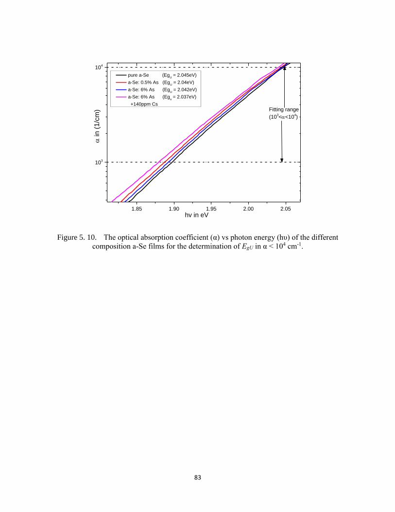
83
1.85 1.90 1.95 2.00 2.05
103
104
in
(1/c
m)
hv in eV
pure a-Se (EgU = 2.045eV)
a-Se: 0.5% As (EgU = 2.04eV)
a-Se: 6% As (EgU = 2.042eV)
a-Se: 6% As (Egu = 2.037eV)
+140ppm CsFitting range
(103<<10
4)
Figure 5. 10. The optical absorption coefficient (α) vs photon energy (hυ) of the different
composition a-Se films for the determination of EgU in α < 104 cm-1.

84
5.4 X-ray induced effects
In this experiment, the transmission spectrum of films was scanned before and after irradiating
X-rays for 20 minutes at the same spots. The reason for scanning the same spot of film twice is
to observe a change in thickness associated to X-ray irradiation. Also, to avoid aging effects, the
transmission spectrum was scanned right away once completing 20 minutes of exposure. The
samples were kept in the dark at room temperature between measurements, to avoid other
external stimuli.
We exposed different compositions of a-Se films (pure a-Se, a-Se:0.5% As, a-Se:6% As, and a-
Se:6% As: ppm Cs) the same dose of X-rays to observe composition influence and we also
irradiated each of the films under different dose of X-rays, a low dose at 30 kVp and a high dose
at 70 kVp to observe dose influence. The total delivered doses were approximately 943 Gy and
3148 Gy at 30 and 70 kVp radiation respectively with the total incident doses being 15.9 Gy and
44.0 Gy in air respectively. The calculation of dose in Se and air followed the method described
in Section 4.4, 4.5 and 4.6. The variation of density in As alloying or Cs doping was not taken in
account to calculate dose. The deposited energy in either pure a-Se or 0.5% As-alloyed a-Se was
assumed to be equivalent as long as the film thickness was the same, since alloy concentration is
very small.
The key point is photo contraction which accompanies an increase in the refractive index. The
photo-induced refractive index induced by a HeNe laser was also observed for a As2Se3 film [79]
and for As2Se3 and As2S3 films by UV exposure [80]. Also, the photo-induced effects of a-Se
turns out to be similar from aging effect in respect to optical changes. The aging effect gives a
decrease in d with an increase in n resulting from the structural relaxation [81].
Tanaka [82] proposed that there is a metastable state in a-Se during irradiation with the
excitation of lone-pair electrons from the VB to the CB. In this excited state, the dynamical
interchain bonds form between chains, increasing an atomic coordination number. Since this
bond is unstable, the bond breaking occurs, generating charged coordination defects (VAP)
which have been proven by ESR measurements from Kolobov [83] and time-of-flight
measurements from Walornyj [7]. It might be that there are some structural rearrangements

85
associated with defects generation, which is responsible for the thickness decrease.
Table 5.6 Optical properties of the four components of a-Se films (pure a-Se, a-Se:0.5%
As, a-Se: 6% As, a-Se: 6% As 140ppm Cs) before and after X-ray irradiation at 30 and 70 kVp.
Sample Treatment Dose
(Gy) Δd (nm)
d (nm)
n (λ=2000nm) ±0.0012
EgT
(eV) ±0.0007eV
EgU
(eV) ±0.0008eV
ΔE (meV) ±0.6meV
Pure a-Se Unirradiated 0 1816.7 ± 0.8 2.4666 2.0391 2.0457 65.81
30 kVp 949 0 1815.2 ± 0.8 2.4684 2.0388 2.0461 65.73
% change -0.082% 0.071% -0.014% 0.019% -0.114%
Unirradiated 11 1755.7 ± 0.8 2.4924 2.0416 2.0444 68.11
70 kVp 3160 11 1754.0 ± 0.8 2.4953 2.0407 2.0451 68.20
% change -0.101% 0.115% -0.043% 0.034% 0.135%
a-Se: 0.5% As
Unirradiated 0 1796.6 ± 0.8 2.4581 2.0370 2.0465 66.95
30 kVp 950 0 1794.5 ± 0.8 2.4613 2.0370 2.0467 66.89
% change -0.120% 0.129% 0% 0.013% -0.097%
Unirradiated 12 1495.5 ± 0.7 2.4753 2.051 2.0454 65.76
70 kVp 3164 13 1492.0 ± 0.7 2.4800 2.051 2.0458 66.25
% change -0.234% 0.188% 0.045% 0.016% 0.74%
a-Se:6% As
Unirradiated 20 3397.6 ± 1.5 2.4624 2.0007 2.0397 66.48
30 kVp 934 20 3392.7 ± 1.5 2.4659 2.0014 2.0400 66.29
% change -0.142% 0.141% 0.036% 0.015% -0.297%
Unirradiated 5 3552.1 ± 1.6 2.4705 1.9966 2.0426 65.59
70 kVp 3133 7 3545.8 ± 1.6 2.4749 1.9967 2.0426 65.60
% change -0.178% 0.178% -0.027% 0.001% 0.014%
a-Se:6% As +140 ppm Cs
Unirradiated 7 2993.6 ± 1.4 2.4541 1.9987 2.0387 67.20
30 kVp 938 8 2989.8 ± 1.4 2.4571 1.9984 2.0388 67.09
% change -0.127% 0.123% -0.016% 0.005% -0.164%
Unirradiated 14 3351.8 ± 1.5 2.4709 2.0042 2.0445 65.85
70 kVp 3136 15 3342.9 ± 1.5 2.4775 2.0034 2.0443 65.95
% change -0.267% 0.268% -0.043% -0.007% 0.15%
In Table 5.6, it was found that the refractive index n has increased and thickness d has decreased
upon X-ray irradiation. At 30 kVp irradiation, increases in n go from 0.07% (0.002) for pure a-
Se up to 0.12% (0.003) for a-Se 6% As + 140ppm Cs with decreases in d go from -0.08% (1.5
nm) up to -0.13% (3.8 nm). At 70 kVp irradiation, increases in n go from 0.12% (0.003) for
pure a-Se up to 0.27% (0.007) for a-Se 6% As + 140ppm Cs, with decrease in d from -0.10%
(1.7 nm) up to -0.27% (8.9 nm). It seems that 70 kVp has stronger X-ray effects than 30 kVp,
and there are composition effects upon X-ray irradiation. Figure 5.11 shows that the refractive
index was shifted up upon 70 kVp irradiation, and it was shifted further up with Cesium doping
in a-Se.

86
1000 1200 1400 1600 1800 2000
2.50
2.55
2.60
Ref
ract
ive
inde
x, n
Wavelength, nm
Unirradiated n = 2.471
a-Se: 6% As 70kVp n = 2.475
a-Se: 6% As 70kVp n = 2.478
+ 140ppm Cs
Figure 5. 11. Refractive index vs. wavelength for a-Se:6% As film (red curve) and a-Se:6% As
+140ppm Cs doped films (blue curve) before (black curve) and after irradiation at 70 kVp.
0.999
1.000
1.001
1.002
1.003
unirradiated
30 kVp (900 Gy)
70 kVp (3200 Gy)
n/n
o
(a)
0.997
0.998
0.999
1.000(b)
a-S
e
with 6
% A
s
140ppm
Cs
a-S
e w
ith
6%
As
a-S
e w
ith
0.5
% A
s
undoped
a-S
e
d/d
o
Figure 5. 12. The relative change of refractive index Δn/no, triangle symbols, and thickness
Δd/do, square symbols as a function of compositions in a-Se: pure a-Se, a-Se 0.5% As, a-Se 6%
As, a-Se 6% As + 140ppm Cs after irradiating at 30 kVp (red line) and 70 kVp (blue line). The
shaded area corresponds to statistical errors in Δd/d and Δn/n determination and is based on
assigning 2σ to the full width of error region.

87
The relative changes (Δn/no and Δd/do) for the different composition of a-Se were plotted in a bar
in Figure 5.12. It shows that X-ray effects for As alloying are weak, since the X-ray effects at 70
kVp go up with 0.5% As and down with 6% As, and the influence of Cs seems to be weak as
well. The relative percent changes in Δn/no and Δd/do in Figure 5.12 were plotted as a function of
the deposited dose in Figure 5.13. The 30 kVp in red bar and 70 kVp in blue bar correspond to
900 Gy and 3150 Gy in Figure 5.13. The X-ray effects increase gradually with increasing dose,
which implies that X-ray effects depend on the dose.
0 450 900 1350 1800 2250 2700 3150-0.3
-0.2
-0.1
0.0
0.1
0.2
0.3
d/d
(%
) &
n/n
(%
)
Dose (Gray)
a-Se
a-Se 0.5% As
a-Se 6% As
a-Se 6% As + 140ppm Cs
Figure 5. 13. The relative change of thickness (Δd/d), square symbols, and refractive index
(Δn/n), triangle symbols, in a-Se samples with varying compositions (dotted curves) as a function
of delivered (absorbed) dose in a-Se. a-Se, black; a-Se 0.5%, red; a-Se 6% As, green; a-Se 6%
As +140 ppm Cs, purple; after irradiation with 30 kVp (900 Gy) and 70 kVp (3150 Gy). Shaded
area corresponds to statistical errors in Δd/d and Δn/n determination and is based on assigning 2σ
to the full width of error region.
The increase in refractive index upon irradiating with X-ray is due to a density increase, that is
thickness decrease, possibly caused by structural re-arrangements. Using the Lorenz-Lorenz
relation from equation (2.20) above, change of Δn/no = 0.27% predicts a change (Δd/do)calc =
0.24%, which is close to the experimental change Δd/do =0.27% for a-Se 6% +140ppm Cs.
This correlation does not dependent on doped or pure samples or deposited doses. Otherwise,
Figure 5.12 and 5.13 would not show a symmetry between Δn/no and Δd/do.

88
Table 5. 7. Optical band gaps and its fitting parameters of the X-ray irradiation.
Tauc relation
αhυ = A (hυ− EgT) Urbach relation α = C exp (hυ/ ∆E)
Sample Treatment
A (cm-1)
EgT
(eV) ±0.0007 eV
EgU
(eV) ±0.0008 eV
C ×10-10
(cm-1) ΔE (meV) ±0.6 meV
RMSE
Pure a-Se Unirradiated 600839 2.0391 2.0457 3.1576 65.81 0.47
30 kVp 596204 2.0388 2.0461 3.0300 65.73 0.53
% change -0.77% -0.014% 0.019% -4.04% -0.114%
Unirradiated 616197 2.0396 2.0444 9.1845 68.11 0.52
70 kVp 609600 2.0393 2.0451 9.4660 68.20 0.50
% change -1.07% -0.019% 0.034% 3.07% 0.135%
a-Se 0.5% As Unirradiated 587180 2.0370 2.0465 5.3137 66.95 0.56
30 kVp 585704 2.0370 2.0467 5.1369 66.89 0.54
% change -0.25% 0% 0.013% -3.33% -0.097%
Unirradiated 669907 2.0505 2.0454 3.1075 65.76 0.42
70 kVp 676277 2.0515 2.0458 3.8863 66.25 0.42
% change 0.95% 0.046% 0.016% 25.0% 0.74%
a-Se 6% As Unirradiated 414232 2.0007 2.0397 4.74118 66.48 0.69
30 kVp 416577 2.0014 2.0400 4.30631 66.29 0.69
% change 0.57% 0.036% 0.015% -9.2% -0.297%
Unirradiated 382857 1.9966 2.0426 2.98776 65.59 0.81
70 kVp 383114 1.9967 2.0426 3.00025 65.60 0.82
% change 0.07% -0.0027% 0.001% 0.42% 0.014%
a-Se:6% As +140ppm Cs
Unirradiated 404384 1.9987 2.03867 6.67759 67.20 0.67
30 kVp 402327 1.9984 2.03878 6.34201 67.09 0.68
% change -0.51% -0.016% 0.005% -5.03% -0.164%
Unirradiated 415977 2.0042 2.04446 3.28331 65.85
70 kVp 412087 2.0034 2.04431 3.44727 65.95
% change -0.94% -0.043% -0.007% 5.00% 0.15%
From Table 5.7 above, the changes in EgT go from 0.043% to +0.046% within experimental
errors (±0.064%) and changes in EgU go from 0.007% to +0.034% within experimental errors
(±0.078%). The increase in n is supposed to accompany a decrease in EgT, known as the photo-
darkening effect, from Moss’s rule (Eg n4 ~ constant) [59]. The decrease in band gap also was
observed from Tanaka, by illuminating under band-gap light [84]. However, the change could
not be detected in this case and there was no clear pattern of decrease, as oppose to a gradual
change in n with respect to X-rays. There were lots of fluctuations in the extracted absorption
coefficient before and after irradiation.
The failure to observe photodarkening may be that the effects are too small to see the changes,
when considering that the maximum percent in d (or n) is below 0.3%. Also, it might be that the

89
beam spot in our spectrophotometry (i.e. around 18 mm2) is not too intense to produce detectable
photodarkening effects, as Tonchev reported [79]. Hence, further experiment is required to see
the photodarkening effects, such as using higher intensity of X-rays (i.e. 110 kVp) and a longer
exposure of X-rays to increase the delivered dose.
Table 5. 8. Wemple Di-Dominicio model parameters of X-ray irradiation.
𝑛𝑤𝑑2 = 1 +
𝐸0𝐸𝑑
𝐸02 − (ℎ𝑣)2
Treatment
nwd (at 2000nm)
Eo
(eV) ±0.005 eV
Ed (eV) ±0.035 eV
RMSE of fit
Pure a-Se Before #1 3rd 2.4573 3.75802 18.3902 1.89
After 30 kVp 4th 2.4589 3.75938 18.4249 1.91
% change 0.065% 0.036% 0.189%
Before #3 11th 2.4810 3.775 18.936 1.78
After 70 kVp 12th 2.4846 3.786 19.060 1.77
% change 0.148% 0.284% 0.651%
a-Se 0.5% As Before #2 17th 2.4482 3.771 18.324 1.92
After 30 kVp 18th 2.4510 3.773 18.381 1.92
% change 0.115% 0.034% 0.313%
Before #3 1st 2.4675 3.796 18.802 1.71
After 70 kVp 2nd 2.4719 3.797 18.885 1.71
% change 0.175% 0.022% 0.441%
a-Se 6% As Before #3 1st 2.4537 3.768 18.404 2.24
After 30 kVp 2nd 2.4567 3.770 18.469 2.22
% change 0.125% 0.047% 0.350%
Before 15th 2.4600 3.759 18.469 2.61 After 70 kVp 16th 2.4643 3.760 18.553 2.63
% change 0.177% 0.027% 0.453%
a-Se 6% As + 140ppm Cs
Before 17th 2.4454 3.768 18.255 2.37
After 18th30kVp 2.4484 3.768 18.310 2.38
% change 0.123% 0.002% 0.298%
Before #2 3rd 2.4609 3.771 18.550 2.52
After 70kVp 4th 2.4675 3.773 18.678 2.46
% change 0.267% 0.041% 0.681%
Table 5.8 above shows dispersion energy Ed and oscillator energy Eo obtained from fitting n to
the Wemple DiDominicio model. nwd, Eo and Ed are all increased after irradiation, but Eo
increases, which is within experimental errors (0.180%), and Ed increases by 0.441 0.681%,
which is beyond experimental errors (0.384%) for 70 kVp radiation. At 30kVp, Ed increases by
0.190.35% within errors. The increase in Ed is also affected by X-ray doses, as same as the n.

90
From equation Ed = β Nc ZaNe, where Nc is the effective coordination number of the cation
nearest-neighbor to the anion, increase in Ed is attributed to the increase of positively charged
defect Nc of VAP (Se3+). Since the X-ray induced charged defects of a-Se, Se1
- and Se3+, were
already proven from the time of flights measurements (i.e. X-ray induced defects increased the
concentration of the deep traps) [7], we expected that the increase in Ed is caused by an increase
in charged defects of VAP, Se3+. In addition, from the values of Eo in Table 5.9 and the EgT in
Table 5.8, it was found that Eo = 1.9×EgT,.
5.5 X-ray relaxation effects
This section examines whether the irradiated a-Se films return to its original states prior to
irradiation. After completing 20 minutes of 70 kVp X-ray irradiation, we let the films sit at room
temperature inside the spectrophotometry for two to three days and scanned the transmission
spectrum from 2 hours up to 3 days after irradiation to monitor its relaxation process. The
relaxation times used were: 2 hours, 3 hours, 14 hours and 3 days after X-ray irradiation. The
incident air doses for 70 kVp was 44 Gy and the deposited dose in a-Se 6% As was 3132 Gy.
Table 5.9 summarizes all key optical parameters before and after X-ray irradiation (The first two
rows list parameters before and right after X-ray irradiation, and the rest of the rows list those for
X-ray relaxation with elapsed time after completing irradiation).
Table 5. 9. Optical properties of X-ray reversibility of a-Se:6% As
In Table 5.9, there is a decrease in d on 0.14% with a corresponding increase in n on 0.14%,
upon X-ray irradiation at 70 kVp, and these d and n are fully recovered (0.09% and -0.09%
respectively) at least 14 hours after within the margin of error (±0.09%). It implies that the X-ray
Sample a-Se:6% As
Time (min)
Δd nm
d nm
n λ = 2000 nm ±0.0012
EgT eV ±0.0007 eV
EgU eV ±0.0008eV
ΔE meV ±0.6 meV
α cm-1 2.05 eV
Virgin 0 13 3541.2±1.6 2.46227 1.9960 2.0430 66.36 10422
70 kVp 25 min 13 3536.3±2.5 2.46570 1.9960 2.0434 66.41 10376 % change -0.139% 0.139% 0.001% 0.019% 0.081% -0.44%
70 kVp 25 min 13 3536.3±2.5 2.46570 1.9960 2.0434 66.41 10376
2hrs after 150 min 13 3536.2±2.5 2.46574 1.9959 2.0430 66.45 10436
3hrs after 210 min 13 3537.0±2.5 2.46522 1.9952 2.0431 66.42 10427
14hrs after 850 min 13 3539.5±2.5 2.46345 1.9958 2.0433 66.43 10400
3days after 4080 min 13 3542.5±2.5 2.46139 1.9960 2.0430 66.42 10430
% change 0.175% -0.175% 0.001% -0.021% 0.013% 0.52%

91
induced optical properties are reversible and suggests that there are also structural
rearrangements occurring with elapsed time [54]. In Figure 5.14 where X-ray effects were
plotted as a function of logarithmic time, there is a consistent and gradual return of d and n to
original values. It also shows that changes in d and n are co-related according to the Claudius-
Mossotti relationship, which implies that there is no change in polarizability at all.
Moreover, two optical band gaps are changed with elapsed time after X-ray irradiation. The EgU
seems to increase 0.02% upon irradiation and reverse back as relaxing, but EgT is not reversed
back. However, both optical gaps are changed only within an experimental error unlike change in
refractive index and thickness. Therefore, there is no change in band-gap on relaxation, in which
same case as X-ray irradiation in Section 5.4.
0.1 1 10 100 1000 10000
-0.2
-0.1
0.0
0.1
0.2
d
/do a
nd
n
/no
Time (min)
d/do
n/no
70kVp 2hrs after
3hrs after
14hrs after3 days
after
Figure 5. 14 The 70kVp irradiation and time evolution of the thickness Δd/do and refractive
index Δn/no, during and after X-ray irradiation, where do and no are the initial thickness and
refractive index of a-Se:6% As virgin film. The 70kVp label refers to the end of irradiation (The
error bars represent maximum possible error in here).

92
Table 5. 10. Wemple Di-Dominicio coefficients of X-ray relaxation.
𝑛𝑤𝑑2 = 1 +
𝐸0𝐸𝑑
𝐸02 − (ℎ𝑣)2
Sample a-Se 6% As
Time nwd (at 2000nm)
Eo
(eV) ±0.005 eV
Ed (eV) ±0.035 eV
RMSE of fit (%)
Virgin 21:00 Jan 6 2.4526 3.7615 18.351 2.45
70 kVp Irradiated 21:25 Jan 6 2.4560 3.7623 18.417 2.47
% change 0.139% 0.021% 0.360%
70 kVp Irradiated 21:25 Jan 6 2.4560 3.7623 18.417 2.47
2hrs after 23:30 Jan 6 2.4560 3.7623 18.418 2.48
3hrs after 24:30 Jan 6 2.4555 3.7622 18.408 2.47
14hrs after 11:19 Jan 7 2.4537 3.7618 18.374 2.46
3 days after 17:14 Jan 9 2.4517 3.7613 18.335 2.47
% change -0.175% -0.027% -0.445%
In Table 5.10, the Sellmeier dispersion relationship of refractive index was fitted in the Wemple
Di-Dominicio dispersion to analyze the optical constants of Ed and Eo after completing X-ray
irradiation. The increase in dispersion energy Ed on X-ray irradiation is balanced by its decrease
on X-ray relaxation. The increase in Ed by 0.36% during irradiation decreases by 0.23% with
relaxation. The increase in Ed arises from the increase in Nc of defects Se3+ upon 70 kVp
irradiation from Section 5.4, and the decrease in Ed is related to the decrease in Nc of defects Se3+
during X-ray relaxation. So, it implies that X-ray induced defects are annealed over time as
relaxing. This is agreement with Walornyj [7], in which defects creation upon X-ray irradiation
is balanced by their removal from the X-ray recovery on studying electron lifetime during X-ray
irradiation and recovery. Kolobov [85] also described that X-ray relaxation is a process of
annihilation of defects. In addition, the oscillator energy Eo is changed within experimental
errors. In conclusion, the X-ray induced change in d, n and Ed in a-Se is reversible.

93
Chapter 6. Summary and Conclusion
In Section 5.1 upon heating an a-Se film (up to 6%As and with 140 ppm Cs) at Tg, we observed a
decrease in n due to the decrease in density (increase in d) arising from the structural expansion
at the phase transition near Tg. The n and d changes could be explained by using the Clausis-
Mossotti equation.
∆𝑛
𝑛𝑜 =
−(𝑛𝑜2 − 1)(𝑛𝑜
2 + 2)
(6𝑛𝑜2)
∆𝑑
𝑑0 (6.1)
The observed (Δd/do) of 1.51 % calculates a drop of (Δn/no)calc of 1.72 %, which is close to the
observed value (Δn/no) of 1.2 %, which implies that the 70% of (Δn/no) change can be
attributed to the change in the density. The decrease in optical gap EgT correlates well with the
decrease in the density.
It was also observed that heating results in a decrease in dispersion energy Ed, which can be
attributed to the decrease in the effective coordination number Nc of positively charged defects of
Se3+ in VAP according to the relation: Ed = β Nc Za Ne. This change in Nc was due to an increase
in intermolecular distance at the phase transition near Tg. There was decrease in the oscillator
energy Eo. It was found that Eo ≈ 1.89× EgT.
It was shown in Section 5.3 that alloying with As and doping with Cs of a-Se films gave arise to
an increase in n. The increase in n by alloying with up to 6% As was due to an increase in the
concentration of atoms, not polarizability, using the Clausius-Mossotti. In the case of Cs doping,
however, the increase in n is probably due to ionic polarizability or due to additional VAP
dipoles that would be created by Cs in the structure. It was found out that the increase in n from
alloying and doping of a-Se also leads to the decrease in the Tauc band-gap, as expected from
Moss’s rule: Eg n4 = constant.

94
In Section 5.4 and 5.5, X-ray irradiation increase leads to an increase in n with an increase in the
density (decrease in thickness d) due to structural rearrangements. The changes were reversed
back to the equilibrium values with relaxation over 16 hours, as a-Se films are structurally
relaxing. The X-ray induced changes were affected by the deposited dose, that the x-ray induced
refractive index on 70 kVp (3150 gray) was much stronger than 30 kVp (940 gray) radiation.
The X-rays did not induce any changes in two the optical gaps EgT and EgU at all, in contrast to
the gradual and clear changes in n and d beyond experimental errors. Although the changes in n
and d were discernable, it turns out these changes were very small (maximum 0.27%) compared
to the change induced by heating (maximum 2.2%).
The refractive index n was fitted into the Wemple-DiDominicio relationship to show the increase
in the dispersion energy Ed is related to the increase in the effective number of coordination
number Nc (defect creation) and to show the decrease in Ed is related to the decrease in Nc upon
X-ray relaxation (defect annihilation). The defect creation and annihilation due to X-rays were in
agreement with the experiments done by interrupted field time of flights measurements. The
relationship between Eo and EgT was found out to be Eo = 1.9×EgT.
Table 6. 1. Summary of optical properties for a-Se films.
Description
Sec
d (nm)
n (at λ = 2000nm)
EgT
(eV) EgU (eV)
Heating to Tg 5.1 increase decrease decrease decrease
Increased thickness
5.2 n/a -- -- --
Alloying As 5.3 n/a increase decrease decrease
Doping Cs 5.3 n/a increase decrease decrease
X-ray irradiation 5.4 decrease increase no change --
X-ray relaxation 5.5 increase decrease no change --

95
References
[1] G. J. Bansal, “Review: Digital radiography: A comparison with modern conventional
imaging”, Postgraduate Medical Journal, Vol 82, Issue 969, pp 425–428, 2006.
[2] M. Körner, C. H. Weber, S. Wirth, K. J. Pfeifer, M. F. Reiser, and M. Treitl, Advances in
Digital Radiography: Physical Principles and System Overview, RadioGraphics Education
Exhibit., Vol 27, Issue 3, pp 675 – 686, 2007.
[3] S.O. Kasap and J.A. Rowlands, “Direct-conversion flat-panel X-ray image detectors”, IEE
Proceedings - Circuits, Devices and Systems, Vol 149, No 2, pp 85-96, April 2002.
[4] S.O. Kasap, M. Z. Kabir, J.A. Rowlands, “Recent advances in X-ray photoconductors for
direct conversion X-ray image detectors”, In Current Applied Physics, Volume 6, Issue 3, pp
288-292, 2006.
[5] M. Spahn, “Flat detectors and their clinical applications”, European Radiology, Vol 15, Issue
9, pp 1934–1947, 2005.
[6] L. Bakueva, A. W. Rau, J. A. Rowlands and A. Shik, “X-ray-induced ghosting in amorphous
selenium”, Journal of Physics D: Applied Physics, Vol 39, No 3, pp. 441- 448, January 2006.
[7] M. Walornyj and S. O. Kasap, “X-ray irradiation induced changes in electron transport in
stabilized a-Se photoconductors”, Journal of Applied Physics, Vol 114, Issue 21, pp. 214505,
2013.
[8] S.O. Kasap and J.A. Rowlands, “Review: X-ray photoconductors and stabilized a-Se for
direct conversion digital flat-panel x-ray image-detectors”. Journal of Materials Science:
Materials in Electronics, Vol 11, Issue 3, pp 179–198, April 2000.

96
[9] P. Sprawls, “X-Ray Image Formation and Contrast”, The Physical Principles of Medical
Imaging, Medical Physics Publishing, 1995, Second edition,
http://www.sprawls.org/ppmi2/XRAYCON/ (Accessed at Dec 2016).
[10] P. Sprawls, “X-ray Production”, The Physical Principles of Medical Imaging, Medical
Physics Publishing, 1995, Second edition, http://www.sprawls.org/ppmi2/XRAYPRO/
(Accessed at Dec 2016).
[11] A.C. Carl and A.C. Gudrun. Basic physics of X-ray imaging. Department of Medicine and
Care Radio Physics, Faculty of Health Science, 2017.
[12] J.A. Seibert, “Digital radiography: The bottom line comparison of CR and DR technology”,
Applied Radiology, pp. 21- 28, 2009.
[13] B. J. Fogal, Electronic Transport Properties of Stabilized Amorphous Selenium X-ray
Photoconductors, MSc thesis, University of Saskatchewan, 2005.
[14] L. Lanca and A. Silva, “Chapter 2: Digital Radiography Detectors: A Technical Overview”
in Digital Imaging Systems for Plain Radiography, 2013, Springer New York.
[15] G. S. Ristić, “The digital flat-panel X-ray detectors”, Proceedings of the third conference on
medical physics and biomedical engineering, Association for medical physics and biomedical
engineering in cooperation with the European federation of organisations for medical physics,
page 65- 71, 2013 October.
[16] V. F. Andolina, S. Lile, Mammographic imaging: A practical guide, third edition,
Philadelphia, Penn.: Wolters Kluwer/Lippincott Williams & Wilkins Health, c2011.
[17] S.O. Kasap, “X-ray sensitivity of photoconductors: application to stabilized a-Se”, Journal
of physics D: Applied physics, Vol 33, No 21, pp 2853–2865, 2000.
[18] V. I. Mikla and V. V. Mikla, Amorphous Chalcogenides: The Past, Present, and Future,
Elsevier Inc. 2011.
[19] G. K. Ahluwalia, Applications of Chalcogenides: S, Se, and Te, Springer International
Publishing, November 2016.

97
[20] J. Rowlands and S. O. Kasap, “Amorphous semiconductors usher in digital x-ray imaging”,
Physics Today, pp 24- 30, 1997.
[21] M. A. Popescu, Non-Crystalline Chalcogenides, Solid state science and technology library,
Kluwer Academic Publishers, 2006.
[22] Y. Sakaguchi and K. J. Tamura “Photodarkening process in amorphous chalcogenide;
Measurements of transient photo-induced optical absorption”, Journal of Materials Science:
Materials in Electronics, Vol 18, Supplement 1, pp 459–462, October 2007.
[23] F. Djefaflia, C. Mebarkia, A. Hafdallah, M.L. Benkhedir, A. Belfedal, “Photoinduced
changes in amorphous selenium”, Canadian Journal of Physics, Vol 92, pp 663-666, 2014.
[24] J. Teteris, “Holographic recording in amorphous chalcogenide thin films, Current Opinion
in Solid State and Materials Science”, Vol 7, Issue 2, pp 127–134, April 2003.
[25] C. Juhasz and V. Gembala, “Growth characteristics of vacuum coated thick a-Se films for
device applications”, Journal of Vacuum Science & Technology A: Vacuum, Surfaces, and
Films, Vol 18, 665, 2000.
[32] S. O. Kasap, Principles of Electronic Materials and Devices, McGraw-Hill Inc, Third
Edition, 2006.
[33] W. H. Zachariasen, “The Atomic Arrangement in Glass”, Journal of the American Chemical
Society, Vol 54, (10), pp 3841–3851, 1932.
[34] J. A. Woollam, K. R. Morasb, M. Kzlninsky, and B. L. Averbach, “Photoconductive and
Optical Properties of Amorphous Selenium”, Lewis research center, National Aeronautics and
Space Administration (NASA), Washington, D.C., 1971.
[35] T. Merdzhanova, “Chapter 2”, Microcrystalline Silicon Films and Solar Cells Investigated
by Photoluminescence, Forschungszentrums Jülich in der Helmholtz-Gemeinschaft, Vol 41,
2005.
[36] M. L. Benkhedir, Defect Levels in the Amorphous Selenium Bandgap, PhD thesis,
Katholieke Universiteit Leuven, 2006.

98
[37] K. Koughia, Z. Shakoor, S. O. Kasap, and J. M. Marshall, “Density of localized electronic
states in a-Se from electron time-of-flight photocurrent measurements”, Journal of Applied
Physics, 97, 033706, 2005.
[38] C.K. Wong, G. Lucovsky, J. Bernholc, “Intrinsic localized defect states in a-Se associated
with dihedral angle distortions”, Journal of Non-Crystalline Solids, Vol 97–98, Part 2, pp. 1171-
1174, 1987.
[39] G. Lucovsky and F. L. Galeener, “Intermediate ranger order in amorphous solids”, Journal
of Non-Crystalline Solids, Vol 35-36, part 2, pp. 1209- 1214, 1980.
[40] M. Kastner, D. Adler, H. Fritzsche, “Valence-Alternation Model for Localized Gap States in
Lone-Pair Semiconductors”, Physical Review Letters, Vol 37, No 22, pp. 1504- 1507, 1976.
[41] B.W. Corb, W.D. Wei and B.L. Averbach, “Atomic models of amorphous selenium”,
Journal of Non-Crystalline Solids, Vol 53, Issue 1-2, pp. 29-42, 1982.
[42] C. Koughia, A. Reznik, C. Allen, R. Johanson, and S. Kasap, “Density of localized state
distribution near the valence band in stabilized a-Se using interrupted field time of flight
measurements with long interruption times”, Physica Status Solidi A, Vol 213, Issue 7, pp. 1856-
1863, 2016.
[43] W. C. Tan, Optical Properties of Amorphous Selenium Films, MSc thesis, University of
Saskatchewan, July 2006.
[44] M. Abkowitz and R. C. Enck, “Xerographic spectroscopy of gap states in amorphous
semiconductors”, Physical Review B, Vol 25, No 4, pp. 2567 – 2577, 1982.
[45] J. Berashevich, A. Mishchenko, and A. Reznik, “The two-step photoexcitation mechanism
in amorphous Se”, Physical Review Applied, Vol 1, Issue 3, pp. 34008, 2014.
[46] R. Swanepoel, “Determination of the thickness and optical constants of amorphous silicon”,
Journal of Physics E: Scientific Instruments, Vol 16, 1983, pp. 1214 – 1222.

99
[47] R. swanepoel, “Determination of surface roughness and optical constants of inhomogeneous
amorphous silicon films”, Journal of Physics E: Scientific Instruments, Vol 17, 1984, pp. 896 –
903.
[48] S. Ahmad and M. Mohib-ul Haq, “A study of energy gap, refractive index and electronic
polarizability of ternary chalcopyrite semiconductors”, Iranian Journal of Physics Research, Vol
14, No 3, pp. 89-93, 2014.
[49] M. H. Saleh, M. M. Abdul-Gader Jafar, B. N. Bulos, and T. M. F. Al-Daraghmeh,
“Determination of Optical Properties of Undoped Amorphous Selenium (a-Se) Films by
Dielectric Modeling of Their Normal-Incidence Transmittance Spectra”, Applied Physics
Research, Vol 6, No 6, 2014, pp. 10- 44.
[50] S. Kugler and K. Shimakawa, Amorphous Semiconductors, Cambridge University Press,
United Kingdom, 2015.
[51] S. Kasap, C. Koughia, J. Singh, H. Ruda, and S. O’ Leary, “Chapter 3: Optical properties of
electronic materials: Fundamentals and characterization”, Springer handbook of electronic and
photonic materials, edited by S. Kasap and P. Capper, springer US, 2007.
[52] M. Nessa, K. Shimakawa, A. Ganjoo, and J. Singh. “Fundamental optical absorption on
fractals: A case example for amorphous chalcogenides”, Journal of Optoelectronics and
Advanced Materials, Vol 2, No 2, pp. 133-138, June 2000.
[53] N.F. Mott and E.A. Davis, Electronic processes in non-crystalline materials, second edition,
Oxford: clarendon press, p 272, 1905.
[54] K. Tanaka and K. Shimakawa, Amorphous chalcogenide semiconductors and related
materials, Springer New York Dordrecht Heidelberg London, 2011.
[55] L. Tichy, H. Ticha, P. Nagels, E. Sleeckx and R. Callaerts, “Optical gap and Urbach edge
slope in a-Se”, Materials Letters, Vol 26, Issue 6, pp. 279-283, 1996.
[56] K. Tanaka, T. Gotoh, N. Yoshida, S. Nonomura, “Photothermal deflection spectroscopy of
chalcogenide glasses”, Journal of Applied Physics, Vol 91, pp. 125, 2002.

100
[57] J.M.González -Leal, Mir.Vlček, R.Prieto-Alcón, A.Stronski, T.Wágner, E.Márquez,
“Thermal relaxation of the structural and optical properties of amorphous AsSSe films”, Journal
of Non-crystalline solids, Vol 326 & 327, 2003, pp. 146 – 153.
[58] Y.H. Jung, O. Güneş, G. Belev, C. Koughia, R. Johanson, S. Kasap, “X-ray induced effects
in the optical and thermal properties of a-Se1−xAsx (x = 0, 0.005, 0.06) doped with 0–220 ppm
Cs”, Journal of Materials Science: Materials in Electronics, Vol 28, Issue 10, pp 7139–7150,
2017.
[59] T. S. Moss, “Relation between the refractive index and energy gap of semiconductors”
Physica Status Solidi B, 131, pp. 415-427, 1985.
[60] P. Hervé and L. K. J. Vandamme, “General relation between refractive index and energy
gap in semiconductors”, Infrared Physics and Technology, Vol 35, Issue 4, pp. 609-615, 1994.
[61] OJL interband transition model for amorphous materials - a brief tutorial, Optical transitions
in amorphous materials. http://www.mtheiss.com/ojl_optr.htm (Accessed at Dec 2016).
[62] D. Dorrania n, L. Dejam and G. Mosayebian, “Optical characterization of Cu3N thin film
with Swanepoel method”, Journal of Theoretical and Applied Physics, Vol 6, Issue 13, pp. 1-9,
2012.
[63] S. O. Kasap, “Chapter 1: Wave nature of light”, Optoelectronics and Photonics: principles
and practices, Second edition, Pearson Education, 2013.
[64] D. Poelman and P. F. Smet, “Methods for the determination of the optical constants of thin
films from single transmission measurements: a critical review”, Journal of Physics D: Applied
Physics, Vol 36, No 15, pp, 1850-1857, 2003.
[65] P. Nagels, E. Sleeckx, R. Callaerts, E. Márquez, J.M. González, A.M. Bernal-Oliva,
“Optical properties of amorphous Se films prepared by PECVD”, In Solid State
Communications, Vol 102, Issue 7, pp. 539-543, 1997.
[66] J. Yang, X-ray Induced Changes in Electronic Properties of Stabilized Amorphous Selenium
Based Photoconductors, MSc, University of Saskatchewan, 2016.

101
[67] P. Sprawls Jr, “Interaction of radiation with matter”, The Physical Principles of Medical
Imaging, Medical Physics Publishing, 1995, Second edition,
http://www.sprawls.org/ppmi2/INTERACT/ (Accessed at Dec 2016).
[68] https://www.oem-xray-components.siemens.com/x-ray-spectra-simulation (Accessed Jan
2017).
[69] P. Sprawls Jr, “Radiation quantities and units”, The Physical Principles of Medical Imaging,
Medical Physics Publishing, 1995, Second edition. http://www.sprawls.org/ppmi2/RADQU/
(Accessed at Dec 2016).
[70] http://physics.nist.gov/PhysRefData/XrayMassCoef/ElemTab/z34.html (Accessed Jan 2017)
[71] Instrumental specification for Lambda 900.
[72] G. Okada, Development of a Large-Dose, High-Resolution Dosimetry Technique for
Microbeam Radiation Therapy using Samarium-Doped Glasses and Glass-Ceramics, PhD
thesis, University of Saskatchewan, 2014.
[73] M. I. Ojovan, “Configurons: Thermodynamic Parameters and Symmetry Changes at Glass
Transition”, Entropy, Vol 10, Issue 3, pp 334-364, 2008.
[74] S.O. Kasap, “Photoreceptors: The Chalcogenides”, Chapter 9 in The Handbook of Imaging
Material: Second Edition Revised and Expanded, edited by Arthur S. Diamond and David S.
Weiss, Marcel Dekker Inc., New York, pp. 343-346, 2002.
[75] R.K. Kirby and B.D. Rothrock, “Thermal expansion of vitreous selenium from -190 to 30°
C”, Journal of the American Ceramic Society- Discussion and notes, pp 535, 1968.
[76] E.R. Shaaban, “Calculation of the optical constants of amorphous semiconducting As40S60,
As40S35Se25 and As40Se60 thin films from transmittance and reflectance measurements”.
Journal of Applied sciences, Vol 6, Issue 2, pp 340 – 346, 2006.
[77] J. Pétursson, J. M. Marshall and A. E. Owen, “Optical absorption in As-Se glasses”,
Philosophical Magazine B, Vol 63, Issue 1, pp 15-31, 1991.

102
[78] Z.U. Borisova, Glasses in Binary Systems. In: Glassy Semiconductors, pp 38-39,
Springer, Boston, MA, 1981.
[79] A. C. van Popta, R. G. DeCorby, C. J. Haugen, T. Robinson, J. N. McMullin, D. Tonchev,
and S. O. Kasap, “Photoinduced refractive index change in As2Se3 by 633nm illumination”,
Optics Express., Vol 10, Issue 15, pp 639-644, 2002.
[80] P. Bhardwaj, P. K. Shishodia, R. M. Mehra, “Photo-induced changes in optical properties
of As2S3 and As2Se3 films deposited at normal and oblique incidence”, Journal of Materials
Science, Vol 38, Issue 5, pp 937–940, March 2003.
[81] W. C. Tan, G. Belev, K. Koughia, R. Johanson, S. K. O’Leary, S. Kasap, “Optical
properties vacuum deposited and chlorine doped a-Se thin films: aging effects”, Journal of
materials science: Materials electronics, Vol 18, pp. S429–S433, 2007.
[82] A.V. Kolobov, H. Oyanagi, K. Tanaka, Ke Tanaka. “An in situ EXAFS study of amorphous
selenium: The formation of dynamical bonds under light excitation”, Journal of Luminescence,
Vol 66 and 67, pp 174-178, 1995.
[83] A.V. Kolobov, M. Kondo, H. Oyanagi, R. Durny, A. Matsuda, K. Tanaka, “Experimental
evidence for negative correlation energy and valence alternation in amorphous selenium”,
Physical review B, Vol 56, No 2, pp. R485 -R488, 1997.
[84] K. Tanaka and A. Odajima, “Photo darkening in amorphous selenium”, Solid State
Communications, Vol 43, No 12, pp. 961-964, 1982.
[85] A. V. Kolobov, photo-induced metastability in amorphous semiconductors, John Wiley &
Sons, 2006.
[86] M. L. Trunov, P. M. Lytvyn, S. N. Yannopoulos, I. A. Szabo, and S. Kokenyesi,
“Photoinduced mass-transport based holographic recording of surface relief gratings in
amorphous selenium films”, Applied Physics Letters, Vol 99, pp.51906, 2011.