Write your four digit code here .. NEW MEXICO
32
Write your four digit code here .........................................
Transcript of Write your four digit code here .. NEW MEXICO

Write your four digit code here .........................................
NEW MEXICO STATE UNIVERSITY THE KLIPSCH SCHOOL OF ELECTRICAL AND COMPUTER
ENGINEERING Ph.D. QUALIFYING EXAMINATION
August 16, 2010 9:00 AM - 1:00 PM CLOSED BOOK
Exam Instructions:
a. Write the last four digits of your Banner ID number on the top of every page.
b. Work six (6) problems from the three (3) areas of specialization
selected at the time of registration. Do not work more than two (2) problems in any one area.
A Circuits and Electronics B Communications C Computers D Control Systems E Digital Signal Processing F Electric Energy Systems G Electromagnetics H Photonics
c. Check the boxes below indicating which six (6) problems you
want graded. (You must work two problems from each of the three areas you specified at the time of registration.)
a b c d e f
A Circuits and Electronics.
B Communications…………..
C Computers…………………
D Control Systems.…...........
E Digital Signal Processing
F Electric Energy Systems.
G Electromagnetics.............
H Photonics………………......

Design a fully-differential telescopic operational amplifier for a minimum gain-bandwidth product GB=100MHz and a load capacitance CL=10pF. Assume following 0.18um CMOS technology parameters: knn=170μA/V2, Vthn=0.45V, knp=25uA/V2, Vthp=0.45V, λn=λp=0.1V-1, Cox=4.2fF/μm2 and a capacitive load CL=10pF (kn=μCox). Determine all transistor sizes including those in the biasing branch. Assume a single supply voltage Vdd=1.8V The design requires to determine bias currents and W/L sizes for all transistors. Estimate for your design: a) location of the dominant pole and second (high frequency) pole taking into account only gate-source (Cgs) parasitic capacitances (do not take into account Cgd, Cbd and Csb parasitic capacitances) the open loop gain and the slew rate of the op-amp.
A (a) Circuits and Electronics

Design a single-ended two stage operational amplifier for a minimum gain-bandwidth product GB=10MHz and a load capacitance CL=50pF. Assume following 0.18um CMOS technology parameters: knn=170μA/V2, Vthn=0.45V, knp=25uA/V2, Vthp=0.45V, λn=λp=0.1V-1, Cox=4.2fF/μm2 (kn=μCox). Determine all transistor sizes including those in the biasing branch. Assume a single supply voltage Vdd=1.8V The design requires to determine bias currents, W/L size all transistors, and to determine the value of the compensation capacitance. Estimate for your design: a) location of the dominant pole and second (high frequency) pole taking into account only gate-source (Cgs) parasitic capacitances (do not take into account Cgd, Cbd and Csb parasitic capacitances) the open loop gain and the slew rate of the op-amp.
A (b) Circuits and Electronics

1) Explain what are the main design constraints faced by analog designers in modern deep submicrometer (fine line) CMOS technology
2) a) Explain the three types of random mismatch errors in analog circuits. b) What layout techniques are used to minimize the effect of each type of mismatch error? Justify your answers
A (c) Circuits and Electronics

Consider the two random variables X1 and X2 with joint pdf
fX1,X2(x1, x2) =
{116 for |x1| < 4, 2 < x2 < 4,0 otherwise.
Determine whether X1 and X2 are independent and/or orthogonal.
B (a) Communications

Consider the following moving average process Yn = 1/2·(Xn+Xn−1) whereXn is a wide sense stationary(WSS) random process (n = 0, 1, 2, . . . ).
(a) Determine whether Yn is a WSS random process.
(b) Sketch the autocorrelation sequence of Yn and determine the power spectral density SY Y (ejω).
B (b) Communications

Let the lifetime of a device be an exponential random variable with a mean of 24 hours. Suppose that 20devices are tested and their lifetimes are measured, where the measurements are assumed to be independentof each other. Determine an estimate of the probability that the sum of the lifetimes is less than 500 hoursby using the Central Limit Theorem.Hint: For an exponential random variable X with pdf
fX(x) ={λe−λx, x ≥ 0,
0, x < 0.
and parameter λ, we have E(X) = 1/λ and Var(X) = 1/λ2. A Q-function table is attached.
B (c) Communications

B (c) Communications

The throughputs of two networking systems are measured 7 times. The mean (m) and standard deviation (s) of the sample throughput differences are 1.05, 1.62, respectively. Can we say with 99% confidence that one system is better that the other (the confidence interval does not include zero)? t[0.995, 6] =3.707.
C (a) Computers

Suppose we use an M/M/1 queue to model a restaurant. Customers come to a restaurant at an average rate of 4 per hour. Each customer spends an average of half an hour eating the meal (excluding waiting time). What is the average number of customers in the restaurant? What is the probability that there are more than 10 customers in the restaurant?
C (b) Computers

Two random variables, x, y, are measured in an experiment, and their means and variances are E[x]=2, Var[x]=4, and E[y]=3, Var[y]=4, respectively. Suppose the linear regression model turns out to be: y = 0.5 x + 2. What is the covariance between the two random variables? What is the coefficient of determination (R2) of the regression model?
C (c) Computers

You are building a system around a processor with in-order execution that runs at 2.0 GHz and has a CPI of 0.7 excluding memory accesses. The only instructions that read or write data from memory are loads (20% of all instructions) and stores (5% of all instructions). The memory system for this computer is composed of a split L1 cache that imposes no penalty on hits. Both the I-cache and D-cache are direct-mapped and hold 32KB each. The I-cache has a 3% miss rate and 32-byte blocks; the D-cache is write through with a 5% miss rate and 16-byte blocks. There is a write buffer on the D-cache that eliminates stalls for 95% of all writes. The 512KB write-back, unified L2 cache has 64-byte blocks and an access time of 15ns. It is connected to the L1 cache by a 128-bit data bus that runs at 266MHz and can transfer one 128-bit word per bus cycle. Of all memory references sent to the L2 cache in this system, 82% are satisfied without going to main memory. Also, 50% of all blocks replaced are dirty. The 128-bit-wide main memory has an access latency of 60ns, after which any number of bus words may be transferred at the rate of one per cycle on the 128-bit-wide 166MHz main memory bus.
a. What is the average memory access time for instruction accesses?
b. What is the average memory access time for data writes? c. What is the overall CPI, including memory accesses?
C (d) Computers

Consider a dynamically scheduled, speculative, microprocessor with one load/store unit, one floating-point add unit, one integer add unit, and one floating-point multiplication unit. Assume that the arithmetic units are pipelined and that each functional unit has two reservation stations. Further assume that the instruction buffer (issue queue) holds at most eight instructions and that eight instructions can be fetched and issued simultaneously. If you feel that you must assume instruction execution latencies, state your assumptions. a. Give an instruction sequence that causes a stall due to a full instruction buffer. Briefly explain why your scenario causes this type of stall. b. Give an instruction sequence that causes a functional unit to stall, i.e., that causes a functional unit (at least one segment of its pipeline) to be idle. c. Assume that a branch is mispredicted. Explain when this is noticed and what happens
as a result of this situation.
C (e) Computers

Consider caches. a. Do ALL caches require that each cache line have a dirty bit? Why or why not?
b. Do ALL caches require that on a write miss the missed cache line be fetched from the next level of the memory hierarchy? Why or why not?
c. Does enlarging the cache ALWAYS give an application a better hit rate? Why or why not?
C (f) Computers

If (A,C) is detectable, and there exists P > 0 such that AT P + PA − PBBT P + CTC + 3P = 0
show that the matrix A + BK, K = −BT P
has eigenvalues with real parts less than –1.
D (a) Control Systems

For the discrete-time system
x t +1( )=32 1
− 12 0
⎡
⎣ ⎢
⎤
⎦ ⎥ x +
01
⎡
⎣ ⎢
⎤
⎦ ⎥ u, x 0( )=
4−4
⎡
⎣ ⎢
⎤
⎦ ⎥
find a control sequence, , , to drive the state from the initial state to the final state
u t( ) t = 0,1,2,...
x 2( )=4−2
⎡
⎣ ⎢
⎤
⎦ ⎥
and then maintain that state for all t . ≥ 2
D (b) Control Systems

Given the scalar system Ý x = 2x − u + w, y = 2x
with a disturbance given by
w t( )= M + N cos 2t +12°( )us t − 7( )
where M, N are unknown values with M ∈ .5,5[ ],N ∈ 2,3[ ]. It is desired that the system
track the sinusoid
r t( )= 1+ 2sin 2t( )
and settle within 1 second. Design an output-feedback controller to make this happen.
D (c) Control Systems

Consider a digital filter whose transfer function has a single pole at z = 1/2, a single poleat z = 0, and two zeros at z = −1. The transfer function includes a scale factor so that theDC response is 0 dB.
(a) Sketch the pole-zero pattern of the filter.
(b) Determine the transfer function H(z). Be sure to include (and determine) the scalefactor.
(c) Assume the filter is stable and determine the impulse response h[n].
(d) Sketch the magnitude response of the filter |H(ejω)| vs. ω for 0 ≤ ω ≤ π.
E (a) Digital Signal Processing

(a) Assume that a binary word represents the amplitude of a signal. For a signed integerbinary word length of b+ 1 bits (one sign bit and b magnitude bits), determine the dynamicrange in decibels (dB) defined by
dynamic rangedB = 20 log10
(largest possible word value
smallest possible word value
).
Your expression should only be a function of b.
(b) Show that your expression in (a) can be approximated as
dynamic rangedB ≈ 20 log10
(2b)≈ 6.02 · b (dB)
(c) Use the simplified result in (b) to explain why a 16 bit analog-to-digital (A/D) convertermight be preferred over 8 bit A/D converter for high-fidelity audio.
E (b) Digital Signal Processing

PROBLEM DSP: Linear Phase filters
a) (3 pts) Define the frequency response of a generic linear phase filter. Why is linearphase an important property to have in a filter? Can infinite impulse response filters everbe linear phase under any circumstances? Explain.
b) (3 pts) To achieve linear phase, a filter must have either a symmetric or anti-symmetric impulse response. Assume that the impulse response of the filter is given byh[n] where 0 ! n ! N. Write the symmetry and anti-symmetry equations in terms of h[n]for a generic linear phase system.
c) (2 pts) Derive the z-transform domain relation that must be satisfied for any linearphase system.
d) (2 pts) Given that h[n] is real and linear phase and that the corresponding z-transformH(z) has zeros at -0.75 and (1.25 � j2). What other zeros must H(z) have? Note: thisanswer can be calculated from the relation of c) if you have not memorized it.
E (c) Digital Signal Processing

1 2 Generator Transformer 1 MVA 2 MVA 60 Hz, 4160 V 4160 Delta – 480 Yg Wye grounded Xo=X1=X2=0.1pu Xd”=0.2, X2=0.18,Xo=.1pu
X
Sketch the sequence Thevenin networks as seen from bus 2 Tell me how these networks would be connected for the following faults
Three phase Single line to ground Line-line-ground through fault impedance
For a single line-ground fault at X Find the line currents and line to ground voltages at the terminals of the generator
F (a) Electric Energy Systems

Figure 1 shows a single-line diagram of a three-phase, 60-Hz synchronous generator, connected through a transformer and parallel transmission lines to an infinite bus. All reactances are given in per-unit on a common system base.
a. If the infinite bus receives 1 per unit real power at 0.9 p.f. lagging, determine the equation for the electrical power delivered by the generator versus its power angle δ.
b. The generator is initially operating in the stead-state condition when a permanent three-phase-to-ground bolted short circuit fault occurs at point F. The fault is then cleared by opening circuit breakers B13 and B22 in 5 cycles. These circuit breakers then remain open. Is the system stable with respect to the fault?
Xd’=0.2
G
Vbus=1.0
Xtr=0.2
B11
B12
B13
B21
B22
1 2
3
X12=0.2
X13=0.2 X23=0.2
F
Figure 1: Single-line diagram for transient stability analysis
F (b) Electric Energy Systems

A 440 V, 500 kW, constant impedance, three-phase, Wye-Grounded, balanced load has a rated power factor of 0.8 lagging, and is being fed by a four-wire system. The system line voltages are as follows:
VVVV BCAB00 90450,20400 −∠=∠=
Find out the line currents in all three lines and the current flowing through the neutral. Clearly mention any assumption you have to make to solve this problem.
F (c) Electric Energy Systems

G (a) Electromagnetics

G (b) Electromagnetics

G (c) Electromagnetics

The figure below shows a hemispherical receiving surface of radius r. A small planar Lambertian source of area A and radiance L is placed as shown (at the center of the sphere that contains the hemisphere). The angle θz shown in the figure is known as the zenith angle.
r
Receiver
θz
Source Area A
Radiance L
(a) What is the irradiance at a point on the receiver that is straight up from the source (where θz = 0)? (b) At what zenith angle will the irradiance at the receiver be half that for a zenith angle of 0 degrees? (c) What is the total flux (power) that is received by the hemisphere?
H (a) Photonics

A simple imaging system is observing an object (obj) at a distance of 100 mm from a lens. In addition to the object, there is background radiation (bkg) as shown below. The lens has a focal length of 50 mm and a radius of 6 mm.
Lobj = 1 mW/cm2-sr Aobj = 1 cm2
100 mm
Lbkg = 0.1 mW/cm2-sr 6 mm
Detector 1 mm x 1 mm
f = 50 mm
(a) At what distance from the lens is the image formed? The detector will be placed at
this position. (b) What is the working F/# (F-number) of the system (coming into the detector)? (c) What is the angular field-of-view of the system? (d) What is the irradiance at the detector due to the background? What is the flux at the
detector due to the background? (e) What is the irradiance at the detector due to the object? What is the flux at the
detector due to the object?
H (b) Photonics

In terms of the following functions:
Ug(x,y) = ideal geometric optics coherent image field
Ig(x,y) = ideal geometric optics incoherent image intensity
h(x,y) = coherent impulse response of the imaging system
Write an expression for each of the following: a) the coherent image b) the incoherent image c) the coherent (amplitude) transfer function d) the incoherent transfer function e) the spatial frequency spectrum of the coherent image f) the spatial frequency spectrum of the incoherent image
H (c) Photonics

An ideal (smooth) square object (side length 2w) of uniform reflectance is illuminated by a unit amplitude coherent optical beam. At a distance s from the object center is a tiny reflector. The reflector is also illuminated by the beam so the reflected light acts like it came from a point source. Point source 2w s (a) Write an expression that describes the object and point source as shown in the figure. Place the point source at the axis of an x-y coordinate system. (b) Derive an expression for the Fraunhofer field for the light that reflects from the combined object and point source. (c) Derive an expression for the Fraunhofer intensity of the object and point source.
H (d) Photonics
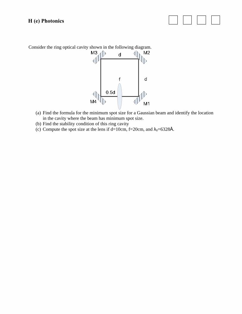
Consider the ring optical cavity shown in the following diagram.
(a) Find the formula for the minimum spot size for a Gaussian beam and identify the location
in the cavity where the beam has minimum spot size. (b) Find the stability condition of this ring cavity (c) Compute the spot size at the lens if d=10cm, f=20cm, and λ0=6328Å.
H (e) Photonics

An optical system that alters the polarization of a plane wave can be described by the Jones matrix. The wave retarders are represented by the following matrix,
.nL 2 where,)exp(0
01retarder wave λ
π Δ=Γ⎥
⎦
⎤⎢⎣
⎡Γ−
=j
T
Find the Jones vectors, ⎟⎟⎠
⎞⎜⎜⎝
⎛⎥⎦
⎤⎢⎣
⎡=
y
x
AA
J
(a)
(b)
450
Half Wave Retarder
xInput
Output
y
H (f) Photonics


![Document Copyrights · • In the receive frequency write mode, the digit being set flashes as it displays the frequency. 2) Pressing [DATA] enables the receive frequency write mode.](https://static.fdocuments.us/doc/165x107/5e6703f88c59a35a546c7429/document-a-in-the-receive-frequency-write-mode-the-digit-being-set-flashes-as.jpg)