Work in Progress --- Not for Publication 1 ERD WG 3/20/09 Brussels IRC FxF Meeting ERD/ERM – IRC...
33
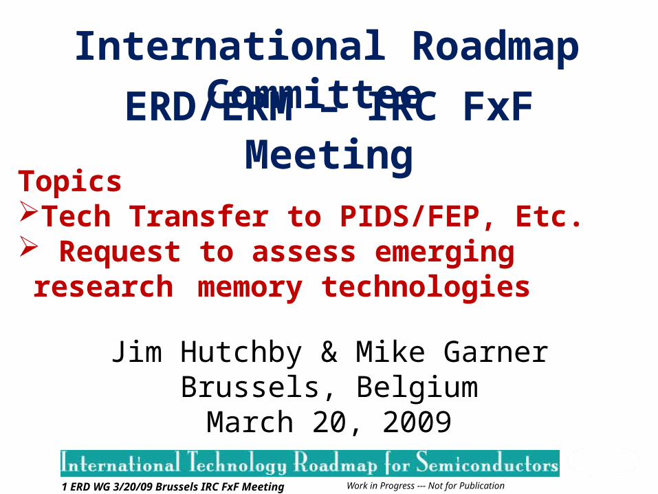
Work in Progress --- Not for Publication 1 ERD WG 3/20/09 Brussels IRC FxF Meeting ERD/ERM – IRC FxF Meeting Jim Hutchby & Mike Garner Brussels, Belgium March 20, 2009 International Roadmap Committee Topics Tech Transfer to PIDS/FEP, Etc. Request to assess emerging research memory technologies
-
Upload
elfrieda-gray -
Category
Documents
-
view
220 -
download
1
Transcript of Work in Progress --- Not for Publication 1 ERD WG 3/20/09 Brussels IRC FxF Meeting ERD/ERM – IRC...
Work in Progress --- Not for Publication1 ERD WG 3/20/09 Brussels IRC FxF Meeting
ERD/ERM – IRC FxF Meeting
Jim Hutchby & Mike GarnerBrussels, BelgiumMarch 20, 2009
International Roadmap Committee
TopicsTech Transfer to PIDS/FEP, Etc. Request to assess emerging research
memory technologies

Work in Progress --- Not for Publication2 ERD WG 3/20/09 Brussels IRC FxF Meeting
Tech Transfer to PIDS/FEP♦ Introduction of technologies involving new materials requires ~12+ years from publication to manufacturing♦ The last 4 – 6 years of this 12+ year total R&D period is development related to PIDS/FEP. The first 6 – 8 years is research related to ERM/ERD.

ITRS 2009 IRC Meeting – March 20, 2009Source: 2009 ITRS – ERD/ERM/PIDS/FEP
Production Ramp-up Model &Technology Cycle Timing for III-V MOSFET Channel Replacement Materials
Vol
ume
(Par
ts/M
onth
)
1K
10K
100K
Months-72
1M
10M
100M
Alpha
Tool
0 24-48
Development Production
Beta
ToolProduct
Tool
First
Conf.
Papers
1st 2Cos.
Reach
Product
Vol
ume
(Waf
ers/
Mon
th)
2
20
200
2K
20K
200K
-24
Research
-96
Transfer to PIDS/FEP(2009–2013)
20192017201520132011 2021

SRC/File name/ 4
TechnologyBackground /Infrastructure
Practicalrealization
1st Practical
useSponsor Entrant
1st
CustomerTelegraph 1801 –
(Voltaic Pile)1823(Schilling)
1844(Morse)
U.S. Gov. 1848 - MagneticTelegraph Co1856- Western Union
Radio 1865 (Maxwell) 1888 (Hertz)1896(Marconi)
1897(Marconi)
BritishPostOffice
1897 WirelessTelegraph&Signal Co
BritishNavy
Vacuumtube
1884(Edison effect)
Fleming (1904)De Forest(1906) - triode
1907 U.S. Navy 1913 - AT&T WW I
1906 AT&T 1907 Pickard Co WW ISolid statediode 1874 (F. Braun) 1900 ( Braun) 1940-
currentRadarProgram
1941 Thomson-Houston1942 AT&T, Sylvania
WWII
Transistor 1923 – 1939 1947-48 1951 AT&T 1951-52 - TI, AT&T,GE, HP. Motorola
DoD
IntegratedCircuit
1944 – 1957(micromoduleprogram)
1958–R.Noyce,J. Kilby
1961 U.S.AirForce
1961 TI, Fairchild NASA,DoD
DataProcessing
1889 Hollerith 1890 U.S.CensusBureau
1896 – TabulatingMachine Co (from1917 – IBM)
U.S.CensusBureau
1946 -Eckert-Mauchly Co(1951 – Remington)
U.S.CensusBureau
Computer 1841(Babbage)
1889Hollerith
1945 - ENIAC 1946-1951 DoD1951 IBM DoD
Disruptive Technologies in Electronics

5
Time Gaps
0
1
2
3
4
5
1870 1880 1890 1900 1910 1920 1930
Transfer of Knowledge
Prototype built (Disruptive Technology)
Entrant Co formed
Market production (Established Technology)
T1~ 20years~10years
T2 T3
Solid State DiodeT1 26 (1874-1900)T2 7 (1900-1907)T3 6 (1907-1913)Learning Period 13 years
Vacuum TubeT1 20 (1884-1904)T2 9 (1904-1913)T3 6 (1913-1919)Learning Period 15 years
TransistorT1 25 (1923-1948)T2 6 (1948-1954)T3 5 (1954-1959)Learning period 11years
Integrated CircuitT1 17 (1942-1959)T2 3 (1959-1961)T3 5(1961-1966)Learning Period 8 years
‘Research Curve’
Human Carrier
Sponsor 1st Customer
Example: Solid State Rectifier
Enabling B
ackground exists

6
Development Cycle Times for Sample IC Technologies
Year Initially Year Implemented LagTool or Technology Developed In Production Time
Silicon Epitaxy 1960-61 1964 4
APCVD Silicon Nitride 1965 1967-68 2
Ion Implant 1969 1973 4
TiW Metalization 1969-70 1975-77 6
Schottky TTL 1970 1974-75 4
Charge-Coupled Device 1970 1981 11
Reactive Ion Etch 1975-76 1980 5
Polysilicon Emitter 1976 1984-85 8
Refractory Gate 1976 1983 7
SOI (via Ion Implant) 1978 1989 11
Trench Capacitor 1979 1986 7
Silicide 1978 1985 7
Lightly-Doped Drain 1980 1986 6
Average 6 years
Source: Graydon Larrabee of Texas Instruments

7
Study of R&D Latency for a few Semiconductor Technologies¨ CMOS¨ Giant Magnetoresistance (GMR)¨ Copper Interconnect¨ 193 nm photoresist¨ Magnetic RAM¨ EUV lithography
Method. We used the following parameters:
1) The first publication on a given technology that appeared in the Science Citation Index database
2) The number of refereed articles in technical journals by year (Science Citation Index database)
3) The year of first production for a given technology

8
CMOS
1
10
100
1000
10000
1965 1970 1975 1980 1985 1990 1995 2000 2005
Year
# of
pub
licat
ions
1969 – 1st publication
1972 – Toshiba CMOS calculator IC
1982 – Intel 80286 CMOS microprocessor
1983 – 1st CMOS DRAM (Intel)
1984 – Motorola 68020 CMOS microprocessor
1987 –CMOS at AMD
1981 – National NSC800 CMOS microprocessor
12 years

9
Giant Magnetoresistance (GMR)
1
10
100
1000
1985 1990 1995 2000 2005
Year
# o
f p
ub
lica
tio
ns
1988 - discovery of GMR effect
1997- 1st hard disk product using GMR heads (IBM)
1992 – MRAM concept
9 years

10
Copper Interconnect
1
10
100
1000
1985 1990 1995 2000 2005
Year
# o
f p
ub
lica
tio
ns
2000 – AMD x86 Cu-based microprocessor
1998 - Power PC 750 microprocessor(IBM)
1986 – 1st publication
12 years

11
193 nm photoresist
1
10
100
1985 1990 1995 2000 2005
Year
# o
f p
ub
lica
tio
ns
2001- 3M debuts 193nm photoresist chemicals
1989 – 1st publication
12 years
12
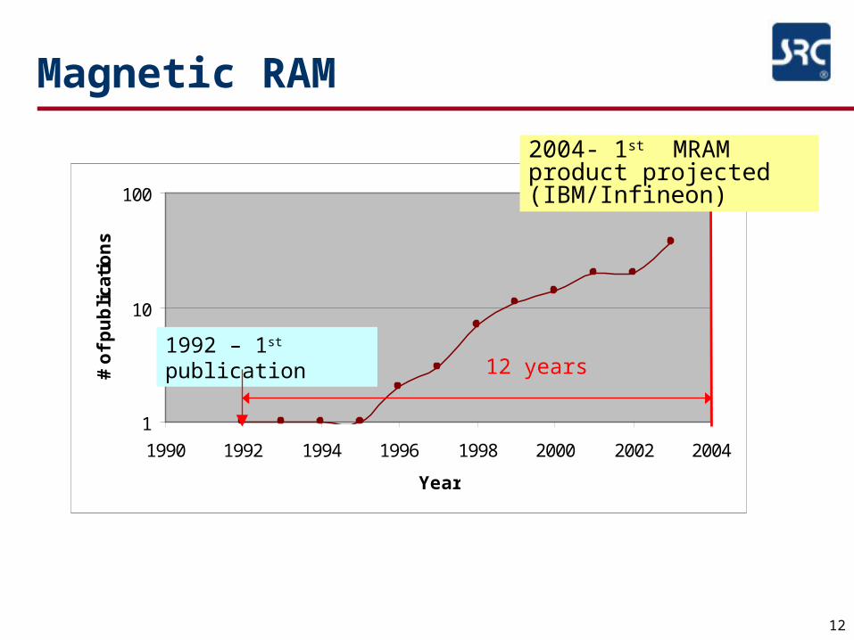
Magnetic RAM
1
10
100
1990 1992 1994 1996 1998 2000 2002 2004
Year
# o
f p
ub
lica
tio
ns
1992 – 1st publication12 years
2004- 1st MRAM product projected (IBM/Infineon)

Work in Progress --- Not for Publication13 ERD WG 3/20/09 Brussels IRC FxF Meeting
New Technology Introduction Events
• Strained Silicon Example– First Technology Paper:
1991, 1994– Addition to ITRS
Roadmap: ~2001– Alpha Tool: TBD– ITRS Production: 2003
(12 years)– Technology Life: 3+
Generations
• High κ (HfO2) Example– First Technology Paper:
1972– Industry Interest ~1990– Addition to ITRS
Roadmap: 1997– Alpha Tool: TBD– ITRS Production: 2010
(38 years)– Technology Life: 3+
Generations

Beyond CMOS CTSG Feb. 3, 2009 Work in Progress: Not for Distribution14
Conclusions
The average time from first research paper on a technology typically using a new material to its’ first commercial production is about 12 years.♦ Research must have been in progress at least a few
years before the first publication♦ Development of technology leading to first product is
4 – 6 years, based on the time gaps study [(T2+T3)/(T1+T2+t3) = 1/3 to 1/2] applied to the current study.

Work in Progress --- Not for Publication15 ERD WG 3/20/09 Brussels IRC FxF Meeting
ERD ITWG Emerging Research Devices
Working Group
Proposal for Assessing Technology Options for Emerging
Research Memory Devices
Jim Hutchby & Mike Garner Friday March 20, 2009

Work in Progress --- Not for Publication16 ERD WG 3/20/09 Brussels IRC FxF Meeting
Objective of IRC/ERD/ERM discussion of this request from Samsung, Hynix, and Micron
ERD/ERM is seeking IRC guidance on whether we should conduct a review and assessment of emerging research memory technologies with the goal of recommending those most promising for detailed roadmapping and accelerated research.♦ Assess technology capability of being scaled beyond the
15nm node.♦ Identify precompetitive research required for top
candidates to scale beyond the 15nm node♦ Process will be completed in April 2010 with an oral report
to the IRC in the Spring ITRS Meeting followed by a written report/recommendation to the IRC.
Work in Progress --- Not for Publication17 ERD WG 3/20/09 Brussels IRC FxF Meeting
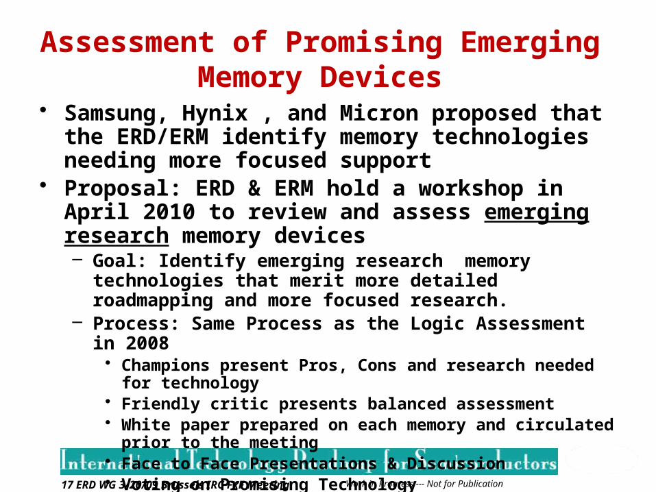
Assessment of Promising Emerging Memory Devices
• Samsung, Hynix , and Micron proposed that the ERD/ERM identify memory technologies needing more focused support
• Proposal: ERD & ERM hold a workshop in April 2010 to review and assess emerging research memory devices– Goal: Identify emerging research memory technologies that merit
more detailed roadmapping and more focused research.– Process: Same Process as the Logic Assessment in 2008
• Champions present Pros, Cons and research needed for technology• Friendly critic presents balanced assessment• White paper prepared on each memory and circulated prior to the
meeting• Face to Face Presentations & Discussion• Voting on Promising Technology• Identify Critical Research Needed

Work in Progress --- Not for Publication18 ERD WG 2/26/2009
Straw Candidate Emerging Research Memory Technologies
Capacitive Memory FeFET Memory
Resistive Memory Nanoelectromechanical STT MRAM Thermal PCM
FUSE/Anti-FUSE Nanowire PCM
Electrochemical Memory Cation migration Anion migration
Electronic Effects Memory Charge trapping Mott Transition FE barrier effects
Macromolecular Memory Molecular Memory

Work in Progress --- Not for Publication19 ERD WG 2/26/2009
DRAFT GOALWith the goal of providing input to resource allocation decisions, ERD/ERM WGs will conduct an in-depth review and assessment of specific emerging research memory devices to highlight the most promising device technologies for detailed roadmapping and acceleration of pre-competitive*research and development.
(*Pre-competitive refers to those technologies capable of being scaled beyond the 15nm node.)

Work in Progress --- Not for Publication20 ERD WG 2/26/2009
DRAFT SCOPE
The scope of the review of emerging research memory technologies will assess scalability beyond the 15nm node. – Identify precompetitive research needed to enable
scaling beyond the 15nm node.– Assessment will encompass both stand-alone and,
where different, embedded emerging research memory technologies.

Work in Progress --- Not for Publication21 ERD WG 2/26/2009
Draft Timetable1. Develop/decide process, milestones, timeline July 12, 2009
2. Develop invitation to advocates/proponents & friendly critics Introduction Potential of technology – fundamental limits Barriers – Fundamental vs. technological/engineering Evaluation Criteria Definition of specific emerging research memory devices for roadmapping Readiness in 10 - 15 years
July 31
3. Identify Major emerging research memory device candidates Strong technical proponent and friendly critic teams and their leaders Knowledgeable ERD/ERM mentor for each proponent team Key questions to be addressed by the teams Background materials for each technical candidate
July 31
4. Issue invitations to team leaders, friendly critics, and ERD/ERM mentors and obtain their commitments
Sept. 15
5. Obtain a white per & background materials from each candidate technology proponent team for ERD/ERM WG review
Jan. 15, 2010
6. ERD/ERM WG review candidate emerging research memory devices candidates based on white papers & identify key questions using a formal process prior to Spring Europe FxF meeting.
Mar. 15, 2010
7. Conduct a FxF review of categories with each proponent & friendly critic making a presentation
April yy, 2010Spring FXF Mtg.
8. On second day of ERD FxF meeting, discuss/decide ERD/ERM WG’s prioritized recommendation of narrowed emerging research memory devices options. This will include selection of specific devices for roadmapping within the recommended option
April yy+1,2010Spring FXF Mtg.
9. Write & submit report on ERD/ERM WG’s recommendations May 31, 2010
Work in Progress --- Not for Publication22 ERD WG 3/20/09 Brussels IRC FxF Meeting
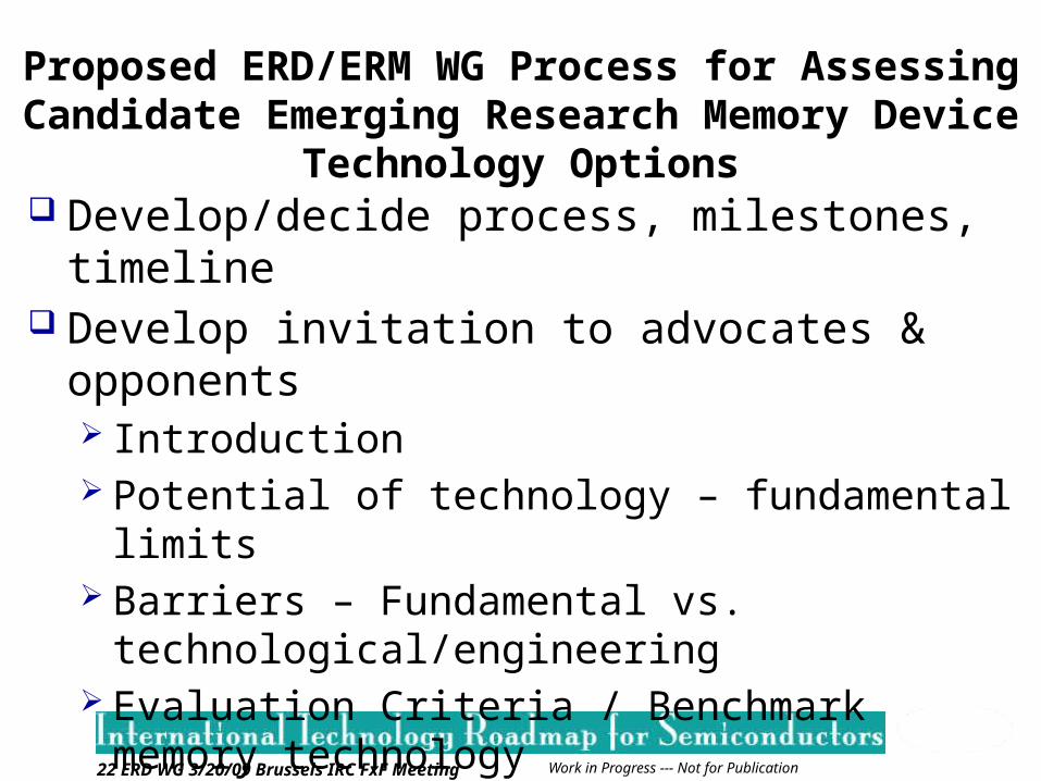
Proposed ERD/ERM WG Process for Assessing Candidate Emerging Research Memory Device Technology Options
Develop/decide process, milestones, timeline Develop invitation to advocates & opponents
Introduction Potential of technology – fundamental limits Barriers – Fundamental vs. technological/engineering Evaluation Criteria / Benchmark memory technology Definition of maturing, high potential specific devices
for roadmapping Readiness in ~ 5 - 10 years

Work in Progress --- Not for Publication23 ERD WG 3/20/09 Brussels IRC FxF Meeting
Proposed ERD/ERM WG Process for Assessing Candidate Emerging Research Memory Device Technology Options
Identify Major emerging research memory technology candidates Strong technical proponent and opponent teams and their
leaders Knowledgeable ERD/ERM mentor for each proponent
team Key questions to be addressed by the teams Background materials for each technical candidate
Issue invitations to team leaders and obtain their commitments
Obtain a white paper & background materials from each candidate technology proponent team for ERD/ERM review

Work in Progress --- Not for Publication24 ERD WG 2/26/2009
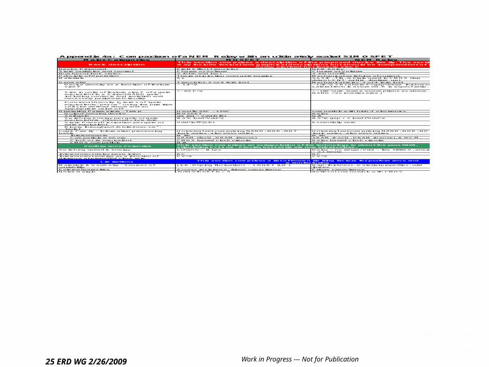
Appendix 4a: Comparison of a NEM Relay with an ultimately scaled Si MOSFET Major Categories MOSFET NEM Relay
Basic description
Device Proposed Field Effect Transistor NEM RelayState variables and control Charge or Voltage Charge or Voltage
Number of logic states 2 (high and low) 2 (on or off)Principle of Operation Thermal injection over gate barrier Mechanical switching of currentMaterials Si Si, SiC, TiN, metals used in CMOS (top
down); CNT or NW (bottom up)Geometry Transistor, 3 or 4 terminal Mechanical relay: 3 or 4 terminal
Device density as a function of feature size F
~ 1/F^2 ~1/(F^2 x R) where F=gap=beam thickness. Lateral tech is assumed. R is aspect ratio.
Size in units of feature size F of a gate equivalent to a 2-input NAND gate, including contacts and isolation and necessary peripheral circuitry
>~65 F^2 >~10F^2xR (same assumptions as above , NAND =2x inverter area.)
Functonal Density in terms of "gate
equivalents" per cm2 using the primitive cell size defined above and an appropriate value of F.
Operating Parameters - Temp Usually 25C - 125C compatible with high-T electronicsOutput sensing device MOSFET RelaySelf gain gm/gd ~ Vdd/DIBL N/ASwitching Energy per gate or gate equivalent @ proposed clock rate
0.5*Cload*Vdd^2 0.5*(Cgap + Cload)*Vdd^2
Static Power Dissipation per gate or gate equivalent
Vdd*Ioff*(2/5) Essentially zero
Binary throughput (Gbits/nsec-cm2-joule)
Logic Family - Information processing basis
Universal set comprising NAND, NOR, NOT logic gates, also pass gates
Universal set comprising NAND, NOR, NOT logic gates, also pass gates
Interconnects Wire WireCompatible memory SRAM (fast) , DRAM (dense) SRAM (Fast) , DRAM (Dense), & NV M.
Clock or its equivalent CMOS based clock circuits Relay based clock circuitsCMOS compatible N/A Yes
Performance Potential
Switching speed & energy Lchan/v ~ 0.1ps Delay ~ ns range; Vdd ~ few 100mV, energy ~ aJ range
Interconnect delay per micron RC RCInterconnect energy as a function of distance at proposed clock rate
CV^2 CV^2
Limitations
Materials & Geometry - Sources of variability
LER, Doping fluctuations ~ 1/SQRT (LW) Gap, thickness, material properties, vdW forces
External parasitics Access resistance, fringe capacitance Fringe capacitanceNoise margin (Vdd-Vth)/ KT/q > 5 Better or comparable with CMOS
This section comprises a description of the proposed device family. The section may include textual and graphical descriptions but should be independent of (or
parameterized by) feature size F
This section comprises a list of known limiting factors for performance and manufacturing
This section comprises an extrapolation of the technology to about the year 2020, stipulating F=14 nm. Provide best estimate numerical values.
REDO THIS
SLID
E
Work in Progress --- Not for Publication25 ERD WG 2/26/2009
Appendix 4a: Comparison of a NEM Relay with an ultimately scaled Si MOSFET Major Categories MOSFET NEM Relay
Basic description
Device Proposed Field Effect Transistor NEM RelayState variables and control Charge or Voltage Charge or Voltage
Number of logic states 2 (high and low) 2 (on or off)Principle of Operation Thermal injection over gate barrier Mechanical switching of currentMaterials Si Si, SiC, TiN, metals used in CMOS (top
down); CNT or NW (bottom up)Geometry Transistor, 3 or 4 terminal Mechanical relay: 3 or 4 terminal
Device density as a function of feature size F
~ 1/F^2 ~1/(F^2 x R) where F=gap=beam thickness. Lateral tech is assumed. R is aspect ratio.
Size in units of feature size F of a gate equivalent to a 2-input NAND gate, including contacts and isolation and necessary peripheral circuitry
>~65 F^2 >~10F^2xR (same assumptions as above , NAND =2x inverter area.)
Functonal Density in terms of "gate
equivalents" per cm2 using the primitive cell size defined above and an appropriate value of F.
Operating Parameters - Temp Usually 25C - 125C compatible with high-T electronicsOutput sensing device MOSFET RelaySelf gain gm/gd ~ Vdd/DIBL N/ASwitching Energy per gate or gate equivalent @ proposed clock rate
0.5*Cload*Vdd^2 0.5*(Cgap + Cload)*Vdd^2
Static Power Dissipation per gate or gate equivalent
Vdd*Ioff*(2/5) Essentially zero
Binary throughput (Gbits/nsec-cm2-joule)
Logic Family - Information processing basis
Universal set comprising NAND, NOR, NOT logic gates, also pass gates
Universal set comprising NAND, NOR, NOT logic gates, also pass gates
Interconnects Wire WireCompatible memory SRAM (fast) , DRAM (dense) SRAM (Fast) , DRAM (Dense), & NV M.
Clock or its equivalent CMOS based clock circuits Relay based clock circuitsCMOS compatible N/A Yes
Performance Potential
Switching speed & energy Lchan/v ~ 0.1ps Delay ~ ns range; Vdd ~ few 100mV, energy ~ aJ range
Interconnect delay per micron RC RCInterconnect energy as a function of distance at proposed clock rate
CV^2 CV^2
Limitations
Materials & Geometry - Sources of variability
LER, Doping fluctuations ~ 1/SQRT (LW) Gap, thickness, material properties, vdW forces
External parasitics Access resistance, fringe capacitance Fringe capacitanceNoise margin (Vdd-Vth)/ KT/q > 5 Better or comparable with CMOS
This section comprises a description of the proposed device family. The section may include textual and graphical descriptions but should be independent of (or
parameterized by) feature size F
This section comprises a list of known limiting factors for performance and manufacturing
This section comprises an extrapolation of the technology to about the year 2020, stipulating F=14 nm. Provide best estimate numerical values.

Work in Progress --- Not for Publication26 ERD WG 3/20/09 Brussels IRC FxF Meeting
Proposed ERD/ERM WG Process for Assessing Candidate Emerging Research Memory Device Technology Options
ERD/ERM WG rate and prioritize candidate emerging research memory technologies using a formal process prior to FxF meeting.
Conduct a FxF review of categories with each proponent & opponent team making a presentation
On second day of ERD/ERM FxF meeting, discuss/decide ERD/ERM’s recommendation of most promising emerging research memory technology options.
Write & submit report to the IRC on ERD/ERM WG’s recommendations

Work in Progress --- Not for Publication27 ERD WG 2/26/2009
BACKGROUND SLIDES

Work in Progress --- Not for Publication28 ERD WG 2/26/2009
Proposed ERD/ERM WG Process for Assessing Candidate Emerging Research Memory Device Technology Options
Develop/decide process, milestones, timeline Identify
Major memory technology candidates Strong technical proponent and friendly critic teams and
their leaders Knowledgeable ERD/ERM mentor for each proponent team Key questions to be addressed by the teams Background materials for each technical candidate
Develop invitation to proponents & friendly criticsIntroductionPotential of technology – fundamental limitsBarriers – Fundamental vs. technological/engineeringEvaluation CriteriaDefinition of specific devices for roadmappingReadiness in 10-15 years

Work in Progress --- Not for Publication29 ERD WG 2/26/2009
Proposed ERD/ERM WG Process for Assessing Candidate Emerging Research Memory Device Technology Options
Issue invitations to proponent and friendly critic team leaders and obtain their commitments
Identify ERD/ERM Mentors – 1 per candidate memory technology
Obtain a white paper & background materials from each candidate technology proponent team for ERD/ERM review
ERD/ERM WG review candidate emerging research memory technologies using a formal process prior to FxF meeting to identify questions to be addressed in FxF meeting.

Work in Progress --- Not for Publication30 ERD WG 2/26/2009
Proposed ERD/ERM WG Process for Assessing Candidate Emerging Research Memory Device Technology Options
Conduct a FxF review of categories with each proponent & friendly critic team making a presentation
On second day of ERD/ERM FxF meeting, discuss/decide ERD/ERM’s recommendation of most promising emerging research memory technology options. Mentors will lead the discussion of their candidate technology
Write & submit report to the IRC on ERD/ERM WG’s recommendations

Work in Progress --- Not for Publication31 ERD WG 2/26/2009
Decision Making & Majority Voting Scheme Each member of ERD WG will be given a maximum of X votes to use
in voting for their top X choices among the candidate technologies (Majority Voting scheme) ERD/ERM WG members present in the FIRST DAY Workshop &
the SECOND DAY meeting will be eligible to vote at SECOND DAY meeting, based on their personal technical judgment, independent of their corporate affiliation or regional representation,
Only 0 or 1 vote can be cast for any candidate technology Member does not have to use all X votes, but cannot use more
than X votes. All members can participate in the straw vote.
The Candidate Technologies will be ordered according to which received the largest number of votes.
Consensus approval will be our goal, but a 75% affirmative vote will be required as a minimum. This is what is meant by the term approximate consensus.
REDO THIS
SLID
E

Work in Progress --- Not for Publication32 ERD WG 2/26/2009
ERD “Beyond CMOS” Technology Selection MtgAgenda – SECOND DAY
9:20 Review Process for selecting beyond CMOS emerging technologies
9:45 Discuss Technologies 9:45 NEMS Switch Technology
10:05 Spin Torque Transfer Technology 10:25 Carbon-based Nanoelectronics
10:45 Break11:00 Atomic Switch / Electrochemical Metal Switch
11:20 Collective Spin Devices (including M-QCA) 11:40 Single Electron Transistors 12:00 CMOL and FPNIREDO T
HIS S
LIDE

Work in Progress --- Not for Publication33 ERD WG 2/26/2009
ERD “Beyond CMOS” Technology Selection Mtg Agenda – SECOND DAY (Cont’d)
12:50 Preliminary vote on technologies – Majority voting process
1:00 Discuss preliminary results
1:45 Second vote on technologies
2:00 Discuss the leading technologies resulting from vote
2:30 Final vote on the leading technology(ies) to determine if we have approximate consensus (75% of those voting) to recommend one or more for roadmapping and enhanced engineering development
2:45 Decide next steps in roadmapping the chosen technologies REDO T
HIS S
LIDE