Wolfgang Porod, -...
54
Jožef Stefan Institute ● Ljubljana, Slovenia ● 20 September 2011 NanoMagnet Logic Wolfgang Porod, Center for Nano Science and Technology University of Notre Dame http://www.nd.edu/~ndnano
Transcript of Wolfgang Porod, -...

Jožef Stefan Institute ● Ljubljana, Slovenia ● 20 September 2011
NanoMagnet Logic
Wolfgang Porod,
Center for Nano Science and Technology
University of Notre Dame
http://www.nd.edu/~ndnano

Alan Seabaugh 2
University of Notre Dame


STINSON REMICK HALL MULTIDISCIPLANARY
TEACHING AND RESEARCH BUILDING

STINSON REMICK HALL MULTIDISCIPLANARY TEACHING AND
RESEARCH BUILDING
• 160,000 Gross square feet, 91,000 Net assignable square feet (NASF)
• One lower level and three levels at and above grade
• LEED Platinum Certification planned
• $69M Total cost
– $1M grant from the Department of Energy
– $68M raised through private donations with significant gifts from the Stinson, Remick, and McCourtney families

STINSON REMICK HALL MULTIDISCIPLANARY TEACHING AND RESEARCH
BUILDING
Nano Science and Technology Center • Home to NDnano and MIND

STINSON REMICK HALL MULTIDISCIPLANARY TEACHING AND RESEARCH
BUILDING
Nano Science and Technology Center • Home to NDnano and MIND
• NDNF has three sections in its clean room, a 1,227 square foot Class 10,000 bay, a 2,336 square foot Class 1,000 bay, and a 2,700 square foot Class 100 bay.

STINSON REMICK HALL MULTIDISCIPLANARY TEACHING AND RESEARCH
BUILDING
Nano Science and Technology Center
Notre Dame and Indiana’s grant to MIND have provided over $10M of new research tools to the
Nano Science and Technology Center
Vistec 5200
EBEAM
$3.1M

Material Characterization facility • Electron Optics Suite on Lower Level
• Notre Dame has invested $7M in state of the art imaging tools from FEI
• Only location with all 3 top of the line FEI tools
• Will be a FEI customer visiting site
Magellan 400 FESEM
Helios Dual
Beam FIB
Titan TEM
STINSON REMICK HALL MULTIDISCIPLANARY TEACHING AND RESEARCH
BUILDING

November 14, 2005 © 2005 IBM Corporation
Xbox 360® CPU Chip Overview 3-Way Symmetric Multi-
Processor
– IBM PowerPC Architecture®
– Specialized Function VMX
– 3.2GHz
Shared 1 MByte L2
Front Side Bus / PHY – 21.6
GB/sec
Phase Locked Loops
– 2 (if,hf) for core clocks
– 2 (if,hf) for PHY clock
Test/control functions
Debug / Trace / performance
monitor
Manufacturing fuses
redundancy, voltage, …
MISC IO
– JTAG, POST, VID, SPI
165 M Transistors
IBM CMOS 10KE – 90nm SOI
CPU CPU
CPU
XBAR
L2
FS
B
PH
Y
TE
ST
/ D
EB
UG
MIS
C IO
PLL
DEBUG IO

Heat Dissipation is the Problem
12

and it has happened before…..
Heat Dissipation is the Problem
13
Year of Announcement
1950 1960 1970 1980 1990 2000 2010
Module
Heat F
lux(w
att
s/c
m2)
0
2
4
6
8
10
12
14
Bipolar
CMOS
?
SRC-NRI goal: develop next device/paradigm
to enable continued growth of electronics
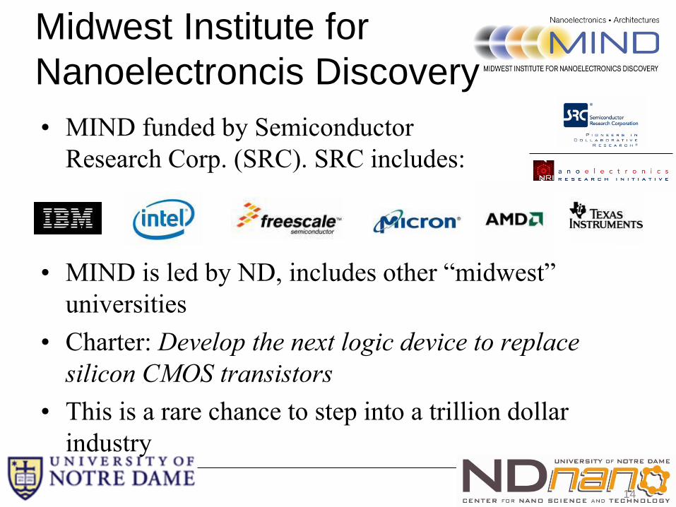
• MIND funded by Semiconductor
Research Corp. (SRC). SRC includes:
• MIND is led by ND, includes other “midwest”
universities
• Charter: Develop the next logic device to replace
silicon CMOS transistors
• This is a rare chance to step into a trillion dollar
industry
14
Midwest Institute for
Nanoelectroncis Discovery

15
NRI-funded universities Finding the next switch
UC Los Angeles
UC Berkeley
UC Irvine
UC Santa
Barbara
Stanford
U Denver
Portland State
U Iowa
Notre Dame Purdue
Illinois-UC Penn State
Michigan UT-Dallas
Cornell GIT
UT-Austin Rice Texas A&M
UT-Dallas ASU Notre Dame
U. Maryland NCSU Illinois UC
Columbia
Harvard
Purdue
UVA
Yale
UC Santa Barbara
Stanford
Notre Dame
U. Nebraska/Lincoln
U. Maryland
Cornell
Illinois UC
Caltech
UC Berkeley
MIT
Northwestern
Brown
U Alabama
SUNY-Albany GIT
Harvard
Purdue RPI Columbia
Caltech MIT NCSU
Yale UVA 30 universities
in 20 states
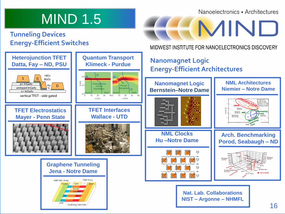
Tunneling Devices Energy-Efficient Switches
16
MIND 1.5
Quantum Transport
Klimeck - Purdue
Heterojunction TFET
Datta, Fay – ND, PSU
TFET Electrostatics
Mayer - Penn State
TFET Interfaces
Wallace - UTD
Graphene Tunneling
Jena - Notre Dame
NML Architectures
Niemier – Notre Dame Nanomagnet Logic
Bernstein–Notre Dame
NML Clocks
Hu –Notre Dame
Nat. Lab. Collaborations
NIST – Argonne – NHMFL
Arch. Benchmarking
Porod, Seabaugh – ND
Nanomagnet Logic Energy-Efficient Architectures
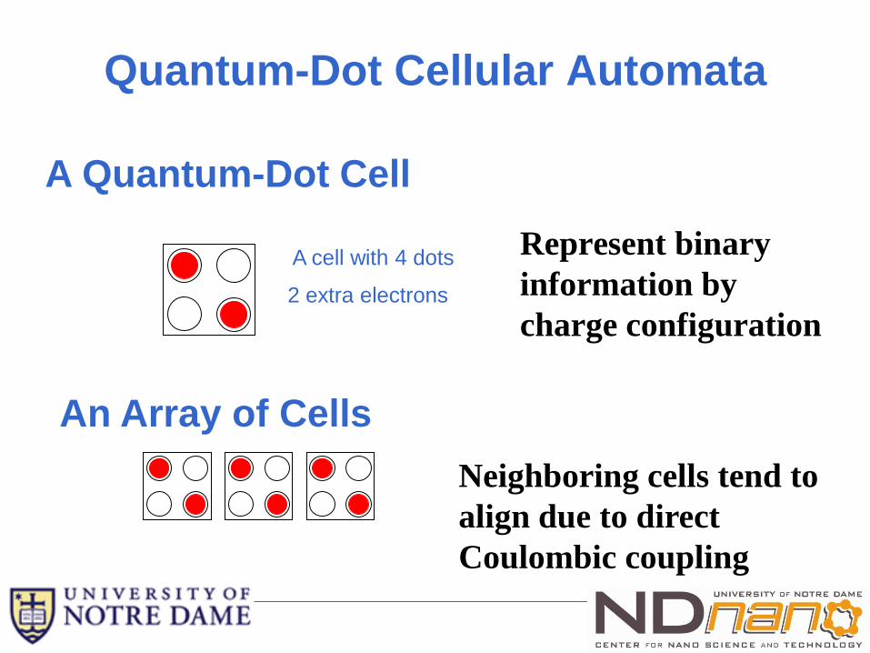
Quantum-Dot Cellular Automata
Represent binary
information by
charge configuration
A cell with 4 dots
2 extra electrons
Neighboring cells tend to
align due to direct
Coulombic coupling
A Quantum-Dot Cell
An Array of Cells

1 1 -1 -1
A
B
C
Out
-1 1 1 -1
Binary wire
Inverter Majority gate
M A
B
C
Programmable 2-input
AND or OR gate.
QCA Devices

Prototype QCA Cells and Devices
• Demonstrated 4-dot cell
• Majority Gate
Amlani, A. Orlov, G. Toth, G. H. Bernstein, C. S.
Lent, G. L. Snider, Science 284, pp. 289-291 (1999).

From metal-dot to molecular QCA
“dot” = metal island 70 mK
Mixed valence compounds
“dot” = redox center
Metal-dot QCA established proof-of-principle.
but …low T, fabrication variations
Molecular QCA: room temp, synthetic consistency
room temperature+
Metal tunnel junctions
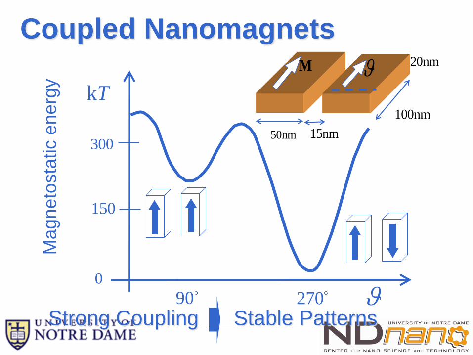
Mag
ne
tosta
tic e
nerg
y
0
150
300
kT
nm20
nm100
nm50 15nm
M
90 270
Coupled Nanomagnets
Strong Coupling Stable Patterns

Gary H. Bernstein, Alexandra Imre, Zhou Ling, George Csaba
Coupled Nanomagnets
Atomic-Force and
Magnetic-Force
Microscopy
(AFM and MFM)

Fabrication and measurement
Electron-beam lithography and lift-off
Magnetic Force Microscopy
~1 micron
AFM MFM
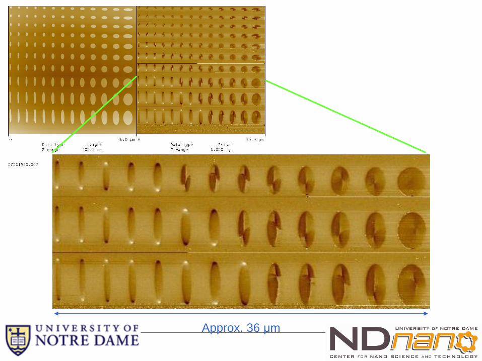
Approx. 36 µm
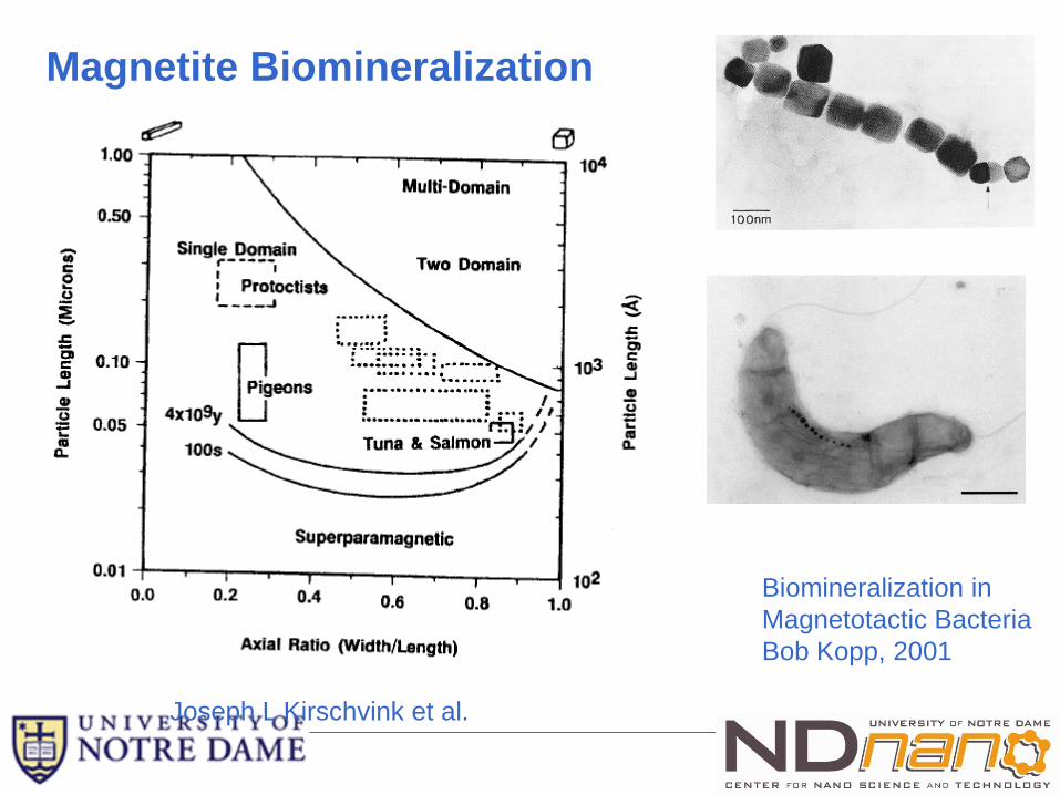
Biomineralization in
Magnetotactic Bacteria
Bob Kopp, 2001
Joseph L Kirschvink et al.
Magnetite Biomineralization
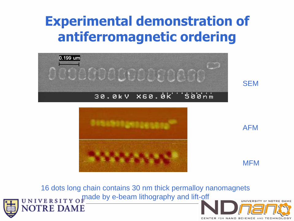
Experimental demonstration of antiferromagnetic ordering
16 dots long chain contains 30 nm thick permalloy nanomagnets
made by e-beam lithography and lift-off
SEM
AFM
MFM

Experimental demonstration of ferromagnetic ordering with input
16 dots long chain contains 30 nm thick permalloy nanomagnets
made by EBL and lift-off
AFM MFM
H

Majority gate geometry
M.C.B. Parish and M. Forshaw,
APPL. PHYS. LETT. 83, 2046 (2003)
A different version off the majority “cross” geometry was proposed by

Demonstration of majority gate operation
A. Imre et al, SCIENCE, VOL. 311, 205 (2006)
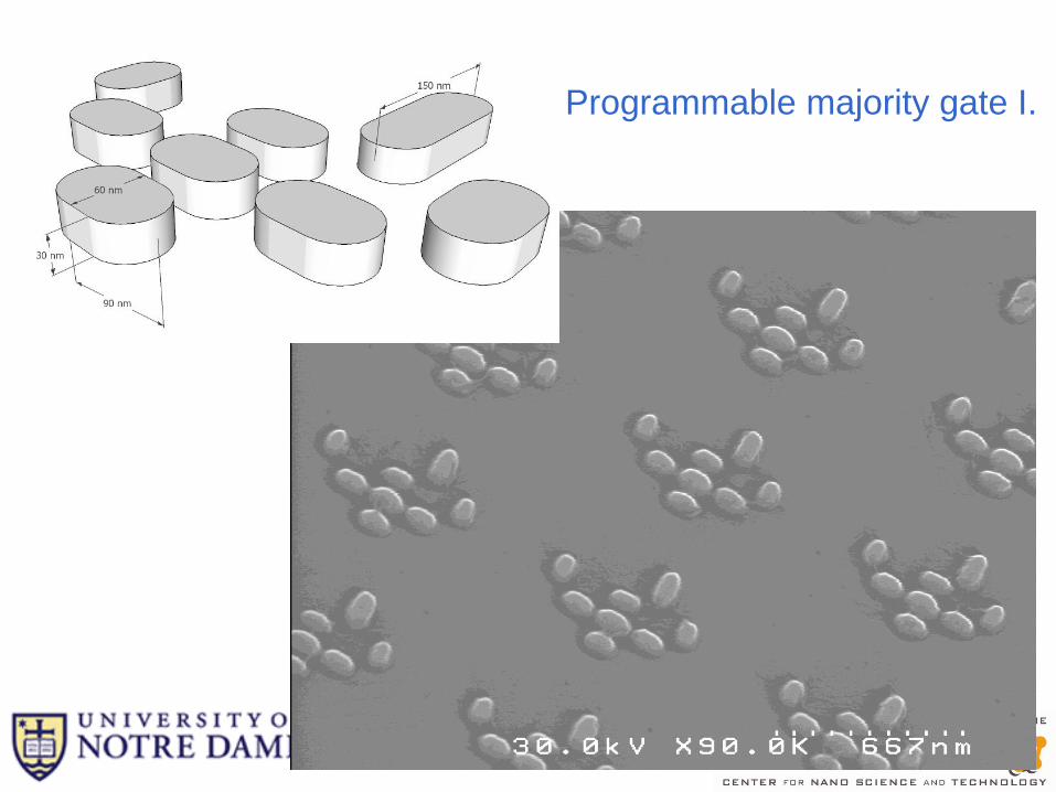
Programmable majority gate I.
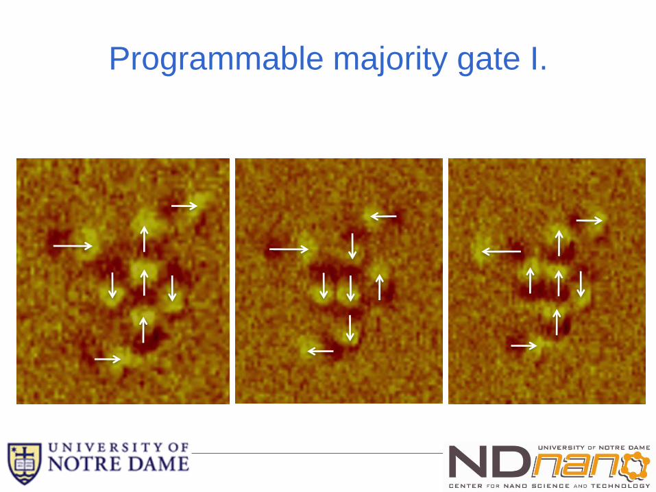
Programmable majority gate I.

Programmable majority gate II.
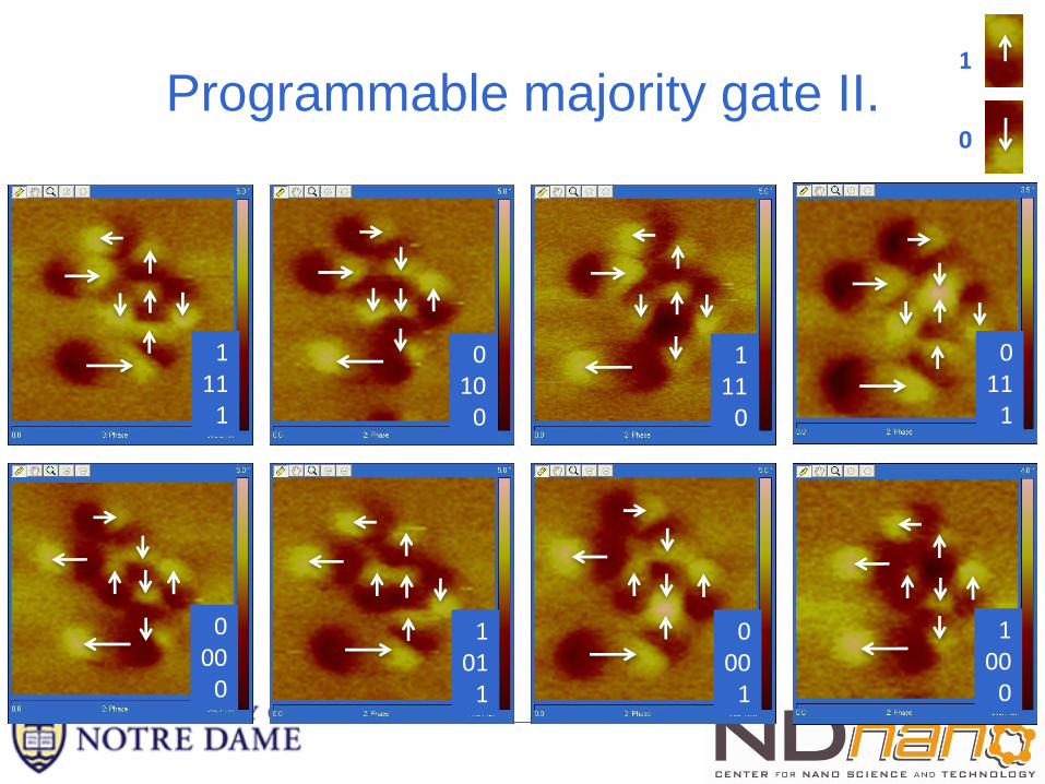
Programmable majority gate II.
11 11 11
10 11 11
11 11 10
10 10 10
11 00 10
10 00 11
11 01 11
10 00 10
1
0

Fanout
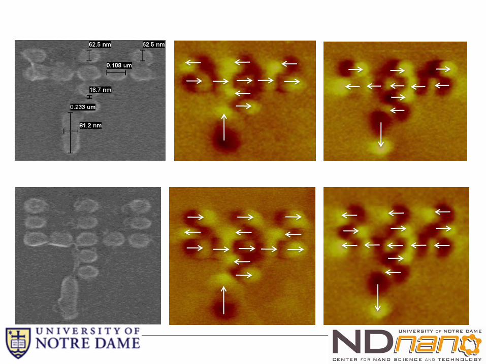

Set#53 array5 H11_c
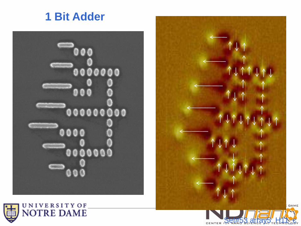
1 Bit Adder
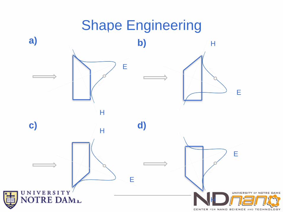
Shape Engineering
E
H
E
H
E
H
E
H a) b)
c) d)

Slant magnets 200 nm
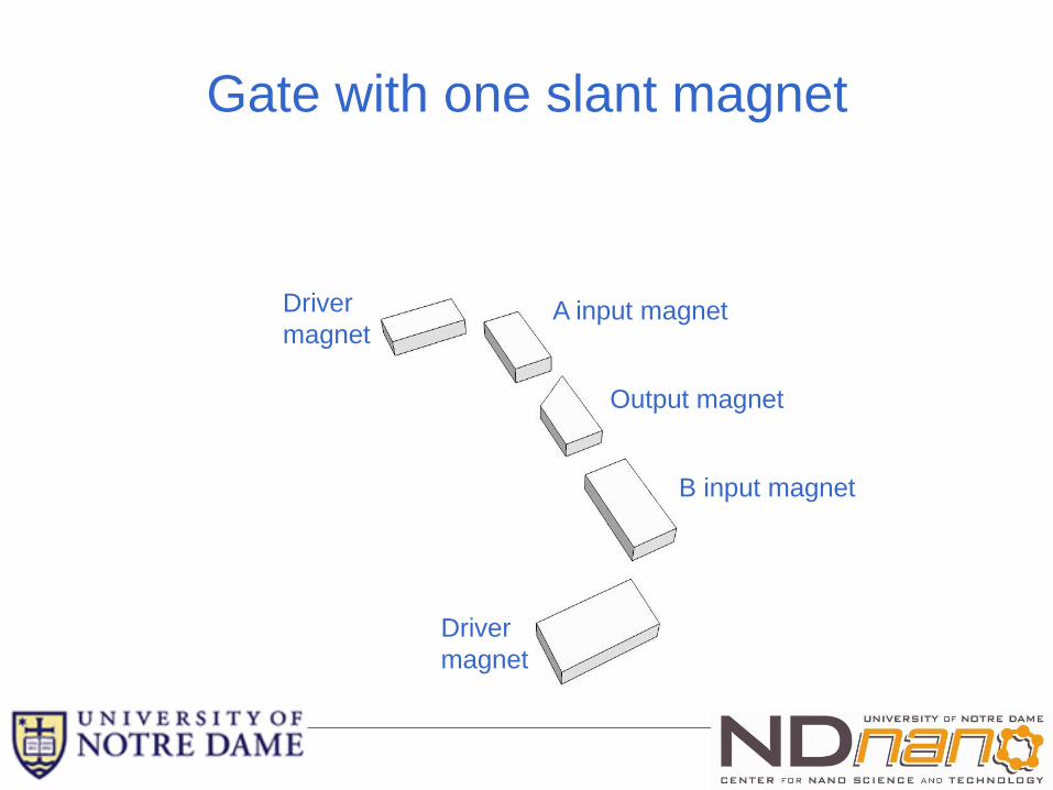
Gate with one slant magnet
Driver
magnet
Driver
magnet
A input magnet
B input magnet
Output magnet

OR AND

NML devices can move, process, and store binary information. They retain state without power, dissipate little energy when switched, and are intrinsically radiation hard.
NML will be used to fabricate a 2-bit adder
In conventional electronic systems, information processing is performed with charge under the influence of electric fields
•Inherent power dissipation associated with the flow of charge leads to unacceptably high levels of heat generation
•Even when devices do not compute, there can be excessive static power
•Computational state is lost when a power supply is turned off
QU
AN
TITA
TIV
E IM
PA
CT
E
ND
-O
F-P
RO
JE
CT
G
OA
L
STA
TU
S Q
UO
N
EW
IN
SIG
HT
S
Nanomagnet Logic (NML)
• Field coupled nanomagnets can represent, move, and process binary information
• Room temperature lines and gates experimentally demonstrated
• Magnets can be controlled, and interface with structures that have been made “on chip”
• The components for the adder– the 5 tenets for a digital system, on-chip clocking, and electrical I/O – have all been experimentally demonstrated.
• We will integrate proven components.
NML devices Clocked devices Spin valves /MTJs
+ +
= Adder Deliverable
Performance Enhancements
• Most of the energy in an NML systems comes from the clock (i.e. mechanism to modulate the device energy barrier)
• 4 enhancement techniques will be studied:
• Enhanced permeability dielectrics
• Multiferroic clocking
• Error correction and analysis techniques will aslo measure, mitigate effects of variation & thermal noise
Extensibility
• Three research threads – CAD, techniques for global interconnect, and techniques for mass manufacture will address large-scale NML systems.
• If 1010 magnets switch 108 times per second, magnets would dissipate just 0.1 W
• 100 aJ add – with I/O, *all* clock circuitry, magnet switching energy can be achieved with components that have already been experimentally demonstrated
• NML is CMOS compatible
• NML is radiation hard
• NML circuits can be reconfigurable
• Develop NML technology to perform circuit operations (with complexity of 2-bit add) with < 10 aJ / operation, 1 ns latencies, with ~ 1mm2 footprints, and 40 kT stability
• Compare NML to 2022 CMOS
• Methodologies for extending NML to larger systems
• Initiate technology transfer
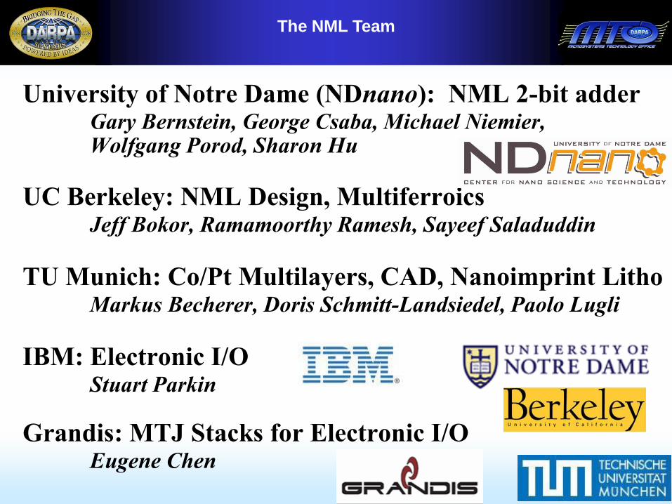
University of Notre Dame (NDnano): NML 2-bit adder Gary Bernstein, George Csaba, Michael Niemier, Wolfgang Porod, Sharon Hu
UC Berkeley: NML Design, Multiferroics Jeff Bokor, Ramamoorthy Ramesh, Sayeef Saladuddin
TU Munich: Co/Pt Multilayers, CAD, Nanoimprint Litho Markus Becherer, Doris Schmitt-Landsiedel, Paolo Lugli
IBM: Electronic I/O Stuart Parkin
Grandis: MTJ Stacks for Electronic I/O Eugene Chen
The NML Team
-SWAN
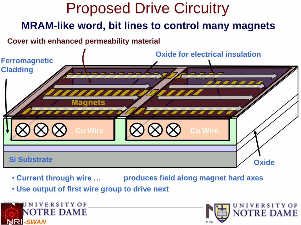
Proposed Drive Circuitry MRAM-like word, bit lines to control many magnets
Oxide Si Substrate
Ferromagnetic
Cladding
Oxide for electrical insulation
Cu Wire Cu Wire
Cover with enhanced permeability material
• Current through wire … produces field along magnet hard axes
• Use output of first wire group to drive next

Clocked NML Devices Demonstrated Nanomagnets patterned on wires
with EBL & lift-off
yo
ke
yo
ke
nanomagnets
Cu
After Excitation 1
Simulations show wire generated fields
can change M state
After Excitation 2
Alam, et. al., “On-chip Clocking for Nanomagnet Logic Devices,” to appear in IEEE Transactions on Nanotechnology
Cladding confines fields - only magnets on wire switch
Yoke
boundary
Yoke
boundary
yoke on-wire off-wire
M. Tanvir Alam
M. Tanvir Alam
First
experiments
used high
current: 600
mA.
Groups of
magnets will
require lower
fields

Input and Output Stack Development 46
Copper Wire
i
iclock line
Cladding
CMOS compatible
clock
Input: Biasing line or
STT
Output: MEI: MTJ, Spin Valve…

Perpendicular Magnetization in Co/Pt Material System
M
Ion beams
Si wafer
Pt 5 nm
Co 0.3 nm
Pt 0.8 nm
Co 0.3 nm
Pt 0.8 nm
}bilayers
Magnetic dots can be fabricated without
removing material from the surface.
Narrow switching field distribution
Possibility to fine-tune magnetic
properties
Prof. Doris Schmitt-Landsiedel, TUM LTE

Technische Universität München
48
Experimental results: Tailoring magnetic properties by FIB irradiation
'High' FIB dose:
'Artificial' domains 'Low' FIB dose:
Tailoring coercivity
* C. Chappert et. al., Science,
1998.

Technische Universität München
49
FIB-Patterning of Co/Pt multilayers
bright: up-state
dark: down-state
Technische Universität München
50
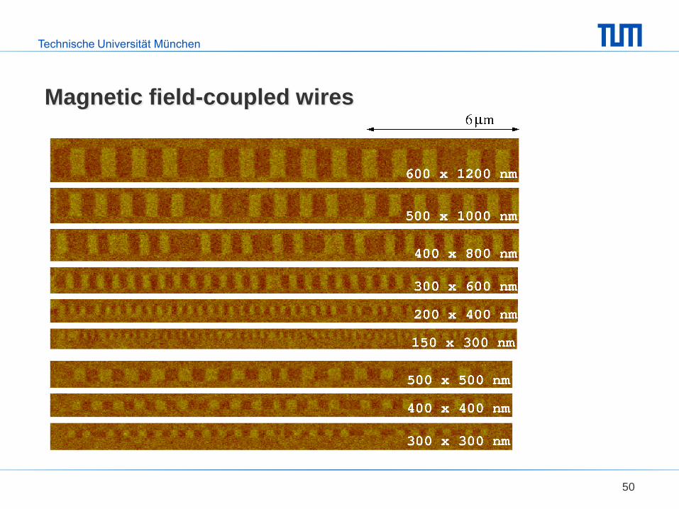
Magnetic field-coupled wires

Technische Universität München
51
Further field-coupled patterns in Co/Pt
Technische Universität München
52
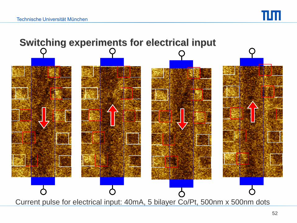
Switching experiments for electrical input
Current pulse for electrical input: 40mA, 5 bilayer Co/Pt, 500nm x 500nm dots

• Experimental Demonstration of Basic Circuit Elements, such as Lines and Logic Gates, and Clocking
• NML Satisfies Basic Requirements
for Digital Logic 1. Nonlinear Device Characteristics 2. Functionally Complete Logic Set 3. Amplification / Gain 4. Directionality of Signal Flow 5. Feedforward / Drive
NML State-of-the-Art

Thanks to … • Magnetic QCA
– Lili Ji, Edit Varga, and Tanvir Alam (NDnano) … Fabrication and MFM
– Alexandra Imre (ANL) … Fabrication and MFM
– George Csaba and Paolo Lugli (TUM) … Theory and Modeling, Nanoimprint
– Markus Becherer and Doris Schmitt-Landsiedel (TUM) … Co/Pt Structures
– Gary Bernstein and Alexei Orlov (NDnano) … Fabrication and Testing
– Michael Niemier and Sharon Hu (NDnano) … Architectures
• Sponsors
– Office of Naval Research
– National Science Foundation
– Semiconductor Research Corporation
– DARPA