WL865E4-P PCB Antenna Integartion Application Note
34
WL865E4-P PCB Antenna Integration Application Note 80613NT11771A Rev 3 – 2019-10-23
Transcript of WL865E4-P PCB Antenna Integartion Application Note

WL865E4-P PCB Antenna Integration Application Note
80613NT11771A Rev 3 – 2019-10-23

WL865E4-P PCB Antenna Integration Application Note
80613NT11771A Rev 3.0 Page 2 of 34 2019-10-23
NOTICE
COPYRIGHTS
COMPUTER SOFTWARE COPYRIGHTS
SPECIFICATIONS ARE SUBJECT TO CHANGE WITHOUT NOTICE
While reasonable efforts have been made to assure the accuracy of this document, Telit assumes no liability resulting from any inaccuracies or omissions in this document, or from use of the information obtained herein. The information in this document has been carefully checked and is believed to be reliable. However, no responsibility is assumed for inaccuracies or omissions. Telit reserves the right to make changes to any products described herein and reserves the right to revise this document and to make changes from time to time in content hereof with no obligation to notify any person of revisions or changes. Telit does not assume any liability arising out of the application or use of any product, software, or circuit described herein; neither does it convey license under its patent rights or the rights of others.
It is possible that this publication may contain references to, or information about Telit products (machines and programs), programming, or services that are not announced in your country. Such references or information must not be construed to mean that Telit intends to announce such Telit products, programming, or services in your country.
This instruction manual and the Telit products described in this instruction manual may be, include or describe copyrighted Telit material, such as computer programs stored in semiconductor memories or other media. Laws in the Italy and other countries preserve for Telit and its licensors certain exclusive rights for copyrighted material, including the exclusive right to copy, reproduce in any form, distribute and make derivative works of the copyrighted material. Accordingly, any copyrighted material of Telit and its licensors contained herein or in the Telit products described in this instruction manual may not be copied, reproduced, distributed, merged or modified in any manner without the express written permission of Telit. Furthermore, the purchase of Telit products shall not be deemed to grant either directly or by implication, estoppel, or otherwise, any license under the copyrights, patents or patent applications of Telit, as arises by operation of law in the sale of a product.
The Telit and 3rd Party supplied Software (SW) products described in this instruction manual may include copyrighted Telit and other 3rd Party supplied computer programs stored in semiconductor memories or other media. Laws in the Italy and other countries preserve for Telit and other 3rd Party supplied SW certain exclusive rights for copyrighted computer programs, including the exclusive right to copy or reproduce in any form the copyrighted computer program. Accordingly, any copyrighted Telit or other 3rd Party supplied SW computer programs contained in the Telit products described in this instruction manual may not be copied (reverse engineered) or reproduced in any manner without the express written permission of Telit or the 3rd Party SW supplier. Furthermore, the purchase of Telit products shall not be deemed to grant either directly or by implication, estoppel, or otherwise, any license under the copyrights, patents or patent applications of Telit or other 3rd Party supplied SW, except for the normal non-exclusive, royalty free license to use that arises by operation of law in the sale of a product.

WL865E4-P PCB Antenna Integration Application Note
80613NT11771A Rev 3.0 Page 3 of 34 2019-10-23
USAGE AND DISCLOSURE RESTRICTIONS
I. License Agreements
II. Copyrighted Materials
III. High Risk Materials
IV. Trademarks
V. Third Party Rights
The software described in this document is the property of Telit and its licensors. It is furnished by express license agreement only and may be used only in accordance with the terms of such an agreement.
Software and documentation are copyrighted materials. Making unauthorized copies is prohibited by law. No part of the software or documentation may be reproduced, transmitted, transcribed, stored in a retrieval system, or translated into any language or computer language, in any form or by any means, without prior written permission of Telit
Components, units, or third-party products used in the product described herein are NOT fault-tolerant and are NOT designed, manufactured, or intended for use as on-line control equipment in the following hazardous environments requiring fail-safe controls: the operation of Nuclear Facilities, Aircraft Navigation or Aircraft Communication Systems, Air Traffic Control, Life Support, or Weapons Systems (High Risk Activities"). Telit and its supplier(s) specifically disclaim any expressed or implied warranty of fitness for such High-Risk Activities.
TELIT and the Stylized T Logo are registered in Trademark Office. All other product or service names are the property of their respective owners.
The software may include Third Party Right software. In this case you agree to comply with all terms and conditions imposed on you in respect of such separate software. In addition to Third Party Terms, the disclaimer of warranty and limitation of liability provisions in this License shall apply to the Third-Party Right software.
TELIT HEREBY DISCLAIMS ANY AND ALL WARRANTIES EXPRESS OR IMPLIED FROM ANY THIRD PARTIES REGARDING ANY SEPARATE FILES, ANY THIRD PARTY MATERIALS INCLUDED IN THE SOFTWARE, ANY THIRD PARTY MATERIALS FROM WHICH THE SOFTWARE IS DERIVED (COLLECTIVELY “OTHER CODE”), AND THE USE OF ANY OR ALL THE OTHER CODE IN CONNECTION WITH THE SOFTWARE, INCLUDING (WITHOUT LIMITATION) ANY WARRANTIES OF SATISFACTORY QUALITY OR FITNESS FOR A PARTICULAR PURPOSE.
NO THIRD PARTY LICENSORS OF OTHER CODE SHALL HAVE ANY LIABILITY FOR ANY DIRECT, INDIRECT, INCIDENTAL, SPECIAL, EXEMPLARY, OR CONSEQUENTIAL DAMAGES (INCLUDING WITHOUT LIMITATION LOST PROFITS), HOWEVER CAUSED AND WHETHER MADE UNDER CONTRACT, TORT OR OTHER LEGAL THEORY, ARISING IN ANY WAY OUT OF THE USE OR DISTRIBUTION OF THE OTHER CODE OR THE EXERCISE OF ANY RIGHTS GRANTED UNDER EITHER OR BOTH THIS LICENSE AND THE LEGAL TERMS APPLICABLE TO ANY SEPARATE FILES, EVEN IF ADVISED OF THE POSSIBILITY OF SUCH DAMAGES.

WL865E4-P PCB Antenna Integration Application Note
80613NT11771A Rev 3.0 Page 4 of 34 2019-10-23
APPLICABILITY TABLE
PRODUCTS
WL865E4-P
Note: The features described in the present document are provided by the products equipped with the software versions equal or higher than the versions shown in the table. See also the Document History chapter.
WL865E4-P PCB Antenna Integration Application Note
80613NT11771A Rev 3.0 Page 5 of 34 2019-10-23
CONTENTS NOTICE………. .............................................................................................. 2
COPYRIGHTS ................................................................................................ 2
COMPUTER SOFTWARE COPYRIGHTS ...................................................... 2
USAGE AND DISCLOSURE RESTRICTIONS ............................................... 3
APPLICABILITY TABLE ................................................................................ 4
CONTENTS .................................................................................................... 5
FIGURE………… ............................................................................................ 7
TABLES…………….. ...................................................................................... 8
1. INTRODUCTION .......................................................................... 9
Overview....................................................................................... 9
Terminology .................................................................................. 9
2. ANTENNA DIMENSION ............................................................. 10
3. MEASUREMENT SETUP ........................................................... 11
4. ANTENNA DESIGN ................................................................... 12
Antenna Design Application ........................................................ 12
Mechanical Data and Consideration ........................................... 12
Electrical (RF) data and considerations ...................................... 12
5. RF PERFORMANCE .................................................................. 13
Wi-Fi ........................................................................................... 13
5.1.1. Return Loss ................................................................................ 13
5.1.2. Wi-Fi Radiation Efficiency and Peak Gain ................................... 14
5.1.3. Radiation Pattern ........................................................................ 15
BT ............................................................................................... 19
5.2.1. Return Loss ................................................................................ 19
5.2.2. BT Radiation Efficiency and peak Gain ....................................... 20
5.2.3. Radiation Pattern ........................................................................ 21
6. ISOLATION BETWEEN WI-FI AND BT ANTENNAS ................. 23
7. ANTENNA PLACEMENT AND INTEGRATION RULES ............ 24
Antenna Placing.......................................................................... 24
Minimal PCB Design ................................................................... 24
7.2.1. Wi-Fi Antenna ............................................................................. 25

WL865E4-P PCB Antenna Integration Application Note
80613NT11771A Rev 3.0 Page 6 of 34 2019-10-23
7.2.2. BT Antenna ................................................................................. 26
8. TRANSMISSION LINE ............................................................... 27
9. MATCHING CIRCUITS ............................................................... 28
10. ANTENNA DESIGN WORKFLOW ............................................. 29
Mechanical Dimension ................................................................ 29
Design Workflow ......................................................................... 30
11. CERTIFICATIONS AND ANTENNA CHANGES ........................ 31
Europe – Radio Equipment Directive .......................................... 31
North America (US - FCC & Canada - ISED) .............................. 32
DOCUMENT HISTORY ................................................................................ 33

WL865E4-P PCB Antenna Integration Application Note
80613NT11771A Rev 3.0 Page 7 of 34 2019-10-23
Figure
Figure 1: Return Loss of the Wi-Fi Antenna .................................................................. 13
Figure 2: Radiated Efficiency and Peak Gain of the Wi-Fi antenna ............................... 14
Figure 3: 3D Radiation Pattern of the Wi-Fi antenna, f = 2440MHz ............................... 15
Figure 4: 3D Radiation Pattern of the Wi-Fi antenna from different cuts, f = 2440MHz .. 16
Figure 5: 3D Radiation Pattern of the Wi-Fi antenna, f = 5500MHz ............................... 17
Figure 6: 3D Radiation Pattern of the Wi-Fi antenna from different cuts, f = 5500MHz .. 18
Figure 7: Return Loss of the BT antenna ...................................................................... 19
Figure 8: Radiated Efficiency and Peak Gain of the BT antenna ................................... 20
Figure 9: 3D Radiation Pattern of the BT antenna, f = 2440MHz ................................... 21
Figure 10: 3D Radiation Pattern of the BT antenna from different cuts, f = 2440MHz.... 22
Figure 11: Isolation between Wi-Fi and BT Antennas .................................................... 23
Figure 12: Dimensions of Two Antenna Components ................................................... 10
Figure 13: Antenna Placement ...................................................................................... 24
Figure 14: Wi-FI PCB .................................................................................................... 25
Figure 15: BT PCB ........................................................................................................ 26
Figure 16: Correct RF Transmission line Area .............................................................. 27
Figure 17: Pi-network .................................................................................................... 28
Figure 18: Wi-Fi Antenna .............................................................................................. 29
Figure 19: BT Antenna .................................................................................................. 29
Figure 20: Antenna Design Workflow ............................................................................ 30

WL865E4-P PCB Antenna Integration Application Note
80613NT11771A Rev 3.0 Page 8 of 34 2019-10-23
Tables
Table 1: Glossary of Terms ............................................................................................. 9
Table 2: Minimal Electrical Performances ..................................................................... 12
Table 3: Electrical Performances of the reference Design ............................................. 12

WL865E4-P PCB Antenna Integration Application Note
80613NT11771A Rev 3.0 Page 9 of 34 2019-10-23
1. INTRODUCTION
This document provides detailed information about WL865E4-P PCB Antenna Integration.
Overview
It demonstrates an example of Wi-Fi and BT PCB antennas integrated for WL865E4-P Telit module. The example has two antennas design - one for 2.4GHz – 5GHz dual band Wi-Fi antenna and another for 2.4GHz single band BT antenna. Practical examples are presented to explain the integration rules.
Terminology
The following table lists the different terminologies used in this document.
Term Explanation
BT Bluetooth
DXF Drawing Exchange Formats
EIRP Effective Isotropic Radiated Power
FR-4 Flame Retardant - 4
NM Not Mount (on PCB)
OTA Over the Air
PCB Printed Circuit Board
RL Return Loss
RF Radio Frequency
Table 1: Glossary of Terms

WL865E4-P PCB Antenna Integration Application Note
80613NT11771A Rev 3.0 Page 10 of 34 2019-10-23
2. ANTENNA DIMENSION
The following figure shows the dimensions of the two antenna components:
Figure 1: Dimensions of Two Antenna Components

WL865E4-P PCB Antenna Integration Application Note
80613NT11771A Rev 3.0 Page 11 of 34 2019-10-23
3. MEASUREMENT SETUP
The following figure shows the OTA measurement set-up of the reference design:
Figure 1: OTA set-up

WL865E4-P PCB Antenna Integration Application Note
80613NT11771A Rev 3.0 Page 12 of 34 2019-10-23
4. ANTENNA DESIGN
The design covers the following frequency bands:
Wi-Fi antenna: 2.4 - 2.5GHz and 4.9-5.9GHz bands
BT antenna: 2.4 - 2.5GHz
Advantages of this design:
• PCB quasi-independent design, zero thickness design
• High efficiency
• High input impedance
Antenna Design Application
It is possible to use this design for every application using the Telit WL865E4-P module. The only restriction is the minimal PCB dimensions to integrate the antennas (see chapter 7 Antenna Placement and Integration Rules).
Mechanical Data and Consideration
The antennas are made with the same material of the PCB: copper and dielectric support with relative dielectric constant of 4.5. The dielectric thickness is 1.6 mm, it is possible to tune the antennas upon different dielectric constant (4.2 +/- 10%) thickness from 1 to 1.6mm and dielectric constant of generic FR4 material.
Electrical (RF) data and considerations
The electrical data would slightly change for every design, due to the material used and the environment around the antenna (metallic object, case of the device etc..).
With the instructions from this guide, the efficiency of both antennas will be greater or in line with any dielectric (ceramic or similar) antenna in the market. The efficiency in both bands greater than 50% (-3dB).
Wi-Fi Antenna BT Antenna
f range [GHz] 2.4 - 2.5 4.9 - 5.9 2.4 - 2.5
EIRP on the edges [dBi] 0 – 3* 0 – 3* 0 – 3*
Efficiency on the edges [dB] > -3 (50%) > -3 (50%) > -3 (50%)
RL on the edges [dB] < -8 < -10 < -10
Table 2: Minimal Electrical Performances
* depends on PCB’s dimension
Wi-Fi Antenna BT Antenna
f range [GHz] 2.4 - 2.5 4.9 - 5.9 2.4 - 2.5
EIRP on the edges [dBi] 1 2 3
Efficiency on the edges [dB] -2.4 (58%) -2.2 (60%) -1.9 (65%)
RL on the edges [dB] -9.3 -9.0 -14.8 -19.8 -18.3 -17.0
Table 3: Electrical Performances of the reference Design

WL865E4-P PCB Antenna Integration Application Note
80613NT11771A Rev 3.0 Page 13 of 34 2019-10-23
5. RF PERFORMANCE
Wi-Fi
5.1.1. Return Loss
Measurements are in Quasi-Free-Space.
Figure 3: Return Loss of the Wi-Fi Antenna
Marker M1-M2 is the low band and marker M3-M4 is the upper band.

WL865E4-P PCB Antenna Integration Application Note
80613NT11771A Rev 3.0 Page 14 of 34 2019-10-23
5.1.2. Wi-Fi Radiation Efficiency and Peak Gain
Figure 4: Radiated Efficiency and Peak Gain of the Wi-Fi antenna
Lower range is 2.4-2.5GHz band, upper range is 4.9-5.9GHz.
Yellow trace is the efficiency, blue trace is the EIRP (radiated power in direction of the maximum [dBi]).

WL865E4-P PCB Antenna Integration Application Note
80613NT11771A Rev 3.0 Page 15 of 34 2019-10-23
5.1.3. Radiation Pattern
5.1.3.1. 2.44GHz
Figure 5: 3D Radiation Pattern of the Wi-Fi antenna, f = 2440MHz

WL865E4-P PCB Antenna Integration Application Note
80613NT11771A Rev 3.0 Page 16 of 34 2019-10-23
Figure 6: 3D Radiation Pattern of the Wi-Fi antenna for different cuts, f = 2440MHz

WL865E4-P PCB Antenna Integration Application Note
80613NT11771A Rev 3.0 Page 17 of 34 2019-10-23
5.1.3.2. 5.5GHz
Figure 7: 3D Radiation Pattern of the Wi-Fi antenna, f = 5500MHz

WL865E4-P PCB Antenna Integration Application Note
80613NT11771A Rev 3.0 Page 18 of 34 2019-10-23
Figure 8: 3D Radiation Pattern of the Wi-Fi antenna for different cuts, f = 5500MHz

WL865E4-P PCB Antenna Integration Application Note
80613NT11771A Rev 3.0 Page 19 of 34 2019-10-23
BT
5.2.1. Return Loss
Figure 9: Return Loss of the BT antenna
Marker M1-M2 is for BT band and marker M3-M4 is for upper Wi-Fi band.

WL865E4-P PCB Antenna Integration Application Note
80613NT11771A Rev 3.0 Page 20 of 34 2019-10-23
5.2.2. BT Radiation Efficiency and peak Gain
Figure 10: Radiated Efficiency and Peak Gain of the BT antenna
Lower range is for the BT 2.4-2.5GHz and upper range is for Wi-Fi band 4.9-5.9GHz.
Yellow trace is the efficiency and blue trace is the EIRP.

WL865E4-P PCB Antenna Integration Application Note
80613NT11771A Rev 3.0 Page 21 of 34 2019-10-23
5.2.3. Radiation Pattern
5.2.3.1. 2.440GHz
Figure 11: 3D Radiation Pattern of the BT antenna, f = 2440MHz

WL865E4-P PCB Antenna Integration Application Note
80613NT11771A Rev 3.0 Page 22 of 34 2019-10-23
Figure 12: 3D Radiation Pattern of the BT antenna for different cuts, f = 2440MHz

WL865E4-P PCB Antenna Integration Application Note
80613NT11771A Rev 3.0 Page 23 of 34 2019-10-23
6. ISOLATION BETWEEN WI-FI AND BT ANTENNAS
Good isolation between Wi-Fi and BT antennas is mandatory. It is strongly recommended to maintain an isolation greater than 12dB between both antennas. Wi-Fi and BT antennas must be well isolated with respect to any other antenna from a different RF transceiver like Cellular, GNSS, etc.
Figure 13: Isolation between Wi-Fi and BT Antennas
M1-M2 is for BT and Wi-Fi lower band while M3-M4 is for Wi-Fi upper band.

WL865E4-P PCB Antenna Integration Application Note
80613NT11771A Rev 3.0 Page 24 of 34 2019-10-23
7. ANTENNA PLACEMENT AND INTEGRATION RULES
Antenna Placing
Good isolation between antennas is -12dB but the value lower than -10dB is acceptable.
Following is the graphical representation of the antenna’s placement goodness.
Figure 14: Antenna Placement
The green rectangle represents the PCB, the two orange small rectangles at the border are the antennas.
A and B are the best options, to place the antennas in your design. C and D are good placing areas, while E and F are NON suggested options.
Minimal PCB Design
For small PCB dimension, it is strongly recommended to choose option A and B in Figure 1: Dimensions of Two Antenna Components
WL865E4-P PCB Antenna Integration Application Note
80613NT11771A Rev 3.0 Page 25 of 34 2019-10-23
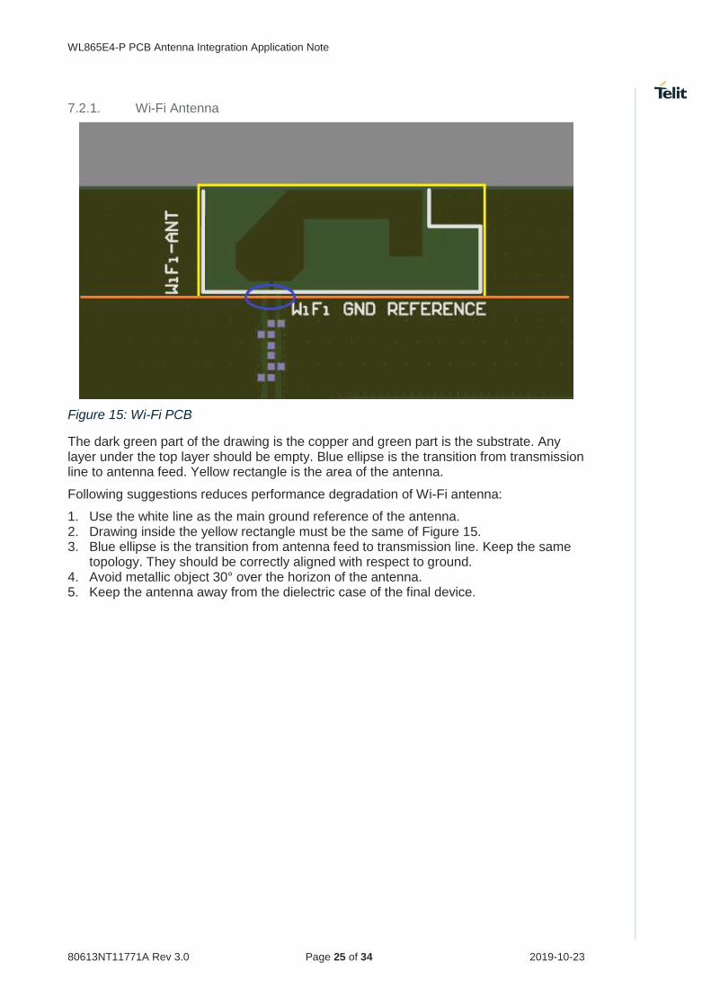
7.2.1. Wi-Fi Antenna
Figure 15: Wi-Fi PCB
The dark green part of the drawing is the copper and green part is the substrate. Any layer under the top layer should be empty. Blue ellipse is the transition from transmission line to antenna feed. Yellow rectangle is the area of the antenna.
Following suggestions reduces performance degradation of Wi-Fi antenna:
1. Use the white line as the main ground reference of the antenna. 2. Drawing inside the yellow rectangle must be the same of Figure 15. 3. Blue ellipse is the transition from antenna feed to transmission line. Keep the same
topology. They should be correctly aligned with respect to ground. 4. Avoid metallic object 30° over the horizon of the antenna. 5. Keep the antenna away from the dielectric case of the final device.

WL865E4-P PCB Antenna Integration Application Note
80613NT11771A Rev 3.0 Page 26 of 34 2019-10-23
7.2.2. BT Antenna
Figure 16: BT PCB
The dark green part of the drawing is the copper and green part is the substrate. Any layer under the top layer should be empty. Blue ellipse is the transition from transmission line to the antenna feed. Yellow rectangle is the area of the antenna.
Following suggestions reduces performance degradation of BT antenna:
1. Use the orange line as the main ground reference of the antenna. 2. Drawing inside the yellow rectangle must be the same of Figure 16. 3. Blue ellipse is the transition from antenna feed to transmission line. Keep the same
topology. They should be correctly aligned with respect to ground. 4. Avoid metallic object 30° over the horizon of the antenna. 5. Keep the antenna away from the dielectric case of the final device.

WL865E4-P PCB Antenna Integration Application Note
80613NT11771A Rev 3.0 Page 27 of 34 2019-10-23
8. TRANSMISSION LINE
The transmission line must be designed with characteristic impedance of 50Ohm. We suggest a width of the transmission line around 0.7mm (same width of the RF pads). The length of the transmission line should be kept minimum.
Pay attention to maintain characteristic impedance of 50Ohm in every section of the transmission line, avoiding 90° angle. To change direction, use smooth curvature, avoiding impedance steps between module’s RF pads and transmission lines and on matching circuits areas.
Once the material of the PCB is chosen, along with PCB thickness and dielectric constant, a grounded coplanar transmission line can be easily designed using any transmission line characteristic impedance calculator.
Figure 17: Correct RF Transmission line Area
Example of correct RF transmission line area where it is possible to observe that the width of the RF pads and the width of the coplanar transmission line are similar, also the change of direction are smooth, avoiding 90° bending. The presence of the many close path helps isolating the transmission line.

WL865E4-P PCB Antenna Integration Application Note
80613NT11771A Rev 3.0 Page 28 of 34 2019-10-23
9. MATCHING CIRCUITS
This antenna design works without a matching network. If space is not a problem, then we suggest the insertion of a π type matching network circuitry for both Wi-Fi and BT antennas. The reference circuits are: Shunt NM – Shunt NM – 0 Ohm series - Shunt NM – Shunt NM. If necessary, this circuitry will be used during final antenna impedance tuning process.
Following is the representation of the matching π -network:
Figure 18: π -network
The transition between the transmission line and matching network must not perturbe the characteristic impedance of the transmission line.

WL865E4-P PCB Antenna Integration Application Note
80613NT11771A Rev 3.0 Page 29 of 34 2019-10-23
10. ANTENNA DESIGN WORKFLOW
Mechanical Dimension
The detailed mechanical dimensions of the two antennas can be provided either in DXF or Gerber format. Please contact Telit for the same.
Figure 19: Wi-Fi Antenna
Figure 20: BT Antenna

WL865E4-P PCB Antenna Integration Application Note
80613NT11771A Rev 3.0 Page 30 of 34 2019-10-23
Design Workflow
Figure 21: Antenna Design Workflow
WL865E4-P PCB Antenna Integration Application Note
80613NT11771A Rev 3.0 Page 31 of 34 2019-10-23
11. CERTIFICATIONS AND ANTENNA CHANGES
This chapter is about antenna change certification aspects in two main market areas: Europe and North America.
The WL865E4-P has been certified with an antenna (Atel-Antennas T-AT9552) with following max gain:
- 2.5 dBi @ 2401-2495 MHz - 4.5 dBi @ 5170-5835 MHz
The antenna is the radiating element of the wanted transmitter signal. Therefore, any antenna modification has direct impact on transmitted power level and radiating pattern, changing the energy delivered to both surrounding living beings, and to close circuitries.
For this reason, in general, any antenna change needs an assessment on Health, EMC and Radio Spectrum use aspects, also when the radio device is already certified.
Europe – Radio Equipment Directive
The radio module (WL865E4-P) is considered radio equipment and, therefore, it is CE marked according to the applicable directive 2014/53/EU (RED). When installing a radio module in an electric/electronic device, this becomes radio equipment and so RED applies to it as well.
The radio module assessment remains separate from the assessment of the host as the module certification is not fully representative of final device.
The final device manufacturer is responsible for the compliance of the whole product to the RED and other applicable European rules. For this reason, the manufacturer of the product must fully “re-assess” the final product to the applicable essential requirements of the RED (Art.3) and demonstrate the conformity to them, regardless of whether the module is sold with an integrated antenna or not.
The integrator shall follow module’s installation instruction (Module’s Hardware User Guide). However, having followed the modules HUG does not automatically provide the presumption of conformity. Changes in the antenna type and gain may be considered during the integration in the host device.
Antenna changes can have impact on the initial RED assessment, in particular
a) Art 3.1a Health: different antenna with higher gains require a re-evaluation of the minimum distance of usage of the radio equipment from human body or domestic animals. Radio module exposure evaluation is made considering a minimum distance of 20cm, so closer distances or higher gains may require new exposure calculation or even SAR test (generally for wearable devices).
b) Art 3.1a Safety: usually the antenna change does not have impact on this, however full assessment must be run on hosting device as module report is not representative of final device.
c) Art 3.1b EMC: antenna change may impact on both emissions and immunity aspects, a re-assessment may be necessary.
d) Art 3.2 Radio Spectrum Efficiency: the antenna change can have a direct impact on this, mainly on radiated power and radiated spurious emissions. a re-assessment may be necessary.
Please refer also to the freely available TGN01 RED-CA about modules integration.
When, in assessing the compliance of radio equipment with the essential requirements set out in Art 3.2 RED and Art 3, the manufacturer has applied harmonized standards published on the O.J, there is no need to involve external Notified Bodies for the RED

WL865E4-P PCB Antenna Integration Application Note
80613NT11771A Rev 3.0 Page 32 of 34 2019-10-23
conformity. However, involving a Notified Body can be useful for assessing the testing result of the final host product and receiving a RED EU Type Examination Certificate.
A Declaration of Conformity must be written and signed by the manufacturer and must accompany each piece of equipment. Antenna may be relevant and therefore shall be listed on the DoC.
North America (US - FCC & Canada - ISED)
The radio module WL865E4-P is certified for US and Canada markets respectively, and received a modular grant published on the official US Federal Communication Commission and Innovation, Science and Economic Development Canada sites.
WI-FI (2.4 & 5 GHz) and BT devices are license exempted devices, subject to US FCC Part 15 Title 47 CFR, and Canada RSS-Gen, RSS-247 and ICES-003. In addition, they are subject to FCC exposure evaluation for FCC 47 CRF Part 2.1091 and ISED RSS-102.
The integrator shall follow Module’s Hardware User Guide. Antenna reference trace design is authorized as part of the module.
The module is certified with a certain antenna, any modification must be carefully evaluated for the impact that can have on Health, EMC and Radio Spectrum use aspects.
A change in antenna is possible under certain conditions without filing a new FCC ID / IC ID request. Antenna changes policy is well described in the KDB 178919 D01 Permissive Change Policy document, freely downloadable from internet.
The FCC/IC allows the calculation of the maximum gain usable when the device is used at a minimum distance of 20cm from users. If the new antenna has a smaller gain, the re-assessment process is generally smoother.
In addition to exposure considerations, the antenna change can have impact on radiated spurious emissions, so in any case, it is wise to run a spot check testing to understand the impact and the correct procedures to follow (Permissive Change or New FCC ID filing).
Detailed module integration guidelines can be found in the KDB 996369 D04 Modular Integration Guide document, freely downloadable from internet.
Canada rules are similar to FCC, but exposure limits may differ, and needs particular attention. FCC KDB approach is generally accepted also by ISED.
Final product must be labeled according to FCC and ISED rules, please refer to KDB 784748 and RSS-GEN.
The use of different antennas may affect the compliance; if the manufacturer is in doubt about the compliance then the equipment with the new antennas must be assessed to demonstrate compliance with the essential requirements of the Directive 2014/53/EU. It should be noted that assessment does not necessarily lead to testing.

WL865E4-P PCB Antenna Integration Application Note
80613NT11771A Rev 3.0 Page 33 of 34 2019-10-23
DOCUMENT HISTORY
Revision Date Changes
0 2019-05-22 First issue
1 2019-05-23 Added drawing with the quotas of the antenna
2 2019-09-26 New Antenna Wi-Fi, layout and mechanical drawings
3 2019-10-23 Review edits