
without reading PDC-MANUAL Modifiedece.gecgudlavalleru.ac.in/pdf/manuals/PDC-WITHOUT... · NON...
61
DEPARTMENT OF ELECTRONICS AND COMMUNICATION ENGINEERING PULSE AND DIGITAL CIRCUITS LAB 1 1. LINEAR WAVE SHAPING Aim i) To design a low pass RC circuit for the given cutoff frequency and obtain its frequency response. ii) To observe the response of the designed low pass RC circuit for the given square waveform for T<<RC, T=RC and T>>RC. iii) To design a high pass RC circuit for the given cutoff frequency and obtain its frequency response. iv) To observe the response of the designed high pass RC circuit for the given square waveform for T<<RC,T=RC and T>>RC. Apparatus Required Name of the Component/Equipment Specifications Quantity Resistors 1KΩ 1 2.2KΩ,16 KΩ 1 Capacitors 0.01μF 1 CRO 20MHz 1 Function generator 1MHz 1 Theory: A linear network is a network made up of linear elements only. When we transmit a sinusoidal signal through the linear network it preserves its shape .No other period signal like square, pulse, ramp and exponential signal preserve its shape when transmitted through a linear network. The process whereby the form of a non sinusoidal signal is altered by transmission through a linear network is called “linear wave shaping” Low Pass RC Circuit An ideal low pass circuit is one that allows all the input frequencies below a frequency called cutoff frequency f c and attenuates all those above this frequency. A practical low pass circuit as shown in (Fig.1) At zero frequency the reactance of the capacitor is infinity (because the capacitor acts as an open circuit) so the entire input is appear at the output , i.e. the input is transmitted to output with zero attenuation. So the output is same as input. So the gain is unity.
Transcript of without reading PDC-MANUAL Modifiedece.gecgudlavalleru.ac.in/pdf/manuals/PDC-WITHOUT... · NON...

DEPARTMENT OF ELECTRONICS AND COMMUNICATION ENGINEERING
PULSE AND DIGITAL CIRCUITS LAB 1
1. LINEAR WAVE SHAPING
Aim
i) To design a low pass RC circuit for the given cutoff frequency and obtain its
frequency response.
ii) To observe the response of the designed low pass RC circuit for the given
square waveform for T<<RC, T=RC and T>>RC.
iii) To design a high pass RC circuit for the given cutoff frequency and obtain
its frequency response.
iv) To observe the response of the designed high pass RC circuit for the given
square waveform for T<<RC,T=RC and T>>RC.
Apparatus Required
Name of the
Component/Equipment Specifications Quantity
Resistors 1KΩ 1
2.2KΩ,16 KΩ 1
Capacitors 0.01µF 1
CRO 20MHz 1
Function generator 1MHz 1
Theory:
A linear network is a network made up of linear elements only. When we transmit
a sinusoidal signal through the linear network it preserves its shape .No other period
signal like square, pulse, ramp and exponential signal preserve its shape when
transmitted through a linear network.
The process whereby the form of a non sinusoidal signal is altered by
transmission through a linear network is called “linear wave shaping”
Low Pass RC Circuit
An ideal low pass circuit is one that allows all the input frequencies below a
frequency called cutoff frequency fc and attenuates all those above this frequency.
A practical low pass circuit as shown in (Fig.1)
At zero frequency the reactance of the capacitor is infinity (because the capacitor
acts as an open circuit) so the entire input is appear at the output ,
i.e. the input is transmitted to output with zero attenuation. So the output is same as
input. So the gain is unity.
DEPARTMENT OF ELECTRONICS AND COMMUNICATION ENGINEERING
PULSE AND DIGITAL CIRCUITS LAB 2
As the frequency increase the capacitor reactance (Xc=1/2πfC) decrease and so
the output decreases. At very high frequencies the capacitor virtually acts as a short
–circuit and the out becomes zero. So the circuit is called “Low pass filter”.
High Pass RC Circuit
An ideal high pass circuit is one that allows all the input frequencies above a
frequency called cutoff frequency fc and attenuates all those below the cutoff
frequency. A practical high pass circuit as shown in (Fig.2)
At zero frequency the reactance of the capacitor is infinity (because the capacitor
acts as an open circuit) and so it blocks the entire input and hence the output is zero.
As the frequency increase the capacitor reactance (Xc=1/2πfC) decrease and
hence the output and gain increases. At very high frequencies the capacitor
reactance is very small so the output is equal to input and the gain is equal to 1. So
the circuit is called “High pass filter”.
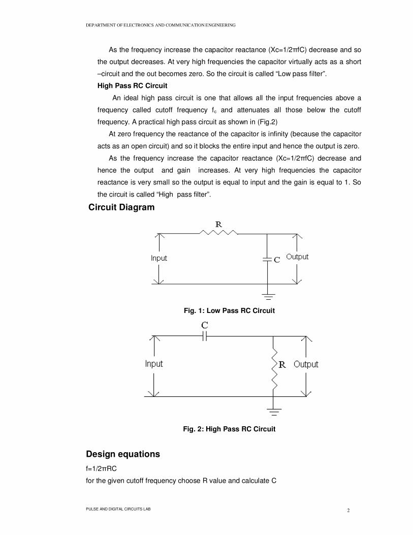
Circuit Diagram
Fig. 1: Low Pass RC Circuit
Fig. 2: High Pass RC Circuit
Design equations
f=1/2πRC
for the given cutoff frequency choose R value and calculate C
DEPARTMENT OF ELECTRONICS AND COMMUNICATION ENGINEERING
PULSE AND DIGITAL CIRCUITS LAB 3
Procedure
A) Frequency response characteristics
1. Connect the circuit as shown in Fig.1 and apply a sinusoidal signal of
amplitude of 2V p-p as input.
2. Vary the frequency of input signal in suitable steps of 100 Hz to 1 MHz and
measure the peak to peak amplitude of output signal.
3. Obtain frequency response characteristics of the circuit by calculating the gain
at each frequency and plotting gain in dB vs frequency in hertzs.
4. Find the cut off frequency fc by noting the value of f at 3 dB down from the
maximum gain
B) Output response
If the time constant of the circuit RC= 0.0198 ms
1. Apply a square wave of 2V p-p amplitude as input.
2. Adjust the time period of the waveform so that T>>RC, T=RC, T<<RC and
observe the output in each case.
3. Draw the input and output wave forms for different cases.
Readings
Table 1: Low Pass RC Circuit
Input Voltage, Vi=_____ V(p-p)
S.No Frequency
(Hz)
O/P Voltage, Vo
(V)
Gain = 20log(Vo/Vi)
(dB)
DEPARTMENT OF ELECTRONICS AND COMMUNICATION ENGINEERING
PULSE AND DIGITAL CIRCUITS LAB 4
Table 2: High Pass RC Circuit
Input Voltage, Vi=______ V(p-p)
S.No Frequency
(Hz)
O/P Voltage, Vo
(V)
Gain = 20log(Vo/Vi)
(dB)
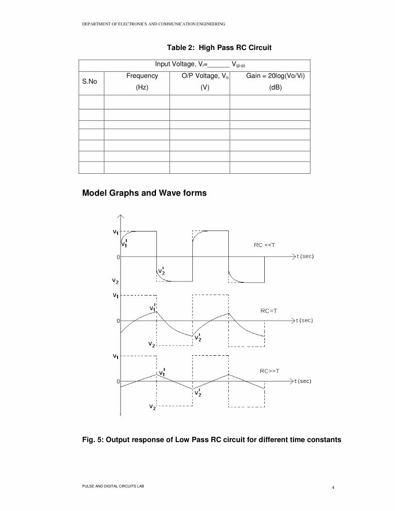
Model Graphs and Wave forms
Fig. 5: Output response of Low Pass RC circuit for different time constants

DEPARTMENT OF ELECTRONICS AND COMMUNICATION ENGINEERING
PULSE AND DIGITAL CIRCUITS LAB 5
Fig. 6: Output response of high Pass RC circuit for different time constants
Precautions
1. Connections should be made carefully.
2. Verify the circuit connections before giving supply.
3. Take readings without any parallax error.
Result
Inference
Questions
1. Define linear wave shaping?
2. When does the low pass circuit act as integrator?
3. When does the high pass circuit acts as a differentiator

DEPARTMENT OF ELECTRONICS AND COMMUNICATION ENGINEERING
PULSE AND DIGITAL CIRCUITS LAB 6
2. NON LINEAR WAVE SHAPPING-CLIPPERS
Aim
To verify the output response of different diode clamping circuits
Apparatus required
Name of the
Component/Equipment Specifications Quantity
Resistors 1KΩ 1
Diode 1N4007 1
CRO 20MHz 1
Function generator 1MHz 1
DC Regulated power
supply 0-30V,1A
1
Theory
The circuits for which the outputs are non-sinusoidal for sinusoidal inputs are
called “Nonlinear wave shaping circuits”. Examples for nonlinear wave shaping circuits
are clipper and clamping circuits.
Clippers
Clipping means cutting or removing a part. The basic action of a clipper circuit is
to remove certain portions of the waveform, above or below certain levels as per the
requirements. Thus the circuits which are used to clip off unwanted portion of the
waveform, without distorting the remaining part of the waveform are called “Clipper
circuits or Clippers”.
The half wave rectifier is the best and simplest type of clipper circuit which clips
off the positive/negative portion of the input signal. The clipper circuits are also called
voltage or current limiters, amplitude sectors or slicers.
The clippers are mainly classified into two types based on level of clipping.
1) Single level clippers: In this a single diode is used to perform single-ended
limiting at one independent level.
2) Two level clippers: In this a pair of diodes is used to perform double-ended
limiting at two independent levels. A parallel, a series, or a series-parallel
arrangement may be used.
DEPARTMENT OF ELECTRONICS AND COMMUNICATION ENGINEERING
PULSE AND DIGITAL CIRCUITS LAB 7
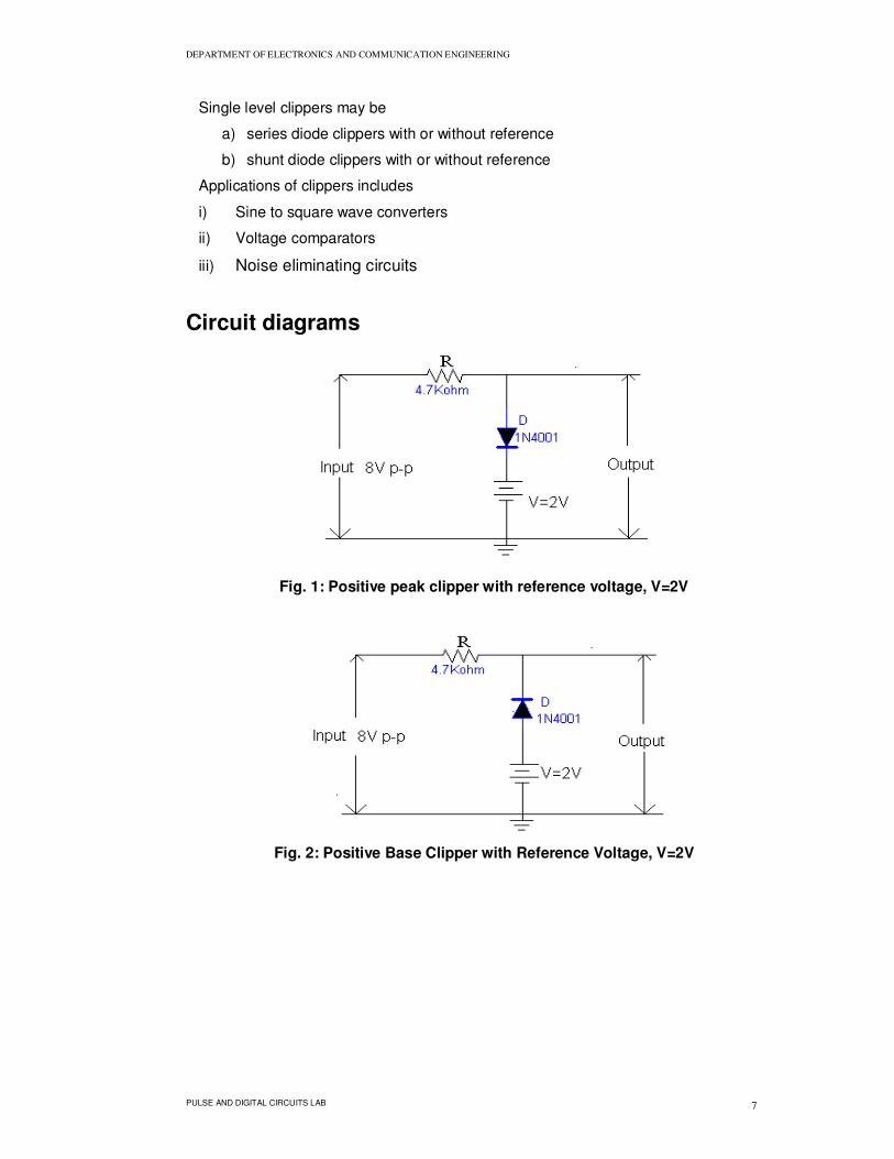
Single level clippers may be
a) series diode clippers with or without reference
b) shunt diode clippers with or without reference
Applications of clippers includes
i) Sine to square wave converters
ii) Voltage comparators
iii) Noise eliminating circuits
Circuit diagrams
Fig. 1: Positive peak clipper with reference voltage, V=2V
Fig. 2: Positive Base Clipper with Reference Voltage, V=2V
DEPARTMENT OF ELECTRONICS AND COMMUNICATION ENGINEERING
PULSE AND DIGITAL CIRCUITS LAB 8
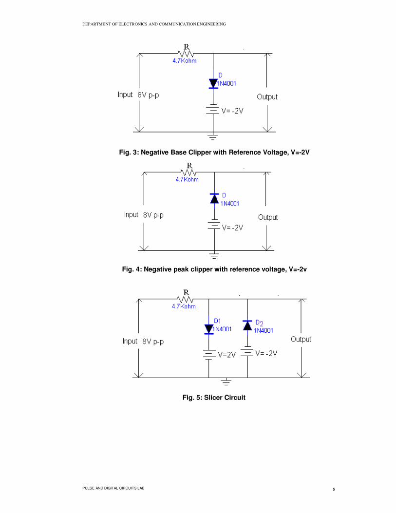
Fig. 3: Negative Base Clipper with Reference Voltage, V=-2V
Fig. 4: Negative peak clipper with reference voltage, V=-2v
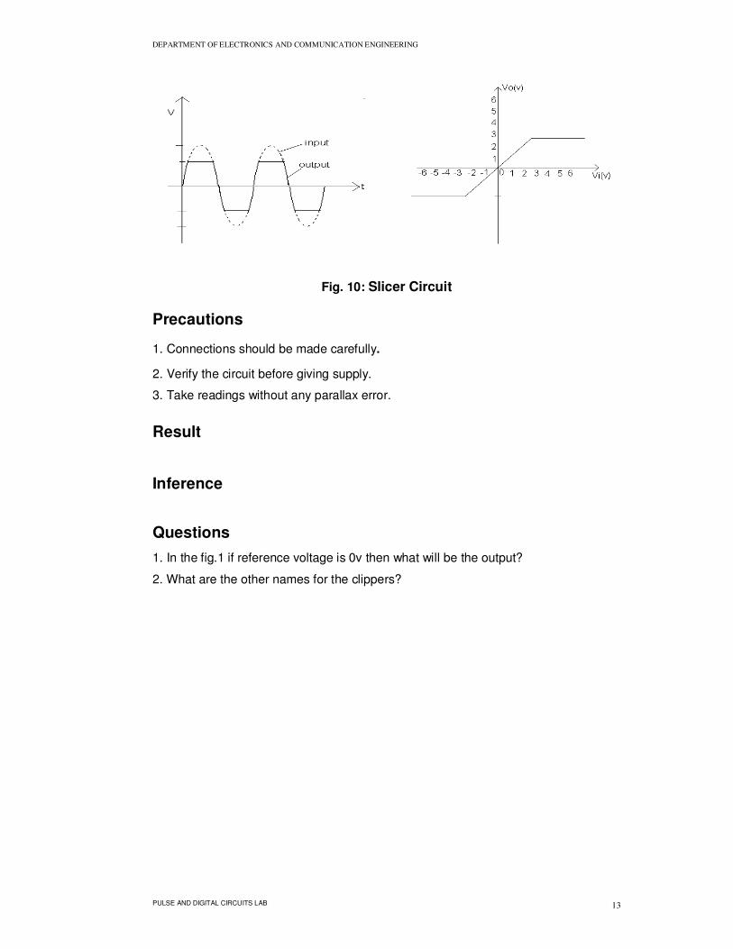
Fig. 5: Slicer Circuit
DEPARTMENT OF ELECTRONICS AND COMMUNICATION ENGINEERING
PULSE AND DIGITAL CIRCUITS LAB 9
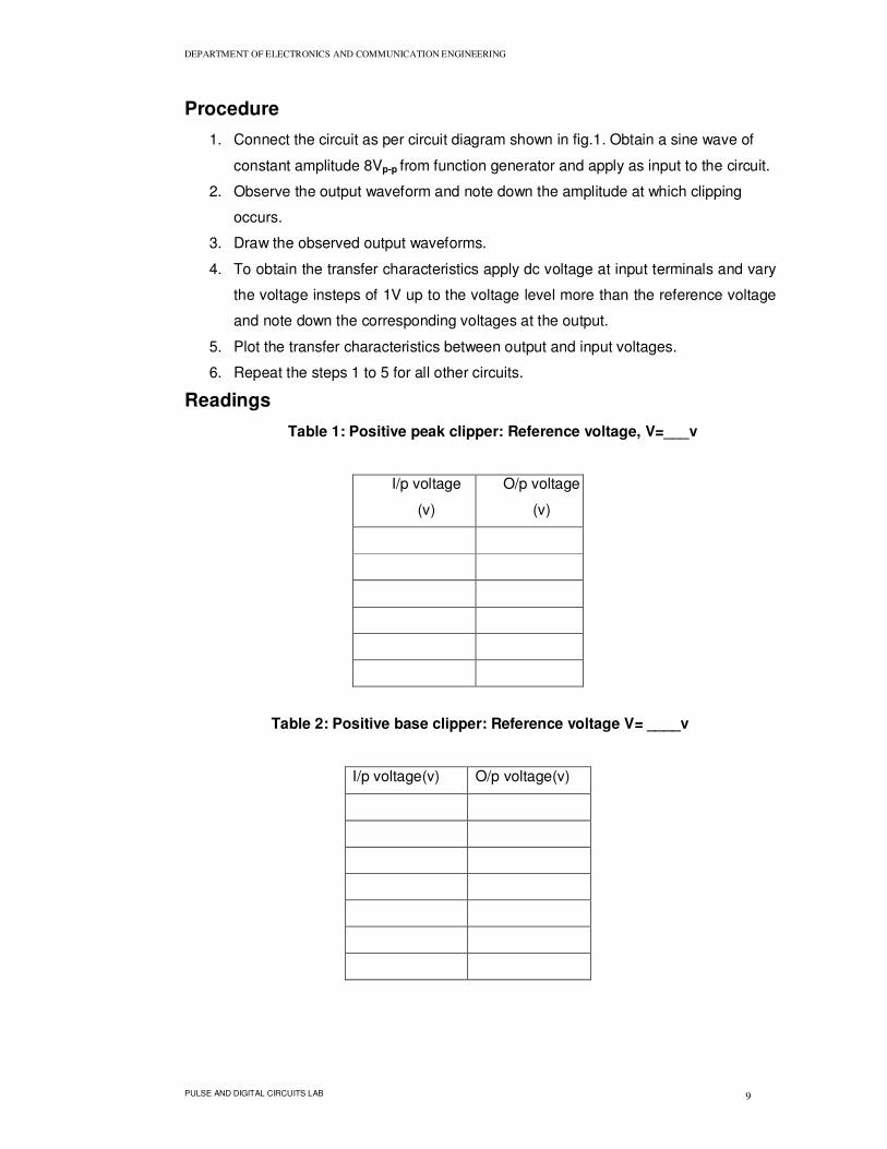
Procedure
1. Connect the circuit as per circuit diagram shown in fig.1. Obtain a sine wave of
constant amplitude 8Vp-p from function generator and apply as input to the circuit.
2. Observe the output waveform and note down the amplitude at which clipping
occurs.
3. Draw the observed output waveforms.
4. To obtain the transfer characteristics apply dc voltage at input terminals and vary
the voltage insteps of 1V up to the voltage level more than the reference voltage
and note down the corresponding voltages at the output.
5. Plot the transfer characteristics between output and input voltages.
6. Repeat the steps 1 to 5 for all other circuits.
Readings
Table 1: Positive peak clipper: Reference voltage, V=___v
I/p voltage
(v)
O/p voltage
(v)
Table 2: Positive base clipper: Reference voltage V= ____v
I/p voltage(v) O/p voltage(v)

DEPARTMENT OF ELECTRONICS AND COMMUNICATION ENGINEERING
PULSE AND DIGITAL CIRCUITS LAB 10
Table 3: Negative base clipper: Reference voltage V=___v
Table 4: Negative peak clipper: Reference voltage V= _____v
Table 5: Slicer Circuit
I/P voltage(v) O/Pvoltage(v)
I/P voltage(v) O/P voltage(v)
I/p voltage(v) O/p voltage(v)
DEPARTMENT OF ELECTRONICS AND COMMUNICATION ENGINEERING
PULSE AND DIGITAL CIRCUITS LAB 11
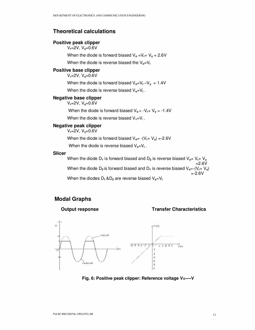
Theoretical calculations Positive peak clipper
Vr=2V, Vγ=0.6V
When the diode is forward biased Vo =Vr+ Vγ = 2.6V
When the diode is reverse biased the Vo=Vi
Positive base clipper Vr=2V, Vγ=0.6V
When the diode is forward biased Vo=Vr –Vγ = 1.4V
When the diode is reverse biased Vo=Vi .
Negative base clipper Vr=2V, Vγ=0.6V
When the diode is forward biased Vo = -Vr+ Vγ = -1.4V
When the diode is reverse biased Vo=Vi .
Negative peak clipper Vr=2V, Vγ=0.6V
When the diode is forward biased Vo= -(Vr+ Vγ) =-2.6V
When the diode is reverse biased Vo=Vi .
Slicer When the diode D1 is forward biased and D2 is reverse biased Vo= Vr+ Vγ
=2.6V When the diode D2 is forward biased and D1 is reverse biased Vo=-(Vr+ Vγ)
=-2.6V When the diodes D1 &D2 are reverse biased Vo=Vi
Modal Graphs
Output response Transfer Characteristics
Fig. 6: Positive peak clipper: Reference voltage V=----V
DEPARTMENT OF ELECTRONICS AND COMMUNICATION ENGINEERING
PULSE AND DIGITAL CIRCUITS LAB 12
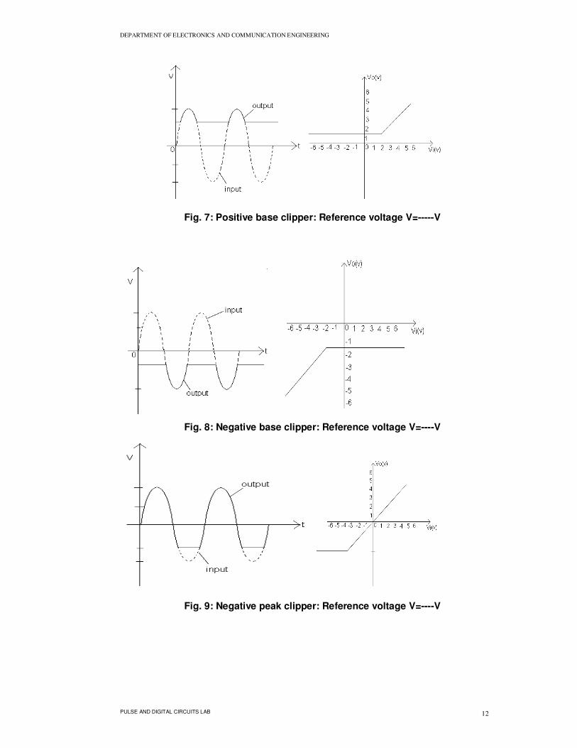
Fig. 7: Positive base clipper: Reference voltage V=-----V
Fig. 8: Negative base clipper: Reference voltage V=----V
Fig. 9: Negative peak clipper: Reference voltage V=----V
DEPARTMENT OF ELECTRONICS AND COMMUNICATION ENGINEERING
PULSE AND DIGITAL CIRCUITS LAB 13
Fig. 10: Slicer Circuit
Precautions
1. Connections should be made carefully.
2. Verify the circuit before giving supply.
3. Take readings without any parallax error.
Result
Inference
Questions
1. In the fig.1 if reference voltage is 0v then what will be the output?
2. What are the other names for the clippers?

DEPARTMENT OF ELECTRONICS AND COMMUNICATION ENGINEERING
PULSE AND DIGITAL CIRCUITS LAB 14
3. NON LINEAR WAVE SHAPPING-CLAMPERS
Aim
To verify the output response of different diode clamping circuits
Apparatus Required
Name of the
Component/Equipment
Specifications Quantity
Resistors 10KΩ 1
Capacitor 100uF, 100pF 1
Diode 1N4007 1
CRO 20MHz 1
Function generator 1MHz 1
Theory
Clampers
Clamping circuits are the circuits, which are used to clamp or fix the extremity of
a period wave form to some constant reference level Vr .These are also use.d to add a
d.c level as per the requirement to the a.c signals. Capacitor, diode, resistor are the
three basic elements of a clamper circuit.
The Clamping Circuit Theorem
When a signal is transmitted through a capacitive coupling network (RC high –
pass circuit), it looses its dc component, and a clamping circuit may be used to introduce
a dc component by fixing the positive or negative extremity of that waveform to some
reference level. For this reason, the clamping circuit is often referred to as dc restorer
or dc reinserter.
Classification: Basically clampers are classified in to
1. Negative clampers: In negative clamping, the positive extremity of the
waveform is fixed at the reference level and the entire waveform appears below the
reference level, i.e. the output waveform is negatively clamped with reference to the
reference level.
2. Positive clampers: In positive clamping, the negative extremity of the
waveform is fixed at the reference level and the entire waveform appears above the
reference level, i.e. the output waveform is positively clamped with reference to the
reference level.

DEPARTMENT OF ELECTRONICS AND COMMUNICATION ENGINEERING
PULSE AND DIGITAL CIRCUITS LAB 15
The capacitor is essential in clamping circuits. The difference between the
clipping and clamping circuits is that while the clipper clips off an unwanted portion of the
input waveform, the clamper simply clamps the maximum positive or negative peak of
the waveform to a desire level. There will be no distortion of waveform.
Circuit Diagrams
Fig. 11: Positive peak clamping to 0V
Fig. 12: Positive peak clamping to Vr=----
Fig. 13: Negative peak clamping to Vr=0v
DEPARTMENT OF ELECTRONICS AND COMMUNICATION ENGINEERING
PULSE AND DIGITAL CIRCUITS LAB 16
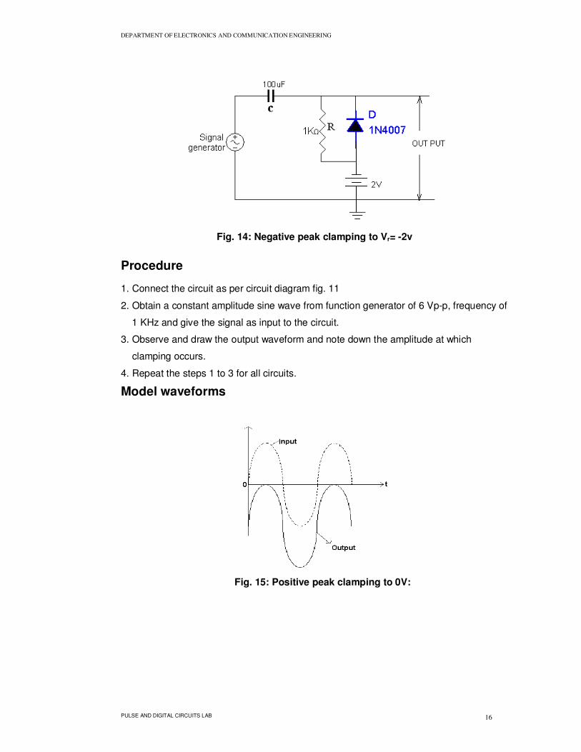
Fig. 14: Negative peak clamping to Vr= -2v
Procedure
1. Connect the circuit as per circuit diagram fig. 11
2. Obtain a constant amplitude sine wave from function generator of 6 Vp-p, frequency of
1 KHz and give the signal as input to the circuit.
3. Observe and draw the output waveform and note down the amplitude at which
clamping occurs.
4. Repeat the steps 1 to 3 for all circuits.
Model waveforms
Fig. 15: Positive peak clamping to 0V:
DEPARTMENT OF ELECTRONICS AND COMMUNICATION ENGINEERING
PULSE AND DIGITAL CIRCUITS LAB 17
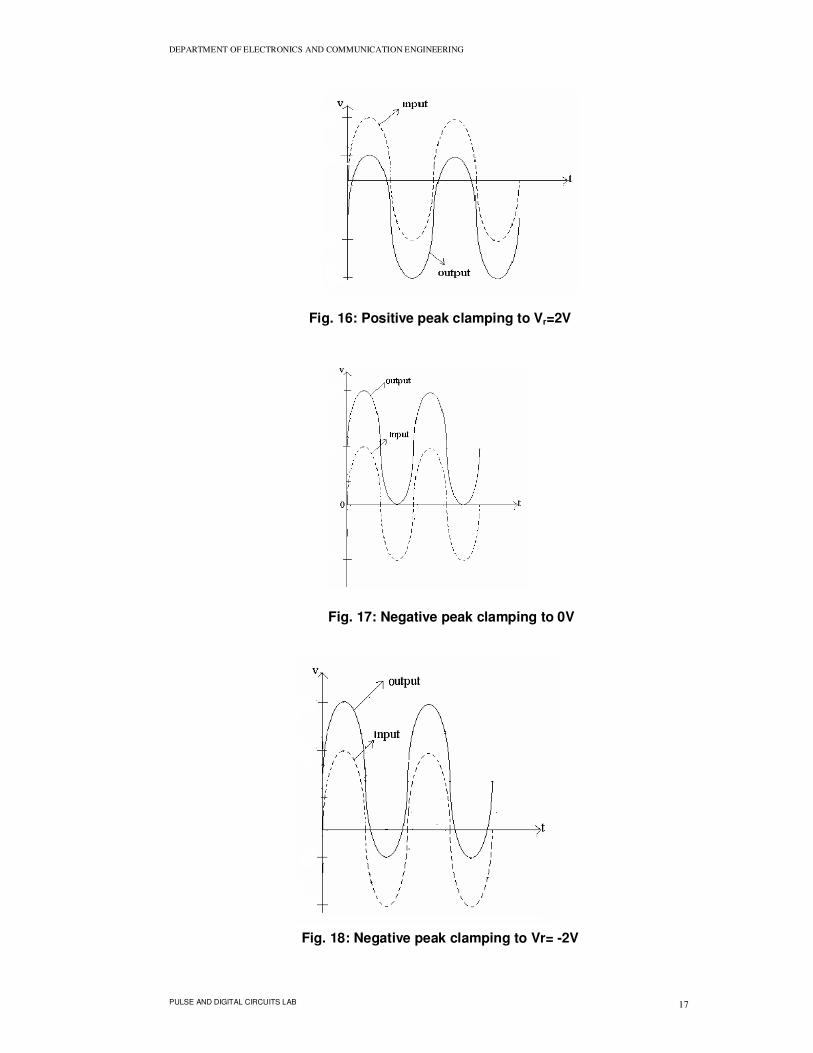
Fig. 16: Positive peak clamping to Vr=2V
Fig. 17: Negative peak clamping to 0V
Fig. 18: Negative peak clamping to Vr= -2V

DEPARTMENT OF ELECTRONICS AND COMMUNICATION ENGINEERING
PULSE AND DIGITAL CIRCUITS LAB 18
Precautions
1. Connections should be made carefully.
2. Verify the circuit before giving supply.
3. Take readings without any parallax error.
Result
Inference
Questions
1. What is a clamper?
2. Give some practical applications of clamper.
3. What is the purpose of shunt resistance in clamper?

DEPARTMENT OF ELECTRONICS AND COMMUNICATION ENGINEERING
PULSE AND DIGITAL CIRCUITS LAB 19
4. TRANSISTOR AS A SWITCH
Aim
To verifying the switching action of a transistor.
Apparatus Required
Name of the
Component/Equipment Specifications Quantity
Transistor BC 107 1
Resistors 10K 2
5.6KΩ 2
Capacitor 100pF 1
CRO 20MHz 1
Function generator 1MHz 1
Regulated Power Supply 0-30V, 1A 1
Theory
Transistors are widely used in digital logic circuits and switching applications. In
these applications the voltage levels periodically alternate between a “LOW” and a
“HIGH” voltage, such as 0V and +5V.
In switching circuits, a transistor is operated at cutoff for the OFF condition, and
in saturation for the ON condition. The active linear region is passed through abruptly
switching from cutoff to saturation or vice-versa. In switching applications, the active
region is of no interest.
In cutoff region, both the transistor junctions between Emitter and Base and the
junction between Base and Collector are reverse biased and only the reverse current
which is very small and practically neglected, flows in the transistor.
In saturation region both junctions are in forward bias and the values of Vce(sat)
and Vbe(sat) are small. Saturation voltages range from a few tenths of a volt to a volt,
depending on the transistor type. In saturation condition, the collector current is
comparatively large, and is controlled by the external resistance connected in the
collector circuit. The basic transistor circuit used in switching operations is called an
“Inverter”.
DEPARTMENT OF ELECTRONICS AND COMMUNICATION ENGINEERING
PULSE AND DIGITAL CIRCUITS LAB 20
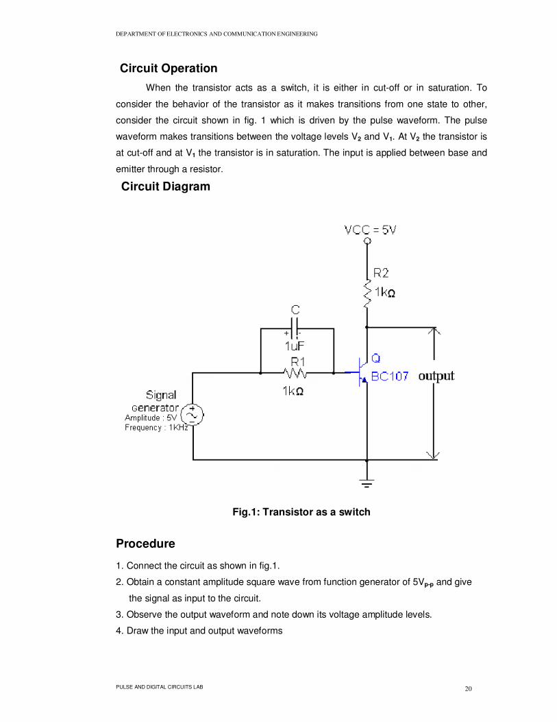
Circuit Operation
When the transistor acts as a switch, it is either in cut-off or in saturation. To
consider the behavior of the transistor as it makes transitions from one state to other,
consider the circuit shown in fig. 1 which is driven by the pulse waveform. The pulse
waveform makes transitions between the voltage levels V2 and V1. At V2 the transistor is
at cut-off and at V1 the transistor is in saturation. The input is applied between base and
emitter through a resistor.
Circuit Diagram
Fig.1: Transistor as a switch
Procedure
1. Connect the circuit as shown in fig.1.
2. Obtain a constant amplitude square wave from function generator of 5Vp-p and give
the signal as input to the circuit.
3. Observe the output waveform and note down its voltage amplitude levels.
4. Draw the input and output waveforms
DEPARTMENT OF ELECTRONICS AND COMMUNICATION ENGINEERING
PULSE AND DIGITAL CIRCUITS LAB 21
Model graph
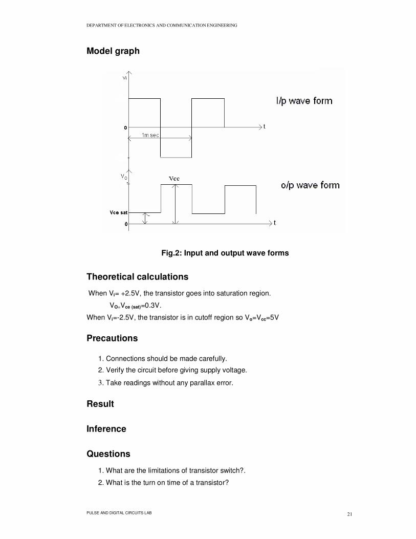
Fig.2: Input and output wave forms
Theoretical calculations
When Vi= +2.5V, the transistor goes into saturation region.
VO=Vce (sat)=0.3V.
When Vi=-2.5V, the transistor is in cutoff region so Vo=Vcc=5V
Precautions
1. Connections should be made carefully.
2. Verify the circuit before giving supply voltage.
3. Take readings without any parallax error.
Result
Inference
Questions
1. What are the limitations of transistor switch?.
2. What is the turn on time of a transistor?
DEPARTMENT OF ELECTRONICS AND COMMUNICATION ENGINEERING
PULSE AND DIGITAL CIRCUITS LAB 22
5. STUDY OF LOGIC GATES
AAiimm
To construct the basic and universal gates using discrete components and vverify
their truth tables
Apparatus required
Name of the
Component/Equipment Specifications Quantity
Transistor BC 107 1
Diode IN4007 1
Resistors 4.7KΩ 2
100KΩ 1
LED - 1
Bread Board - 1
Regulated Power Supply 0-30V, 1A 1
TThheeoorryy
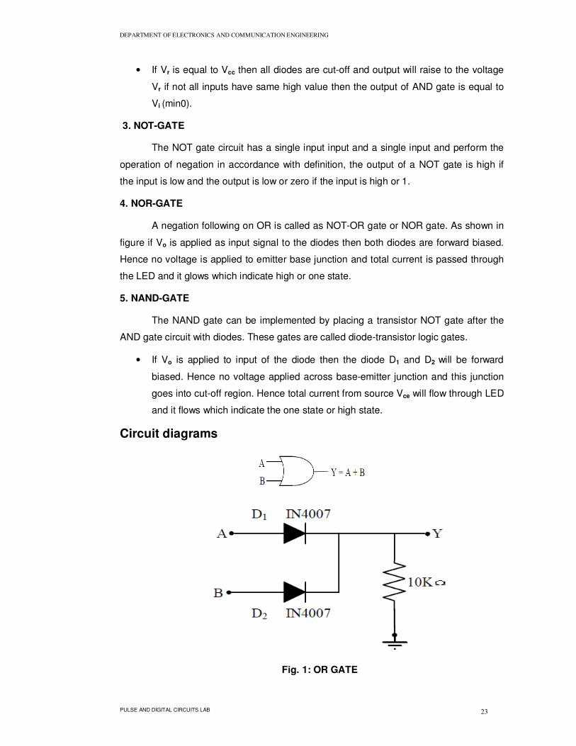
1. OR-GATE
OR gate has two or more inputs and a single output and it operates in
accordance with the following definitions.
• The output of an OR gate is high if one or more inputs are high. When all the
inputs are low then the output is low.
• If two or more inputs are in high state then the diodes connected to these inputs
conduct and all other diodes remain reverse biased so the output will be high and
OR function is satisfied.
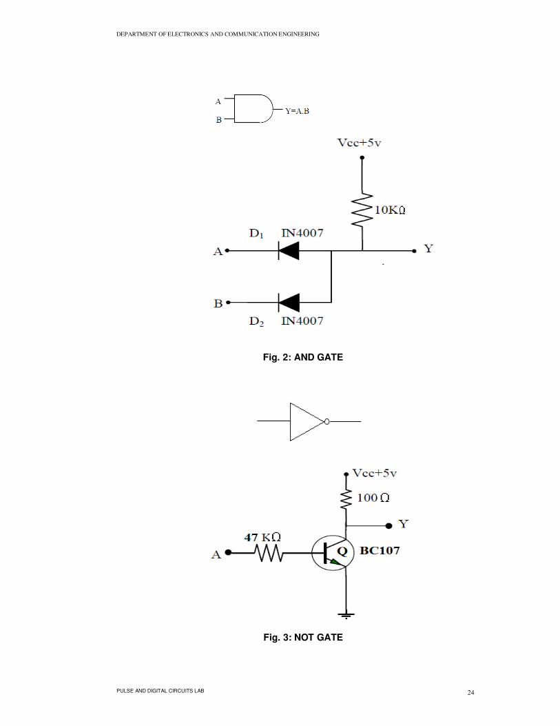
2. AND-GATE
AND gate has two or more inputs and a single output and it operates in
accordance with the following definitions.
• The output of an AND gate is high if all inputs are high.
• If Vin is chosen i.e. more positive than Vcc then all diodes will be conducting upon
a coincidence and the output will be clamped to ‘1’.
DEPARTMENT OF ELECTRONICS AND COMMUNICATION ENGINEERING
PULSE AND DIGITAL CIRCUITS LAB 23
• If Vr is equal to Vcc then all diodes are cut-off and output will raise to the voltage
Vr if not all inputs have same high value then the output of AND gate is equal to
Vi (min0).
3. NOT-GATE
The NOT gate circuit has a single input input and a single input and perform the
operation of negation in accordance with definition, the output of a NOT gate is high if
the input is low and the output is low or zero if the input is high or 1.
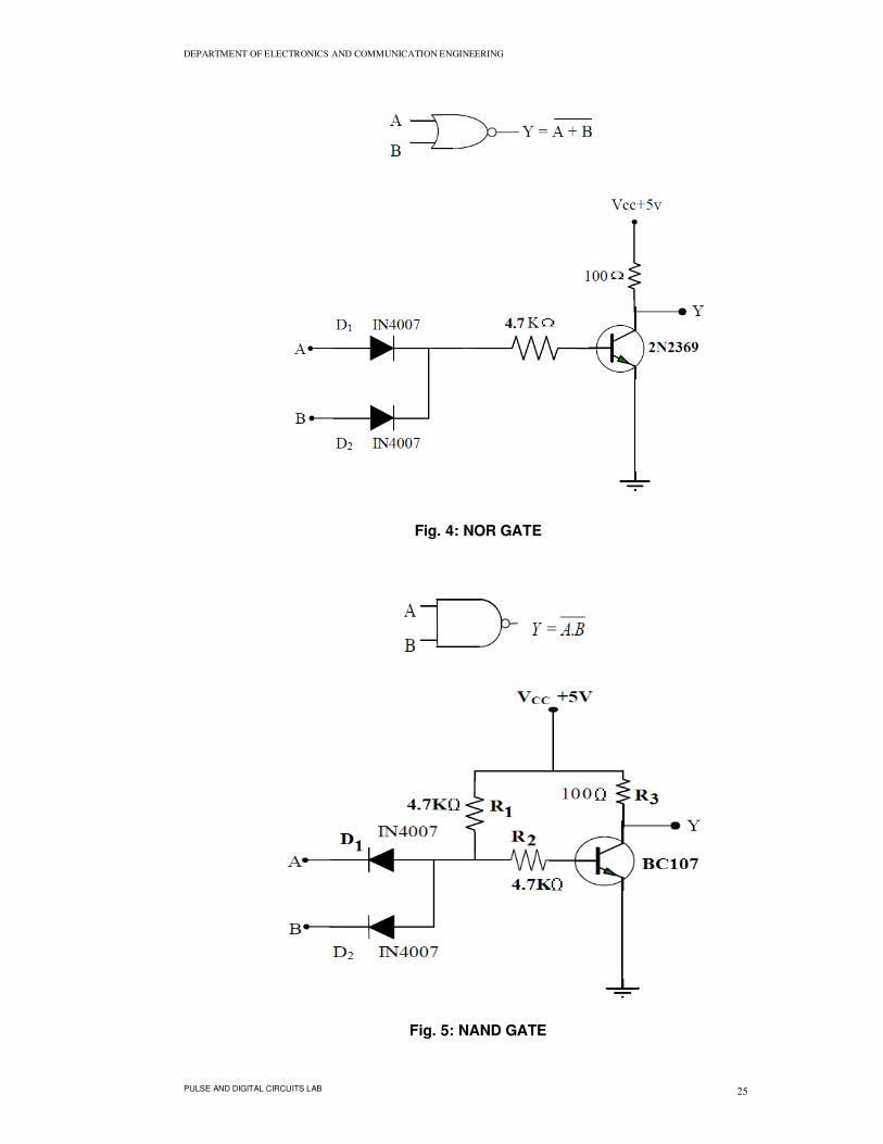
4. NOR-GATE
A negation following on OR is called as NOT-OR gate or NOR gate. As shown in
figure if Vo is applied as input signal to the diodes then both diodes are forward biased.
Hence no voltage is applied to emitter base junction and total current is passed through
the LED and it glows which indicate high or one state.
5. NAND-GATE
The NAND gate can be implemented by placing a transistor NOT gate after the
AND gate circuit with diodes. These gates are called diode-transistor logic gates.
• If Vo is applied to input of the diode then the diode D1 and D2 will be forward
biased. Hence no voltage applied across base-emitter junction and this junction
goes into cut-off region. Hence total current from source Vce will flow through LED
and it flows which indicate the one state or high state.
Circuit diagrams
Fig. 1: OR GATE
DEPARTMENT OF ELECTRONICS AND COMMUNICATION ENGINEERING
PULSE AND DIGITAL CIRCUITS LAB 24
Fig. 2: AND GATE
Fig. 3: NOT GATE
DEPARTMENT OF ELECTRONICS AND COMMUNICATION ENGINEERING
PULSE AND DIGITAL CIRCUITS LAB 25
Fig. 4: NOR GATE
Fig. 5: NAND GATE
DEPARTMENT OF ELECTRONICS AND COMMUNICATION ENGINEERING
PULSE AND DIGITAL CIRCUITS LAB 26
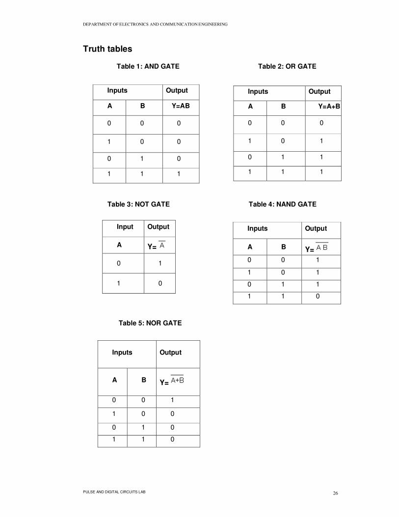
Truth tables
Table 1: AND GATE Table 2: OR GATE
Table 3: NOT GATE Table 4: NAND GATE
Table 5: NOR GATE
Inputs Output
A B Y=AB
0 0 0
1 0 0
0 1 0
1 1 1
Inputs Output
A B Y=A+B
0 0 0
1 0 1
0 1 1
1 1 1
Input Output
A Y=
0 1
1 0
Inputs Output
A B Y=
0 0 1
1 0 1
0 1 1
1 1 0
Inputs Output
A B Y=
0 0 1
1 0 0
0 1 0
1 1 0
DEPARTMENT OF ELECTRONICS AND COMMUNICATION ENGINEERING
PULSE AND DIGITAL CIRCUITS LAB 27
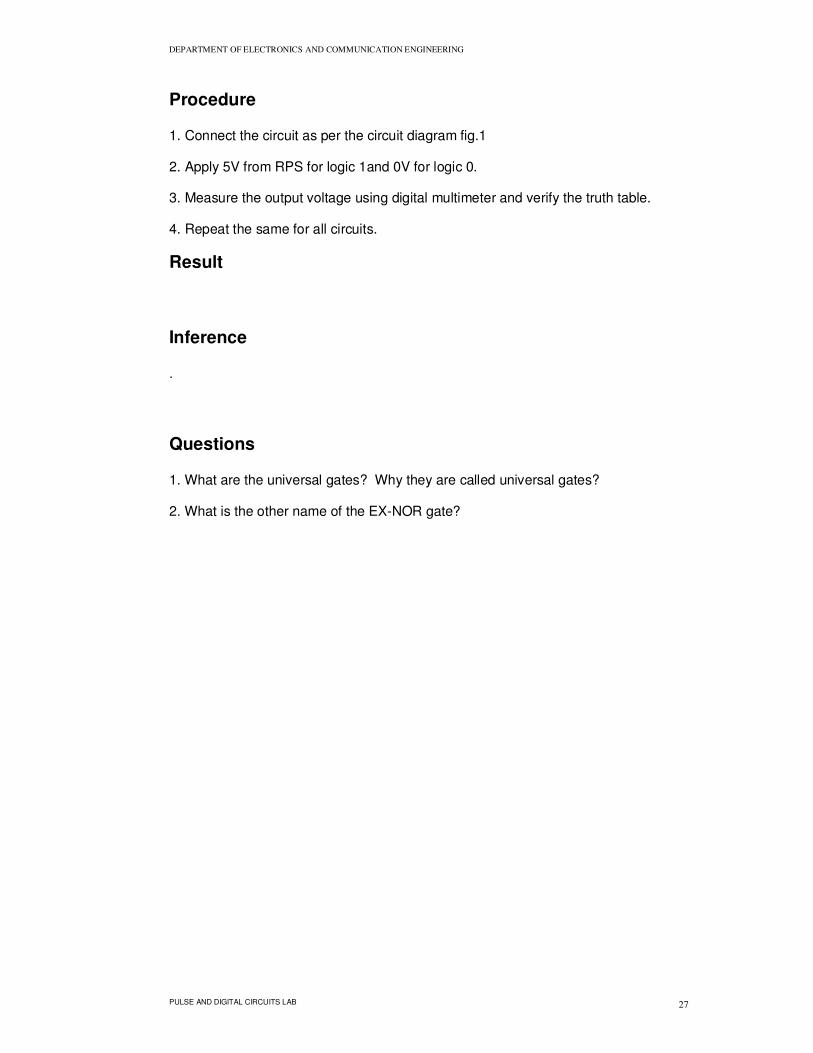
Procedure
1. Connect the circuit as per the circuit diagram fig.1
2. Apply 5V from RPS for logic 1and 0V for logic 0.
3. Measure the output voltage using digital multimeter and verify the truth table.
4. Repeat the same for all circuits.
Result
Inference
.
Questions
1. What are the universal gates? Why they are called universal gates?
2. What is the other name of the EX-NOR gate?
DEPARTMENT OF ELECTRONICS AND COMMUNICATION ENGINEERING
PULSE AND DIGITAL CIRCUITS LAB 28
6. STUDY OF FLIP FLOPS
Aim
To verify truth tables of D and T flip-flops.
Apparatus required:
Name of the
Component/Equipment
Specifications Quantity
IC 7476 - 1
IC 7404 - 1
Digital Trainer - 1
Theory
Flip-flop is a digital circuit which is having a combinational circuit and a memory
unit .so the output of flip flop is depends upon the previous state of the outputs. This flip-
flop consists two outputs one is complemented of the other. These flip-flops are having
very many applications in digital circuitry.
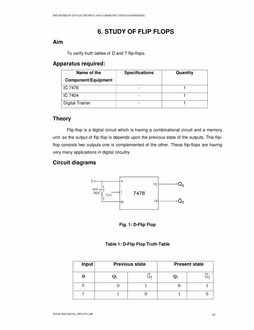
Circuit diagrams
Fig. 1: D-Flip Flop
Table 1: D-Flip Flop Truth Table
Input Previous state Present state
D Q1 Q1
0 0 1 0 1
1 1 0 1 0
DEPARTMENT OF ELECTRONICS AND COMMUNICATION ENGINEERING
PULSE AND DIGITAL CIRCUITS LAB 29
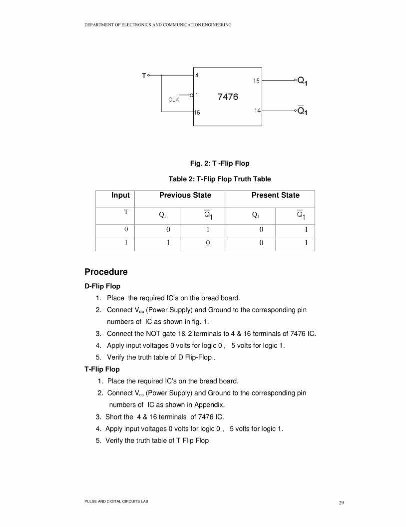
Fig. 2: T -Flip Flop
Table 2: T-Flip Flop Truth Table
Input Previous State Present State
T Q1
Q1
0 0 1 0 1
1 1 0 0 1
Procedure
D-Flip Flop
1. Place the required IC’s on the bread board.
2. Connect Vcc (Power Supply) and Ground to the corresponding pin
numbers of IC as shown in fig. 1.
3. Connect the NOT gate 1& 2 terminals to 4 & 16 terminals of 7476 IC.
4. Apply input voltages 0 volts for logic 0 , 5 volts for logic 1.
5. Verify the truth table of D Flip-Flop .
T-Flip Flop
1. Place the required IC’s on the bread board.
2. Connect Vcc (Power Supply) and Ground to the corresponding pin
numbers of IC as shown in Appendix.
3. Short the 4 & 16 terminals of 7476 IC.
4. Apply input voltages 0 volts for logic 0 , 5 volts for logic 1.
5. Verify the truth table of T Flip Flop
DEPARTMENT OF ELECTRONICS AND COMMUNICATION ENGINEERING
PULSE AND DIGITAL CIRCUITS LAB 30
Result
Inference
Questions
1. What is the drawback of the JK-Flip Flop?
2. What are the applications of D and T flip Flops?
DEPARTMENT OF ELECTRONICS AND COMMUNICATION ENGINEERING
PULSE AND DIGITAL CIRCUITS LAB 31
7. ASTABLE MULTIVIBRATOR
Aim
To observe the ON & OFF states an Astable Multivibrator.
Apparatus required
Name of the
Component/Equipment Specifications Quantity
Transistor BC 107 2
Resistors 3.9KΩ 2
100KΩ 2
Capacitor 0.01µF 2
Regulated Power Supply 0-30V, 1A 1
Theory
Multivibrator
Multi means many ; vibrator means oscillator. A circuit which can oscillate at a
number of frequencies is called a Multivibrator. Each multivibrator has two states.
Astable Multivibrator
An astable multivibrator has no stable state. And it is having two quasi stable
states. In astable multivibrator circuit both the coupling elements are capacitors (i.e. ac
couplings). And it keeps on switching between these two states by itself. No external
triggering signal is needed. The astable multivibrator cannot remain indefinitely in any
one of the two states .The two amplifier stages of an astable multivibrator are
regenerative across coupled by capacitors. The astable multivibrator may be to
generate a square wave of period,1.38RC. The astable multivibrator circuit is used as a
master oscillator to generate square waves. It is often a basic source of fast waveforms.
It is a free running oscillator. It is called a “Square wave generator”. It is also termed a
“Relaxation oscillator”.
Circuit Operation
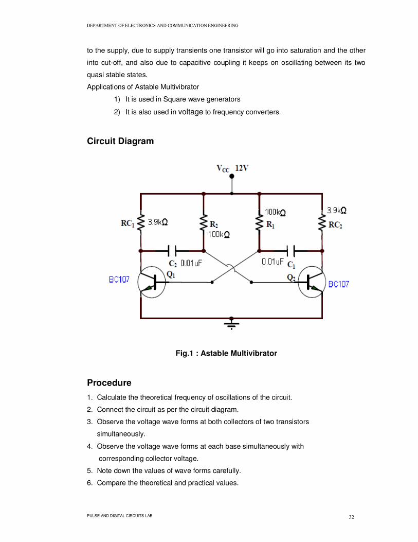
The circuit diagram of the collector – coupled astable multivibrator using
transistors as shown in fig.1. The collectors of both the transistors Q1 & Q2 are connected
to the bases of the other transistors through the coupling capacitors C1 & C2. Since both
are ac couplings, neither transistor can remain permanently at cut-off. Instead, the circuit
has two quasi-stable states, and it makes periodic transistors between these states.
Hence it is used as a master oscillator. No triggering signal is required for this
multivibrator. The component values are selected such that, the moment it is connected
DEPARTMENT OF ELECTRONICS AND COMMUNICATION ENGINEERING
PULSE AND DIGITAL CIRCUITS LAB 32
to the supply, due to supply transients one transistor will go into saturation and the other
into cut-off, and also due to capacitive coupling it keeps on oscillating between its two
quasi stable states.
Applications of Astable Multivibrator
1) It is used in Square wave generators
2) It is also used in voltage to frequency converters.
Circuit Diagram
Fig.1 : Astable Multivibrator
Procedure
1. Calculate the theoretical frequency of oscillations of the circuit.
2. Connect the circuit as per the circuit diagram.
3. Observe the voltage wave forms at both collectors of two transistors
simultaneously.
4. Observe the voltage wave forms at each base simultaneously with
corresponding collector voltage.
5. Note down the values of wave forms carefully.
6. Compare the theoretical and practical values.
DEPARTMENT OF ELECTRONICS AND COMMUNICATION ENGINEERING
PULSE AND DIGITAL CIRCUITS LAB 33
Calculations
Theoretical Values
RC= R1C1+ R2C2
Time Period, T = 1.368RC
= 1.368x100x103x0.01x10-6
= 93 µ sec
= 0.093 m sec
Frequency, f = 1/T = 10.75kHz.
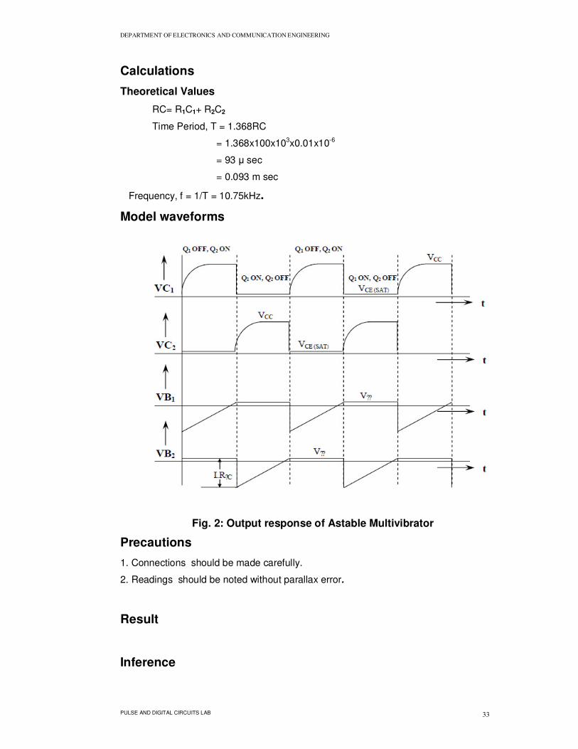
Model waveforms
Fig. 2: Output response of Astable Multivibrator
Precautions
1. Connections should be made carefully.
2. Readings should be noted without parallax error.
Result
Inference

DEPARTMENT OF ELECTRONICS AND COMMUNICATION ENGINEERING
PULSE AND DIGITAL CIRCUITS LAB 34
Questions
1.Define stable state ?
2.Define quasi stable state ?
DEPARTMENT OF ELECTRONICS AND COMMUNICATION ENGINEERING
PULSE AND DIGITAL CIRCUITS LAB 35
8. BISTABLE MULTIVIBRATOR
Aim
To observe the stable state voltages of Bitable Multivibrator.
Apparatus required
Name of the
Component/Equipment Specifications Quantity
Transistor BC 107 2
Resistors 2.2KΩ 2
12KΩ 2
Regulated Power Supply 0-30V, 1A 1
Digital multi meter 3 ½ digit display 1
Theory
Multivibrator
Multi means many ; vibrator means oscillator. A circuit which can oscillate at a
number of frequencies is called a Multivibrator. Each multivibrator has two states.
Bistable Multivibrator
A bistable multivibrator has two stable states. Each multivibrator is having
two coupling elements. In bistable multivibrator circuit both the coupling elements are
resistors (i.e. dc couplings). It requires a triggering signal to change from one stable state
to another, and another triggering signal for the reverse transition.
A bistable multivibrator is also called as a multi, Eccles-Jordan circuit, trigger
circuit, scale –of-two toggle circuit, flip-flop, and binary.
Circuit Operation
The circuit diagram of a fixed bias bistable multivibrator using transistors is as
shown in fig. 1. The output of each amplifier is direct coupled to the input of the other
amplifier. In one of the stable states transistor Q1 and Q2 is off and in the other stable
state. Q1 is off and Q2 is on even though the circuit is symmetrical; it is not possible for
the circuit to remain in a stable state with both the transistors conducting simultaneously
and caring equal currents. The reason is that if we assume that both the transistors are
biased equally and are carrying equal currents i1 and i2 suppose there is a minute
fluctuation in the current i1-let us say it increases by a small amount .Then the voltage at
the collector of Q1 decreases. This will result in a decrease in voltage at the base of Q2.

DEPARTMENT OF ELECTRONICS AND COMMUNICATION ENGINEERING
PULSE AND DIGITAL CIRCUITS LAB 36
So Q2 conducts less and i2 decreases and hence the potential at the collector of q2
increases. This results in an increase in the base potential of Q1. So Q1 conducts still
more and i1 is further increased and the potential at the collector of Q1 is further
decreased, and so on. So the current i1 keeps on increasing and the current i2 keeps on
decreasing till Q1 goes in to saturation and Q2 goes in to cut-off. This action takes place
because of the regenerative feed –back incorporated into the circuit and will occur only if
the loop gain is greater than one.
Applications of Bistable Multivibrator
1) It is used as a basic memory element
2) It is used to perform many digital operations such as counting, storing of binary
data.
3) It is also used in the generation & processing of pulse type waveform.
Circuit Diagram
Fig.1: Bistable Multivibrator
Procedure
1. Connect the circuit as shown in fig.1
2. Verify the stable state by measuring the voltages at two collectors by using
multimeter.
3. Note down the corresponding base voltages of the same state (say state-1).
4. To change the state, apply negative voltage (say-2v) to the base of on
Transistor or positive voltage to the base of transistor (through proper
current limiting resistance).
5. Verify the state by measuring voltages at collector and also note down
voltages at each base.
DEPARTMENT OF ELECTRONICS AND COMMUNICATION ENGINEERING
PULSE AND DIGITAL CIRCUITS LAB 37
Observations
Before Triggering
Q1 Q2
VBE1= VBE2=
VCE1= VCE2=
After Triggering
Q1 Q2
VBE1= VBE2=
VCE1= VCE2=
Precautions
1. Connections should be made carefully.
2. Note down the parameters carefully.
3. The supply voltage levels should not exceed the maximum rating of the transistor.
Inference
Result
Questions
1. What do you mean by a bistable circuit?
2. What are the other names of a bistable multivibrator?
3. What do you mean by triggering signal?

DEPARTMENT OF ELECTRONICS AND COMMUNICATION ENGINEERING
PULSE AND DIGITAL CIRCUITS LAB 38
9. MONOSTABLE MULTIVIBRATOR
Aim
To observe the stable state and quasi stable state voltages of monostable
multivibrator.
Apparatus Required
Name of the
Component/Equipment Specifications Quantity
Transistor BC 107 2
Resistors
1.5KΩ 1
2.2KΩ 2
68KΩ 1
1KΩ 1
Capacitor 1µF 2
Diode 0A79 1
CRO 20MHz 1
Function generator 1MHz 1
Regulated Power Supply (0-30V), 1A 1
Theory
Multi means many ; vibrator means oscillator. A circuit which can oscillate at a
number of frequencies is called a Multivibrator. Each multivibrator has two states.
Monostable Multivibrator
A monostable multivibrator on the other hand compared to astable, bistable has
only one stable state, the other state being quasi stable state. Normally the monostable
multivibrator is in stable state and when an externally triggering pulse is applied, it
switches from the stable to the quasi stable state. It remains in the quasi stable state for
a short duration, but automatically reverse switches back to its original stable state
without any triggering pulse.
The monostable multivibrator is also called as ‘one shot’ or ‘uni vibrator’ since
only one triggering signal is required to reverse the original stable state. The duration of
quasi stable state is termed as delay time (or) pulse width (or) gate time. It is denoted
as ‘t’
DEPARTMENT OF ELECTRONICS AND COMMUNICATION ENGINEERING
PULSE AND DIGITAL CIRCUITS LAB 39
Circuit Operation
Under quiescent conditions, the monostable multivibrator will be in its stable state
only. A triggering signal is required to induce a transition from the stable state to the
quasi stable state. Once triggered properly the circuit may remain in its quasi stable state
for a time which is very long compared with the time of transition between the states, and
after that it will return to its original state. No external triggering signal is required to
induce this reverse operation. In monostable multivibrator one coupling element is a
resistor & another coupling element is capacitor.
When triggered, since the circuit returns to its original state by itself after a time T,
it is known as a one shot, single-step, or a univibrator. Since it generates a rectangular
waveform which can be used to gate other circuits, it is also called a gating circuit.
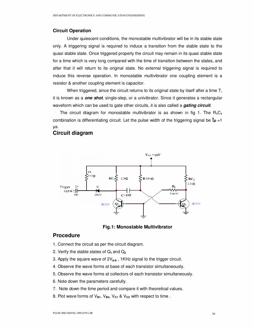
The circuit diagram for monostable multivibrator is as shown in fig 1. The R1C1
combination is differentiating circuit. Let the pulse width of the triggering signal be tp =1
µs.
Circuit diagram
Fig.1: Monostable Multivibrator
Procedure
1. Connect the circuit as per the circuit diagram.
2. Verify the stable states of Q1 and Q2
3. Apply the square wave of 2Vp-p , 1KHz signal to the trigger circuit.
4. Observe the wave forms at base of each transistor simultaneously.
5. Observe the wave forms at collectors of each transistor simultaneously.
6. Note down the parameters carefully.
7. Note down the time period and compare it with theoretical values.
8. Plot wave forms of VB1, VB2, VC1 & VC2 with respect to time .

DEPARTMENT OF ELECTRONICS AND COMMUNICATION ENGINEERING
PULSE AND DIGITAL CIRCUITS LAB 40
Model waveforms
Fig. 2: Output response of Monostable Multivibrator
Calculations
Theoretical Values
Time Period, T = 0.693RC
= 0.693x68x103x0.01x10-6
= 47µ sec
= 0.047 m sec
Frequency, f = 1/T = 21 kHz
Precautions
1. Connections should be made carefully.
2. Note down the parameters without parallax error.
3. The supply voltage levels should not exceed the maximum rating of the transistor.

DEPARTMENT OF ELECTRONICS AND COMMUNICATION ENGINEERING
PULSE AND DIGITAL CIRCUITS LAB 41
Inference
Result
.
Questions
1. What are the other names of Mono Stable multivibrator ?
2. Which type of triggering is used in mono stable multi vibrator ?
3. Define transition time?

DEPARTMENT OF ELECTRONICS AND COMMUNICATION ENGINEERING
PULSE AND DIGITAL CIRCUITS LAB 42
10. SAMPLING GATES
Aim
To observe the output response of a bidirectional sampling gate.
Apparatus Required
Name of the
Component/Equipment Specifications Quantity
Transistor BC 107 1
Resistors 220KΩ 1
5.6KΩ 1
CRO 20MHz 1
Function generator 1MHz 2
Regulated Power Supply (0-30V), 1A 1
Theory
Sampling gate is a transmission network in which the output is an exact
reproduction of the input during a selected time interval and is zero otherwise. The time
interval for transmission is selected by an externally impressed signal which is called the
gating signal and is usually rectangular in wave shape.
Sampling gates are of two types
1. Unidirectional sampling gates: Unidirectional sampling gates are those which
transmit signals of only one polarity.
2. Bidirectional sampling gates: Bidirectional sampling gates are those which transmit
signals of both polarities.
When gating signal is at it’s lower level transistor is well cutoff and output is Vcc.
When gating signal is at its higher level transistor goes into active region so input signal
is sampled and appears at output.
Sampling gates are also called linear gates, transmission gates or selection circuits.
Sampling gates are different from the logic gates. In logic gates there can be any
number of inputs and the inputs and output of the logic gates are either pulses or voltage
levels and the output is not a reproduction of the input. The output of a sampling gate is
an exact reproduction of the input during the selected time interval. The input may be a
pulse, square wave, sine wave or any other waveform.

DEPARTMENT OF ELECTRONICS AND COMMUNICATION ENGINEERING
PULSE AND DIGITAL CIRCUITS LAB 43
Circuit diagram
Fig. 1: Bidirectional Sampling gate using transistor
Procedure
1. Connect the circuit as per shown in fig.1.
2. Generate a control voltage Vc of 4V peak to peak voltage 1KHz and apply it to the
circuit.
3. Apply the input signal with a small peak to peak voltage.
4. Observe the output wave form and control voltage, VC simultaneously and note
down the parameters of waveforms.
5. Plot the graph between VS, VC and output waveform with respect to time
Model wave forms

DEPARTMENT OF ELECTRONICS AND COMMUNICATION ENGINEERING
PULSE AND DIGITAL CIRCUITS LAB 44
Precautions
1. Connections must be done carefully.
2. Observe the output waveforms with out parallax error
Result
Inference
Questions
1. What are the other names of sampling gates?
2. What do you meant by pedestal?
3. What are the applications of sampling gates?
DEPARTMENT OF ELECTRONICS AND COMMUNICATION ENGINEERING
PULSE AND DIGITAL CIRCUITS LAB 45
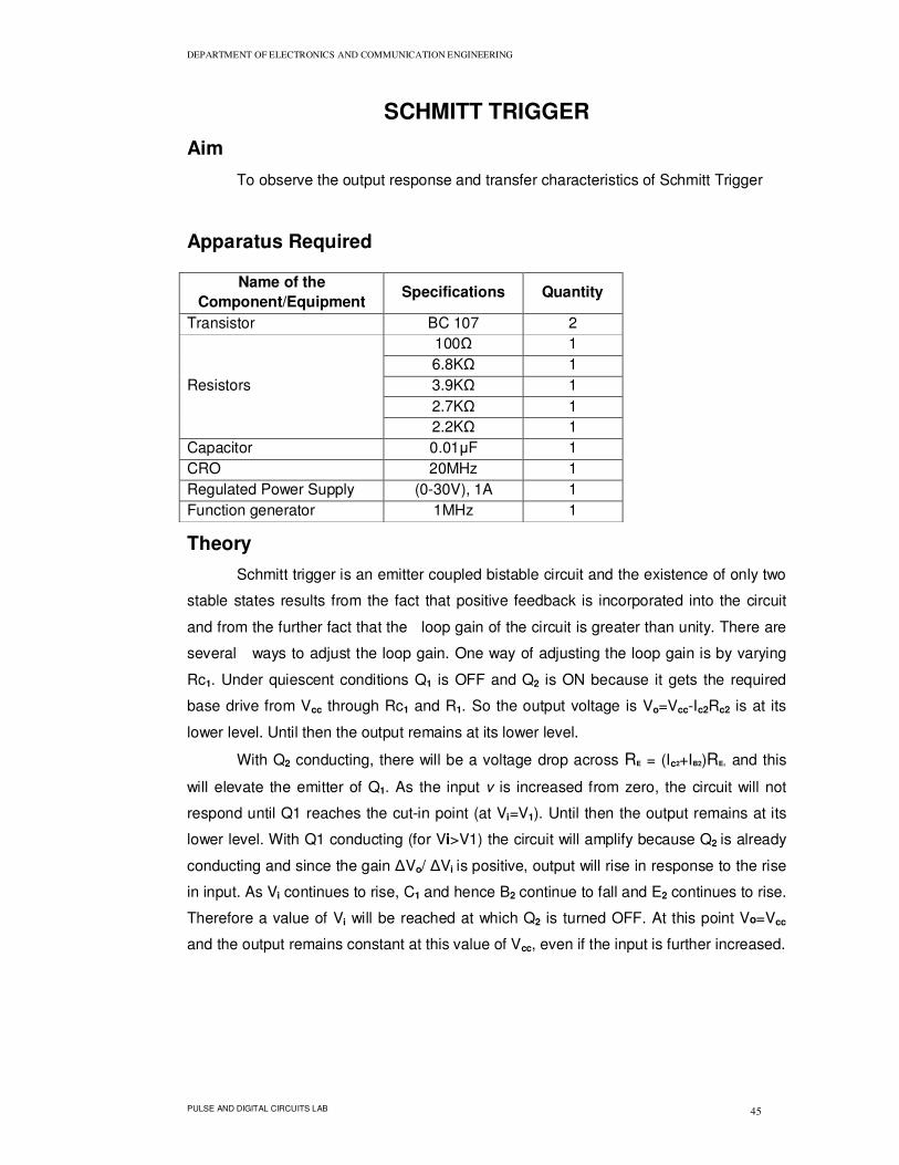
SCHMITT TRIGGER
Aim
To observe the output response and transfer characteristics of Schmitt Trigger
Apparatus Required
Theory
Schmitt trigger is an emitter coupled bistable circuit and the existence of only two
stable states results from the fact that positive feedback is incorporated into the circuit
and from the further fact that the loop gain of the circuit is greater than unity. There are
several ways to adjust the loop gain. One way of adjusting the loop gain is by varying
Rc1. Under quiescent conditions Q1 is OFF and Q2 is ON because it gets the required
base drive from Vcc through Rc1 and R1. So the output voltage is Vo=Vcc-Ic2Rc2 is at its
lower level. Until then the output remains at its lower level.
With Q2 conducting, there will be a voltage drop across RE = (Ic2+IB2)RE, and this
will elevate the emitter of Q1. As the input v is increased from zero, the circuit will not
respond until Q1 reaches the cut-in point (at Vi=V1). Until then the output remains at its
lower level. With Q1 conducting (for Vi>V1) the circuit will amplify because Q2 is already
conducting and since the gain ∆Vo/ ∆Vi is positive, output will rise in response to the rise
in input. As Vi continues to rise, C1 and hence B2 continue to fall and E2 continues to rise.
Therefore a value of Vi will be reached at which Q2 is turned OFF. At this point Vo=Vcc
and the output remains constant at this value of Vcc, even if the input is further increased.
Name of the
Component/Equipment Specifications Quantity
Transistor BC 107 2
Resistors
100Ω 1
6.8KΩ 1
3.9KΩ 1
2.7KΩ 1
2.2KΩ 1
Capacitor 0.01µF 1
CRO 20MHz 1
Regulated Power Supply (0-30V), 1A 1
Function generator 1MHz 1
DEPARTMENT OF ELECTRONICS AND COMMUNICATION ENGINEERING
PULSE AND DIGITAL CIRCUITS LAB 46
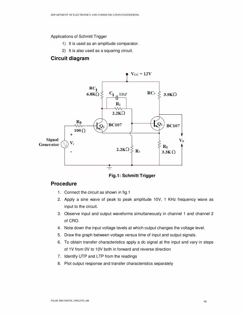
Applications of Schmitt Trigger
1) It is used as an amplitude comparator.
2) It is also used as a squaring circuit.
Circuit diagram
Fig.1: Schmitt Trigger
Procedure
1. Connect the circuit as shown in fig.1
2. Apply a sine wave of peak to peak amplitude 10V, 1 KHz frequency wave as
input to the circuit.
3. Observe input and output waveforms simultaneously in channel 1 and channel 2
of CRO.
4. Note down the input voltage levels at which output changes the voltage level.
5. Draw the graph between voltage versus time of input and output signals.
6. To obtain transfer characteristics apply a dc signal at the input and vary in steps
of 1V from 0V to 10V both in forward and reverse direction
7. Identify UTP and LTP from the readings
8. Plot output response and transfer characteristics separately
DEPARTMENT OF ELECTRONICS AND COMMUNICATION ENGINEERING
PULSE AND DIGITAL CIRCUITS LAB 47
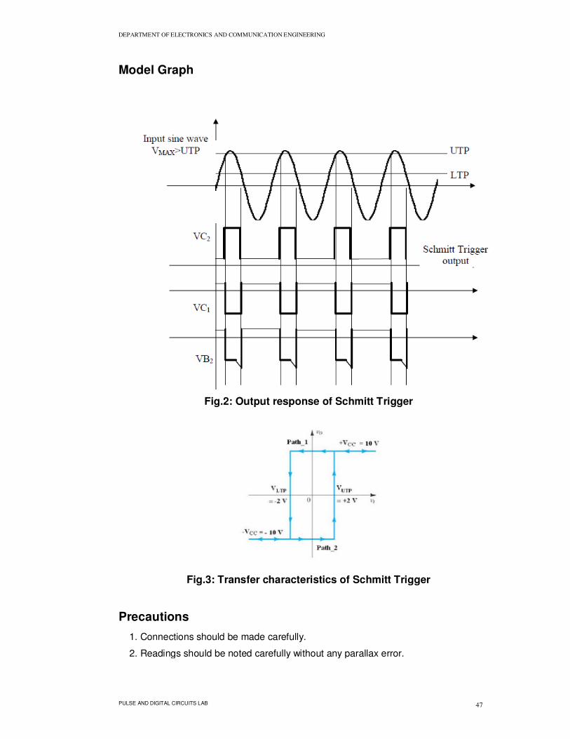
Model Graph
Fig.2: Output response of Schmitt Trigger
Fig.3: Transfer characteristics of Schmitt Trigger
Precautions
1. Connections should be made carefully.
2. Readings should be noted carefully without any parallax error.

DEPARTMENT OF ELECTRONICS AND COMMUNICATION ENGINEERING
PULSE AND DIGITAL CIRCUITS LAB 48
Result
Inference
Questions
1. What is the other name of the Schmitt trigger?
2. What are the applications of the Schmitt trigger?
3. Define the terms UTP & LTP?

DEPARTMENT OF ELECTRONICS AND COMMUNICATION ENGINEERING
PULSE AND DIGITAL CIRCUITS LAB 49
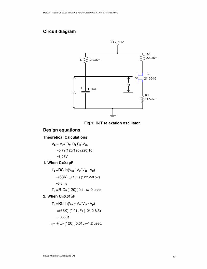
12. UJT RELAXATION OSCILLATOR
Aim
To observe the output response of UJT Relaxation Oscillator.
Apparatus Required
Name of the
Component/Equipment Specifications Quantity
UJT 2N 2646 1
Resistors
220Ω 1
68KΩ 1
120Ω 1
Capacitor
0.1µF 1
0.01µF 1
0.001µF 1
Diode 0A79 1
Inductor 130mH 1
CRO 20MHz 1
Function generator 1MHz 1
Regulated Power Supply (0-30V),1A 1
Theory
Many devices such as BJT, UJT, FET can be used as a switch. Here UJT is used
as a switch to obtain the sweep voltage. Capacitor C charges through the resistor, R
towards supply Voltage, Vbb. As long as the capacitor voltage is less than peak Voltage,
Vp, the emitter appears as an open circuit.
Vp =η Vbb + Vγ where,η = Intrinsic standoff ratio of UJT,
Vγ = Cut in voltage of diode.
When the capacitor voltage Vc exceeds voltage Vp, the UJT fires. The Capacitor starts
discharging through R1+Rb1. Where, Rb1 is the internal base resistance. As RB1 is
assumed negligible and hence capacitor discharges through R1.
Due to design of R1, this discharge is very fast, and is produces a pulse across R1.
When the capacitor voltage falls below Vv i.e. Vc=VE=Vv, the UJT gets turned OFF. The
capacitor starts charging again. This process is repeated until the power supply is
available.
DEPARTMENT OF ELECTRONICS AND COMMUNICATION ENGINEERING
PULSE AND DIGITAL CIRCUITS LAB 50
Circuit diagram
Fig.1: UJT relaxation oscillator
Design equations
Theoretical Calculations
Vp = Vγ+(R1/ R1 R2 )Vbb
=0.7+(120/120+220)10
=8.57V
1. When C=0.1µF
Tc =RC ln(Vbb- Vv/ Vbb- Vp)
=(68K) (0.1µF) (12/12-8.57)
=3.6ms
Td =R1C=(120)( 0.1µ)=12 µsec
2. When C=0.01µF
Tc =RC ln(Vbb- Vv/ Vbb- Vp)
=(68K) (0.01µF) (12/12-8.5)
= 365µs
Td =R1C=(120)( 0.01µ)=1.2 µsec.
DEPARTMENT OF ELECTRONICS AND COMMUNICATION ENGINEERING
PULSE AND DIGITAL CIRCUITS LAB 51
3. When C=0.001µF
Tc =RC ln(Vbb- Vv/ Vbb- Vp)
=(68K) (0.001µF) (12/12-8.5)
= 36.5µs
Td =R1C=(120)( 0.01µ)=0.12 µsec
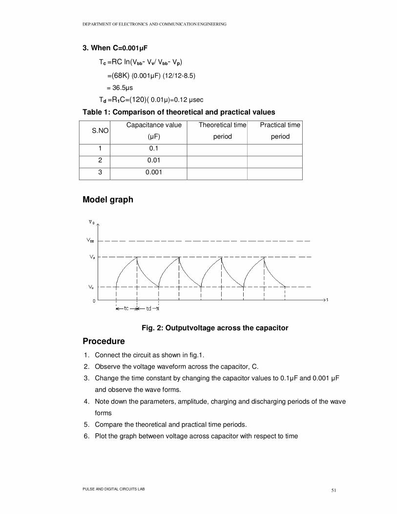
Table 1: Comparison of theoretical and practical values
S.NO Capacitance value
(µF)
Theoretical time
period
Practical time
period
1 0.1
2 0.01
3 0.001
Model graph
Fig. 2: Outputvoltage across the capacitor
Procedure
1. Connect the circuit as shown in fig.1.
2. Observe the voltage waveform across the capacitor, C.
3. Change the time constant by changing the capacitor values to 0.1µF and 0.001 µF
and observe the wave forms.
4. Note down the parameters, amplitude, charging and discharging periods of the wave
forms
5. Compare the theoretical and practical time periods.
6. Plot the graph between voltage across capacitor with respect to time

DEPARTMENT OF ELECTRONICS AND COMMUNICATION ENGINEERING
PULSE AND DIGITAL CIRCUITS LAB 52
Precautions
1. Connections should be given carefully.
2. Readings should be noted without parallox error.
Result
Inference
Questions
1. What do you mean by a) voltage time base generator, b) a current time bas generator.
2. What are the applications of time base generator?
3. What are the methods of generating a time base waveform?
DEPARTMENT OF ELECTRONICS AND COMMUNICATION ENGINEERING
PULSE AND DIGITAL CIRCUITS LAB 53
13. BOOT STRAP SWEEP CIRCUIT
Aim
To observe the output response of a boot strap sweep circuit.
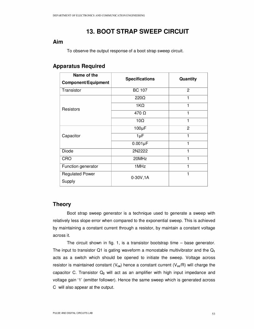
Apparatus Required
Name of the
Component/Equipment Specifications Quantity
Transistor BC 107 2
Resistors
220Ω 1
1KΩ 1
470 Ω 1
10Ω 1
Capacitor
100µF 2
1µF 1
0.001µF 1
Diode 2N2222 1
CRO 20MHz 1
Function generator 1MHz 1
Regulated Power
Supply 0-30V,1A
1
Theory
Boot strap sweep generator is a technique used to generate a sweep with
relatively less slope error when compared to the exponential sweep. This is achieved
by maintaining a constant current through a resistor, by maintain a constant voltage
across it.
The circuit shown in fig. 1, is a transistor bootstrap time – base generator.
The input to transistor Q1 is gating waveform a monostable multivibrator and the Q1
acts as a switch which should be opened to initiate the sweep. Voltage across
resistor is maintained constant (Vce) hence a constant current (Vcc/R) will charge the
capacitor C. Transistor Q2 will act as an amplifier with high input impedance and
voltage gain ‘1’ (emitter follower). Hence the same sweep which is generated across
C will also appear at the output.
DEPARTMENT OF ELECTRONICS AND COMMUNICATION ENGINEERING
PULSE AND DIGITAL CIRCUITS LAB 54
Circuit diagram
Fig. 1: Bootstrap sweep circuit
Wave forms
Fig. 2: Output response of Bootstrap sweep circuit
DEPARTMENT OF ELECTRONICS AND COMMUNICATION ENGINEERING
PULSE AND DIGITAL CIRCUITS LAB 55
Design equations
TS (max)=RC
Assume ‘C’ and find ‘R’ for given maximum sweep
Select Rb to provide enough bias for switching transistor Q1
Procedure
1. Connect the circuit as shown in the fig.1.
2. Apply the square wave input to the circuit (which is generated in the module itself).
3. Observe the output wave form.
4. By varying the input frequency observe the variations in the output.
5. Note the maximum value of sweep and starting voltage.
6. Note the sweep time Ts.
Result
Inference
Questions
1 .What are the other methods of sweep generator?
2. Compare bootstrap and miller sweep generator?

DEPARTMENT OF ELECTRONICS AND COMMUNICATION ENGINEERING
PULSE AND DIGITAL CIRCUITS LAB 56
ADDITIONAL EXPERIMENTS
1. ATTENUATORS
Aim
To design an attenuator circuit and observe different types of compensations
for different values of capacitors.
Apparatus Required
Name of the
Component/Equipment Specifications Quantity
Resistor 1kΩ 2
Capacitor 0.1µF, 0.01µF, 1µF 2
CRO 20MHz 1
Function generator 1MHz 1
Regulated Power Supply
(0-30)V,1A
1
Theory
Attenuators are resistive networks, which are used to reduce the amplitude of
the input signal. The simple resistor combination if Fig.1 in the circuit diagram would
multiply the input signal by the ratio 21
2
RR
R
+=α independently of the frequency. If the
output of the attenuator is feeding a stage of amplification , the input capacitance C2
of the amplifier will be the stray capacitance shunting the resistor R2 of the attenuator
and the attenuator will be as shown in Figure. And the attenuation now is not
independent of frequency.
Circuit Diagram
Fig. 1: Simple Attenuator
DEPARTMENT OF ELECTRONICS AND COMMUNICATION ENGINEERING
PULSE AND DIGITAL CIRCUITS LAB 57
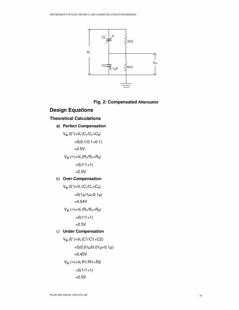
Fig. 2: Compensated Attenuator
Design Equations
Theoretical Calculations
a) Perfect Compensation
Vo (0+)=Vi (C1/C1+C2)
=5(0.1/0.1+0.1)
=2.5V
Vo (∞)=Vi (R1/R1+R2)
=5(1/1+1)
=2.5V
b) Over Compensation
Vo (0+)=Vi (C1/C1+C2)
=5(1µ/1µ+0.1µ)
=4.54V
Vo (∞)=Vi (R1/R1+R2)
=5(1/1+1)
=2.5V
c) Under Compensation
Vo (0+)=Vi (C1/C1+C2)
=5(0.01µ/0.01µ+0.1µ)
=0.45V
Vo (∞)=Vi R1/R1+R2
=5(1/1+1)
=2.5V

DEPARTMENT OF ELECTRONICS AND COMMUNICATION ENGINEERING
PULSE AND DIGITAL CIRCUITS LAB 58
Procedure
1. Connect the circuit diagram as shown in fig.1
2. Apply input voltage, VPP from the function generator to the circuit.
3. Observe the output wave form and note down the parameters
4. Connect the circuit diagram as shown in fig.2
5. Apply input voltage, VPP from the function generator to the circuit.
6. Keep the value of C1 = 0.1µF constant.
7. Now keep the value of C1 at 0.1µF for perfect compensation, at 1µF for over
compensation and at 0.01µF for under compensation.
8. Observe the output waveforms for each case and note down the values of
V0( ∞ ) and V0 (o+).
9. Compare the theoretical and practical values of each case.
10. Draw the graphs for perfect, over and under compensation network.
Model Graphs
Fig. 3: Perfect Compensation
Fig. 4: Over Compensation

DEPARTMENT OF ELECTRONICS AND COMMUNICATION ENGINEERING
PULSE AND DIGITAL CIRCUITS LAB 59
Fig. 5: Under Compensation
Precautions
1. Check the connections before giving the power supply
2. Observations should be done carefully
Result
Inference
Questions
1. What is the purpose of C1
2. What is the condition for perfect compensation?

DEPARTMENT OF ELECTRONICS AND COMMUNICATION ENGINEERING
PULSE AND DIGITAL CIRCUITS LAB 60
APPENDIX
Name of The Component
Specifications/Pin Diagrams
Transistor (BC 107)
* operating point temp-65o to 200o
* IC(max)= 0.2 Amp
* hfe (min) = 40
* hfe (max) = 450
Uni Junction Transistor (2N2646)
Ic 2.0A(Pulsed)
Vce 30V
PDISS 300mW@TC=25ºC
TSTG -65ºC to +150ºC
TJ -65ºC to +125ºC
өJC 33ºC/W
Diodes Type No 1N4001 1N4007
Max. Peak Inverse Volts 50 1000
Max RMS Supply Volts 35 700 Maximum Forward Voltage @ 1Ampere, DC @ 750 C
1.1 Volts,Peak
Maximum Reverse DC Current @PIV @ 250 C
10µA
Maximum Dynamic Reverse Current @PIV @750 C
30µA,Average

DEPARTMENT OF ELECTRONICS AND COMMUNICATION ENGINEERING
PULSE AND DIGITAL CIRCUITS LAB 61
REFERENCES 1. “Pulse and digital circuits”- J.Milliman and H.Taub, McGraw-Hill
2. “Solid State Pulse circuits”-David A.Bell, PHI
3. “Pulse and Digital Circuits”-A.Anand Kumar, PHI
4. www.analog.com/pdc
5. www.datasheetarchive.com
6. www.ti.com
![ARM-based Flash MCU - produktinfo.conrad.com · 128-Byte RX UART1 PDC Real-time Events PIO High Speed MCI DMA PDC PDC PDC PDC Timer Counter A TC[0..2] UART0 TWCK0 TWD0 TWD1 UTXD0](https://static.fdocuments.us/doc/165x107/5c387e4109d3f23f308b764d/arm-based-flash-mcu-128-byte-rx-uart1-pdc-real-time-events-pio-high-speed.jpg)