WITHIN THE ERP SYSTE M 00136 A - vectron.com · Control Voltage Range (Vc): ... Devices are handled...
19
REV DESCRIPTION DATE PREP APPD B CO-28749 1/31/18 DF/SM HW Oscillator Specification, Hybrid VCSO For MOUNT HOLLY SPRINGS, PA 17065 Hi-Rel Standard, LVPECL Output THE RECORD OF APPROVAL FOR THIS DOCUMENT IS MAINTAINED ELECTRONICALLY WITHIN THE ERP SYSTEM CODE IDENT NO SIZE DWG. NO. REV 00136 A DOC206906 B UNSPECIFIED TOLERANCES: N/A SHEET 1 0F 19 MICROSEMI PROPRIETARY
Transcript of WITHIN THE ERP SYSTE M 00136 A - vectron.com · Control Voltage Range (Vc): ... Devices are handled...
REV DESCRIPTION DATE PREP APPD
B CO-28749 1/31/18 DF/SM HW
Oscillator Specification, Hybrid VCSO For
MOUNT HOLLY SPRINGS, PA 17065 Hi-Rel Standard, LVPECL Output
THE RECORD OF APPROVAL FOR THIS
DOCUMENT IS MAINTAINED ELECTRONICALLY
WITHIN THE ERP SYSTEM
CODE IDENT NO SIZE DWG. NO. REV
00136 A DOC206906 B
UNSPECIFIED TOLERANCES: N/A SHEET 1 0F 19
MICROSEMI PROPRIETARY

SIZE CODE IDENT NO.
UNSPECIFIED TOLERANCES DWG NO. REV. SHEET
A 00136 N/A DOC206906 B 2 VECTRON INTERNATIONAL PROPRIETARY
1. SCOPE
1.1 General. This specification defines the design, assembly and functional evaluation of high
reliability, hybrid voltage controlled SAW oscillators produced by Microsemi. Devices
delivered to this specification represent the standardized Parts, Materials and Processes (PMP)
Program developed, implemented and certified for advanced applications and extended
environments.
1.2 Applications Overview. The designs represented by these products were primarily developed
for the MIL-Aerospace community. The lesser Design Pedigrees and Screening Options
imbedded within DOC206906 bridge the gap between Space and COTS hardware by providing
custom hardware with measures of mechanical, assembly and reliability assurance needed for
Military or Ruggedized COTS environments.
2. APPLICABLE DOCUMENTS
2.1 Specifications and Standards. The following specifications and standards form a part of this
document to the extent specified herein. The issue currently in effect on the date of quotation
will be the product baseline, unless otherwise specified. In the event of conflict between the
texts of any references cited herein, the text of this document shall take precedence.
Military
MIL-PRF-55310 Oscillators, Crystal Controlled, General Specification For
MIL-PRF-38534 Hybrid Microcircuits, General Specification For
Standards
MIL-STD-202 Test Method Standard, Electronic and Electrical Component Parts
MIL-STD-750 Test Method Standard, Test Methods for Semiconductor Devices
MIL-STD-883 Test Methods and Procedures for Microelectronics
Other
QSP-90100 Quality Systems Manual, Microsemi
DOC007131 Identification Common Documents, Materials and Processes, Hi-Rel XO
DOC203982 DPA Specification
QSP-91502 Procedure for Electrostatic Discharge Precautions
3. GENERAL REQUIREMENTS
3.1 Classification. All devices delivered to this specification are of hybrid technology conforming
to Class 2 of MIL-PRF-55310. Primarily developed as a Class S equivalent specification,
options are imbedded within it to also produce Class B, Engineering Model and Ruggedized
COTS devices. Devices carry a Class 1B ESDS classification per MIL-PRF-38534.
3.2 Item Identification. Unique model number series are utilized to identify device package
configurations as listed in Table 1.

SIZE CODE IDENT NO.
UNSPECIFIED TOLERANCES DWG NO. REV. SHEET
A 00136 N/A DOC206906 B 3 VECTRON INTERNATIONAL PROPRIETARY
3.3 Absolute Maximum Ratings.
a. Supply Voltage Range (VCC): 0Vdc to +6.0Vdc
b. Control Voltage Range (Vc): -0.5Vdc to +8.0Vdc
c. Storage Temperature Range (TSTG): -55°C to +125°C
d. Junction Temperature (TJ): +150°C
e. Lead Temperature (soldering, 10 seconds): +300°C
3.4 Design, Parts, Materials and Processes, Assembly, Inspection and Test.
3.4.1 Design. The ruggedized designs implemented for these devices are proven in military and
space applications under extreme environments. Designs utilize Established Reliability (MIL-
ER) components where possible. When specified, radiation hardening up to 50krad (Si) (RHA
level L) is met by utilizing active device lots that have passed testing to that level.
3.4.1.1 Design and Configuration Stability. Barring changes to improve performance by reselecting
passive chip component values to offset component tolerances, there will not be fundamental
changes to the design or assembly or parts, materials and processes after first product delivery
of that item without written approval from the procuring activity.
3.4.1.2 Environmental Integrity. Designs have passed the environmental qualification levels of MIL-
PRF-55310. These designs have also passed extended dynamic levels of at least:
a. Sine Vibration: MIL-STD-202, Method 204, Condition G (30g pk.)
b. Random Vibration: MIL-STD-202, Method 214, Condition II-J (43.92g rms, three
minute duration in each of three mutually perpendicular directions)
c. Mechanical Shock: MIL-STD-202, Method 213, Condition F (1500g, 0.5ms)
3.4.2 Prohibited Parts, Materials and Processes. The items listed are prohibited for use in high
reliability devices produced to this specification.
a. Gold metallization of package elements without a barrier metal.
b. Zinc chromate as a finish.
c. Cadmium, zinc, or pure tin external or internal to the device.
d. Plastic encapsulated semiconductor devices.
e. Ultrasonically cleaned electronic parts.
f. Heterojunction Bipolar Transistor (HBT) technology.
3.4.3 Assembly. Manufacturing utilizes standardized procedures, processes and verification
methods to produce MIL-PRF-55310 Class S / MIL-PRF-38534 Class K equivalent devices.
MIL-PRF-38534 Group B Option 1 in-line inspection is included on radiation hardened part
numbers to further verify lot pedigree. Traceability of all components and production lots are
in accordance with MIL-PRF-38534, as a minimum. Tabulated records are provided as a part
of the deliverable data package. Devices are handled in accordance with Microsemi document
QSP-91502 (Procedure for Electrostatic Discharge Precautions).
3.4.4 Inspection. The inspection requirements of MIL-PRF-55310 apply to all devices delivered to
this document. Inspection conditions and standards are documented in accordance with the
Quality Assurance, ISO-9001 and AS9100 derived, System of QSP-90100.

SIZE CODE IDENT NO.
UNSPECIFIED TOLERANCES DWG NO. REV. SHEET
A 00136 N/A DOC206906 B 4 VECTRON INTERNATIONAL PROPRIETARY
3.4.5 Test. The Screening test matrix of Table 5 is tailored for selectable-combination testing to
eliminate costs associated with the development/maintenance of device-specific documentation
packages while maintaining performance integrity.
3.4.6 Marking. Device marking shall be in accordance with the requirements of MIL-PRF-55310.
3.4.7 Ruggedized COTS Design Implementation. Design Pedigree “D” devices (see ¶ 5.2) use the
same robust designs found in the other device pedigrees. They do not include the provisions of
traceability or the Class-qualified components noted in paragraphs 3.4.3 and 4.1.
4. DETAIL REQUIREMENTS
4.1 Components
4.1.1 Resonators. VCSO designs utilize a Surface Acoustic Wave (SAW) resonator as the frequency
determining device. The SAW is manufactured and sealed in its own package prior to
mounting in the hybrid. Resonators used in flight models will come from lots that have passed
MIL-PRF-38534 Lot Acceptance Test for SAW devices plus 100% screening and electrical
test prior to installation into the VCSO.
4.1.2 Passive Components. Passive components will have the same pedigree as the die specified in
paragraph 7.1. When required, established Reliability (ER) failure level R minimum passive
components are procured from QPL suppliers where possible. Lot evaluations are in
accordance with MIL-PRF-38534 or Enhanced Element Evaluation as specified in Table 8.
When used, inductors may be open construction and may use up to 47 gauge wire.
4.1.3 Class S/K Active Devices. Active devices are procured from wafer lots that have passed MIL-
PRF-38534 Lot Acceptance Tests for Class K devices. When optionally specified, further
testing in accordance with MIL-PRF-55310 and MIL-PRF-38534 is performed for radiation
hardness assurance (excluding varactor diodes) and for Enhanced Element Evaluation as
specified in Tables 6 and 7. Varactor diodes are considered radiation tolerant by design. The
LVPECL microcircuit used in this design is certified for 50krad (Si) ELDRS.
4.1.3.1 Class B Active Devices. When specified, active devices assembled into DOC206906 design
pedigree “B” devices (¶ 5.2a) are procured from wafer lots that have passed MIL-PRF-55310
element evaluations for Class B devices.
4.1.4 Packages. Packages are procured that meet the construction, lead materials and finishes as
specified in MIL-PRF-55310. All leads are Kovar with gold plating over a nickel underplate.
Package lots are upscreened in accordance with the requirements of MIL-PRF-38534 as
applicable.
4.1.5 Traceability and Homogeneity. All design pedigrees except option D have active device lots
that are traceable to the manufacturer’s individual wafer; all other elements and materials are
SIZE CODE IDENT NO.
UNSPECIFIED TOLERANCES DWG NO. REV. SHEET
A 00136 N/A DOC206906 B 5 VECTRON INTERNATIONAL PROPRIETARY
traceable to their manufacturer and incoming inspection lots. Design pedigrees E and R have
homogenous material.
4.1.6 Enhanced Element Evaluation. When Design Pedigree Option “E” is specified, active and
passive devices with Enhanced Element Evaluation as listed in Table 6, 7 and 8 shall be
implemented for the highest reliability preference.
4.2 Mechanical.
4.2.1 Package Outline. See Table.
4.2.2 Thermal Characteristics. Because these VCSO’s are multichip hybrid designs, the actual θjc to
any one given semiconductor die will vary, but the combined average for all active devices
results in a θjc of approximately 90°C/W. The typical die temperature rise at any one given
semiconductor is 8°C to 14°C. With the oscillator operating at +85°C, the average junction
temperature is approximately +99°C and under no circumstance will it ever exceed the
maximum manufacturer’s rated junction temperature.
4.2.3 Weight. 3.5 grams typical
4.3 Electrical.
4.3.1 Input Power. Devices are designed for standard +3.3Vdc operation, ±5%.
4.3.2 Temperature Range. Operating range is -40°C to +85°C.
4.3.3 Absolute Pull Range. Absolute pull range is defined as the minimum guaranteed amount the
VCXO can be varied, about the center frequency (fo). It accounts for degradations including
initial frequency tolerance, temperature stability (-40 to 85°C), aging (15 years), radiation
effects, power supply variations (±5%) and load variations (±10%).
4.3.4 Frequency Aging. When tested in accordance with MIL-PRF-55310 Group B inspection, the
15-year aging projection shall not cause the minimum APR limit to be exceeded.
4.3.5 All devices include an External Frequency Control (EFC) pin for the purpose of externally
setting each VCSO to its nominal frequency.
4.3.6 Output Load. 50Ω to Vcc-2.0V (each output)
5. QUALITY ASSURANCE PROVISIONS AND VERIFICATION
5.1 Verification and Test. Device lots shall be tested prior to delivery in accordance with the
applicable Screening Option letter as stated by the 15th
character of the part number. Table 5
tests are conducted in the order shown and annotated on the appropriate process travelers and
data sheets of the governing test procedure. For devices that require Screening Options that
SIZE CODE IDENT NO.
UNSPECIFIED TOLERANCES DWG NO. REV. SHEET
A 00136 N/A DOC206906 B 6 VECTRON INTERNATIONAL PROPRIETARY
include MIL-PRF-55310 Group A testing, the Post-Burn-In Electrical Test and the Group A
Electrical Test are combined into one operation.
5.1.1 Screening Options. The Screening Options, by letter, are summarized as:
A Modified MIL-PRF-38534 Class K
B Modified MIL-PRF-55310 Class B Screening & Group A Quality Conformance
Inspection (QCI)
C Modified MIL-PRF-55310 Class S Screening & Group A QCI
D Modified MIL-PRF-38534 Class K with Group B Aging
E Modified MIL-PRF-55310 Class B Screening, Groups A & B QCI
F Modified MIL-PRF-55310 Class S Screening, Groups A & B QCI
G Modified MIL-PRF-55310 Class B Screening & Post Burn-in Nominal
Electricals
X Engineering Model (EM)
5.2 Optional Design, Test and Data Parameters. The following is a list of design, assembly,
inspection and test options that can be selected or added by purchase order request.
a. Design Pedigree (choose one as the 5th
character in the part number):
(E) Enhanced Element Evaluation, 50krad Class K die
(R) Hi-Rel design w/ 50krad Class K die
(B) Hi-Rel design w/ Class B die
(D) Hi-Rel design w/ commercial grade components
b. Input Voltage, (A) for +3.3V as the 14th
character
c. Radiographic Inspection
d. Group C Inspection: MIL-PRF-55310 (requires 8 destruct specimens)
e. Group C Inspection: MIL-PRF-38534, Table C-Xc, Condition PI [requires 8 destruct
specimens – Life (5), RGA (3)]. Subgroup 1 fine leak test to be performed per
MIL-STD-202, Method 112, Condition C.
f. Qualification: In accordance with EEE-INST-002, Section C4, Table 3, Level 1 or 2
(requires 11 destruct specimens)
g. Qualification: In accordance with MIL-PRF-55310, Table IV (requires 11 destruct
specimens).
g. Internal Water-Vapor Content (RGA) samples and test performance
h. MTBF Reliability Calculations
i. Worst Case/Derating Analysis (MIL-HDBK-1547) with Tj Max = +105°C;
Derated Maximum Operating Temp = Tj Max - ∆Tj
j. Deliverable Process Identification Documentation (PID)
k. Customer Source Inspection (pre-cap / final)
l. Destruct Physical Analysis (DPA): MIL-STD-1580 with exceptions as specified in
Microsemi DOC203982.
m. High Resolution Digital Pre-Cap Photographs (20 Megapixels minimum)
n. Hot solder dip of leads with Sn63/Pb37 solder prior to shipping.
5.2.1 NASA EEE-INST-002. A combination of Design Pedigree E or R, Option F Screening, Group
C Inspection in accordance with Table VII of MIL-PRF-55310 and RGA, meet the
requirements of Level 1 device reliability. A combination of Design Pedigree B, Option E

SIZE CODE IDENT NO.
UNSPECIFIED TOLERANCES DWG NO. REV. SHEET
A 00136 N/A DOC206906 B 7 VECTRON INTERNATIONAL PROPRIETARY
Screening, Radiographic Inspection, Group C Inspection in accordance with Table VII of MIL-
PRF-55310 and RGA, meet the requirements of Level 2 device reliability.
5.3 Test Conditions. Unless otherwise stated herein, inspections are performed in accordance with
those specified in MIL-PRF-55310 and MIL-PRF-38534, in that order. Process travelers
identify the applicable methods, conditions and procedures to be used. Examples of electrical
test procedures that correspond to MIL-PRF-55310 requirements are shown in Table 3.
5.4 Deliverable Data. The manufacturer supplies the following data, as a minimum, with each lot
of devices:
a. Completed assembly and screening lot travelers, including rework history and Certificate
of Conformance.
b. Electrical test variables data, identified by unique serial number.
c. Frequency-Temperature Data, Radiographic films, Group C data and RGA data as
required by purchase order.
d. Traceability, component LAT, enclosure LAT and RLAT (if specifically requested on
the purchase order).
5.5 Discrepant Material. All MRB authority resides with the procuring activity.
5.6 Failure Analysis. Any catastrophic failure (no clocking, no current) at Post Burn-In or after
will be evaluated for root cause. The customer will be notified after occurrence and upon
completion of the evaluation.
6. PREPARATION FOR DELIVERY
6.1 Packaging. Devices will be packaged in a manner that prevents handling, ESD and
transit damage during shipping.

SIZE CODE IDENT NO.
UNSPECIFIED TOLERANCES DWG NO. REV. SHEET
A 00136 N/A DOC206906 B 8 VECTRON INTERNATIONAL PROPRIETARY
7. ORDERING INFORMATION
7.1 Ordering Part Number. The ordering part number is made up of an alphanumeric series
of 15 characters. Design-affected product options, identified by the parenthetic letter on
the Optional Parameters list (¶ 5.2a and b), are included within the device part number.
The Part Number breakdown is described as:
6304 R 1G000000 A F
7.1.1 Model Number. The device model number is the four (4) digit number assigned to a
corresponding package and output combination per Table 1.
7.1.2 Design Pedigree. Class S variants correspond to either letter “E” or “R” and are described in
paragraph 5.2a. The Class B variant corresponds to letter “B” and is described in paragraph
5.2a. Ruggedized COTS, using commercial grade components, corresponds to letter “D”.
7.1.3 Output Frequency. The nominal output frequency is expressed in the format as specified in
MIL-PRF-55310 utilizing eight (8) characters.
Model # (Table 1)
Design Pedigree
E = Enhanced Element Evaluation,
50krad, Class S/K Die
R = 50krad Class S/K Die
B = Class B Die
D = Ruggedized COTS:
Commercial Grade
Components
Screening Option
per Table 5, 5.1.1
Input Voltage
A = +3.3V
Frequency
SIZE CODE IDENT NO.
UNSPECIFIED TOLERANCES DWG NO. REV. SHEET
A 00136 N/A DOC206906 B 9 VECTRON INTERNATIONAL PROPRIETARY
7.1.4 Input Voltage. Voltage is the 14th
character, letter “A” = represents +3.3V.
7.1.5 Screening Options. The 15th
character is the Screening Option (letter A thru G or X) selected
from Table 5.
7.2 Optional Design, Test and Data Parameters. Test and documentation requirements above that
of the standard high reliability model shall be specified by separate purchase order line items
(as listed in ¶ 5.2c thru n).
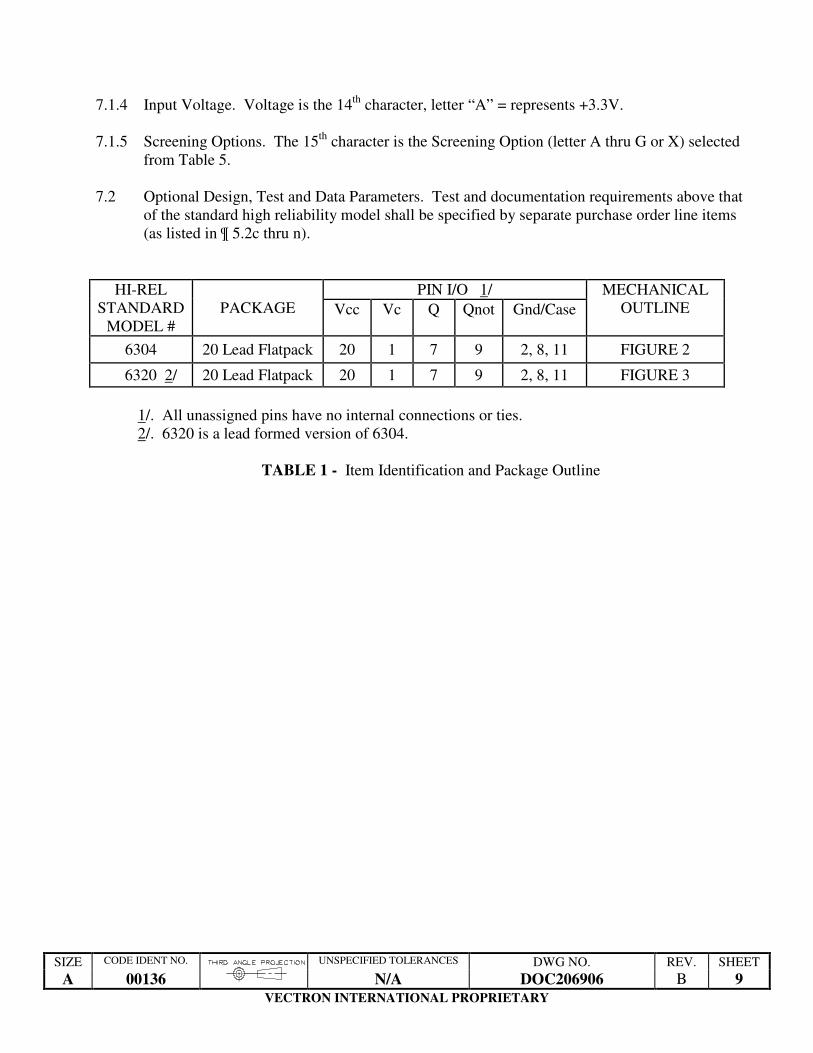
HI-REL
STANDARD
MODEL #
PACKAGE
PIN I/O 1/ MECHANICAL
OUTLINE Vcc Vc Q Qnot Gnd/Case
6304 20 Lead Flatpack 20 1 7 9 2, 8, 11 FIGURE 2
6320 2/ 20 Lead Flatpack 20 1 7 9 2, 8, 11 FIGURE 3
1/. All unassigned pins have no internal connections or ties.
2/. 6320 is a lead formed version of 6304.
TABLE 1 - Item Identification and Package Outline

SIZE CODE IDENT NO.
UNSPECIFIED TOLERANCES DWG NO. REV. SHEET
A 00136 N/A DOC206906 B 10 VECTRON INTERNATIONAL PROPRIETARY
Frequency
Range
(MHz)
Current,
No load
(mA max)
Rise / Fall
Time
(ps max.)
Duty Cycle
(%)
300 – 1000 65 900 40 to 60
TABLE 2 - Electrical Performance Characteristics
Nominal
Frequency
(MHz)
Typical Period Jitter
1 sigma
(ps)
Typical Period Jitter
peak-to-peak
(ps)
Phase Jitter
12kHz to 20MHz
(ps)
300 6 50 0.10
1000 2 16 0.05
TABLE 2A - Typical Jitter
Frequency Range: 300 MHz to 1.000 GHz
Temperature Range: -40°C to +85°C
Initial Tolerance: -50 ppm to +150 ppm typical
Frequency-Voltage Tolerance: ±5 ppm typical (Vcc ±5%)
Frequency Aging: ±30 ppm typical (projected over 15 years)
Supply Voltage: +3.3V ±5%
Absolute Pull Range: ±20 ppm min. (See paragraph 4.3.3)
Control Voltage (Vc) Range: 0 V to +3.3V
Input Impedance: 100kΩ min.
Modulation Bandwidth: 100kHz min.( Fo ≥ 500MHz), 50kHz min.(Fo < 500MHz)
Slope: Positive
Linearity: ±10% max.
F vs. V Gain: 90 ppm/V typical
Output Voltage: VOH= Vcc-1.085 to Vcc-0.880, VOL=Vcc-1.830 to Vcc-1.555
Sub-Harmonics: None
Phase Noise: See Figure 1
SIZE CODE IDENT NO.
UNSPECIFIED TOLERANCES DWG NO. REV. SHEET
A 00136 N/A DOC206906 B 11 VECTRON INTERNATIONAL PROPRIETARY
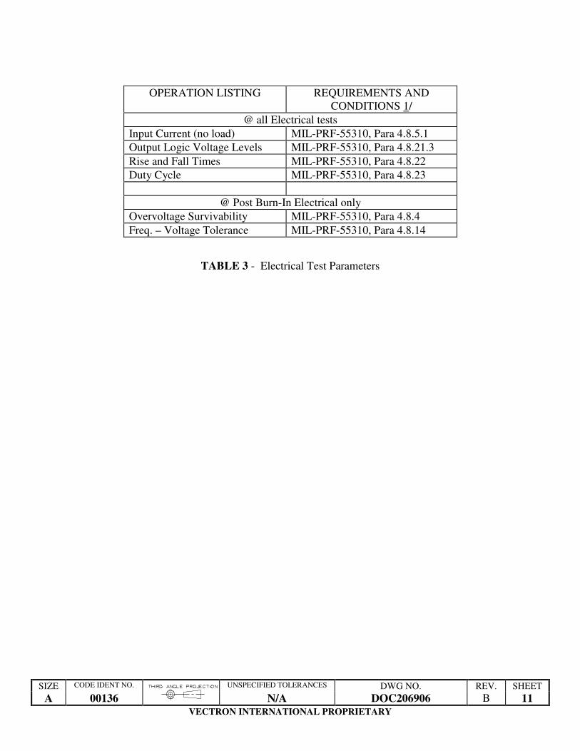
OPERATION LISTING REQUIREMENTS AND
CONDITIONS 1/
@ all Electrical tests
Input Current (no load) MIL-PRF-55310, Para 4.8.5.1
Output Logic Voltage Levels MIL-PRF-55310, Para 4.8.21.3
Rise and Fall Times MIL-PRF-55310, Para 4.8.22
Duty Cycle MIL-PRF-55310, Para 4.8.23
@ Post Burn-In Electrical only
Overvoltage Survivability MIL-PRF-55310, Para 4.8.4
Freq. – Voltage Tolerance MIL-PRF-55310, Para 4.8.14
TABLE 3 - Electrical Test Parameters

SIZE CODE IDENT NO.
UNSPECIFIED TOLERANCES DWG NO. REV. SHEET
A 00136 N/A DOC206906 B 12 VECTRON INTERNATIONAL PROPRIETARY
Figure 1A – Typical Phase Noise @ 300.000MHz

SIZE CODE IDENT NO.
UNSPECIFIED TOLERANCES DWG NO. REV. SHEET
A 00136 N/A DOC206906 B 13 VECTRON INTERNATIONAL PROPRIETARY
Figure 1B – Typical Phase Noise @ 1.000GHz
SIZE CODE IDENT NO.
UNSPECIFIED TOLERANCES DWG NO. REV. SHEET
A 00136 N/A DOC206906 B 14 VECTRON INTERNATIONAL PROPRIETARY
LEGEND: X = Required, NR = Not Required, AR = As Required
TABLE 5 - Test Matrix
1/ Performed at package LAT. Include LAT data sheet
2/ When specified, RGA samples will be removed from the lot after completion of this operation. Use of Screening failures require customer concurrence.
3/ By customer request, the Aging test may be terminated after 15 days if the measured aging rate is less than one-half the specified aging rate, as described in paragraph
4.3.4.1 herein. See the customer PO.
OPN.
NO.
OPERATION LISTING REQUIREMENTS AND CONDITIONS Option
A
Option
B
Option
C
Option
D
Option
E
Option
F
Option
G
Option
X
SCREENING MIL Class Similarity K
100%
B-
100%
S-
100%
K+
100%
B
100%
S
100%
100%
EM
100%
1 Non-Destruct Bond Pull MIL-STD-883, Meth 2023 X NR X X NR X NR NR
2 Internal Visual MIL-STD-883, Meth 2017 Class K,
Meth 2032 Class K
X X X X X X X X
3 Stabilization (Vacuum) Bake MIL-STD-883, Meth 1008, Cond C, 150°C X
48 hrs.
X
24 hrs.
X
48 hrs.
X
48 hrs.
X
24 hrs.
X
48 hrs.
X
24 hrs.
X
24 hrs.
4
Thermal Shock MIL-STD-883, Meth 1011, Cond A NR NR X NR NR X NR NR
5 Temperature Cycle MIL-STD-883, Meth 1010, Cond. B,
10 cycles min.
X X X X X X X NR
6 Constant Acceleration MIL-STD-883, Meth 2001, Cond A,
Y1 plane only, 5000 g’s
X X X X X X X NR
7 Particle Impact Noise Detection MIL-STD-883, Meth 2020, Cond B X X
X
X
X
X
NR X
8 Electrical Testing, Pre Burn-In
Perform tests in Table 3. Nominal Vcc, nominal
temperature
X X X X X X X X
9 1st Burn-In
MIL-STD-883, Meth 1015, Condition B X
160 hrs.
X
160 hrs.
X
240 hrs.
X
160 hrs.
X
160 hrs.
X
240 hrs.
X
160 hrs.
NR
10 Electrical Testing, Intermediate
Perform tests in Table 3. Nominal Vcc, nominal
temperature
X NR NR X NR NR NR NR
11 2nd Burn-In
MIL-STD-883, Meth 1015, Condition B X
160 hrs.
NR NR X
160 hrs.
NR NR NR NR
12 Electrical Testing, Post Burn-In
(Group A)
Perform tests in Table 3. Nominal Vcc & extremes,
nominal temperature & extremes
X X X X X X X
nom. Vcc
NR
13 Seal: Fine Leak MIL-STD-202, Meth 112, Cond C
5 x 10⁻⁸ atm cc/sec max
X X X X X X X X
14 Seal: Gross Leak MIL-STD-202, Meth 112, Cond D X X X X X X X X
15
Radiographic Inspection MIL-STD-883, Meth 2012 X AR AR X AR X NR NR
16 Solderability MIL-STD-883, Meth 2003 1/ 1/ 1/ 1/ 1/ 1/ 1/ NR
17 External Visual & Mechanical MIL-STD-883, Meth 2009 X 2/ X 2/ X 2/ X 2/ X 2/ X 2/ X 2/ X 2/
18
Aging, 30 Day 3/
(M55310 Group B)
MIL-PRF-55310, para. 4.8.35.1 NR NR NR X 13 pcs. X NR NR

SIZE CODE IDENT NO.
UNSPECIFIED TOLERANCES DWG NO. REV. SHEET
A 00136 N/A DOC206906 B 15 VECTRON INTERNATIONAL PROPRIETARY
Subgroup Class Test Mil-STD-883 Quantity
Mil-PRF-
38534
Reference
K Method Condition (accept number) Paragraph
1 X
Element Electrical A. May perform at wafer level
B. All failures shall be removed
from the lot
C. Perform at room ambient
100% C.3.3.1
2 X Element Visual 2010 100% C.3.3.2
3 X Internal Visual 2010 10(0) or 22(0)
(See Notes 1 & 2)
C.3.3.3
C.3.3.4.2
4 X Temperature Cycling 1010 C C.3.3.3
X Mechanical Shock
or
Constant Acceleration
2002
2001
B, Y1
direction
3,000 G, Y1
direction
10(0)
22(0)
(See Notes 1 & 2)
X Interim Electrical C.3.3.4.3
X Burn-In 1015
240 hours
minimum at
+125°C
X Post Burn-In Electrical C.3.3.4.3
X Steady State Life 1005
X Final Electrical C.3.3.4.3
5 X Wire Bond Evaluation 2011 10(0) wires or
20(1) wires
C.3.3.3
C.3.3.5
6 X SEM 2018 See method 2018
& Note 2 C.3.3.6
NOTES:
1. Subgroups 3, 4, & 5 shall be performed on a sample of 10 die if the wafer lot is from a QPL/QML line.
If the die are from commercial wafer lots, then the sample size shall be 22 die. Die from QPL/QML
wafers not meeting the QPL/QML requirements and downgraded to commercial grade shall not be used.
2. Subgroups 3, 4 & 5 shall be performed in the order listed in Table 1. Subgroup 6 may be performed at
any time.
TABLE 6: MICROCIRCUIT ENHANCED ELEMENT EVALUATION

SIZE CODE IDENT NO.
UNSPECIFIED TOLERANCES DWG NO. REV. SHEET
A 00136 N/A DOC206906 B 16 VECTRON INTERNATIONAL PROPRIETARY
Subgroup Class Test Mil-STD-750 Quantity
Mil-PRF-
38534
Reference
K Method Condition (accept number) Paragraph
1 X
Element Electrical A. May perform at wafer level
B. All failures shall be removed
from the lot
Perform at room
ambient 100% C.3.3.1
2 X Element Visual 2069, 2070,
2072, 2073 100% C.3.3.2
3 X Internal Visual 2069, 2070,
2072, 2073, 2074
10(0) or 22(0)
(Notes 1 & 2)
C.3.3.3
C.3.3.4.2
4 X Temperature Cycling 1051 C C.3.3.3
X Surge Current
(when applicable)
4066 A or B as
specified
X Constant Acceleration 2006
2001
Y1 direction
20,000 G /
10,000 G for
Pd ≥ 10W
10(0)
22(0)
(See Notes 1 & 2)
X Interim Electrical C.3.3.4.3
X High Temperature
Reverse Bias (HTRB)
1039
1042
1038
A
B
A
X Interim Electrical & Delta
Complete
Within 16 hrs of
HTRB
completion
X Burn-In 240 hours
1039, 1042
1038
1040
B, A
B
X Post Burn-In Electrical C.3.3.4.3
X
Steady State Life
1000 hours or equivalent
per MIL-PRF-19500
1026
1037
1042
1048
X Final Electrical C.3.3.4.3
5 X Wire Bond Evaluation 2011 10(0) wires or
20(1) wires
C.3.3.3
C.3.3.5
6 X SEM 2018
2077
See method 2018
or 2077 & Note 2 C.3.3.6
TABLE 7: SEMICONDUCTOR ENHANCED ELEMENT EVALUATION

SIZE CODE IDENT NO.
UNSPECIFIED TOLERANCES DWG NO. REV. SHEET
A 00136 N/A DOC206906 B 17 VECTRON INTERNATIONAL PROPRIETARY
Part Type Test Requirements
Paragraph Sample Size Allowable Rejects
Ceramic capacitors (Production lot definition shall be per M55681 or M123 for chips, or M49470 T-level for stacks)
M55681 FRL S or M123
(chips) N/A N/A N/A N/A
DSCC Dwg COTS (chips) Ultrasonic scan or CSAM M123 100% N/A
Group A M123 M123 M123
Group B, Subgroups 1 &
2 M123 M123 M123
T-level M49470 (stacked) N/A N/A N/A N/A
General purpose M49470, Ultrasonic scan or CSAM M49470 for T-level 100% N/A
DSCC dwg or COTS Group A M49470 for T-level M49470 for T-level M49470 for T-level
(stacked) Group B, Subgroups 2, 4
& 5b M49470 for T-level M49470 for T-level M49470 for T-level
Tantalum Chip Capacitors (Note: Stacking tantalum chips will require a repeat of the entire Group A in M55365 with
minimum Weibull C and surge current option C. Production lot definition shall be per M55365.)
M55365
Group A (Weibull C
minimum with surge
current option C)
M55365 M55365 M55365
DSCC Dwg, COTS
Group A (Weibull C
minimum with surge
current option C)
M55365 M55365 M55365
Group C M55365 M55365 M55365
Resistor Chips (Note: Gluing one resistor chip on top of another to change a design or save on real estate is not allowable
without extensive design/process verification, long term testing, and hybrid re-qualification. Production lot definition shall be
per M55342).
M55342 FRL R or S N/A N/A N/A N/A
DSCC Dwg, COTS Group A M55342 for T-level M55342 for T-level M55342 for T-level
Group B M55342 for T-level M55342 for T-level M55342 for T-level
Inductors (See Paragraph 4.1.2)
Magnetics, Closed Construction Leaded and Surface Mount (transformers, inductors, coils) (Note: Stacking magnetics shall be
qualified and the effects of the long term performance of the hybrids verified. When stacking magnetics, a repeat of the thermal
cycling plus electrical measurements as specified in Group A of Mil-Std-981. Design, workmanship and materials/processes
shall conform to MIL-STD-981 requirements).
Magnetics, Open Construction are unencapsulated and unpotted self-leaded parts consisting of magnet wire wound around a
magnetic core. These parts are fully visually inspectable. Open construction magnetics shall be subjected to 100% electrical
measurements and visual inspection per Mil-Std-981.
Custom closed magnetics Group A Mil-STD-981 Mil-STD-981 Mil-STD-981
Group B Mil-STD-981 Mil-STD-981 Mil-STD-981
TABLE 8: PASSIVE COMPONENT ENHANCED ELEMENT EVALUATION

SIZE CODE IDENT NO.
UNSPECIFIED TOLERANCES DWG NO. REV. SHEET
A 00136 N/A DOC206906 B 18 VECTRON INTERNATIONAL PROPRIETARY
FIGURE 2
Model 6304 Package Outline
FIGURE 3
Model 6320 Package Outline
SIZE CODE IDENT NO.
UNSPECIFIED TOLERANCES DWG NO. REV. SHEET
A 00136 N/A DOC206906 B 19 VECTRON INTERNATIONAL PROPRIETARY
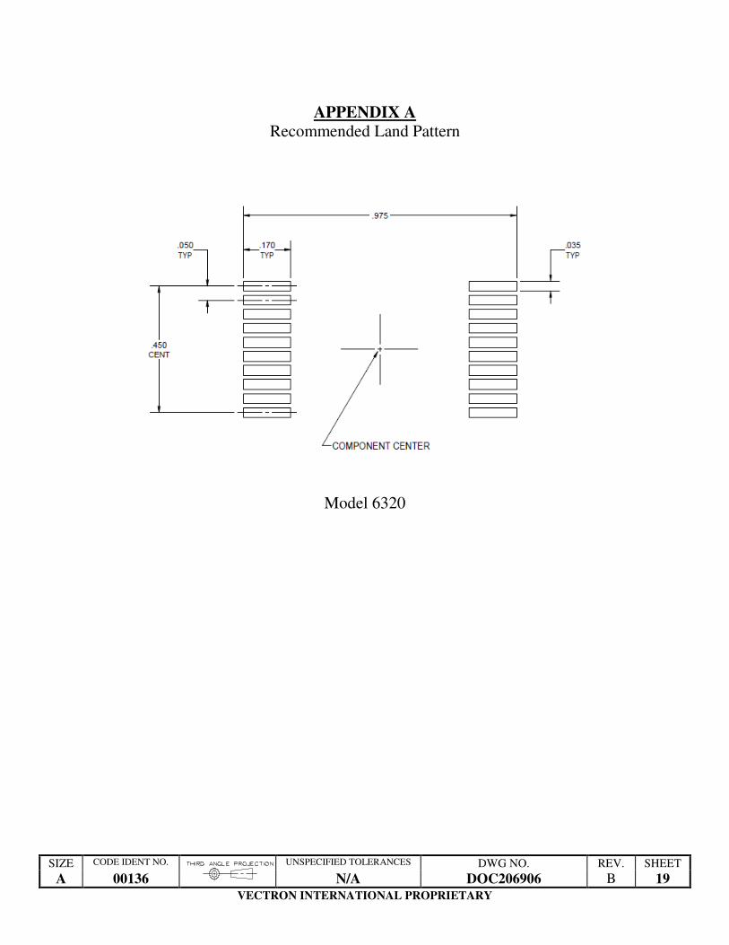
APPENDIX A
Recommended Land Pattern
Model 6320