
Wireless Components & Tailored System Solutions Application Note
32
Wireless Components & Tailored System Solutions Application Note of ATSC Tuner with TUA6034T Version 1.0 The 3 rd part of Application notes for TUA6034. Applications of IC, TUA6034 : Specially Suitable for Digital Broadcasting Standards DVB-T, DVB-C, ISDB-T, ATSC, etc.
Transcript of Wireless Components & Tailored System Solutions Application Note

Wireless Components & Tailored System Solutions
Application Note of ATSC Tuner with TUA6034T
Version 1.0The 3rd part of Application notes for TUA6034.
Applications of IC, TUA6034 :
Specially Suitable for Digital Broadcasting Standards
DVB-T, DVB-C, ISDB-T, ATSC, etc.

May.28,2003
1 Wireless products Application Engineering SMS AE DS
BF 2030W
BB 659C BB 689
1 X
4 X 4 X
TUA 6034 TUA 6034T1 X
BB 5657 X
1 X BG3130
Overview of the ATSC Tuner
Single Conversion TunerFor ATSC application
With Infineon Components of
TUA6034 Single Chip Mixer-Oscillator-PLL IC
BG3130, BF 2030W self biasing MOSFETs
BB565, BB659C and BB 689 Varactor Diodes
This small sized single conversion tuner is designed for ATSC(8-VSB) front-end in the frequency rangefrom 57 to 861MHz. The tuner is developed as a real 3 band tuner concept, designed without switchingdiodes based on the Infineon 3 band tuner IC, TUA6034 which has 3 mixer, 3 oscillators, separated SAWdriver input, PLL and balanced crystal oscillator for optimum digital front-end performance. The IC isparticularly suitable for digital tuner applications that require a high performance front-end block. The ICprovides a balanced SAW filter driver output that is designed to drive a SAW filter directly.
The tuner is optimized for IF bandwidth = 6MHz and IF center frequency = 44MHz.The frequency ranges of the tuner is as follows :
VHF I : 57 - 159 MHzVHF II: 165 - 453 MHzUHF : 459 - 861 MHz
All the passive and active components except air coils, 1 choke coil are SMD components. The PCB issingle-clad and the dimensions are 49.5 x 38.5 mm. The pin layout and the outline dimensions aredesigned according to the world standard tuner description, which is the current standard size of analogtuners in the market.
Semiconductors:

May.28,2003
2 Wireless products Application Engineering SMS AE DS
Contents
1. Introduction of the ATSC Tuner with TUA6034 .....................................3
2. PCB Layout of the Tuner ..........................................................................6
3. Measurement Results ....................................................................................7
3.1 Overall Electrical Characteristics of the Tuner ..................................7
3.2 Phase Noise ........................................................................................9
3.3 RF to IF Conversion Characteristic ..................................................19
3.4 Analog-to-Digital Interference and Internal AGC of TUA6034 ......22
4. Component Lists & Ordering Information.............................................25
Appendix 1-3. Tuner Circuit Diagram & Layout Drawings

May.28,2003
3 Wireless products Application Engineering SMS AE DS
1. Introduction of the ATSC Tuner with TUA6034
This reference tuner is developed for ATSC (Advanced Television Systems Committee) 8-VSB (Vestigial Side-band Modulation) receiver. The TV tuner is the key block to recover the original video and sound data withminimum impairments, and any of worse conversion characteristics than certain threshold level will immediatelydegrade the digital receiver performance. In fact the tuner block decides the most important receiver characteristics,sensitivity and selectivity.
Fig.1 shows a typical 8-VSB air-signal from the transmitter. Instead of the Picture/Color/Audio signal (with threepeaks) the DTV signal will show as a 6 MHz Raised Noise Floor with a spike on the lower or left side of thewaveform. DTV signal will appear almost like a spread spectrum signal with a raised noise floor, but is actually apseudo spread spectrum type of signal. The spike on the lower side of the waveform is called the ATSC Pilot whichprovides one of three timing signals within the data stream. The signal includes 19.39 Mb/s MPEG data.
Fig. 1 An example of a typical ATSC (8-VSB) signal
In a practical system, various system distortions, noise and interference will impair the signal. The overall effect ofthese impairments is to degrade the carrier-to-noise ration, C/N, and this will be C/(N+I) in the presence of strongInterference. The tuner as the first block in the digital TV receiver must guarantee a certain level of SNR, and inU.S., the FCC Advisory Committee on Advanced Television Service has recommended standard values for receivernoise figure, the loss of the receiving antenna transmission line, and antenna gain for different frequency bands.These planning factors are shown in Table.1
VHFL VHFH UHFReceiver Antenna Gain (dB) 4 6 10Line Loss (dB) 1 2 4Noise Figure (dB) 10 10 7Threshold C/N (dB) 15.2 15.2 15.2Threshold Power at Receiver (dBm) -81 -81 -84
Table 1 FCC Planning Factors and Threshold Power1
Satisfactory reception in ATSC standard is defined in terms of TOV (Threshold of Visibility) which was actuallyderived subjectively, and this C/N threshold values for trellis-coded 8-VSB is about 15.2dB as in the Table.1. Withthe current technology, the implementation loss of ATSC system is only 0.4dB, and that of DVB-T is over 2 dB.The tuner in this report is optimized to satisfy the noise figure requirement with some margins. It is verified in a lotfield-tests that noise figure of the tuner should be lower than 10dB in the whole frequency range. 1 FCC Sixth Report and Order, April 3, 1997, Appendix A.

May.28,2003
4 Wireless products Application Engineering SMS AE DS
Fig. 2 Probability of Segment Error for 8VSB-T and 16VSB2
Fig. 2 contains graphs of the segment error probabilities for both trellis-coded 8-VSB (ATSC) and 16-VSB modes.SER=2x10⁻⁴ (or BER=3x10⁻⁶) is the points where the S/N is such that one segment error per second occurs. Thethreshold of visibility (TOV) has been determined (for no video error masking in the receiver) to be at 2.5 segmenterrors/second. Fig.3 shows how 8-VSB constellation is difference between high and low SNR.
Fig. 3 8-VSB Constellations and Eye Diagram: Left = Low Noise, Right = High Noise
2 ATSC/VSB Tutorial – Receiver Technology Compiled by Wayne E. Bretl Zenith Electronics Corp.

May.28,2003
5 Wireless products Application Engineering SMS AE DS
8-VSB signal constellation diagram is series eight vertical lines that correspond to the eight transmitted amplitudelevels. In 8-VSB, the digital information is transmitted exclusively in the amplitude of the RF envelope and not inthe phase. The useful information is recovered only by sampling an In-phase synchronous detector, and no usefulinformation in a Quadrature channel.
Although the noise floor is a useful concept for estimating the coverage, in the real world interference likeharmonics, intermodulation products is often present, and affects the receiver performance badly. Part of this reportis devoted to an intermodulation test by strong analog adjacent channel, and also a solution is proposed to minimizethe intermodulation terms from the strong adjacent NTSC signals with the internal wide-band detection AGC ofTUA6034.
The tuner block diagram is shown in Fig.4
Fig. 4 Block Diagram of the ATSC Tuner with TUA6034
The ATSC tuner consists of 3 different band blocks to obtain optimal RF performance for the digital receiver.The first filter block contains a CB (Citizen Band) trap, IF trap and a simple power divider to separate the inputsignal from the antenna to each band. The following LNA blocks contain tracking filters and image traps to tune thechosen channel and to reject undesired adjacent signals. It is feasible to put a two-pole or several pole IF filters inthe tuner thanks to the separate mixer output and the IF amplifier input. In the current reference design 6MHzbandwidth 2-pole IF filter is installed. The loop filter is optimized for optimal phase noise and reference spursuppression. We can achieve much better phase noise than the required threshold of -76dBc/Hz at 20KHz offset.
As in NTSC television receivers, it is customary to employ delayed AGC in digital TV receivers. This techniquemust be carefully implemented for optimum receiver performance. In a DTV receiver, linearity of the datamodulation is critical to accurate data recovery. As long as the SNR is maintained above threshold, the SNRrequirements are less stringent than for an NTSC receiver. Accordingly it is preferred in a digital DTV to beginreduction of RF amplifier gain at a lower input signal level than in an analog receiver.

May.28,2003
6 Wireless products Application Engineering SMS AE DS
2. PCB Layout of the Tuner
A single-clad 1.5mm FR4 PCB is adopted for the tuner. The sensitive blocks in the tuner like xtal oscillator,VCO, PLL and tuning voltage lines should be well-decoupled particularly from IF output lines. Some printed partsneed to be optimized again depending on the PCB material and the tolerance of matched components.
Fig. 5 PCB Layout of the ATSC Reference Tuner with TUA6034-T

May.28,2003
7 Wireless products Application Engineering SMS AE DS
3. Measurement Results
3.1 Overall Electrical Characteristics of the Tuner
Unless otherwise specified all data were measured in conditions of supply voltage of 5 V ± 5%, AGC voltage of4.5 V ± 5%, ambient temperature of 25 º C ± 5%, fref of 62.5KHz and Icp=50uA.
Parameter Min Typ Max UnitFrequency range
VHFL 57 ~ 159 MHzVHFH 165 ~ 453 MHzUHF 459 ~ 861 MHz
IF center frequency 44IF bandwidth 6Frequency margin at low and high ends of each band 1.5
MHz
Supply voltages and currentsSupply voltage +5 V Pin 4.5 5 5.5Supply voltage VD Pin (with PLL) 30 33 35
V
Supply current +5 V Pin 85Supply current Pin VD Pin (with PLL) 1,8
mA
RF Characteristics
Input impedanceOutput impedance with IF dummy
7575
Ω
VSWR at nominal gain and during AGC 4
External AGC voltage for max gainExternal AGC voltage for min gainInternal AGC voltage (I_AGC = 9uA)
4.00.5
4.5
3.8
5.0 V
AGC range VHFLAGC range VHFHAGC range UHF
606050
dB
Tuning sensitivity VHFLTuning sensitivity VHFHTuning sensitivity UHF
153
102335
MHz/V
Power gain measured with 10:2 IF Dummy(Dummy loss = 15dB)
30 dB
Gain taper in each band 5 dB
Noise figure VHFLNoise figure VHFHNoise figure UHF
777
dB

May.28,2003
8 Wireless products Application Engineering SMS AE DS
Parameter Min Typ Max Unit
RF bandwidth (3 dB) VHFLRF bandwidth (3 dB) VHFHRF bandwidth (3 dB) UHF
101010
202020
MHz
Image rejection VHFLImage rejection VHFHImage rejection UHF
606060
dB
IF rejection VHFL VHFH, UHF
7080
dB
Input 1 dB compression Point by maximum tuner gain 75
Input IP3 (two tone) by maximum tuner gain 85
Input level producing 50 kHz of oscillator detuning(PLL open loop)
80
dBuV
Oscillator shift with supply voltage variation of ± 10 %(open loop)
± 250 kHz
Oscillator temperature drift 25...40 °C(open loop) 1 MHz
Antenna Leakage up to 1GHz 30 dBuV
Phase Noise3 10 KH offset 20 KHz offset 100 KHz offset
( fref=62.5KHz, Icp=50~250uA )
8595105
dBc/Hz
3 detailed measurement results in '3.2 Phase Noise'
May.28,2003
9 Wireless products Application Engineering SMS AE DS
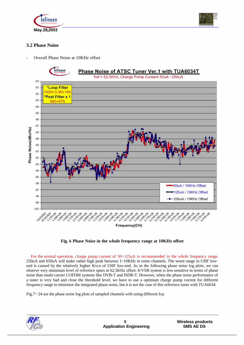
3.2 Phase Noise
- Overall Phase Noise at 10KHz offset
Fig. 6 Phase Noise in the whole frequency range at 10KHz offset
For the normal operation, charge pump current of 50~125uA is recommended in the whole frequency range.250uA and 650uA will make rather high peak between 1~10KHz in some channels. The worst range in UHF low-end is caused by the relatively higher Kvco of UHF low-end. As in the following phase noise log plots, we canobserve very minimum level of reference spurs at 62.5KHz offset. 8-VSB system is less sensitive in terms of phasenoise than multi-carrier COFDM systems like DVB-T and ISDB-T. However, when the phase noise performance ofa tuner is very bad and close the threshold level, we have to use a optimum charge pump current for differentfrequency range to minimize the integrated phase noise, but it is not the case of this reference tuner with TUA6034.
Fig.7~ 24 are the phase noise log plots of sampled channels with using different Icp.

May.28,2003
10 Wireless products Application Engineering SMS AE DS
Fig. 7 VHFL, RF=57MHz, Icp=50uA, fref=62.5KHz
Fig. 8 VHFL, RF=57MHz, Icp=125uA, fref=62.5KHz
May.28,2003
11 Wireless products Application Engineering SMS AE DS
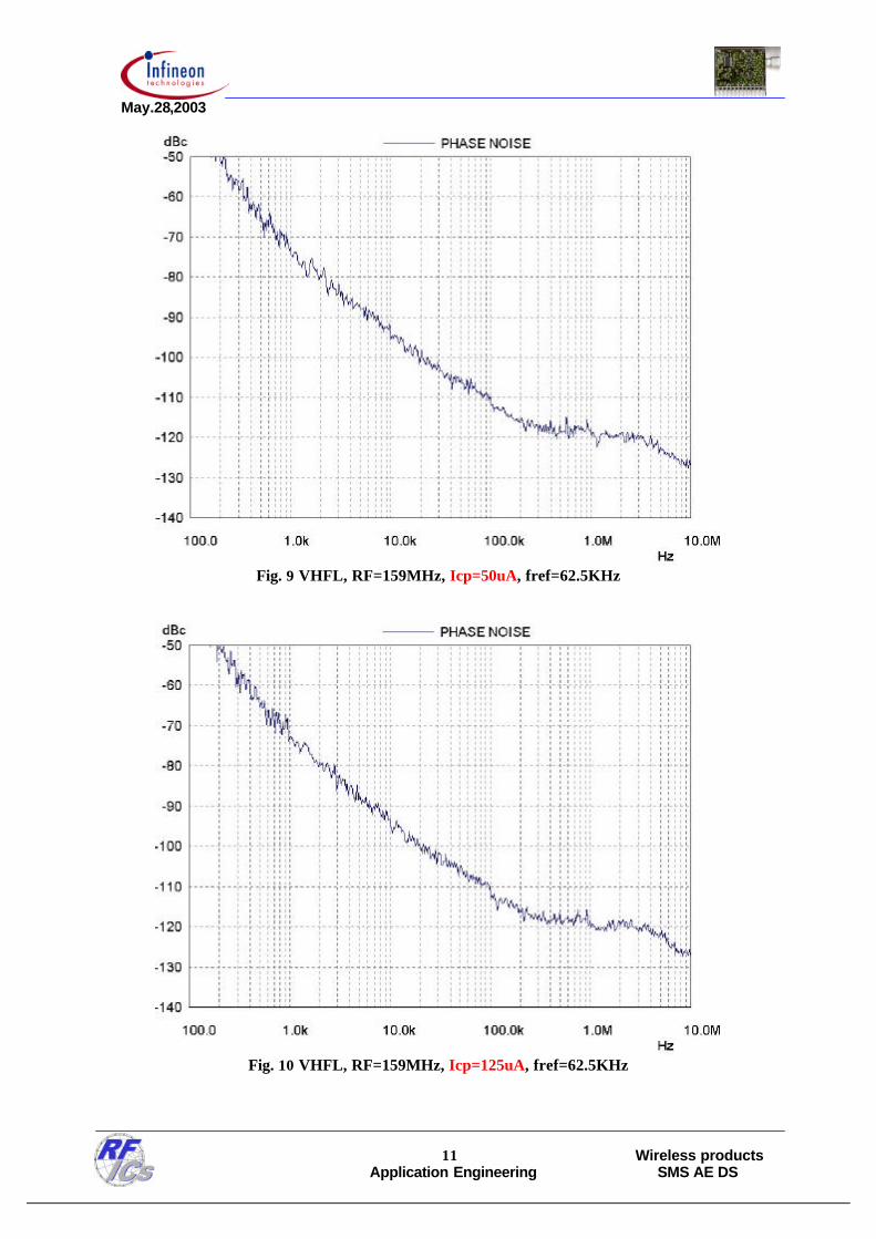
Fig. 9 VHFL, RF=159MHz, Icp=50uA, fref=62.5KHz
Fig. 10 VHFL, RF=159MHz, Icp=125uA, fref=62.5KHz

May.28,2003
12 Wireless products Application Engineering SMS AE DS
Fig. 11 VHFH, RF=165MHz, Icp=50uA, fref=62.5KHz
Fig. 12 VHFH, RF=165MHz, Icp=125uA, fref=62.5KHz

May.28,2003
13 Wireless products Application Engineering SMS AE DS
Fig. 13 VHFH, RF=303MHz, Icp=50uA, fref=62.5KHz
Fig. 14 VHFH, RF=303MHz, Icp=125uA, fref=62.5KHz

May.28,2003
14 Wireless products Application Engineering SMS AE DS
Fig. 15 VHFH, RF=453MHz, Icp=50uA, fref=62.5KHz
Fig. 16 VHFH, RF=453MHz, Icp=125uA, fref=62.5KHz

May.28,2003
15 Wireless products Application Engineering SMS AE DS
Fig. 17 UHF, RF=459MHz, Icp=50uA, fref=62.5KHz
Fig. 18 UHF, RF=459MHz, Icp=125uA, fref=62.5KHz

May.28,2003
16 Wireless products Application Engineering SMS AE DS
Fig. 19 UHF, RF=651MHz, Icp=50uA, fref=62.5KHz
Fig. 20 UHF, RF=651MHz, Icp=125uA, fref=62.5KHz

May.28,2003
17 Wireless products Application Engineering SMS AE DS
Fig. 21 UHF, RF=861MHz, Icp=50uA, fref=62.5KHz
Fig. 22 UHF, RF=861MHz, Icp=125uA, fref=62.5KHz

May.28,2003
18 Wireless products Application Engineering SMS AE DS
Fig. 23 UHF, RF=861MHz, Icp=650uA, fref=62.5KHzBetter than Icp=50uA in terms of integrated phase noise.
Fig. 24 VHFH, RF=165MHz, Icp=250uA, fref=62.5KHzRather high peak between 1~10KHz, but in-phase noise better than Icp=125uA in Fig. 12

May.28,2003
19 Wireless products Application Engineering SMS AE DS
3.3 RF to IF Conversion CharacteristicThe dummy loss of 15dB is not compensated in the whole graphs.
Mkr1 is the center frequency, and Bandwidth=6MHz from Mkr2~Mkr3
Fig. 25 VHFL, RF_Center=57MHz
Fig. 26 VHFL, RF_Center=159MHz

May.28,2003
20 Wireless products Application Engineering SMS AE DS
Fig. 27 VHFH, RF_Center=303MHz
Fig. 28 UHF, RF_Center=459MHz

May.28,2003
21 Wireless products Application Engineering SMS AE DS
Fig. 29 UHF, RF_Center=651MHz
Fig. 30 UHF, RF_Center=861MHz

May.28,2003
22 Wireless products Application Engineering SMS AE DS
3.4 Analog-to-Digital Interference and Internal AGC of TUA6034
This part of the report contains an example of how a strong adjacent analog signal affects a desired digital signalby generating an IM3 terms inside the channel bandwidth.
- f1, Desired Signal = 171MHz, -56dBm(50ohm), f_osc = 215MHz, f_IF = 44MHz.- f2, Analog NTSC Picture Carrier = 175.25MHz, -21dBm(50ohm)- f3, Analog NTSC Sound Carrier = 179.75MHz, -27dBm(50ohm)- Beat, IM3 term inside the bandwidth = 215MHz - ( 2 x 175.25MHz - 179.25MHz ) = 44.25MHz.
Fig.31 shows the tuner input signals for the test.
Fig. 31 Tuner Input Signals for Intermodulation test;M1=Desired Digital Carrier, M2=Analog Picture Carrier, M3=Analog Sound Carrier
Fig.32 shows the output signals from the tuner via the input signals in Fig.31 when the tuner gain is full, no gainreduction. IM3 term at 44.25MHz is higher that the desired 44MHz. In the real situation this IM3 product willdegrade the receiver performance seriously. This intermodulation product is generated by the mixer in the tunerbecause it has normally the worst linear characteristic.

May.28,2003
23 Wireless products Application Engineering SMS AE DS
Fig. 32 Tuner Output Signals by Input Signals in Fig.31;M1=Desired IF of 44MHz , M2=Undesired IM3 Product of 44.25MHz
In this kind of situation, internal wide-band detection AGC function of TUA6034 really helps not overdrive themixer and immediately suppress such IM3 product caused by adjacent channels. Because of the low SNRrequirement of 15.2dB, we still can maintain the SNR required by the demodulator although the desired signal isalso lowered. 106 ~112 dBuV internal AGC take-over point were taken to test this internal AGC functioning.
Table 2 contains the results by each internal AGC take-over point. V_ AGC voltages were measured when the internalAGC was working loaded with the input signals in Fig.31. NF (Noise Figure) was measured after the test withsupplying the measured AGC voltage and the SNR at the tuner output were calculated using the equation below:
F = (S/N) input / (S/N) output , NF [dB] = 10logFNF dB = S input -10log(kTB) - (S/N) output à (S/N) output dB = S input - 10log(kTB) - NF
AGC Take-Over Point(dBuV)
V_AGC (Volts) Delta = 44MHz - Beat Level(dB)
NF (dB) SNR (dB)
106 1.65 314 23 27.2109 1.68 275 20 30.2112 1.72 25 18 32.2
Table 2. Interal AGC Test to Suppress Intermodulation
If we use the wide-band detection AGC function of TUA6034 for digital receivers, we can protect the first mixerfrom overdriving and still maintain the required SNR for demodulation process even considering the followingstages after the tuner like SAW filters and the SAW drivers. Fig.33 and Fig.34 show the result by using the internal
4 Fig.335 Fig.34

May.28,2003
24 Wireless products Application Engineering SMS AE DS
AGC function. However, this wide-band detection internal AGC cannot be adopted for analog receivers whichrequire more than 55dB SNR for a quality picture.
Fig. 33 Tuner Output Signals, Internal AGC take-over point=106dBuV
Fig. 34 Tuner Output Signals, Internal AGC take-over point=109dBuV

May.28,2003
25 Wireless products Application Engineering SMS AE DS
4. Component List & Ordering Information (units : Farad, Ohm)Part Value Size Tolerance Material Part Value Size Tolerance MaterialC1 330p O6O3 10% NPO C51 27p O6O3 5% N750C2 150p O6O3 10% NPO C52 1.5p O6O3 5% N750C3 9.1p O6O3 5% NPO C53 1.2p O6O3 5% N750C4 1n O6O3 10% X7R C54 82p O6O3 5% N750C5 2.4p O6O3 5% NPO C55 1.2p O6O3 5% N750C6 OPEN O6O3 5% NPO C56 1.2p O6O3 5% N750C7 4.7n O6O3 10% X7R C57 1.2p O6O3 5% N750C8 0.5p O6O3 5% NPO C58 1.2p O6O3 5% N750C9 1n O6O3 10% X7R C59 16p O6O3 5% N750
C10 4.7n O6O3 10% X7R C60 4.7n O6O3 10% X7RC11 10n O8O5 10% X7R C61 4.7n O6O3 10% X7RC12 10n O6O3 10% X7R C62 4.7n O6O3 10% X7RC13 91p O6O3 5% NPO C63 4.7n O6O3 10% X7RC14 4.7n O6O3 10% X7R C64 4.7n O6O3 10% X7RC15 470p O6O3 10% X7R C65 3.3n O6O3 10% X7RC16 4.7n O6O3 10% X7R C66 18p O6O3 5% NPOC17 C67 OPENC18 4.7n O6O3 10% X7R C68 100nF Foil CapacitorC19 4.7n O6O3 10% X7R C69 100n O8O5 10% X7RC20 4.7n O6O3 10% X7R C70 160n O8O5 10% X7RC21 4.7n O6O3 10% X7R C71 4.7n O6O3 10% X7RC22 4.7n O6O3 10% X7R C72 4.7n O6O3 10% X7RC23 4.7n O6O3 10% X7R C75 56p O6O3 5% NPOC24 47n O8O5 10% X7R C76,C77 18p O6O3 5% NPOC25 4.7n O6O3 10% X7R R1 33K O6O3 5%C26 4.7n O8O5 10% X7R R2 33K O6O3 5%C27 1.2p O6O3 5% NPO R3 33K O6O3 5%C28 100p O6O3 5% NPO R4 22 O6O3 5%C29 13p O6O3 5% NPO R5 33K O6O3 5%C30 13p O6O3 5% NPO R6 33K O6O3 5%C31 27p O6O3 10% X7R R7 10K O6O3 5%C32 27p O6O3 10% X7R R8 10K O6O3 5%C33 1.8p O6O3 5% NPO R9C34 120p O6O3 5% NPO R10 33K O6O3 5%C35 120p O6O3 5% NPO R11 5.6 O8O5 5%C36 470p O6O3 10% X7R R12 22 O6O3 5%C37 470p O6O3 10% X7R R13 22 O6O3 5%C38 120p O6O3 5% NPO R14 33k O6O3 5%C39 470p O6O3 10% X7R R16 100K O6O3 5%C40 47p O6O3 5% NPO R18 150K O6O3 5%C41 OPEN R19 150K O6O3 5%C42 4.7n O6O3 10% X7R R20 33K O6O3 5%C43 4.7n O6O3 10% X7R R21 33K O6O3 5%C44 4.7n O8O5 10% X7R R22 33K O6O3 5%C45 100p O8O5 5% NPO R23 33K O6O3 5%C46 100p O8O5 5% NPO R24 OPEN O6O3C47 4.7n O8O5 10% X7R R25 2.7 O6O3 5%C48 560p O6O3 10% X7R R26 0 O6O3C49 2.7p O6O3 5% N750 R27 OPEN O6O3 5%C50 2.2p O6O3 5% N750 R28 33K O6O3 5%

May.28,2003
26 Wireless products Application Engineering SMS AE DS
Part Value Size Tolerance Part Turns D.of Wire D. of Coil Direction Pre-form.R29 330 O6O3 5% L1 12 0.4 2.2 CWR30 330 O6O3 5% L2 12 0.4 2.4 CWR31 12 O6O3 5% L3 9 0.3 2 CWR32 2.2k O8O5 5% L4 6 0.3 1.6 CCWR33 8.2 O6O3 5% L5 3 0.4 2.2 CWR34 2.7k O6O3 5% L6 PrintedR35 5.6 O6O3 5% L7 9 0.3 2 CCWR36 1.8k O6O3 5% L8 5 0.4 1.8 CWR37 1.8k O6O3 5% L9 13 0.3 3 CWR38 OPEN L10 18 0.3 3.2 CWR39 18K O6O3 5% L11 8 0.3 1.8 CWR40 560 O8O5 5% L12 15 0.3 1.9 CWR42 1.2K O6O3 5% L13 Choke Coil=3.9uHJ1 0 O6O3 L14 5 0.3 1.7 CCWJ2 0 O8O5 L15 3 0.4 1.9 CCW 0.5mmJ3 0 O8O5 L16 2 0.5 1.6 CW 0.5mmJ4 0 O8O5 L17 PrintedJ5 0 O6O3 L18 2 0.5 1.6 CCWJ6 0 O6O3 L19 4 0.4 1.7 CWJ7 0 O8O5 L20 4 0.4 1.7 CWJ8 0 O8O5 L21 4 0.4 2 CW 0.5mmJ9 0 O8O5 L22 4 0.4 1.6 CW 0.5mmJ10 0 O8O5 L23 PrintedR15 10k O6O3 5% L24 4 0.4 1.6 CCW 0.5mmR17 15 O6O3 5% L25 8 0.3 2 CCWR41 15 O6O3 5% L26 8 0.3 2 CWJ12 0 O6O3 L27 14 0.3 2 CW
L28 14 0.3 2 CWL29 8 0.3 1.6 CCW
L30,L36 220nH SMD 0805L31 14 0.3 2 CWL32 4 0.4 1.9 CW 0.5mmL33 2 0.4 1.9 CW 0.5mmL34 12 0.3 2.3 CWL35 12 0.3 2.3 CW
Note1) All the coils are full-turn types. The Unit of the Diameter of Coil & Wire is 'mm'.Full-Turn, CCW
Note2) J1 & C70 are only for internal Tuner AGC.Note3) Pre-form. value is the distance between each turn of the coils. The pre-formation of coilscxcxcx should be done before alignment by a coil manufacturer or by line workers.

May.28,2003
27 Wireless products Application Engineering SMS AE DS
Part Semiconductor Package Company Ordering CodeIC1 TUA6034-T TSSOP-38 Infineon Technologies AG Q67034-H0006TR1 BF2030W SOT343 Infineon Technologies AG Q62702-F1774 TR2 BG3130 SOT363 Infineon Technologies AG Q62702-A3850VD1 BB565 SCD80 SC79 Infineon Technologies AG Q62702-B873VD2 BB659C SCD-80 SC79 Infineon Technologies AG Q62702-B884VD3 BB565 SCD-80 SC79 Infineon Technologies AG Q62702-B873VD4 BB565 SCD-80 SC79 Infineon Technologies AG Q62702-B873VD5 BB689 SOD-80 SC79 Infineon Technologies AG Q62702-B890VD6 BB565 SCD-80 SC79 Infineon Technologies AG Q62702-B873VD7 BB565 SCD-80 SC79 Infineon Technologies AG Q62702-B873VD8 BB659C SCD-80 SC79 Infineon Technologies AG Q62702-B884VD9 BB659C SCD-80 SC79 Infineon Technologies AG Q62702-B884VD10 BB565 SCD-80 SC79 Infineon Technologies AG Q62702-B873VD11 BB689 SOD-80 SC79 Infineon Technologies AG Q62702-B890VD12 BB689 SCD-80 SC79 Infineon Technologies AG Q62702-B890VD13 BB689 SOD-80 SC79 Infineon Technologies AG Q62702-B890VD14 BB659C SOD-80 SC79 Infineon Technologies AG Q62702-B884VD15 BB565 SCD-80 SC79 Infineon Technologies AG Q62702-B873
Q1 4MHzPCB FR4 / 1.5mmJack 75 Ω IEC or F- type
Pin-Head Standard Pin
Ordering & Contact Information
Please visit our website at
http://www.infineon.com

May.28,2003
28 Wireless products Application Engineering SMS AE DS
Edition February.2003Published by Infineon Technologies AG, SMS M AE DSKastenbauerstr 2,81677 München© Infineon Technologies AG . 02.03.All Rights Reserved.
Attention please!As far as patents or other rights of third parties are concerned, liability is only assumed for components,not for applications, processes and circuits implemented within components or assemblies.The information describes the type of component and shall not be considered as assured characteristics.Terms of delivery and rights to change design reserved.Due to technical requirements components may contain dangerous substances. For information on thetypes in question please contact your nearest Infineon Technologies Office.Infineon Technologies AG is an approved CECC manufacturer.
PackingPlease use the recycling operators known to you. We can also help you – get in touch with your nearestsales office. By agreement we will take packing material back, if it is sorted. You must bear the costs oftransport.For packing material that is returned to us unsorted or which we are not obliged to accept, we shall haveto invoice you for any costs incurred.Components used in life-support devices or systems must be expressly authorized for suchpurpose!Critical components 1 of the Infineon Technologies AG, may only be used in life-support devices orsystems 2 with the express written approval of the Infineon Technologies AG.
1 A critical component is a component used in a life-support device or system whose failure canreasonably be expected to cause the failure of that life-support device or system, or to affect its safety oreffectiveness of that device or system.
2 Life support devices or systems are intended (a) to be implanted in the human body, or (b) to supportand/or maintain and sustain human life. If they fail, it is reasonable to assume that the health of the usermay be endangered.


![Components for Wireless Communication Mechanical/Electrical … · 2017-12-14 · Wireless Communication Components [Nguyen et al., 1998] Texas Christian University Department of](https://static.fdocuments.us/doc/165x107/5f508fa37a2b4f622060fadd/components-for-wireless-communication-mechanicalelectrical-2017-12-14-wireless.jpg)


![IEEE MICROWAVE AND WIRELESS COMPONENTS ...arXiv:1805.03783v1 [eess.SP] 10 May 2018 IEEE MICROWAVE AND WIRELESS COMPONENTS LETTERS 1 Continuously Tunable Dual-mode Bandstop Filter Amir](https://static.fdocuments.us/doc/165x107/5e7375897f5291376d3d7de2/ieee-microwave-and-wireless-components-arxiv180503783v1-eesssp-10-may-2018.jpg)