Wireless Communication with Nanoplasmonic Data Carriers ... NanoLetters.pdf · 39 convert channel...
6
1 Wireless Communication with Nanoplasmonic Data Carriers: 2 Macroscale Propagation of Nanophotonic Plasmon Polaritons 3 Probed by Near-Field Nanoimaging 4 Moshik Cohen,* ,†,§ Yossi Abulafia, § Dmitry Lev, ∥ Aaron Lewis, ∥ Reuven Shavit, ‡ and Zeev Zalevsky †,§ 5 † Faculty of Engineering, Bar-Ilan University, Ramat-Gan 52900, Israel 6 ‡ Department of Electrical and Computer Engineering, Ben-Gurion University of the Negev, Beer-Sheva 84105, Israel 7 § Bar-Ilan Institute for Nanotechnology & Advanced Materials, Ramat-Gan 52900, Israel 8 ∥ Department of Applied Physics, Selim and Rachel Benin School of Engineering and Computer Science, The Hebrew University, 9 Givat Ram, Jerusalem 9190401, Israel 10 ABSTRACT: The ability to control the energy flow of light at the nanoscale is 11 fundamental to modern communication and big-data technologies, as well as quantum 12 information processing schemes. However, because photons are diffraction-limited, efforts 13 of confining them to dimensions of integrated electronics have so far proven elusive. A 14 promising way to facilitate nanoscale manipulation of light is through plasmon 15 polaritonscoupled excitations of photons and charge carriers. These tightly confined 16 hybrid waves can facilitate compression of optical functionalities to the nanoscale but suffer 17 from huge propagation losses that limit their use to mostly subwavelength scale 18 applications. With only weak evidence of macroscale plasmon polaritons, propagation has 19 recently been reported theoretically and indirectly, no experiments so far have directly 20 resolved long-range propagating optical plasmon polaritons in real space. Here, we launch 21 and detect nanoscale optical signals, for record distances in a wireless link based on novel 22 plasmonic nanotransceivers. We use a combination of scanning probe microscopies to 23 provide high resolution real space images of the optical near fields and investigate the long- 24 range propagation of nanoscales optical signals. We design our nanotransceivers based on a high-performance nanoantenna, 25 Plantenna, hybridized with channel plasmon waveguides with a cross-section of 20 nm × 20 nm, and observe propagation for 26 distances up to 1000 times greater than the plasmon wavelength. We experimentally show that our approach hugely outperforms 27 both waveguide and wireless nanophotonic links. This successful alliance between Plantenna and channel plasmon waveguides 28 paves the way for new generations of optical interconnects and expedites long-range interaction between quantum emitters and 29 photomolecular devices. 30 KEYWORDS: Plasmonics, nanoantennas, channel waveguides, wireless, nanoimaging 31 T he proposed scheme is designed to enable macroscale 32 communication between nanoscale devices utilizing 33 surface plasmon polaritons (SPPs). Hence, we use channel 34 waveguides that confine SPPs to their channel dimensions, 35 which can be as small as several nanometers. 1−8 However, as 36 dimensions decrease, SPPs exhibit increased losses that limit 37 their propagation in waveguides to distances of only few 38 micrometers. To address this fundamental limitation, we 39 convert channel SPPs to optical surface waves that propagate 40 for significantly larger distances on dielectric substrates. A high- 41 efficiency nanoreceiver, designed to convert surface waves to f1 42 channel SPPs, is placed the remote edge of the system. Figure f1 43 1a illustrates the proposed communication nanosystem, which 44 (a) converts light to nanoscale SPPs, (b) propagates SPPs in 45 channel waveguide, (c) converts these SPPs to surface waves 46 and propagatea them for long distance, and (d) excites SPPs 47 from the surface waves at remote locations. As shown in the 48 right-hand side of Figure 1a, laser light illuminates the 49 Plantenna to launch SPPs at the waveguide. Second, Plantenna, 50 located at the other edge of the waveguide, converts these SPPs 51 to surface waves that propagate on the substrate. The surface 52 waves are reconverted to SPPs at a remote, Plantenna based 53 nanoreceiver. We use waveguides with a propagation loss of 54 e −αl , where the absorption constant α = (18 μm) −1 for a 55 channel width of 20 nm at a red wavelength of λ = 633 nm and 56 l is the propagation length. 57 In contrast, absorption for wireless links occur only at the 58 antennas and are much lower than for a waveguide. For 59 conventional (e.g., dipole, bowtie) nanoantennas, the prop- 60 agation loss for wireless links behaves like (D/l) 2 , where D is 61 the directivity. 9 Here, we show that Plantenna based wireless 62 links hugely outperform both waveguide and conventional 63 nanoantenna based alternatives. Figure 1b presents a 3D model 64 of the nanotransceiver, with zoom in to the Plantenna region Received: January 19, 2017 Revised: April 25, 2017 Published: May 3, 2017 Letter pubs.acs.org/NanoLett © XXXX American Chemical Society A DOI: 10.1021/acs.nanolett.7b00266 Nano Lett. XXXX, XXX, XXX−XXX amc00 | ACSJCA | JCA10.0.1465/W Unicode | research.3f (R3.6.i12 HF02:4458 | 2.0 alpha 39) 2016/10/28 09:46:00 | PROD-JCAVA | rq_8555253 | 5/04/2017 14:18:36 | 6 | JCA-DEFAULT
Transcript of Wireless Communication with Nanoplasmonic Data Carriers ... NanoLetters.pdf · 39 convert channel...

1 Wireless Communication with Nanoplasmonic Data Carriers:2 Macroscale Propagation of Nanophotonic Plasmon Polaritons3 Probed by Near-Field Nanoimaging4 Moshik Cohen,*,†,§ Yossi Abulafia,§ Dmitry Lev,∥ Aaron Lewis,∥ Reuven Shavit,‡ and Zeev Zalevsky†,§
5†Faculty of Engineering, Bar-Ilan University, Ramat-Gan 52900, Israel
6‡Department of Electrical and Computer Engineering, Ben-Gurion University of the Negev, Beer-Sheva 84105, Israel
7§Bar-Ilan Institute for Nanotechnology & Advanced Materials, Ramat-Gan 52900, Israel
8∥Department of Applied Physics, Selim and Rachel Benin School of Engineering and Computer Science, The Hebrew University,
9 Givat Ram, Jerusalem 9190401, Israel
10 ABSTRACT: The ability to control the energy flow of light at the nanoscale is11 fundamental to modern communication and big-data technologies, as well as quantum12 information processing schemes. However, because photons are diffraction-limited, efforts13 of confining them to dimensions of integrated electronics have so far proven elusive. A14 promising way to facilitate nanoscale manipulation of light is through plasmon15 polaritonscoupled excitations of photons and charge carriers. These tightly confined16 hybrid waves can facilitate compression of optical functionalities to the nanoscale but suffer17 from huge propagation losses that limit their use to mostly subwavelength scale18 applications. With only weak evidence of macroscale plasmon polaritons, propagation has19 recently been reported theoretically and indirectly, no experiments so far have directly20 resolved long-range propagating optical plasmon polaritons in real space. Here, we launch21 and detect nanoscale optical signals, for record distances in a wireless link based on novel22 plasmonic nanotransceivers. We use a combination of scanning probe microscopies to23 provide high resolution real space images of the optical near fields and investigate the long-24 range propagation of nanoscales optical signals. We design our nanotransceivers based on a high-performance nanoantenna,25 Plantenna, hybridized with channel plasmon waveguides with a cross-section of 20 nm × 20 nm, and observe propagation for26 distances up to 1000 times greater than the plasmon wavelength. We experimentally show that our approach hugely outperforms27 both waveguide and wireless nanophotonic links. This successful alliance between Plantenna and channel plasmon waveguides28 paves the way for new generations of optical interconnects and expedites long-range interaction between quantum emitters and29 photomolecular devices.
30 KEYWORDS: Plasmonics, nanoantennas, channel waveguides, wireless, nanoimaging
31 The proposed scheme is designed to enable macroscale32 communication between nanoscale devices utilizing33 surface plasmon polaritons (SPPs). Hence, we use channel34 waveguides that confine SPPs to their channel dimensions,35 which can be as small as several nanometers.1−8 However, as36 dimensions decrease, SPPs exhibit increased losses that limit37 their propagation in waveguides to distances of only few38 micrometers. To address this fundamental limitation, we39 convert channel SPPs to optical surface waves that propagate40 for significantly larger distances on dielectric substrates. A high-41 efficiency nanoreceiver, designed to convert surface waves to
f1 42 channel SPPs, is placed the remote edge of the system. Figuref1 43 1a illustrates the proposed communication nanosystem, which
44 (a) converts light to nanoscale SPPs, (b) propagates SPPs in45 channel waveguide, (c) converts these SPPs to surface waves46 and propagatea them for long distance, and (d) excites SPPs47 from the surface waves at remote locations. As shown in the48 right-hand side of Figure 1a, laser light illuminates the49 Plantenna to launch SPPs at the waveguide. Second, Plantenna,
50located at the other edge of the waveguide, converts these SPPs51to surface waves that propagate on the substrate. The surface52waves are reconverted to SPPs at a remote, Plantenna based53nanoreceiver. We use waveguides with a propagation loss of54e−αl, where the absorption constant α = (18 μm)−1 for a55channel width of 20 nm at a red wavelength of λ = 633 nm and56l is the propagation length.57In contrast, absorption for wireless links occur only at the58antennas and are much lower than for a waveguide. For59conventional (e.g., dipole, bowtie) nanoantennas, the prop-60agation loss for wireless links behaves like (D/l)2, where D is61the directivity.9 Here, we show that Plantenna based wireless62links hugely outperform both waveguide and conventional63nanoantenna based alternatives. Figure 1b presents a 3D model64of the nanotransceiver, with zoom in to the Plantenna region
Received: January 19, 2017Revised: April 25, 2017Published: May 3, 2017
Letter
pubs.acs.org/NanoLett
© XXXX American Chemical Society A DOI: 10.1021/acs.nanolett.7b00266Nano Lett. XXXX, XXX, XXX−XXX
amc00 | ACSJCA | JCA10.0.1465/W Unicode | research.3f (R3.6.i12 HF02:4458 | 2.0 alpha 39) 2016/10/28 09:46:00 | PROD-JCAVA | rq_8555253 | 5/04/2017 14:18:36 | 6 | JCA-DEFAULT
65 shown in the inset. The physical principle behind the Plantenna66 invention is the enormous field enhancement and confinement67 exhibited by resonant, optically illuminated adjacent metallic68 nanoparticles. These properties, mainly originated from69 coherent capacitive coupling between the particles, are70 significantly better than those of isolated nanoparticles. The71 Plantenna comprised of two metallic nanorods of length LArm,72 separated by a nanoscopic gap (s = 10−35 nm), in a dipole73 arrangement. An additional nanorod, termed director, is placed74 at much closer proximity of only 7 nm (g ∼ 7 nm) to the75 dipole. A detailed analysis on the Plantenna physics, which also76 includes optimization for high efficiency excitation of channel77 SPPs, was recently reported.5 Figure 1c shows the material78 stack up used in this work, comprised of 20 nm Au layer79 deposited on a Si on insulator (SOI) wafer (500 μm Si, 2 μm80 SiO2), for potential CMOS computability.81 For nanofabrication, we use electron beam lithography82 (EBL), ion beam sputtering (Au, 20 nm), and liftoff. After83 liftoff, the resist is completely removed, allowing contact mode84 near-field optical characterization. We fabricated devices85 comprised of standalone nanotransceivers and complete
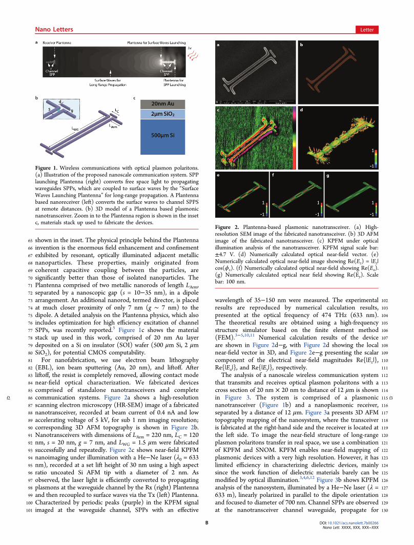
f2 86 communication systems. Figure 2a shows a high-resolution87 scanning electron microscopy (HR-SEM) image of a fabricated88 nanotransceiver, recorded at beam current of 0.4 nA and low89 accelerating voltage of 5 kV, for sub 1 nm imaging resolution;90 corresponding 3D AFM topography is shown in Figure 2b.91 Nanotransceivers with dimensions of LArm = 220 nm, LC = 12092 nm, s = 20 nm, g = 7 nm, and LWG = 1.5 μm were fabricated93 successfully and repeatedly. Figure 2c shows near-field KPFM94 nanoimaging under illumination with a He−Ne laser (λ0 = 63395 nm), recorded at a set lift height of 30 nm using a high aspect96 ratio uncoated Si AFM tip with a diameter of 2 nm. As97 observed, the laser light is efficiently converted to propagating98 plasmons at the waveguide channel by the Rx (right) Plantenna99 and then recoupled to surface waves via the Tx (left) Plantenna.100 Characterized by periodic peaks (purple) in the KPFM signal101 imaged at the waveguide channel, SPPs with an effective
102wavelength of 35−150 nm were measured. The experimental103results are reproduced by numerical calculation results,104presented at the optical frequency of 474 THz (633 nm).105The theoretical results are obtained using a high-frequency106structure simulator based on the finite element method107(FEM).3−5,10,11 Numerical calculation results of the device108are shown in Figure 2d−g, with Figure 2d showing the local109near-field vector in 3D, and Figure 2e−g presenting the scalar110component of the electrical near-field magnitudes Re{|Ez|},111Re{|Ex|}, and Re{|Ey|}, respectively.112The analysis of a nanoscale wireless communication system113that transmits and receives optical plasmon polaritons with a114cross section of 20 nm × 20 nm to distance of 12 μm is shown115 f3in Figure 3. The system is comprised of a plasmonic116nanotransceiver (Figure 1b) and a nanoplasmonic receiver,117separated by a distance of 12 μm. Figure 3a presents 3D AFM118topography mapping of the nanosystem, where the transceiver119is fabricated at the right-hand side and the receiver is located at120the left side. To image the near-field structure of long-range121plasmon polaritons transfer in real space, we use a combination122of KPFM and SNOM. KPFM enables near-field mapping of123plasmonic devices with a very high resolution. However, it has124limited efficiency in characterizing dielectric devices, mainly125since the work function of dielectric materials barely can be126modified by optical illumination.3,4,6,12 Figure 3b shows KPFM127analysis of the nanosystem, illuminated by a He−Ne laser (λ =128633 m), linearly polarized in parallel to the dipole orientation129and focused to diameter of 700 nm. Channel SPPs are observed130at the nanotransceiver channel waveguide, propagate for
Figure 1. Wireless communications with optical plasmon polaritons.(a) Illustration of the proposed nanoscale communication system. SPPlaunching Plantenna (right) converts free space light to propagatingwaveguides SPPs, which are coupled to surface waves by the “SurfaceWaves Launching Plantenna” for long-range propagation. A Plantennabased nanoreceiver (left) converts the surface waves to channel SPPSat remote distances. (b) 3D model of a Plantenna based plasmonicnanotransceiver. Zoom in to the Plantenna region is shown in the insetc, materials stack up used to fabricate the devices.
Figure 2. Plantenna-based plasmonic nanotransceiver. (a) High-resolution SEM image of the fabricated nanotransceiver. (b) 3D AFMimage of the fabricated nanotransceiver. (c) KPFM under opticalillumination analysis of the nanotransceiver. KPFM signal scale bar:±4.7 V. (d) Numerically calculated optical near-field vector. (e)Numerically calculated optical near-field image showing Re(Ez) = |Ez|cos(ϕz). (f) Numerically calculated optical near-field showing Re(Ex).(g) Numerically calculated optical near field showing Re(Ey). Scalebar: 100 nm.
Nano Letters Letter
DOI: 10.1021/acs.nanolett.7b00266Nano Lett. XXXX, XXX, XXX−XXX
B

131distance of LWG = 1 μm, followed by strong “hot spot” at the Tx132Plantenna that converts them to surface waves. A zoom in to133the channel region is presented in the inset, clearly showing the134periodic structure of the excited SPPs. Remarkably, pronounced135SPP excitation is observed at the distanced receiver, which is136not illuminated by the laser. Highlighted in the left inset, the137channel SPPs at the receiver waveguide are excited by efficient138coupling of surface waves to SPP by the receiver Plantenna.139The surface waves on the SiO2 surface are imaged in the near140field via SNOM, as shown in Figure 3c. Naturally, SNOM141provides lower resolution images compared to KPFM;3
142however, its direct optical imaging mechanism enables mapping143of the surface photons that propagate on the dielectric medium,144unlike KPFM. Note that the SNOM image exhibits high145intensity at the physical locations of the transceiver and146receiver, originated by plasmon excitation. Hence, we state that147the combination of KPFM and SNOM provides a comple-148mentary, complete real-space nanoimaging approach for the149characterization of nanoscale wireless communication systems,150which facilitates high-resolution nanoimaging of both plasmons151and optical surface waves. Numerical calculation results of the152nanosystem, presenting the electric near-field magnitude |E|, are153shown in Figure 3d. Both channel SPPs as well as the surface154waves in the dielectric substrate are clearly captured, providing155additional confirmation to our approach.156To unambiguously demonstrate the excellent efficiency of157our Plantenna based nanosystem, we compare its performances158to direct channel waveguiding link6−8,13 and to wireless link159based on dipole nanoantennas.14−17 For the wireless link160 f4configurations (Figure 4a−d) the distance between the161transceiver and receiver is 10 μm, and for the direct link162(e.g., Figure 4e−f) the waveguide length is 3 μm, limited by163fabrication constraints. Figure 4a shows AFM image of our164proposed Plantenna based nanosystem, as the corresponding165KPFM mapping is shown in Figure 4b with a voltage scale bar166of ±4.7 V. Pronounced plasmon excitation is probed at the167receiver, evidenced by the modal structure of the field inside
Figure 3. Characterization of the proposed wireless link, demonstrat-ing efficient long-range propagation of tightly confined opticalplasmon polaritons. (a) 3D AFM image of the fabricated wirelesslink system. (b) KPFM under optical illumination analysis of thewireless link system, showing SPPs at the transmission (right) andreception (left) sides; insetzoom in to the respective waveguidechannel. KPFM signal scale bar: ±4.7 V. (c) SNOM analysis of thewireless link system, showing SPPs at the transmission (right) andreception (left) sides, as well as the coupling to surface waves thatenable the long-range propagation. (d) Numerically calculated near-field image, showing the complete optical wireless transfer link. Scalebar: 750 nm.
Figure 4. Comparison between nanophotonic links. (a) 3D AFM image of the Plantenna-based wireless link system. (b) KPFM under opticalillumination analysis of the Plantenna-based wireless link system; KPFM signal scale bar: ±4.7 V. (c) 3D AFM image of the dipole nanoantenna-based wireless link system. (d) KPFM under optical illumination analysis of the dipole nanoantenna-based wireless link system; KPFM signal scalebar: ±0.5 V. (e) 3D AFM image of channel SPP waveguide with an identical cross section to the waveguides in a−d and 3 μm length. (f) KPFMunder optical illumination analysis of the channel SPP waveguide link; KPFM signal scale bar: ±4.7 V; inset (b, d, f): zoom in to the respectivewaveguide channel. Scale bar: 1 μm.
Nano Letters Letter
DOI: 10.1021/acs.nanolett.7b00266Nano Lett. XXXX, XXX, XXX−XXX
C
168 the channel which is highlighted in the inset. Figure 4c shows169 the AFM topography of a wireless link based on dipole170 nanoantennas, which was recently proposed as an approach for171 plasmonic energy transfer;18 the corresponding KPFM image is172 presented in Figure 4d with a voltage scale bar of ±0.5 V.173 We observe plasmon excitation at the transceiver; however,174 significantly less noticeable intensity is measured at the receiver175 waveguide (see inset) compared with the Plantenna based176 architecture. Figure 4e shows a 3D AFM image of a Plantenna177 integrated with a similar waveguide of 3 μm length,178 implementing a direct nanoplasmonic link. Unlike the wireless179 links, the waveguide exhibits much higher propagation loss180 since it directly propagates tightly confined plasmons that181 interacts with the metals in their entire guided route.18 A182 KPFM map of the direct link is shown in Figure 4f (scale bar183 ±4.7 V), where the zoom in to the different channel regions is184 presented in the insets. As seen in the right inset, channel SPPs185 are excited by the Plantenna and propagate through the186 waveguide. However, the huge propagation loss makes the187 waveguide SPPs decay significantly and being practically188 unobservable after propagating for only 2.5 μm, as seen in189 the left inset of Figure 4f. This reconfirms the critical, huge190 losses exhibited in gap plasmon waveguides with nanoscale
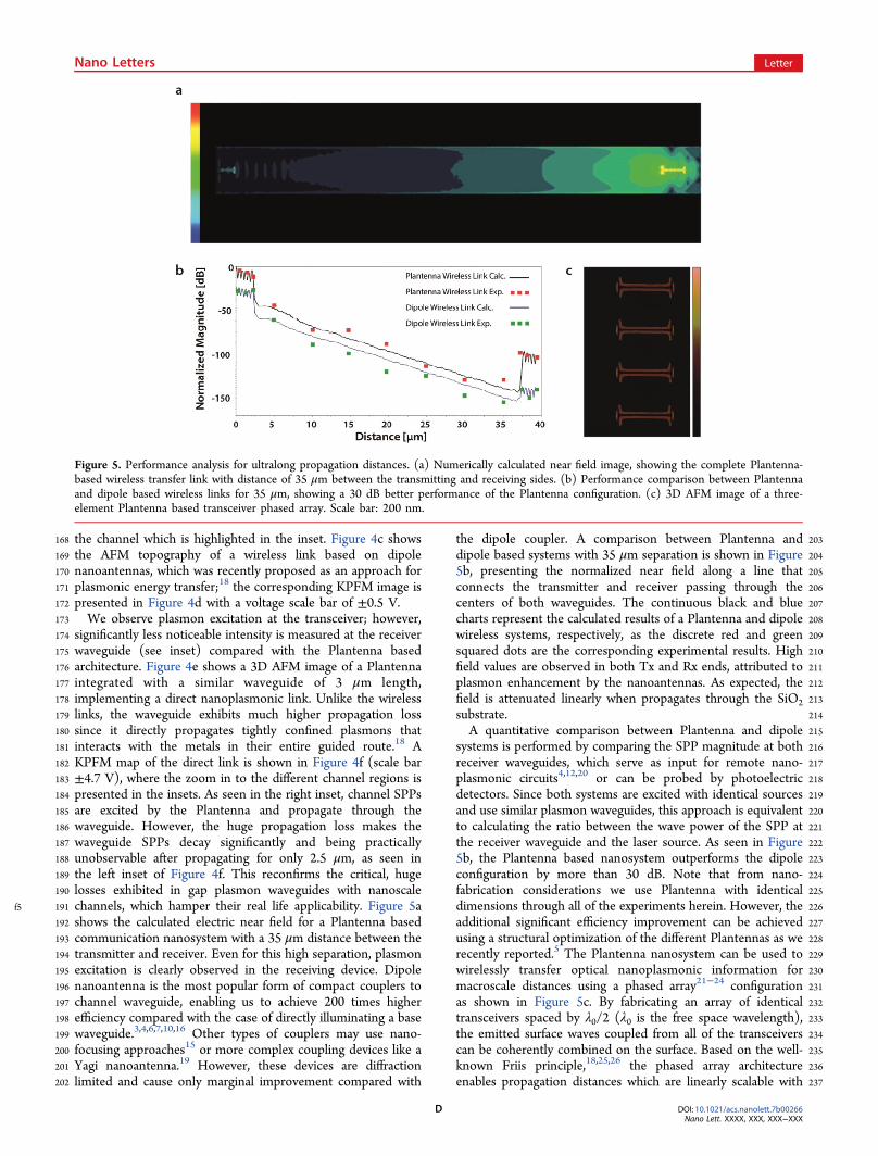
f5 191 channels, which hamper their real life applicability. Figure 5a192 shows the calculated electric near field for a Plantenna based193 communication nanosystem with a 35 μm distance between the194 transmitter and receiver. Even for this high separation, plasmon195 excitation is clearly observed in the receiving device. Dipole196 nanoantenna is the most popular form of compact couplers to197 channel waveguide, enabling us to achieve 200 times higher198 efficiency compared with the case of directly illuminating a base199 waveguide.3,4,6,7,10,16 Other types of couplers may use nano-200 focusing approaches15 or more complex coupling devices like a201 Yagi nanoantenna.19 However, these devices are diffraction202 limited and cause only marginal improvement compared with
203the dipole coupler. A comparison between Plantenna and204dipole based systems with 35 μm separation is shown in Figure2055b, presenting the normalized near field along a line that206connects the transmitter and receiver passing through the207centers of both waveguides. The continuous black and blue208charts represent the calculated results of a Plantenna and dipole209wireless systems, respectively, as the discrete red and green210squared dots are the corresponding experimental results. High211field values are observed in both Tx and Rx ends, attributed to212plasmon enhancement by the nanoantennas. As expected, the213field is attenuated linearly when propagates through the SiO2214substrate.215A quantitative comparison between Plantenna and dipole216systems is performed by comparing the SPP magnitude at both217receiver waveguides, which serve as input for remote nano-218plasmonic circuits4,12,20 or can be probed by photoelectric219detectors. Since both systems are excited with identical sources220and use similar plasmon waveguides, this approach is equivalent221to calculating the ratio between the wave power of the SPP at222the receiver waveguide and the laser source. As seen in Figure2235b, the Plantenna based nanosystem outperforms the dipole224configuration by more than 30 dB. Note that from nano-225fabrication considerations we use Plantenna with identical226dimensions through all of the experiments herein. However, the227additional significant efficiency improvement can be achieved228using a structural optimization of the different Plantennas as we229recently reported.5 The Plantenna nanosystem can be used to230wirelessly transfer optical nanoplasmonic information for231macroscale distances using a phased array21−24 configuration232as shown in Figure 5c. By fabricating an array of identical233transceivers spaced by λ0/2 (λ0 is the free space wavelength),234the emitted surface waves coupled from all of the transceivers235can be coherently combined on the surface. Based on the well-236known Friis principle,18,25,26 the phased array architecture237enables propagation distances which are linearly scalable with
Figure 5. Performance analysis for ultralong propagation distances. (a) Numerically calculated near field image, showing the complete Plantenna-based wireless transfer link with distance of 35 μm between the transmitting and receiving sides. (b) Performance comparison between Plantennaand dipole based wireless links for 35 μm, showing a 30 dB better performance of the Plantenna configuration. (c) 3D AFM image of a three-element Plantenna based transceiver phased array. Scale bar: 200 nm.
Nano Letters Letter
DOI: 10.1021/acs.nanolett.7b00266Nano Lett. XXXX, XXX, XXX−XXX
D

238 the number of transceivers, paving the way toward efficient239 wireless nanoplasmonic data and energy transfer for millimeter240 distances and beyond.241 In conclusion, we designed, fabricated, and experimentally242 characterized a novel high-efficiency nanosystem, capable to243 wirelessly transfer deeply confined optical plasmon polaritons244 for chip−scale distances. Our system is architectured for the245 efficient conversion of nanoscopic SPPs to propagating surface246 waves and to re-excite SPPs from these surface waves at247 significantly remote distances. We demonstrate the trans-248 mission of optical SPPs in channel waveguides with a cross249 section of only 20 nm × 20 nm, for distances which are 3250 orders of magnitude larger than the plasmon wavelength. On251 the basis of the Plantenna, a new generation of high-252 performance nanoantennas with no RF equivalents, our253 nanosystem hugely outperforms both direct and wireless links254 based on dipole nanoantennas by more than 30 dB. For the first255 time, we use a unique combination of scanning probe256 microscopies to create complete real-space near-field mapping257 of a long-range nanoplasmonic wireless link at a high spatial258 resolution. This nanoimaging amalgamation provides valuable259 synergy needed for mapping both nanoscopic plasmon260 polaritons as well as macroscopically propagating surface261 waves. In the quest for reconciling the dimensional mismatch262 between diffraction-limited photonics and integrated elec-263 tronics, our results enable new horizons for high integration264 densities of optical functionalities and interconnects. By using265 phased array configuration and utilizing degrees of freedom in266 polarization, frequency and code domains, inter- and intra-chip267 communications based on ultrafast nanoscale light waves as268 information carriers can now achieve record performances in269 terms of speed distance and size. The presented approach of270 hybridizing Plantenna and channel plasmon waveguides as271 nanotransceivers is immediately applicable for exploring long-272 range interaction between single and multiple quantum273 emitters, while our nanoimaging methodology enables274 enhanced understanding of exciting near-field phenomena at275 the nanoscale.276 Methods. AFM and KPFM Measurements. All measure-277 ments were performed at room temperature and free ambient278 conditions (no vacuum), using a Dimension Icon AFM system279 with a NanoScope V controller (Bruker). For both AFM and280 KPFM measurements, we used NanoWorld probes SSS-NCH281 (SuperSharpSilicon, Noncontact/Tapping mode, High reso-282 nance frequency), with a typical diameter of 2 nm, resonance283 frequency of 320 kHz, and spring constant of 42 N/m.284 Typically, voltages of 2 V, AC capacitance frequencies of 880285 MHz, lift heights of 30−50 nm, and line rates of 0.1 kHz were286 employed. To map the CPD of the sample, we apply both AC287 voltage (VAC) and DC voltage (VDC) to the AFM tip. VAC288 generates oscillating electrical forces between the AFM tip and289 sample surface, and VDC nullifies the oscillating electrical290 forces that originated from CPD between tip and sample291 surface.292 Optical Near-Field Measurements. The optical character-293 ization of the plasmonic structures was performed by a294 MultiView 2000 scanning probe microscope/NSOM system295 (Nanonics Imaging Ltd.). The SPM head was placed on the296 stage of an Olympus dual microscope while remaining the297 optical axis free from above and below. Such a configuration298 allowed us to bring the cantilevered NSOM tip to the desired299 position on the sample under an upper objective of 50×. The300 sample was illuminated with a Liconix diode laser of 785 laser
301CW light from the bottom and focused on a sample with a 50×302objective. We used the bottom piezo scanner of the scanning303head to place the desired structures of the sample very304accurately relatively to the incoming light of the laser from305below. The scan was performed with upper piezo scanner306allowing moving only the NSOM tip while the sample remains307still. The collection of near field light distribution on the surface308was performed in tapping mode with a 200 nm aperture309NSOM tips based tuning fork produced by Super Tips310(Nanonics Imaging Ltd.). The signal was transmitted through311a multimode optical fiber onto an APD. The AFM and NSOM312images were collected simultaneously during the scan, allowing313to monitor the topography of the desired structure and to314correlate it with the near-field optical signal that comes from315any particular feature.316Numerical Simulations. The numerical results are obtained317by using the software package ANSYS HFSS V15, the industry-318standard simulation tool for 3D full-wave electromagnetic field319simulation. HFSS solves Maxwell’s equations via the finite320element method (FEM) using an adaptive mesh refinement321process for tailored accuracy requirements. The field’s solutions322are calculated with the metallic (Ag) plasmonic structures being323deposited on a homogeneous SiO2 substrate. The nanoantenna324is illuminated by optical sources at 474 THz (wavelength of325633 nm), which are modeled as focused Gaussian beams with 1326μm characteristic diameter. The electric field is polarized in327parallel with the dipole direction, as the wave vector K is328perpendicular. A selectively dense meshing is assigned in the329metallic and waveguiding regions, with a maximum cell size of 1330nm and 750 000 FEM tetrahedral cells. To provide maximum331accuracy, the model is terminated as following: the interface332with free space is bounded by perfectly matched layer (PML)333absorbing boundary conditions (ABC), while the metallic and334SiO2 termination are done via layered impedance (LI) ABC.335The minimum number of adaptive meshing iterations was set336to 12, with a convergence condition of 1% maximum energy337variance between adjacent iterations.338Fabrication. SiO2/Si sample was spin-coated with poly-339(methyl methacrylate) (PMMA 950 A2) electron-beam resist340providing thickness of 100 nm. The samples coated with341PMMA were subsequently baked for 120 s on a hot plate at342180C. The desired pattern was exposed in the PMMA layer343using a CRESTEC CABLE-9000C high-resolution electron-344beam lithography system using different doses to control line345and gap width. Then the samples were developed for 90 s using346methyl isobutyl ketone (MIBK) and rinsed with IPA. The347samples were subsequently exposed to Ar plasma to etch 10 nm348in order to remove leftovers from the pattern, sputtered using349BESTEC 2″ DC magnetron to deposit 2 nm Cr and 18 nm Au,350and then immersed in 180 Khz ultrasonic bath with NMP for 3351h for resist liftoff.
352■ AUTHOR INFORMATION353Corresponding Author354*E-mail: [email protected].
355ORCID356Moshik Cohen: 0000-0002-7519-9742357Author Contributions358M.C. carried out the theoretical design and analysis, designed359the studies, performed the experiments, and wrote the360manuscript. Z.Z. and R.S. participated in writing the manuscript361and designing the study.
Nano Letters Letter
DOI: 10.1021/acs.nanolett.7b00266Nano Lett. XXXX, XXX, XXX−XXX
E
362 Notes363 The authors declare no competing financial interest.
364 ■ ACKNOWLEDGMENTS365 M.C. acknowledges Olga Girshevitz Yafit from Bar-Ilan366 Institute for Nanotechnology & Advanced Materials (BINA),367 for the support in fabricating the reported structures.
368 ■ REFERENCES(1)369 Schuller, J. A.; Barnard, E. S.; Cai, W.; Jun, Y. C.; White, J. S.;
370 Brongersma, M. L. Nat. Mater. 2010, 9 (3), 193−204.(2)371 Brongersma, M. L.; Shalaev, V. M. Science 2010, 328 (5977),
372 440−441.(3)373 Cohen, M.; Shavit, R.; Zalevsky, Z. Sci. Rep. 2015, 4, 04096.(4)374 Cohen, M.; Zalevsky, Z.; Shavit, R. Nanoscale 2013, 5 (12),
375 5442−5449.(5)376 Cohen, M.; Shavit, R.; Zalevsky, Z. Sci. Rep. 2015, 5, 17562.(6)377 Cohen, M.; Shavit, R.; Zalevsky, Z. In Planar Waveguides and
378 other Confined Geometries; Marowsky, G., Ed.; Springer Series in379 Optical Sciences; Springer: New York, 2015; pp 45−66.
(7)380 Dionne, J. A.; Sweatlock, L. A.; Atwater, H. A.; Polman, A. Phys.381 Rev. B: Condens. Matter Mater. Phys. 2006, 73 (3), 035407.
(8)382 Bozhevolnyi, S. I.; Volkov, V. S.; Devaux, E.; Laluet, J.-Y.;383 Ebbesen, T. W. Nature 2006, 440 (7083), 508−511.
(9)384 Dregely, D.; Lindfors, K.; Lippitz, M.; Engheta, N.; Totzeck, M.;385 Giessen, H. Nat. Commun. 2014, 5, 4354.
(10)386 Cohen, M.; Abulafia, Y.; Shavit, R.; Zalevsky, Z. ACS Nano387 2017, 11, 3274.
(11)388 Carmeli, I.; Cohen, M.; Heifler, O.; Lilach, Y.; Zalevsky, Z.;389 Mujica, V.; Richter, S. Nat. Commun. 2015, 6, 7334.
(12)390 Cohen, M.; Shavit, R.; Zalevsky, Z.; Abulafia, Y. In CLEO: 2014;391 OSA Technical Digest (online); Optical Society of America, 2014; p392 JTu4A.135.
(13)393 Lu, H.; Liu, X.; Wang, G.; Mao, D. Nanotechnology 2012, 23394 (44), 444003.
(14)395 Wang, S.; Zhan, Q. Sci. Rep. 2016, 6, 29626.(15)396 Choo, H.; Kim, M.-K.; Staffaroni, M.; Seok, T. J.; Bokor, J.;
397 Cabrini, S.; Schuck, P. J.; Wu, M. C.; Yablonovitch, E. Nat. Photonics398 2012, 6 (12), 838−844.
(16)399 Wen, J.; Romanov, S.; Peschel, U. Opt. Express 2009, 17 (8),400 5925−5932.
(17)401 Andryieuski, A.; Zenin, V. A.; Malureanu, R.; Volkov, V. S.;402 Bozhevolnyi, S. I.; Lavrinenko, A. V. Nano Lett. 2014, 14 (7), 3925−403 3929.
(18)404 Alu,̀ A.; Engheta, N. Phys. Rev. Lett. 2010, 104 (21), 213902.(19)405 Solís, D. M.; Taboada, J. M.; Obelleiro, F.; Landesa, L. Opt.
406 Express 2013, 21 (2), 2369−2377.(20)407 Dionne, J. A.; Sweatlock, L. A.; Sheldon, M. T.; Alivisatos, A. P.;
408 Atwater, H. A. IEEE J. Sel. Top. Quantum Electron. 2010, 16 (1), 295−409 306.
(21)410 Abediasl, H.; Hashemi, H. Opt. Express 2015, 23 (5), 6509−411 6519.
(22)412 Cohen, E.; Ruberto, M.; Cohen, M.; Degani, O.; Ravid, S.;413 Ritter, D. IEEE Trans. Microwave Theory Tech. 2013, 61 (3), 1359−414 1375.
(23)415 Sun, J.; Timurdogan, E.; Yaacobi, A.; Hosseini, E. S.; Watts, M.416 R. Nature 2013, 493 (7431), 195−199.
(24)417 Maguid, E.; Yulevich, I.; Veksler, D.; Kleiner, V.; Brongersma,418 M. L.; Hasman, E. Science 2016, 352, 1202.
(25)419 Choi, H. S.; Kang, S. Y.; Cho, S. J.; Oh, I.-Y.; Shin, M.; Park, H.;420 Jang, C.; Min, B.-C.; Kim, S.-I.; Park, S.-Y.; Park, C. S. Sci. Rep. 2015, 4,421 5486.
(26)422 Yang, Y.; Li, Q.; Qiu, M. Sci. Rep. 2016, 6, 19490.
Nano Letters Letter
DOI: 10.1021/acs.nanolett.7b00266Nano Lett. XXXX, XXX, XXX−XXX
F