WIRELESS & SENSING
92
SX1211 Transceiver Ultra-Low Power Integrated UHF Transceiver WIRELESS & SENSING Rev 8– February 2013 Page 1 of 92 www.semtech.com General Description The SX1211 is a low cost single-chip transceiver operating in the frequency ranges from 863-870, 902- 928 MHz and 950-960 MHz. The SX1211 is optimized for very low power consumption (3mA in receiver mode). It incorporates a baseband modem with data rates up to 200 kb/s. Data handling features include a sixty-four byte FIFO, packet handling, automatic CRC generation and data whitening. Its highly integrated architecture allows for minimum external component count whilst maintaining design flexibility. All major RF communication parameters are programmable and most of them may be dynamically set. It complies with European (ETSI EN 300-220 V2.1.1) and North American (FCC part 15.247 and 15.249) regulatory standards. Ordering Information Table 1: Ordering Information Part number Delivery Minimum Order Quantity / Multiple SX1211I084TRT Tape & Reel 3000 pieces SX1211I084T Tray 200 pieces SX1211WS Wafer 1 wafer TQFN-32 package – Operating range [-40;+85°C] T refers to Lead Free packaging This device is WEEE and RoHS compliant Features Low Rx power consumption: 3mA Low Tx power consumption: 25 mA @ +10 dBm Good reception sensitivity: down to -107 dBm at 25 kb/s in FSK, -113 dBm at 2kb/s in OOK Programmable RF output power: up to +12.5 dBm in 8 steps Packet handling feature with data whitening and automatic CRC generation Wide RSSI (Received Signal Strength Indicator) dynamic range, 70dB from Rx noise floor Bit rates up to 200 kb/s, NRZ coding On-chip frequency synthesizer FSK and OOK modulation Incoming sync word recognition Built-in Bit-Synchronizer for incoming data and clock synchronization and recovery 5 x 5 mm TQFN package Optimized Circuit Configuration for Low-cost applications Applications Wireless alarm and security systems Wireless sensor networks Automated Meter Reading Home and building automation Industrial monitoring and control Remote Wireless Control Application Circuit Schematic
Transcript of WIRELESS & SENSING

SX1211 TransceiverUltra-Low Power Integrated UHF Transceiver
WIRELESS & SENSING
Rev 8– February 2013 Page 1 of 92 www.semtech.com
General Description The SX1211 is a low cost single-chip transceiver operating in the frequency ranges from 863-870, 902-928 MHz and 950-960 MHz. The SX1211 is optimized for very low power consumption (3mA in receiver mode). It incorporates a baseband modem with data rates up to 200 kb/s. Data handling features include a sixty-four byte FIFO, packet handling, automatic CRC generation and data whitening. Its highly integrated architecture allows for minimum external component count whilst maintaining design flexibility. All major RF communication parameters are programmable and most of them may be dynamically set. It complies with European (ETSI EN 300-220 V2.1.1) and North American (FCC part 15.247 and 15.249) regulatory standards.
Ordering Information Table 1: Ordering Information
Part number Delivery Minimum Order Quantity / Multiple
SX1211I084TRT Tape & Reel 3000 pieces
SX1211I084T Tray 200 pieces
SX1211WS Wafer 1 wafer TQFN-32 package – Operating range [-40;+85°C] T refers to Lead Free packaging This device is WEEE and RoHS compliant
Features Low Rx power consumption: 3mA Low Tx power consumption: 25 mA @ +10 dBm Good reception sensitivity: down to -107 dBm at
25 kb/s in FSK, -113 dBm at 2kb/s in OOK Programmable RF output power: up to +12.5 dBm
in 8 steps Packet handling feature with data whitening and
automatic CRC generation Wide RSSI (Received Signal Strength Indicator)
dynamic range, 70dB from Rx noise floor Bit rates up to 200 kb/s, NRZ coding On-chip frequency synthesizer FSK and OOK modulation Incoming sync word recognition Built-in Bit-Synchronizer for incoming data and
clock synchronization and recovery 5 x 5 mm TQFN package Optimized Circuit Configuration for Low-cost
applications
Applications Wireless alarm and security systems Wireless sensor networks Automated Meter Reading Home and building automation Industrial monitoring and control Remote Wireless Control
Application Circuit Schematic
SX1211
WIRELESS & SENSING
Rev 8 – February 2013 Page 2 of 92 www.semtech.com
Table of Contents 1. General Description ................................................................... 5 1.1. Simplified Block Diagram ........................................................ 5 1.2. Pin Diagram ............................................................................ 6 1.3. Pin Description ........................................................................ 7 2. Electrical Characteristics ............................................................ 8 2.1. ESD Notice.............................................................................. 8 2.2. Absolute Maximum Ratings .................................................... 8 2.3. Operating Range ..................................................................... 8 2.4. Chip Specification ................................................................... 8 2.4.1. Power Consumption ............................................................. 8 2.4.2. Frequency Synthesis ........................................................... 9 2.4.3. Transmitter ........................................................................... 9 2.4.4. Receiver ............................................................................. 10 2.4.5. Digital Specification ............................................................ 11 3. Architecture Description ........................................................... 12 3.1. Power Supply Strategy.......................................................... 12 3.2. Frequency Synthesis Description ......................................... 13 3.2.1. Reference Oscillator .......................................................... 13 3.2.2. CLKOUT Output ................................................................. 13 3.2.3. PLL Architecture ................................................................ 14 3.2.4. PLL Tradeoffs..................................................................... 14 3.2.5. Voltage Controlled Oscillator ............................................. 15 3.2.6. PLL Loop Filter ................................................................... 16 3.2.7. PLL Lock Detection Indicator ............................................. 16 3.2.8. Frequency Calculation ....................................................... 16 3.3. Transmitter Description ......................................................... 18 3.3.1. Architecture Description ..................................................... 18 3.3.2. Bit Rate Setting .................................................................. 19 3.3.3. Alternative Settings ............................................................ 19 3.3.4. Fdev Setting in FSK Mode ................................................. 19 3.3.5. Fdev Setting in OOK Mode ................................................ 19 3.3.6. Interpolation Filter .............................................................. 20 3.3.7. Power Amplifier .................................................................. 20 3.3.8. Common Input and Output Front-End ................................ 22 3.4. Receiver Description ............................................................. 23 3.4.1. Architecture ........................................................................ 23 3.4.2. LNA and First Mixer ........................................................... 24 3.4.3. IF Gain and Second I/Q Mixer ........................................... 24 3.4.4. Channel Filters ................................................................... 24 3.4.5. Channel Filters Setting in FSK Mode ................................. 25 3.4.6. Channel Filters Setting in OOK Mode ................................ 26 3.4.7. RSSI ................................................................................... 26 3.4.8. Fdev Setting in Receive Mode ........................................... 28 3.4.9. FSK Demodulator .............................................................. 28 3.4.10. OOK Demodulator ........................................................... 28 3.4.11. Bit Synchronizer ............................................................... 31 3.4.12. Alternative Settings .......................................................... 32 3.4.13. Data Output ...................................................................... 32 4. Operating Modes...................................................................... 33 4.1. Modes of Operation .............................................................. 33 4.2. Digital Pin Configuration vs. Chip Mode ............................... 33 5. Data Processing ....................................................................... 34 5.1. Overview ............................................................................... 34 5.1.1. Block Diagram .................................................................... 34 5.1.2. Data Operation Modes ....................................................... 34 5.2. Control Block Description ...................................................... 35 5.2.1. SPI Interface ...................................................................... 35 5.2.2. FIFO ................................................................................... 38 5.2.3. Sync Word Recognition ..................................................... 40 5.2.4. Packet Handler................................................................... 40 5.2.5. Control ................................................................................ 40 5.3. Continuous Mode .................................................................. 41
5.3.1. General Description ............................................................41 5.3.2. Tx Processing .....................................................................41 5.3.3. Rx Processing .....................................................................42 5.3.4. Interrupt Signals Mapping ...................................................42 5.3.5. uC Connections ..................................................................43 5.3.6. Continuous Mode Example .................................................43 5.4. Buffered Mode .......................................................................44 5.4.1. General Description ............................................................44 5.4.2. Tx Processing .....................................................................44 5.4.3. Rx Processing .....................................................................45 5.4.4. Interrupt Signals Mapping ...................................................46 5.4.5. uC Connections ..................................................................47 5.4.6. Buffered Mode Example .....................................................47 5.5. Packet Mode ..........................................................................49 5.5.1. General Description ............................................................49 5.5.2. Packet Format .....................................................................49 5.5.3. Tx Processing .....................................................................51 5.5.4. Rx Processing .....................................................................51 5.5.5. Packet Filtering ...................................................................52 5.5.6. DC-Free Data Mechanisms ................................................53 5.5.7. Interrupt Signal Mapping .....................................................54 5.5.8. uC Connections ..................................................................55 5.5.9. Packet Mode Example ........................................................56 5.5.10. Additional Information .......................................................56 6. Configuration and Status Registers ..........................................58 6.1. General Description ...............................................................58 6.2. Main Configuration Register - MCParam ...............................58 6.3. Interrupt Configuration Parameters - IRQParam ...................60 6.4. Receiver Configuration parameters - RXParam ....................62 6.5. Sync Word Parameters - SYNCParam ..................................63 6.6. Transmitter Parameters - TXParam .......................................64 6.7. Oscillator Parameters - OSCParam .......................................64 6.8. Packet Handling Parameters – PKTParam ............................65 7. Application Information .............................................................66 7.1. Crystal Resonator Specification .............................................66 7.2. Software for Frequency Calculation .......................................66 7.2.1. GUI ......................................................................................66 7.2.2. .dll for Automatic Production Bench ....................................66 7.3. Switching Times and Procedures ..........................................66 7.3.1. Optimized Receive Cycle ....................................................67 7.3.2. Optimized Transmit Cycle ...................................................68 7.3.3. Transmitter Frequency Hop Optimized Cycle .....................69 7.3.4. Receiver Frequency Hop Optimized Cycle .........................70 7.3.5. Rx Tx and Tx Rx Jump Cycles .......................................71 7.4. Reset of the Chip ...................................................................72 7.4.1. POR ....................................................................................72 7.4.2. Manual Reset ......................................................................72 7.5. Reference Design ..................................................................73 7.5.1. Application Schematic .........................................................73 7.5.2. PCB Layout .........................................................................73 7.5.3. Bill Of Material .....................................................................74 7.5.4. SAW Filter Plot ....................................................................75 7.5.5. Ordering Information for Tools ............................................75 7.6. Reference Design Performance .............................................76 7.6.1. Sensitivity Flatness .............................................................77 7.6.2. Sensitivity vs. LO Drift .........................................................78 7.6.3. Sensitivity vs. Receiver BW ................................................79 7.6.4. Sensitivity Stability over Temperature and Voltage ............80 7.6.5. Sensitivity vs. Bit Rate ........................................................80 7.6.6. Adjacent Channel Rejection ................................................81 7.6.7. Output Power Flatness .......................................................82 7.6.8. Pout and IDD vs. PA Setting ...............................................83

SX1211
WIRELESS & SENSING
Rev 8 – February 2013 Page 3 of 92 www.semtech.com
7.6.9. Pout Stability over Temperature and Voltage .................... 84 7.6.10. Transmitter Spectral Purity .............................................. 85 7.6.11. OOK Channel Bandwidth ................................................. 86 7.6.12. FSK Spectrum in Europe ................................................. 87 7.6.13. Digital Modulation Schemes ............................................ 88 7.6.14. Current Stability over Temperature and Voltage .............. 89
8. Packaging Information ..............................................................90 8.1. Package Outline Drawing ......................................................90 8.2. PCB Land Pattern ..................................................................90 8.3. Tape & Reel Specification ......................................................91 9. Revision History ........................................................................92 10. Contact Information .................................................................92
Index of Figures Figure 1: SX1211 Simplified Block Diagram .................................. 5 Figure 2: SX1211 Pin Diagram ...................................................... 6 Figure 3: SX1211 Detailed Block Diagram .................................. 12 Figure 4: Power Supply Breakdown ............................................. 13 Figure 5: Frequency Synthesizer Description .............................. 14 Figure 6: LO Generator ................................................................ 14 Figure 7: Loop Filter ..................................................................... 16 Figure 8: Transmitter Architecture ............................................... 18 Figure 9: I(t), Q(t) Overview ......................................................... 18 Figure 10: PA Control................................................................... 21 Figure 11: Optimal Load Impedance Chart .................................. 21 Figure 12: Recommended PA Biasing and Output Matching ..... 22 Figure 13: Front-end Description ................................................. 22 Figure 14: Receiver Architecture ................................................. 23 Figure 15: FSK Receiver Setting ................................................. 23 Figure 16: OOK Receiver Setting ................................................ 23 Figure 17: Active Channel Filter Description ................................ 24 Figure 18: Butterworth Filter's Actual BW .................................... 26 Figure 19: Polyphase Filter's Actual BW ...................................... 26 Figure 20: RSSI Dynamic Range ................................................. 27 Figure 21: RSSI IRQ Timings ...................................................... 28 Figure 22: OOK Demodulator Description ................................... 29 Figure 23: Floor Threshold Optimization ...................................... 30 Figure 24: BitSync Description ..................................................... 31 Figure 25: SX1211’s Data Processing Conceptual View ............. 34 Figure 26: SPI Interface Overview and uC Connections ............. 35 Figure 27: Write Register Sequence ............................................ 36 Figure 28: Read Register Sequence ............................................ 37 Figure 29: Write Bytes Sequence (ex: 2 bytes) ........................... 37 Figure 30: Read Bytes Sequence (ex: 2 bytes) ........................... 38 Figure 31: FIFO and Shift Register (SR) ...................................... 38 Figure 32: FIFO Threshold IRQ Source Behavior ........................ 39 Figure 33: Sync Word Recognition .............................................. 40 Figure 34: Continuous Mode Conceptual View ............................ 41 Figure 35: Tx Processing in Continuous Mode ............................ 41 Figure 36: Rx Processing in Continuous Mode ............................ 42 Figure 37: uC Connections in Continuous Mode ......................... 43 Figure 38: Buffered Mode Conceptual View ................................ 44 Figure 39: Tx processing in Buffered Mode ................................. 45 Figure 40: Rx Processing in Buffered Mode ................................ 46 Figure 41: uC Connections in Buffered Mode .............................. 47 Figure 42: Packet Mode Conceptual View ................................... 49 Figure 43: Fixed Length Packet Format ....................................... 50 Figure 44: Variable Length Packet Format .................................. 51 Figure 45: CRC Implementation .................................................. 53
Figure 46: Manchester Encoding/Decoding ..................................54 Figure 47: Data Whitening ............................................................54 Figure 48: uC Connections in Packet Mode .................................55 Figure 49: Optimized Rx Cycle .....................................................67 Figure 50: Optimized Tx Cycle ......................................................68 Figure 51: Tx Hop Cycle ...............................................................69 Figure 52: Rx Hop Cycle ...............................................................70 Figure 53: Rx Tx Rx Cycle ...................................................71 Figure 54: POR Timing Diagram ...................................................72 Figure 55: Manual Reset Timing Diagram ....................................72 Figure 56: Reference Design Circuit Schematic ...........................73 Figure 57: Reference Design‘s Stackup .......................................74 Figure 58: Reference Design Layout (top view) ............................74 Figure 59: 915 MHz SAW Filter Plot .............................................75 Figure 60: 869 MHz SAW Filter Plot .............................................75 Figure 61: Sensitivity Across the 868 MHz Band ..........................77 Figure 62: Sensitivity Across the 915 MHz Band ..........................77 Figure 63: FSK Sensitivity Loss vs. LO Drift .................................78 Figure 64: OOK Sensitivity Loss vs. LO Drift ................................78 Figure 65: FSK Sensitivity vs. Rx BW ...........................................79 Figure 66: OOK Sensitivity Change vs. Rx BW ............................79 Figure 67: Sensitivity Stability .......................................................80 Figure 68: FSK Sensitivity vs. BR .................................................80 Figure 69: OOK Sensitivity vs. BR ................................................81 Figure 70: ACR in FSK Mode .......................................................81 Figure 71: ACR in OOK Mode ......................................................82 Figure 72: Pout for 869 MHz Band Operation ...............................82 Figure 73: Pout for 915 MHz Band Operation ...............................83 Figure 74: Pout and IDD at all PA Settings, 869 MHz ..................83 Figure 75: Pout and IDD at all PA Settings, 915 MHz ..................84 Figure 76: Pout Stability ................................................................84 Figure 77: 869 MHz Spectral Purity DC-1GHz .............................85 Figure 78: 869 MHz Spectral Purity 1-6GHz .................................85 Figure 79: OOK Spectrum - 2kbps ................................................86 Figure 80: OOK Spectrum - 8kbps ................................................86 Figure 81: OOK Spectrum - 16.7kbps ...........................................86 Figure 82: FSK - 1.56kbps - +/-33 kHz .........................................87 Figure 83: FSK - 25 kbps - +/-50 kHz ...........................................87 Figure 84: FSK - 40 kbps - +/-40 kHz ...........................................87 Figure 85: DTS 6dB Bandwidth ....................................................88 Figure 86: DTS Power Spectral Density .......................................88 Figure 87: IDD vs. Temp and VDD ...............................................89 Figure 88: Package Outline Drawing ............................................90 Figure 89: PCB Land Pattern ........................................................90 Figure 90: Tape & Reel Dimensions .............................................91

SX1211
WIRELESS & SENSING
Rev 8 – February 2013 Page 4 of 92 www.semtech.com
Index of Tables Table 1: Ordering Information ........................................................ 1 Table 2: SX1211 Pinouts ............................................................... 7 Table 3: Absolute Maximum Ratings ............................................. 8 Table 4: Operating Range .............................................................. 8 Table 5: Power Consumption Specification ................................... 8 Table 6: Frequency Synthesizer Specification ............................... 9 Table 7: Transmitter Specification ................................................. 9 Table 8: Receiver Specification.................................................... 10 Table 9: Digital Specification ........................................................ 11 Table 10: MCParam_Freq_band Setting ..................................... 15 Table 11: PA Rise/Fall Times....................................................... 20 Table 12: Operating Modes ......................................................... 33 Table 13: Pin Configuration vs. Chip Mode ................................. 33 Table 14: Data Operation Mode Selection ................................... 35 Table 15: Config vs. Data SPI Interface Selection ....................... 36 Table 16: Status of FIFO when Switching Between Different Modes of the Chip ........................................................................ 39 Table 17: Interrupt Mapping in Continuous Rx Mode .................. 42 Table 18: Interrupt Mapping in Continuous Tx Mode ................... 42 Table 19: Relevant Config. Registers in Continuous Mode ........ 43
Table 20: Interrupt Mapping in Buffered Rx and Stby Modes .......46 Table 21: Interrupt Mapping in Buffered Tx Mode ........................46 Table 22: Relevant Configuration Registers in Buffered Mode .....47 Table 23: Interrupt Mapping in Rx and Stby in Packet Mode ........55 Table 24: Interrupt Mapping in Tx Packet Mode ...........................55 Table 25: Relevant Configuration Registers in Packet Mode .......56 Table 26: Registers List ................................................................58 Table 27: MCParam Register Description ....................................58 Table 28: IRQParam Register Description ....................................60 Table 29: RXParam Register Description .....................................62 Table 30: SYNCParam Register Description ................................63 Table 31: TXParam Register Description .....................................64 Table 32: OSCParam Register Description ..................................64 Table 33: PKTParam Register Description ...................................65 Table 34: Crystal Resonator Specification ....................................66 Table 35: Reference Design BOM ................................................74 Table 36: Tools Ordering Information ...........................................75 Table 37: FSK Rx Filters vs. Bit Rate ...........................................76 Table 38: OOK Rx Filters vs. Bit Rate ..........................................76
Acronyms BOM Bill Of Materials BR Bit Rate BW Bandwidth
CCITT Comité Consultatif International Téléphonique et Télégraphique - ITU
CP Charge Pump CRC Cyclic Redundancy Check DAC Digital to Analog Converter DDS Direct Digital Synthesis DLL Dynamically Linked Library ERP Equivalent Radiated Power
ETSI European Telecommunications Standards Institute
FCC Federal Communications Commission Fdev Frequency Deviation FIFO First In First Out FS Frequency Synthesizer FSK Frequency Shift Keying GUI Graphical User Interface IC Integrated Circuit ID IDentificator IF Intermediate Frequency IRQ Interrupt ReQuest ITU International Telecommunication Union LFSR Linear Feedback Shift Register LNA Low Noise Amplifier
LO Local Oscillator LSB Least Significant Bit MSB Most Significant Bit NRZ Non Return to Zero NZIF Near Zero Intermediate Frequency OOK On Off Keying PA Power Amplifier PCB Printed Circuit Board PFD Phase Frequency Detector PLL Phase-Locked Loop POR Power On Reset RBW Resolution BandWidth RF Radio Frequency RSSI Received Signal Strength Indicator Rx Receiver SAW Surface Acoustic Wave SPI Serial Peripheral Interface SR Shift Register Stby Standby Tx Transmitter uC Microcontroller VCO Voltage Controlled Oscillator XO Crystal Oscillator XOR eXclusive OR
SX1211
WIRELESS & SENSING
Rev 8 – February 2013 Page 5 of 92 www.semtech.com
This product datasheet contains a detailed description of the SX1211 performance and functionality. Please consult the Semtech website for the latest updates or errata.
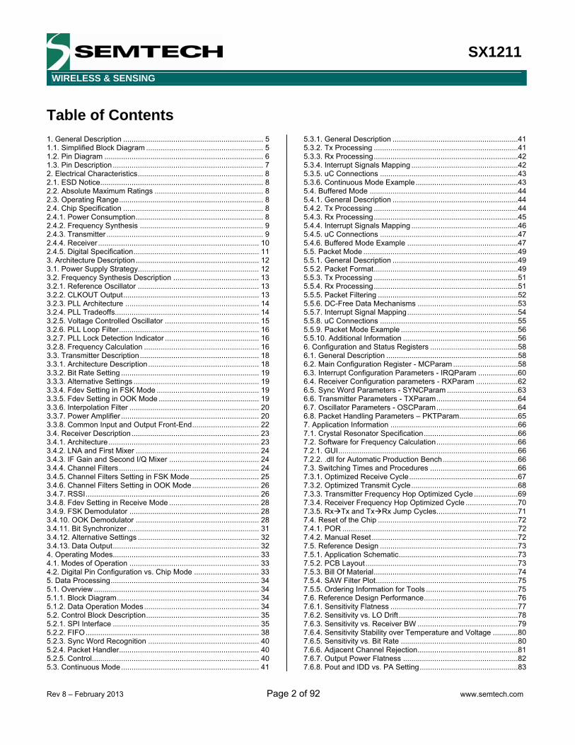
1. General Description The SX1211 is a single chip FSK and OOK transceiver capable of operation in the 863-870 MHz and 902-928 MHz license free ISM frequency bands, as well as the 950 - 960 MHz frequency band. It complies with both the relevant European and North American standards, EN 300-220 V2.1.1 (June 2006 release) and FCC Part 15 (10-1-2006 edition). A unique feature of this circuit is its extremely low current consumption in receiver mode of only 3mA (typ). The SX1211 comes in a 5x5 mm TQFN-32 package.
1.1. Simplified Block Diagram
Figure 1: SX1211 Simplified Block Diagram
SX1211
WIRELESS & SENSING
Rev 8 – February 2013 Page 6 of 92 www.semtech.com
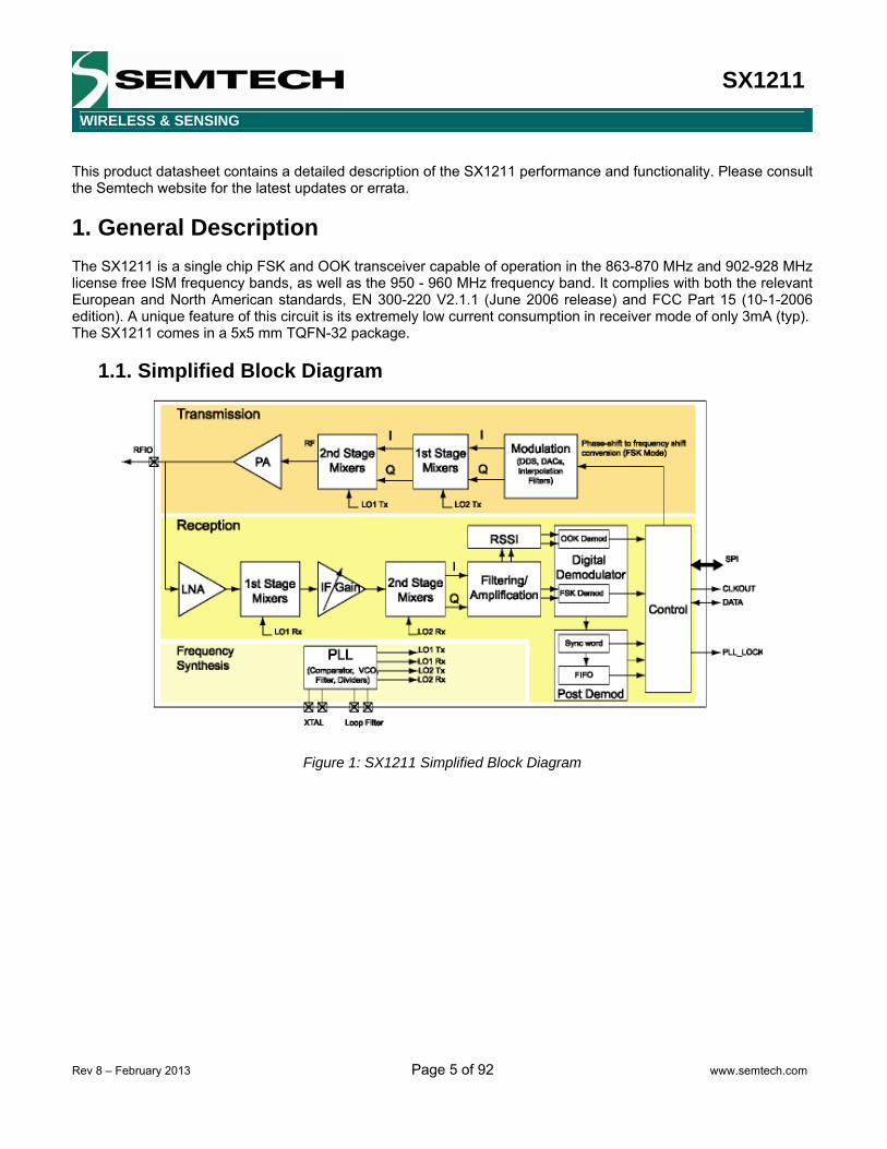
1.2. Pin Diagram The following diagram shows the pins arrangement of the QFN package, top view.
Figure 2: SX1211 Pin Diagram
Notes: yyww refers to the date code ------ refers to the lot number
SX1211
WIRELESS & SENSING
Rev 8 – February 2013 Page 7 of 92 www.semtech.com
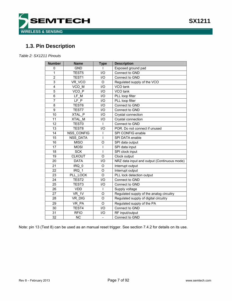
1.3. Pin Description Table 2: SX1211 Pinouts
Number Name Type Description 0 GND I Exposed ground pad 1 TEST5 I/O Connect to GND 2 TEST1 I/O Connect to GND 3 VR_VCO O Regulated supply of the VCO 4 VCO_M I/O VCO tank 5 VCO_P I/O VCO tank 6 LF_M I/O PLL loop filter 7 LF_P I/O PLL loop filter 8 TEST6 I/O Connect to GND 9 TEST7 I/O Connect to GND
10 XTAL_P I/O Crystal connection 11 XTAL_M I/O Crystal connection 12 TEST0 I Connect to GND 13 TEST8 I/O POR. Do not connect if unused 14 NSS_CONFIG I SPI CONFIG enable 15 NSS_DATA I SPI DATA enable 16 MISO O SPI data output 17 MOSI I SPI data input 18 SCK I SPI clock input 19 CLKOUT O Clock output 20 DATA I/O NRZ data input and output (Continuous mode) 21 IRQ_0 O Interrupt output 22 IRQ_1 O Interrupt output 23 PLL_LOCK O PLL lock detection output 24 TEST2 I/O Connect to GND 25 TEST3 I/O Connect to GND 26 VDD I Supply voltage 27 VR_1V O Regulated supply of the analog circuitry 28 VR_DIG O Regulated supply of digital circuitry 29 VR_PA O Regulated supply of the PA 30 TEST4 I/O Connect to GND 31 RFIO I/O RF input/output 32 NC - Connect to GND
Note: pin 13 (Test 8) can be used as an manual reset trigger. See section 7.4.2 for details on its use.
SX1211
WIRELESS & SENSING
Rev 8 – February 2013 Page 8 of 92 www.semtech.com
2. Electrical Characteristics
2.1. ESD Notice The SX1211 is a high performance radio frequency device. It satisfies: Class 2 of the JEDEC standard JESD22-A114-B (Human Body Model), except on pins 3-4-5-27-28-29-31
where it satisfies Class 1A. Class III of the JEDEC standard JESD22-C101C (Charged Device Model) on all pins.
It should thus be handled with all the necessary ESD precautions to avoid any permanent damage.
2.2. Absolute Maximum Ratings Stresses above the values listed below may cause permanent device failure. Exposure to absolute maximum ratings for extended periods may affect device reliability.
Table 3: Absolute Maximum Ratings
2.3. Operating Range Table 4: Operating Range
2.4. Chip Specification Conditions: Temp = 25 °C, VDD = 3.3 V, crystal frequency = 12.8 MHz, carrier frequency = 869 or 915 MHz, modulation FSK, data rate = 25 kb/s, Fdev = 50 kHz, fc = 100 kHz, unless otherwise specified. Note: RF performance depends on assembly. Electrical specifications listed in this section are obtained with the TQFN package described in section 8 “Packaging Information”.
2.4.1. Power Consumption
Table 5: Power Consumption Specification
Symbol Description Conditions Min Typ Max UnitIDDSL Supply current, Sleep mode - 0.1 2 µA
IDDST Supply current in standby mode, CLKOUT disabled Crystal oscillator running(2) - 65 80 µA
IDDFS Supply current in FS mode Frequency synthesizer running - 1.3 1.7 mA
IDDR Supply current in Rx mode - 3.0 3.5 mA
IDDT Supply current in Tx mode Output power = +10 dBm Output power = 1dBm(1)
- -
25 16
30 21
mA mA
Symbol Description Min Max UnitVDDmr Supply voltage -0.3 3.7 V
Tmr Storage temperature -55 125 °C Pmr Input level - 0 dBm
Symbol Description Min Max Unit VDDop Supply Voltage 2.1 3.6 V
Trop Temperature -40 +85 °C ML Input Level - 0 dBm
SX1211
WIRELESS & SENSING
Rev 8 – February 2013 Page 9 of 92 www.semtech.com
(1) Guaranteed by design and characterization (2) Crystal Cload=10pF, C0=2.5pF, Rm=15 Ohms
2.4.2. Frequency Synthesis
Table 6: Frequency Synthesizer Specification
(1) Guaranteed by design and characterization
2.4.3. Transmitter
Table 7: Transmitter Specification
(1) Guaranteed by design and characterization
Symbol Description Conditions Min Typ Max Unit
FR Frequency ranges Programmable but requires specific BOM
863 902 950
- - -
870 928 960
MHz MHz MHz
BR_F Bit rate (FSK) NRZ 1.56 - 200 Kb/s BR_O Bit rate (OOK) NRZ 1.56 - 32 Kb/s FDA Frequency deviation (FSK) 33 50 200 kHz XTAL Crystal oscillator frequency 9 12.8 15 MHz
FSTEP Frequency synthesizer step
Variable, depending on the frequency. - 2 - kHz
TS_OSC Oscillator wake-up time From Sleep mode(1) - 1.5 5 ms
TS_FS
Frequency synthesizer wake-up time at most 10 kHz away from the target
From Stby mode - 500 800 µs
TS_HOP Frequency synthesizer hop time at most 10 kHz away from the target
200 kHz step - 180 - µs 1 MHz step - 200 - µs 5 MHz step - 250 - µs 7 MHz step - 260 - µs 12 MHz step - 290 - µs 20 MHz step - 320 - µs 27 MHz step - 340 - µs
Symbol Description Conditions Min Typ Max Unit
RFOP RF output power, programmable with 8 steps of typ. 3dB
Maximum power setting - +12.5 - dBm
Minimum power setting - -8.5 - dBm
PN Phase noise Measured with a 600 kHz offset, at the transmitter output.
- -112 - dBc/Hz
SPT Transmitted spurious
At any offset between 200 kHz and 600 kHz, unmodulated carrier, Fdev = 50 kHz.
- - -47 dBc
TS_TR(1) Transmitter wake-up time From FS to Tx ready. - 120 500 µs
TS_TR2(1) Transmitter wake-up time From Stby to Tx ready. - 600 900 µs

SX1211
WIRELESS & SENSING
Rev 8 – February 2013 Page 10 of 92 www.semtech.com
2.4.4. Receiver
On the following table, fc and fo describe the bandwidth of the active channel filters as described in section 3.4.4.2. All sensitivities are measured receiving a PN15 sequence, for a BER of 0.1.%
Table 8: Receiver Specification
Symbol Description Conditions Min Typ Max Unit
RFS_F Sensitivity (FSK)
869 MHz, BR=25 kb/s, Fdev =50 kHz, fc=100 kHz - -107 - dBm
869 MHz, BR=66.7 kb/s, Fdev=100 kHz, fc=200 kHz - -103 - dBm
915 MHz, BR=25 kb/s, Fdev=50 kHz, fc=100 kHz - -105 - dBm
915 MHz, BR = 66.7 kb/s, Fdev=100 kHz, fc=200 kHz - -101 - dBm
RFS_O Sensitivity (OOK)
869 MHz, 2kb/s NRZ fc-fo=50 kHz, fo=50 kHz - -113 - dBm
869 MHz, 16.7 kb/s NRZ fc-fo=100 kHz, fo=100 kHz - -106 - dBm
915 MHz, 2kb/s NRZ fc-fo=50 kHz, fo=50 kHz - -111 - dBm
915 MHz, 16.7 kb/s NRZ fc-fo=100 kHz, fo=100 kHz - -105 - dBm
CCR Co-channel rejection Modulation as wanted signal - -12 - dBc
ACR Adjacent channel rejection
Offset = 300 kHz, unwanted tone is not modulated - 27 - dB
Offset = 600 kHz, unwanted tone is not modulated - 52 - dB
Offset = 1.2 MHz, unwanted tone is not modulated - 57 - dB
BI Blocking immunity
Offset = 1 MHz, unmodulated - -48 - dBm
Offset = 2 MHz, unmodulated, no SAW - -37 - dBm
Offset = 10 MHz, unmodulated, no SAW - -33 - dBm
RXBW_F(1,2) Receiver bandwidth in FSK mode
Single side BW Polyphase Off 50 - 250 kHz
RXBW_O(1,2) Receiver bandwidth in OOK mode
Single side BW Polyphase On 50 - 400 kHz
IIP3 Input 3rd order intercept point
Interferers at 1MHz and 1.950 MHz offset - -28 - dBm
TS_RE(1) Receiver wake-up time From FS to Rx ready - 280 500 µs TS_RE2(1) Receiver wake-up time From Stby to Rx ready - 600 900 µs
TS_RE_HOP Receiver hop time from Rx ready to Rx ready with a frequency hop
200 kHz step - 400 - µs 1MHz step - 400 - µs 5MHz step - 460 - µs 7MHz step - 480 - µs 12MHz step - 520 - µs 20MHz step - 550 - µs 27MHz step - 600 - µs
TS_RSSI RSSI sampling time From Rx ready - - 1/Fdev s DR_RSSI RSSI dynamic Range Ranging from sensitivity - 70 - dB (1) Guaranteed by design and characterization (2) This reflects the whole receiver bandwidth, as described in sections 3.4.4.1 and 3.4.4.2

SX1211
WIRELESS & SENSING
Rev 8 – February 2013 Page 11 of 92 www.semtech.com
2.4.5. Digital Specification
Conditions: Temp = 25 °C, VDD = 3.3 V, crystal frequency = 12.8 MHz, unless otherwise specified.
Table 9: Digital Specification
Note: on pin 10 (XTAL_P) and 11 (XTAL_N), maximum voltages of 1.8V can be applied.
Symbol Description Conditions Min Typ Max UnitVIH Digital input level high 0.8*VDD - - V VIL Digital input level low - - 0.2*VDD V VOH Digital output level high Imax=1mA 0.9*VDD - - V VOL Digital output level low Imax=-1mA - - 0.1*VDD V SCK_CONFIG SPI Config. clock frequency - - 6 MHz SCK_DATA SPI Data clock frequency - - 1 MHz T_DATA DATA hold and setup time 2 - - µs T_MOSI_C MOSI setup time for SPI Config. 250 - - ns T_MOSI_D MOSI setup time for SPI Data. 312 - - ns
T_NSSC_L NSS_CONFIG low to SCK rising edge. SCK falling edge to NSS_CONFIG high. 500 - - ns
T_NSSD_L NSS_DATA low to SCK rising edge. SCK falling edge to NSS_DATA high. 625 - - ns
T_NSSC_H NSS_CONFIG rising to falling edge. 500 - - ns T_NSSD_H NSS_DATA rising to falling edge. 625 - - ns

SX1211
WIRELESS & SENSING
Rev 8 – February 2013 Page 12 of 92 www.semtech.com
3. Architecture Description This section describes in depth the architecture of this ultra low-power transceiver:
Waveform generator
FSK demod
BitSync
OOKdemod
Control
XO
RSSI
LO1 Rx
LO2 RxI
IQ
Q
LO1 Tx
IQ LO2 Tx
LO1 Rx
LO2 Rx
LO1 Tx
LO2 Tx
LO2 Tx
RFIO
XTAL_P
XTAL_M
VR_VC
O
VR_PA
IRQ_0 IRQ_1MOSIMISO SCK NSS_CONFIG
CLKOUTDATA
NSS_DATA
TEST(8:0)
VCO
_PVC
O_M
LF_P LF_M
VR_D
IG
PLL_LOCK
PA
LNA
IQ
QI
I
Q
LO Generator
Frequency Synthesizer
VR
_1V
Figure 3: SX1211 Detailed Block Diagram
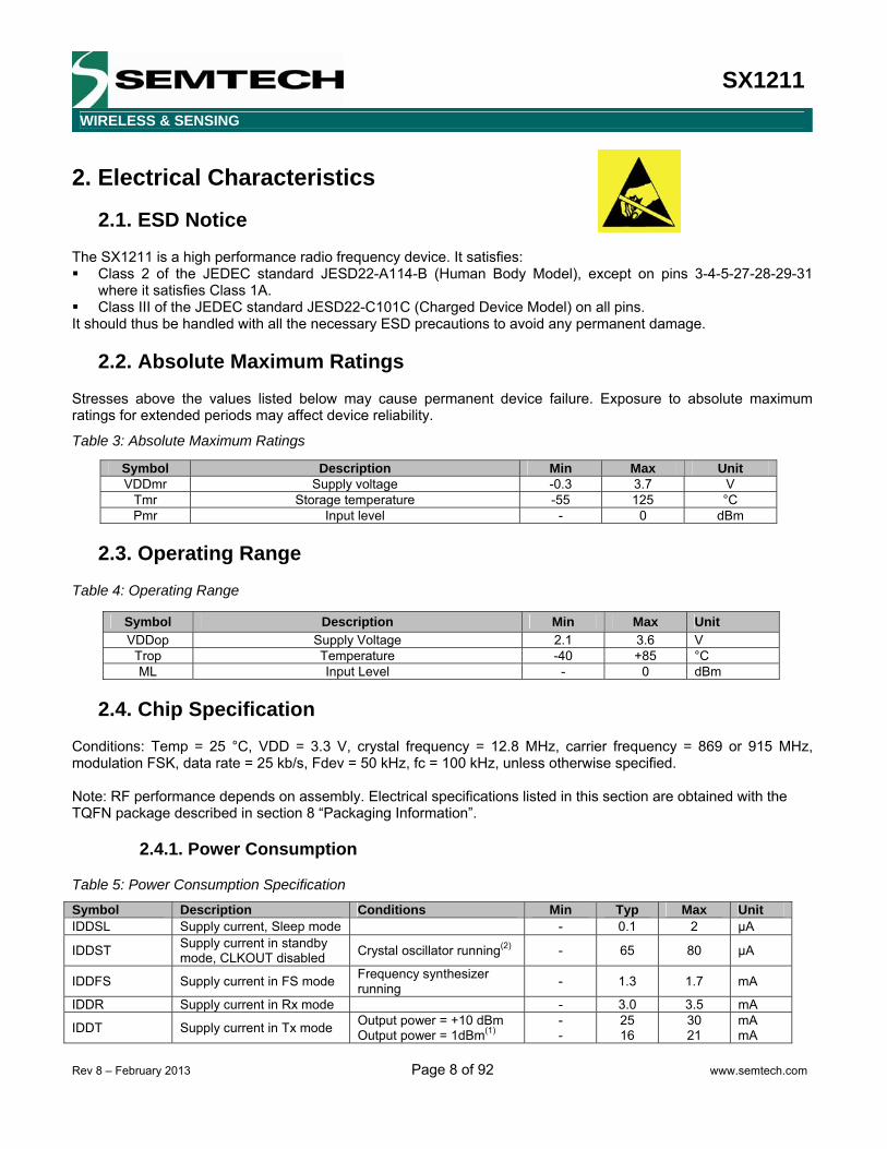
3.1. Power Supply Strategy To provide stable sensitivity and linearity characteristics over a wide supply range, the SX1211 is internally regulated. This internal regulated power supply structure is described below:
SX1211
WIRELESS & SENSING
Rev 8 – February 2013 Page 13 of 92 www.semtech.com
VDD – Pin 26 2.1 – 3.6V
External Supply
Reg_top 1.4 V
Reg_dig 1.0 V
Reg_VCO 0.85 V
Reg_PA 1.80 V
VR_VCO Pin 3
VR_PA Pin 29
Biasing : -PA Driver -PA choke (ext)
Biasing : -VCO circuit -Ext. VCO tank
Biasing digital blocks
VR_DIG Pin 28
Biasing analog blocks
VR_1V Pin 27
Reg_ana 1.0 V
Biasing : -SPI -Config. Registers -POR
1ųF Y5V
1ųF Y5V
220nFX7R
100nFX7R
47nF X7R
Vbat
Figure 4: Power Supply Breakdown
To ensure correct operation of the regulator circuit, the decoupling capacitor connection shown in Figure 4 is required. These decoupling components are recommended for any design.
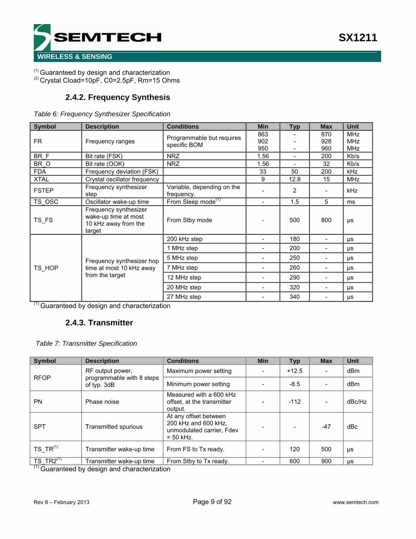
3.2. Frequency Synthesis Description The frequency synthesizer of the SX1211 is a fully integrated integer-N type PLL. The PLL circuit requires only five external components for the PLL loop filter and the VCO tank circuit.
3.2.1. Reference Oscillator
The SX1211 embeds a crystal oscillator, which provides the reference frequency for the PLL. The recommended crystal specification is given in section 7.1.
3.2.2. CLKOUT Output
The reference frequency, or a sub-multiple of it, can be provided on CLKOUT (pin 19) by activating the bit OSCParam_Clkout_on. The division ratio is programmed through bits OSCParam_Clkout_freq. The two applications of the CLKOUT output are: To provide a clock output for a companion uC, thus saving the cost of an additional oscillator. CLKOUT can be
made available in any operation mode, except Sleep mode, and is automatically enabled at power-up. To provide an oscillator reference output. Measurement of the CLKOUT signal enables simple software
trimming of the initial crystal tolerance. Note: To minimize the current consumption of the SX1211, ensure that the CLKOUT signal is disabled when unused.
SX1211
WIRELESS & SENSING
Rev 8 – February 2013 Page 14 of 92 www.semtech.com
3.2.3. PLL Architecture
The crystal oscillator (XO) forms the reference oscillator of an Integer-N Phase Locked Loop (PLL), whose operation is discussed in the following section. Figure 5 shows a block schematic of the SX1211 PLL. Here the crystal reference frequency and the software controlled dividers R, P and S determine the output frequency of the PLL.
PFD
÷75.(Pi+1)+Si
XO ÷(Ri+1)
VR_VCO
XT_M XT_P LF_M LF_P
VCO_M VCO_P
LO
VtuneFcomp
Figure 5: Frequency Synthesizer Description
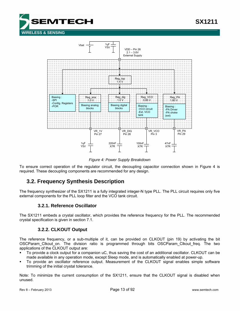
The VCO tank inductors are connected on an external differential input. Similarly, the loop filter is also located externally. However, there is an internal 8pF capacitance at VCO input that should be subtracted from the desired loop filter capacitance. The output signal of the VCO is used as the input to the local oscillator (LO) generator stage, illustrated in Figure 6. The VCO frequency is subdivided and used in a series of up (down) conversions for transmission (reception).
LO VCO Output
Receiver LOs
Transmitter LOs
LO1 Rx
LO2 Rx ÷8 90°
I
Q
LO1 Tx
90°
I
Q
LO2 Tx ÷8 90°
I
Q
Figure 6: LO Generator
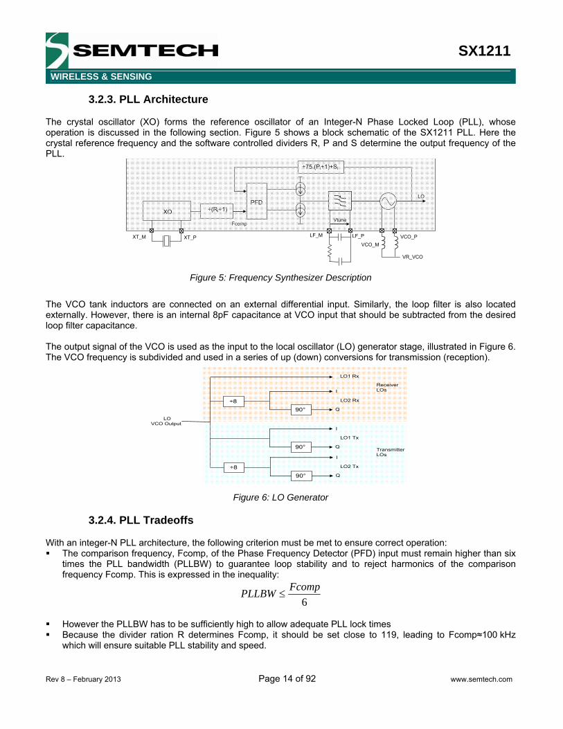
3.2.4. PLL Tradeoffs
With an integer-N PLL architecture, the following criterion must be met to ensure correct operation: The comparison frequency, Fcomp, of the Phase Frequency Detector (PFD) input must remain higher than six
times the PLL bandwidth (PLLBW) to guarantee loop stability and to reject harmonics of the comparison frequency Fcomp. This is expressed in the inequality:
6FcompPLLBW ≤
However the PLLBW has to be sufficiently high to allow adequate PLL lock times Because the divider ration R determines Fcomp, it should be set close to 119, leading to Fcomp≈100 kHz
which will ensure suitable PLL stability and speed.
SX1211
WIRELESS & SENSING
Rev 8 – February 2013 Page 15 of 92 www.semtech.com
With the recommended Bill Of Materials (BOM) of the reference design of section 7.5.3, the PLL prototype is the following: 64 ≤ R ≤ 169 S < P+1 PLLBW = 15 kHz nominal Startup times and reference frequency spurs as specified.
3.2.5. Voltage Controlled Oscillator
The integrated VCO requires only two external tank circuit inductors. As the input is differential, the two inductors should have the same nominal value. The performance of these components is important for both the phase noise and the power consumption of the PLL. It is recommended that a pair of high Q factor inductors is selected. These should be mounted orthogonally to other inductors (in particular the PA choke) to reduce spurious coupling between the PA and VCO. In addition, such measures may reduce radiated pulling effects and undesirable transient behavior, thus minimizing spectral occupancy. Note that ensuring a symmetrical layout of the VCO inductors will further improve PLL spectral purity. For best performance wound type inductors, with tight tolerance, should be used as described in section 7.5.3.
3.2.5.1. SW Settings of the VCO
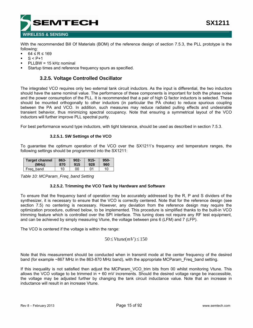
To guarantee the optimum operation of the VCO over the SX1211’s frequency and temperature ranges, the following settings should be programmed into the SX1211:
Target channel (MHz)
863-870
902-915
915-928
950-960
Freq_band 10 00 01 10
Table 10: MCParam_Freq_band Setting
3.2.5.2. Trimming the VCO Tank by Hardware and Software
To ensure that the frequency band of operation may be accurately addressed by the R, P and S dividers of the synthesizer, it is necessary to ensure that the VCO is correctly centered. Note that for the reference design (see section 7.5) no centering is necessary. However, any deviation from the reference design may require the optimization procedure, outlined below, to be implemented. This procedure is simplified thanks to the built-in VCO trimming feature which is controlled over the SPI interface. This tuning does not require any RF test equipment, and can be achieved by simply measuring Vtune, the voltage between pins 6 (LFM) and 7 (LFP). The VCO is centered if the voltage is within the range:
150)(50 ≤≤ mVVtune
Note that this measurement should be conducted when in transmit mode at the center frequency of the desired band (for example ~867 MHz in the 863-870 MHz band), with the appropriate MCParam_Freq_band setting. If this inequality is not satisfied then adjust the MCParam_VCO_trim bits from 00 whilst monitoring Vtune. This allows the VCO voltage to be trimmed in + 60 mV increments. Should the desired voltage range be inaccessible, the voltage may be adjusted further by changing the tank circuit inductance value. Note that an increase in inductance will result in an increase Vtune.
SX1211
WIRELESS & SENSING
Rev 8 – February 2013 Page 16 of 92 www.semtech.com
Note for mass production: The VCO capacitance is piece to piece dependant. As such, the optimization proposed above should be verified on several prototypes, to ensure that the population is centered on 100 mV.
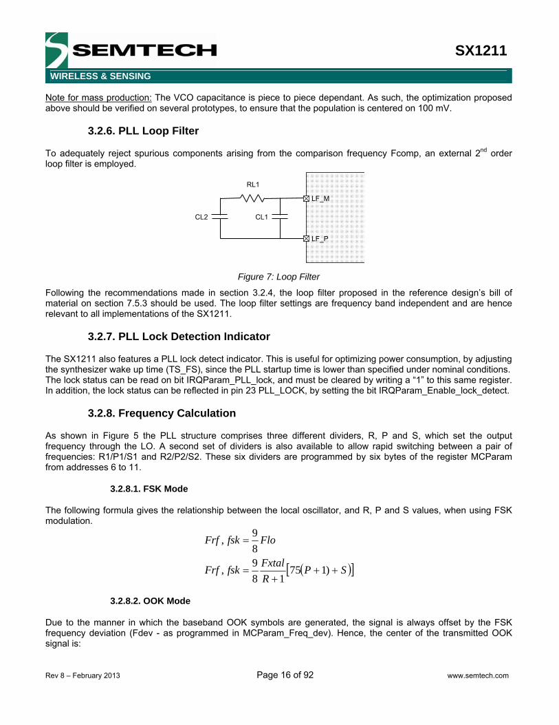
3.2.6. PLL Loop Filter
To adequately reject spurious components arising from the comparison frequency Fcomp, an external 2nd order loop filter is employed.
LF_M
CL1 CL2
LF_P
RL1
Figure 7: Loop Filter
Following the recommendations made in section 3.2.4, the loop filter proposed in the reference design’s bill of material on section 7.5.3 should be used. The loop filter settings are frequency band independent and are hence relevant to all implementations of the SX1211.
3.2.7. PLL Lock Detection Indicator
The SX1211 also features a PLL lock detect indicator. This is useful for optimizing power consumption, by adjusting the synthesizer wake up time (TS_FS), since the PLL startup time is lower than specified under nominal conditions. The lock status can be read on bit IRQParam_PLL_lock, and must be cleared by writing a “1” to this same register. In addition, the lock status can be reflected in pin 23 PLL_LOCK, by setting the bit IRQParam_Enable_lock_detect.
3.2.8. Frequency Calculation
As shown in Figure 5 the PLL structure comprises three different dividers, R, P and S, which set the output frequency through the LO. A second set of dividers is also available to allow rapid switching between a pair of frequencies: R1/P1/S1 and R2/P2/S2. These six dividers are programmed by six bytes of the register MCParam from addresses 6 to 11.
3.2.8.1. FSK Mode
The following formula gives the relationship between the local oscillator, and R, P and S values, when using FSK modulation.
( )[ ]SPRFxtalfskFrf
FlofskFrf
+++
=
=
)17518
9,
89,
3.2.8.2. OOK Mode
Due to the manner in which the baseband OOK symbols are generated, the signal is always offset by the FSK frequency deviation (Fdev - as programmed in MCParam_Freq_dev). Hence, the center of the transmitted OOK signal is:

SX1211
WIRELESS & SENSING
Rev 8 – February 2013 Page 17 of 92 www.semtech.com
( )[ ] FdevSPRFxtaltxookFrf
FdevFlotxookFrf
−+++
=
−=
)17518
9,,
89,,
Consequently, in receive mode, due to the low intermediate frequency (Low-IF) architecture of the SX1211 the frequency should be configured so as to ensure the correct low-IF receiver baseband center frequency, IF2.
( )[ ] 2)17518
9,,
289,,
IFSPRFxtalrxookFrf
IFFlorxookFrf
−+++
=
−=
Note that from Section 3.4.4, it is recommended that IF2 be set to 100 kHz.
SX1211
WIRELESS & SENSING
Rev 8 – February 2013 Page 18 of 92 www.semtech.com
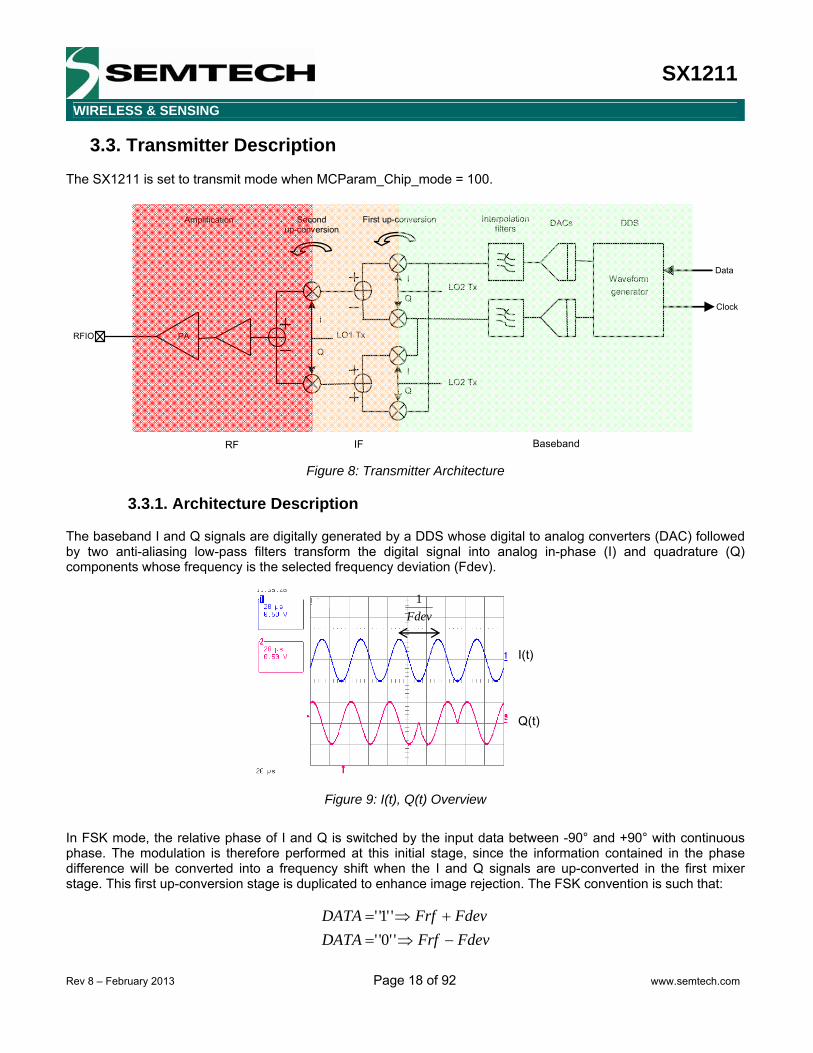
3.3. Transmitter Description The SX1211 is set to transmit mode when MCParam_Chip_mode = 100.
Waveform generator
LO1 Tx
LO2 Tx
LO2 Tx
RFIO PA
I
Q
Q
I
I
Q
DDS DACs Interpolation filters
Baseband IF RF
Data
Clock
First up-conversionSecond up-conversion
Amplification
Figure 8: Transmitter Architecture
3.3.1. Architecture Description
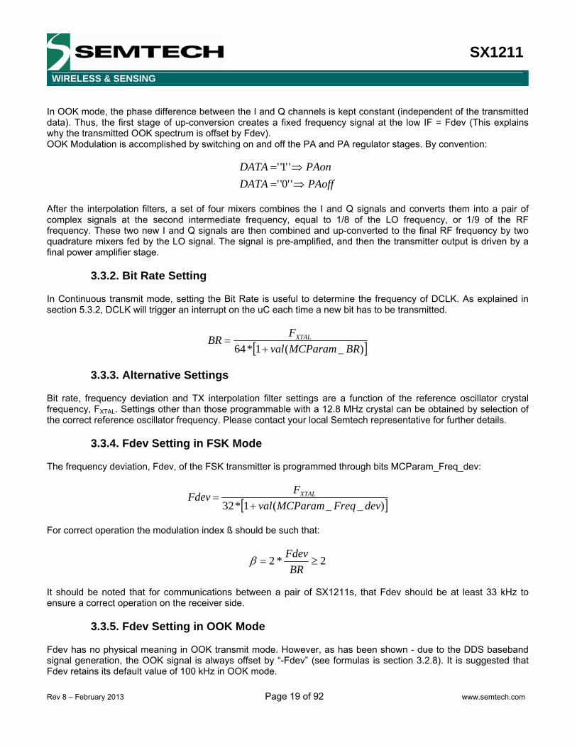
The baseband I and Q signals are digitally generated by a DDS whose digital to analog converters (DAC) followed by two anti-aliasing low-pass filters transform the digital signal into analog in-phase (I) and quadrature (Q) components whose frequency is the selected frequency deviation (Fdev).
I(t)
Q(t)
Fdev1
Figure 9: I(t), Q(t) Overview
In FSK mode, the relative phase of I and Q is switched by the input data between -90° and +90° with continuous phase. The modulation is therefore performed at this initial stage, since the information contained in the phase difference will be converted into a frequency shift when the I and Q signals are up-converted in the first mixer stage. This first up-conversion stage is duplicated to enhance image rejection. The FSK convention is such that:
FdevFrfDATAFdevFrfDATA
−⇒=+⇒=
''0''''1''
SX1211
WIRELESS & SENSING
Rev 8 – February 2013 Page 19 of 92 www.semtech.com
In OOK mode, the phase difference between the I and Q channels is kept constant (independent of the transmitted data). Thus, the first stage of up-conversion creates a fixed frequency signal at the low IF = Fdev (This explains why the transmitted OOK spectrum is offset by Fdev). OOK Modulation is accomplished by switching on and off the PA and PA regulator stages. By convention:
PAoffDATAPAonDATA
⇒=⇒=''0''''1''
After the interpolation filters, a set of four mixers combines the I and Q signals and converts them into a pair of complex signals at the second intermediate frequency, equal to 1/8 of the LO frequency, or 1/9 of the RF frequency. These two new I and Q signals are then combined and up-converted to the final RF frequency by two quadrature mixers fed by the LO signal. The signal is pre-amplified, and then the transmitter output is driven by a final power amplifier stage.
3.3.2. Bit Rate Setting
In Continuous transmit mode, setting the Bit Rate is useful to determine the frequency of DCLK. As explained in section 5.3.2, DCLK will trigger an interrupt on the uC each time a new bit has to be transmitted.
[ ])_(1*64 BRMCParamvalFBR XTAL
+=
3.3.3. Alternative Settings
Bit rate, frequency deviation and TX interpolation filter settings are a function of the reference oscillator crystal frequency, FXTAL. Settings other than those programmable with a 12.8 MHz crystal can be obtained by selection of the correct reference oscillator frequency. Please contact your local Semtech representative for further details.
3.3.4. Fdev Setting in FSK Mode
The frequency deviation, Fdev, of the FSK transmitter is programmed through bits MCParam_Freq_dev:
[ ])__(1*32 devFreqMCParamvalFFdev XTAL
+=
For correct operation the modulation index ß should be such that:
2*2 ≥=BR
Fdevβ
It should be noted that for communications between a pair of SX1211s, that Fdev should be at least 33 kHz to ensure a correct operation on the receiver side.
3.3.5. Fdev Setting in OOK Mode
Fdev has no physical meaning in OOK transmit mode. However, as has been shown - due to the DDS baseband signal generation, the OOK signal is always offset by “-Fdev” (see formulas is section 3.2.8). It is suggested that Fdev retains its default value of 100 kHz in OOK mode.
SX1211
WIRELESS & SENSING
Rev 8 – February 2013 Page 20 of 92 www.semtech.com
3.3.6. Interpolation Filter
After digital to analog conversion, both I and Q signals are smoothed by interpolation filters. This block low-pass filters the digitally generated signal, and prevents the alias signals from entering the modulators. Its bandwidth can be programmed with the register RXParam_InterpFiltTx, and should be set to:
⎥⎦⎤
⎢⎣⎡ +≅
2*3 BRFdevBW
Where Fdev is the programmed frequency deviation as set in MCParam_Freq_dev, and BR is the physical Bit Rate of transmission. Notes: Low interpolation filter bandwidth will attenuate the baseband I/Q signals thus reducing the power of the FSK
signal. Conversely, excessive bandwidth will degrade spectral purity. For the wideband FSK modulation, for example when operating in DTS mode, the recommended filter setting
can not be reached. However, the impact upon spectral purity will be negligible, due to the already wideband channel.
3.3.7. Power Amplifier
The Power Amplifier (PA) integrated in the SX1211 operates under a regulated voltage supply of 1.8 V. The external PA choke inductor is biased by an internal regulator output made available on pin 29 (VR_PA). Thanks to these features, the PA output power is consistent over the power supply range. This is important for mobile applications where this allows both predictable RF performance and battery life.
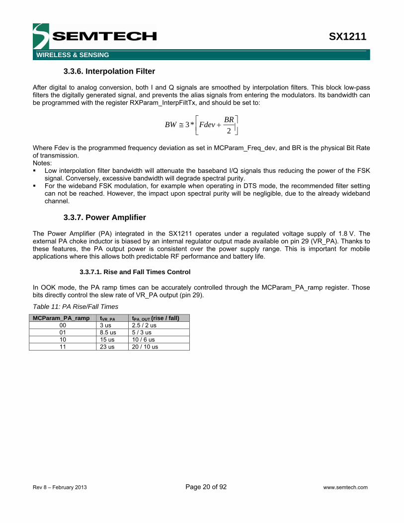
3.3.7.1. Rise and Fall Times Control
In OOK mode, the PA ramp times can be accurately controlled through the MCParam_PA_ramp register. Those bits directly control the slew rate of VR_PA output (pin 29).
Table 11: PA Rise/Fall Times
MCParam_PA_ramp tVR_PA tPA_OUT (rise / fall)00 3 us 2.5 / 2 us 01 8.5 us 5 / 3 us 10 15 us 10 / 6 us 11 23 us 20 / 10 us
SX1211
WIRELESS & SENSING
Rev 8 – February 2013 Page 21 of 92 www.semtech.com
DATA
VR_PA [V] 95 %
tVR_PA tVR_PA
95 %
60 dB 60 dB PA Output power
tPA_OUT tPA_OUT
Figure 10: PA Control
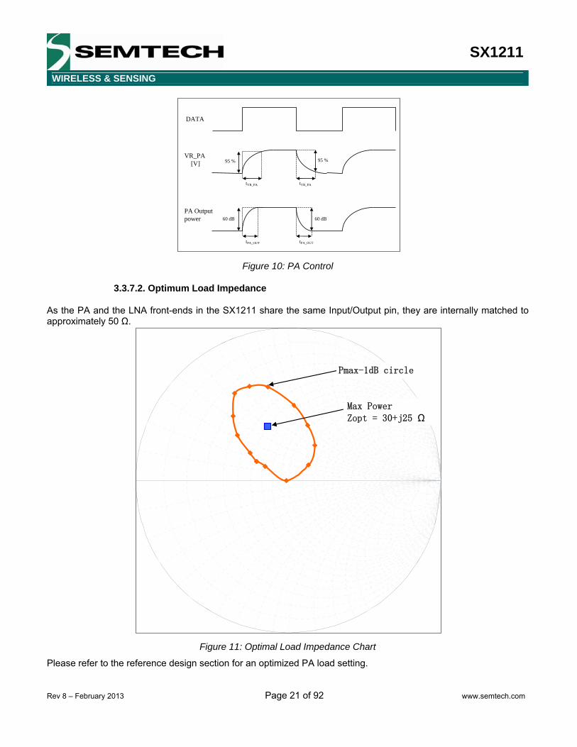
3.3.7.2. Optimum Load Impedance
As the PA and the LNA front-ends in the SX1211 share the same Input/Output pin, they are internally matched to approximately 50 Ω.
Pmax-1dB circle
Max PowerZopt = 30+j25 Ω
Figure 11: Optimal Load Impedance Chart
Please refer to the reference design section for an optimized PA load setting.

SX1211
WIRELESS & SENSING
Rev 8 – February 2013 Page 22 of 92 www.semtech.com
3.3.7.3. Suggested PA Biasing and Matching
The recommended PA bias and matching circuit is illustrated below:
Figure 12: Recommended PA Biasing and Output Matching
Please refer to section 7.5.3 of this document for the optimized matching arrangement for each frequency band.
3.3.8. Common Input and Output Front-End
The receiver and the transmitter share the same RFIO pin (pin 31). Figure 13 below shows the configuration of the common RF front-end. In transmit mode, the PA and the PA regulator are active, with the voltage on the VR_PA pin equal to the
nominal voltage of the regulator (1.8 V). The external inductance is used to bias the PA. In receive mode, both PA and PA regulator are off and VR_PA is tied to ground. The external inductance LT1
is then used to bias the LNA.
RFIO
VR_PA
PA
Reg_PA
Rx_on
LNA
To Antenna
Figure 13: Front-end Description
VR_PA
RFIO
100nH
47nF
SAW
Low-pass and DC block
PA
Antenna port
DC block

SX1211
WIRELESS & SENSING
Rev 8 – February 2013 Page 23 of 92 www.semtech.com
3.4. Receiver Description The SX1211 is set to receive mode when MCParam_Chip_mode = 011.
FSKdemod
Bit synchronizer
OOKdemod
Control logic -Pattern recognition -FIFO handler -SPI interface -Packet handler
RSSI
LO1 Rx
LO2 Rx LNA
Baseband, IF2 in OOK IF1 RF
First down-conversion
Second down-conversion
Figure 14: Receiver Architecture
3.4.1. Architecture
The SX1211 receiver employs a super-heterodyne architecture. Here, the first IF is 1/9th of the RF frequency (approximately 100MHz). The second down-conversion down-converts the I and Q signals to base band in the case of the FSK receiver (Zero IF) and to a low-IF (IF2) for the OOK receiver.
Channel LO1 Rx Image frequencyIF1
≈100MHz
First down-conversionSecond
down-conversion
0
IF2=0 in FSK mode
Frequencyl
LO2 Rx
Figure 15: FSK Receiver Setting
Channel LO1 Rx Image frequencyIF1
≈100MHz
First down-conversionSecond
down-conversion
0 IF2<0 in FSK mode
equal to fo
LO2 Rx Frequency
Figure 16: OOK Receiver Setting
After the second down-conversion stage, the received signal is channel-select filtered and amplified to a level adequate for demodulation. Both FSK and OOK demodulation are available. Finally, an optional Bit Synchronizer (BitSync) is provided, to be supply a synchronous clock and data stream to a companion uC in Continuous mode,
SX1211
WIRELESS & SENSING
Rev 8 – February 2013 Page 24 of 92 www.semtech.com
or to fill the FIFO buffers with glitch-free data in Buffered mode. The operation of the receiver is now described in detail. Note: Image rejection is achieved by the SAW filter.
3.4.2. LNA and First Mixer
In receive mode, the RFIO pin is connected to a fixed gain, common-gate, Low Noise Amplifier (LNA). The performance of this amplifier is such that the Noise Figure (NF) of the receiver can be estimated to be ≈7 dB.
3.4.3. IF Gain and Second I/Q Mixer
Following the LNA and first down-conversion, there is an IF amplifier whose gain can be programmed from -13.5 dB to 0 dB in 4.5 dB steps, via the register MCParam_IF_gain. The default setting corresponds to 0 dB gain, but lower values can be used to increase the RSSI dynamic range. Refer to section 3.4.7 for additional information.
3.4.4. Channel Filters
The second mixer stages are followed by the channel select filters. The channel select filters have a strong influence on the noise bandwidth and selectivity of the receiver and hence its sensitivity. Each filter comprises a passive and active section.
3.4.4.1. Passive Filter
Each channel select filter features a passive second-order RC filter, with a bandwidth programmable through the bits RXParam_PassiveFilt. As the wider of the two filters, its effect on the sensitivity is negligible, but its bandwidth has to be setup instead to optimize blocking immunity. The value entered into this register sets the single side bandwidth of this filter. For optimum performance it should be set to 3 to 4 times the cutoff frequency of the active Butterworth (or polyphase) filter described in the next section.
ButterFiltfilterpassivetButterfFil FcBWFc *4*3 , ≤≤
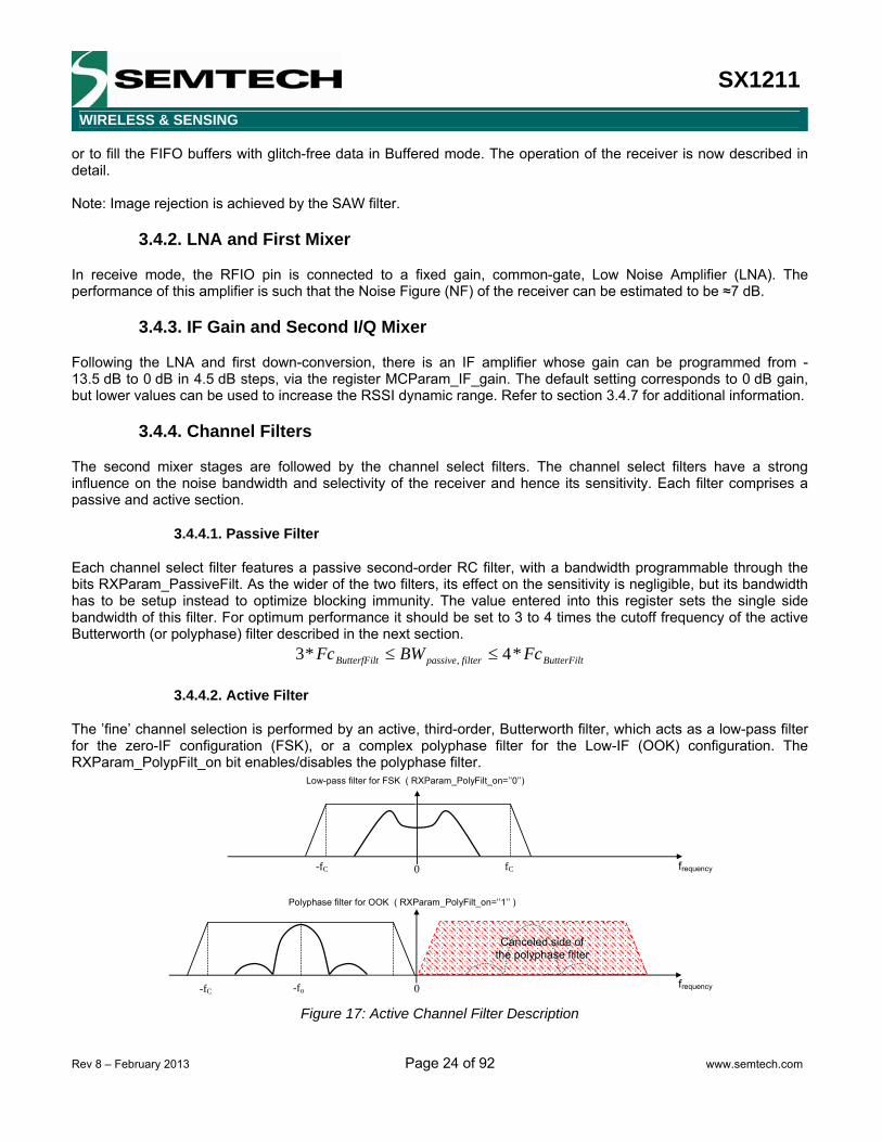
3.4.4.2. Active Filter
The ’fine’ channel selection is performed by an active, third-order, Butterworth filter, which acts as a low-pass filter for the zero-IF configuration (FSK), or a complex polyphase filter for the Low-IF (OOK) configuration. The RXParam_PolypFilt_on bit enables/disables the polyphase filter.
fC
Low-pass filter for FSK ( RXParam_PolyFilt_on=’’0’’)
Polyphase filter for OOK ( RXParam_PolyFilt_on=’’1’’ )
-fC 0 frequency
frequency0 -fC -fo
Canceled side of the polyphase filter
Figure 17: Active Channel Filter Description
SX1211
WIRELESS & SENSING
Rev 8 – February 2013 Page 25 of 92 www.semtech.com
As can be seen from Figure 17, the required bandwidth of this filter varies between the two demodulation modes. FSK mode: The 99% energy bandwidth of an FSK modulated signal is approximated to be:
⎥⎦⎤
⎢⎣⎡ +=
2*2%,99
BRFdevBW FSK
The bits RXParam_ButterFilt set fc, the cutoff frequency of the filter. As we are in a Zero-IF configuration, the FSK lobes are centered around the virtual “DC” frequency. The choice of fc should be such that the modulated signal falls in the filter bandwidth, anticipating the Local Oscillator frequency drift over the operating temperature and aging of the device:
driftsFSK LOBWfc +> %,99*2
Please refer to the charts in section 3.4.5 for an accurate overview of the filter bandwidth vs. setting. OOK mode: The 99% energy bandwidth of an OOK modulated signal is approximated to be:
BRTbit
BW OOK .22%,99 ==
The bits RXParam_PolypFilt_center set fo, the center frequency of the polyphase filter when activated. fo should always be chosen to be equal to the low Intermediate Frequency of the receiver (IF2). This is why, in the GUI described in section 7.2.1 of this document, the low IF frequency of the OOK receiver denoted IF2 has been replaced by fo. The following setting is recommended:
"0011"_100
==
PolypFiltRXParamkHzfo
The value stored in RXParam_ButterFilt determines fc, the filter cut-off frequency. So the user should set fc according to:
driftsOOK LOBWfofc +>− %,99)(*2
Again, fc as a function of RXParam_ButterFilt is given in the section 3.4.6.
3.4.5. Channel Filters Setting in FSK Mode
Fc, the 3dB cutoff frequency of the Butterworth filter used in FSK reception, is programmed through the bit RXParam_ButterFilt. However, the whole receiver chain influences this cutoff frequency. Thus the channel select and resultant filter bandwidths are summarized in the following chart:

SX1211
WIRELESS & SENSING
Rev 8 – February 2013 Page 26 of 92 www.semtech.com
Butterworth Filter's BW, FSK
0
50
100
150
200
250
300
350
400
450
0 2 4 6 8 10 12 14 16
Val (RXParam_ButterFilt) [d]
Fc (3
dB C
utof
f) [k
Hz]
ActualBW
TheoreticalBW
Figure 18: Butterworth Filter's Actual BW
Table 37 suggests filter settings in FSK mode, along with the corresponding passive filter bandwidth and the accepted tolerance on the crystal reference.
3.4.6. Channel Filters Setting in OOK Mode
The center frequency, fo, is always set to 100kHz. The following chart shows the receiver bandwidth when changing RXParam_Butterfilt bits, whilst the polyphase filter is activated.
Polyphase Filter's BW, OOK
0
50
100
150
200
250
300
350
400
450
0 2 4 6 8 10 12 14 16Val (RXParam_ButterFilt [d]RXParam_PolypFilt="0011"
Fc-F
o w
ith F
o=10
0 kH
z [k
Hz]
ActualBW
TheoreticalBW
Figure 19: Polyphase Filter's Actual BW
Table 38 suggests a few filter settings in OOK mode, along with the corresponding passive filter bandwidth and the accepted tolerance on the crystal reference.
3.4.7. RSSI
After filtering, the In-phase and Quadrature signals are amplified by a chain of 11 amplifiers, each with 6dB gain. The outputs of these amplifiers are used to evaluate the Received Signal Strength (RSSI).
3.4.7.1. Resolution and Accuracy
Whilst the RSSI resolution is 0.5 dB, the absolute accuracy is not expected to be better than +/- 3dB due to process and external component variation. Higher accuracy whilst performing absolute RSSI measurements will require additional calibration.
3.4.7.2. Acquisition Time
SX1211
WIRELESS & SENSING
Rev 8 – February 2013 Page 27 of 92 www.semtech.com
In OOK mode, the RSSI evaluates the signal strength by sampling I(t) and Q(t) signals 16 times in each period of the chosen IF2 frequency (refer to section 3.4.1). In FSK mode, the signals are sampled 16 times in each Fdev period, Fdev being the frequency deviation of the companion transmitter. An average is then performed over a sliding window of 16 samples. Hence, the RSSI output register RXParam_RSSI is updated 16 times in each Fdev or IF2 period. The following settings should be respected: FSK Mode: Ensure that the Fdev parameter (as described in MCParam_Fdev) remains consistent with the
actual frequency deviation of the companion transmitter. OOK reception: Ensure that the Fdev parameter (as described in MCParam_Fdev) is equal with the frequency
of I(t) and Q(t) signals, i.e. the second Intermediate Frequency, IF2, of the receiver (Note that this equals Fo, the center frequency of the polyphase filter).
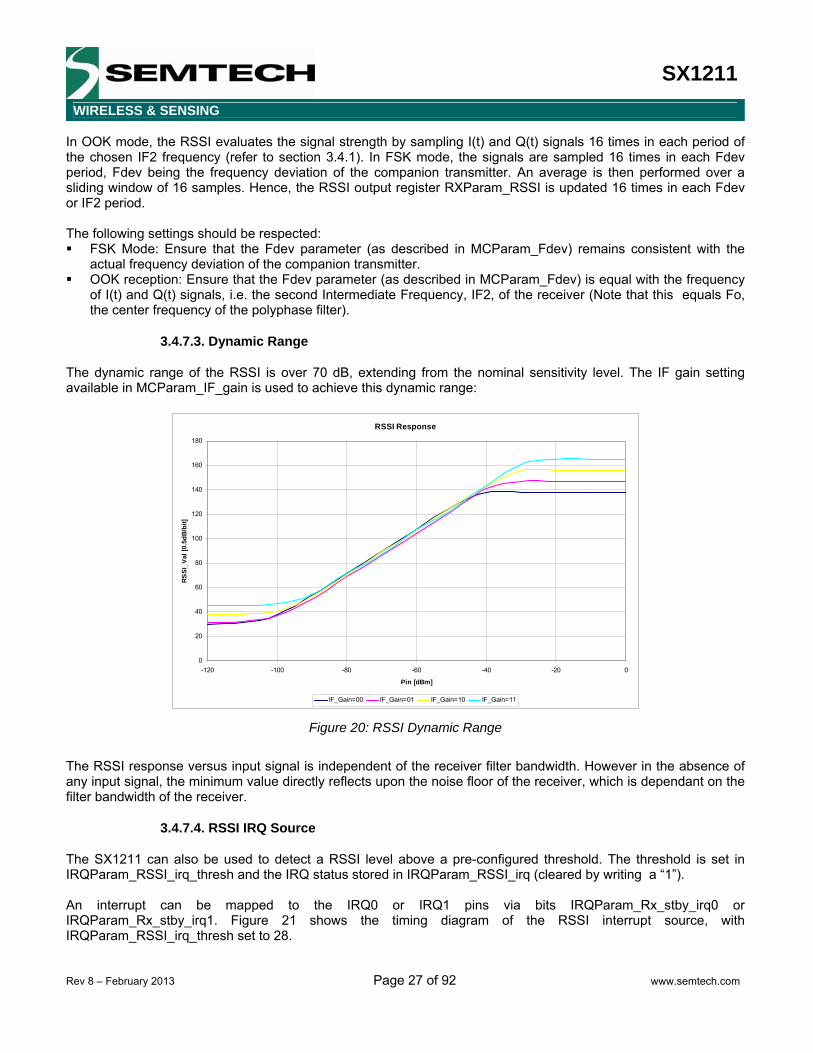
3.4.7.3. Dynamic Range
The dynamic range of the RSSI is over 70 dB, extending from the nominal sensitivity level. The IF gain setting available in MCParam_IF_gain is used to achieve this dynamic range:
RSSI Response
0
20
40
60
80
100
120
140
160
180
-120 -100 -80 -60 -40 -20 0
Pin [dBm]
RSS
I_V
al [0
.5dB
/bit]
IF_Gain=00 IF_Gain=01 IF_Gain=10 IF_Gain=11
Figure 20: RSSI Dynamic Range
The RSSI response versus input signal is independent of the receiver filter bandwidth. However in the absence of any input signal, the minimum value directly reflects upon the noise floor of the receiver, which is dependant on the filter bandwidth of the receiver.
3.4.7.4. RSSI IRQ Source
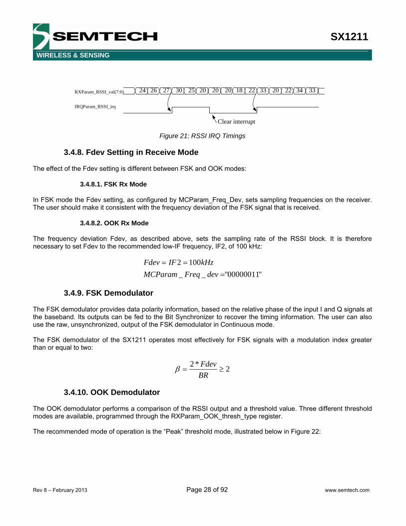
The SX1211 can also be used to detect a RSSI level above a pre-configured threshold. The threshold is set in IRQParam_RSSI_irq_thresh and the IRQ status stored in IRQParam_RSSI_irq (cleared by writing a “1”). An interrupt can be mapped to the IRQ0 or IRQ1 pins via bits IRQParam_Rx_stby_irq0 or IRQParam_Rx_stby_irq1. Figure 21 shows the timing diagram of the RSSI interrupt source, with IRQParam_RSSI_irq_thresh set to 28.
SX1211
WIRELESS & SENSING
Rev 8 – February 2013 Page 28 of 92 www.semtech.com
IRQParam_RSSI_irq
Clear interrupt
24 26 27 30 25 20 20 20 18 22 20 22 34 33 33 RXParam_RSSI_val(7:0)
Figure 21: RSSI IRQ Timings
3.4.8. Fdev Setting in Receive Mode
The effect of the Fdev setting is different between FSK and OOK modes:
3.4.8.1. FSK Rx Mode
In FSK mode the Fdev setting, as configured by MCParam_Freq_Dev, sets sampling frequencies on the receiver. The user should make it consistent with the frequency deviation of the FSK signal that is received.
3.4.8.2. OOK Rx Mode
The frequency deviation Fdev, as described above, sets the sampling rate of the RSSI block. It is therefore necessary to set Fdev to the recommended low-IF frequency, IF2, of 100 kHz:
"00000011"__1002
===
devFreqMCParamkHzIFFdev
3.4.9. FSK Demodulator
The FSK demodulator provides data polarity information, based on the relative phase of the input I and Q signals at the baseband. Its outputs can be fed to the Bit Synchronizer to recover the timing information. The user can also use the raw, unsynchronized, output of the FSK demodulator in Continuous mode. The FSK demodulator of the SX1211 operates most effectively for FSK signals with a modulation index greater than or equal to two:
2*2≥=
BRFdevβ
3.4.10. OOK Demodulator
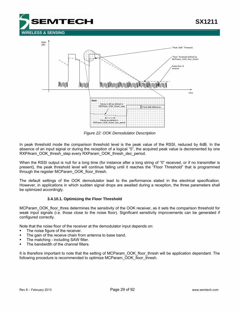
The OOK demodulator performs a comparison of the RSSI output and a threshold value. Three different threshold modes are available, programmed through the RXParam_OOK_thresh_type register. The recommended mode of operation is the “Peak” threshold mode, illustrated below in Figure 22:
SX1211
WIRELESS & SENSING
Rev 8 – February 2013 Page 29 of 92 www.semtech.com
Zoom
Period as defined in RXParam_OOK_thresh_dec_period
Decay in dB as defined in RXPAram_OOK_thresh_step Fixed 6dB difference
RSSI (dB)
Noise floor of receiver
‘’Floor’’ threshold defined by MCParam_OOK_floor_thresh
Time
‘’Peak -6dB’’ Threshold
Zoom
Figure 22: OOK Demodulator Description
In peak threshold mode the comparison threshold level is the peak value of the RSSI, reduced by 6dB. In the absence of an input signal or during the reception of a logical “0”, the acquired peak value is decremented by one RXPAram_OOK_thresh_step every RXParam_OOK_thresh_dec_period. When the RSSI output is null for a long time (for instance after a long string of “0” received, or if no transmitter is present), the peak threshold level will continue falling until it reaches the “Floor Threshold” that is programmed through the register MCParam_OOK_floor_thresh. The default settings of the OOK demodulator lead to the performance stated in the electrical specification. However, in applications in which sudden signal drops are awaited during a reception, the three parameters shall be optimized accordingly.
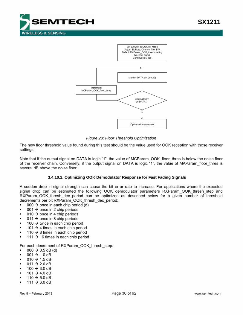
3.4.10.1. Optimizing the Floor Threshold
MCParam_OOK_floor_thres determines the sensitivity of the OOK receiver, as it sets the comparison threshold for weak input signals (i.e. those close to the noise floor). Significant sensitivity improvements can be generated if configured correctly. Note that the noise floor of the receiver at the demodulator input depends on: The noise figure of the receiver. The gain of the receive chain from antenna to base band. The matching - including SAW filter. The bandwidth of the channel filters.
It is therefore important to note that the setting of MCParam_OOK_floor_thresh will be application dependant. The following procedure is recommended to optimize MCParam_OOK_floor_thresh.
SX1211
WIRELESS & SENSING
Rev 8 – February 2013 Page 30 of 92 www.semtech.com
Set SX1211 in OOK Rx mode Adjust Bit Rate, Channel filter BW
Default RXParam_OOK_thresh setting No input signal
Continuous Mode
Optimization complete
Glitch activity on DATA ?
Monitor DATA pin (pin 20)
Increment MCParam_OOK_floor_thres
Figure 23: Floor Threshold Optimization
The new floor threshold value found during this test should be the value used for OOK reception with those receiver settings. Note that if the output signal on DATA is logic “1”, the value of MCParam_OOK_floor_thres is below the noise floor of the receiver chain. Conversely, if the output signal on DATA is logic “1”, the value of MAParam_floor_thres is several dB above the noise floor.
3.4.10.2. Optimizing OOK Demodulator Response for Fast Fading Signals
A sudden drop in signal strength can cause the bit error rate to increase. For applications where the expected signal drop can be estimated the following OOK demodulator parameters RXParam_OOK_thresh_step and RXParam_OOK_thresh_dec_period can be optimized as described below for a given number of threshold decrements per bit RXParam_OOK_thresh_dec_period: 000 once in each chip period (d) 001 once in 2 chip periods 010 once in 4 chip periods 011 once in 8 chip periods 100 twice in each chip period 101 4 times in each chip period 110 8 times in each chip period 111 16 times in each chip period
For each decrement of RXParam_OOK_thresh_step: 000 0.5 dB (d) 001 1.0 dB 010 1.5 dB 011 2.0 dB 100 3.0 dB 101 4.0 dB 110 5.0 dB 111 6.0 dB

SX1211
WIRELESS & SENSING
Rev 8 – February 2013 Page 31 of 92 www.semtech.com
3.4.10.3. Alternative OOK Demodulator Threshold Modes
In addition to the Peak OOK threshold mode, the user can alternatively select two other types of threshold detectors: Fixed threshold: The value is selected through the MCParam_OOK_floor_thresh register (refer to section
3.4.10.1 for further information concerning optimization of the floor threshold). Average threshold: Data supplied by the RSSI block is averaged with the following cutoff frequency:
π*800__ BRFcutoffcutoffOOKRXParam =⇒=
π*3211__ BRFcutoffcutoffOOKRXParam =⇒=
In the first example, the higher cut-off frequency enables a sequence of up to 8 consecutive “0” or “1” to be supported, whilst the lower cut-off frequency presented in the second example allows for the correct reception of up to 32 consecutive “0” or “1”.
3.4.11. Bit Synchronizer
The Bit Synchronizer (BitSync) is a block that provides a clean and synchronized digital output, free of glitches.
Raw demodulator
output (FSK or OOK)
DCLK IRQ_1
DATA BitSync Output
To pin DATA and DCLK in continuous
mode
Figure 24: BitSync Description
The BitSync can be disabled through the bits RXParam_Bitsync_off, and by holding pin IRQ1 low. However, for optimum receiver performance, its use when running Continuous mode is strongly advised. With this option a DCLK signal is present on pin IRQ_1. The BitSync is automatically activated in Buffered and Packet modes. The bit synchronizer bit-rate is controlled by MCParam_BR. For a given bit rate, this parameter is determined by:
[ ]BRMCParamF
BR XTAL
_1*64 +=

SX1211
WIRELESS & SENSING
Rev 8 – February 2013 Page 32 of 92 www.semtech.com
To ensure correct operation of the Bit Synchronizer, the following conditions have to be satisfied: A preamble (0x55 or 0xAA) of three bytes is required for synchronization, the longer the synchronization the
better the packet success rate The subsequent payload bit stream must have at least one transition from '0' to '1' or '1' to'0 every 16 bits
during data transmission The bit rate matching between the transmitter and the receiver must be better than 6.5%.
3.4.12. Alternative Settings
Bit Synchronizer and Active channel filter settings are a function of the reference oscillator crystal frequency, FXTAL. Settings other than those programmable with a 12.8 MHz crystal can be obtained by selection of the correct reference oscillator frequency. Please contact your local Semtech representative for further details.
3.4.13. Data Output
After OOK or FSK demodulation, the baseband signal is made available to the user on pin 20, DATA, when Continuous mode is selected. In Buffered and Packet modes, the data is retrieved from the FIFO through the SPI interface.

SX1211
WIRELESS & SENSING
Rev 8 – February 2013 Page 33 of 92 www.semtech.com
4. Operating Modes This section summarizes the settings for each operating mode of the SX1211, and explains the functionality available and the timing requirements for switching between modes.
4.1. Modes of Operation Table 12: Operating Modes
Mode MCParam_Chip_mode Active blocksSleep 000 SPI, POR Standby 001 SPI, POR, Top regulator, digital regulator, XO, CLKOUT (if activated through
OSCParam_Clkout) FS 010 Same + VCO regulator, all PLL and LO generation blocks Receive 011 Same as FS mode + LNA, first mixer, IF amplifier, second mixer set, channel
filters, baseband amplifiers and limiters, RSSI, OOK or FSK demodulator, BitSync and all digital features if enabled
Transmit 100 Same as FS mode + DDS, Interpolation filters, all up-conversion mixers, PA driver, PA and external VR_PA pin output for PA choke.
4.2. Digital Pin Configuration vs. Chip Mode Table 13 describes the state of the digital IOs in each of the above described modes of operation, regardless of the data operating mode (Continuous, Buffered, or Packet).
Table 13: Pin Configuration vs. Chip Mode
Chip ……….Mode Pin
Sleep mode
Standby mode FS mode Receive
mode Transmit mode Comment
NSS_CONFIG Input Input Input Input Input NSS_CONFIG has the priority over NSS_DATA
NSS_DATA Input Input Input Input Input
MISO Input Input Input Input Input Output only if NSS_CONFIG or NSSDATA=’0’
MOSI Input Input Input Input Input SCK Input Input Input Input Input IRQ_0 High-Z Output (1) Output (1) Output Output IRQ_1 High-Z Output (1) Output (1) Output Output DATA Input Input Input Output Input CLKOUT High-Z Output Output Output Output PLL_LOCK High-Z Output (2) Output (2) Output (2) Output (2)
Notes: (1): High-Z if Continuous mode is activated, else Output (2): Output if PLL_lock_en = 1, else High-Z (3): Valid logic states must be applied to inputs at all times to avoid unwanted leakage currents
SX1211
WIRELESS & SENSING
Rev 8 – February 2013 Page 34 of 92 www.semtech.com
5. Data Processing
5.1. Overview
5.1.1. Block Diagram
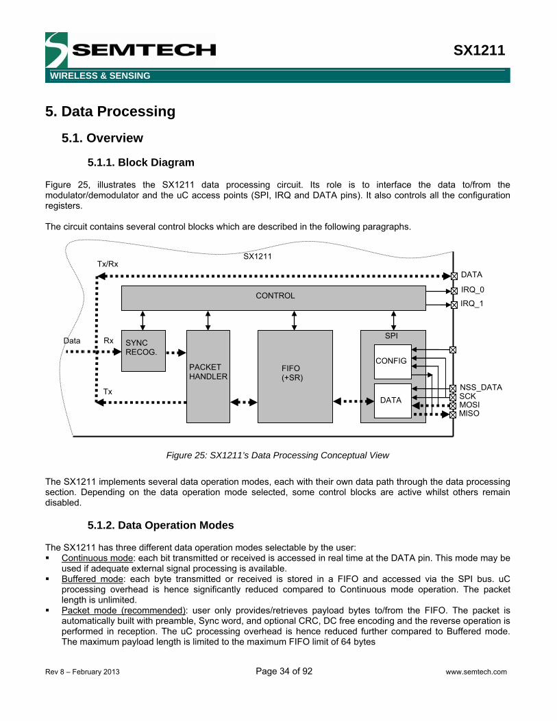
Figure 25, illustrates the SX1211 data processing circuit. Its role is to interface the data to/from the modulator/demodulator and the uC access points (SPI, IRQ and DATA pins). It also controls all the configuration registers. The circuit contains several control blocks which are described in the following paragraphs.
CONTROL
DATA
CONFIG
SPI
PACKET HANDLER
SYNC RECOG.
DATA
IRQ_0
IRQ_1
MISO MOSI SCK NSS_DATA
Rx
Tx
Tx/Rx
Data
SX1211
FIFO (+SR)
Figure 25: SX1211’s Data Processing Conceptual View
The SX1211 implements several data operation modes, each with their own data path through the data processing section. Depending on the data operation mode selected, some control blocks are active whilst others remain disabled.
5.1.2. Data Operation Modes
The SX1211 has three different data operation modes selectable by the user: Continuous mode: each bit transmitted or received is accessed in real time at the DATA pin. This mode may be
used if adequate external signal processing is available. Buffered mode: each byte transmitted or received is stored in a FIFO and accessed via the SPI bus. uC
processing overhead is hence significantly reduced compared to Continuous mode operation. The packet length is unlimited.
Packet mode (recommended): user only provides/retrieves payload bytes to/from the FIFO. The packet is automatically built with preamble, Sync word, and optional CRC, DC free encoding and the reverse operation is performed in reception. The uC processing overhead is hence reduced further compared to Buffered mode. The maximum payload length is limited to the maximum FIFO limit of 64 bytes

SX1211
WIRELESS & SENSING
Rev 8 – February 2013 Page 35 of 92 www.semtech.com
Table 14: Data Operation Mode Selection
MCParam_Data_mode Data Operation Mode 00 Continuous 01 Buffered 1x Packet
Each of these data operation modes is described fully in the following sections.
5.2. Control Block Description
5.2.1. SPI Interface
5.2.1.1. Overview
As illustrated in the Figure 26 below, the SX1211’s SPI interface consists of two sub blocks: SPI Config: used in all data operation modes to read and write the configuration registers which control all the
parameters of the chip (operating mode, bit rate, etc...) SPI Data: used in Buffered and Packet mode to write and read data bytes to and from the FIFO. (FIFO
interrupts can be used to manage the FIFO content.)
SPIDATA(slave)
MOSIMISOSCK
SPICONFIG(slave)
Config. Registers
SX1211
NSS_DATA
µ C(master)
NSS_CONFIGNSS_CONFIG MOSI MISO SCK NSS_DATA
Config. Registers
FIFO
Figure 26: SPI Interface Overview and uC Connections
Both interfaces are configured in slave mode whilst the uC is configured as the master. They have separate selection pins (NSS_CONFIG and NSS_DATA) but share the remaining pins: SCK (SPI Clock): clock signal provided by the uC MOSI (Master Out Slave In): data input signal provided by the uC MISO (Master In Slave Out): data output signal provided by the SX1211
As described below, only one interface can be selected at a time with NSS_CONFIG having the priority:

SX1211
WIRELESS & SENSING
Rev 8 – February 2013 Page 36 of 92 www.semtech.com
Table 15: Config vs. Data SPI Interface Selection
NSS_DATA NSS_CONFIG SPI Interface0 0 Config 0 1 Data 1 0 Config 1 1 None
The following paragraphs describe how to use each of these interfaces.
5.2.1.2. SPI Config
Write Register To write a value into a configuration register the timing diagram below should be carefully followed by the uC. The register’s new value is effective from the rising edge of NSS_CONFIG.
start A(4) A(3) A(2) A(1) D(7) D(6) D(5) D(4) D(3) D(2) D(1) D(0)
x x x x x x x D(7) D(6) D(5) D(4) D(3) D(2) D(1)
SCK (In)
MOSI (In)
MISO (Out)
NSS_CONFIG (In)
rw A(0)
Address = A1Current value at
address A1*
* when writing the new value at address A1, the current content of A1 can be read by the uC. (In)/(Out) refers to SX1211 side
New value at address A1
x HZ (input)
D(0)
stop
1 5 4 3 2 6 987 10 11 12 13 14 15 16
HZ (input)
Figure 27: Write Register Sequence
Note that when writing more than one register successively, it is not compulsory to toggle NSS_CONFIG back high between two write sequences. The bytes are alternatively considered as address and value. In this instance, all new values will become effective on rising edge of NSS_CONFIG. Read Register
To read the value of a configuration register the timing diagram below should be carefully followed by the uC.
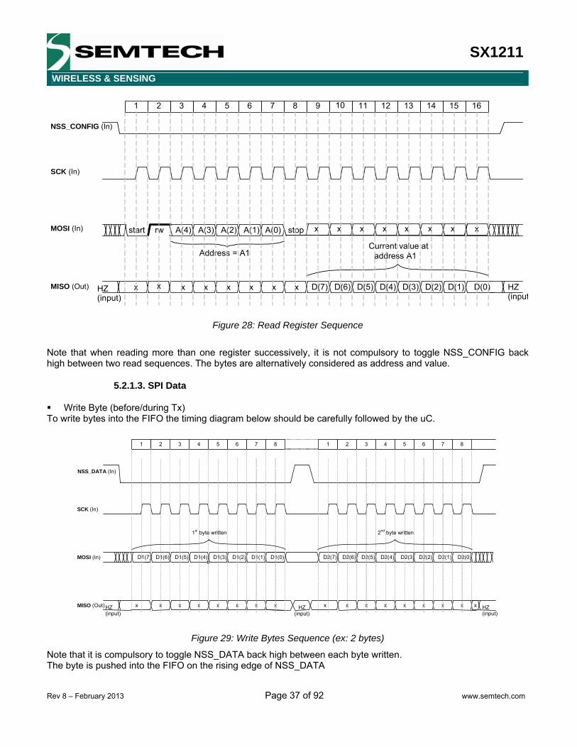
SX1211
WIRELESS & SENSING
Rev 8 – February 2013 Page 37 of 92 www.semtech.com
start A(4) A(3) A(2) A(1)
x x x x x x x D(7) D(6) D(5) D(4) D(3) D(2) D(1)
SCK (In)
MOSI (In)
MISO (Out)
NSS_CONFIG (In)
rw A(0)
Address = A1Current value at
address A1
x D(0) HZ (input
stop
1 5 4 3 2 6 987 10 11 12 13 14 15 16
x x x x x x x x
HZ (input)
Figure 28: Read Register Sequence
Note that when reading more than one register successively, it is not compulsory to toggle NSS_CONFIG back high between two read sequences. The bytes are alternatively considered as address and value.
5.2.1.3. SPI Data
Write Byte (before/during Tx) To write bytes into the FIFO the timing diagram below should be carefully followed by the uC.
SCK (In)
MOSI (In)
MISO (Out) x
D1(6) D1(5) D1(4) D1(3) D1(2) D1(1) D2(7) D2(6) D2(5) D2(4) D2(3) D2(2) D2(1) D2(0)D1(0)D1(7)
HZ (input)
HZ (input)
HZ (input)
NSS_DATA (In)
x
x x x x x x x x x x x x x x x x
1 5 4 3 2 6 87 1 5 432 6 8 7
1st byte written 2nd byte written
Figure 29: Write Bytes Sequence (ex: 2 bytes)
Note that it is compulsory to toggle NSS_DATA back high between each byte written. The byte is pushed into the FIFO on the rising edge of NSS_DATA
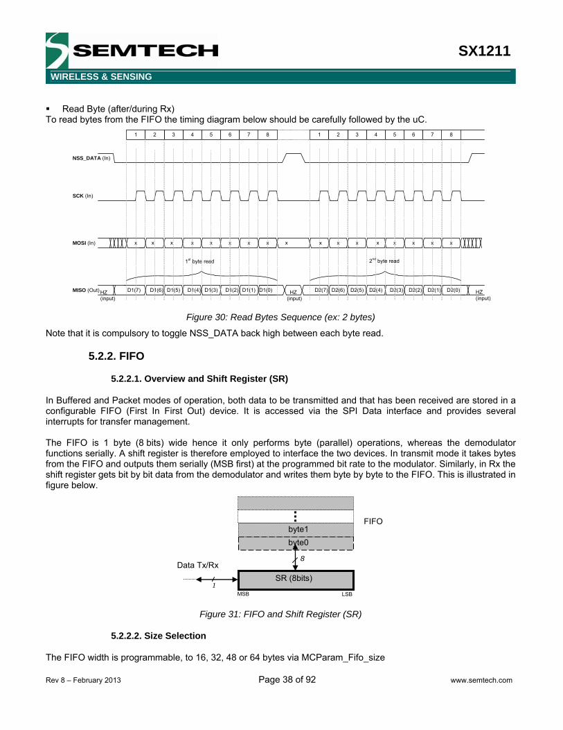
SX1211
WIRELESS & SENSING
Rev 8 – February 2013 Page 38 of 92 www.semtech.com
Read Byte (after/during Rx)
To read bytes from the FIFO the timing diagram below should be carefully followed by the uC.
SCK (In)
MISO (Out) D1(6) D1(5) D1(4) D1(3) D1(2) D1(1) D2(7) D2(6) D2(5) D2(4) D2(3) D2(2) D2(1) D2(0)D1(0)
1st byte read
D1(7) HZ (input)
HZ (input)
MOSI (In) x x x x x x x x x x x x x x x x
HZ (input)
NSS_DATA (In)
1 5 4 3 2 6 87 1 5 432 6 87
2nd byte read
x
Figure 30: Read Bytes Sequence (ex: 2 bytes)
Note that it is compulsory to toggle NSS_DATA back high between each byte read.
5.2.2. FIFO
5.2.2.1. Overview and Shift Register (SR)
In Buffered and Packet modes of operation, both data to be transmitted and that has been received are stored in a configurable FIFO (First In First Out) device. It is accessed via the SPI Data interface and provides several interrupts for transfer management. The FIFO is 1 byte (8 bits) wide hence it only performs byte (parallel) operations, whereas the demodulator functions serially. A shift register is therefore employed to interface the two devices. In transmit mode it takes bytes from the FIFO and outputs them serially (MSB first) at the programmed bit rate to the modulator. Similarly, in Rx the shift register gets bit by bit data from the demodulator and writes them byte by byte to the FIFO. This is illustrated in figure below.
Data Tx/Rx 8
1 SR (8bits)
byte0byte1
FIFO
MSB LSB
Figure 31: FIFO and Shift Register (SR)
5.2.2.2. Size Selection
The FIFO width is programmable, to 16, 32, 48 or 64 bytes via MCParam_Fifo_size
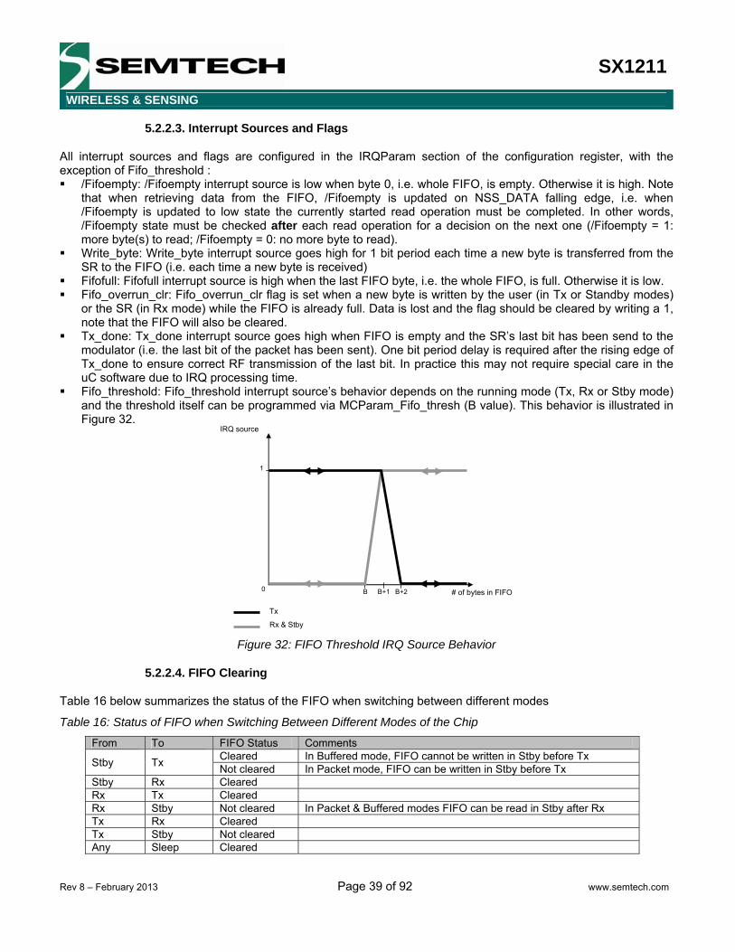
SX1211
WIRELESS & SENSING
Rev 8 – February 2013 Page 39 of 92 www.semtech.com
5.2.2.3. Interrupt Sources and Flags
All interrupt sources and flags are configured in the IRQParam section of the configuration register, with the exception of Fifo_threshold : /Fifoempty: /Fifoempty interrupt source is low when byte 0, i.e. whole FIFO, is empty. Otherwise it is high. Note
that when retrieving data from the FIFO, /Fifoempty is updated on NSS_DATA falling edge, i.e. when /Fifoempty is updated to low state the currently started read operation must be completed. In other words, /Fifoempty state must be checked after each read operation for a decision on the next one (/Fifoempty = 1: more byte(s) to read; /Fifoempty = 0: no more byte to read).
Write_byte: Write_byte interrupt source goes high for 1 bit period each time a new byte is transferred from the SR to the FIFO (i.e. each time a new byte is received)
Fifofull: Fifofull interrupt source is high when the last FIFO byte, i.e. the whole FIFO, is full. Otherwise it is low. Fifo_overrun_clr: Fifo_overrun_clr flag is set when a new byte is written by the user (in Tx or Standby modes)
or the SR (in Rx mode) while the FIFO is already full. Data is lost and the flag should be cleared by writing a 1, note that the FIFO will also be cleared.
Tx_done: Tx_done interrupt source goes high when FIFO is empty and the SR’s last bit has been send to the modulator (i.e. the last bit of the packet has been sent). One bit period delay is required after the rising edge of Tx_done to ensure correct RF transmission of the last bit. In practice this may not require special care in the uC software due to IRQ processing time.
Fifo_threshold: Fifo_threshold interrupt source’s behavior depends on the running mode (Tx, Rx or Stby mode) and the threshold itself can be programmed via MCParam_Fifo_thresh (B value). This behavior is illustrated in Figure 32.
# of bytes in FIFO
IRQ source
0
1
B B+1 B+2
Tx
Rx & Stby Figure 32: FIFO Threshold IRQ Source Behavior
5.2.2.4. FIFO Clearing
Table 16 below summarizes the status of the FIFO when switching between different modes
Table 16: Status of FIFO when Switching Between Different Modes of the Chip
From To FIFO Status Comments
Stby Tx Cleared In Buffered mode, FIFO cannot be written in Stby before Tx Not cleared In Packet mode, FIFO can be written in Stby before Tx
Stby Rx Cleared Rx Tx Cleared Rx Stby Not cleared In Packet & Buffered modes FIFO can be read in Stby after Rx Tx Rx Cleared Tx Stby Not cleared Any Sleep Cleared
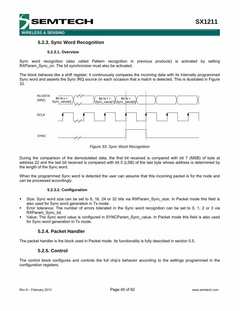
SX1211
WIRELESS & SENSING
Rev 8 – February 2013 Page 40 of 92 www.semtech.com
5.2.3. Sync Word Recognition
5.2.3.1. Overview
Sync word recognition (also called Pattern recognition in previous products) is activated by setting RXParam_Sync_on. The bit synchronizer must also be activated. The block behaves like a shift register; it continuously compares the incoming data with its internally programmed Sync word and asserts the Sync IRQ source on each occasion that a match is detected. This is illustrated in Figure 33.
Rx DATA (NRZ)
DCLK
Bit N-x = Sync_value[x]
Bit N-1 =Sync_value[1]
Bit N = Sync_value[0]
SYNC
Figure 33: Sync Word Recognition
During the comparison of the demodulated data, the first bit received is compared with bit 7 (MSB) of byte at address 22 and the last bit received is compared with bit 0 (LSB) of the last byte whose address is determined by the length of the Sync word. When the programmed Sync word is detected the user can assume that this incoming packet is for the node and can be processed accordingly.
5.2.3.2. Configuration
Size: Sync word size can be set to 8, 16, 24 or 32 bits via RXParam_Sync_size. In Packet mode this field is also used for Sync word generation in Tx mode.
Error tolerance: The number of errors tolerated in the Sync word recognition can be set to 0, 1, 2 or 3 via RXParam_Sync_tol.
Value: The Sync word value is configured in SYNCParam_Sync_value. In Packet mode this field is also used for Sync word generation in Tx mode.
5.2.4. Packet Handler
The packet handler is the block used in Packet mode. Its functionality is fully described in section 5.5.
5.2.5. Control
The control block configures and controls the full chip’s behavior according to the settings programmed in the configuration registers.
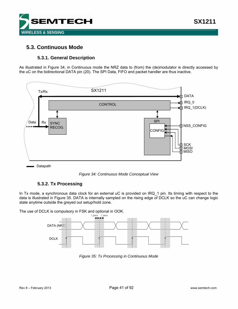
SX1211
WIRELESS & SENSING
Rev 8 – February 2013 Page 41 of 92 www.semtech.com
5.3. Continuous Mode
5.3.1. General Description
As illustrated in Figure 34, in Continuous mode the NRZ data to (from) the (de)modulator is directly accessed by the uC on the bidirectional DATA pin (20). The SPI Data, FIFO and packet handler are thus inactive.
CONTROL
CONFIG
SPI SYNC RECOG.
DATA
IRQ_1(DCLK)
MISO MOSI SCK
NSS_CONFIG Rx
Tx/Rx
IRQ_0
Datapath
SX1211
Data
Figure 34: Continuous Mode Conceptual View
5.3.2. Tx Processing
In Tx mode, a synchronous data clock for an external uC is provided on IRQ_1 pin. Its timing with respect to the data is illustrated in Figure 35. DATA is internally sampled on the rising edge of DCLK so the uC can change logic state anytime outside the greyed out setup/hold zone. The use of DCLK is compulsory in FSK and optional in OOK.
DATA (NRZ)
DCLK
T_DATAT_DATA
Figure 35: Tx Processing in Continuous Mode

SX1211
WIRELESS & SENSING
Rev 8 – February 2013 Page 42 of 92 www.semtech.com
5.3.3. Rx Processing
If the bit synchronizer is disabled, the raw demodulator output is made directly available on DATA pin and no DCLK signal is provided. Conversely, if the bit synchronizer is enabled, synchronous cleaned data and clock are made available respectively on DATA and IRQ_1 pins. DATA is sampled on the rising edge of DCLK and updated on the falling edge as illustrated in Figure 36.
DATA (NRZ)
DCLK
Figure 36: Rx Processing in Continuous Mode
Note that in Continuous mode it is always recommended to enable the bit synchronizer to clean the DATA signal even if the DCLK signal is not used by the uC. (bit synchronizer is automatically enabled in Buffered and Packet mode).
5.3.4. Interrupt Signals Mapping
The tables below give the description of the interrupts available in Continuous mode.
Rx_stby_irq_0 Rx
IRQ_0 00 (d) Sync
01 RSSI 1x -
IRQ_1 DCLK
Table 17: Interrupt Mapping in Continuous Rx Mode
Note: In Continuous mode, no interrupt is available in Stby mode
TxIRQ_0 -
IRQ_1 DCLK
Table 18: Interrupt Mapping in Continuous Tx Mode
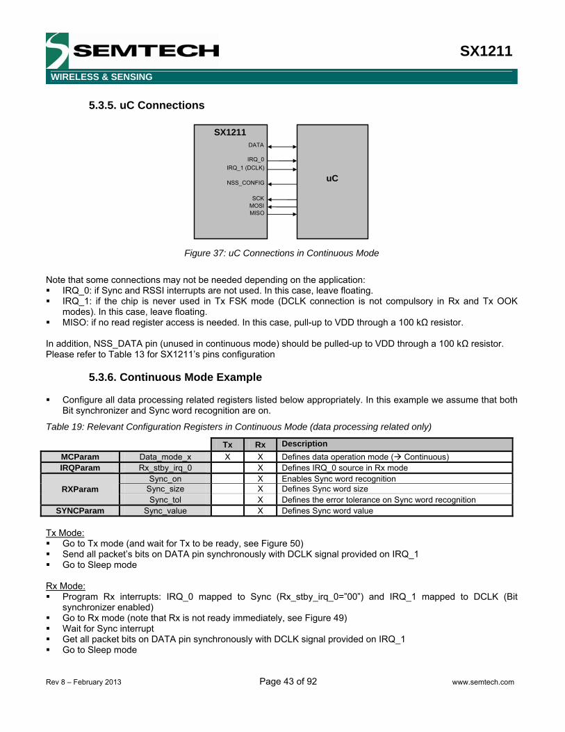
SX1211
WIRELESS & SENSING
Rev 8 – February 2013 Page 43 of 92 www.semtech.com
5.3.5. uC Connections
uC
SX1211
IRQ_0 IRQ_1 (DCLK)
DATA
NSS_CONFIG
SCKMOSIMISO
Figure 37: uC Connections in Continuous Mode
Note that some connections may not be needed depending on the application: IRQ_0: if Sync and RSSI interrupts are not used. In this case, leave floating. IRQ_1: if the chip is never used in Tx FSK mode (DCLK connection is not compulsory in Rx and Tx OOK
modes). In this case, leave floating. MISO: if no read register access is needed. In this case, pull-up to VDD through a 100 kΩ resistor.
In addition, NSS_DATA pin (unused in continuous mode) should be pulled-up to VDD through a 100 kΩ resistor. Please refer to Table 13 for SX1211’s pins configuration
5.3.6. Continuous Mode Example
Configure all data processing related registers listed below appropriately. In this example we assume that both Bit synchronizer and Sync word recognition are on.
Table 19: Relevant Configuration Registers in Continuous Mode (data processing related only)
Tx Rx DescriptionMCParam Data_mode_x X X Defines data operation mode ( Continuous) IRQParam Rx_stby_irq_0 X Defines IRQ_0 source in Rx mode
RXParam Sync_on X Enables Sync word recognition
Sync_size X Defines Sync word size Sync_tol X Defines the error tolerance on Sync word recognition
SYNCParam Sync_value X Defines Sync word value Tx Mode: Go to Tx mode (and wait for Tx to be ready, see Figure 50) Send all packet’s bits on DATA pin synchronously with DCLK signal provided on IRQ_1 Go to Sleep mode
Rx Mode: Program Rx interrupts: IRQ_0 mapped to Sync (Rx_stby_irq_0=”00”) and IRQ_1 mapped to DCLK (Bit
synchronizer enabled) Go to Rx mode (note that Rx is not ready immediately, see Figure 49) Wait for Sync interrupt Get all packet bits on DATA pin synchronously with DCLK signal provided on IRQ_1 Go to Sleep mode

SX1211
WIRELESS & SENSING
Rev 8 – February 2013 Page 44 of 92 www.semtech.com
5.4. Buffered Mode
5.4.1. General Description
As illustrated in Figure 38, for Buffered mode operation the NRZ data to (from) the (de)modulator is not directly accessed by the uC but stored in the FIFO and accessed via the SPI Data interface. This frees the uC for other tasks between processing data from the SX1211, furthermore it simplifies software development and reduces uC performance requirements (speed, reactivity). Note that in this mode the packet handler stays inactive. An important feature is also the ability to empty the FIFO in Stby mode, ensuring low power consumption and adding greater software flexibility.
CONTROL
FIFO (+SR)
DATA
CONFIG
SPISYNC
RECOG.
IRQ_0
IRQ_1
MISO MOSI SCK NSS_DATA
NSS_CONFIG Rx
Tx
Datapath
SX1211
Data
Figure 38: Buffered Mode Conceptual View
Note that Bit Synchronizer is automatically enabled in Buffered mode. The Sync word recognition must be enabled (RXParam_Sync_on=1) independently of the FIFO filling method selected (IRQParam_Fifo_fill_method).
5.4.2. Tx Processing
After entering Tx in Buffered mode, the chip expects the uC to write into the FIFO, via the SPI Data interface, all the data bytes to be transmitted (preamble, Sync word, payload...). Actual transmission of first byte will start either when the FIFO is not empty (i.e. first byte written by the uC) or when the FIFO is full depending on bit IRQParam_Tx_start_irq_0. In Buffered mode the packet length is not limited, i.e. as long as there are bytes inside the FIFO they are sent. When the last byte is transferred to the SR, /Fifoempty IRQ source is asserted to warn the uC, at that time FIFO can still be filled with additional bytes if needed. When the last bit of the last byte has left the SR (i.e. 8 bit periods later), the Tx_done interrupt source is asserted and the user can exit Tx mode after waiting at least 1 bit period from the last bit processed by modulator.
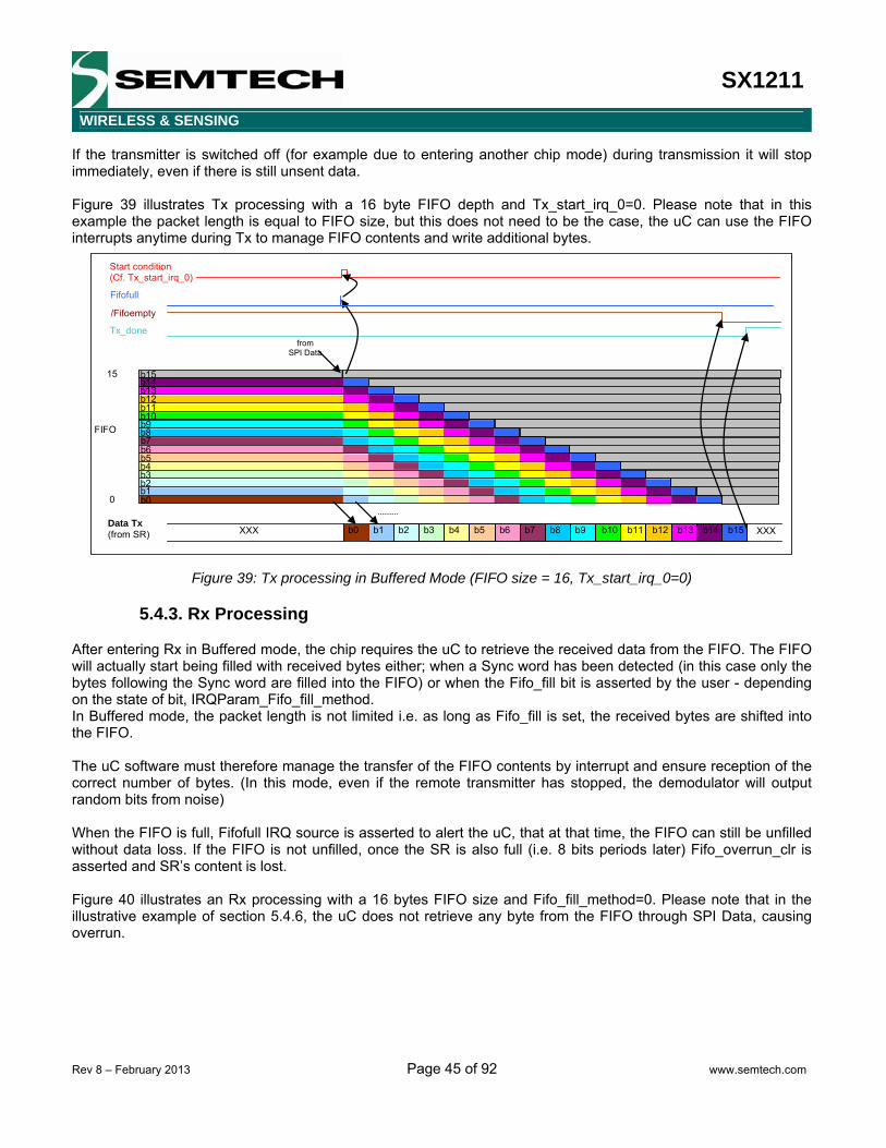
SX1211
WIRELESS & SENSING
Rev 8 – February 2013 Page 45 of 92 www.semtech.com
If the transmitter is switched off (for example due to entering another chip mode) during transmission it will stop immediately, even if there is still unsent data. Figure 39 illustrates Tx processing with a 16 byte FIFO depth and Tx_start_irq_0=0. Please note that in this example the packet length is equal to FIFO size, but this does not need to be the case, the uC can use the FIFO interrupts anytime during Tx to manage FIFO contents and write additional bytes.
b0 b1 b2 b3 b4 b5 b6 b7 b8 b9 b10 b11 b14 b15b12 b13
b0 b1
FIFO
0
15
Data Tx (from SR)
Start condition (Cf. Tx_start_irq_0)
/Fifoempty Fifofull
Tx_done
b5
b2 b3 b4 b6 b7 b8 b9 b10 b11 b12 b13 b14 b15
XXX XXX
from SPI Data
Figure 39: Tx processing in Buffered Mode (FIFO size = 16, Tx_start_irq_0=0)
5.4.3. Rx Processing
After entering Rx in Buffered mode, the chip requires the uC to retrieve the received data from the FIFO. The FIFO will actually start being filled with received bytes either; when a Sync word has been detected (in this case only the bytes following the Sync word are filled into the FIFO) or when the Fifo_fill bit is asserted by the user - depending on the state of bit, IRQParam_Fifo_fill_method. In Buffered mode, the packet length is not limited i.e. as long as Fifo_fill is set, the received bytes are shifted into the FIFO. The uC software must therefore manage the transfer of the FIFO contents by interrupt and ensure reception of the correct number of bytes. (In this mode, even if the remote transmitter has stopped, the demodulator will output random bits from noise) When the FIFO is full, Fifofull IRQ source is asserted to alert the uC, that at that time, the FIFO can still be unfilled without data loss. If the FIFO is not unfilled, once the SR is also full (i.e. 8 bits periods later) Fifo_overrun_clr is asserted and SR’s content is lost. Figure 40 illustrates an Rx processing with a 16 bytes FIFO size and Fifo_fill_method=0. Please note that in the illustrative example of section 5.4.6, the uC does not retrieve any byte from the FIFO through SPI Data, causing overrun.

SX1211
WIRELESS & SENSING
Rev 8 – February 2013 Page 46 of 92 www.semtech.com
b0 b1 b2 b3 b4 b5 b6 b7 b8 b9 b10 b11 b14 b15b12 b13 b16Sync Preamble “noisy” data
b0b1
b5
b2b3
b4
b6b7
b8b9
b10 b11
b12 b13
b14b15
0
15
Data Rx (to SR) Start condition (Cf. Fifo_fill_method) /Fifoempty Fifofull Fifo_overrun_clr Write_byte
FIFO
Figure 40: Rx Processing in Buffered Mode (FIFO size=16, Fifo_fill_method=0)
5.4.4. Interrupt Signals Mapping
The tables below describe the interrupts available in Buffered mode.
Rx_stby_irq_x Rx Stby
IRQ_0
00 (d) - - 01 Write_byte - 10 /Fifoempty /Fifoempty 11 Sync -
IRQ_1
00 (d) - - 01 Fifofull Fifofull 10 RSSI - 11 Fifo_threshold Fifo_threshold
Table 20: Interrupt Mapping in Buffered Rx and Stby Modes
Tx
IRQ_0 /Fifoempty
IRQ_1 Tx_irq_1=0 (d) Fifofull Tx_irq_1=1 Tx_done
Table 21: Interrupt Mapping in Buffered Tx Mode

SX1211
WIRELESS & SENSING
Rev 8 – February 2013 Page 47 of 92 www.semtech.com
5.4.5. uC Connections
uC
SX1211
IRQ_0 IRQ_1
NSS_CONFIG
SCKMOSIMISO
NSS_DATA
Figure 41: uC Connections in Buffered Mode
Note that depending upon the application, some uC connections may not be needed: IRQ_0: if none of the relevant IRQ sources are used. In this case, leave floating. IRQ_1: if none of the relevant IRQ sources are used. In this case, leave floating. MISO: if no read register access is needed and the chip is used in Tx mode only. In this case, pull up to VDD
through a 100 kΩ resistor. In addition, DATA pin (unused in buffered mode) should be pulled-up to VDD through a 100 kΩ resistor. Please refer to Table 13 for the SX1211’s pin configuration.
5.4.6. Buffered Mode Example
Configure all data processing related registers listed below appropriately. In this example we assume Sync word recognition is on and Fifo_fill_method=0.
Tx Rx Description
MCParam Data_mode_x X X Defines data operation mode ( Buffered)
Fifo_size X X Defines FIFO size Fifo_thresh X X Defines FIFO threshold
IRQParam
Rx_stby_irq_0 X Defines IRQ_0 source in Rx & Stby modes Rx_stby_irq_1 X Defines IRQ_1 source in Rx & Stby modes
Tx_irq_1 X Defines IRQ_1 source in Tx mode Fifo_fill_method X Defines FIFO filling method
Fifo_fill X Controls FIFO filling status Tx_start_irq_0 X Defines Tx start condition and IRQ_0 source
RXParam Sync_size X Defines Sync word size Sync_tol X Defines the error tolerance on Sync word detection
SYNCParam Sync_value X Defines Sync word value
Table 22: Relevant Configuration Registers in Buffered Mode (data processing related only)
Tx Mode: Program Tx start condition and IRQs: Start Tx when FIFO is not empty (Tx_start_irq_0=1) and IRQ_1 mapped
to Tx_done (Tx_irq_1=1) Go to Tx mode (and wait for Tx to be ready, see Figure 50)

SX1211
WIRELESS & SENSING
Rev 8 – February 2013 Page 48 of 92 www.semtech.com
Write packet bytes into FIFO. Tx starts when the first byte is written (Tx_start_irq_0=1). We assume the FIFO is being filled via SPI Data faster than being unfilled by SR.
Wait for Tx_done interrupt (+1 bit period) Go to Sleep mode
Rx Mode: Program Rx/Stby interrupts: IRQ_0 mapped to /Fifoempty (Rx_stby_irq_0=10) and IRQ_1 mapped to
Fifo_threshold (Rx_stby_irq_1=11). Configure Fifo_thresh to an appropriate value (ex: to detect packet end if its length is known)
Go to Rx mode (note that Rx is not ready immediately, Cf section 7.3.1). Wait for Fifo_threshold interrupt (i.e. Sync word has been detected and FIFO filled up to the defined threshold). If it is packet end, go to Stby (SR’s content is lost). Read packet bytes from FIFO until /Fifoempty goes low (or correct number of bytes is read). Go to Sleep mode.
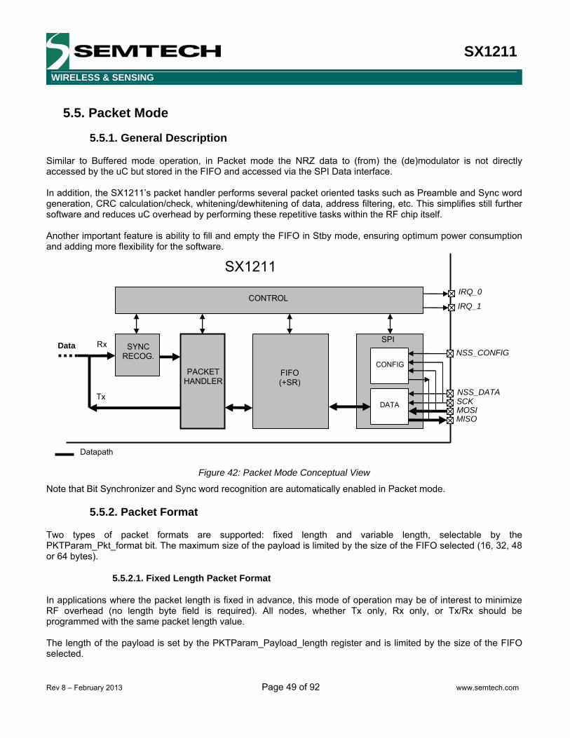
SX1211
WIRELESS & SENSING
Rev 8 – February 2013 Page 49 of 92 www.semtech.com
5.5. Packet Mode
5.5.1. General Description
Similar to Buffered mode operation, in Packet mode the NRZ data to (from) the (de)modulator is not directly accessed by the uC but stored in the FIFO and accessed via the SPI Data interface. In addition, the SX1211’s packet handler performs several packet oriented tasks such as Preamble and Sync word generation, CRC calculation/check, whitening/dewhitening of data, address filtering, etc. This simplifies still further software and reduces uC overhead by performing these repetitive tasks within the RF chip itself. Another important feature is ability to fill and empty the FIFO in Stby mode, ensuring optimum power consumption and adding more flexibility for the software.
CONTROL
DATA
CONFIG
SPI
PACKET HANDLER
SYNC RECOG.
IRQ_0
IRQ_1
MISO MOSI SCK NSS_DATA
NSS_CONFIG Rx
Tx
Datapath
SX1211
Data
FIFO (+SR)
Figure 42: Packet Mode Conceptual View
Note that Bit Synchronizer and Sync word recognition are automatically enabled in Packet mode.
5.5.2. Packet Format
Two types of packet formats are supported: fixed length and variable length, selectable by the PKTParam_Pkt_format bit. The maximum size of the payload is limited by the size of the FIFO selected (16, 32, 48 or 64 bytes).
5.5.2.1. Fixed Length Packet Format
In applications where the packet length is fixed in advance, this mode of operation may be of interest to minimize RF overhead (no length byte field is required). All nodes, whether Tx only, Rx only, or Tx/Rx should be programmed with the same packet length value. The length of the payload is set by the PKTParam_Payload_length register and is limited by the size of the FIFO selected.
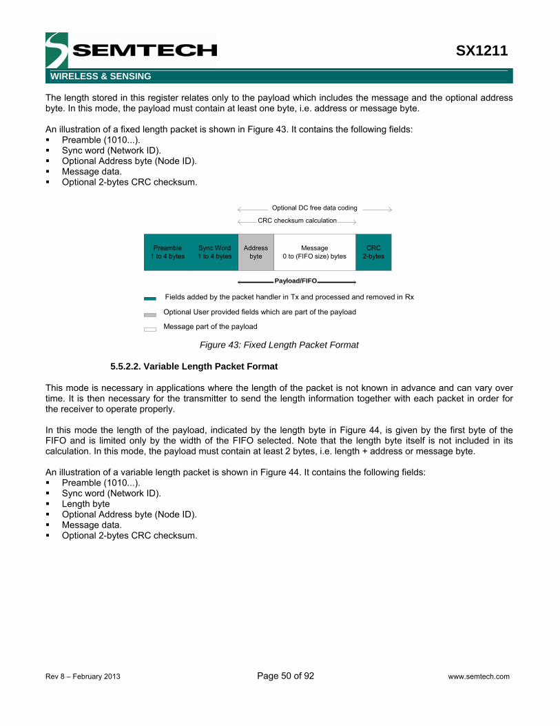
SX1211
WIRELESS & SENSING
Rev 8 – February 2013 Page 50 of 92 www.semtech.com
The length stored in this register relates only to the payload which includes the message and the optional address byte. In this mode, the payload must contain at least one byte, i.e. address or message byte. An illustration of a fixed length packet is shown in Figure 43. It contains the following fields: Preamble (1010...). Sync word (Network ID). Optional Address byte (Node ID). Message data. Optional 2-bytes CRC checksum.
Message0 to (FIFO size) bytes
Addressbyte
CRC2-bytes
Sync Word1 to 4 bytes
Preamble 1 to 4 bytes
Payload/FIFO
CRC checksum calculation
Fields added by the packet handler in Tx and processed and removed in Rx
Optional User provided fields which are part of the payload
Message part of the payload
Optional DC free data coding
Figure 43: Fixed Length Packet Format
5.5.2.2. Variable Length Packet Format
This mode is necessary in applications where the length of the packet is not known in advance and can vary over time. It is then necessary for the transmitter to send the length information together with each packet in order for the receiver to operate properly. In this mode the length of the payload, indicated by the length byte in Figure 44, is given by the first byte of the FIFO and is limited only by the width of the FIFO selected. Note that the length byte itself is not included in its calculation. In this mode, the payload must contain at least 2 bytes, i.e. length + address or message byte. An illustration of a variable length packet is shown in Figure 44. It contains the following fields: Preamble (1010...). Sync word (Network ID). Length byte Optional Address byte (Node ID). Message data. Optional 2-bytes CRC checksum.
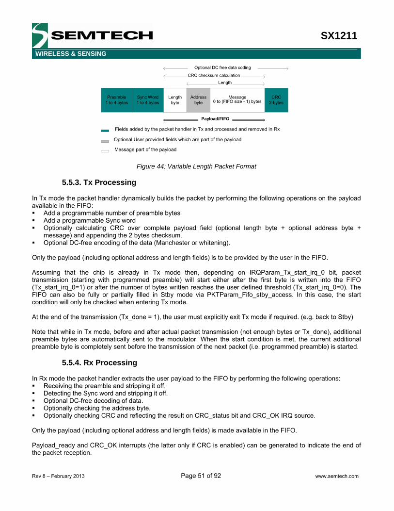
SX1211
WIRELESS & SENSING
Rev 8 – February 2013 Page 51 of 92 www.semtech.com
Message0 to (FIFO size - 1) bytes
Addressbyte
Lengthbyte
CRC 2-bytes
Sync Word1 to 4 bytes
Preamble 1 to 4 bytes
Payload/FIFO
CRC checksum calculation
Fields added by the packet handler in Tx and processed and removed in Rx
Optional User provided fields which are part of the payload
Message part of the payload
Optional DC free data coding
Length
Figure 44: Variable Length Packet Format
5.5.3. Tx Processing
In Tx mode the packet handler dynamically builds the packet by performing the following operations on the payload available in the FIFO: Add a programmable number of preamble bytes Add a programmable Sync word Optionally calculating CRC over complete payload field (optional length byte + optional address byte +
message) and appending the 2 bytes checksum. Optional DC-free encoding of the data (Manchester or whitening).
Only the payload (including optional address and length fields) is to be provided by the user in the FIFO. Assuming that the chip is already in Tx mode then, depending on IRQParam_Tx_start_irq_0 bit, packet transmission (starting with programmed preamble) will start either after the first byte is written into the FIFO (Tx_start_irq_0=1) or after the number of bytes written reaches the user defined threshold (Tx_start_irq_0=0). The FIFO can also be fully or partially filled in Stby mode via PKTParam_Fifo_stby_access. In this case, the start condition will only be checked when entering Tx mode. At the end of the transmission (Tx_done = 1), the user must explicitly exit Tx mode if required. (e.g. back to Stby) Note that while in Tx mode, before and after actual packet transmission (not enough bytes or Tx_done), additional preamble bytes are automatically sent to the modulator. When the start condition is met, the current additional preamble byte is completely sent before the transmission of the next packet (i.e. programmed preamble) is started.
5.5.4. Rx Processing
In Rx mode the packet handler extracts the user payload to the FIFO by performing the following operations: Receiving the preamble and stripping it off. Detecting the Sync word and stripping it off. Optional DC-free decoding of data. Optionally checking the address byte. Optionally checking CRC and reflecting the result on CRC_status bit and CRC_OK IRQ source.
Only the payload (including optional address and length fields) is made available in the FIFO. Payload_ready and CRC_OK interrupts (the latter only if CRC is enabled) can be generated to indicate the end of the packet reception.
SX1211
WIRELESS & SENSING
Rev 8 – February 2013 Page 52 of 92 www.semtech.com
By default, if the CRC check is enabled and fails for the current packet, then the FIFO is automatically cleared and neither of the two interrupts are generated and new packet reception is started. This autoclear function can be disabled via PKTParam_CRC_autoclr bit and, in this case, even if CRC fails, the FIFO is not cleared and only Payload_ready IRQ source is asserted. Once fully received, the payload can also be fully or partially retrieved in Stby mode via PKTParam_Fifo_stby_access. At the end of the reception, although the FIFO automatically stops being filled, it is still up to the user to explicitly exit Rx mode if required. (e.g. go to Stby to get payload). FIFO must be empty for a new packet reception to start.
5.5.5. Packet Filtering
SX1211’s packet handler offers several mechanisms for packet filtering ensuring that only useful packets are made available to the uC, reducing significantly system power consumption and software complexity.
5.5.5.1. Sync Word Based
Sync word filtering/recognition is automatically enabled in Packet mode. It is used for identifying the start of the payload and also for network identification. As previously described, the Sync word recognition block is configured (size, error tolerance, value) via RXParam_Sync_size, RXParam_Sync_tol and SYNCParam configuration registers. This information is used, both for appending Sync word in Tx, and filtering packets in Rx. Every received packet which does not start with this locally configured Sync word is automatically discarded and no interrupt is generated. When the Sync word is detected, payload reception automatically starts and Sync IRQ source is asserted.
5.5.5.2. Address Based
Address filtering can be enabled via the PKTParam_Adrs_filt bits. It adds another level of filtering, above Sync word, typically useful in a multi-node networks where a network ID is shared between all nodes (Sync word) and each node has its own ID (address). Three address based filtering options are available: Adrs_filt = 01: Received address field is compared with internal register Node_Adrs. If they match then the
packet is accepted and processed, otherwise it is discarded. Adrs_filt = 10: Received address field is compared with internal register Node_Adrs and the constant 0x00. If
either is a match, the received packet is accepted and processed, otherwise it is discarded. This additional check with a constant is useful for implementing broadcast in a multi-node networks.
Adrs_filt = 11: Received address field is compared with internal register Node_Adrs and the constants 0x00 & 0xFF. If any of the three matches, then the received packet is accepted and processed, otherwise it is discarded. These additional checks with constants are useful for implementing broadcast commands of all nodes.
Please note that the received address byte, as part of the payload, is not stripped off the packet and is made available in the FIFO. In addition, Node_Adrs and Adrs_filt only apply to Rx. On Tx side, if address filtering is expected, the address byte should simply be put into the FIFO like any other byte of the payload.
5.5.5.3. Length Based
In variable length Packet mode, PKTParam_Payload_length must be programmed with the maximum length permitted. If received length byte is smaller than this maximum then the packet is accepted and processed, otherwise it is discarded.
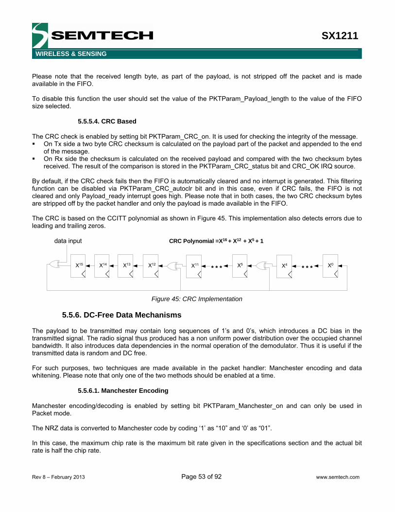
SX1211
WIRELESS & SENSING
Rev 8 – February 2013 Page 53 of 92 www.semtech.com
Please note that the received length byte, as part of the payload, is not stripped off the packet and is made available in the FIFO. To disable this function the user should set the value of the PKTParam_Payload_length to the value of the FIFO size selected.
5.5.5.4. CRC Based
The CRC check is enabled by setting bit PKTParam_CRC_on. It is used for checking the integrity of the message. On Tx side a two byte CRC checksum is calculated on the payload part of the packet and appended to the end
of the message. On Rx side the checksum is calculated on the received payload and compared with the two checksum bytes
received. The result of the comparison is stored in the PKTParam_CRC_status bit and CRC_OK IRQ source. By default, if the CRC check fails then the FIFO is automatically cleared and no interrupt is generated. This filtering function can be disabled via PKTParam_CRC_autoclr bit and in this case, even if CRC fails, the FIFO is not cleared and only Payload_ready interrupt goes high. Please note that in both cases, the two CRC checksum bytes are stripped off by the packet handler and only the payload is made available in the FIFO. The CRC is based on the CCITT polynomial as shown in Figure 45. This implementation also detects errors due to leading and trailing zeros.
X14 X13 X12 X11 X5 X0 X15
CRC Polynomial =X16 + X12 + X5 + 1
* * * X4 * * *
data input
Figure 45: CRC Implementation
5.5.6. DC-Free Data Mechanisms
The payload to be transmitted may contain long sequences of 1’s and 0’s, which introduces a DC bias in the transmitted signal. The radio signal thus produced has a non uniform power distribution over the occupied channel bandwidth. It also introduces data dependencies in the normal operation of the demodulator. Thus it is useful if the transmitted data is random and DC free. For such purposes, two techniques are made available in the packet handler: Manchester encoding and data whitening. Please note that only one of the two methods should be enabled at a time.
5.5.6.1. Manchester Encoding
Manchester encoding/decoding is enabled by setting bit PKTParam_Manchester_on and can only be used in Packet mode. The NRZ data is converted to Manchester code by coding ‘1’ as “10” and ‘0’ as “01”. In this case, the maximum chip rate is the maximum bit rate given in the specifications section and the actual bit rate is half the chip rate.
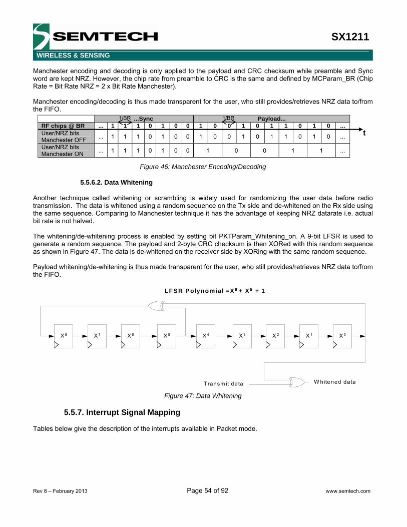
SX1211
WIRELESS & SENSING
Rev 8 – February 2013 Page 54 of 92 www.semtech.com
Manchester encoding and decoding is only applied to the payload and CRC checksum while preamble and Sync word are kept NRZ. However, the chip rate from preamble to CRC is the same and defined by MCParam_BR (Chip Rate = Bit Rate NRZ = 2 x Bit Rate Manchester). Manchester encoding/decoding is thus made transparent for the user, who still provides/retrieves NRZ data to/from the FIFO.
...Sync Payload... RF chips @ BR ... 1 1 1 0 1 0 0 1 0 0 1 0 1 1 0 1 0 ... User/NRZ bits Manchester OFF ... 1 1 1 0 1 0 0 1 0 0 1 0 1 1 0 1 0 ...
User/NRZ bits Manchester ON ... 1 1 1 0 1 0 0 1 0 0 1 1 ...
t
1/BR 1/BR
Figure 46: Manchester Encoding/Decoding
5.5.6.2. Data Whitening
Another technique called whitening or scrambling is widely used for randomizing the user data before radio transmission. The data is whitened using a random sequence on the Tx side and de-whitened on the Rx side using the same sequence. Comparing to Manchester technique it has the advantage of keeping NRZ datarate i.e. actual bit rate is not halved. The whitening/de-whitening process is enabled by setting bit PKTParam_Whitening_on. A 9-bit LFSR is used to generate a random sequence. The payload and 2-byte CRC checksum is then XORed with this random sequence as shown in Figure 47. The data is de-whitened on the receiver side by XORing with the same random sequence. Payload whitening/de-whitening is thus made transparent for the user, who still provides/retrieves NRZ data to/from the FIFO.
X 7 X 6 X 5 X 4 X 3 X 2 X 1 X 0 X 8
LFSR Polynom ial =X 9 + X 5 + 1
Transm it data W hitened data Figure 47: Data Whitening
5.5.7. Interrupt Signal Mapping
Tables below give the description of the interrupts available in Packet mode.

SX1211
WIRELESS & SENSING
Rev 8 – February 2013 Page 55 of 92 www.semtech.com
Table 23: Interrupt Mapping in Rx and Stby in Packet Mode
Rx_stby_irq_x Rx Stby
IRQ_0
00 (d) Payload_ready - 01 Write_byte - 10 /Fifoempty /Fifoempty 11 Sync or Adrs_match* -
IRQ_1
00 (d) CRC_OK - 01 Fifofull Fifofull 10 RSSI - 11 Fifo_threshold Fifo_threshold
*The latter if Address filtering is enabled
Tx
IRQ_0 Tx_start_irq_0=0 (d) Fifo_threshold Tx_start_irq_0=1 /Fifoempty
IRQ_1 Tx_irq_1=0 (d) Fifofull Tx_irq_1=1 Tx_done
Table 24: Interrupt Mapping in Tx Packet Mode
5.5.8. uC Connections
uC
SX1211
IRQ_0 IRQ_1
NSS_CONFIG
SCKMOSIMISO
NSS_DATA
Figure 48: uC Connections in Packet Mode
Note that depending upon the application, some uC connections may not be needed: IRQ_0: if none of the relevant IRQ sources are used. In this case, leave floating. IRQ_1: if none of the relevant IRQ sources are used. In this case, leave floating. MISO: if no read register access is needed and the chip is used in Tx mode only. In this case, pull up to VDD
through a 100 kΩ resistor. In addition, DATA pin (unused in packet mode) should be pulled-up to VDD through a 100 kΩ resistor. Please refer to Table 13 for the SX1211’s pin configuration.

SX1211
WIRELESS & SENSING
Rev 8 – February 2013 Page 56 of 92 www.semtech.com
5.5.9. Packet Mode Example
Configure all data processing related registers listed below appropriately. In this example we assume CRC is enabled with autoclear on.
Table 25: Relevant Configuration Registers in Packet Mode (data processing related only)
Tx Rx Description
MCParam Data_mode_x X X Defines data operation mode ( Packet)
Fifo_size X X Defines FIFO size Fifo_thresh X X Defines FIFO threshold
IRQParam
Rx_stby_irq_0 X Defines IRQ_0 source in Rx & Stby modes Rx_stby_irq_1 X Defines IRQ_1 source in Rx & Stby modes
Tx_irq_1 X Defines IRQ_1 source in Tx mode Tx_start_irq_0 X Defines Tx start condition and IRQ_0 source
RXParam Sync_size X X Defines Sync word size Sync_tol X Defines the error tolerance on Sync word detection
SYNCParam Sync_value X X Defines Sync word value
PKTParam
Manchester_on X X Enables Manchester encoding/decoding Payload_length X(1) X Length in fixed format, max Rx length in variable format
Node_adrs X Defines node address for Rx address filtering Pkt_format X X Defines packet format (fixed or variable length)
Preamble_size X Defines the size of preamble to be transmitted Whitening_on X X Enables whitening/de-whitening process
CRC_on X X Enables CRC calculation/check Adrs_filt X Enables and defines address filtering
CRC_autoclr X Enables FIFO autoclear if CRC failed Fifo_stby_access X X Defines FIFO access in Stby mode
(1)fixed format only Tx Mode: Program Tx start condition and IRQs: Start Tx when FIFO not empty (Tx_start_irq_0=1) and IRQ_1 mapped to
Tx_done (Tx_irq_1=1) Go to Stby mode Write all payload bytes into FIFO (Fifo_stby_access=0, Stby interrupts can be used if needed) Go to Tx mode. When Tx is ready (automatically handled) Tx starts (Tx_start_irq_0=1). Wait for Tx_done interrupt (+1 bit period) Go to Sleep mode
Rx Mode: Program Rx/Stby interrupts: IRQ_0 mapped to /Fifoempty (Rx_stby_irq_0=10) and IRQ_1 mapped to CRC_OK
(Rx_stby_irq_1=00) Go to Rx (note that Rx is not ready immediately, see section 7.3.1 Wait for CRC_OK interrupt Go to Stby Read payload bytes from FIFO until /Fifoempty goes low. (Fifo_stby_access =1) Go to Sleep mode
5.5.10. Additional Information
If the number of bytes filled for transmission is greater than the actual length of the packet to be transmitted and Tx_start_irq_0 = 1, then the FIFO is cleared after the packet has been transmitted. Thus the extra bytes in the
SX1211
WIRELESS & SENSING
Rev 8 – February 2013 Page 57 of 92 www.semtech.com
FIFO are lost. On the other hand if Tx_start_irq_0 = 0 then the extra bytes are kept into the FIFO. This opens up the possibility of transmitting more than one packet by filling the FIFO with multiple packet messages. It is not possible to receive multiple packets. Once a packet has been received and filled into the FIFO all its content needs to be read i.e. the FIFO must be empty for a new packet reception to be initiated. The Payload_ready interrupt goes high when the last payload byte is available in the FIFO and remains high until all its data are read. Similar behavior is applicable to Adrs_match and CRC_OK interrupts. The CRC result is available in the CRC_status bit as soon as the CRC_successful and Payload_ready interrupt sources are triggered. In Rx mode, CRC_status is cleared when the complete payload has been read from the FIFO. If the payload is read in Stby mode, then CRC_status is cleared when the user goes back to Rx mode and a new Sync word is detected. The Fifo_fill_method and Fifo_fill bits don’t have any meaning in the Packet mode and should be set to their default values only.
SX1211
WIRELESS & SENSING
Rev 8 – February 2013 Page 58 of 92 www.semtech.com
6. Configuration and Status Registers
6.1. General Description Table 26 sums-up the control and status registers of the SX1211:
Table 26: Registers List
Name Size Address DescriptionMCParam 13 x 8 0 - 12 Main parameters common to transmit and receive modes IRQParam 3 x 8 13 - 15 Interrupt registers RXParam 6 x 8 16 - 21 Receiver parameters SYNCParam 4 x 8 22 – 25 Pattern TXParam 1 x 8 26 Transmitter parameters OSCParam 1 x 8 27 Crystal oscillator parameters PKTParam 4 x 8 28 - 31 Packet handler parameters
6.2. Main Configuration Register - MCParam The detailed description of the MCParam register is given in Table 27.
Table 27: MCParam Register Description
Name Bits Address (d) RW Description
Chip_mode 7-5 0 r/w
Transceiver mode: 000 sleep mode - Sleep 001 stand-by mode - Stby (d) 010 frequency synthesizer mode - FS 011 receive mode - Rx 100 transmit mode - Tx
Freq_band 4-3 0 r/w
Frequency band: 00 902 – 915 MHz 01 915 – 928 MHz (d) 10 950 – 960 MHz or 863 - 870 MHz (Application Circuit dependant)
VCO_trim 2-1 0 r/w
Fine VCO trimming: 00 Vtune determined by tank inductors values (d) 01 Vtune + 60 mV typ. 10 Vtune + 120 mV typ. 11 Vtune + 180 mV typ.
RPS_select 0 0 r/w Selection between the two sets of frequency dividers of the PLL, Ri/Pi/Si 0 R1/P1/S1 selected(d) 1 R2/P2/S2 selected
Modul_select 7-6 1 r/w Modulation type: 01 OOK 10 FSK (d)
Data_mode_0 5 1 r/w Data operation mode LSB (refer to Data_Mode_1 (Bit 2 Addr 1)
OOK_thresh_type 4-3 1 r/w
OOK demodulator threshold type: 00 fixed threshold mode 01 peak mode (d) 10 average mode 11 reserved

SX1211
WIRELESS & SENSING
Rev 8 – February 2013 Page 59 of 92 www.semtech.com
Data_mode_1 2 1 r/w
Data operation mode’s MSB. Cf. Data_mode_0 (Bit 5 Addr 1) Data_mode_1Bit 2 addr 1
Data_mode_0Bit 5 addr 1
Data Operation Mode
0 0 Continuous (d) 0 1 Buffered 1 x Packet
IF_gain 1-0 1 r/w
Gain on the IF chain: 00 maximal gain (0dB) (d) 01 -4.5 dB 10 -9dB 11 -13.5 dB
Freq_dev 7-0 2 r/w
Single side frequency deviation in FSK Transmit mode: Refer to sections 3.3.4 and 3.3.5
Fdev = 1) (D32 +⋅
XTALf , 0 ≤ D ≤ 255, where D is the value in the register.
(d): D = “00000011” => Fdev = 100 kHz
Res 7 3 r/w Reserved (d): “0”
BR 6-0 3 r/w
Bit Rate = 1) (C64 +⋅
XTALf , 0 ≤ C ≤ 127, where C is the value in the register.
(d): C = “0000111” => Bit Rate = 25 kb/s NRZ OOK_ floor_thresh 7-0 4 r/w Floor threshold in OOK Rx mode. By default 6 dB.
(d): “00001100” assuming 0.5 dB RSSI step
Fifo_size 7:6 5 r/w
FIFO size selection: 00 16 bytes (d) 01 32 bytes 10 48 bytes 11 64 bytes
Fifo_thresh 5-0 5 r/w FIFO threshold for interrupt source (Cf section 5.2.2.3) (d): B = “001111”
R1 7-0 6 r/w R counter, active when RPS_select=”0” (d):77h; default values of R1, P1, S1 generate 915.0 MHz in FSK mode
P1 7-0 7 r/w P counter, active when RPS_select=”0” (d): 64h; default values of R1, P1, S1 generate 915.0 MHz in FSK mode
S1 7-0 8 r/w S counter, active when RPS_select=”0” (d): 32h; default values of R1, P1, S1 generate 915.0 MHz in FSK mode
R2 7-0 9 r/w R counter, active when RPS_select=”1” (d): 74h; default values of R2, P2, S2 generate 920.0 MHz in FSK mode
P2 7-0 10 r/w P counter, active when RPS_select=”1” (d): 62h; default values of R2, P2, S2 generate 920.0 MHz in FSK mode
S2 7-0 11 r/w S counter, active when RPS_select=”1” (d): 32h; default values of R2, P2, S2 generate 920.0 MHz in FSK mode
Res 7-5 12 r/w Reserved (d): “001”
PA_ramp 4-3 12 r/w
Ramp control of the rise and fall times of the Tx PA regulator output voltage in OOK mode: 00 3us 01 8.5 us 10 15 us 11 23 us (d)
Res 2-0 12 r/w Reserved (d):”000”

SX1211
WIRELESS & SENSING
Rev 8 – February 2013 Page 60 of 92 www.semtech.com
6.3. Interrupt Configuration Parameters - IRQParam The detailed description of the IRQParam register is given in Table 28.
Table 28: IRQParam Register Description
Name Bits Address (d) RW Description
Rx_stby_irq_0 7-6 13 r/w
IRQ_0 source in Rx and Standby modes: If Data_mode(1:0) = 00 (Continuous mode): 00 Sync (d) 01 RSSI 10 Sync 11 Sync If Data_mode(1:0) = 01 (Buffered mode): 00 - (d) 01 Write_byte 10 /Fifoempty* 11 Sync If Data_mode(1:0) = 1x (Packet mode): 00 Payload_ready (d) 01 Write_byte 10 /Fifoempty* 11 Sync or Adrs_match (the latter if address filtering is enabled) *also available in Standby mode (Cf sections 5.4.4 and 5.5.7)
Rx_stby_irq_1 5-4 13 r/w
IRQ_1 source in Rx and Standby modes: If Data_mode(1:0) = 00 (Continuous mode): xx DCLK If Data_mode(1:0) = 01 (Buffered mode): 00 - (d) 01 Fifofull* 10 RSSI 11 Fifo_threshold* If Data_mode(1:0) = 1x (Packet mode): 00 CRC_ok (d) 01 Fifofull* 10 RSSI 11 Fifo_threshold* *also available in Standby mode (Cf sections 5.4.4 and 5.5.7)
Tx_irq_1 3 13 r/w
IRQ_1 source in Tx mode: If Data_mode(1:0) = 00 (Continuous mode): x DCLK If Data_mode(1:0) = 01 (Buffered mode) or 1x (Packet mode): 0 Fifofull (d) 1 Tx_done
Fifofull 2 13 r Fifofull IRQ source Goes high when FIFO is full.
/Fifoempty 1 13 r /Fifoempty IRQ source Goes low when FIFO is empty
Fifo_overrun_clr 0 13 r/w/c
Goes high when an overrun error occurred. Writing a 1 clears flag and FIFO
Fifo_fill_method 7 14 r/w FIFO filling method (Buffered mode only):
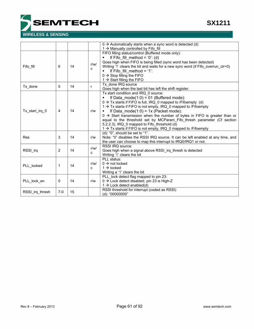
SX1211
WIRELESS & SENSING
Rev 8 – February 2013 Page 61 of 92 www.semtech.com
0 Automatically starts when a sync word is detected (d) 1 Manually controlled by Fifo_fill
Fifo_fill 6 14 r/w/c
FIFO filling status/control (Buffered mode only): If Fifo_fill_method = ‘0’: (d)
Goes high when FIFO is being filled (sync word has been detected) Writing ‘1’ clears the bit and waits for a new sync word (if Fifo_overrun_clr=0) If Fifo_fill_method = ‘1’:
0 Stop filling the FIFO 1 Start filling the FIFO
Tx_done 5 14 r Tx_done IRQ source Goes high when the last bit has left the shift register.
Tx_start_irq_0 4 14 r/w
Tx start condition and IRQ_0 source: If Data_mode(1:0) = 01 (Buffered mode):
0 Tx starts if FIFO is full, IRQ_0 mapped to /Fifoempty (d) 1 Tx starts if FIFO is not empty, IRQ_0 mapped to /Fifoempty If Data_mode(1:0) = 1x (Packet mode):
0 Start transmission when the number of bytes in FIFO is greater than or equal to the threshold set by MCParam_Fifo_thresh parameter (Cf section 5.2.2.3), IRQ_0 mapped to Fifo_threshold (d) 1 Tx starts if FIFO is not empty, IRQ_0 mapped to /Fifoempty
Res 3 14 r/w (d): “0”, should be set to “1”. Note: “0” disables the RSSI IRQ source. It can be left enabled at any time, and the user can choose to map this interrupt to IRQ0/IRQ1 or not.
RSSI_irq 2 14 r/w/c
RSSI IRQ source: Goes high when a signal above RSSI_irq_thresh is detected Writing ‘1’ clears the bit
PLL_locked 1 14 r/w/c
PLL status: 0 not locked 1 locked Writing a ‘1’ clears the bit
PLL_lock_en 0 14 r/w PLL_lock detect flag mapped to pin 23: 0 Lock detect disabled, pin 23 is High-Z 1 Lock detect enabled(d)
RSSI_irq_thresh 7-0 15 RSSI threshold for interrupt (coded as RSSI) (d): “00000000”
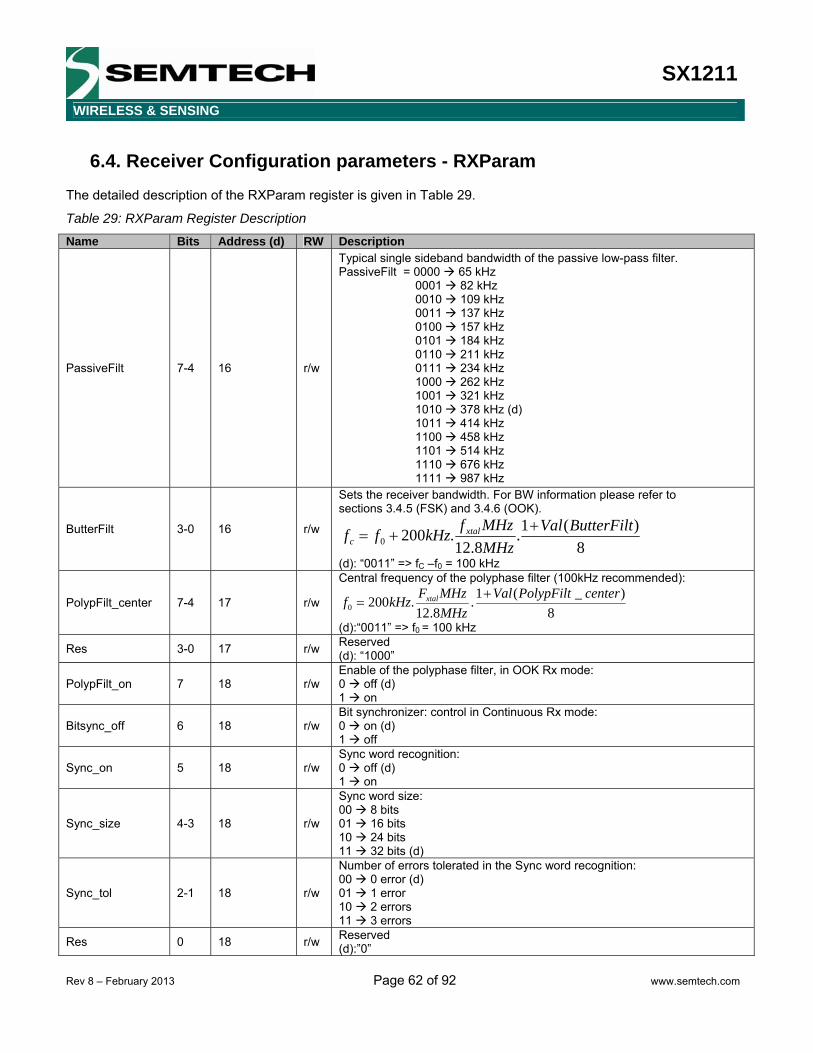
SX1211
WIRELESS & SENSING
Rev 8 – February 2013 Page 62 of 92 www.semtech.com
6.4. Receiver Configuration parameters - RXParam The detailed description of the RXParam register is given in Table 29.
Table 29: RXParam Register Description
Name Bits Address (d) RW Description
PassiveFilt 7-4 16 r/w
Typical single sideband bandwidth of the passive low-pass filter. PassiveFilt = 0000 65 kHz 0001 82 kHz 0010 109 kHz 0011 137 kHz 0100 157 kHz 0101 184 kHz 0110 211 kHz 0111 234 kHz 1000 262 kHz 1001 321 kHz 1010 378 kHz (d) 1011 414 kHz 1100 458 kHz 1101 514 kHz 1110 676 kHz 1111 987 kHz
ButterFilt 3-0 16 r/w
Sets the receiver bandwidth. For BW information please refer to sections 3.4.5 (FSK) and 3.4.6 (OOK).
8)(1.
8.12.2000
ButterFiltValMHzMHzfkHzff xtal
c+
+=
(d): “0011” => fC –f0 = 100 kHz
PolypFilt_center 7-4 17 r/w
Central frequency of the polyphase filter (100kHz recommended):
8)_(1.
8.12.2000
centerPolypFiltValMHzMHzFkHzf xtal +
=
(d):“0011” => f0 = 100 kHz
Res 3-0 17 r/w Reserved (d): “1000”
PolypFilt_on 7 18 r/w Enable of the polyphase filter, in OOK Rx mode: 0 off (d) 1 on
Bitsync_off 6 18 r/w Bit synchronizer: control in Continuous Rx mode: 0 on (d) 1 off
Sync_on 5 18 r/w Sync word recognition: 0 off (d) 1 on
Sync_size 4-3 18 r/w
Sync word size: 00 8 bits 01 16 bits 10 24 bits 11 32 bits (d)
Sync_tol 2-1 18 r/w
Number of errors tolerated in the Sync word recognition: 00 0 error (d) 01 1 error 10 2 errors 11 3 errors
Res 0 18 r/w Reserved (d):”0”
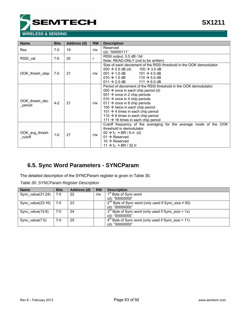
SX1211
WIRELESS & SENSING
Rev 8 – February 2013 Page 63 of 92 www.semtech.com
Name Bits Address (d) RW Description
Res 7-0 19 r/w Reserved (d): “00000111”
RSSI_val 7-0 20 r RSSI output, 0.5 dB / bit Note: READ-ONLY (not to be written)
OOK_thresh_step 7-5 21 r/w
Size of each decrement of the RSSI threshold in the OOK demodulator 000 0.5 dB (d) 100 3.0 dB 001 1.0 dB 101 4.0 dB 010 1.5 dB 110 5.0 dB 011 2.0 dB 111 6.0 dB
OOK_thresh_dec_period 4-2 21 r/w
Period of decrement of the RSSI threshold in the OOK demodulator: 000 once in each chip period (d) 001 once in 2 chip periods 010 once in 4 chip periods 011 once in 8 chip periods 100 twice in each chip period 101 4 times in each chip period 110 8 times in each chip period 111 16 times in each chip period
OOK_avg_thresh_cutoff 1-0 21 r/w
Cutoff frequency of the averaging for the average mode of the OOK threshold in demodulator 00 fC ≈ BR / 8.π (d) 01 Reserved 10 Reserved 11 fC ≈ BR / 32.π
6.5. Sync Word Parameters - SYNCParam The detailed description of the SYNCParam register is given in Table 30.
Table 30: SYNCParam Register Description
Name Bits Address (d) RW DescriptionSync_value(31:24) 7-0 22 r/w 1st Byte of Sync word
(d): “00000000” Sync_value(23:16) 7-0 23 2nd Byte of Sync word (only used if Sync_size ≠ 00)
(d): “00000000” Sync_value(15:8) 7-0 24 3rd Byte of Sync word (only used if Sync_size = 1x)
(d): “00000000” Sync_value(7:0) 7-0 25 4th Byte of Sync word (only used if Sync_size = 11)
(d): “00000000”
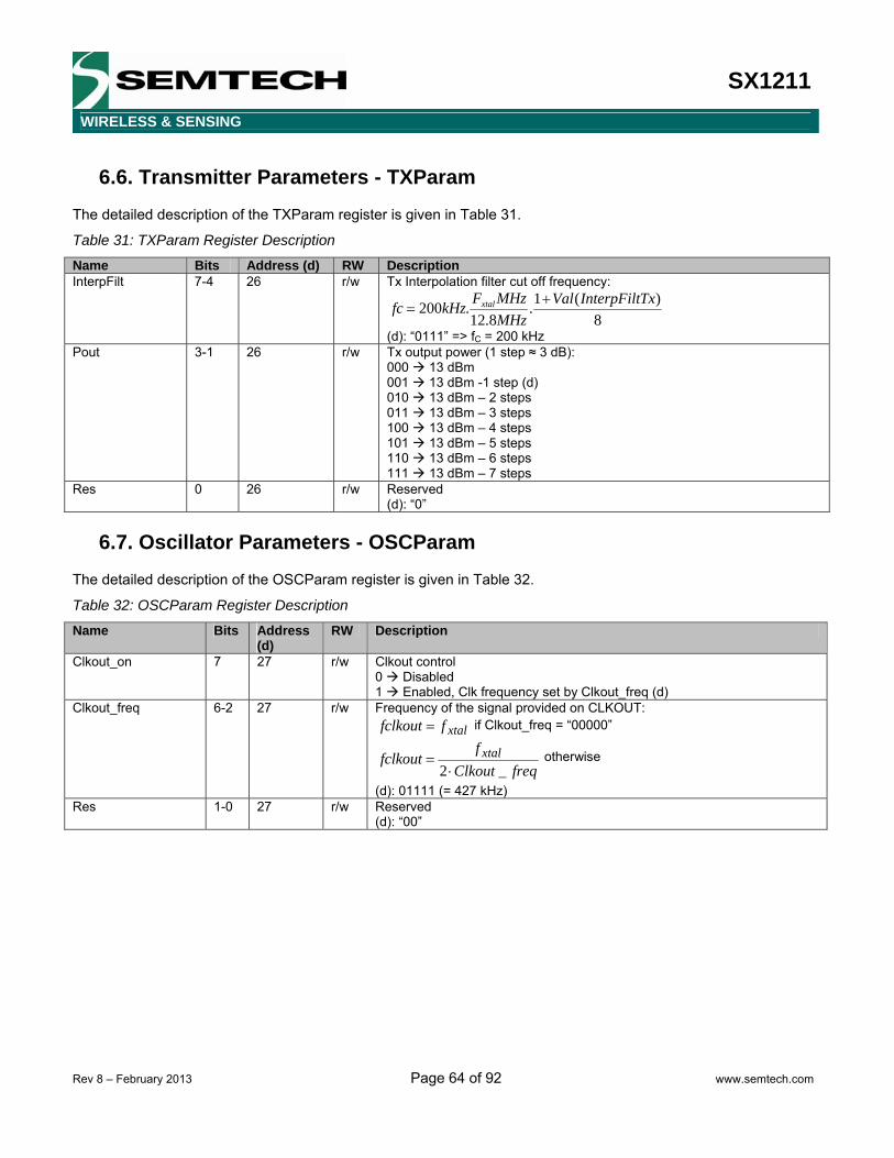
SX1211
WIRELESS & SENSING
Rev 8 – February 2013 Page 64 of 92 www.semtech.com
6.6. Transmitter Parameters - TXParam The detailed description of the TXParam register is given in Table 31.
Table 31: TXParam Register Description
Name Bits Address (d) RW DescriptionInterpFilt 7-4 26 r/w Tx Interpolation filter cut off frequency:
8)(1.
8.12.200 TxInterpFiltVal
MHzMHzFkHzfc xtal +
=
(d): “0111” => fC = 200 kHz Pout 3-1 26 r/w Tx output power (1 step ≈ 3 dB):
000 13 dBm 001 13 dBm -1 step (d) 010 13 dBm – 2 steps 011 13 dBm – 3 steps 100 13 dBm – 4 steps 101 13 dBm – 5 steps 110 13 dBm – 6 steps 111 13 dBm – 7 steps
Res 0 26 r/w Reserved (d): “0”
6.7. Oscillator Parameters - OSCParam The detailed description of the OSCParam register is given in Table 32.
Table 32: OSCParam Register Description
Name Bits Address (d)
RW Description
Clkout_on 7 27 r/w Clkout control 0 Disabled 1 Enabled, Clk frequency set by Clkout_freq (d)
Clkout_freq 6-2 27 r/w Frequency of the signal provided on CLKOUT:
xtalffclkout = if Clkout_freq = “00000”
freqClkoutf
fclkout xtal_2 ⋅
= otherwise
(d): 01111 (= 427 kHz) Res 1-0 27 r/w Reserved
(d): “00”
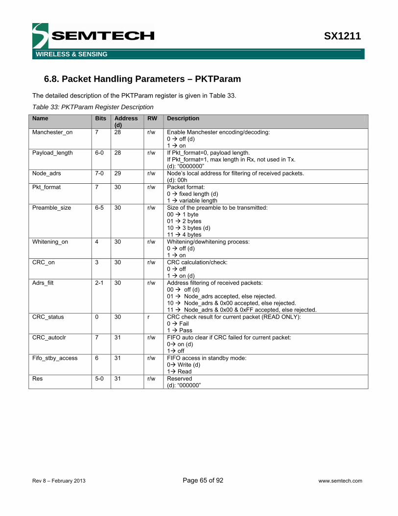
SX1211
WIRELESS & SENSING
Rev 8 – February 2013 Page 65 of 92 www.semtech.com
6.8. Packet Handling Parameters – PKTParam The detailed description of the PKTParam register is given in Table 33.
Table 33: PKTParam Register Description
Name Bits Address (d)
RW Description
Manchester_on 7 28 r/w Enable Manchester encoding/decoding: 0 off (d) 1 on
Payload_length 6-0 28 r/w If Pkt_format=0, payload length. If Pkt_format=1, max length in Rx, not used in Tx. (d): “0000000”
Node_adrs 7-0 29 r/w Node’s local address for filtering of received packets. (d): 00h
Pkt_format 7 30 r/w Packet format: 0 fixed length (d) 1 variable length
Preamble_size 6-5 30 r/w Size of the preamble to be transmitted: 00 1 byte 01 2 bytes 10 3 bytes (d) 11 4 bytes
Whitening_on 4 30 r/w Whitening/dewhitening process: 0 off (d) 1 on
CRC_on 3 30 r/w CRC calculation/check: 0 off 1 on (d)
Adrs_filt 2-1 30 r/w Address filtering of received packets: 00 off (d) 01 Node_adrs accepted, else rejected. 10 Node_adrs & 0x00 accepted, else rejected. 11 Node_adrs & 0x00 & 0xFF accepted, else rejected.
CRC_status 0 30 r CRC check result for current packet (READ ONLY): 0 Fail 1 Pass
CRC_autoclr 7 31 r/w FIFO auto clear if CRC failed for current packet: 0 on (d) 1 off
Fifo_stby_access 6 31 r/w FIFO access in standby mode: 0 Write (d) 1 Read
Res 5-0 31 r/w Reserved (d): “000000”
SX1211
WIRELESS & SENSING
Rev 8 – February 2013 Page 66 of 92 www.semtech.com
7. Application Information
7.1. Crystal Resonator Specification Table 34 shows the crystal resonator specification for the crystal reference oscillator circuit of the SX1211. This specification covers the full range of operation of the SX1211 and is employed in the reference design (see section 7.5.3).
Table 34: Crystal Resonator Specification
Name Description Min. Typ. Max. Unit Fxtal Nominal frequency 9 12.800 15 MHz Cload Load capacitance for Fxtal 10 15 16.5 pF Rm Motional resistance - - 100 ohms Co Shunt capacitance 1 - 7 pF ΔFxtal Calibration tolerance at 25+/-3°C -15 - +15 ppm ΔFxtal(ΔT) Stability over temperature range [-40°C ; +85°C] -20 - +20 ppm
ΔFxtal(Δt) Ageing tolerance in first 5 years -2 - +2 ppm/year
Note that the initial frequency tolerance, temperature stability and ageing performance should be chosen in accordance with the target operating temperature range and the receiver bandwidth selected.
7.2. Software for Frequency Calculation The R1, P1, S1, and R2, P2, S2 dividers are configured over the SPI interface and programmed by 8 bits each, at addresses 6 to 11. The frequency pairs may hence be switched in a single SPI cycle.
7.2.1. GUI
To aid the user with calculating appropriate R, P and S values, software is available to perform the frequency calculation. The SX1211 PLL frequency Calculator Software can be downloaded from the Semtech website.
7.2.2. .dll for Automatic Production Bench
The Dynamically Linked Library (DLL) used by the software to perform these calculations is also provided, free of charge, to users, for inclusion in automatic production testing. Key benefits of this are: No hand trimming of the reference frequency required: the actual reference frequency of the Device Under Test
(DUT) can be easily measured (e.g. from the CLKOUT output of the SX1211) and the tool will calculate the best frequencies to compensate for the crystal initial error.
Channel plans can be calculated and stored in the application’s memory, then adapted to the actual crystal oscillator frequency.
7.3. Switching Times and Procedures As an ultra-low power device, the SX1211 can be configured for low minimum average power consumption. To minimize consumption the following optimized transitions between modes are shown.
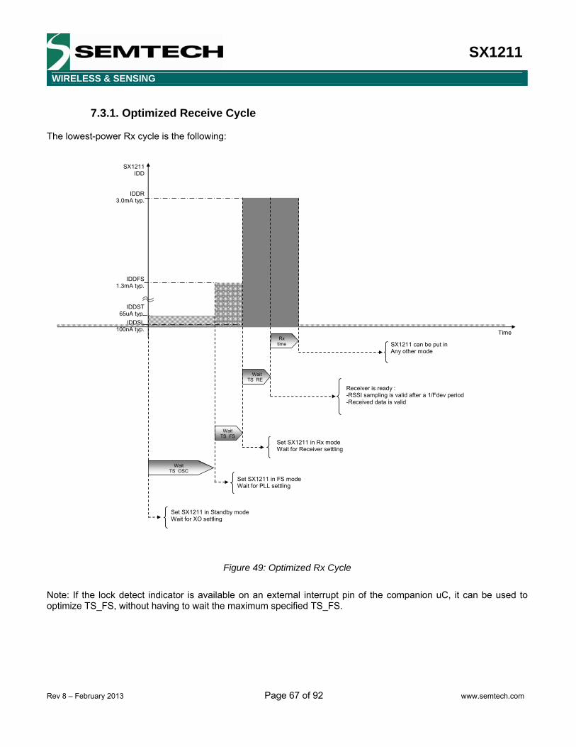
SX1211
WIRELESS & SENSING
Rev 8 – February 2013 Page 67 of 92 www.semtech.com
7.3.1. Optimized Receive Cycle
The lowest-power Rx cycle is the following:
SX1211 IDD
Time
Set SX1211 in Standby modeWait for XO settling
Set SX1211 in FS mode Wait for PLL settling
Set SX1211 in Rx mode Wait for Receiver settling
IDDR 3.0mA typ.
IDDFS 1.3mA typ.
IDDST 65uA typ.
IDDSL 100nA typ.
Wait TS OSC
Wait TS FS
Wait TS RE
Receiver is ready : -RSSI sampling is valid after a 1/Fdev period -Received data is valid
SX1211 can be put in Any other mode
Rx time
Figure 49: Optimized Rx Cycle
Note: If the lock detect indicator is available on an external interrupt pin of the companion uC, it can be used to optimize TS_FS, without having to wait the maximum specified TS_FS.

SX1211
WIRELESS & SENSING
Rev 8 – February 2013 Page 68 of 92 www.semtech.com
7.3.2. Optimized Transmit Cycle
SX1211 IDD
Time
Set SX1211 in Standby modeWait for XO settling
Set SX1211 in FS mode Wait for PLL settling
Set SX1211 in Tx mode Packet mode starts its operation
IDDT 16mA typ. @1dBm
IDDFS 1.3mA typ.
IDDST 65uA typ.
IDDSL 100nA typ.
Wait TS OSC
Wait TS FS
Wait TS TR
Data transmission can start in Continuous and Buffered modes
SX1211 can be put in Any other mode
Tx time
Figure 50: Optimized Tx Cycle
Note: As stated in the preceding section, TS_FS time can be improved by using the external lock detector pin as external interrupt trigger.
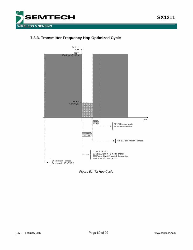
SX1211
WIRELESS & SENSING
Rev 8 – February 2013 Page 69 of 92 www.semtech.com
7.3.3. Transmitter Frequency Hop Optimized Cycle
SX1211IDD
Time
SX1211 is in Tx mode On channel 1 (R1/P1/S1)
SX1211 is now ready for data transmission
IDDT16mA typ. @1dBm
IDDFS1.3mA typ.
Wait TS HOP
Wait TS TR
Set SX1211 back in Tx mode
1. Set R2/P2/S2 2. Set SX1211 in FS mode, change MCParam_Band if needed, then switch from R1/P1/S1 to R2/P2/S2
Figure 51: Tx Hop Cycle

SX1211
WIRELESS & SENSING
Rev 8 – February 2013 Page 70 of 92 www.semtech.com
7.3.4. Receiver Frequency Hop Optimized Cycle
SX1211IDD
Time
SX1211 is in Rx mode On channel 1 (R1/P1/S1)
SX1211 is now ready for data reception
IDDR3mA typ
IDDFS1.3mA typ.
Wait TS HOP
Wait TS RE
Set SX1211 back in Rx mode
1. Set R2/P2/S2 2. Set SX1211 in FS mode, change MCParam_Band if needed, then switch from R1/P1/S1 to R2/P2/S2
Figure 52: Rx Hop Cycle
Note: it is also possible to move from one channel to the other one without having to switch off the receiver. This method is faster, and overall draws more current. For timing information, please refer to TS_RE_HOP on Table 8.
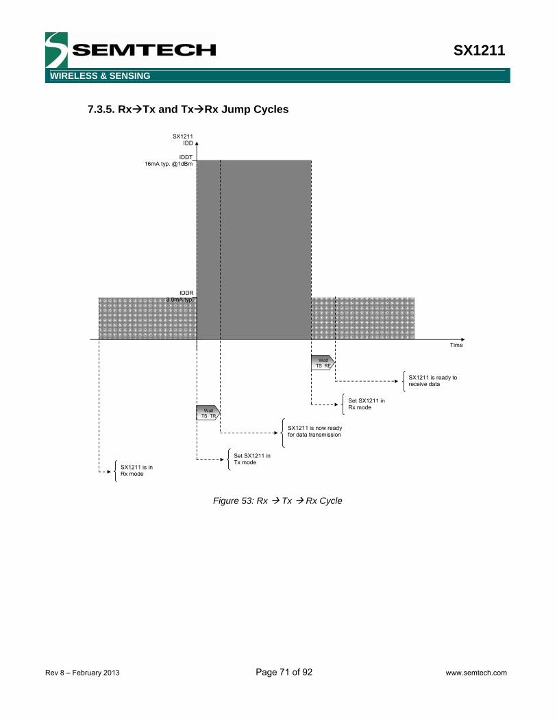
SX1211
WIRELESS & SENSING
Rev 8 – February 2013 Page 71 of 92 www.semtech.com
7.3.5. Rx Tx and Tx Rx Jump Cycles
SX1211 IDD
Time
SX1211 is in Rx mode
Set SX1211 in Tx mode
SX1211 is now ready for data transmission
IDDR 3.0mA typ.
Wait TS TR
IDDT 16mA typ. @1dBm
Set SX1211 in Rx mode
Wait TS RE
SX1211 is ready to receive data
Figure 53: Rx Tx Rx Cycle
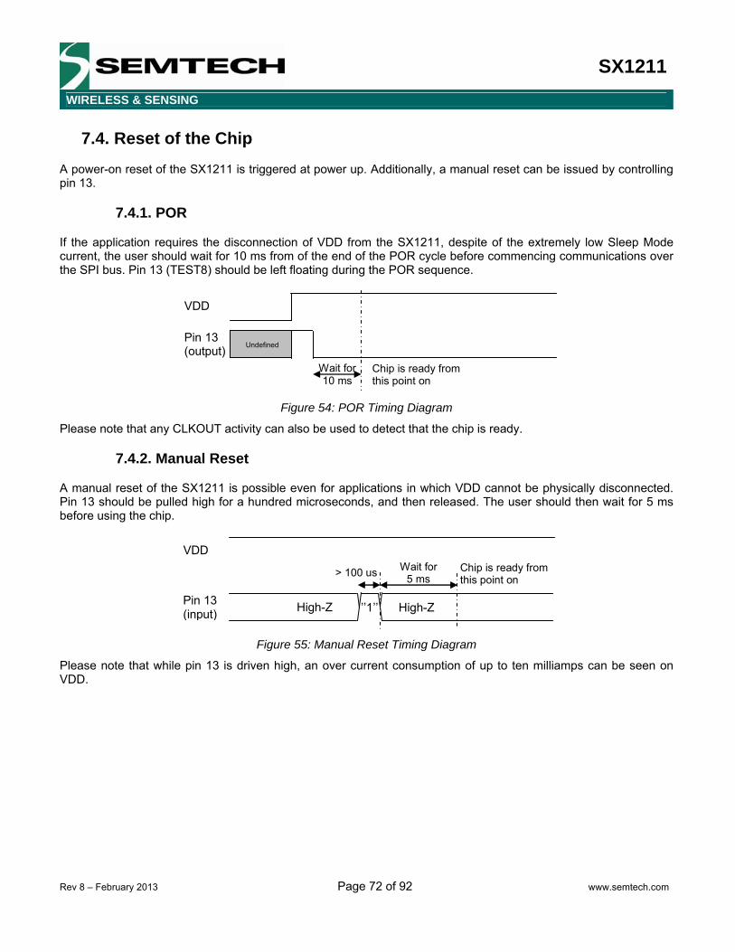
SX1211
WIRELESS & SENSING
Rev 8 – February 2013 Page 72 of 92 www.semtech.com
7.4. Reset of the Chip A power-on reset of the SX1211 is triggered at power up. Additionally, a manual reset can be issued by controlling pin 13.
7.4.1. POR
If the application requires the disconnection of VDD from the SX1211, despite of the extremely low Sleep Mode current, the user should wait for 10 ms from of the end of the POR cycle before commencing communications over the SPI bus. Pin 13 (TEST8) should be left floating during the POR sequence.
Wait for 10 ms
VDD
Pin 13 (output)
Chip is ready from this point on
Undefined
Figure 54: POR Timing Diagram
Please note that any CLKOUT activity can also be used to detect that the chip is ready.
7.4.2. Manual Reset
A manual reset of the SX1211 is possible even for applications in which VDD cannot be physically disconnected. Pin 13 should be pulled high for a hundred microseconds, and then released. The user should then wait for 5 ms before using the chip.
VDD
> 100 us Chip is ready from this point on
Pin 13 (input) High-Z High-Z’’1’’
Wait for 5 ms
Figure 55: Manual Reset Timing Diagram
Please note that while pin 13 is driven high, an over current consumption of up to ten milliamps can be seen on VDD.
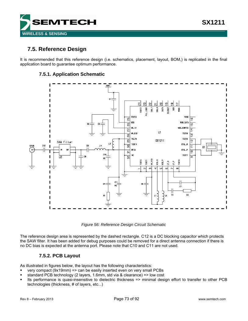
SX1211
WIRELESS & SENSING
Rev 8 – February 2013 Page 73 of 92 www.semtech.com
7.5. Reference Design It is recommended that this reference design (i.e. schematics, placement, layout, BOM,) is replicated in the final application board to guarantee optimum performance.
7.5.1. Application Schematic
Figure 56: Reference Design Circuit Schematic
The reference design area is represented by the dashed rectangle. C12 is a DC blocking capacitor which protects the SAW filter. It has been added for debug purposes could be removed for a direct antenna connection if there is no DC bias is expected at the antenna port. Please note that C10 and C11 are not used.
7.5.2. PCB Layout
As illustrated in figures below, the layout has the following characteristics: very compact (9x19mm) => can be easily inserted even on very small PCBs standard PCB technology (2 layers, 1.6mm, std via & clearance) => low cost Its performance is quasi-insensitive to dielectric thickness => minimal design effort to transfer to other PCB
technologies (thickness, # of layers, etc...)

SX1211
WIRELESS & SENSING
Rev 8 – February 2013 Page 74 of 92 www.semtech.com
The layers description is illustrated in Figure 57:
Signal (35um)
Isolation (FR4, 1.6mm)
Ground plane
Figure 57: Reference Design‘s Stackup
The layout itself is illustrated in Figure 58. Please contact Semtech for gerber files.
19mm
9mm
Figure 58: Reference Design Layout (top view)
7.5.3. Bill Of Material
Table 35: Reference Design BOM
Value Ref 868MHz 915MHz
Tol (+/-) Techno Size Comment
U1 SX1211 - Transceiver IC TQFN-32 - U2 869 MHz 915 MHz - SAW Filter 3.8*3.8 mm Plotted in section 7.5.4 Q1 12.8 MHz 15 ppm at 25°C
20 ppm over -40/+85°C 2ppm/year max
AT-cut 5.0*3.2 mm Fundamental, Cload=15 pF
R1 1Ω 1% - 0402 PA regulator R2 6.8 kΩ 1% - 0402 Loop filter C1 1uF 15% X5R 0402 VDD decoupling C2 1uF 15% X5R 0402 Top regulator decoupling C3 220 nF 10% X7R 0402 Digital regulator decoupling C4 47 nF 10% X7R 0402 PA regulator decoupling C5 100 nF 10% X7R 0402 VCO regulator decoupling C6 10 nF 10% X7R 0402 Loop Filter C7 680 pF 5% NPO 0402 Loop Filter C8 1.8 pF 0.25 pF NPO 0402 Matching C9 22 pF 5% NPO 0402 DC block and L4 adjust
L1, L2 8.2 nH 6.8 nH 0.2 nH Wire wound 0402 VCO tank inductors L3 100 nH 5% Wire wound 0402 PA Choke L4 8.2 nH 5% Multilayer 0402 Matching
C10, C11 NC - - 0402 - C12* 47pF 5% NPO 0402 DC block
*Not part of the ref. design (not required for direct antenna connection). Note: for battery powered applications, a high value capacitance should be implemented in parallel with C1 (typically 10 µF) to offer a low impedance voltage source during startup sequences.

SX1211
WIRELESS & SENSING
Rev 8 – February 2013 Page 75 of 92 www.semtech.com
7.5.4. SAW Filter Plot
The following screenshot shows the plot of the SAW filter used on the reference design:
-80
-70
-60
-50
-40
-30
-20
-10
0
400 600 800 1000 1200 1400 1600 1800 2000
Frequency [MHz]
Atte
nuat
ion
[dB]
Figure 59: 915 MHz SAW Filter Plot
-80
-70
-60
-50
-40
-30
-20
-10
0
400 600 800 1000 1200 1400 1600 1800 2000
Frequency [MHz]
Atte
nuat
ion
[dB]
Figure 60: 869 MHz SAW Filter Plot
7.5.5. Ordering Information for Tools
The modules described in section 7.5 can be ordered through your Semtech representative for evaluation purpose:
Table 36: Tools Ordering Information
Part Number Description SM1211E868 2 layer RF module, 868 MHz band SM1211E915 2 layer RF module, 915 MHz band SX1211-11SKA868 Full evaluation kit with 2 RF and controller boards, antennas and cables SX1211-11SKA915 Full evaluation kit with 2 RF and controller boards, antennas and cables
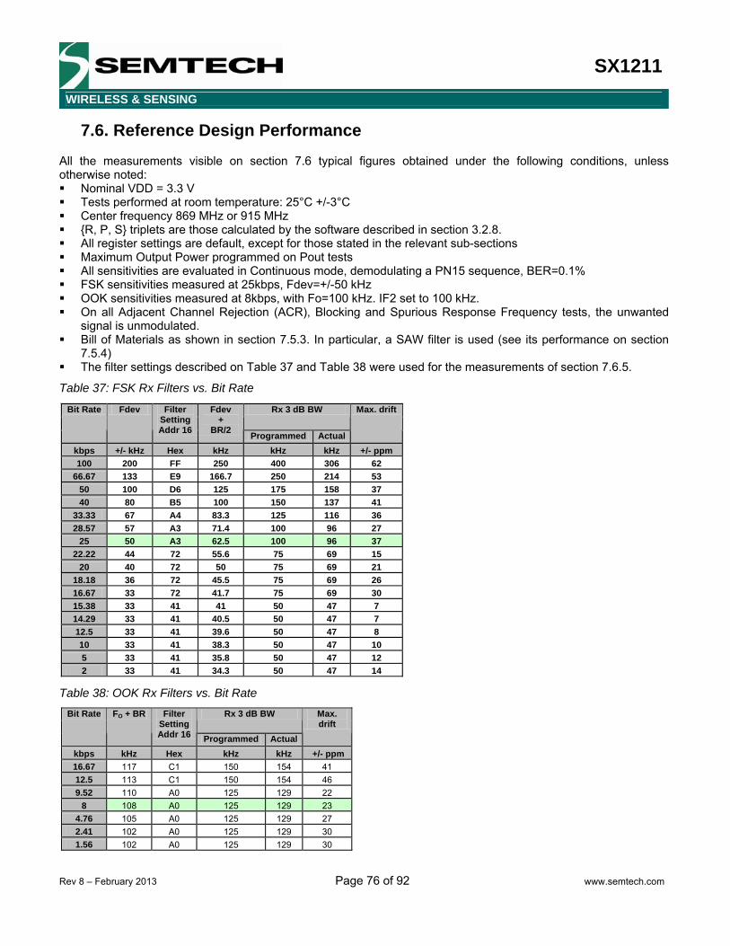
SX1211
WIRELESS & SENSING
Rev 8 – February 2013 Page 76 of 92 www.semtech.com
7.6. Reference Design Performance All the measurements visible on section 7.6 typical figures obtained under the following conditions, unless otherwise noted: Nominal VDD = 3.3 V Tests performed at room temperature: 25°C +/-3°C Center frequency 869 MHz or 915 MHz R, P, S triplets are those calculated by the software described in section 3.2.8. All register settings are default, except for those stated in the relevant sub-sections Maximum Output Power programmed on Pout tests All sensitivities are evaluated in Continuous mode, demodulating a PN15 sequence, BER=0.1% FSK sensitivities measured at 25kbps, Fdev=+/-50 kHz OOK sensitivities measured at 8kbps, with Fo=100 kHz. IF2 set to 100 kHz. On all Adjacent Channel Rejection (ACR), Blocking and Spurious Response Frequency tests, the unwanted
signal is unmodulated. Bill of Materials as shown in section 7.5.3. In particular, a SAW filter is used (see its performance on section
7.5.4) The filter settings described on Table 37 and Table 38 were used for the measurements of section 7.6.5.
Table 37: FSK Rx Filters vs. Bit Rate
Rx 3 dB BW Bit Rate Fdev Filter Setting Addr 16
Fdev +
BR/2 Programmed Actual
Max. drift
kbps +/- kHz Hex kHz kHz kHz +/- ppm 100 200 FF 250 400 306 62
66.67 133 E9 166.7 250 214 53 50 100 D6 125 175 158 37 40 80 B5 100 150 137 41
33.33 67 A4 83.3 125 116 36 28.57 57 A3 71.4 100 96 27
25 50 A3 62.5 100 96 37 22.22 44 72 55.6 75 69 15
20 40 72 50 75 69 21 18.18 36 72 45.5 75 69 26 16.67 33 72 41.7 75 69 30 15.38 33 41 41 50 47 7 14.29 33 41 40.5 50 47 7 12.5 33 41 39.6 50 47 8 10 33 41 38.3 50 47 10 5 33 41 35.8 50 47 12 2 33 41 34.3 50 47 14
Table 38: OOK Rx Filters vs. Bit Rate Rx 3 dB BW Bit Rate FO + BR Filter
Setting Addr 16 Programmed Actual
Max. drift
kbps kHz Hex kHz kHz +/- ppm 16.67 117 C1 150 154 41 12.5 113 C1 150 154 46 9.52 110 A0 125 129 22
8 108 A0 125 129 23 4.76 105 A0 125 129 27 2.41 102 A0 125 129 30 1.56 102 A0 125 129 30

SX1211
WIRELESS & SENSING
Rev 8 – February 2013 Page 77 of 92 www.semtech.com
7.6.1. Sensitivity Flatness
Sensitivity over the Frequency Band
-106.0
-104.0
-102.0
-100.0
-98.0
-96.0
-94.0
-92.0
-90.0
863 864 865 866 867 868 869 870
Frequency [MHz]
Sens
itivi
ty @
BER
=0.1
%
-2.0
0.0
2.0
4.0
6.0
8.0
10.0
12.0
14.0
SAW
Rip
ple
[dB]
Sensitivity SAW Ripple
Figure 61: Sensitivity Across the 868 MHz Band
Sensitivity over the Frequency Band
-106.0
-104.0
-102.0
-100.0
-98.0
-96.0
-94.0
-92.0
-90.0
902 904 906 908 910 912 914 916 918 920 922 924 926 928
Frequency [MHz]
Sens
itivi
ty [d
Bm]
-2.0
0.0
2.0
4.0
6.0
8.0
10.0
12.0
14.0
SAW
Rip
ple
[dB]
Sensitivity SAW Ripple
Figure 62: Sensitivity Across the 915 MHz Band
Notes: Measured in FSK mode only. OOK sensitivity characteristics will be similar. The sensitivity difference along the band remains inside the ripple performance of the SAW filter (the nominal
passband of the 869 MHz SAW filter is 868 – 870 MHz) The SAW filter ripple response is referenced to its insertion loss at 869 MHz and 915 MHz for each filter.
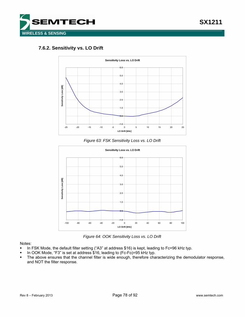
SX1211
WIRELESS & SENSING
Rev 8 – February 2013 Page 78 of 92 www.semtech.com
7.6.2. Sensitivity vs. LO Drift
Sensitivity Loss vs. LO Drift
-1.0
0.0
1.0
2.0
3.0
4.0
5.0
6.0
-25 -20 -15 -10 -5 0 5 10 15 20 25
LO Drift [kHz]
Sens
itivi
ty L
oss
[dB]
Figure 63: FSK Sensitivity Loss vs. LO Drift
Sensitivity Loss vs. LO Drift
-1.0
0.0
1.0
2.0
3.0
4.0
5.0
6.0
-100 -80 -60 -40 -20 0 20 40 60 80 100
LO Drift [kHz]
Sens
itivi
ty L
oss
[dB]
Figure 64: OOK Sensitivity Loss vs. LO Drift
Notes: In FSK Mode, the default filter setting (“A3” at address $16) is kept, leading to Fc=96 kHz typ. In OOK Mode, “F3” is set at address $16, leading to (Fc-Fo)=95 kHz typ. The above ensures that the channel filter is wide enough, therefore characterizing the demodulator response,
and NOT the filter response.

SX1211
WIRELESS & SENSING
Rev 8 – February 2013 Page 79 of 92 www.semtech.com
7.6.3. Sensitivity vs. Receiver BW
Sensitivity vs. Fc
-6.0
-5.0
-4.0
-3.0
-2.0
-1.0
0.0
1.0
50 100 150 200 250 300
Fc of Active Filter [kHz]
Sens
itivi
ty Im
prov
emen
t [dB
] =>
Figure 65: FSK Sensitivity vs. Rx BW
Sensitivity Change vs. (Fc-Fo)
-6.0
-5.0
-4.0
-3.0
-2.0
-1.0
0.0
1.0
0 50 100 150 200 250 300 350
Fc-Fo [kHz]
Sens
itivi
ty Im
prov
emen
t [dB
] =>
Figure 66: OOK Sensitivity Change vs. Rx BW
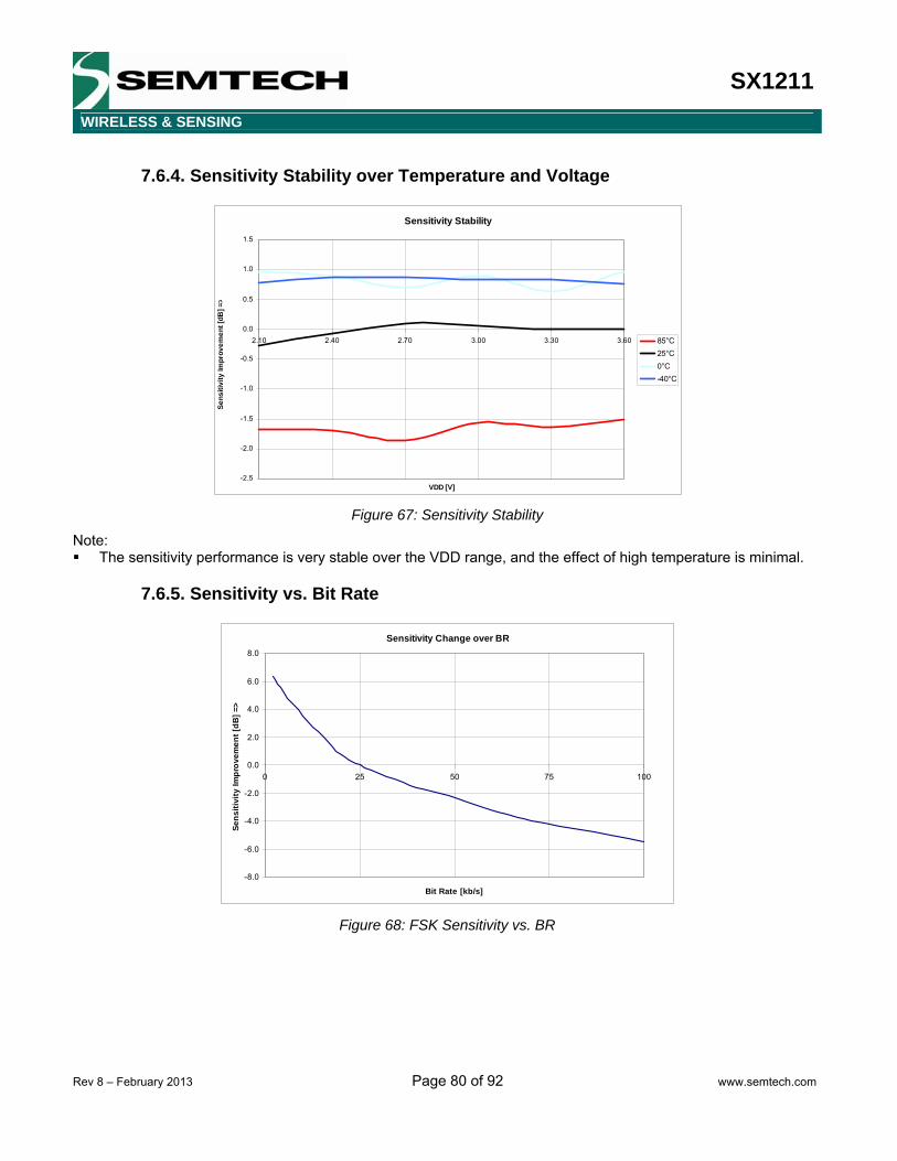
SX1211
WIRELESS & SENSING
Rev 8 – February 2013 Page 80 of 92 www.semtech.com
7.6.4. Sensitivity Stability over Temperature and Voltage
Sensitivity Stability
-2.5
-2.0
-1.5
-1.0
-0.5
0.0
0.5
1.0
1.5
2.10 2.40 2.70 3.00 3.30 3.60
VDD [V]
Sens
itivi
ty Im
prov
emen
t [dB
] =>
85°C25°C0°C-40°C
Figure 67: Sensitivity Stability
Note: The sensitivity performance is very stable over the VDD range, and the effect of high temperature is minimal.
7.6.5. Sensitivity vs. Bit Rate
Sensitivity Change over BR
-8.0
-6.0
-4.0
-2.0
0.0
2.0
4.0
6.0
8.0
0 25 50 75 100
Bit Rate [kb/s]
Sens
itivi
ty Im
prov
emen
t [dB
] =>
Figure 68: FSK Sensitivity vs. BR

SX1211
WIRELESS & SENSING
Rev 8 – February 2013 Page 81 of 92 www.semtech.com
Sensitivity Change over the BR
-2.5
-2.0
-1.5
-1.0
-0.5
0.0
0.5
1.0
1.5
2.0
1.5 4 6.5 9 11.5 14 16.5
Bit Rate [kbps]
Sens
itivi
ty Im
prov
emen
t [dB
] =>
Figure 69: OOK Sensitivity vs. BR
7.6.6. Adjacent Channel Rejection
ACR in FSK Mode
0
10
20
30
40
50
60
70
-1000 -800 -600 -400 -200 0 200 400 600 800 1000
Offset [kHz]
ACR
[dB]
Figure 70: ACR in FSK Mode
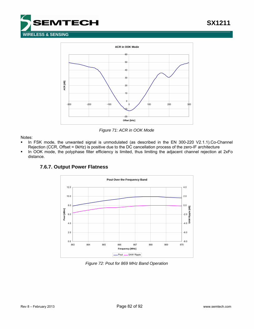
SX1211
WIRELESS & SENSING
Rev 8 – February 2013 Page 82 of 92 www.semtech.com
ACR in OOK Mode
-20
-10
0
10
20
30
40
50
60
-300 -200 -100 0 100 200 300
Offset [kHz]
ACR
[dB]
Figure 71: ACR in OOK Mode
Notes: In FSK mode, the unwanted signal is unmodulated (as described in the EN 300-220 V2.1.1).Co-Channel
Rejection (CCR, Offset = 0kHz) is positive due to the DC cancellation process of the zero-IF architecture In OOK mode, the polyphase filter efficiency is limited, thus limiting the adjacent channel rejection at 2xFo
distance.
7.6.7. Output Power Flatness
Pout Over the Frequency Band
0.0
2.0
4.0
6.0
8.0
10.0
12.0
863 864 865 866 867 868 869 870
Frequency [MHz]
Pout
[dB
m]
-8.0
-6.0
-4.0
-2.0
0.0
2.0
4.0SA
W R
ippl
e [d
B]
Pout SAW Ripple
Figure 72: Pout for 869 MHz Band Operation
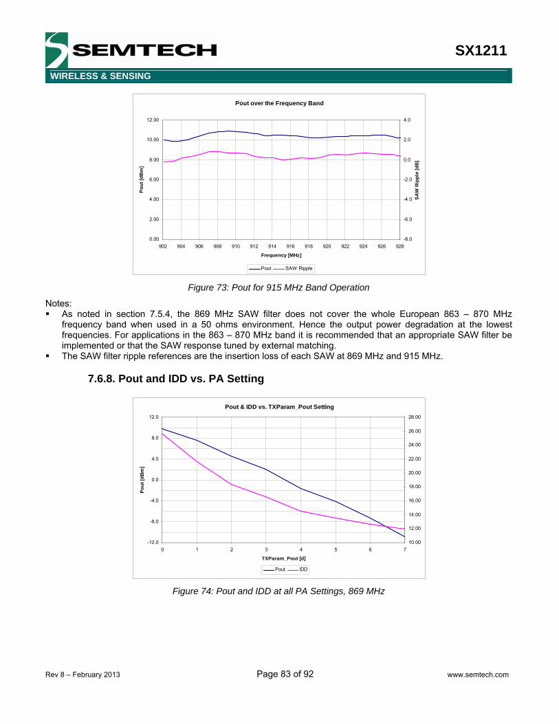
SX1211
WIRELESS & SENSING
Rev 8 – February 2013 Page 83 of 92 www.semtech.com
Pout over the Frequency Band
0.00
2.00
4.00
6.00
8.00
10.00
12.00
902 904 906 908 910 912 914 916 918 920 922 924 926 928
Frequency [MHz]
Pout
[dB
m]
-8.0
-6.0
-4.0
-2.0
0.0
2.0
4.0
SAW
Rip
ple
[dB]
Pout SAW Ripple
Figure 73: Pout for 915 MHz Band Operation
Notes: As noted in section 7.5.4, the 869 MHz SAW filter does not cover the whole European 863 – 870 MHz
frequency band when used in a 50 ohms environment. Hence the output power degradation at the lowest frequencies. For applications in the 863 – 870 MHz band it is recommended that an appropriate SAW filter be implemented or that the SAW response tuned by external matching.
The SAW filter ripple references are the insertion loss of each SAW at 869 MHz and 915 MHz.
7.6.8. Pout and IDD vs. PA Setting
Pout & IDD vs. TXParam_Pout Setting
-12.0
-8.0
-4.0
0.0
4.0
8.0
12.0
0 1 2 3 4 5 6 7
TXParam_Pout [d]
Pout
[dBm
]
10.00
12.00
14.00
16.00
18.00
20.00
22.00
24.00
26.00
28.00
Pout IDD
Figure 74: Pout and IDD at all PA Settings, 869 MHz
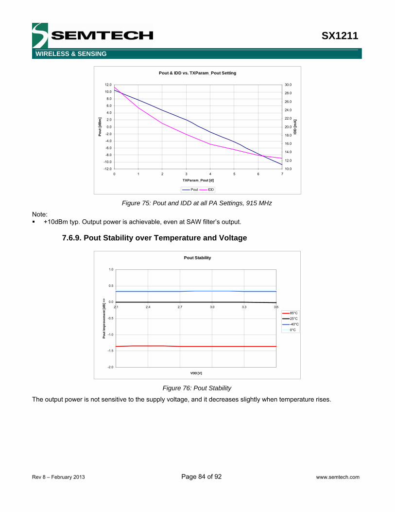
SX1211
WIRELESS & SENSING
Rev 8 – February 2013 Page 84 of 92 www.semtech.com
Pout & IDD vs. TXParam_Pout Setting
-12.0
-10.0
-8.0
-6.0
-4.0
-2.0
0.0
2.0
4.0
6.0
8.0
10.0
12.0
0 1 2 3 4 5 6 7
TXParam_Pout [d]
Pout
[dB
m]
10.0
12.0
14.0
16.0
18.0
20.0
22.0
24.0
26.0
28.0
30.0
IDD
[mA]
Pout IDD
Figure 75: Pout and IDD at all PA Settings, 915 MHz
Note: +10dBm typ. Output power is achievable, even at SAW filter’s output.
7.6.9. Pout Stability over Temperature and Voltage
Pout Stability
-2.0
-1.5
-1.0
-0.5
0.0
0.5
1.0
2.1 2.4 2.7 3.0 3.3 3.6
VDD [V]
Pout
Impr
ovem
ent [
dB] =
>
85°C25°C-40°C0°C
Figure 76: Pout Stability
The output power is not sensitive to the supply voltage, and it decreases slightly when temperature rises.

SX1211
WIRELESS & SENSING
Rev 8 – February 2013 Page 85 of 92 www.semtech.com
7.6.10. Transmitter Spectral Purity
Figure 77: 869 MHz Spectral Purity DC-1GHz
Figure 78: 869 MHz Spectral Purity 1-6GHz
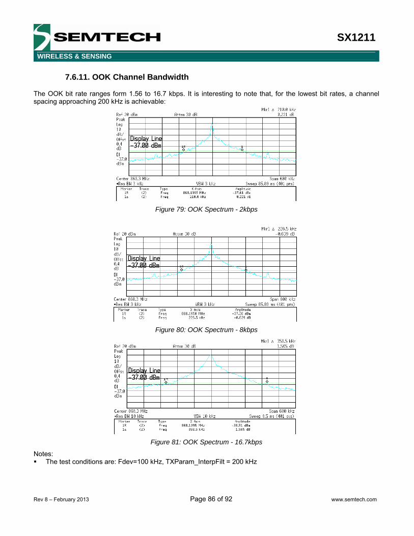
SX1211
WIRELESS & SENSING
Rev 8 – February 2013 Page 86 of 92 www.semtech.com
7.6.11. OOK Channel Bandwidth
The OOK bit rate ranges form 1.56 to 16.7 kbps. It is interesting to note that, for the lowest bit rates, a channel spacing approaching 200 kHz is achievable:
Figure 79: OOK Spectrum - 2kbps
Figure 80: OOK Spectrum - 8kbps
Figure 81: OOK Spectrum - 16.7kbps
Notes: The test conditions are: Fdev=100 kHz, TXParam_InterpFilt = 200 kHz
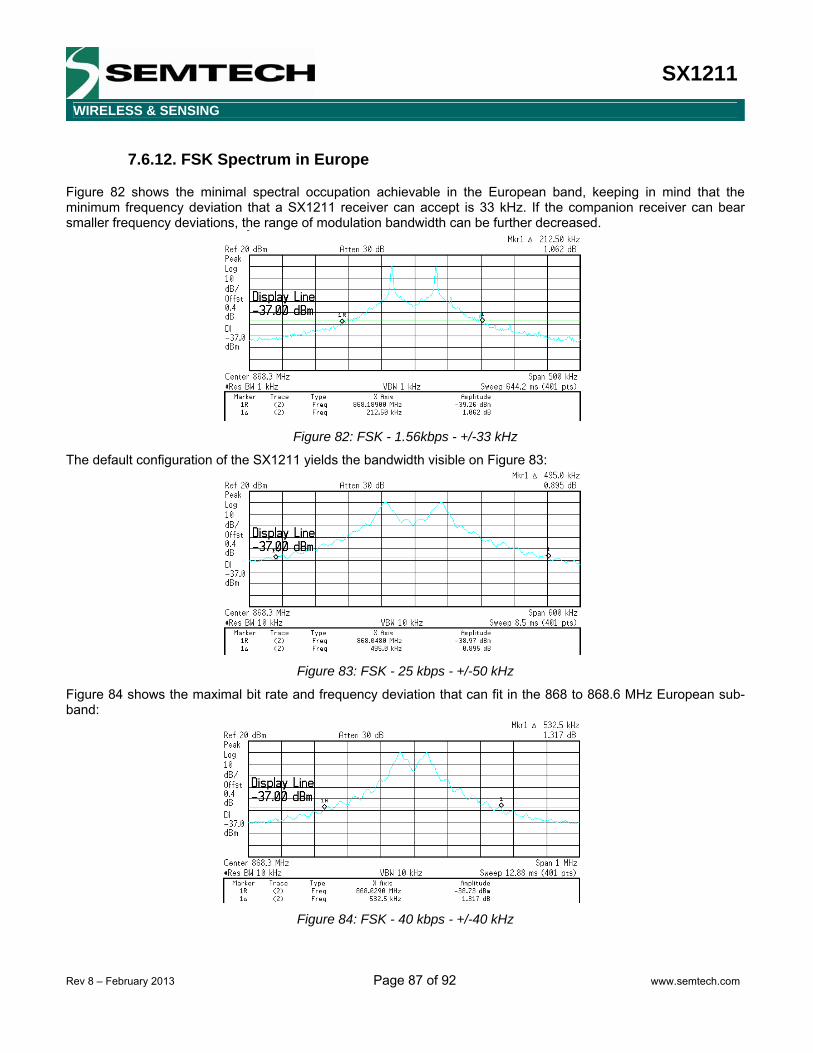
SX1211
WIRELESS & SENSING
Rev 8 – February 2013 Page 87 of 92 www.semtech.com
7.6.12. FSK Spectrum in Europe
Figure 82 shows the minimal spectral occupation achievable in the European band, keeping in mind that the minimum frequency deviation that a SX1211 receiver can accept is 33 kHz. If the companion receiver can bear smaller frequency deviations, the range of modulation bandwidth can be further decreased.
Figure 82: FSK - 1.56kbps - +/-33 kHz
The default configuration of the SX1211 yields the bandwidth visible on Figure 83:
Figure 83: FSK - 25 kbps - +/-50 kHz
Figure 84 shows the maximal bit rate and frequency deviation that can fit in the 868 to 868.6 MHz European sub-band:
Figure 84: FSK - 40 kbps - +/-40 kHz

SX1211
WIRELESS & SENSING
Rev 8 – February 2013 Page 88 of 92 www.semtech.com
7.6.13. Digital Modulation Schemes
FCC Part 15.247 allows for systems employing digital modulation techniques to transmit up to 1 W, provided that the 6 dB bandwidth of the signal is at least 500 kHz and that the power spectral density does not exceed 8dBm in any 3 kHz bandwidth. The SX1211 can actually meet these constraints whilst transmitting at the maximum output power of the device of typ. 10dBm, thanks to the built-in whitening process described in section 5.5.6.2:
Figure 85: DTS 6dB Bandwidth
Figure 86: DTS Power Spectral Density
Conditions: Pout = +10.6dBm Fdev = +/-200kHz BR=100 kbps (Chip rate=100kCps, as data whitening is enabled) Packet mode, data whitening enabled
Note: Manchester encoding allows meeting an even lower power spectral density, at the expense of the bit rate efficiency.

SX1211
WIRELESS & SENSING
Rev 8 – February 2013 Page 89 of 92 www.semtech.com
7.6.14. Current Stability over Temperature and Voltage
Tx Mode Current
(Max Output Power)
0.0
5.0
10.0
15.0
20.0
25.0
30.0
2.1 2.4 2.7 3.0 3.3 3.6
VDD [V]
Itx [m
A]
TXLV
L=00
0 85°C25°C-40°C0°C
Sleep Mode Current
0
200
400
600
800
1000
1200
2.1 2.4 2.7 3 3.3 3.6
VDD [V]
Isle
ep [n
A] 85°C25°C0°C-40°C
Standby Mode Current
0
10
20
30
40
50
60
70
80
90
100
2.1 2.4 2.7 3 3.3 3.6
VDD [V]
Istb
y [u
A] 85°C25°C0°C-40°C
FS Mode Current
0.00
0.20
0.40
0.60
0.80
1.00
1.20
1.40
1.60
1.80
2.00
2.1 2.4 2.7 3 3.3 3.6
VDD [V]
Ifs [m
A] 85°C25°C0°C-40°C
Rx Mode Current
0.00
0.50
1.00
1.50
2.00
2.50
3.00
3.50
4.00
2.1 2.4 2.7 3 3.3 3.6
VDD [V]
Irx [m
A] 85°C25°C0°C-40°C
Figure 87: IDD vs. Temp and VDD

SX1211
WIRELESS & SENSING
Rev 8 – February 2013 Page 90 of 92 www.semtech.com
8. Packaging Information
8.1. Package Outline Drawing SX1211 is available in a 32-lead TQFN package as shown in Figure 88 below.
Figure 88: Package Outline Drawing
8.2. PCB Land Pattern
Figure 89: PCB Land Pattern
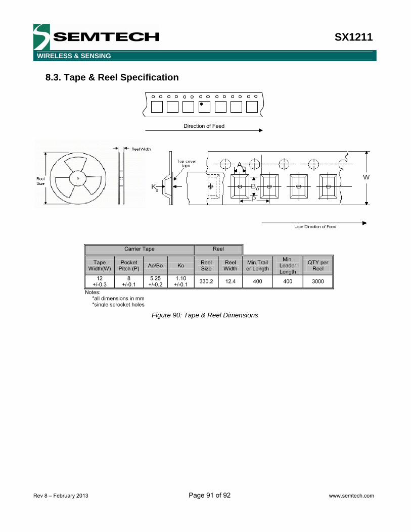
SX1211
WIRELESS & SENSING
Rev 8 – February 2013 Page 91 of 92 www.semtech.com
8.3. Tape & Reel Specification
Carrier Tape Reel
Tape Width(W)
Pocket Pitch (P) Ao/Bo Ko Reel
Size Reel Width
Min.Trailer Length
Min. Leader Length
QTY per Reel
12 +/-0.3
8 +/-0.1
5.25 +/-0.2
1.10 +/-0.1 330.2 12.4 400 400 3000
Notes: *all dimensions in mm
*single sprocket holes
Direction of Feed
Figure 90: Tape & Reel Dimensions
SX1211
WIRELESS & SENSING
Rev 8 – February 2013 Page 92 of 92 www.semtech.com
9. Revision History Revision 5 Increase maximum Bit Rate in FSK Update minimum XO frequency Add the manual reset description Insert decoupling recommendation for battery
operated systems Add Tools ordering information
Revision 6 Update SPI speed Clarify default fc value in Table 29 Clarify MISO state in SPI timing figures Improve ESD rating description
Revision 7 Describe PLL_LOCK pin state in Table 13 Improve note in section 5.4.1 Clarify Table 5 measurement conditions Clarify /Fifoempty interrupt source behavior Correct Vtune in Figure 5 Adjust VCO tuning range in section 3.2.5.2
Revision 8 Add Wafer form ordering information Update tools ordering information Update Bit Synchronizer description
10. Contact Information
© Semtech 2013 All rights reserved. Reproduction in whole or in part is prohibited without the prior written consent of the copyright owner. The information presented in this document does not form part of any quotation or contract, is believed to be accurate and reliable and may be changed without notice. No liability will be accepted by the publisher for any consequence of its use. Publication thereof does not convey nor imply any license under patent or other industrial or intellectual property rights. Semtech. assumes no responsibility or liability whatsoever for any failure or unexpected operation resulting from misuse, neglect improper installation, repair or improper handling or unusual physical or electrical stress including, but not limited to, exposure to parameters beyond the specified maximum ratings or operation outside the specified range. SEMTECH PRODUCTS ARE NOT DESIGNED, INTENDED, AUTHORIZED OR WARRANTED TO BE SUITABLE FOR USE IN LIFE-SUPPORT APPLICATIONS, DEVICES OR SYSTEMS OR OTHER CRITICAL APPLICATIONS. INCLUSION OF SEMTECH PRODUCTS IN SUCH APPLICATIONS IS UNDERSTOOD TO BE UNDERTAKEN SOLELY AT THE CUSTOMER’S OWN RISK. Should a customer purchase or use Semtech products for any such unauthorized application, the customer shall indemnify and hold Semtech and its officers, employees, subsidiaries, affiliates, and distributors harmless against all claims, costs damages and attorney fees which could arise.
Semtech Corporation Wireless and Sensing Products Division 200 Flynn Road, Camarillo, CA 93012
Phone (805) 498-2111 Fax: (805) 498-3804