
WIMAX TRANSCEIVER - University of San Diegocatcher.sandiego.edu/items/usdengr/KyoMAX_FDR_F05.pdf ·...
35
WIMAX TRANSCEIVER KYOMAX
Transcript of WIMAX TRANSCEIVER - University of San Diegocatcher.sandiego.edu/items/usdengr/KyoMAX_FDR_F05.pdf ·...

WIMAX TRANSCEIVER
KYOMAX

WiMAX Transceiver LTCC Module
Final Phase II Project Design Report Fall 2005
Submitted By:
Kyocera Group: Paula Lucchini
Nathan Roberts Marcos Vargas
Submitted To: Dr. Tom Kanneman Dr. Chuck Pateros Acknowledgements: Dr. Mikaya Lumori, USD Dr. Jerry Aguirre, Kyocera America, Inc. Tim Mobley, Dupont Jim Krasovic, Ansoft Corp. John Crow, USD
12/15/2005
ii

TABLE OF CONTENTS
EXECUTIVE SUMMARY PG. 1 INTRODUCTION PG. 2 PROBLEM STATEMENT PG. 2 MARKET AND BACKGROUND SURVEY PG. 2 TECHNICAL SURVEY PG. 4 DETAIL ON THE PROBLEM PG. 6 FUNCTIONAL REQUIREMENTS PG. 7 SPECIFICATIONS PG. 10 METHODOLOGY AND DESIGN PLAN PG. 10 TEST PLAN AND TEST RESULTS PG. 12 OUTCOMES PG. 13 CONCLUSION PG. 19 BUDGET PG. 20 PERSONNEL PG. 20 REFERENCES PG. 22 RESOURCES PG. 22 APPENDICES A. DETAILED MATERIAL PG. 23 B. GANTT CHART PG. 29 C. STUDENT RESUMES I. PAULA LUCCHINI PG.30 II. NATHAN ROBERTS PG.31 III. MARCOS VARGAS PG.32
iii

EXECUTIVE SUMMARY Wireless communication is one of the most rapidly growing industries in today’s society. Cell phones, wireless email and other recent technological inventions have led to the demand for wireless access wherever one goes. The result of this demand produced WiFi (wireless fidelity) “hotspots” in which a local company, like Starbucks, installs a wireless network to be accessed by customers while in the store. The speed and range limitations have led to a demand for newer technology to further expand the wireless market, namely WiMAX. This project focused on the development of a wireless transceiver module to be used for WiMAX applications. The module would use Kyocera America’s LTCC process and Dupont’s 943 dielectric green tape ceramic. The first phase of this project consisted of design and analysis of different module components to gain a better understanding of the electromagnetic theory involved in this high frequency microwave module. The components researched were wirebonds and via isolation techniques. Of primary importance was the discovery of an isolation phenomenon unknown to both Kyocera America and Dupont concerned with degraded isolation with the use of a via fence in between two striplines. High-end computer design and analysis tools, Ansoft HFSS and Designer, were used to design the basic structures of the module and analyze their performance. A thorough market research analysis along with technical research was pursued to develop the specifications required by the new WiMAX technology. The second phase followed with the design of the basic module components for the package based on the specifications research from phase one. A bandpass filter, a balun, a patch antenna, and a matching circuit were designed. A simulated response of all the components connected to each other was done using a black box simulation. To correlate the simulations with measurements for the via isolation project using the network analyzer, a PC board was designed and built to test the via isolation devices under test (DUT), also designed by the group and built by Dupont.
1

INTRODUCTION The goal of this project was to design a transceiver for WiMAX applications. The transceiver would be a multi-module ceramic package that would be developed after extensive market, package design and microwave engineering research. Under the guidance of Kyocera America, Inc., experts in the field of ceramic package solutions, our team, KyoMAX, would develop a plausible package for Kyocera America, Inc. to pursue in its Research and New Product Development department. WiMAX WiMAX has a theoretical range of 30 miles instead of 30 yards, with respect to WiFi, along with a stronger connection. One of the possible outcomes of WiMAX would be to place WiMAX towers in a grid much like cell phone towers and blanket an entire metropolitan area. This technology is emerging and many companies are racing to put their products first on the market. Intel Corporation is the current leader in WiMAX chip package solutions which are made using plastics. Since WiMAX currently transmits at frequencies from 2.3 GHz to 60GHz, Kyocera America believes that using ceramics instead of plastics would produce a better performing product for applications at higher frequencies (5 GHz and higher). PROBLEM STATEMENT The goal of the project is to research and design a wireless transceiver module based on basic RF components using Dupont 943 and Kyocera’s LTCC technology. The module would be applied to WiMAX technology. With the increasing market for last mile wireless access, developments must be constantly monitored for changing specifications and applications.
Figure 1: RF LTCC Multi-Chip Module
MARKET AND BACKGROUND SURVEY In the constantly developing wireless technologies that consumers utilize today, broadband wireless access is an alternative of wireless internet service providers. This is due to the unsuccessful emergence of a national broadband wireless carrier. There are only local operators providing wireless broadband services at a restricted distance and power range. This technology is establishing itself because it is attracting confidence in its potential to increase how data is transmitted wirelessly. Cost of the WiMAX technology is decreasing and bandwidth is increasing.
2

Figure 2: Sample of U.S. WiMAX Market
Due to the hype WiFi has received and the increased awareness of broadband wireless access, opportunities are becoming more available to industry. The public’s positive perception of wireless technologies has also helped in driving the development of WiMAX. There are a handful of regional players that are ready for fast growth with strong operations and management expertise in this market. Standardization of the fixed WiMAX technology is completed with equipment undergoing interoperable testing at this point in time. This technology and service is gaining ground worldwide, with major continents all investing and preparing infrastructure for WiMAX. There are a wide range of markets for this technology including construction, education, entertainment, health care, local and federal government applications, professional services such as private networks, and consumers involving media applications, video messaging, in- home multimedia and even fast internet service distributed in rural areas. The evolution of this technology is leading it to some particular roles. WiMAX will enable wireline service providers to offer broadband services in remote areas without having to build a wireline infrastructure. Also, when the technology gains support for mobility in 2007 (mobile WiMAX or 802.16e), it will allow cell carriers to offer high-speed data services. Many see WiMAX becoming a part of an inclusive service by cell carriers. Cellular companies will have their phone services using their G3 or emerging G4 techonology while using WiMAX for backhaul in data transmission and for WiFi hotspots. The market for WiMAX is $500 million today with an expected growth to $1.5 – 2 billion by the year 2007. The motivation for interest in this application was not only in its potential to change the infrastructure of data transmission and communication. The other motivation is to apply Kyocera America’s Low-Temperature Co-fired Ceramic (LTCC) process using Dupont’s Low Loss 943 Green Tape to improve WiMAX components. A benefit of LTCC SiP modules is the obvious reduction in PC board real estate. With as much as a 95% PC board real estate reduction, base stations and chipsets for the WiMAX technology could be made smaller. Therefore, the WiMAX technology would benefit from high performance at a more compact size. After extensive market research, WiMAX specifications were outlined and a frequency band of operation was chosen. Designing at
3

5.75GHz would be the best choice considering the market. At this frequency most WiMAX operation was expected due to less interference and fewer competing services (Figure 3). Kyocera America’s ceramic packages are best suited for high frequency applications. With WiMAX expected to operate at frequencies as high as 11 GHz to 60GHz, KyoMAX and Kyocera saw a potential market for its product. Furthermore, KyoMAX avoided design at the 2.3GHz and 2.5GHz bands because the market was dominated by plastic chip packages lead by Intel Corp. Plastics are not a viable solution at higher frequencies because their performance is less than a ceramic package. Thus, the 5.75 GHz band was chosen.
Figure 3: Current Frequency Ranges under Consideration
TECHNICAL SURVEY (TOOLS AND TECHNIQUES USED) Tools The project is highly oriented in computer aided design so, a major area of the project is in simulation and then tuning. The tools used by KyoMAX were Ansoft’s Designer and HFSS software. The programs were donated by Ansoft Corp. to the group for the duration of the project. Ansoft Designer is a simulation tool that links physical attributes to physical performance in a 2D design environment. HFSS is software for S-parameter and full-wave SPICE extraction and for the electromagnetic simulation of high-frequency and high-speed components. These two programs allowed for the simulation of all components of the project including the PCB board and end launch connectors. KyoMAX could design and analyze components as circuit models, planar models and 3D models. Often times each component underwent a full wave analysis using HFSS. For the design of the PCB board, ExpressPCB was used after a full wave analysis in HFSS to
4
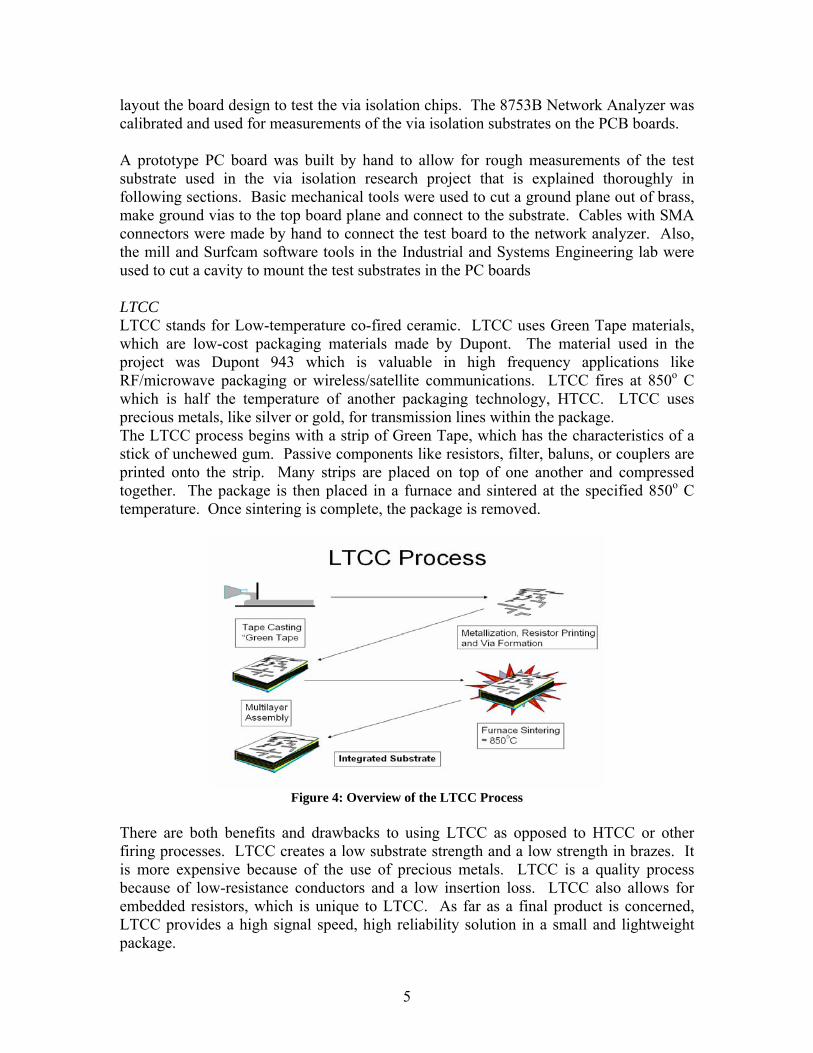
layout the board design to test the via isolation chips. The 8753B Network Analyzer was calibrated and used for measurements of the via isolation substrates on the PCB boards. A prototype PC board was built by hand to allow for rough measurements of the test substrate used in the via isolation research project that is explained thoroughly in following sections. Basic mechanical tools were used to cut a ground plane out of brass, make ground vias to the top board plane and connect to the substrate. Cables with SMA connectors were made by hand to connect the test board to the network analyzer. Also, the mill and Surfcam software tools in the Industrial and Systems Engineering lab were used to cut a cavity to mount the test substrates in the PC boards LTCC LTCC stands for Low-temperature co-fired ceramic. LTCC uses Green Tape materials, which are low-cost packaging materials made by Dupont. The material used in the project was Dupont 943 which is valuable in high frequency applications like RF/microwave packaging or wireless/satellite communications. LTCC fires at 850o C which is half the temperature of another packaging technology, HTCC. LTCC uses precious metals, like silver or gold, for transmission lines within the package. The LTCC process begins with a strip of Green Tape, which has the characteristics of a stick of unchewed gum. Passive components like resistors, filter, baluns, or couplers are printed onto the strip. Many strips are placed on top of one another and compressed together. The package is then placed in a furnace and sintered at the specified 850o C temperature. Once sintering is complete, the package is removed.
Figure 4: Overview of the LTCC Process
There are both benefits and drawbacks to using LTCC as opposed to HTCC or other firing processes. LTCC creates a low substrate strength and a low strength in brazes. It is more expensive because of the use of precious metals. LTCC is a quality process because of low-resistance conductors and a low insertion loss. LTCC also allows for embedded resistors, which is unique to LTCC. As far as a final product is concerned, LTCC provides a high signal speed, high reliability solution in a small and lightweight package.
5
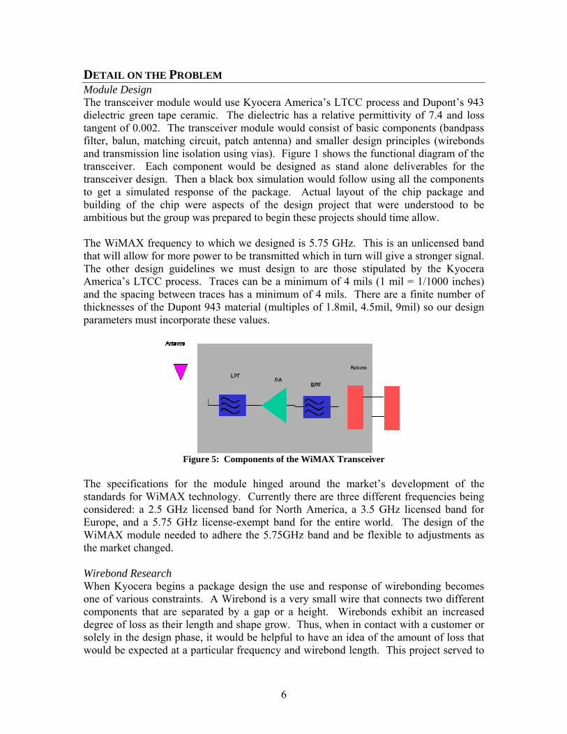
DETAIL ON THE PROBLEM Module Design The transceiver module would use Kyocera America’s LTCC process and Dupont’s 943 dielectric green tape ceramic. The dielectric has a relative permittivity of 7.4 and loss tangent of 0.002. The transceiver module would consist of basic components (bandpass filter, balun, matching circuit, patch antenna) and smaller design principles (wirebonds and transmission line isolation using vias). Figure 1 shows the functional diagram of the transceiver. Each component would be designed as stand alone deliverables for the transceiver design. Then a black box simulation would follow using all the components to get a simulated response of the package. Actual layout of the chip package and building of the chip were aspects of the design project that were understood to be ambitious but the group was prepared to begin these projects should time allow. The WiMAX frequency to which we designed is 5.75 GHz. This is an unlicensed band that will allow for more power to be transmitted which in turn will give a stronger signal. The other design guidelines we must design to are those stipulated by the Kyocera America’s LTCC process. Traces can be a minimum of 4 mils (1 mil = 1/1000 inches) and the spacing between traces has a minimum of 4 mils. There are a finite number of thicknesses of the Dupont 943 material (multiples of 1.8mil, 4.5mil, 9mil) so our design parameters must incorporate these values.
Figure 5: Components of the WiMAX Transceiver
The specifications for the module hinged around the market’s development of the standards for WiMAX technology. Currently there are three different frequencies being considered: a 2.5 GHz licensed band for North America, a 3.5 GHz licensed band for Europe, and a 5.75 GHz license-exempt band for the entire world. The design of the WiMAX module needed to adhere the 5.75GHz band and be flexible to adjustments as the market changed. Wirebond Research When Kyocera begins a package design the use and response of wirebonding becomes one of various constraints. A Wirebond is a very small wire that connects two different components that are separated by a gap or a height. Wirebonds exhibit an increased degree of loss as their length and shape grow. Thus, when in contact with a customer or solely in the design phase, it would be helpful to have an idea of the amount of loss that would be expected at a particular frequency and wirebond length. This project served to
6

quantify the response of wirebonds in terms of wirebond length and frequency. The research plan involved the variation of the gap and height of a die connected to a ceramic by a wirebond. Doing so would change the length of the wirebond. The results from the research would also aide in the WiMAX transceiver design. Via Isolation Research The via isolation project consisted of investigating the response of simulated dual striplines separated by a via fence arrangement. Due to the nature of a package being very small and the components of a package such as filters, resistors, capacitors and inductors being embedded that these components often have feed lines that are very close to each other. If one line is excited with energy it is very likely that energy will couple with a nearby dormant line. Thus, the motivation for this research arose from the general practice of placing as many vias as possible to isolate separate transmission lines, therefore improving package performance. Kyocera America’s curiosity was in how many vias was too many. If a limited or optimal number of vias could be quantified, then design rules could be developed to aid in a more cost efficient package design for Kyocera America. The data from the research would be used in the design of the WiMAX package as well. The research plan consisted of simulating striplines using three dielectric materials: Alumina, Dupont 943, and Dupont 951. This would allow for an exhaustive quantification especially of Dupont’s two materials since they are fairly new materials that Dupont desires to get more exposure and use for them. Project Constraints Throughout the project we needed to understand the computer software we were using for analysis and also needed to get simulation times under control. One potential problem that we foresaw was the timing constraint of the entire project. The project to completion was ambitious and we needed to be aware of this as we worked. We needed to be organized and it was necessary to manage our time well throughout the year and make sure that deadlines were met, especially with Kyocera and DuPont. Another potential problem was the time it took for Dupont to manufacture the via isolation substrates and for the team to design the PCB. We could not afford to wait too long for the components to arrive so we needed to be able to plan ahead and coordinate with Kyocera and DuPont to make sure we received the components as soon as possible. FUNCTIONAL REQUIREMENTS Filter: The bandpass filter required a design to the constraints of WiMAX and the LTCC process. A bandpass filter with a center frequency of 5.75 GHz and a 125 MHz bandwidth was needed. Multiple topologies were analyzed and most did not work or did not meet the size specifications for the WiMAX transceiver. The combline transformer was chosen because it could be built in a small package and was supposed to have excellent stopband performance.
7

Figure 6: HFSS model of Combline Transformer BandPass Filter
The filter was initially created using Ansoft Designer. The circuit topology was designed and it was turned into a physical circuit of resonators and capacitors. Using the physical design, the filter was then created in HFSS. Simulations were run and the filter was tuned until it was in the appropriate range for frequency and bandwidth. Balun: The purpose of a Balun is to convert between balanced and unbalanced electrical signals. Baluns isolate a transmission line and provide a balanced output. For the design of a WiMAX transceiver the balun was designed with microstrip and embedded coplanar strip lines. The Balun was developed in HFSS with WiMAX specifications and a frequency range of 4-7 GHz. The Balun design used the structural model shown in the article Wideband, Low Loss and Compact 3D LTCC Balun with Asymmetric Structure for Millimeter Wave Applications. This Balun is unique because it uses vertical coupling rather than planer coupling which helps to reduce its size.
Figure 7: 3D LTCC balun with asymmetric structure
8

The Balun Structure consists of three metal layers and two dielectric layers. The top layer contains the unbalanced input port and the second metal layer contains the balanced port. The third metal layer is a finite ground plane. Matching Circuit: A matching circuit function is to achieve maximum power transfer through impedance matching of the load and the source. For this design, the use of a wirebond transition from the ceramic to a simulated load would be used. At the input of the wirebond on the ceramic matching stubs and notches would be implemented using Smith Chart techniques obtain a 50 Ohm input impedance. Doing this will reduce power loss in the package and minimize reflections between the source and the load.
Figure 8: Matching Circuit
D943 GaAs
Antenna: An antenna is a device that converts a guided electromagnetic wave on a transmission line to a plane wave propagating in free space, or vice versa. KyoMAX’s antenna designed was a printed, bi-directional (transmit and receive), microstrip patch that would handle WiMAX frequencies. The antenna input would need impedance matching to obtain a 50 Ohm input impedance.
Figure 9: Microstrip patch antenna
9

PC Board: The PC board was a multiple step process that led to the physical hardware testing of the via isolation done in Phase I of the project. Small devices were made by Dupont to test the results of the via isolation study and these Devices Under Test (DUT) needed to be enclosed in a PC board in order to analyze them using the university’s network analyzer. The USD network analyzer has a frequency range of 1-3 GHz so we needed to design our board to operate in that range. We needed 50 Ω SMA connectors so we could connect easily to the network analyzer to get our results. The first step was to choose the proper connector. We chose the jack receptacle tabbed contact end launch connector because it met the frequency requirements and was gold plated which would help the integrity of the signal. Four connectors were ordered for each board. The next step in the PCB design was to create matching circuits for the end launch connector to PCB trace and the PCB trace to wirebond impedance mismatches. These mismatches were modeled in HFSS and analyzed using stub and notch tuners. Once both models were properly matched, we set to designing the PCB. SPECIFICATIONS The specifications for the project hinge around the market’s development of the standards for WiMAX technology. Currently there are three different frequencies being considered: a 2.5 GHz licensed band for North America, a 3.5 GHz licensed band for Europe, and a 5 GHz license-exempt band for the entire world. The design of the WiMAX module will need to adhere to these standards and be flexible as the market changes. The LTCC material to be used for the project will be Dupont 943, which comes with its own specifications. The dielectric constant is 7.4 at a frequency of 40 GHz along with a loss tangent of 0.002. The height of the material is available in multiples of 2, 5, or 10 mils thickness and the conductor thickness available in the Dupont 943 material is 0.35 mils. Also, two other materials, Alumnia and Dupont 951, were used to provide a database of material properties for this application and as a comparison of our actual material of choice. To provide an understanding of the project problem the analysis of subcomponents is required. The planned analysis looked at isolation of striplines and alternatives to providing better isolation. As mentioned earlier, the study and analysis of via fence isolation will allow us to design as compact as possible. Another design requirement is the study of wirebond transmission. Doing so provides a guideline for structure size for a desired or optimal degree of transmission. A further study looked at isolation given a bent stripline. Since the package is relatively small, transmission lines are bent and at small distances in high frequencies it is ideal to have an understanding of the coupling in such conditions. METHODOLOGY/DESIGN PLAN The design plan for the project is split into two different phases. The first phase was the analysis phase and took place during most of the first semester. This phase consisted of research into WiMAX and its market capabilities, along with learning the Ansoft
10

software EDA tools. Deeper study into microwave engineering took place during this phase along with some preliminary analysis of striplines and wirebonds to be used later during the architecture design. The analysis phase looked as follows: Phase 1: Analysis
• Market/Technical research (ongoing research to market changes) o Marcos: WiMAX industrial conference and research o Paula: WiMAX uses research o Nathan: Intel development technical research
• Learning Ansoft HFSS and Designer (in progress) • Isolation and via row characterization (to be completed in early April)
o Marcos: Analysis of DuPont 951 o Paula: Analysis of DuPont 943 o Nathan: Analysis of Alumina 473 for control purposes
• Wirebond shape inductance characterization (to begin in April) The second phase of the project took place in the Fall semester of 2005. This was the design phase of the project. We began with system component specification and component design with simulations and verifications using Ansoft HFSS. We developed some PCB board layouts to be used in hardware testing of selected components. The design phase layout looked as follows: Phase 2: Design (Semester 2)
• Balun Design o Paula: Design in HFSS for 4-7GHz
• Filter Design o Nathan: Design bandpass filter in Designer and HFSS
• Matching Circuit Design o Marcos: Design a matching circuit in HFSS
• Antenna Design o Marcos: Design Antenna in HFSS
• PC Board layout o Nathan: Design PC board layout for testing via isolation project o Paula: Check Nathan’s PCB design
• Via Isolation Measurement o Nathan: Design layout of PCB o Paula: Understand and troubleshoot Network analyzer o Marcos: Measurement validation using network analyzer
• Connect all Components o All: Physical realization o All: Pattern layout based on LTCC design rules o All: Final LTCC Module design and simulation
Once all of the components (wirebond, balun, matching circuit, filter, and stripline) were designed they were linked together in HFSS and tested to verify the functionality of the proposed transceiver. It should be noted that the project outcomes have been adjusted. The initial goal was to have a package designed and built. We understood that we might not reach that point in time since the project is very involved. To satisfy the requirement
11

of building and testing, as noted earlier, the significant research done on the via isolation project was built and verified. Thus, the adjusted deliverable is the layout of the package along with the development of a design methodology for a WiMAX transceiver module using LTCC. TEST PLAN AND TEST RESULTS The project was highly oriented in computer aided design so, a major area of the project involved simulation and then tuning. Therefore, a large part of the project consisted of testing package component prototypes. KyoMAX followed a design flow of: design, simulation (test), and tuning. Each member worked at their own pace, knowing that all the components had to be completed a few weeks before the end of the semester so the black box simulations could be analyzed. Once the components were completed, their S-parameters were recorded and exported to Designer. In Designer a circuit model was drawn, linking each component together in black box format. The results of each component were linked together and simulated. Simulating and entire 3D component in HFSS would have taken too long so the Designer method saved considerable simulation time without much loss of result quality. The other side of the project, the hardware, was in process while the components were being designed throughout the semester. The PCB had to be ready before the DUTs came back from Dupont, initially scheduled for early November. The end launch connectors and the design of the board were constructed and eventually ordered around Thanksgiving time because of a delay in the DUTs from Dupont. The boards never accepted the wirebonding well from Kyocera so make-shift wirebonding was performed by the KyoMAX team and the boards were analyzed. The true analysis will come from Kyocera’s labs since they have the equipment necessary to measure the DUTs.
Project Responsibility Due Date
Balun Design Paula 21-Nov Filter Design Nathan 21-Nov Matching Circuit Design Marcos 21-Nov Antenna Design Marcos 1-Dec PC Board Layout Design and Draw Schematic Nathan 22-Nov Validate Design using Simulation Paula 22-Nov Via Isolation Measurement Design/order PCB Nathan 23-Nov Troubleshoot Network Analyzer Paula 2-Dec
Measurement Validation Marcos 2-Dec
Connect Components Physical Realization All 1-Dec Pattern layout based on LTCC All 1-Dec Final Module Design and Simulation All 1-Dec
Table 1: Test Plan Schedule for KyoMAX
12

OUTCOMES Filter: There were some issues when designing the filter. HFSS had a difficult time converging on a solution for the filter and it never became apparent what was causing HFSS to struggle with some dimensions when other dimensions seemed to simulate quickly. One thought is that the capacitors behaved differently when placed in the dielectric.
Figure 10: Results for Bandpass Filter
The final solution for the filter resulted in a filter that met the specifications, but left room for improvement. The center frequency was a bit below 5.75 GHz and the stopband did not attenuate as much as one would like. The insertion loss at the center frequency and throughout the required bandwidth was acceptable, but the return loss could have been better. Balun: These results showed on attenuation band centered at 5GHz. The Insertion Loss is only -0.5dB which is what we wanted and the Return Loss is well below the recommended minimum of -10dB. These were excellent results for the initial design and continued adjustments were made to obtain an attenuation band centered at 5.75GHz (figure 11).
13

Figure 11: Balun Initial Results
Figure 12: Balun Final Results
As you can see from figure 12 the Return Loss is at about -35dB centered at 5.75 GHz which meets the specifications for the design. Matching Circuit: The matching circuit using the wirebond transition was matched at an input impedance of 50 Ohms.
14
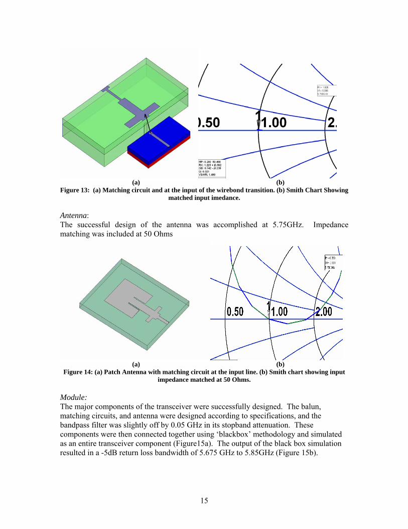
(a) (b) Figure 13: (a) Matching circuit and at the input of the wirebond transition. (b) Smith Chart Showing
matched input imedance. Antenna: The successful design of the antenna was accomplished at 5.75GHz. Impedance matching was included at 50 Ohms
(a) (b) Figure 14: (a) Patch Antenna with matching circuit at the input line. (b) Smith chart showing input
impedance matched at 50 Ohms. Module: The major components of the transceiver were successfully designed. The balun, matching circuits, and antenna were designed according to specifications, and the bandpass filter was slightly off by 0.05 GHz in its stopband attenuation. These components were then connected together using ‘blackbox’ methodology and simulated as an entire transceiver component (Figure15a). The output of the black box simulation resulted in a -5dB return loss bandwidth of 5.675 GHz to 5.85GHz (Figure 15b).
15

(a) (b)
Figure 15: (a) Black box simulation block diagram. (b) Transceiver response using black box Wirebond: The simulation steps involved the variation of the gap and height of a die connected to a ceramic by a wirebond. This project served to quantify the response of wirebonds in terms of wirebond length and frequency. The data compiled resulted in a sensitivity analysis of wirebonds showing that as wirebond length increased, insertion and return losses degraded.
Varying Gaph_p = 24 mil
-25
-20
-15
-10
-5
00 5 10 15 20 25 30 35 40
Frequency (GHz)
Ret
urn
Loss
(dB
)
-15.00
-12.00
-9.00
-6.00
-3.00
0.00
Insertion Loss (dB)
S21 5
S21 15
S21 25
S21 35
S21 45
S21 55
S21 65
S21 75
S21 85
S21 5
S21 15
S21 25
S21 35
S21 45
S21 55
S21 65
S21 75
S21 85
Varying Gaph_p = 1mil
-25
-20
-15
-10
-5
00 5 10 15 20 25 30 35 40
Frequency (GHz)
Ret
urn
Loss
(dB
)
-15.00
-12.00
-9.00
-6.00
-3.00
0.00
Insertion Loss (dB)
S11 5
S11 15
S1125
S11 35
S11 45
S11 55
S11 65
S11 75
S11 85
S21 5
S21 15
S21 25
S21 35
S21 45
S21 55
S21 65
S21 75
S21 85
Best Insertion Loss
Best Return Loss
Best Return Loss
Best Insertion Loss
(a) (b)
Figure 16: (a) Plot of wirebond response at shortest pedestal height. (b) Plot of wirebond response at a flush height. Notice that response is best when pedestal height (h_p) is flush, hence wirebond is
shortest.
16

Via Isolation: A considerable amount of data was compiled in the spring semester using Ansoft Designer’s Planar EM tool. This tool allows for the analysis of two-dimensional objects stacked in a layered arrangement. These simulations resulted in counter-intuitive results that, while via fences decrease cross-coupling at the near end (port 1 and port 2), they increase cross-coupling at the far end (port 4 and port 1). Refer to Appendix A, figures 2 and 3. Thus, in certain cases vias fences hurt more than help isolation. This conclusion goes against 30 years of general notion at Kyocera in their manufacture of multi-chip packages.
Figure 17: Via Isolation topology used for investigation. Height (H), trace gap (G) and via pitch (P)
were varied.
This outcome warranted further investigation for verification that trust in our tools had merit and also to correlate data in a full wave 3D electromagnetic analysis tool with the planar tool. Therefore, another exhaustive analysis of the dual striplines using Ansoft HFSS proceeded. Dual striplines models were simulated at three different dielectric thicknesses (18mil, 22mil, 26mil) with increasing trace spacing and different via pitches (increasing number of vias in the fence). The models were swept through frequency (1GHz to 20GHz) and focus was placed on sole use of the Dupont 943 material set. The resulting conclusion from the data correlated with the conclusion from the spring semester. HFSS showed that via fences indeed decreased cross-coupling at the near end, but increased cross coupling at the far end. A quantification of increased via pitch was assembled as well. The resulting conclusion was that the more vias (the tighter the via pitch) the worse the coupling at the far end. Refer to Appendix A, figures 4 and 5. This project has provided Kyocera with valuable insight into the designing and manufacturing practices in the company and will guide them to produce packages with less complexity in their manufacture and a reduction of time and cost. With the data complied from the via isolation project and the interest of not only Kyocera America but, also Dupont, the decision was made to build these models to test.
17

Therefore, design of the structure began at the start of this semester. Dupont first provided a probe transition to stripline prototype. The prototype consisted of a coplanar waveguide to an RF signal via transitioning down to a stripline structure. Refer to Appendix A, figure 6. The model was redrawn to allow for simulation. Alterations to the model were made for design rule compatibility and to minimize simulation complexity. The next stage involved the design of a full structure consisting of two stripline traces separated by a via fence with a total of four probe transitions at each end of each stripline. The full structure was simulated using three cases: a no via case, a via fence with 30mil via pitch case, and a via fence with 20mil via pitch case. The same phenomenon was observed with an expected increase in loss due to the various transitions. The full structure was submitted to Dupont and underwent a design rule check. Refer to Appendix A, figures 7 and 8. PCB: The small size of the DUT (0.221x0.686 inches) created a problem because the minimum trace width available on our PCB design software was too thick to have traces connect directly into the DUT. Even if we could place traces next to each other, the coupling they would induce on one another would be significant and destroy the integrity of the signal. We created traces that were 15 mils wide and angled them away from the DUT so that there was enough space to create our impedance matches while preserving the isolation of the individual traces. Even with the impedance matching, we were going to suffer loss in the small traces that were placed at an angle. To check the loss we simulated the new PCB in HFSS. We created individual traces and linked them in a black box in Designer to ease the simulation time. We saw that we had low loss in the 2 GHz range. We decided to make the board and test it at 2 GHz.
Figure 18: Completed PCB board as tested
18

The first set of boards came, but did not have proper grounding on the backs and did not have enough vias to allow Kyocera to wirebond the DUT. We took the boards and fastened a brass ground plane to the back and then drilled holes for vias. We wirebonded, by hand, the grounds of the DUT and connected to board to the network analyzer while two people connected wires to the four signal lines. Results were very mixed and we concluded that there was too much loss in the lines with our setup.
Figure 19: Network Analyzer Setup with PCB
The next step we took was to add the ground plane and the proper via holes to the board and have the boards ordered again. We got the boards and sent them to Kyocera for wirebonding. Kyocera could not wirebond to the tin/lead reflow. Wirebonding again had to be accomplished by hand. This time wirebonding was done using Kyocera’s microscopes using dry glue to create a bridge across ground to the signal port and silver paste to make the wirebonds across the bridge. This procedure was not successful due to lack of time and difficulty in placing wirebonds by hand. Kyocera, however, was able to measure the DUT’s on their network analyzer and the measurements verified our simulations: isolation at the far end was significantly reduced. Figures 9 and 10 in Appendix A show KyoMAX’s rough measurements and Kyocera’s measurements. CONCLUSION The components (balun, filter, antenna, and matching circuit) were all completed with enough time left in the semester to be able to simulate it in black box formation. Each component worked and the overall black box produced the desired result. For a complete transceiver in WiMAX communications, we would have needed to design a power amplifier and a lowpass filter. The design of these components were beyond the scope of work for this project and will be addressed by Kyocera. Kyocera will take the work done on the components and expand on them as they develop the transceiver for WiMAX.
19

The PC board encasing the DUT never produced the phenomena we were expecting to see given the via isolation analysis of Phase I. We conclude that the signal integrity loss due to the board and the problems in wirebonding influenced the results so the results are unreliable. Kyocera tested the DUTs with their sophisticated equipment and produced more reliable results that verified our simulations. The via isolation analysis turned out to be a much larger project than anticipated. Initially used as a way to familiarize ourselves with the Ansoft software and to give Kyocera a guideline for future designs, we found an unexpected phenomenon. The subject has been presented in a local Anosft industry workshop with the next goal being a presentation at IEEE electronic packaging symposium in Denver , Colorado and publishing in an IEEE journal paper. If we had more time we could have worked on the layout of the components and planned how we would layer the Dupont material for LTCC co-firing. As it is, we achieved our goal of developing a design methodology for Kyocera America and they will now take the results of our design and incorporate it into future projects. BUDGET KyoMAX was awarded a total of $850 in research grants by Associated Students. The award money was used to upgrade our computer’s RAM to aide in efficient design and simulation. Below is a budget for the full project.
Expenditures Spring 2005 -- Award Amount=$500 Item Price 4 GB of RAM (computer upgrade) $512.89 Fall 2005 -- Award Amount=$350 Item Price 2.5 GB of RAM (computer upgrade) $275.84 Documentation of Via Isolation Results $90.29
Total Awarded $850.00
Total Expenses $879.02
*The extra $29.02 was paid for by the group members.
20

PERSONNEL Company Name: KyoMAX Project Title: WiMAX Transceiver LTCC Module CEO: Marcos Vargas
Marcos Vargas will be the CEO for KyoMAX. His duties will include corresponding with professors and industry, supervising team members, and designing the matching circuit for the transceiver module.
Senior RD Engineer: Nathan Roberts Nathan Roberts will be the Senior Research and Design Engineer for KyoMAX. His duties will include aiding team members in software analysis, troubleshooting design problems, and designing the filter for the transceiver module.
Senior Project Manager: Paula Lucchini Paula Lucchini will be the Senior Project Manager for KyoMAX. Her duties will include time management, delegating assignments to team members, organizing reports and presentations, and designing the balun for the transceiver module.
21

REFERENCES Dupont. (Sept. 2003) Thick Film and Green Tape Resource Library [CD-ROM]. George E Ponchak, Donghoon Chun, Jong-Gwan Yook, Linda P.B. Katehi, “The Use of Metal Filled Via Holes for Improving Isolation in LTCC RF and Wireless Multichip Packages”, IEEE Transactions on Advanced Packaging, Vol. 23, No. 1, February 2000 Intel. (December 2004). Understanding WiMAX and 3G for Portable/Mobile Broadband Wireless. Retrieved March 14, 2005 http://www.intel.com/netcomms/technologies/downloads/305150.pdf J. Gipprich and Daniel Stevens, “A New Via Fence Structure for Crosstalk Reduction in High Density Stripline Packages”, IEEE MTT-S Digest, pp.1719-1722, 2001 Ludwig, Reinhold. RF Circuit Design: Theory and Applications, New Jersey: Prentice-Hall, 2000 Piggin, Paul. (November 2004) WiMAX In Depth. Retrieved March 14, 2005. http://www.cygnuscom.com/downloads/PN_Article.pdf Nobutaka Kidera, Stephanie Pinel, Shotaro Watanabe, Kazunari Watanabe, and Joy Laskar, “Wideband, Low Loss and Compact 3D LTCC Balun with Asymmetric Structure for Millimeter Wave Applications”, IEEE MTT-S, Long Beach 2005 Pozar, David M. Microwave Engineering, 3rd ed. New York: John Wiley & Sons, Inc., 1998 Rhea, Randall W., HF Filter Design and Computer Simulation, Georgia: Noble Publishing Company, 1994 Thomas, Nguyet Le. (Dec. 1, 2004) In the ring with WiMAX and Wi-Fi. Retrieved March 14, 2005.http://www.americasnetwork.com/americasnetwork/article/articleDetail.jsp?id=138175&pageID=1 RESOURCES MENTORS
Dr. Jerry Aguirre, Dr. Mikaya Lumori and Dr. Ernie Kim SOFTWARE
Ansoft Designer and Ansoft HFSS
22

APPENDICES A. DETAILED MATERIAL
Figure 1: Wirebond Model
Figure 2: Dual stripline model in Ansoft Designer with 3 via fences
23

S13: row comparison 20 mil pitch, 40 mil gap
-120
-100
-80
-60
-40
-20
00 5 10 15 20 25 30 35 40
Frequency (GHz)
Cou
plin
g (d
B)
no via1 row 2rowNoise Floor
Figure 3: Isolation plot in dB using Dupont 943. Note the no via case has better isolation near the
noise floor the the cases with via fences. This is the first data set using Designer in Spring 2005
Via vs. No ViaNear End Coupling (S12) -- 5.75GHz
subs. hgt=18mil
-140
-120
-100
-80
-60
-40
-20
00 5 10 15 20 25 30 35 40 45 50 55 60 65 70 75 80 85
Trace Gap (mils)
Isol
atio
n (d
B)
No Via
30mil V ia Pitch
20mil V ia Pitch
Noise Floor
Via vs. No ViaFar End Coupling (S14) -- 5.75GHz
subs. hgt=18mil
-140
-120
-100
-80
-60
-40
-20
00 5 10 15 20 25 30 35 40 45 50 55 60 65 70 75 80 85
Trace Gap (mils)
Isol
atio
n (d
B)
20mil Via Pitch
30mil Via Pitch
No Via
Noise Floor
No Via VP30
VP20
VP30
No Via
VP20
Figure 4: Far end coupling of dual striplines with via fence.
24

Varying Via PitchFar End Coupling -- 15 mil Trace Gap
-80
-70
-60
-50
-40
-30
-20
-10
010 20 30 40
Via Pitch (mil)
Isol
atio
n (d
B)
Wall NV
Varying Via PitchFar End Coupling -- Fixed at 60 mil Trace Gap
-160
-140
-120
-100
-80
-60
-40
-20
010 20 30 40
Via Pitch (mils)
Isol
atio
n (d
B)
Wall NV
Increasing Freq. Increasing
Freq.
Figure 5: Far end coupling looking at varying via pitch
Figure 6: Probe transition prototype provided by Dupont
25

Figure 7: Full structure design.
Near End Isolation -- Full Structure
-80
-70
-60
-50
-40
-30
-20
-10
00 5 10 15 20
Freq (GHz)
Isol
atio
n (d
B)
20 mil Via Pitch
30 mil Via Pitch
No Vias
Far End Isolation -- Full Structure
-70
-60
-50
-40
-30
-20
-10
00 5 10 15 20
Freq (GHz)
Isol
atio
n (d
B)
20 mil Via Pitch
30 mil Via Pitch
No Vias
No Via
No Via
VP30
VP30
VP20
VP20
(a) (b) Figure 8: Results of the simulated full DUT substrate confirmed basic simulations of the via isolation
test cases. Following these results the drawing was submitted for building to Dupont.
26

Figure 9: Rough measurements at USD. Inconclusive data based on measurements
(a) (b)
Figure 10: Kyocera America measurements of the DUT’s confirming KyoMAX simulations. There is a -15 db loss of isolation. (a) Far end coupling with no vias. (b) Far end coupling with vias (20 mil via
pitch)
27

Figure 11: Milling of PCB for DUT
Figure 12: Device Under Test (Via Isolation) in PCB
28

Figure 13: End Launch Connectors on PCB
B. PROJECT SCHEDULE:
ID Task Name
1 Simulation of full Dupontmodel
2 Research connectors3 Research board spe cs.4 Updated budget and parts lis5 CDR Report completed6 PCB boards turned in7 CDR PowerPoint8 6 weeks for Dupont parts9 Dupont parts arrive!10 Assembly11 Final Design Presentation12 FDR report Due
9/2710/20
10/2410/27
11/7
12/8
W T F S S M T W T F S S M T W T F S S M T W T F S S M T W T F S S M T W T F S S M T W T F S S M T W T F S S M T W T F S S M T W T F S S M T W T F S S M T W T F SSep 25, '05 Oct 2, '05 Oct 9, '05 Oct 16, '05 Oct 23, '05 Oct 30, '05 Nov 6, '05 Nov 13, '05 Nov 20, '05 Nov 27, '05 Dec 4, '05
29

30
Nathan Roberts 12080 NW Big Fir Circle
Portland OR 97229 Phone: 503.644.7419 Cell: 503.680.4739 Email: [email protected] Education: - University of San Diego San Diego, CA 92110 2002-Present
Major: Electrical Engineering GPA to Date: 3.68 January 2006 Minor: Mathematics Current Coursework:
- Analog Electronics: Amplifiers/Op-amps/Feedback circuits FET and BJT transistor analysis - Digital Design: VLSI design with VHDL programming
- Communications: Analog and Digital modulation/system analysis - Microprocessors: Analysis and design of 8051 processor system - Electromagnetism Analysis of electromagnetic waves and antenna construction - RF/Microwave Design Circuit design using RF/Microwave theory and principles - Computer Architecture Design, Signals and Systems, Control Systems Computer Programs: Ansoft HFSS and Designer, MatLab, Xilinx, PSpice, MathCad, Skills: Maple, Microsoft Office, Visio Web Design: Dreamweaver MX with familiarity in Fireworks MX Languages: Assembly, VHDL, familiarity in Java, C++, Perl Others: Hardware interfacing using 8051 processor Projects: - Design of transceiver module for WiMAX 2005
communications in partnership with Kyocera America using electromagnetic theory with microwave engineering principles
- Built Intel 8051-based computer system thermostat 2005 - Team leader in making (using VHDL) Direct Digital 2005
Synthesizer to plot sine/cosine waves from 10Hz to 100KHz on oscilloscope
- Designed and built a 120-watt audio amplifier using basic 2004 principles of electronics, along with computer aided design
- Led a team of four in designing a car alarm 2003 using a Z80-based processor and hardware interfacing
Work Technical Intern Intel, Hillsboro OR 2005 Experience: - Member of Microprocessor Design Team; assisted in analysis of timing circuits along with schematic corrections and data parsing (Perl scripting).
Construction Laborer: Gray Purcell, Tigard OR 2001-2003 - Assisted in building Hawthorne Living and Retail Assistant Computer Technician: Roberts’ Systems Summer 1996
- Upgraded office computer systems to current standards - Assisted in installation of new network system
Activities Senior Scholarship Award 2005 and Honors: Member of Eta Kappa Nu Honor Society - Treasurer 2004-present IEEE member 2004-present

PAULA LUCCHINI 102 E. Lewis St. [email protected] San Diego, CA 92103 (619) 920-1094 Objective To obtain a job in electrical engineering after graduating in January 2006. Education 2001- BS/BA Electrical Engineering, Mathematics minor Cumulative GPA: 3.61 University of San Diego, San Diego, CA Engineering GPA: 3.75
Expected Graduation Date: December, 2005 Honors:
• Member of The National Society of Collegiate Scholars (NSCS) since May of 2002. • Vice President of Society of Women Engineers (SWE) USD Chapter • Vice President of Eta Kappa Nu, Engineering Honors society
Qualifications and related classes Relevant Coursework
• HFSS, C++, Circuits, Electronics I and II, Material Science • 3 semesters of Physics, Microcomputers (Z80) • Engineering Economics, VHDL code • Signals and Systems, Probability and Statistics
Computer Skills • Microsoft Word, Excel, PowerPoint, LabView • some LLwin, C++, Pspice, Matlab and Maple 8.
Other Skills • organization and multitasking • personable and outgoing
Employment 6/2005-8/2005 Summer Intern, ChevronTexaco Electrical Engineering ETC/Process Automation. Software tool application using Wonderware software. 6/2004-8/2004 Summer Intern, ChevronTexaco Marketing, London, UK training in project management support to fuel strategy including assistance in implementing UK strategy and writing a complete review of European activity. 12/2003-3/2004 LabView Research, University of San Diego, San Diego, CA
Aide in writing the necessary code for interfacing the NI boards with lab equipment.
Projects o Junior year, spring 2004: Electronics II Amplifier Design Project
Design and build an audio amplifier. o Junior year, fall 2003: Microprocessor Design Project
Using knowledge of the Z80 microprocessor, designed a Z80 based car alarm using sensors, controllers, interrupts, and programmable chips.
o Sophomore year, spring 2003: Economics Project Using various cost calculations and rate of return analysis, considered five different fast food chains to invest in.
o Freshman year, spring 2002: Nifty Design Project Using the knowledge attained in an Engineering design course, made improvements on an automated car wash built by previous engineering students. Used fischertechnik components which involved a series of motors and light sensors.
o Freshman year, fall 2001: Walk on Water Project Given design specifications, team built self propelled buoyancy shoes to be used in a competition against other students. Required great organization and teamwork.
31

MARCOS ANTONIO VARGAS P.O. Box 711553, San Diego, CA 92171 (702) 858-7783 [email protected]
OBJECTIVE To obtain a position as design engineer in the RF and microwave packaging field with Kyocera America, Inc. EDUCATION University of San Diego, San Diego, CA GPA: 3.10 BS/BA in Electrical Engineering Expected: December 2005 Minor in Mathematics Relevant Coursework
• Applied Electromagnetism • RF and Microwave Engineering: Theory and Application • Power Principles • Electronic Circuits • Analytical Mechanics, Electricity, Magnetism, Optics, Modern Physics • Communications Systems Principles
Projects Served as a member of student teams comprised of 2-4 students per project
• Currently designing an RF multi-chip module for a WiMAX application utilizing Kyocera America, Inc.’s Low-Temperature Co-fired Ceramic process technology. Component design includes matching circuits, filter design, balun design, antenna design. Project requires submittal of formal documents, thorough documentation and organization of data and notes, and formal presentations.
• Conducted a full-wave analysis and characterization of via grounding techniques used to decrease electromagnetic coupling between striplines in LTCC packages. Submitted a formal report and presented to Kyocera America, Inc. and Ansoft Corp.
• Designed and built an audio amplifier with 25V power supply to output to a 100 Watt subwoofer speaker. • Improved existing design of a simulated slot machine for USD general engineering design project. Project consisted of a
computer controlled electromechanical system using Fischertechnik components. Submitted formal documents. • Designed and constructed a simple telegraph system/relay using electromagnetic principles and simple parts for physics design
project. Skills
• Modeling and Simulation in Ansoft HFSS and Ansoft Designer • Pspice, Matlab, Mathcad, Maple, Xilinx, C++ programming in Microsoft Visual Studio • Microsoft Office: Word, Excel, Powerpoint, Project, and Visio • Proficient with the Internet and constructing basic web pages • Use of Agilent 54622D Mixed Signal Oscilloscope, Agilent 33220A Function Generator, and HP 8753B Network Analyzer
WORK EXPERIENCE Kyocera America, Inc. June 2005 – August 2005 Research and Design Intern
• Aided in research of via isolation techniques and wirebond characterization. • Conducted modeling and simulation of microwave package components: balun and filter. • Conducted market research on WiMAX technology.
University of San Diego Engineering Department Fall 2003 - Present Lab Technician Assistant
• Assist Network Administrator in maintaining the department computers and network through software updates, troubleshooting and fixing problems.
• Assist professors as lab assistant and other department projects. Jenny Craig Pavilion, University of San Diego Spring 2003 – Present Ticket Sales
• Selling of tickets for USD sporting events at the Jenny Craig Pavilion Box office. • Interacting constantly with people in friendly environment and utilizing my native fluency in Spanish with customers.
AFFILIATIONS • Institute of Electrical and Electronic Engineers: USD Chapter Spring 2002 – Present
o Vice Chair Fall 2004 – Fall 2005
32

![IEEE 802.16: WiMAX Overview, WiMAX · PDF filevs. 3G. The common Misconceptions about WiMAX & 3G CDMA are [5]: 1) Cost . c. ... IEEE 802.16: WiMAX Overview, WiMAX Architecture . Mojtaba](https://static.fdocuments.us/doc/165x107/5a752f217f8b9ad22a8c6f07/ieee-80216-wimax-overview-wimax-architecture-vs-3g-the-common-misconceptions.jpg)