
William Stallings Computer Organization and Architecture 6th Edition
72
Campus de Gualtar 4710-057 Braga UNIVERSIDADE DO MINHO ESCOLA DE ENGENHARIA Departamento de Informática Computer Organization and Architecture 5th Edition, 2000 by William Stallings Summary For junior/senior/graduate-level courses in Computer Organization and Architecture in the Computer Science and Engineering departments. This text provides a clear, comprehensive presentation of the organization and architecture of modern- day computers, emphasizing both fundamental principles and the critical role of performance in driving computer design. The text conveys concepts through a wealth of concrete examples highlighting modern CISC and RISC systems. Table of Contents I. OVERVIEW . 1. Introduction. 2. Computer Evolution and Performance. II. THE COMPUTER SYSTEM. 3. System Buses . 4. Internal Memory . 5. External Memory . 6. Input/Output . 7. Operating System Support . III. THE CENTRAL PROCESSING UNIT. 8. Computer Arithmetic . 9. Instruction Sets: Characteristics and Functions. 10. Instruction Sets: Addressing Modes and Formats. 11. CPU Structure and Function . 12. Reduced Instruction Set Computers (RISCs). 13. Instruction-Level Parallelism and Superscalar Processors . IV. THE CONTROL UNIT. 14. Control Unit Operation. 15. Microprogrammed Control. V. PARALLEL ORGANIZATION. 16. Parallel Processing. Appendix A: Digital Logic. Appendix B: Projects for Teaching Computer Organization and Architecture. References. Glossary. Index. Acronyms.
-
Upload
myhomenet1191881 -
Category
Documents
-
view
112 -
download
4
description
william stallings goodbook
Transcript of William Stallings Computer Organization and Architecture 6th Edition
Campus de Gualtar 4710-057 Braga
UNIVERSIDADE DO MINHO ESCOLA DE ENGENHARIA
Departamento de Informática
Computer Organization and Architecture 5th Edition, 2000
by William Stallings
Summary
For junior/senior/graduate-level courses in Computer Organization and Architecture in the Computer Science and Engineering departments.
This text provides a clear, comprehensive presentation of the organization and architecture of modern-day computers, emphasizing both fundamental principles and the critical role of performance in driving computer design. The text conveys concepts through a wealth of concrete examples highlighting modern CISC and RISC systems.
Table of Contents
I. OVERVIEW.
1. Introduction. 2. Computer Evolution and Performance.
II. THE COMPUTER SYSTEM.
3. System Buses. 4. Internal Memory. 5. External Memory. 6. Input/Output. 7. Operating System Support.
III. THE CENTRAL PROCESSING UNIT.
8. Computer Arithmetic. 9. Instruction Sets: Characteristics and Functions. 10. Instruction Sets: Addressing Modes and Formats. 11. CPU Structure and Function. 12. Reduced Instruction Set Computers (RISCs). 13. Instruction-Level Parallelism and Superscalar Processors.
IV. THE CONTROL UNIT.
14. Control Unit Operation. 15. Microprogrammed Control.
V. PARALLEL ORGANIZATION.
16. Parallel Processing. Appendix A: Digital Logic. Appendix B: Projects for Teaching Computer Organization and Architecture. References. Glossary. Index. Acronyms.
2
Universidade do Minho – Dep. Informática - Campus de Gualtar – 4710-057 Braga - PORTUGAL- http://www.di.uminho.pt William Stallings, “Computer Organization and Architecture”, 5th Ed., 2000
Preface
OBJECTIVES
This book is about the structure and function of computers. Its purpose is to present, as clearly and completely as possible, the nature and characteristics of modern-day computer systems.
This task is challenging for several reasons. First, there is a tremendous variety of products that can rightly claim the name of "computer", from single-chip microprocessors, costing a few dollars, to supercomputers, costing tens of millions of dollars. Variety is exhibited not only in cost, but in size, performance, and application. Second, the rapid pace of change that has always characterized computer technology continues with no letup. These changes cover all aspects of computer technology, from the underlying integrated circuit technology used to construct computer components, to the increasing use of parallel organization concepts in combining those components.
In spite of the variety and pace of change in the computer field, certain fundamental concepts apply consistently throughout. The application of these concepts depends on the current state of the technology and the price/performance objectives of the designer. The intent of this book is to provide a thorough discussion of the fundamentals of computer organization and architecture and to relate these to contemporary design issues.
The subtitle suggests the theme and the approach taken in this book. It has always been important to design computer systems to achieve high performance, but never has this requirement been stronger or more difficult to satisfy than today. All of the basic performance characteristics of computer systems, including processor speed, memory speed, memory capacity, and interconnection data rates, are increasing rapidly. Moreover, they are increasing at different rates. This makes it difficult to design a balanced system that maximizes the performance and utilization of all elements. Thus, computer design increasingly becomes a game of changing the structure or function in one area to compensate for a performance mismatch in another area. We will see this game played out in numerous design decisions throughout the book.
A computer system, like any system, consists of an interrelated set of components. The system is best characterized in terms of structure-the way in which components are interconnected, and function-the operation of the individual components. Furthermore, a computer's organization is hierarchic. Each major component can be further described by decomposing it into its major subcomponents and describing their structure and function. For clarity and ease of understanding, this hierarchical organization is described in this book from the top down:
• Computer system: Major components are processor, memory, I/O.
• Processor: Major components are control unit, registers, ALU, and instruction execution unit.
• Control unit: Major components are control memory, microinstruction sequencing logic, and registers.
The objective is to present the material in a fashion that keeps new material in a clear context. This should minimize the chance that the reader will get lost and should provide better motivation than a bottom-up approach.
Throughout the discussion, aspects of the system are viewed from the points of view of both architecture (those attributes of a system visible to a machine language programmer) and organization (the operational units and their interconnections that realize the architecture).
EXAMPLE SYSTEMS
Throughout this book, examples from a number of different machines are used to clarify and reinforce the concepts being presented. Many, but by no means all, of the examples are drawn from two computer families: the Intel Pentium II, and the PowerPC. (The recently introduced Pentium III is essentially the same as the Pentium II, with an expanded set of multimedia instructions.) These two systems together encompass most of the current computer design trends. The Pentium II is essentially a complex instruction set computer (CISC) with a RISC core, while the PowerPC is essentially a reduced-instruction set computer (RISC). Both systems make use of superscalar design principles and both support multiple processor configurations.
3
Universidade do Minho – Dep. Informática - Campus de Gualtar – 4710-057 Braga - PORTUGAL- http://www.di.uminho.pt William Stallings, “Computer Organization and Architecture”, 5th Ed., 2000
PLAN OF THE TEXT
The book is organized into five parts:
Part One— Overview: This part provides a preview and context for the remainder of the book.
Part Two-The computer system: A computer system consists of processor, memory, and I/O modules, plus the interconnections among these major components. With the exception of the processor, which is sufficiently complex to be explored in Part Three, this part examines each of these aspects in turn.
Part Three— The central processing unit: The CPU consists of a control unit, registers, the arithmetic and logic unit, the instruction execution unit, and the interconnections among these components. Architectural issues, such as instruction set design and data types, are covered. The part also looks at organizational issues, such as pipelining.
Part Four— The control unit: The control unit is that part of the processor that activates the various components of the processor. This part looks at the functioning of the control unit and its implementation using microprogramming.
Part Five— Parallel organization: This final part looks at some of the issues involved in multiple processor and vector processing organizations.
A more detailed, chapter-by-chapter summary appears at the end of Chapter 1.
INTERNET SERVICES FOR INSTRUCTORS AND STUDENTS
There is a Web site for this book that provides support for students and instructors. The site includes links to other relevant sites, transparency masters of figures in the book in PDF (Adobe Acrobat) format, and sign-up information for the book's Internet mailing list. The Web page is at http://www.shore.net/~ws/COA5e.html; see the section, "Web Site for this Book," preceding this Preface, for more information. An Internet mailing list has been set up so that instructors using this book can exchange information, suggestions, and questions with each other and with the author. As soon as typos or other errors are discovered, an errata list for this book will be available at http://www.shore.net/~ws.
PROJECTS FOR TEACHING COMPUTER ORGANIZATION AND ARCHITECTURE
For many instructors, an important component of a computer organization and architecture course is a project or set of projects by which the student gets hands-on experience to reinforce concepts from the text. This book provides an unparalleled degree of support for including a projects component in the course. The instructor's manual not only includes guidance on how to assign and structure the projects, but also includes a set of suggested projects that covers a broad range of topics from the text:
• Research projects: The manual includes series of research assignments that instruct the student to research a particular topic on the Web or in the literature and write a report.
• Simulation projects: The manual provides support for the use of the simulation package SimpleScalar, which can be used to explore computer organization and architecture design issues.
• Reading/report assignments: The manual includes a list of papers in the literature, one or more for each chapter, that can be assigned for the student to read and then write a short report.
See Appendix B for details.
4
Universidade do Minho – Dep. Informática - Campus de Gualtar – 4710-057 Braga - PORTUGAL- http://www.di.uminho.pt William Stallings, “Computer Organization and Architecture”, 5th Ed., 2000
WHAT'S NEW IN THE FIFTH EDITION
In the four years since the fourth edition of this book was published, the field has seen continued innovations and improvements. In this new edition, I try to capture these changes while maintaining a broad and comprehensive coverage of the entire field. To begin this process of revision, the fourth edition of this book was extensively reviewed by a number of professors who teach the subject. The result is that, in many places, the narrative has been clarified and tightened, and illustrations have been improved. Also, a number of new "field-tested" problems have been added.
Beyond these refinements to improve pedagogy and user friendliness, there have been substantive changes throughout the book. Roughly the same chapter organization has been retained, but much of the material has been revised and new material has been added. Some of the most noteworthy changes are the following:
• Optical memory: The material on optical memory has been expanded to include magneto optical memory devices.
• Superscalar design: The chapter on superscalar design has been expanded, to include a more detailed discussion and two new examples, the U1traSparc II and the MIPS 810000.
• Multimedia instruction set: the MMX instruction set, used in the Pentium II and Pentium III, is examined.
• Predicated execution and speculative loading: This edition features a discussion of these recent concepts, which are central to the design of the new IA64 architecture from Intel and Hewlett-Packard.
• SMPs, clusters, and NUMA systems: The chapter on parallel organization has been completely rewritten. It new includes detailed descriptions of and comparisons among symmetric multiprocessors (SMPs), clusters, and nonuniform memory access (NUMA) systems.
• Expanded instructor support: As mentioned previously, the book now provides extensive support for projects. Support provided by the book Web site has also been expanded.
5
Universidade do Minho – Dep. Informática - Campus de Gualtar – 4710-057 Braga - PORTUGAL- http://www.di.uminho.pt William Stallings, “Computer Organization and Architecture”, 5th Ed., 2000
Topics from Ch. 1 to Ch. 8 and Ch.11 to Ch. 13 Text adapted from Dr. Kammerdiener slides in http://www.cs.ulm.edu/~tkammerd/spring01/csci412/lectures/, with figures from the Web site’s book publisher and from the book author’s slides (ftp://ftp.prenhall.com/pub/esm/computer_science.s-041/stallings/Slides/COA5e-Slides/); most chapters are based on the 4th ed. (see dates below, taken from Dr. Kammerdiener slides).
I. OVERVIEW. (25-Jan-99) 1. Introduction. 2. Computer Evolution and Performance.
Organization and Architecture (1.1)
• Computer Architecture refers to those attributes of a system that have a direct impact on the logical execution of a program. Examples:
o the instruction set
o the number of bits used to represent various data types
o I/O mechanisms
o memory addressing techniques
• Computer Organization refers to the operational units and their interconnections that realize the architectural specifications. Examples are things that are transparent to the programmer:
o control signals
o interfaces between computer and peripherals
o the memory technology being used
• So, for example, the fact that a multiply instruction is available is a computer architecture issue. How that multiply is implemented is a computer organization issue.
Structure and Function (1.2)
• Modern computers contain millions of electronic components
• The key to describing such systems is to recognize their hierarchical nature
o They are a set of layers or levels of interrelated subsystems
o Each level consists of a set of components and their inter-relationships
• The behavior of each level depends only on a simplified, abstracted characterization of the system at the next lower level
• At each level, the designer is concerned with:
o Structure: The way in which the components are interrelated
o Function: The operation of each individual component as part of the structure.
• We will usually describe systems from the top-down, instead of bottom-up.
Function
• A functional view of the computer
• Basic functions that a computer can perform:
o Data Processing - a wide variety of forms, but only a few fundamental methods or types
o Data Storage - long-term or short, temporary storage
6
Universidade do Minho – Dep. Informática - Campus de Gualtar – 4710-057 Braga - PORTUGAL- http://www.di.uminho.pt William Stallings, “Computer Organization and Architecture”, 5th Ed., 2000
• Data Movement
o Input/Output - when data are received from or delivered to a peripheral, a device connected directly to the computer
o Data Communications - when data is moved over longer distances, to or from a remote device
• Control - of the above functions, by instructions provided by the user of the computer (i.e. their programs)
• 4 Possible types of operations with this basic structure
Device for Processing Data in Storage Device for Processing Data En-route Between the Outside World and Storage
Structure
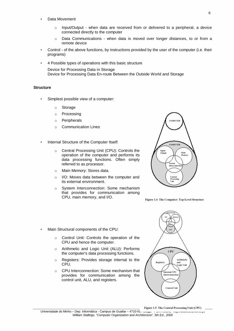
• Simplest possible view of a computer:
o Storage
o Processing
o Peripherals
o Communication Lines
• Internal Structure of the Computer Itself:
o Central Processing Unit (CPU): Controls the operation of the computer and performs its data processing functions. Often simply referred to as processor.
o Main Memory: Stores data.
o I/O: Moves data between the computer and its external environment.
o System Interconnection: Some mechanism that provides for communication among CPU, main memory, and I/O.
• Main Structural components of the CPU:
o Control Unit: Controls the operation of the CPU and hence the computer.
o Arithmetic and Logic Unit (ALU): Performs the computer's data processing functions.
o Registers: Provides storage internal to the CPU.
o CPU Interconnection: Some mechanism that provides for communication among the control unit, ALU, and registers.
7
Universidade do Minho – Dep. Informática - Campus de Gualtar – 4710-057 Braga - PORTUGAL- http://www.di.uminho.pt William Stallings, “Computer Organization and Architecture”, 5th Ed., 2000
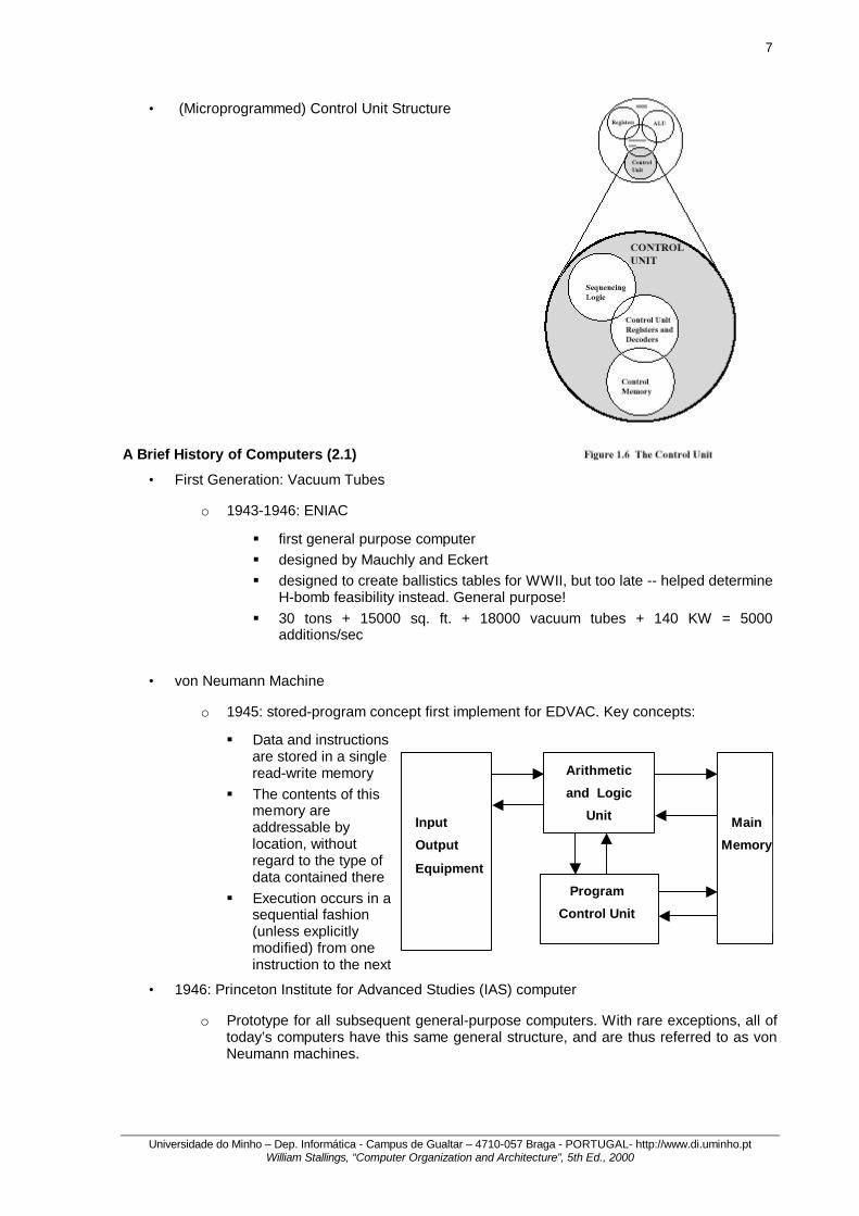
• (Microprogrammed) Control Unit Structure
A Brief History of Computers (2.1)
• First Generation: Vacuum Tubes
o 1943-1946: ENIAC
§ first general purpose computer § designed by Mauchly and Eckert § designed to create ballistics tables for WWII, but too late -- helped determine
H-bomb feasibility instead. General purpose! § 30 tons + 15000 sq. ft. + 18000 vacuum tubes + 140 KW = 5000
additions/sec
• von Neumann Machine
o 1945: stored-program concept first implement for EDVAC. Key concepts:
§ Data and instructions are stored in a single read-write memory
§ The contents of this memory are addressable by location, without regard to the type of data contained there
§ Execution occurs in a sequential fashion (unless explicitly modified) from one instruction to the next
• 1946: Princeton Institute for Advanced Studies (IAS) computer
o Prototype for all subsequent general-purpose computers. With rare exceptions, all of today’s computers have this same general structure, and are thus referred to as von Neumann machines.
Input
Output
Equipment
Arithmetic
and Logic
Unit Main
Memory
Program
Control Unit
8
Universidade do Minho – Dep. Informática - Campus de Gualtar – 4710-057 Braga - PORTUGAL- http://www.di.uminho.pt William Stallings, “Computer Organization and Architecture”, 5th Ed., 2000
• General IAS Structure Consists of:
o A main memory, which stores both data and instructions
o An ALU capable of operating on binary data
o A control unit, which interprets the instructions in memory and causes them to be executed
o I/O equipment operated by the control unit
• First commercial computers
o 1950: UNIVAC - commissioned by Census Bureau for 1950 calculations
o late 1950's: UNIVAC II § greater memory and higher performance § same basic architecture as UNIVAC § first example of upward compatibility
o 1953: IBM 701 - primarily for science
o 1955: IBM 702 - primarily for business
• Second Generation: Transistors
o 1947: Transistor developed at Bell Labs
o Introduction of more complex ALU and control units
o High-level programming languages
o Provision of system software with computers
o The data channel - an independent I/O module with its own processor and instruction set
o The multiplexor - a central termination point for data channels, CPU, and memory. Precursor to idea of data bus.
• Third Generation: Integrated Circuits
o 1958: Integrated circuit developed
o 1964: Introduction of IBM System/360 § First planned family of computer products. Characteristics of a family:
§ Similar or Identical Instruction Set and Operating System
Main Memory
Arithmetic and Logic Unit
Program Control Unit
Input Output Equipment
MBR
Arithmetic & Logic Circuits
MQ Accumulator
MAR Control Circuits
IBR
IR
PC
Address
Instructions & Data
9
Universidade do Minho – Dep. Informática - Campus de Gualtar – 4710-057 Braga - PORTUGAL- http://www.di.uminho.pt William Stallings, “Computer Organization and Architecture”, 5th Ed., 2000
§ Increasing Speed § Increasing Number of I/O Ports § Increasing Memory Size § Increasing Cost
§ Different models could all run the same software, but with different price/performance
• 1964: First PDP-8 shipped
o First minicomputer
o Started OEM market
o Introduced the bus structure
• Fourth Generation: No clear characterization
o Semiconductor memory § Replaced bulky core memory § Goes through its own generations in size, increasing by a factor of 4 each
time: 1K, 4K, 16K, 64K, 256K, 1M, 4M, 16M on a single chip w/ declining cost and access time
o Microprocessors and personal computers
o Distributed computing
o Larger and larger scales of integration Designing for Performance (2.2)
• Evolution of Computer Systems
o Price/performance § price drops every year § performance increases almost yearly § memory size goes up a factor of 4 every 3 years or so
o The basic building bocks for today's computers are the same as those of the IAS computer nearly 50 years ago
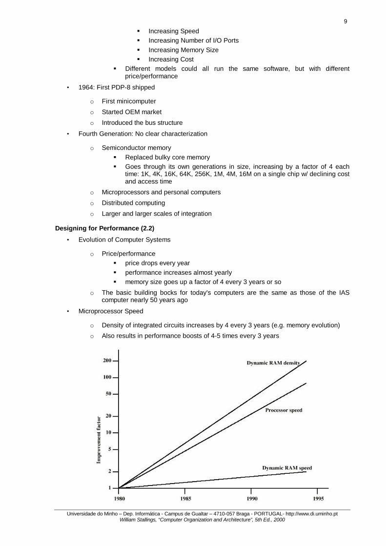
• Microprocessor Speed
o Density of integrated circuits increases by 4 every 3 years (e.g. memory evolution)
o Also results in performance boosts of 4-5 times every 3 years
10
Universidade do Minho – Dep. Informática - Campus de Gualtar – 4710-057 Braga - PORTUGAL- http://www.di.uminho.pt William Stallings, “Computer Organization and Architecture”, 5th Ed., 2000
o Requires more elaborate ways of feeding instructions quickly enough. Some techniques: § Branch prediction § Data-flow analysis § Speculative Execution
• Performance Balance
o All components do not increase performance at same rate as processor
o Results in a need to adjust the organization and architecture to compensate for the mismatch among the capabilities of the various components
• Example: Interface between processor and main memory
o Must carry a constant flow of program instructions and data between memory chips and processor
o Processor speed and memory capacity have grown rapidly
o Speed with which data can be transferred between processor and main memory has lagged badly
o DRAM density goes up faster than amount of main memory neededd § Number of DRAM's goes down § With fewer DRAM's, less opportunity for parallel data transfer
• Some solutions
o Make DRAM's "wider" to increase number of bits retrieved at once
o Change DRAM interface to make it more efficient
o Reduce frequency of memory access using increasingly complex and efficient cache structures
o Increase interconnect bandwidth with higher-speed buses and bus hierarchies
• I/O devices also become increasingly demanding
• Key is balance. Because of constant and unequal changes in:
o processor components
o main memory
o I/O devices
o interconnection structures
designers must constantly strive to balance their throughput and processing demands.
11
Universidade do Minho – Dep. Informática - Campus de Gualtar – 4710-057 Braga - PORTUGAL- http://www.di.uminho.pt William Stallings, “Computer Organization and Architecture”, 5th Ed., 2000
II. THE COMPUTER SYSTEM. 3. System Buses. (29-Jan-01) System Buses
Interconnecting Basic Components Computer Components (3.1)
• The von Neumann architecture is based on three key concepts:
o Data and instructions are stored in a single read-write memory
o The contents of this memory are addressable by location, without regard to the type of data contained there
o Execution occurs in a sequential fashion (unless explicitly modified) from one instruction to the next
• Two approaches to programming
o hardwired programming - constructing a configuration of hardware logic components to perform a particular set of arithmetic and logic operations on a set of data
o software - a sequence of codes or instructions, each of which supply the necessary control signals to a general-purpose configuration of control and logic functions (which may themselves be hardwired programs)
• Other components needed
o I/O Components - a means to: § accept data and instructions in some form, and convert to an internal form of
signals § report results
o Main memory § distinguished from external storage/peripherals § a place to temporarily store both:
§ instructions - data interpreted as codes for generating control signals § data - data upon which computations are performed
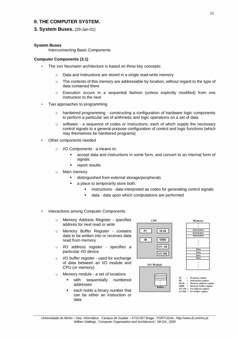
• Interactions among Computer Components
o Memory Address Register - specifies address for next read or write
o Memory Buffer Register - contains data to be written into or receives data read from memory
o I/O address register - specifies a particular I/O device
o I/O buffer register - used for exchange of data between an I/O module and CPU (or memory)
o Memory module - a set of locations § with sequentially numbered
addresses § each holds a binary number that
can be either an instruction or data
12
Universidade do Minho – Dep. Informática - Campus de Gualtar – 4710-057 Braga - PORTUGAL- http://www.di.uminho.pt William Stallings, “Computer Organization and Architecture”, 5th Ed., 2000
Computer Function (3.2)
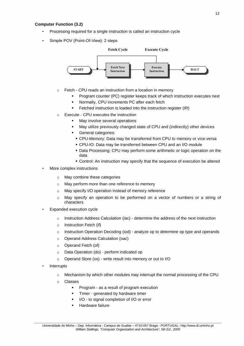
• Processing required for a single instruction is called an instruction cycle
• Simple POV (Point-Of-View): 2 steps
o Fetch - CPU reads an instruction from a location in memory § Program counter (PC) register keeps track of which instruction executes next § Normally, CPU increments PC after each fetch § Fetched instruction is loaded into the instruction register (IR)
o Execute - CPU executes the instruction § May involve several operations § May utilize previously changed state of CPU and (indirectly) other devices § General categories: § CPU-Memory: Data may be transferred from CPU to memory or vice-versa § CPU-IO: Data may be transferred between CPU and an I/O module § Data Processing: CPU may perform some arithmetic or logic operation on the
data § Control: An instruction may specify that the sequence of execution be altered
• More complex instructions
o May combine these categories
o May perform more than one reference to memory
o May specify I/O operation instead of memory reference
o May specify an operation to be performed on a vector of numbers or a string of characters
• Expanded execution cycle
o Instruction Address Calculation (iac) - determine the address of the next instruction
o Instruction Fetch (if)
o Instruction Operation Decoding (iod) - analyze op to determine op type and operands
o Operand Address Calculation (oac)
o Operand Fetch (of)
o Data Operation (do) - perform indicated op
o Operand Store (os) - write result into memory or out to I/O
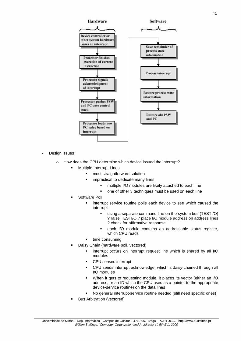
• Interrupts
o Mechanism by which other modules may interrupt the normal processing of the CPU
o Classes § Program - as a result of program execution § Timer - generated by hardware timer § I/O - to signal completion of I/O or error § Hardware failure
13
Universidade do Minho – Dep. Informática - Campus de Gualtar – 4710-057 Braga - PORTUGAL- http://www.di.uminho.pt William Stallings, “Computer Organization and Architecture”, 5th Ed., 2000
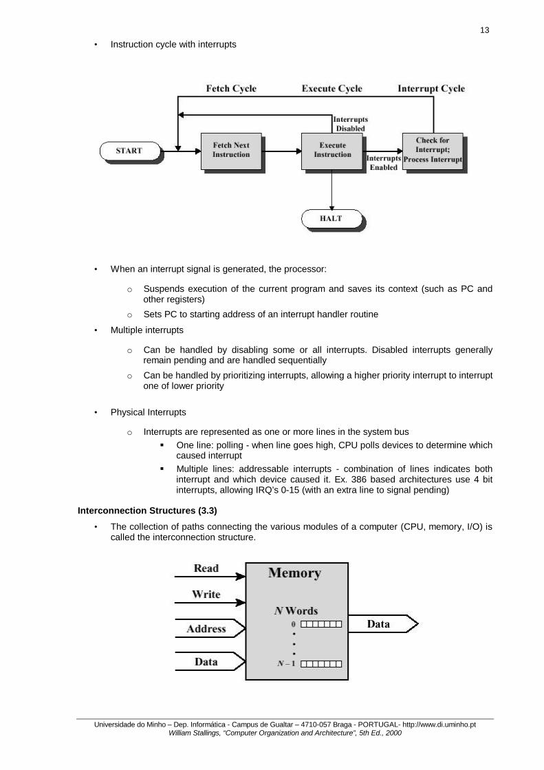
• Instruction cycle with interrupts
• When an interrupt signal is generated, the processor:
o Suspends execution of the current program and saves its context (such as PC and other registers)
o Sets PC to starting address of an interrupt handler routine
• Multiple interrupts
o Can be handled by disabling some or all interrupts. Disabled interrupts generally remain pending and are handled sequentially
o Can be handled by prioritizing interrupts, allowing a higher priority interrupt to interrupt one of lower priority
• Physical Interrupts
o Interrupts are represented as one or more lines in the system bus § One line: polling - when line goes high, CPU polls devices to determine which
caused interrupt § Multiple lines: addressable interrupts - combination of lines indicates both
interrupt and which device caused it. Ex. 386 based architectures use 4 bit interrupts, allowing IRQ’s 0-15 (with an extra line to signal pending)
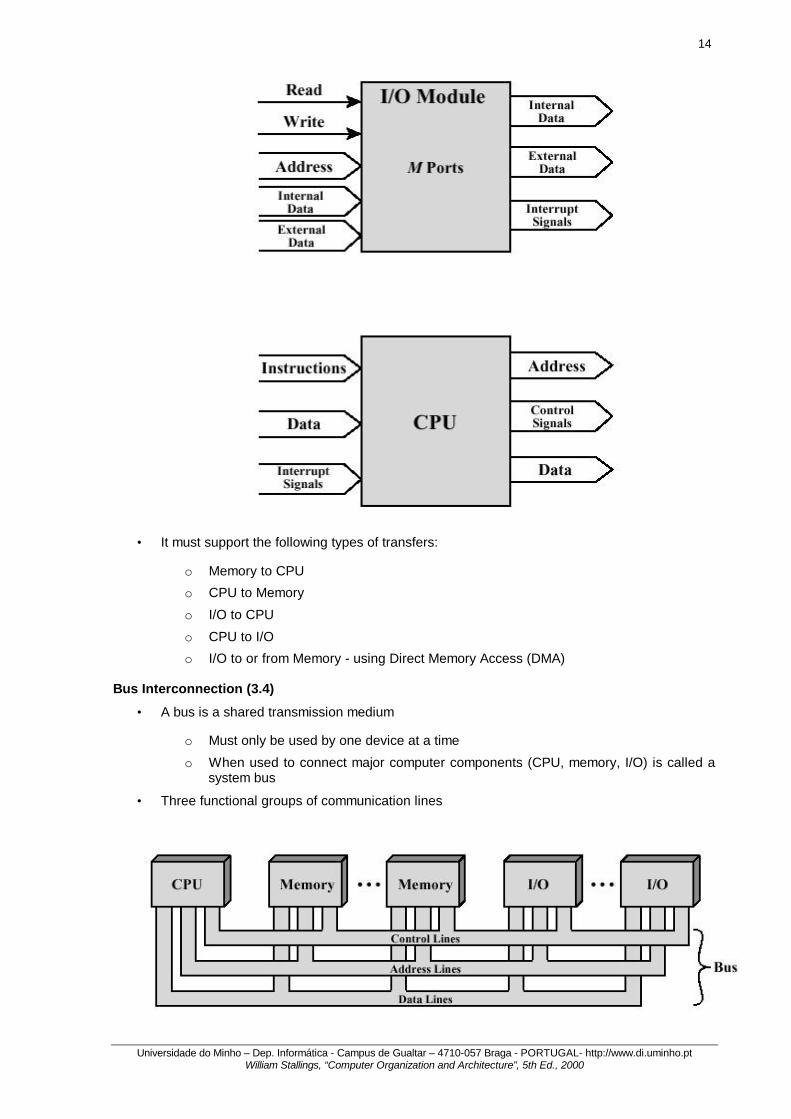
Interconnection Structures (3.3)
• The collection of paths connecting the various modules of a computer (CPU, memory, I/O) is called the interconnection structure.
14
Universidade do Minho – Dep. Informática - Campus de Gualtar – 4710-057 Braga - PORTUGAL- http://www.di.uminho.pt William Stallings, “Computer Organization and Architecture”, 5th Ed., 2000
• It must support the following types of transfers:
o Memory to CPU
o CPU to Memory
o I/O to CPU
o CPU to I/O
o I/O to or from Memory - using Direct Memory Access (DMA) Bus Interconnection (3.4)
• A bus is a shared transmission medium
o Must only be used by one device at a time
o When used to connect major computer components (CPU, memory, I/O) is called a system bus
• Three functional groups of communication lines
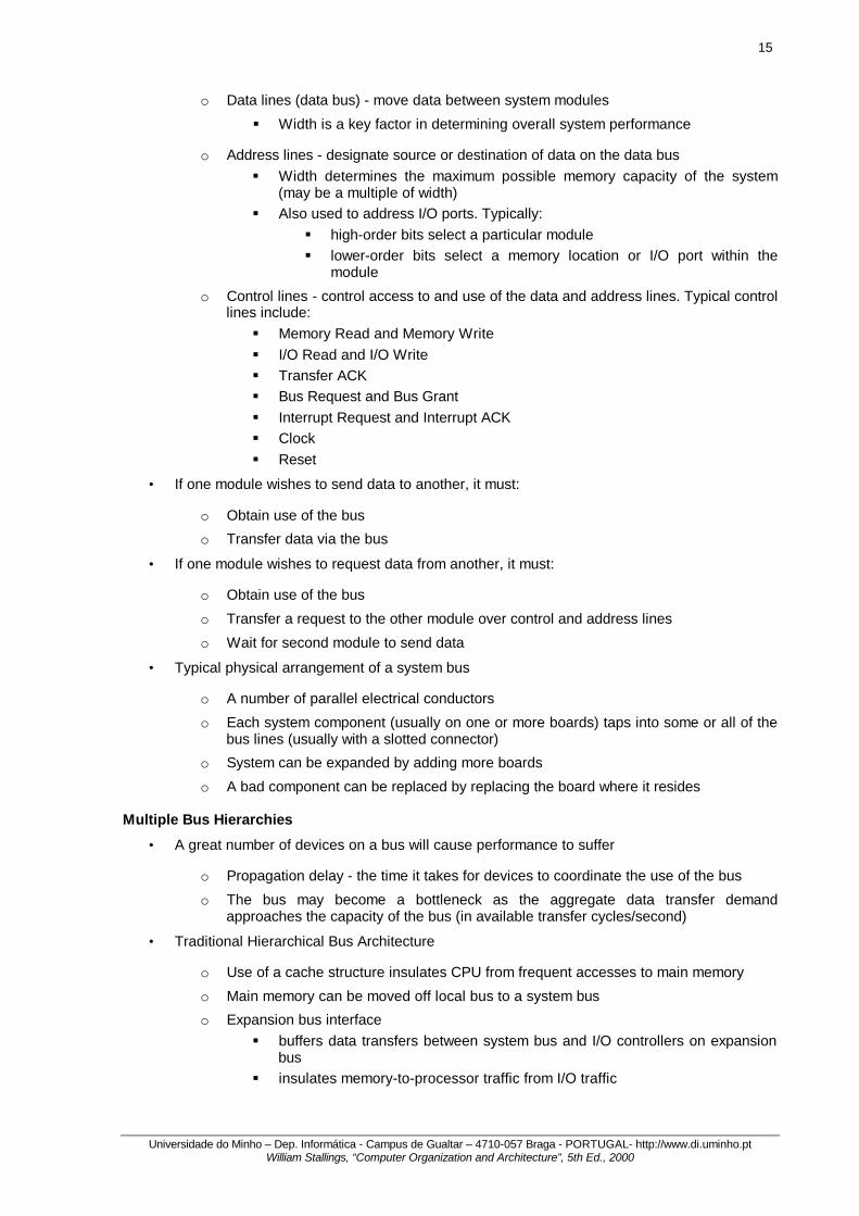
15
Universidade do Minho – Dep. Informática - Campus de Gualtar – 4710-057 Braga - PORTUGAL- http://www.di.uminho.pt William Stallings, “Computer Organization and Architecture”, 5th Ed., 2000
o Data lines (data bus) - move data between system modules
§ Width is a key factor in determining overall system performance
o Address lines - designate source or destination of data on the data bus § Width determines the maximum possible memory capacity of the system
(may be a multiple of width) § Also used to address I/O ports. Typically:
§ high-order bits select a particular module § lower-order bits select a memory location or I/O port within the
module
o Control lines - control access to and use of the data and address lines. Typical control lines include: § Memory Read and Memory Write § I/O Read and I/O Write § Transfer ACK § Bus Request and Bus Grant § Interrupt Request and Interrupt ACK § Clock § Reset
• If one module wishes to send data to another, it must:
o Obtain use of the bus
o Transfer data via the bus
• If one module wishes to request data from another, it must:
o Obtain use of the bus
o Transfer a request to the other module over control and address lines
o Wait for second module to send data
• Typical physical arrangement of a system bus
o A number of parallel electrical conductors
o Each system component (usually on one or more boards) taps into some or all of the bus lines (usually with a slotted connector)
o System can be expanded by adding more boards
o A bad component can be replaced by replacing the board where it resides Multiple Bus Hierarchies
• A great number of devices on a bus will cause performance to suffer
o Propagation delay - the time it takes for devices to coordinate the use of the bus
o The bus may become a bottleneck as the aggregate data transfer demand approaches the capacity of the bus (in available transfer cycles/second)
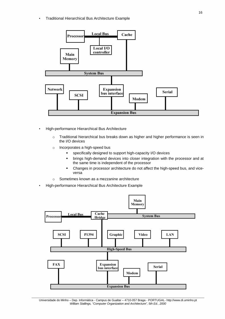
• Traditional Hierarchical Bus Architecture
o Use of a cache structure insulates CPU from frequent accesses to main memory
o Main memory can be moved off local bus to a system bus
o Expansion bus interface § buffers data transfers between system bus and I/O controllers on expansion
bus § insulates memory-to-processor traffic from I/O traffic
16
Universidade do Minho – Dep. Informática - Campus de Gualtar – 4710-057 Braga - PORTUGAL- http://www.di.uminho.pt William Stallings, “Computer Organization and Architecture”, 5th Ed., 2000
• Traditional Hierarchical Bus Architecture Example
• High-performance Hierarchical Bus Architecture
o Traditional hierarchical bus breaks down as higher and higher performance is seen in the I/O devices
o Incorporates a high-speed bus § specifically designed to support high-capacity I/O devices § brings high-demand devices into closer integration with the processor and at
the same time is independent of the processor § Changes in processor architecture do not affect the high-speed bus, and vice-
versa
o Sometimes known as a mezzanine architecture
• High-performance Hierarchical Bus Architecture Example
17
Universidade do Minho – Dep. Informática - Campus de Gualtar – 4710-057 Braga - PORTUGAL- http://www.di.uminho.pt William Stallings, “Computer Organization and Architecture”, 5th Ed., 2000
Elements of Bus Design
• Bus Types
o Dedicated - a line is permanently assigned either to one function or to a physical subset of computer components
o Multiplexed § Time multiplexing - using the same lines for multiple purposes (different
purposes at different times) § Uses fewer lines, saving space and cost § BUT more complex circuitry required in each module § BUT potential reduction in performance
• Physical dedication - the use of multiple buses, each of which connects to only a subset of modules, with an adapter module to connect buses and resolve contention at the higher level
• Method of Arbitration - determining who can use the bus at a particular time
o Centralized - a single hardware device called the bus controller or arbiter allocates time on the bus
o Distributed - each module contains access control logic and the modules act together to share the bus
o Both methods designate one device (either CPU or an I/O module) as master, which may initiate a data transfer with some other device, which acts as a slave.
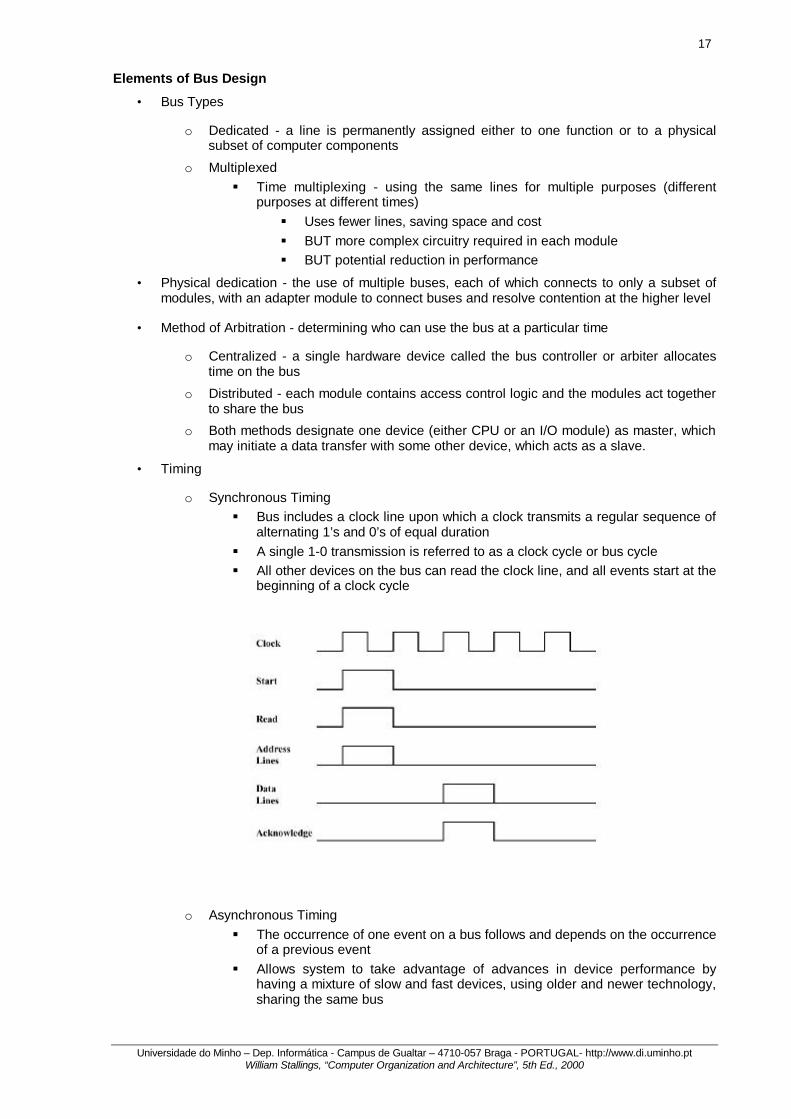
• Timing
o Synchronous Timing § Bus includes a clock line upon which a clock transmits a regular sequence of
alternating 1’s and 0’s of equal duration § A single 1-0 transmission is referred to as a clock cycle or bus cycle § All other devices on the bus can read the clock line, and all events start at the
beginning of a clock cycle
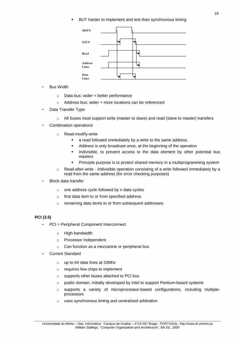
o Asynchronous Timing § The occurrence of one event on a bus follows and depends on the occurrence
of a previous event § Allows system to take advantage of advances in device performance by
having a mixture of slow and fast devices, using older and newer technology, sharing the same bus
18
Universidade do Minho – Dep. Informática - Campus de Gualtar – 4710-057 Braga - PORTUGAL- http://www.di.uminho.pt William Stallings, “Computer Organization and Architecture”, 5th Ed., 2000
§ BUT harder to implement and test than synchronous timing
• Bus Width
o Data bus: wider = better performance
o Address bus: wider = more locations can be referenced
• Data Transfer Type
o All buses must support write (master to slave) and read (slave to master) transfers
• Combination operations
o Read-modify-write § a read followed immediately by a write to the same address. § Address is only broadcast once, at the beginning of the operation § Indivisible, to prevent access to the data element by other potential bus
masters § Principle purpose is to protect shared memory in a multiprogramming system
o Read-after-write - indivisible operation consisting of a write followed immediately by a read from the same address (for error checking purposes)
• Block data transfer
o one address cycle followed by n data cycles
o first data item to or from specified address
o remaining data items to or from subsequent addresses PCI (3.5)
• PCI = Peripheral Component Interconnect
o High-bandwidth
o Processor independent
o Can function as a mezzanine or peripheral bus
• Current Standard
o up to 64 data lines at 33Mhz
o requires few chips to implement
o supports other buses attached to PCI bus
o public domain, initially developed by Intel to support Pentium-based systems
o supports a variety of microprocessor-based configurations, including multiple-processors
o uses synchronous timing and centralized arbitration
19
Universidade do Minho – Dep. Informática - Campus de Gualtar – 4710-057 Braga - PORTUGAL- http://www.di.uminho.pt William Stallings, “Computer Organization and Architecture”, 5th Ed., 2000
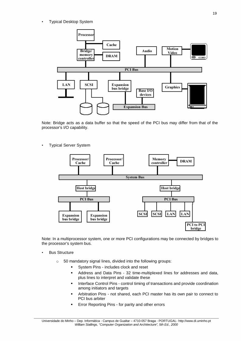
• Typical Desktop System
Note: Bridge acts as a data buffer so that the speed of the PCI bus may differ from that of the processor’s I/O capability.
• Typical Server System
Note: In a multiprocessor system, one or more PCI configurations may be connected by bridges to the processor’s system bus.
• Bus Structure
o 50 mandatory signal lines, divided into the following groups: § System Pins - includes clock and reset § Address and Data Pins - 32 time-multiplexed lines for addresses and data,
plus lines to interpret and validate these § Interface Control Pins - control timing of transactions and provide coordination
among initiators and targets § Arbitration Pins - not shared, each PCI master has its own pair to connect to
PCI bus arbiter § Error Reporting Pins - for parity and other errors
20
Universidade do Minho – Dep. Informática - Campus de Gualtar – 4710-057 Braga - PORTUGAL- http://www.di.uminho.pt William Stallings, “Computer Organization and Architecture”, 5th Ed., 2000
o 50 optional signal lines, divided into the following groups: § Interrupt Pins - not shared, each PCI device has its own interrupt line or lines
to an interrupt controller § Cache Support Pins § 64-bit Bus Extension Pins - 32 additional time-multiplexed lines for addresses
and data, plus lines to interpret and validate these, and to provide agreement between two PCI devices on use of these
§ ITAG/Boundary Scan Pins - support testing procedures from IEEE Standard 149.1
• PCI Commands
o issued by the initiator (the master) to the target (the slave)
o Use the C/BE lines
o Types
- Interrupt Ack - Memory Read Multiple - Special Cycle - Memory Write - I/O Read - Memory Write & Invalidate - I/O Write - Configuration Read - Memory Read - Configuration Write - Memory Read Line - Dual Address Cycle
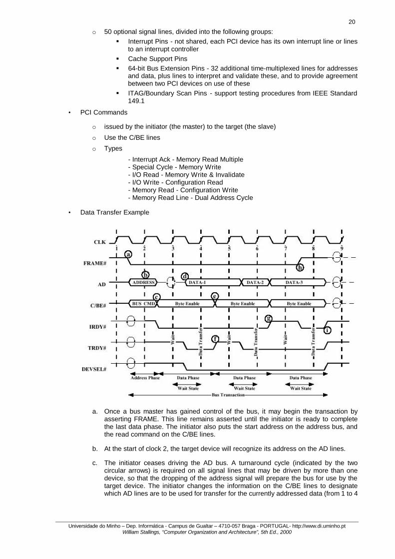
• Data Transfer Example
a. Once a bus master has gained control of the bus, it may begin the transaction by asserting FRAME. This line remains asserted until the initiator is ready to complete the last data phase. The initiator also puts the start address on the address bus, and the read command on the C/BE lines.
b. At the start of clock 2, the target device will recognize its address on the AD lines.
c. The initiator ceases driving the AD bus. A turnaround cycle (indicated by the two circular arrows) is required on all signal lines that may be driven by more than one device, so that the dropping of the address signal will prepare the bus for use by the target device. The initiator changes the information on the C/BE lines to designate which AD lines are to be used for transfer for the currently addressed data (from 1 to 4
21
Universidade do Minho – Dep. Informática - Campus de Gualtar – 4710-057 Braga - PORTUGAL- http://www.di.uminho.pt William Stallings, “Computer Organization and Architecture”, 5th Ed., 2000
bytes). The initiator also asserts IRDY to indicated that it is ready for the first data item.
d. The selected target asserts DEVSEL to indicate that it has recognized its address and will respond. It places the requested data on the AD lines and asserts TRDY to indicate that valid data is present on the bus.
e. The initiator reads the data at the beginning of clock 4 and changes the byte enable lines as needed in preparation for the next read.
f. In this example, the target needs some time to prepare the second block of data for transmission. Therefore, it deasserts TRDY to signal the initiator that there will not be new data during the coming cycle. Accordingly, the initiator does not read the data lines at the beginning of the 5th clock cycle and does not change byte enable during that cycle. The block of data is read at beginning of clock 6.
g. During clock 6, the target places the 3rd data item on the bus. However, in this example, the initiator is not yet ready to read the data item (e.g., it has a temporary buffer full condition). It therefore deasserts IRDY. This will cause the target to maintain the third data item on the bus for an extra clock cycle.
h. The initiator knows that the 3rd data transfer is the last, and so it deasserts FRAME to signal the target that this is the last data transfer. It also asserts IRDY to signal that it is ready to complete that transfer.
i. The initiator deasserts IRDY, returning the bus to the idle state, and the target deasserts TRDY and DEVSEL.
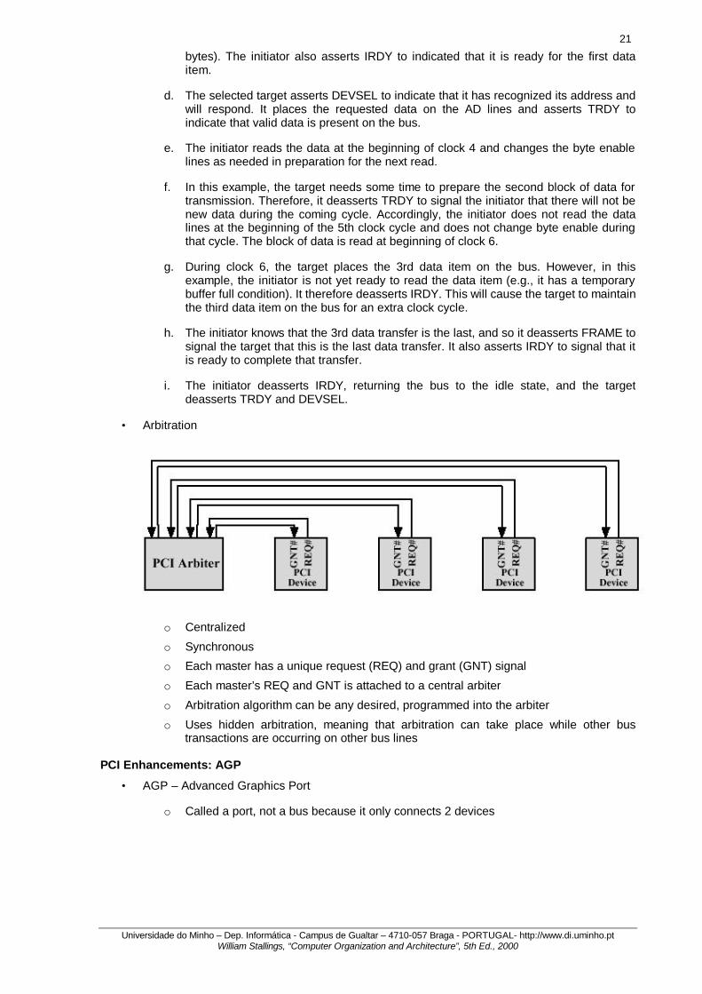
• Arbitration
o Centralized
o Synchronous
o Each master has a unique request (REQ) and grant (GNT) signal
o Each master’s REQ and GNT is attached to a central arbiter
o Arbitration algorithm can be any desired, programmed into the arbiter
o Uses hidden arbitration, meaning that arbitration can take place while other bus transactions are occurring on other bus lines
PCI Enhancements: AGP
• AGP – Advanced Graphics Port
o Called a port, not a bus because it only connects 2 devices
22
Universidade do Minho – Dep. Informática - Campus de Gualtar – 4710-057 Braga - PORTUGAL- http://www.di.uminho.pt William Stallings, “Computer Organization and Architecture”, 5th Ed., 2000
II. THE COMPUTER SYSTEM. 3. ... 4. Internal Memory. (29-Feb-00) Characteristics of Computer Memory Systems (4.1)
• Location
o CPU (registers and L1 cache)
o Internal Memory (main)
o External (secondary)
• Capacity
o Word Size - typically equal to the number of bits used to represent a number and to the instruction length.
o Number of Words - has to do with the number of addressable units (which are typically words, but are sometimes bytes, regardless of word size). For addresses of length A (in bits), the number of addressable units is 2A.
• Unit of Transfer
o Word
o Block
• Access Method
o Sequential Access § information used to separate or identify records is stored with the records § access must be made in a specific linear sequence § the time to access an arbitrary record is highly variable
o Direct Access § individual blocks or records have an address based on physical location § access is by direct access to general vicinity of desired information, then
some search § access time is still variable, but not as much as sequential access
o Random Access § each addressable location has a unique, physical location § access is by direct access to desired location § access time is constant and independent of prior accesses
o Associative § desired units of information are retrieved by comparing a sub-part of the unit
with a desired mask -- location is not needed § all matches to the mask are retrieved simultaneously § access time is constant and independent of prior accesses § most useful for searching - a search through N possible locations would take
O(N) with Random Access Memory, but O(1) with Associative Memory
• Performance
o Access Time
o Memory Cycle Time - primarily for random-access memory = access time + additional time required before a second access can begin (refresh time, for example)
o Transfer Rate § Generally measured in bits/second
23
Universidade do Minho – Dep. Informática - Campus de Gualtar – 4710-057 Braga - PORTUGAL- http://www.di.uminho.pt William Stallings, “Computer Organization and Architecture”, 5th Ed., 2000
§ Inversely proportional to memory cycle time for random access memory
• Physical Type
o Most common - semiconductor and magnetic surface memories
o Others - optical, bubble, mechanical (e.g. paper tape), core, esoteric/theoretical (e.g. biological)
• Physical Characteristics
o volatile - information decays or is lost when power is lost
o non-volatile - information remains without deterioration until changed -- no electrical power needed
o non-erasable § information cannot be altered with a normal memory access cycle § As a practical matter, must be non-volatile
• Organization - the physical arrangement of bits to form words.
o Obvious arrangement not always used
o Ex. Characters vs. Integers vs. Floating Point Numbers The Memory Hierarchy
• Design Constraints
o How much? “If you build it, they will come.” Applications tend to be built to use any commonly available amount, so question is open-ended.
o How fast? Must be able to keep up with the CPU -- don’t want to waste cycles waiting for instructions or operands.
o How expensive? Cost of memory (also associated with “How much?”) must be reasonable vs. other component costs.
• There are trade-offs between the 3 key characteristics of memory (cost, capacity, and access time) which yield the following relationships:
o Smaller access time -> greater cost per bit o Greater capacity -> smaller cost per bit o Greater capacity -> greater access time
• The designer’s dilemma
o Would like to use cheaper, large capacity memory technologies o Good performance requires expensive, lower-capacity, quick-access memories
• Solution: Don’t rely on a single memory component or technology -- use a memory hierarchy
o Organizes memories such that: § Cost/bit decreases § Capacity increases § Access time increases
o Data and instructions are distributed across this memory according to: § Frequency of access of the memory by the CPU decreases (key to success)
o This scheme will reduced overall costs while maintaining a given level of performance.
• Contemporary Memory Hierarchy
Magnetic Tape Optical/Magnetic Disk Disk Cache Main Memory Cache Registers
24
Universidade do Minho – Dep. Informática - Campus de Gualtar – 4710-057 Braga - PORTUGAL- http://www.di.uminho.pt William Stallings, “Computer Organization and Architecture”, 5th Ed., 2000
• Success depends upon the locality of reference principle
o memory references tend to cluster § temporal locality - if a location is referenced, it is likely to be referenced again
in the near future § positional locality - when a location is referenced, it is probably close to the
last location referenced
o so a single (slower) transfer of memory from a lower level of the hierarchy to a higher level of the hierarchy will tend to service a disproportionate number of future requests, which can be satisfied by the higher (faster) level
o This is the technique which is the basis for caching and virtual memory
o Although we don’t always refer to it as caching, this technique is used at all levels of the memory hierarchy, often supported at the operating system level
Semiconductor Main Memory (4.2)
• Types of Random-Access Semiconductor Memory
o RAM - Random Access Memory § misused term (all these are random access) § possible both to read data from the memory and to easily and rapidly write
new data into the memory § volatile - can only be used for temporary storage (all the other types of
random-access memory are non-volatile) § types:
§ dynamic - stores data as charge on capacitors § tend to discharge over time § require periodic charge (like a memory reference) to refresh § more dense and less expensive than comparable static
RAMs § static - stores data in traditional flip-flop logic gates
§ no refresh needed § generally faster than dynamic RAMs
o ROM - Read Only Memory § contains a permanent pattern of data which cannot be changed § data is actually wired-in to the chip as part of the fabrication process
§ data insertion step has a large fixed cost § no room for error
§ cheaper for high-volume production
o PROM - Programmable Read Only Memory § writing process is performed electrically § may be written after chip fabrication
§ writing uses different electronics than normal memory writes § no room for error
§ attractive for smaller production runs
o EPROM - Erasable Programmable Read Only Memory § read and written electrically, as with PROM § before a write, all cells must be erased by exposure to UV radiation (erasure
takes about 20 minutes) § writing uses different electronics than normal memory writes § errors can be corrected by erasing and starting over
§ more expensive than PROM
o EEPROM - Electrically Erasable Programmable Read Only Memory § byte-level writing - any part(s) of the memory can be written at any time § updateable in place - writing uses ordinary bus control, address, and data
lines
25
Universidade do Minho – Dep. Informática - Campus de Gualtar – 4710-057 Braga - PORTUGAL- http://www.di.uminho.pt William Stallings, “Computer Organization and Architecture”, 5th Ed., 2000
§ writing takes much longer than reading § more expensive (per bit) and less dense than EPROM
o Flash Memory § uses electrical erasing technology § allows individual blocks to be erased, but not byte-level erasure, and modern
flash memory is updateable in place (some may function more like I/O modules)
§ much faster erasure than EPROM § same density as EPROM § sometimes refers to other devices, such as battery-backed RAM and tiny
hard-disk drives which behave like flash memory for all intents and purposes
• Organization
o All semiconductor memory cells: § exhibit 2 stable (or semi-stable states) which can represent binary 1 or 0 § are capable of being written into (at least once), to set the state § are capable of being read to sense the state
o Commonly, a cell has 3 functional terminals capable of carrying an electrical signal
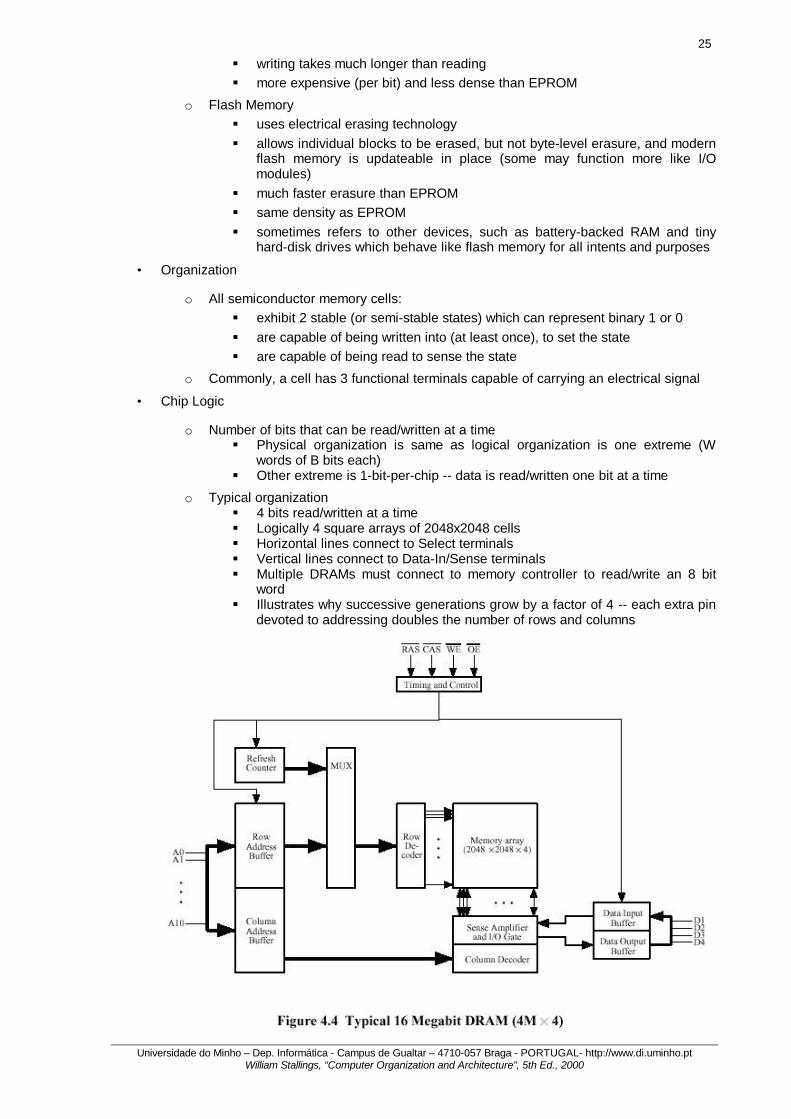
• Chip Logic
o Number of bits that can be read/written at a time § Physical organization is same as logical organization is one extreme (W
words of B bits each) § Other extreme is 1-bit-per-chip -- data is read/written one bit at a time
o Typical organization § 4 bits read/written at a time § Logically 4 square arrays of 2048x2048 cells § Horizontal lines connect to Select terminals § Vertical lines connect to Data-In/Sense terminals § Multiple DRAMs must connect to memory controller to read/write an 8 bit
word § Illustrates why successive generations grow by a factor of 4 -- each extra pin
devoted to addressing doubles the number of rows and columns
26
Universidade do Minho – Dep. Informática - Campus de Gualtar – 4710-057 Braga - PORTUGAL- http://www.di.uminho.pt William Stallings, “Computer Organization and Architecture”, 5th Ed., 2000
• Chip Packaging
o Typical Pin outs § A0-An: Address of word being accessed (may be multiplexed row/column) for
an n bit (n*2 bit) address § D0-Dn: Data in/out for n bits § Vcc: Power supply § Vss: Ground § CE: Chip enable - allows several chips to use same circuits for everything
else, but only have one chip use them § Vpp: Program Voltage - used for writes to (programming) an EPROM § RAS: Row Address Select § CAS: Column Address Select § W or WE: Write enable § OE: Output enable
• Error Correction Principles
o Hard Failure § a permanent defect § causes same result all the time, or randomly fluctuating results
o Soft Error - a random, nondestructive event that alters the contents of one or more memory cells, without damaging the memory. Caused by: § power supply problems § alpha particles
o Detection and Correction
• Hamming codes
o An error-correcting code are characterized by the number of bit errors in a word that it can correct and detect
o The Hamming Code is the simplest error-correcting code. For example, a hamming code for 4 data bits (1110) requires 3 parity bits (100), as shown (to make number of 1’s in a circle even): Note that the parity bits (10) are now incorrect, and their intersection identifies the data bit in error, which can be corrected back to (1) by negation.
• SEC-DED (single-error-correcting, double-error-detecting) codes
o Note that an error of more than a single bit cannot be corrected with the previous method (called a single-error-correcting code).
o Instead, we can add an additional bit to make the total number of 1’s (in both data and parity bits) even. If this bit compares differently, we know that a double error has been detected (although we cannot correct it)
Cache Memory (4.3)
• Principles
o Intended to give memory speed approaching that of fastest memories available but with large size, at close to price of slower memories
o Cache is checked first for all memory references.
o If not found, the entire block in which that reference resides in main memory is stored in a cache slot, called a line
o Each line includes a tag (usually a portion of the main memory address) which identifies which particular block is being stored
o Locality of reference implies that future references will likely come from this block of memory, so that cache line will probably be utilized repeatedly.
27
Universidade do Minho – Dep. Informática - Campus de Gualtar – 4710-057 Braga - PORTUGAL- http://www.di.uminho.pt William Stallings, “Computer Organization and Architecture”, 5th Ed., 2000
o The proportion of memory references, which are found already stored in cache, is called the hit ratio.
• Elements of Cache Design
o Cache Size § small enough that overall average cost/bit is close to that of main memory
alone § large enough so that overall average access time is close to that of cache
alone § large caches tend to be slightly slower than small ones § available chip and board area is a limitation § studies indicate that 1K-512K words is optimum cache size
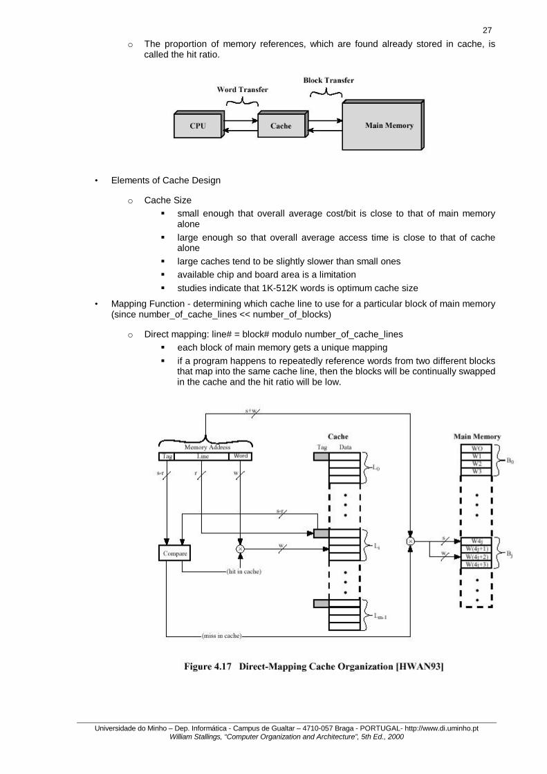
• Mapping Function - determining which cache line to use for a particular block of main memory (since number_of_cache_lines << number_of_blocks)
o Direct mapping: line# = block# modulo number_of_cache_lines § each block of main memory gets a unique mapping § if a program happens to repeatedly reference words from two different blocks
that map into the same cache line, then the blocks will be continually swapped in the cache and the hit ratio will be low.
28
Universidade do Minho – Dep. Informática - Campus de Gualtar – 4710-057 Braga - PORTUGAL- http://www.di.uminho.pt William Stallings, “Computer Organization and Architecture”, 5th Ed., 2000
Note that § all locations in a single block of memory have the same higher order bits (call
them the block number), so the lower order bits can be used to find a particular word in the block.
§ within those higher-order bits, their lower-order bits obey the modulo mapping given above (assuming that the number of cache lines is a power of 2), so they can be used to get the cache line for that block
§ the remaining bits of the block number become a tag, stored with each cache line, and used to distinguish one block from another that could fit into that same cache line.
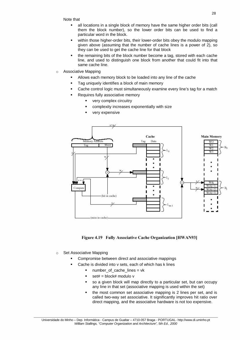
o Associative Mapping § Allows each memory block to be loaded into any line of the cache § Tag uniquely identifies a block of main memory § Cache control logic must simultaneously examine every line’s tag for a match § Requires fully associative memory
§ very complex circuitry § complexity increases exponentially with size § very expensive
o Set Associative Mapping § Compromise between direct and associative mappings § Cache is divided into v sets, each of which has k lines
§ number_of_cache_lines = vk § set# = block# modulo v § so a given block will map directly to a particular set, but can occupy
any line in that set (associative mapping is used within the set) § the most common set associative mapping is 2 lines per set, and is
called two-way set associative. It significantly improves hit ratio over direct mapping, and the associative hardware is not too expensive.
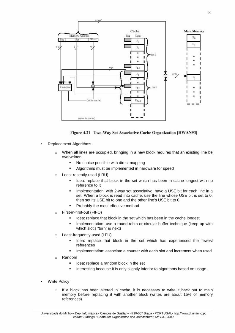
29
Universidade do Minho – Dep. Informática - Campus de Gualtar – 4710-057 Braga - PORTUGAL- http://www.di.uminho.pt William Stallings, “Computer Organization and Architecture”, 5th Ed., 2000
• Replacement Algorithms
o When all lines are occupied, bringing in a new block requires that an existing line be overwritten § No choice possible with direct mapping § Algorithms must be implemented in hardware for speed
o Least-recently-used (LRU) § Idea: replace that block in the set which has been in cache longest with no
reference to it § Implementation: with 2-way set associative, have a USE bit for each line in a
set. When a block is read into cache, use the line whose USE bit is set to 0, then set its USE bit to one and the other line’s USE bit to 0.
§ Probably the most effective method
o First-in-first-out (FIFO) § Idea: replace that block in the set which has been in the cache longest § Implementation: use a round-robin or circular buffer technique (keep up with
which slot’s “turn” is next)
o Least-frequently-used (LFU) § Idea: replace that block in the set which has experienced the fewest
references § Implementation: associate a counter with each slot and increment when used
o Random § Idea: replace a random block in the set § Interesting because it is only slightly inferior to algorithms based on usage.
• Write Policy
o If a block has been altered in cache, it is necessary to write it back out to main memory before replacing it with another block (writes are about 15% of memory references)
30
Universidade do Minho – Dep. Informática - Campus de Gualtar – 4710-057 Braga - PORTUGAL- http://www.di.uminho.pt William Stallings, “Computer Organization and Architecture”, 5th Ed., 2000
o Problems § I/O modules may be able to read/write directly to memory § Multiple CPU’s may be attached to the same bus, each with their own cache
o write through § all write operations are made to main memory as well as to cache, so main
memory is always valid § other CPU’s monitor traffic to main memory to update their caches when
needed § this generates substantial memory traffic and may create a bottleneck
o write back § when an update occurs, an UPDATE bit associated with that slot is set, so
when the block is replaced it is written back first § accesses by I/O modules must occur through the cache § multiple caches still can become invalidated, unless some cache coherency
system is used. Such systems include: § Bus Watching with Write Through - other caches monitor memory
writes by other caches (using write through) and invalidates their own cache line if a match
§ Hardware Transparency - additional hardware links multiple caches so that writes to one cache are made to the others
§ Non-cacheable Memory - only a portion of main memory is shared by more than one processor, and it is non-cacheable
• Block Size
o As the block size increases, more useful data is brought into the cache, increasing hit ratio, BUT
o Larger blocks reduce the number of blocks that fit into a cache, and a small number of blocks results in data being overwritten shortly after it is fetched
o As a block becomes larger, each additional word is farther from the requested word, therefore less likely to be needed in the near future
o A size from 4 to 8 addressable units seems close to optimum
• Number of Caches
o On-chip cache (L1 cache) § on same chip as CPU § requires no bus operation for cache hits § short data paths and same speed as other CPU transactions § reduces overall bus activity and increases not only CPU operations but overall
system performance
o Off-chip cache (L2 cache) may still be desirable § It can be much larger § It can be used with a local bus to buffer the CPU cache-misses from the
system bus
• Unified vs. Split Cache
o Unified cache § a single cache stores both data and instructions § has a higher hit rate that split cache, because it automatically balances load
between data and instructions (if an execution pattern involves more instruction fetches than data fetches, the cache will fill up with more instructions than data)
§ only one cache need be designed and implemented
31
Universidade do Minho – Dep. Informática - Campus de Gualtar – 4710-057 Braga - PORTUGAL- http://www.di.uminho.pt William Stallings, “Computer Organization and Architecture”, 5th Ed., 2000
o In a split cache, one cache is dedicated to instructions, and one cache is dedicated to data § trend is toward split cache because of superscalar CPU’s § better for pipelining, prefetching, and other parallel instruction execution
designs § eliminates cache contention between instruction processor and the execution
unit (which uses data) Pentium Cache Organization (4.4 + … )
• Evolution
o 80386 - No on-chip cache
o 80486 - unified 8Kbyte on-chip cache (16 byte line, 4-way set associative)
o Pentium - two 8Kbyte on-chip caches split between data and instructions (32 byte line, two-way set associative)
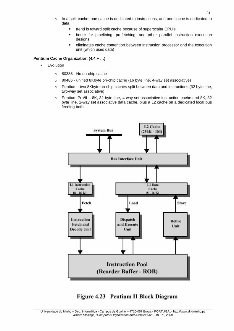
o Pentium Pro/II – 8K, 32 byte line, 4-way set associative instruction cache and 8K, 32 byte line, 2-way set associative data cache, plus a L2 cache on a dedicated local bus feeding both.
32
Universidade do Minho – Dep. Informática - Campus de Gualtar – 4710-057 Braga - PORTUGAL- http://www.di.uminho.pt William Stallings, “Computer Organization and Architecture”, 5th Ed., 2000
• Data Cache Internal Organization
o Basics § Ways
§ 128 sets of two lines each § Logically organized as two 4Kbyte “ways” (each way contains one
line from each set, for 128 lines per way) § Directories
§ Each line has a tag taken from the 20 most significant bits of the memory address of the data stored in the corresponding line
§ Each line has two state bits, one of which is used to support a write-back policy (write-through can be dynamically configured)
§ Logically organized as 2 directories, corresponding to the ways (one directory entry for each line)
§ LRU support § Cache controller uses a least-recently-used replacement policy § A single array of 128 LRU bits supports both ways (one bit for each
set of two lines) § Level-2 cache is supported
§ May be 256 or 512 Kbytes § May use a 32-, 64-, or 128-byte line § Two-way set associative
• Data Cache Consistency
o Supports MESI protocol § Supported by the two state bits mentioned earlier § Each line can be in one of 4 states:
§ Modified - The line in the cache has been modified and is available only in this cache
§ Exclusive - The line in the cache is the same as that in main memory and is not present in any other cache
§ Shared - The line in the cache is the same as that in main memory and may be present in another cache
§ Invalid - The line in the cache dopes not contain valid data § Designed to support multiprocessor organizations, but also useful for
managing consistency between L1 and L2 caches in a single processor organization. § In such an organization, the L2 cache acts as the “memory” that is
cached by the L1 cache. § So when MESI refers to a line being “the same as memory” (or not), it
may be referring to the contents of another cache. PowerPC Cache Organization (… 4.4)
• Evolution
o PowerPC 601 - Unified 32Kbyte on-chip cache (32 byte line, 8-way set associative)
o PowerPC 603 - two 8Kbyte on-chip caches split between data and instructions (32 byte line, two-way set associative)
o PowerPC 604 - two 16Kbyte on-chip caches split between data and instructions (32 byte line, 4-way set associative)
o PowerPC 620 - two 32Kbyte on-chip caches split between data and instructions (64 byte line, 8-way set associative)
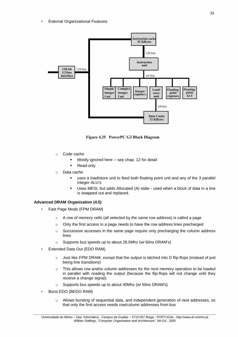
33
Universidade do Minho – Dep. Informática - Campus de Gualtar – 4710-057 Braga - PORTUGAL- http://www.di.uminho.pt William Stallings, “Computer Organization and Architecture”, 5th Ed., 2000
• External Organizational Features
o Code cache § Mostly ignored here -- see chap. 12 for detail § Read-only
o Data cache § uses a load/store unit to feed both floating point unit and any of the 3 parallel
integer ALU’s § Uses MESI, but adds Allocated (A) state - used when a block of data in a line
is swapped out and replaced. Advanced DRAM Organization (4.5)
• Fast Page Mode (FPM DRAM)
o A row of memory cells (all selected by the same row address) is called a page
o Only the first access in a page needs to have the row address lines precharged
o Successive accesses in the same page require only precharging the column address lines
o Supports bus speeds up to about 28.5Mhz (w/ 60ns DRAM’s)
• Extended Data Out (EDO RAM)
o Just like FPM DRAM, except that the output is latched into D flip-flops (instead of just being line transitions)
o This allows row and/or column addresses for the next memory operation to be loaded in parallel with reading the output (because the flip-flops will not change until they receive a change signal)
o Supports bus speeds up to about 40Mhz (w/ 60ns DRAM’s)
• Burst EDO (BEDO RAM)
o Allows bursting of sequential data, and independent generation of next addresses, so that only the first access needs row/column addresses from bus
34
Universidade do Minho – Dep. Informática - Campus de Gualtar – 4710-057 Braga - PORTUGAL- http://www.di.uminho.pt William Stallings, “Computer Organization and Architecture”, 5th Ed., 2000
o Supports bus speeds up to 66Mhz
• Enhanced DRAM
o Developed by Ramtron
o Integrates a small SRAM cache which stores contents of last 512-nibble row read
o Refresh is in parallel to cache reads
o dual ported - reads can be done in parallel with writes
• Cache DRAM
o Developed by Mitsubishi
o Similar to EDRAM, but: § uses a larger cache - 16K vs. 2K § uses a true cache, consisting of 64-bit lines § cache can also be used as a buffer to support the serial access of a block of
data
• Synchronous DRAM
o Developed jointly by several manufacturers
o Standard DRAM is asynchronous § Memory controller watches for read request and address lines § After request is made, bus master must wait while DRAM responds § Bus master watches acknowledgment lines for operation to complete (and
must wait in the meantime)
o Synchronous DRAM moves data in an out in a set number of clock cycles, synchronized with the system clock, just like the processor
o Other speedups § burst mode - after first access, no address setup or row/column line
precharge time is needed § dual-bank internal architecture improves opportunities for on-chip parallelism § mode register allows burst length, burst type, and latency (between receipt of
a read request and beginning of data transfer) to be customized to suit specific system needs
o Current standard works with bus speeds up to 100Mhz (while bursting), or 75Mhz for so-called SDRAM Lite.
• Rambus DRAM
o Developed by Rambus
o Vertical package, all pins on one side, designed to plug into the RDRAM bus (a special high speed bus just for memory)
o After initial 480 ns access time, provides burst speeds of 500 Mbps (compared w/ about 33 Mbps for asynchronous DRAM’s)
• RamLink
o Developed as part of the IEEE working group effort called Scalable Coherent Interface (SCI)
o DRAM chips act as nodes in a ring network
o Data is exchanged in packets § Controller sends a request packet to initiate mem transaction, containing cmd
header, address, checksum, and data to be written (if a write). Extra data in cmd header allows more efficient access.
o Supports a small or large number of DRAM’s
o Does not dictate internal DRAM structure
35
Universidade do Minho – Dep. Informática - Campus de Gualtar – 4710-057 Braga - PORTUGAL- http://www.di.uminho.pt William Stallings, “Computer Organization and Architecture”, 5th Ed., 2000
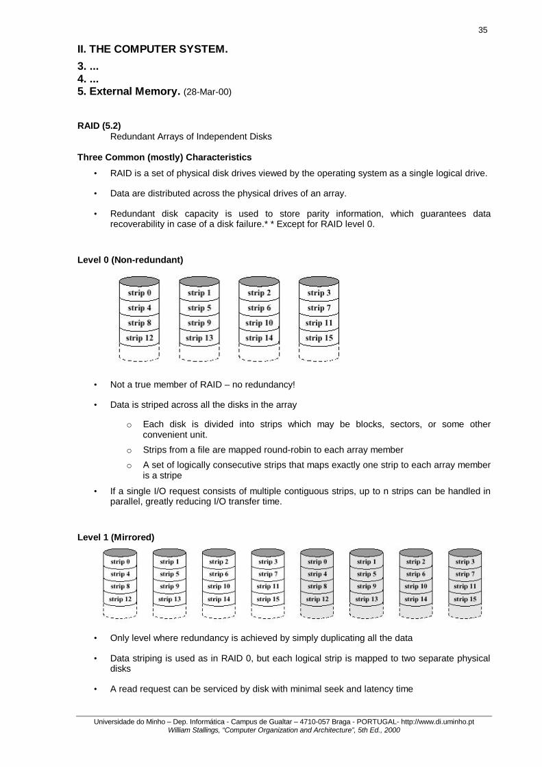
II. THE COMPUTER SYSTEM. 3. ... 4. ... 5. External Memory. (28-Mar-00) RAID (5.2)
Redundant Arrays of Independent Disks Three Common (mostly) Characteristics
• RAID is a set of physical disk drives viewed by the operating system as a single logical drive.
• Data are distributed across the physical drives of an array.
• Redundant disk capacity is used to store parity information, which guarantees data recoverability in case of a disk failure.* * Except for RAID level 0.
Level 0 (Non-redundant)
• Not a true member of RAID – no redundancy!
• Data is striped across all the disks in the array
o Each disk is divided into strips which may be blocks, sectors, or some other convenient unit.
o Strips from a file are mapped round-robin to each array member
o A set of logically consecutive strips that maps exactly one strip to each array member is a stripe
• If a single I/O request consists of multiple contiguous strips, up to n strips can be handled in parallel, greatly reducing I/O transfer time.
Level 1 (Mirrored)
• Only level where redundancy is achieved by simply duplicating all the data
• Data striping is used as in RAID 0, but each logical strip is mapped to two separate physical disks
• A read request can be serviced by disk with minimal seek and latency time
36
Universidade do Minho – Dep. Informática - Campus de Gualtar – 4710-057 Braga - PORTUGAL- http://www.di.uminho.pt William Stallings, “Computer Organization and Architecture”, 5th Ed., 2000
• Write requests require updating 2 disks, but both can be updated in parallel, so no penalty
• When a drive fails, data may be accessed from other drive
• High cost for high performance
o Usually used only for highly critical data.
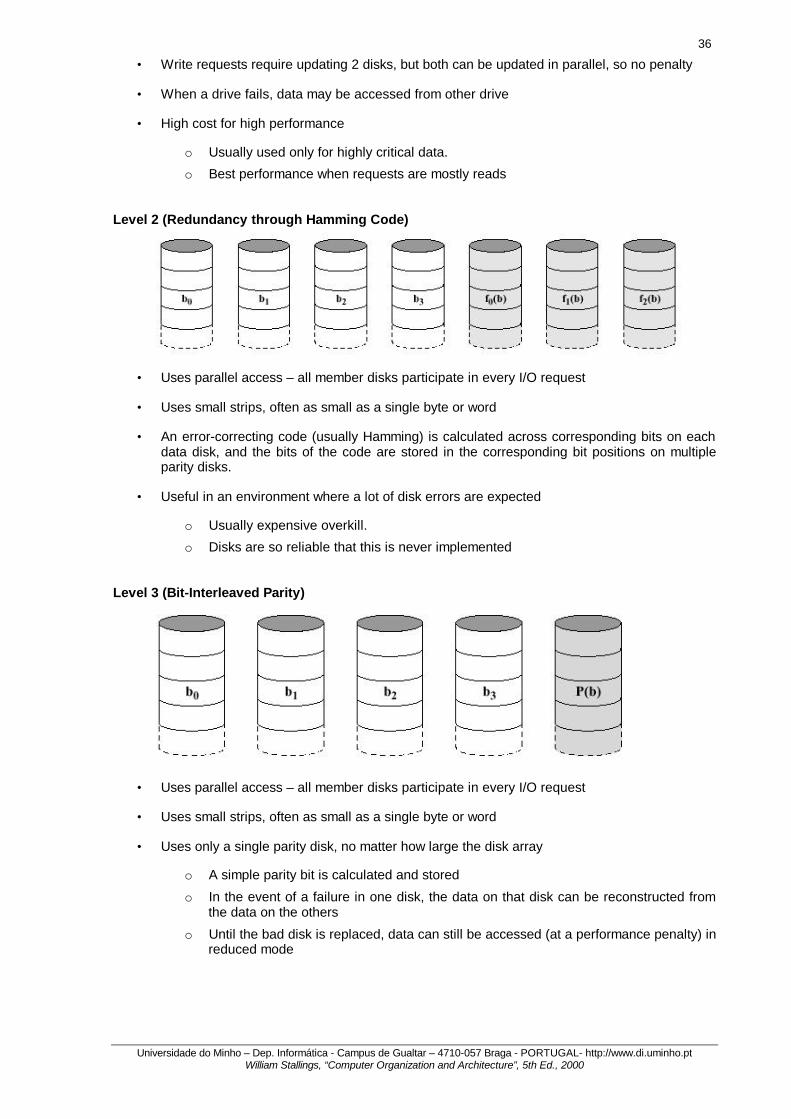
o Best performance when requests are mostly reads Level 2 (Redundancy through Hamming Code)
• Uses parallel access – all member disks participate in every I/O request
• Uses small strips, often as small as a single byte or word
• An error-correcting code (usually Hamming) is calculated across corresponding bits on each data disk, and the bits of the code are stored in the corresponding bit positions on multiple parity disks.
• Useful in an environment where a lot of disk errors are expected
o Usually expensive overkill.
o Disks are so reliable that this is never implemented Level 3 (Bit-Interleaved Parity)
• Uses parallel access – all member disks participate in every I/O request
• Uses small strips, often as small as a single byte or word
• Uses only a single parity disk, no matter how large the disk array
o A simple parity bit is calculated and stored
o In the event of a failure in one disk, the data on that disk can be reconstructed from the data on the others
o Until the bad disk is replaced, data can still be accessed (at a performance penalty) in reduced mode
37
Universidade do Minho – Dep. Informática - Campus de Gualtar – 4710-057 Braga - PORTUGAL- http://www.di.uminho.pt William Stallings, “Computer Organization and Architecture”, 5th Ed., 2000
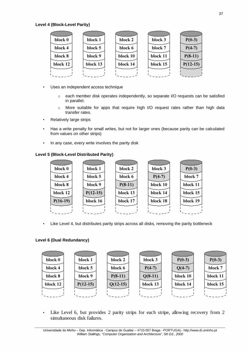
Level 4 (Block-Level Parity)
• Uses an independent access technique
o each member disk operates independently, so separate I/O requests can be satisfied in parallel.
o More suitable for apps that require high I/O request rates rather than high data transfer rates.
• Relatively large strips
• Has a write penalty for small writes, but not for larger ones (because parity can be calculated from values on other strips)
• In any case, every write involves the parity disk
Level 5 (Block-Level Distributed Parity)
• Like Level 4, but distributes parity strips across all disks, removing the parity bottleneck
Level 6 (Dual Redundancy)
• Like Level 6, but provides 2 parity strips for each stripe, allowing recovery from 2 simultaneous disk failures.
38
Universidade do Minho – Dep. Informática - Campus de Gualtar – 4710-057 Braga - PORTUGAL- http://www.di.uminho.pt William Stallings, “Computer Organization and Architecture”, 5th Ed., 2000
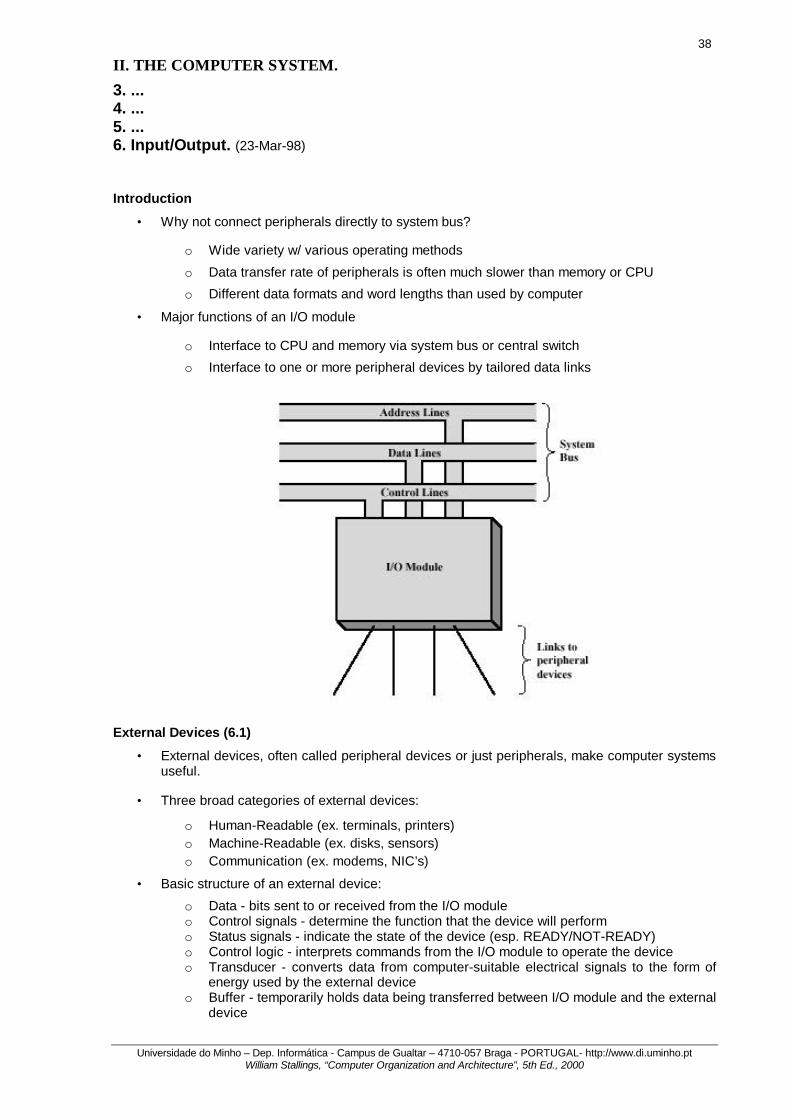
II. THE COMPUTER SYSTEM. 3. ... 4. ... 5. ... 6. Input/Output. (23-Mar-98) Introduction
• Why not connect peripherals directly to system bus?
o Wide variety w/ various operating methods
o Data transfer rate of peripherals is often much slower than memory or CPU
o Different data formats and word lengths than used by computer
• Major functions of an I/O module
o Interface to CPU and memory via system bus or central switch
o Interface to one or more peripheral devices by tailored data links
External Devices (6.1)
• External devices, often called peripheral devices or just peripherals, make computer systems useful.
• Three broad categories of external devices:
o Human-Readable (ex. terminals, printers) o Machine-Readable (ex. disks, sensors) o Communication (ex. modems, NIC’s)
• Basic structure of an external device:
o Data - bits sent to or received from the I/O module o Control signals - determine the function that the device will perform o Status signals - indicate the state of the device (esp. READY/NOT-READY) o Control logic - interprets commands from the I/O module to operate the device o Transducer - converts data from computer-suitable electrical signals to the form of
energy used by the external device o Buffer - temporarily holds data being transferred between I/O module and the external
device
39
Universidade do Minho – Dep. Informática - Campus de Gualtar – 4710-057 Braga - PORTUGAL- http://www.di.uminho.pt William Stallings, “Computer Organization and Architecture”, 5th Ed., 2000
I/O Modules (6.2)
• An I/O Module is the entity within a computer responsible for:
o control of one or more external devices o exchange of data between those devices and main memory and/or CPU registers
• It must have two interfaces:
o internal, to CPU and main memory
o external, to the device(s)
• Major function/requirement categories
o Control and Timing § Coordinates the flow of traffic between internal resources and external
devices § Cooperation with bus arbitration
o CPU Communication § Command Decoding § Data § Status Reporting § Address Recognition.
o Device Communication (see diagram under External Devices) § Commands § Status Information § Data
o Data Buffering § Rate of data transfer to/from CPU is orders of magnitude faster than to/from
external devices § I/O module buffers data so that peripheral can send/receive at its rate, and
CPU can send/receive at its rate
o Error Detection § Must detect and correct or report errors that occur § Types of errors
§ Mechanical/electrical malfunctions § Data errors during transmission
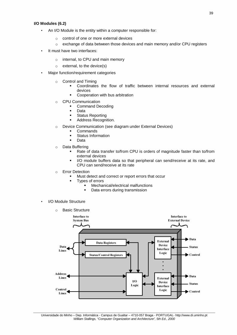
• I/O Module Structure
o Basic Structure
40
Universidade do Minho – Dep. Informática - Campus de Gualtar – 4710-057 Braga - PORTUGAL- http://www.di.uminho.pt William Stallings, “Computer Organization and Architecture”, 5th Ed., 2000
o An I/O module functions to allow the CPU to view a wide range of devices in a simple-minded way.
o A spectrum of capabilities may be provided § I/O channel or I/O processor - takes on most of the detailed processing
burden, presenting a high-level interface to CPU § I/O controller or device controller - quite primitive and requires detailed control § I/O module - generic, used when no confusion results
Programmed I/O (6.3)
• With programmed I/O, data is exchanged under complete control of the CPU
o CPU encounters an I/O instruction
o CPU issues a command to appropriate I/O module
o I/O module performs requested action and sets I/O status register bits
o CPU must wait, and periodically check I/O module status until it finds that the operation is complete
• To execute an I/O instruction, the CPU issues:
o an address, specifying I/O module and external device
o a command, 4 types: § control - activate a peripheral and tell it what to do § test - querying the state of the module or one of its external devices § read - obtain an item of data from the peripheral and place it in an internal
buffer (data register from preceding illustration) § write - take an item of data from the data bus and transmit it to the peripheral
• With programmed I/O, there is a close correspondence between the I/O instructions used by the CPU and the I/O commands issued to an I/O module
• Each I/O module must interpret the address lines to determine if a command is for itself.
• Two modes of addressing are possible:
o Memory-mapped I/O § there is a single address space for memory locations and I/O devices. § allows the same read/write lines to be used for both memory and I/O
transactions
o Isolated I/O § full address space may be used for either memory locations or I/O devices. § requires an additional control line to distinguish memory transactions from I/O
transactions § programmer loses repertoire of memory access commands, but gains
memory address space Interrupt-Driven I/O (6.4)
• Problem with programmed I/O is CPU has to wait for I/O module to be ready for either reception or transmission of data, taking time to query status at regular intervals.
• Interrupt-driven I/O is an alternative
o It allows the CPU to go back to doing useful work after issuing an I/O command.
o When the command is completed, the I/O module will signal the CPU that it is ready with an interrupt.
• Simple Interrupt Processing Diagram
41
Universidade do Minho – Dep. Informática - Campus de Gualtar – 4710-057 Braga - PORTUGAL- http://www.di.uminho.pt William Stallings, “Computer Organization and Architecture”, 5th Ed., 2000
• Design issues
o How does the CPU determine which device issued the interrupt? § Multiple Interrupt Lines
§ most straightforward solution § impractical to dedicate many lines
§ multiple I/O modules are likely attached to each line § one of other 3 techniques must be used on each line
§ Software Poll § interrupt service routine polls each device to see which caused the
interrupt § using a separate command line on the system bus (TESTI/O)
? raise TESTI/O ? place I/O module address on address lines ? check for affirmative response
§ each I/O module contains an addressable status register, which CPU reads
§ time consuming § Daisy Chain (hardware poll, vectored)
§ interrupt occurs on interrupt request line which is shared by all I/O modules
§ CPU senses interrupt § CPU sends interrupt acknowledge, which is daisy-chained through all
I/O modules § When it gets to requesting module, it places its vector (either an I/O
address, or an ID which the CPU uses as a pointer to the appropriate device-service routine) on the data lines
§ No general interrupt-service routine needed (still need specific ones) § Bus Arbitration (vectored)
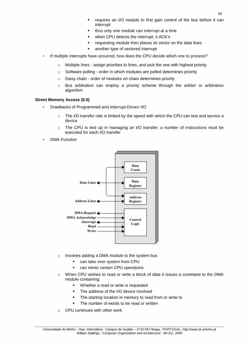
42
Universidade do Minho – Dep. Informática - Campus de Gualtar – 4710-057 Braga - PORTUGAL- http://www.di.uminho.pt William Stallings, “Computer Organization and Architecture”, 5th Ed., 2000
§ requires an I/O module to first gain control of the bus before it can interrupt
§ thus only one module can interrupt at a time § when CPU detects the interrupt, it ACK’s § requesting module then places its vector on the data lines § another type of vectored interrupt
• If multiple interrupts have occurred, how does the CPU decide which one to process?
o Multiple lines - assign priorities to lines, and pick the one with highest priority
o Software polling - order in which modules are polled determines priority
o Daisy chain - order of modules on chain determines priority
o Bus arbitration can employ a priority scheme through the arbiter or arbitration algorithm
Direct Memory Access (6.5)
• Drawbacks of Programmed and Interrupt-Driven I/O
o The I/O transfer rate is limited by the speed with which the CPU can test and service a device
o The CPU is tied up in managing an I/O transfer; a number of instructions must be executed for each I/O transfer
• DMA Function
o Involves adding a DMA module to the system bus § can take over system from CPU § can mimic certain CPU operations
o When CPU wishes to read or write a block of data it issues a command to the DMA module containing: § Whether a read or write is requested § The address of the I/O device involved § The starting location in memory to read from or write to § The number of words to be read or written
o CPU continues with other work
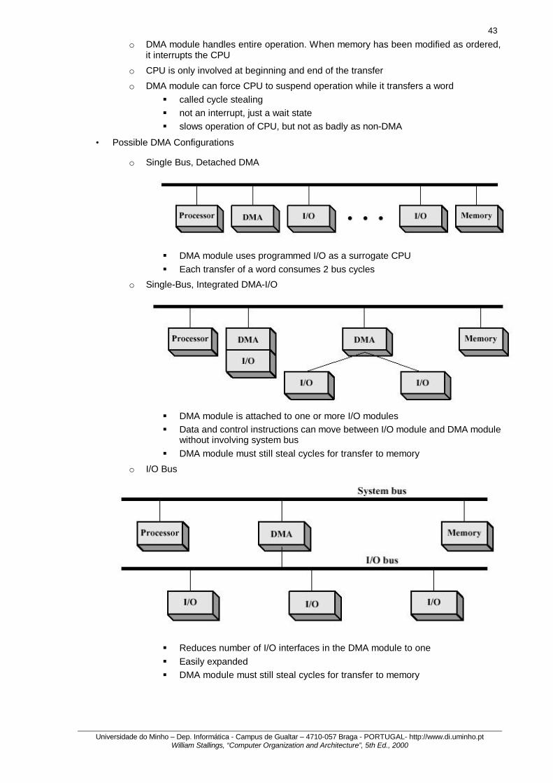
43
Universidade do Minho – Dep. Informática - Campus de Gualtar – 4710-057 Braga - PORTUGAL- http://www.di.uminho.pt William Stallings, “Computer Organization and Architecture”, 5th Ed., 2000
o DMA module handles entire operation. When memory has been modified as ordered, it interrupts the CPU
o CPU is only involved at beginning and end of the transfer
o DMA module can force CPU to suspend operation while it transfers a word § called cycle stealing § not an interrupt, just a wait state § slows operation of CPU, but not as badly as non-DMA
• Possible DMA Configurations
o Single Bus, Detached DMA
§ DMA module uses programmed I/O as a surrogate CPU § Each transfer of a word consumes 2 bus cycles
o Single-Bus, Integrated DMA-I/O
§ DMA module is attached to one or more I/O modules § Data and control instructions can move between I/O module and DMA module
without involving system bus § DMA module must still steal cycles for transfer to memory
o I/O Bus
§ Reduces number of I/O interfaces in the DMA module to one § Easily expanded § DMA module must still steal cycles for transfer to memory
44
Universidade do Minho – Dep. Informática - Campus de Gualtar – 4710-057 Braga - PORTUGAL- http://www.di.uminho.pt William Stallings, “Computer Organization and Architecture”, 5th Ed., 2000
I/O Channels and Processors (6.6)
• Past DMA, we see two evolutionary developments to the I/O module
o The I/O Channel enhances the I/O module to become a processor in its own right § CPU directs I/O module to execute a sequence of special I/O instructions in
memory § I/O channel fetches and executes these instructions without CPU intervention § The CPU is only interrupted when the entire sequence is completed
o The I/O Processor has a local memory of its own, and is a computer in its own right, allowing a large set of devices to be controlled with minimal CPU involvement
• Two common types of I/O channels
o A selector channel § controls multiple high-speed devices § is dedicated to transfer of data with one device at a time § each device is handled by a controller that is very similar to an I/O module § the I/O channel serves in place of the CPU in controlling these I/O controllers
o A multiplexor channel § Handles I/O with multiple controllers at once § Low speed devices use a byte multiplexor § High speed devices use a block multiplexor
The External Interface (6.7)
• Types of interfaces
o Parallel interface - multiple lines connect the I/O module and the peripheral, and multiple bits are transferred simultaneously
o Serial interface - only one line is used to transmit data, one bit at a time
• Typical dialog between I/O module and peripheral (for a write operation)
o The IO module sends a control signal requesting permission to send data
o The peripheral ACK’s the request
o The I/O module transfers the data
o The peripheral ACK’s receiving the data
• Buffer in I/O module compensates for speed differences
• Point-to-Point and Multipoint Configurations
o Point-to-point interface § provides a dedicated line between the I/O module and the external device § examples are keyboard, printer, modem
o Multipoint interface § in effect are external buses § examples are SCSI, USB, IEEE 1394 (FireWire), and even IDE
• SCSI (Small Computer System Interface)
o Standards § SCSI-1 (early ‘80’s)
§ 8 data lines § data rate of 5Mb/s § up to 7 devices daisy-chained to interface
45
Universidade do Minho – Dep. Informática - Campus de Gualtar – 4710-057 Braga - PORTUGAL- http://www.di.uminho.pt William Stallings, “Computer Organization and Architecture”, 5th Ed., 2000
§ SCSI-2 (1991) § usually what is meant today by “SCSI” § 16 or 32 data lines § data rate of 20Mb/s or 40Mb/s (dep. on data lines) § up to 16 devices daisy-chained to interface § includes commands for the following device types:
§ direct-access devices § sequential-access devices § printers § processors § write-once devices § CD-ROM’s § scanners § optical memory devices § medium-changer devices § communication devices
§ SCSI-3 (still in development) § doubles speed of SCSI-2 § includes “serial SCSI”, which is basically FireWire
o Basically defines a high-speed external bus § has its own arbitration § communication can take place between devices (such as disk to tape) without
involving the CPU or other internal buses at all § reselection - if a command is issued that takes some time to complete, the
target can release the bus and reconnect to the initiator later
• P1394 Serial Bus (FireWire)
o Basic features § very high-speed - up to 400Mbps § serial transmission
§ requires less wires § allows simple connector § less potential for damage § requires less shielding w/ no synchronization problems § cheaper
§ physically small - suitable for handheld computers and other small consumer electronics
o Details § Uses a daisy chain configuration
§ up to 63 devices off a single port § up to 1022 P1394 buses can be interconnected using bridges
§ Supports hot plugging - peripherals can be connected and disconnected without power down or reconfiguration
§ Supports automatic configuration § no manual configuration of device ID’s required § relative positioning of devices unimportant
§ Strict daisy-chain not required - trees possible § Basically sets up a bridged bus-type network as the I/O bus
§ data and control information (such as for arbitration) is transferred in packets
§ can function asynchronously § using variable amounts of data and larger packet headers w/
ACK needed § for devices with intermittent need for the bus § can use fair or urgent arbitration
§ can function isochronously § using fixed-size packets transmitted at regular intervals § for devices that regularly transmit or consume data, such as
digital sound or video
46
Universidade do Minho – Dep. Informática - Campus de Gualtar – 4710-057 Braga - PORTUGAL- http://www.di.uminho.pt William Stallings, “Computer Organization and Architecture”, 5th Ed., 2000
II. THE COMPUTER SYSTEM. 3. ... 4. ... 5. ... 6. ... 7. Operating System Support. (30-Mar-98)
Introduction (7.1)
• From an architectural viewpoint, the most important function of an operating system is resource management
o It controls the movement and storage of data
o It allows access to peripheral devices
o It controls which sets of instructions are allowed to process data at a particular time
• But it is an unusual control mechanism, in that:
o It functions in the same way as ordinary computer software -- it is a program executed by the CPU
o It frequently relinquishes control and must depend on the CPU to allow it to regain control
Scheduling (7.2)
• The central task of modern operating systems is multiprogramming - allowing multiple jobs or user programs to be executed concurrently.
• A better term than job (which is rooted in the old batch systems) is process. Several definitions:
o A program in execution
o The “animated spirit” of a program
o That entity to which a processor is assigned
High-Level Scheduling
• High-level scheduling
o Determines which programs are admitted to the system for processing
o Executes relatively infrequently
o Controls the degree of multiprogramming (number of processes in memory)
o Batch systems can make system optimizing decisions on which jobs to add, priorities to assign, etc.
o Once admitted, a job or program becomes a process and is added to a queue for the short-term scheduler
Short-Term Scheduling
• The short-term scheduler, or dispatcher
o determines which process (of those permitted by the high-level scheduler) gets to execute next
o executes frequently
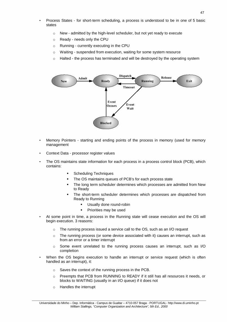
47
Universidade do Minho – Dep. Informática - Campus de Gualtar – 4710-057 Braga - PORTUGAL- http://www.di.uminho.pt William Stallings, “Computer Organization and Architecture”, 5th Ed., 2000
• Process States - for short-term scheduling, a process is understood to be in one of 5 basic states
o New - admitted by the high-level scheduler, but not yet ready to execute
o Ready - needs only the CPU
o Running - currently executing in the CPU
o Waiting - suspended from execution, waiting for some system resource
o Halted - the process has terminated and will be destroyed by the operating system
• Memory Pointers - starting and ending points of the process in memory (used for memory
management
• Context Data - processor register values
• The OS maintains state information for each process in a process control block (PCB), which contains:
§ Scheduling Techniques § The OS maintains queues of PCB’s for each process state § The long term scheduler determines which processes are admitted from New
to Ready § The short-term scheduler determines which processes are dispatched from
Ready to Running § Usually done round-robin § Priorities may be used
• At some point in time, a process in the Running state will cease execution and the OS will begin execution. 3 reasons:
o The running process issued a service call to the OS, such as an I/O request
o The running process (or some device associated with it) causes an interrupt, such as from an error or a timer interrupt
o Some event unrelated to the running process causes an interrupt, such as I/O completion
• When the OS begins execution to handle an interrupt or service request (which is often handled as an interrupt), it:
o Saves the context of the running process in the PCB.
o Preempts that PCB from RUNNING to READY if it still has all resources it needs, or blocks to WAITING (usually in an I/O queue) if it does not
o Handles the interrupt
48
Universidade do Minho – Dep. Informática - Campus de Gualtar – 4710-057 Braga - PORTUGAL- http://www.di.uminho.pt William Stallings, “Computer Organization and Architecture”, 5th Ed., 2000
o Executes the short-term scheduler to pick the next process to dispatch from RUNNING to READY
• Organizational support
o The mode bit in the CPU
o Privileged instruction support in the CPU
o The CPU timer device (a module on the bus) Memory Management (7.3)
• Swapping
o Used when all processes currently in the system become blocked waiting for I/O
o Some waiting processes are swapped out to an intermediate queue in disk storage
o Other processes (which have all the resources they need) are admitted from the long-term queue or swapped in from the intermediate queue to keep the processor busy
• Partitioning
o Memory is partitioned among running processes § the OS kernel (or nucleus) occupies a fixed portion of main memory § remaining memory is partitioned among the other processes
§ fixed-size partitions - different sized partitions are pre-set, and processes are loaded into the smallest that will work. Low processing overhead, but wasteful.
§ variable-size partitions - a process is allocated exactly as much memory as it requires. Fragmentation can still occur to waste memory, however.
§ Requires that program addresses be logical addresses - relative to beginning of program.
o Organizational support in the CPU for partitioning § base address register § limit register
• Paging
o Extends partition idea by dividing up both memory and processes into equal size pieces § pieces of memory are called frames § pieces of a process are called pages
o Each process has a list of frames that it is using, called a page table, stored in the PCB
o The OS maintains a list of free frames that it can assign to new processes
o Only waste is a end of a process’s last page
o Logical addresses become (frame #, rel. addr)
o Organizational support for paging § page table address register in the CPU § cache support for page table lookups
• Virtual Memory
o Refines paging by demand paging - each page of a process is brought in only when needed, that is, on demand.
o Obeys the principle of locality, similar to caching
o If a page is needed which is not in memory, a page fault is triggered, which requires an I/O operation
49
Universidade do Minho – Dep. Informática - Campus de Gualtar – 4710-057 Braga - PORTUGAL- http://www.di.uminho.pt William Stallings, “Computer Organization and Architecture”, 5th Ed., 2000
o Pages currently in memory may have to be replaced. In some situations this can lead to thrashing, where the processor spends too much time swapping the same pages in and out.
o Advantages § Less pages per process, more processes at a time § Unused pages are not swapped in and out anyway § Programs can be longer than all of main memory
§ Main memory, where processes execute is referred to as real memory
§ The memory perceived by the programmer or user is called virtual memory
o Page Table Structure § Basic mechanism for reading a word from memory involves using a page
table to translate § a virtual address - page number and offset
into § a physical address - frame number and offset
o Page tables may be very large § they cannot be stored in registers § they are often stored in virtual memory (so are subject to paging!) § sometimes a page directory is used to organize many pages of page tables.
Pentium uses such a two-level structure § sometimes an inverted page table structure is used to map a virtual address
to a real address using a hash on the page number of the virtual address. AS/400 and PowerPC use this idea.
o Organizational support § Translation Lookaside Buffer (TLB)
§ Avoids problem that every virtual memory reference can cause 2 physical memory accesses § one to fetch appropriate page table entry § one to fetch desired data
§ TLB is a special cache, just for page table entries § Result of address resolution then uses regular cache for fetch
• Segmentation
o Segmentation allows programmer to view memory as multiple address spaces, or segments § Unlike virtual memory, segmentation is not transparent to the programmer § Advantages
§ Simplifies handling of growing data structures - OS will expand or shrink segment as needed
§ Simplifies separate compilation § Lends itself to sharing among processes § Lends itself to protection - programmer or sysadmin can assign
access privileges to a segment
50
Universidade do Minho – Dep. Informática - Campus de Gualtar – 4710-057 Braga - PORTUGAL- http://www.di.uminho.pt William Stallings, “Computer Organization and Architecture”, 5th Ed., 2000
III. THE CENTRAL PROCESSING UNIT. 8. Computer Arithmetic. (19-Apr-99) Integer Representation (8.2)
• Sign-Magnitude Representation
o Leftmost bit is sign bit: 0 for positive, 1 for negative
o Remaining bits are magnitude
o Drawbacks § Addition and subtraction must consider both the signs and relative
magnitudes -- more complex § Testing for zero must consider two possible zero representations
• Two’s Complement Representation
o Leftmost bit still indicates sign
o Positive numbers exactly same as sign-magnitude
o Zero is only all zeroes (positive)
o Negative numbers found by taking 2’s complement § Take complement of positive version § Add 1
Integer Arithmetic (8.3)
• 2’s complement examples (with 8 bit numbers)
o Getting -55 § Start with +55: 0110111 § Complement that: 1001000 § Add 1: +0000001 § Total is -55: 1001001
o Negating -55 § Complement -55: 0110110 § Add 1: +0000001 § Total is 55 (see top) 0110111
o Adding -55 + 58 § Start with -55: 1001001 § Add 58: +0111010 § Result is 3: 0000011 § Overflow into and out-of sign bit is ignored
• Overflow Rule - if two numbers are added, and they are both positive or both negative, then overflow occurs if and only if the result has the opposite sign
• Converting between different bit lengths
o Move sign bit to new leftmost position
o Fill in with copies of the sign bit
o Examples (8 bit -> 16 bit) § +18: 00010010 -> 0000000000010010 § -18: 11101110 -> 1111111111101110
51
Universidade do Minho – Dep. Informática - Campus de Gualtar – 4710-057 Braga - PORTUGAL- http://www.di.uminho.pt William Stallings, “Computer Organization and Architecture”, 5th Ed., 2000
• Multiplication
o Repeated Addition
o Unsigned Integers § Generating partial products, shifting, and adding § Just like longhand multiplication
• Two’s Complement Multiplication
o Straightforward multiplication will not work if either the multiplier or multiplicand are negative § multiplicand would have to be padded with sign bit into a 2n-bit partial
product, so that the signs would line up § in a negative multiplier, the 1’s and 0’s would no longer correspond to add-
shift’s and shift-only’s
o Simple solution § Convert both multiplier and multiplicand to positive numbers § Perform multiplication § Take 2’s complement of result if and only if the signs of original numbers were
different § Other methods do not require this final transformation step
• Booth’s Algorithm
• Why does Booth’s Algorithm work?
o Consider multiplying some multiplicand M by 30: M * (00011110) which would take 4 shift-adds of M (one for each 1)
o That is the same as multiplying M by (32 - 2): M * (00100000 - 00000010) = M * (00100000) - M * (00000010) which would take: § 1 shift-only on no transition (imagine last bit was 0) § 1 shift-subtract on the transition from 0 to 1 § 3 shift-only’s on no transition § 1 shift-add on the transition from 1 to 0 § 2 shift-only’s on no transition
o We can extend this method to any number of blocks of 1’s, including blocks of unit length.
o Consider the smallest number of bits that can hold the 2’s complement representation of -6: So we can clearly see that a shift-subtract at the leftmost 1-0 transition will cause 8 to be subtracted from the accumulated total, which is exactly what needs to happen!
o This will expand to an 8-bit representation: The neat part is that this same (and only) 1-0 transition will also cause -8 to be subtracted from the 8-bit version!
• Division
o Unsigned integers 00001101 Quotient Divisor 1011 10010011 Dividend 1011 001110 1011 001111 1011 100 Remainder
Floating-Point Representation (8.4)
• Principles
o Using scientific notation, we can store a floating point number in 3 parts ±S * B±E : § Sign § Significand (or Mantissa) § Exponent § (The Base stays the same, so need not be stored)
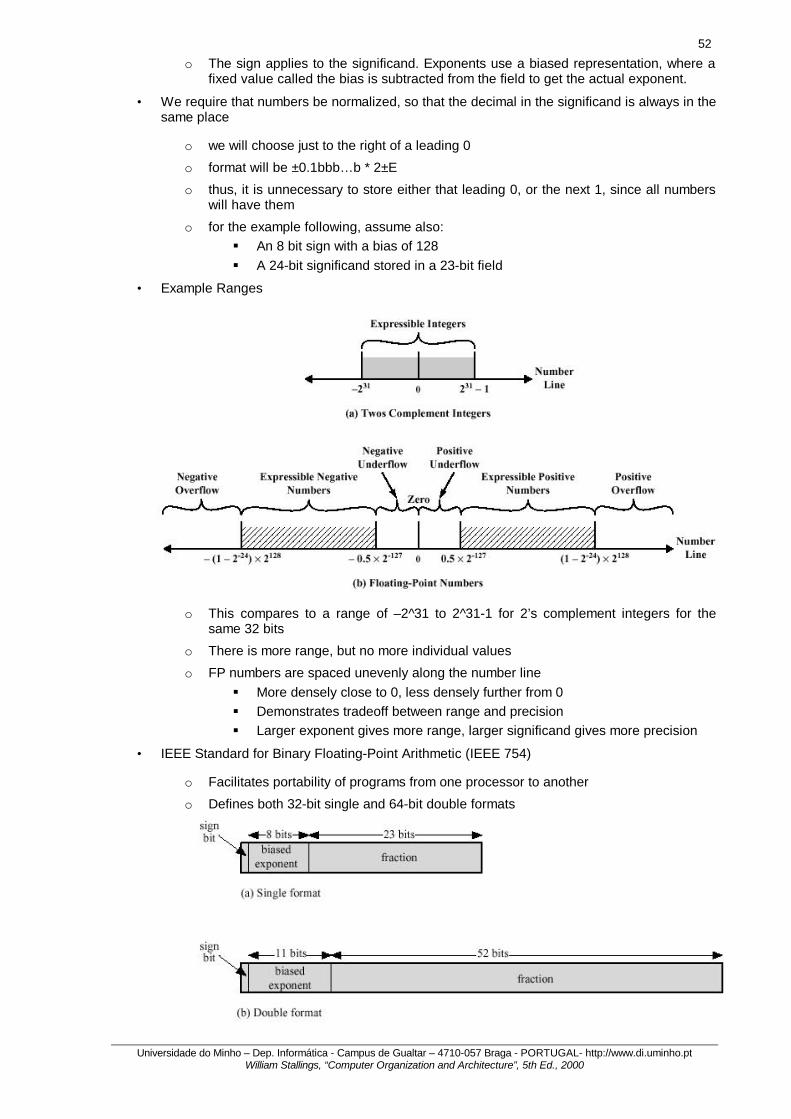
52
Universidade do Minho – Dep. Informática - Campus de Gualtar – 4710-057 Braga - PORTUGAL- http://www.di.uminho.pt William Stallings, “Computer Organization and Architecture”, 5th Ed., 2000
o The sign applies to the significand. Exponents use a biased representation, where a fixed value called the bias is subtracted from the field to get the actual exponent.
• We require that numbers be normalized, so that the decimal in the significand is always in the same place
o we will choose just to the right of a leading 0
o format will be ±0.1bbb… b * 2±E
o thus, it is unnecessary to store either that leading 0, or the next 1, since all numbers will have them
o for the example following, assume also: § An 8 bit sign with a bias of 128 § A 24-bit significand stored in a 23-bit field
• Example Ranges
o This compares to a range of –2^31 to 2^31-1 for 2’s complement integers for the same 32 bits
o There is more range, but no more individual values
o FP numbers are spaced unevenly along the number line § More densely close to 0, less densely further from 0 § Demonstrates tradeoff between range and precision § Larger exponent gives more range, larger significand gives more precision
• IEEE Standard for Binary Floating-Point Arithmetic (IEEE 754)
o Facilitates portability of programs from one processor to another
o Defines both 32-bit single and 64-bit double formats
53
Universidade do Minho – Dep. Informática - Campus de Gualtar – 4710-057 Braga - PORTUGAL- http://www.di.uminho.pt William Stallings, “Computer Organization and Architecture”, 5th Ed., 2000
o Defines some parameters for extending those formats for more range or more precision
• Classes of numbers represented:
o Positive or Negative Zero - an exponent of 0, together with a fraction of zero (sign bit determines sign).
o Positive or Negative Infinity - an exponent of all 1’s, together with a fraction of zero (sign bit determines sign).
o Denormalized Numbers - an exponent of all 1’s except the least significant (which is -0). The fraction is the portion of the significand to the right of the decimal (0 is assumed to the left). Note that the fraction does NOT have an implied leftmost one.
o NaN (Not a Number) - an exponent of all ones, together with a non-zero fraction. Used to signal various exception conditions.
o Normalized, Non-Zero Floating Point Numbers - everything else.
• Potential problems:
o Exponent Overflow - the number is too large to be represented, may be reported as +infinity or -infinity .
o Exponent Underflow - the number is too small to be represented, may be reported as 0.
o Significand Underflow - during alignment of significands, digits may flow off the right end, requiring some form of rounding.
o Significand Overflow - adding two significands with the same sign may result in a carry out of the most significant bit, fixed by realignment.
Floating Point Arithmetic (8.5)
• Addition and Subtraction
o More complex than multiplication and division
o 4 basic phases § Check for zeros § Align the significands § Add or subtract the significands § Normalize the result
o The two operands must be transferred to registers in the ALU § implicit significand bits must be made explicit § exponents and significands usually stored in separate registers
o If subtraction, change sign of subtrahend
o If either operand is 0, report other as result
o Manipulate the numbers so that the two exponents are equal § Ex. 123 x 10^0 + 456 x 10^-2 = 123 x 10^0 + 4.56 x 10^0 = 127.56 x 10^0 § Done by shifting smaller number to the right
§ Simultaneously incrementing the exponent § Stops when exponents are equal § Digits lost are of relatively small importance § If significand becomes 0, report other as result
o The numbers are added together § Signs are taken into account, so zero may result § If significand overflows, the significand of the result is shifted right, and the
exponent is incremented § If exponent then overflows, it is reported and operation halted
54
Universidade do Minho – Dep. Informática - Campus de Gualtar – 4710-057 Braga - PORTUGAL- http://www.di.uminho.pt William Stallings, “Computer Organization and Architecture”, 5th Ed., 2000
o Normalize the result § significand digits are shifted left until the most significant digit is non-zero § exponent is decremented for each shift § If exponent underflows, report it and halt
o Round result and store in proper format
• Multiplication
o The two operands must be transferred to registers in the ALU
o If either operand is 0, report 0 as result
o Add the exponents § If a biased exponent is being used, subtract the extra bias from the sum § Check for exponent overflow or underflow. Report it and halt if it occurs.
o Multiply the significands § Same as for integers, but sign-magnitude representation § Product will be double length of multiplier and multiplicand, but extra bits will
be lost during rounding
o Result is normalized and rounded § Same as for addition and subtraction § Thus, exponent underflow could result
• Division
o The two operands must be transferred to registers in the ALU
o Check for 0 § If divisor is 0, report error and either set result to infinity or halt operation § if dividend is 0, report 0 as result
o Subtract divisor exponent from dividend exponent § If a biased exponent is being used, add the bias back in. § Check for exponent overflow or underflow. Report it and halt if it occurs.
o Divide the significands § Same as for integers, but sign-magnitude representation
o Result is normalized and rounded § Same as for addition and subtraction § Thus, exponent underflow could result
• Precision Considerations
o Guard Bits § Extra bits that pad out the right end of the significand with 0’s § Used to prevent loss of precision when adding numbers which are very close
in value § Example without guard bits: 1.0000000 * 2^1 + -1.1111111 * 2^0 = 1.0000000 * 2^1 + -0.1111111 * 2^1 = 0.0000001 * 2^1 Normalized to: 1.0000000 * 2^-7 § Example with guard bits: 1.00000000 * 2^1+ -1.11111110 * 2^0 = 1.00000000 * 2^1 + -0.11111111 * 2^1 = 0.00000001 * 2^1 Normalized to: 1.00000000 * 2^-8
55
Universidade do Minho – Dep. Informática - Campus de Gualtar – 4710-057 Braga - PORTUGAL- http://www.di.uminho.pt William Stallings, “Computer Organization and Architecture”, 5th Ed., 2000
§ Notice the order of magnitude difference in results! Difference is worse with base-16 architectures.
o Rounding § 4 alternative approaches with IEEE standard § Round to Nearest § Result is rounded to nearest representable number § Default rounding mode § The representable value nearest to the infinitely precise result shall be
delivered * if excess bits are less than half of last representable bit, round down * if excess bits are half or more of last representable bit, round up * if they are equally close, use the one with LSB 0
§ Round Toward + infinity and -infinity § Result is rounded up toward positive infinity or Result is rounded down
toward negative infinity § Useful in implementing interval arithmetic * every calculation in a
sequence is done twice -- once rounding up, and once rounding down, producing upper and lower bounds on the result. * if resulting range is narrow enough, then answer is sufficiently accurate * useful because hardware limitations cause rounding
§ Round Toward 0 § Result is rounded toward 0 § Just simple truncation § Result is always less than or equal to the more precise original value,
introducing a consistent downward bias
• IEEE Standard for Floating Point Arithmetic
o Infinity § Most operations involving infinity yield infinity § Signs obey usual laws § -infinity -infinity yields -infinity and +infinity +infinity yields +infinity
o Quiet and Signaling NaN’s § A signaling NaN causes an exception (which may be handled by the program,
or may cause an error)
• A quiet NaN propagates through operations in an expression without signaling an exception. They are produced by:
o Any operation on a signaling NaN
o Magnitude subtraction of infinities (where you might expect a zero result)
o 0 x infinity
o (0 / 0) or (infinity / infinity ). Note that x / 0 is always an exception.
o (x MOD 0) or (infinity MOD y)
o square-root of x, where x < 0
• Denormalized Numbers
o Used in case of exponent underflow
o When the exponent of the result is too small ( a negative exponent with too large a magnitude) the result is denormalized § right-shifting the fraction § incrementing the exponent for each shift, until it is all ones with a final 0
o Referred to as gradual underflow, use of denormalized numbers: § fills the gap between the smallest representable non-zero number and 0 § reduces the impact of exponent underflow to a level comparable to round off
among the normalized numbers
56
Universidade do Minho – Dep. Informática - Campus de Gualtar – 4710-057 Braga - PORTUGAL- http://www.di.uminho.pt William Stallings, “Computer Organization and Architecture”, 5th Ed., 2000
III. THE CENTRAL PROCESSING UNIT.
8. ... 9. ... 10. ... 11. CPU Structure and Function. (29-Apr-98)
Processor Organization (11.1)
• Things a CPU must do:
o Fetch Instructions
o Interpret Instructions
o Fetch Data
o Process Data
o Write Data
• A small amount of internal memory, called the registers, is needed by the CPU to fulfill these requirements
Register Organization (11.2)
• Registers are at top of the memory hierarchy. They serve two functions:
o User-Visible Registers - enable the machine- or assembly-language programmer to minimize main-memory references by optimizing use of registers
o Control and Status Registers - used by the control unit to control the operation of the CPU and by privileged, OS programs to control the execution of programs
• User-Visible Registers
o Categories of Use § General Purpose § Data § Address § Segment pointers - hold base address of the segment in use § Index registers - used for indexed addressing and may be auto indexed § Stack Pointer - a dedicated register that points to top of a stack. Push,
pop, and other stack instructions need not contain an explicit stack operand.
§ Condition Codes
o Design Issues § Completely general-purpose registers, or specialized use?
§ Specialized registers save bits in instructions because their use can be implicit
§ General-purpose registers are more flexible § Trend is toward use of specialized registers
§ Number of registers provided? § More registers require more operand specifier bits in instructions § 8 to 32 registers appears optimum (RISC systems use hundreds, but
are a completely different approach) § Register Length?
§ Address registers must be long enough to hold the largest address § Data registers should be able to hold values of most data types § Some machines allow two contiguous registers for double-length
values
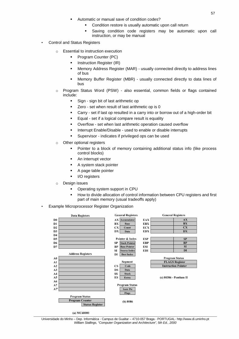
57
Universidade do Minho – Dep. Informática - Campus de Gualtar – 4710-057 Braga - PORTUGAL- http://www.di.uminho.pt William Stallings, “Computer Organization and Architecture”, 5th Ed., 2000
§ Automatic or manual save of condition codes? § Condition restore is usually automatic upon call return § Saving condition code registers may be automatic upon call
instruction, or may be manual
• Control and Status Registers
o Essential to instruction execution § Program Counter (PC) § Instruction Register (IR) § Memory Address Register (MAR) - usually connected directly to address lines
of bus § Memory Buffer Register (MBR) - usually connected directly to data lines of
bus
o Program Status Word (PSW) - also essential, common fields or flags contained include: § Sign - sign bit of last arithmetic op § Zero - set when result of last arithmetic op is 0 § Carry - set if last op resulted in a carry into or borrow out of a high-order bit § Equal - set if a logical compare result is equality § Overflow - set when last arithmetic operation caused overflow § Interrupt Enable/Disable - used to enable or disable interrupts § Supervisor - indicates if privileged ops can be used
o Other optional registers § Pointer to a block of memory containing additional status info (like process
control blocks) § An interrupt vector § A system stack pointer § A page table pointer § I/O registers
o Design issues § Operating system support in CPU § How to divide allocation of control information between CPU registers and first
part of main memory (usual tradeoffs apply)
• Example Microprocessor Register Organization
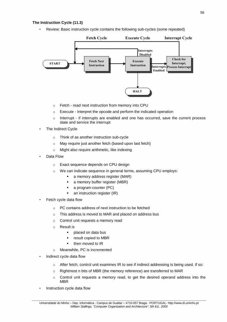
58
Universidade do Minho – Dep. Informática - Campus de Gualtar – 4710-057 Braga - PORTUGAL- http://www.di.uminho.pt William Stallings, “Computer Organization and Architecture”, 5th Ed., 2000
The Instruction Cycle (11.3)
• Review: Basic instruction cycle contains the following sub-cycles (some repeated)
o Fetch - read next instruction from memory into CPU
o Execute - Interpret the opcode and perform the indicated operation
o Interrupt - if interrupts are enabled and one has occurred, save the current process state and service the interrupt
• The Indirect Cycle
o Think of as another instruction sub-cycle
o May require just another fetch (based upon last fetch)
o Might also require arithmetic, like indexing
• Data Flow
o Exact sequence depends on CPU design
o We can indicate sequence in general terms, assuming CPU employs: § a memory address register (MAR) § a memory buffer register (MBR) § a program counter (PC) § an instruction register (IR)
• Fetch cycle data flow
o PC contains address of next instruction to be fetched
o This address is moved to MAR and placed on address bus
o Control unit requests a memory read
o Result is § placed on data bus § result copied to MBR § then moved to IR
o Meanwhile, PC is incremented
• Indirect cycle data flow
o After fetch, control unit examines IR to see if indirect addressing is being used. If so:
o Rightmost n bits of MBR (the memory reference) are transferred to MAR
o Control unit requests a memory read, to get the desired operand address into the MBR
• Instruction cycle data flow
59
Universidade do Minho – Dep. Informática - Campus de Gualtar – 4710-057 Braga - PORTUGAL- http://www.di.uminho.pt William Stallings, “Computer Organization and Architecture”, 5th Ed., 2000
o Not simple and predictable, like other cycles
o Takes many forms, since form depends on which of the various machine instructions is in the IR
o May involve § transferring data among registers § read or write from memory or I/O § invocation of the ALU
• Interrupt cycle data flow
o Current contents of PC must be saved (for resume after interrupt), so PC is transferred to MBR to be written to memory
o Save location’s address (such as a stack ptr) is loaded into MAR from the control unit
o PC is loaded with address of interrupt routine (so next instruction cycle will begin by fetching appropriate instruction)
Instruction Pipelining (11.4)
• Concept is similar to a manufacturing assembly line
o Products at various stages can be worked on simultaneously
o Also referred to as pipelining, because, as in a pipeline, new inputs are accepted at one end before previously accepted inputs appear as outputs at the other end
• Consider subdividing instruction processing into two stages:
o Fetch instruction
o Execute instruction
• During execution, there are times when main memory is not being accessed.
• During this time, the next instruction could be fetched and buffered (called instruction prefetch or fetch overlap).
• If the Fetch and Execute stages were of equal duration, the instruction cycle time would be halved.
• However, doubling of execution time is unlikely because:
o Execution time is generally longer than fetch time (it will also involve reading and storing operands, in addition to operation execution)
o A conditional branch makes the address of the next instruction to be fetched unknown (although we can minimize this problem by fetching the next sequential instruction anyway)
• To gain further speedup, the pipeline must have more stages. Consider the following decomposition of instruction processing:
o Fetch Instruction (FI)
o Decode Instruction (DI) - determine opcode and operand specifiers
o Calculate Operands (CO) - calculate effective address of each source operand
o Fetch Operands (FO)
o Execute Instruction (EI)
o Write Operand (WO)
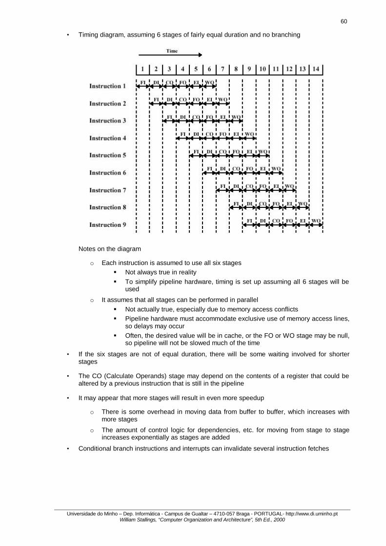
60
Universidade do Minho – Dep. Informática - Campus de Gualtar – 4710-057 Braga - PORTUGAL- http://www.di.uminho.pt William Stallings, “Computer Organization and Architecture”, 5th Ed., 2000
• Timing diagram, assuming 6 stages of fairly equal duration and no branching
Notes on the diagram
o Each instruction is assumed to use all six stages § Not always true in reality § To simplify pipeline hardware, timing is set up assuming all 6 stages will be
used
o It assumes that all stages can be performed in parallel § Not actually true, especially due to memory access conflicts § Pipeline hardware must accommodate exclusive use of memory access lines,
so delays may occur § Often, the desired value will be in cache, or the FO or WO stage may be null,
so pipeline will not be slowed much of the time
• If the six stages are not of equal duration, there will be some waiting involved for shorter stages
• The CO (Calculate Operands) stage may depend on the contents of a register that could be altered by a previous instruction that is still in the pipeline
• It may appear that more stages will result in even more speedup
o There is some overhead in moving data from buffer to buffer, which increases with more stages
o The amount of control logic for dependencies, etc. for moving from stage to stage increases exponentially as stages are added
• Conditional branch instructions and interrupts can invalidate several instruction fetches
61
Universidade do Minho – Dep. Informática - Campus de Gualtar – 4710-057 Braga - PORTUGAL- http://www.di.uminho.pt William Stallings, “Computer Organization and Architecture”, 5th Ed., 2000
Dealing with Branches
• A variety of approaches have been taken for dealing with conditional branches:
o Multiple Streams § Instead of choosing one of the two instructions, replicate the initial portions of
the pipeline and allow it to fetch both instructions, making use of two streams. § Problems: § Contention delays for access to registers and memory § Additional branch instructions may enter either stream of the pipeline before
the original branch decision is resolved § Examples: IBM 370/168 and IBM 3033
o Prefetch Branch Target § The target of the branch is prefetched, in addition to the instruction following
the branch. The target is saved until the branch instruction is executed, so it is available without fetching at that time.
§ Example: IBM 360/91
o Loop Buffer § A small, very-high-speed memory maintained by the instruction fetch stage of
the pipeline § contains the n most recently fetched instructions, in sequence § if a branch is to be taken, the buffer is checked first and the next
instruction fetched from it instead of memory § Benefits
§ It will often contain an instruction sequentially ahead of the current instruction, which can be used for prefetching
§ If a branch occurs to a target just a few locations ahead of the branch instruction, the target may already be in the buffer (especially useful for IF-THEN and IF-THEN-ELSE sequences)
§ As implied by the name, if the buffer is large enough to contain all the instructions in a loop, they will only have to be fetched from memory once for all the consecutive iterations of that loop
§ Similar in principle to an instruction cache, but § it only holds instructions in sequence § smaller and thus lower cost
§ Examples: CDC Star-100, 6600, 7600 and CRAY-1
o Branch Prediction § Try to predict which branch will be taken, and prefetch that instruction § Static techniques
§ Predict Never Taken § Assume that the branch will not be taken and continue to
fetch in sequence § Examples: Motorola 68020 and VAX 11/780
§ Predict Always Taken § Assume that the branch will always be taken, and always
fetch the branch target § Studies show that conditional branches are taken more than
50% of the time NOTE: Prefetching the branch target is more likely to cause a page fault; so paged machines may employ an avoidance mechanism to reduce this penalty.
§ Predict by Opcode § Assume that the branch will be taken for certain branch
opcodes and not for others § Studies report success rates of greater than 75%
62
Universidade do Minho – Dep. Informática - Campus de Gualtar – 4710-057 Braga - PORTUGAL- http://www.di.uminho.pt William Stallings, “Computer Organization and Architecture”, 5th Ed., 2000
§ Dynamic Techniques § Taken/Not Taken Switch
§ Assume that future executions of the same branch instruction will branch the same way
§ Associate one or two extra bits with the branch instruction in high-speed memory (instruction cache or loop buffer) indicating whether it was taken the last one or two times
§ Two bits allow events like loops to only cause one wrong prediction instead of two
§ Example: IBM 3090/400 § Branch History Table
§ Solves problem with Taken/Not Taken Switch, to wit: If decision is made to take the branch, the target instruction cannot be fetched until the target address is decoded
§ Branch History Table is a small cache memory associated with the instruction fetch stage of the pipeline. Each entry has: >> the address of a branch instruction >> some number of history bits that record the state of use of that instruction >> effective address of target instruction (already calculated) or the target instruction itself
§ Example: AMD29000
o Delayed Branch § Sometimes code can be optimized so that branch instructions can occur later
than originally specified § Allows pipeline to stay full longer before potential flushing § More detail in chapter 12 (RISC)
Intel 80486 Pipelining (11.5)
o Uses a 5-stage pipeline § Fetch - instructions are prefetched into 1 of 2 16-byte prefetch buffers.
§ Buffers are filled as soon as old data is consumed by instruction decoder
§ Instructions are variable length (1-11 bytes) § On average, about 5 instructions are fetched with each 16-byte load § Independent of rest of pipeline
§ Decode Stage 1 § Opcode and addressing mode info is decoded § This info always occurs in first 3 bytes of instruction
§ Decode Stage 2 § Expands each opcode into control signals for the ALU § Computation of more complex addressing modes
§ Execute § ALU operations § cache access § register update
§ Write Back § May not be needed § Updates registers and status flags modified during Execute stage § If current instruction updates memory, the computed value is sent to
the cache and to the bus-interface write buffers at the same time
o With 2 decode stages, can sustain a throughput of close to 1 instruction per clock cycle (complex instructions and conditional branches cause slowdown)
63
Universidade do Minho – Dep. Informática - Campus de Gualtar – 4710-057 Braga - PORTUGAL- http://www.di.uminho.pt William Stallings, “Computer Organization and Architecture”, 5th Ed., 2000
III. THE CENTRAL PROCESSING UNIT.
8. ... 9. ... 10. ... 11. ... 12. Reduced Instruction Set Computers (RISCs). (5-Jan-01)
Introduction
• RISC is one of the few true innovations in computer organization and architecture in the last 50 years of computing.
• Key elements common to most designs:
o A limited and simple instruction set
o A large number of general purpose registers, or the use of compiler technology to optimize register usage
o An emphasis on optimizing the instruction pipeline
Instruction Execution Characteristics (12.1)
• Overview
o Semantic Gap - the difference between the operations provided in high-level languages and those provided in computer architecture
o Symptoms of the semantic gap: § Execution inefficiency § Excessive machine program size § Compiler complexity
o New designs had features trying to close gap: § Large instruction sets § Dozens of addressing modes § Various HLL statements in hardware
o Intent of these designs: § Make compiler-writing easier § Improve execution efficiency by implementing complex sequences of
operations in microcode § Provide support for even more complex and sophisticated HLL's
o Concurrently, studies of the machine instructions generated by HLL programs § Looked at the characteristics and patterns of execution of such instructions § Results lead to using simpler architectures to support HLL's, instead of more
complex
o To understand the reasoning of the RISC advocates, we look at study results on 3 main aspects of computation: § Operations performed - the functions to be performed by the CPU and its
interaction with memory. § Operands used - types of operands and their frequency of use. Determine
memory organization and addressing modes. § Execution Sequencing - determines the control and pipeline organization.
o Study results are based on dynamic measurements (during program execution), so that we can see effect on performance
64
Universidade do Minho – Dep. Informática - Campus de Gualtar – 4710-057 Braga - PORTUGAL- http://www.di.uminho.pt William Stallings, “Computer Organization and Architecture”, 5th Ed., 2000
• Operations
o Simple counting of statement frequency indicates that assignment (data movement) predominates, followed by selection/iteration.
o Weighted studies show that call/return actually accounts for the most work
o Target architectural organization to support these operations well
o Patterson study also looked at dynamic frequency of occurrence of classes of variables. Results showed a preponderance of references to highly localized scalars: § Majority of references are to simple scalars § Over 80% of scalars were local variables § References to arrays/structures require a previous ref to their index or pointer,
which is usually a local scalar
• Operands
o Another study found that each instruction (DEC-10 in this case) references 0.5 operands in memory and 1.4 registers.
o Implications: § Need for fast operand accessing § Need for optimized mechanisms for storing and accessing local scalar
variables
• Execution Sequencing
o Subroutine calls are the time-consuming operation in HLL's
o Minimize their impact by § Streamlining the parameter passing § Efficient access to local variables § Support nested subroutine invocation
o Statistics § 98% of dynamically called procedures passed fewer than 6 parameters § 92% use less than 6 local scalar variables § Rare to have long sequences of subroutine calls followed by returns (e.g., a
recursive sorting algorithm) § Depth of nesting was typically rather low
• Implications
o Reducing the semantic gap through complex architectures may not be the most efficient use of system hardware
o Optimize machine design based on the most time-consuming tasks of typical HLL programs
o Use large numbers of registers § Reduce memory reference by keeping variables close to CPU (more register
refs instead) § Streamlines instruction set by making memory interactions primarily loads and
stores
o Pipeline design § Minimize impact of conditional branches
o Simplify instruction set rather than make it more complex
65
Universidade do Minho – Dep. Informática - Campus de Gualtar – 4710-057 Braga - PORTUGAL- http://www.di.uminho.pt William Stallings, “Computer Organization and Architecture”, 5th Ed., 2000
Large Register Files (12.2)
• How can we make programs use registers more often?
o Software - optimizing compilers § Compiler attempts to allocate registers to those variables that will be used
most in a given time period § Requires sophisticated program-analysis algorithms
o Hardware § Make more registers available, so that they'll be used more often by ordinary
compilers § Pioneered at Berkeley by first commercial RISC product, the Pyramid
• Register Windows
o Naively adding registers will not effectively reduce need to access memory § Since most operand references are to local scalars, obviously store them in
registers, with maybe a few for global variables § Problem: Definition of local changes with each procedure call and return
(which happen a lot!) § On call, locals must be moved from registers to memory to make room for
called subroutine § Parameters must be passed § On return, parent variables must move back to registers
o Remember study results: § A typical procedure uses only a few passed parameters and local
variables § The depth of procedure activation fluctuates within a relatively narrow
range
o So: § Use multiple small sets of registers, each assigned to a different
procedure § A procedure call automatically switches the CPU to use a different fixed-
size window of registers (no saving registers in memory!) § Windows for adjacent procedures are overlapped to allow parameter
passing
o Since there is a limit to number of windows, we use a circular buffer of windows § Only hold the most recent procedure activations in register windows § Older activations must be saved to memory and later restored
§ An N-window register file can hold only N-1 procedure activations § One study found that with 8 windows, a save or restore is needed
on only 1% of calls or returns
• Global variables
o Could just use memory, but would be inefficient for frequently used globals
o Incorporate a set of global registers in the CPU. Then, the registers available to a procedure would be split: § some would be the global registers § the rest would be in the current window.
o Hardware would have to also: § decide which globals to put in registers § accommodate the split in register addressing
66
Universidade do Minho – Dep. Informática - Campus de Gualtar – 4710-057 Braga - PORTUGAL- http://www.di.uminho.pt William Stallings, “Computer Organization and Architecture”, 5th Ed., 2000
• Large Register File vs. Cache
o Why not just build a big cache? Answer not clear cut § Window holds all local scalars § Cache holds selection of recently used data § Cache can be forced to hold data it never uses (due to block transfers) § Current data in cache can be swapped out due to accessing scheme used § Cache can easily store global and local variables § Addressing registers is cleaner and faster
Compiler-Based Register Optimization (12.3)
• In this case, the number of registers is small compared to the large register file implementation
• The compiler is responsible for managing the use of the registers
• Compiler must map the current and projected use of variables onto the available registers
o Similar to a graph coloring problem
o Form a graph with variables as nodes and edges that link variables that are active at the same time
o Color the graph with as many colors as you have registers
o Variables not colored must be stored in memory Reduced Instruction Set Architecture (12.4)
• Why CISC?
o CISC trends to richer instruction sets § More instructions § More complex instructions
o Reasons § To simplify compilers § To improve performance
• Are compilers simplified?
o Assertion: If there are machine instructions that resemble HLL statements, compiler construction is simpler
o Counter-arguments: § Complex machine instructions are often hard to exploit because the compiler
must find those cases that fit the construct § Other compiler goals
§ Minimizing code size § Reducing instruction execution count § Enhancing pipelining
are more difficult with a complex instruction set § Studies show that most instructions actually produced by CISC compilers are
the relatively simple ones
• Is performance improved?
o Assertion: Programs will be smaller and they will execute faster § Smaller programs save memory § Smaller programs have fewer instructions, requiring less instruction fetching § Smaller programs occupy fewer pages in a paged environment, so have
fewer page faults
67
Universidade do Minho – Dep. Informática - Campus de Gualtar – 4710-057 Braga - PORTUGAL- http://www.di.uminho.pt William Stallings, “Computer Organization and Architecture”, 5th Ed., 2000
o Counter-arguments: § Inexpensive memory makes memory savings less compelling
• CISC programs may be shorter, but bits used for each instruction are more, so total memory used may not be smaller
o Opcodes require more bits
o Operands require more bits because they are usually memory addresses, as opposed to register identifiers (which are the usual case for RISC)
• The entire control unit must be more complex to accommodate seldom used complex operations, so even the more often-used simple operations take longer
• The speedup for complex instructions may be mostly due to their implementation as simpler instructions in microcode, which is similar to the speed of simpler instructions in RISC (except that the CISC designer must decide a priori which instructions to speed up in this way)
• Characteristics of RISC Architectures
o One instruction per cycle § A machine cycle is defined by the time it takes to fetch two operands from
registers, perform and ALU operation, and store the result in a register § RISC machine instructions should be no more complicated than, and execute
about as fast as microinstructions on a CISC machine § No microcoding needed, and simple instructions will execute faster than their
CISC equivalents due to no access to microprogram control store.
o Register-to-register operations § Only simple LOAD and STORE operations access memory § Simplifies instruction set and control unit
§ Ex. Typical RISC has 2 ADD instructions § Ex. VAX has 25 different ADD instructions
§ Encourages optimization of register use
o Simple addressing modes § Almost all instructions use simple register addressing § A few other modes, such as displacement and PC relative, may be provided § More complex addressing is implemented in software from the simpler ones § Further simplifies instruction set and control unit
o Simple instruction formats § Only a few formats are used
§ Further simplifies the control unit § Instruction length is fixed and aligned on word boundaries
§ Optimizes instruction fetching § Single instructions don't cross page boundaries
§ Field locations (especially the opcode) are fixed § Allows simultaneous opcode decoding and register operand access
• Potential benefits
o More effective optimizing compilers
o Simpler control unit can execute instructions faster than a comparable CISC unit
o Instruction pipelining can be applied more effectively with a reduced instruction set
o More responsiveness to interrupts § They are checked between rudimentary operations § No need for complex instruction restarting mechanisms
• VLSI implementation
68
Universidade do Minho – Dep. Informática - Campus de Gualtar – 4710-057 Braga - PORTUGAL- http://www.di.uminho.pt William Stallings, “Computer Organization and Architecture”, 5th Ed., 2000
o Requires less "real estate" for control unit (6% in RISC I vs. about 50% for CISC microcode store)
o Less design and implementation time RISC Pipelining (12.5)
• The simplified structure of RISC instructions allows us to reconsider pipelining
o Most instructions are register-to-register, so an instruction cycle has 2 phases § I: Instruction Fetch § E: Execute (an ALU operation w/ register input and output)
o For load and store operations, 3 phases are needed § I: Instruction fetch § E: Execute (actually memory address calculation) § D: Memory (register-to-memory or memory-to-register)
• Since the E phase usually involves an ALU operation, it may be longer than the other phases. In this case, we can divide it into 2 sub phases:
o E1: Register file read
o E2: ALU operation and register write Optimization of Pipelining
• Delayed Branch
o We've seen that data and branch dependencies reduce the overall execution rate in the pipeline
o Delayed branch makes use of a branch that does not take effect until after the execution of the following instruction § Note that the branch "takes effect" during its execution phase § So, the instruction location immediately following the branch is called the
delay slot § This is because the instruction fetching order is not affected by the branch
until the instruction after the delay slot § Rather than wasting an instruction with a NOOP, it may be possible to move
the instruction preceding the branch to the delay slot, while still retaining the original program semantics.
• Conditional branches
o If the instruction immediately preceding the branch cannot alter the branch condition, this optimization can be applied
o Otherwise a NOOP delay is still required.
o Experience with both the Berkeley RISC and IBM 801 systems shows that a majority of conditional branches can be optimized this way.
• Delayed Load
o On load instructions, the register to be loaded is locked by the processor
o The processor continues execution of the instruction stream until reaching an instruction needing a locked register
o It then idles until the load is complete
o If load takes a specific maximum number of clock cycles, it may be possible to rearrange instructions to avoid the idle.
Superpipelining
• A superpipelined architecture is one that makes use of more, and finer-grained, pipeline stages.
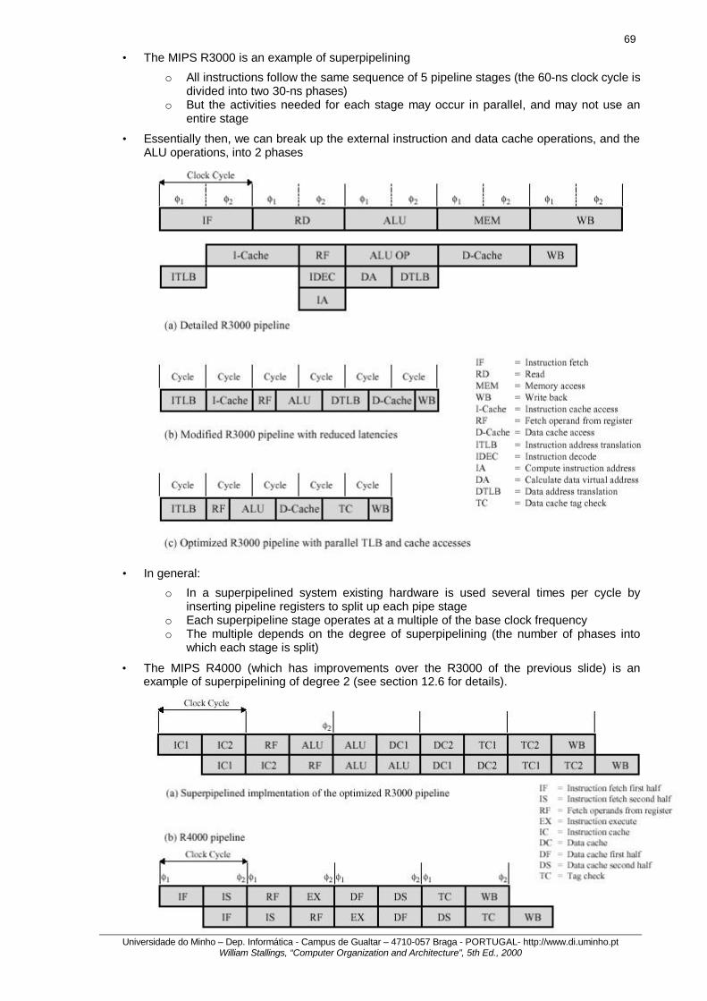
69
Universidade do Minho – Dep. Informática - Campus de Gualtar – 4710-057 Braga - PORTUGAL- http://www.di.uminho.pt William Stallings, “Computer Organization and Architecture”, 5th Ed., 2000
• The MIPS R3000 is an example of superpipelining
o All instructions follow the same sequence of 5 pipeline stages (the 60-ns clock cycle is divided into two 30-ns phases)
o But the activities needed for each stage may occur in parallel, and may not use an entire stage
• Essentially then, we can break up the external instruction and data cache operations, and the ALU operations, into 2 phases
• In general:
o In a superpipelined system existing hardware is used several times per cycle by inserting pipeline registers to split up each pipe stage
o Each superpipeline stage operates at a multiple of the base clock frequency o The multiple depends on the degree of superpipelining (the number of phases into
which each stage is split)
• The MIPS R4000 (which has improvements over the R3000 of the previous slide) is an example of superpipelining of degree 2 (see section 12.6 for details).
70
Universidade do Minho – Dep. Informática - Campus de Gualtar – 4710-057 Braga - PORTUGAL- http://www.di.uminho.pt William Stallings, “Computer Organization and Architecture”, 5th Ed., 2000
The RISC vs. CISC Controversy (12.8)
• In spite of the apparent advantages of RISC, it is still an open question whether the RISC approach is demonstrably better.
• Studies to compare RISC to CISC are hampered by several problems (as of the textbook writing):
o There is no pair of RISC and CISC machines that are closely comparable
o No definitive set of test programs exist.
o It is difficult to sort out hardware effects from effects due to skill in compiler writing.
• Most of the comparative analysis on RISC has been done on “toy” machines, rather than commercial products.
• Most commercially available “RISC” machines possess a mixture of RISC and CISC characteristics.
• The controversy has died down to a great extent
o As chip densities and speeds increase, RISC systems have become more complex
o To improve performance, CISC systems have increased their number of general-purpose registers and increased emphasis on instruction pipeline design.
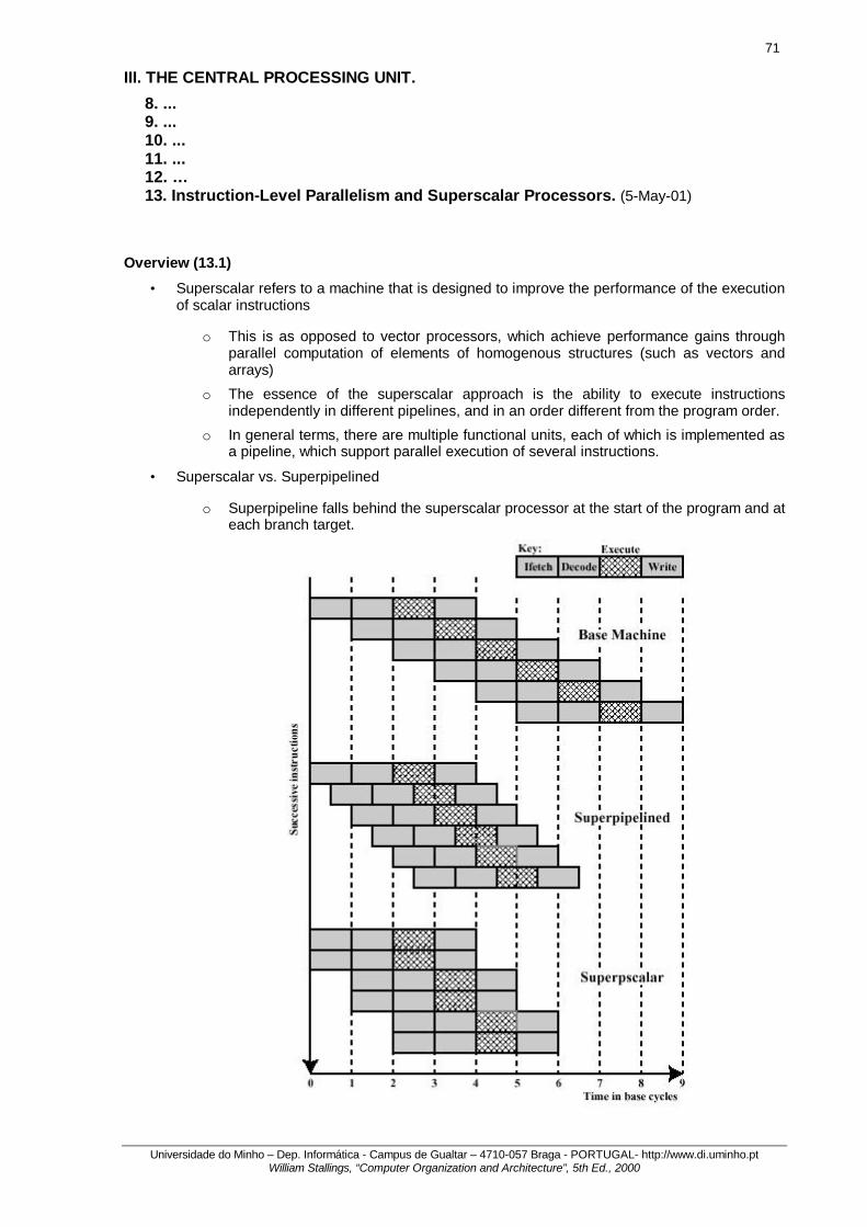
71
Universidade do Minho – Dep. Informática - Campus de Gualtar – 4710-057 Braga - PORTUGAL- http://www.di.uminho.pt William Stallings, “Computer Organization and Architecture”, 5th Ed., 2000
III. THE CENTRAL PROCESSING UNIT.
8. ... 9. ... 10. ... 11. ... 12. … 13. Instruction-Level Parallelism and Superscalar Processors. (5-May-01)
Overview (13.1)
• Superscalar refers to a machine that is designed to improve the performance of the execution of scalar instructions
o This is as opposed to vector processors, which achieve performance gains through parallel computation of elements of homogenous structures (such as vectors and arrays)
o The essence of the superscalar approach is the ability to execute instructions independently in different pipelines, and in an order different from the program order.
o In general terms, there are multiple functional units, each of which is implemented as a pipeline, which support parallel execution of several instructions.
• Superscalar vs. Superpipelined
o Superpipeline falls behind the superscalar processor at the start of the program and at each branch target.
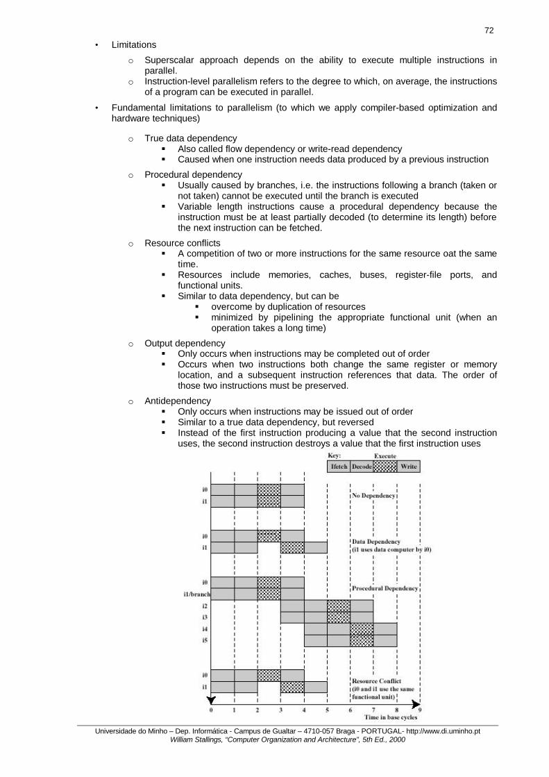
72
Universidade do Minho – Dep. Informática - Campus de Gualtar – 4710-057 Braga - PORTUGAL- http://www.di.uminho.pt William Stallings, “Computer Organization and Architecture”, 5th Ed., 2000
• Limitations
o Superscalar approach depends on the ability to execute multiple instructions in parallel.
o Instruction-level parallelism refers to the degree to which, on average, the instructions of a program can be executed in parallel.
• Fundamental limitations to parallelism (to which we apply compiler-based optimization and hardware techniques)
o True data dependency § Also called flow dependency or write-read dependency § Caused when one instruction needs data produced by a previous instruction
o Procedural dependency § Usually caused by branches, i.e. the instructions following a branch (taken or
not taken) cannot be executed until the branch is executed § Variable length instructions cause a procedural dependency because the
instruction must be at least partially decoded (to determine its length) before the next instruction can be fetched.
o Resource conflicts § A competition of two or more instructions for the same resource oat the same
time. § Resources include memories, caches, buses, register-file ports, and
functional units. § Similar to data dependency, but can be
§ overcome by duplication of resources § minimized by pipelining the appropriate functional unit (when an
operation takes a long time)
o Output dependency § Only occurs when instructions may be completed out of order § Occurs when two instructions both change the same register or memory
location, and a subsequent instruction references that data. The order of those two instructions must be preserved.
o Antidependency § Only occurs when instructions may be issued out of order § Similar to a true data dependency, but reversed § Instead of the first instruction producing a value that the second instruction
uses, the second instruction destroys a value that the first instruction uses


![Sistemi Operativi [William Stallings]](https://static.fdocuments.us/doc/165x107/543cd117b1af9fc42e8b4811/sistemi-operativi-william-stallings.jpg)