Wideband Current Transducer for Measuring AC … · 1776 IEEE TRANSACTIONS ON POWER ELECTRONICS,...
13
Wideband Current Transducer for Measuring AC Signals With Limited DC Offset Michael Hartmann, Student Member, IEEE, Juergen Biela, Member, IEEE, Hans Ertl, Member, IEEE, and Johann W. Kolar, Senior Member, IEEE „This material is posted here with permission of the IEEE. Such permission of the IEEE does not in any way imply IEEE endorsement of any of ETH Zürich’s products or services. Internal or personal use of this material is permitted. However, permission to reprint/republish this material for advertising or promo- tional purposes or for creating new collective works for resale or redistribution must be obtained from the IEEE by writing to [email protected]. By choosing to view this document you agree to all provisions of the copyright laws protecting it.”
Transcript of Wideband Current Transducer for Measuring AC … · 1776 IEEE TRANSACTIONS ON POWER ELECTRONICS,...

Wideband Current Transducer for Measuring AC Signals With Limited DC Offset
Michael Hartmann, Student Member, IEEE, Juergen Biela, Member, IEEE, Hans Ertl, Member, IEEE,
and Johann W. Kolar, Senior Member, IEEE „This material is posted here with permission of the IEEE. Such permission of the IEEE does not in any way imply IEEE endorsement of any of ETH Zürich’s products or services. Internal or personal use of this material is permitted. However, permission to reprint/republish this material for advertising or promo-tional purposes or for creating new collective works for resale or redistribution must be obtained from the IEEE by writing to [email protected]. By choosing to view this document you agree to all provisions of the copyright laws protecting it.”
1776 IEEE TRANSACTIONS ON POWER ELECTRONICS, VOL. 24, NO. 7, JULY 2009
Wideband Current Transducer for Measuring ACSignals With Limited DC Offset
Michael Hartmann, Student Member, IEEE, Juergen Biela, Member, IEEE, Hans Ertl, Member, IEEE,and Johann W. Kolar, Senior Member, IEEE
Abstract—In many applications, a current measurement thatcan measure ac currents with dc offset is required. This is notpossible using conventional current transformers (CTs) due to thecore saturation because of the dc offset. In this paper, a new sen-sor concept is presented, which consists of a wideband CT and ademagnetizing circuit. The sensor concept is capable of measuringac currents with dc offset, which have periodic zero crossings, asgiven in power-factor-corrected (PFC) circuits. Using the demag-netization circuit, the core is actively reset during the zero crossingintervals. The operation principle and design equations are dis-cussed in detail in this paper. For validating the presented concept,three sensors have been built using different core materials, andmeasurements of the transfer functions as well as operation in aPFC system are presented. A bandwidth from dc up to 20 MHz hasbeen achieved.
Index Terms—Current measurement, current transformer (CT),nanocrystalline material.
I. INTRODUCTION
AN INCREASING number of power electronic systemsconnected to the power grid, such as input stages of tele-
com power supplies [1], [2], front-end systems of drives [3],or power electronics for renewable energy sources [4], [5], arerealized with active rectifier circuit topologies. In order to min-imize the influence on the mains, sinusoidal input currents anda unity power factor are required. A current controller is used toachieve these requirements, for which the input currents mustbe measured (cf., Fig. 1). Additionally, a superimposed volt-age or load regulation is applied, which is not shown in Fig. 1for simplicity. In contrast to single-phase systems with a typ-ical power level below 1 kW, where often shunt resistors areused for current measurement, a galvanically isolated currentmeasurement is required for higher power levels, where usu-ally three-phase systems are utilized. Such a concept offers theadvantage of lower losses, since usually no shunt resistors areused, and measurement signals that can be processed directlyby the digital signal processor. Therefore, it is very importantthat the current sensor should also measure dc currents besidesthe ac component in order to guarantee dc-free mains currents.
Manuscript received August 29, 2008; revised November 28, 2008. Currentversion published July 29, 2009. Recommended for publication by AssociateEditor C. R. Sullivan.
M. Hartmann, J. Biela, and J. W. Kolar are with the Power Electronic Sys-tems Laboratory, Swiss Federal Institute of Technology (ETH) Zurich, CH-8092Zurich, Switzerland (e-mail: [email protected]; [email protected];[email protected]).
H. Ertl is with the Power Electronics Section, Vienna University of Technol-ogy, A-1040 Vienna, Austria (e-mail: [email protected]).
Digital Object Identifier 10.1109/TPEL.2009.2017263
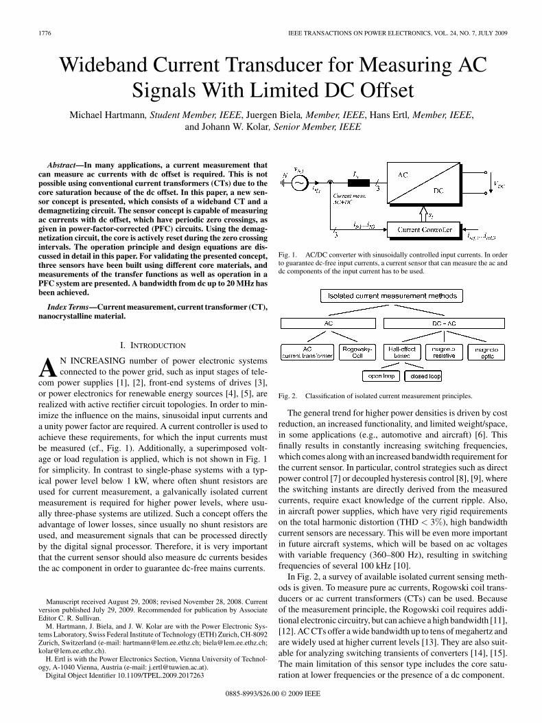
Fig. 1. AC/DC converter with sinusoidally controlled input currents. In orderto guarantee dc-free input currents, a current sensor that can measure the ac anddc components of the input current has to be used.
Fig. 2. Classification of isolated current measurement principles.
The general trend for higher power densities is driven by costreduction, an increased functionality, and limited weight/space,in some applications (e.g., automotive and aircraft) [6]. Thisfinally results in constantly increasing switching frequencies,which comes along with an increased bandwidth requirement forthe current sensor. In particular, control strategies such as directpower control [7] or decoupled hysteresis control [8], [9], wherethe switching instants are directly derived from the measuredcurrents, require exact knowledge of the current ripple. Also,in aircraft power supplies, which have very rigid requirementson the total harmonic distortion (THD < 3%), high bandwidthcurrent sensors are necessary. This will be even more importantin future aircraft systems, which will be based on ac voltageswith variable frequency (360–800 Hz), resulting in switchingfrequencies of several 100 kHz [10].
In Fig. 2, a survey of available isolated current sensing meth-ods is given. To measure pure ac currents, Rogowski coil trans-ducers or ac current transformers (CTs) can be used. Becauseof the measurement principle, the Rogowski coil requires addi-tional electronic circuitry, but can achieve a high bandwidth [11],[12]. AC CTs offer a wide bandwidth up to tens of megahertz andare widely used at higher current levels [13]. They are also suit-able for analyzing switching transients of converters [14], [15].The main limitation of this sensor type includes the core satu-ration at lower frequencies or the presence of a dc component.
0885-8993/$26.00 © 2009 IEEE

HARTMANN et al.: WIDEBAND CURRENT TRANSDUCER FOR MEASURING AC SIGNALS WITH LIMITED DC OFFSET 1777
DC and ac currents can be measured using Hall-effect-basedsensors, transducers based on the magnetoresistive effect or forhigh voltage, and current levels by magnetooptic sensors. Op-tical current transducers [16] are based on the Faraday effect,and basically offer a wide bandwidth. Their main applicationareas are high-voltage power distribution systems. The essen-tial drawbacks of this sensor type are its nonlinearity and thehuge temperature dependency. Current sensors based on themagnetoresistive effect are commercially available for severalyears [17]. They are very attractive for integration in power elec-tronic systems. However, the bandwidth of this sensor is limitedto approximately 1 MHz due to the physical limitations of themagnetoresistive sensor element [18].
Hall effect current transducers are based on a Hall-type sens-ing device located in the air gap of a magnetic core to detectdc + ac components up to several 10 kHz. In closed-loop con-figuration, the Hall element is used to compensate the low-frequency flux in the core in combination with an amplifierfeedback path. In open-loop configuration, the Hall device isused for sensing the current components directly, leading to areduced linearity in comparison to a closed-loop sensor. Bothconfigurations can be combined with a CT that has to be matchedwith the ac performance of the Hall element. This concepts en-ables high-performance current sensors with a bandwidth fromdc up to 30 MHz [19].
The Hall element has also been successfully combined with aRogowski coil, which is also known as HOKA [20]. To insert theHall element in the magnetic path, a core with an air gap is re-quired, which may be a complex and expensive production step.Additionally, two sensor elements are needed for these trans-ducer types. Furthermore, several systems have been reportedto measure dc currents with an ac CT using the nonlinear magne-tizing curve of the CT [21], [22]. Unfortunately, these conceptshave a very limited upper bandwidth. Several other core flux can-cellation techniques were reported in the literature [23], [24];however, they show limited upper bandwidth and higher com-plexity. Pulse currents, as they occur in the switch or in the diodeof a dc/dc converter, can be measured using a CT [25], if theCT is demagnetized periodically between the current pulses.As shown in [26], the system behavior of these circuits canbe improved by replacing the burden resistance with an activestage (active loading) and applying synchronous rectification.In [27], additional reset voltage feedback is used to determine anecessary compensation voltage for the magnetic flux. If pulsecurrent CTs are arranged in a dual transformer arrangement,such CTs can be used for inductor current measurements ofa power-factor-corrected (PFC) stage [28]. However, two CTsare needed (one to sense the switch current and the other tosense the current through the boost diode) and their output sig-nal has to be combined, which may be difficult in a practicalrealization.
Since the known concepts have limitations because of theirbandwidth and/or requirement of complex core geometries ormeasurement electronics, a new and simple concept for ac anddc current measurement in active rectifier systems, which doesnot require additional sensor elements for detecting the magneticflux, is proposed in this paper.
In the considered active rectifiers, the input currents haveapproximately a sinusoidal shape and therefore show zerocrossings at fixed time intervals. Furthermore, the measure-ment signals of the input currents are only required during thepositive/negative half-wave between the zero crossings. There-fore, the new sensor consists of a conventional CT, which doesnot saturate during the half-wave of the input current and mea-sures the ac and dc components of the input current during thistime. During the zero crossings, the current is kept for a shorttime at zero by the current controller, and the magnetic core canbe reset/demagnetized so that the flux is zero at the beginning ofthe next half-wave and can measure the current during the nexthalf-wave (cf., Fig. 3).
Since there are already distortions at the zero crossings ofthe input currents of a PFC, which can not be avoided com-pletely [29], the short time for demagnetizing the current sensorsdoes not cause noticeable additional distortion. Consequently,the CT in combination with minor extensions in the currentcontroller can be used for measuring the ac as well as the dccomponents of the input current without any additional sensorelement. Because the voltage does not need to be in phase withthe input current, the proposed sensor concept is not limitedto only PFC applications. The sensor concept requires that thecurrent to be measured periodically gets zero for a certain timeinterval and can therefore be used in all applications where thisrequirement is fulfilled.
II. PRINCIPLE OF OPERATION
In Fig. 3(a), the schematic of the proposed current sensorfor a single-phase PFC circuit is given, where the current sen-sor is located on the ac side of the active rectifier. Therefore,the current sensor using a CT consisting of a transformer andthe burden resistance RB is extended by the switch S2 , twoZener diodes, and some control logic implemented in the (dig-ital) current controller. If S2 is closed, voltage vi,meas is equalto the voltage across the burden resistor, which is proportional tothe input current: vi,meas = iN /N RB . As shown in Fig. 3(b),the magnetizing current im of the CT raises during the half-wave of the input current (details are discussed in the followingsection). If a sinusoidal current iN causing a sinusoidal voltagevi,meas is assumed, the magnetizing current at instant T/2 canbe calculated approximately by
im =RB
Lm
∫ T /2
0
IN
Nsin(ωτ)dτ =
2IN RB
Lm Nω. (1)
In case of a purely sinusoidal current iN , the magnetizing currentim will be zero after a full period T . In Fig. 3(b), a small dccomponent is assumed, hence a small value of im will remainafter one period T . Without any demagnetizing, im would raisemore and more in case the input current has a dc component,and the core of the CT would saturate after some period.
By demagnetizing the CT at each zero crossing of the primarycurrent, the dc component does not lead to a core saturation,which can be measured by comparing the positive and negativehalf-wave. For demagnetizing the core, the zero crossing of iNis detected, and the pulsewidth modulation (PWM) signal of the

1778 IEEE TRANSACTIONS ON POWER ELECTRONICS, VOL. 24, NO. 7, JULY 2009
Fig. 3. Schematic of the proposed current sensor consisting of a CT and a demagnetizing circuit for (a) a single-phase PFC. (b) Demagnetization concept withdemagnetization after a full period and after a half-period. (c) One phaseleg of the realization for a three-phase active rectifier (for example, a VIENNA rectifiercircuit is shown).
PFC switch S1 is set to zero, so that the primary current of theCT stays zero. At the same time, S2 is opened (vi,meas is held tozero by the burden resistor RB ) and the magnetizing current ofthe CT now flows via the Zener diodes. Since the Zener voltageof the diodes is much higher than the magnitude of vi,meas , thetime to demagnetize the core is very short. After the CT is fullydemagnetized, S2 can be closed and the PWM signal generatedfrom the current controller is reapplied to S1 . The time needed todemagnetize the current sensor tdemag can be calculated easilyusing the approximation
Uz = Lmdimdt
≈ Lm∆im∆t
(2)
which leads to
tdemag =RB
NUz
∫ tm e a s
0iN (τ)dτ (3)
where tmeas denotes the measuring time until the sensor is de-magnetized. As the phase current of the rectifier is forced to zeroduring tdemag , the sensor concept causes current distortions inthe input current iN . Since several other effects, such as cuspdistortion [30] or discontinuous-mode (DCM) of operation ofthe boost inductor [31], already generate zero crossing distor-tions, the distortions caused by the proposed sensor concept arenot significant. In Fig. 4, the harmonics of an average current-mode-controlled 1-kW single-phase PFC prototype with andwithout the new sensor concept are shown. As it can be seen,no noticeable additional harmonics are caused by the demagne-tizing circuit. In applications where no nameable current distor-tion occurs, such as bidirectional rectifiers or situations wherea phase shift is included between voltage and current, the time
Fig. 4. Current harmonics of the PFC and the PFC in combination with theproposed sensor concept. Measurements are taken from a average current-mode-controlled 1-kW PFC prototype.
interval needed for demagnetizing the CT will result zero cross-ing distortions. The amount of these distortions depends on thesensor realization, but generally should not be higher than thedistortions given in Fig. 4.
The demagnetization of the CT core can also be done everyhalf-period, which is shown in Fig. 3(b) for t > T . This is veryuseful, if the sensor is located on the dc side of the rectifier[Fig. 18(c)], since the current to be measured includes a signif-icant dc component, as illustrated in Fig. 3(a). In order to retaina small core size, the CT must then be demagnetized every halfperiod of the mains.
In Fig. 3(c), the proposed sensor concept is applied to a phase-leg of a Vienna rectifier structure. Here, two CTs are used andone CT is placed in each diode path, which only conducts forhalf a period. No additional switch is required here as the timeinterval with zero current is inherently used for demagnetization.

HARTMANN et al.: WIDEBAND CURRENT TRANSDUCER FOR MEASURING AC SIGNALS WITH LIMITED DC OFFSET 1779
Fig. 5. Equivalent circuits of the CT with demagnetizing cicuit including(a) parasitic elements and (b) low-frequency equivalent circuit for closed switchS2 .
A. Model of the Current Transformer
In order to be able to design and optimize the current sensor,a model of the CT is required. The detailed model of the currentsensor is given in Fig. 5, where the following symbols are used:Lm : magnetizing inductanceRcore : equivalent resistor for core lossesLσ : leakage inductanceRw : winding resistanceCw : winding capacitanceCiw : capacitance between primary and secondary windingN : number of turnsRB : burden resistanceRS : on-resistance of the switch.
The CT is modeled by an ideal transformer with a single-turn primary winding and an N -turn winding on the secondaryside. The nonideal behavior of the sensor is modeled by thenetwork located at the secondary side of the ideal transformer.For analyzing the sensor’s low-frequency and high-frequencybehavior, simplified/adapted models as shown in Figs. 5(b) and7 are used.
1) Low-Frequency Behavior: For analyzing the low-frequency behavior of the sensor, the interwinding capacitanceCiw , the leakage inductance Lσ , the winding capacitance Cw ,and the core losses, represented by Rcore , can be neglected[Fig. 5(b)].
In a first approximation, the lower cutoff frequency fl of thecurrent sensor can be calculated by
fl =R
2πLm(4)
where R is the sum of the resistors R = Rw + Rs + RB [cf.,Fig. 5(b)]. Since the CT is demagnetized every half-period,the sinusoidal steady-state condition is not given, so that the
Fig. 6. Deviation of the sensor output vi,m eas (t) from the current iN (t)/N(iN (t) transferred to the secondary side), caused by the magnetizing currentim (t) for a CT with Lm = 200 mH and RB = 1.2 Ω.
differential equation for the magnetizing current
Lm
R
dim (t)dt
+ im (t) =iN (t)
N(5)
must be solved. For a sinusoidal primary current iN =IN sin(ωt), the solution of (5) is given by
im (t) = K(ωLm e(R/Lm t) − ωLm cos(ωt) + R sin(ωt))(6)
using
K =IN R
N (R2 + ω2L2m )
.
Using im (t), the output voltage of the sensor results
vi,meas(t) = RB
(IN
Nsin(ωt) − im (t)
). (7)
Here, it can be seen that vi,meas(t) not only depends on the in-put current, but also on the magnetizing current, which results inmeasurement errors. In Fig. 6, vi,meas(t) and im (t) are plottedfor the values Lm = 200 mH, RB = 1.2 Ω. To minimize thiserror, Lm should be as large as possible. For the PFC applica-tion, this error results in a measurement signal that represents atoo small rms value of the measured current. A superimposedvoltage or power controller, however, will automatically com-pensate this effect. The deviation can also be easily calculatedif Lm and Rw are known, which allows a compensation basedon a feed forward of the current controller.
In order to quantify this deviation, an error function
err =
(|vi,meas(t = T/2)|
IN /N
)100% (8)
can be defined. Additionally, a THD calculation can be used toquantify the resulting distortion of the measurement signal.
2) HF Behavior: In contrast to the low-frequency model, theparasitic elements of the CT cannot be neglected for the HF be-havior. Additionally, the parasitic inductance LB of the burdenresistance RB and the junction capacitance Cd of the diodeshave to be considered. Basically, the winding-to-winding andthe core-to-winding capacitors are distributed, which are dif-ficult to model. In a first approximation, these capacitors canbe approximated by six independent capacitors, as describedin [32]. This model is valid up to frequencies between the firstand the second resonance of the transformer. For the following,
1780 IEEE TRANSACTIONS ON POWER ELECTRONICS, VOL. 24, NO. 7, JULY 2009
Fig. 7. HF equivalent circuit of the current sensor.
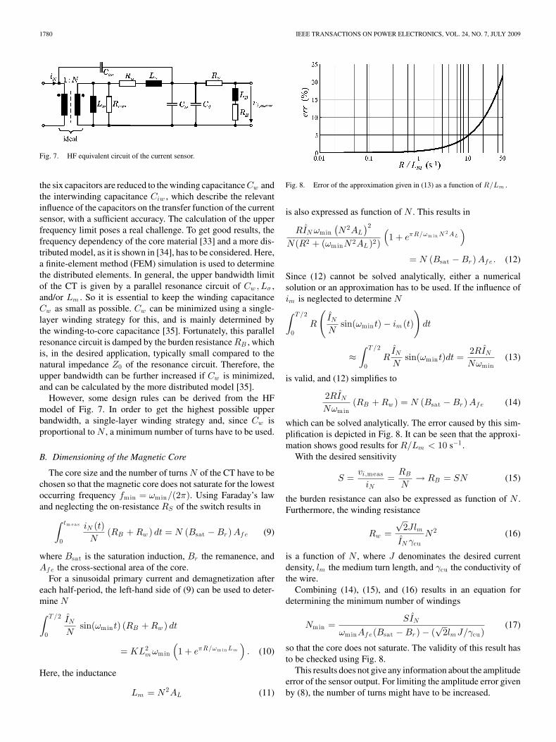
the six capacitors are reduced to the winding capacitance Cw andthe interwinding capacitance Ciw , which describe the relevantinfluence of the capacitors on the transfer function of the currentsensor, with a sufficient accuracy. The calculation of the upperfrequency limit poses a real challenge. To get good results, thefrequency dependency of the core material [33] and a more dis-tributed model, as it is shown in [34], has to be considered. Here,a finite-element method (FEM) simulation is used to determinethe distributed elements. In general, the upper bandwidth limitof the CT is given by a parallel resonance circuit of Cw ,Lσ ,and/or Lm . So it is essential to keep the winding capacitanceCw as small as possible. Cw can be minimized using a single-layer winding strategy for this, and is mainly determined bythe winding-to-core capacitance [35]. Fortunately, this parallelresonance circuit is damped by the burden resistance RB , whichis, in the desired application, typically small compared to thenatural impedance Z0 of the resonance circuit. Therefore, theupper bandwidth can be further increased if Cw is minimized,and can be calculated by the more distributed model [35].
However, some design rules can be derived from the HFmodel of Fig. 7. In order to get the highest possible upperbandwidth, a single-layer winding strategy and, since Cw isproportional to N , a minimum number of turns have to be used.
B. Dimensioning of the Magnetic Core
The core size and the number of turns N of the CT have to bechosen so that the magnetic core does not saturate for the lowestoccurring frequency fmin = ωmin/(2π). Using Faraday’s lawand neglecting the on-resistance RS of the switch results in∫ tm e a s
0
iN (t)N
(RB + Rw ) dt = N (Bsat − Br ) Af e (9)
where Bsat is the saturation induction, Br the remanence, andAf e the cross-sectional area of the core.
For a sinusoidal primary current and demagnetization aftereach half-period, the left-hand side of (9) can be used to deter-mine N∫ T /2
0
IN
Nsin(ωmint) (RB + Rw ) dt
= KL2m ωmin
(1 + eπR/ωm in Lm
). (10)
Here, the inductance
Lm = N 2AL (11)
Fig. 8. Error of the approximation given in (13) as a function of R/Lm .
is also expressed as function of N . This results in
RIN ωmin(N 2AL
)2
N(R2 + (ωminN 2AL )2)
(1 + eπR/ωm in N 2 AL
)= N (Bsat − Br ) Af e. (12)
Since (12) cannot be solved analytically, either a numericalsolution or an approximation has to be used. If the influence ofim is neglected to determine N∫ T /2
0R
(IN
Nsin(ωmint) − im (t)
)dt
≈∫ T /2
0R
IN
Nsin(ωmint)dt =
2RIN
Nωmin(13)
is valid, and (12) simplifies to
2RIN
Nωmin(RB + Rw ) = N (Bsat − Br ) Af e (14)
which can be solved analytically. The error caused by this sim-plification is depicted in Fig. 8. It can be seen that the approxi-mation shows good results for R/Lm < 10 s−1 .
With the desired sensitivity
S =vi,meas
iN=
RB
N→ RB = SN (15)
the burden resistance can also be expressed as function of N .Furthermore, the winding resistance
Rw =√
2Jlm
IN γcuN 2 (16)
is a function of N , where J denominates the desired currentdensity, lm the medium turn length, and γcu the conductivity ofthe wire.
Combining (14), (15), and (16) results in an equation fordetermining the minimum number of windings
Nmin =SIN
ωminAf e(Bsat − Br ) − (√
2lm J/γcu)(17)
so that the core does not saturate. The validity of this result hasto be checked using Fig. 8.
This results does not give any information about the amplitudeerror of the sensor output. For limiting the amplitude error givenby (8), the number of turns might have to be increased.
HARTMANN et al.: WIDEBAND CURRENT TRANSDUCER FOR MEASURING AC SIGNALS WITH LIMITED DC OFFSET 1781
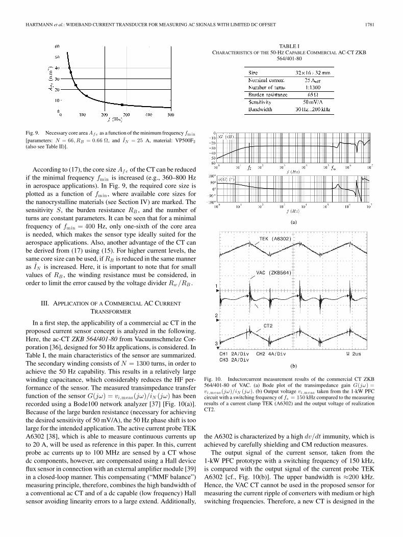
Fig. 9. Necessary core area Af e as a function of the minimum frequency fm in
[parameters: N = 66, RB = 0.66 Ω, and IN = 25 A, material: VP500F2(also see Table II)].
According to (17), the core size Af e of the CT can be reducedif the minimal frequency fmin is increased (e.g., 360–800 Hzin aerospace applications). In Fig. 9, the required core size isplotted as a function of fmin , where available core sizes forthe nanocrystalline materials (see Section IV) are marked. Thesensitivity S, the burden resistance RB , and the number ofturns are constant parameters. It can be seen that for a minimalfrequency of fmin = 400 Hz, only one-sixth of the core areais needed, which makes the sensor type ideally suited for theaerospace applications. Also, another advantage of the CT canbe derived from (17) using (15). For higher current levels, thesame core size can be used, if RB is reduced in the same manneras IN is increased. Here, it is important to note that for smallvalues of RB , the winding resistance must be considered, inorder to limit the error caused by the voltage divider Rw /RB .
III. APPLICATION OF A COMMERCIAL AC CURRENT
TRANSFORMER
In a first step, the applicability of a commercial ac CT in theproposed current sensor concept is analyzed in the following.Here, the ac-CT ZKB 564/401-80 from Vacuumschmelze Cor-poration [36], designed for 50 Hz applications, is considered. InTable I, the main characteristics of the sensor are summarized.The secondary winding consists of N = 1300 turns, in order toachieve the 50 Hz capability. This results in a relatively largewinding capacitance, which considerably reduces the HF per-formance of the sensor. The measured transimpedance transferfunction of the sensor G(jω) = vi,meas(jω)/iN (jω) has beenrecorded using a Bode100 network analyzer [37] [Fig. 10(a)].Because of the large burden resistance (necessary for achievingthe desired sensitivity of 50 mV/A), the 50 Hz phase shift is toolarge for the intended application. The active current probe TEKA6302 [38], which is able to measure continuous currents upto 20 A, will be used as reference in this paper. In this, currentprobe ac currents up to 100 MHz are sensed by a CT whosedc components, however, are compensated using a Hall deviceflux sensor in connection with an external amplifier module [39]in a closed-loop manner. This compensating (“MMF balance”)measuring principle, therefore, combines the high bandwidth ofa conventional ac CT and of a dc capable (low frequency) Hallsensor avoiding linearity errors to a large extend. Additionally,
TABLE ICHARACTERISTICS OF THE 50-HZ CAPABLE COMMERCIAL AC-CT ZKB
564/401-80
Fig. 10. Inductorcurrent measurement results of the commercial CT ZKB564/401-80 of VAC. (a) Bode plot of the transimpedance gain G(jω) =vi,m eas (jω)/iN (jω). (b) Output voltage vi,m eas taken from the 1-kW PFCcircuit with a switching frequency of fs = 150 kHz compared to the measuringresults of a current clamp TEK (A6302) and the output voltage of realizationCT2.
the A6302 is characterized by a high dv/dt immunity, which isachieved by carefully shielding and CM reduction measures.
The output signal of the current sensor, taken from the1-kW PFC prototype with a switching frequency of 150 kHz,is compared with the output signal of the current probe TEKA6302 [cf., Fig. 10(b)]. The upper bandwidth is ≈200 kHz.Hence, the VAC CT cannot be used in the proposed sensor formeasuring the current ripple of converters with medium or highswitching frequencies. Therefore, a new CT is designed in the

1782 IEEE TRANSACTIONS ON POWER ELECTRONICS, VOL. 24, NO. 7, JULY 2009
TABLE IISPECIFICATIONS OF THE MAGNETIC MATERIALS
following section, and the performance of the designed sensoris plotted in Fig. 10(b).
IV. DESIGN OF A HIGH-BANDWIDTH CT
As the commercial CTs are not appropriate for the proposedcurrent sensor (cf., Section III), a CT with the following prop-erties is designed.
1) 50-Hz capability and small amplitude error, as calculatedin (8).
2) High upper cutoff frequency fu .3) Small size of the sensor.4) Good sensitivity S.To achieve a small amplitude error at 50 Hz, the magnetizing
inductance Lm has to be large, which requires either a high-permeability core or a large number of turns N . Unfortunately,both measures reduce the upper bandwidth limit, so a tradeoffhas to be found between the 50-Hz amplitude error and the upperbandwidth limit.
A. Magnetic Materials
For the CT design, the MnZn–ferrite T38 and the twonanocrystalline materials VITROPERM 500F1 (VP500F1) aswell as VITROPERM 500F2 (VP500F2) are compared. Theirproperties are given in Table II. Also, amorphous materials areappropriate for the design of a CT. However, the performanceof the nanocrystalline materials surpasses the amorphous ones,only the nanocrystalline ones are considered in the following.
The two nanocrystalline materials offer the advantage of avery high saturation flux density of Bsat = 1.2 T and showa highly linear B-H characteristic up to Bm,lin = 1 T. Conse-quently, the core size of the CT with nanocrystalline material canbe reduced compared to the MnZn–ferrite material T38 , whichhas just a saturation flux density of Bsat = 0.43 T. The measuredhysteresis loops of the materials are plotted in Fig. 11(a). As de-picted in Fig. 11(b), the initial permeability µr,i is also veryhigh for the nanocrystalline materials. The material VP500F1offers a permeability of µr,i ≈ 100 000 and seems to be best-suited. Unfortunately, this high-permeability material also hasa very high remanence of Br = 0.3 T [cf., Fig. 11(a)], whichreduces the actually applicable amplitude range of the flux den-sity. For the two other materials (with lower µr,i), the influenceof remanence can be neglected. Because of eddy currents, thecomplex permeability decreases for higher frequencies that mustbe considered when determining the sensor’s HF behavior. Thenanocrystalline materials show a very small temperature depen-dence of Bsat and µr . Additionally, the high Curie temperature
Fig. 11. (a) Measured hysteresis loop and (b) complex permeability |µr | as afunction of the frequency f of the magnetic materials.
of more than 600 C allows a higher operating temperature ofthe core, making these materials suitable for power electronicapplications.
B. Current Transformer Design
Using the considered materials, CTs for a sinusoidal pri-mary current of ±25Apk (resulting in a dc component ofiavg = (2/π)I = 15.9 A) and a frequency of 50 Hz have beendesigned, where the CT is assumed to be demagnetized everyhalf-period. The characteristics of the three CTs are summarizedin Table III. As the permeability of the ferrite material usedfor CT3 is much smaller, a bigger core size has to be applied.Equation (17) has been used for determining the minimum num-ber of turns in order to avoid saturation. Since only the coresaturation is considered in (17), the amplitude error of the CT[cf., (8) and the resulting THD (only distortions caused by thedemagnetizing concept are considered) have been calculated fordependency on N (cf., Fig. 13 and Table III).
The amplitude error is reduced by increasing N , which, how-ever, is limited due to the parasitic winding capacitance and theavailable core window. For the given case, it is not possible to

HARTMANN et al.: WIDEBAND CURRENT TRANSDUCER FOR MEASURING AC SIGNALS WITH LIMITED DC OFFSET 1783
Fig. 12. Realized CTs. Sensor CT1 and CT2 use a nanocristalline materialand therefore a smaller core size is possible compared to sensor CT3 with theferrite-material T38 .
TABLE IIICHARACTERISTICS OF THE DESIGNED CURRENT TRANSFORMERS
Fig. 13. Amplitudeerror according to (8) as a function of N . The realizednumber of turns are marked with a small square.
reduce the error below 2% for CT2 and CT3. For a further re-duction of the error, a material with a higher permeability, forexample, VP500F1 , must be used. Sensor CT1 uses the materialwith highest permeability and shows a small amplitude error at50 Hz. Whereas, CT2 is more suited to achieve a high uppercutoff frequency.
In Fig. 14, the measured transimpedance transfer functionsG(jω) of the sensors are plotted. The upper bandwidth limithas to be defined either by the phase error or by the amplitudeerror of the CT. For CT2, both limitations result in an upperfrequency limit of 20 MHz. So, a wideband CT from 50 Hzup to 20 MHz has been realized based on the nanocrystallinematerials. Also, CT3 (using the ferrite material T38 ) shows good,but slightly reduced performance results. For testing the HFbehavior of the sensors, an (damped) oscillating current showinga frequency of about 3 MHz was applied to the primary side.
Fig. 14. Bodeplot of the transimpedance gain G(jω) = vi,m eas (jω)/iN (jω) of the three sensors.
Fig. 15. Currentsensor outputs, measuring a 3 MHz/10 A ringing current.
The results, compared with the measurement of an active TEKA6302 current probe, are given in Fig. 15. Sensor CT2, whichhas the highest bandwidth, exhibits only a negligible deviation,whereas in the signals of CT1 and CT3, the bandwidth limitationbecome visible.
C. dv/dt Immunity Test
In many power electronic applications, a high dv/dt immu-nity is very important in order to limit the noise in the mea-surement signal. With a high dv/dt, the primary side of the CTcouples to the secondary side via the interwinding capacitanceCiw of the sensor (cf., Fig. 7). A high dv/dt is, for example,generated by the switching transient of a MOSFET.
For testing the dv/dt immunity of the sensors, a boost-typeconverter circuit with switching transients of 15 kV/µs has beenused. A stub line was connected to the drain of the MOSFET andwas fed through the CT as primary conductor, where no currentis flowing. Without any shielding, a relatively large noise signalof 2 Apk is coupled to the secondary side [cf., Fig. 16(a)].
The noise can be reduced by shielding the primary inductor[cf., Fig. 16(b)]. Since the secondary winding of the CT is alsocoupled to the surrounded elements, a noticeable disturbanceis still measured as compared to the results of the TEK A6302current probe [cf., Fig. 16(c)]. A further improvement of the

1784 IEEE TRANSACTIONS ON POWER ELECTRONICS, VOL. 24, NO. 7, JULY 2009
Fig. 16. dv/dt immunity test of CT1; voltage slope: 15 kV/µs, CH1: vDS . . . 100 V/Div, time scale: 20 ns/Div. (a) Measurement without shielding:im eas . . . 1 A/Div. (b) Measurement with primary conductor shielded: im eas . . . 1 A/Div. (c) TEK A6302 current probe as reference: im eas . . . 100 mA/Div.
Fig. 17. Possible realizations of the demagnetizing circuit. In (a) two Zenerdiodes are used for demagnetization and (b) two diodes are connected to±VC C ,(c) realization of a bidirectional switch using two MOSFETs, (d) realizationusing just one MOSFET, if the sensor is placed on the dc side of the converter.
dv/dt would require shielding of the entire CT and insertion ofa small common-mode choke at the output of the winding [13].
V. DEMAGNETIZATION CIRCUIT
Several configurations of the demagnetizing circuits are pos-sible in practice, which differ if the sensor is located on the acside or on the dc side of the rectifier. In Fig. 17(a), for example,a demagnetizing circuit using two Zener diodes is shown. Ifa bipolar power supply (e.g., ±12 V) is available, two diodesconnected to the power supply, as shown in Fig. 17(b), can alsobe used. If the sensor is located on the ac side of the converter, abidirectional realization of the switch S2 is required. In the caseof not too high-burden currents, integrated bidirectional analogswitches may be used for realizing S2 . Such analog switchesoffer a typical on-resistance of about 250 mΩ and a currentcapability up to 500 mA. However, for the designed CTs inSection IV, higher burden currents occur. Hence, a bidirectionalswitch arrangement, as shown in Fig. 17(c), is recommended. Ifthe sensor is located on the dc side of the converter, a realization
Fig. 18. Realizedprototype to test the behavior of the proposed current sensorconcept. (a) Picture of the sensor. (b) Schematic of the demagnetizing circuit.(c) PFC prototype (1 kW) where the sensor is located on the dc side of theconverter.
using a single MOSFET is possible [cf., Fig. 17(d)]. For thisrealization also, only a single-clamp diode is necessary.
The realized prototype (cf., Fig. 18) uses the designed sensorCT1, and is based on the proposed bidirectional switch configu-ration of Fig. 17(c). The two MOSFETs are realized by the dualN-channel MOSFET IRF9956. This MOSFET shows a smalloutput capacitance Coss and a sufficient low RDS,on . The gatedrive is realized by a insulated-gate bipolar transistor (IGBT)gate drive optocoupler HCPL0314, which is fast enough andoffers the capability of a bipolar output (see Section VI).
VI. EXPERIMENTAL RESULTS
For determining the performance of the prototype of the cur-rent sensor (cf., Fig. 18) a single-phase 1-kW PFC circuit hasbeen utilized. The sensor prototype designed in Section V islocated on the dc side of the PFC. As already mentioned, theprimary current of the sensor (here, the inductor current iL of
HARTMANN et al.: WIDEBAND CURRENT TRANSDUCER FOR MEASURING AC SIGNALS WITH LIMITED DC OFFSET 1785
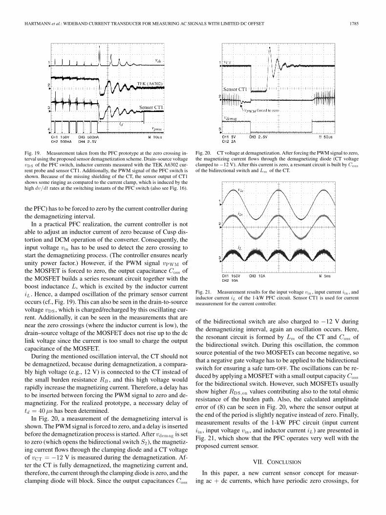
Fig. 19. Measurement taken from the PFC prototype at the zero crossing in-terval using the proposed sensor demagnetization scheme. Drain–source voltagevDS of the PFC switch, inductor currents measured with the TEK A6302 cur-rent probe and sensor CT1. Additionally, the PWM signal of the PFC switch isshown. Because of the missing shielding of the CT, the sensor output of CT1shows some ringing as compared to the current clamp, which is induced by thehigh dv/dt rates at the switching instants of the PFC switch (also see Fig. 16).
the PFC) has to be forced to zero by the current controller duringthe demagnetizing interval.
In a practical PFC realization, the current controller is notable to adjust an inductor current of zero because of Cusp dis-tortion and DCM operation of the converter. Consequently, theinput voltage vin has to be used to detect the zero crossing tostart the demagnetizing process. (The controller ensures nearlyunity power factor.) However, if the PWM signal vPWM ofthe MOSFET is forced to zero, the output capacitance Coss ofthe MOSFET builds a series resonant circuit together with theboost inductance L, which is excited by the inductor currentiL . Hence, a damped oscillation of the primary sensor currentoccurs (cf., Fig. 19). This can also be seen in the drain-to-sourcevoltage vDS , which is charged/recharged by this oscillating cur-rent. Additionally, it can be seen in the measurements that arenear the zero crossings (where the inductor current is low), thedrain–source voltage of the MOSFET does not rise up to the dclink voltage since the current is too small to charge the outputcapacitance of the MOSFET.
During the mentioned oscillation interval, the CT should notbe demagnetized, because during demagnetization, a compara-bly high voltage (e.g., 12 V) is connected to the CT instead ofthe small burden resistance RB , and this high voltage wouldrapidly increase the magnetizing current. Therefore, a delay hasto be inserted between forcing the PWM signal to zero and de-magnetizing. For the realized prototype, a necessary delay oftd = 40µs has been determined.
In Fig. 20, a measurement of the demagnetizing interval isshown. The PWM signal is forced to zero, and a delay is insertedbefore the demagnetization process is started. After vdemag is setto zero (which opens the bidirectional switch S2), the magnetiz-ing current flows through the clamping diode and a CT voltageof vCT = −12 V is measured during the demagnetization. Af-ter the CT is fully demagnetized, the magnetizing current and,therefore, the current through the clamping diode is zero, and theclamping diode will block. Since the output capacitances Coss
Fig. 20. CT voltage at demagnetization. After forcing the PWM signal to zero,the magnetizing current flows through the demagnetizing diode (CT voltageclamped to −12 V). After this current is zero, a resonant circuit is built by Cossof the bidirectional switch and Lm of the CT.
Fig. 21. Measurement results for the input voltage vin , input current iin , andinductor current iL of the 1-kW PFC circuit. Sensor CT1 is used for currentmeasurement for the current controller.
of the bidirectional switch are also charged to −12 V duringthe demagnetizing interval, again an oscillation occurs. Here,the resonant circuit is formed by Lm of the CT and Coss ofthe bidirectional switch. During this oscillation, the commonsource potential of the two MOSFETs can become negative, sothat a negative gate voltage has to be applied to the bidirectionalswitch for ensuring a safe turn-OFF. The oscillations can be re-duced by applying a MOSFET with a small output capacity Cossfor the bidirectional switch. However, such MOSFETs usuallyshow higher RDS,on values contributing also to the total ohmicresistance of the burden path. Also, the calculated amplitudeerror of (8) can be seen in Fig. 20, where the sensor output atthe end of the period is slightly negative instead of zero. Finally,measurement results of the 1-kW PFC circuit (input currentiin , input voltage vin , and inductor current iL ) are presented inFig. 21, which show that the PFC operates very well with theproposed current sensor.
VII. CONCLUSION
In this paper, a new current sensor concept for measur-ing ac + dc currents, which have periodic zero crossings, for

1786 IEEE TRANSACTIONS ON POWER ELECTRONICS, VOL. 24, NO. 7, JULY 2009
example, given in PFC applications, has been analyzed in de-tail. The proposed sensor consists of a CT and an active de-magnetizing circuit, which demagnetizes the core of the CTduring the zero crossings of the current. Here, the measuredcurrent is clamped to zero for a short period of time, whichcoincides with the inherent zero crossing distortions of activePFC circuit, so that the THD of the controlled current is notdeteriorated.
For validating the presented design equations and models,prototype systems utilizing either nanocrystalline or ferrite-core material have been built and the transfer functions havebeen measured. Here, a bandwidth from dc up to 20 MHz andmeasurement errors below 2% have been achieved with thenanocrystalline materials. The bandwidth of the ferrite prototypeis limited to values below 5 MHz, and the resulting measurementerror is relatively high (> 6%). Furthermore, the performanceof the proposed sensor concept has been measured in a 1-kWsingle-phase PFC test system, which revealed a THD of 1.5%.
The design of the proposed sensor is quite simple, and thesize of the CT can be reduced significantly if the frequency ofthe ac current increases, for example, in aircraft power systems.
REFERENCES
[1] J. W. Kolar and F. C. Zach, “A novel three-phase utility interface mini-mizing line current harmonics of high-power telecommunications rectifiermodules,” IEEE Trans. Ind. Electron., vol. 44, no. 4, pp. 456–467, Aug.1997.
[2] T. Nussbaumer, M. Baumann, and J. W. Kolar, “Comprehensive design ofa three-phase three-switch buck-type PWM rectifier,” IEEE Trans. PowerElectron., vol. 22, no. 2, pp. 551–562, Mar. 2007.
[3] K. Sangshin and H. A. Toliyat, “Design and rating comparisons of PWMvoltage source rectifiers and active power filters for AC drives with unitypower factor,” IEEE Trans. Power Electron., vol. 20, no. 5, pp. 1133–1142, Sep. 2005.
[4] F. Blaabjerg, Z. Chen, and S. B. Kjaer, “Power electronics as efficientinterface in dispersed power generation systems,” IEEE Trans. PowerElectron., vol. 19, no. 5, pp. 1184–1194, Sep. 2004.
[5] J. M. Carrasco, L. G. Franquelo, J. T. Bialasiewicz, E. Galvan,R. C. P. Guisado, Ma. A. M. Prats, J. I. Leon, and N. Moreno-Alfonso,“Power-electronic systems for the grid integration of renewable energysources: A survey,” IEEE Trans. Ind. Electron., vol. 53, no. 4, pp. 1002–1016, Jun. 2006.
[6] J. W. Kolar, U. Drofenik, J. Biela, M. L. Heldwein, H. Ertl, T. Friedli, andS. D. Round, “PWM converter power density barriers,” IEEJ, vol. 34,no. 3, pp. 473–479, May/Jun. 1998.
[7] T. Noguchi, H. Tomiki, S. Kondo, and I. Takahashi, “Direct power controlof PWM converter without power-source voltage sensors,” IEEE Trans.Ind. Appl., vol. 34, no. 3, pp. 473–479, May/Jun. 1998.
[8] M. P. Kazmierkowski and L. Malesani, “Current control techniques forthree-phase voltage-source PWM converters: A survey,” IEEE Trans. Ind.Electron., vol. 45, no. 5, pp. 691–703, Oct. 1998.
[9] L. Dalessandro, U. Drofenik, S. D. Round, and J. W. Kolar, “A novelhysteresis current control for three-phase three-level PWM rectifiers,” inProc. 20th Annu. IEEE Appl. Power Electron. Conf. Expo. (APEC 2005),Mar. 6–10, vol. 1, pp. 501–507.
[10] P. Athalye, D. Maksimovic, and R. Erickson, “High-performance frontend converter for avionics applications,” IEEE Trans. Aerosp. Electron.Syst., vol. 39, no. 2, pp. 462–470, Apr. 2003.
[11] A. Radun, “An alternative low-cost current-sensing scheme for high-current power electronics circuits,” IEEE Trans. Ind. Electron., vol. 42,no. 1, pp. 78–84, Feb. 1995.
[12] W. F. Ray and C. R. Hewson, “High performance Rogowski current trans-ducers,” in Proc. Conf. Rec. 35th IEEE Ind. Appl. Conf., 2000, vol. 5,pp. 3083–3090.
[13] F. Costa, E. Laboure, F. Forest, and C. Gautier, “Wide bandwidth, largeAC current probe for power electronics and EMI measurements,” IEEETrans. Ind. Electron., vol. 44, no. 4, pp. 502–511, Aug. 1997.
[14] M. Hartmann, A. Muesing, and J. W. Kolar, “Switching transient shapingof RF power MOSFETs for a 2.5 MHz, three-phase PFC,” in Proc. 7thInt. Conf. Power Electron. (ICPE 2007), Oct. 22–25, pp. 1160–1166.
[15] E. Laboure, F. Costa, and F. Forest, “Current measurement in static con-verters and realization of a high frequency passive current probe (50 A–300 MHz),” in Proc. 5th Eur. Conf. Power Electron. Appl., 1993, Sep.13–16, vol. 4, pp. 478–483.
[16] A. Papp and H. Harms, “Magnetooptical current transformer. 1: Principles,2: Components, 3: Measurements,” Appl. Opt., vol. 19, pp. 3729–3745,1980.
[17] A. P. Friedrich and J. Kunze, Universal Magnetoresistive CurrentSensor for Automotive Applications. Wetzlar-Blankenfeld, Germany:SENSiTEC GmbH, Im Amtmann 6, 6330.
[18] G. Laimer and J. W. Kolar, “Design and experimental analysis of a DC to1 MHz closed loop magnetoresistive current sensor,” in Proc. 20th Annu.IEEE Appl. Power Electron. Conf. Expo. (APEC 2005), Mar. 6–10, vol. 2,pp. 1288–1292.
[19] L. Dalessandro, N. Karrer, and J. W. Kolar, “High-performance planarisolated current sensor for power electronics applications,” IEEE Trans.Power Electron., vol. 22, no. 5, pp. 1682–1692, Sep. 2007.
[20] N. Karrer and P. Hofer-Noser, “A new current measuring principle forpower electronic applications,” in Proc. 11th Int. Symp. Power Semicond.Devices ICs, (ISPSD 1999), pp. 279–282.
[21] L.-L. Lee and C.-L. E. Tasy, “Novel zero ripple DC current transformerdesign,” IEEE Trans. Magn., vol. 35, no. 5, pp. 3514–3516, Sep. 1999.
[22] I. M. Filanovsky and V. A. Piskarev, “Sensing and measurement of DCcurrent using a transformer and RL-multivibrator,” IEEE Trans. CircuitsSyst., vol. 38, no. 11, pp. 1366–1370, Nov. 1991.
[23] L. Ghislanzoni and J. A. Carrasco, “A DC current transformer for largebandwidth and high common-mode rejection,” IEEE Trans. Ind. Electron.,vol. 46, no. 3, pp. 631–636, Jun. 1999.
[24] D. Slomovitz, “Electronic error reduction system for clamp-on probes andmeasuring current transformers,” IEEE Trans. Instrum. Meas., vol. 49,no. 6, pp. 1278–1281, Dec. 2000.
[25] R. W. Erickson and D. Maksimovic, Fundamentals of Power Electronics,2nd ed. New York: Springer-Verlag, 2001, pp. 181–182.
[26] N. McNeill, N. K. Gupta, and W. G. Armstrong, “Active current trans-former circuits for low distortion sensing in switched mode power con-verters,” IEEE Trans. Power Electron., vol. 19, no. 4, pp. 908–917, Jul.2004.
[27] N. McNeill, “Application of reset voltage feedback for droop minimiza-tion in the unidirectional current pulse transformer,” IEEE Trans. PowerElectron., vol. 23, no. 2, pp. 591–599, Mar. 2008.
[28] K.-W. Ma and Y.-S. Lee, “Technique for sensing inductor and DC outputcurrents of PWM DC–DC converter,” IEEE Trans. Power Electron., vol. 9,no. 3, pp. 346–354, May 1994.
[29] J. Sun, “On the zero-crossing distortion in single-phase PFC converters,”IEEE Trans. Power Electron., vol. 19, no. 3, pp. 685–692, May 2004.
[30] Y.-K. Lo, S.-Y. Ou, and H.-J. Chiu, “On evaluating the current distortionof the single-phase switch-mode rectifiers with current slope maps,” IEEETrans. Ind. Electron., vol. 49, no. 5, pp. 1128–1137, Oct. 2002.
[31] J. P. Noon and D. Dalal, “Practical design issues for PFC circuits,” inProc. 12th Annu. IEEE Appl. Power Electron. Conf. Expo. (APEC 1997),Feb. 23–27, vol. 1, pp. 51–58.
[32] J. Biela and J. W. Kolar, “Using transformer parasitics for resonantconverters—A review of the calculation of the stray capacitance of trans-formers,” IEEE Trans. Ind. Appl., vol. 44, no. 1, pp. 223–233, Jan./Feb.2008.
[33] L. Dalessandro, W. G. H. Odendaal, and J. W. Kolar, “HF characterizationand nonlinear modeling of a gapped toroidal magnetic structure,” IEEETrans. Power Electron., vol. 21, no. 5, pp. 1167–1175, Sep. 2006.
[34] P. Poulichet, F. Costa, and E. Laboure, “High-frequency modeling of acurrent transformer by finite-element simulation,” IEEE Trans. Magn.,vol. 39, no. 2, pp. 998–1007, Mar. 2003.
[35] A. Massarini and M. K. Kazimierczuk, “Self-capacitance of inductors,”IEEE Trans. Power Electron., vol. 12, no. 4, Jul. 1997, pp. 671–676.
[36] Vacuumschmelze. (2008). Datasheet of the AC-current sensor ZKB564/401-80 [Online]. Available: www.vacuumschmelze.de
[37] Omicron electronics. (2008). Handbook of the network vector analyzer:Bode100 [Online]. Available: www.omicron-labs.com
[38] Tektronix. (2008). Instructions, A6302 & A6302XL 20 Ampere AC/DCcurrent probes [Online]. Available: www.tektronix.com
[39] Tektronix. (2008). Instructions, AM 503B, AM 5030 & A6300 se-ries 067-0271-00 verification and adjustment kit [Online]. Available:www.tektronix.com
HARTMANN et al.: WIDEBAND CURRENT TRANSDUCER FOR MEASURING AC SIGNALS WITH LIMITED DC OFFSET 1787
Michael Hartmann (S’08) received the B.S. (withhonors) and M.Sc. (with honors) degrees in electri-cal engineering from the University of TechnologyVienna, Vienna, Austria, in 2005 and 2006, re-spectively. He is currently working toward thePh.D. degree at the Power Electronic SystemsLaboratory, Swiss Federal Institute of Technology,Zurich, Switzerland, where he is engaged in ac-tive three phase rectifiers with ultrahigh switchingfrequencies.
He was engaged in switched-mode power ampli-fiers using multicell topologies. His current research interests include activethree-phase rectifiers with ultrahigh switching frequencies.
Juergen Biela (S’04–M’08) received the degree inelectrical engineering and the diploma (with honors)in October 2000 from Friedrich-Alexander Univer-sity (FAU), Erlangen, Germany, and the Ph.D. de-gree from the Power Electronic Systems Laboratory(PES), Eidgenssische Technische Hochschule (ETH)Zurich, Zurich, Switzerland.
He was with Strathclyde University, Scotland,where he was engaged in resonant dc-link invert-ers. He was with the Technical University of Munich,Germany, where he was involved in the active con-
trol of series-connected integrated gate commutated thyristors (IGCTs). He waswith the Research Department, A&D Siemens, Germany, where he was in-volved in inverters with very high switching frequencies, semiconductor (SiC)components, and electromagnetic compatibility (EMC). During 2006, he was aGuest Researcher at the Akagi/Fujita laboratory, Tokyo Institute of Technology,for three months. He is currently a Research Associate at the PES. His currentresearch interests include design, modeling, and optimization of power-factor-corrected PFC/dc–dc converters for future energy systems and the design ofpulse power systems.
Hans Ertl (M’93) received the Dipl.Ing. (M.Sc.) andthe Ph.D. degrees in industrial electronics from theUniversity of Technology Vienna, Vienna, Austria, in1984 and 1991, respectively.
Since 1984, he has been with the University ofTechnology Vienna, where he is currently an As-sociate Professor in the Power Electronics Section,Institute of Electrical Drives and Machines. He hasbeen engaged in numerous industrial and scientificresearch projects in the areas of field-oriented con-trol of ac-drive systems, switch-mode power supplies
for welding and industrial plasma processes, and active rectifier systems. Hehas authored or coauthored numerous scientific papers and patents. His currentresearch interests include switch-mode power amplifiers and multicell topolo-gies, in particular, for the generation of testing signals, for active ripple currentcompensators, and for several applications in the area of renewable energysystems.
Johann W. Kolar (M’89–M’91–SM’04) receivedthe Ph.D. degree (summa cum laude) in indus-trial electronics from the University of TechnologyVienna, Vienna, Austria.
From 1984 to 2001, he was with the Univer-sity of Technology Vienna, where he was engagedin research in close collaboration with the industry.Since Feburary 2001, he has been a Professor andthe Head of the Power Electronics Systems Labo-ratory, Swiss Federal Institute of Technology (ETH)Zurich, Zurich, Switzerland. He has proposed numer-
ous novel converter topologies, e.g., the VIENNA rectifier and the three-phaseac–ac sparse matrix converter concept. He has authored or coauthored morethan 200 scientific papers published in international journals and conferenceproceedings, and has filed more than 50 patents. His current research interestsinclude ultracompact intelligent ac–ac and dc–dc converter modules employinglatest power semiconductor (SiC) technology, novel concepts for cooling andactive electromagnetic interference (EMI) filtering, multidisciplinary simula-tion, bearingless motors, power microelectromechanical system (MEMS), andwireless power transmission.