Enterprise Management: - Where have we been? - Where are we now? - Where are we (or where
Upload
laurence-gilbertCategory
view
214download
0
Where have we been, what have we Where have we been, what have we learned, what questions still learned, what questions still prevail, where are we going?prevail, where are we going?
LinuxExercisesReading
IRAFExercisesReading
CCDsReading
Exercises
Astronomy 480
Review material, make lists, comment, isolate questions that remain, etc. Be prepared to cover as part of whole-class discussion.
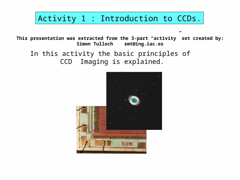
Activity 1 : Introduction to CCDs.
In this activity the basic principles of CCD Imaging is explained.
This presentation was extracted from the 3-part “activity” set created by:Simon Tulloch [email protected]
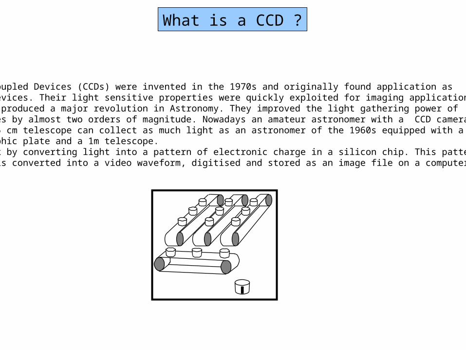
What is a CCD ?
Charge Coupled Devices (CCDs) were invented in the 1970s and originally found application asmemory devices. Their light sensitive properties were quickly exploited for imaging applicationsand they produced a major revolution in Astronomy. They improved the light gathering power of telescopes by almost two orders of magnitude. Nowadays an amateur astronomer with a CCD camera and a 15 cm telescope can collect as much light as an astronomer of the 1960s equipped with a photographic plate and a 1m telescope.CCDs work by converting light into a pattern of electronic charge in a silicon chip. This pattern of charge is converted into a video waveform, digitised and stored as an image file on a computer.

Photoelectric Effect.
The effect is fundamental to the operation of a CCD. Atoms in a silicon crystal have electrons arranged in discrete energy bands. The lower energy band is called the Valence Band, the upper band is the Conduction Band. Most of the electrons occupy the Valence band but can be excited into the conduction band by heatingor by the absorption of a photon. The energy required for this transition is 1.26 electron volts. Once in this conduction band the electron is free to move about in the lattice of the silicon crystal. It leaves behind a ‘hole’ in the valence band which acts like a positively charged carrier. In the absence of an external electric field the hole and electron will quickly re-combine and be lost. In a CCD an electric field is introduced to sweep these charge carriers apart and prevent recombination.
Incr
easi
ng e
nerg
y
Valence Band
Conduction Band
1.26eV
Thermally generated electrons are indistinguishable from photo-generated electrons . They constitute anoise source known as ‘Dark Current’ and it is important that CCDs are kept cold to reduce their number.
1.26eV corresponds to the energy of light with a wavelength of 1m. Beyond this wavelength silicon becomes transparent and CCDs constructed from silicon become insensitive.
photon phot
on
Hole Electron
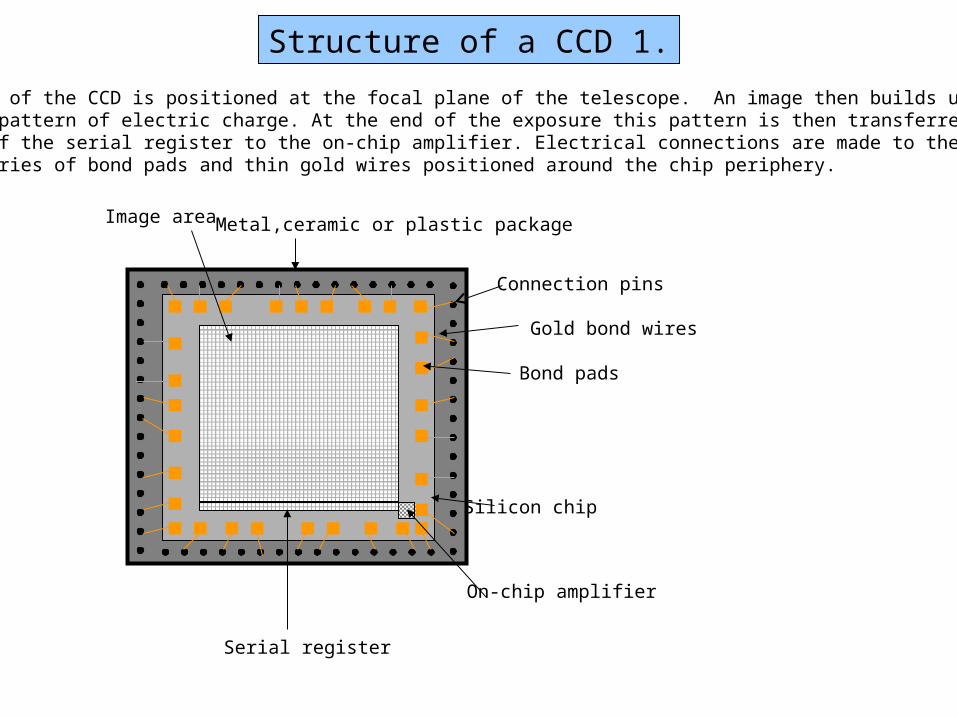
Structure of a CCD 1.
The image area of the CCD is positioned at the focal plane of the telescope. An image then builds up that consists of a pattern of electric charge. At the end of the exposure this pattern is then transferred, pixel at a time, by way of the serial register to the on-chip amplifier. Electrical connections are made to the outside world via a series of bond pads and thin gold wires positioned around the chip periphery.
Connection pins
Gold bond wires
Bond pads
Silicon chip
Metal,ceramic or plastic packageImage area
Serial register
On-chip amplifier
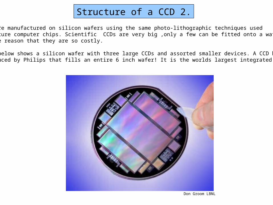
Structure of a CCD 2.
CCDs are are manufactured on silicon wafers using the same photo-lithographic techniques used to manufacture computer chips. Scientific CCDs are very big ,only a few can be fitted onto a wafer. This is one reason that they are so costly.
The photo below shows a silicon wafer with three large CCDs and assorted smaller devices. A CCD has been produced by Philips that fills an entire 6 inch wafer! It is the worlds largest integrated circuit.
Don Groom LBNL

Structure of a CCD 3.
One pixel
Channel stops to define the columns of the image
Transparenthorizontal electrodesto define the pixels vertically. Also used to transfer the charge during readout
Plan View
Cross section
The diagram shows a small section (a few pixels) of the image area of a CCD. This pattern is repeated.
ElectrodeInsulating oxiden-type silicon
p-type silicon
Every third electrode is connected together. Bus wires running down the edge of the chip make the connection. The channel stops are formed from high concentrations of Boron in the silicon.

Structure of a CCD 4.
On-chip amplifierat end of the serial register
Cross section ofserial register
Image Area
Serial Register
Once again every third electrode is in the serial register connected together.
Below the image area (the area containing the horizontal electrodes) is the ‘Serial register’ . This also consists of a group of small surface electrodes. There are three electrodes for every column of the image area

Structure of a CCD 5.
The serial register is bent double to move the output amplifier away from the edgeof the chip. This useful if the CCD is to be used as part of a mosaic.The arrows indicate how charge is transferred through the device.
Edg
e of
Sil
icon
160m
Image Area
Serial Register
Read Out Amplifier
Bu
s w
ires
Photomicrograph of a corner of an EEV CCD.

Structure of a CCD 6.
OD
OS
RDRSW
Output Node
Substrate
Output Transistor
Reset Transistor
SummingWell
20mOutput Drain (OD)
Output Source (OS)
Gate of Output Transistor
Output Node
R
Reset Drain (RD)
Summing Well (SW)
Last few electrodes in Serial Register
Serial Register Electrodes
Photomicrograph of the on-chip amplifier of a Tektronix CCD and its circuit diagram.
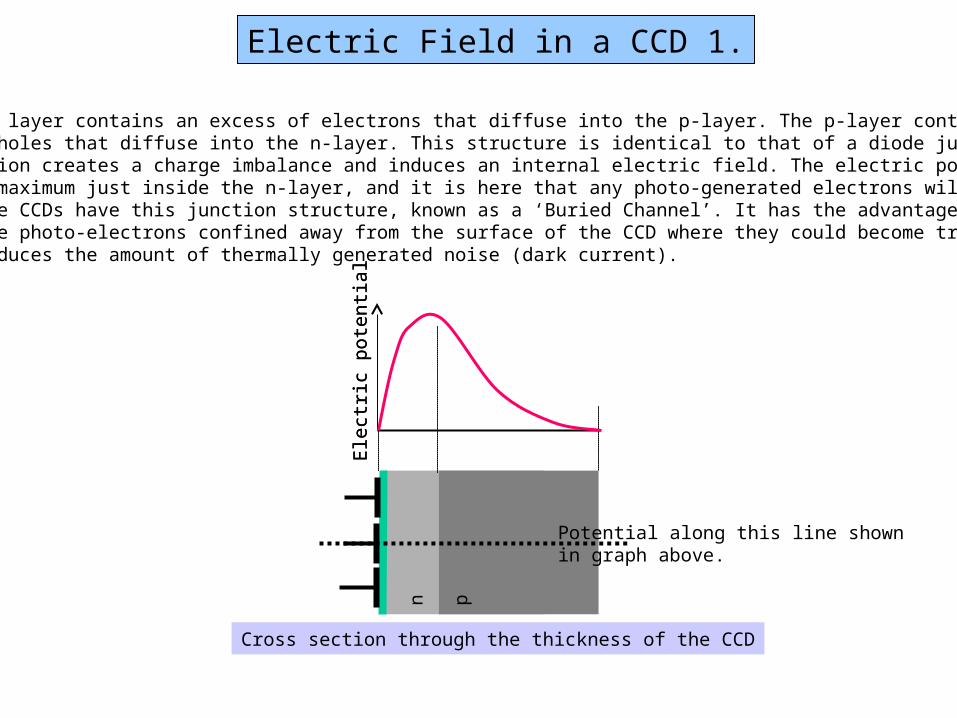
Electric Field in a CCD 1.
The n-type layer contains an excess of electrons that diffuse into the p-layer. The p-layer contains an excess of holes that diffuse into the n-layer. This structure is identical to that of a diode junction. The diffusion creates a charge imbalance and induces an internal electric field. The electric potential reaches a maximum just inside the n-layer, and it is here that any photo-generated electrons will collect. All science CCDs have this junction structure, known as a ‘Buried Channel’. It has the advantage of keeping the photo-electrons confined away from the surface of the CCD where they could become trapped. It also reduces the amount of thermally generated noise (dark current).
n p
Ele
ctri
c po
tent
ial
Potential along this line shownin graph above.
Ele
ctri
c po
tent
ial
Cross section through the thickness of the CCD
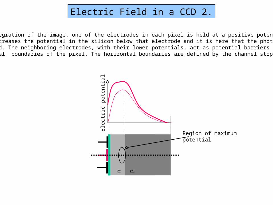
Electric Field in a CCD 2.
During integration of the image, one of the electrodes in each pixel is held at a positive potential. This further increases the potential in the silicon below that electrode and it is here that the photoelectrons are accumulated. The neighboring electrodes, with their lower potentials, act as potential barriers that definethe vertical boundaries of the pixel. The horizontal boundaries are defined by the channel stops.
n p
Ele
ctri
c po
tent
ial
Region of maximum potential
pixe
l bo
unda
ry
Charge packetp-type silicon
n-type silicon
SiO2 Insulating layer
Electrode Structure
pixe
l bo
unda
ry
inco
min
gph
oton
s
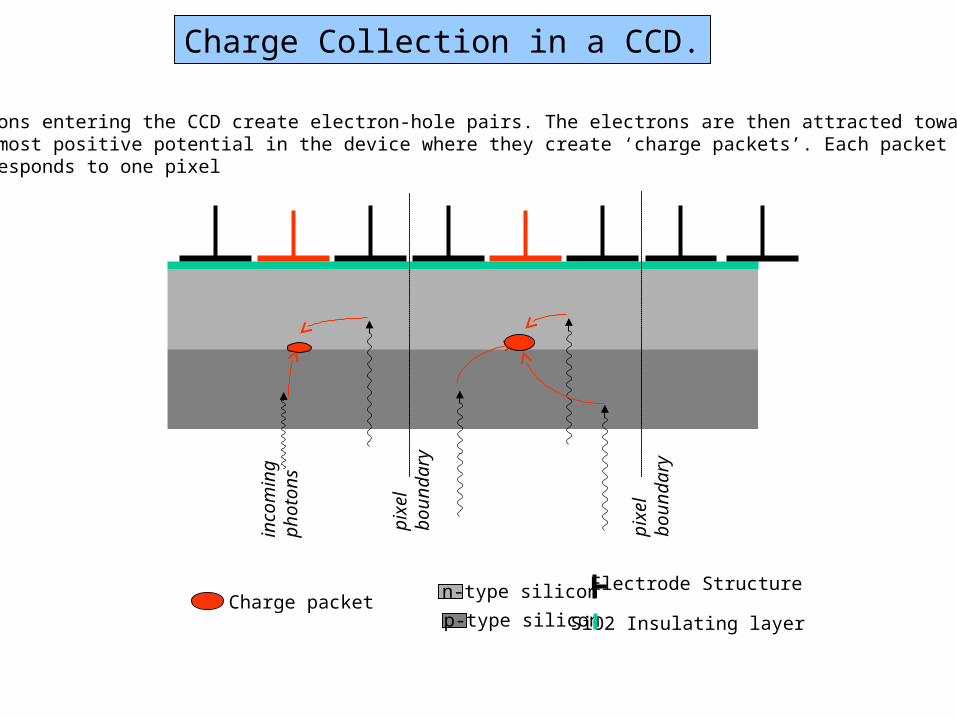
Charge Collection in a CCD.
Photons entering the CCD create electron-hole pairs. The electrons are then attracted towards the most positive potential in the device where they create ‘charge packets’. Each packet corresponds to one pixel

Charge Transfer in a CCD 1.
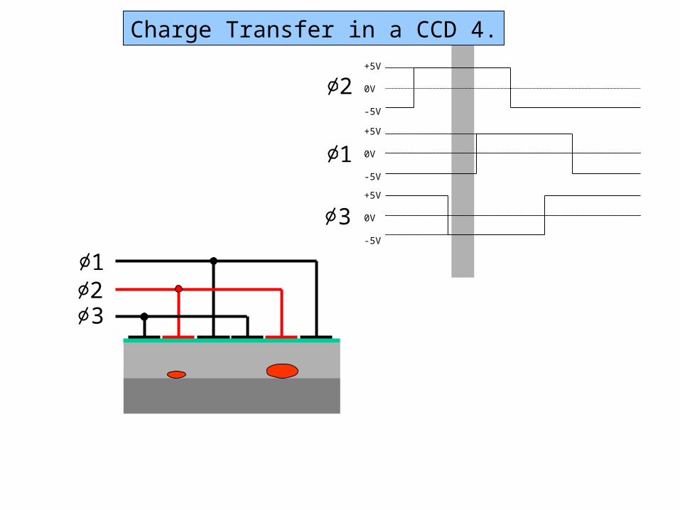
In the following few slides, the implementation of the ‘conveyor belts’ as actual electronicstructures is explained.
The charge is moved along these conveyor belts by modulating the voltages on the electrodespositioned on the surface of the CCD. In the following illustrations, electrodes colour coded redare held at a positive potential, those coloured black are held at a negative potential.
123

123
+5V
0V
-5V
+5V
0V
-5V
+5V
0V
-5V
Time-slice shown in diagram
1
2
3
Charge Transfer in a CCD 2.

123
+5V
0V
-5V
+5V
0V
-5V
+5V
0V
-5V
1
2
3
Charge Transfer in a CCD 3.
123
+5V
0V
-5V
+5V
0V
-5V
+5V
0V
-5V
1
2
3
Charge Transfer in a CCD 4.

123
+5V
0V
-5V
+5V
0V
-5V
+5V
0V
-5V
1
2
3
Charge Transfer in a CCD 5.

123
+5V
0V
-5V
+5V
0V
-5V
+5V
0V
-5V
1
2
3
Charge Transfer in a CCD 6.
123
+5V
0V
-5V
+5V
0V
-5V
+5V
0V
-5V
1
2
3
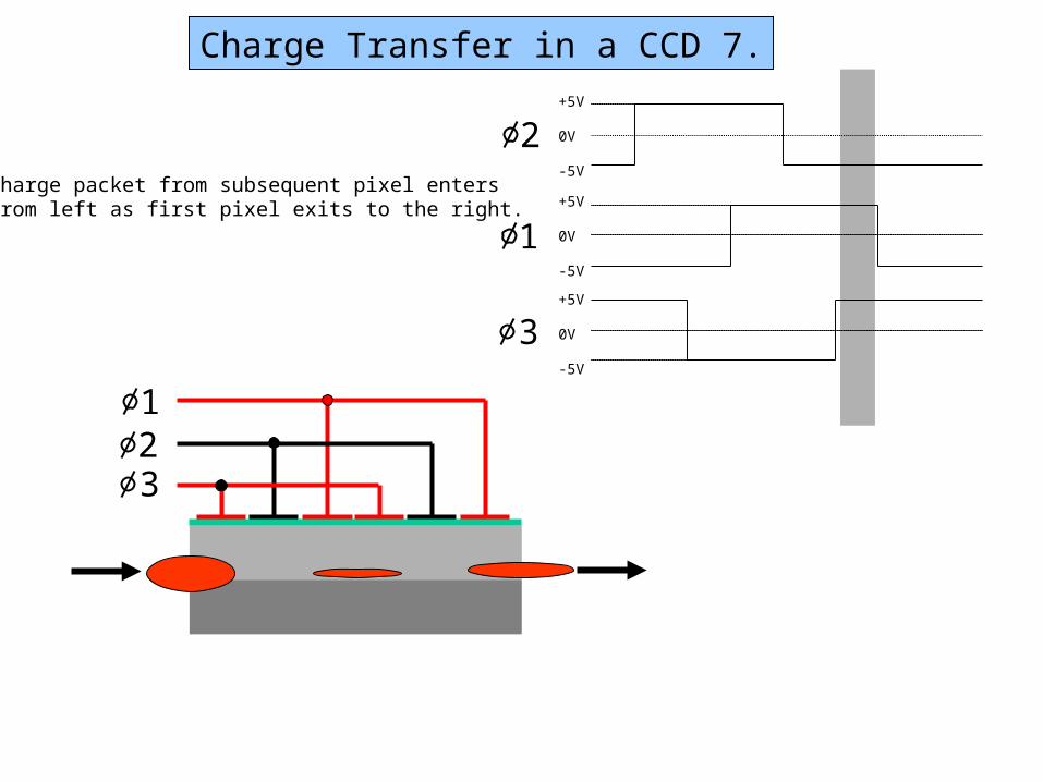
Charge Transfer in a CCD 7.
Charge packet from subsequent pixel entersfrom left as first pixel exits to the right.
123
+5V
0V
-5V
+5V
0V
-5V
+5V
0V
-5V
1
2
3
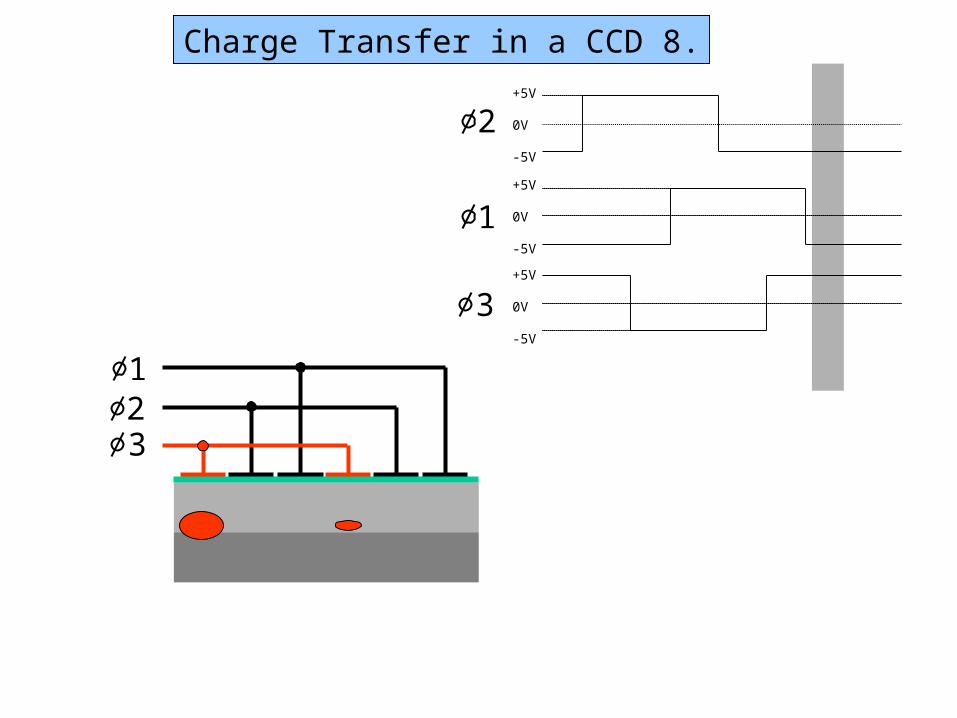
Charge Transfer in a CCD 8.
On-Chip Amplifier 1.
OD
OS
RDRSW
Output Node Output
Transistor
Reset Transistor
SummingWell
+5V
0V
-5V
+10V
0V
R
SW
--end of serial register
Vout
Vout
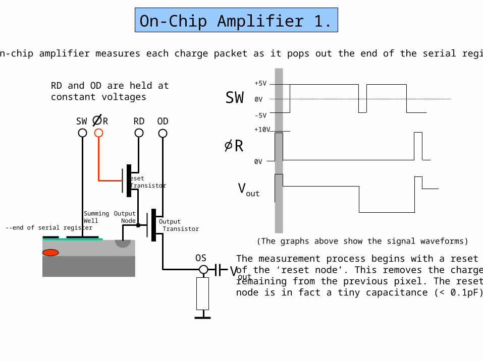
The on-chip amplifier measures each charge packet as it pops out the end of the serial register.
The measurement process begins with a resetof the ‘reset node’. This removes the charge remaining from the previous pixel. The resetnode is in fact a tiny capacitance (< 0.1pF)
RD and OD are held at constant voltages
(The graphs above show the signal waveforms)
On-Chip Amplifier 2.
OD
OS
RDRSW
Output Node Output
Transistor
Reset Transistor
SummingWell
+5V
0V
-5V
+10V
0V
R
SW
--end of serial register
Vout
Vout
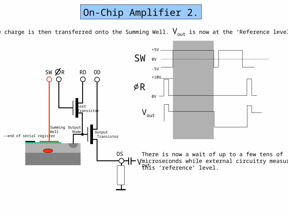
The charge is then transferred onto the Summing Well. Vout is now at the ‘Reference level’
There is now a wait of up to a few tens of microseconds while external circuitry measuresthis ‘reference’ level.
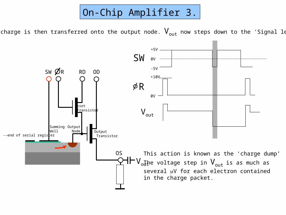
On-Chip Amplifier 3.
OD
OS
RDRSW
Output Node Output
Transistor
Reset Transistor
SummingWell
+5V
0V
-5V
+10V
0V
R
SW
--end of serial register
Vout
Vout
This action is known as the ‘charge dump’
The voltage step in Vout is as much as
several V for each electron contained in the charge packet.
The charge is then transferred onto the output node. Vout now steps down to the ‘Signal level’

On-Chip Amplifier 4.
OD
OS
RDRSW
Output Node Output
Transistor
Reset Transistor
SummingWell
+5V
0V
-5V
+10V
0V
R
SW
--end of serial register
Vout
Vout
Vout is now sampled by external circuitry for up to a few tens of microseconds.
The sample level - reference level will be proportional to the size of the input charge packet.

Spectral Sensitivity of CCDs
The graph below shows the transmission of the atmosphere when looking at objects at the zenith. The atmosphere absorbs strongly below about 330nm, in the near ultraviolet part of the spectrum. An ideal CCD should have a good sensitivity from 330nm to approximately 1000nm, at which point silicon, from which CCDs are manufactured, becomes transparent and therefore insensitive.
Wavelength (Nanometers)
Tra
nsm
issi
on o
f A
tmos
pher
e
Over the last 25 years of development, the sensitivity of CCDs has improved enormously, to the point where almost all of the incident photons across the visible spectrum are detected. CCD sensitivity has been improved using two main techniques : ‘thinning’ and the use of anti-reflection coatings. These are now explained in more detail.

Thick Front-side Illuminated CCD
These are cheap to produce using conventional wafer fabrication techniques. They are used in consumer imaging applications. Even though not all the photons are detected, these devices are still more sensitive than photographic film.
They have a low Quantum Efficiency due to the reflection and absorption of light in the surface electrodes. Very poor blue response. The electrode structure prevents the use of an Anti-reflective coating that would otherwise boost performance.
The amateur astronomer on a limited budget might consider using thick CCDs. For professional observatories, the economies of running a large facility demand that the detectorsbe as sensitive as possible; thick front-side illuminated chips are seldom if ever used.
n-type silicon
p-type silicon
Silicon dioxide insulating layerPolysilicon electrodes
Inco
min
g ph
oton
s
625m

Anti-Reflection Coatings 1
n of air or vacuum is 1.0, glass is 1.46, water is 1.33, Silicon is 3.6. Using the above equation we can show that window glass in air reflects 3.5% and silicon in air reflects 32%. Unless we take steps to eliminate this reflected portion, then a silicon CCD will at best only detect 2 out of every 3 photons.
The solution is to deposit a thin layer of a transparent dielectric material on the surface of the CCD. The refractive index of this material should be between that of silicon and air, and it should have an optical thickness = 1/4 wavelength of light. The question now is what wavelength should we choose, since we are interested in a wide range of colours. Typically 550nm is chosen, which is close to the middle of the optical spectrum.
Silicon has a very high Refractive Index (denoted by n). This means that photons are strongly reflected from its surface.
nt-ni
nt+ni
ni
nt
Fraction of photons reflected at the interface between two mediums of differing refractive indices
= [ ]2
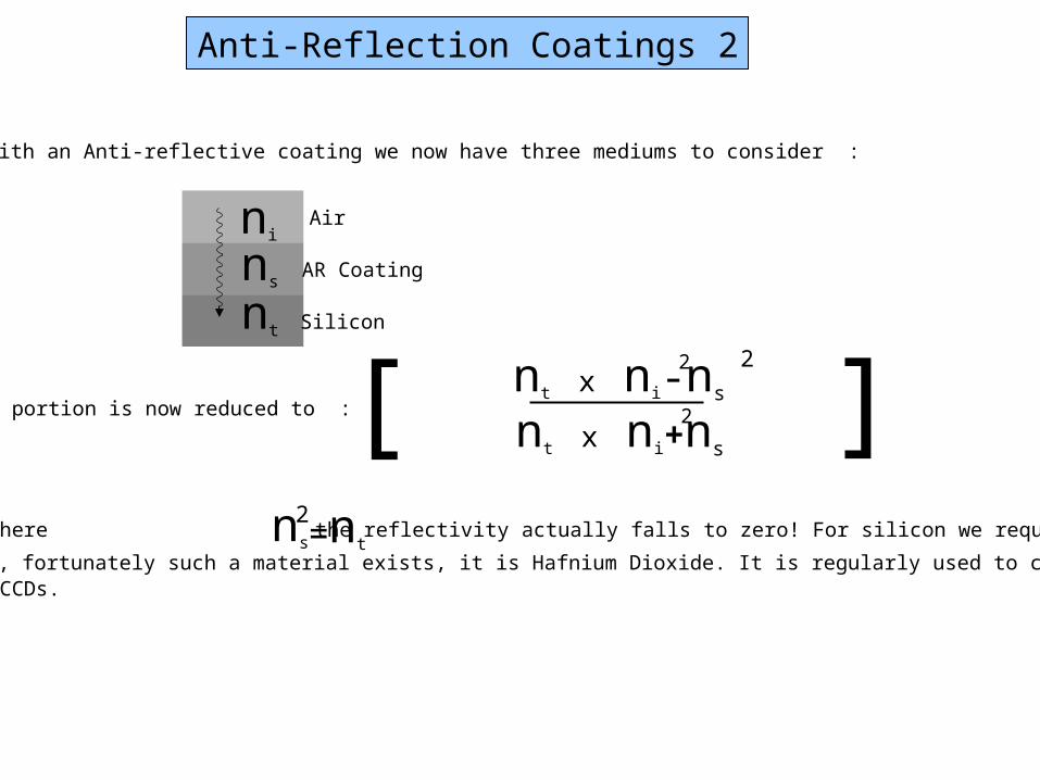
Anti-Reflection Coatings 2
The reflected portion is now reduced to :
In the case where the reflectivity actually falls to zero! For silicon we require a material
with n = 1.9, fortunately such a material exists, it is Hafnium Dioxide. It is regularly used to coat astronomical CCDs.
With an Anti-reflective coating we now have three mediums to consider :
nt
Airni
nsAR Coating
Silicon
[ ]nt x ni-ns
2
nt x ni+ns
2
2
ns nt
2=

Thinned Back-side Illuminated CCD
The silicon is chemically etched and polished down to a thickness of about 15microns. Light enters from the rear and so the electrodes do not obstruct the photons. The QE can approach 100% .
These are very expensive to produce since the thinning is a non-standard process that reduces the chip yield. These thinned CCDs become transparent to near infra-red light and the red response is poor. Response can be boosted by the application of an anti-reflective coating on the thinned rear-side. These coatings do not work so well for thick CCDs due to the surface bumps created by the surface electrodes.
Almost all Astronomical CCDs are Thinned and Backside Illuminated.
n-type silicon
p-type silicon
Silicon dioxide insulating layerPolysilicon electrodes
Inco
min
g ph
oton
s
Anti-reflective (AR) coating
15m
Ele
ctri
c po
tent
ial
Ele
ctri
c po
tent
ial
Cross section through a thinned CCD
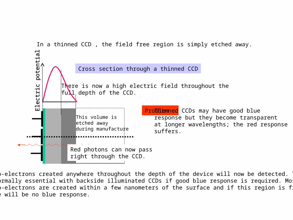
In a thinned CCD , the field free region is simply etched away.
There is now a high electric field throughout the full depth of the CCD.
Photo-electrons created anywhere throughout the depth of the device will now be detected. Thinning is normally essential with backside illuminated CCDs if good blue response is required. Most blue photo-electrons are created within a few nanometers of the surface and if this region is field free,there will be no blue response.
This volume is etched away during manufacture
Problem : Thinned CCDs may have good blue response but they become transparent at longer wavelengths; the red responsesuffers.
Red photons can now passright through the CCD.
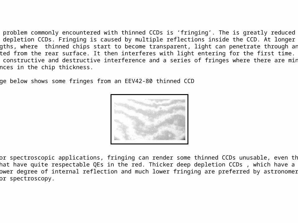
Another problem commonly encountered with thinned CCDs is ‘fringing’. The is greatly reduced in deep depletion CCDs. Fringing is caused by multiple reflections inside the CCD. At longer wavelengths, where thinned chips start to become transparent, light can penetrate through and be reflected from the rear surface. It then interferes with light entering for the first time. This can give rise to constructive and destructive interference and a series of fringes where there are minor differences in the chip thickness.
The image below shows some fringes from an EEV42-80 thinned CCD
For spectroscopic applications, fringing can render some thinned CCDs unusable, even thosethat have quite respectable QEs in the red. Thicker deep depletion CCDs , which have a muchlower degree of internal reflection and much lower fringing are preferred by astronomersfor spectroscopy.
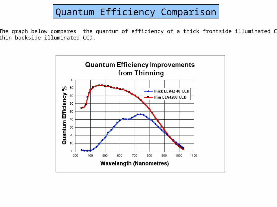
Quantum Efficiency Comparison
The graph below compares the quantum of efficiency of a thick frontside illuminated CCD and a thin backside illuminated CCD.

‘Internal’ Quantum Efficiency
If we take into account the reflectivity losses at the surface of a CCD we can produce a graph showingthe ‘internal QE’ : the fraction of the photons that enter the CCDs bulk that actually produce a detected photo-electron. This fraction is remarkably high for a thinned CCD. For the EEV 42-80 CCD,shown below, it is greater than 85% across the full visible spectrum. Todays CCDs are very close to being ideal visible light detectors!
pixe
l bo
unda
ry
Pho
tons
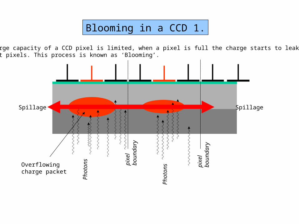
Blooming in a CCD 1.
The charge capacity of a CCD pixel is limited, when a pixel is full the charge starts to leak intoadjacent pixels. This process is known as ‘Blooming’.
Pho
tons
Overflowingcharge packet
Spillage Spillage
pixe
l bo
unda
ry
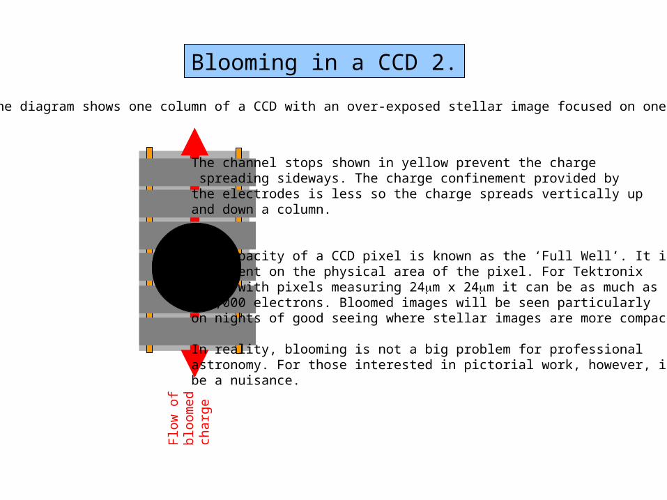
Blooming in a CCD 2.
The diagram shows one column of a CCD with an over-exposed stellar image focused on one pixel.
The channel stops shown in yellow prevent the charge spreading sideways. The charge confinement provided bythe electrodes is less so the charge spreads vertically upand down a column.
The capacity of a CCD pixel is known as the ‘Full Well’. It isdependent on the physical area of the pixel. For TektronixCCDs, with pixels measuring 24m x 24m it can be as much as300,000 electrons. Bloomed images will be seen particularly on nights of good seeing where stellar images are more compact .
In reality, blooming is not a big problem for professionalastronomy. For those interested in pictorial work, however, it canbe a nuisance.
Flo
w o
f bl
oom
ed
char
ge

Blooming in a CCD 3.
Bloomed star images
The image below shows an extended source with bright embedded stars. Due to the longexposure required to bring out the nebulosity, the stellar images are highly overexposedand create bloomed images.
(The image is from a CCD mosaic and the black strip down the center is the space between adjacent detectors)
M42

Image Defects in a CCD 1.Unless one pays a huge amount it is generally difficult to obtain a CCD free of image defects. The first kind of defect is a ‘dark column’. Their locations are identified from flat field exposures.
Flat field exposure of an EEV42-80 CCD
Dark columns are caused by ‘traps’ that block the vertical transfer of charge during image readout. The CCD shown at left has at least 7 dark columns, some grouped together inadjacent clusters.
Traps can be caused by crystal boundaries in the silicon of the CCD or by manufacturing defects.
Although they spoil the chip cosmetically, dark columns are not a big problem for astronomers. This chip has 2048 image columns so 7 bad columns represents a tiny loss of data.
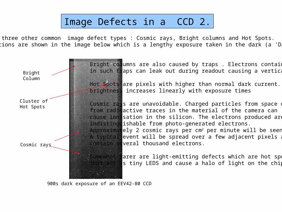
Image Defects in a CCD 2.
Bright columns are also caused by traps . Electrons containedin such traps can leak out during readout causing a vertical streak.
Hot Spots are pixels with higher than normal dark current. Theirbrightness increases linearly with exposure times
Cosmic rays are unavoidable. Charged particles from space orfrom radioactive traces in the material of the camera cancause ionisation in the silicon. The electrons produced areindistinguishable from photo-generated electrons. Approximately 2 cosmic rays per cm2 per minute will be seen.A typical event will be spread over a few adjacent pixels and contain several thousand electrons.
Somewhat rarer are light-emitting defects which are hot spots that act as tiny LEDS and cause a halo of light on the chip.
There are three other common image defect types : Cosmic rays, Bright columns and Hot Spots.Their locations are shown in the image below which is a lengthy exposure taken in the dark (a ‘Dark Frame’)
Cosmic rays
Cluster ofHot Spots
BrightColumn
900s dark exposure of an EEV42-80 CCD

Image Defects in a CCD 3.
M51
Some defects can arise from the processing electronics. This negative image has a bright line in the first image row.
Dark column
Hot spots and bright columns
Bright first image row caused byincorrect operation of signalprocessing electronics.
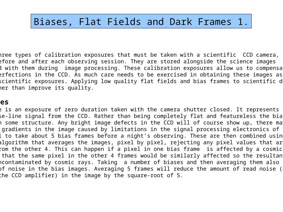
Biases, Flat Fields and Dark Frames 1.
These are three types of calibration exposures that must be taken with a scientific CCD camera, generally before and after each observing session. They are stored alongside the science imagesand combined with them during image processing. These calibration exposures allow us to compensate forcertain imperfections in the CCD. As much care needs to be exercised in obtaining these images as forthe actual scientific exposures. Applying low quality flat fields and bias frames to scientific data can degrade rather than improve its quality.
Bias FramesA bias frame is an exposure of zero duration taken with the camera shutter closed. It represents the zero point or base-line signal from the CCD. Rather than being completely flat and featureless the bias frame may contain some structure. Any bright image defects in the CCD will of course show up, there may be also slight gradients in the image caused by limitations in the signal processing electronics of the camera. It is normal to take about 5 bias frames before a night’s observing. These are then combined using an image processing algorithm that averages the images, pixel by pixel, rejecting any pixel values that are appreciably different from the other 4. This can happen if a pixel in one bias frame is affected by a cosmic ray event. It is unlikely that the same pixel in the other 4 frames would be similarly affected so the resultant ‘master bias’,should be uncontaminated by cosmic rays. Taking a number of biases and then averaging them also reducesthe amount of noise in the bias images. Averaging 5 frames will reduce the amount of read noise (electronic noise from the CCD amplifier) in the image by the square-root of 5.

Biases, Flat Fields and Dark Frames 2.
Flat FieldsSome pixels in a CCD will be more sensitive than others. In addition there may be dust spots on the surfaceof either the chip, the window of the camera or the coloured filters mounted in front of the camera. A star focused onto one part of a chip may therefore produce a lower signal than it might do elsewhere. These variations in sensitivity across the surface of the CCD must be calibrated out or they will add noise to the image. The way to do this is to take a ‘flat-field ‘ image : an image in which the CCD is evenly illuminated with light. Dividing the science image , pixel by pixel , by a flat field image will remove these sensitivityvariations very effectively. Since some of these variations are caused by shadowing from dust spots, it is important that the flat fields are taken shortly before or after the science exposures; the dust may move around! As with biases, it is normal to take several flat field frames and average them to produce a ‘Master’.A flat field is taken by pointing the telescope at an extended , evenly illuminated source. The twilight sky orthe inside of the telescope dome are the usual choices. An exposure time is chosen that gives pixel values about halfway to their saturation level i.e. a medium level exposure.
Dark Frames.Dark current is generally absent from professional cameras since they are operated cold using liquid nitrogen as a coolant. Amateur systems running at higher temperatures will have some dark current and its effect must be minimised by obtaining ‘dark frames’ at the beginning of the observing run. These are exposureswith the same duration as the science frames but taken with the camera shutter closed. These are later subtractedfrom the science frames. Again, it is normal to take several dark frames and combine them to form a Master,using a technique that rejects cosmic ray features.

Dark Frame Flat Field
A dark frame and a flat field from the same EEV42-80 CCD are shown below. The dark frame shows a number of bright defects on the chip. The flat field shows a criss-cross patterning on the chip created during manufacture and a slight loss of sensitivity in two corners of the image. Some dustspots are also visible.
Biases, Flat Fields and Dark Frames 3.

Flat Field Image
Bias Image
Flat-Bias
Science -Dark
Output Image
Flat-Bias
Science -Dark
Dark Frame
Science Frame
Biases, Flat Fields and Dark Frames 4.
If there is significant dark current present, the various calibration and science framesare combined by the following series of subtractions and divisions :
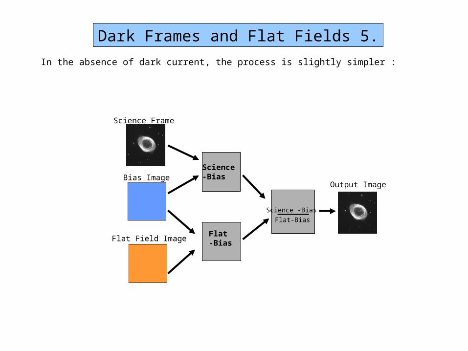
Dark Frames and Flat Fields 5.
Flat Field Image
Bias Image
Flat-Bias
Science -Bias
Output Image
Flat-Bias
Science -Bias
Science Frame
In the absence of dark current, the process is slightly simpler :

Noise Sources in a CCD Image 1.
The main noise sources found in a CCD are :
1. READ NOISE. Caused by electronic noise in the CCD output transistor and possibly also in the external circuitry.Read noise places a fundamental limit on the performance of a CCD. It can be reduced at the expense of increased read out time. Scientific CCDs have a readout noise of 2-3 electrons RMS.
2. DARK CURRENT.Caused by thermally generated electrons in the CCD. Eliminated by cooling the CCD.
3. PHOTON NOISE. Also called ‘Shot Noise’. It is due to the fact that the CCD detects photons. Photons arrive in anunpredictable fashion described by Poissonian statistics. This unpredictability causes noise.
4. PIXEL RESPONSE NON-UNIFORMITY.Defects in the silicon and small manufacturing defects can cause some pixels to have a higher sensitivity than their neighbours. This noise source can be removed by ‘Flat Fielding’; an image processing technique.

Noise Sources in a CCD Image 2.
Before these noise sources are explained further some new terms need to be introduced.
FLAT FIELDINGThis involves exposing the CCD to a very uniform light source that produces a featureless and evenexposure across the full area of the chip. A flat field image can be obtained by exposing on a twilight sky or on an illuminated white surface held close to the telescope aperture (for example the inside of the dome). Flat field exposures are essential for the reduction of astronomical data.
BIAS REGIONSA bias region is an area of a CCD that is not sensitive to light. The value of pixels in a bias region is determined by the signal processing electronics. It constitutes the zero-signal level of the CCD.The bias region pixels are subject only to readout noise. Bias regions can be produced by ‘over-scanning’ a CCD, i.e. reading out more pixels than are actually present. Designing a CCD witha serial register longer than the width of the image area will also create vertical bias strips at the leftand right sides of the image. These strips are known as the ‘x-underscan’ and ‘x-overscan’ regions
A flat field image containing bias regions can yield valuable information not only on the variousnoise sources present in the CCD but also about the gain of the signal processing electronicsi.e. the number of photoelectrons represented by each digital unit (ADU) output by the camera’sAnalogue to Digital Converter.

Noise Sources in a CCD Image 3.
Flat field images obtained from two CCD geometries are represented below. The arrows representthe position of the readout amplifier and the thick black line at the bottom of each image represents the serial register.
CCD With SerialRegister equal inlength to the image area width.
CCD With SerialRegister greater inlength than the image area width.
Image Area
Image Area
X-o
vers
can
X-o
vers
can
X-u
nder
scan
Y-overscan
Y-overscan
Here, the CCD is over-scanned in X and Y
Here, the CCD is over-scanned in Yto produce the Y-overscan bias area.The X-underscan and X-overscan are created by extensions to the serial register on either side of the image area. When charge is transferred from the image area into the serial register, these extensionsdo not receive any photo-charge.
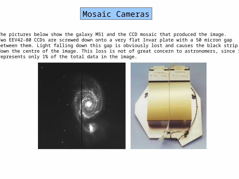
Mosaic Cameras
The pictures below show the galaxy M51 and the CCD mosaic that produced the image.Two EEV42-80 CCDs are screwed down onto a very flat Invar plate with a 50 micron gapbetween them. Light falling down this gap is obviously lost and causes the black stripdown the centre of the image. This loss is not of great concern to astronomers, since it represents only 1% of the total data in the image.

Mosaic Cameras
The Horsehead Nebula in Orion. The mosaic mounted in its camera.

Picture : Canada France Hawaii Telescope
Mosaic Cameras
This colossal mosaic of 12 CCDs is in operation at the CFHT in Hawaii. Here is an example of what it can produce. The chips are of fairly low cosmetic quality.

Mosaic Cameras
This mosaic of 4 science CCDs was built at the Royal Greenwich Observatory. The positioningof the CCDs is somewhat unusual but ultimately all that matters is the total area covered . A smaller fifth CCD on the right hand side is used for auto-guiding the telescope. An example of this camera’s output is shown on the left.
M13

QuickTime™ and aTIFF (Uncompressed) decompressor
are needed to see this picture.