What to Lock? Functional and Parametric Locking
6
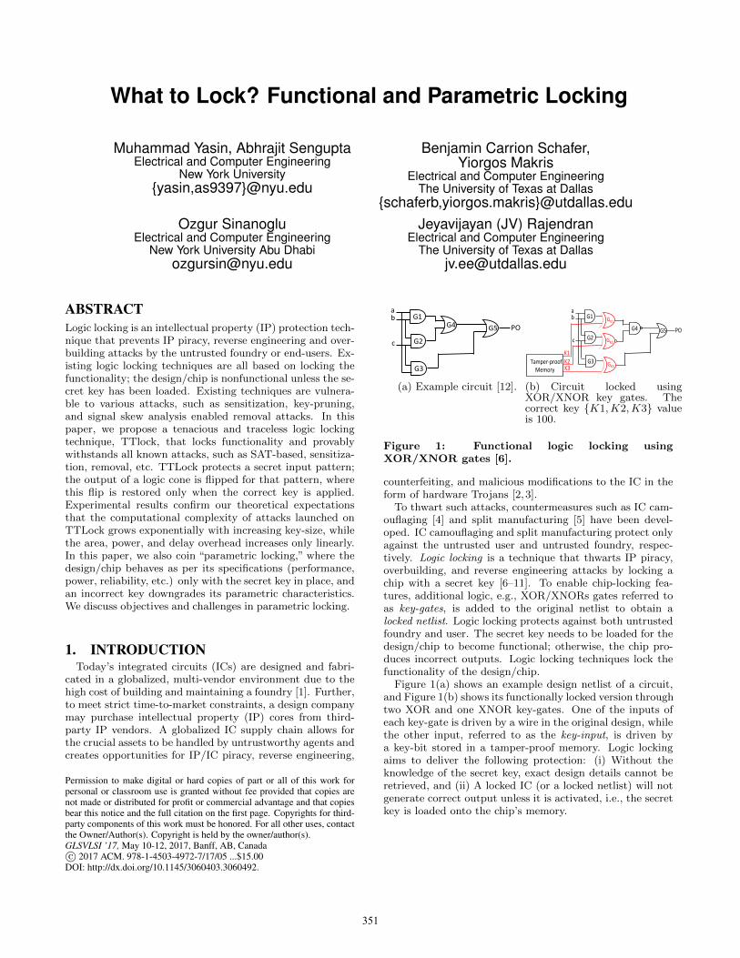
What to Lock? Functional and Parametric Locking Muhammad Yasin, Abhrajit Sengupta Electrical and Computer Engineering New York University {yasin,as9397}@nyu.edu Benjamin Carrion Schafer, Yiorgos Makris Electrical and Computer Engineering The University of Texas at Dallas {schaferb,yiorgos.makris}@utdallas.edu Ozgur Sinanoglu Electrical and Computer Engineering New York University Abu Dhabi [email protected] Jeyavijayan (JV) Rajendran Electrical and Computer Engineering The University of Texas at Dallas [email protected] ABSTRACT Logic locking is an intellectual property (IP) protection tech- nique that prevents IP piracy, reverse engineering and over- building attacks by the untrusted foundry or end-users. Ex- isting logic locking techniques are all based on locking the functionality; the design/chip is nonfunctional unless the se- cret key has been loaded. Existing techniques are vulnera- ble to various attacks, such as sensitization, key-pruning, and signal skew analysis enabled removal attacks. In this paper, we propose a tenacious and traceless logic locking technique, TTlock, that locks functionality and provably withstands all known attacks, such as SAT-based, sensitiza- tion, removal, etc. TTLock protects a secret input pattern; the output of a logic cone is flipped for that pattern, where this flip is restored only when the correct key is applied. Experimental results confirm our theoretical expectations that the computational complexity of attacks launched on TTLock grows exponentially with increasing key-size, while the area, power, and delay overhead increases only linearly. In this paper, we also coin “parametric locking,” where the design/chip behaves as per its specifications (performance, power, reliability, etc.) only with the secret key in place, and an incorrect key downgrades its parametric characteristics. We discuss objectives and challenges in parametric locking. 1. INTRODUCTION Today’s integrated circuits (ICs) are designed and fabri- cated in a globalized, multi-vendor environment due to the high cost of building and maintaining a foundry [1]. Further, to meet strict time-to-market constraints, a design company may purchase intellectual property (IP) cores from third- party IP vendors. A globalized IC supply chain allows for the crucial assets to be handled by untrustworthy agents and creates opportunities for IP/IC piracy, reverse engineering, Permission to make digital or hard copies of part or all of this work for personal or classroom use is granted without fee provided that copies are not made or distributed for profit or commercial advantage and that copies bear this notice and the full citation on the first page. Copyrights for third- party components of this work must be honored. For all other uses, contact the Owner/Author(s). Copyright is held by the owner/author(s). GLSVLSI ’17, May 10-12, 2017, Banff, AB, Canada c 2017 ACM. 978-1-4503-4972-7/17/05 ...$15.00 DOI: http://dx.doi.org/10.1145/3060403.3060492. G1 G2 G3 G5 a b c PO G4 (a) Example circuit [12]. G1 G2 G3 G5 a b c PO K3 K1 K2 G K1 G K2 G K3 Tamper2proof Memory G4 (b) Circuit locked using XOR/XNOR key gates. The correct key {K1,K2,K3} value is 100. Figure 1: Functional logic locking using XOR/XNOR gates [6]. counterfeiting, and malicious modifications to the IC in the form of hardware Trojans [2,3]. To thwart such attacks, countermeasures such as IC cam- ouflaging [4] and split manufacturing [5] have been devel- oped. IC camouflaging and split manufacturing protect only against the untrusted user and untrusted foundry, respec- tively. Logic locking is a technique that thwarts IP piracy, overbuilding, and reverse engineering attacks by locking a chip with a secret key [6–11]. To enable chip-locking fea- tures, additional logic, e.g., XOR/XNORs gates referred to as key-gates, is added to the original netlist to obtain a locked netlist. Logic locking protects against both untrusted foundry and user. The secret key needs to be loaded for the design/chip to become functional; otherwise, the chip pro- duces incorrect outputs. Logic locking techniques lock the functionality of the design/chip. Figure 1(a) shows an example design netlist of a circuit, and Figure 1(b) shows its functionally locked version through two XOR and one XNOR key-gates. One of the inputs of each key-gate is driven by a wire in the original design, while the other input, referred to as the key-input, is driven by a key-bit stored in a tamper-proof memory. Logic locking aims to deliver the following protection: (i) Without the knowledge of the secret key, exact design details cannot be retrieved, and (ii) A locked IC (or a locked netlist) will not generate correct output unless it is activated, i.e., the secret key is loaded onto the chip’s memory. 351
Transcript of What to Lock? Functional and Parametric Locking
What to Lock? Functional and Parametric Locking
Muhammad Yasin, Abhrajit SenguptaElectrical and Computer Engineering
New York University{yasin,as9397}@nyu.edu
Benjamin Carrion Schafer,Yiorgos Makris
Electrical and Computer EngineeringThe University of Texas at Dallas
{schaferb,yiorgos.makris}@utdallas.eduOzgur Sinanoglu
Electrical and Computer EngineeringNew York University Abu Dhabi
Jeyavijayan (JV) RajendranElectrical and Computer Engineering
The University of Texas at [email protected]
ABSTRACTLogic locking is an intellectual property (IP) protection tech-nique that prevents IP piracy, reverse engineering and over-building attacks by the untrusted foundry or end-users. Ex-isting logic locking techniques are all based on locking thefunctionality; the design/chip is nonfunctional unless the se-cret key has been loaded. Existing techniques are vulnera-ble to various attacks, such as sensitization, key-pruning,and signal skew analysis enabled removal attacks. In thispaper, we propose a tenacious and traceless logic lockingtechnique, TTlock, that locks functionality and provablywithstands all known attacks, such as SAT-based, sensitiza-tion, removal, etc. TTLock protects a secret input pattern;the output of a logic cone is flipped for that pattern, wherethis flip is restored only when the correct key is applied.Experimental results confirm our theoretical expectationsthat the computational complexity of attacks launched onTTLock grows exponentially with increasing key-size, whilethe area, power, and delay overhead increases only linearly.In this paper, we also coin “parametric locking,” where thedesign/chip behaves as per its specifications (performance,power, reliability, etc.) only with the secret key in place, andan incorrect key downgrades its parametric characteristics.We discuss objectives and challenges in parametric locking.
1. INTRODUCTIONToday’s integrated circuits (ICs) are designed and fabri-
cated in a globalized, multi-vendor environment due to thehigh cost of building and maintaining a foundry [1]. Further,to meet strict time-to-market constraints, a design companymay purchase intellectual property (IP) cores from third-party IP vendors. A globalized IC supply chain allows forthe crucial assets to be handled by untrustworthy agents andcreates opportunities for IP/IC piracy, reverse engineering,
Permission to make digital or hard copies of part or all of this work forpersonal or classroom use is granted without fee provided that copies arenot made or distributed for profit or commercial advantage and that copiesbear this notice and the full citation on the first page. Copyrights for third-party components of this work must be honored. For all other uses, contactthe Owner/Author(s). Copyright is held by the owner/author(s).GLSVLSI ’17, May 10-12, 2017, Banff, AB, Canadac© 2017 ACM. 978-1-4503-4972-7/17/05 ...$15.00
DOI: http://dx.doi.org/10.1145/3060403.3060492.
G1#
G2#
G3#
G5#
a#b#
c#
PO#G4#
(a) Example circuit [12].
G1#
G2#
G3#
G5#
a#b#
c#PO#
##K3#
##K1###K2#
GK1#
GK2#
GK3###Tamper2proof#
Memory#
G4#
(b) Circuit locked usingXOR/XNOR key gates. Thecorrect key {K1,K2,K3} valueis 100.
Figure 1: Functional logic locking usingXOR/XNOR gates [6].
counterfeiting, and malicious modifications to the IC in theform of hardware Trojans [2, 3].
To thwart such attacks, countermeasures such as IC cam-ouflaging [4] and split manufacturing [5] have been devel-oped. IC camouflaging and split manufacturing protect onlyagainst the untrusted user and untrusted foundry, respec-tively. Logic locking is a technique that thwarts IP piracy,overbuilding, and reverse engineering attacks by locking achip with a secret key [6–11]. To enable chip-locking fea-tures, additional logic, e.g., XOR/XNORs gates referred toas key-gates, is added to the original netlist to obtain alocked netlist. Logic locking protects against both untrustedfoundry and user. The secret key needs to be loaded for thedesign/chip to become functional; otherwise, the chip pro-duces incorrect outputs. Logic locking techniques lock thefunctionality of the design/chip.
Figure 1(a) shows an example design netlist of a circuit,and Figure 1(b) shows its functionally locked version throughtwo XOR and one XNOR key-gates. One of the inputs ofeach key-gate is driven by a wire in the original design, whilethe other input, referred to as the key-input, is driven bya key-bit stored in a tamper-proof memory. Logic lockingaims to deliver the following protection: (i) Without theknowledge of the secret key, exact design details cannot beretrieved, and (ii) A locked IC (or a locked netlist) will notgenerate correct output unless it is activated, i.e., the secretkey is loaded onto the chip’s memory.
351

1.1 Prior workPrevious logic locking techniques have inserted key-gates
based on strategies, such as random logic locking (RLL) [6]and fault analysis-based logic locking (FLL) [7]. Sensitiza-tion attack sensitizes the key-bits to the outputs by apply-ing judiciously crafted patterns, which, when applied on aworking chip, reveals the key-bit values. This attack breaksRLL and FLL [9]. Strong logic locking (SLL) inserts key-gates such that they interfere with each other, making itdifficult to sensitize the individual key-bits to outputs [9].
A key-pruning attack that breaks all existing combina-tional logic-locking techniques has been proposed in [12].The attack uses Boolean satisfiability (SAT) based algo-rithms, and we refer to it as the SAT attack. The SATattack uses modern SAT solvers to compute discriminat-ing input patterns (DIPs) [12] on the locked netlist (e.g.,obtained by reverse-engineering). A working chip with thesecret key loaded in its memory is then used as an oracle toobtain the responses to these DIPs. A DIP Xd is an inputvalue for which at least two different key values, k1 and k2,produce differing outputs, o1 and o2, respectively. Since o1and o2 are different, one of the key values or both of them areincorrect. It is possible for a single DIP to rule out multipleincorrect key values. In each iteration, a DIP is generatedand applied to the chip. Based on the output observed, aset of keys is eliminated. The process repeats until no DIPcan be found, and thus, eliminating all the incorrect keys.Thus, any key in the remaining search space is a valid key.The worst-case scenario for the SAT attack arises when theattack can discriminate at most one incorrect key value witheach DIP. In this case, 2k − 1 DIPs are required for k keybits. The attack complexity can be represented in terms ofthe number of DIPs generated by the SAT attack to breaka logic-locked circuit.
To thwart the SAT attack, two logic-locking techniques—SARLock [13] and Anti-SAT [14] (see Figure 2)—have beenrecently proposed. SARLock leaves the logic cone imple-mentation, the IP-to-be-protected, as is, and corrupts theoutput of the logic cone for all keys but the correct one.The correct key values are hardcoded in logic gates to maskthe output corruption for the correct key [13]. Anti-SATinserts key-gates at the inputs of two complementary logicblocks that converge at an AND gate. The output of theAND gate is always 0 only for the correct key; otherwise,it may be 1 for some input values, corrupting an internalnode in the original design to produce occasionally incorrectoutputs.
Logic-locked circuitIN OUT
G(X,Kl1)
G(X,Kl2)
X
Kl2
Kl1
Logic cone
?= Mask
OUT
Flip
IN
K
Flip
(a) (b)
Tamper-proof memory
Tamper-proof memory
Figure 2: (a) SARLock: The flip signal goes lowfor all input values only on applying the correctkey [13]. This technique is vulnerable to removal at-tack: (b) Anti-SAT: The flip signal goes low for allinput values only on applying the correct key [14].This technique is vulnerable to signal skew analysis(SSA) attack [15].
Limitations of existing work. All combinational logic-locking techniques except for SARLock [13] and Anti-SAT [14]are vulnerable to SAT attacks. Yet SARLock [13] and Anti-SAT [14] exhibit security vulnerabilities themselves. SAR-Lock is vulnerable to removal attack: given a protectednetlist, one can identify the comparator/mask blocks andthe XOR gate that directly feeds the output by tracing thetransitive-fanout of key-inputs, and remove these blocks,leaving only the unprotected logic cone. Thus, the pro-prietary IP is recovered. Anti-SAT is vulnerable to sig-nal skew analysis (SSA) attack [15]: given a protectednetlist, an attacker can identify the output gate of the Anti-SAT block; it is the node whose inputs have the maximaldifference in signal probabilities. The attacker can then re-synthesize the design with a constant 0 (1) on the output ofAnti-SAT, retrieving the original design.
1.2 ContributionsAll existing logic-locking techniques are vulnerable. Thus,
there is no provably-secure logic locking. Hence, in this pa-per, we first propose a provably-secure logic-locking tech-nique:
1. We propose a novel logic-locking technique that we referto as TTLock, which provably resists all known attacks,i.e., SAT [12], sensitization [16], and signal skew analysisattacks [15].
2. TTLock modifies the original logic cone by inverting theresponse to one protected input pattern, while an addi-tional inversion introduced by TTLock restores the cor-rect functionality only for the correct key.
3. Even though the TTLock logic can be identified via asignal-tracing attack, its removal will still leave the re-maining logic different than the original one, thwartingremoval attacks.
Furthermore, we introduce a novel locking approach, whichwe coin as parametric locking. As opposed to functional(logic) locking where keys are associated with design func-tionality, parametric locking ensures that the design/chipbehaves as per its specifications (performance, power, etc.)only with the secret key in place; an incorrect key down-grades its parametric characteristics, leading to a reducedspeed, increased power consumption, or degraded reliability.We elaborate on the objectives and challenges in parametriclocking.
2. TTLOCK: CONSTRUCTION AND PROOFOF SECURITY
TTLock modifies the design logic cone to invert its outputfor a selected (protected) input pattern. The modificationcan be effected via logic gate insertions/replacements. Thedesired impact is an inverted output for only one input pat-tern corresponding to the correct key. The restore unit ofTTLock then inverts the inverted output only for the correctkey, thereby restoring the correct output. For any incorrectkey, TTLock produces an inverted output for the protectedinput pattern. Both the key and the protected input patternare the designer’s secrets.
TTLock has the following properties:
• The modification applied to the logic cone is minimal todeliver maximal SAT attack resilience; the discriminating
352

Modified'Logic'Cone''
IN'
?'IN'='K'
K'
Ymod'
flip'
Y'
Ymod IN k0 k1 k2 k3 k4 k5 k6 k7
✔ 0 ✖ ✔ ✔ ✔ ✔ ✔ ✔ ✔
✔ 1 ✔ ✖ ✔ ✔ ✔ ✔ ✔ ✔
✔ 2 ✔ ✔ ✖ ✔ ✔ ✔ ✔ ✔
✔ 3 ✔ ✔ ✔ ✖ ✔ ✔ ✔ ✔
✔ 4 ✔ ✔ ✔ ✔ ✖ ✔ ✔ ✔
✔ 5 ✔ ✔ ✔ ✔ ✔ ✖ ✔ ✔
✖ 6 ✖ ✖ ✖ ✖ ✖ ✖ ✔ ✖
✔ 7 ✔ ✔ ✔ ✔ ✔ ✔ ✔ ✖
Restore'Logic'
Tamper<proof''Memory'
Figure 3: Proposed TTLock architecture. The logiccone is minimally modified by inverting the responseof one input combination w.r.t. original logic cone.The restore logic fixes this inversion for the correctkey for the intended input combination and intro-duces a second inversion for all incorrect keys. Thesecret key is k6.
IN2$
G2$G1$
G3$
G4$G2$
G3$
G4$
G1’$
Y$ Ymod$
IN1$
IN0$
IN2$IN1$
IN0$
(a)
IN2$
G2$G1$
G3$
G4$G2$
G3$
G4$
G1’$
Y$ Ymod$
IN1$
IN0$
IN2$IN1$
IN0$
(b)
Figure 4: a) Logic cone in the original circuit. b)Modified logic cone in TTLock. G1 in logic cone isreplaced with G1′ in the modified logic cone thatinverts the output Ymod for IN=6.
ability of each input pattern is limited to a single incorrectkey (See Section 2.2).
• Any reverse-engineering attack on the original logic conerecovers the modified, and thus, the incorrect functional-ity. The secret key should be known to understand themodification in the logic cone, protecting against removalattacks (See Section 2.2).
2.1 Construction of TTLockFigure 3 depicts the generic architecture of the proposed
TTLock using a simple example that assumes a three-inputlogic cone protected by a three-bit TTLock key. We considerthe logic cone shown in Figure 4(a). Without loss of gener-ality, we make a simplifying assumption that the logic coneinput size n equals the key-size; in this example, n=3. TT-Lock includes a restore logic and an XOR gate. The restorelogic consists of a comparator, whose output is 1 iff the inputmatches the key. The table in the same figure illustrates theinverted outputs. Ymod column shows the inversion for theprotected input pattern; this inversion is fixed only for thecorrect key k6. Every incorrect key introduces the secondinversion for a distinct input pattern.
The modified logic cone (MLC) implementing the inver-sion in Figure 3 is shown in Figure 4(b). The MLC pro-duces an inverted output for input pattern 6. When thecorrect key Kcorr=k6 is applied, the restore logic asserts itsoutput for input pattern 6, thereby canceling the inversioninjected into the logic cone for that pattern and producingthe correct/desired output. When an incorrect key, say k2,is applied and for the input pattern 6, the restore logic out-put is 0. Consequently, the inverted output of the MLC isretained, thereby producing the wrong output. With k2 ap-plied, and for the input pattern 2, the restore logic output is1. Consequently, the correct output of the MLC is inverted,thereby producing the wrong output again.
2.2 Security analysis of TTLockThreat model: Consistent with all the logic-locking tech-niques proposed so far, the attacker is assumed to have ac-cess to (1) reverse-engineered (locked) netlist and (2) a work-ing chip, i.e., oracle, that has the key loaded in its memory.SAT attack resilience: TTLock achieves resilience againstSAT attack by always ensuring that the SAT attack encoun-ters its worst-case scenario: In each iteration, a DIP caneliminate at most only one incorrect key. For example, asshown in Figure 3, each input pattern eliminates only oneincorrect key, thus, requiring 7=23-1 iterations. SAT attackcan also perform random restarts. For instance, considerthe circuit in Figure 3. If it randomly chooses IN=6 (theprotected input pattern), it can eliminate all incorrect keysat once. However, an attacker/SAT attack does not knowthe protected input pattern. Thus, it can only choose theDIP uniformly at random. Thus, the probability of SATattack choosing the protected input pattern is 1
2n. For a
design with a large number of inputs, say 80, this probabil-ity becomes negligible (i.e., 2−80), ensuring the security ofTTLock.Removal attack resilience. In removal attack, an at-tacker identifies and removes the protection logic. Since theflip signal (the output of the protection circuit) is highlyskewed towards 0, it can be identified by the SSA attack.However, the input pattern(s) for which the design producescorrupted outputs are unknown to the attacker as is the se-cret key. Any removal attack would recover the MLC andnot the original design.Sensitization attack resilience. In TTLock, all the bitsof the key converge on the flip signal. Therefore, sensitiz-ing any given key-bit through the flip signal to Y requiressetting all the other key-bits to known values. As all the key-bits are unknown, all the key-gates in TTLock are pairwisesecure. Thus, the sensitization attack cannot be launchedon TTLock.
2.3 Frequently Asked QuestionsQuestion 1. Would minor modification(s) to the originalSAT-based attack algorithm make the proposed scheme vul-nerable to other SAT-based attacks? For example, can anattacker can introduce an additional constraint of IN=KEYin the SAT attack algorithm in order to eliminate all incor-rect keys in just one iteration?Answer. It would be feasible to add the suggested mod-ifications/constraints only if the locked netlist had struc-tural/functional traces that an attacker could exploit to iden-tify the protected pattern. From the analysis of the lockednetlist alone, the attacker cannot extract the protected inputpattern; one has to exercise the oracle to determine whethera particular pattern is the protected one. The probability ofan attacker determining the protected input pattern is 1
2n.
Question 2. The proposed TTLock scheme requires mod-ification of the original logic cone. Assuming the logic conehas n = 64 inputs, such modification requires the construc-tion of a truth table with 264 inputs. Is it feasible to workwith such large truth tables?Answer. The original logic can be modified for the pro-tected input pattern (minterm) by first introducing addi-tional logic that modifies the output of the function for thisminterm, and then by resynthesizing the entire design. Theresynthesis process blends the added logic with the origi-nal design, eliminating its traces, due to various optimiza-
353

s9234 s15850 s35932 s38417 s3858424
28
212
216
220
Num
bero
fDIP
s
DIPs areplottedonly ifthe attacksucceeds
n = 16 n = 17 n = 18
s9234 s15850 s35932 s38417 s3858420
24
28
212
216
220
Exec
utio
ntim
e(s
econ
ds)
10 hours
One hour
Timeout48 hours 1 6 10 7 7
n = 16 n = 17 n = 18
Figure 5: a) Number of DIPs required for the SAT attack [12], and b) execution time (seconds) for TTLock;n={16, 17, 18}. The timeout is 48 hours. Timeout occurs only for n=18. The number of timeout instances (outof 10) for each circuit is shown above the timeout line.
tion and transformation steps. Conventional logic synthesistools have traditionally been handling designs with inputsize greater than 64, and they are re-purposed for our ob-jectives.Question 3. Is the amount of entropy introduced mini-mal as TTLock only targets one output port of the originaldesign?Answer. There exists a trade-off between the SAT at-tack resilience and the output entropy, which is measuredin terms of Hamming distance between the output for thecorrect key and the output for incorrect keys. For maximumSAT attack resilience, the entropy must be minimized. Toachieve higher entropy while retaining maximal SAT attackresilience, TTLock may be used in conjunction with highentropy logic-locking techniques such as RLL or FLL.
3. RESULTS3.1 Experimental setup
In this section, we present experimental results to con-firm the security expectations and assess the implementationoverhead for the proposed TTLock technique. We run ourexperiments on the largest ISCAS’89 benchmark circuits.Each experiment is repeated ten times in order to improvethe statistical significance. The area, power, and delay over-head is obtained using Cadence RTL Compiler. FreePDK45nm library is used [17].
3.2 Security analysisThe resilience of TTLock is dictated by the key-size n.
The number of DIPs required for the SAT attack to succeed,and the corresponding execution time values are presentedin Figure 5 for n={16, 17, 18}.
Impact of key-size n. The expected number of DIPsrequired to break TTLock is 2n−1. As shown in Figure 5(a),most of the blue entries (n=17) appear closer to 216, andmost of the green entries (n=16) appear closer to 215. Withthe exception of a few cases where the attack may be fortu-itously successful, TTLock thwarts the SAT attack by forc-ing the number of DIPs to be exponential in n. The SATattack does not terminate for larger values of the key-size(n ≥ 18); the probability of fortuitous attack success be-comes exponentially smaller for larger values of n.
Execution time. As shown in Figure 5(b), the execu-tion time of the SAT attack is proportional to the number ofDIPs, although there is a slight variation of 3× to 4× acrossthe benchmark circuits; the execution time grows exponen-
Table 1: Comparative security analysis of logic-locking techniques against existing attacks. Vulner-ability of a logic-locking technique to an attack isdenoted by X. TTLock is secure against all attacks.
RLL FLL SLL Anti-SAT SARLock TTLockAttack [6] [7] [9] [14] [13]
Sensitization X X X X X XSAT X X X X X X
Removal X X X X X X
Table 2: APD overhead for TTLock.Benchmark s35932 s38417 s38584n 16 32 64 16 32 64 16 32 64Area (%) 1.0 1.8 4.0 2.0 2.8 2.9 1.2 1.2 2.1Power (%) 1.7 3.4 6.0 1.8 2.9 3.1 1.7 1.8 3.2Delay (%) 1.2 1.2 1.4 0.2 0.2 0.1 0.8 0.6 0.5
tially in n. As noted earlier, most of the experiments withn=18 were aborted after 48 hours of execution.
3.3 Area, power, and delay (APD) overheadImpact of key size n. While the security level increases
exponentially in n for TTLock, the APD overhead must beaccounted for in choosing n. As shown in Table 2, the APDoverhead of TTLock is quite small. The average area, power,and delay overhead for n=64 is 3.0%, 4.1%, and 0.6%, re-spectively. TTLock comprises a single n-bit comparator,and the overhead increases linearly with n.
These APD results bode well for large-sized industrial cir-cuits where the percentage overhead results are expected tobe much smaller than those reported herein.
4. PARAMETRIC LOCKING APPLICATION:PERFORMANCE LOCKING
Till now, we have used logic locking to produce incor-rect outputs on applying an incorrect key. We now lever-age the logic locking technique to modify/protect the para-metric behavior—power, delay, reliability, etc.—of the cir-cuit. This is called parametric locking. Only on applyingthe correct key, the design exhibits a superior parametricbehavior—for instance, high performance, low power, low-energy, highly reliable operations. On applying the incorrectkey, the design exhibits a relatively poor parametric behav-ior. In this paper, we introduce an instance of parametriclocking, namely, performance locking at the register-transfer(RT) level. Unlike functional locking, on applying an incor-
354

+ + + +
+
+
+
FSMS0
>>
S1
S2
S3
CDFG
sum
data 0
21
5
34
for(x=0;x<8;x++)sum += data[x];
sum =sum/8;
(a)
+ + + +
+
+
+
FSMS0
S1
Deg
rada
tion
dela
y/cy
cles
S2
S4
>>S3
S5
CDFG
sum
data 0
21
3
4567
(b)
+ + +
+ +
FSMS0
S1
+ Deg
rada
tion
dela
y/cy
cles
S2
>>S3
0
21
34567
CDFG
sum
data+
+ +
++
(c)
Figure 6: Performance locking. a) High-performance design with correct key. b) Performance locking usingtwo wait states. c) Performance locking using two dummy computations.
rect key, parametric locking does not necessarily produceincorrect outputs but rather degrades the performance.
The section is organized as follows. We introduce the no-tion of performance locking with a motivating example. Wethen explain the business model, where performance lock-ing will be useful, and the associated threat model. Securityproperties of performance locking are detailed next. Finally,outstanding challenges that need to be addressed to makeperformance locking feasible and effective are elaborated.
4.1 Performance locking at the RT-levelWith an incorrect key applied, the design computes the
final result by consuming an additional number of clock cy-cles. The application of the correct key provides a superiorperformance, i.e., a shorter execution time. In this work,we explain how this behavior can be implemented duringhigh-level synthesis.
Motivational example: Consider the example of a de-sign computing the average of the last eight numbers. Thecontrol data flow graph (CDFG) for this design with thecorrect key is shown in Fig. 6(a). The design requires fourclock cycles. In the first three clock cycles, four, two andone addition operations are performed, respectively. At thefinal clock cycle, a three-bit right shift operation is appliedon the data to get the average of eight numbers. Thus, weget the output at the start of fifth clock cycle, resulting in alatency of four clock cycles. We consider this CDFG as therepresentation of the high-performance design.
Consider the same design where the performance is de-graded on applying an incorrect key. This can be performedin two ways, which are depicted in Fig. 6(b) and Fig. 6(c).In the first method shown in Fig. 6(b), two additional waitcycles are introduced to slow down the design. It can beobserved that this has the effect of adding two redundantor null states (shown as shaded) in the finite state machine(FSM). Now, the latency of the design is increased fromfour to six clock cycles. In the second method depicted inFig. 6(c), the same latency of six clock cycles is achieved.However, the final addition operation is performed duringthe fifth clock cycle, as opposed to the third clock cycle inthe first method. During the third and fourth clock cycles,dummy computations (shown as shaded) are performed withthe objective of adding further obscurity for the attacker;he/she faces the additional challenge of distinguishing thereal computations from the dummy ones. Only one extrastate is added; the FSM loops through this dummy state inthe third and fourth clock cycles.
4.2 Business and threat modelsConsider a company that intends to design and manufac-
ture the same IC but has two sets of users. The first setof users can pay more than the second set and would nat-urally expect better IC performance. Currently, this typeof business model is supported by speed binning, which isnecessitated by unintended process variations. Parametric(performance) locking enables the companies to provide asimilar feature intentionally, with security guarantees.
Threat model. The attacker is at the untrusted foundryor can be the end-user. He/she has black-box physical accessto the IC with the superior performance. The objective ofthe attacker is to obtain the key to boost the performanceof the ICs. To this end, he/she can buy an IC with highperformance from the market, reverse engineer it, and ob-tain its netlist. Further, he/she can apply chosen inputs toanother IC obtained from the market and collect the correctoutputs.
4.3 Properties of performance locking1. Performance degradation ratio: The effectiveness of
performance locking is dictated by the performance ra-tio of the high-performance to low-performance design.Consider the same example, where the moving averageof eight numbers is computed. The latency for the high-performance design, whose CDFG is shown in Figure 6(a),is four clock cycles. The latency for the low-performancedesigns, depicted in Figure 6(b) and Figure 6(c), is sixclock cycles. Thus, the performance ratio is 1.5. Toachieve higher degradation, one can introduce a largernumber of wait cycles or insert a higher number of dummycomputations, degrading the performance even further.
2. Overhead: The hardware added to perform performancelocking must incur minimal overhead over the baselinehigh-performance design. The example presented abovedemonstrates that performance locking can be achievedat a minimal overhead. In the first method, only ex-tra wait states are inserted, incurring a 31.67%, 35.21%and 1.1% overhead for the area, power, and timing re-spectively. In the second method, dummy computationsare performed by reusing parts of the original design,thereby incurring an overhead of 147%, 150% and 27%in area, power, and timing, respectively. Here, the ad-ditional dummy operations lead to a higher power con-sumption. Here, for comparison the baseline design is theoriginal design without any extra key logic. Thus, perfor-mance locking with added key logic leads to an overhead
355

presented above. However, since the considered exampleis small, the overhead is high. But, it will amortize forlarge-scale designs, as the number of flip-flops added tostore the keys and the performance locking logic almostremain the same.
3. Resilience against resynthesis attacks: An attackercan obtain the high-performance CDFG by applying in-puts and observing outputs of a functional IC. He/she canalso obtain information about the resources used (num-ber of adders, shift operations, etc.) and their connectiv-ity using reverse engineering methods. He/she can thenperform a performance-constrained synthesis for the ob-tained CDFG and the resource information; the perfor-mance constraint can be chosen as the number of clockcycles by which the CDFG has to complete its compu-tation. In the previous example, it is four clock cycles.To this end, an attacker can use well-known resource-constrained synthesis algorithms [18]. Even though theworst-case complexity of those algorithms is NP-Hard,the algorithms obtain solutions much faster in reality.On obtaining the solution to the performance-constrainedsynthesis problem, an adversary resynthesizes the netlistto obtain the high-performance design. Currently, no de-fense techniques exist against such a resynthesis attack.This is the major impediment to developing provably-secure performance locking schemes.
5. CONCLUSIONIn this paper, we attempt to widen the notion of logic lock-
ing. First, we follow the traditional path and propose a logiclocking technique, TTLock, that is provably secure againstall attacks such as sensitization, SAT, and removal attacks;all the previous logic locking techniques are susceptible toone or more of these attacks. TTLock modifies a logic coneby inverting the output for a protected input pattern andrestores this inversion to recover the correct functionalityfor only the correct key. TTLock ensures provably-secureprotection against SAT attacks, while the modification ofthe logic cone constitutes a strong defense against removalattacks.
Then, we introduce the notion of parametric locking, wherethe design specifications such as power, performance, and/orreliability may be locked, as opposed to the functionality. Inparametric locking, an incorrect key still produces correctresults but downgrades the power, performance, and/or re-liability of the chip. We present the threat model and prop-erties for parametric locking, and in particular, performancelocking. The challenge for performance locking is to achieveincreased performance degradation for incorrect keys and of-fer resilience against resynthesis attacks, without incurringa high overhead.Acknowledgement. This work was supported by the NewYork University/New York University Abu Dhabi (NYU/NYUAD) Center for Cyber Security (CCS).
6. REFERENCES[1] “Defense Science Board (DSB) study on High
Performance Microchip Supply,” 2005, [March 16,2015]. [Online]. Available:www.acq.osd.mil/dsb/reports/ADA435563.pdf
[2] R. S. Chakraborty and S. Bhunia, “Security againstHardware Trojan through a Novel Application of
Design Obfuscation,” IEEE/ACM InternationalConference on Computer-Aided Design, pp. 113–116,2009.
[3] M. Rostami, F. Koushanfar, and R. Karri, “A Primeron Hardware Security: Models, Methods, andMetrics,” Proceedings of the IEEE, vol. 102, no. 8, pp.1283–1295, 2014.
[4] SypherMedia, “Syphermedia library,”http://www.smi.tv/syphermedia library circuitcamouflage technology.html, [April 22, 2016].
[5] R. W. Jarvis and M. G. McIntyre, “SplitManufacturing Method for Advanced SemiconductorCircuits,” US Patent 7,195,931, 2007.
[6] J. A. Roy, F. Koushanfar, and I. L. Markov, “EndingPiracy of Integrated Circuits,” IEEE Computer,vol. 43, no. 10, pp. 30–38, 2010.
[7] J. Rajendran, H. Zhang, C. Zhang, G. Rose, Y. Pino,O. Sinanoglu, and R. Karri, “Fault Analysis-BasedLogic Encryption,” IEEE Transactions on Computers,vol. 64, no. 2, pp. 410–424, 2015.
[8] R. S. Chakraborty and S. Bhunia, “HARPOON: AnObfuscation-Based SoC Design Methodology forHardware Protection,” IEEE Transactions onComputer-Aided Design of Integrated Circuits andSystems, vol. 28, no. 10, pp. 1493–1502, 2009.
[9] M. Yasin, J. Rajendran, O. Sinanoglu, and R. Karri,“On Improving the Security of Logic Locking,” IEEETransactions on Computer-Aided Design of IntegratedCircuits and Systems, vol. 35, no. 9, pp. 1411–1424,2016.
[10] A. Baumgarten, A. Tyagi, and J. Zambreno,“Preventing IC Piracy Using Reconfigurable LogicBarriers,” IEEE Design & Test of Computers, vol. 27,no. 1, pp. 66–75, 2010.
[11] S. M. Plaza and I. L. Markov, “Solving the Third-ShiftProblem in IC Piracy With Test-Aware LogicLocking,” IEEE Transactions on Computer-AidedDesign of Integrated Circuits and Systems, vol. 34,no. 6, pp. 961–971, 2015.
[12] P. Subramanyan, S. Ray, and S. Malik, “Evaluatingthe Security of Logic Encryption Algorithms,” IEEEInternational Symposium on Hardware OrientedSecurity and Trust, pp. 137–143, 2015.
[13] M. Yasin, B. Mazumdar, J. J. Rajendran, andO. Sinanoglu, “SARlock: SAT Attack Resistant LogicLocking,” IEEE International Symposium on HardwareOriented Security and Trust, pp. 236–241, 2016.
[14] Y. Xie and A. Srivastava, “Mitigating SAT Attack onLogic Locking,” International Conference onCryptographic Hardware and Embedded Systems, pp.127–146, 2016.
[15] M. Yasin, B. Mazumdar, O. Sinanoglu, andJ. Rajendran, “Security Analysis of Anti-SAT,” IEEEAsia and South Pacific Design AutomationConference, pp. 342–347, 2016.
[16] J. Rajendran, Y. Pino, O. Sinanoglu, and R. Karri,“Security Analysis of Logic Obfuscation,” IEEE/ACMDesign Automation Conference, pp. 83–89, 2012.
[17] J. E. Stine, I. Castellanos, M. Wood, J. Henson,F. Love, W. R. Davis, P. D. Franzon, M. Bucher,S. Basavarajaiah, J. Oh et al., “FreePDK: AnOpen-Source Variation-Aware Design Kit,” IEEEInternational Conference on Microelectronic SystemsEducation, pp. 173–174, 2007.
[18] D. D. Gajski, N. D. Dutt, A. C.-H. Wu, and S. Y.-L.Lin, High-level Synthesis: Introduction to Chip andSystem Design. Norwell, MA, USA: Kluwer
Academic Publishers, 1992.
356