WH A C K - A -M OLE - UChome.isr.uc.pt/~jfilipe/files/Report_Group7.pdf · objective of the game is...
46
I N T E G R A T E D M A S T E R S I N E L E C T R I C A L A N D C O M P U T E R E N G I N E E R I N G - F C T U C D I G I T A L S Y S T E M S D E S I G N 2 0 1 5 R O D R I G O F E R R E I R A - 2 0 0 9 1 1 8 0 3 1 J O Ã O F I G U E I R E D O - 2 0 0 9 1 1 3 1 4 9 W H A C K - A - M O L E
-
Upload
nguyendiep -
Category
Documents
-
view
214 -
download
0
Transcript of WH A C K - A -M OLE - UChome.isr.uc.pt/~jfilipe/files/Report_Group7.pdf · objective of the game is...

I N T E G R A T E D M A S T E R S I N E L E C T R I C A L A N D C O M P U T E R E N G I N E E R I N G
- F C T U C
D I G I T A L S Y S T E M S D E S I G N 2 0 1 5 R O D R I G O F E R R E I R A - 2 0 0 9 1 1 8 0 3 1
J O Ã O F I G U E I R E D O - 2 0 0 9 1 1 3 1 4 9
W H A C K - A - M O L E

INDEX
1 - INTRODUCTION 4.................................................................................................
1.1 - WHACK-A-MOLE GAME 4..................................................................................................OBJECTIVES TABLE 4...........................................................................................................................................................
1.2 - GENERAL VIEW 4...............................................................................................................
2 - TERASIC LTM 5.....................................................................................................
2.1 - MAIN COMPONENTS 5......................................................................................................LTM BLOCK DIAGRAM 5.......................................................................................................................................................
2.2 - LTM’S 40-PIN INTERFACE 6...............................................................................................40-PIN CONNECTOR PIN-OUT DIAGRAM 6........................................................................................................................40-PIN CONNECTOR PIN DESCRIPTION TABLE 6.............................................................................................................
2.3 - INPUT TIMING OF THE LCD PANEL DISPLAY FUNCTION 8............................................LCD HORIZONTAL TIMING SPECIFICATION DIAGRAM 8.................................................................................................LCD HORIZONTAL TIMING PARAMETERS TABLE 9...........................................................................................................LCD VERTICAL TIMING SPECIFICATION DIAGRAM 9.......................................................................................................LCD VERTICAL TIMING PARAMETERS TABLE 10................................................................................................................
2.4 - SERIAL INTERFACE OF THE ANALOG-DIGITAL CONVERTER 10....................................CONTROL REGISTER BIT FUNCTION TABLE 10..................................................................................................................
3 - ARCHITECTURE 11................................................................................................FINITE STATE MACHINE 12....................................................................................................................................................STATE CODING TABLE 13......................................................................................................................................................QUARTUS GLOBAL BLOCK DIAGRAM 14.............................................................................................................................
3.1 - DE2_LTM_TEST 15...............................................................................................................DE2_LTM_TEST’S I/O TABLE 15.............................................................................................................................................
3.2 - WHACK_CONTROLLER 16..................................................................................................WHACK_CONTROLLER COMPONENT DIAGRAM 16..........................................................................................................WHACK_CONTROLLER’S I/O TABLE 17................................................................................................................................
3.3 - BACK_BOX 18.......................................................................................................................BACK_BOX’S I/O TABLE 18.....................................................................................................................................................
3.4 - TIMER_BLOCK 20.................................................................................................................TIMER_BLOCK COMPONENT DIAGRAM 20.........................................................................................................................TIMER_BLOCK’S I/O TABLE 21...............................................................................................................................................
3.5 - RAMS_BLOCK 22..................................................................................................................START SCREEN 22..................................................................................................................................................................LOSE SCREEN 23...................................................................................................................................................................WIN SCREEN 23......................................................................................................................................................................RAMS_BLOCK DIAGRAM 24...................................................................................................................................................RAMS_BLOCK’S I/O TABLE 25...............................................................................................................................................
3.6 - TUX_SAMPLE_AND_HOLD_100MS 26...............................................................................TUX_SAMPLE_AND_HOLD_100MS COMPONENT DIAGRAM 26........................................................................................TUX_SAMPLE_AND_HOLD_100MS’S I/O TABLE 26.............................................................................................................
3.7 - PSEUDO_RANDOM_GENERATOR 27.................................................................................PSEUDO_RANDOM_GENERATOR COMPONENT DIAGRAM 27.........................................................................................PSEUDO_RANDOM_GENERATOR’S I/O TABLE 27..............................................................................................................
4 - GAME INSTRUCTIONS 28......................................................................................

MOLE/COIN TRANSITION DIAGRAM 28................................................................................................................................GAME FLOW DIAGRAM 29.....................................................................................................................................................
5 - RESULTS ANALYSIS 30.........................................................................................
6 - CONCLUSION 31....................................................................................................
6.1 - ENCOUNTERED DIFFICULTIES 31.....................................................................................
6.2 - POSSIBLE IMPROVEMENTS 31..........................................................................................
5 - ATTACHMENTS 32..................................................................................................
A1 - COMB.VHD 32.......................................................................................................................
A2 - BACK_BOX.VHD 36...............................................................................................................
6 - REFERENCES 45....................................................................................................
3

P R O J E T O D E S I S T E M A S D I G I T A I S 2 0 1 5
1 - INTRODUCTION
For the Digital Systems and Design’s final project, the development of an application for the Altera’s DE2 was proposed to the students, where the students had to use peripherals. With this project it is intended that the students become more fluent with VHDL coding, already learned in Digital Systems Laboratory, and learn more about communication between the DE2 FPGA and the peripherals.
This section will be a brief introduction to this project, what it consists of and its planing.
1.1 - WHACK-A-MOLE GAME
For this project an interactive game was developed, using the Altera’s DE2 and the Terasic’s LCD touch panel module (LTM). This game will be the recreation of the well known arcade game Whack-a-Mole, where a mole appears in one of several holes and the objective of the game is to smash the moles with a hammer to get points. For this project, the game is drawn on the LTM and the user can use a pen or even his finger as a hammer and interact with the game, as the LTM’s screen is pressure sensitive.
A group of objectives where defined by us as to guide us through the development of the project. We can see in the Objectives Table that the first step was familiarisation with the peripheral and only then the construction of the game, being this an incremental process.
OBJECTIVES TABLE
1.2 - GENERAL VIEW
At a first instance of this report, it will be explained the basic functionalities of Terasic’s LCD touch panel module. Secondly will be explained the adopted architecture of the implementation of this project on Altera’s Quartus software, including the used components and their description. At last, the results of this project will be analysed as well as the main problems encountered. At the end of the report there is a small tutorial on how to play the Whack-a-Mole game implemented.
1 - Familiarisation with Terasic’s LCD touch panel module.
2 - Drawing of the several game screens
3 - Linking the game screens with the functionalities of the LTM.
4 - Creation of the game mechanic/finite state machine.
5 - Game test and recording of a presentation clip.
4

P R O J E T O D E S I S T E M A S D I G I T A I S 2 0 1 5
2 - TERASIC LTM
The Terasic LCD touch panel module is a pressure touch screen that enables the creation of interactive applications on Altera’s DE4/DE2-115/DE2/DE1 boards.
In this section we will describe the main components of this module with some illustrations from the LTM User Manual from Terasic[2].
2.1 - MAIN COMPONENTS
The main components of this module are: the LCD touch panel, the AD converter and a 40-pin expansion header[2]. The control signals are sent by the FPGA to the LTM through the 40-pin connector so that an image is shown in the LCD. The AD converter digitalises the coordinates where the screen was pressed and sends them to the FPGA through the same 40-pin connector.
These componentes and their data flow are illustrated at the LTM Block Diagram.
LTM BLOCK DIAGRAM
5

P R O J E T O D E S I S T E M A S D I G I T A I S 2 0 1 5
2.2 - LTM’S 40-PIN INTERFACE
The 40-pin connector pin-out is illustrated at the 40-pin Connector Pin-Out Diagram, being the data flow described in the 40-pin Connector Pin Description Table.
40-PIN CONNECTOR PIN-OUT DIAGRAM
40-PIN CONNECTOR PIN DESCRIPTION TABLEPIN NUMBER NAME DIRECTION DESCRIPTION
1 ADC_PENIRQ_n output ADC pen interrupt
2 ADC_DOUT output ADC serial interface data out
3 ADC_BUSY output ADC serial interface busy
4 ADC_DIN input ADC serial interface data in
5 ADC_DCLK input ADC/LCD serial interface clock
6 B3 input LCD blue data bus bit 3
7 B2 input LCD blue data bus bit 2
8 B1 input LCD blue data bus bit 1
9 B0 input LCD blue data bus bit 0
10 NCLK input LCD clock signal
11 NC N/A N/A
6

P R O J E T O D E S I S T E M A S D I G I T A I S 2 0 1 5
NÚMERO DO PINO NOME DIREÇÃO DESCRIÇÃO
12 GND N/A ground
13 DEN input LCD RGB data enable
14 HD input LCD horizontal sync input
15 VD input LCD vertical sync input
16 B4 input LCD blue data bus bit 4
17 B5 input LCD blue data bus bit 5
18 B6 input LCD blue data bus bit 6
19 B7 input LCD blue data bus bit 7
20 G0 input LCD green data bus bit 0
21 G1 input LCD green data bus bit 1
22 G2 input LCD green data bus bit 2
23 G3 input LCD green data bus bit 3
24 G4 input LCD green data bus bit 4
25 G5 input LCD green data bus bit 5
26 G6 input LCD green data bus bit 6
27 G7 input LCD green data bus bit 7
28 R0 input LCD red data bus bit 0
29 VCC33 N/A power 3.3V
30 GND N/A ground
31 R1 input LCD red data bus bit 1
32 R2 input LCD red data bus bit 2
33 R3 input LCD red data bus bit 3
34 R4 input LCD red data bus bit 4
35 R5 input LCD red data bus bit 5
36 R6 input LCD red data bus bit 6
37 R7 input LCD red data bus bit 7
38 GREST input global reset, low active
39 SCEN input LCD 3-wire serial interface enable/ADC chip enable
40 SDA input/output LCD 3-wire serial interface data
7

P R O J E T O D E S I S T E M A S D I G I T A I S 2 0 1 5
2.3 - INPUT TIMING OF THE LCD PANEL DISPLAY FUNCTION
For the image to be displayed correctly in the LCD, the FPGA and the LTM have to be synced. In the LCD Horizontal/Vertical Timing Specification Diagram we can see that the LCD screen syncing is similar to that of a VGA, and LCD Timing Parameters Table gives us a description of the variables used.
From the LCD Timing Parameters Table we can see that there is a “Hsync Back Porch” and “Hsync Front Porch” timing. This happens because the size of a horizontal line differs from the actual screen horizontal size, so these variables identify de beginning and end offset of a full horizontal line syncing. The offset “Hsync Back Porch” identifies the number of pixels ignored at the beginning of the data transmission and the “Hsync Front Porch” at the end of data transmission. The horizontal syncing valid data has the size of 800 pixels for the LTM used.
LCD HORIZONTAL TIMING SPECIFICATION DIAGRAM
8

P R O J E T O D E S I S T E M A S D I G I T A I S 2 0 1 5
LCD HORIZONTAL TIMING PARAMETERS TABLE
The vertical syncing is similar to the horizontal syncing. The vertical syncing valid data has the size of 480 pixels (of 525 in total). We can observe this behaviour in the LCD Vertical Timing Specification Diagram, and its variables in the LCD Vertical Timing Parameters Table.
LCD VERTICAL TIMING SPECIFICATION DIAGRAM
PARAMETER SYMBOLPANEL RESOLUTION
UNIT800XRGBX480
NCLK frequency FNCLK 33.2 MHz
horizontal valid data thd 800 NCLK
1 horizontal line th 1056 NCLK
HSYNC pulse width thpw 1 NCLK
Hsync Back Porch thbp 216 NCLK
Hsync Front Porch thfp 40 NCLK
DEN enable time tep 800 NCLK
9

P R O J E T O D E S I S T E M A S D I G I T A I S 2 0 1 5
LCD VERTICAL TIMING PARAMETERS TABLE
2.4 - SERIAL INTERFACE OF THE ANALOG-DIGITAL CONVERTER
The LTM contains a 12/8bit analog-digital converter from Analog Devices. It digitalises the x e y coordinates where the LCD screen was pressed. These coordinates are then sent to the FPGA through a serial port.
To obtain these coordinates, the programer has to monitor the ADC output interrupt signal ADC_PENIRQ_n. When the LCD screen panel is pressed, the signal ADC_PERIRQ_n transitions to the zero logic value, initialising an interruption. The FPGA can then send a control word to the ADC through the serial port. The Control Register Bit Function Table describes the structure of the control word. This word provides the conversion start, channel addressing, ADC conversion resolution, configuration, and power-down of the ADC.
CONTROL REGISTER BIT FUNCTION TABLE
PARAMETER SYMBOLPANEL RESOLUTION
UNIT800XRGBX480
vertical valid date tvd 480 HSYNC
vertical period tv 525 HSYNC
VSYNC pulse width tvpw 1 HSYNC
Vsync Back Porch tvbp 35 HSYNC
Vsync Front Porch tvfp 10 HSYNC
vertical blanking tvb 45 HSYNC
DEN enable time TDEN 480 HSYNC
MORE SIGNIFICANTE
BIT
LESS SIGNIFICANT BIT
S A2 A1 A0 MODE SER/DEF PD1 PD0
BIT MNEMONIC COMMENT
7 S Start bit. A new control word can start every 15th DCLK cycle when in the 12-bit conversion mode, or every 11th DCLK cycle when in 8-bit conversion mode.
6-4 A2-A0 Channel Select Bits. These three address bits, along with the SER /DEF bit, control the setting of the multiplexer input, switches, and reference inputs.
3 MODEThis bit controls the resolution of the following conversion. With 0, theconversion has a 12-bit resolution, or with 1 in this bit, the conversion has a 8-bit resolution.
2 SER/DEF Single-Ended/Differential Reference Select Bit. Along with Bits A2 –A0, this bit controls the setting of the multiplexer input, switches, and reference inputs.
1-0 PD1,PD0 Power Management Bits. These two bits decode the power-down mode of the AD7843.
1 0

P R O J E T O D E S I S T E M A S D I G I T A I S 2 0 1 5
3 - ARCHITECTURE
For the Architecture we will begin by explaining how the game behaves, and the finite state machine created for this implementation. Finally we will explain some aspects of the Quartus II software implementation as well as the components used and their description.
The game has 4 main screens:• Start Screen - an introduction message is shown;• Game Screen - where the game will be played, showing the moles and game score;• Lose Screen - a lose message is shown;• Win Screen - a win message is shown.
These screens compose the base game structure. The game begins on the Start Screen, transitions to the Game Screen and then to the Win or Lose Screen accordingly. From the Win or Lose Screens, the game is reset, returning to the Start Screen.
For the most important part, the game mechanics, as of the Game Screen, a grid and the game score are presented to the user. It is also shown a mole on a random slot of the grid. The user has to press the screen position where the mole is in order to get points. If that happens, the mole disappear and a coin animation takes place. With the animation over, the mole reappears at another random slot of the grid. For the user to win the game, 100 moles have to be sequentially pressed. If the user fails to press a mole for 2.5 seconds (if the game score is less then 30 points) or 1 second (if the game score is equal or greater then 30 points), he loses the game.
The finite state machine for the implementation of this behaviour can be analysed on the Finite State Machine diagram, that contemplates all of the four game screens behaviours. The omitted outputs retain the signal assigned in the previous state.
The state coding is presented on the State Coding Table and each state’s purpose. In this coding the S8 state was not used since its behaviour can be embedded on the S7 to S2 transition states on the VHDL implementation, being its coding unnecessary. This implementation will be better described on the Whack_controller section (see pag.16-17).
1 1

P R O J E T O D E S I S T E M A S D I G I T A I S 2 0 1 5
FINITE STATE MACHINE
INPUT DESCRIPTION BUS SIZE
click screen click 1 bit
t1 2.5 sec timer 1 bit
t2 0.5 sec timer 1 bit
t3 2.5 sec timer 1 bit
temp 2.5 or 1 sec timer (depends on game score) 1 bit
comp screen was pressed on the right area 1 bit
random_in random number from 1 to 9 4 bits
output description bus size
f_s Start Screen identifier 1 bit
s_s Game Screen identifier 1 bit
win Win Screen identifier 1 bit
lose Lose Screen identifier 1 bit
random_gen random number sample bit 1 bit
reset_t1 t1 timer reset 1 bit
reset_t2 t2 timer reset 1 bit
reset_t3 t3 timer reset 1 bit
reset_temp temp timer reset 1 bit
score game score 7 bits
register description bus size
random_old for storing previous random number used 4 bits
1 2

P R O J E T O D E S I S T E M A S D I G I T A I S 2 0 1 5
STATE CODING TABLE
For the interactive game implementation, a blocks diagram was developed in Quartus II with the use of some block components with the desired functionalities. These components are written in VHDL, Verilog HDL or sub-block combination (already existent on Quartus’s library). These components and their functionalities are listed below.
• DE2_LTM_Test - interface between the DE2 and the LTM (Verilog HDL);• whack_controller - finite state machine implementations (VHDL and blocks);• back_box - image controller for the LTM (VHDL);• rams_block - group of used RAMs and its writing address vectorisation (blocks);• pseudo_random_generator - pseudo random number generator (blocks);• tux_sample_and_hold_100ms - LCD touch generated clock signal gearing down
(blocks);• char_ROM - ROM that stores the character’s drawing (VHDL);• timer_block - timers used in transitions (blocks).
In the Quartus Global Block Diagram we can see the top level blocks diagram for this implementation and the connections between components.
STATE STATE CODING STATE DESCRIPTION
init “0000” Start Screen is shown and it waits for the t1 timer and a click. The game score is set to 0 points.
S1 “0001" Game Screen is shown and a random number is sampled.
S2 “0011"This state lets the random number register estabilize and verifies if the game score is 100 points or not to transition to the win screen or continue the game respectively.
S3 “0100" A mole appears and waits for it to be pressed (when comp input and click have the logic value “1”) within the temp timer window.
S4 “0101" the mole disappears and a coin animation takes place, monitores by the t2 timer. The current random number is saved.
S5 “0110” This state samples another random number.
S6 “1001" This state lets the random number register estabilize.
S7 “0010" This state verifies if the new random number is different from the stored random number.
S8 - Game score is incremented.
win “1000" Win Screen is shown and it waits for the t3 timer and a click.
lose “0111" Lose Screen is shown and it waits for the t3 timer and a click.
1 3

P R O J E T O D E S I S T E M A S D I G I T A I S 2 0 1 5
QUARTUS GLOBAL BLOCK DIAGRAM
For the rest of this section, these components’s behaviour will be described as well as their input/output data flow.
1 4

P R O J E T O D E S I S T E M A S D I G I T A I S 2 0 1 5
3.1 - DE2_LTM_TEST
This component is adapted from the the DE2_LTM_Test Verilog HDL example from Terasic. The original block is an interface between the DE2 and the LTM. The following components and its functionalities compose the original block:
• SEG7_LUT_8 - shows the x e y touch coordinates;• lcd_spi_cotroller - controls the serial port interface of the LTM, transmitting data
to the LCD register;• Reset_Delay - generates an uniform delay for the reset function key;• adc_spi_controller - configures the ADC and returns the pressed coordinates of
the LCD panel;• touch_irq_detector - switches between images shown on the LCD (in this example
several patterns are generated);• lcd_timing_controller - controls the LTM’s screen image syncing for the drawn
patterns.
For the modified version of this component, we manipulated the lcd_timing_controller function because it generated the colour pattern shown on the screen. We also removed some output ports and created others based on the functionalities we needed. With these changes, this component base purpose is to receive the coordinates from the ADC and to redirect the RGB colours it receives to the LCD.
In the Quartus Global Block Diagram we can see the final manipulated component. Its inputs and outputs are described on the DE2_LTM_Test’s I/O Table. Note that GPIO_0 was used for the communication between the LTM and DE2, and not the GPIO_1.
DE2_LTM_TEST’S I/O TABLEINPUT DESCRIPTION BUS SIZE
CLOCK_27 27MHz clock signal 1 bit
CLOCK_50 50MHz clock signal 1 bit
R_LETEME red colour of the screen’s (x,y) pixel 8 bits
G_LETEME green colour of the screen’s (x,y) pixel 8 bits
B_LETEME blue colour of the screen’s (x,y) pixel 8 bits
output description bus size
X_CONTA x screen draw cursor 11 bits
Y_CONTA y screen draw cursor 10 bits
X_TUX x coordinates where the screen was pressed 12 bits
Y_TUX y coordinates where the screen was pressed 12 bits
NOVO_TUX screen pressing identifier 1 bit
bidirectional description bus size
GPIO_0 in/out programable data port 36 bits
1 5

P R O J E T O D E S I S T E M A S D I G I T A I S 2 0 1 5
3.2 - WHACK_CONTROLLER
This component is one of the most important ones because it implements the finite state machine of the game.
This component contains a VHDL written block (“comb”, see Whack_controller Component Diagram), to recreate the desired behaviour for the game, and two registers, for storing the current state and the game’s current score. The A1 Attachment contains the developed VHDL code for the component “comb”.
On the Whack_controller Component Diagram we can see the adopted structure for this component.
WHACK_CONTROLLER COMPONENT DIAGRAM
The Whack_controller’s I/O table describes the inputs and outputs of this component.
1 6

P R O J E T O D E S I S T E M A S D I G I T A I S 2 0 1 5
WHACK_CONTROLLER’S I/O TABLEINPUT DESCRIPTION BUS SIZE
clock_1KHz 1KHz clock signal 1 bit
clock_50MHz 50MHz clock signal 1 bit
novo_tux screen pressing identifier 1 bit
comp screen was pressed on the right area identifier 1 bit
temp 2.5 or 1 sec timer (depends on game score) 1 bit
t1 2.5 sec timer 1 bit
t2 0.5 sec timer 1 bit
t3 2.5 sec timer 1 bit
random random number from 1 to 9 4 bits
output description bus size
f_s Start Screen identifier 1 bit
s_s Game Screen identifier 1 bit
lose Win Screen identifier 1 bit
win Lose Screen identifier 1 bit
random_gen random number sample bit 1 bit
reset_t1 t1 timer reset 1 bit
reset_t2 t2 timer reset 1 bit
reset_t3 t3 timer reset 1 bit
reset_temp temp timer reset 1 bit
score game score 7 bits
1 7

P R O J E T O D E S I S T E M A S D I G I T A I S 2 0 1 5
3.3 - BACK_BOX
The back_box component is the centre of the image generation of this game. While the whack_controller manages the game state, the back_box generates the image shown in the LCD in real time, without storing it (apart from drawn characters). This component is written in VHDL and, due to the numerous possible drawn images, it’s very complex and requires a moderate amount of logic elements. The drawn image depends on the input current state of the game and for the screen of the game the elements are drawn pixel by pixel based on the x,y screen sync signal of the LCD
This component draws the four game screens already referenced, and the animations of the coin (ascending animation), the mole (horizontal oscillation) and the clouds (vertical oscillation and horizontal movement).
For the Start Screen, the corresponding RAM is accessed and its stored characters are drawn. Besides that, a mole and a cloud are drawn with their respective animations (see Start Screen pag.22).
For the Game Screen, a green grid is drawn with a blue sky on top. The Score RAM is accessed and its characters are drawn too. This screen has the most complex behaviour because the random number received has to be analysed so that the mole is drawn on the corresponding slot of the grid. This component also compares if the user pressed the slot containing the mole, asserting the “comp” output with the logic value “1” if so and “0” otherwise. This component makes use of the timer_block’s timers for the coin animation (see Mole/Coin Transition Diagram pag.29) when a mole is pressed. This coin ascends for 500ms beginning near the centre of the grid slot where the mole was when pressed. At last, it also updates the game score stored at the Score RAM throughout the game.
For the Win and Lose Screen, the behaviour is similar to the Start Screen.The respective RAM is accessed and the stored characters are drawn. For the Lose Screen, a mole with a tear is drawn along with a gray cloud (see Lose Screen pag.23) instead of the white cloud on other screens. For the Win Screen, a mole with a party hat is drawn along with a white cloud (see Win Screen pag.23).
We created two processes for the animations of the mole (horizontal oscillation), the coin (vertical ascension) and the clouds (vertical oscillation and horizontal movement). One of the processes uses a 100Hz clock signal for faster animations, and the other uses a 10Hz clock signal for smother but slower animations.
In the Back_box’s I/O Table we can see the back_box’s input/output data flow description. The A2 Attachment contains the developed VHDL code for this component.
BACK_BOX’S I/O TABLE
1 8

P R O J E T O D E S I S T E M A S D I G I T A I S 2 0 1 5
ENTRADAS DESIGNAÇÃO TAMANHO DO BARRAMENTO
clock_27 27MHz clock signal 1 bit
clock_100 100Hz clock signal 1 bit
clock_10 10Hz clock signal 1 bit
char_rchar_ROM output witch has the logic value “1” when the pixel is par of the addressed character and “0” otherwise
1 bit
second_screen Game Screen identifier 1 bit
win Win Screen identifier 1 bit
lose Lose Screen identifier 1 bit
mode random number from 1 to 9 corresponding to the grid position where the mole will be drawn 4 bits
x x screen draw cursor 11 bits
y y screen draw cursor 10 bits
x_tux x coordinates where the screen was pressed 12 bits
y_tux y coordinates where the screen was pressed 12 bits
score game score 7 bit
reset_t2 t2 timer reset 1 bit
t1 2.5 sec timer 1 bit
t3 2.5 sec timer 1 bit
Saídas Designação Tamanho do barramento
data_r red colour of the screen’s (x,y) pixel 8 bits
data_g green colour of the screen’s (x,y) pixel 8 bits
data_b blue colour of the screen’s (x,y) pixel 8 bits
ram_addr write address of the score RAM 4 bits
char_addr read address of the score RAM 6 bits
compcomparison output of the screen pressed coordinates and the mole location (defined by the mode input)
1 bit
1 9

P R O J E T O D E S I S T E M A S D I G I T A I S 2 0 1 5
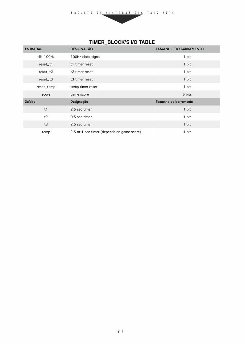
3.4 - TIMER_BLOCK
The timer_block component is composed of four timers, being these the t1, t2, t3 and temp from the finite state machine. These timers where built from the composing of one up counter and a compare block each. The up counter counts time with a 100Hz clock signal and the compare blocks verify if the desired time has been reached. When the desired time has been counted, the up counters are turned off by the “clk_en” clock enable port.
The timers t1, t2 and t3 count 2.5, 0.5 and 2.5 seconds respectively. The timer temp counts 2.5 or 1 second depending on the current score. The first case applies when the score is less then 30 points while the second case applies when the score is equal or greater then 30 points.
We can observe the adopted block composition for this component in the Timer_block Component Diagram.
The input/output description of this component can be found on the Timer_block’s I/O Table
TIMER_BLOCK COMPONENT DIAGRAM
2 0
P R O J E T O D E S I S T E M A S D I G I T A I S 2 0 1 5
TIMER_BLOCK’S I/O TABLEENTRADAS DESIGNAÇÃO TAMANHO DO BARRAMENTO
clk_100Hz 100Hz clock signal 1 bit
reset_t1 t1 timer reset 1 bit
reset_t2 t2 timer reset 1 bit
reset_t3 t3 timer reset 1 bit
reset_temp temp timer reset 1 bit
score game score 6 bits
Saídas Designação Tamanho do barramento
t1 2.5 sec timer 1 bit
t2 0.5 sec timer 1 bit
t3 2.5 sec timer 1 bit
temp 2.5 or 1 sec timer (depends on game score) 1 bit
2 1

P R O J E T O D E S I S T E M A S D I G I T A I S 2 0 1 5
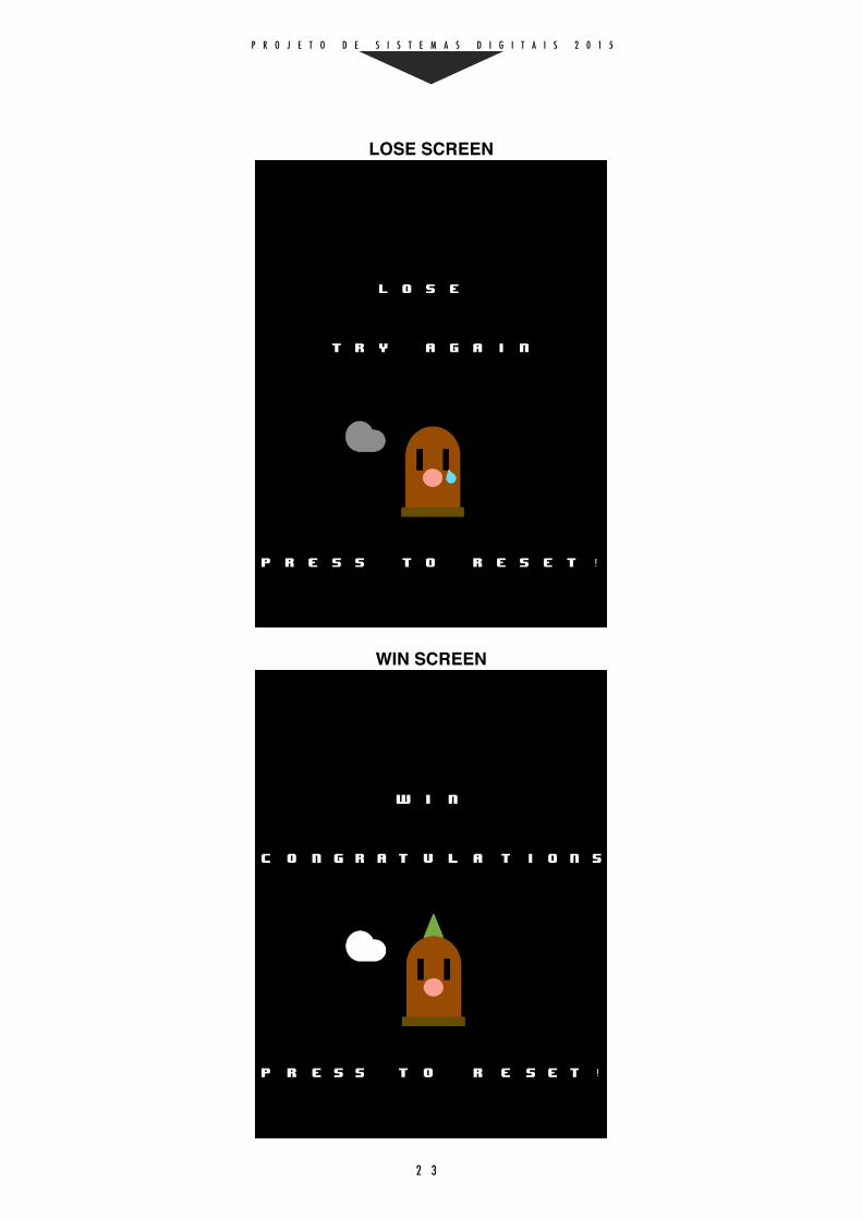
3.5 - RAMS_BLOCK
This component is the result of block combination. It contains four RAM blocks that store the address of characters from char_Rom block. One of these RAMs stores the static word “SCORE-“ followed by the dynamic game score for the Game Screen. The other three RAMs are static and store the addresses of the characters shown on the Start, Win and Lose Screen represented below. The output selection of which RAM outputs the rams_block is managed by the state of the game, knowing that the game has four Screens:
• Start Screen - an introduction message is shown;• Game Screen - where the game will be played, showing the moles and game score;• Lose Screen - a lose message is shown;• Win Screen - a win message is shown.
In this component, the output data flow is controlled with a multiplexer so that we obtain the desired output based on the finite state machine state. This control decides which RAM outputs to the char_ROM to be shown on the LCD, due to the back_box image management.
Note that the mole and the cloud on the images below are generated in back_box and not the rams_block component.
START SCREEN
2 2
P R O J E T O D E S I S T E M A S D I G I T A I S 2 0 1 5
LOSE SCREEN
WIN SCREEN
2 3
P R O J E T O D E S I S T E M A S D I G I T A I S 2 0 1 5
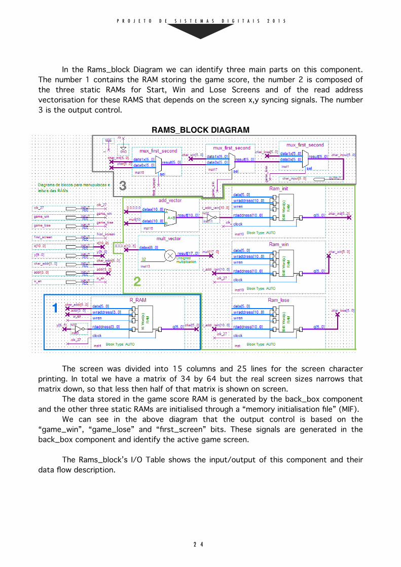
In the Rams_block Diagram we can identify three main parts on this component. The number 1 contains the RAM storing the game score, the number 2 is composed of the three static RAMs for Start, Win and Lose Screens and of the read address vectorisation for these RAMS that depends on the screen x,y syncing signals. The number 3 is the output control.
RAMS_BLOCK DIAGRAM
The screen was divided into 15 columns and 25 lines for the screen character printing. In total we have a matrix of 34 by 64 but the real screen sizes narrows that matrix down, so that less then half of that matrix is shown on screen.
The data stored in the game score RAM is generated by the back_box component and the other three static RAMs are initialised through a “memory initialisation file” (MIF).
We can see in the above diagram that the output control is based on the “game_win”, “game_lose” and “first_screen” bits. These signals are generated in the back_box component and identify the active game screen.
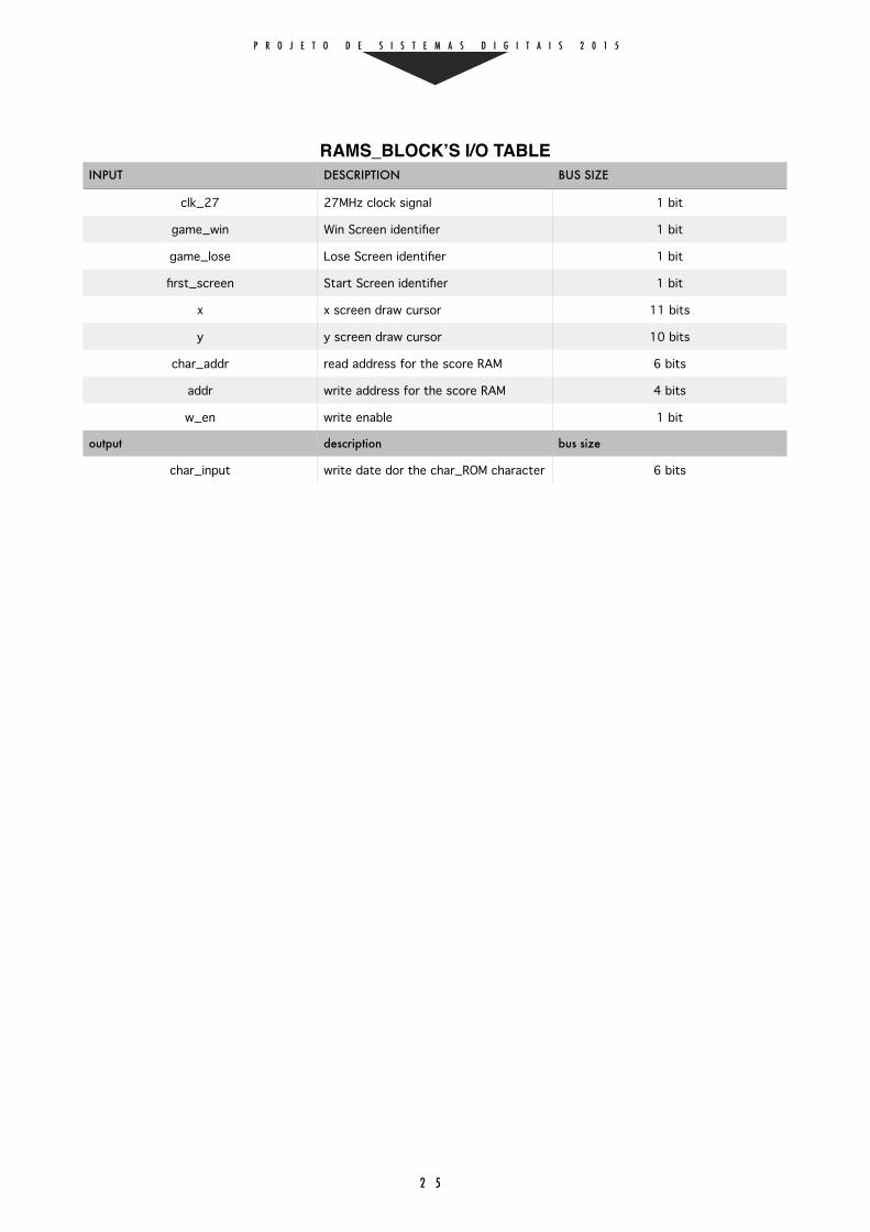
The Rams_block’s I/O Table shows the input/output of this component and their data flow description.
2 4
P R O J E T O D E S I S T E M A S D I G I T A I S 2 0 1 5
RAMS_BLOCK’S I/O TABLEINPUT DESCRIPTION BUS SIZE
clk_27 27MHz clock signal 1 bit
game_win Win Screen identifier 1 bit
game_lose Lose Screen identifier 1 bit
first_screen Start Screen identifier 1 bit
x x screen draw cursor 11 bits
y y screen draw cursor 10 bits
char_addr read address for the score RAM 6 bits
addr write address for the score RAM 4 bits
w_en write enable 1 bit
output description bus size
char_input write date dor the char_ROM character 6 bits
2 5
P R O J E T O D E S I S T E M A S D I G I T A I S 2 0 1 5
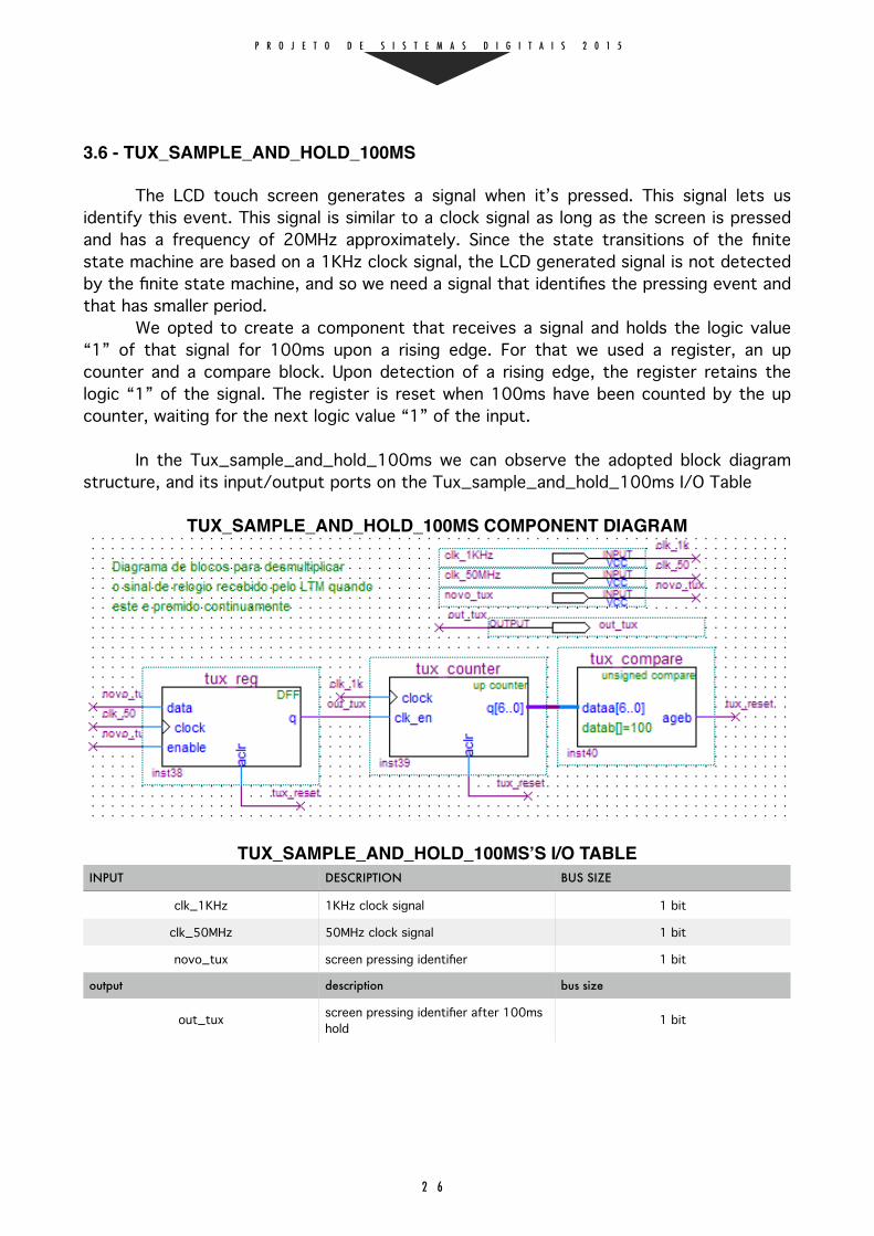
3.6 - TUX_SAMPLE_AND_HOLD_100MS
The LCD touch screen generates a signal when it’s pressed. This signal lets us identify this event. This signal is similar to a clock signal as long as the screen is pressed and has a frequency of 20MHz approximately. Since the state transitions of the finite state machine are based on a 1KHz clock signal, the LCD generated signal is not detected by the finite state machine, and so we need a signal that identifies the pressing event and that has smaller period.
We opted to create a component that receives a signal and holds the logic value “1” of that signal for 100ms upon a rising edge. For that we used a register, an up counter and a compare block. Upon detection of a rising edge, the register retains the logic “1” of the signal. The register is reset when 100ms have been counted by the up counter, waiting for the next logic value “1” of the input.
In the Tux_sample_and_hold_100ms we can observe the adopted block diagram structure, and its input/output ports on the Tux_sample_and_hold_100ms I/O Table
TUX_SAMPLE_AND_HOLD_100MS COMPONENT DIAGRAM
TUX_SAMPLE_AND_HOLD_100MS’S I/O TABLEINPUT DESCRIPTION BUS SIZE
clk_1KHz 1KHz clock signal 1 bit
clk_50MHz 50MHz clock signal 1 bit
novo_tux screen pressing identifier 1 bit
output description bus size
out_tux screen pressing identifier after 100ms hold 1 bit
2 6

P R O J E T O D E S I S T E M A S D I G I T A I S 2 0 1 5
3.7 - PSEUDO_RANDOM_GENERATOR
The game draws a mole on a random slot of a 3 by 3 grid. The slot must be random, and so a random number between 1 and 9 must be generated. The Pseudo_random_generator generates a pseudo random number between 1 and 9. It is pseudo random because it depends on a fixed frequency clock signal, but it also depends on human generated pulse, which can be considered random.
In the Pseudo_random_generator Component Diagram we can see the developed component structure.
PSEUDO_RANDOM_GENERATOR COMPONENT DIAGRAM
This component is composed of a 4bit up counter that counts from 1(binary 0001) to 9(binary 1001), being reset when the 9 value is reached. The up counter increments at a 50MHz frequency. When the signal “sample” transitions from the logic “0” value to “1” and then to “0”, the up counter current value is stored in the register.
We can observe this component’s input/output data flow in the Pseudo_random_generator I/O Table.
PSEUDO_RANDOM_GENERATOR’S I/O TABLEINPUT DESCRIPTION BUS SIZE
clk_50 50MHz clock signal 1 bit
sample number sample signal 1 bit
output description bus size
random_bits pseudo random number output 4 bits
2 7

P R O J E T O D E S I S T E M A S D I G I T A I S 2 0 1 5
4 - GAME INSTRUCTIONS
Upon the loading of the game to the DE2 board, the Start Screen is shown, containing some basic information about the game’s mechanic. Pressing this screen will lead to the Game Screen where the game starts.
In the Game Screen a green grid is shown and the game score on top of the screen. A mole will appear on a random slot of the grid. Upon clicking on the mole, it will be replaced by a coin animation on the same grid slot, lasting for 500ms. The game objective is to attain 100 point by sequentially pressing moles. Each mole pressed gives 1 point. If a mole is not pressed within 2.5 seconds from the moment it appears (for a game score of 30 or more points this window is shortened to 1 second) a Lose Screen is shown meaning the user lost the game. If the user reaches 100 points, a Win Screen is shown, meaning the user won the game.
Whether the Win Screen or the Lose Screen is active, the user can reset the game by clicking on the LCD panel. This way the Start Screen is shown again.
The mole/coin transition/animation behaviour when a mole is pressed on the Game Screen is represented in the Mole/Coin Transition Diagram. In the Game Flow Diagram we can see a full game cycle without restart.
A game explanation can be found on Youtube though the link: https://youtu.be/h-wttv1smmw
MOLE/COIN TRANSITION DIAGRAM
2 8

P R O J E T O D E S I S T E M A S D I G I T A I S 2 0 1 5
GAME FLOW DIAGRAM
2 9
W I N S C R E E N
WIN
G A M E S C R E E NS T A R T S C R E E N
L O S E S C R E E N
LOSE

P R O J E T O D E S I S T E M A S D I G I T A I S 2 0 1 5
5 - RESULTS ANALYSIS
With this project the group acquired new specific knowledge about the Terasic’s LCD touch screen module, recreating an arcade style game Whack-a-mole. The developed game corresponds to the initial expectations and even some basic animations where added to the main game's behaviour.
3 0

P R O J E T O D E S I S T E M A S D I G I T A I S 2 0 1 5
6 - CONCLUSION
6.1 - ENCOUNTERED DIFFICULTIES
The first encountered difficulty, and the one that stalled the project the longest, was the comprehension of the “Serial Peripheral Interface” (SPI) between the Altera’s DE2 and the Terasic’s LTM. We opted to manipulate the DE2_LTM_Test Terasic example that already had the SPI controller implemented. Through the manipulation of this example code we started to manipulate the screen colours, and in the final version of this block the pixel colour received is redirected to the LCD screen. This way the manipulated DE2_LTM_Test can be used in other projects with the usage of an image controller that generates the pixel colours based on the screen syncing x and y signals.
The second problem had to do with the drawing of the game score and the characters on all other game screens. For the game score drawn on the Game Screen we opted to use a dynamic RAM that changes throughout the game. This RAM is smaller and can store up to 16 words (just enough for a full horizontal screen line of characters). For all the other game screens we opted to use static RAM initialised with MIF files. We had to figure out on which horizontal and vertical sync signal values the valid screen data is sent to the screen because the screen actual image differs from the syncing signal size and doesn’t begin on the “0” sync values.
The third encountered problem was the necessity to generate a random number between 1 and 9, and the high frequency clock signal generated by the LCD screen continuous pressing. For the random number we opted for a low cost solution that is a pseudo random generator based on a fixed 50MHz clock signal and a human generated pulse. For the LCD screen pressing clock we opted to create a sampler that retains a rising edge of the signal in question for 100ms.
At last, at a final stage of the project, the lack of “embedded multiplier 9-bit elements” units from Altera’s DE2. The image generation is complex due to the high number of conditions required. As more cases where added, these high throughput elements ran lower and when all of them are in use, the Altera’s DE2 recreate similar modules with logic gate (being these slower and less efficient) which can result in timing requirements not being met, leading to failures in the application. We opted to reduce some of the implementations we had in mind and simplify the game.
6.2 - POSSIBLE IMPROVEMENTS
As a possible improvement, relative to the game mechanism, the repeated random number verifier could be improved. We detected a small glitch on the image composing when the finite state machine verifies if the new generated random hasn’t change between two consecutive states. The glitch is not very perceptive but can be eliminated.
The rest of the project objectives where reached with success and above expectations.
3 1

P R O J E T O D E S I S T E M A S D I G I T A I S 2 0 1 5
5 - ATTACHMENTS
A1 - COMB.VHD
LIBRARY IEEE;USE IEEE.STD_LOGIC_1164.all;USE IEEE.STD_LOGIC_UNSIGNED.all;USE IEEE.NUMERIC_STD.all;USE ieee.math_real.all;ENTITY comb IS
PORT( clock_1k, click, comp, temp, t1,t2,t3 :IN STD_LOGIC;f_s, s_s, lose, win, random_gen, reset_t1, reset_t2,reset_t3,reset_temp
:OUT STD_LOGIC;random_in, s :IN STD_LOGIC_VECTOR(3 DOWNTO 0);score_in :IN STD_LOGIC_VECTOR(6 DOWNTO 0);
n :OUT STD_LOGIC_VECTOR(3 DOWNTO 0):="0000";score_out :OUT STD_LOGIC_VECTOR(6 DOWNTO 0):="0000000");
END comb;
ARCHITECTURE behaviour OF comb ISSIGNAL random_old :STD_LOGIC_VECTOR(3 DOWNTO 0):="0000";SIGNAL flag,scored :STD_LOGIC:='0';SIGNAL c :STD_LOGIC_VECTOR(3 DOWNTO 0);BEGINPROCESS(clock_1k)BEGINIF(clock_1k'event AND clock_1k='1') THEN - - finite state machine
IF(s="0000")THENscored<='0';IF(click='1' AND t1='1') THEN
flag<='1';c<="0001";
ELSEc<="0000";
END IF;ELSIF(s="0001") THEN
flag<='0';scored<='1';c<="0011";
ELSIF(s="0010") THENIF(random_in=random_old) THEN
c<="0110";ELSE
flag<='1';c<="0011";
END IF;ELSIF(s="0011") THEN
IF(score_in>"1100011")THENc<="1000";
ELSEc<="0100";
END IF;
3 2

P R O J E T O D E S I S T E M A S D I G I T A I S 2 0 1 5
ELSIF(s="0100")THENflag<='0';IF(comp='1' AND click='1' AND temp='0')THEN
c<="0101";ELSIF(temp='1')THEN
c<="0111";ELSE
c<="0100";END IF;
ELSIF(s="0101") THENIF(t2='1')THEN
c<="0110";ELSE
c<="0101";END IF;
ELSIF(s="0110") THENc<="1001";
ELSIF(s="0111")THENflag<='0';IF(click='1' AND t3='1') THEN
c<="0000";ELSE
c<="0111";END IF;
ELSIF(s="1000")THENflag<='0';IF(click='1' AND t3='1') THEN
c<="0000";ELSE
c<="1000";END IF;
ELSIF(s="1001") THENc<="0010";
END IF;n<=c;CASE c IS - - output of the finite state machine
WHEN "0000" =>f_s<='1';s_s<='0';win<='0';lose<='0';random_gen<='0';reset_t1<='0';reset_t2<='1';
WHEN ("0010") =>f_s<='0';s_s<='1';win<='0';lose<='0';random_gen<='0';reset_t2<='1';
WHEN ("0011") =>f_s<='0';s_s<='1';win<='0';lose<='0';random_gen<='0';
3 3

P R O J E T O D E S I S T E M A S D I G I T A I S 2 0 1 5
reset_t2<='1';reset_t3<='1';reset_temp<='1';
WHEN ("0100") =>f_s<='0';s_s<='1';win<='0';lose<='0';random_gen<='0';reset_t2<='1';reset_t3<='1';reset_temp<='0';
WHEN ("0101") =>random_old<=random_in;f_s<='0';s_s<='1';win<='0';lose<='0';random_gen<='0';reset_t2<='0';
WHEN ("0001") =>f_s<='0';s_s<='1';win<='0';lose<='0';random_gen<='1';reset_t2<='1';
WHEN ("0110") =>f_s<='0';s_s<='1';win<='0';lose<='0';random_gen<='1';reset_t2<='1';
WHEN "0111" =>f_s<='0';s_s<='0';win<='0';lose<='1';random_gen<='0';reset_t1<='1';reset_t2<='1';reset_t3<='0';
WHEN "1000" =>f_s<='0';s_s<='0';win<='1';lose<='0';random_gen<='0';reset_t1<='1';reset_t2<='1';reset_t3<='0';
WHEN "1001" =>f_s<='0';s_s<='1';win<='0';lose<='0';
3 4

P R O J E T O D E S I S T E M A S D I G I T A I S 2 0 1 5
random_gen<='0';reset_t1<='0';reset_t2<='1';reset_t3<='0';
WHEN OTHERS => NULL;END CASE;
END IF;
END PROCESS;
PROCESS(flag) - - auxiliar process for the scoreBEGINIF(flag'event AND flag='1') THEN
IF(scored='0') THENscore_out<="0000000";
ELSIF(scored='1') THENscore_out<=score_in+1;
END IF;END IF;
END PROCESS;END behaviour;
3 5

P R O J E T O D E S I S T E M A S D I G I T A I S 2 0 1 5
A2 - BACK_BOX.VHD
LIBRARY IEEE;USE IEEE.STD_LOGIC_1164.all;USE IEEE.STD_LOGIC_UNSIGNED.all;USE IEEE.NUMERIC_STD.all;USE ieee.math_real.all;
ENTITY back_box ISPORT( clock_27, clock_100,clock_10, char_r,second_screen, win, lose : IN STD_LOGIC;
mode : IN STD_LOGIC_VECTOR(3 DOWNTO 0);x : IN STD_LOGIC_VECTOR(10 DOWNTO 0);y : IN STD_LOGIC_VECTOR(9 DOWNTO 0);x_tux : IN STD_LOGIC_VECTOR(11 DOWNTO 0);y_tux : IN STD_LOGIC_VECTOR(11 DOWNTO 0);data_r, data_g, data_b : OUT STD_LOGIC_VECTOR(7 DOWNTO 0);ram_addr : OUT STD_LOGIC_VECTOR(3 DOWNTO 0);char_addr : OUT STD_LOGIC_VECTOR(5 DOWNTO 0);score : IN STD_LOGIC_VECTOR(6 DOWNTO 0);reset_t2,t1,t3 : IN STD_LOGIC;comp :OUT STD_LOGIC:='0');
END back_box;
ARCHITECTURE behaviour OF back_box ISSIGNAL temp : STD_LOGIC_VECTOR(0 TO 3);SIGNAL s_0, s_1 : INTEGER:= 0;SIGNAL s0, s1 :STD_LOGIC_VECTOR(5 DOWNTO 0);SIGNAL animation, sentido, sentido_cloud :STD_LOGIC:= '0';SIGNAL yc, xc, y_mov, x_mov, x_cloud :INTEGER:= 0;SIGNAL y_cloud, y_cloud2 :INTEGER:=10;SIGNAL timer :INTEGER:=0;
BEGINPROCESS(clock_27)BEGIN
CASE mode IS - - screen pressing verification for comp outputWHEN "0001" =>
yc <= 110; xc <= 711;IF(y_tux > ((4096/4)*1) AND y_tux < ((4096/4)*2) AND x_tux > ((4096/3)*2)
AND x_tux < ((4096/3)*3)) THENcomp <='1';
ELSEcomp <='0';
END IF;WHEN "0010" =>
yc <= 275;xc <= 711;IF(y_tux > ((4096/4)*1) AND y_tux < ((4096/4)*2) AND x_tux > (4096/3) AND
x_tux < ((4096/3)*2)) THENcomp <='1';
ELSEcomp <='0';
END IF;WHEN "0011" =>
yc <= 440;xc <= 711;IF(y_tux > ((4096/4)*1) AND y_tux < ((4096/4)*2) AND x_tux > (0) AND x_tux <
((4096/3)*1)) THEN
3 6

P R O J E T O D E S I S T E M A S D I G I T A I S 2 0 1 5
comp <='1';ELSE
comp <='0';END IF;
WHEN "0100" => yc <= 110;xc <= 511;IF(y_tux > ((4096/4)*2) AND y_tux < ((4096/4)*3) AND x_tux > ((4096/3)*2)
AND x_tux < ((4096/3)*3)) THENcomp <='1';
ELSEcomp <='0';
END IF;WHEN "0101" =>
yc <= 275;xc <= 511;IF(y_tux > ((4096/4)*2) AND y_tux < ((4096/4)*3) AND x_tux > ((4096/3)*1)
AND x_tux < ((4096/3)*2)) THENcomp <='1';
ELSEcomp <='0';
END IF;WHEN "0110" =>
yc <= 440;xc <= 511;IF(y_tux > ((4096/4)*2) AND y_tux < ((4096/4)*3) AND x_tux > (0) AND x_tux <
((4096/3)*1)) THENcomp <='1';
ELSEcomp <='0';
END IF;WHEN "0111" =>
yc <= 110;xc <= 301;IF(y_tux > ((4096/4)*3) AND x_tux > ((4096/3)*2) AND x_tux < ((4096/3)*3))
THENcomp <='1';
ELSEcomp <='0';
END IF;WHEN "1000" =>
yc <= 275;xc <= 301;IF(y_tux > ((4096/4)*3) AND x_tux > ((4096/3)*1) AND x_tux < ((4096/3)*2))
THENcomp <='1';
ELSEcomp <='0';
END IF;WHEN "1001" =>
yc <= 440;xc <= 301;IF(y_tux > ((4096/4)*3) AND x_tux > (0) AND x_tux < ((4096/3)*1)) THEN
comp <='1';ELSE
comp <='0';END IF;
WHEN OTHERS => NULL;END CASE;
- - game_screen drawingIF (second_screen = '1' AND win='0' AND lose='0') THEN
- - desenha fundo de jogo
3 7

P R O J E T O D E S I S T E M A S D I G I T A I S 2 0 1 5
IF ( (x>813-5 AND x<813+5) OR (x>612-5 AND x<612+5) OR (x>411-5 AND x<411+5)) THEN
data_r <= x"70";data_g <= x"45";data_b <= x"13";
ELSIF ( ((y>185 AND y <195) OR (y>355 AND y<365)) AND x < 818 ) THENdata_r <= x"70";data_g <= x"45";data_b <= x"13";
ELSIF (x>817) THENIF (char_r='1' AND x > 960 AND x < 992) THEN
data_r <= x"ff";data_g <= x"ff";data_b <= x"ff";
ELSEIF ( ((to_integer(unsigned(y))-y_cloud)**2 + ((to_integer(unsigned(x)))-
(860)-x_cloud)**2 < 14**2) OR ((to_integer(unsigned(y))-y_cloud-15)**2 + ((to_integer(unsigned(x)))-(863)-x_cloud)**2 < 17**2) OR ((to_integer(unsigned(y))-y_cloud2)**2 + ((to_integer(unsigned(x)))-(910)-x_cloud)**2 < 10**2) OR ((to_integer(unsigned(y))-y_cloud2-10)**2 + ((to_integer(unsigned(x)))-(912)-x_cloud)**2 < 12**2) ) THEN
data_r <= x"ff";data_g <= x"ff";data_b <= x"ff";
ELSEdata_r <= x"00";data_g <= x"00";data_b <= x"aa";
END IF;END IF;
ELSE - - coin drawingIF(reset_t2='0') THEN
IF ((x>xc+x_mov-11 AND x<xc+x_mov+12) AND (y>yc-3 AND y<yc+2)) THEN
data_r <= x"cd";data_g <= x"85";data_b <= x"00";
ELSIF ( ((to_integer(unsigned(y))-yc)**2 + ((to_integer(unsigned(x)))-(xc+x_mov))**2 < 27**2)) THEN
data_r <= x"ff";data_g <= x"d7";data_b <= x"00";
ELSIF ( ((to_integer(unsigned(y))-yc-5)**2 + ((to_integer(unsigned(x)))-(xc+x_mov))**2 < 29**2)) THEN
data_r <= x"cd";data_g <= x"85";data_b <= x"00";
ELSEdata_r <= x"00";data_g <= x"aa";data_b <= x"00";
END IF;ELSE- - mole drawing
IF ( ((to_integer(unsigned(y))-yc-y_mov)**2 + ((to_integer(unsigned(x)))-(xc+35))**2 < 37**2) AND x >= xc+35 ) THEN
data_r <= x"99";data_g <= x"4c";data_b <= x"00";
3 8
P R O J E T O D E S I S T E M A S D I G I T A I S 2 0 1 5
E L S I F ( ( ( t o _ i n t e g e r ( u n s i g n e d ( y ) ) - y c - y _ m o v ) * * 2 + ((to_integer(unsigned(x)))-(xc-5))**2 < 14**2) ) THEN
data_r <= x"ff";data_g <= x"66";data_b <= x"66";
ELSIF (x>xc+7 AND x<xc+47) AND ((y>yc+y_mov+9 AND y<yc+y_mov+18) OR (y>yc+y_mov-18 AND y<yc+y_mov-9)) THEN
data_r <= x"00";data_g <= x"00";data_b <= x"00";
ELSIF ( (x>=xc-45) AND (x<xc+45) AND (y>yc+y_mov-37) AND (y<yc+y_mov+37) ) THEN
data_r <= x"99";data_g <= x"4c";data_b <= x"00";
ELSIF ( (x>xc-60) AND (x<xc-35) AND (y>yc-50) AND (y<yc+50) ) THENdata_r <= x"50";data_g <= x"45";data_b <= x"13";
ELSEdata_r <= x"00";data_g <= x"aa";data_b <= x"00";
END IF;END IF;
END IF;
- - win_screen drawingELSIF(win='1' AND lose='0' AND second_screen='0') THEN
IF (t3='0' AND (x<360 AND x>200)) THENdata_r <= x"00";data_g <= x"00";data_b <= x"00";
- - moleELSIF ( ((to_integer(unsigned(y))-275-y_mov)**2 + ((to_integer(unsigned(x)))-
(425+35))**2 < 37**2) AND x >= 425+35 ) THENdata_r <= x"99";data_g <= x"4c";data_b <= x"00";
- - cloudELSIF ( ((to_integer(unsigned(y))-275-y_mov)**2 + ((to_integer(unsigned(x)))-(496))**2 <
14**2) OR ((to_integer(unsigned(y))-275-y_mov)**2 + ((to_integer(unsigned(x)))-(504))**2 < 11**2) OR ((to_integer(unsigned(y))-275-y_mov)**2 + ((to_integer(unsigned(x)))-(512))**2 < 8**2) OR ((to_integer(unsigned(y))-275-y_mov)**2 + ((to_integer(unsigned(x)))-(520))**2 < 5**2) ) THEN
data_r <= x"32";data_g <= x"cd";data_b <= x"32";
- - mole contELSIF ( ((to_integer(unsigned(y))-275-y_mov)**2 + ((to_integer(unsigned(x)))-(425-5))**2
< 14**2) ) THENdata_r <= x"ff";data_g <= x"66";data_b <= x"66";
ELSIF (x>425+7 AND x<425+47) AND ((y>275+y_mov+9 AND y<275+y_mov+18) OR (y>275+y_mov-18 AND y<275+y_mov-9)) THEN
data_r <= x"00";data_g <= x"00";
3 9

P R O J E T O D E S I S T E M A S D I G I T A I S 2 0 1 5
data_b <= x"00";ELSIF ( (x>=425-45) AND (x<425+45) AND (y>275+y_mov-37) AND (y<275+y_mov+37) )
THEN data_r <= x"99";data_g <= x"4c";data_b <= x"00";
ELSIF ( (x>425-60) AND (x<425-35) AND (y>275-50) AND (y<275+50) ) THENdata_r <= x"50";data_g <= x"45";data_b <= x"13";
- - charactersELSE
IF (char_r='1') THENdata_r <= x"ff";data_g <= x"ff";data_b <= x"ff";
ELSIF ( ((to_integer(unsigned(y))-y_cloud)**2 + ((to_integer(unsigned(x)))-(470)-x_cloud)**2 < 15**2) OR ((to_integer(unsigned(y))-y_cloud-15)**2 + ((to_integer(unsigned(x)))-(473)-x_cloud)**2 < 18**2) ) THEN
data_r <= x"ff";data_g <= x"ff";data_b <= x"ff";
ELSEdata_r <= x"00";data_g <= x"00";data_b <= x"00";
END IF;END IF;
- - lose_screen drawingELSIF(lose='1' AND win='0' AND second_screen='0') THEN
- - tearIF (t3='0' AND (x<360 AND x>200)) THEN
data_r <= x"00";data_g <= x"00";data_b <= x"00";
ELSIF ( ((to_integer(unsigned(y))-253-y_mov)**2 + ((to_integer(unsigned(x)))-(420))**2 < 7**2) OR ((to_integer(unsigned(y))-254-y_mov)**2 + ((to_integer(unsigned(x)))-(424))**2 < 6**2) OR ((to_integer(unsigned(y))-256-y_mov)**2 + ((to_integer(unsigned(x)))-(428))**2 < 4**2) OR ((to_integer(unsigned(y))-258-y_mov)**2 + ((to_integer(unsigned(x)))-(432))**2 < 2**2) ) THEN
data_r <= x"00";data_g <= x"bf";data_b <= x"ff";
- - moleELSIF ( ((to_integer(unsigned(y))-275-y_mov)**2 + ((to_integer(unsigned(x)))-
(425+35))**2 < 37**2) AND x >= 425+35 ) THENdata_r <= x"99";data_g <= x"4c";data_b <= x"00";
ELSIF ( ((to_integer(unsigned(y))-275-y_mov)**2 + ((to_integer(unsigned(x)))-(425-5))**2 < 14**2) ) THEN
data_r <= x"ff";data_g <= x"66";data_b <= x"66";
ELSIF (x>425+7 AND x<425+47) AND ((y>275+y_mov+9 AND y<275+y_mov+18) OR (y>275+y_mov-18 AND y<275+y_mov-9)) THEN
data_r <= x"00";data_g <= x"00";
4 0

P R O J E T O D E S I S T E M A S D I G I T A I S 2 0 1 5
data_b <= x"00";ELSIF ( (x>=425-45) AND (x<425+45) AND (y>275+y_mov-37) AND (y<275+y_mov+37) )
THEN data_r <= x"99";data_g <= x"4c";data_b <= x"00";
ELSIF ( (x>425-60) AND (x<425-35) AND (y>275-50) AND (y<275+50) ) THENdata_r <= x"50";data_g <= x"45";data_b <= x"13";
- - charactersELSE
IF (char_r='1') THENdata_r <= x"ff";data_g <= x"ff";data_b <= x"ff";
ELSIF ( ((to_integer(unsigned(y))-y_cloud)**2 + ((to_integer(unsigned(x)))-(470)-x_cloud)**2 < 15**2) OR ((to_integer(unsigned(y))-y_cloud-15)**2 + ((to_integer(unsigned(x)))-(473)-x_cloud)**2 < 18**2) ) THEN
data_r <= x"7e";data_g <= x"7e";data_b <= x"7e";
ELSEdata_r <= x"00";data_g <= x"00";data_b <= x"00";
END IF;END IF;
- - first_screen drawingELSIF(second_screen='0' AND win='0' AND lose='0') THEN
IF (t1='0' AND (x<360 AND x>200)) THENdata_r <= x"00";data_g <= x"00";data_b <= x"00";
ELSIF ( ((to_integer(unsigned(y))-275-y_mov)**2 + ((to_integer(unsigned(x)))-(425+35))**2 < 37**2) AND x >= 425+35 ) THEN
data_r <= x"99";data_g <= x"4c";data_b <= x"00";
ELSIF ( ((to_integer(unsigned(y))-275-y_mov)**2 + ((to_integer(unsigned(x)))-(425-5))**2 < 14**2) ) THEN
data_r <= x"ff";data_g <= x"66";data_b <= x"66";
ELSIF (x>425+7 AND x<425+47) AND ((y>275+y_mov+9 AND y<275+y_mov+18) OR (y>275+y_mov-18 AND y<275+y_mov-9)) THEN
data_r <= x"00";data_g <= x"00";data_b <= x"00";
ELSIF ( (x>=425-45) AND (x<425+45) AND (y>275+y_mov-37) AND (y<275+y_mov+37) ) THEN
data_r <= x"99";data_g <= x"4c";data_b <= x"00";
ELSIF ( (x>425-60) AND (x<425-35) AND (y>275-50) AND (y<275+50) ) THENdata_r <= x"50";data_g <= x"45";
4 1

P R O J E T O D E S I S T E M A S D I G I T A I S 2 0 1 5
data_b <= x"13";ELSE
IF (char_r='1') THENdata_r <= x"ff";data_g <= x"ff";data_b <= x"ff";
ELSIF ( ((to_integer(unsigned(y))-y_cloud)**2 + ((to_integer(unsigned(x)))-(470)-x_cloud)**2 < 15**2) OR ((to_integer(unsigned(y))-y_cloud-15)**2 + ((to_integer(unsigned(x)))-(473)-x_cloud)**2 < 18**2) ) THEN
data_r <= x"ff";data_g <= x"ff";data_b <= x"ff";
ELSEdata_r <= x"00";data_g <= x"00";data_b <= x"00";
END IF;END IF;
END IF;END PROCESS;
PROCESS(clock_27) - - score RAM writing processBEGINIF(clock_27'EVENT AND clock_27='1') THEN
IF second_screen='1' THENCASE s_0 ISWHEN 0 => s0 <= O"60";WHEN 1 => s0 <= O"61";WHEN 2 => s0 <= O"62";WHEN 3 => s0 <= O"63";WHEN 4 => s0 <= O"64";WHEN 5 => s0 <= O"65";WHEN 6 => s0 <= O"66";WHEN 7 => s0 <= O"67";WHEN 8 => s0 <= O"70";WHEN 9 => s0 <= O"71";WHEN OTHERS => NULL;
END CASE;CASE s_1 IS
WHEN 0 => s1 <= O"60";WHEN 1 => s1 <= O"61";WHEN 2 => s1 <= O"62";WHEN 3 => s1 <= O"63";WHEN 4 => s1 <= O"64";WHEN 5 => s1 <= O"65";WHEN 6 => s1 <= O"66";WHEN 7 => s1 <= O"67";WHEN 8 => s1 <= O"70";WHEN 9 => s1 <= O"71";WHEN OTHERS => NULL;
END CASE;CASE temp IS
WHEN "0010" => char_addr <= O"23";WHEN "0011" => char_addr <= O"03";WHEN "0100" => char_addr <= O"17";WHEN "0101" => char_addr <= O"22";
4 2

P R O J E T O D E S I S T E M A S D I G I T A I S 2 0 1 5
WHEN "0110" => char_addr <= O"05";WHEN "0111" => char_addr <= O"55";WHEN "1000" => char_addr <= s1;WHEN "1001" => char_addr <= s0;WHEN OTHERS => char_addr <= O"40";
END CASE;temp <= temp + 1;
ELSIF (temp="1110") THENtemp <= "0000";
END IF;END IF;END PROCESS;
PROCESS(clock_27) - - score update process BEGIN
IF (score = "0000000") THENs_1 <= 0;s_0 <= 0;
ELSEs_0 <= to_integer(unsigned(score)) rem 10;s_1 <= to_integer(unsigned(score)) / 10;
END IF;END PROCESS;
- - animations PROCESS(clock_100)BEGIN
IF(clock_100'EVENT AND clock_100='1') THENIF(reset_t2='0') THEN
x_mov<=x_mov+1;ELSE
x_mov<=0;END IF;IF((second_screen='1' AND win='0' AND lose='0') OR second_screen='0') THEN
y_cloud<=y_cloud+1;IF(y_cloud>=600) THEN
y_cloud<=10;END IF;
END IF;END IF;
END PROCESS;- - animationsPROCESS(clock_10)BEGIN
IF(clock_10'EVENT AND clock_10='1') THENIF(reset_t2='1') THEN
IF(sentido='0')THENy_mov<=y_mov+2;IF(y_mov>=4)THEN
sentido<='1';END IF;
ELSEy_mov<=y_mov-2;IF(y_mov<=-4)THEN
sentido<='0';END IF;
END IF;
4 3

P R O J E T O D E S I S T E M A S D I G I T A I S 2 0 1 5
ELSEy_mov<=0;
END IF;IF((second_screen='1' AND win='0' AND lose='0') OR second_screen='0') THEN
IF(sentido_cloud='0') THENx_cloud<=x_cloud+1;IF(x_cloud>=4)THEN
sentido_cloud<='1';END IF;
ELSEx_cloud<=x_cloud-1;IF(x_cloud<=-4) THEN
sentido_cloud<='0';END IF;
END IF;y_cloud2<=y_cloud2+3;IF(y_cloud2>=600) THEN
y_cloud2<=10;END IF;
END IF;END IF;
END PROCESS;ram_addr <= temp;
END behaviour;
4 4

P R O J E T O D E S I S T E M A S D I G I T A I S 2 0 1 5
6 - REFERENCES
[1] Altera Corporation. (2012). DE2 Development and Education Board: DE2 User Manual, Version 1.6. Recovered from ftp://ftp.altera.com/up/pub/Altera_Material/12.1/Boards/DE2/DE2_User_Manual.pdf
[2] Terasic Inc. TRDB_LTM User Manual: LTM User Manual, Version 1.4.1. Recovered from http://w w w . t e r a s i c . c o m . t w / c g i - b i n / p a g e / a r c h i v e _ d o w n l o a d . p l ?Language=English&No=213&FID=b226168825c32dd5d7064e9a57f42b0b
[3] Altera Corporation. (February 2008). Cyclone II Device Handbook, Volume 1: Cyclone II Device Handbook, Recovered from https://www.altera.com/en_US/pdfs/literature/hb/cyc2/cyc2_cii5v1.pdf
[4] Peter J. Ashenden, The Student's Guide to VHDL, 1996, Morgan Kaufmann Publishers Inc.
[5] Peter J. Ashenden, The Designer's Guide to VHDL, 1996, Morgan Kaufmann Publishers Inc.
[6] Frank Scarpino, VHDL and AHDL Digital System Implementation, 1997, Prentice Hall PTR.
[7] Samir Palnitkar, Verilog HDL: A Guide to Digital Design and Synthesis 2nd Edition, 2003, Prentice Hall.
4 5

F A C U L T Y O F S C I E N C E A N D T E C H N O L O G Y
U N I V E R S I T Y O F C O I M B R A