
WG7831DELF. GENERAL MODULE REQUIREMENTS AND OPERATION..... 11 4.1.1. Absolute Maximum Ratings ........
53
-------------------------------------------------------------------------------------------------------------------------------------------------- Copyright © JORJIN TECHNOLOGIES INC. 2014 http://WWW.JORJIN.COM.TW CONFIDENTIAL a module solution provider WG7831DELF WLAN/BT Module TI WiLink8 IEEE 802.11b/g/n BT/BLE Solution Datasheet Draft 0.4 JORJIN CONFIDENTIAL
Transcript of WG7831DELF. GENERAL MODULE REQUIREMENTS AND OPERATION..... 11 4.1.1. Absolute Maximum Ratings ........
-------------------------------------------------------------------------------------------------------------------------------------------------- Copyright © JORJIN TECHNOLOGIES INC. 2014
http://WWW.JORJIN.COM.TW CONFIDENTIAL
a module solution provider
WG7831DELF WLAN/BT Module TI WiLink8 IEEE 802.11b/g/n
BT/BLE Solution
Datasheet
Draft 0.4
JORJIN
CONFIDENTIA
L
DOC No: WG7831DELF‐DTS‐D04
____________________________________________________________________________________ Copyright © JORJIN TECHNOLOGIES INC. 2014 1 http://WWW.JORJIN.COM.TW
CONFIDENTIAL
Index
1. OVERVIEW ................................................................................................................................... 4
1.1. GENERAL FEATURES ........................................................................................................................ 4
2. FUNCTIONAL FEATURES .................................................................................................................. 5
2.1. MODULE BLOCK DIAGRAM ............................................................................................................... 5 2.2. BLOCK FUNCTIONAL FEATURE ........................................................................................................... 6
2.2.1. WLAN Features ................................................................................................................... 6 2.2.2. Bluetooth Features ............................................................................................................. 7 2.2.3. BLE Features ....................................................................................................................... 7 2.2.4. ANT Features ...................................................................................................................... 7
3. MODULE OUTLINE ........................................................................................................................... 8
3.1. SIGNAL LAYOUT (TOP VIEW) ............................................................................................................. 8 3.2. PIN DESCRIPTION ........................................................................................................................... 9
4. MODULE SPECIFICATION ............................................................................................................... 11
4.1. GENERAL MODULE REQUIREMENTS AND OPERATION .......................................................................... 11 4.1.1. Absolute Maximum Ratings ............................................................................................. 11 4.1.2. Recommended Operating Conditions ............................................................................... 12
4.2. WLAN RF PERFORMANCE ............................................................................................................. 13 4.2.1. WLAN 2.4‐GHz Receiver ................................................................................................... 13 4.2.2. WLAN 2.4-GHz Transmitter ............................................................................................. 14
4.3. BLUETOOTH RF PERFORMANCE ....................................................................................................... 15 4.3.1. BT Receiver Characteristics, In‐Band Signals .................................................................... 15 4.3.2. BT Transmitter, BR ........................................................................................................... 16 4.3.3. BT Transmitter, EDR ........................................................................................................ 16 4.3.4. BT Modulation, BR .......................................................................................................... 17 4.3.5. BT Modulation, EDR ....................................................................................................... 17
4.4. BT LE RF PERFORMANCE ........................................................................................................ 18 4.4.1. BT LE Receiver Characteristics, In-Band Signals ........................................................... 18 4.4.2. BT LE Transmitter Characteristics .................................................................................. 18 4.4.3. BT LE Transmitter Characteristics .................................................................................. 19
4.5. ANT PERFORMANCE ................................................................................................................ 19 4.5.1. ANT Receiver Characteristics, In-Band Signals .............................................................. 19 4.5.2. ANT Transmitter Characteristics ..................................................................................... 20
JORJIN
CONFIDENTIA
L

DOC No: WG7831DELF‐DTS‐D04
____________________________________________________________________________________ Copyright © JORJIN TECHNOLOGIES INC. 2014 2 http://WWW.JORJIN.COM.TW
CONFIDENTIAL
4.6. POWER CONSUMPTION ..................................................................................................... 21 4.6.1. Shutdown and Sleep Currents .......................................................................................... 21 4.6.2. Operating Conditions....................................................................................................... 21 4.6.3. WLAN Power Currents .................................................................................................... 22 4.6.4. Bluetooth Currents ........................................................................................................... 22 4.6.5. Bluetooth LE Currents ..................................................................................................... 23 4.6.6. ANT Currents ................................................................................................................... 23
5. HOST INTERFACE TIMING CHARACTERISTICS ............................................................................... 24
5.1. WLAN SDIO TRANSPORT LAYER .................................................................................................... 24 5.2. SDIO TIMING SPECIFICATIONS ........................................................................................................ 25
5.2.1. SDIO Switching Characteristics – Default Rate .............................................................. 25 5.2.2. SDIO Switching Characteristics – High Rate .................................................................. 26
5.3. HCI UART SHARED TRANSPORT LAYERS FOR ALL FUNCTIONAL BLOCKS (EXCEPT WLAN) .......................... 28 5.3.1. UART 4-Wires Interface – H4 .......................................................................................... 28
5.4. UART TIMING SPECIFICATIONS ....................................................................................................... 29 5.5. BLUETOOTH CODEC‐PCM(AUDIO) TIMING SPECIFICATIONS .................................................................. 30
6. POWER MANAGEMENT................................................................................................................. 31
6.1. RESET‐POWER‐UP SYSTEM ............................................................................................................. 31 6.2. RESET‐POWER‐UP SYSTEM ............................................................................................................. 31 6.3. BLUETOOTH/BLE/ANT POWER‐UP SEQUENCE .................................................................................. 32
7. REFERENCE SCHEMATICS ................................................................................................... 33
8. CHIP ANTENNA PERFORMACE SUMMARY ................................................................................... 34
8.1. S‐PARAMETER TEST ...................................................................................................................... 34 8.2. SYSTEM INTEGRATION TEST ..................................................................................................... 35
8.2.1. Chamber Setup ................................................................................................................. 35 8.2.2. Chamber Setup ................................................................................................................. 36
8.3. DUT 2D PATTERN .................................................................................................................... 37 8.3.1. Phi=0 Pattern .................................................................................................................. 37 8.3.2. Phi=90 Pattern ................................................................................................................ 38 8.3.3. Theta=90 Pattern ............................................................................................................. 39
8.4. DUT 3D PATTERN .................................................................................................................... 40 8.4.1. 2.4GHz Pattern ................................................................................................................ 40 8.4.2. 2.45GHz Pattern .............................................................................................................. 41 8.4.3. 2.5GHz Pattern ................................................................................................................ 42
JORJIN
CONFIDENTIA
L

DOC No: WG7831DELF‐DTS‐D04
____________________________________________________________________________________ Copyright © JORJIN TECHNOLOGIES INC. 2014 3 http://WWW.JORJIN.COM.TW
CONFIDENTIAL
8.5. TOTAL EFFICIENCY ................................................................................................................... 43
9. DESIGN RECOMMENDATIONS ....................................................................................................... 44
9.1. DESIGN NOTE ON DEBUG PORT ....................................................................................................... 44 9.2. MODULE LAYOUT RECOMMENDATIONS ............................................................................................. 44
10. PACKAGE INFORMATION ............................................................................................................. 45
10.1. RECOMMENDED PAD DESIGN ........................................................................................................ 45 10.2. MODULE MECHANICAL OUTLINE ................................................................................................... 47 10.3. ORDERING INFORMATION ............................................................................................................ 48 10.4. PACKAGE MARKING .................................................................................................................... 48
11. SMT AND BAKING RECOMMENDATION ..................................................................................... 49
11.1. BAKING RECOMMENDATION ......................................................................................................... 49 11.2. SMT RECOMMENDATION ............................................................................................................ 49
12. TPAE REEL INFROMATION ........................................................................................................... 51
12.1. COVER / CARRIER TAPE DIMENSION ............................................................................................... 51
13. HISTORY CHANGE ........................................................................................................................ 52
JORJIN
CONFIDENTIA
L

DOC No: WG7831DELF‐DTS‐D04
____________________________________________________________________________________ Copyright © JORJIN TECHNOLOGIES INC. 2014 4 http://WWW.JORJIN.COM.TW
CONFIDENTIAL
1. OVERVIEW
WG7831DELF, a WiFi, BT, BLE SiP (system in package) module, is the most demanded design for all
handset and portable devices with Wilink8 solution from TI.
1.1. General Features
WLAN, Bluetooth, BLE, ANT with Integrated RF Front‐End Module (FEM), Power Amplifier (PA),
and Power Management on a Single Module
36 pin package
Dimension 25mm(L) x 25mm(W) x 2.5mm(H)
Provides efficient direct connection to battery by employing several integrated switched mode
power supplies (DC2DC).
Seamless Integration with TI Sitara™ and Other Application Processors
WLAN and BT/BLE/ANT cores are software and hardware compatible with prior WL127x and
WL128x offerings, for smooth migration to device.
Shared HCI transport for BT/BLE/ANT over UART and SDIO for WLAN.
Temperature detection and compensation mechanism ensures minimal variation in RF
performance over the entire temperature range.
BT 4.0, BLE, ANT and all audio processing features work in parallel and include full coexistence
with WLAN
Built‐in the chip Antenna.
Built‐in 26MHz crystal for fast clock, 32.786KHz oscillator for slow clock.
JORJIN
CONFIDENTIA
L
DOC No: WG7831DELF‐DTS‐D04
____________________________________________________________________________________ Copyright © JORJIN TECHNOLOGIES INC. 2014 5 http://WWW.JORJIN.COM.TW
CONFIDENTIAL
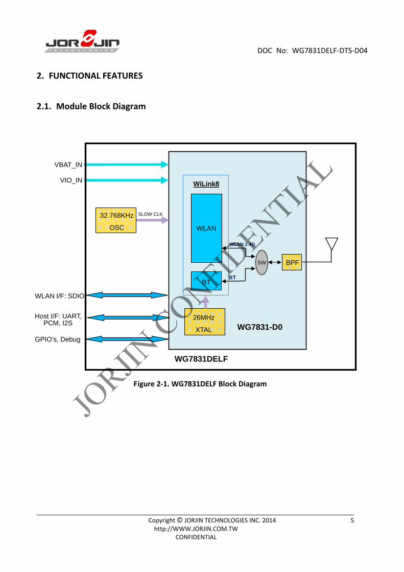
2. FUNCTIONAL FEATURES
2.1. Module Block Diagram
WLAN
BT
WiLink8
SW
WG7831-D0
VBAT_IN
VIO_IN
SLOW CLK
Host I/F: UART,
WLAN I/F: SDIO
PCM, I2S
GPIO’s, Debug
WLAN 2.4G
32.768KHz
OSC
BPF
BT
26MHz
XTAL
Figure 2‐1. WG7831DELF Block Diagram
WG7831DELF
JORJIN
CONFIDENTIA
L

DOC No: WG7831DELF‐DTS‐D04
____________________________________________________________________________________ Copyright © JORJIN TECHNOLOGIES INC. 2014 6 http://WWW.JORJIN.COM.TW
CONFIDENTIAL
2.2. Block Functional Feature
2.2.1. WLAN Features
Integrated 2.4GHz Power Amplifier (PA) for WLAN solution
WLAN Baseband Processor and RF transceiver Supporting IEEE Std 802.11b/g/n
WLAN 2.4GHz SISO (20/40 MHz channels)
Baseband Processor
- IEEE Std 802.11b/g/n data rates and IEEE Std 802.11n data rates up to 40 MHz
SISO.
Fully calibrated system. Production calibration not required.
Medium Access Controller (MAC)
Embedded ARM™ Central Processing Unit (CPU)
Hardware‐Based Encryption/Decryption using 64‐, 128‐, and 256‐Bit WEP, TKIP
or AES Keys,
Supports requirements for Wi‐Fi Protected Access (WPA and WPA2.0) and IEEE
Std 802.11i [includes hardware‐accelerated Advanced Encryption Standard
(AES)]
Designed to work with IEEE Std 802.1x
IEEE Std 802.11d,e,h,i,k,r PICS compliant.
New advanced co‐existence scheme with BT/BLE/ANT.
2.4 GHz Radio
Internal LNA and PA
Supports: IEEE Std , 802.11b, 802.11g and 802.11n
Supports 4 bit SDIO host interface, including high speed (HS) and V3 modes.
JORJIN
CONFIDENTIA
L
DOC No: WG7831DELF‐DTS‐D04
____________________________________________________________________________________ Copyright © JORJIN TECHNOLOGIES INC. 2014 7 http://WWW.JORJIN.COM.TW
CONFIDENTIAL
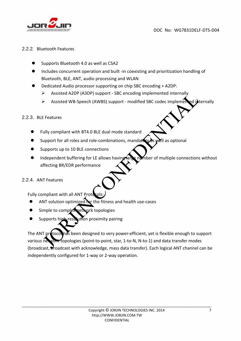
2.2.2. Bluetooth Features
Supports Bluetooth 4.0 as well as CSA2
Includes concurrent operation and built ‐in coexisting and prioritization handling of
Bluetooth, BLE, ANT, audio processing and WLAN
Dedicated Audio processor supporting on chip SBC encoding + A2DP:
Assisted A2DP (A3DP) support ‐ SBC encoding implemented internally
Assisted WB‐Speech (AWBS) support ‐ modified SBC codec implemented internally
2.2.3. BLE Features
Fully compliant with BT4.0 BLE dual mode standard
Support for all roles and role‐combinations, mandatory as well as optional
Supports up to 10 BLE connections
Independent buffering for LE allows having large number of multiple connections without
affecting BR/EDR performance
2.2.4. ANT Features
Fully compliant with all ANT Protocols:
ANT solution optimized for the fitness and health use‐cases
Simple to complex network topologies
Supports high‐resolution proximity pairing
The ANT protocol has been designed to very power‐efficient, yet is flexible enough to support
various network topologies (point‐to‐point, star, 1‐to‐N, N‐to‐1) and data transfer modes
(broadcast, broadcast with acknowledge, mass data transfer). Each logical ANT channel can be
independently configured for 1‐way or 2‐way operation.
JORJIN
CONFIDENTIA
L
DOC No: WG7831DELF‐DTS‐D04
____________________________________________________________________________________ Copyright © JORJIN TECHNOLOGIES INC. 2014 8 http://WWW.JORJIN.COM.TW
CONFIDENTIAL
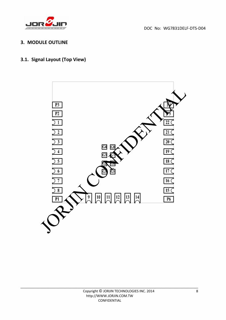
3. MODULE OUTLINE
3.1. Signal Layout (Top View)
JORJIN
CONFIDENTIA
L

DOC No: WG7831DELF‐DTS‐D04
____________________________________________________________________________________ Copyright © JORJIN TECHNOLOGIES INC. 2014 9 http://WWW.JORJIN.COM.TW
CONFIDENTIAL
3.2. Pin Description
Table 3‐1. Pin Description
Pin
No. Signal Name Type
Shut
Down
state
After
Power
Up(1)
Voltage
Level Description
1 SDIO_D2_1V8 IO HiZ HiZ 1.8V WLAN SDIO Data bit 2 (2)
2 SDIO_D0_1V8 IO HiZ HiZ 1.8V WLAN SDIO Data bit 0 (2)
3 SDIO_CLK_1V8 IN HiZ HiZ 1.8V WLAN SDIO Clock. Must be driven
by the host.
4 GND GND Ground
5 SDIO_CMD_1V8 I/O HiZ HiZ 1.8V WLAN SDIO Command (2)
6 SDIO_D1_1V8 IO HiZ HiZ 1.8V WLAN SDIO Data bit 1 (2)
7 SDIO_D3_1V8 IO HiZ PU 1.8V
WLAN SDIO Data bit 3. Changes
state to PU at WL_EN or BT_EN
assertion for card detects. Later
disabled by software during
initialization. (2)
8 WLAN_EN_1V8 IN PD PD 1.8V Mode setting: High = enable
9 BT_LINK IND IO PD PD 1.8V BT RX/TX link indicator
10 WLAN_IRQ_1V8 OUT PD 0 1.8V
SDIO available, interrupt out.
Active high. (For
WL_RS232_TX/RX pull up at
power up)
11 BT_PCM_AUD_FSYNC OUT PD PD 1.8V Bluetooth PCM/I2S Bus. Frame
sync. NC if not used.
12 BT_PCM_ AUD_CLK OUT PD PD 1.8V Bluetooth PCM/I2S Bus. Clock.
NC if not used.
13 GND GND Ground
14 BT_EN_1V8 In PD PD 1.8V Mode setting: High = enable
15 BT_PCM_ AUD_IN IN PD PD 1.8V Bluetooth PCM/I2S Bus. Data in
NC if not used.
16 BT_PCM_AUD_OUT OUT PD PD 1.8V Bluetooth PCM/I2S Bus. Data
out. NC if not used.
JORJIN
CONFIDENTIA
L

DOC No: WG7831DELF‐DTS‐D04
____________________________________________________________________________________ Copyright © JORJIN TECHNOLOGIES INC. 2014 10
http://WWW.JORJIN.COM.TW CONFIDENTIAL
17 BT_HCI_TX_1V8 OUT PU PU 1.8V UART TX to host.
NC if not used.
18 BT_HCI_RX _1V8 IN PU PU 1.8V UART RX from host.
NC if not used.
19 BT_HCI_CTS _1V8 IN PU PU 1.8V UART CTS from host.
NC if not used.
20 BT_HCI_RTS _1V8 OUT PU PU 1.8V UART RTS to host.
NC if not used.
21 VIO_IN POW 1.8V Connect to 1.8V external VIO
22 VBAT_IN POW VBAT Power supply input, 2.9 to 4.8 V
G1 GND GND Ground
G2 GND GND Ground
G3 GND GND Ground
G4 GND GND Ground
G5 GND GND Ground
G6 GND GND Ground
G7 GND GND Ground
G8 GND GND Ground
P1 GND GND Ground
P2 GND GND Ground
P3 GND GND Ground
P4 GND GND Ground
P5 GND GND Ground
P6 GND GND Ground
(1) PU=pull up; PD=pull down.
(2) Host must provide PU for all non‐CLK SDIO signals
JORJIN
CONFIDENTIA
L

DOC No: WG7831DELF‐DTS‐D04
____________________________________________________________________________________ Copyright © JORJIN TECHNOLOGIES INC. 2014 11
http://WWW.JORJIN.COM.TW CONFIDENTIAL
4. MODULE SPECIFICATION
4.1. General Module Requirements and Operation
4.1.1. Absolute Maximum Ratings
1) Stresses beyond those listed under “absolute maximum ratings” may cause permanent damage to the device.
These are stress ratings only and functional operation of the device at these or any other conditions beyond those
indicated under “operating conditions” is not implied. Exposure to absolute‐maximum‐rated conditions for extended
periods may affect device reliability.
2) 5.5V up to 10s cumulative in 7 years, 5V cumulative to 250s, 4.8V cumulative to 2.33 years ‐ all includes charging
dips and peaks.
3) Electrostatic discharge (ESD) to measure device sensitivity/immunity to damage caused by electrostatic discharges
into device.
4) Level listed is the passing level per ANSI/ESDA/JEDEC JS‐001. JEDEC document JEP155 states that 500V HBM allows
safe manufacturing with a standard ESD control process, and manufacturing with less than 500V HBM is possible if
necessary precautions are taken. Pins listed as 1000V may actually have higher performance.
5) Level listed is the passing level per EIA‐JEDEC JESD22‐C101E. JEDEC document JEP157 states that 250 V CDM allows
safe manufacturing with a standard ESD control process, and manufacturing with less than 250V CDM is possible if
necessary precautions are taken. Pins listed as 250 V may actually have higher performance
Parameter Value Units
VBAT ‐0.5 to 5.5 (2) V
VIO ‐0.5 to 2.1 V
Input voltage to all digital pins ‐0.5 to (VDD_IO + 0.5V) V
Operating ambient temperature range ‐20 to +75 °C
Storage temperature range ‐55 to +125 °C
ESD Stress Voltage (3) Human Body Model (4) >1000 V
Charged Device Model (5) >250 V
JORJIN
CONFIDENTIA
L

DOC No: WG7831DELF‐DTS‐D04
____________________________________________________________________________________ Copyright © JORJIN TECHNOLOGIES INC. 2014 12
http://WWW.JORJIN.COM.TW CONFIDENTIAL
4.1.2. Recommended Operating Conditions
Parameter Condition Sym Min Max Units
VBAT (1) DC supply range
for all modes
2.9 4.8 V
1.8 V IO ring power supply voltage 1.62 1.95
IO high‐level input voltage VIH 0.65 x VDD_IO VDD_IO
IO low‐level input voltage VIL 0 0.35 x VDD_IO
Enable inputs high‐level input
voltage
VIH_EN 1.365 VDD_IO
Enable inputs low‐level input
voltage
VIL_EN 0 0.4
High‐level output voltage @ 4 mA VOH VDD_IO ‐0.45 VDD_IO
@ 1 mA VDD_IO ‐0.112 VDD_IO
@ 0.3 mA VDD_IO ‐0.033 VDD_IO
Low‐level output voltage @ 4 mA VOL 0 0.45
@ 1 mA 0 0.112
@ 0.09 mA 0 0.01
Input transitions time Tr/Tf from
10% to 90% (Digital IO) (2)
Tr/Tf 1 10 ns
Output rise time from 10% to 90%
(Digital pins) (2)
CL < 25 pF Tr 5.3 ns
Output fall time from 10% to 90%
(Digital pins) (2)
CL < 25 pF Tf 4.9
Ambient operating temperature ‐20 75 ºC
Maximum power dissipation WLAN operation 2.8 W
BT operation 0.2
(1) 4.8V is applicable only for 2.3 years (30% of the time). Otherwise, the maximum VBAT should not exceed 4.3V.
(2) Applies to all Digital lines except SDIO, UART, I2C, PCM.
JORJIN
CONFIDENTIA
L

DOC No: WG7831DELF‐DTS‐D04
____________________________________________________________________________________ Copyright © JORJIN TECHNOLOGIES INC. 2014 13
http://WWW.JORJIN.COM.TW CONFIDENTIAL
4.2. WLAN RF Performance
4.2.1. WLAN 2.4‐GHz Receiver
Parameter Condition Min Typ Max Units
Operation frequency range 2412 2484 MHz
Sensitivity
- 20MHz Bandwidth
- At < 10% PER limit
1 Mbps DSSS ‐96.3 ‐93.4 dBm
2 Mbps DSSS ‐93.2 ‐90.5
5.5 Mbps CCK ‐90.6 ‐87.9
11 Mbps CCK ‐87.9 ‐85.7
6 Mbps OFDM ‐92 ‐89.2
9 Mbps OFDM ‐90.4 ‐87.7
12 Mbps OFDM ‐89.5 ‐86.8
18 Mbps OFDM ‐87.2 ‐84.5
24 Mbps OFDM ‐84.1 ‐81.4
36 Mbps OFDM ‐80.7 ‐78
48 Mbps OFDM ‐76.5 ‐73.8
54 Mbps OFDM ‐74.9 ‐72.4
MCS0 MM 4K ‐90.4 ‐87.4
MCS1 MM 4K ‐87.6 ‐84.9
MCS2 MM 4K ‐85.9 ‐83.2
MCS3 MM 4K ‐82.8 ‐80.1
MCS4 MM 4K ‐79.4 ‐76.7
MCS5 MM 4K ‐75.2 ‐72.5
MCS6 MM 4K ‐73.5 ‐70.8
MCS7 MM 4K ‐72.4 ‐69.7
MCS0 MM 4K 40MHz ‐87.4 ‐82.7
MCS7 MM 4K 40MHz ‐69 ‐65.5
Max Input Level
At < 10% PER limit
OFDM(11g/n) ‐19 ‐9 dBm
CCK ‐4 0 Adjacent channel rejection
Sensitivity level +3dB for OFDM, Sensitivity
level +6dB for 11b
2Mbps DSSS 42.7
dBm11Mbps CCK 37.9 54Mbps OFDM 2.0
LO Leakage ‐80 dBm
JORJIN
CONFIDENTIA
L

DOC No: WG7831DELF‐DTS‐D04
____________________________________________________________________________________ Copyright © JORJIN TECHNOLOGIES INC. 2014 14
http://WWW.JORJIN.COM.TW CONFIDENTIAL
PER Floor 1.0 2.0 %
4.2.2. WLAN 2.4-GHz Transmitter
Parameter Condition Min Typ Max
Output Power (1)
‐ Maximum RMS output power
measured at 1dB from IEEE
spectral mask or EVM
1 Mbps DSSS 15 17 – dBm
2 Mbps DSSS 15 17 –
5.5 Mbps CCK 15 17 –
11 Mbps CCK 15 17 –
6 Mbps OFDM 15 17 –
9 Mbps OFDM 15 17 –
12 Mbps OFDM 15 17 –
18 Mbps OFDM 15 17 –
24 MbpS OFDM 14 16.2 –
36 Mbps OFDM 13.1 15.3 –
48 Mbps OFDM 12.4 14.6 –
54 Mbps OFDM 11.8 13.8 –
MCS0 MM 13.9 16.1
MCS1 MM 13.9 16.1
MCS2 MM 13.9 16.1
MCS3 MM 13.9 16.1
MCS4 MM 13.3 15.3
MCS5 MM 12.4 14.6
MCS6 MM 11.8 13.8
MCS7 MM 10.6 12.6
MCS0 MM 40MHz 12.3 14.8
MCS7 MM 40MHz 10.2 12.2
Output power accuracy ‐1.5 +1.5 dB
Output power resolution 0.125 dB
Operation frequency range 2412 2484 MHz
(1) The maximum RMS output power is measured at 1dB tolerance from IEEE 802.11 spectral mask or EVM. Base
on EMC rules, the output power might need to be degraded. Due to different hardware design, possibly
degrade up to 2dB.
JORJIN
CONFIDENTIA
L

DOC No: WG7831DELF‐DTS‐D04
____________________________________________________________________________________ Copyright © JORJIN TECHNOLOGIES INC. 2014 15
http://WWW.JORJIN.COM.TW CONFIDENTIAL
4.3. Bluetooth RF Performance
4.3.1. BT Receiver Characteristics, In‐Band Signals
Parameter Condition Min Typ Max BT
Spec
Units
BT BR, EDR operation
frequency range
2402 2480 MHz
BT BR, EDR channel spacing 1 MHz
BT BR, EDR sensitivity (1)
Dirty TX on
BR, BER = 0.1% ‐88.7 ‐92.2 ‐70 dBm
EDR2, BER = 0.01% ‐87.7 ‐91.7 ‐70
EDR3, BER = 0.01% ‐80.2 ‐84.7 ‐70
BT EDR BER floor at
sensitivity + 10 dB, dirty TX
off (for 1,600,000 bits)
EDR2 1e‐6 1e‐5
EDR3 1e‐6 1e‐5
BT BR, EDR maximum
useable input power
BR, BER = 0.1% ‐5 ‐20 dBm
EDR2, BER = 0.1% ‐10 ‐20
EDR3, BER = 0.1% ‐10 ‐20
BT BR intermodulation Level of interferers For n = 3, 4, and 5 ‐36.0 ‐30.0 ‐39 dBm
BT BR, EDR C/I performance
Numbers show
wanted‐signal to
interfering‐signal ratio.
Smaller numbers indicate
better C/I performances
(Image frequency = ‐1MHz)
BR, Co‐channel 8.0 10.0 11 dB
EDR, Co‐channel EDR2 9.5 12.0 13
EDR3 16.5 20.0 21
BR, adjacent ±1 MHz ‐10.0 ‐3.0 0
EDR, adjacent ±1 MHz,
(image)
EDR2 ‐10.0 ‐3.0 0
EDR3 ‐5.0 2.0 5
BR, adjacent +2 MHz ‐38.0 ‐33.0 ‐30
EDR, adjacent +2 MHz, EDR2 ‐38.0 ‐33.0 ‐30
EDR3 ‐38.0 ‐28.0 ‐25
BR, adjacent ‐2 MHz ‐28.0 ‐20.0 ‐20
EDR, adjacent
‐2 MHz
EDR2 ‐28.0 ‐20.0 ‐20
EDR3 ‐22.0 ‐13.0 ‐13
JORJIN
CONFIDENTIA
L

DOC No: WG7831DELF‐DTS‐D04
____________________________________________________________________________________ Copyright © JORJIN TECHNOLOGIES INC. 2014 16
http://WWW.JORJIN.COM.TW CONFIDENTIAL
BR, adjacent ≥Ι±3Ι MHz ‐45.0 ‐42.0 ‐40
EDR, adjacent ≥Ι±3Ι
MHz
EDR2 ‐45.0 ‐42.0 ‐40
EDR3 ‐44.0 ‐36.0 ‐33
BT BR, EDR RF return loss ‐10.0 dB
(1) Sensitivity degradation up to ‐3dB may occur due to fast clock harmonics with dirty TX on.
4.3.2. BT Transmitter, BR
Parameter Min Typ Max BT Spec Units
BR RF output power (1) VBAT >= 3V 10.7 12.7 dBm
VBAT < 3V 5.2 7.2
BR Gain Control Range 30 dB
BR Power Control Step 2 5 8 2 to 8
BR Adjacent Channel Power |M‐N| = 2 (2) ‐43.0 ‐35.0 ≤ ‐20 dBm
BR Adjacent Channel Power |M‐N| > 2 (2) ‐48.0 ‐40.0 ≤ ‐40
1) Values reflect maximum power. Reduced power is available using a vendor‐specific (VS) command.
2) Assumes 3dB insertion loss on external filter and traces
4.3.3. BT Transmitter, EDR
Parameter Min Typ Max BT Spec Units
EDR output power (1) VBAT >= 3V 5.2 7.2 dBm
VBAT < 3V 3.2 5.2
EDR relative power ‐2 1 ‐4 to +1 dB
EDR Gain Control Range 30 dB
EDR Power Control Step 2 5 8 2 to 8 dB
EDR Adjacent Channel Power |M‐N| = 1 (2) ‐36 ‐30 ≤ ‐26 dBc
EDR Adjacent Channel Power |M‐N| = 2 (2) ‐30 ‐23 ≤ ‐20 dBm
EDR Adjacent Channel Power |M‐N| > 2 (2) ‐42 ‐40 ≤ ‐40
1) Values reflect maximum power. Reduced power is available using a vendor‐specific (VS) command.
2) Assumes 3dB insertion loss on external filter and traces.
JORJIN
CONFIDENTIA
L

DOC No: WG7831DELF‐DTS‐D04
____________________________________________________________________________________ Copyright © JORJIN TECHNOLOGIES INC. 2014 17
http://WWW.JORJIN.COM.TW CONFIDENTIAL
4.3.4. BT Modulation, BR
Parameter Condition(1) Performances BT
specUnits
Min Typ Max
BR ‐20dB Bandwidth 925 995 ≤1000 kHz
BR modulation
characteristics
∆f1avg Mod data = 4‐ones,
4‐zeros: 111100001111...
145 160 170 140 to
175 kHz
∆f2max ≥ limit for
at least 99.9% of all
Δf2max
Mod data = 1010101...
120
130
> 115
kHz
∆f2avg / ∆f1avg 85 88 > 80 %
BR carrier frequency
drift
One slot packet ‐25 +25 < ±25 kHz
Three and five slot packet ‐35 35 < ±40 kHz
BR drift rate lfk+5 – fkl , k = 0 …. max 15 < 20 kHz/
50μs
BR initial carrier
frequency tolerance (2) f0 – fTX ‐25 25 < ±75 kHz
1) Performance figures at maximum power
2) This number is added on top of the reference clock frequency accuracy
4.3.5. BT Modulation, EDR
Parameter (1) Condition Min Typ. Max BT spec Units
EDR Carrier frequency stability ‐5 5 ≤10 kHz
EDR Initial Carrier Frequency Tolerance (2) ‐25 25 ±75 kHz
EDR RMS DEVM EDR2 4 15 20 %
EDR3 4 10 13 %
EDR 99% DEVM EDR2 30 30 %
EDR3 20 20 %
EDR Peak DEVM EDR2 9 25 35 %
EDR3 9 18 25 %
1) Performance figures at maximum power
2) This number is added on top of the reference clock frequency accuracy
JORJIN
CONFIDENTIA
L
DOC No: WG7831DELF‐DTS‐D04
____________________________________________________________________________________ Copyright © JORJIN TECHNOLOGIES INC. 2014 18
http://WWW.JORJIN.COM.TW CONFIDENTIAL
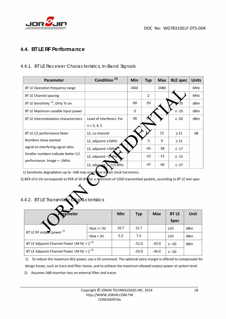
4.4. BT LE RF Performance
4.4.1. BT LE Receiver Characteristics, In-Band Signals
Parameter Condition (2) Min Typ Max BLE spec Units
BT LE Operation frequency range 2402 2480 MHz
BT LE Channel spacing 2 MHz
BT LE Sensitivity (1), Dirty Tx on ‐90 ‐93 ≤ ‐70 dBm
BT LE Maximum useable input power ‐5 ≥ ‐10 dBm
BT LE Intermodulation characteristics Level of interferers. For
n = 3, 4, 5
‐36 ‐30 ≥ ‐50 dBm
BT LE C/I performance Note:
Numbers show wanted
signal‐to‐interfering signal ratio.
Smaller numbers indicate better C/I
performance. Image = ‐1MHz
LE, co‐channel 8 12 ≤ 21 dB
LE, adjacent ±1MHz ‐5 0 ≤ 15
LE, adjacent +2MHz ‐45 ‐38 ≤ ‐17
LE, adjacent –2MHz ‐22 ‐15 ≤ ‐15
LE, adjacent ≥ |±3|MHz ‐47 ‐40 ≤ ‐27
1) Sensitivity degradation up to ‐3dB may occur due to fast clock harmonics.
2) BER of 0.1% corresponds to PER of 30.8% for a minimum of 1500 transmitted packets, according to BT LE test spec
4.4.2. BT LE Transmitter Characteristics
Parameter Min Typ Max BT LE
Spec
Unit
BT LE RF output power (1) Vbat >= 3V 10.7 12.7 ≤10 dBm
Vbat < 3V 5.2 7.2 ≤10 dBm
BT LE Adjacent Channel Power |M‐N| = 2 (2) ‐51.0 ‐43.0 ≤ –20 dBm
BT LE Adjacent Channel Power |M‐N| > 2 (2) ‐54.0 ‐46.0 ≤ –30
1) To reduce the maximum BLE power, use a VS command. The optional extra margin is offered to compensate for
design losses, such as trace and filter losses, and to achieve the maximum allowed output power at system level.
2) Assumes 3dB insertion loss on external filter and traces
JORJIN
CONFIDENTIA
L
DOC No: WG7831DELF‐DTS‐D04
____________________________________________________________________________________ Copyright © JORJIN TECHNOLOGIES INC. 2014 19
http://WWW.JORJIN.COM.TW CONFIDENTIAL
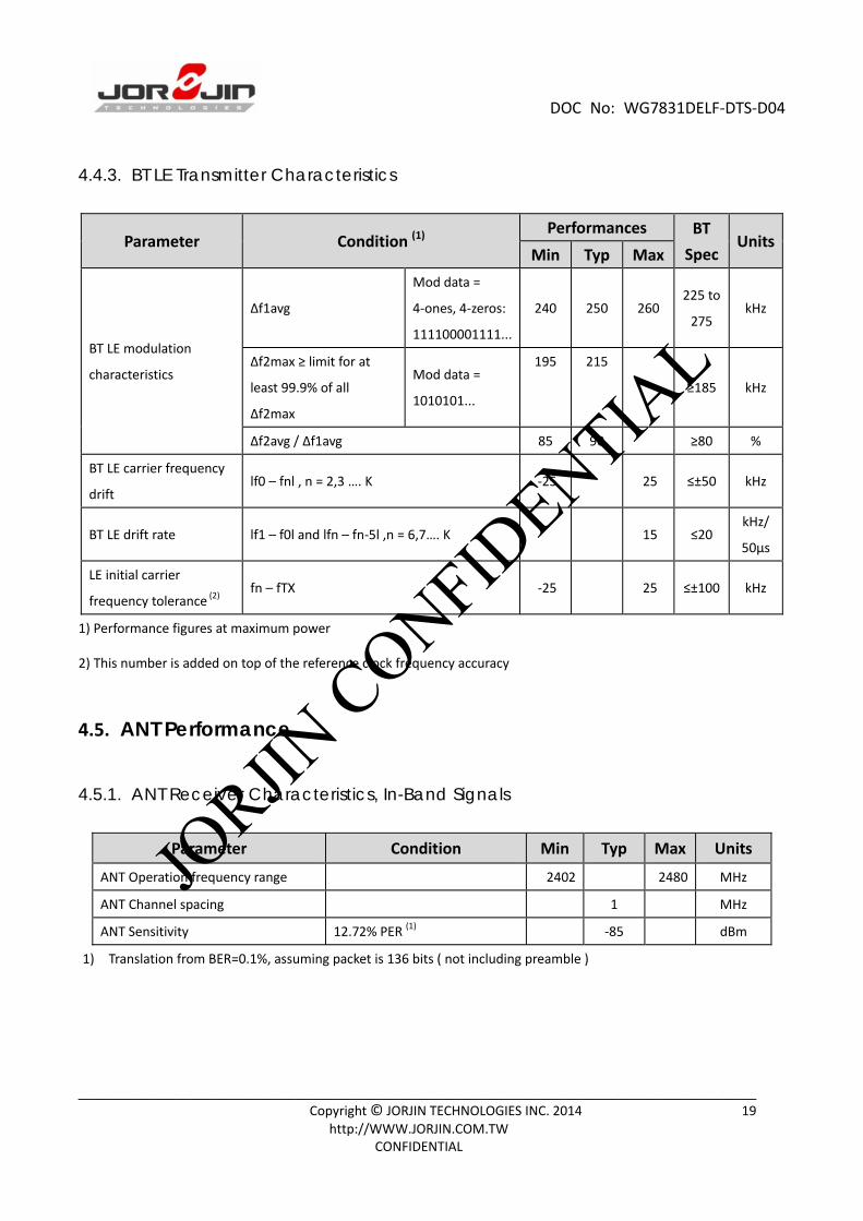
4.4.3. BT LE Transmitter Characteristics
Parameter Condition (1) Performances BT
SpecUnits
Min Typ Max
BT LE modulation
characteristics
∆f1avg
Mod data =
4‐ones, 4‐zeros:
111100001111...
240
250
260 225 to
275 kHz
∆f2max ≥ limit for at
least 99.9% of all
Δf2max
Mod data =
1010101...
195 215 ≥185 kHz
∆f2avg / ∆f1avg 85 90 ≥80 %
BT LE carrier frequency
drift lf0 – fnl , n = 2,3 …. K ‐25 25 ≤±50 kHz
BT LE drift rate lf1 – f0l and lfn – fn‐5l ,n = 6,7…. K 15 ≤20 kHz/
50μs
LE initial carrier
frequency tolerance (2) fn – fTX ‐25 25 ≤±100 kHz
1) Performance figures at maximum power
2) This number is added on top of the reference clock frequency accuracy
4.5. ANT Performance
4.5.1. ANT Receiver Characteristics, In-Band Signals
Parameter Condition Min Typ Max Units
ANT Operation frequency range 2402 2480 MHz
ANT Channel spacing 1 MHz
ANT Sensitivity 12.72% PER (1) ‐85 dBm
1) Translation from BER=0.1%, assuming packet is 136 bits ( not including preamble )
JORJIN
CONFIDENTIA
L

DOC No: WG7831DELF‐DTS‐D04
____________________________________________________________________________________ Copyright © JORJIN TECHNOLOGIES INC. 2014 20
http://WWW.JORJIN.COM.TW CONFIDENTIAL
4.5.2. ANT Transmitter Characteristics
Same as Bluetooth BR Transmitter Characteristics
JORJIN
CONFIDENTIA
L

DOC No: WG7831DELF‐DTS‐D04
____________________________________________________________________________________ Copyright © JORJIN TECHNOLOGIES INC. 2014 21
http://WWW.JORJIN.COM.TW CONFIDENTIAL
4.6. POWER CONSUMPTION
4.6.1. Shutdown and Sleep Currents
Parameter Power Supply Current Typ Max. Unit
Shutdown mode
All functions shut down.
VBAT 10 15 uA
VIO 2 3
WLAN sleep mode VBAT 160 340
BT sleep mode VBAT 110 285
4.6.2. Operating Conditions
Parameter Power Supply Current Typ Max. Unit
Connected IDEL VBAT 750 960 uA
VIO(1) VIO 40 450 uA
1) VIO quoted for operational IO’s (WLAN + BT IF) without debug IO.
JORJIN
CONFIDENTIA
L

DOC No: WG7831DELF‐DTS‐D04
____________________________________________________________________________________ Copyright © JORJIN TECHNOLOGIES INC. 2014 22
http://WWW.JORJIN.COM.TW CONFIDENTIAL
4.6.3. WLAN Power Currents
Parameter Conditions Typ (avg) Max. Units
LPM 2.4GHz RX LPM 49 61 mA
Receiver
2.4GHz RX search SISO20 54 66 mA
2.4GHz RX search SISO40 59 72 mA
2.4GHz RX 20M SISO 11CCK 56 72 mA
2.4GHz RX 20M SISO 6OFDM 61 72 mA
2.4GHz RX 20M SISO MCS7 65 77 mA
2.4GHz RX 40MHz MCS7 77 90 mA
Transmitter
2.4GHz TX 20M SISO 6OFDM 16dBm 285 374 mA
2.4GHz TX 20M SISO 11CCK 16dBm 273 357 mA
2.4GHz TX 20M SISO 54OFDM 12.8dBm 247 328 mA
2.4GHz TX 20M SISO MCS7 11.6dBm 238 321 mA
2.4GHz TX 40M SISO MCS7 11.2dBm 243 329 mA
4.6.4. Bluetooth Currents
Current measurements are done at the following output power: BR at 12.5dBm, EDR at 7dBm.
Use Case (1) Typ Units
BR Voice HV3 + sniff 11.6 mA
EDR Voice 2‐EV3 no retrans. + sniff 5.9 mA
Sniff 1 attempt 1.28s 178 uA
EDR A2DP EDR2 (master). SBC high quality – 345Kbs 10.4 mA
EDR A2DP EDR2 (master). MP3 high quality – 192Kbs 7.5 mA
Full throughput ACL RX: RX‐2DH5 (2) (3) 18 mA
Full throughput BR ACL TX: TX‐DH5 (3) 50 mA
Full throughput EDR ACL TX: TX‐2DH5 (3) 33 mA
Page or inquiry 1.28s/11.25ms 253 uA
P&I Scan (P=1.28/I=2.56) 332 uA
1) BT role in all scenarios is Slave, except for A2DP
2) ACL RX has same current in all modulations
3) Full throughput assumed data transfer in one direction
JORJIN
CONFIDENTIA
L

DOC No: WG7831DELF‐DTS‐D04
____________________________________________________________________________________ Copyright © JORJIN TECHNOLOGIES INC. 2014 23
http://WWW.JORJIN.COM.TW CONFIDENTIAL
4.6.5. Bluetooth LE Currents
All current measurements are done at output power of 8dBm
Use Case Typ Units
Advertising, non‐connectable (1) 131 uA
Advertising, discoverable (1) 143 uA
Scanning (2) 266 uA
Connected, master role, 1.28sec conn. Interval (3) 124 uA
Connected, slave role, 1.28sec conn. Interval (3) 132 uA
1) Advertising in all 3 channels, 1.28sec advertising interval, 15 Bytes advertise data.
2) Listening to a single frequency per window, 1.28sec scan interval, 11.25msec scan window.
3) Zero Slave connection latency Empty Tx/Rx LL packets.
4.6.6. ANT Currents
Use Case Conditions Typ Units
ANT Rx message mode 250ms interval 360 uA
ANT Rx message mode 500ms interval 220 uA
ANT Rx message mode 1000ms interval 150 uA
JORJIN
CONFIDENTIA
L
DOC No: WG7831DELF‐DTS‐D04
____________________________________________________________________________________ Copyright © JORJIN TECHNOLOGIES INC. 2014 24
http://WWW.JORJIN.COM.TW CONFIDENTIAL
5. HOST INTERFACE TIMING CHARACTERISTICS
The following table summarizes the Host Controller interface options. All interfaces operate
independently.
WLAN Shared HCI for all functional
blocks except WLAN
BT Voice/Audio
WLAN HS SDIO Over UART BT PCM
The device incorporates UART module dedicated to the BT shared‐transport Host Controller
Interface (HCI) transport layer. The HCI interface is used to transport commands, events and ACL
between the Bluetooth device and its host using HCI data packets. This acts as a shared transport
for all functional blocks except WLAN.
5.1. WLAN SDIO Transport Layer
The SDIO is the host interface for WLAN and supports a maximum clock rate of 50MHz.
The Device SDIO also supports the following features of the SDIO V3 specification:
4 bit data bus
Synchronous and Asynchronous In‐Band‐Interrupt
Default and High‐Speed (50MHz) timing
Sleep/wake commands
JORJIN
CONFIDENTIA
L

DOC No: WG7831DELF‐DTS‐D04
____________________________________________________________________________________ Copyright © JORJIN TECHNOLOGIES INC. 2014 25
http://WWW.JORJIN.COM.TW CONFIDENTIAL
5.2. SDIO Timing Specifications
5.2.1. SDIO Switching Characteristics – Default Rate
Figure 5‐1. SDIO default input timing
Figure 5‐2. SDIO default output timing
JORJIN
CONFIDENTIA
L

DOC No: WG7831DELF‐DTS‐D04
____________________________________________________________________________________ Copyright © JORJIN TECHNOLOGIES INC. 2014 26
http://WWW.JORJIN.COM.TW CONFIDENTIAL
Table 5‐1. SDIO Default Timing Characteristics(1)
PARAMETER(2) MIN MAX UNIT
Fclock Clock frequency, CLK 0 26 MHz
DC Low/high duty cycle 40 60 %
tTLH Rise time, CLK 10 ns
tTHL Fall time, CLK 10 ns
tISU Setup time, input valid before CLK↑ 3 ns
tIH Hold time, input valid after CLK↑ 2 ns
tODLY Delay time, CLK↓ to output valid 2.5 14.8 ns
CI Capacitive load on outputs 15 pF
(1) To change the data out clock edge from the falling edge (default) to the rising edge, set the configuration bit.
(2) Parameter values reflect maximum clock frequency.
5.2.2. SDIO Switching Characteristics – High Rate
Figure 5‐3. SDIO HS input timing
JORJIN
CONFIDENTIA
L

DOC No: WG7831DELF‐DTS‐D04
____________________________________________________________________________________ Copyright © JORJIN TECHNOLOGIES INC. 2014 27
http://WWW.JORJIN.COM.TW CONFIDENTIAL
Figure 5‐4. SDIO HS output timing
Table 5‐2. SDIO HS Timing Characteristics PARAMETER MIN MAX UNIT
Fclock Clock frequency, CLK 0 50 MHz
DC Low/high duty cycle 40 60 %
tTLH Rise time, CLK 3 ns
tTHL Fall time, CLK 3 ns
tISU Setup time, input valid before CLK↑ 3 ns
tIH Hold time, input valid after CLK↑ 2 ns
tODLY Delay time, CLK↓ to output valid 2.5 14 ns
CI Capacitive load on outputs 10 pF
JORJIN
CONFIDENTIA
L
DOC No: WG7831DELF‐DTS‐D04
____________________________________________________________________________________ Copyright © JORJIN TECHNOLOGIES INC. 2014 28
http://WWW.JORJIN.COM.TW CONFIDENTIAL
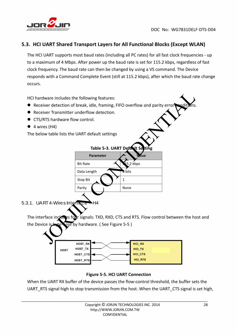
5.3. HCI UART Shared Transport Layers for All Functional Blocks (Except WLAN)
The HCI UART supports most baud rates (including all PC rates) for all fast clock frequencies ‐ up
to a maximum of 4 Mbps. After power up the baud rate is set for 115.2 kbps, regardless of fast
clock frequency. The baud rate can then be changed by using a VS command. The Device
responds with a Command Complete Event (still at 115.2 kbps), after which the baud rate change
occurs.
HCI hardware includes the following features:
Receiver detection of break, idle, framing, FIFO overflow and parity error conditions.
Receiver Transmitter underflow detection.
CTS/RTS hardware flow control. 4 wires (H4)
The below table lists the UART default settings
Table 5‐3. UART Default Setting
Parameter Value
Bit Rate 115.2 kbps
Data Length 8 bits
Stop Bit 1
Parity None
5.3.1. UART 4-Wires Interface – H4
The interface includes four signals: TXD, RXD, CTS and RTS. Flow control between the host and
the Device is byte‐wise by hardware. ( See Figure 5‐5 )
Figure 5‐5. HCI UART Connection
When the UART RX buffer of the device passes the flow‐control threshold, the buffer sets the
UART_RTS signal high to stop transmission from the host. When the UART_CTS signal is set high,
JORJIN
CONFIDENTIA
L
DOC No: WG7831DELF‐DTS‐D04
____________________________________________________________________________________ Copyright © JORJIN TECHNOLOGIES INC. 2014 29
http://WWW.JORJIN.COM.TW CONFIDENTIAL
the device stops transmitting on the interface. If HCI_CTS is set high in the middle of transmitting
a byte, the device finishes transmitting the byte and stops the transmission.
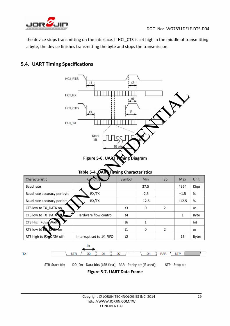
5.4. UART Timing Specifications
Figure 5‐6. UART Timing Diagram
Table 5‐4. UART Timing Characteristics Characteristic Condition Symbol Min Typ Max Unit
Baud rate 37.5 4364 Kbps
Baud rate accuracy per byte RX/TX ‐2.5 +1.5 %
Baud rate accuracy per bit RX/TX ‐12.5 +12.5 %
CTS low to TX_DATA on t3 0 2 us
CTS low to TX_DATA off Hardware flow control t4 1 Byte
CTS High Pulse Width t6 1 bit
RTS low to RX_DATA on t1 0 2 us
RTS high to RX_DATA off Interrupt set to 1/4 FIFO t2 16 Bytes
STR‐Start bit; D0..Dn ‐ Data bits (LSB first); PAR ‐ Parity bit (if used); STP ‐ Stop bit
Figure 5‐7. UART Data Frame
JORJIN
CONFIDENTIA
L
DOC No: WG7831DELF‐DTS‐D04
____________________________________________________________________________________ Copyright © JORJIN TECHNOLOGIES INC. 2014 30
http://WWW.JORJIN.COM.TW CONFIDENTIAL
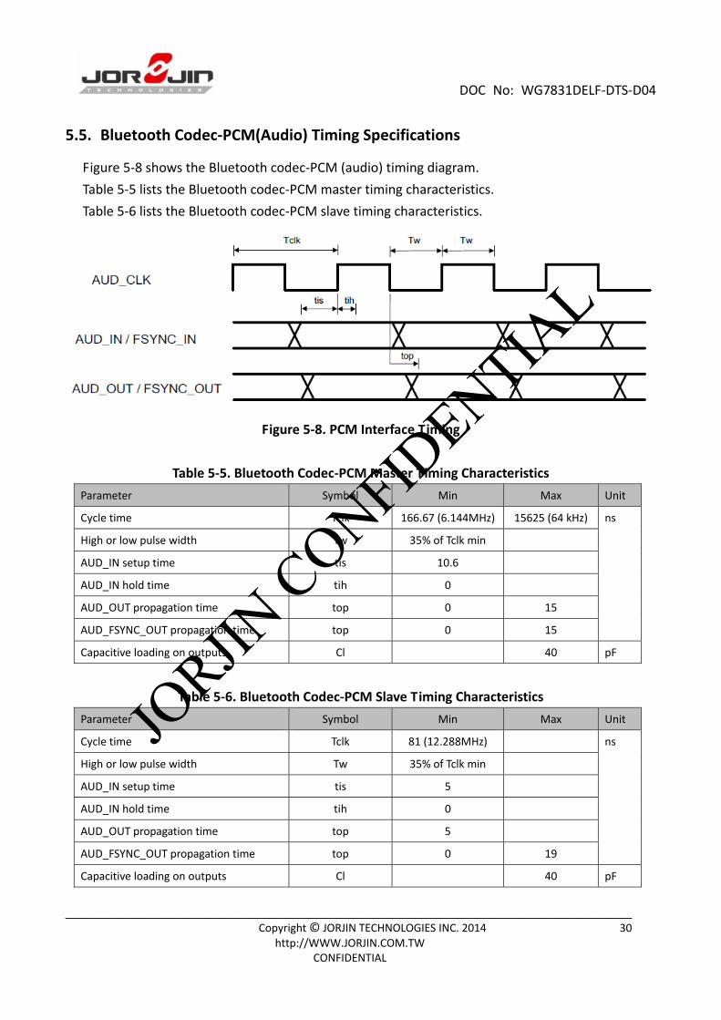
5.5. Bluetooth Codec‐PCM(Audio) Timing Specifications
Figure 5‐8 shows the Bluetooth codec‐PCM (audio) timing diagram.
Table 5‐5 lists the Bluetooth codec‐PCM master timing characteristics.
Table 5‐6 lists the Bluetooth codec‐PCM slave timing characteristics.
Figure 5‐8. PCM Interface Timing
Table 5‐5. Bluetooth Codec‐PCM Master Timing Characteristics
Parameter Symbol Min Max Unit
Cycle time Tclk 166.67 (6.144MHz) 15625 (64 kHz) ns
High or low pulse width Tw 35% of Tclk min
AUD_IN setup time tis 10.6
AUD_IN hold time tih 0
AUD_OUT propagation time top 0 15
AUD_FSYNC_OUT propagation time top 0 15
Capacitive loading on outputs Cl 40 pF
Table 5‐6. Bluetooth Codec‐PCM Slave Timing Characteristics Parameter Symbol Min Max Unit
Cycle time Tclk 81 (12.288MHz) ns
High or low pulse width Tw 35% of Tclk min
AUD_IN setup time tis 5
AUD_IN hold time tih 0
AUD_OUT propagation time top 5
AUD_FSYNC_OUT propagation time top 0 19
Capacitive loading on outputs Cl 40 pF
JORJIN
CONFIDENTIA
L

DOC No: WG7831DELF‐DTS‐D04
____________________________________________________________________________________ Copyright © JORJIN TECHNOLOGIES INC. 2014 31
http://WWW.JORJIN.COM.TW CONFIDENTIAL
6. POWER MANAGEMENT
6.1. Reset‐Power‐Up System
After VBAT and VIO are fed to the device and while BT_EN and WL_EN are deasserted (low), the
device is in SHUTDOWN state, during which functional blocks, internal DC‐DCs, and LDOs are
disabled. The power supplied to the functional blocks is cut off. When one of the signals (BT_EN or
WL_EN) are asserted (high), a power‐on reset (POR) is performed. Stable slow clock, VIO, and VBAT
are prerequisites for a successful POR.
6.2. Reset‐Power‐Up System
Figure 6‐1 shows the WLAN power‐up sequence.
Figure 6‐1. WLAN Power‐Up Sequence
JORJIN
CONFIDENTIA
L
DOC No: WG7831DELF‐DTS‐D04
____________________________________________________________________________________ Copyright © JORJIN TECHNOLOGIES INC. 2014 32
http://WWW.JORJIN.COM.TW CONFIDENTIAL
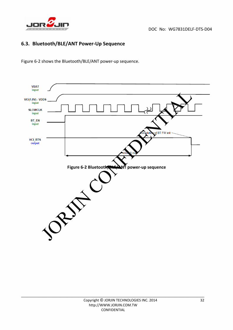
6.3. Bluetooth/BLE/ANT Power‐Up Sequence
Figure 6‐2 shows the Bluetooth/BLE/ANT power‐up sequence.
Figure 6‐2 Bluetooth/BLE/ANT power‐up sequence
JORJIN
CONFIDENTIA
L

DOC No: WG7831DELF‐DTS‐D04
____________________________________________________________________________________ Copyright © JORJIN TECHNOLOGIES INC. 2014 33
http://WWW.JORJIN.COM.TW CONFIDENTIAL
7. REFERENCE SCHEMATICS
JORJIN
CONFIDENTIA
L

DOC No: WG7831DELF‐DTS‐D04
____________________________________________________________________________________ Copyright © JORJIN TECHNOLOGIES INC. 2014 34
http://WWW.JORJIN.COM.TW CONFIDENTIAL
8. CHIP ANTENNA PERFORMACE SUMMARY
8.1. S‐Parameter Test
JORJIN
CONFIDENTIA
L

DOC No: WG7831DELF‐DTS‐D04
____________________________________________________________________________________ Copyright © JORJIN TECHNOLOGIES INC. 2014 35
http://WWW.JORJIN.COM.TW CONFIDENTIAL
8.2. System Integration Test
8.2.1. Chamber Setup
JO
RJIN CONFID
ENTIAL

DOC No: WG7831DELF‐DTS‐D04
____________________________________________________________________________________ Copyright © JORJIN TECHNOLOGIES INC. 2014 36
http://WWW.JORJIN.COM.TW CONFIDENTIAL
8.2.2. Chamber Setup
JORJIN
CONFIDENTIA
L

DOC No: WG7831DELF‐DTS‐D04
____________________________________________________________________________________ Copyright © JORJIN TECHNOLOGIES INC. 2014 37
http://WWW.JORJIN.COM.TW CONFIDENTIAL
8.3. DUT 2D Pattern
8.3.1. Phi=0 Pattern
JORJIN
CONFIDENTIA
L
DOC No: WG7831DELF‐DTS‐D04
____________________________________________________________________________________ Copyright © JORJIN TECHNOLOGIES INC. 2014 38
http://WWW.JORJIN.COM.TW CONFIDENTIAL
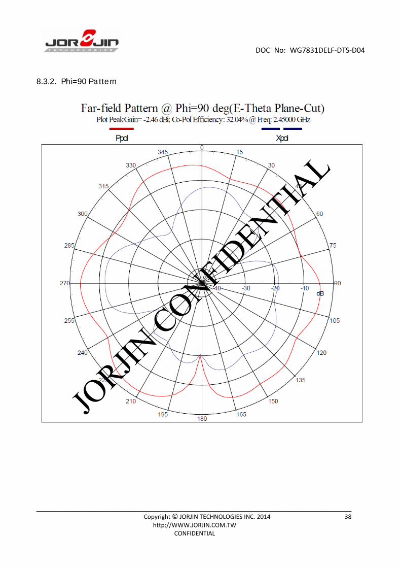
8.3.2. Phi=90 Pattern
JORJIN
CONFIDENTIA
L

DOC No: WG7831DELF‐DTS‐D04
____________________________________________________________________________________ Copyright © JORJIN TECHNOLOGIES INC. 2014 39
http://WWW.JORJIN.COM.TW CONFIDENTIAL
8.3.3. Theta=90 Pattern
JORJIN
CONFIDENTIA
L

DOC No: WG7831DELF‐DTS‐D04
____________________________________________________________________________________ Copyright © JORJIN TECHNOLOGIES INC. 2014 40
http://WWW.JORJIN.COM.TW CONFIDENTIAL
8.4. DUT 3D Pattern
8.4.1. 2.4GHz Pattern
JORJIN
CONFIDENTIA
L
DOC No: WG7831DELF‐DTS‐D04
____________________________________________________________________________________ Copyright © JORJIN TECHNOLOGIES INC. 2014 41
http://WWW.JORJIN.COM.TW CONFIDENTIAL
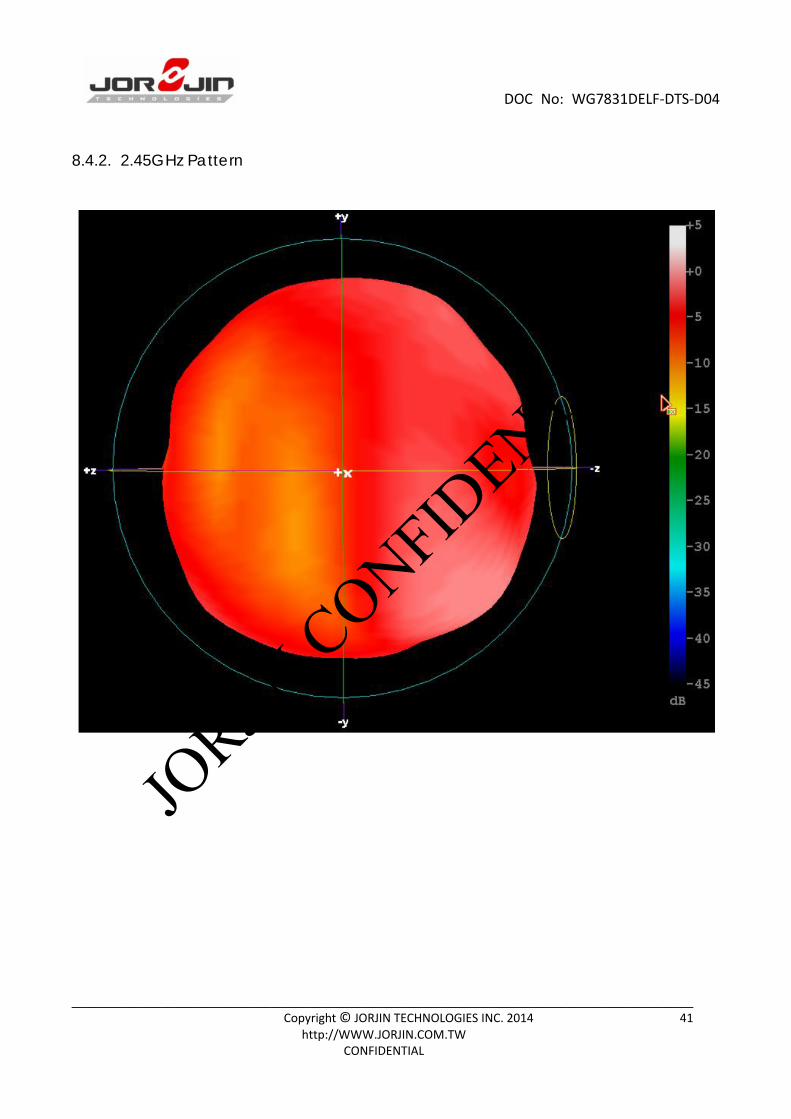
8.4.2. 2.45GHz Pattern
JO
RJIN CONFID
ENTIAL

DOC No: WG7831DELF‐DTS‐D04
____________________________________________________________________________________ Copyright © JORJIN TECHNOLOGIES INC. 2014 42
http://WWW.JORJIN.COM.TW CONFIDENTIAL
8.4.3. 2.5GHz Pattern
JO
RJIN CONFID
ENTIAL

DOC No: WG7831DELF‐DTS‐D04
____________________________________________________________________________________ Copyright © JORJIN TECHNOLOGIES INC. 2014 43
http://WWW.JORJIN.COM.TW CONFIDENTIAL
8.5. Total Efficiency
Frequency ( GHz ) Gain ( dBi ) Total Radiation Efficiency ( % )
2.40 ‐0.34 30
2.41 ‐0.48 29
2.42 ‐0.51 28
2.43 ‐0.14 31
2.44 0.13 33
2.45 0.07 32
2.46 0.49 35
2.47 0.65 35
2.48 0.57 34
2.49 0.46 33
2.50 0.66 34
JORJIN
CONFIDENTIA
L

DOC No: WG7831DELF‐DTS‐D04
____________________________________________________________________________________ Copyright © JORJIN TECHNOLOGIES INC. 2014 44
http://WWW.JORJIN.COM.TW CONFIDENTIAL
9. DESIGN RECOMMENDATIONS
9.1. Design Note on Debug Port
TP1 ,TP2 serve as WLAN and BT debug port, respectively. So test points for these two signals
should be reserved for debugging purpose.
Pin10 (WLAN_IRQ 1V8) needs to be pulled high via 10Kohm and use TP5,TP3 (WL_RS232_RX,
WL_RS232_TX) as hardware interface to communicate with system platform and TI RTTT test
utility for WLAN RF performance test, debug and manufacturing application.
9.2. Module Layout Recommendations
Follow these module layout recommendations:
Digital Signals Layout SDIO signals traces (CMD, D0, D1, D2 and D3) should be routed in parallel to each other
and as short as possible. (Less than 12cm) Besides, every trace length must be the same
as the others.
Enough space above 1.5 time trace width or ground shielding between trace and trace will
be benefit to make sure signal quality, especially for SDIO_CLK _1V8 trace. Remember to
keep them away from the other digital or analog signal traces. Adding ground shielding
around these bus is recommended.
Route trace of SDIO_CLK_1V8 at Top layer without vias. SDIO Clock_1V8, Audio Clock (BT_PCM_AUD_CLK), these digital clock signals are a source
of noise. Keep the traces of these signals as short as possible. Whenever possible, maintain
a clearance around them.
BT_PCM signals should be routed in the same group and it’s better to rout them at the
same layer or confirm them referring to the same reference plane.
Power Trace Power trace for VBAT should be 20mil wide. 1.8V trace should be 15mil wide, at least.
Isolate different power traces with Ground plane. Ground
Having a complete Ground under module for system stable and thermal dissipation.
Move GND vias close to the module of GND pad.
Other Don’t any traces under the module.
For a module with the chip ANT, there should be no metal in this area.
JORJIN
CONFIDENTIA
L

DOC No: WG7831DELF‐DTS‐D04
____________________________________________________________________________________ Copyright © JORJIN TECHNOLOGIES INC. 2014 45
http://WWW.JORJIN.COM.TW CONFIDENTIAL
10. PACKAGE INFORMATION
10.1. Recommended Pad Design
JORJIN
CONFIDENTIA
L

DOC No: WG7831DELF‐DTS‐D04
____________________________________________________________________________________ Copyright © JORJIN TECHNOLOGIES INC. 2014 46
http://WWW.JORJIN.COM.TW CONFIDENTIAL
Note:
1> Pad tolerance as ±30um
2> Unit: mm
JORJIN
CONFIDENTIA
L

DOC No: WG7831DELF‐DTS‐D04
____________________________________________________________________________________ Copyright © JORJIN TECHNOLOGIES INC. 2014 47
http://WWW.JORJIN.COM.TW CONFIDENTIAL
10.2. Module Mechanical Outline
Top and Side View
25±0.2 mm
25.0±0.2 mm
2.5±0.1 mm
JORJIN
CONFIDENTIA
L

DOC No: WG7831DELF‐DTS‐D04
____________________________________________________________________________________ Copyright © JORJIN TECHNOLOGIES INC. 2014 48
http://WWW.JORJIN.COM.TW CONFIDENTIAL
10.3. Ordering Information
Part number: WG7831DELF
10.4. Package Marking
Product number:
WG7831DELF
Date Code: YWW
Y = Digit of the year, ex: 2014=4WW= Week (01~52)
Serial No: ZXXXXXXX
Z Fixed
Serial no XXXXXXX
The series number has a
decimal system
Barcode information:
Serial No. This Sample is “Z0000421”
10 mm
7 mm JO
RJIN CONFID
ENTIAL

DOC No: WG7831DELF‐DTS‐D04
____________________________________________________________________________________ Copyright © JORJIN TECHNOLOGIES INC. 2014 49
http://WWW.JORJIN.COM.TW CONFIDENTIAL
11. SMT AND BAKING RECOMMENDATION
11.1. Baking Recommendation
Baking condition:
- Follow MSL Level 4 to do baking process.
- After bag is opened, devices that will be subjected to reflow solder or other high
temperature process must be
a) Mounted within 72 hours of factory conditions <30°C/60% RH, or
b) Stored at <10% RH.
- Devices require bake, before mounting, if Humidity Indicator Card reads >10%
If baking is required, Devices may be baked for 8 hrs. at 125 °C.
11.2. SMT Recommendation
Recommended Reflow profile:
HJORJIN
CONFIDENTIA
L

DOC No: WG7831DELF‐DTS‐D04
____________________________________________________________________________________ Copyright © JORJIN TECHNOLOGIES INC. 2014 50
http://WWW.JORJIN.COM.TW CONFIDENTIAL
No. Item Temperature (°C) Time (sec)
1 Pre‐heat D1: 140 ~ D2: 200 T1: 80 ~ 120
2 Soldering D2: = 220 T2: 60 +/‐ 10
3 Peak‐Temp. D3: 250 °C max
Note: (1) Reflow soldering is recommended two times maximum.
(2) Add Nitrogen while Reflow process: SMT solder ability will be better.
Stencil thickness: 0.1~ 0.13 mm (Recommended)
Soldering paste (without Pb): Recommended SENJU N705‐GRN3360‐K2‐V can get better
soldering effects.
JORJIN
CONFIDENTIA
L

DOC No: WG7831DELF‐DTS‐D04
____________________________________________________________________________________ Copyright © JORJIN TECHNOLOGIES INC. 2014 51
http://WWW.JORJIN.COM.TW CONFIDENTIAL
12. TPAE REEL INFROMATION
12.1. Cover / Carrier Tape Dimension
1. All dimensions meet EIA‐481 requirements.
2. All dimensions in millimeters unless otherwise stated.
3. Material : Black PS
4. 10 sprocket hole pitch cumulative tolerance +/‐ 0.20mm
5. Carrier camber not to exceed 1mm in 250mm.
6. Packing length for 13” reel : 20.0 Meters.
7. Component packing to 13” reel : 550 pcs.
JORJIN
CONFIDENTIA
L

DOC No: WG7831DELF‐DTS‐D04
____________________________________________________________________________________ Copyright © JORJIN TECHNOLOGIES INC. 2014 52
http://WWW.JORJIN.COM.TW CONFIDENTIAL
13. HISTORY CHANGE
Revision Date Description
D 0.1 2014/01/28 Initial Released
D 0.2 2014/04/08 Update antenna data
D 0.3 2014/05/05 Update the mechanical outline tolerance and package marking.
D 0.4 2014/06/05 Add WLAN transmitter output power note.
JORJIN
CONFIDENTIA
L