
Welcome to PROFIT Pacific-Rim Outlook Forum on IC Technology 1.
40
Welcome to PROFIT Welcome to PROFIT Pacific-Rim Outlook Forum on IC Pacific-Rim Outlook Forum on IC Technology Technology 1
-
date post
21-Dec-2015 -
Category
Documents
-
view
213 -
download
0
Transcript of Welcome to PROFIT Pacific-Rim Outlook Forum on IC Technology 1.
Welcome to PROFITWelcome to PROFIT
Pacific-Rim Outlook Forum on IC TechnologyPacific-Rim Outlook Forum on IC Technology
1
Background of PROFITBackground of PROFIT
IC-DFN International Center for Design on IC-DFN International Center for Design on
Nanotechnologies (2000 – 2005)Nanotechnologies (2000 – 2005)
IC-SOC Giga-Scale System-On-A-Chip IC-SOC Giga-Scale System-On-A-Chip
International Research Center (2006 – 2009)International Research Center (2006 – 2009)
2

IC-SOC and IC-DFN workshops from 2000 to 2008:IC-SOC and IC-DFN workshops from 2000 to 2008: ICDFN 2008 - Tianjin, ChinaICDFN 2008 - Tianjin, China
ICDFN 2007 - Rizhao, ChinaICDFN 2007 - Rizhao, China
ICDFN 2007 - Las Vegas, NVICDFN 2007 - Las Vegas, NV
ICDFN 2006 - Hangzhou, ChinaICDFN 2006 - Hangzhou, China
ICDFN 2006 - Grand Formosa TarokoICDFN 2006 - Grand Formosa Taroko
ICDFN 2005 – ChengduICDFN 2005 – Chengdu
ICDFN 2004 – HawaiiICDFN 2004 – Hawaii
ICDFN 2004 – ChangshaICDFN 2004 – Changsha
ICDFN 2003 – KunmingICDFN 2003 – Kunming
ICDFN 2003 – TaiwanICDFN 2003 – Taiwan
ICDFN 2002 - Santa BabaraICDFN 2002 - Santa Babara
ICDFN 2002 – BeijingICDFN 2002 – Beijing
ICDFN 2002 – TaiwanICDFN 2002 – Taiwan
ICDFN 2001 - TaiwanICDFN 2001 - Taiwan 3
Coping with Vertical Interconnect Coping with Vertical Interconnect BottleneckBottleneck
Jason CongJason CongUCLA Computer Science DepartmentUCLA Computer Science Department
[email protected]://cadlab.cs.ucla.edu/~cong

6
OutlineOutline
Lessons learnedLessons learned
Research challenges and opportunitiesResearch challenges and opportunities

Dr. Mike FritzeDr. Mike Fritze
Chenson Chen and Craig Keast, MIT Lincoln LabsChenson Chen and Craig Keast, MIT Lincoln Labs
“ “Advanced 3D CAD/CAE for the Design of Mixed Signal Systems”, Mr. Kurt Obermiller, PTC Advanced 3D CAD/CAE for the Design of Mixed Signal Systems”, Mr. Kurt Obermiller, PTC
““Technology & Design Infrastructure for High Performance 3D-Ics”, Dr. Albert Young, IBMTechnology & Design Infrastructure for High Performance 3D-Ics”, Dr. Albert Young, IBM
““3D Integrated Circuit with Unlimited Upward Extendibility” Dr. Simon Wong, Stanford University3D Integrated Circuit with Unlimited Upward Extendibility” Dr. Simon Wong, Stanford University
““3D Modular Integration for Massively Stacked Systems” Dr. Volkan Ozguz, Irvine Sensors 3D Modular Integration for Massively Stacked Systems” Dr. Volkan Ozguz, Irvine Sensors
CorporationCorporation
Larry Smith, Sematech Larry Smith, Sematech
CJ Shi, University of WashingtonCJ Shi, University of Washington
Amy Moll, Boise StateAmy Moll, Boise State
Gabriel Loh, Georgia Tech Gabriel Loh, Georgia Tech
Jason Cong, UCLAJason Cong, UCLA
7

Early Studies of 3D ICsEarly Studies of 3D ICs
K. Banerjee, S. J. Souri, P. Kapur, K. C. K. Banerjee, S. J. Souri, P. Kapur, K. C.
Saraswat, “3D ICs: A novel chip design for Saraswat, “3D ICs: A novel chip design for
improving deep submicron interconnect improving deep submicron interconnect
performance and systems-on-chip integration,” performance and systems-on-chip integration,”
Proc. IEEE, Special Issue on Interconnects, May Proc. IEEE, Special Issue on Interconnects, May
2001, pp.602-633.2001, pp.602-633.
Y. Deng, W. Maly, Characteristics of 2.5-D Characteristics of 2.5-D
System Integration Scheme System Integration Scheme
8

9
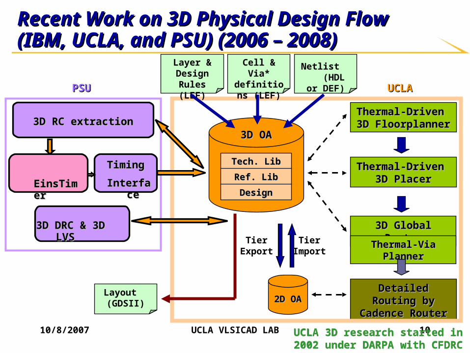
10/8/2007 UCLA VLSICAD LAB 10
Tech. LibTech. Lib
Ref. LibRef. Lib
DesignDesign
3D OA3D OA
Thermal-Driven 3D Thermal-Driven 3D FloorplannerFloorplanner
Thermal-Driven 3D Thermal-Driven 3D PlacerPlacer
3D Global Router3D Global Router
Thermal-Via PlannerThermal-Via PlannerTier Export
Tier Import
Detailed Routing Detailed Routing by Cadence Routerby Cadence Router2D OA2D OA
Recent Work on 3D Physical Design Flow Recent Work on 3D Physical Design Flow (IBM, UCLA, and PSU) (2006 – 2008)(IBM, UCLA, and PSU) (2006 – 2008)
Layer & Design Rules
(LEF)
Cell & Via* definitions
(LEF)
Netlist (HDL or DEF)
3D RC extraction3D RC extraction
Timing Timing
InterfaceInterface
3D DRC & 3D LVS3D DRC & 3D LVS
Layout (GDSII)
EinsTimerEinsTimer
PSUPSU UCLAUCLA
UCLA 3D research started in 2002 under DARPA with CFDRCUCLA 3D research started in 2002 under DARPA with CFDRC
11
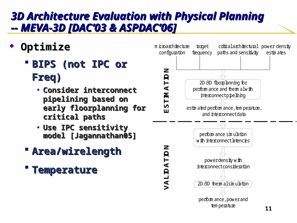
3D Architecture Evaluation with Physical Planning 3D Architecture Evaluation with Physical Planning -- MEVA-3D [DAC’03 & ASPDAC’06]-- MEVA-3D [DAC’03 & ASPDAC’06]
Optimize Optimize
BIPS (not IPC or Freq)BIPS (not IPC or Freq)• Consider interconnect Consider interconnect
pipelining based on early pipelining based on early floorplanning for critical pathsfloorplanning for critical paths
• Use IPC sensitivity model Use IPC sensitivity model [Jagannathan05][Jagannathan05]
Area/wirelength Area/wirelength
TemperatureTemperature
2D/3D floorplanning forperformance and thermal with
interconnect pipelining
performance simulationwith interconnect latencies
2D/3D thermal simulation
microarchitectureconfiguration
targetfrequency
critical architecturalpaths and sensitivity
power densityestimates
estimated performance, temperature,and interconnect data
power density withinterconnect consideration
performance, power andtemperature
ES
TIM
AT
ION
VA
LID
AT
ION
12
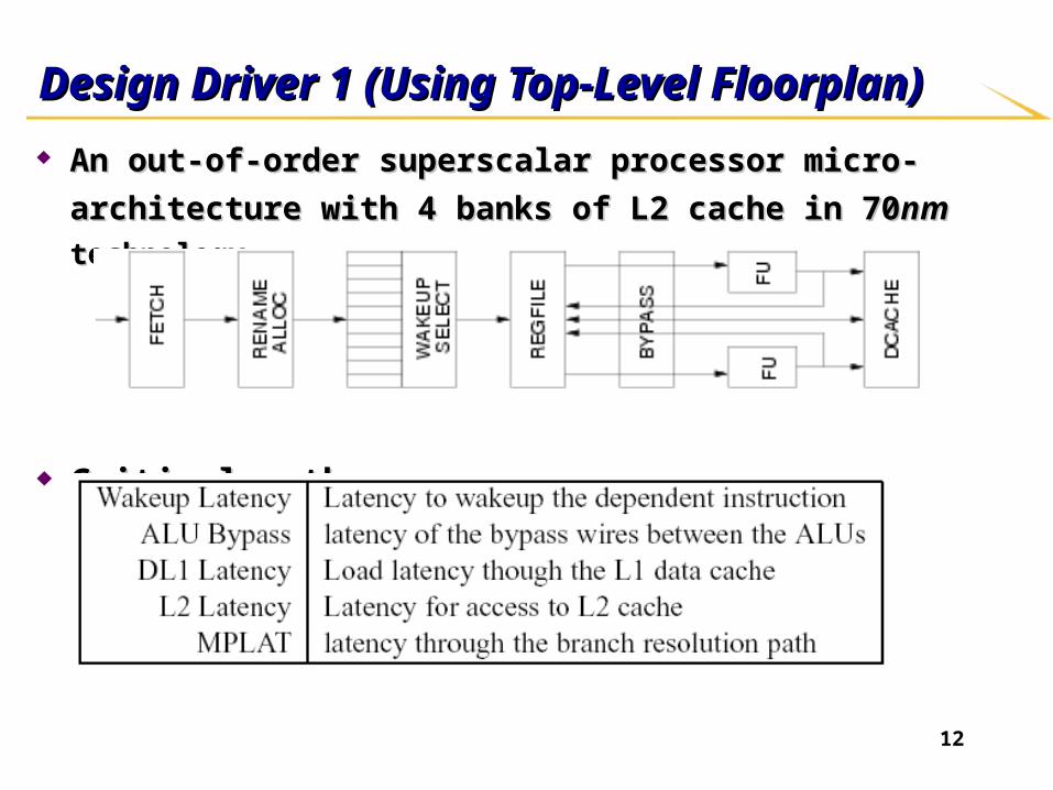
Design Driver 1 (Using Top-Level Floorplan)Design Driver 1 (Using Top-Level Floorplan)
An out-of-order superscalar processor micro-architecture An out-of-order superscalar processor micro-architecture
with 4 banks of L2 cache in 70with 4 banks of L2 cache in 70nm nm technologytechnology
Critical pathsCritical paths

13
Top-Level Wirelength Improvement from 3D Top-Level Wirelength Improvement from 3D StackingStacking
0
20000
40000
60000
80000
100000
120000
3G 4G 5G 6G
2D3D
Assume two device layers
Close to 2X WL reduction (for top-level interconnects)Close to 2X WL reduction (for top-level interconnects)

14
Performance Improvement from 3D Performance Improvement from 3D Stacking Stacking
Assume two device layers
Disappointing ….Disappointing ….

15
2D vs 3D Layout2D vs 3D Layout
2D EV6-like core 3D EV6-like core (2 layers)BIPS= 2.75 BIPS= 2.94
Wakeup loop : The extra cycle is
eliminated.
Branch misprediction resolution loop and the
L2 cache access latency :
Some of the extra cycles are eliminated
Assume two device layers

Design Driver 2 (Using Full RTL)Design Driver 2 (Using Full RTL) An open-source 32-bit processorAn open-source 32-bit processor
Compliant with SPARC V8 architectureCompliant with SPARC V8 architecture
Synthesized by Cadence RTL compiler with UMC 90nm Synthesized by Cadence RTL compiler with UMC 90nm
digital cell library and Faraday memory compilerdigital cell library and Faraday memory compiler Configuration: Single core with 4KB data cache and 4KB Configuration: Single core with 4KB data cache and 4KB
instruction cache as direct-mapped cachesinstruction cache as direct-mapped caches
statistics:statistics:• #cell = 34225#cell = 34225• #macro = 12#macro = 12• #net = 36789#net = 36789• Total area = 6.67 x 10Total area = 6.67 x 1055 μμmm22
UCLA VLSICAD LAB 16

Logical Hierarchy of LEON3Logical Hierarchy of LEON3 LEON3 (77.8% area)LEON3 (77.8% area)
Processor core (11.1% area)Processor core (11.1% area)• Integer unit (6.6% area)Integer unit (6.6% area)• Multiplier (1.6% area)Multiplier (1.6% area)• Divider (0.7% area)Divider (0.7% area)• Memory management unit (2.2% area)Memory management unit (2.2% area)
Register file (16.6% area)Register file (16.6% area) Cache memory (38.1% area)Cache memory (38.1% area) TLB memory (12.0% area)TLB memory (12.0% area)
Debug support unit (13.4% area)Debug support unit (13.4% area)
Other (8.8% area)Other (8.8% area) Memory controller (1.8% area)Memory controller (1.8% area) Interrupt controller (0.3% area)Interrupt controller (0.3% area) UART serial interface (0.7% area)UART serial interface (0.7% area) AMBA AHB bus, AMBA APB bus (4.3% area)AMBA AHB bus, AMBA APB bus (4.3% area) General purpose timer unit (1.4% area)General purpose timer unit (1.4% area) General purpose I/O unit (0.3% area)General purpose I/O unit (0.3% area)
UCLA VLSICAD LAB 17
Other Core
Register file
Cache memory
TLB memory
Debug support
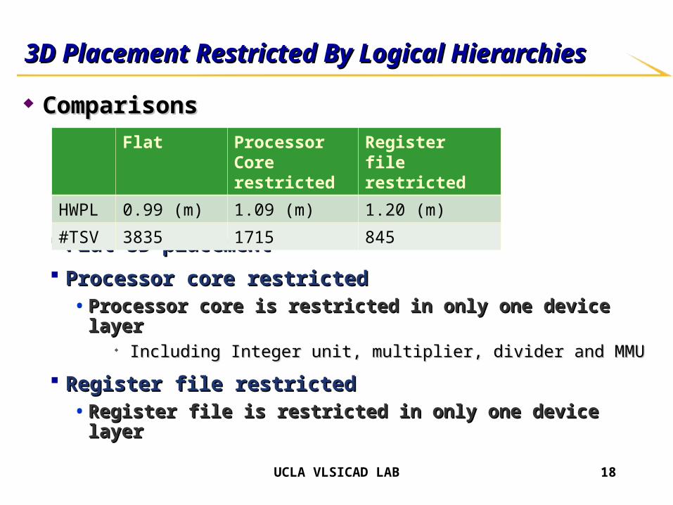
3D Placement Restricted By Logical Hierarchies3D Placement Restricted By Logical Hierarchies
ComparisonsComparisons
Flat 3D placementFlat 3D placement
Processor core restrictedProcessor core restricted• Processor core is restricted in only one device layerProcessor core is restricted in only one device layer
Including Integer unit, multiplier, divider and MMUIncluding Integer unit, multiplier, divider and MMU
Register file restrictedRegister file restricted• Register file is restricted in only one device layerRegister file is restricted in only one device layer
UCLA VLSICAD LAB 18
Flat Processor Core restricted
Register file restricted
HWPL 0.99 (m) 1.09 (m) 1.20 (m)
#TSV 3835 1715 845

19
Lessons LearnedLessons Learned
Block stacking following the logic hierarchy gives Block stacking following the logic hierarchy gives
limited performance and WL reductionlimited performance and WL reduction
Full potential is realized with extensive vertical Full potential is realized with extensive vertical
connectionsconnections

Research challenges and opportunitiesResearch challenges and opportunities
Novel 3D architecture component designs that can cope Novel 3D architecture component designs that can cope
with the vertical interconnect bottleneck,with the vertical interconnect bottleneck,
Physical synthesis tools that can fully comply with Physical synthesis tools that can fully comply with
global and local TSV density constraints,global and local TSV density constraints,
3D microarchitecture exploration, include generating 3D microarchitecture exploration, include generating
optimized 3D physical hierarchies under the TSV density optimized 3D physical hierarchies under the TSV density
constraintsconstraints
New interconnect technologies that can alleviate or New interconnect technologies that can alleviate or
eliminate the vertical interconnect bottleneck.eliminate the vertical interconnect bottleneck.
21
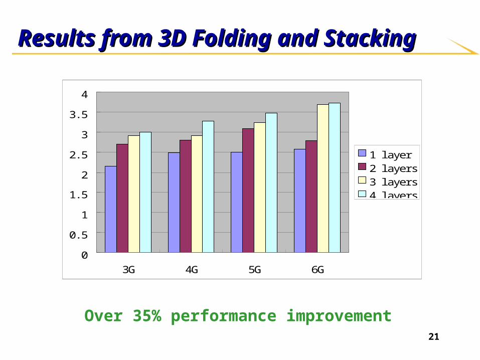
Results from 3D Folding and StackingResults from 3D Folding and Stacking
0
0. 5
1
1. 5
2
2. 5
3
3. 5
4
3G 4G 5G 6G
1 l ayer2 l ayers3 l ayers4 l ayers
Over 35% performance improvement

22
5GHz 3 Device Layer Layout5GHz 3 Device Layer Layout

3D Architectural Blocks – Issue Queue3D Architectural Blocks – Issue Queue Block foldingBlock folding
Fold the entries and place them Fold the entries and place them on different layers on different layers
Effectively shortens the tag linesEffectively shortens the tag lines
Port partitioningPort partitioning Place tag lines and ports on Place tag lines and ports on
multiple layer, thus reducing multiple layer, thus reducing both the height and width of the both the height and width of the ISQ.ISQ.
The reduction in tag and The reduction in tag and matchline wires can help reduce matchline wires can help reduce both power and delay. both power and delay.
Benefits from block foldingBenefits from block folding Maximum delay reduction of Maximum delay reduction of
50%, maximum area 50%, maximum area
reduction of 90% and a reduction of 90% and a
maximum reduction in maximum reduction in
power consumption of 40%power consumption of 40%
(a) 2D issue queue with 4 taglines; (b) block folding; (c) port partitioning

3D Architectural Blocks – Caches3D Architectural Blocks – Caches
Port PartitioningWordline FoldingSingle Layer Design
3D-CACTI: a tool to model 3D cache for area, delay and power3D-CACTI: a tool to model 3D cache for area, delay and power We add port partitioning methodWe add port partitioning method The area impaction of viasThe area impaction of vias
ImprovementsImprovements Port folding performs better than wordline folding for area.(72% vs 51%)Port folding performs better than wordline folding for area.(72% vs 51%) Wordline folding is more effective in reducing the block delay (13% vs 5%)Wordline folding is more effective in reducing the block delay (13% vs 5%) Port folding also performs better in reducing power (13% vs 5%)Port folding also performs better in reducing power (13% vs 5%)
Requires dense TSVsRequires dense TSVs

Research Challenges and Opportunities (2)Research Challenges and Opportunities (2)
Novel 3D architecture component designs that can cope Novel 3D architecture component designs that can cope
with the vertical interconnect bottleneck,with the vertical interconnect bottleneck,
Physical synthesis tools that can fully comply with Physical synthesis tools that can fully comply with
global and local TSV density constraintsglobal and local TSV density constraints
3D microarchitecture exploration, include generating 3D microarchitecture exploration, include generating
optimized 3D physical hierarchies under the TSV density optimized 3D physical hierarchies under the TSV density
constraintsconstraints
New interconnect technologies that can alleviate or New interconnect technologies that can alleviate or
eliminate the vertical interconnect bottleneck.eliminate the vertical interconnect bottleneck.

Current Approaches to Handling TSV Constraints
Approach 1: minimizing
WL + k* #TSVs
Approach 2: minimizing WL (or weighted WL)
subject to the total #TSV constraints
None of these can handle local TSV density
constraints

Research Challenges and Opportunities (3)Research Challenges and Opportunities (3)
Novel 3D architecture component designs that can cope Novel 3D architecture component designs that can cope
with the vertical interconnect bottleneck,with the vertical interconnect bottleneck,
Physical synthesis tools that can fully comply with Physical synthesis tools that can fully comply with
global and local TSV density constraintsglobal and local TSV density constraints
3D microarchitecture exploration, include generating 3D microarchitecture exploration, include generating
optimized 3D physical hierarchies under the TSV density optimized 3D physical hierarchies under the TSV density
constraintsconstraints
New interconnect technologies that can alleviate or New interconnect technologies that can alleviate or
eliminate the vertical interconnect bottleneck.eliminate the vertical interconnect bottleneck.
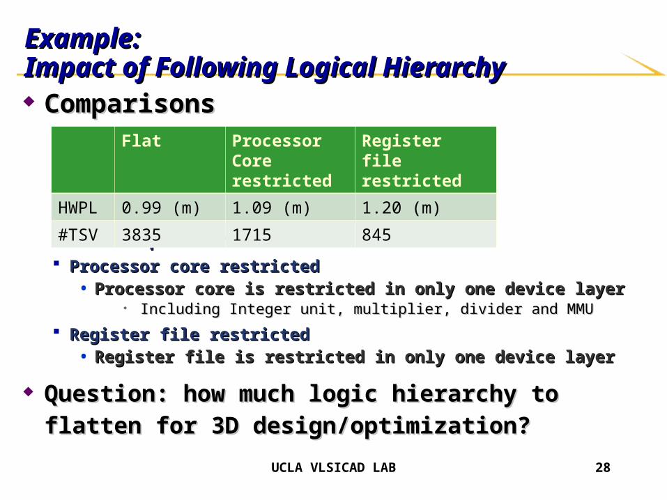
Example: Example: Impact of Following Logical HierarchyImpact of Following Logical Hierarchy ComparisonsComparisons
Flat 3D placementFlat 3D placement
Processor core restrictedProcessor core restricted• Processor core is restricted in only one device layerProcessor core is restricted in only one device layer
Including Integer unit, multiplier, divider and MMUIncluding Integer unit, multiplier, divider and MMU
Register file restrictedRegister file restricted• Register file is restricted in only one device layerRegister file is restricted in only one device layer
Question: how much logic hierarchy to flatten for 3D Question: how much logic hierarchy to flatten for 3D
design/optimization?design/optimization?
UCLA VLSICAD LAB 28
Flat Processor Core restricted
Register file restricted
HWPL 0.99 (m) 1.09 (m) 1.20 (m)
#TSV 3835 1715 845

Research Challenges and Opportunities (4)Research Challenges and Opportunities (4)
Novel 3D architecture component designs that can cope Novel 3D architecture component designs that can cope
with the vertical interconnect bottleneck,with the vertical interconnect bottleneck,
Physical synthesis tools that can fully comply with Physical synthesis tools that can fully comply with
global and local TSV density constraintsglobal and local TSV density constraints
3D microarchitecture exploration, include generating 3D microarchitecture exploration, include generating
optimized 3D physical hierarchies under the TSV density optimized 3D physical hierarchies under the TSV density
constraintsconstraints
New interconnect technologies that can alleviate or New interconnect technologies that can alleviate or
eliminate the vertical interconnect bottleneckeliminate the vertical interconnect bottleneck..

Contactless Interconnects
TX
RX
M fieldTX
RXE field
Inductor-coupled Interconnect
Capacitor-coupled Interconnect
Advantages:Advantages:More effective for longer distance communication (hundreds of microns)
Disadvantages:Disadvantages: Larger size Higher cross talks between channels
Advantages:Advantages:Smaller sizeLower cross talk
Disadvantages:Disadvantages:Effective for short distance communication (several microns)
Suitable for 3DIC integration

Die Photos (MIT LL 0.18um)
Coupling Capacitor
TX in Layer 2
RX in Layer 1
Coupling Capacitor
TX in Layer 2
RX in Layer 1
BISI die photo RFI die photo

BISI Test Results [ISSCC’07]
Data rate:10Gbps
Output Eye diagram Output versus Input
Input
Output
20ps/div
50mV/div
500ps/div

33
ConclusionsConclusions
Never enough for vertical interconnects (VIs)Never enough for vertical interconnects (VIs)
Need to cope with VI constraintsNeed to cope with VI constraints Novel 3D architecture component designs Novel 3D architecture component designs
Physical synthesis tools that can fully comply with global and Physical synthesis tools that can fully comply with global and local TSV density constraints,local TSV density constraints,
3D microarchitecture exploration, include generating optimized 3D microarchitecture exploration, include generating optimized 3D physical hierarchies under the TSV density constraints3D physical hierarchies under the TSV density constraints
Need to find ways to break VI bottleneckNeed to find ways to break VI bottleneck New interconnect technologiesNew interconnect technologies
Acknowledgements
We would like to thank the supports from
DARPA
Support from the primary contractors --
Collaboration with CFDRC and IBM
Publications are available from
http://cadlab.cs.ucla.edu/~cong

35
Example 1 Processor ParametersExample 1 Processor Parameters

Example 2 Flat 3D PlacementExample 2 Flat 3D Placement
UCLA VLSICAD LAB 36
Other Core
Register file
Cache memory
TLB memory
Debug support
HPWL = 0.99 (m)HPWL = 0.99 (m)
#TSV = 3835#TSV = 3835
Placement (bottom layer, top layer)Placement (bottom layer, top layer)

Example 2 Processor Core RestrictedExample 2 Processor Core Restricted
HPWL = 1.09 (m)HPWL = 1.09 (m)
#TSV = 1715#TSV = 1715
Placement (bottom, top)Placement (bottom, top)
UCLA VLSICAD LAB 37
Other Core
Register file
Cache memory
TLB memory
Debug support
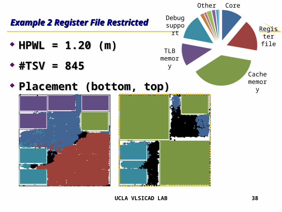
Example 2 Register File RestrictedExample 2 Register File Restricted
HPWL = 1.20 (m)HPWL = 1.20 (m)
#TSV = 845#TSV = 845
Placement (bottom, top)Placement (bottom, top)
UCLA VLSICAD LAB 38
Other Core
Register file
Cache memory
TLB memory
Debug support

Further Discussions of Example 2Further Discussions of Example 2 ComparisonsComparisons
To quantify the impact of TSVTo quantify the impact of TSV• Example: TSV in MIT Lincoln 180nm SOI 3D technologyExample: TSV in MIT Lincoln 180nm SOI 3D technology
Resistance: one TSV is equivalent to a 8-20 Resistance: one TSV is equivalent to a 8-20 μμm metal 2 wirem metal 2 wire Capacitance: one TSV is equivalent to a 0.2Capacitance: one TSV is equivalent to a 0.2 μ μm metal 2 wirem metal 2 wire
ConclusionConclusion TSV impact on the RC is not significantTSV impact on the RC is not significant Some logical units are preferred to be distributed on different Some logical units are preferred to be distributed on different
device layersdevice layers• E.g., the register file in the LEON3 circuitE.g., the register file in the LEON3 circuit
Flat 3D placement is preferred to optimize total RCFlat 3D placement is preferred to optimize total RCUCLA VLSICAD LAB 39
Flat Processor Core restricted
Register file restricted
HWPL 0.99 (m) 1.09 (m) 1.20 (m)
#TSV 3835 1715 845

3D Capacitive RF-Interconnect
NRZ baseband signal is up-converted by an RF carrier at the transmitter (tier N+1) using ASK (Amplitude-Shift-Key) modulation; and an RF envelope detector at the receiver (tier N) recovers NRZ data in the receiver.
Transmitter
Receiver
Tier N+1
Tier N
Buffer
BufferEnvelope Detector Sense Amp
Coupling Capacitor
ASK ModulatorASK Signal INPUT
OUTPUT