Week2 Diodes Transistors - University of California, …...Diode 2 One can think of a diode as a...
27
Diode Transistor Physics 120/220 Prof. Anyes Taffard
Transcript of Week2 Diodes Transistors - University of California, …...Diode 2 One can think of a diode as a...

DiodeTransistor
Physics 120/220
Prof. Anyes Taffard
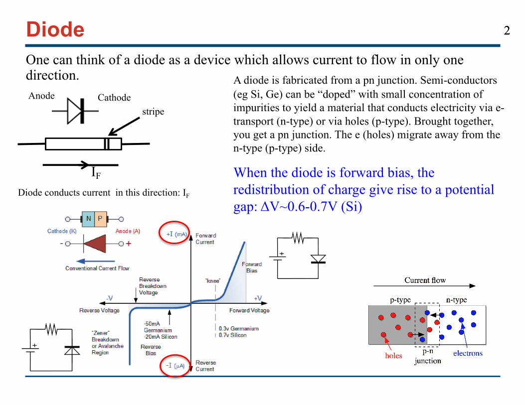
22DiodeOne can think of a diode as a device which allows current to flow in only one direction.
Anode Cathode
stripe
Diode conducts current in this direction: IF
IF
A diode is fabricated from a pn junction. Semi-conductors (eg Si, Ge) can be “doped” with small concentration of impurities to yield a material that conducts electricity via e-transport (n-type) or via holes (p-type). Brought together, you get a pn junction. The e (holes) migrate away from the n-type (p-type) side.
When the diode is forward bias, the redistribution of charge give rise to a potential gap: ΔV~0.6-0.7V (Si)
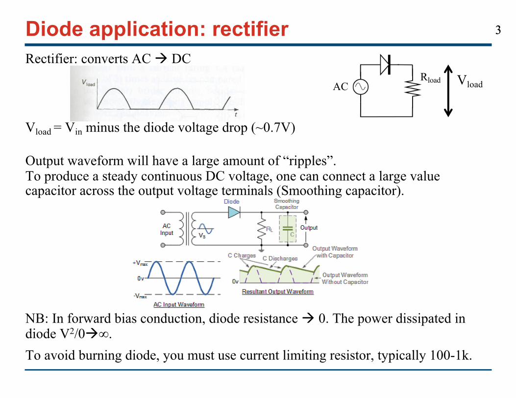
33Diode application: rectifierRectifier: converts AC à DC
Vload = Vin minus the diode voltage drop (~0.7V)
Output waveform will have a large amount of “ripples”.
To produce a steady continuous DC voltage, one can connect a large value
capacitor across the output voltage terminals (Smoothing capacitor).
NB: In forward bias conduction, diode resistance à 0. The power dissipated in
diode V2/0à∞.
To avoid burning diode, you must use current limiting resistor, typically 100-1k.
RloadAC
Vload

44Diode application: Full wave bridge rectifierAnother example: Full wave bridge rectifier
The current through the load flows always in the same direction.During each ½ cycle, the current flows through 2 diodes, so the output voltage drops by 2�0.7=1.4V with respect to the input voltage.
Positive 1/2 cycle. D1 & D2 conduct in seriesD3 and D4 are reverse biased
Negative 1/2 cycle. D3 & D4 conduct in seriesD1 and D2 are reverse biased

55Diode application: LimiterThis circuit limits the output “swing” to one diode drop (~�0.6-0.7V)This clamp circuit is often used as input protection for a high gain amplifier. • For eg, RHS diode at +5V, Vout is clamped at about +0.6V and -0.6V.
NB: If you burn a diode, you would not see it beside the fact that your circuit isn't working so well. Use a tester (diode setting) to check your diode.

6
Transistors & Transistor circuits

77IntroductionOne of the most important example of “active” component:• a device that can amplify: produce an output signal with more power than the input. The additional power comes from an external source of power (PS).
Transistor is the essential ingredient of every electronic circuit:• amplifier• switch• logic gates/digital computer (eg CPU contains >4 billions transistors)
Integrated circuits (ICs) have largely replaced circuits constructed with discrete transistors.ü Transistors count on ICs: x2/year (Moore’s law)
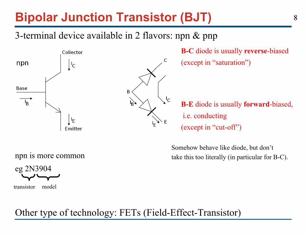
88Bipolar Junction Transistor (BJT)3-terminal device available in 2 flavors: npn & pnp
npn is more commoneg 2N3904
Other type of technology: FETs (Field-Effect-Transistor)
B-C diode is usually reverse-biased(except in “saturation”)
B-E diode is usually forward-biased,i.e. conducting(except in “cut-off”)
transistor model
Somehow behave like diode, but don’t take this too literally (in particular for B-C).
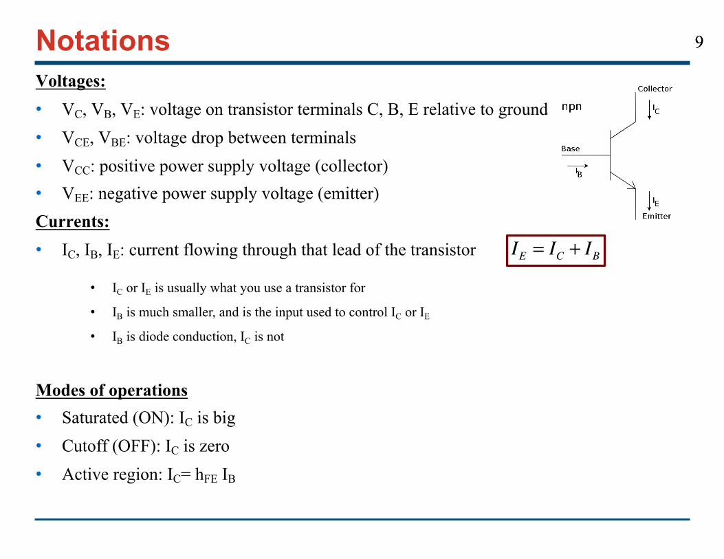
99NotationsVoltages:• VC, VB, VE: voltage on transistor terminals C, B, E relative to ground• VCE, VBE: voltage drop between terminals• VCC: positive power supply voltage (collector)• VEE: negative power supply voltage (emitter)Currents:• IC, IB, IE: current flowing through that lead of the transistor
Modes of operations• Saturated (ON): IC is big• Cutoff (OFF): IC is zero• Active region: IC= hFE IB
• IC or IE is usually what you use a transistor for
• IB is much smaller, and is the input used to control IC or IE
• IB is diode conduction, IC is not
IE = IC + IB
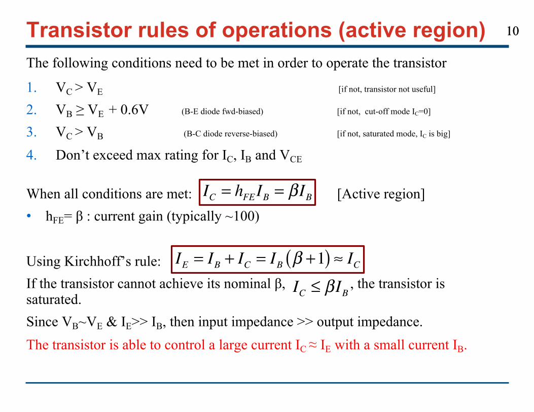
1010Transistor rules of operations (active region)The following conditions need to be met in order to operate the transistor
1. VC > VE [if not, transistor not useful]
2. VB ≥ VE + 0.6V (B-E diode fwd-biased) [if not, cut-off mode IC=0]
3. VC > VB (B-C diode reverse-biased) [if not, saturated mode, IC is big]
4. Don’t exceed max rating for IC, IB and VCE
When all conditions are met: [Active region]
• hFE= β : current gain (typically ~100)
Using Kirchhoff’s rule:
If the transistor cannot achieve its nominal β, , the transistor is saturated.
Since VB~VE & IE>> IB, then input impedance >> output impedance.
The transistor is able to control a large current IC ≈ IE with a small current IB.
IC = hFEIB = β IB
IE = IB + IC = IB β +1( ) ≈ ICIC ≤ β IB

1111ExampleGiven VCC=20V, VB=5.6V.R1=4.7k, R2= 3.3k and hFE=100.Find VE, IE, IB
VE =VB − 0.6 = 5V
IE =VE − 0R2
= 53.3k
=1.5mA
IB =IE
1+ hFE( ) =1.5100
= 0.015mA
IC = IE − IB ≈ IE =1.5mA
VC =VCC − ICR1= 20−1.5mA × 4.7k≈ 20− 7 =13V
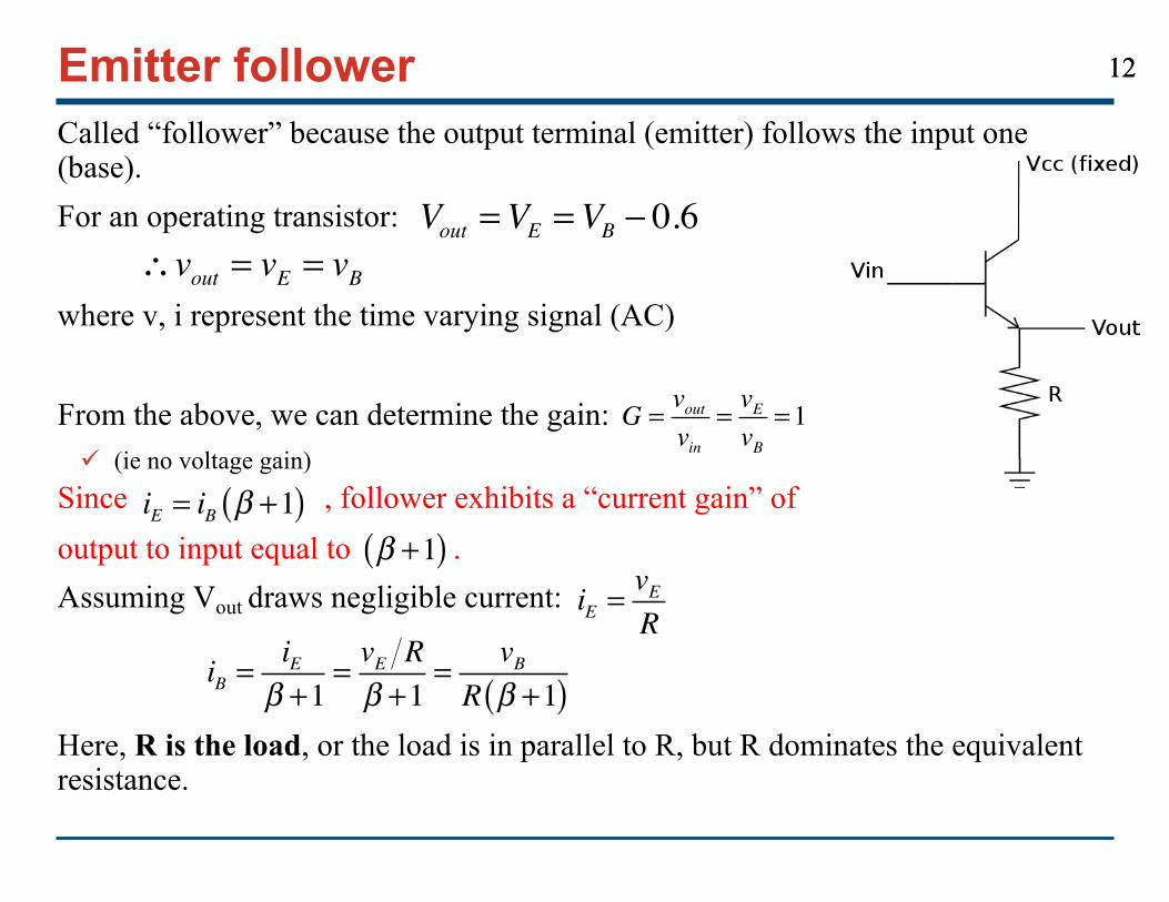
1212Emitter followerCalled “follower” because the output terminal (emitter) follows the input one (base).For an operating transistor:
where v, i represent the time varying signal (AC)
From the above, we can determine the gain:ü (ie no voltage gain)
Since , follower exhibits a “current gain” ofoutput to input equal to .Assuming Vout draws negligible current:
Here, R is the load, or the load is in parallel to R, but R dominates the equivalent resistance.
Vout =VE =VB − 0.6∴vout = vE = vB
G = voutvin
= vEvB
=1
iE = iB β +1( )β +1( )
iE =vER
iB =iE
β +1= vE Rβ +1
= vBR β +1( )

1313Emitter follower input/output impedanceInput impedance of the follower (@base):
Output impedance (@ emitter):
where Zsource is the impedance of the circuit which gave rise to vin.
The emitter-follower reduces the output impedance relative to that of the source impedance by a factor (β+1)~100.
This configuration is useful for impedance matching applications, because of the very high input impedance while having a relatively low output impedance.
Zin =viniin
= vBiB
= Zload β +1( )
Zout =viniE
= vinβ +1( )iB
= Zsource
β +1( )
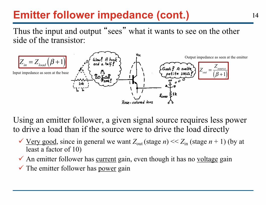
1414Emitter follower impedance (cont.)Thus the input and output �sees� what it wants to see on the other side of the transistor:
Using an emitter follower, a given signal source requires less power to drive a load than if the source were to drive the load directlyü Very good, since in general we want Zout (stage n) << Zin (stage n + 1) (by at
least a factor of 10)ü An emitter follower has current gain, even though it has no voltage gainü The emitter follower has power gain
Zout =Zsourceβ +1( )
Zin = Zload β +1( ) Output impedance as seen at the emitter
Input impedance as seen at the base

-2€ : input impedance of Emitter - follower Using voltage divider approach to measure Zion
1- - - - -
t signals,
Vcc , • win we 'll use Vppi t i '
i''
Esu. no.¥÷z.vn/IcaeauasezIs
,3
T'
I 1-Ninfa;§e I 3 Zin'
43 I I L , re - arrangeto entreat Zin
I I=
I { the '
'- - - - - i
zin Zin -
-Zs I
=L Nin - VB
Zin -
-
UI→ Recall : voltage drop across Z is proportional
is .,f!µ,,) tin = RE ( Ptt) to ratio of impedances .
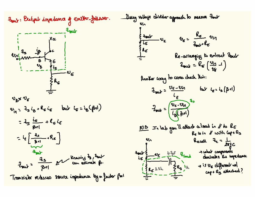
Zoar : Output impedance ofEmitter - follower . Using voltage divider approach ho measure tour
winO
,- - - - - - - - - -
four
I
, Vcc Estado ,= be =€ Vin
( tie Zoeett RE
"Is sirs
doc
/ } RE
Ninny;§e , =L Re - arranging to extract Four
I I
'-
. -II-
Iie. -
itout -
- RE (
Y- I )
✓ NE
{ theAnother way
to crosscheck this :
Zoey =VEIN but ie -
- is ( BH )
Up #VEEE
Win -
-tsi ,ztREiE but iE=iBCpH) font
=UE-V↳
IBLBH )= Is t REIE
Btl NI In lab you'll attach ahead in Kb RE
Re is in k with Capt Rz= ie [ Y÷ t RE )
covin
Recall Zc --
gutgcin I
tout tout } 4.7µF → what components
µknowing tis ,
tout ieTIE- -
-Goad dominates the impedance
can estimate p -
' F)IT I
tout ' 2¥ 13µg.sn { R,
inhis UE differential
' - - -- - -
-t -
'
Capt Rz attached ?
Transistor reduces source impedance byafachrpnt I ta-
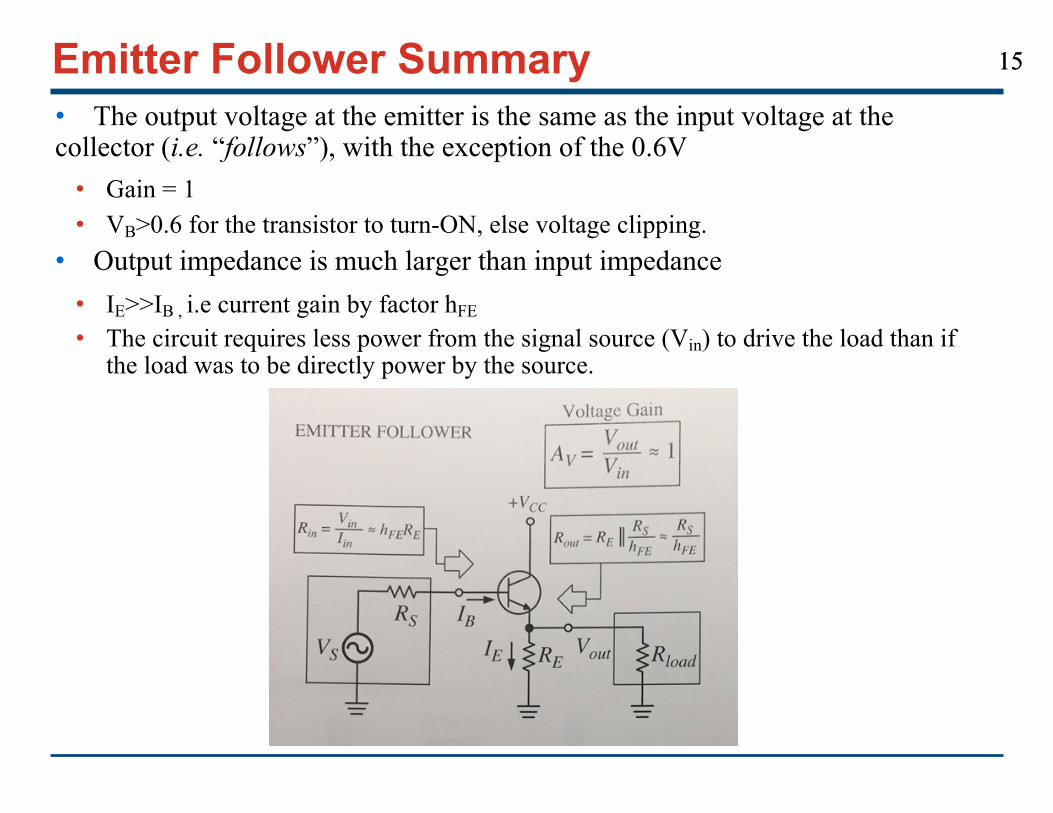
1515Emitter Follower Summary• The output voltage at the emitter is the same as the input voltage at the collector (i.e. “follows”), with the exception of the 0.6V• Gain = 1• VB>0.6 for the transistor to turn-ON, else voltage clipping.• Output impedance is much larger than input impedance• IE>>IB , i.e current gain by factor hFE
• The circuit requires less power from the signal source (Vin) to drive the load than if the load was to be directly power by the source.
1616
Determining the AC signal gain:
Collector resistor: (1) [Ohm’s law]
Emitter: (2) [Ohm’s law]
Transistor: (3) [Active region]
Node @ output
(4)
From (1) or
From (3) (using (2))
(using (4))
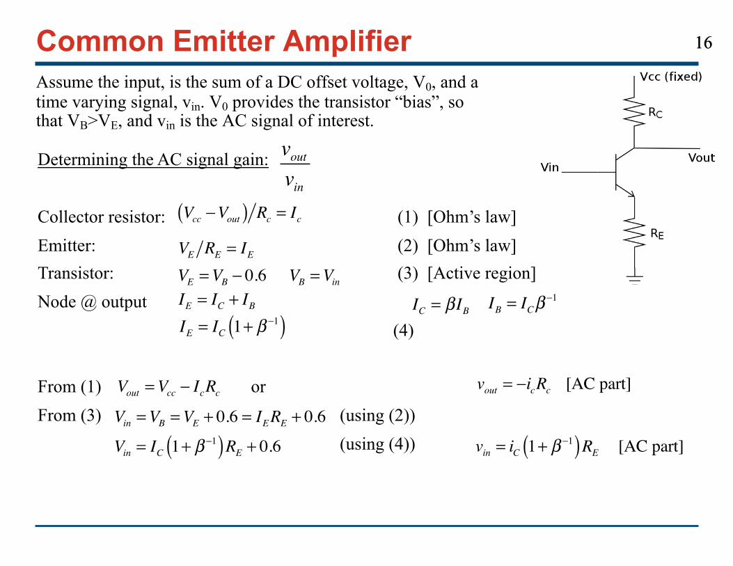
Common Emitter AmplifierAssume the input, is the sum of a DC offset voltage, V0, and a
time varying signal, vin. V0 provides the transistor “bias”, so
that VB>VE, and vin is the AC signal of interest.
voutvin
Vcc −Vout( ) Rc = IcVE RE = IEVE =VB − 0.6 VB =VinIE = IC + IBIE = IC 1+ β −1( )
IC = β IB IB = ICβ−1
Vout =Vcc − IcRc vout = −icRc [AC part]
Vin =VB =VE + 0.6 = IERE + 0.6
Vin = IC 1+ β −1( )RE + 0.6 vin = iC 1+ β −1( )RE [AC part]

1717Common Emitter Amplifier (cont.)
Gain: β ~ 100 ∴ β −1 ~ 0.01
AC gain of common emitter amplifier
Note gain <0 à inverting amplifier + à -
!"#$!%&
= −)*+*)* 1 + ./0 +1
23 = −+4+1
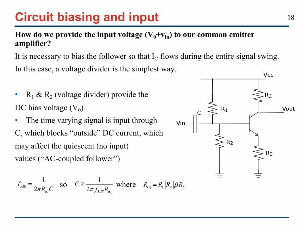
1818Circuit biasing and inputHow do we provide the input voltage (V0+vin) to our common emitter amplifier?It is necessary to bias the follower so that IC flows during the entire signal swing.In this case, a voltage divider is the simplest way.
• R1 & R2 (voltage divider) provide theDC bias voltage (V0)• The time varying signal is input throughC, which blocks “outside” DC current, which may affect the quiescent (no input) values (“AC-coupled follower”)
so whereCRf
eqdB3 2
1p
=eq32
1Rf
CdBp
³ ERRRR b21eq =
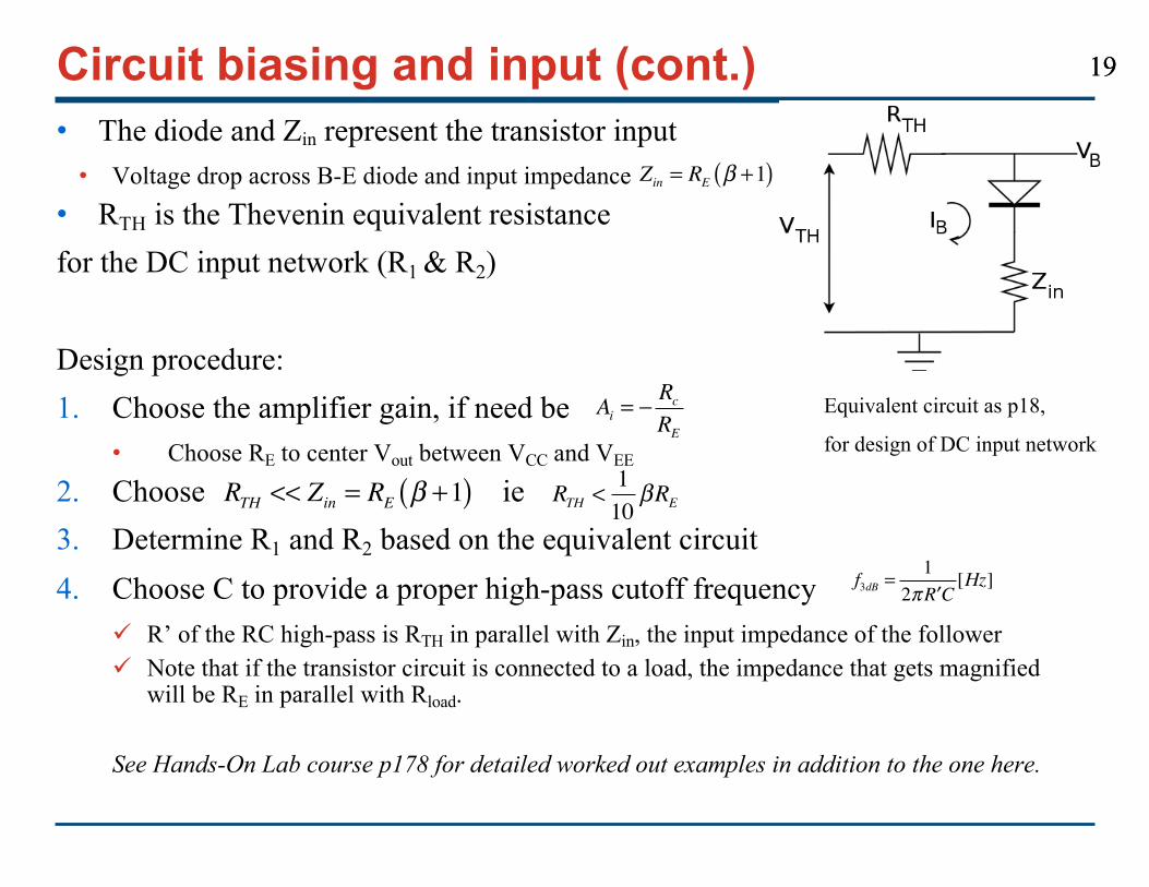
1919Circuit biasing and input (cont.)• The diode and Zin represent the transistor input
• Voltage drop across B-E diode and input impedance
• RTH is the Thevenin equivalent resistance
for the DC input network (R1 & R2)
Design procedure:
1. Choose the amplifier gain, if need be
• Choose RE to center Vout between VCC and VEE
2. Choose ie
3. Determine R1 and R2 based on the equivalent circuit
4. Choose C to provide a proper high-pass cutoff frequency
ü R’ of the RC high-pass is RTH in parallel with Zin, the input impedance of the follower
ü Note that if the transistor circuit is connected to a load, the impedance that gets magnified
will be RE in parallel with Rload.
See Hands-On Lab course p178 for detailed worked out examples in addition to the one here.
Equivalent circuit as p18,
for design of DC input network
Zin = RE β +1( )
RTH << Zin = RE β +1( ) RTH < 110
βRE
Ai = − RcRE
f3dB =1
2π ′R C[Hz]

2020Common Emitter Follower Amplifier Summary• Current gain, but no voltage gain• Avoid clipping during negative input swings• Voltage divider (R1 & R2) is used to give the input signal (after passing through the cap) a positive DC level or operating point (also known as quiescent point)• Both input and output caps are added so that an AC input/output signal can be added without disturbing the DC operating point. Caps act as filters.
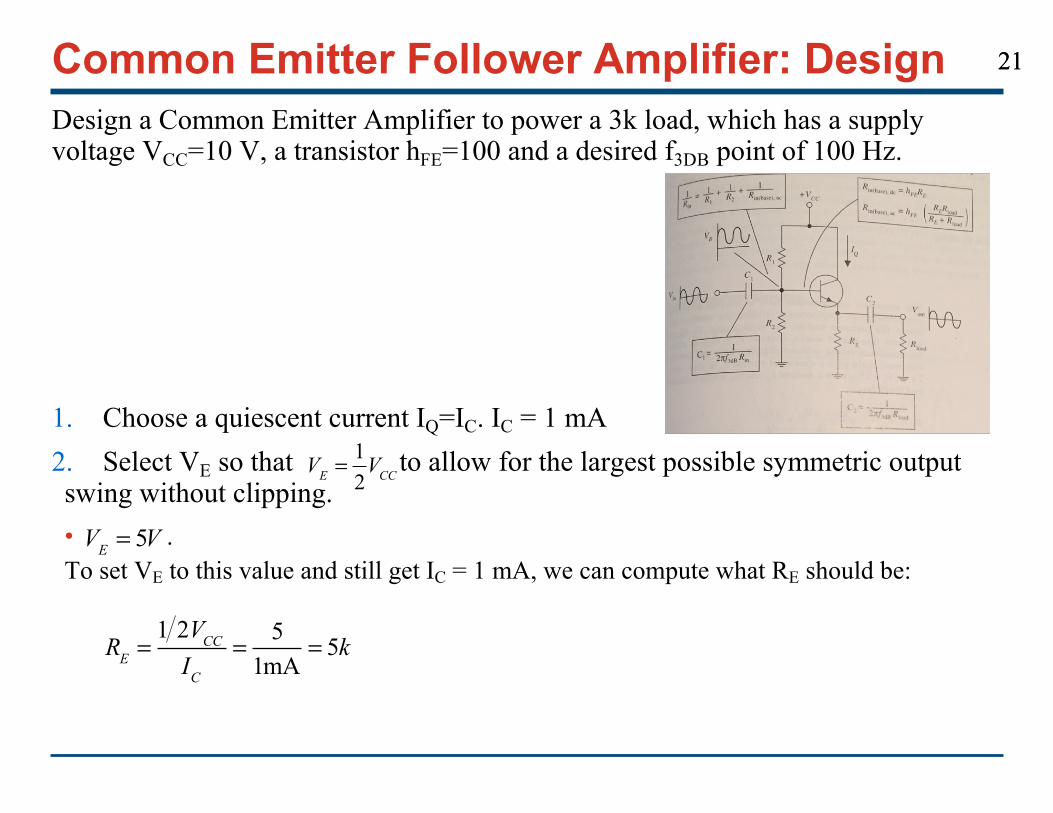
2121Common Emitter Follower Amplifier: DesignDesign a Common Emitter Amplifier to power a 3k load, which has a supply voltage VCC=10 V, a transistor hFE=100 and a desired f3DB point of 100 Hz.
1. Choose a quiescent current IQ=IC. IC = 1 mA2. Select VE so that to allow for the largest possible symmetric output swing without clipping. • . To set VE to this value and still get IC = 1 mA, we can compute what RE should be:
VE =12VCC
VE = 5V
RE =1 2VCCIC
= 51mA
= 5k

2222Common Emitter Follower Amplifier: Design (cont.)
3. Set for quiescent conditions (to match up VE so as to avoid clipping)
• To set VB we use the voltage divider. The ratio between R1 & R2 is determined by rearranging the voltage-divider relation and substitution into it VB.
• We can make an approximation and set R1=R2. • This “forgets” the 0.6 V drop, which usually isn’t too dramatic.• The actual size of R1 & R2 should be such that their parallel resistance is less or equal to
1/10 the DC (quiescent) input resistance at the base. This prevents the voltage divider from lowering under loading conditions:
• Here
• Thus R1=R2=100k
VB =VE + 0.6
R2R1
=VB
VCC −VB=
VE + 0.6VCC − VE + 0.6( )
R1R2
R1 + R2
≤ 110Rin(base),DC
R2≤ 1
10Rin(base),DC (using the approx R=R1=R2 )
Rin(base),DC = hFERE =100×5k = 500k
Here we don’t need to worry about the AC coupled load.
It does not influence the voltage divider because we assume the quiescent setup conditions.
C2 acts as an open circuit, thus “eliminating” the presence of the load

2323Common Emitter Follower Amplifier: Design (cont.)
4. Finally we need to choose the AC coupling capacitor, C1, so that to block out the DC levels and other undesired frequencies.
• C1 forms a high-pass filter with Rin. To find Rin, we treat the voltage divider and Rin(base), AC as being in parallel:
• We must treat RE and Rload in parallel and multiply by hFE to find Rin(base), AC
• Let’s find Rin:
• Now we can choose C1 to set the f3DB point (C1 and Rin form a high-pass filter):
• C2 forms a high-pass filter with the load:
1Rin
= 1R1
+ 1R2
+ 1Rin(base),AC
No longer treat the load as being absent when fluctuating signals are applied to the input. The capacitor begins to pass a displacement current.
Rin(base),AC = hFERERloadRE + Rload
⎛
⎝⎜⎞
⎠⎟=100 5k × 3k
5k + 3k⎛⎝⎜
⎞⎠⎟=190k
1Rin
= 1100k
+ 1100k
+ 1190
⇒ Rin = 40k
C1 =1
2π f3DBRin= 12π ×100× 40k
= 0.04µF
C2 =1
2π f3DBRload= 12π ×100× 3k
= 0.5µF

24
Backup
2525
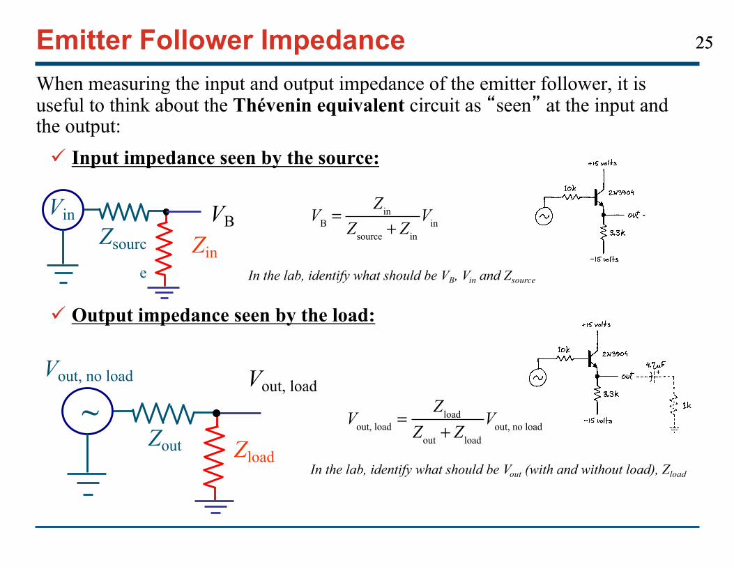
When measuring the input and output impedance of the emitter follower, it is useful to think about the Thévenin equivalent circuit as �seen� at the input and the output:ü Input impedance seen by the source:
ü Output impedance seen by the load:
Emitter Follower Impedance
~Zout Zload
Vout, loadVout, no load
VinZsourc
eZin
VB VB =Zin
Zsource + ZinVin
Vout, load =Zload
Zout + Zload
Vout, no load
In the lab, identify what should be VB, Vin and Zsource
In the lab, identify what should be Vout (with and without load), Zload