Wafer-Level Packaging (WLP) and its Applications ... · Pb-free solder balls are used as die to ......
8
Click here for an overview of the wireless components used in a typical radio transceiver. Keywords: WLP, SMT, PCB design, wafer level package, tape and reel, T&R APPLICATION NOTE 1891 WAFER-LEVEL PACKAGING (WLP) AND ITS APPLICATIONS Abstract: This application note discusses Maxim Integrated’s wafer-level package (WLP) and provides the PCB design and SMT assembly guidelines for the WLP. Introduction The wafer-level package (WLP) offers advantages of small size and low inductance. Maxim Integrated's WLP are manufactured on wafers. Backside lamination is applied to enhance the mechanical strength of WLP body. Pb-free solder balls are used as die to PCB interconnects. An example package outline is showing in Figure 1. Page 1 of 8
Transcript of Wafer-Level Packaging (WLP) and its Applications ... · Pb-free solder balls are used as die to ......
Click here for an overview of the wireless components used in a typical radio transceiver.
Keywords: WLP, SMT, PCB design, wafer level package, tape and reel, T&R
APPLICATION NOTE 1891
WAFER-LEVEL PACKAGING (WLP) AND ITS APPLICATIONS
Abstract: This application note discusses Maxim Integrated’s wafer-level package (WLP) and provides the PCB design and SMT assembly guidelines for the WLP.
IntroductionThe wafer-level package (WLP) offers advantages of small size and low inductance. Maxim Integrated's WLP are manufactured on wafers. Backside lamination is applied to enhance the mechanical strength of WLP body. Pb-free solder balls are used as die to PCB interconnects. An example package outline is showing in Figure 1.
Page 1 of 8

Figure 1. SEM photo of a WLP.Maxim Integrated ships WLPs in tape-and-reel (T&R) format. Tape-and -reel requirements are based on the EIA-481 standard.Additional T&R information ›
Page 2 of 8
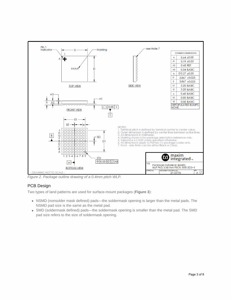
Figure 2. Package outline drawing of a 0.4mm pitch WLP.
PCB DesignTwo types of land patterns are used for surface-mount packages (Figure 3):
NSMD (nonsolder mask defined) pads—the soldermask opening is larger than the metal pads. The NSMD pad size is the same as the metal pad.SMD (soldermask defined) pads—the soldermask opening is smaller than the metal pad. The SMD pad size refers to the size of soldermask opening.
Page 3 of 8

Figure 3. Illustration of NSMD and SMD land pad patterns.
Although both NSMD and SMD pads are used in applications, NSMD pads are recommended. NSMD pads have the advantages of more precise pad dimension and better solder joint reliability at board side. Only one type of a pad (NSMD or SMD) and one type of pad surface finish should be used at a given footprint. The recommended pad sizes are listed in Table 1. The width of the trace at entry to an NSMD pad should be no more than 100µm to avoid excessive wetting of solder onto the trace, which can change the solder joint shape. A teardrop is recommended at the trace entry to lower the risk of trace crack.
When wide trace entry to a pad is required for reasons such as high current carrying, SMD pads can be used. Larger metal pads and wider metal traces can be used for SMD pads.
Via in pad (VIP) is acceptable. The dimple at VIP can cause solder voiding at assembly. Small voids at VIP do not significantly degrade the solder joint reliability. The user is suggested to assess the acceptable via quality. Complete flat VIP can be achieved with via capping although it is not required. It is recommended to put VIP at corner ball location to improve the PCB reliability.
Table 1. Recommended NSMD Pad Designs
Ball Pitch(mm)
Acceptable PCB Pad Diameter (µm)
Recommended PCB Pad Diameter (µm)
0.5 220 to 280 250
0.4 200 to 260 250
0.35 190 to 220 200
0.3 160 to 190 180
Page 4 of 8
PCB Surface FinishOSP (Organic Solderability Preservative), ENIG (Electroless Nickel/Immersion Gold), ElectrolyticNickel/Gold, ENEPIG (Electroless Nickel Electroless Palladium/Immersion Gold), Immersion Silver and Immersion Tin finishes are used in the industry. OSP is recommended for applications that require drop test reliability.
SMT AssemblyStandard SMT equipment and process are used for WLP assembly. The process flow is the following:
Incoming WLP inspection
Paste deposition
WLP pick and placement
Solder reflow
Flux cleaning (optional)
Inspection
Both solder paste or flux printing and flux dipping approaches provide acceptable assembly quality and reliability. Maxim Integrated WLP meet JEDEC level 1 moisture sensitivity classification. No baking is needed before assembly.
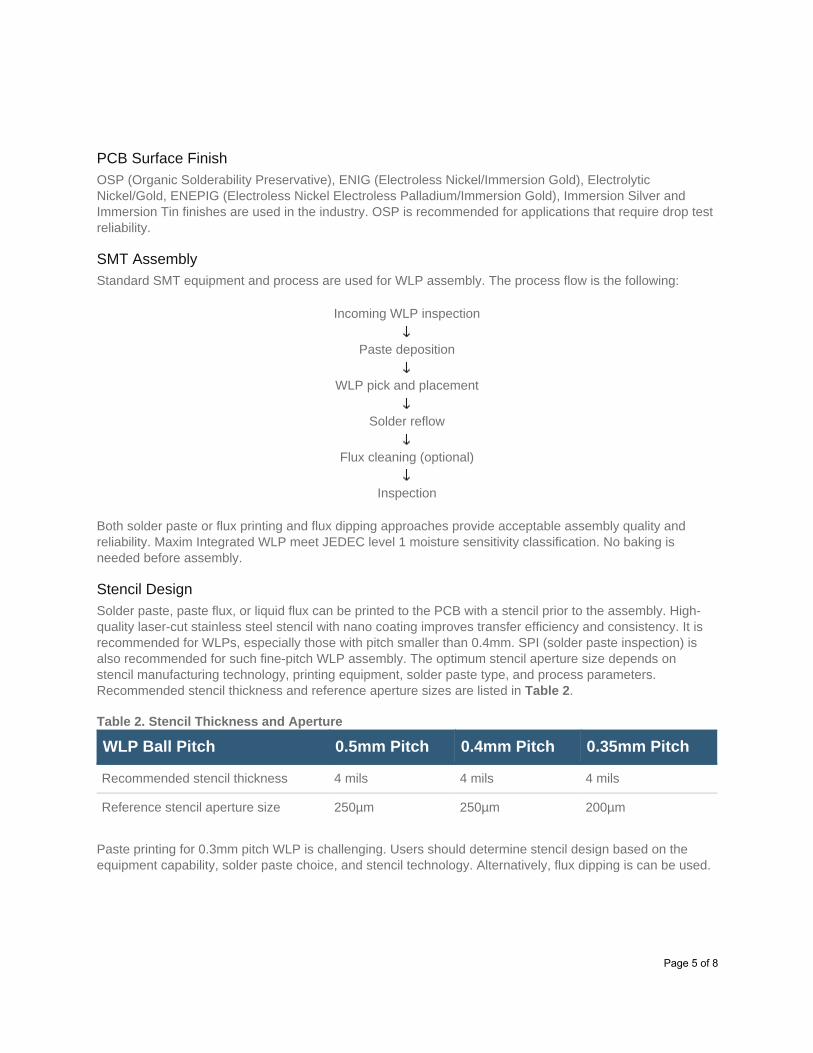
Stencil DesignSolder paste, paste flux, or liquid flux can be printed to the PCB with a stencil prior to the assembly. High-quality laser-cut stainless steel stencil with nano coating improves transfer efficiency and consistency. It is recommended for WLPs, especially those with pitch smaller than 0.4mm. SPI (solder paste inspection) is also recommended for such fine-pitch WLP assembly. The optimum stencil aperture size depends on stencil manufacturing technology, printing equipment, solder paste type, and process parameters. Recommended stencil thickness and reference aperture sizes are listed in Table 2.
Table 2. Stencil Thickness and Aperture
WLP Ball Pitch 0.5mm Pitch 0.4mm Pitch 0.35mm Pitch
Recommended stencil thickness 4 mils 4 mils 4 mils
Reference stencil aperture size 250µm 250µm 200µm
Paste printing for 0.3mm pitch WLP is challenging. Users should determine stencil design based on the equipment capability, solder paste choice, and stencil technology. Alternatively, flux dipping is can be used.
Page 5 of 8

Solder PasteConventional Pb-free solder pastes can be used for WLP assembly. Type 3 pastes can be used for 0.5mm and 0.4mm pitch WLP assembly while a type 4 paste is preferred for 0.35mm and 0.3mm pitch WLP. SnPb solder paste should not be used for Pb-free WLP assembly.
Automated Component Pick and PlaceStandard pick and place equipment can be used for placing Maxim Integrated WLP. A fine pitch IC packaging placement equipment is preferred for better accuracy. Plastic pick up nozzles are recommended. Pick and place force should not exceed 2N.
WLP body outline can be used for component recognition. For better placement accuracy, solder balls can be used for alignment. With this approach, a look-up camera is used to recognize the solder balls. The equipment enters the ball array itself to the footprint for better alignment accuracy.
ReflowAll Maxim Integrated WLPs are compatible with industry-standard solder reflow processes. An optimized reflow profile takes into account of flux type and all components to be soldered to the board. Use of nitrogen inert-atmosphere reflow is optional. It has demonstrated a better centering of the Pb-free WLP on the pads and less solder oxidation compared to air reflow.
Flux CleaningPost reflow cleaning is not recommended especially when a no-clean type solder paste is used. If cleaning is required, a spray-under-immersion or ultrasonic-immersion cleaning method is recommended. A thorough study of flux, paste, and cleaning solvent compatibility must be evaluated.
UnderfillIn general, underfill material is not required for WLP. In certain applications, underfill can enhance WLP mechanical robustness when proper underfill material is selected.
ReworkRework is not recommended. It should only be performed using a controlled and qualified process that prevents mechanical and ESD damage.
ReliabilityReliability requirements are listed in Table 3.
Page 6 of 8

Stress Specification Abbv Condition
No. of Lots/SS per Lot Duration/Acceptance
MSL Preconditioning
JESTD20 PC MSL1 3 lots/150 units
Visual and Electrical test
High JESD22-A103 HTS 150°C 3 lots/77 units 1000hrs/0 Fail
Table 3. Reliability Qualification Requirements
Temperature Storage
Temperature Cycling
JESD22-A104 TC -40°C to+125°C1 cycle/hr
3 lots/77 units 1000 cycles for array size ² 6x6/note
500 cycles for array size > 6x6/note
Operating Life Test
JESD22 A108 HTOL T = 135°C 3 lots/77 units 1000hrs/0 Fail
Drop Test JESD22-B111 DT Cond B 1 lot/60 units 150 drops/note
J
Note: Meet less than 5% failure rate at 90% confidence level at the number of cycles specified for the reliability stress.Thermal PerformanceThermal modeling is performed with JEDEC still air conditions. The junction-to-ambient thermal resistance values for 0.5mm and 0.4mm pitch WLP are listed in Table 4 and Table 5, respectively.
Table 4. Thermal Resistance of 0.5mm pitch WLP
Array Size Pitch (mm) θ (°C/W) for 1S0P Board θ (°C/W) for 2S2P Board
2x2 0.5 329.2 87.4
4x4 0.5 154.8 49.1
6x6 0.5 110.4 37.7
8x8 0.5 87.8 31.6
10x10 0.5 73.4 27.7
12x12 0.5 63.4 24.8
14x14 0.5 55.9 22.5
JA JA
Page 7 of 8

10x10 0.4 101.9 33.6
12x12 0.4 88.4 30.2
14x14 0.4 78.1 27.5
More InformationFor Technical Support: http://www.maximintegrated.com/en/supportFor Samples: http://www.maximintegrated.com/en/samplesOther Questions and Comments: http://www.maximintegrated.com/en/contact
Application Note 1891: http://www.maximintegrated.com/en/an1891APPLICATION NOTE 1891, AN1891, AN 1891, APP1891, Appnote1891, Appnote 1891 © 2014 Maxim Integrated Products, Inc.The content on this webpage is protected by copyright laws of the United States and of foreign countries. For requests to copy this content, contact us. Additional Legal Notices: http://www.maximintegrated.com/en/legal
Table 5. Thermal Resistance of 0.4mm pitch WLP
Array Size Pitch (mm) θ (°C/W) for 1S0P Board θ (°C/W) for 2S2P Board
2x2 0.4 434.5 102.6
4x4 0.4 209.7 57.9
6x6 0.4 151.3 45.7
8x8 0.4 121.2 38.2
JA JA
Page 8 of 8