WAFER ANALYSIS BY BSE ICP-MS - Chem Tracechemtrace.com/files/Wafer Analysis by BSE ICP MS...
1
WAFER ANALYSIS BY BSE ICP-MS BULK SILICON ETCH INDUCTIVELY COUPLED PLASMA MASS SPECTROMETRY What is BSE ICP-MS? Application 1. Implant 4. CVD: PECVD, LPCVD 2. Silicon Epitaxial 5. Sawing 3. CMP Advanced wet-chemistries etching of Si-based film or substrate allowing trace metals characterization across a large surface area within certain depth. This versatile technique allows single or multi step etching of film or substrate varying from 50Å to 100μm. Si or Poly Sub-surface trace metals by Multi Step BSE ICP-MS Bulk trace metals by Bulk Digestion Polysilicon or Silicon Substrate Method Detection Limits (E10 atoms/cm 2 ) Aluminum (Al) Antimony (Sb) Arsenic (As) Barium (Ba) Beryllium (Be) Bismuth (Bi) Boron (B) Cadmium (Cd) Calcium (Ca) Chromium (Cr) 5 0.05 0.5 0.05 5 0.02 10 0.1 5 1 MDL ELEMENTS Cobalt (Co) Copper (Cu) Gallium (Ga) Germanium (Ge) Iron (Fe) Lead (Pb) Lithium (Li) Magnesium (Mg) Manganese (Mn) Molybdenum (Mg) 0.2 1 0.2 0.2 3 0.05 1 5 0.05 0.5 MDL ELEMENTS Nickel (Ni) Potassium (K) Sodium (Na) Strontium (Sr) Tin (Sn) Titanium (Ti) Tungsten (W) Vanadium (V) Zinc (Zn) Zirconium (Zr) 0.5 5 5 0.05 0.1 2 0.5 0.5 1 0.05 MDL ELEMENTS Method detection limits (MDL) are based on 500Å etch depth 44050 Fremont Blvd Fremont, CA 94538 Phone: (510) 687-8000 © ChemTrace. All rights reserved. 12130 NE Ainsworth Circle, Suite #210 Portland, OR 97220 Phone: (503) 254-2828 www.ChemTrace.com CROSS SECTION VIEW OF POLYSILICON OR SILICON SUBSTRATE -- In-film by BSE ICP-MS
Transcript of WAFER ANALYSIS BY BSE ICP-MS - Chem Tracechemtrace.com/files/Wafer Analysis by BSE ICP MS...
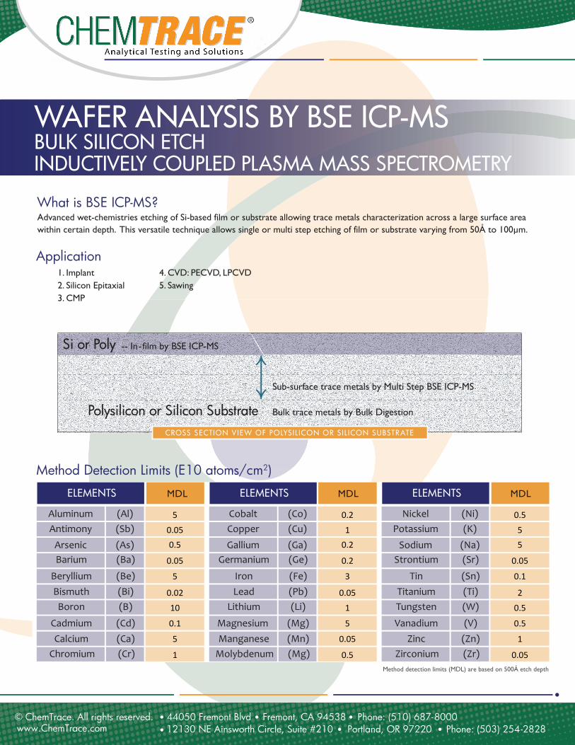
WAFER ANALYSIS BY BSE ICP-MSBULK SILICON ETCHINDUCTIVELY COUPLED PLASMA MASS SPECTROMETRY
What is BSE ICP-MS?
Application1. Implant 4. CVD: PECVD, LPCVD2. Silicon Epitaxial 5. Sawing3. CMP
Advanced wet-chemistries etching of Si-based film or substrate allowing trace metals characterization across a large surface area within certain depth. This versatile technique allows single or multi step etching of film or substrate varying from 50Å to 100µm.
Si or Poly
Sub-surface trace metals by Multi Step BSE ICP-MS
Bulk trace metals by Bulk Digestion Polysilicon or Silicon Substrate
Method Detection Limits (E10 atoms/cm2)
Aluminum (Al)Antimony (Sb)
Arsenic (As)Barium (Ba)
Beryllium (Be)Bismuth (Bi)
Boron (B)
Cadmium (Cd)Calcium (Ca)
Chromium (Cr)
5
0.05
0.5
0.05
5
0.02
10
0.1
5
1
MDLELEMENTS
Cobalt (Co)Copper (Cu)
Gallium (Ga)Germanium (Ge)
Iron (Fe)Lead (Pb)
Lithium (Li)
Magnesium (Mg)Manganese (Mn)
Molybdenum (Mg)
0.2
1
0.2
0.2
3
0.05
1
5
0.05
0.5
MDLELEMENTS
Nickel (Ni)Potassium (K)
Sodium (Na)Strontium (Sr)
Tin (Sn)Titanium (Ti)Tungsten (W)
Vanadium (V)Zinc (Zn)
Zirconium (Zr)
0.5
5
5
0.05
0.1
2
0.5
0.5
1
0.05
MDLELEMENTS
Method detection limits (MDL) are based on 500Å etch depth
44050 Fremont Blvd Fremont, CA 94538 Phone: (510) 687-8000 © ChemTrace. All rights reserved. 12130 NE Ainsworth Circle, Suite #210 Portland, OR 97220 Phone: (503) 254-2828 www.ChemTrace.com
CROSS SECTION VIEW OF POLYSIL ICON OR SIL ICON SUBSTRATE
-- In-film by BSE ICP-MS