W3 / W4 / W5 / W7/ W9 Control Head Models Service …® Digital Spectra® and Digital Spectra Plus...
126
ASTRO ® Digital Spectra ® and Digital Spectra Plus Mobile Radios W3 / W4 / W5 / W7/ W9 Control Head Models Service Manual
Transcript of W3 / W4 / W5 / W7/ W9 Control Head Models Service …® Digital Spectra® and Digital Spectra Plus...

ASTRO® Digital Spectra
®
and Digital Spectra Plus
Mobile Radios
W3 / W4 / W5 / W7/ W9
Control Head Models
Service Manual


tra®
lus
dios
W9elsual
77-O
Title Page ASTRO® Digital Specand Digital Spectra P
Mobile Ra
W3/W4/W5/W7/Control Head Mod
Service Man
Motorola, Inc.8000 West Sunrise BoulevardFort Lauderdale, Florida 33322 6881096C
i

ForewordThis manual covers the ASTRO® Digital Spectra® and Digital Spectra Plus control heads (Models W3, W4, W5, W7, and W9), unless otherwise specified. This manual provides sufficient information to enable qualified service shop technicians to troubleshoot and repair ASTRO® Digital Spectra® and Digital Spectra Plus control heads to the component level.
For details on radio operation, refer to the applicable manuals available separately. A list of related publications is provided in the section, “Related Publications,” on page ix.
Product Safety and RF Exposure Compliance
ATTENTION!
The radio that comes with this control head is restricted to occupational use only to satisfy FCC RF energy exposure requirements. Before using this product, read the RF energy awareness information and operating instructions in the Product Safety and RF Exposure booklet enclosed with your radio (Motorola Publication part number 68P81095C99) to ensure compliance with RF energy exposure limits.
For a list of Motorola-approved antennas, batteries, and other accessories, visit the following web site which lists approved accessories: http://www.motorola.com/cgiss/index.shtml
Manual Revisions
Changes which occur after this manual is printed are described in FMRs (Florida Manual Revisions). These FMRs provide complete replacement pages for all added, changed, and deleted items. To obtain FMRs, contact the Radio Parts Services Division (refer to “Appendix A, Replacement Parts Ordering”).
Computer Software Copyrights
The Motorola products described in this manual may include copyrighted Motorola computer programs stored in semiconductor memories or other media. Laws in the United States and other countries preserve for Motorola certain exclusive rights for copyrighted computer programs, including, but not limited to, the exclusive right to copy or reproduce in any form the copyrighted computer program. Accordingly, any copyrighted Motorola computer programs contained in the Motorola products described in this manual may not be copied, reproduced, modified, reverse-engineered, or distributed in any manner without the express written permission of Motorola. Furthermore, the purchase of Motorola products shall not be deemed to grant either directly or by implication, estoppel, or otherwise, any license under the copyrights, patents or patent applications of Motorola, except for the normal non-exclusive license to use that arises by operation of law in the sale of a product.
Document Copyrights
No duplication or distribution of this document or any portion thereof shall take place without the express written permission of Motorola. No part of this manual may be reproduced, distributed, or transmitted in any form or by any means, electronic or mechanical, for any purpose without the express written permission of Motorola.
Disclaimer
The information in this document is carefully examined, and is believed to be entirely reliable. However, no responsibility is assumed for inaccuracies. Furthermore, Motorola reserves the right to make changes to any products herein to improve readability, function, or design. Motorola does not assume any liability arising out of the applications or use of any product or circuit described herein; nor does it cover any license under its patent rights nor the rights of others.
Trademarks
MOTOROLA, the Stylized M logo, ASTRO, and Spectra are registered in the US Patent & Trademark Office. All other product or service names are the property of their respective owners.
© Motorola, Inc. 2003.
CAUTION: Before using this product, read the operating instruc-tions for safe usage contained in the Product Safety and RF Expo-sure booklet enclosed with your radio.
!C a u t i o n
ii

Table of Contents iii
Table of Contents
Foreword.........................................................................................................ii
Product Safety and RF Exposure Compliance ............................................................................................ iiManual Revisions ........................................................................................................................................ iiComputer Software Copyrights ...................................................................................................................iiDocument Copyrights .................................................................................................................................. iiDisclaimer.................................................................................................................................................... iiTrademarks ................................................................................................................................................. ii
Commercial Warranty ...................................................................................xi
Limited Warranty ........................................................................................................................................xiMOTOROLA COMMUNICATION PRODUCTS................................................................................xi
I. What This Warranty Covers And For How Long .....................................................................xiII. General Provisions .................................................................................................................xiIII. State Law Rights .................................................................................................................. xiiIV. How To Get Warranty Service ............................................................................................. xiiV. What This Warranty Does Not Cover.................................................................................... xiiVI. Patent And Software Provisions ......................................................................................... xiiiVII. Governing Law................................................................................................................... xiii
Chapter 1 Introduction ......................................................................... 1-1
1.1 Notations Used in This Manual...................................................................................................... 1-11.2 Control Head Features .................................................................................................................. 1-21.3 Control Heads................................................................................................................................ 1-2
1.3.1 W3 Control Head .............................................................................................................. 1-21.3.1.1 W3 Controls ............................................................................................................. 1-3
1.3.2 W4, W5, W7, and W9 Control Heads ............................................................................... 1-41.3.2.1 W4, W5, W7, and W9 Controls................................................................................ 1-6
Chapter 2 Basic Maintenance.............................................................. 2-1
2.1 Inspection ...................................................................................................................................... 2-12.2 Cleaning......................................................................................................................................... 2-1
2.2.1 Cleaning External Plastic Surfaces................................................................................... 2-12.2.2 Cleaning Internal Circuit Boards and Components........................................................... 2-1
2.3 Handling Precautions..................................................................................................................... 2-2
Chapter 3 Theory of Operation............................................................ 3-1
3.1 W3 Control Head ........................................................................................................................... 3-13.1.1 SB9600 Serial Bus Interface............................................................................................. 3-13.1.2 Display Circuit ................................................................................................................... 3-13.1.3 Keypad Side Keys and Top Keys ..................................................................................... 3-23.1.4 Microphone Preamplifier and PTT .................................................................................... 3-2
6881096C77-O September 26, 2003
iv Table of Contents
3.1.5 On-/Off-Hook Control ........................................................................................................ 3-33.1.6 Backlight Circuit ................................................................................................................ 3-33.1.7 Power Supply.................................................................................................................... 3-33.1.8 Status LEDs ...................................................................................................................... 3-33.1.9 Jumper Selection .............................................................................................................. 3-33.1.10 Power On/Off .................................................................................................................... 3-43.1.11 Miscellaneous Functions................................................................................................... 3-4
3.2 W4, W5, and W7 Control Heads.................................................................................................... 3-43.2.1 Power Switch/Ignition........................................................................................................ 3-43.2.2 Voltage Regulator ............................................................................................................. 3-53.2.3 Microcomputer ..................................................................................................................3-53.2.4 Interface Circuitry.............................................................................................................. 3-53.2.5 Reset................................................................................................................................. 3-63.2.6 Bus Busy........................................................................................................................... 3-63.2.7 Serial Bus Data ................................................................................................................. 3-63.2.8 Push-To-Talk (PTT) .......................................................................................................... 3-73.2.9 Hang-Up Button (HUB) .....................................................................................................3-73.2.10 Ignition Sense Circuitry .....................................................................................................3-73.2.11 Keypad Scan..................................................................................................................... 3-73.2.12 Vacuum Fluorescent (VF) Voltage Converter Circuitry..................................................... 3-73.2.13 Vacuum Fluorescent Display Driver IC ............................................................................. 3-83.2.14 Vacuum Fluorescent Display ............................................................................................ 3-83.2.15 Backlight LEDs..................................................................................................................3-8
3.3 W9 Control Head ........................................................................................................................... 3-83.3.1 Display .............................................................................................................................. 3-83.3.2 W9 Controls and Indicators............................................................................................... 3-93.3.3 Control Board.................................................................................................................... 3-9
3.3.3.1 Microprocessor ........................................................................................................ 3-93.3.3.2 Watchdog Timer....................................................................................................... 3-93.3.3.3 Bus Transceiver ..................................................................................................... 3-103.3.3.4 Vacuum Fluorescent Voltage Converter ................................................................ 3-103.3.3.5 Vehicle Interface Ports........................................................................................... 3-103.3.3.6 Power Supply.........................................................................................................3-103.3.3.7 Ignition Sense Circuits ........................................................................................... 3-103.3.3.8 EEPROM Write-Protect Circuit .............................................................................. 3-11
3.3.4 Display Board.................................................................................................................. 3-113.3.4.1 VF Display..............................................................................................................3-113.3.4.2 VF Display Driver ...................................................................................................3-113.3.4.3 Status LEDs........................................................................................................... 3-113.3.4.4 Backlight LEDs....................................................................................................... 3-11
3.3.5 Default Jumper Settings.................................................................................................. 3-113.4 Vehicle Interface Port (VIP) .........................................................................................................3-12
3.4.1 W4, W5, and W7 Control Heads..................................................................................... 3-123.4.1.1 VIP Output Connections ........................................................................................ 3-12
3.4.1.1.1 Dash-Mount Installations ................................................................................ 3-123.4.1.1.2 Remote-Mount Installations ............................................................................ 3-13
3.4.1.2 VIP Input Connections (Remote-Mount Only)........................................................ 3-133.4.2 W9 Control Heads........................................................................................................... 3-14
3.4.2.1 VIP Output Connections ........................................................................................ 3-143.4.2.2 VIP Input Connections ........................................................................................... 3-14
Chapter 4 Test Equipment and Service Aids ..................................... 4-1
September 26, 2003 6881096C77-O

Table of Contents v
4.1 Recommended Test Equipment and Service Aids ........................................................................ 4-1
Chapter 5 Troubleshooting................................................................. 5-1
5.1 Required Tools and Supplies......................................................................................................... 5-15.2 Troubleshooting Waveforms.......................................................................................................... 5-2
5.2.1 ASTRO Digital Spectra Waveforms.................................................................................. 5-25.3 Replacing the Vacuum Fluorescent Display (W4, W5, and W7 Control Heads) ........................... 5-5
5.3.1 Removing the Display....................................................................................................... 5-55.3.2 Installing the Display ......................................................................................................... 5-5
5.4 Replacing the Remote Back-Housing Interface Board .................................................................. 5-55.4.1 W4, W5, and W7 Control Heads....................................................................................... 5-5
5.5 Replacing the Remote Interconnect Board.................................................................................... 5-65.5.1 Low-/Mid-Power Radios.................................................................................................... 5-65.5.2 High-Power Radios........................................................................................................... 5-6
5.6 Replacing the Control-Head Board................................................................................................ 5-75.6.1 W3 Control Heads ............................................................................................................ 5-75.6.2 W4, W5, and W7 Control Heads....................................................................................... 5-85.6.3 W9 Control Heads .......................................................................................................... 5-10
5.7 Final Reassembly–W3 Control Head........................................................................................... 5-115.8 Troubleshooting Charts ............................................................................................................... 5-12
Chapter 6 Radio Connectors ............................................................... 6-1
6.1 Radio Connectors .......................................................................................................................... 6-26.2 Radio Connector Locations ........................................................................................................... 6-36.3 Extender Cable (P501) .................................................................................................................. 6-46.4 Control-Head Cabling Diagram...................................................................................................... 6-4
Chapter 7 Exploded Views and Parts Lists ........................................ 7-1
7.1 Model W3 Hand-Held Control Head Exploded View ..................................................................... 7-27.2 W4 Rotary Control Head Exploded View...................................................................................... 7-37.3 W5 and W7 Pushbutton Control Head Exploded View................................................................. 7-47.4 W9 Pushbutton Control Head Exploded View .............................................................................. 7-57.5 HMN1080A, HMN1061A, HMN1079A Microphone Exploded View .............................................. 7-67.6 Small Pushbutton Parts ................................................................................................................. 7-77.7 Large Pushbutton Parts ................................................................................................................. 7-7
Chapter 8 Schematics, Overlays, and Parts Lists ............................. 8-1
8.1 List of Schematics, Component Location Diagrams, and Parts Lists ............................................ 8-1
Appendix A Replacement Parts Ordering..............................................A-1
A.1 Basic Ordering Information ............................................................................................................A-1A.2 Motorola Online .............................................................................................................................A-1A.3 Mail Orders ....................................................................................................................................A-1A.4 Telephone Orders..........................................................................................................................A-2
6881096C77-O September 26, 2003

vi Table of Contents
A.5 Fax Orders .....................................................................................................................................A-2A.6 Parts Identification .........................................................................................................................A-2A.7 Product Customer Service .............................................................................................................A-2
Index..................................................................................................... Index-1
September 26, 2003 6881096C77-O

List of Figures vii
6881096C77-O September 26, 2003
List of Figures
Figure 1-1. Typical W3 Hand-Held Control Head.................................................................................... 1-3Figure 1-2. Typical W4 Rotary Control Head........................................................................................... 1-4Figure 1-3. Typical W5 Pushbutton Control Head................................................................................... 1-4Figure 1-4. Typical W7 Pushbutton Control Head................................................................................... 1-5Figure 1-5. Typical W9 Pushbutton Control Head................................................................................... 1-5Figure 3-1. Astro Spectra Control Head Block Diagram.......................................................................... 3-4Figure 3-2. Cabling Interconnect Diagram for Dash Mount................................................................... 3-13Figure 3-3. Cabling Interconnect Diagram for Remote Mount............................................................... 3-13Figure 5-1. Replacing the Vacuum Fluorescent Display ......................................................................... 5-5Figure 5-2. Model W4 Rotary Control Head Assembly Screw and Snap Sequence............................... 5-8Figure 5-3. Models W5 and W7 Pushbutton Control Head Assembly Screw Sequence ........................ 5-8Figure 5-4. W9 Control Head Control Board and Display Board........................................................... 5-10Figure 6-1. J0103 Remote-Mount Control Head Connector.................................................................... 6-2Figure 6-2. J5 Control Cable for Remote-Mount Control Head............................................................... 6-2Figure 6-3. J6 Radio Operations Connector............................................................................................ 6-2Figure 6-4. J2 Rear Accessory Connector .............................................................................................. 6-2Figure 6-5. P104 Microphone Jack ......................................................................................................... 6-2Figure 6-6. Dash-Mount Radio Connector Locations.............................................................................. 6-3Figure 6-7. Remote-Mount Radio Connector Locations.......................................................................... 6-3Figure 6-8. Command Board Connector Locations................................................................................. 6-3Figure 6-9. VOCON Board Connector Locations .................................................................................... 6-3Figure 6-10. P501 Extender Cable............................................................................................................ 6-4Figure 6-11. Control-Head Cabling Diagram............................................................................................. 6-4Figure 7-1. W3 Hand-Held Control Head Exploded View ....................................................................... 7-2Figure 7-2. W4 Rotary Control Head Exploded View .............................................................................. 7-3Figure 7-3. W5 and W7 Pushbutton Control Head Exploded View ......................................................... 7-4Figure 7-4. W9 Pushbutton Control Head Exploded View ...................................................................... 7-5Figure 7-5. HMN1080A, HMN1061A, HMN1079A Microphone Exploded View...................................... 7-6

viii Related Publications
List of Tables
Table 1-1. ASTRO Digital Spectra/Spectra Plus Basic Features ........................................................... 1-2Table 1-2. 12-Button Keypad (W7 and W9) ........................................................................................... 1-7Table 3-1. W3 Jumper Selection............................................................................................................ 3-3Table 3-2. Types of Operations.............................................................................................................. 3-4Table 3-3. Serial Data Bus Logic............................................................................................................ 3-6Table 3-4. PTT Logic States................................................................................................................... 3-7Table 3-5. HUB Logic States ..................................................................................................................3-7Table 3-6. Standard Jumper Configurations......................................................................................... 3-11Table 3-7. VIP Output Connections ..................................................................................................... 3-14Table 3-8. VIP Input Connections ........................................................................................................ 3-14Table 4-1. Recommended Motorola Test Equipment and Service Aids .................................................4-1Table 5-1. Required Tools and Supplies ................................................................................................ 5-1Table 7-1. Exploded Views..................................................................................................................... 7-1Table 7-2. W3 Hand-Held Control Head Exploded View Parts List........................................................ 7-2Table 7-3. Model W4 Rotary Control Head Parts List ............................................................................ 7-3Table 7-4. W5 and W7 Pushbutton Control Head Parts List .................................................................. 7-4Table 7-5. W9 Pushbutton Control Head Parts List .............................................................................. 7-5Table 7-6. HMN1080A, HMN1061A, HMN1079A Microphone Parts List............................................... 7-6Table 7-7. Small Pushbutton Parts List .................................................................................................. 7-7Table 7-8. Large Pushbutton Parts List.................................................................................................. 7-7
September 26, 2003 6881096C77-O

List of Tables ix
Related PublicationsASTRO Digital Spectra and Digital Spectra Plus Model W3 User’s Guide ..................................6881090C61ASTRO Digital Spectra and Digital Spectra Plus Models W4, W5, W7, and W9 User’s Guide ..6881090C62ASTRO Digital Spectra Hand-Held Control Head User’s Guide (Model W3) ..............................6881073C25ASTRO Digital Spectra (Model W4, W5, W7, and W9) User’s Guide..........................................6881074C80ASTRO Digital Spectra and Digital Spectra Plus Mobile Radios Detailed Service Manual .........6881076C25ASTRO Digital Spectra Mobile Radios Dual Control Head Radio System Service Manual.........6881091C78ASTRO Spectra and Digital Spectra FM Two-Way Mobile Radios Installation Manual ...............6881070C85ASTRO Spectra Motorcycle Radios Supplemental Installation Manual...................................... 6880103W01CPS Programming Installation Guide ..........................................................................................6881095C44KVL 3000 User’s Manual ............................................................................................................. 6881131E16
6881096C77-O September 26, 2003
x List of Tables
Notes
September 26, 2003 6881096C77-O

Commercial Warranty xi
Commercial Warranty
Limited Warranty
MOTOROLA COMMUNICATION PRODUCTS
I. What This Warranty Covers And For How Long
MOTOROLA INC. (“MOTOROLA”) warrants the MOTOROLA manufactured Communication Products listed below (“Product”) against defects in material and workmanship under normal use and service for a period of time from the date of purchase as scheduled below:
Motorola, at its option, will at no charge either repair the Product (with new or reconditioned parts), replace it (with a new or reconditioned Product), or refund the purchase price of the Product during the warranty period provided it is returned in accordance with the terms of this warranty. Replaced parts or boards are warranted for the balance of the original applicable warranty period. All replaced parts of Product shall become the property of MOTOROLA.
This express limited warranty is extended by MOTOROLA to the original end user purchaser only and is not assignable or transferable to any other party. This is the complete warranty for the Product manufactured by MOTOROLA. MOTOROLA assumes no obligations or liability for additions or modifications to this warranty unless made in writing and signed by an officer of MOTOROLA. Unless made in a separate agreement between MOTOROLA and the original end user purchaser, MOTOROLA does not warrant the installation, maintenance or service of the Product.
MOTOROLA cannot be responsible in any way for any ancillary equipment not furnished by MOTOROLA which is attached to or used in connection with the Product, or for operation of the Product with any ancillary equipment, and all such equipment is expressly excluded from this warranty. Because each system which may use the Product is unique, MOTOROLA disclaims liability for range, coverage, or operation of the system as a whole under this warranty.
II. General Provisions
This warranty sets forth the full extent of MOTOROLA'S responsibilities regarding the Product. Repair, replacement or refund of the purchase price, at MOTOROLA's option, is the exclusive remedy. THIS WARRANTY IS GIVEN IN LIEU OF ALL OTHER EXPRESS WARRANTIES. IMPLIED WARRANTIES, INCLUDING WITHOUT LIMITATION, IMPLIED WARRANTIES OF MERCHANTABILITY AND FITNESS FOR A PARTICULAR PURPOSE, ARE LIMITED TO THE DURATION OF THIS LIMITED WARRANTY. IN NO EVENT SHALL MOTOROLA BE LIABLE FOR DAMAGES IN EXCESS OF THE PURCHASE PRICE OF THE PRODUCT, FOR ANY LOSS OF USE, LOSS OF TIME, INCONVENIENCE, COMMERCIAL LOSS, LOST PROFITS OR SAVINGS OR OTHER INCIDENTAL, SPECIAL OR CONSEQUENTIAL DAMAGES ARISING OUT OF THE USE OR INABILITY TO USE SUCH PRODUCT, TO THE FULL EXTENT SUCH MAY BE DISCLAIMED BY LAW.
ASTRO Digital Spectra and Digital Spectra Plus Units
One (1) Year
Product Accessories One (1) Year
6881096C77-O September 26, 2003

xii Commercial Warranty
III. State Law Rights
SOME STATES DO NOT ALLOW THE EXCLUSION OR LIMITATION OF INCIDENTAL OR CONSEQUENTIAL DAMAGES OR LIMITATION ON HOW LONG AN IMPLIED WARRANTY LASTS, SO THE ABOVE LIMITATION OR EXCLUSIONS MAY NOT APPLY.
This warranty gives specific legal rights, and there may be other rights which may vary from state to state.
IV. How To Get Warranty Service
You must provide proof of purchase (bearing the date of purchase and Product item serial number) in order to receive warranty service and, also, deliver or send the Product item, transportation and insurance prepaid, to an authorized warranty service location. Warranty service will be provided by Motorola through one of its authorized warranty service locations. If you first contact the company which sold you the Product, it can facilitate your obtaining warranty service. You can also call Motorola at 1-888-567-7347 US/Canada.
V. What This Warranty Does Not Cover
A. Defects or damage resulting from use of the Product in other than its normal and customary manner.
B. Defects or damage from misuse, accident, water, or neglect.
C. Defects or damage from improper testing, operation, maintenance, installation, alteration, modification, or adjustment.
D. Breakage or damage to antennas unless caused directly by defects in material workmanship.
E. A Product subjected to unauthorized Product modifications, disassemblies or repairs (includ-ing, without limitation, the addition to the Product of non-Motorola supplied equipment) which adversely affect performance of the Product or interfere with Motorola’s normal warranty inspection and testing of the Product to verify any warranty claim.
F. Product which has had the serial number removed or made illegible.
G. Rechargeable batteries if:
- any of the seals on the battery enclosure of cells are broken or show evidence of tamper-ing.
- the damage or defect is caused by charging or using the battery in equipment or service other than the Product for which it is specified.
H. Freight costs to the repair depot.
I. A Product which, due to illegal or unauthorized alteration of the software/firmware in the Prod-uct, does not function in accordance with MOTOROLA’s published specifications or the FCC type acceptance labeling in effect for the Product at the time the Product was initially distrib-uted from MOTOROLA.
J. Scratches or other cosmetic damage to Product surfaces that does not affect the operation of the Product.
K. Normal and customary wear and tear.
September 26, 2003 6881096C77-O

Commercial Warranty xiii
VI. Patent And Software Provisions
MOTOROLA will defend, at its own expense, any suit brought against the end user purchaser to the extent that it is based on a claim that the Product or parts infringe a United States patent, and MOTOROLA will pay those costs and damages finally awarded against the end user purchaser in any such suit which are attributable to any such claim, but such defense and payments are conditioned on the following:
A. that MOTOROLA will be notified promptly in writing by such purchaser of any notice of such claim;
B. that MOTOROLA will have sole control of the defense of such suit and all negotiations for its settlement or compromise; and
C. should the Product or parts become, or in MOTOROLA’s opinion be likely to become, the subject of a claim of infringement of a United States patent, that such purchaser will permit MOTOROLA, at its option and expense, either to procure for such purchaser the right to con-tinue using the Product or parts or to replace or modify the same so that it becomes nonin-fringing or to grant such purchaser a credit for the Product or parts as depreciated and accept its return. The depreciation will be an equal amount per year over the lifetime of the Product or parts as established by MOTOROLA.
MOTOROLA will have no liability with respect to any claim of patent infringement which is based upon the combination of the Product or parts furnished hereunder with software, apparatus or devices not furnished by MOTOROLA, nor will MOTOROLA have any liability for the use of ancillary equipment or software not furnished by MOTOROLA which is attached to or used in connection with the Product. The foregoing states the entire liability of MOTOROLA with respect to infringement of patents by the Product or any parts thereof.
Laws in the United States and other countries preserve for MOTOROLA certain exclusive rights for copyrighted MOTOROLA software such as the exclusive rights to reproduce in copies and distribute copies of such Motorola software. MOTOROLA software may be used in only the Product in which the software was originally embodied and such software in such Product may not be replaced, copied, distributed, modified in any way, or used to produce any derivative thereof. No other use including, without limitation, alteration, modification, reproduction, distribution, or reverse engineering of such MOTOROLA software or exercise of rights in such MOTOROLA software is permitted. No license is granted by implication, estoppel or otherwise under MOTOROLA patent rights or copyrights.
VII. Governing Law
This Warranty is governed by the laws of the State of Illinois, USA.
6881096C77-O September 26, 2003

xiv Commercial Warranty
Notes
September 26, 2003 6881096C77-O

Chapter 1 Introduction
ASTRO Digital Spectra and Digital Spectra Plus control heads are available in five radio models: W3, W4, W5, W7, and W9. This chapter describes the control heads used with these radios.
1.1 Notations Used in This ManualThroughout the text in this publication, you will notice the use of note, caution, warning, and danger notations. These notations are used to emphasize that safety hazards exist, and care must be taken and observed.
NOTE: An operational procedure, practice, or condition that is essential to emphasize.
CAUTION indicates a potentially hazardous situation which, if not avoided, might result in equipment damage.
WARNING indicates a potentially hazardous situation which, if not avoided, could result in death or injury.
DANGER indicates an imminently hazardous situation which, if not avoided, will result in death or injury.
!C a u t i o n
!W A R N I N G
!
D A N G E R
!

1-2 Introduction: Control Head Features
1.2 Control Head FeaturesThe table below outlines the basic features of the five control heads covered in this manual.
1.3 Control Heads The control heads used with ASTRO Digital Spectra and Digital Spectra Plus radios have microprocessor circuitry that operates the standard and optional features built into the system. The control-head design allows for installation in even the smallest of vehicles. The control head may be field-programmed to add options or alter the information stored in certain areas of its electronic memory.
The following sections describe the control head used by each of the five models.
1.3.1 W3 Control Head
The W3 Hand-Held Control Head (HHCH) is shown below. THe HHCH has been designed as an alternative to the standard radio control-head approach. It can emulate most radio control-head functions, including LCD display, volume control, power On/Off, and mode. The HHCH can either replace the radio control head or be used in dual-control applications, either in conjunction with a radio control head or another HHCH.
Table 1-1. ASTRO Digital Spectra/Spectra Plus Basic Features
Feature W3 W4 W5 W7 W9
Display 2 line/14 characters Liquid-Crystal Display (LCD) with 8 Status Annunciators
1 line/8 charactersVacuum Fluorescent Display
1 line/8 charactersVacuum Fluorescent Display
1 line/8 charactersVacuum Fluorescent Display
1 line/11 charactersVacuum Fluorescent Display
Mode & Volume Controls
Rocker Switches Rotary Mode & Volume Controls
Rocker Switch Mode & Volume Controls
Rocker Switch Mode & Volume Controls
Rocker Switch Mode & Volume Controls
Numeric Keypad
Yes No No Yes Yes
Channel Capability (Digital Spectra)
255 128 128 255 255
Channel Capability (Digital Spectra Plus)
512 128 128 512 512
Remote Mount Available Available Available Available Available
Dash Mount Available Available Available Available Not Available
September 26, 2003 6881096C77-O

Introduction: Control Heads 1-3
Figure 1-1. Typical W3 Hand-Held Control Head
1.3.1.1 W3 Controls
On/Off Button (T1): Turns the radio on and off. Can be used as an additional programmable button if the on/off function is not used.
Orange Programmable Button (T2): Programmed at the factory for emergency use. Field programmable by a qualified radio technician.
Programmable Button (T3): Field programmable by a qualified radio technician.
LED Indicator: Green/red light-emitting diode. Indicates operating status.
Display: 2-line by 14-character display. Provides visual information about many radio features.
Keypad. Provides control of, and data interface with, many features.
Programmable Side Button 1 (S1): Field programmable by a qualified radio technician.
Programmable Side Button 2 (S2): Field programmable by a qualified radio technician.
Programmable Side Button 3 (S3): Field programmable by a qualified radio technician.
Mode Control: Used for selecting modes and programming menus.
Volume Control: Used for selecting volume level, editing names, and making certain radio adjustments.
Push-To-Talk (PTT) Button: Engages the transmitter.
MODE
HOME
2ABC1 Q Z 3DEF
4GHI 5JKL 6MNO
7PRS 8TUV 9WXY
0
VOL
Side Button 1 (S1)
Side Button 2 (S2)
Side Button 3 (S3)
On/OffButton(T1)
Push-To-Talk(PTT) Switch
LEDIndicator
AlphanumericKeypad
VolumeControl Mode Control
Orange ProgrammableButton(T2)
ProgrammableButton(T3)
Display
Button
6881096C77-O September 26, 2003
1-4 Introduction: Control Heads
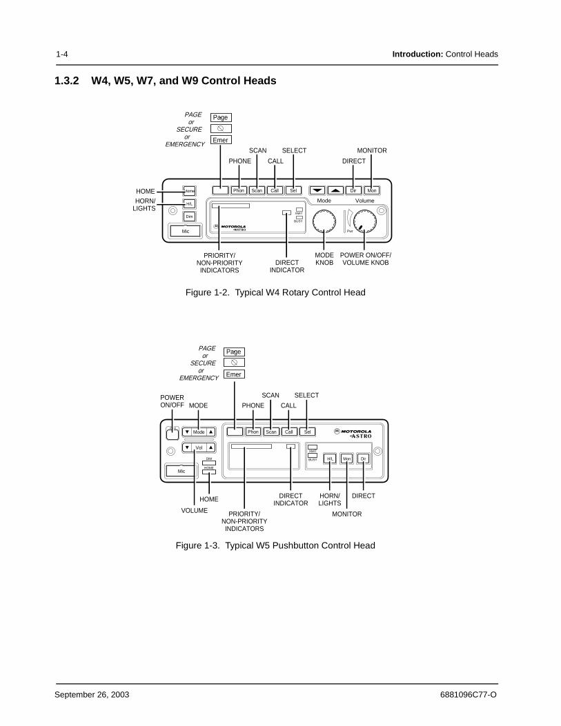
1.3.2 W4, W5, W7, and W9 Control Heads
Figure 1-2. Typical W4 Rotary Control Head
Figure 1-3. Typical W5 Pushbutton Control Head
PHONE
PAGEor
SECUREor
EMERGENCY
Page
Emer
CALL DIRECT
XMIT
BUSY
Mode Volume
Pwr
Phon Call SelScan
Mic
Home
Dim
H/L
Dir Mon
SCAN SELECT MONITOR
MODEKNOB
POWER ON/OFF/VOLUME KNOB
HOMEHORN/
LIGHTS
PRIORITY/NON-PRIORITYINDICATORS
DIRECTINDICATOR
Mode
Vol
Mic
Phon Call Sel
H/L Mon Dir
PWR
Scan
XMIT
BUSYDIM
HOME
MODEPOWERON/OFF
PAGEor
SECUREor
EMERGENCY
Page
Emer
PHONE
SCAN
CALL
SELECT
VOLUME PRIORITY/NON-PRIORITYINDICATORS
DIRECTINDICATOR
HORN/LIGHTS
MONITOR
DIRECTHOME
September 26, 2003 6881096C77-O
Introduction: Control Heads 1-5
Figure 1-4. Typical W7 Pushbutton Control Head
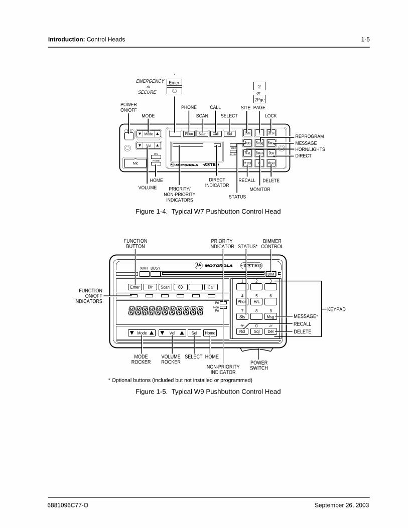
Figure 1-5. Typical W9 Pushbutton Control Head
POWERON/OFF
2
2Pgeor
SITE
LOCK
MESSAGEREPROGRAM
DIRECTO #Del Rcl
Mode
Vol
Mic
Phon Call SelPWR
Scan
XMIT
BUSYDIM
HOME
1Ste 2 3Lck
4Sts 5Rpg 6Msg
7H/L 8Mon 9Dir
MODE
EMERGENCYor
SECURE
Emer
PHONE
SCAN
CALL
SELECT
PAGE
VOLUME
DIRECTINDICATOR
DELETERECALL
MONITOR
STATUS
HORN/LIGHTS
HOME
PRIORITY/NON-PRIORITYINDICATORS
XMIT BUSY
CallScanEmer
DIM
PriNon
Pri
1 2 3
4 5 6
7 8 9
Mode Vol Sel Home
Phon H/L
Rcl Sql Del
Dir
Sts Msg
VOLUMEROCKER
MODEROCKER
SELECT HOME
KEYPAD
RECALLDELETE
DIMMERCONTROL
PRIORITYINDICATOR
FUNCTIONBUTTON
NON-PRIORITYINDICATOR
FUNCTIONON/OFF
INDICATORS
* Optional buttons (included but not installed or programmed)
MESSAGE*
POWERSWITCH
STATUS*
0
6881096C77-O September 26, 2003

1-6 Introduction: Control Heads
1.3.2.1 W4, W5, W7, and W9 Controls
Power Switch (PWR): Turns the radio and its accessories on or off. The Power switch is part of the rotary volume knob on the W4 model, a push-type switch on the W5 and W7 models, and a slide switch on the right-hand bottom surface of the W9 model.
Mode Switch: Used for selecting modes and programming menus. The Mode switch is a rotary switch on the W4 model and a rocker switch on the W5, W7, and W9 models. Press the right side of the rocker switch to increase the mode number and the left side to decrease the mode number. Press and hold the switch to scroll the mode number up or down. The mode names appear in the display window.
Volume Switch: Used for selecting the volume level, editing names, and making certain radio adjustments. The Volume switch is a rotary switch on the W4 model and a rocker switch on the W5, W7, and W9 models. On the pushbutton models, pressing and releasing the Volume switch checks the volume setting. Your display will show “VOLUME_ _” and a number value (0-15). Pressing and holding the left side decreases the volume. The number value scrolls up or down to your desired level. The Volume rocker switch also controls the volume level of the public address (PA) and external radio speaker (Ex Rd) options when they are enabled. The display window shows “PA VOL _ _” when public address is on and the Volume rocker switch is pressed.
Dim Button: Used to control the brightness of the display and button backlighting. When you turn on the system, the display comes on at the brightness level it was on before the system was last turned off. Press the DIM button once to reduce the brightness of the display to medium level and twice for low brightness level. Press the DIM button a third time to turn the display and button backlighting off. This is called the “surveillance” mode.
Home Button: Used for restoring preprogrammed mode, establishing programmed mode, selecting programming entries, etc. Press the Home button to go to the radio’s preprogrammed “home” mode. On the W7 models, you can use the Home button instead of the Mode switch to change modes. Hold the Home button until a beep sounds to enter the configuration state. The display shows an entry prompt. Use the keypad to enter your new mode choice and press the Home button again. Your mode is now changed without scrolling.
Select Button: Used to configure radio options.
Option Buttons: Used for turning options on and off, such as Phone, Scan, Emergency Call, and Secure.
Display: The vacuum fluorescent (VF) display’s primary function is to display mode numbers, mode names, volume level, and the status of options. It also functions as an on-off indicator for the entire system and plays an integral role in the operator’s reconfiguration of options. The display is 8 characters on W4, W5, and W7 models and 11 characters on the W9 model.
XMIT and BUSY Indicators: The XMIT indicator lights when the radio is transmitting. The BUSY indicator lights when the selected channel is busy.
Scan Indicators: When scan operation detects activity on a non-priority (NON-PRI) channel, the NON-PRI indicator light comes on. Activity on a second priority channel causes the priority (PRI) indicator to light. First priority channel activity causes PRI to flash.
12-Button Keypad (W7 and W9): Used to change the status of options and for entering numbers. Several keys serve multiple functions. The following buttons can be programmed to W7 and W9 control heads. The table below describes the buttons preinstalled on the W7 model. (See the ASTRO Digital Spectra or Digital Spectra Plus User’s Guide for a complete description of keypad operation.)
September 26, 2003 6881096C77-O
Introduction: Control Heads 1-7
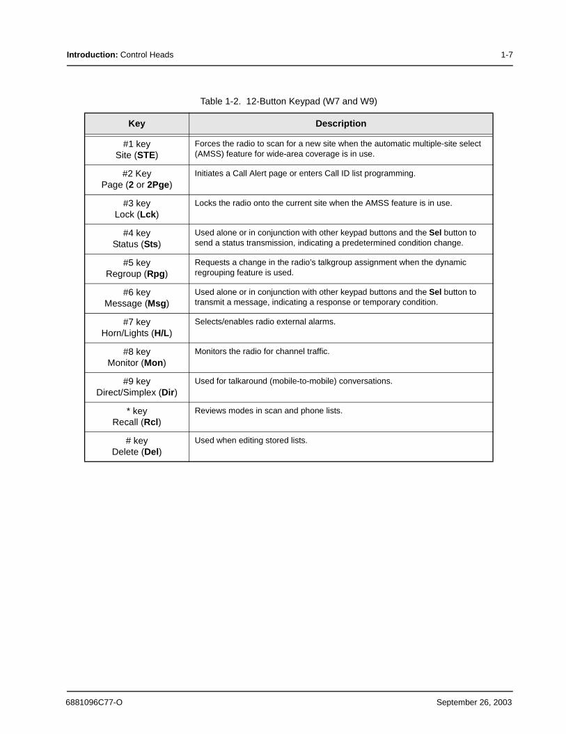
Table 1-2. 12-Button Keypad (W7 and W9)
Key Description
#1 keySite (STE)
Forces the radio to scan for a new site when the automatic multiple-site select (AMSS) feature for wide-area coverage is in use.
#2 KeyPage (2 or 2Pge)
Initiates a Call Alert page or enters Call ID list programming.
#3 keyLock (Lck)
Locks the radio onto the current site when the AMSS feature is in use.
#4 keyStatus (Sts)
Used alone or in conjunction with other keypad buttons and the Sel button to send a status transmission, indicating a predetermined condition change.
#5 keyRegroup (Rpg)
Requests a change in the radio’s talkgroup assignment when the dynamic regrouping feature is used.
#6 keyMessage (Msg)
Used alone or in conjunction with other keypad buttons and the Sel button to transmit a message, indicating a response or temporary condition.
#7 keyHorn/Lights (H/L)
Selects/enables radio external alarms.
#8 keyMonitor (Mon)
Monitors the radio for channel traffic.
#9 keyDirect/Simplex (Dir)
Used for talkaround (mobile-to-mobile) conversations.
* keyRecall (Rcl)
Reviews modes in scan and phone lists.
# keyDelete (Del)
Used when editing stored lists.
6881096C77-O September 26, 2003

1-8 Introduction: Control Heads
Notes
September 26, 2003 6881096C77-O

Chapter 2 Basic Maintenance
This chapter describes inspection, cleaning, and handling precautions for the control heads. Each of these topics provides information vital to the successful operation and maintenance of your radio.
2.1 InspectionCheck that the external surfaces of the control head are clean, and that all external controls and switches are functional. A detailed inspection of the interior electronic circuitry is not needed.
2.2 CleaningThe following procedures describe the recommended cleaning agents and the methods to be used when cleaning the external and internal surfaces of the control head. These surfaces should be cleaned whenever a periodic visual inspection reveals the presence of smudges, grease, and/or grime. Internal surfaces should be cleaned only when the control head is disassembled for servicing or repair.
The only recommended agent for cleaning the external control head surfaces is a 0.5% solution of a mild dishwashing detergent in water. The only factory recommended liquid for cleaning the printed circuit boards and their components is isopropyl alcohol (70% by volume).
2.2.1 Cleaning External Plastic Surfaces
The detergent-water solution should be applied sparingly with a stiff, non-metallic, short-bristled brush to work all loose dirt away from the control head. A soft, absorbent, lint-free cloth or tissue should be used to remove the solution and dry the control head. Make sure that no water remains entrapped near the connectors, cracks, or crevices.
2.2.2 Cleaning Internal Circuit Boards and Components
Isopropyl alcohol may be applied with a stiff, non-metallic, short-bristled brush to dislodge embedded or caked materials located in hard-to-reach areas.
Alcohol is a high-wetting liquid and can carry contamination into unwanted places if an excessive quantity is used. Make sure that controls or tunable components are not soaked with the liquid. Do not use high-pressure air to hasten the drying process, since this could cause the liquid to puddle and collect in unwanted places.
Upon completion of the cleaning process, use a soft, absorbent, lint-free cloth to dry the area.
NOTE: Always use a fresh supply of alcohol and a clean container to prevent contamination by dissolved material (from previous usage).
The effects of certain chemicals and their vapors can have harmful results on certain plastics. Aerosol sprays, tuner cleaners, and other chemicals should be avoided.
!C a u t i o n
2-2 Basic Maintenance: Handling Precautions
2.3 Handling Precautions
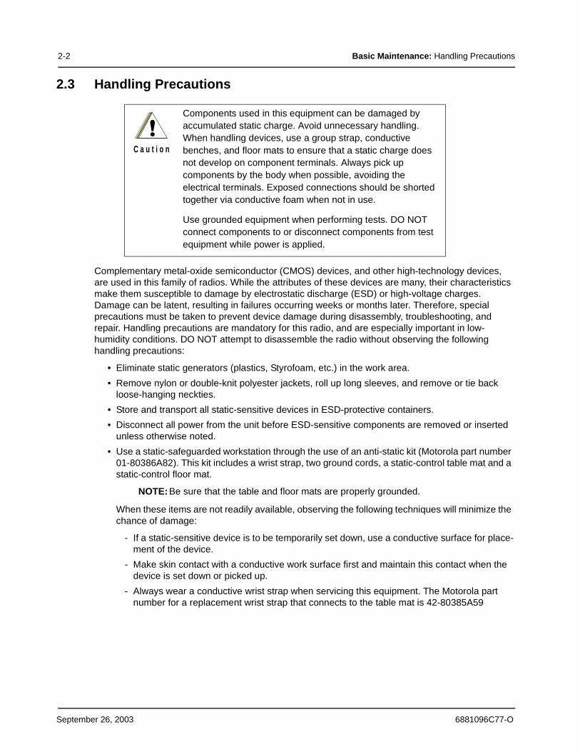
Complementary metal-oxide semiconductor (CMOS) devices, and other high-technology devices, are used in this family of radios. While the attributes of these devices are many, their characteristics make them susceptible to damage by electrostatic discharge (ESD) or high-voltage charges. Damage can be latent, resulting in failures occurring weeks or months later. Therefore, special precautions must be taken to prevent device damage during disassembly, troubleshooting, and repair. Handling precautions are mandatory for this radio, and are especially important in low-humidity conditions. DO NOT attempt to disassemble the radio without observing the following handling precautions:
• Eliminate static generators (plastics, Styrofoam, etc.) in the work area.
• Remove nylon or double-knit polyester jackets, roll up long sleeves, and remove or tie back loose-hanging neckties.
• Store and transport all static-sensitive devices in ESD-protective containers.
• Disconnect all power from the unit before ESD-sensitive components are removed or inserted unless otherwise noted.
• Use a static-safeguarded workstation through the use of an anti-static kit (Motorola part number 01-80386A82). This kit includes a wrist strap, two ground cords, a static-control table mat and a static-control floor mat.
NOTE:Be sure that the table and floor mats are properly grounded.
When these items are not readily available, observing the following techniques will minimize the chance of damage:
- If a static-sensitive device is to be temporarily set down, use a conductive surface for place-ment of the device.
- Make skin contact with a conductive work surface first and maintain this contact when the device is set down or picked up.
- Always wear a conductive wrist strap when servicing this equipment. The Motorola part number for a replacement wrist strap that connects to the table mat is 42-80385A59
Components used in this equipment can be damaged by accumulated static charge. Avoid unnecessary handling. When handling devices, use a group strap, conductive benches, and floor mats to ensure that a static charge does not develop on component terminals. Always pick up components by the body when possible, avoiding the electrical terminals. Exposed connections should be shorted together via conductive foam when not in use.
Use grounded equipment when performing tests. DO NOT connect components to or disconnect components from test equipment while power is applied.
!C a u t i o n
September 26, 2003 6881096C77-O

Chapter 3 Theory of Operation
This chapter describes the operational theory of the control heads for the W3, W4, W5, W7, and W9 radio models. It includes vehicular interface port (VIP) information.
3.1 W3 Control HeadThe W3 Hand-Held Control Head (HHCH) contains the U3 microcomputer, which runs on a 4 MHz clock and performs the following basic functions:
• SB9600 data encode and decode for communication to host radio.
• Liquid-crystal display (LCD) drive comprising two rows of 14 dot-matrix characters plus 10 annunciators.
• Scans a 22-key keypad.
• Scans three side keys and three top keys.
• Determines what type of radio is connected from the bus data and selects either portable or mobile/vehicle adaptor (VA) modes.
• Scans the PTT switch.
• Provides display drive and programmable adjustment for display contrast.
• Provides display and keypad backlight control.
• Activates the red PTT LED and yellow status LED as required.
• Provides remote keying of the microphone via the SB9600 serial bus as required.
• Detects off-hook/on-hook conditions in mobile/VA mode.
• Provides SPI serial communications to U8 for serial-to-parallel output expansion, U12 for parallel-to-serial input compression, U14 for analog-to-serial input compression, and option connector J2.
3.1.1 SB9600 Serial Bus Interface
The serial interface circuit, comprising transistors Q1, Q2, and Q8, and comparator U2, provides an interface between the microphone/message and a host radio for two-way SB9600 serial bus communications. This is necessary to control the radio from the HHCH and have radio status messages displayed on the HHCH. The interface circuit performs the following functions:
• Buffering of the input and output data by Q1 and U2 to improve isolation and drive capability.
• Conversion of balanced to unbalanced SB9600 data input to SB96 bus interface by Q1, U2.
• Bidirectional busy control through U3-20, -21, and -41 to J 1-3. U320 and -21 are paralleled to provide increased drive capability.
3.1.2 Display Circuit
The display is a liquid-crystal display (LCD) and comprises two rows of 14 dot-matrix characters and 10 annunciators. The display circuit consists of sections involving character generation, backplane drive, negative voltage generation, temperature compensation, and contrast control. A 200 kHz clock is derived from U4-25, which also supplies U14.
3-2 Theory of Operation: W3 Control Head
Operation of the circuit is complex; a brief description is detailed below:
• Display data exits U3-5/12 as eight bits of parallel data. This data addresses a character look-up table in LCD driver/controller U4. This provides the relevant segment output data from U4, as well as LCD drivers U5, U6, and U7, to activate the relevant display dots that form the characters as defined in the look-up table.
• The LCD is multiplexed with eight backplanes that are driven separately by U4-47 to -54. Each backplane is driven sequentially, one after the other, by a stepped a.c. voltage of between approximately -2 volts and +5 volts. LCD dots are displayed when a maximum or minimum of one of the backplane drives coincides with a minimum or maximum, respectively, of the relevant segment drive voltage.
• Negative voltage generation necessary for correct operation of the display is derived from a timed clock output from U3-38. This is fed to a voltage doubler comprising C21, C22, and D30. The d.c. output of the doubler is fed to voltage divider R16 to R20. This divider provides evenly spaced voltage increments from approximately -2 volts to +5 volts, which are then fed to U4, U5, U6, and U7 to form the stepped backplane and segment drive voltages.
• Temperature compensation is provided by U3 and U14 in conjunction with D32. This diode provides a temperature-dependent voltage to analog input pin 1 of A/D converter U14. This is sent as serial data input to U3-34, where it is compared to a reference in U3. The amount of deviation from this reference determines the duty cycle of the output drive voltage from U3-38. This results in a change to the drive voltage across C22, which is fed to analog input pin 6 of U14 via voltage divider R26 and R2, which is then fed to U3 as serial data. U3 checks this voltage for accuracy, using the temperature-dependent voltage at U14-1 as a reference, and corrects the drive duty cycle accordingly.
• Contrast control is achieved by adjusting the display drive duty cycle U3-38 by either keypad control or radio programming via the SB9600 bus. U3 contains a reference that presets the drive duty cycle to an average value when first connected to a new radio. Adjustment of the contrast setting will set up a new reference, which will be retained by the radio in EEPROM for future use so that the new setting will be retained if the microphone is turned off.
3.1.3 Keypad Side Keys and Top Keys
The HHCH keypad is configured as a matrix of five columns by six rows. The keyboard is scanned by taking each column output low in turn (each one 1 ms) and reading the corresponding row inputs through the data input latch, U10. After all five columns have been scanned, the row data is then decoded to see which keys, if any, are pressed. The HHCH then waits for debounce until the keypad is scanned again. The keypad is scanned every 25 ms. If the same key is still pressed, the key register value is determined from a key table. If the SB9600 serial bus is not busy, a serial-bus "BUTCTL" message transmission is initiated. The same process also applies when a key is released.
3.1.4 Microphone Preamplifier and PTT
PTT is achieved by activating switch S1. This places a ground on the microphone pre-amplifier circuit, comprising Q6 and associated components, and effectively turns it on. Activation of S7 also places a low on U10-6 input, which is passed on to U3 and transmitted as an SB9600 message back to the radio. When this message is received by the radio, (if required) an SB9600 message is sent back to the microphone and detected by U3, and the PTT LED is activated through U8. However, illumination of the PTT LED is under radio control and is therefore dependent upon radio programming. Q7 is also connected across the PTT line. Its purpose is to remotely enable the microphone pre-amplifier through a received SB9600 serial-bus message, as required.
September 26, 2003 6881096C77-O

Theory of Operation: W3 Control Head 3-3
Microphone cartridge M1 contains a capacitive transducer coupled to a FET amplifier. Microphone audio is obtained from the output of MI and fed to Q6-b via C28, which provides either 0dB of gain in portable mode or 20dB in mobile mode, during transmit. This gain change is achieved by the action of Q5, which is turned on in mobile mode only, and bypasses R71. (Note that this gain is with respect to a radio input impedance of 2k.Ω for portables and 600Ω for mobiles.)
3.1.5 On-/Off-Hook Control
The on-/off-hook control circuit comprises U8 and Hall switch U9. This circuit is only active in mobile mode, during which the output at U8-6 and -7 is driven high by U3. This provides supply volts for U9, the output of which still remains in its normally high state, provided that the microphone is off-hook. During the on-hook condition, when the microphone is retained in its hang-up bracket, a magnet in the hang-up bracket activates the Hall switch, which in turn pulls U9-3 low. This is detected by U3, which then sends an appropriate SB9600 message back to the radio. When the microphone is removed from the hang-up bracket, U9-3 returns high, causing U3 to send another SB9600 message back to the radio.
3.1.6 Backlight Circuit
The backlight circuit comprises U3, U15, Q3, Q4, and LEDs D3 to D17. U3 enables the backlights, as required, by placing a low at U3-16. This, in turn, turns on Q3 and Q4, causing the LEDs to turn on. The action of D35 and R34 provides a constant current source for the LEDs over a supply voltage range of 5.5 to 17 volts. U15 provides current balance between the individual pairs of LEDs, and R34 controls the total current to about 60 mA.
3.1.7 Power Supply
The power supply consists of a 5-volt linear regulator, U1, which provides the necessary 5-volt supply for all of the digital circuits. It has a low drop-out voltage to enable operation from an input voltage of about 5 volts up to 17 volts. This regulator also contains internal current-Iimiting protection, which will normally protect against damage from short-circuit faults. In addition, current is supplied directly from the unregulated input to the backlight LEDs for power dissipation reasons.
3.1.8 Status LEDs
D22 is provided as a status LED for programmable radio functions. It is activated by an SB9600 message from the radio which is detected by U3, resulting in a high at U8-2 and -3. In addition, the PTT LED, D21, can provide flashing radio status messages and can also be activated at the same time as D22.
3.1.9 Jumper Selection
The only jumpers that may normally be installed are JU10, JU11, and JU12. When these jumpers are installed, the ground provided is passed on to U3. These jumpers indicate whether a speaker is installed in the unit, the SB9600 serial-bus device address, and single- or dual-control head control, as defined in the table below.
Table 3-1. W3 Jumper Selection
Jumper IN OUT
JU10 Internal Speaker No internal speaker
JU11 SB9600 address = 6 BS9600 address = 5
JU12 Dual control Single control
6881096C77-O September 26, 2003

3-4 Theory of Operation: W4, W5, and W7 Control Heads
3.1.10 Power On/Off
The HHCH has the ability to turn a host radio on or off by activating S6, which then places a momentary logic low on the Mic Hi line. This is detected by appropriate circuitry in the host radio, which then reverses the power on/off state of the radio. Since the microphone power is supplied by a switched Opt B+ line from the radio, the microphone power on/off state follows that of the radio.
3.1.11 Miscellaneous Functions
If TP1 contacts are momentarily shorted or certain key combinations are pressed simultaneously, the HHCH is placed in its test mode to carry out various diagnostic checks.
Transient protection diodes D24, D25, D37, D38, and D39 provide electrostatic transient protection for sensitive components within the HHCH by preventing voltages from going outside the specified ranges for these components.
3.2 W4, W5, and W7 Control HeadsThe following pages describe the operational theory of the components of the W4, W5, and W7 control heads. Refer to Figure 3-1 for the control-head components.
Figure 3-1. Astro Spectra Control Head Block Diagram
3.2.1 Power Switch/Ignition
For dash-mounted radios, a pushbutton On/Off switch (S1) (or rotary knob on the W4 control head) on the front panel controls power to the radio and accessories. In addition to this switch, you can wire the vehicle’s ignition and add or remove control-head jumpers to further control radio operation.
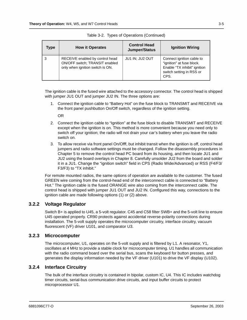
Table 3-2. Types of Operations
Type How it OperatesControl Head
Jumper/StatusIgnition Wiring
1 RECEIVE and TRANSMIT enabled via control head ON/OFF switch (ignition has no effect).
JU1OUT; JU2/IN Connect ignition cable to “Battery Hot” at fuse block.
2 RECEIVE and TRANSMIT enabled only when ignition switch is ON.
JU1/OUT; JU2/IN Connect ignition cable to “Ignition” at fuse block.
VOLTAGECONVERTERCIRCUITRY
5 VOLTREGULATOR
U45
(U3, Q50, T60)
A+/IGN
13.8V 37 VDC
+5 VDC
JU1
JU2
1 2
1 2
A+
IGNITION
U101
VF DRIVERIC
VACUUMFLUORESCENT
DISPLAY
U102
34 VDC
2.5 VAC
VIP OUTPUTS
U1
U4
MICRO-COMPUTER
INTERFACEAND
WATCHDOGTIMER IC
SERIAL DATA BUS
VIP INPUTS
IGNITION SENSE
PTT SENSEHUB SENSE
BACKLIGHTLEDS
1
2
4.0 MHzY1
September 26, 2003 6881096C77-O
Theory of Operation: W4, W5, and W7 Control Heads 3-5
The ignition cable is the fused wire attached to the accessory connector. The control head is shipped with jumper JU1 OUT and jumper JU2 IN. The three options are:
1. Connect the ignition cable to “Battery Hot” on the fuse block to TRANSMIT and RECEIVE via the front panel pushbutton On/Off switch, regardless of the ignition setting.
OR
2. Connect the ignition cable to “Ignition” at the fuse block to disable TRANSMIT and RECEIVE except when the ignition is on. This method is more convenient because you need only to switch off your ignition; the radio will not drain your car’s battery when you leave the radio switch on.
3. To allow receive via front panel On/Offf, but inhibit transit when the ignition is off, control head jumpers and radio software settings must be changed. Follow the disassembly procedures in Chapter 5 to remove the control head PC board from its housing, and then locate JU1 and JU2 using the board overlays in Chapter 8. Carefully unsolder JU2 from the board and solder it in a JU1. Change the “ignition switch” field in CPS (Radio Wide/Advanced) or RSS (F4/F3/F3/F3) to “TX inhibit.”
For remote mounted radios, the same options of operation are available to the customer. The fused GREEN wire coming from the control-head end of the interconnect cable is connected to “Battery Hot.” The ignition cable is the fused ORANGE wire also coming from the interconnect cable. The control head is shipped with jumper JU1 OUT and JU2 IN. Configured this way, connections to the ignition cable are made following options (1) or (2) above.
3.2.2 Voltage Regulator
Switch B+ is applied to U45, a 5-volt regulator. C45 and C58 filter SWB+ and the 5-volt line to ensure U45 operated properly. CR90 protects against accidental reverse-polarity connections during installation. The 5-volt supply operates the microcomputer circuitry, interface circuitry, vacuum fluorescent (VF) driver U101, and comparator U3.
3.2.3 Microcomputer
The microcomputer, U1, operates on the 5-volt supply and is filtered by L1. A resonator, Y1, oscillates at 4 MHz to provide a stable clock for microcomputer timing. U1 handles all communication with the radio command board over the serial bus, scans the keyboard for button presses, and generates the display information needed by the VF driver (U101) to drive the VF display (U102).
3.2.4 Interface Circuitry
The bulk of the interface circuitry is contained in bipolar, custom IC, U4. This IC includes watchdog timer circuits, serial-bus communication drive circuits, and input buffer circuits to protect microprocessor U1.
3 RECEIVE enabled by control head ON/OFF switch; TRANSIT enabled only when ignition switch is ON.
JU1 IN; JU2 OUT Connect ignition cable to “ignition” at fuse block. Enable “TX inhibit” ignition switch setting in RSS or CPS.
Table 3-2. Types of Operations (Continued)
Type How it OperatesControl Head
Jumper/StatusIgnition Wiring
6881096C77-O September 26, 2003

3-6 Theory of Operation: W4, W5, and W7 Control Heads
3.2.5 Reset
On initial power-up, the RESET line to U1-1 is held low by U4 for approximately 120 milliseconds before going high. This resets U1 and starts it operating properly. Then, a pulse train generated at U1-38 sends tickle pulses to the watchdog timer circuitry in U4 and sends a STROBE signal to the VF display driver, U101. Capacitor C6 charges to about 3.3 volts and triggers a reset as described above. Any time a reset occurs, U4-9 goes high, causing radio circuitry in the command board to also reset. Should radio circuitry initiate the reset, pin 23 of the control unit PC board connector is forced high, triggering the same events described above. The control head can reset the radio command board, and vice-versa, via the reset line. See Table 3-3.
3.2.6 Bus Busy
The control head prepares to send data on the serial bus when U-15 (BUSY OUT) goes low, causing U4-10 to go high. This signals the radio command board that the control head has data to send. U4-11 (BUSY IN) goes low whenever U4-10 goes high. This informs the control-head microcomputer that the serial bus is in use. See Table 3-3.
3.2.7 Serial Bus Data
See Table 3-3 for Serial Data Bus Logic. Two lines, BUS+ and BUS-, send data between the control head and the radio command board. Under the normal condition of inactivity, BUS+ is high and BUS- is low. This is the “inactive state” on the serial bus. When the two lines invert (BUS+ goes low, BUS- goes high), the serial bus is in the “active state.”
The control head uses the TX DATA line (U1-33) to send data over the serial bus. When TX DATA goes low, the bus is placed in the active state by U4; when TX DATA goes high, the bus returns to the inactive state.
Data is sent to the microcomputer on the RX DATA line (U1-32). Whenever the serial bus is in the active state, RX DATA is low. An inactive state on the bus causes RX DATA to go high.
Table 3-3. Serial Data Bus Logic
Data LineNo Bus Activity
(NormalReceiving Data)
Bus Activity(Sending or
Receiving Data)In Reset*
Busy Low High Low
BUSY IN High Low High
BUSY OUT High Low* High
BUS+ High Low and High High
BUS- Low High and Low Low
TX DATA High Low and High** High
RX DATA High Low and High High
RESET Low Low High
RESET High High Low
* Bus activity will occur immediately after a reset.** Sending only.
September 26, 2003 6881096C77-O
Theory of Operation: W4, W5, and W7 Control Heads 3-7
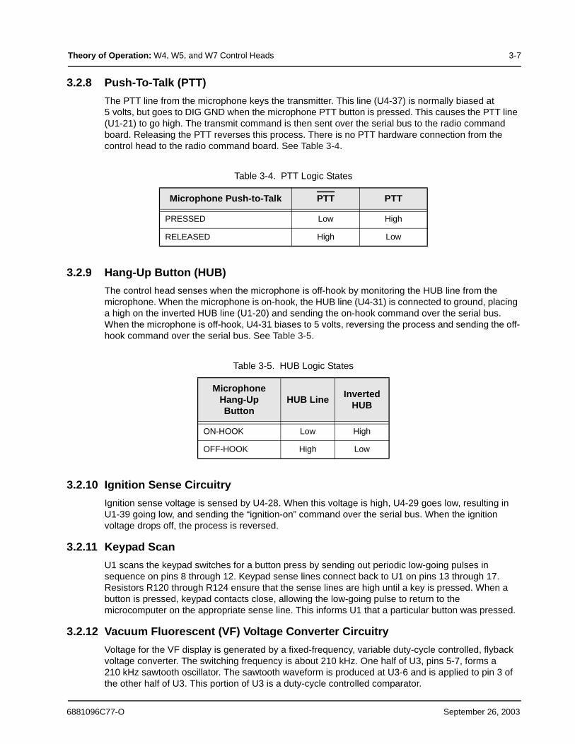
3.2.8 Push-To-Talk (PTT)
The PTT line from the microphone keys the transmitter. This line (U4-37) is normally biased at 5 volts, but goes to DIG GND when the microphone PTT button is pressed. This causes the PTT line (U1-21) to go high. The transmit command is then sent over the serial bus to the radio command board. Releasing the PTT reverses this process. There is no PTT hardware connection from the control head to the radio command board. See Table 3-4.
3.2.9 Hang-Up Button (HUB)
The control head senses when the microphone is off-hook by monitoring the HUB line from the microphone. When the microphone is on-hook, the HUB line (U4-31) is connected to ground, placing a high on the inverted HUB line (U1-20) and sending the on-hook command over the serial bus. When the microphone is off-hook, U4-31 biases to 5 volts, reversing the process and sending the off-hook command over the serial bus. See Table 3-5.
3.2.10 Ignition Sense Circuitry
Ignition sense voltage is sensed by U4-28. When this voltage is high, U4-29 goes low, resulting in U1-39 going low, and sending the “ignition-on” command over the serial bus. When the ignition voltage drops off, the process is reversed.
3.2.11 Keypad Scan
U1 scans the keypad switches for a button press by sending out periodic low-going pulses in sequence on pins 8 through 12. Keypad sense lines connect back to U1 on pins 13 through 17. Resistors R120 through R124 ensure that the sense lines are high until a key is pressed. When a button is pressed, keypad contacts close, allowing the low-going pulse to return to the microcomputer on the appropriate sense line. This informs U1 that a particular button was pressed.
3.2.12 Vacuum Fluorescent (VF) Voltage Converter Circuitry
Voltage for the VF display is generated by a fixed-frequency, variable duty-cycle controlled, flyback voltage converter. The switching frequency is about 210 kHz. One half of U3, pins 5-7, forms a 210 kHz sawtooth oscillator. The sawtooth waveform is produced at U3-6 and is applied to pin 3 of the other half of U3. This portion of U3 is a duty-cycle controlled comparator.
Table 3-4. PTT Logic States
Microphone Push-to-Talk PTT PTT
PRESSED Low High
RELEASED High Low
Table 3-5. HUB Logic States
Microphone Hang-Up Button
HUB LineInverted
HUB
ON-HOOK Low High
OFF-HOOK High Low
6881096C77-O September 26, 2003
3-8 Theory of Operation: W9 Control Head
U1-6 controls the entire voltage converter. During startup, U1-6 pulls to ground, biasing U3-2 to about 1.85 volts via R51 and R52. U3-1 and R61 then begin to switch Q50 on and off at a 210 kHz rate. This allows current to flow through T60, building a magnetic field, then collapsing it. When the field collapses, the back EMF (flyback) forward biases CR51 and charges C52 (after a few cycles) to about 37 volts, causing zener diode VR50 to conduct. The high voltage is regulated by the effect that VR50 has on the bias voltage at U3-2. If the high-voltage supply increases, VR50 pulls U3-2 higher in voltage resulting in a decreased duty-cycle for Q50 (the switching frequency remains constant; only the duty-cycle of on-time versus off-time decreases). Less power is up-converted to C52 when the duty cycle decreases; hence, regulation is maintained.
The voltage converter also produces an a.c. filament voltage for the VF display across T60 pins 4 and 6. R101 drops this voltage to approximately 2.4 Vrms. This a.c. voltage rides on a positive d.c. offset due to R50, depending on brightness. The positive offset allows a VF display grid to be reverse-biased with respect to the filament when that particular grid is supposed to be shut off. This prevents “character ghosting.” Display dimming is exclusively controlled by multiplexing information sent from U1 to the VF driver IC, U101. Display dimming has no effect on the voltage converter circuitry except in the OFF mode. In this mode, U1-6 goes high, resulting in U3-2 going to +5 volts. This keeps U3-1 low and Q50 turned off. The high-voltage supply drops to about 12 volts and the a.c. filament voltage drops to zero, shutting off the display.
3.2.13 Vacuum Fluorescent Display Driver IC
The VF driver IC, U101, receives data directly from the microcomputer for multiplexing the VF display. All of the grid and anode driver lines from U101 are either at, or about, 34 volts (ON) or ground (OFF).
3.2.14 Vacuum Fluorescent Display
The VF display is an 8-character, 14-segment device. Anodes are the actual phosphorescent segments, and grids are the wire-mesh structures located over each character. Multiplexing allows character generation with a minimum of interconnecting lines between display and driver. Anodes and grids operate at, or about, 34 volts when ON and are at zero when OFF. The filament operates on ac at about 2.4 Vrms, with current flow at 100 mA through the filament. The d.c. current flowing from anodes and grids to the filament and through R50 to ground increases filament voltage by up to 5 Vdc.
3.2.15 Backlight LEDs
Most buttons on the control head are backlit by ten LEDs for easy night-time viewing. In medium and low brightness level settings, U1-19 goes high, turning on Q131 and causing a fixed current to flow through the LEDs.
In the OFF mode and the maximum brightness mode, U1-19 goes low, turning off Q131 and the LEDs. Microprocessor U1 does not duty-cycle change the brightness level of the backlighting LEDs.
3.3 W9 Control HeadThe W9 control head has solid-state microprocessor circuitry that operates the standard and optional features built into the system. The control-head design allows installation in even the smallest of down-sized vehicles.
3.3.1 Display
The control head has an 11-character alphanumeric VF display for indicating the following:
• Zone/Mode names
• Squelch level
September 26, 2003 6881096C77-O

Theory of Operation: W9 Control Head 3-9
• Volume level
• Status codes
• Message codes
• Telephone numbers
• Identification numbers
• Alarm displays
• Option status
3.3.2 W9 Controls and Indicators
The W9 control head 12-button keypad contains traditional alphanumeric keys. These keys double as function keys for options. Six ON/OFF option buttons and indicator lights above the display window tell whether these options are on or off. All buttons are backlit to allow operation in low-light conditions.
Other indicators include BUSY, XMIT, Pri, and Non-Pri. The BUSY indicator lights when activity is detected on the channel. The XMIT (transmit) indicator lights when you are transmitting. The Non-Pri (non-priority) or Pri (priority) indicators light when activity occurs during scanning. If the detected activity is in the non-priority mode, the Non-Pri indicator lights. If the activity is in the priority mode, the Pri indicator lights (steady on for second priority mode, and flashing for first priority mode).
3.3.3 Control Board
NOTE: Refer to the W9 control head foldout block diagram and schematic diagram for the following discussion.
The control board's microprocessor unit (MPU) communicates on the serial bus, receives and interprets keypad data, and controls the volume. The MPU (U2) sends data to a driver to control the display and sends data to turn the LEDs on or off. The control board has a watchdog timer that senses the need for a system reset. The vehicle interface ports are also controlled on this board.
3.3.3.1 Microprocessor
The MPU operates in expanded bus mode with internal Read-Only Memory (ROM) active. The clock frequency is 7.9488 MHz, which results in an internal operating frequency of 1987 kHz. The limited number of I/O ports is augmented by using a serial-to-parallel shift register (U6) to scan the keypad and to switch the VIP drivers Q71, Q72, and Q73.
3.3.3.2 Watchdog Timer
The watchdog timer is on the serial input/output integrated circuit (SIOIC) U4. On system power-up, capacitor C6 pulls U4, pin 43, high while the RESET output at pin 4 goes low, and the microprocessor resets.
As C6 charges, the voltage on U4, pin 43, drops, causing the output to go high and the microprocessor to start operating. At this point, the bias on U4, pin 43, shifts toward positive, causing the voltage to begin to rise, eventually causing another reset cycle. A high on U4, pin 9, (RESET input) also initiates a reset.
When the microprocessor operates correctly, the microprocessor sends "tickle" pulses to U4-2. These pulses tickle the watchdog timer and keep the voltage on U4, pin 43, low enough to prevent reset. If the tickle pulses stop for more than 250 ms, the reset cycle repeats.
The watchdog timer can be disabled by shorting U4, pin 43, to ground.
6881096C77-O September 26, 2003

3-10 Theory of Operation: W9 Control Head
3.3.3.3 Bus Transceiver
The serial bus transceiver is on SIOIC U4. The timer on SIOIC U4, pins 10, 16, and 17, connects to the external bus. Pins 11, 13, 19, and 20 connect to MPO 2. These pins act as a serial-communication buffer.
3.3.3.4 Vacuum Fluorescent Voltage Converter
Voltage for the vacuum fluorescent (VF) display filaments is generated by a fixed-frequency, variable-duty-cycle-driven, flyback voltage converter. Dual Comparator U3B, with resistors R56 through R60, form a triangle-wave generator that has an output swing between 1.5 and 3.2 volts at a frequency of 160 kHz. The output of this triangle goes to U3A-3, where it is compared to a feedback signal on U3A-2. The d.c. feedback signal comes from the voltage converter output through diode CR51 and is regulated by VR50 to 43 volts. The U3A output voltage increases or decreases as its input voltage rises or falls. Consequently, the duty cycle seen at the gate of MOSFET transistor Q50 varies inversely with the triangle output voltage. The output of Q50, varying at 160 kHz, is applied to the primary of transformer T60, pins 1 and 3. The secondary of T60, pins 4 and 6, supplies 3.5 Vac for the VF display (U102) filaments.
3.3.3.5 Vehicle Interface Ports
The control-head connector, P103, provides connections for three vehicle interface port (VIP) inputs and three VIP outputs.
The three VIP inputs enter the control head at P103, pins 4, 3, and 37. Zener diodes YR10, YR9, and YR8 limit the input voltages to 15 volts. VIP input 2 can be strapped through jumper JU11 to provide various control functions connected to P103, pins 41, 43, and 44. The three inputs are connected to SIOIC U4 at pins 25, 22, and 35. The input signals are buffered in U4 and are output on pins 24, 21, and 36. From U4, the signals are fed through 10K resistors R44, R14, and R15 to the MPU, U2. The MPU directs the signals as required by programming.
Programmable switches on the control head are connected through J101, pins 11, 10, 9, 8, and 7 (KRl through KRS, respectively) to CPU U2, pins 49, 44, 46, 48, and 50. The other contacts of the switches are connected through J101, pins 14, 15, 16, 17, and 19 (KSl through KSS), to CMOS shift register U6, pins 4, 5, 6, 7, and 14.
Shift register U6 outputs, pins 13, 12, and 11, go to Darlington transistors Q71, Q72, and Q73. These three transistors drive the VIP outputs (up to 300 mA each) through control-head connector PI03, pins 2, 1, and 34. Primarily, these transistors control external relays. VIP outputs 1 and 2 are connected to jumpers JU12 and JU13 to provide control functions connected to P103, pins 28 and 29. VIP output 1 can also be connected through JU22 to MIC-PTT, pin 24.
3.3.3.6 Power Supply
The +5-volt power supply U46 is a three-terminal regulator IC that regulates the 12-volt SWB+ down to +5 volts for the digital logic circuits. The regulated +5 volts enters the control-head PC board through connector J101, pin 4.
3.3.3.7 Ignition Sense Circuits
SIOIC U4 senses the vehicle ignition’s state through its pin 28, disabling transmit when the ignition is off. For negative-ground systems, the orange lead is typically connected to +l2 volts. For more information, see the cable kit section in the Detailed Service Manual 68P80102W61.
NOTE: Q40 supplies an inverting path for positive-ground ignition service.
September 26, 2003 6881096C77-O

Theory of Operation: W9 Control Head 3-11
3.3.3.8 EEPROM Write-Protect Circuit
Transistors Q161, Q162, and associated circuitry guard against inadvertently writing into the EEPROM U5 by inhibiting the Write Enable input. The circuitry guarantees the EEPROM is protected during reset and when shift register U6 is not in the proper programming state.
3.3.4 Display Board
The display board contains the main operator interface points of the system, including the vacuum fluorescent display, the status indicator LEDs, and the user keypad.
NOTE: Refer to the foldout schematic diagram of the display board for this discussion.
3.3.4.1 VF Display
The (VF) display is an 11-digit, 14-segment display that needs two separate voltages to operate, The anode and grids use +43 volts to accelerate electrons from the cathode, and the filament uses 3.5 vac at 80 mA. These voltages are obtained from the VF voltage converter on the controller board.
3.3.4.2 VF Display Driver
VF display driver U101 receives 14-segment display data, digit enable data, and indicator state data from the microprocessor on the controller circuit board. This data is clocked using CLOCK (pin 23) and DATA-IN (pin 43) lines, then framed using LATCH-ENABLE (pin 24) and STROBE (pin 21) to control brightness. The 32-bit data frame is updated every millisecond so that a coherent display is maintained and totally updated every 11 ms.
3.3.4.3 Status LEDs
Status LEDs CR111 through CR120 are driven by the display driver as though they were decimal points on the VF display. Level-shifting transistors are required for this since the display driver uses 43 volts for control signals.
3.3.4.4 Backlight LEDs
The same signal (VF-CONTROL) that turns the VF voltage converter on and off also operates the backlight LEDs. Transistor Q134 supplies base current to the individual driver transistors. The driver transistors act as current sources to the LEDs. Backlight LEDs CR131 through CR134 are connected to thermistor RT133 via Q132. This circuit allows more current to flow through these LEDs at room temperature and reduces current as the temperature rises.
3.3.5 Default Jumper Settings
The factory installs jumpers in each control head according to customer-ordered options. See Table 3-6 for the standard jumper configurations. See the diagrams on the foldout pages for other configurations.
Table 3-6. Standard Jumper Configurations
Jumper Number Normally
JU1 IN
JU2 OUT
JU3 IN
JU4 OUT
6881096C77-O September 26, 2003

3-12 Theory of Operation: Vehicle Interface Port (VIP)
3.4 Vehicle Interface Port (VIP)The vehicle interface port (VIP) allows the control head to control outside circuits in the vehicle and to receive inputs from outside the control head. This results in greater flexibility and ease of installation when interfacing to other systems in the vehicle. There are up to three VIP outputs that can be used for relay control. There are also up to three VIP inputs that can accept input from switches, etc.
3.4.1 W4, W5, and W7 Control Heads
The VIP outputs are controlled by microcomputer U1 pins 26, 27, and 28. A high level causes the associated transistors Q71-73 to conduct up to 300 mA of current to ground. Primarily, these transistors control external relays. The relay coil is connected between the VIP output pin and SWB+. See the installation manual for connection details.
The VIP input lines connect to U4, pins 22, 25, and 35. U4 acts as an inverting stage, passing the VIP input signals to U1, pins 29-31, to be read by the microcomputer. VIP inputs normally connect to ground via a normally open or normally closed switch.
3.4.1.1 VIP Output Connections
3.4.1.1.1 Dash-Mount Installations
Two VIP outputs are available in dash-mount installations. VIP OUT 1 is on pin 12 of the rear accessory connector; VIP OUT 2 is on pin 3. These connections are used to control relays. Connect one terminal of the relay coil to SWB+ (Rear Accessory Connector pin 4). Connect the other relay coil terminal to one of the VIP outputs. See the installation manual for the horn and lights connection.
JU5 IN
JU7 IN
JU8 OUT
JU9 OUT
JU10 OUT
JU11 OUT
JU12 OUT
JU13 OUT
JU16 OUT
JU17 OUT
JU18 IN
JU19 IN
JU20 IN
JU21 OUT
JU22 OUT
Table 3-6. Standard Jumper Configurations (Continued)
Jumper Number Normally
September 26, 2003 6881096C77-O

Theory of Operation: Vehicle Interface Port (VIP) 3-13
Figure 3-2. Cabling Interconnect Diagram for Dash Mount
3.4.1.1.2 Remote-Mount Installations
VIP outputs function exactly the same in remote-mount installations as the dash mount. However, three VIP outputs are available at the remote-mount accessory cable connector. VIP OUT 1 is on pin 12, VIP OUT 2 is on pin 3, and VIP OUT 3 is on pin 15.
Figure 3-3. Cabling Interconnect Diagram for Remote Mount
3.4.1.2 VIP Input Connections (Remote-Mount Only)
Three VIP input lines are also available in remote-mount installations. VIP IN 1 is on pin 14, VIP IN 2 is on pin 10, and VIP 3 is on pin 9. These connections are used to accept input from switches or other circuits in the vehicle. The VIPs are biased at about 5 volts, and to be activated the inputs are switched to ground. Normally, a switch is connected from a VIP input line to ground. The switch can be normally open or normally closed, depending on VIP programming and the particular function being performed.
RADIO COMPARTMENT = OPERATOR COMPARTMENT VEHICLE BATTERYCOMPARTMENT
A good chassis connection via the black primary power cable is essential for radio operation and to prevent damage to the radio and cable kit. Connection to the vehicle frame is desirable.
VEHICLE BATTERY
15A OR 20AFUSE
PART OFVEHICLEWIRING
VEHICLEIGNITION SWITCH
ON/ACC
GROMMET
RADIO POWER CABLE(RED/BATTERY HOT)
RADIO IGNITIONCABLE (thin RED)
SPEAKER
3A OR 4A FUSE
MICROPHONE
RADIO POWER CABLE (BLK/GROUND)
RADIO
(-)(+)
CAUTION
MAEPF-27646-O
Rear connector
CH SEE NOTE
NOTE:Caution: if you choose to connect the radio’s IGNITION line directly to the car’s battery, excess use of the radio when the car’s ignition is not running (i.e. alternator running) could result in a slow discharge of the car’s battery. This configuration allows the radio to operate with the car’s ignition switch ON or OFF.
If the radio’s IGNITION line is wired to the car’s ignition switch, the radio will only function when the car’s ignition switch is turned ON.
RADIO COMPARTMENT OPERATOR COMPARTMENT VEHICLE BATTERYCOMPARTMENT
A good chassis connection viathe black primary power cableis essential for radio operationand to prevent damage to theradio and cable kit. Connectionto the vehicle frame is desirable.
VEHICLE BATTERY
15A OR 20AFUSE
PART OFVEHICLEWIRING
VEHICLEIGNITION SWITCH
ON/ACC
GROMMET
GROMMETSEE NOTE
RADIO POWER CABLE(RED/BATTERY HOT)
RECEIVERCONTROL
CABLE (GRN)
RADIO CONTROLCABLE (BLK/MULTI-
CONDUCTOR)
SPEAKER
TRANSMITTERCONTROL
CABLE (ORG)
4.0A FUSE
MICROPHONE
VIP
MIC
RADIO (ORG)
(GRN)
RADIOPOWER CABLE(BLK/GROUND)
RADIO (-)(+)
CAUTION
NOTE:The orange and green power cables connect to either the vehicle battery or the ignition switch. Connect the green cable directly to the battery. The receiver operates when the control head is on. Connect the orange cable to the ignition switch. The transmitter operates only when the ignition switch is on. Alternate connections:Connecting both green and orange cables to the battery allows the control head to turn the receiver and transmitter on or off. Connecting both green and orange cables to the ignition switch allows the ignition switch to turn the receiver and transmitter on or off. (Alternator whine and other noise problems may occur. Isolate the green cable with a Motorola relay, part #59-00813674.)
MAEPF-27616-O
6881096C77-O September 26, 2003

3-14 Theory of Operation: Vehicle Interface Port (VIP)
3.4.2 W9 Control Heads
The VIPs allow the W9 control head to operate outside circuits and to receive inputs from outside the control head. There are three VIP outputs that are used for relay control. There are also three VIP inputs that accept inputs from switches. See the cable kit section for typical connections of VIP input switches and VIP output relays.
3.4.2.1 VIP Output Connections
The VIP output pins are located on the back of the control head below the area labeled VIP. These connections are used to control relays. One end of the relay should be connected to switched B+, while the other side is connected to a software-controlled on/off switch inside the control head. The relay can be normally On or normally Off depending on how the VIP outputs are configured. The control-head connector P103 pins that are connected to the external relays are listed in Table 3-7.
The function of the VIP outputs can be defined by field programming of the control head. Typical applications for VIP outputs are external horn/lights alarm and horn-ring transfer relay control.
3.4.2.2 VIP Input Connections
The VIP input pins are located on the back of the control head below the area labeled VIP. These connections accept inputs from switches. One side of the switch is connected to ground while the other side is connected to a buffered input to the control head. The switch can be normally closed or normally open, depending on how the VIP inputs are configured. The control head provides three VIP input connections. The control-head connector P103 pins that are connected to the external switches are listed in Table 3-8.
The function of the VIP inputs is defined by field programming of the control head. Typical applications for the VIP inputs are for a foot switch or a horn ring switch.
Table 3-7. VIP Output Connections
VIP Output No.
Switched B+ Pin No.
VIP Output Pin No.
Default Function Is Changed with Field Programmer
1 18 2 Horn Relay (Alarm)
2 19 1 Light Relay (Alarm)
3 35 34 Siren-Horn Transfer
Table 3-8. VIP Input Connections
VIP Input No.
Switched B+ Pin No.
VIP Output Pin No.
Default Function Is Changed with Field Programmer
1 20 4 Siren; Horn Ring
2 21 3 Emergency (if option is present)
3 36 37 None
September 26, 2003 6881096C77-O
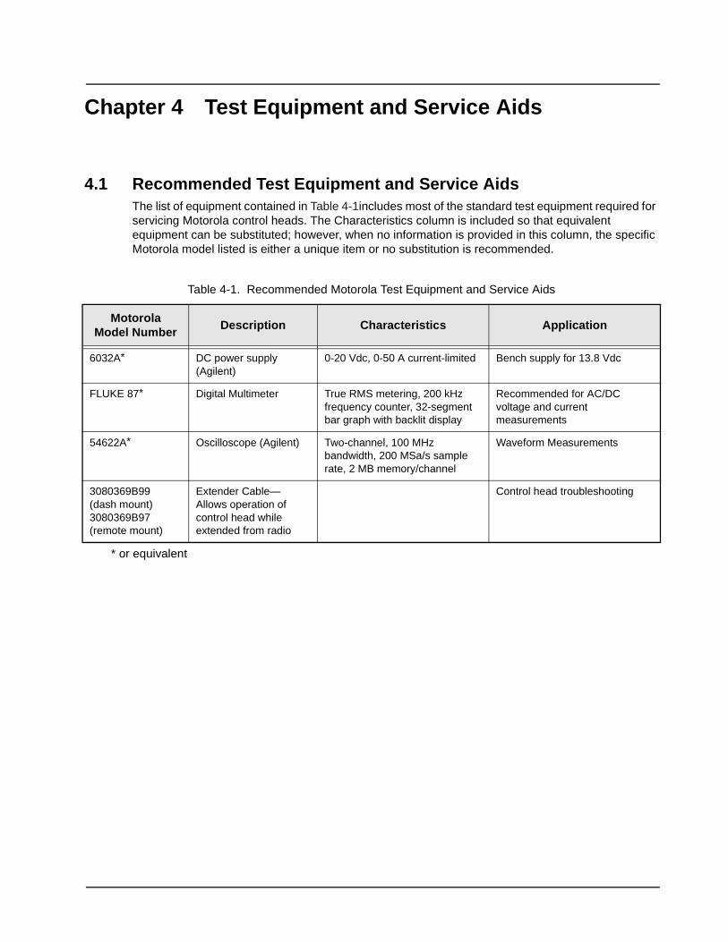
Chapter 4 Test Equipment and Service Aids
4.1 Recommended Test Equipment and Service AidsThe list of equipment contained in Table 4-1includes most of the standard test equipment required for servicing Motorola control heads. The Characteristics column is included so that equivalent equipment can be substituted; however, when no information is provided in this column, the specific Motorola model listed is either a unique item or no substitution is recommended.
Table 4-1. Recommended Motorola Test Equipment and Service Aids
MotorolaModel Number
Description Characteristics Application
6032A* DC power supply (Agilent)
0-20 Vdc, 0-50 A current-limited Bench supply for 13.8 Vdc
FLUKE 87* Digital Multimeter True RMS metering, 200 kHz frequency counter, 32-segment bar graph with backlit display
Recommended for AC/DC voltage and current measurements
54622A* Oscilloscope (Agilent) Two-channel, 100 MHz bandwidth, 200 MSa/s sample rate, 2 MB memory/channel
Waveform Measurements
3080369B99 (dash mount)3080369B97 (remote mount)
Extender Cable—Allows operation of control head while extended from radio
Control head troubleshooting
* or equivalent
4-2 Test Equipment and Service Aids: Recommended Test Equipment and Service Aids
Notes
September 26, 2003 6881096C77-O

Chapter 5 Troubleshooting
This chapter, along with the theory of operation in Chapter 3 and the schematics, overlays, and parts lists in Chapter 8, will aid you in troubleshooting a malfunctioning ASTRO Digital Spectra or Digital Spectra Plus control head. If the board is severely damaged or otherwise non-repairable, refer to the board replacement instructions in the section, “Replacing the Control Head Board” on page 5-7.
NOTE: To access W9 control-head boards for troubleshooting, remove them from the plastic housing using the procedure on page 5-10. To access W4, W5, and W7 control-head boards, use a control-head extender cable and the procedure on page 5-8. (Refer to the chapter, “Recommended Test Equipment and Service Aids” on page 4-1 for the appropriate Motorola test equipment and service aids part numbers.)
5.1 Required Tools and SuppliesTable 5-1lists the tools and supplies needed for basic troubleshooting.
Table 5-1. Required Tools and Supplies
Tools and Supplies
Small, flat-blade screwdriver
2.5 mm hex-key driver
Torx® T8, T10, and T15 drivers
3.0 mm Allen wrench
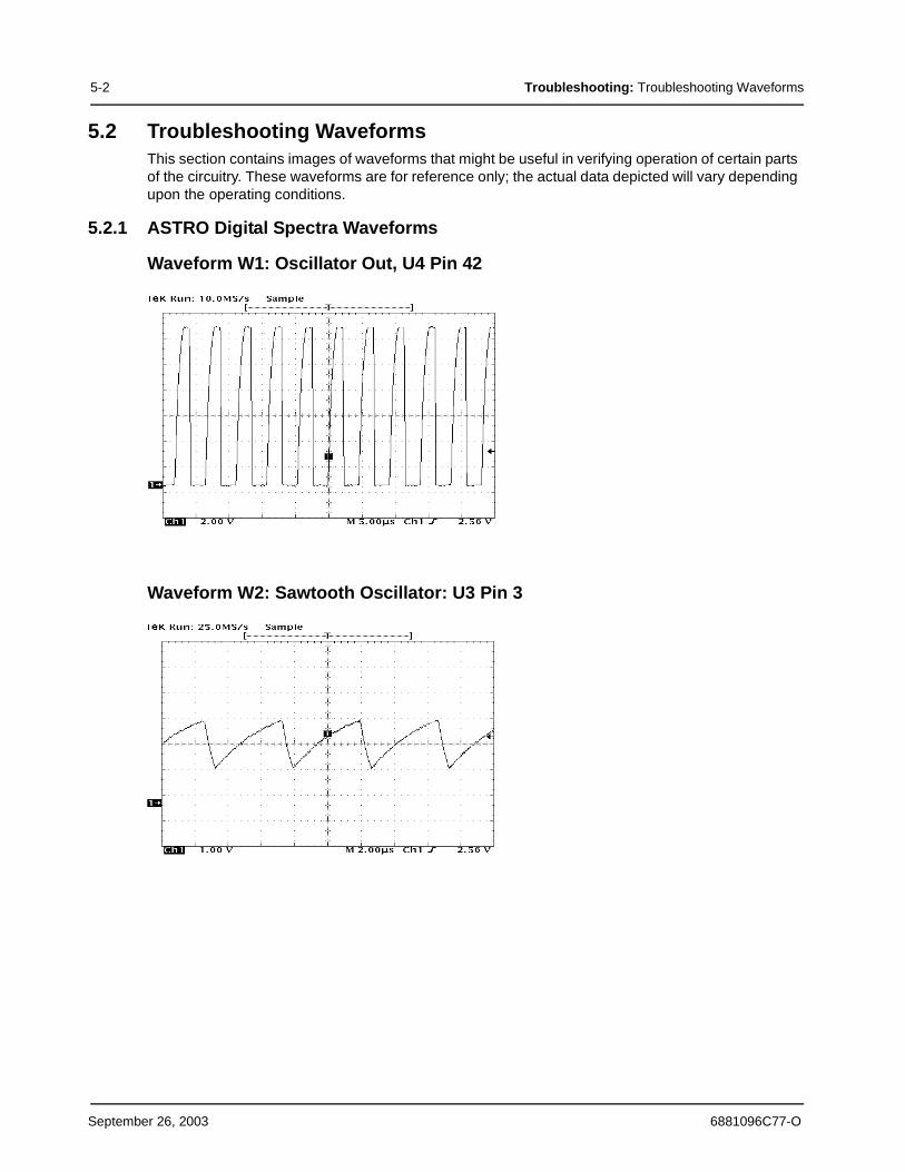
5-2 Troubleshooting: Troubleshooting Waveforms
5.2 Troubleshooting WaveformsThis section contains images of waveforms that might be useful in verifying operation of certain parts of the circuitry. These waveforms are for reference only; the actual data depicted will vary depending upon the operating conditions.
5.2.1 ASTRO Digital Spectra Waveforms
Waveform W1: Oscillator Out, U4 Pin 42
Waveform W2: Sawtooth Oscillator: U3 Pin 3
September 26, 2003 6881096C77-O

Troubleshooting: Troubleshooting Waveforms 5-3
Waveform W3: U3 Output: U3 pin 1 (output to Q50)
Waveform W4: Q50 Drain
6881096C77-O September 26, 2003
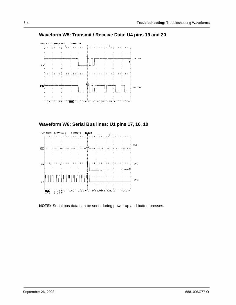
5-4 Troubleshooting: Troubleshooting Waveforms
Waveform W5: Transmit / Receive Data: U4 pins 19 and 20
Waveform W6: Serial Bus lines: U1 pins 17, 16, 10
NOTE: Serial bus data can be seen during power up and button presses.
September 26, 2003 6881096C77-O
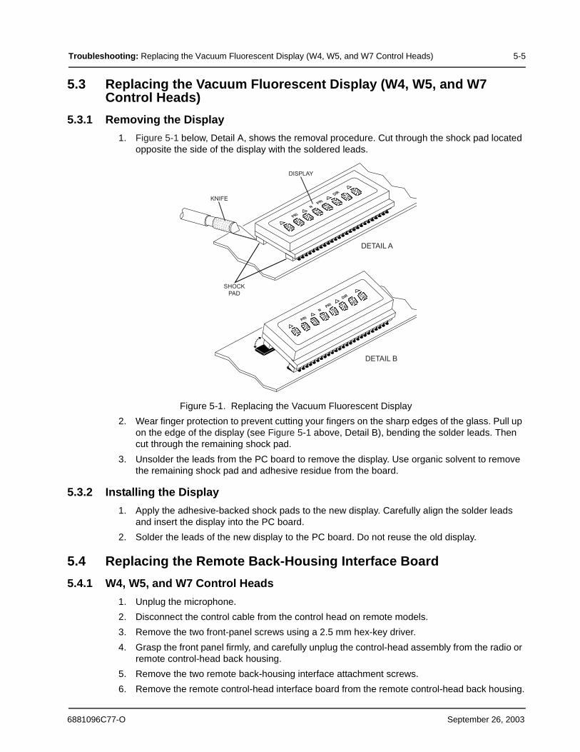
Troubleshooting: Replacing the Vacuum Fluorescent Display (W4, W5, and W7 Control Heads) 5-5
5.3 Replacing the Vacuum Fluorescent Display (W4, W5, and W7 Control Heads)
5.3.1 Removing the Display
1. Figure 5-1 below, Detail A, shows the removal procedure. Cut through the shock pad located opposite the side of the display with the soldered leads.
Figure 5-1. Replacing the Vacuum Fluorescent Display
2. Wear finger protection to prevent cutting your fingers on the sharp edges of the glass. Pull up on the edge of the display (see Figure 5-1 above, Detail B), bending the solder leads. Then cut through the remaining shock pad.
3. Unsolder the leads from the PC board to remove the display. Use organic solvent to remove the remaining shock pad and adhesive residue from the board.
5.3.2 Installing the Display
1. Apply the adhesive-backed shock pads to the new display. Carefully align the solder leads and insert the display into the PC board.
2. Solder the leads of the new display to the PC board. Do not reuse the old display.
5.4 Replacing the Remote Back-Housing Interface Board
5.4.1 W4, W5, and W7 Control Heads
1. Unplug the microphone.
2. Disconnect the control cable from the control head on remote models.
3. Remove the two front-panel screws using a 2.5 mm hex-key driver.
4. Grasp the front panel firmly, and carefully unplug the control-head assembly from the radio or remote control-head back housing.
5. Remove the two remote back-housing interface attachment screws.
6. Remove the remote control-head interface board from the remote control-head back housing.
PRI
PRIN
DIR
PRI
PRI
N
DIR
DETAIL A
DETAIL B
KNIFE
SHOCKPAD
DISPLAY
6881096C77-O September 26, 2003

5-6 Troubleshooting: Replacing the Remote Interconnect Board
7. Before installing a new Interface PC board (P/N 0105950T92), check to ensure that all gaskets are in place. Gasket (P/N 3205197X01) fits the perimeter of the plastic housing on the bottom surface, and is placed against the sealing rim in back housing. Gasket (P/N 3205198X01) fits inside the pin-out area on bottom of plastic housing. Gasket (P/N 3205082E90) O-rings (2) fit into recessed areas around the bottom of the screw clearance holes.
8. Attach the new interface PC board to the back housing with the two screws: torqued to 6-8 in.-lbs.
9. Reassemble the back housing to the front housing with the two screws: torqued to 4-6 in.-lbs.
5.5 Replacing the Remote Interconnect Board
5.5.1 Low-/Mid-Power Radios
1. Remove the two front panel screws using a 2.5 mm hex-key driver.
2. Grasp the front panel firmly, and carefully unplug it from the radio.
3. Remove the three screws that hold the remote interconnect board to the front panel using a Torx T10 driver.
4. Install the new remote interconnect board onto the front panel, and replace the screws. Torque the screws to 6-8 in.-lbs.
5. Reassemble the front panel into the radio and replace the screws.
6. Torque the screws to 4-6 in.-lbs.
5.5.2 High-Power Radios
1. Use a Torx T15 driver to remove the two screws in the radio top cover and then remove the radio top cover.
2. Remove the ribbon cable (38-conductor) from between the command board and the interconnect board by first disconnecting the cable at the command board side and then at the interconnect board.
3. Disengage the retaining wire on the back of the interconnect board at the chassis side.
4. Use the radio key to unlatch the radio handle, and use a Torx T15 driver to remove the two interconnect board screws that are inside the handle.
5. Turn the radio upside down and use a Torx T15 driver to remove the four bottom-cover screws. Remove the bottom cover.
6. Remove the RF-board shield and unplug the coaxial cable that comes up from the other side of the radio. Move the end of the coaxial cable out from behind the interconnect board.
Take care to avoid misalignment of connector pins.
Take care to avoid misalignment of connector pins. Remove the radio top cover to allow visual inspection during connector alignment.
!C a u t i o n
!C a u t i o n
September 26, 2003 6881096C77-O
Troubleshooting: Replacing the Control-Head Board 5-7
7. Pull the retaining wire up into position so that the interconnect board can be slid back away from the front of the radio, and then up and out from the radio chassis.
8. Remove the rubber gasket from the front of the interconnect board by pulling it up and over the D-connectors.
9. Gently pry each of the arms on the interconnect board spacer so that the snap feature on the arms can be slid past the interconnect board.
10. Place the interconnect board spacer onto the new interconnect board, making sure that each arm is aligned in the proper slot and snaps securely into place.
11. Replace the rubber gasket, retaining wire, coaxial cable, bottom cover (torque four screws to 6-8 in.-lbs), and interconnect board screws (torque two screws to 10-12 in.-lbs).
12. Turn the radio top side up and re-insert the ribbon cable (38-conductor) by first connecting the command board side and then the interconnect board side. This cable is connected to two 38-pin connectors. The cable is keyed so that the cable fits only in the correct position.
13. Fold the ribbon cable down flat. Replace the top cover and torque the two screws to 6-8 in.-lbs. These screws are self-tapping and caution should be used so that the screws properly enter the previously cut threads.
5.6 Replacing the Control-Head Board
5.6.1 W3 Control Heads
NOTE: Numbers shown in brackets in the following procedure refer to item numbers in Figure 7-1, “W3 Hand-Held Control Head Exploded View,” on page 7-2, and in Table 7-2, “W3 Hand-Held Control Head Exploded View Parts List,” on page 7-2.
1. Remove the strain-relief boot (part of cable assembly [15]) from the housing assembly [7] by applying downward pressure on the boot and pulling it away from the control head until they are completely separated.
2. Carefully remove the rubber seal (part of cable assembly [15]) from the housing assembly [7] opening.
NOTE:Take care to avoid damaging this seal.
3. Using a small screwdriver, remove the seal support wedge [14] from the control head.
4. Using a small screwdriver to depress the telco lever, remove the telco connector (part of cable assembly [15]) from the control head, and pull the cable assembly away from the housing (like a telephone jack).
5. Remove the rear-cover assembly [2] from the control head.
6. Locate the recesses in the lower portion of the housing on both sides of the rear-cover’s snap features and, prying the snaps until the two parts separate, remove the rear cover from the unit.
7. Remove the two snap retainers [4] from between the circuit board [5] and the housing assembly [7].
8. Disconnect the microphone assembly [8] connector from the circuit board [5].
9. Carefully remove the microphone cable assembly from the keypad [6].
10. Carefully pry the housing’s snap features from the circuit board [5].
NOTE:Be careful to avoid damaging circuit-board components.
There are seven snaps locking the circuit board to the housing. As the snap features are deflected, push the circuit board upward, using the keypad, to release the circuit board from the snap features.
6881096C77-O September 26, 2003

5-8 Troubleshooting: Replacing the Control-Head Board
11. Remove the circuit-board assembly from the housing.
12. Remove the keypad [6] from the housing assembly [7].
5.6.2 W4, W5, and W7 Control Heads
NOTE: For the following procedure, refer to Chapter 7: Exploded Views and Parts Lists, beginning on page 7-1, for the exploded view and associated parts list applicable to the model being disassembled.
1. Unplug the microphone.
2. Remove the two front-panel screws using a 2.5 mm hex-key driver.
3. Disconnect the control cable on remote models.
4. Grasp the front panel firmly, and carefully unplug the control-head assembly from the radio or remote control-head back housing.
5. Lay the control head face down on a clean, flat surface, being careful not to scratch or mar the display.
6. Using a Torx T10 driver, remove the control-head screws:
- W4 Control Head: four screws [callouts 5-8], as shown in Figure 5-2.
The W4 control head has, in addition to the screws, four snap features [callouts 1-4], which are shown in Figure 5-2.
- W5 and W7 Control Heads: seven screws, as shown in Figure 5-3.
Figure 5-2. Model W4 Rotary Control Head Assembly Screw and Snap Sequence
Figure 5-3. Models W5 and W7 Pushbutton Control Head Assembly Screw Sequence
7 158
34 2 6
416
253
7
September 26, 2003 6881096C77-O

Troubleshooting: Replacing the Control-Head Board 5-9
7. Carefully separate the PC board, internal spacer, and elastomer keypad assembly from the front panel.
- On rotary control-head models, care must be taken not to damage the flex circuit when separating the printed circuit board from the front housing. Do not disturb the buttons in the front panel.
- On rotary control-head models, the flex circuit must also be unplugged.
8. On rotary control-head models, desolder the XMIT and BUSY LED before removing the elastomer keypad.
9. Remove the elastomer keypad from the PC board.
NOTE:Before you unsnap the PC board, note that the board slips under a hook on the right and snaps on the left. This will facilitate the assembly.
10. Remove the PC board from the internal spacer. The PC board snaps into and out of the spacer.
11. To reassemble, snap the PC board into the internal spacer. Before you press the elastomer keypad into the board, make sure that the conductive pads in the board and the elastomer keypad are clean and free of any foreign material.
12. On rotary control head models, solder the XMIT and Busy LEDs onto the PC board.
NOTE:On rotary control head models, the flex circuit must be connected to the PC board prior to attaching the PC board to the spacer.
13. Install the PC board internal spacer and elastomer keypad assembly into the front panel. Replace the screws and torque them to 6-8 in.-lbs.
14. Do one of the following:
- For dash-mounted radios, plug the interconnect board into the radio, and then plug in the control-head assembly and fasten it with the two front-panel screws (torqued to 4-6 in.-lbs).
- For remote-mount control heads, replace the front panel into the remote control-head back housing, make sure the gasket is in place, and then torque the screws to 4-6 in.-lbs. Replace any plugs and cables on the rear of the control head.
Take care to avoid misalignment of connector pins. On dash mount radios, remove the radio top cover to allow visual inspection during connector alignment.
!C a u t i o n
6881096C77-O September 26, 2003
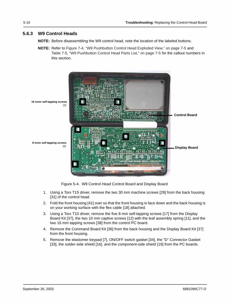
5-10 Troubleshooting: Replacing the Control-Head Board
5.6.3 W9 Control Heads
NOTE: Before disassembling the W9 control head, note the location of the labeled buttons.
NOTE: Refer to Figure 7-4, “W9 Pushbutton Control Head Exploded View,” on page 7-5 and Table 7-5, “W9 Pushbutton Control Head Parts List,” on page 7-5 for the callout numbers in this section.
Figure 5-4. W9 Control Head Control Board and Display Board
1. Using a Torx T15 driver, remove the two 30 mm machine screws [29] from the back housing [31] of the control head.
2. Fold the front housing [41] over so that the front housing is face down and the back housing is on your working surface with the flex cable [18] attached.
3. Using a Torx T10 driver, remove the five 8 mm self-tapping screws [17] from the Display Board Kit [37], the two 10 mm captive screws [12] with the leaf assembly spring [11], and the two 16 mm tapping screws [38] from the control PC board.
4. Remove the Command Board Kit [36] from the back housing and the Display Board Kit [37] from the front housing.
5. Remove the elastomer keypad [7], ON/OFF switch gasket [34], the “D” Connector Gasket [33], the solder-side shield [16], and the component-side shield [19] from the PC boards.
Control Board
Display Board
16 mnm self-tapping screws(2)
8 mnm self-tapping screws(5)
September 26, 2003 6881096C77-O

Troubleshooting: Final Reassembly–W3 Control Head 5-11
6. Install the new PC board with the elastomer keypad, the ON/OFF switch gasket, the “D” Connector Gasket, the “D” Connector O-ring, the solder-side shield, and the component-side shield in the appropriate locations.
7. Reassemble the Command Board Kit [36] into the back housing [31], making sure that the power switch is in the proper location and then replace the two tapping screws [38], torquing them to 6-8 in.-lbs.
8. Reassemble the Display Board Kit [37] into the front housing [41], making sure that the elastomer keypad [7] is in the proper location.
9. Replace the captive screws [12] and the leaf assembly spring [11] in the front housing, and then torque them to 6-8 in.-lbs.
NOTE:Before assembling the leaf assembly spring, ensure that the insulator [10] on the board is present. Also ensure that the leaf assembly spring and captive screws are aligned properly to prevent stripping the front housing screw bosses.
10. Close the assembly by replacing the front housing [41] and the two screws in the back housing [31]. Torque the screws to 6-8 in.-lbs.
5.7 Final Reassembly–W3 Control HeadWhen reassembling the control head, make sure the microphone pins are properly inserted through the elastomeric keypad. Also make sure the elastomeric keypad inserts are secured to the PC board.
NOTE: Numbers shown in parentheses in the following procedure refer to item numbers in Table 7-2, “W3 Hand-Held Control Head Exploded View Parts List,” on page 7-2.
1. To reassemble the housing assembly [7]:
A. Insert the transmit indicator [11] into the housing. Ensure that the top surface of the lightpipe is below the label recess of the housing.
B. Attach the nameplate label [13] to the front of the housing. Ensure that the label is securely attached.
C. Install the PTT actuator [9] into the housing. Ensure that its lip is seated in the grove in the housing.
D. Install the PTT lever [10] and the PTT boot [12] into the housing. Ensure that the lever is seated in its nest and the boot is located properly in the recesses in the housing.
E. Install the keypad [6] into the housing. Ensure that all of the keys are located in the correct openings in the housing.
2. Install the microphone assembly [8] into the keypad. Ensure that the front surface of the cartridge is located up against the keypad membrane.
NOTE:The membrane is the rain seal and is very sensitive to puncture by sharp objects.
3. Connect the microphone cable connector to the mating location on the circuit board [5].
Be careful to not bend the tabs on the shields when removing them and align them carefully when replacing the shields. When working with chips and SOT (small-outline transistor) parts, use extreme caution when heating. Never reuse a chip or SOT part; always replace with the correct Motorola part.
!C a u t i o n
6881096C77-O September 26, 2003
5-12 Troubleshooting: Troubleshooting Charts
4. Install the circuit board [5] into the housing assembly [7] as follows:
A. Hold the housing assembly so that its key openings face downward and its top faces away from you.
B. Pivot the circuit board’s display down under the retention features in the housing and rotate the board downward, ensuring that the board is positioned between the snap features. Ensure that the microphone assembly’s [8] wire passes through the opening in the circuit board.
C. Press downward firmly on the board until the seven snap features lock the board into place.
5. Install the two snap retainers [4] between the circuit board and the side wall of the housing assembly [7], one on each side.
6. Install the main seal [3] onto the rear cover assembly [2], placing the seal under the retainer features around the perimeter of the cover.
7. Install the rear cover assembly [2] onto the housing assembly [7].
Starting at the top of the cover, pivot the cover toward the housing and squeeze the two halves together until the snap features at the lower end of the rear cover engage the housing’s features and snap closed.
8. Insert the cable assembly’s [15] telco connector into the opening in the bottom of the housing, and ensure that it is correctly oriented.
9. Press the telco connector in place until it snaps in (like a phone plug).
10. Place the seal-support wedge [14] into the housing’s opening, orienting it so that its long portion is under the telco connector lever, and then push until it is properly seated.
11. Push the rubber seal (part of the cable assembly [15]) into the housing’s opening and ensure that it is properly seated.
NOTE:This seal must be inserted completely into the housing to ensure the rain seal.
12. Push the strain-relief boot (part of the cable assembly [15]) into the housing and ensure that it is properly seated.
13. Insert the kit label [1] into the recess on the rear cover, and ensure that it is securely attached.
5.8 Troubleshooting ChartsThis section contains detailed troubleshooting flowcharts. These charts should be used as a guide in determining the problem areas. They are not a substitute for knowledge of circuit operation and astute troubleshooting techniques. It is advisable to refer to the related detailed circuit descriptions in the theory section prior to troubleshooting a radio.
September 26, 2003 6881096C77-O
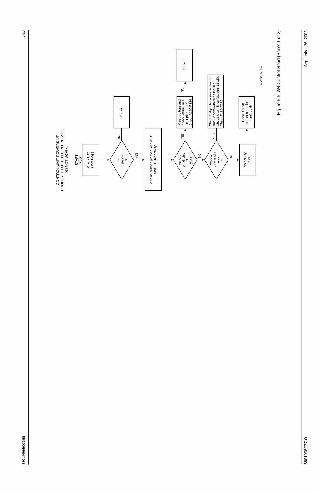
Tro
ub
lesh
oo
tin
g5-
13
6881
096C
77-O
Sep
tem
ber
26, 2
003
Fig
ure
5-5.
W4
Con
trol
Hea
d (S
heet
1 o
f 2)
ST
AR
T
Che
ck U
45(+
5V R
eg.)
Rep
air
Is+
5V O
K?
With
no
butto
ns p
ress
ed, c
heck
U1
pins
8-1
1 fo
r ac
tivity
.
Act
ivity
on a
ll pi
ns?
(8-1
1)
Act
ivity
on o
ne p
inon
ly ?
No
activ
ityat
all
Che
ck U
1 fo
rpr
oper
ope
ratio
nan
d re
pair
Che
ck th
at p
in fo
r a
shor
ted
butto
ncl
osur
e so
mew
here
on
the
line.
Che
ck r
etur
n lin
es (
U1
pins
13-
15).
Che
ck R
120-
R12
2.
Pre
ss b
utto
ns a
ndch
eck
retu
rn li
nes
(U1
pins
13-
17).
Che
ck R
120-
R12
4
Rep
air
MA
EP
F-2
2619
-A
CO
NT
RO
L U
NIT
PO
WE
RS
UP
PR
OP
ER
LY B
UT
BU
TT
ON
PR
ES
SE
SD
O N
OT
WO
RK
.
YE
S
YE
S
NO
YE
S
NO
NO
NO

5-14
Tro
ub
lesh
oo
tin
g
Sep
tem
ber
26, 2
003
6881
096C
77-O
Fig
ure
5-6.
W4
Con
trol
Hea
d (S
heet
2 o
f 2)
A
ACR
50 is
Pro
babl
y O
pen
Che
ckU
101-
1V
olta
ge
IsV
olta
ge33
to 3
9V? Is
Vol
tage
over
40V
? IsV
olta
ge20
to 2
5V? Is
Vol
tage
11 to
14V
?
Cho
ose
the
clos
est v
olta
gera
nge
and
proc
eed
IsR
eset
Lin
eO
K ?
Che
ck U
1: U
4: Y
1 fo
r pr
oper
oper
atio
n. U
1-1
mus
t go
low
mom
enta
rily
afte
rpo
wer
up,
then
sta
y hi
ghto
pro
perly
initi
aliz
e U
1
Rep
air
and
Ret
urn
toS
tart
CR
50 is
prob
ably
ope
nR
emov
e V
FD
ispl
ay
Che
ck T
60pi
ns 1
, 2, 3
cont
inui
ty
Che
ckC
52
Che
ck U
4 an
dca
blin
g fo
r so
urce
of p
robl
em
Rep
air
and
Ret
urn
toS
tart
ST
AR
T
VE
RY
BR
IGH
T D
ISP
LAY
VA
RIE
S W
ITH
SU
PP
LY V
OLT
AG
E
Che
ck V
F D
ispl
ayF
ilam
ent V
olta
ge w
ith a
nA
C v
oltm
eter
bet
wee
n pi
ns1
and
25 o
f VF
Dis
play
. The
volta
ge s
houl
d be
2 to
3 V
rms
Che
ck R
51, R
52,
C51
, C52
and
repa
ir
OK ? Is
C52
OK
?
Pos
sibl
e sa
wto
oth
osci
llato
r pr
oble
mR
emov
e V
F
Dis
play
Obs
erve
wav
efor
mat
U3-
3. C
ompa
rew
ith
Wav
efor
m W
2 in
sec
tion
5.8
Ret
urn
To
Sta
rt
CR
51 is
pro
babl
yop
enR
emov
e V
FD
ispl
ay
Rep
air
and
Ret
urn
toS
tart
Q50
may
hav
ebe
en o
vers
tres
sed
durin
g fa
ilure
Rep
lace
Q50
Che
ck C
R51
,Q
50 a
ndR
epai
r
Ret
urn
To
Sta
rt
Che
ck V
F D
ispl
ayF
ilam
ent
For
Ope
n
Ret
urn
To
Sta
rt
Che
ck R
101,
T60
and
Rep
air
IsF
ilam
ent
Ope
n?Is
Vol
tage
Cor
rect
?
Che
ck R
50an
d T
60pi
ns 4
, 5, 6
fo
r co
ntin
uity
Rem
ove
VF
Dis
play
and
Rep
lace
Ret
urn
To
Sta
rt
OK ?
Che
ck U
101
and
U1
for
prop
erop
erat
ion
Rep
air
and
Ret
urn
toS
tart
Isw
avef
orm
corr
ect
?
Che
ck D
C v
olta
geon
U3-
2. It
sho
uld
be 1
.5 to
2.0
VD
C
Isvo
ltage
corr
ect
?
Che
ck U
3-1
Wav
efor
m W
3in
sec
tion
5.8
Isw
avef
orm
pres
ent
?
Che
ck Q
50 d
rain
.C
ompa
re to
Wav
efor
m W
5 in
sect
ion
5.8
Che
ck U
3, C
54,
R56
-R60
and
Rep
air
Q50
may
hav
e be
enov
erst
ress
eddu
ring
failu
re.
Rep
lace
Q50
Ret
urn
To
Sta
rt
Che
ck R
52,
R51
, C51
and
Rep
air
Che
ck U
3,R
61, Q
50,
and
Rep
air
Q50
may
hav
e be
enov
erst
ress
ed d
urin
gfa
ilure
. Rep
lace
Q50
Ret
urn
To
Sta
rt
Ret
urn
To
Sta
rt
Ret
urn
To
Sta
rt
Isw
avef
orm
pres
ent
?
Che
ck R
61,
Rep
lace
Q50
Che
ck T
60an
d R
epai
r
Q50
may
hav
e be
enov
erst
ress
ed d
urin
gfa
ilure
. Rep
lace
Q50
Tur
n P
ower
on
with
Con
trol
Hea
dco
nnec
ted
to r
adio
Isdi
spla
y at
pro
per
brig
htne
ssle
vel
?
Che
ck fo
r S
WB
+vo
ltage
on
Con
trol
Hea
d P
C B
oard
IsS
WB
+ O
n?
Che
ck U
45(+
5V R
EG
)
Is+
5V O
K?
Che
ck L
50,
R55
Con
tinui
ty
OK ?
Che
ckU
1-6
IsV
olta
geLo
w ?
No
Pro
blem
EN
D
Rep
air
and
Ret
urn
toS
tart
Rep
air
and
Ret
urn
toS
tart
Che
ck R
eset
line
to s
ee if
it is
bein
g he
ld h
igh
by r
adio
m
alfu
nctio
n
A
ST
AR
T
NO
DIS
PLA
Y O
RV
ER
Y D
IM D
ISP
LAY
Che
ck S
W1,
J10
2,P
102
and
Rep
air:
Ret
urn
to S
tart
NO
YE
S
NO
YE
S
YE
S
NO
NO
YE
S
MA
EP
F-22
618-
O
NO
YE
S
NO
YE
S
YE
S
NO
YE
S
NO
NO
YE
S
YE
S
YE
S
YE
S
YE
S
YE
S
NO
NO
NO
NO
NO
NO
YE
S
YE
S
NO
YE
S
NO
YE
S
NO
YE
S
NO
YE
S
NO
IsV
olta
gebe
low
10V
?
Rep
air
and
Ret
urn
toS
tart

Ch
apte
r 6
Rad
io C
on
nec
tors
Thi
s ch
apte
r co
ntai
ns th
e A
ST
RO
Dig
ital S
pect
ra a
nd D
igita
l Spe
ctra
Plu
s co
nnec
tor
loca
tions
.
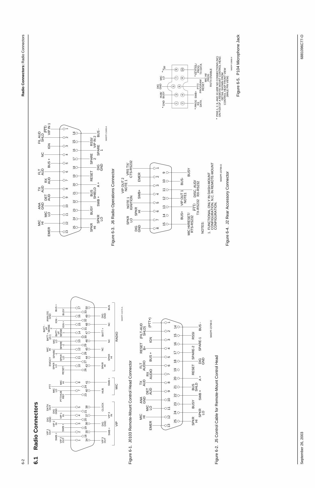
6-2
Rad
io C
on
nec
tors
: R
adio
Con
nect
ors
Sep
tem
ber
26, 2
003
6881
096C
77-O
6.1
Rad
io C
on
nec
tors
Fig
ure
6-1.
J01
03 R
emot
e-M
ount
Con
trol
Hea
d C
onne
ctor
Fig
ure
6-2.
J5
Con
trol
Cab
le fo
r R
emot
e-M
ount
Con
trol
Hea
d
Fig
ure
6-3.
J6
Rad
io O
pera
tions
Con
nect
or
Fig
ure
6-4.
J2
Rea
r A
cces
sory
Con
nect
or
Fig
ure
6-5.
P10
4 M
icro
phon
e Ja
ck
12
34
51
31
21
11
08
71
41
51
61
7
48
49
40
41
34
43
44
35
36
37
38
45
46
47
50
VIP
2O
UT
VIP
1O
UT
VIP
2IN
VIP
1IN
DA
TA
OU
T
MIC
LO
MIC HI
SP
KR
LO
SP
KR
LO
MIC HI
MIC
LO
BA
TT
-V
FS
EN
SE
1IG
N +
AN
ALO
GG
ND
BU
S +
SW
B +
DIG
GN
D
PT
T/H
UB
RE
F
PT
T
RE
SE
T
EM
GC
YB
AT
T +
(A+
)
BA
TT
-V
FS
EN
SE
2
IGN
-
BU
SY
SW
B +
DIG
GN
D
SP
AR
E-1
SP
AR
E-2 29
28
27
26
30
31
32
18
19
20
21
23
24
33
VIP
3O
UT
SW
B +
DIG
G
ND
VIP
3IN
CLO
CK
HU
B
SW
B +
SP
KR
HI
NC
BA
TT
+D
IGG
ND
BU
SS
PK
RH
IN
CN
C
RA
DIO
MIC
VIP
MA
EP
F-2
16
70
-A
EM
ER
MIC HI
AN
AG
ND
TX
AU
DF
LTA
UD
IO(F
ILT
-AU
DS
HLD
)M
ICLO
DE
TA
UD
RX
AU
DIO
BU
S +
IGN
RE
SE
TB
+
BU
SY
SP
KR
LOS
WB
+
SP
KR
HI
DIG
GN
DB
US
-12
34
56
1312
1110
98
7
1415
1617
1819
2021
2223
2425
MA
EP
F-2
3798
-O
(PT
T )
BU
SS
HLD
A +
RE
SE
TS
PA
RE
-2
SP
AR
E-1R
SS
I
EM
ER
MIC HI
AN
AG
ND
TX
AU
DF
LTA
UD
NC
FIL
AU
DS
HLD
MIC
LOD
ET
AU
DR
XA
UD
BU
S +
IGN
PT
T/
VIP
IN 1
SP
KR
HI
BU
SY
BU
SS
HIE
LDR
ES
ET
SP
KR
LOS
WB
+A
+D
IGG
NDS
PA
RE
2S
PA
RE
1
RS
SI/
VIP
IN 2 B
US
-12
34
56
1312
1110
98
7
1415
1617
1819
2021
2223
2425
MA
EP
F-2
1669
-A
DIG
GN
DS
PK
RH
IE
ME
R
SP
KR
LON
OT
E 1
IGN
ITIO
N
VIP
OU
T 2
NO
TE
1
SW
B+
PT
T/
TX
-RS
23
2
BU
SY1
23
45
68
7
910
1112
1314
15
MA
EP
F-2
3799
-O
VR
S T
X/
CT
S-R
S23
2
MIC
HI/R
ES
ET
/R
TS
-RS
232
BU
S+
VIP
OU
T 1
NO
TE
1
DIS
C. A
UD
/R
X-R
S23
2
BU
S-
FU
NC
TIO
NA
L O
NLY
IN D
AS
H-M
OU
NT
CO
NF
IGU
RA
TIO
N. N
.C. I
N R
EM
OT
E-M
OU
NT
CO
NF
IGU
RA
TIO
N.
NO
TE
S:
1.
GN
D
DIG
GN
DM
ICLO
PT
T/
PR
OG
RA
MR
ES
ET
9 10
7 8
5 6
MA
EP
F-2
3800
-A
PR
OG
RX
DA
TA
SW
B+
PIN
S 1
, 2, 9
, AN
D 1
0 A
RE
NO
CO
NN
EC
TIO
NS
(N
C)
ON
P10
4 O
F A
RE
MO
TE
-MO
UN
T C
ON
TR
OL
HE
AD
.D
ET
AIL
SH
OW
N F
RO
MC
ON
TR
OL
HE
AP
FR
ON
T V
IEW
(MA
LE P
IN V
IEW
)
Vpp
1 2
3 4
HU
B/
BU
SY
KE
YF
AIL
/P
RO
GT
X D
AT
A
MIC
HI/
PR
OG
RX
/TX
EN
AB
LE

Rad
io C
on
nec
tors
: R
adio
Con
nect
or L
ocat
ions
6-3
6881
096C
77-O
Sep
tem
ber
26, 2
003
6.2
Rad
io C
on
nec
tor
Lo
cati
on
s
Fig
ure
6-6.
Das
h-M
ount
Rad
io C
onne
ctor
Loc
atio
ns
Fig
ure
6-7.
Rem
ote-
Mou
nt R
adio
Con
nect
or L
ocat
ions
Fig
ure
6-8.
Com
man
d B
oard
Con
nect
or L
ocat
ions
Fig
ure
6-9.
VO
CO
N B
oard
Con
nect
or L
ocat
ions
MA
EP
F-2
4496
-O
0
PW
R
Mod
e
Sca
nP
hon
Sel
Cal
l
Vol
DIM
HO
ME
XM
IT
BU
SY
12
34
56
78
9
0
Sts
Msg
H/L
Mon
Dir
Rcl
Del
DA
SH
-MO
UN
T R
AD
IO
J2A
NT
EN
NA
PW
R
P50
2
P10
4
MA
EP
F-2
4497
-A
0
PW
R
Mod
e
Sca
nP
hon
Sel
Cal
l
Vol
DIM
HO
ME
XM
IT
BU
SY
12
34
56
78
9
0
Sts
Msg
H/L
Mon
Dir
Rcl
Del
J2
J5
P50
6
RE
MO
TE
-MO
UN
TC
ON
TR
OL
HE
AD
RE
MO
TE
-MO
UN
TR
AD
IO
J6
J010
3
P10
4
AN
TE
NN
AP
WR
CO
MM
AN
D B
OA
RD
(VIE
WE
D F
RO
M S
IDE
1)
P5
03
F5
00
U4
50
15
24
19
16
J50
0
25
0 49
12
53
0 P5
01
P5
02
138
29 10
20
19
13 12
14
13
12
11
10
98
3
65
4 217
121
4 13
25
26
VO
CO
N B
OA
RD
(VIE
WE
D F
RO
M S
IDE
2)
49 50
J50
1
25
24
J80
12 1
1 2

6-4
Rad
io C
on
nec
tors
: E
xten
der
Cab
le (
P50
1)
Sep
tem
ber
26, 2
003
6881
096C
77-O
6.3
Ext
end
er C
able
(P
501)
Fig
ure
6-10
. P
501
Ext
ende
r C
able
6.4
Co
ntr
ol-
Hea
d C
ablin
g D
iag
ram
Fig
ure
6-11
. C
ontr
ol-H
ead
Cab
ling
Dia
gram
1517
1913
119
75
31
2123
2527
2931
3335
3739
4143
4547
49
1618
2014
1210
86
42
2224
2628
3032
3436
3840
4244
4648
50
P50
1E
XT
EN
DE
RC
AB
LE(3
0803
70E
06)
(FA
CIN
G T
OW
AR
DC
ON
TR
OL
HE
AD
)
J501
CO
MM
AN
D B
OA
RD
P10
01
SP
AR
E 2
EM
ER
GE
NC
Y
SP
AR
E 1
DIG
GN
D
SW
B+
BU
S +
BU
S -
BU
SY
BU
S S
HIE
LD
RE
SE
T
DE
T A
UD
IO
AN
A G
ND
PT
T
MIC
HI
MIC
LO
SP
KR
HI
SP
KR
LO
A+
RS
SI
RX
AU
DIO
RE
D
VIO
BR
N
BLU
YE
L
WH
T
BLK
BLK
/RE
D
BA
RE
BLK
/OR
G
BLK
/BR
N
SH
IELD
BLK
/GR
N
SH
IELD
BLK
/YE
L
SH
IELD
OR
G
GR
N
CO
NT
RO
L H
EA
D
OR
G
GR
N
NC
NC
MIC
LO
MIC
HI
SW
B+
HU
B
PT
T
PT
T/H
UB
RE
F
SW
B+
SW
B+
SW
B+
DIG
GN
D
DIG
GN
D
DIG
GN
D
(DA
TA
IN)
(ST
RO
BE
)
(CLO
CK
)
(DA
TA
OU
T)
BU
S +
BU
S -
BU
SY
RE
SE
T
DE
T A
UD
IO
AN
A G
ND
PT
T
IGN
+
IGN
-
BA
TT
+
BA
TT
+
BA
TT
-
SP
AR
E 2
BA
TT
-
EM
ER
GE
NC
Y
SP
AR
E 1
BLK
/GR
N
BLK
/OR
G
DIG
GR
D
SW
B+
P5
RA
DIO
15 32 47 30 31 29 14 27 28 49 48 17 50 33 26 45 16 46 12 13 44 11 10 43 7 8 41 40 24 23 18 19 3 20 21 36 4 3 37 2 1 34 38 5
SP
EA
KE
R
17 13 16 18 22 5 14 23 21 19 9 0 1 12 11 25 24 20 15 71 2 3 1 2 3
VIP
IN
VIP
OU
T

Ch
apte
r 7
Exp
lod
ed V
iew
s an
d P
arts
Lis
ts
Thi
s ch
apte
r co
ntai
ns th
e ex
plod
ed v
iew
s an
d as
soci
ated
par
ts li
sts
for
each
of t
he A
ST
RO
Dig
ital S
pect
ra a
nd D
igita
l Spe
ctra
Plu
s co
ntro
l hea
ds. T
able
s co
ntai
ning
pus
hbut
ton
part
s lis
ts a
re a
lso
incl
uded
.
Tabl
e 7-
1. E
xplo
ded
Vie
ws
Fig
#D
escr
ipti
on
Pag
e #
Fig
ure
7-1
W3
Han
d-H
eld
Con
trol
Hea
d E
xplo
ded
Vie
w7-
2
Fig
ure
7-2
W4
Rot
ary
Con
trol
Hea
d E
xplo
ded
Vie
w7-
3
Fig
ure
7-3
W5
and
W7
Pus
hbut
ton
Con
trol
Hea
d E
xplo
ded
Vie
w7-
4
Fig
ure
7-4
W9
Pus
hbut
ton
Con
trol
Hea
d E
xplo
ded
Vie
w7-
5
Fig
ure
7-5
HM
N10
80A
, HM
N10
61A
, HM
N10
79A
Mic
roph
one
Exp
lode
d V
iew
7-6

Sep
tem
ber
26, 2
003
6881
096C
77-O
7-2
Exp
lod
ed V
iew
s an
d P
arts
Lis
ts:
Mod
el W
3 H
and-
Hel
d C
ontr
ol H
ead
Exp
lode
d V
iew
7.1
Mo
del
W3
Han
d-H
eld
Co
ntr
ol H
ead
Exp
lod
ed V
iew
Fig
ure
7-1.
W3
Han
d-H
eld
Con
trol
Hea
d E
xplo
ded
Vie
w
2
1
3
4
5
6
7
8
4 15
14
10
9
1211
13
Tabl
e 7-
2. W
3 H
and-
Hel
d C
ontr
ol H
ead
Exp
lode
d V
iew
Par
ts L
ist
Item
No
.M
oto
rola
Par
t N
o.
Des
crip
tio
n
1N
ot a
vaila
ble
LAB
EL
201
0595
5T26
AS
SE
MB
LY, R
ear
Cov
er
332
0508
2E93
SE
AL,
Mai
n
442
0534
3Y01
RE
TAIN
ER
, Sna
p (Q
ty 2
)
501
0270
7D81
BO
AR
D, S
B96
00 C
ircui
t
675
0583
2X01
KE
YP
AD
(P
art o
f Ite
m 7
)
701
0270
7D86
AS
SE
MB
LY, H
ousi
ng (
Incl
udes
Item
s 6
and
9 th
ru 1
3)
801
0270
8D08
AS
SE
MB
LY, M
icro
phon
e
975
0561
8V02
AC
TU
AT
OR
, PT
T (
Par
t of I
tem
7)
1045
0585
0X01
LEV
ER
, PT
T (
Par
t of I
tem
7)
1132
0583
9X01
IND
ICA
TO
R, T
rans
mit
(Par
t of I
tem
7)
1238
0583
5X01
BO
OT,
PT
T (
Par
t of I
tem
7)
1333
0540
9X17
LAB
EL
(Par
t of I
tem
7)
1432
0527
4V01
WE
DG
E, S
eal S
uppo
rt
15H
KN
6095
_A
SS
EM
BLY
, Cab
le
No
te:
_ =
The
late
st v
ersi
on k
it. W
hen
orde
ring,
ref
er to
you
r sp
ecifi
c ki
t for
th
is s
uffix
lette
r.
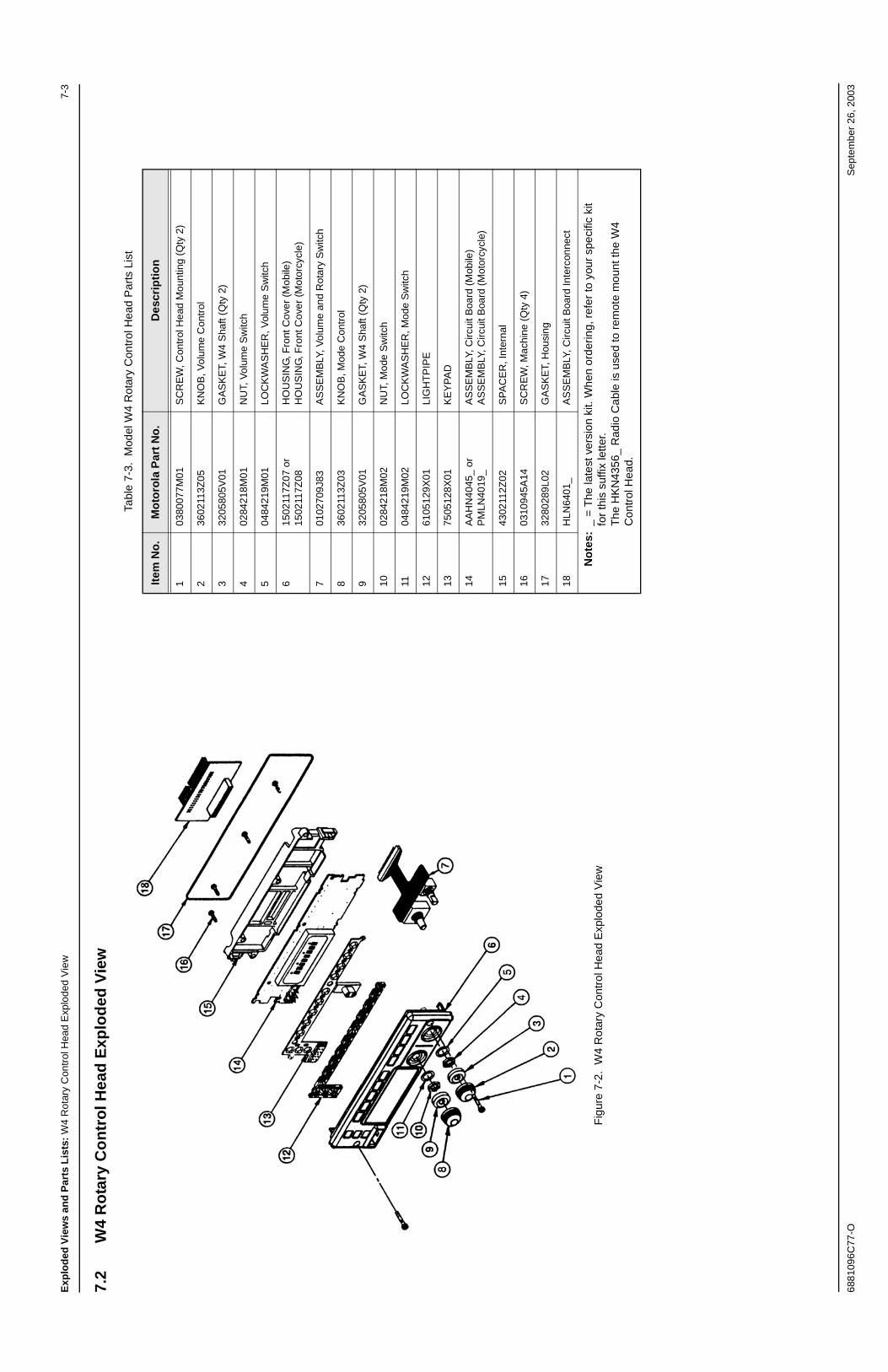
Exp
lod
ed V
iew
s an
d P
arts
Lis
ts:
W4
Rot
ary
Con
trol
Hea
d E
xplo
ded
Vie
w7-
3
6881
096C
77-O
Sep
tem
ber
26, 2
003
7.2
W4
Ro
tary
Co
ntr
ol H
ead
Exp
lod
ed V
iew
Fig
ure
7-2.
W4
Rot
ary
Con
trol
Hea
d E
xplo
ded
Vie
w
Tabl
e 7-
3. M
odel
W4
Rot
ary
Con
trol
Hea
d P
arts
Lis
t
Item
No
.M
oto
rola
Par
t N
o.
Des
crip
tio
n
103
8007
7M01
SC
RE
W, C
ontr
ol H
ead
Mou
ntin
g (Q
ty 2
)
236
0211
3Z05
KN
OB
, Vol
ume
Con
trol
332
0580
5V01
GA
SK
ET,
W4
Sha
ft (Q
ty 2
)
402
8421
8M01
NU
T, V
olum
e S
witc
h
504
8421
9M01
LOC
KW
AS
HE
R, V
olum
e S
witc
h
615
0211
7Z07
or
1502
117Z
08H
OU
SIN
G, F
ront
Cov
er (
Mob
ile)
HO
US
ING
, Fro
nt C
over
(M
otor
cycl
e)
701
0270
9J83
AS
SE
MB
LY, V
olum
e an
d R
otar
y S
witc
h
836
0211
3Z03
KN
OB
, Mod
e C
ontr
ol
932
0580
5V01
GA
SK
ET,
W4
Sha
ft (Q
ty 2
)
1002
8421
8M02
NU
T, M
ode
Sw
itch
1104
8421
9M02
LOC
KW
AS
HE
R, M
ode
Sw
itch
1261
0512
9X01
LIG
HT
PIP
E
1375
0512
8X01
KE
YP
AD
14A
AH
N40
45_
orP
MLN
4019
_A
SS
EM
BLY
, Circ
uit B
oard
(M
obile
)A
SS
EM
BLY
, Circ
uit B
oard
(M
otor
cycl
e)
1543
0211
2Z02
SP
AC
ER
, Int
erna
l
1603
1094
5A14
SC
RE
W, M
achi
ne (
Qty
4)
1732
8028
9L02
GA
SK
ET,
Hou
sing
18H
LN64
01_
AS
SE
MB
LY, C
ircui
t Boa
rd In
terc
onne
ct
No
tes:
_ =
The
late
st v
ersi
on k
it. W
hen
orde
ring,
ref
er to
you
r sp
ecifi
c ki
t fo
r th
is s
uffix
lette
r.T
he H
KN
4356
_ R
adio
Cab
le is
use
d to
rem
ote
mou
nt th
e W
4 C
ontr
ol H
ead.

Sep
tem
ber
26, 2
003
6881
096C
77-O
7-4
Exp
lod
ed V
iew
s an
d P
arts
Lis
ts:
W5
and
W7
Pus
hbut
ton
Con
trol
Hea
d E
xplo
ded
Vie
w
7.3
W5
and
W7
Pu
shb
utt
on
Co
ntr
ol H
ead
Exp
lod
ed V
iew
Fig
ure
7-3.
W5
and
W7
Pus
hbut
ton
Con
trol
Hea
d E
xplo
ded
Vie
w
Tabl
e 7-
4. W
5 an
d W
7 P
ushb
utto
n C
ontr
ol H
ead
Par
ts L
ist
Item
No
.M
oto
rola
Par
t N
o.
Des
crip
tio
n
138
8022
7M04
SW
ITC
H, O
n/O
ff C
ap
238
8000
9P01
SW
ITC
H, M
ode
Roc
ker
338
8000
9P02
SW
ITC
H, V
olum
e R
ocke
r
415
8002
0S17
or
1580
020S
19H
OU
SIN
G, W
5 F
ront
Cov
er (
Mob
ile)
HO
US
ING
, W5
Fro
nt C
over
(M
otor
cycl
e)
538
8009
2J05
PU
SH
BU
TT
ON
, HO
ME
638
8009
2J05
PU
SH
BU
TT
ON
, DIM
703
8007
7M01
SC
RE
W, (
Qty
2)
815
8002
0S16
or
1580
020S
18H
OU
SIN
G, W
7 F
ront
Cov
er (
Mob
ile)
HO
US
ING
, W7
Fro
nt C
over
(M
otor
cycl
e)
961
8001
7S01
LIG
HT
PIP
E
1075
8001
2S03
KE
YP
AD
1143
8001
9S02
SP
AC
ER
, Int
erna
l Fra
me
1203
1094
5A14
SC
RE
W, T
appi
ng (
Qty
7)
1332
8028
9L02
GA
SK
ET,
Hou
sing
14H
LN64
01_
BO
AR
D, I
nter
conn
ect
15H
LN63
96_
orH
LN65
63_
BO
AR
D, C
ontr
ol H
ead
(Mob
ile)
BO
AR
D, C
ontr
ol H
ead
(Mot
orcy
cle)
1601
8004
9S09
or
0180
049S
11 o
r01
8004
9S08
or
0180
049S
10
AS
SE
MB
LY, W
5 F
ront
Cov
er (
Mob
ile)
AS
SE
MB
LY, W
5 F
ront
Cov
er (
Mot
orcy
cle)
AS
SE
MB
LY, W
7 F
ront
Cov
er (
Mob
ile)
AS
SE
MB
LY, W
7 F
ront
Cov
er (
Mot
orcy
cle)
Item
16
incl
udes
item
s 1,
2, 3
, 4 o
r 8,
5, 6
, 9, a
nd 1
0
No
tes:
_ =
The
late
st v
ersi
on k
it. W
hen
orde
ring,
ref
er to
you
r sp
ecifi
c ki
t fo
r th
is s
uffix
lette
r.T
he H
KN
4356
_ R
adio
Cab
le is
use
d to
rem
ote
mou
nt th
e W
5 an
d W
7 C
ontr
ol H
ead.
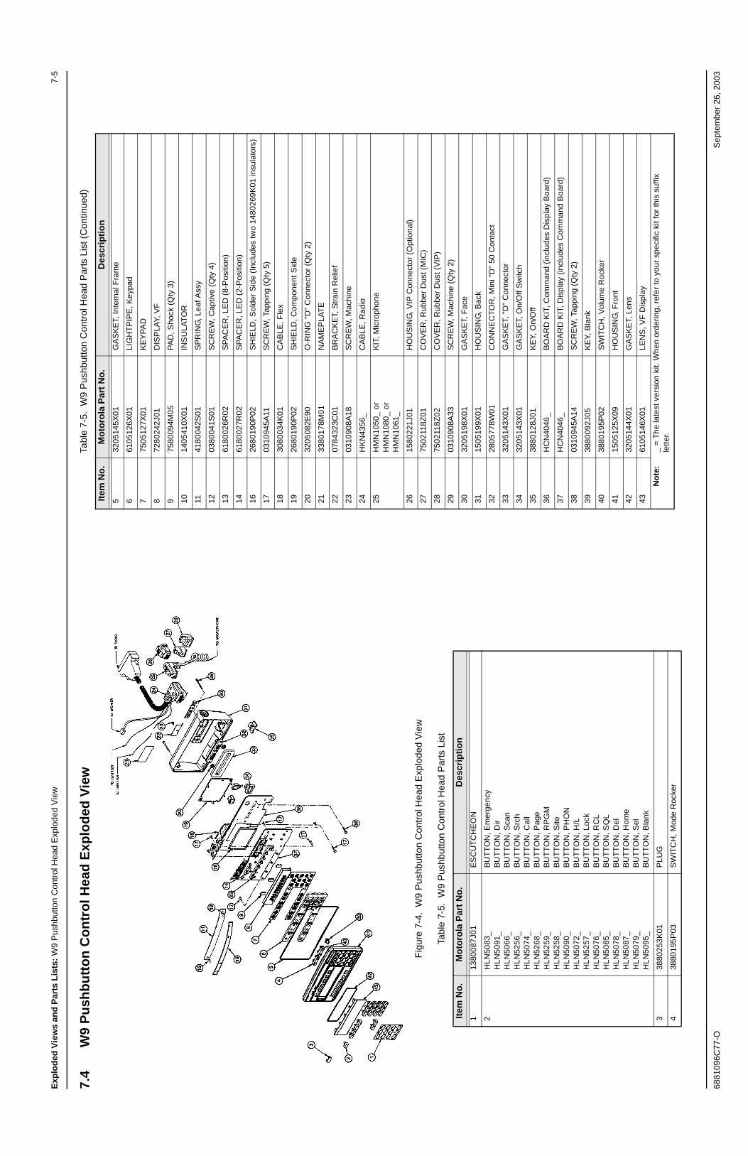
Exp
lod
ed V
iew
s an
d P
arts
Lis
ts:
W9
Pus
hbut
ton
Con
trol
Hea
d E
xplo
ded
Vie
w7-
5
6881
096C
77-O
Sep
tem
ber
26, 2
003
7.4
W9
Pu
shb
utt
on
Co
ntr
ol H
ead
Exp
lod
ed V
iew
Fig
ure
7-4.
W9
Pus
hbut
ton
Con
trol
Hea
d E
xplo
ded
Vie
w
Tabl
e 7-
5. W
9 P
ushb
utto
n C
ontr
ol H
ead
Par
ts L
ist
Item
No
.M
oto
rola
Par
t N
o.
Des
crip
tio
n
113
8008
7J01
ES
CU
TC
HE
ON
2H
LN50
83_
HLN
5091
_H
LN50
66_
HLN
5256
_H
LN50
74_
HLN
5268
_H
LN52
59_
HLN
5258
_H
LN50
90_
HLN
5072
_H
LN52
57_
HLN
5076
_H
LN50
85_
HLN
5078
_H
LN50
87_
HLN
5079
_H
LN50
95_
BU
TT
ON
, Em
erge
ncy
BU
TT
ON
, Dir
BU
TT
ON
, Sca
nB
UT
TO
N, S
rch
BU
TT
ON
, Cal
lB
UT
TO
N, P
age
BU
TT
ON
, RP
GM
BU
TT
ON
, Site
BU
TT
ON
, PH
ON
BU
TT
ON
, H/L
BU
TT
ON
, Loc
kB
UT
TO
N, R
CL
BU
TT
ON
, SQ
LB
UT
TO
N, D
elB
UT
TO
N, H
ome
BU
TT
ON
, Sel
BU
TT
ON
, Bla
nk
338
8025
3K01
PLU
G
438
8019
5P03
SW
ITC
H, M
ode
Roc
ker
532
0514
5X01
GA
SK
ET,
Inte
rnal
Fra
me
661
0512
6X01
LIG
HT
PIP
E, K
eypa
d
775
0512
7X01
KE
YP
AD
872
8024
2J01
DIS
PLA
Y, V
F
975
8009
4M05
PA
D, S
hock
(Q
ty 3
)
1014
0541
0X01
INS
ULA
TO
R
1141
8004
2S01
SP
RIN
G, L
eaf A
ssy
1203
8004
1S01
SC
RE
W, C
aptiv
e (Q
ty 4
)
1361
8002
6R02
SP
AC
ER
, LE
D (
8-P
ositi
on)
1461
8002
7R02
SP
AC
ER
, LE
D (
2-P
ositi
on)
1626
8019
0P02
SH
IELD
, Sol
der
Sid
e (I
nclu
des
two
1480
269K
01 in
sula
tors
)
1703
1094
5A11
SC
RE
W, T
appi
ng (
Qty
5)
1830
8003
4K01
CA
BLE
, Fle
x
1926
8019
0P02
SH
IELD
, Com
pone
nt S
ide
2032
0508
2E90
O-R
ING
"D
" C
onne
ctor
(Q
ty 2
)
2133
8017
8M01
NA
ME
PLA
TE
2207
8432
3C01
BR
AC
KE
T, S
trai
n R
elie
f
2303
1090
8A18
SC
RE
W, M
achi
ne
24H
KN
4356
_C
AB
LE, R
adio
25H
MN
1050
_ or
HM
N10
80_
orH
MN
1061
_
KIT
, Mic
roph
one
2615
8022
1J01
HO
US
ING
, VIP
Con
nect
or (
Opt
iona
l)
2775
0211
8Z01
CO
VE
R, R
ubbe
r D
ust (
MIC
)
2875
0211
8Z02
CO
VE
R, R
ubbe
r D
ust (
VIP
)
2903
1090
8A33
SC
RE
W, M
achi
ne (
Qty
2)
3032
0519
8X01
GA
SK
ET,
Fac
e
3115
0519
9X01
HO
US
ING
, Bac
k
3228
0577
8W01
CO
NN
EC
TO
R, M
ini "
D"
50 C
onta
ct
3332
0514
3X01
GA
SK
ET,
"D
" C
onne
ctor
3432
0514
3X01
GA
SK
ET,
On/
Off
Sw
itch
3538
8012
8J01
KE
Y, O
n/O
ff
36H
CN
4046
_B
OA
RD
KIT
, Com
man
d (in
clud
es D
ispl
ay B
oard
)
37H
CN
4046
_B
OA
RD
KIT
, Dis
play
(in
clud
es C
omm
and
Boa
rd)
3803
1094
5A14
SC
RE
W, T
appi
ng (
Qty
2)
3938
8009
2J05
KE
Y, B
lank
4038
8019
5P02
SW
ITC
H, V
olum
e R
ocke
r
4115
0512
5X09
HO
US
ING
, Fro
nt
4232
0514
4X01
GA
SK
ET,
Len
s
4361
0514
6X01
LEN
S, V
F D
ispl
ay
No
te:
_ =
The
late
st v
ersi
on k
it. W
hen
orde
ring,
ref
er to
you
r sp
ecifi
c ki
t for
this
suf
fix
lette
r.
Tabl
e 7-
5. W
9 P
ushb
utto
n C
ontr
ol H
ead
Par
ts L
ist (
Con
tinue
d)
Item
No
.M
oto
rola
Par
t N
o.
Des
crip
tio
n

7-6
Exp
lod
ed V
iew
s an
d P
arts
Lis
ts:
HM
N10
80A
, HM
N10
61A
, HM
N10
79A
Mic
roph
one
Exp
lode
d V
iew
Sep
tem
ber
26, 2
003
6881
096C
77-O
7.5
HM
N10
80A
, HM
N10
61A
, HM
N10
79A
Mic
rop
ho
ne
Exp
lod
ed V
iew
Fig
ure
7-5.
HM
N10
80A
, HM
N10
61A
, HM
N10
79A
Mic
roph
one
Exp
lode
d V
iew
4
2
1
158
9
3
1013
14
1211
7
MIC
RO
PHO
NE
BOAR
D
MAE
PF-2
7700
-O
56
Tabl
e 7-
6. H
MN
1080
A, H
MN
1061
A, H
MN
1079
A M
icro
phon
e P
arts
Lis
t
Item
No
.M
oto
rola
Par
t N
o.
Des
crip
tio
n
115
8012
7D05
Mic
roph
one
Fro
nt H
ousi
ng
238
8014
4D05
Mic
roph
one
PT
T B
utto
n
330
8022
3J05
or
3080
210P
01 o
r30
8022
3J01
HM
N10
80A
Coi
led
6 C
ond
HM
N10
79A
Coi
led
6 C
ond
HM
N10
61A
Coi
led
6 C
ond
405
8022
1K01
PT
T S
witc
h G
rom
met
503
1094
3M09
Tapp
ing
Scr
ew (
3 x
0.5
x 6)
630
8020
6L01
PC
B to
Mic
Wei
ght W
ire
732
8005
8H03
Hou
sing
Gas
ket
801
8075
0T91
Mic
roph
one
Rea
r H
ousi
ng
903
8007
6E04
Hi-l
o M
etric
Scr
ew
1003
1200
2C01
Scr
ew, S
elf-
drill
ing,
6-2
0 x
1/2”
1135
8008
9D01
Mic
roph
one
Fel
t Baf
fle
1205
8014
8D01
Mic
roph
one
Gro
mm
et
1301
8074
3T91
Han
gup
Clip
1401
8075
0T52
Gro
und
Wire
1503
0013
8015
Scr
ew, S
elf-
drill
ing,
8-1
8 x
1/2”

Exp
lod
ed V
iew
s an
d P
arts
Lis
ts:
Sm
all P
ushb
utto
n P
arts
7-7
6881
096C
77-O
Sep
tem
ber
26, 2
003
7.6
Sm
all P
ush
bu
tto
n P
arts
7.7
Lar
ge
Pu
shb
utt
on
Par
ts
Tabl
e 7-
7. S
mal
l Pus
hbut
ton
Par
ts L
ist
Par
t N
um
ber
Gra
ph
ic
Leg
end
Par
t N
um
ber
Gra
ph
ic
Leg
end
3805
671X
021
3805
671X
219w
xy
3805
671X
032
3805
671X
22*
Rcl
3805
671X
043
3805
671X
23#D
el
3805
671X
054
3805
671X
241S
te
3805
671X
065
3805
671X
252P
ge
3805
671X
076
3805
671X
263L
ck
3805
671X
087
3805
671X
274S
ts
3805
671X
098
3805
671X
285R
pg
3805
671X
109
3805
671X
296M
sg
3805
671X
110
3805
671X
307H
/L
3805
671X
12*
3805
671X
318M
on
3805
671X
13#
3805
671X
329D
ir
3805
671X
142a
bc38
0567
1X33
Mon
3805
671X
153d
ef38
0567
1X34
H/L
3805
671X
164g
hi38
0567
1X35
DIR
3805
671X
175j
kl38
0567
1X36
Urg
3805
671X
186m
no38
0567
1X37
RT
T
3805
671X
197p
rs38
0567
1X38
Hom
e
3805
671X
208t
uv38
0567
1X39
Dim
Tabl
e 7-
8. L
arge
Pus
hbut
ton
Par
ts L
ist
Par
t N
um
ber
Gra
ph
ic
Leg
end
Par
t N
um
ber
Gra
ph
ic
Leg
end
3805
672X
01-
-38
0567
2X10
H/L
3805
672X
02M
PL
3805
672X
11S
ts
3805
672X
03S
can
3805
672X
12C
all
3805
672X
04D
VP
3805
672X
13M
sg
3805
672X
05P
A38
0567
2X14
Rcl
3805
672X
06S
irn38
0567
2X15
Mod
e
3805
672X
07W
ail
3805
672X
16E
xRd
3805
672X
08H
i/Lo
3805
672X
17D
el
3805
672X
09M
an38
0567
2X18
Sel
3805
672X
19M
on38
0567
2X52
Em
er
3805
672X
20D
TM
F38
0567
2X53
Std
y
3805
672X
21Ye
lp38
0567
2X54
EC
C
3805
672X
22M
VS
3805
672X
55R
ptr
3805
672X
23P
lay
3805
672X
56S
tate
3805
672X
24R
ply
3805
672X
57R
eg
3805
672X
25R
crd
3805
672X
58A
irHn
3805
672X
26E
mer
3805
672X
59T
B S
cn
3805
672X
27E
xt38
0567
2X60
SC
C
3805
672X
28F
/R38
0567
2X61
Src
h
3805
672X
29A
lt38
0567
2X62
Lock
3805
672X
30Te
l38
0567
2X63
Pag
e
3805
672X
31S
ql38
0567
2X64
Rea
r
3805
672X
32D
ES
3805
672X
65X
fer
3805
672X
33T
xt38
0567
2X66
ST
3805
672X
34In
dv38
0567
2X67
VH
F
3805
672X
35P
vt38
0567
2X68
UH
F
3805
672X
36S
ite38
0567
2X69
Aux
3805
672X
37A
A38
0567
2X70
QC
II
3805
672X
38S
ub38
0567
2X71
Mut
e
3805
672X
39H
ome
3805
672X
72P
ri
3805
672X
40M
enu
3805
672X
73B
lu
3805
672X
41R
pgm
3805
672X
74D
iv
3805
672X
42S
tep
3805
672X
75R
TT
3805
672X
4338
0567
2X76
Sen
d
3805
672X
44P
hon
3805
672X
77F
ront
3805
672X
45D
ir38
0567
2X78
Bid
3805
672X
46Te
xt38
0567
2X79
ZO
NE
3805
672X
47R
vw38
0567
2X80
TR
BL
3805
672X
48S
ec38
0567
2X81
OV
HD
3805
672X
49Ø
3805
672X
82U
NG
D
3805
672X
50L/
S38
0567
2X83
RS
SI
3805
672X
51S
/S38
0567
2X84
VR
S
3805
672X
85A
/B38
0566
9X12
ETr
p
3805
672X
86C
han
3805
669X
13Lv
Te
3805
672X
87P
RT
T38
0566
9X14
ArT
e
3805
672X
88R
tRn
3805
669X
15Lv
Gg
3805
672X
89E
mp#
3805
669X
16A
rGg
3805
672X
90P
ass
3805
669X
17P
/in
3805
672X
91C
ir38
0566
9X18
P/o
ut
3805
672X
92U
RG
3805
669X
19S
erv
3805
672X
93A
3805
669X
200/
S
3805
672X
94B
3805
669X
21R
ev
3805
672X
95C
3805
669X
22S
tby
3805
672X
96D
3805
669X
23S
ts 1
3805
672X
97E
3805
669X
24S
ts 2
3805
672X
98F
3805
669X
25S
ts 3
3805
672X
99G
3805
669X
26S
ts 4
3805
669X
01K
3805
669X
27S
ts 5
3805
669X
02L
3805
669X
28S
ts 6
3805
669X
03T
/Z38
0566
9X29
Sts
7
3805
669X
0430
3805
669X
30S
ts 8
Tabl
e 7-
8. L
arge
Pus
hbut
ton
Par
ts L
ist (
Con
tinue
d)
Par
t N
um
ber
Gra
ph
ic
Leg
end
Par
t N
um
ber
Gra
ph
ic
Leg
end
3805
669X
05E
ntr
3805
669X
31D
rvr
3805
669X
06M
/WT
3805
669X
32B
dg#
3805
669X
07M
Ack
3805
669X
33Ln
BI
3805
669X
08Ti
me
3805
669X
34R
tBl
3805
669X
09S
Run
3805
669X
35Ln
Rn
3805
669X
10E
Run
3805
669X
36s
3805
669X
11S
Trp
3805
669X
37t
3800
028M
01“E
mer
Hou
sing
”38
0002
9M01
“Em
er P
lung
er”
Tabl
e 7-
8. L
arge
Pus
hbut
ton
Par
ts L
ist (
Con
tinue
d)
Par
t N
um
ber
Gra
ph
ic
Leg
end
Par
t N
um
ber
Gra
ph
ic
Leg
end
7-8
Exp
lod
ed V
iew
s an
d P
arts
Lis
ts:
Larg
e P
ushb
utto
n P
arts
Sep
tem
ber
26, 2
003
6881
096C
77-O
No
tes

Sch
emat
ics,
Ove
rlay
s, a
nd
Par
ts L
ists
: Li
st o
f Sch
emat
ics,
Com
pone
nt L
ocat
ion
Dia
gram
s, a
nd P
arts
Lis
ts8-
1
6881
096C
77-O
Sep
tem
ber
26, 2
003
Ch
apte
r 8
Sch
emat
ics,
Ove
rlay
s, a
nd
Par
ts L
ists
8.1
Lis
t o
f S
chem
atic
s, C
om
po
nen
t L
oca
tio
n D
iag
ram
s, a
nd
Par
ts
Lis
tsT
he fo
llow
ing
tabl
e lis
ts th
e sc
hem
atic
s,
com
pone
nt lo
catio
n di
agra
ms,
and
par
ts li
sts
cont
aine
d in
this
cha
pter
.
Tabl
e 8-
1. L
ist o
f Sch
emat
ics,
Com
pone
nt L
ocat
ion
Dia
gram
s, a
nd P
arts
Lis
ts
Fig
ure
Tit
leP
age
HM
N40
44E
W3
Con
trol
Hea
d S
chem
atic
8-2
HM
N40
44E
W3
Con
trol
Hea
d C
ompo
nent
Loc
atio
n D
iagr
am8-
3
HM
N40
44E
W3
Con
trol
Hea
d C
ompo
nent
Loc
atio
n D
iagr
am8-
4
HM
N40
44E
Par
ts L
ist
8-5
HK
N60
96B
Rem
ote
“Y”
Cab
le W
iring
Dia
gram
8-6
AA
HN
4045
F/G
(S
tand
ard)
, HLN
4071
A/B
(R
ear)
, P
MLN
4019
C/D
(M
otor
cycl
e) W
4 C
ontr
ol H
ead
Sch
emat
ic (
She
et 1
of 2
)
8-7
AA
HN
4045
F/G
(S
tand
ard)
, HLN
4071
A/B
(R
ear)
, P
MLN
4019
C/D
(M
otor
cycl
e) W
4 C
ontr
ol H
ead
Sch
emat
ic (
She
et 2
of 2
)
8-8
AA
HN
4045
(Sta
ndar
d), H
LN40
71 (R
ear)
, PM
LN40
19
(Mot
orcy
cle)
W4
Con
trol
Hea
d C
ompo
nent
Loc
atio
n D
iagr
am
8-9
AA
HN
4045
G S
tand
ard
Par
ts L
ist
8-10
HC
N40
71B
Rea
r P
arts
Lis
t8-
12
PM
LN40
19D
Mot
orcy
cle
Par
ts L
ist
8-14
HLN
6396
F/G
/H (
Sta
ndar
d), H
LN68
14A
/B/C
(R
ear)
, H
LN65
63B
/C/D
(M
otor
cycl
e) W
5/W
7 C
ontr
ol H
ead
Sch
emat
ic (
She
et 1
of 2
)
8-16
HLN
6396
F/G
/H (
Sta
ndar
d),H
LN68
14A
/B/C
(R
ear)
, H
LN65
63B
/C/D
(M
otor
cycl
e) W
5/W
7 C
ontr
ol H
ead
Sch
emat
ic (
She
et 2
of 2
)
8-17
HLN
6396
F/G
(S
tand
ard)
, HLN
6814
A/B
(R
ear)
, H
LN65
63B
/C (
Mot
orcy
cle)
W5/
W7
Con
trol
Hea
d C
ompo
nent
Loc
atio
n D
iagr
am (
Vie
wed
from
Sid
e 1)
8-18
HLN
6396
F/G
(S
tand
ard)
, HLN
6814
A/B
(R
ear)
, H
LN65
63B
/C (
Mot
orcy
cle)
W5/
W7
Con
trol
Hea
d C
ompo
nent
Loc
atio
n D
iagr
am (
Vie
wed
from
Sid
e 2)
8-18
HLN
6396
H_H
LN68
14C
_HLN
6563
C W
5/W
7 C
ontr
ol
Hea
d C
ompo
nent
Loc
atio
n D
iagr
am (
Vie
wed
from
S
ide
1)
8-19
HLN
6396
H_H
LN68
14C
_HLN
6563
C W
5/W
7 C
ontr
ol
Hea
d C
ompo
nent
Loc
atio
n D
iagr
am (
Vie
wed
from
S
ide
2)
8-19
HLN
6396
H S
tand
ard
Par
ts L
ist
8-20
HLN
6814
C R
ear
Par
ts L
ist
8-22
HLN
6563
D M
otor
cycl
e P
arts
Lis
t8-
24
HC
N10
78J
(Sta
ndar
d), H
CN
1121
D (
Rea
r) W
9 C
ontr
ol H
ead
Sch
emat
ic (
Sid
e 1
of 2
)8-
26
HC
N10
78J
(Sta
ndar
d), H
CN
1121
D (
Rea
r) W
9 C
ontr
ol H
ead
Sch
emat
ic (
Sid
e 2
of 2
)8-
27
HC
N10
78J
(Sta
ndar
d), H
CN
1121
D (
Rea
r) W
9 C
ontr
ol H
ead
Com
pone
nt L
ocat
ion
Dia
gram
(Vie
wed
fr
om S
ide
1)
8-28
HC
N10
78J
(Sta
ndar
d), H
CN
1121
D (
Rea
r) W
9 C
ontr
ol H
ead
Com
pone
nt L
ocat
ion
Dia
gram
(Vie
wed
fr
om S
ide
2)
8-29
HC
N10
78J
(Sta
ndar
d), H
CN
1121
D (
Rea
r) P
arts
Lis
t8-
30
W4,
W5,
and
W7
Con
trol
Hea
d Lo
w-/
Mid
-Pow
er
Inte
rcon
nect
ion
Dia
gram
8-33
W4,
W5,
and
W7
Hig
h P
ower
Inte
rcon
nect
ion
Dia
gram
8-34
W5
and
W7
Con
trol
Hea
d In
terf
ace
Boa
rd S
chem
atic
8-35
HLN
6432
D W
5/W
7 C
ontr
ol H
ead
Inte
rfac
e B
oard
C
ompo
nent
Loc
atio
n D
iagr
am8-
36
HLN
6401
A C
ontr
ol H
ead
Inte
rcon
nect
Boa
rd, (
Das
h-M
ount
)8-
37
HLN
6486
D/E
Hig
h P
ower
Sta
ndar
d In
terc
onne
ct
Boa
rd8-
38
HLN
6486
D/E
Hig
h-P
ower
Inte
rcon
nect
Boa
rd
(Vie
wed
from
Sid
e 1)
8-39
HLN
6486
D/E
Hig
h-P
ower
Inte
rcon
nect
Boa
rd
(Vie
wed
from
Sid
e 2)
8-39
HLN
6486
E S
tand
ard
Inte
rcon
nect
Par
ts L
ist
8-40
HLN
6574
E W
3 C
ontr
ol H
ead
Hig
h-P
ower
In
terc
onne
ct B
oard
Sch
emat
ic D
esig
n8-
41
Tabl
e 8-
1. L
ist o
f Sch
emat
ics,
Com
pone
nt L
ocat
ion
Dia
gram
s, a
nd P
arts
Lis
ts (
Con
tinue
d)
Fig
ure
Tit
leP
age
HLN
6574
E W
3 H
igh
Pow
er In
terc
onne
ct B
oard
C
ompo
nent
Loc
atio
n D
iagr
ams
8-42
HLN
6574
E W
3 H
igh-
Pow
er In
terc
onne
ct P
arts
Lis
t8-
43
HLN
6459
D, H
LN63
44E
, and
HLN
6365
E L
ow-P
ower
In
terc
onne
ct B
oard
Sch
emat
ic8-
45
HLN
6459
D, H
LN63
44E
, and
HLN
6365
Low
-Pow
er
Inte
rcon
nect
Com
pone
nt L
ocat
ion
Dia
gram
8-46
HLN
6459
D W
3 Lo
w-P
ower
Inte
rcon
nect
Par
ts L
ist
8-47
HLN
6365
E M
otor
cycl
e In
terc
onne
ct P
arts
Lis
t8-
49
HLN
6344
E S
tand
ard
Inte
rcon
nect
Par
ts L
ist
8-50
HM
N10
80A
, HM
N10
61A
, HM
N10
79A
Mic
roph
one
Boa
rd O
verla
y8-
51
HM
N10
80A
, HM
N10
61A
, HM
N10
79A
Mic
roph
one
Sch
emat
ic8-
51
HM
N10
80A
, HM
N10
61A
, HM
N10
79A
Mic
roph
one
Par
ts L
ist
8-51
Tabl
e 8-
1. L
ist o
f Sch
emat
ics,
Com
pone
nt L
ocat
ion
Dia
gram
s, a
nd P
arts
Lis
ts (
Con
tinue
d)
Fig
ure
Tit
leP
age

8-2
Sch
emat
ics,
Ove
rlay
s, a
nd
Par
ts L
ists
: Li
st o
f Sch
emat
ics,
Com
pone
nt L
ocat
ion
Dia
gram
s, a
nd P
arts
Lis
ts
Sep
tem
ber
26, 2
003
6881
096C
77-O
Fig
ure
8-1.
HM
N40
44E
W3
Con
trol
Hea
d S
chem
atic
(For
ref
eren
ce o
nly
- bo
ard
is n
ot fi
eld-
repa
irabl
e)
63B
8108
4C78
-O

Sch
emat
ics,
Ove
rlay
s, a
nd
Par
ts L
ists
: Li
st o
f Sch
emat
ics,
Com
pone
nt L
ocat
ion
Dia
gram
s, a
nd P
arts
Lis
ts8-
3
6881
096C
77-O
Sep
tem
ber
26, 2
003
Fig
ure
8-2.
HM
N40
44E
W3
Con
trol
Hea
d C
ompo
nent
Loc
atio
n D
iagr
am
MA
EP
F-2
5560
-O
(Vie
wed
from
Sid
e 1)
(For
ref
eren
ce o
nly
- bo
ard
is n
ot fi
eld-
repa
irabl
e)

8-4
Sch
emat
ics,
Ove
rlay
s, a
nd
Par
ts L
ists
: Li
st o
f Sch
emat
ics,
Com
pone
nt L
ocat
ion
Dia
gram
s, a
nd P
arts
Lis
ts
Sep
tem
ber
26, 2
003
6881
096C
77-O
Fig
ure
8-3.
HM
N40
44E
W3
Con
trol
Hea
d C
ompo
nent
Loc
atio
n D
iagr
am
MA
EP
F-2
5561
-O
(Vie
wed
from
Sid
e 2)
(For
ref
eren
ce o
nly
- bo
ard
is n
ot fi
eld-
repa
irabl
e)

Sch
emat
ics,
Ove
rlay
s, a
nd
Par
ts L
ists
: Li
st o
f Sch
emat
ics,
Com
pone
nt L
ocat
ion
Dia
gram
s, a
nd P
arts
Lis
ts8-
5
6881
096C
77-O
Sep
tem
ber
26, 2
003
HM
N40
44E
Par
ts L
ist
(Fo
r re
fere
nce
on
ly -
bo
ard
is n
ot
fiel
d-r
epai
rab
le)
ITE
MM
OTO
RO
LA
PA
RT
N
UM
BE
RD
ES
CR
IPT
ION
C1
2380
090M
2410
µF ±
20%
; 50V
C2
2113
743A
190.
1µF
C3
2113
740F
5110
0pF
C4
2113
743A
190.
1µF
C5
2311
049A
071µ
F ±
1%
; 16V
C6
2113
743A
190.
1µF
C8-
C10
2113
743A
190.
1µF
C11
2113
740F
5110
0pF
C12
2113
741F
2510
00pF
C13
2113
740F
5110
0pF
C15
2113
743A
190.
1µF
C17
-C18
2113
740F
3727
pF
C21
2311
049A
071µ
F ±
1%
; 16V
C22
2311
049A
5710
µF ±
1%;
C23
2113
743A
190.
1µF
C24
2113
743A
190.
1µF
C27
2113
741A
61.0
47µF
C28
-C29
2113
741F
2510
00pF
C30
2113
741A
61.0
47µF
C32
2113
741F
2510
00pF
C34
-C35
2113
741F
49.0
10µF
C36
2113
741F
2510
00pF
C37
2311
049A
5710
µF ±
1%; 1
6V
C38
2113
741F
2510
00pF
C39
2113
743A
190.
1µF
C40
2113
741F
2510
00pF
C41
2113
740F
5922
0pF
C80
2113
741F
2510
00pF
D1
4813
830A
15Z
ener
; 5.6
V
D3-
D16
4805
729G
75LE
D G
reen
D17
-D18
4805
729G
85LE
D G
reen
D19
4805
729G
82LE
D Y
ello
w
D21
4805
729G
83LE
D G
reen
D22
4805
729G
81LE
D R
ed
D24
4880
140L
2520
V
D25
-D27
4813
833C
05D
ual;
70V
D28
-D29
4805
729G
85LE
D G
reen
D30
4813
833C
05D
ual;
70V
D32
4813
833C
05D
ual;
70V
D35
4813
833C
05D
ual;
70V
D37
-D39
4813
833C
05D
ual;
70V
D80
-D81
4813
833C
05 D
ual;
70V
J109
8487
5T03
Jack
L124
8014
0E01
1.2µ
H
P1
2809
926G
01H
eade
r
Q1
4805
128M
12S
OT
Q2
4880
214G
02M
MB
T 3
904
Q3
4805
128M
12S
OT
Q4
4805
780V
01
Q5-
Q8
4880
214G
02M
MB
T 3
904
Q9
4805
128M
12S
OT
Q10
4880
214G
02M
MB
T 3
904
R1
0662
057A
3322
0
R2
0662
057A
1851
R3
0662
057A
531.
5k
R4
0662
057A
654.
7k
R5
0662
057A
613.
3k
R7
0662
057A
654.
7k
R8
0662
057A
7512
k
R9
0662
057A
1851
R10
0662
057A
654.
7k
R11
-R12
0662
057A
9710
0k
R13
0662
057A
1851
R14
0662
057A
9710
0k
R15
0662
057A
654.
7k
ITE
MM
OT
OR
OL
A
PAR
T
NU
MB
ER
DE
SC
RIP
TIO
N
R16
-R20
0662
057A
8122
k
R22
0662
057A
9710
0k
R26
-R27
0662
057B
221M
R28
-R29
0662
057A
9710
0k
R30
0662
057A
8122
k
R31
0662
057A
9710
0k
R32
0662
057A
8122
k
R33
0662
057A
531.
5k
R34
0662
057A
0110
R36
0662
057A
9710
0k
R41
0662
057A
9710
0k
R42
-R43
0662
057A
3322
0
R44
0662
057A
654.
7k
R46
0662
057B
221M
R50
0662
057B
1033
0k
R51
0662
057A
654.
7k
R52
0662
057A
572.
2k
R54
0662
057B
0215
0k
R55
0662
057A
7512
k
R56
0662
057A
9710
0k
R63
0662
057A
0110
R64
0662
057B
470
R65
0662
057A
613.
3k
R68
0662
057B
0215
0k
R70
0662
057A
1539
R71
0662
057A
572.
2k
R73
-R74
0662
057A
8122
k
R75
0662
057A
531.
5k
R80
-R81
0662
057A
9710
0k
R82
0662
057A
8122
k
R83
0662
057A
9710
0k
R10
0-R
105
0662
057A
3322
0
R10
6-R
107
0662
057A
1539
ITE
MM
OT
OR
OL
A
PA
RT
N
UM
BE
RD
ES
CR
IPT
ION
R10
806
6205
7A33
220
R10
906
6205
7A69
6.8k
S1-
S7
4005
840X
01
U1
5105
469E
65V
olta
ge R
egul
ator
U2
5105
663U
34IC
Com
para
tor
U3
5113
802A
07IC
Com
para
tor
µP
U4
5102
074D
01LD
C
U5-
U7
5102
074D
01D
river
U8
5113
805A
758-
Bit
Shi
ft R
egis
ter
U9
5105
625U
63IC
Vol
tage
Det
ecto
r
U10
5113
805A
74S
hift
Reg
iste
r
U13
0604
267J
01In
-line
Res
isto
r P
acka
ge
U14
5102
073D
01A
nalo
g/D
igita
l Con
vert
er
Y1
4880
065M
01R
eson
ator
; 4.0
MH
z
ITE
MM
OTO
RO
LA
P
AR
T
NU
MB
ER
DE
SC
RIP
TIO
N

8-6
Sch
emat
ics,
Ove
rlay
s, a
nd
Par
ts L
ists
: Li
st o
f Sch
emat
ics,
Com
pone
nt L
ocat
ion
Dia
gram
s, a
nd P
arts
Lis
ts
Sep
tem
ber
26, 2
003
6881
096C
77-O
Fig
ure
8-4.
HK
N60
96B
Rem
ote
“Y”
Cab
le W
iring
Dia
gram
WH
T/B
LUE
5W
HT
/BLU
E5
J1
J2
P1
YE
LLO
W/B
LK14
YE
LLO
W/R
ED
23D
RA
IN18
WH
T/B
LK17
NC
15N
C19
NC
20G
RA
Y4
OR
AN
GE
3Y
ELL
OW
/GR
N
OR
AN
GE
/BLU
E
OR
AN
GE
/BLU
E
12N
C10
DR
AIN
11B
LAC
K22
NC
21G
RE
EN
13B
RO
WN
25R
ED
24N
C6
NC
PIN
1
PIN
1
PIN
8P
IN 1
5
PIN
9
PIN
1
PIN
13
PIN
13
PIN
14
PIN
14
PIN
25
PIN
25
9N
C1
YE
LLO
W/B
LK14
YE
LLO
W/R
ED
23D
RA
IN18
NC
19N
C1
NC
6N
C10
GR
AY
4N
C2
YE
LLO
W/G
RN
12N
C21
DR
AIN
11B
LAC
K22
OR
AN
GE
5B
LAC
K4
YE
LLO
W12
GR
EE
N2
BR
OW
N6
RE
D7
NC
14N
C11
GR
AY
8N
C10
NC
9N
C1
WH
T/B
LK
CO
NN
EC
TO
RM
ET
AL
SH
RO
UD
SO
LDE
R W
IRE
SE
CU
RE
LYIN
PO
SIT
ION
3
BR
OW
N25
RE
D24
NC
2N
C7
NC
8Y
ELL
OW
8G
RE
EN
WH
T/B
LK
OR
AN
GE
YE
LLO
W
MA
EP
F-2
5562
-O

Sch
emat
ics,
Ove
rlay
s, a
nd
Par
ts L
ists
: Li
st o
f Sch
emat
ics,
Com
pone
nt L
ocat
ion
Dia
gram
s, a
nd P
arts
Lis
ts8-
7
6881
096C
77-O
Sep
tem
ber
26, 2
003
Fig
ure
8-5.
AA
HN
4045
F/G
(S
tand
ard)
, HLN
4071
A/B
(R
ear)
, PM
LN40
19C
/D (
Mot
orcy
cle)
W4
Con
trol
Hea
d S
chem
atic
(S
heet
1 o
f 2)
BUSY
_IN
*
BUSY
_OU
T*
IGN
*
VIP_
IN_3
*
A+
0.1u
FC
48
CR
55
J2
JU20
STR
OBE
J1
HU
B_IN
V
PTT
VIP_
IN_2
*
RES
ET*
TX_D
ATA
RX_
DAT
A
470p
F
+5V
VIP_
IN_1
*
R98
*
C41
R25
47K
100K
R34
47K
R74
100K
+5V
4.7K
R17
7
JU18
*
VIP_
OU
T_2
R77Q
75
470
R76
Q74
470
R80
100K
CR
73
CR
72
1uF
R79
CR
71
C6
470
CR
76
SP-2
_VF-
SEN
SE-2
SP-1
_VF-
SEN
SE-1
+5V
4.7K
R17
6
VIP_
OU
T_3
JU8*
SWB+
VIP_
OU
T_1
JU4*
SWB+
33K
R73
0.1u
FQ
72
SWB+
C82
470p
FC
175
JU14
*
470
SWB+
R71
Q71 SW
B+
470p
F
JU12
*
+5V
C17
6
+5V
R1*
+5V
4.7K
R17
5
10K
NC
JU9*
JU6*
R17
4
JU13
*
SWB+
4.7K
VR3
Q73
15V
VR4
15V
R31
VR20
15V
47K
15V
VR22
15V
VR21
JU5
18
JU3
SWB+
SWB+
470p
FC
174
268 1419
1MEG
7
R10
+5V
10K
+5VR99
JU15
*
C7
.01u
F
.01u
FC
1
10K
R81
1617
10K
R87
R84
1510
K
15V
15V
VR9
VR8
VR10
15V
10 1598 26 74
15V
3
VR2
VR1
15V
15V
VR7
23
MIC
HI
GN
D
GN
D
A+IGN
SWB+
SWB+
BUS+
BUS-
BUSY
RES
ET
VIP
IN 3
VIP
IN 2
VIP
IN 1
VIPO
UT
3
KEY
SLO
T
VIPO
UT2
VIPO
UT1
P103
SER
IAL
I/O
P104
R7
SW1
45
2. P
ART
USA
GE
MAY
VAR
Y W
ITH
APP
LIC
ATIO
N.
REF
ER T
O P
ARTS
LIS
T FO
R U
SAG
E IN
FOR
MAT
ION
.1.
ALL
RES
ISTA
NC
E IS
IN O
HM
S. A
LL C
APAC
ITAN
CE
IN P
ICO
-FAR
ADS
UN
LESS
NO
TED
OTH
ERW
ISE.
NO
TES:
S.N
ET-K
IDS.
NET
-KEY
S.N
ET-W
E
MIC
LO
MIC
HI
HU
B
PTT
SP-2
/VF-
SEN
SE-2
SP-1
/VF-
SEN
SE-1
HU
B
PTT
S.N
ET-K
ID
S.N
ET-K
EY
S.N
ET-W
E
MIC
LO
17BU
S_PO
SBU
S_N
EG16
BUSY
_OU
T*13
BUSY
_IN
*11
BUSY
10
A+/IGN39
U4
SP1
SP2
(NO
TE 2
)R
OTA
RY
14
IGN
*29
IGN
28
HU
B_PO
L32
HU
B_IN
V30
34GND2
5GND1GND
1
41
15332627408
38
+5V_REG36
+5V
42 231812
25
TX_D
ATA
19
RX_
DAT
A20
RES
_HU
B31
RES
ET_F
ILTR
7
RES
ET*
49
RES
ET
PTT*
37
PTT
WD
T_TI
CKL
E2
WD
T_IN
_T_C
AP44
VIP_
IN_3
*36
VIP_
IN_2
*21
VIP_
IN_1
*24
35VI
P_IN
_3VI
P_IN
_222
VIP_
IN_1
SC74
487F
WD
T_T_
CAP
43
U45
OU
T3
IN1
GND
2
MC
78M
05
1 224 282021 927 313
C45
10uF
470p
FC
57.0
1uF
C58
5 6
+5V
JU1*
11
JU2*
VR5
15V
12 4
A+
22
SWB+
25 10
10K
R9*
VR6
15V
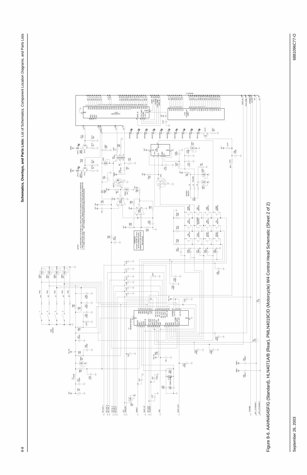
8-8
Sch
emat
ics,
Ove
rlay
s, a
nd
Par
ts L
ists
: Li
st o
f Sch
emat
ics,
Com
pone
nt L
ocat
ion
Dia
gram
s, a
nd P
arts
Lis
ts
Sep
tem
ber
26, 2
003
6881
096C
77-O
Fig
ure
8-6.
AA
HN
4045
F/G
(S
tand
ard)
, HLN
4071
A/B
(R
ear)
, PM
LN40
19C
/D (
Mot
orcy
cle)
W4
Con
trol
Hea
d S
chem
atic
(S
heet
2 o
f 2)
C23
C50
10uF
DAT
A_IN
LTC
H_E
NBL
SP-2
_VF-
SEN
SE-2
STR
OBE
STR
OBE
G8
P0
BUS3(32:1)
SP-1
_VF-
SEN
SE-1
IGN
*
VIP_
OU
T_2
VIP_
OU
T_3
VIP_
OU
T_1
PTT
R13
1
10K
WIT
H P
OW
ER A
PPLI
ED.
3.2. P
ART
USA
GE
MAY
VAR
Y W
ITH
APP
LIC
ATIO
N.
REF
ER T
O P
ARTS
LIS
T FO
R U
SAG
E IN
FOR
MAT
ION
.1.
ALL
RES
ISTA
NC
E IS
IN O
HM
S. A
LL C
APAC
ITAN
CE
IN P
ICO
-FAR
ADS
UN
LESS
NO
TED
OTH
ERW
ISE.
BUSY
XMIT
D
GS
WAR
NIN
G!
(RED
)(Y
ELLO
W)
U10
2
2
3
VOLU
ME
R7
SW1
RO
TAR
YSW
ITC
H
RO
TAR
Y
P001
P001
P001
P001
P001
1 2 3 5
SW2
1
DAM
AGE
TO T
HE
CIR
CU
IT
U1
PIN
S 3,
18,2
3,40
AR
EN
OT
CO
NN
ECTE
D W
ITHM
C68
HC
05C
8A
NO
TES:
MAY
OC
CU
R.
MIC
RO
PRO
CES
SOR
DO
NO
T PR
OBE
U3
PIN
5
C40
470p
F
3
470p
FC
39
10134 26 27
1000
uFC
53
C18
*
CR
137
32
1116
10K
R52
22K
ZUSW
ITC
H
+5V
NC
1
R20
0
33K
18
1 2 3
4 5 6
+5V
R56
Q9
342
24LT
CH
_EN
BL VCC144VDISP1
77J0
3T6
0
Q30
54Q
31Q
323
Q4
39Q
53837
Q6
Q7
36Q
835
Q23
1312Q
24Q
2511
Q26
10Q
2798
Q28
Q29
7
Q3
4025Q
16
20Q
17Q
1819
Q19
17 41Q
2
16Q
20Q
2115
Q22
14
NC
429
42Q
1
Q10
33Q
1132
Q12
3130Q
13Q
1427
Q15
26
STR
OBE
21
CLK
23
DAT
A_IN
43
GND22
6N
C1
NC
218
NC
328
10V
U101UCQ5818EPF
470p
F
VR24
470p
FC
30
C14
1
470p
FC
17
CR
136
3
36V
VR50
JU17
*JU
16
CR
131
CR
132
CR
133
CR
134
C19
*
22 192032
10K
15 16
R14
0
C16
*
8
C15
*
VR31
10V
C44
*
J7J8 J9J6
J5
VR32
10V
J4
VR33
10V
R12
3
R8
+5V
10K
+5V
100
30 29
100
R6
0.1u
F
28
C81
C14
047
0pF
Q76
VSS22
1
J3
CLO
CK
36 37W
DT_
TKL
IGN
*39
RES
ET*
1
BUSY
_IN
41
STR
OBE
38
VDD444
VIP_
OU
T_2
27 26VI
P_O
UT_
1BU
SY_I
N25 24
RX_
DAT
A32
TX_D
ATA
33
DAT
A_IN
34
DAT
A_IN
35
PB4
17 19BK
LTH
UB
20PT
T21
VIP_
IN_3
31VI
P_IN
_230
VIP_
IN_1
29VI
P_O
UT_
328
PA4
8 7LT
CH
_EN
BLH
V_C
NTR
L6
BUSY
_OU
T5
PB0
13PB
114
PB2
15PB
316 23
+5V_
FIL
40
OSC
143
OSC
242
PA0
12
PA1
11
PA2
10
PA3
9
MC
68H
C70
5C8A
U1
2IR
Q*
3+5
V_FI
L18
CR
51
U3A
LM29
03
2 31
8 4
470p
FC
210
KR
92
10V
VR25
C46
C21
470p
F
R11
5
1uF
22K
R51
1K
GND4
3W
+2
VCC8
VREF
5
U2
63A8
1C
LK7
CS*
1D
OU
T6
C90
470p
F47
0pF
C91
470p
FC
92JU
1947
0pF
C93
10K
R93
R91
10K10
KR
90
R28 10K
10V
VR29
VR28
10V
10V
VR27
J10
VR30
10V
R59
+5V_
FIL
560
SWIT
CH
DIM
+5V
SWIT
CH
MO
N
72
33K
R11
3
+5V_
FIL
25
12R55
+5V
12
Q11
1
R29
25
6
CR
135
100K
1KR61
R11
433
K
470p
FC
54
DVP
/EM
ER
SWIT
CH
DIR
SWIT
CH
ZD
SWIT
CH
PHO
NSW
ITC
H
SWB+
C25
*
C29
470p
F
SWB+
5
470p
FC
30
R5
4.7K
R30
31
27
1000
uFC
55
1MEG
2
CR
139
15 1
SWIT
CH
SCAN
CR
140
C12
*
470p
FC
38
C10
*
+5V
CR
111
Q50
13
CR
112
C24
*
14
9.10
7uH
L50
9.10
7uH
L1
30pF
C20
470p
F
+5V
.01u
FC
42
PN624
PO
C36
470p
F
2PFPG
5
PH20
PI22
PJ7
PK4
PL21
PM19
G6
11G
710
G8
9
PA323
PB PC18
PD8
PE13
32M
01VF
DIS
PLAY
1F1
25F2G
117
G2
16G
315
G4
14G
512
1817
+5V
21
SWIT
CH
CAL
L
100K
R12
1R
120
100K
SWIT
CH
HO
ME
SWIT
CH
Y1
SEL
470p
FC
28
FREQ
=4M
Hz
24222120
SWB+
SWB+
23
SWB+
+5V
4.7K
R2
+5V
10
C22
30pF
C11
*
R11
61K
12
Q11
2
470p
FC
37
C51
931 30
26 9
2814
C10
1*
C43
0.1u
F
R57 47K
24
R11
210
0K
8
100K
R11
1
C14
*
196 7
10uF
57
8 4
+5V
C52
H/L
U3B
LM29
03
6
SWIT
CH
1723
10V
VR26
R50
560
4 5
R10
112
C9*
1.5KR60
Q13
1
+5V_
FIL
33K
R58
10C
R13
8
2911
+5V
470p
FC
33
470p
FC
32
470p
FC
34470p
FR
122
100K
C35
G2
G1 R Y
PBPF PA PK PG PN PJ PO
DAT
A_IN
CLK
STR
OBE
CLO
CK
BUSY
_IN
*
VIP_
IN_2
*
BKLT
RX_
DAT
ATX
_DAT
A
VIP_
IN_1
*
VIP_
IN_3
*
VDIS
P
LTC
H_E
NBLPD PE PM PH PC PLG
8G
7G
6
PIG5
G4
G3
HU
B_IN
V
BUSY
_OU
T*
G7
G6
G5
G4
G3
G2 G1
G8
F2F1YR
VDIS
P
RES
ET*
PBP0F2 PI PL PH PM PC PE PD PJ PN PG PK PA PF F1

Sch
emat
ics,
Ove
rlay
s, a
nd
Par
ts L
ists
: Li
st o
f Sch
emat
ics,
Com
pone
nt L
ocat
ion
Dia
gram
s, a
nd P
arts
Lis
ts8-
9
6881
096C
77-O
Sep
tem
ber
26, 2
003
Fig
ure
8-7.
AA
HN
4045
(S
tand
ard)
, HLN
4071
(R
ear)
, PM
LN40
19 (
Mot
orcy
cle)
W4
Con
trol
Hea
d C
ompo
nent
Loc
atio
n D
iagr
am
C23
VR33
JU20
C14
0
C39
VR31C43
Y1
R30VR32
C22
R29
C9
C41
C40
C38
C20
C15
R98
Q73
R79CR73
CR71Q71
Q75
C11
C10C29
JU16
Q131
CR138
CR137
CR136
CR135
CR134
CR139 CR140
CR133
CR132
CR131
VR30
R55 C90
VR25
R111
JU2
JU6
R174
R176
C17
4
JU13
VR23
R123
C35
R2R176
R177
JU18
R81
JU3
VR10
CR51R51
C54
R60
R200
R59
R61
R58
R56
R57 R116
R114
VR9
R9
R112VR26
R34
VR50
VR5
C17
6
JU15C44
C18
CR55
R99
R113
R115
L50
C17
C37
C34
R73C12
R77
Q72
R28
R92
R12
1
R80
R74
R76
R10
1
Q74
Q11
1
R50
R25
R90
C50
VR29
VR24
R87
JU9
R1
JU12
C82
C17
5
Q76
C57U
2C45
C58
U45 C57
VR21
C80
JU4
VR22
VR3
VR4
VR20
VR8
JU8
R84C
14C19
VR2
VR1
VR7
VR6
C1
C83
C16
C7 R10
C6 C48
C53
Q11
2
JU1
R12
2
Q50U3
R52
JU14
C10
1
C51R
5
C52
R14
0
C14
1
CR
76C
R90
C55
JU5
R31
JU17
R91
VR27
VR28
R12
0
C91
R71
R93 C
2
C24 C25
C30
R8
R6 C
32
C33
JU19
C93
C28
C36
L1
C46
C21
R13
1
C42
CR
72
C92
7
61
1
17
U1
P1
P104
40
3929
28 18
T60
U4
U10
2
U10
1
7
6 1
17
40
3929
2818
11
1
1
1
AA
AA
AA
A
K
K
2
2
3
3
3
4
4
4
4
5
5
5
6
6
7
7
8
8
8
910
1112
1313
141
2827
2524
2322
2120
1918
1716
15
7
61
17
40
3929
28 18
9 187
5 63 4
1 2
P103
CR
111
CR
112
AA
A
A
A
A
A
A
A
A A
K
K
KK
K
K K
KK
K
K
A
A
A
A
A
A
A
A
A
S
E
E
E
E
E
EE
E
D
B
B
B
B
B
BB
B
G
C
C
C
C
C
CC
C
K
K
K
K
K
K
K
K
K
A
K
K
KK
KK
A
K
12
34
56
78
910
1112
1314
2524
2322
2120
1918
1716
15
HO
ME
DIM
H/L
OPT
1O
PT2
OPT
3O
PT4
SEL
ZDZU
DIR
M
ON
SID
E 1
SID
E 2

8-10
Sch
emat
ics,
Ove
rlay
s, a
nd
Par
ts L
ists
: Li
st o
f Sch
emat
ics,
Com
pone
nt L
ocat
ion
Dia
gram
s, a
nd P
arts
Lis
ts
Sep
tem
ber
26, 2
003
6881
096C
77-O
AA
HN
4045
G S
tan
dar
d P
arts
Lis
t
ITE
MM
OT
OR
OL
A
PA
RT
N
UM
BE
RD
ES
CR
IPT
ION
C1
2113
741N
45C
AP
CH
IP C
L2 X
7R 1
0% 1
0000
C10
2113
741M
13C
AP
CH
IP C
L2 X
7R 1
0% 4
70
C10
121
1374
0B65
CA
P C
HIP
RE
EL
CL1
+/-
30 4
70
C11
2113
741M
13C
AP
CH
IP C
L2 X
7R 1
0% 4
70
C12
2113
741M
13C
AP
CH
IP C
L2 X
7R 1
0% 4
70
C14
2113
741M
13C
AP
CH
IP C
L2 X
7R 1
0% 4
70
C14
021
1374
1M13
CA
P C
HIP
CL2
X7R
10%
470
C14
121
1374
1M13
CA
P C
HIP
CL2
X7R
10%
470
C15
2113
741M
13C
AP
CH
IP C
L2 X
7R 1
0% 4
70
C16
2113
741M
13C
AP
CH
IP C
L2 X
7R 1
0% 4
70
C17
2113
741M
13C
AP
CH
IP C
L2 X
7R 1
0% 4
70
C17
421
1374
1M13
CA
P C
HIP
CL2
X7R
10%
470
C17
521
1374
1M13
CA
P C
HIP
CL2
X7R
10%
470
C17
621
1374
1M13
CA
P C
HIP
CL2
X7R
10%
470
C18
2113
741M
13C
AP
CH
IP C
L2 X
7R 1
0% 4
70
C19
2113
741M
13C
AP
CH
IP C
L2 X
7R 1
0% 4
70
C2
2113
741M
13C
AP
CH
IP C
L2 X
7R 1
0% 4
70
C20
2113
741M
13C
AP
CH
IP C
L2 X
7R 1
0% 4
70
C21
2113
741M
13C
AP
CH
IP C
L2 X
7R 1
0% 4
70
C22
2113
740B
36C
AP
CH
IP R
EE
L C
L1 +
/-30
30
C23
2113
740B
36C
AP
CH
IP R
EE
L C
L1 +
/-30
30
C24
2113
741M
13C
AP
CH
IP C
L2 X
7R 1
0% 4
70
C25
2113
741M
13C
AP
CH
IP C
L2 X
7R 1
0% 4
70
C28
2113
741M
13C
AP
CH
IP C
L2 X
7R 1
0% 4
70
C29
2113
741M
13C
AP
CH
IP C
L2 X
7R 1
0% 4
70
C30
2113
741M
13C
AP
CH
IP C
L2 X
7R 1
0% 4
70
C32
2113
741M
13C
AP
CH
IP C
L2 X
7R 1
0% 4
70
C33
2113
741M
13C
AP
CH
IP C
L2 X
7R 1
0% 4
70
C34
2113
741M
13C
AP
CH
IP C
L2 X
7R 1
0% 4
70
C35
2113
741M
13C
AP
CH
IP C
L2 X
7R 1
0% 4
70
C36
2113
741M
13C
AP
CH
IP C
L2 X
7R 1
0% 4
70
C37
2113
741M
13C
AP
CH
IP C
L2 X
7R 1
0% 4
70
C38
2113
741M
13C
AP
CH
IP C
L2 X
7R 1
0% 4
70
C39
2113
741M
13C
AP
CH
IP C
L2 X
7R 1
0% 4
70
C40
2113
741M
13C
AP
CH
IP C
L2 X
7R 1
0% 4
70
C41
2113
741M
13C
AP
CH
IP C
L2 X
7R 1
0% 4
70
C42
2113
741N
45C
AP
CH
IP C
L2 X
7R 1
0% 1
0000
C43
2113
741N
69C
AP
CH
IP C
L2 X
7R 1
0%
1000
00
C44
2113
741M
13C
AP
CH
IP C
L2 X
7R 1
0% 4
70
C45
2380
090M
24C
AP
ALU
10
20 5
0V S
UR
F M
T
C46
2311
049A
37C
AP
TA
NT
CH
IP 1
20
20
C48
2113
741N
69C
AP
CH
IP C
L2 X
7R 1
0%
1000
00
C50
2311
049A
95C
AP
TA
NT
CH
IP 1
0 U
F 2
5V
10%
C51
2113
741N
21C
AP
CH
IP C
L2 X
7R 1
0% 1
000
C52
2380
090M
24C
AP
ALU
10
20 5
0V S
UR
F M
T
C53
2113
741N
21C
AP
CH
IP C
L2 X
7R 1
0% 1
000
C54
2113
740B
65C
AP
CH
IP R
EE
L C
L1 +
/-30
470
C55
2113
741N
21C
AP
CH
IP C
L2 X
7R 1
0% 1
000
C57
2113
741M
13C
AP
CH
IP C
L2 X
7R 1
0% 4
70
C58
2113
741N
45C
AP
CH
IP C
L2 X
7R 1
0% 1
0000
C6
2311
049A
37C
AP
TA
NT
CH
IP 1
20
20
C7
2113
741N
45C
AP
CH
IP C
L2 X
7R 1
0% 1
0000
C80
NO
TP
LAC
ED
64A
M D
UM
MY
PA
RT
NU
MB
ER
C81
2113
743A
19C
AP
CH
IP .1
00 U
F 1
0% X
7R
C82
NO
TP
LAC
ED
64A
M D
UM
MY
PA
RT
NU
MB
ER
C83
2113
743A
19C
AP
CH
IP .1
00 U
F 1
0% X
7R
C9
2113
741M
13C
AP
CH
IP C
L2 X
7R 1
0% 4
70
C90
2113
741M
13C
AP
CH
IP C
L2 X
7R 1
0% 4
70
C91
2113
741M
13C
AP
CH
IP C
L2 X
7R 1
0% 4
70
C92
2113
741M
13C
AP
CH
IP C
L2 X
7R 1
0% 4
70
C93
2113
741M
13C
AP
CH
IP C
L2 X
7R 1
0% 4
70
CR
0076
4813
833C
09D
IOD
E G
EN
PU
RP
.1A
100
V
‘DX
’
CR
111
4880
026P
01D
IOD
E L
ED
RE
D
ITE
MM
OTO
RO
LA
P
AR
T
NU
MB
ER
DE
SC
RIP
TIO
N
CR
112
4880
026P
02D
IOD
E L
ED
YE
LLO
W
CR
131
4880
052R
03D
IOD
E L
IGH
T E
MIT
TIN
G G
RN
CR
132
4880
052R
03D
IOD
E L
IGH
T E
MIT
TIN
G G
RN
CR
133
4880
052R
03D
IOD
E L
IGH
T E
MIT
TIN
G G
RN
CR
134
4880
052R
03D
IOD
E L
IGH
T E
MIT
TIN
G G
RN
CR
135
4880
052R
03D
IOD
E L
IGH
T E
MIT
TIN
G G
RN
CR
136
4880
052R
03D
IOD
E L
IGH
T E
MIT
TIN
G G
RN
CR
137
4880
052R
03D
IOD
E L
IGH
T E
MIT
TIN
G G
RN
CR
138
4880
052R
03D
IOD
E L
IGH
T E
MIT
TIN
G G
RN
CR
139
4880
052R
03D
IOD
E L
IGH
T E
MIT
TIN
G G
RN
CR
140
4880
052R
03D
IOD
E L
IGH
T E
MIT
TIN
G G
RN
CR
5148
1383
3C09
DIO
DE
GE
N P
UR
P .1
A 1
00V
‘D
X’
CR
5548
1383
3C09
DIO
DE
GE
N P
UR
P .1
A 1
00V
‘D
X’
CR
7148
1383
3C09
DIO
DE
GE
N P
UR
P .1
A 1
00V
‘D
X’
CR
7248
1383
3C09
DIO
DE
GE
N P
UR
P .1
A 1
00V
‘D
X’
CR
7348
1383
3C09
DIO
DE
GE
N P
UR
P .1
A 1
00V
‘D
X’
CR
9048
8296
0R02
DIO
DE
RE
CT
48R
8296
0R01
A/P
JU1
NO
TP
LAC
ED
64A
M D
UM
MY
PA
RT
NU
MB
ER
JU12
NO
TP
LAC
ED
64A
M D
UM
MY
PA
RT
NU
MB
ER
JU13
NO
TP
LAC
ED
64A
M D
UM
MY
PA
RT
NU
MB
ER
JU14
NO
TP
LAC
ED
64A
M D
UM
MY
PA
RT
NU
MB
ER
JU15
NO
TP
LAC
ED
64A
M D
UM
MY
PA
RT
NU
MB
ER
JU16
0611
077A
01R
ES
CH
IP J
UM
PE
R
JU17
NO
TP
LAC
ED
64A
M D
UM
MY
PA
RT
NU
MB
ER
JU18
NO
TP
LAC
ED
64A
M D
UM
MY
PA
RT
NU
MB
ER
JU19
NO
TP
LAC
ED
64A
M D
UM
MY
PA
RT
NU
MB
ER
JU2
0611
077A
01R
ES
CH
IP J
UM
PE
R
JU20
NO
TP
LAC
ED
64A
M D
UM
MY
PA
RT
NU
MB
ER
JU3
0611
077A
01R
ES
CH
IP J
UM
PE
R
JU4
NO
TP
LAC
ED
64A
M D
UM
MY
PA
RT
NU
MB
ER
JU5
0611
077A
01R
ES
CH
IP J
UM
PE
R
ITE
MM
OTO
RO
LA
PA
RT
N
UM
BE
RD
ES
CR
IPT
ION
JU6
NO
TP
LAC
ED
64A
M D
UM
MY
PA
RT
NU
MB
ER
JU8
NO
TP
LAC
ED
64A
M D
UM
MY
PA
RT
NU
MB
ER
JU9
NO
TP
LAC
ED
64A
M D
UM
MY
PA
RT
NU
MB
ER
L124
8014
0E16
IND
UC
TO
R C
HIP
10U
H
L50
2480
140E
16IN
DU
CT
OR
CH
IP 1
0UH
P00
109
0557
3P02
SK
T 1
3 P
OS
TN
P10
328
8010
2M07
PLU
G V
ER
TIC
AL
28 P
OS
ITIO
N
P10
428
8006
8M01
HE
AD
ER
MIC
Q11
148
1382
4A10
TS
TR
NP
N 4
0V .2
A G
EN
PU
RP
Q11
248
1382
4A10
TS
TR
NP
N 4
0V .2
A G
EN
PU
RP
Q13
148
1382
4A10
TS
TR
NP
N 4
0V .2
A G
EN
PU
RP
Q50
4880
053M
03T
ST
R N
/CH
SO
T 8
9 20
0V B
ST
84
Q71
4880
053M
02T
ST
R N
PN
MX
T22
22A
Q72
4880
053M
02T
ST
R N
PN
MX
T22
22A
Q73
4880
053M
02T
ST
R N
PN
MX
T22
22A
Q74
4813
824A
10T
ST
R N
PN
40V
.2A
GE
N P
UR
P
Q75
4813
824A
10T
ST
R N
PN
40V
.2A
GE
N P
UR
P
Q76
4880
048M
01T
ST
R N
PN
DIG
47K
/47K
R1
NO
TP
LAC
ED
64A
M D
UM
MY
PA
RT
NU
MB
ER
R10
0611
077B
47R
ES
CH
IP 1
ME
G 5
1/8
W
R10
106
1107
7A28
RE
S C
HIP
12
5 1/
8W
R11
106
1107
7B23
RE
S C
HIP
100
K 5
1/8
W
R11
206
1107
7B23
RE
S C
HIP
100
K 5
1/8
W
R11
306
1107
7B11
RE
S C
HIP
33K
5 1
/8W
R11
406
1107
7B11
RE
S C
HIP
33K
5 1
/8W
R11
506
1107
7A74
RE
S C
HIP
100
0 5
1/8
R11
606
1107
7A74
RE
S C
HIP
100
0 5
1/8
R12
006
1107
7B23
RE
S C
HIP
100
K 5
1/8
W
R12
106
1107
7B23
RE
S C
HIP
100
K 5
1/8
W
R12
206
1107
7B23
RE
S C
HIP
100
K 5
1/8
W
R12
306
1107
7A98
RE
S C
HIP
10K
5 1
/8W
R13
106
1107
7A68
RE
S C
HIP
560
5 1
/8W
R14
006
1107
7A98
RE
S C
HIP
10K
5 1
/8W
ITE
MM
OT
OR
OL
A
PAR
T
NU
MB
ER
DE
SC
RIP
TIO
N
Sch
emat
ics,
Ove
rlay
s, a
nd
Par
ts L
ists
: Li
st o
f Sch
emat
ics,
Com
pone
nt L
ocat
ion
Dia
gram
s, a
nd P
arts
Lis
ts8-
11
6881
096C
77-O
Sep
tem
ber
26, 2
003
R17
406
1107
7A90
RE
S C
HIP
470
0 5
1/8
R17
506
1107
7A90
RE
S C
HIP
470
0 5
1/8
R17
606
1107
7A90
RE
S C
HIP
470
0 5
1/8
R17
706
1107
7A90
RE
S C
HIP
470
0 5
1/8
R2
0611
077A
90R
ES
CH
IP 4
700
5 1/
8
R20
006
1107
7B07
RE
S C
HIP
22K
5 1
/8W
R25
0611
077B
15R
ES
CH
IP 4
7K 5
1/8
W
R28
0611
077A
98R
ES
CH
IP 1
0K 5
1/8
W
R29
0611
077B
23R
ES
CH
IP 1
00K
5 1
/8W
R30
0611
077B
47R
ES
CH
IP 1
ME
G 5
1/8
W
R31
0611
077B
15R
ES
CH
IP 4
7K 5
1/8
W
R34
0611
077B
15R
ES
CH
IP 4
7K 5
1/8
W
R5
0611
077A
90R
ES
CH
IP 4
700
5 1/
8
R50
0611
077A
68R
ES
CH
IP 5
60 5
1/8
W
R51
0611
077B
07R
ES
CH
IP 2
2K 5
1/8
W
R52
0611
077A
98R
ES
CH
IP 1
0K 5
1/8
W
R55
0611
077A
28R
ES
CH
IP 1
2 5
1/8W
R56
0611
077B
11R
ES
CH
IP 3
3K 5
1/8
W
R57
0611
077B
15R
ES
CH
IP 4
7K 5
1/8
W
R58
0611
077B
11R
ES
CH
IP 3
3K 5
1/8
W
R59
0611
077A
98R
ES
CH
IP 1
0K 5
1/8
W
R6
0611
077A
50R
ES
CH
IP 1
00 5
1/8
W
R60
0611
077A
78R
ES
CH
IP 1
500
5 1/
8
R61
0611
077A
74R
ES
CH
IP 1
000
5 1/
8
R71
0611
077A
66R
ES
CH
IP 4
70 5
1/8
W
R73
0611
077B
11R
ES
CH
IP 3
3K 5
1/8
W
R74
0611
077B
23R
ES
CH
IP 1
00K
5 1
/8W
R76
0611
077A
66R
ES
CH
IP 4
70 5
1/8
W
R77
0611
077A
66R
ES
CH
IP 4
70 5
1/8
W
R79
0611
077A
66R
ES
CH
IP 4
70 5
1/8
W
R8
0611
077A
50R
ES
CH
IP 1
00 5
1/8
W
R80
0611
077B
23R
ES
CH
IP 1
00K
5 1
/8W
R81
0611
077A
98R
ES
CH
IP 1
0K 5
1/8
W
ITE
MM
OTO
RO
LA
PA
RT
N
UM
BE
RD
ES
CR
IPT
ION
R84
0611
077A
98R
ES
CH
IP 1
0K 5
1/8
W
R87
0611
077A
98R
ES
CH
IP 1
0K 5
1/8
W
R9
NO
TP
LAC
ED
64A
M D
UM
MY
PA
RT
NU
MB
ER
R90
0611
077A
98R
ES
CH
IP 1
0K 5
1/8
W
R91
0611
077A
98R
ES
CH
IP 1
0K 5
1/8
W
R92
0611
077A
98R
ES
CH
IP 1
0K 5
1/8
W
R93
0611
077A
98R
ES
CH
IP 1
0K 5
1/8
W
R98
NO
TP
LAC
ED
64A
M D
UM
MY
PA
RT
NU
MB
ER
R99
0611
077A
98R
ES
CH
IP 1
0K 5
1/8
W
T60
2580
277J
03X
FM
R V
LTG
CO
NV
ER
SIO
N
U1
0104
002J
91P
RG
MD
MIC
RO
P A
SS
EM
U10
151
8023
6C05
IC V
F D
RV
R S
N75
518F
N
U10
272
8003
2M01
DS
PLY
VF
14
SE
G 8
CH
AR
B
LUG
RN
U2
5185
963A
81M
OD
E 8
-BIT
SE
R I/
O
TLC
O83
1DR
U3
5113
820A
02IC
DU
AL
SIN
G S
PLY
LO
PW
R
2903
U4
5180
057S
04“I
C C
US
T S
ER
I/O
13”
” R
EE
L”
U45
5113
816G
04IC
+5V
RE
G 7
8M05
VR
148
1383
0A28
DIO
DE
15V
5%
225
MW
M
MB
Z52
45B
_
VR
1048
1383
0A28
DIO
DE
15V
5%
225
MW
M
MB
Z52
45B
_
VR
248
1383
0A28
DIO
DE
15V
5%
225
MW
M
MB
Z52
45B
_
VR
2048
1383
0A28
DIO
DE
15V
5%
225
MW
M
MB
Z52
45B
_
VR
2148
1383
0A28
DIO
DE
15V
5%
225
MW
M
MB
Z52
45B
_
VR
2248
1383
0A28
DIO
DE
15V
5%
225
MW
M
MB
Z52
45B
_
VR
23N
OT
PLA
CE
D64
AM
DU
MM
Y P
AR
T N
UM
BE
R
VR
2448
1383
0A23
DIO
DE
10V
5%
225
MW
M
MB
Z52
40B
_
VR
2548
1383
0A23
DIO
DE
10V
5%
225
MW
M
MB
Z52
40B
_
VR
2648
1383
0A23
DIO
DE
10V
5%
225
MW
M
MB
Z52
40B
_
ITE
MM
OT
OR
OL
A
PAR
T
NU
MB
ER
DE
SC
RIP
TIO
N
VR
2748
1383
0A23
DIO
DE
10V
5%
225
MW
M
MB
Z52
40B
_
VR
2848
1383
0A23
DIO
DE
10V
5%
225
MW
M
MB
Z52
40B
_
VR
2948
1383
0A23
DIO
DE
10V
5%
225
MW
M
MB
Z52
40B
_
VR
348
1383
0A28
DIO
DE
15V
5%
225
MW
M
MB
Z52
45B
_
VR
3048
1383
0A23
DIO
DE
10V
5%
225
MW
M
MB
Z52
40B
_
VR
3148
1383
0A23
DIO
DE
10V
5%
225
MW
M
MB
Z52
40B
_
VR
3248
1383
0A23
DIO
DE
10V
5%
225
MW
M
MB
Z52
40B
_
VR
3348
1383
0A23
DIO
DE
10V
5%
225
MW
M
MB
Z52
40B
_
VR
448
1383
0A28
DIO
DE
15V
5%
225
MW
M
MB
Z52
45B
_
VR
548
1383
0A28
DIO
DE
15V
5%
225
MW
M
MB
Z52
45B
_
VR
5048
1383
0C41
DIO
DE
36V
‘M3’
MM
SZ
5258
BT
1
VR
648
1383
0A28
DIO
DE
15V
5%
225
MW
M
MB
Z52
45B
_
VR
748
1383
0A28
DIO
DE
15V
5%
225
MW
M
MB
Z52
45B
_
VR
848
1383
0A28
DIO
DE
15V
5%
225
MW
M
MB
Z52
45B
_
VR
948
1383
0A28
DIO
DE
15V
5%
225
MW
M
MB
Z52
45B
_
Y1
4880
065M
01R
ES
ON
TR
CE
RA
MIC
4.0
0 M
HZ
ITE
MM
OT
OR
OL
A
PA
RT
N
UM
BE
RD
ES
CR
IPT
ION

8-12
Sch
emat
ics,
Ove
rlay
s, a
nd
Par
ts L
ists
: Li
st o
f Sch
emat
ics,
Com
pone
nt L
ocat
ion
Dia
gram
s, a
nd P
arts
Lis
ts
Sep
tem
ber
26, 2
003
6881
096C
77-O
HC
N40
71B
Rea
r P
arts
Lis
t
ITE
MM
OT
OR
OL
A
PA
RT
N
UM
BE
RD
ES
CR
IPT
ION
C1
2113
741N
45C
AP
CH
IP C
L2 X
7R 1
0% 1
0000
C10
2113
741M
13C
AP
CH
IP C
L2 X
7R 1
0% 4
70
C10
121
1374
0B65
CA
P C
HIP
RE
EL
CL1
+/-
30 4
70
C11
2113
741M
13C
AP
CH
IP C
L2 X
7R 1
0% 4
70
C12
2113
741M
13C
AP
CH
IP C
L2 X
7R 1
0% 4
70
C14
2113
741M
13C
AP
CH
IP C
L2 X
7R 1
0% 4
70
C14
021
1374
1M13
CA
P C
HIP
CL2
X7R
10%
470
C14
121
1374
1M13
CA
P C
HIP
CL2
X7R
10%
470
C15
2113
741M
13C
AP
CH
IP C
L2 X
7R 1
0% 4
70
C16
2113
741M
13C
AP
CH
IP C
L2 X
7R 1
0% 4
70
C17
2113
741M
13C
AP
CH
IP C
L2 X
7R 1
0% 4
70
C17
421
1374
1M13
CA
P C
HIP
CL2
X7R
10%
470
C17
521
1374
1M13
CA
P C
HIP
CL2
X7R
10%
470
C17
621
1374
1M13
CA
P C
HIP
CL2
X7R
10%
470
C18
2113
741M
13C
AP
CH
IP C
L2 X
7R 1
0% 4
70
C19
2113
741M
13C
AP
CH
IP C
L2 X
7R 1
0% 4
70
C2
2113
741M
13C
AP
CH
IP C
L2 X
7R 1
0% 4
70
C20
2113
741M
13C
AP
CH
IP C
L2 X
7R 1
0% 4
70
C21
2113
741M
13C
AP
CH
IP C
L2 X
7R 1
0% 4
70
C22
2113
740B
36C
AP
CH
IP R
EE
L C
L1 +
/-30
30
C23
2113
740B
36C
AP
CH
IP R
EE
L C
L1 +
/-30
30
C24
2113
741M
13C
AP
CH
IP C
L2 X
7R 1
0% 4
70
C25
2113
741M
13C
AP
CH
IP C
L2 X
7R 1
0% 4
70
C28
2113
741M
13C
AP
CH
IP C
L2 X
7R 1
0% 4
70
C29
2113
741M
13C
AP
CH
IP C
L2 X
7R 1
0% 4
70
C30
2113
741M
13C
AP
CH
IP C
L2 X
7R 1
0% 4
70
C32
2113
741M
13C
AP
CH
IP C
L2 X
7R 1
0% 4
70
C33
2113
741M
13C
AP
CH
IP C
L2 X
7R 1
0% 4
70
C34
2113
741M
13C
AP
CH
IP C
L2 X
7R 1
0% 4
70
C35
2113
741M
13C
AP
CH
IP C
L2 X
7R 1
0% 4
70
C36
2113
741M
13C
AP
CH
IP C
L2 X
7R 1
0% 4
70
C37
2113
741M
13C
AP
CH
IP C
L2 X
7R 1
0% 4
70
C38
2113
741M
13C
AP
CH
IP C
L2 X
7R 1
0% 4
70
C39
2113
741M
13C
AP
CH
IP C
L2 X
7R 1
0% 4
70
C40
2113
741M
13C
AP
CH
IP C
L2 X
7R 1
0% 4
70
C41
2113
741M
13C
AP
CH
IP C
L2 X
7R 1
0% 4
70
C42
2113
741N
45C
AP
CH
IP C
L2 X
7R 1
0% 1
0000
C43
2113
741N
69C
AP
CH
IP C
L2 X
7R 1
0%
1000
00
C44
2113
741M
13C
AP
CH
IP C
L2 X
7R 1
0% 4
70
C45
2380
090M
24C
AP
ALU
10
20 5
0V S
UR
F M
T
C46
2311
049A
37C
AP
TA
NT
CH
IP 1
20
20
C48
2113
741N
69C
AP
CH
IP C
L2 X
7R 1
0%
1000
00
C50
2311
049A
95C
AP
TA
NT
CH
IP 1
0 U
F 2
5V
10%
C51
2113
741N
21C
AP
CH
IP C
L2 X
7R 1
0% 1
000
C52
2380
090M
24C
AP
ALU
10
20 5
0V S
UR
F M
T
C53
2113
741N
21C
AP
CH
IP C
L2 X
7R 1
0% 1
000
C54
2113
740B
65C
AP
CH
IP R
EE
L C
L1 +
/-30
470
C55
2113
741N
21C
AP
CH
IP C
L2 X
7R 1
0% 1
000
C57
2113
741M
13C
AP
CH
IP C
L2 X
7R 1
0% 4
70
C58
2113
741N
45C
AP
CH
IP C
L2 X
7R 1
0% 1
0000
C6
2311
049A
37C
AP
TA
NT
CH
IP 1
20
20
C7
2113
741N
45C
AP
CH
IP C
L2 X
7R 1
0% 1
0000
C80
NO
TP
LAC
ED
64A
M D
UM
MY
PA
RT
NU
MB
ER
C81
2113
743A
19C
AP
CH
IP .1
00 U
F 1
0% X
7R
C82
NO
TP
LAC
ED
64A
M D
UM
MY
PA
RT
NU
MB
ER
C83
2113
743A
19C
AP
CH
IP .1
00 U
F 1
0% X
7R
C9
2113
741M
13C
AP
CH
IP C
L2 X
7R 1
0% 4
70
C90
2113
741M
13C
AP
CH
IP C
L2 X
7R 1
0% 4
70
C91
2113
741M
13C
AP
CH
IP C
L2 X
7R 1
0% 4
70
C92
2113
741M
13C
AP
CH
IP C
L2 X
7R 1
0% 4
70
C93
2113
741M
13C
AP
CH
IP C
L2 X
7R 1
0% 4
70
CR
0076
4813
833C
09D
IOD
E G
EN
PU
RP
.1A
100
V
‘DX
’
CR
111
4880
026P
01D
IOD
E L
ED
RE
D
ITE
MM
OTO
RO
LA
P
AR
T
NU
MB
ER
DE
SC
RIP
TIO
N
CR
112
4880
026P
02D
IOD
E L
ED
YE
LLO
W
CR
131
4880
052R
03D
IOD
E L
IGH
T E
MIT
TIN
G G
RN
CR
132
4880
052R
03D
IOD
E L
IGH
T E
MIT
TIN
G G
RN
CR
133
4880
052R
03D
IOD
E L
IGH
T E
MIT
TIN
G G
RN
CR
134
4880
052R
03D
IOD
E L
IGH
T E
MIT
TIN
G G
RN
CR
135
4880
052R
03D
IOD
E L
IGH
T E
MIT
TIN
G G
RN
CR
136
4880
052R
03D
IOD
E L
IGH
T E
MIT
TIN
G G
RN
CR
137
4880
052R
03D
IOD
E L
IGH
T E
MIT
TIN
G G
RN
CR
138
4880
052R
03D
IOD
E L
IGH
T E
MIT
TIN
G G
RN
CR
139
4880
052R
03D
IOD
E L
IGH
T E
MIT
TIN
G G
RN
CR
140
4880
052R
03D
IOD
E L
IGH
T E
MIT
TIN
G G
RN
CR
5148
1383
3C09
DIO
DE
GE
N P
UR
P .1
A 1
00V
‘D
X’
CR
5548
1383
3C09
DIO
DE
GE
N P
UR
P .1
A 1
00V
‘D
X’
CR
7148
1383
3C09
DIO
DE
GE
N P
UR
P .1
A 1
00V
‘D
X’
CR
7248
1383
3C09
DIO
DE
GE
N P
UR
P .1
A 1
00V
‘D
X’
CR
7348
1383
3C09
DIO
DE
GE
N P
UR
P .1
A 1
00V
‘D
X’
CR
9048
8296
0R02
DIO
DE
RE
CT
48R
8296
0R01
A/P
JU1
0611
077A
01R
ES
CH
IP J
UM
PE
R
JU12
NO
TP
LAC
ED
64A
M D
UM
MY
PA
RT
NU
MB
ER
JU13
NO
TP
LAC
ED
64A
M D
UM
MY
PA
RT
NU
MB
ER
JU14
NO
TP
LAC
ED
64A
M D
UM
MY
PA
RT
NU
MB
ER
JU15
NO
TP
LAC
ED
64A
M D
UM
MY
PA
RT
NU
MB
ER
JU16
0611
077A
01R
ES
CH
IP J
UM
PE
R
JU17
NO
TP
LAC
ED
64A
M D
UM
MY
PA
RT
NU
MB
ER
JU18
NO
TP
LAC
ED
64A
M D
UM
MY
PA
RT
NU
MB
ER
JU19
0611
077A
01R
ES
CH
IP J
UM
PE
R
JU2
0611
077A
01R
ES
CH
IP J
UM
PE
R
JU20
0611
077A
01R
ES
CH
IP J
UM
PE
R
JU3
0611
077A
01R
ES
CH
IP J
UM
PE
R
JU4
NO
TP
LAC
ED
64A
M D
UM
MY
PA
RT
NU
MB
ER
JU5
0611
077A
01R
ES
CH
IP J
UM
PE
R
ITE
MM
OTO
RO
LA
PA
RT
N
UM
BE
RD
ES
CR
IPT
ION
JU6
NO
TP
LAC
ED
64A
M D
UM
MY
PA
RT
NU
MB
ER
JU8
NO
TP
LAC
ED
64A
M D
UM
MY
PA
RT
NU
MB
ER
JU9
NO
TP
LAC
ED
64A
M D
UM
MY
PA
RT
NU
MB
ER
L124
8014
0E16
IND
UC
TO
R C
HIP
10U
H
L50
2480
140E
16IN
DU
CT
OR
CH
IP 1
0UH
P00
109
0557
3P02
SK
T 1
3 P
OS
TN
P10
328
8010
2M07
PLU
G V
ER
TIC
AL
28 P
OS
ITIO
N
P10
428
8006
8M01
HE
AD
ER
MIC
Q11
148
1382
4A10
TS
TR
NP
N 4
0V .2
A G
EN
PU
RP
Q11
248
1382
4A10
TS
TR
NP
N 4
0V .2
A G
EN
PU
RP
Q13
148
1382
4A10
TS
TR
NP
N 4
0V .2
A G
EN
PU
RP
Q50
4880
053M
03T
ST
R N
/CH
SO
T 8
9 20
0V B
ST
84
Q71
4880
053M
02T
ST
R N
PN
MX
T22
22A
Q72
4880
053M
02T
ST
R N
PN
MX
T22
22A
Q73
4880
053M
02T
ST
R N
PN
MX
T22
22A
Q74
4813
824A
10T
ST
R N
PN
40V
.2A
GE
N P
UR
P
Q75
4813
824A
10T
ST
R N
PN
40V
.2A
GE
N P
UR
P
Q76
4880
048M
01T
ST
R N
PN
DIG
47K
/47K
R1
NO
TP
LAC
ED
64A
M D
UM
MY
PA
RT
NU
MB
ER
R10
0611
077B
47R
ES
CH
IP 1
ME
G 5
1/8
W
R10
106
1107
7A28
RE
S C
HIP
12
5 1/
8W
R11
106
1107
7B23
RE
S C
HIP
100
K 5
1/8
W
R11
206
1107
7B23
RE
S C
HIP
100
K 5
1/8
W
R11
306
1107
7B11
RE
S C
HIP
33K
5 1
/8W
R11
406
1107
7B11
RE
S C
HIP
33K
5 1
/8W
R11
506
1107
7A74
RE
S C
HIP
100
0 5
1/8
R11
606
1107
7A74
RE
S C
HIP
100
0 5
1/8
R12
006
1107
7B23
RE
S C
HIP
100
K 5
1/8
W
R12
106
1107
7B23
RE
S C
HIP
100
K 5
1/8
W
R12
206
1107
7B23
RE
S C
HIP
100
K 5
1/8
W
R12
306
1107
7A98
RE
S C
HIP
10K
5 1
/8W
R13
106
1107
7A68
RE
S C
HIP
560
5 1
/8W
R14
006
1107
7A98
RE
S C
HIP
10K
5 1
/8W
ITE
MM
OT
OR
OL
A
PAR
T
NU
MB
ER
DE
SC
RIP
TIO
N

Sch
emat
ics,
Ove
rlay
s, a
nd
Par
ts L
ists
: Li
st o
f Sch
emat
ics,
Com
pone
nt L
ocat
ion
Dia
gram
s, a
nd P
arts
Lis
ts8-
13
6881
096C
77-O
Sep
tem
ber
26, 2
003
R17
406
1107
7A90
RE
S C
HIP
470
0 5
1/8
R17
506
1107
7A90
RE
S C
HIP
470
0 5
1/8
R17
606
1107
7A90
RE
S C
HIP
470
0 5
1/8
R17
706
1107
7A90
RE
S C
HIP
470
0 5
1/8
R2
0611
077A
90R
ES
CH
IP 4
700
5 1/
8
R20
006
1107
7B07
RE
S C
HIP
22K
5 1
/8W
R25
0611
077B
15R
ES
CH
IP 4
7K 5
1/8
W
R28
0611
077A
98R
ES
CH
IP 1
0K 5
1/8
W
R29
0611
077B
23R
ES
CH
IP 1
00K
5 1
/8W
R30
0611
077B
47R
ES
CH
IP 1
ME
G 5
1/8
W
R31
0611
077B
15R
ES
CH
IP 4
7K 5
1/8
W
R34
0611
077B
15R
ES
CH
IP 4
7K 5
1/8
W
R5
0611
077A
90R
ES
CH
IP 4
700
5 1/
8
R50
0611
077A
68R
ES
CH
IP 5
60 5
1/8
W
R51
0611
077B
07R
ES
CH
IP 2
2K 5
1/8
W
R52
0611
077A
98R
ES
CH
IP 1
0K 5
1/8
W
R55
0611
077A
28R
ES
CH
IP 1
2 5
1/8W
R56
0611
077B
11R
ES
CH
IP 3
3K 5
1/8
W
R57
0611
077B
15R
ES
CH
IP 4
7K 5
1/8
W
R58
0611
077B
11R
ES
CH
IP 3
3K 5
1/8
W
R59
0611
077A
98R
ES
CH
IP 1
0K 5
1/8
W
R6
0611
077A
50R
ES
CH
IP 1
00 5
1/8
W
R60
0611
077A
78R
ES
CH
IP 1
500
5 1/
8
R61
0611
077A
74R
ES
CH
IP 1
000
5 1/
8
R71
0611
077A
66R
ES
CH
IP 4
70 5
1/8
W
R73
0611
077B
11R
ES
CH
IP 3
3K 5
1/8
W
R74
0611
077B
23R
ES
CH
IP 1
00K
5 1
/8W
R76
0611
077A
66R
ES
CH
IP 4
70 5
1/8
W
R77
0611
077A
66R
ES
CH
IP 4
70 5
1/8
W
R79
0611
077A
66R
ES
CH
IP 4
70 5
1/8
W
R8
0611
077A
50R
ES
CH
IP 1
00 5
1/8
W
R80
0611
077B
23R
ES
CH
IP 1
00K
5 1
/8W
R81
0611
077A
98R
ES
CH
IP 1
0K 5
1/8
W
ITE
MM
OTO
RO
LA
PA
RT
N
UM
BE
RD
ES
CR
IPT
ION
R84
0611
077A
98R
ES
CH
IP 1
0K 5
1/8
W
R87
0611
077A
98R
ES
CH
IP 1
0K 5
1/8
W
R9
NO
TP
LAC
ED
64A
M D
UM
MY
PA
RT
NU
MB
ER
R90
0611
077A
98R
ES
CH
IP 1
0K 5
1/8
W
R91
0611
077A
98R
ES
CH
IP 1
0K 5
1/8
W
R92
0611
077A
98R
ES
CH
IP 1
0K 5
1/8
W
R93
0611
077A
98R
ES
CH
IP 1
0K 5
1/8
W
R98
NO
TP
LAC
ED
64A
M D
UM
MY
PA
RT
NU
MB
ER
R99
0611
077A
98R
ES
CH
IP 1
0K 5
1/8
W
T60
2580
277J
03X
FM
R V
LTG
CO
NV
ER
SIO
N
U1
0104
002J
91P
RG
MD
MIC
RO
P A
SS
EM
U10
151
8023
6C05
IC V
F D
RV
R S
N75
518F
N
U10
272
8003
2M01
DS
PLY
VF
14
SE
G 8
CH
AR
B
LUG
RN
U2
5185
963A
81M
OD
E 8
-BIT
SE
R I/
O
TLC
O83
1DR
U3
5113
820A
02IC
DU
AL
SIN
G S
PLY
LO
PW
R
2903
U4
5180
057S
04“I
C C
US
T S
ER
I/O
13”
” R
EE
L”
U45
5113
816G
04IC
+5V
RE
G 7
8M05
VR
148
1383
0A28
DIO
DE
15V
5%
225
MW
M
MB
Z52
45B
_
VR
1048
1383
0A28
DIO
DE
15V
5%
225
MW
M
MB
Z52
45B
_
VR
248
1383
0A28
DIO
DE
15V
5%
225
MW
M
MB
Z52
45B
_
VR
2048
1383
0A28
DIO
DE
15V
5%
225
MW
M
MB
Z52
45B
_
VR
2148
1383
0A28
DIO
DE
15V
5%
225
MW
M
MB
Z52
45B
_
VR
2248
1383
0A28
DIO
DE
15V
5%
225
MW
M
MB
Z52
45B
_
VR
23N
OT
PLA
CE
D64
AM
DU
MM
Y P
AR
T N
UM
BE
R
VR
2448
1383
0A23
DIO
DE
10V
5%
225
MW
M
MB
Z52
40B
_
VR
2548
1383
0A23
DIO
DE
10V
5%
225
MW
M
MB
Z52
40B
_
VR
2648
1383
0A23
DIO
DE
10V
5%
225
MW
M
MB
Z52
40B
_
ITE
MM
OT
OR
OL
A
PAR
T
NU
MB
ER
DE
SC
RIP
TIO
N
VR
2748
1383
0A23
DIO
DE
10V
5%
225
MW
M
MB
Z52
40B
_
VR
2848
1383
0A23
DIO
DE
10V
5%
225
MW
M
MB
Z52
40B
_
VR
2948
1383
0A23
DIO
DE
10V
5%
225
MW
M
MB
Z52
40B
_
VR
348
1383
0A28
DIO
DE
15V
5%
225
MW
M
MB
Z52
45B
_
VR
3048
1383
0A23
DIO
DE
10V
5%
225
MW
M
MB
Z52
40B
_
VR
3148
1383
0A23
DIO
DE
10V
5%
225
MW
M
MB
Z52
40B
_
VR
3248
1383
0A23
DIO
DE
10V
5%
225
MW
M
MB
Z52
40B
_
VR
3348
1383
0A23
DIO
DE
10V
5%
225
MW
M
MB
Z52
40B
_
VR
448
1383
0A28
DIO
DE
15V
5%
225
MW
M
MB
Z52
45B
_
VR
548
1383
0A28
DIO
DE
15V
5%
225
MW
M
MB
Z52
45B
_
VR
5048
1383
0C41
DIO
DE
36V
‘M3’
MM
SZ
5258
BT
1
VR
648
1383
0A28
DIO
DE
15V
5%
225
MW
M
MB
Z52
45B
_
VR
748
1383
0A28
DIO
DE
15V
5%
225
MW
M
MB
Z52
45B
_
VR
848
1383
0A28
DIO
DE
15V
5%
225
MW
M
MB
Z52
45B
_
VR
948
1383
0A28
DIO
DE
15V
5%
225
MW
M
MB
Z52
45B
_
Y1
4880
065M
01R
ES
ON
TR
CE
RA
MIC
4.0
0 M
HZ
ITE
MM
OT
OR
OL
A
PA
RT
N
UM
BE
RD
ES
CR
IPT
ION

8-14
Sch
emat
ics,
Ove
rlay
s, a
nd
Par
ts L
ists
: Li
st o
f Sch
emat
ics,
Com
pone
nt L
ocat
ion
Dia
gram
s, a
nd P
arts
Lis
ts
Sep
tem
ber
26, 2
003
6881
096C
77-O
PM
LN
4019
D M
oto
rcyc
le P
arts
Lis
t
ITE
MM
OT
OR
OL
A
PA
RT
N
UM
BE
RD
ES
CR
IPT
ION
C1
2113
741N
45C
AP
CH
IP C
L2 X
7R 1
0% 1
0000
C10
2113
741M
13C
AP
CH
IP C
L2 X
7R 1
0% 4
70
C10
121
1374
0B65
CA
P C
HIP
RE
EL
CL1
+/-
30 4
70
C11
2113
741M
13C
AP
CH
IP C
L2 X
7R 1
0% 4
70
C12
2113
741M
13C
AP
CH
IP C
L2 X
7R 1
0% 4
70
C14
2113
741M
13C
AP
CH
IP C
L2 X
7R 1
0% 4
70
C14
021
1374
1M13
CA
P C
HIP
CL2
X7R
10%
470
C14
121
1374
1M13
CA
P C
HIP
CL2
X7R
10%
470
C15
2113
741M
13C
AP
CH
IP C
L2 X
7R 1
0% 4
70
C16
2113
741M
13C
AP
CH
IP C
L2 X
7R 1
0% 4
70
C17
2113
741M
13C
AP
CH
IP C
L2 X
7R 1
0% 4
70
C17
421
1374
1M13
CA
P C
HIP
CL2
X7R
10%
470
C17
521
1374
1M13
CA
P C
HIP
CL2
X7R
10%
470
C17
621
1374
1M13
CA
P C
HIP
CL2
X7R
10%
470
C18
2113
741M
13C
AP
CH
IP C
L2 X
7R 1
0% 4
70
C19
2113
741M
13C
AP
CH
IP C
L2 X
7R 1
0% 4
70
C2
2113
741M
13C
AP
CH
IP C
L2 X
7R 1
0% 4
70
C20
2113
741M
13C
AP
CH
IP C
L2 X
7R 1
0% 4
70
C21
2113
741M
13C
AP
CH
IP C
L2 X
7R 1
0% 4
70
C22
2113
740B
36C
AP
CH
IP R
EE
L C
L1 +
/-30
30
C23
2113
740B
36C
AP
CH
IP R
EE
L C
L1 +
/-30
30
C24
2113
741M
13C
AP
CH
IP C
L2 X
7R 1
0% 4
70
C25
2113
741M
13C
AP
CH
IP C
L2 X
7R 1
0% 4
70
C28
2113
741M
13C
AP
CH
IP C
L2 X
7R 1
0% 4
70
C29
2113
741M
13C
AP
CH
IP C
L2 X
7R 1
0% 4
70
C30
2113
741M
13C
AP
CH
IP C
L2 X
7R 1
0% 4
70
C32
2113
741M
13C
AP
CH
IP C
L2 X
7R 1
0% 4
70
C33
2113
741M
13C
AP
CH
IP C
L2 X
7R 1
0% 4
70
C34
2113
741M
13C
AP
CH
IP C
L2 X
7R 1
0% 4
70
C35
2113
741M
13C
AP
CH
IP C
L2 X
7R 1
0% 4
70
C36
2113
741M
13C
AP
CH
IP C
L2 X
7R 1
0% 4
70
C37
2113
741M
13C
AP
CH
IP C
L2 X
7R 1
0% 4
70
C38
2113
741M
13C
AP
CH
IP C
L2 X
7R 1
0% 4
70
C39
2113
741M
13C
AP
CH
IP C
L2 X
7R 1
0% 4
70
C40
2113
741M
13C
AP
CH
IP C
L2 X
7R 1
0% 4
70
C41
2113
741M
13C
AP
CH
IP C
L2 X
7R 1
0% 4
70
C42
2113
741N
45C
AP
CH
IP C
L2 X
7R 1
0% 1
0000
C43
2113
741N
69C
AP
CH
IP C
L2 X
7R 1
0%
1000
00
C44
2113
741M
13C
AP
CH
IP C
L2 X
7R 1
0% 4
70
C45
2380
090M
24C
AP
ALU
10
20 5
0V S
UR
F M
T
C46
2311
049A
37C
AP
TA
NT
CH
IP 1
20
20
C48
2113
741N
69C
AP
CH
IP C
L2 X
7R 1
0%
1000
00
C50
2311
049A
95C
AP
TA
NT
CH
IP 1
0 U
F 2
5V
10%
C51
2113
741N
21C
AP
CH
IP C
L2 X
7R 1
0% 1
000
C52
2380
090M
24C
AP
ALU
10
20 5
0V S
UR
F M
T
C53
2113
741N
21C
AP
CH
IP C
L2 X
7R 1
0% 1
000
C54
2113
740B
65C
AP
CH
IP R
EE
L C
L1 +
/-30
470
C55
2113
741N
21C
AP
CH
IP C
L2 X
7R 1
0% 1
000
C57
2113
741M
13C
AP
CH
IP C
L2 X
7R 1
0% 4
70
C58
2113
741N
45C
AP
CH
IP C
L2 X
7R 1
0% 1
0000
C6
2311
049A
37C
AP
TA
NT
CH
IP 1
20
20
C7
2113
741N
45C
AP
CH
IP C
L2 X
7R 1
0% 1
0000
C80
NO
TP
LAC
ED
64A
M D
UM
MY
PA
RT
NU
MB
ER
C81
2113
743A
19C
AP
CH
IP .1
00 U
F 1
0% X
7R
C82
2113
741N
69C
AP
CH
IP C
L2 X
7R 1
0%
1000
00
C83
2113
743A
19C
AP
CH
IP .1
00 U
F 1
0% X
7R
C9
2113
741M
13C
AP
CH
IP C
L2 X
7R 1
0% 4
70
C90
2113
741M
13C
AP
CH
IP C
L2 X
7R 1
0% 4
70
C91
2113
741M
13C
AP
CH
IP C
L2 X
7R 1
0% 4
70
C92
2113
741M
13C
AP
CH
IP C
L2 X
7R 1
0% 4
70
C93
2113
741M
13C
AP
CH
IP C
L2 X
7R 1
0% 4
70
CR
0076
4813
833C
09D
IOD
E G
EN
PU
RP
.1A
100
V
‘DX
’
CR
111
4880
026P
01D
IOD
E L
ED
RE
D
ITE
MM
OTO
RO
LA
P
AR
T
NU
MB
ER
DE
SC
RIP
TIO
N
CR
112
4880
026P
02D
IOD
E L
ED
YE
LLO
W
CR
131
4880
052R
03D
IOD
E L
IGH
T E
MIT
TIN
G G
RN
CR
132
4880
052R
03D
IOD
E L
IGH
T E
MIT
TIN
G G
RN
CR
133
4880
052R
03D
IOD
E L
IGH
T E
MIT
TIN
G G
RN
CR
134
4880
052R
03D
IOD
E L
IGH
T E
MIT
TIN
G G
RN
CR
135
4880
052R
03D
IOD
E L
IGH
T E
MIT
TIN
G G
RN
CR
136
4880
052R
03D
IOD
E L
IGH
T E
MIT
TIN
G G
RN
CR
137
4880
052R
03D
IOD
E L
IGH
T E
MIT
TIN
G G
RN
CR
138
4880
052R
03D
IOD
E L
IGH
T E
MIT
TIN
G G
RN
CR
139
4880
052R
03D
IOD
E L
IGH
T E
MIT
TIN
G G
RN
CR
140
4880
052R
03D
IOD
E L
IGH
T E
MIT
TIN
G G
RN
CR
5148
1383
3C09
DIO
DE
GE
N P
UR
P .1
A 1
00V
‘D
X’
CR
5548
1383
3C09
DIO
DE
GE
N P
UR
P .1
A 1
00V
‘D
X’
CR
7148
1383
3C09
DIO
DE
GE
N P
UR
P .1
A 1
00V
‘D
X’
CR
72N
OT
PLA
CE
D64
AM
DU
MM
Y P
AR
T N
UM
BE
R
CR
7348
1383
3C09
DIO
DE
GE
N P
UR
P .1
A 1
00V
‘D
X’
CR
9048
8296
0R02
DIO
DE
RE
CT
48R
8296
0R01
A/P
JU1
0611
077A
01R
ES
CH
IP J
UM
PE
R
JU12
NO
TP
LAC
ED
64A
M D
UM
MY
PA
RT
NU
MB
ER
JU13
NO
TP
LAC
ED
64A
M D
UM
MY
PA
RT
NU
MB
ER
JU14
0611
077A
01R
ES
CH
IP J
UM
PE
R
JU15
NO
TP
LAC
ED
64A
M D
UM
MY
PA
RT
NU
MB
ER
JU16
NO
TP
LAC
ED
64A
M D
UM
MY
PA
RT
NU
MB
ER
JU17
0611
077A
01R
ES
CH
IP J
UM
PE
R
JU18
0611
077A
01R
ES
CH
IP J
UM
PE
R
JU19
NO
TP
LAC
ED
64A
M D
UM
MY
PA
RT
NU
MB
ER
JU2
NO
TP
LAC
ED
64A
M D
UM
MY
PA
RT
NU
MB
ER
JU20
NO
TP
LAC
ED
64A
M D
UM
MY
PA
RT
NU
MB
ER
JU3
0611
077A
01R
ES
CH
IP J
UM
PE
R
JU4
NO
TP
LAC
ED
64A
M D
UM
MY
PA
RT
NU
MB
ER
JU5
0611
077A
01R
ES
CH
IP J
UM
PE
R
ITE
MM
OTO
RO
LA
PA
RT
N
UM
BE
RD
ES
CR
IPT
ION
JU6
0611
077A
01R
ES
CH
IP J
UM
PE
R
JU8
NO
TP
LAC
ED
64A
M D
UM
MY
PA
RT
NU
MB
ER
JU9
NO
TP
LAC
ED
64A
M D
UM
MY
PA
RT
NU
MB
ER
L124
8014
0E16
IND
UC
TO
R C
HIP
10U
H
L50
2480
140E
16IN
DU
CT
OR
CH
IP 1
0UH
P00
109
0557
3P02
SK
T 1
3 P
OS
TN
P10
328
8010
2M07
PLU
G V
ER
TIC
AL
28 P
OS
ITIO
N
P10
428
8006
8M01
HE
AD
ER
MIC
Q11
148
1382
4A10
TS
TR
NP
N 4
0V .2
A G
EN
PU
RP
Q11
248
1382
4A10
TS
TR
NP
N 4
0V .2
A G
EN
PU
RP
Q13
148
1382
4A10
TS
TR
NP
N 4
0V .2
A G
EN
PU
RP
Q50
4880
053M
03T
ST
R N
/CH
SO
T 8
9 20
0V B
ST
84
Q71
4880
053M
02T
ST
R N
PN
MX
T22
22A
Q72
NO
TP
LAC
ED
64A
M D
UM
MY
PA
RT
NU
MB
ER
Q73
4880
053M
02T
ST
R N
PN
MX
T22
22A
Q74
4813
824A
10T
ST
R N
PN
40V
.2A
GE
N P
UR
P
Q75
4813
824A
10T
ST
R N
PN
40V
.2A
GE
N P
UR
P
Q76
4880
048M
01T
ST
R N
PN
DIG
47K
/47K
R1
NO
TP
LAC
ED
64A
M D
UM
MY
PA
RT
NU
MB
ER
R10
0611
077B
47R
ES
CH
IP 1
ME
G 5
1/8
W
R10
106
1107
7A28
RE
S C
HIP
12
5 1/
8W
R11
106
1107
7B23
RE
S C
HIP
100
K 5
1/8
W
R11
206
1107
7B23
RE
S C
HIP
100
K 5
1/8
W
R11
306
1107
7B11
RE
S C
HIP
33K
5 1
/8W
R11
406
1107
7B11
RE
S C
HIP
33K
5 1
/8W
R11
506
1107
7A74
RE
S C
HIP
100
0 5
1/8
R11
606
1107
7A74
RE
S C
HIP
100
0 5
1/8
R12
006
1107
7B23
RE
S C
HIP
100
K 5
1/8
W
R12
106
1107
7B23
RE
S C
HIP
100
K 5
1/8
W
R12
206
1107
7B23
RE
S C
HIP
100
K 5
1/8
W
R12
306
1107
7A98
RE
S C
HIP
10K
5 1
/8W
R13
106
1107
7A68
RE
S C
HIP
560
5 1
/8W
R14
006
1107
7A98
RE
S C
HIP
10K
5 1
/8W
ITE
MM
OT
OR
OL
A
PAR
T
NU
MB
ER
DE
SC
RIP
TIO
N

Sch
emat
ics,
Ove
rlay
s, a
nd
Par
ts L
ists
: Li
st o
f Sch
emat
ics,
Com
pone
nt L
ocat
ion
Dia
gram
s, a
nd P
arts
Lis
ts8-
15
6881
096C
77-O
Sep
tem
ber
26, 2
003
R17
406
1107
7A90
RE
S C
HIP
470
0 5
1/8
R17
506
1107
7A90
RE
S C
HIP
470
0 5
1/8
R17
606
1107
7A90
RE
S C
HIP
470
0 5
1/8
R17
706
1107
7A90
RE
S C
HIP
470
0 5
1/8
R2
0611
077A
90R
ES
CH
IP 4
700
5 1/
8
R20
006
1107
7B07
RE
S C
HIP
22K
5 1
/8W
R25
0611
077B
15R
ES
CH
IP 4
7K 5
1/8
W
R28
0611
077A
98R
ES
CH
IP 1
0K 5
1/8
W
R29
0611
077B
23R
ES
CH
IP 1
00K
5 1
/8W
R30
0611
077B
47R
ES
CH
IP 1
ME
G 5
1/8
W
R31
0611
077B
15R
ES
CH
IP 4
7K 5
1/8
W
R34
0611
077B
15R
ES
CH
IP 4
7K 5
1/8
W
R5
0611
077A
90R
ES
CH
IP 4
700
5 1/
8
R50
0611
077A
68R
ES
CH
IP 5
60 5
1/8
W
R51
0611
077B
07R
ES
CH
IP 2
2K 5
1/8
W
R52
0611
077A
98R
ES
CH
IP 1
0K 5
1/8
W
R55
0611
077A
28R
ES
CH
IP 1
2 5
1/8W
R56
0611
077B
11R
ES
CH
IP 3
3K 5
1/8
W
R57
0611
077B
15R
ES
CH
IP 4
7K 5
1/8
W
R58
0611
077B
11R
ES
CH
IP 3
3K 5
1/8
W
R59
0611
077A
98R
ES
CH
IP 1
0K 5
1/8
W
R6
0611
077A
50R
ES
CH
IP 1
00 5
1/8
W
R60
0611
077A
78R
ES
CH
IP 1
500
5 1/
8
R61
0611
077A
74R
ES
CH
IP 1
000
5 1/
8
R71
0611
077A
66R
ES
CH
IP 4
70 5
1/8
W
R73
0611
077B
11R
ES
CH
IP 3
3K 5
1/8
W
R74
0611
077B
23R
ES
CH
IP 1
00K
5 1
/8W
R76
0611
077A
66R
ES
CH
IP 4
70 5
1/8
W
R77
0611
077A
66R
ES
CH
IP 4
70 5
1/8
W
R79
0611
077A
66R
ES
CH
IP 4
70 5
1/8
W
R8
0611
077A
50R
ES
CH
IP 1
00 5
1/8
W
R80
0611
077B
23R
ES
CH
IP 1
00K
5 1
/8W
R81
NO
TP
LAC
ED
64A
M D
UM
MY
PA
RT
NU
MB
ER
ITE
MM
OTO
RO
LA
PA
RT
N
UM
BE
RD
ES
CR
IPT
ION
R84
0611
077A
98R
ES
CH
IP 1
0K 5
1/8
W
R87
0611
077A
98R
ES
CH
IP 1
0K 5
1/8
W
R9
NO
TP
LAC
ED
64A
M D
UM
MY
PA
RT
NU
MB
ER
R90
0611
077A
98R
ES
CH
IP 1
0K 5
1/8
W
R91
0611
077A
98R
ES
CH
IP 1
0K 5
1/8
W
R92
0611
077A
98R
ES
CH
IP 1
0K 5
1/8
W
R93
0611
077A
98R
ES
CH
IP 1
0K 5
1/8
W
R98
NO
TP
LAC
ED
64A
M D
UM
MY
PA
RT
NU
MB
ER
R99
0611
077A
98R
ES
CH
IP 1
0K 5
1/8
W
T60
2580
277J
03X
FM
R V
LTG
CO
NV
ER
SIO
N
U1
0104
002J
91P
RG
MD
MIC
RO
P A
SS
EM
U10
151
8023
6C05
IC V
F D
RV
R S
N75
518F
N
U10
272
8003
2M01
DS
PLY
VF
14
SE
G 8
CH
AR
B
LUG
RN
U2
5185
963A
81M
OD
E 8
-BIT
SE
R I/
O
TLC
O83
1DR
U3
5113
820A
02IC
DU
AL
SIN
G S
PLY
LO
PW
R
2903
U4
5180
057S
04“I
C C
US
T S
ER
I/O
13”
” R
EE
L”
U45
5113
816G
04IC
+5V
RE
G 7
8M05
VR
148
1383
0A28
DIO
DE
15V
5%
225
MW
M
MB
Z52
45B
_
VR
1048
1383
0A28
DIO
DE
15V
5%
225
MW
M
MB
Z52
45B
_
VR
248
1383
0A28
DIO
DE
15V
5%
225
MW
M
MB
Z52
45B
_
VR
2048
1383
0A28
DIO
DE
15V
5%
225
MW
M
MB
Z52
45B
_
VR
2148
1383
0A28
DIO
DE
15V
5%
225
MW
M
MB
Z52
45B
_
VR
2248
1383
0A28
DIO
DE
15V
5%
225
MW
M
MB
Z52
45B
_
VR
23N
OT
PLA
CE
D64
AM
DU
MM
Y P
AR
T N
UM
BE
R
VR
2448
1383
0A23
DIO
DE
10V
5%
225
MW
M
MB
Z52
40B
_
VR
2548
1383
0A23
DIO
DE
10V
5%
225
MW
M
MB
Z52
40B
_
VR
2648
1383
0A23
DIO
DE
10V
5%
225
MW
M
MB
Z52
40B
_
ITE
MM
OT
OR
OL
A
PAR
T
NU
MB
ER
DE
SC
RIP
TIO
N
VR
2748
1383
0A23
DIO
DE
10V
5%
225
MW
M
MB
Z52
40B
_
VR
2848
1383
0A23
DIO
DE
10V
5%
225
MW
M
MB
Z52
40B
_
VR
2948
1383
0A23
DIO
DE
10V
5%
225
MW
M
MB
Z52
40B
_
VR
348
1383
0A28
DIO
DE
15V
5%
225
MW
M
MB
Z52
45B
_
VR
3048
1383
0A23
DIO
DE
10V
5%
225
MW
M
MB
Z52
40B
_
VR
3148
1383
0A23
DIO
DE
10V
5%
225
MW
M
MB
Z52
40B
_
VR
3248
1383
0A23
DIO
DE
10V
5%
225
MW
M
MB
Z52
40B
_
VR
3348
1383
0A23
DIO
DE
10V
5%
225
MW
M
MB
Z52
40B
_
VR
448
1383
0A28
DIO
DE
15V
5%
225
MW
M
MB
Z52
45B
_
VR
548
1383
0A28
DIO
DE
15V
5%
225
MW
M
MB
Z52
45B
_
VR
5048
1383
0C41
DIO
DE
36V
‘M3’
MM
SZ
5258
BT
1
VR
648
1383
0A28
DIO
DE
15V
5%
225
MW
M
MB
Z52
45B
_
VR
748
1383
0A28
DIO
DE
15V
5%
225
MW
M
MB
Z52
45B
_
VR
848
1383
0A28
DIO
DE
15V
5%
225
MW
M
MB
Z52
45B
_
VR
948
1383
0A28
DIO
DE
15V
5%
225
MW
M
MB
Z52
45B
_
Y1
4880
065M
01R
ES
ON
TR
CE
RA
MIC
4.0
0 M
HZ
ITE
MM
OT
OR
OL
A
PA
RT
N
UM
BE
RD
ES
CR
IPT
ION
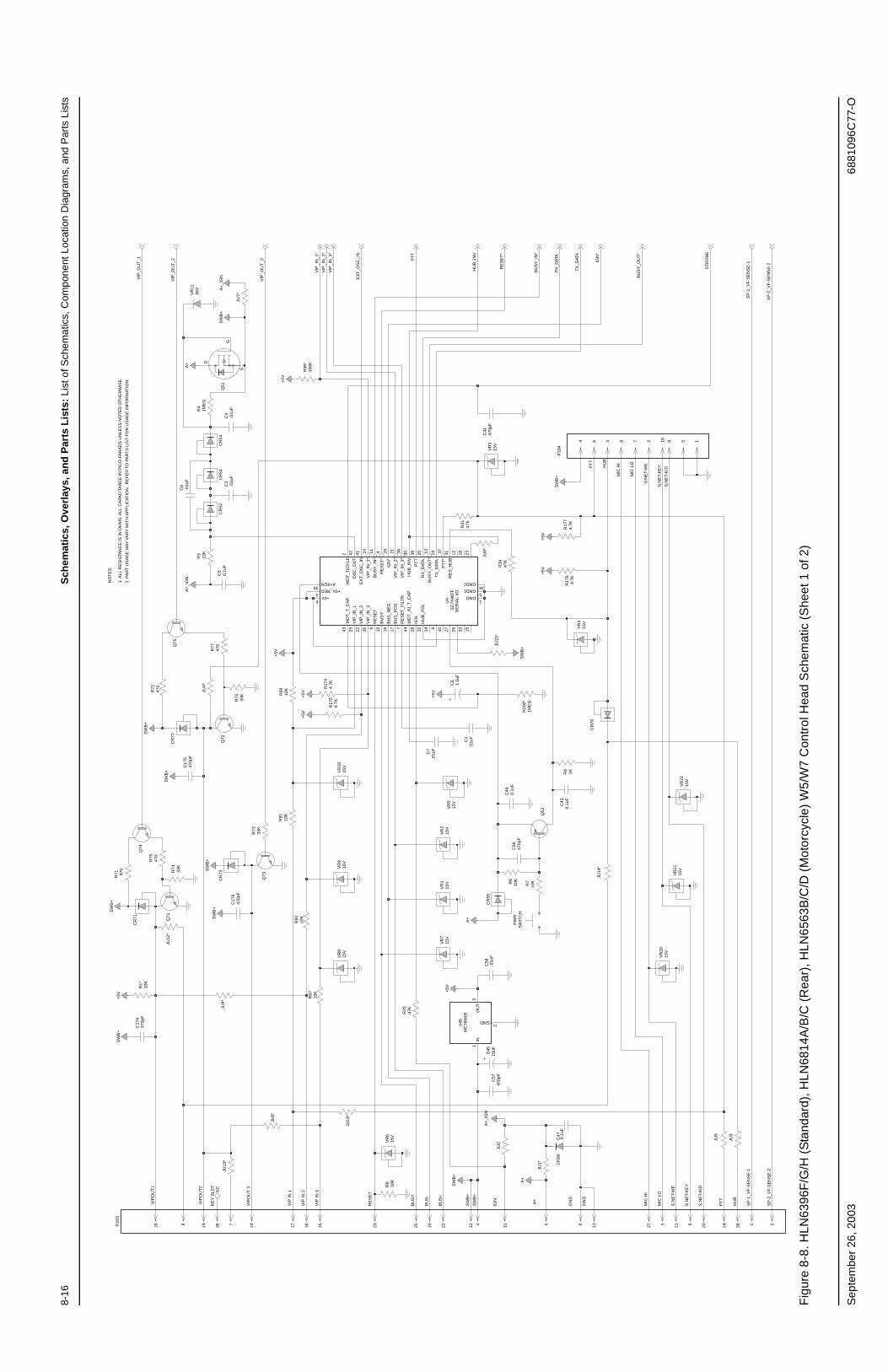
8-16
Sch
emat
ics,
Ove
rlay
s, a
nd
Par
ts L
ists
: Li
st o
f Sch
emat
ics,
Com
pone
nt L
ocat
ion
Dia
gram
s, a
nd P
arts
Lis
ts
Sep
tem
ber
26, 2
003
6881
096C
77-O
Fig
ure
8-8.
HLN
6396
F/G
/H (
Sta
ndar
d), H
LN68
14A
/B/C
(R
ear)
, HLN
6563
B/C
/D (
Mot
orcy
cle)
W5/
W7
Con
trol
Hea
d S
chem
atic
(S
heet
1 o
f 2)
VIP
IN 1
KE
Y S
LOT
2. P
AR
T U
SA
GE
MAY
VA
RY
WIT
H A
PP
LIC
ATIO
N.
RE
FE
R T
O P
AR
TS
LIS
T F
OR
US
AG
E IN
FO
RM
ATIO
N.
SE
RIA
L I/O
NO
TE
S:
BU
S-
RE
SE
T
VIP
IN 3
MIC
HI
S.N
ET-
WE
PT
T
VIP
IN 2
GN
D
S.N
ET-
KID
SW
B+
GN
D
VIP
OU
T1
S.N
ET-
KE
Y
P10
3
MIC
LO
VIP
OU
T 3
1. A
LL R
ES
ISTA
NC
E IS
IN O
HM
S. A
LL C
APA
CIT
AN
CE
IN P
ICO
-FA
RA
DS
UN
LES
S N
OT
ED
OT
HE
RW
ISE
.
A+
SW
B+
G
S
DV
IPO
UT
2
S.N
ET-
WE
BU
SY
IGN
BU
S+
SW
B+
S.N
ET-
KID
S.N
ET-
KE
Y
P10
4
MIC
HI
MIC
LO
HU
B
PT
T
HU
B
SP
-1_V
F-S
EN
SE
-1
SP
-2_V
F-S
EN
SE
-2
Q71 SW
B+
470p
FC
176
CR
90
VR
515
V
SW
B+
A+
_IG
N
15V
VR
3
10K
R6
JU2
CR
52
8 7
SW
B+
3
0.1u
F
C17
447
0pF
+5V
C47
SW
B+
C6
1.5u
F
6 35 13114
C7
.01u
F
470p
FC
41
47K
R34
+5V
4.7K
R17
7
CR
76
VR
4
C4
.01u
F
15V
R87
10K
CR
71
Q73
+5V
+5V
C17
547
0pF
2223 10 1225
2
15
JU4*
10K
A+
R20
0*
R99
1ME
G
47K
R31
4.7K
R17
6VIP
_IN
_3*
36
WD
T_I
N_T
_CA
P44
WD
T_T
ICK
LE2
WD
T_T
_CA
P43
+5V
RE
S_H
UB
31
RX
_DAT
A20
TX
_DAT
A19
VIP
_IN
_125
VIP
_IN
_222 35
VIP
_IN
_3V
IP_I
N_1
*24
VIP
_IN
_2*
21
OS
C_O
UT
6+5V
+5V_REG3
PT
T38
PT
T*
37
9R
ES
ET
RE
SE
T*
4
7R
ES
ET
_FIL
TR
40 27 26 33 15
12 18 2342
5GND1
34GND2
HU
B_I
NV
30
HU
B_P
OL
32IG
N28
IGN
*29
14 8
39
BU
SY
10B
US
Y_I
N*
11
BU
SY
_OU
T*
13
BU
S_N
EG
16 17B
US
_PO
S
41E
XT
_OS
C_I
N
GND1
SC
7448
7FU
4
A+/IGN
R98
*10
0K
+5V
JU8*
10uF
C45
7 17 16
VR
10
A+
_IG
N
15V
9
C5
0.1u
F
Q52
22K
R3
CR
53C
3.0
1uF
CR
54
JU15
*
1ME
GR
436
VV
R11
4 6
CR
55A
+_I
GN
A+
33K
R74
JU1*
JU3
SW
B+
R17
54.
7K
SW
B+
1KR8
CR
73
470p
FC
57
10K
R84
R81
10K
33K
R73
R7
10K
.01u
FC
1
R71 47
0
VR
215
V
JU5
15V
VR
1
NC
C48
0.1u
F
C8
.01u
F
SW
B+
PW
RS
WIT
CH
15V
VR
20
15V
VR
21
VR
2215
V
142619
JU9*
JU13
*
1
Q74
10 5
R77
470
R76
470
33K
R75
JU18
*
470
R72
U45 GND
2
IN1
OU
T3
+5V
+5V
C58
.01u
F
MC
78M
05
JU7*
15V
8
VR
9
18
R1*
10K
C43
0.1u
F
15V
VR
6R
910
K
SW
B+
4.7K
R17
4
JU14
*
15V
VR
8
C56
470p
F
+5V
Q75
JU6*
47K
R25
SW
B+
CR
72
15V
VR
7
Q72
Q51
A+
JU12
*
124 29 2821 20
VIP
_OU
T_1
ST
RO
BE
EX
T_O
SC
_IN
VIP
_IN
_3*
BU
SY
_OU
T*
IGN
*
TX
_DAT
A
RX
_DAT
A
BU
SY
_IN
*
RE
SE
T*
HU
B_I
NV
PT
T
VIP
_IN
_2*
VIP
_IN
_1*
SP
-1_V
F-S
EN
SE
-1
SP
-2_V
F-S
EN
SE
-2
27
VIP
_OU
T_3
VIP
_OU
T_2

Sch
emat
ics,
Ove
rlay
s, a
nd
Par
ts L
ists
: Li
st o
f Sch
emat
ics,
Com
pone
nt L
ocat
ion
Dia
gram
s, a
nd P
arts
Lis
ts8-
17
6881
096C
77-O
Sep
tem
ber
26, 2
003
Fig
ure
8-9.
HLN
6396
F/G
/H (
Sta
ndar
d),H
LN68
14A
/B/C
(R
ear)
, HLN
6563
B/C
/D (
Mot
orcy
cle)
W5/
W7
Con
trol
Hea
d S
chem
atic
(S
heet
2 o
f 2)
G
S
WAR
NIN
G!
(RED
)(Y
ELLO
W)
VF D
ISPL
AY
DAM
AGE
TO T
HE
CIR
CU
IT
DIA
GN
OST
IC T
EST
DO
NO
T PR
OBE
U3
PIN
5
MAY
OC
CU
R.
WIT
H P
OW
ER A
PPLI
ED.
SHO
RT
TO G
ND
. FO
R
SHO
RT
TO D
ISAB
LEKE
YPAD
BAC
KLIG
HT
NO
TES:
1. A
LL R
ESIS
TAN
CE
IS IN
OH
MS.
ALL
CAP
ACIT
ANC
E IN
PIC
O-F
ARAD
S U
NLE
SS N
OTE
D O
THER
WIS
E.2.
PAR
T U
SAG
E M
AY V
ARY
WIT
H A
PPLI
CAT
ION
. R
EFER
TO
PAR
TS L
IST
FOR
USA
GE
INFO
RM
ATIO
N.
BUSY
XMIT
D
3.U
1 PI
NS
3,18
,23,
40 A
RE
NO
T C
ON
NEC
TED
WIT
H M
C68
HC
05C
8A M
ICR
OPR
OC
ESSO
R.
PN624
PO
C36
470p
F
PFPG5
PH20
PI22
PJ7
PK4
PL21
PM19
G6
11G
710
G8
9
PA323
PB PC18
PD8
PE13 2
U10
2
1F1
25F2G
117
G2
16G
315
G4
14G
512
CR
112
32M
01
C23
3013
30pF
C20
470p
F
R57 47K
R29
470p
FC
31
444
VSS22
100K
34
DAT
A_IN
35
CLO
CK
36 37W
DT_
TKL
IGN
*39
RES
ET*
1
BUSY
_IN
*41
STR
OBE
38
VDD VIP_
OU
T_3
28
VIP_
OU
T_2
27 26VI
P_O
UT_
1BU
SY_I
N25 24
RX_
DAT
A32
TX_D
ATA
33
DAT
A_IN
15
PB3
16
PB4
17 19BK
LTIN
V_H
UB
20
PTT
21
VIP_
IN_3
31
VIP_
IN_2
30
VIP_
IN_1
29
PA3
9
PA4
8 7LT
CH
_EN
BLH
V_C
NTR
L6
BUSY
_OU
T*5
PB0
13
PB1
14
PB2
+5V_
FIL
18 23
IGN
*40
OSC
143
OSC
242
PA0
12
PA1
11
PA2
10
SWB+
SWB+
MC
68H
C70
5C8A
U1
2IR
Q*
3
470p
FC
54
C32
470p
F
470p
FC
33
470p
FC
34
4 26
C35
470p
F
470p
FC
30
100K
R12
2R
121
100K
CR
133
CR
134
191817
CR
51
30
26
Q11
1
C12
*
JU10
0*
25
12
100K
JU17
*
R11
2
JU16
4.7K
SWB+
R13
1
R5
100K
+5V
560
R12
3R
124
100K
12
+5V
+5V
C52
10uF
NC
13 2911
HO
ME
SWIT
CH
1014
+5V
470p
F
C38
C18
*
C40
470p
F
22K
R51
R11
433
K
VR24
10V
72
+5V
1
1K
+5V
28
Q11
2
R11
6
470p
FC
37
1231
31
8 4
3231
15 16
C10
1*
212016
U3-
1LM
2903
2
C42
*
22
1uF
C46
272
+5V_
FIL
1
R18
122
K
12
C26
470p
F
.01u
F
SWB+
DIM
SWIT
CH
C19
*
C51
C17
C14
*
470p
FC
R13
2
CR
131
C24
*
14
C55
R52
1000
uF
CR
136
10K
100K
C10
*
9.10
7uH
L50
R12
0
C39
241
470p
F
470p
F
C2
R17
810
K
470p
F
10
L1 9.10
7uH
R2
+5V
C27
1.5KR60
4.7K
9
28
C50
10uF
33K
R11
3
24
1KR11
5
8
100K
R11
1
Y1
6 7
470p
FC
28
FREQ
=4M
Hz
6
12
12R
180
SWIT
CH
VU
1 2
SEL
SWIT
CH
U3-
2LM
2903
6 57
8 4
VR50
25
+5V_
FIL
17235
36V
4 5
R10
112
15
1000
uFC
53
C16
*
C15
*
CR
139
CR
140
560
183 9
R50
CR
135
+5V
CR
138
6.8KR61
2
SWIT
CH
MD
12
MU
SWIT
CH
1 2
OPT
2SW
ITC
H
1
1 2 3
4 5 6
23
77J0
3T6
0
R18
212
+5V
C29
470p
F
10
R56
33K
C44
*
30pF
+5V
8
C22
11
+5V_
FIL
C11
*
342
24LT
CH
_EN
BL VCC1 44
VDISP 1
CR
137
54Q
31Q
323
Q4
39Q
538
Q6
37Q
736
Q8
35Q
9
1312Q
24Q
2511
Q26
10Q
279
Q28
8Q
297
Q3
40
Q30
2520Q
17Q
1819
Q19
17 41Q
2
16Q
20Q
2115
Q22
14Q
23
29
42Q
1
Q10
33Q
1132
Q12
3130Q
13Q
1427
Q15
26Q
16
STR
OBE
21 23C
LK
DAT
A_IN
43
GND22
6N
C1
NC
218
NC
328
NC
4
12
2729
U10
1
UC
Q58
18EP
F
SWIT
CH
OPT
4
1 2
SWIT
CH
OPT
3
SWB+
R55
1MEGR30
+5V
12
R59
22
C25
*
10K
C21
3
0.1u
FC
13
470p
F
C9*
JU19
Q13
1
R58
1K
20
33K
R28
CR
111
Q50
1 2
1932 21
S7
1 2
SWIT
CH
S8
1 2
SWIT
CH
S6
12
SWIT
CH
1 2
SWIT
CH
S1SW
ITC
HS4
1 2
SWIT
CH
S3
2
SWIT
CH
S5
1 2
SWIT
CH
12
SWIT
CH
S2
1
SWIT
CH
STAR
1 2
PND
2
SWIT
CH
OPT
1
1 2
SWIT
CH
1 2
SWIT
CH
VD
1
SWIT
CH
S0
1 2
S9
G5
G4
G3
G2
G1 R Y
PBPF PA PK PG PN PJ PO
DAT
A_INCLK
STR
OBE
VIP_
IN_1
*
VIP_
IN_2
*
VIP_
OU
T_3
SP-1
_VF-
SEN
SE-1
EXT_
OSC
_IN
HU
B_IN
VPT
T
STR
OBE
CLO
CK
RX_
DAT
ATX
_DAT
A
VIP_
IN_3
*
SP-2
_VF-
SEN
SE-2
G8
P0VDIS
P
LTC
H_E
NBL
PD PE PM PH PC PLG8
G7
G6
PI
BUS3(32:1)
VDIS
P
IGN
*
RES
ET*
DAT
A_IN
BUSY
_IN
*
LTC
H_E
NBL
VIP_
OU
T_1
VIP_
OU
T_2
BKLT
STR
OBE
BUSY
_OU
T*
G7
G6
G5
G4
G3
G2
G1
G8
F2F1YR
PBP0F2 PI PL PH PM PC PE PD PJ PN PG PK PA PF F1
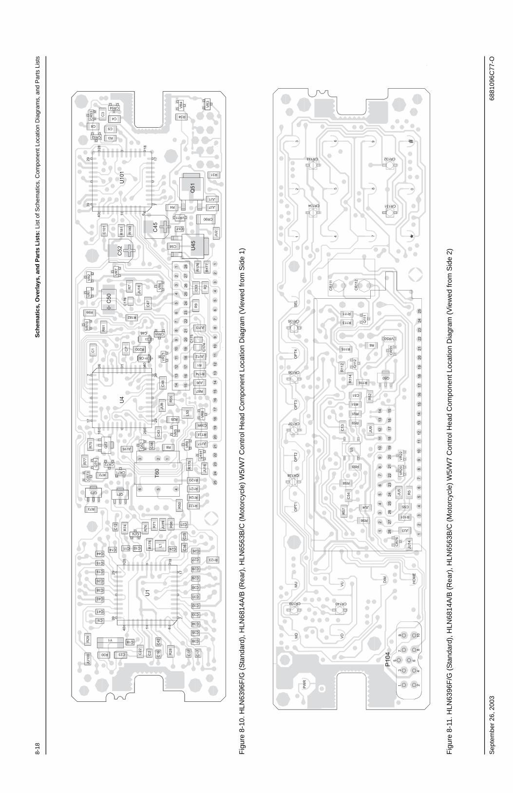
8-18
Sch
emat
ics,
Ove
rlay
s, a
nd
Par
ts L
ists
: Li
st o
f Sch
emat
ics,
Com
pone
nt L
ocat
ion
Dia
gram
s, a
nd P
arts
Lis
ts
Sep
tem
ber
26, 2
003
6881
096C
77-O
Fig
ure
8-10
. HLN
6396
F/G
(S
tand
ard)
, HLN
6814
A/B
(R
ear)
, HLN
6563
B/C
(M
otor
cycl
e) W
5/W
7 C
ontr
ol H
ead
Com
pone
nt L
ocat
ion
Dia
gram
(V
iew
ed fr
om S
ide
1)
Fig
ure
8-11
. HLN
6396
F/G
(S
tand
ard)
, HLN
6814
A/B
(R
ear)
, HLN
6563
B/C
(M
otor
cycl
e) W
5/W
7 C
ontr
ol H
ead
Com
pone
nt L
ocat
ion
Dia
gram
(V
iew
ed fr
om S
ide
2)
JU10
0R
29 C39
C9
C41
C40
C38
C20
C19
C15
C44C14 C11 C10
Q74
C24
C21
R123
C23R30
C18Y1
R122
R124
R121
R120
C35
C34
C33
C32
C31
C30
C29
C28
C27
C26
C22
C2
C16
C42
R28
C37
C17
7
7
6
6
1
1
17
17
U1
40
40
39
39
29
29
28
28
18
18
12
34
56
78
910
1112
1314
12
34
56
78
910
1112
1314
2827
2625
25
24
24
23
23
22
22
21
21
20
20
19
19
18
18
17
17
16
16
15
15
T60
U4
U10
1
Q51
U45
C45
C52
C50
JU17
R131
C39RR25
R87
JU6
R174
R1
JU12
JU13
C17
5
C17
4
CR90
JU7
JU1
R31
R4
R3
C5
C4
C8
CR52
CR54
R34
C58
VR11
C57
CR55C46
C6
R200
R182R99
R8JU15
CR71
Q71
CR72
R72
Q73
R73
VR4
VR3
C3
CR
53
JU2
R17
7R
2
C53
R9
VR6
C47
JU18R
7C
176
R81
C1
VR10
VR1
VR2 VR
7
C7
VR21
C48
R55
JU8
L50
VR8
VR9
VR5
C43
C56
Q52Q72
R75
R77
CR
73
Q75
R17
5
JU16
Q13
1
R50
R98
C25
C36L1R
178
JU19
R71
R76R74C12
R17
6
R18
0
R18
1
C10
1
7
61
17
40
3929
28 18
1236 5 4
R113
R111
R115
R116Q50
R59
R60
R58
JU4
R101
JU3
R56
R61
R51
C51
VR50
R6
*#
VR22
VR20
C55
CR
76
JU14
JU5
R5
PWR
MD
MU VU
VD
DIM
HO
ME
OPT
1O
PT2
OPT
3O
PT4
SEL
C54
R57
P104
U3
JU9
C13
R52
R11
4
R11
2 Q11
2
CR
51
Q11
1
CR
111
CR
112
12
34
56
78
910
1112
1314
2827
2625
2423
2221
2019
1817
1615
1
1
22
3
3
44
5
5
66
7
7
88
9
9
1010
1112
1314
2524
2322
2120
1918
1716
15
CR138
CR139 CR140
CR137
CR136
CR135
CR134
CR133
CR131
CR132
12
3
45
6
78
9
0
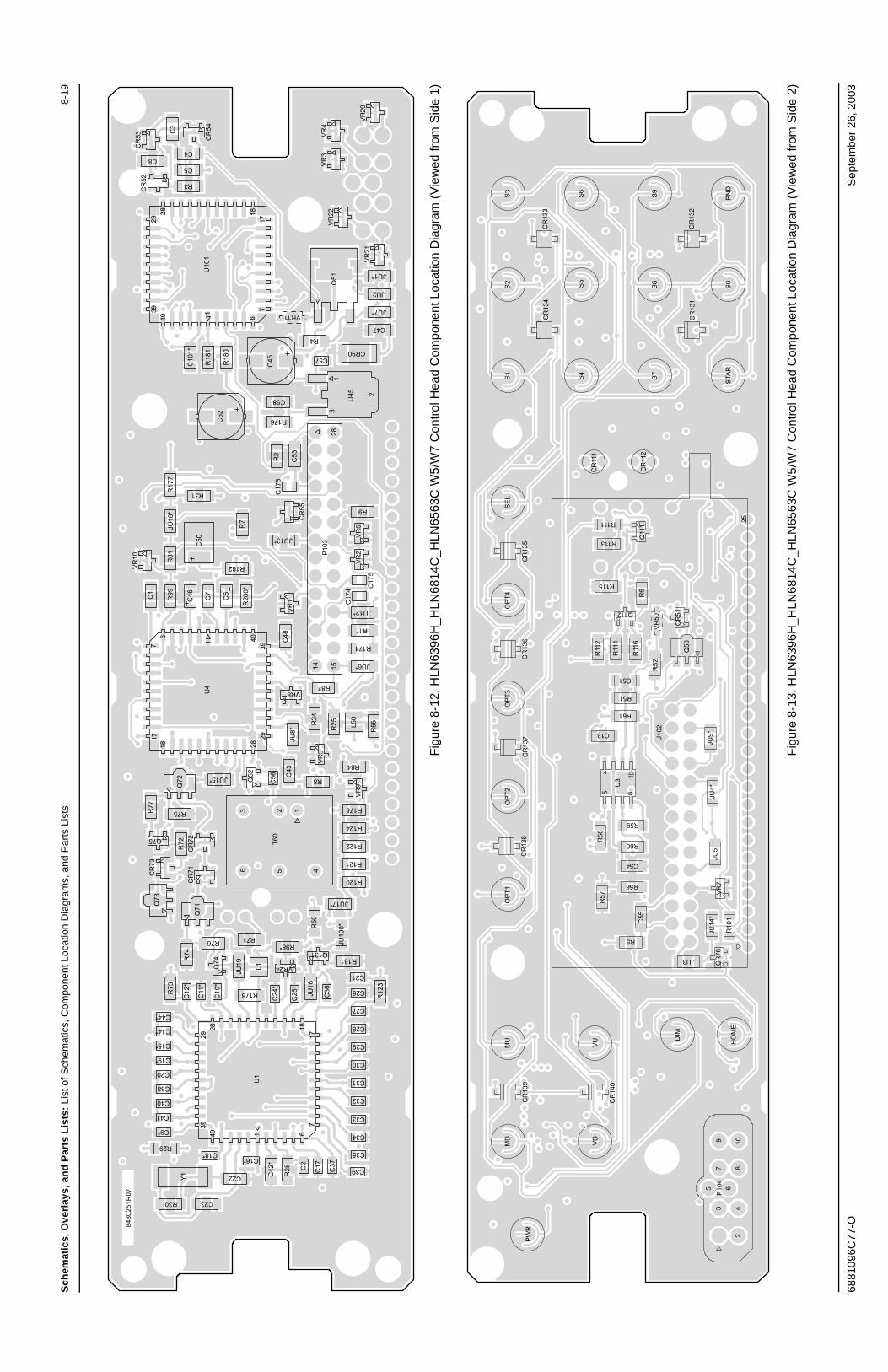
Sch
emat
ics,
Ove
rlay
s, a
nd
Par
ts L
ists
: Li
st o
f Sch
emat
ics,
Com
pone
nt L
ocat
ion
Dia
gram
s, a
nd P
arts
Lis
ts8-
19
6881
096C
77-O
Sep
tem
ber
26, 2
003
Fig
ure
8-12
. HLN
6396
H_H
LN68
14C
_HLN
6563
C W
5/W
7 C
ontr
ol H
ead
Com
pone
nt L
ocat
ion
Dia
gram
(V
iew
ed fr
om S
ide
1)
Fig
ure
8-13
. HLN
6396
H_H
LN68
14C
_HLN
6563
C W
5/W
7 C
ontr
ol H
ead
Com
pone
nt L
ocat
ion
Dia
gram
(V
iew
ed fr
om S
ide
2)
C1
C2
C3
C4
C5
C6
C7
C8
C17
C10
*
C10
1*C
11*
C12
*
C14*
C15*
C16*C18*
C19*
C20
C21
C22
C23
C26
C27
C28
C29
C24
*
C25
*
C30
C31
C32
C33
C34
C35
C36
C37
C38
C39
C40
C41
C43
C45
C46
C47
C48
C42
*
C44*
C50
C52
C53
C56
C57
C58
C17
4 C17
5
C17
6
C9*
CR
52C
R53 CR
54
CR
55
CR
71C
R72
CR
73
CR90
JU2
JU1*
JU16
JU19
JU10
0*
JU12*
JU13*
JU15*
JU17*
JU18
*
JU6*
JU7*
JU8*
L1
L50
1514
28P1
03Q
51
Q52
Q71
Q72
Q73
Q74
Q75
Q131
R2
R3
R4
R7
R8
R9
R1*
R25
R28
R29
R20
0*
R30
R31
R34
R50
R55
R71
R72
R73
R74
R75
R76
R77
R81
R84
R87
R99
R120
R121
R122
R12
3
R124
R131
R174
R175
R176
R17
7
R178
R18
0
R18
1
R182
R98*
4563 2 1
T60
64039
2928 18
177
1U
1
1
67
1718 28
2939
40
U4
3
2
1
U45
1
67
171828
2939
40
U10
1
VR1
VR2
VR3
VR4
VR5
VR6
VR8
VR9
VR10
VR11
VR20
VR21
VR22
VR24
Y1
8480
251R
07
C13
C51
C54
C55
CR
51
CR
76
CR
111
CR
112
CR
131
CR
132
CR
133
CR
134
CR
135
CR
136
CR
137
CR
138
CR
139
CR
140
DIM
HO
ME
JU3
JU5
JU14
*JU
4*JU
9*
MD
MU
OPT
1O
PT2
OPT
3O
PT4
35 6
7 84
2
9 10
P104
PND
PWR
Q50
Q11
1
Q112
R5
R6
R51
R52
R56
R57
R58
R59
R60
R61
R10
1
R111
R11
2
R113
R11
4
R115
R11
6
S0
S1S2
S3
S4S5
S6
S7S8
S9
SEL
STAR
145 8
U3
25
U10
2
VD
VR7
VR50
VU

8-20
Sch
emat
ics,
Ove
rlay
s, a
nd
Par
ts L
ists
: Li
st o
f Sch
emat
ics,
Com
pone
nt L
ocat
ion
Dia
gram
s, a
nd P
arts
Lis
ts
Sep
tem
ber
26, 2
003
6881
096C
77-O
HL
N63
96H
Sta
nd
ard
Par
ts L
ist
ITE
MM
OT
OR
OL
A
PA
RT
N
UM
BE
RD
ES
CR
IPT
ION
C00
5321
1374
1N21
CA
P C
HIP
CL2
X7R
10%
100
0
C00
5521
1374
1N21
CA
P C
HIP
CL2
X7R
10%
100
0
C1
2113
741N
45C
AP
CH
IP C
L2 X
7R 1
0% 1
0000
C10
NO
TP
LAC
ED
64A
M D
UM
MY
PA
RT
NU
MB
ER
C10
1N
OT
PLA
CE
D64
AM
DU
MM
Y P
AR
T N
UM
BE
R
C11
NO
TP
LAC
ED
64A
M D
UM
MY
PA
RT
NU
MB
ER
C12
NO
TP
LAC
ED
64A
M D
UM
MY
PA
RT
NU
MB
ER
C13
2113
741N
69C
AP
CH
IP C
L2 X
7R 1
0%
1000
00
C14
NO
TP
LAC
ED
64A
M D
UM
MY
PA
RT
NU
MB
ER
C15
NO
TP
LAC
ED
64A
M D
UM
MY
PA
RT
NU
MB
ER
C16
NO
TP
LAC
ED
64A
M D
UM
MY
PA
RT
NU
MB
ER
C17
2113
741M
13C
AP
CH
IP C
L2 X
7R 1
0% 4
70
C17
421
1374
1M13
CA
P C
HIP
CL2
X7R
10%
470
C17
521
1374
1M13
CA
P C
HIP
CL2
X7R
10%
470
C17
621
1374
1M13
CA
P C
HIP
CL2
X7R
10%
470
C18
NO
TP
LAC
ED
64A
M D
UM
MY
PA
RT
NU
MB
ER
C19
NO
TP
LAC
ED
64A
M D
UM
MY
PA
RT
NU
MB
ER
C2
2113
741M
13C
AP
CH
IP C
L2 X
7R 1
0% 4
70
C20
2113
741M
13C
AP
CH
IP C
L2 X
7R 1
0% 4
70
C21
2113
741M
13C
AP
CH
IP C
L2 X
7R 1
0% 4
70
C22
2113
740B
36C
AP
CH
IP R
EE
L C
L1 +
/-30
30
C23
2113
740B
36C
AP
CH
IP R
EE
L C
L1 +
/-30
30
C24
NO
TP
LAC
ED
64A
M D
UM
MY
PA
RT
NU
MB
ER
C25
NO
TP
LAC
ED
64A
M D
UM
MY
PA
RT
NU
MB
ER
C26
2113
741M
13C
AP
CH
IP C
L2 X
7R 1
0% 4
70
C27
2113
741M
13C
AP
CH
IP C
L2 X
7R 1
0% 4
70
C28
2113
741M
13C
AP
CH
IP C
L2 X
7R 1
0% 4
70
C29
2113
741M
13C
AP
CH
IP C
L2 X
7R 1
0% 4
70
C3
2113
741N
45C
AP
CH
IP C
L2 X
7R 1
0% 1
0000
C30
2113
741M
13C
AP
CH
IP C
L2 X
7R 1
0% 4
70
C31
2113
741M
13C
AP
CH
IP C
L2 X
7R 1
0% 4
70
C32
2113
741M
13C
AP
CH
IP C
L2 X
7R 1
0% 4
70
C33
2113
741M
13C
AP
CH
IP C
L2 X
7R 1
0% 4
70
C34
2113
741M
13C
AP
CH
IP C
L2 X
7R 1
0% 4
70
C35
2113
741M
13C
AP
CH
IP C
L2 X
7R 1
0% 4
70
C36
2113
741M
13C
AP
CH
IP C
L2 X
7R 1
0% 4
70
C37
2113
741M
13C
AP
CH
IP C
L2 X
7R 1
0% 4
70
C38
2113
741M
13C
AP
CH
IP C
L2 X
7R 1
0% 4
70
C39
2113
741M
13C
AP
CH
IP C
L2 X
7R 1
0% 4
70
C4
2113
741N
45C
AP
CH
IP C
L2 X
7R 1
0% 1
0000
C40
2113
741M
13C
AP
CH
IP C
L2 X
7R 1
0% 4
70
C41
2113
741M
13C
AP
CH
IP C
L2 X
7R 1
0% 4
70
C42
NO
TP
LAC
ED
64A
M D
UM
MY
PA
RT
NU
MB
ER
C43
2113
741N
69C
AP
CH
IP C
L2 X
7R 1
0%
1000
00
C44
NO
TP
LAC
ED
64A
M D
UM
MY
PA
RT
NU
MB
ER
C45
2380
090M
24C
AP
ALU
10
20 5
0V S
UR
F M
T
C46
2311
049A
37C
AP
TA
NT
CH
IP 1
20
20
C47
2113
741N
69C
AP
CH
IP C
L2 X
7R 1
0%
1000
00
C48
2113
741N
69C
AP
CH
IP C
L2 X
7R 1
0%
1000
00
C5
2113
741N
69C
AP
CH
IP C
L2 X
7R 1
0%
1000
00
C50
2311
049A
95C
AP
TA
NT
CH
IP 1
0 U
F 2
5V
10%
C51
2113
741N
45C
AP
CH
IP C
L2 X
7R 1
0% 1
0000
C52
2380
090M
24C
AP
ALU
10
20 5
0V S
UR
F M
T
C54
2113
740B
65C
AP
CH
IP R
EE
L C
L1 +
/-30
470
C56
2113
741M
13C
AP
CH
IP C
L2 X
7R 1
0% 4
70
C57
2113
741M
13C
AP
CH
IP C
L2 X
7R 1
0% 4
70
C58
2113
741N
45C
AP
CH
IP C
L2 X
7R 1
0% 1
0000
C6
2311
049A
38C
AP
TA
NT
CH
IP 1
.5 1
0 16
C7
2113
741N
45C
AP
CH
IP C
L2 X
7R 1
0% 1
0000
C8
2113
741N
45C
AP
CH
IP C
L2 X
7R 1
0% 1
0000
C9
NO
TP
LAC
ED
64A
M D
UM
MY
PA
RT
NU
MB
ER
CR
111
4880
026P
01D
IOD
E L
ED
RE
D
CR
112
4880
026P
02D
IOD
E L
ED
YE
LLO
W
ITE
MM
OTO
RO
LA
P
AR
T
NU
MB
ER
DE
SC
RIP
TIO
N
CR
131
4880
052R
03D
IOD
E L
IGH
T E
MIT
TIN
G G
RN
CR
132
4880
052R
03D
IOD
E L
IGH
T E
MIT
TIN
G G
RN
CR
133
4880
052R
03D
IOD
E L
IGH
T E
MIT
TIN
G G
RN
CR
134
4880
052R
03D
IOD
E L
IGH
T E
MIT
TIN
G G
RN
CR
135
4880
052R
03D
IOD
E L
IGH
T E
MIT
TIN
G G
RN
CR
136
4880
052R
03D
IOD
E L
IGH
T E
MIT
TIN
G G
RN
CR
137
4880
052R
03D
IOD
E L
IGH
T E
MIT
TIN
G G
RN
CR
138
4880
052R
03D
IOD
E L
IGH
T E
MIT
TIN
G G
RN
CR
139
4880
052R
03D
IOD
E L
IGH
T E
MIT
TIN
G G
RN
CR
140
4880
052R
03D
IOD
E L
IGH
T E
MIT
TIN
G G
RN
CR
5148
1105
8B11
DIO
DE
48S
1105
8A11
A/P
CR
5248
1105
8B11
DIO
DE
48S
1105
8A11
A/P
CR
5348
1105
8B11
DIO
DE
48S
1105
8A11
A/P
CR
5448
1105
8B11
DIO
DE
48S
1105
8A11
A/P
CR
5548
1105
8B11
DIO
DE
48S
1105
8A11
A/P
CR
7148
1105
8B11
DIO
DE
48S
1105
8A11
A/P
CR
7248
1105
8B11
DIO
DE
48S
1105
8A11
A/P
CR
7348
1105
8B11
DIO
DE
48S
1105
8A11
A/P
CR
7648
1105
8B11
DIO
DE
48S
1105
8A11
A/P
CR
9048
8296
0R02
DIO
DE
RE
CT
48R
8296
0R01
A/P
JU00
0306
1107
7A01
RE
S C
HIP
JU
MP
ER
JU00
0506
1107
7A01
RE
S C
HIP
JU
MP
ER
JU00
1606
1107
7A01
RE
S C
HIP
JU
MP
ER
JU00
17N
OT
PLA
CE
D64
AM
DU
MM
Y P
AR
T N
UM
BE
R
JU1
NO
TP
LAC
ED
64A
M D
UM
MY
PA
RT
NU
MB
ER
JU10
0N
OT
PLA
CE
D64
AM
DU
MM
Y P
AR
T N
UM
BE
R
JU12
NO
TP
LAC
ED
64A
M D
UM
MY
PA
RT
NU
MB
ER
JU13
NO
TP
LAC
ED
64A
M D
UM
MY
PA
RT
NU
MB
ER
JU14
NO
TP
LAC
ED
64A
M D
UM
MY
PA
RT
NU
MB
ER
JU15
NO
TP
LAC
ED
64A
M D
UM
MY
PA
RT
NU
MB
ER
JU18
NO
TP
LAC
ED
64A
M D
UM
MY
PA
RT
NU
MB
ER
JU19
NO
TP
LAC
ED
64A
M D
UM
MY
PA
RT
NU
MB
ER
JU2
0611
077A
01R
ES
CH
IP J
UM
PE
R
ITE
MM
OTO
RO
LA
PA
RT
N
UM
BE
RD
ES
CR
IPT
ION
JU4
NO
TP
LAC
ED
64A
M D
UM
MY
PA
RT
NU
MB
ER
JU6
NO
TP
LAC
ED
64A
M D
UM
MY
PA
RT
NU
MB
ER
JU7
NO
TP
LAC
ED
64A
M D
UM
MY
PA
RT
NU
MB
ER
JU8
NO
TP
LAC
ED
64A
M D
UM
MY
PA
RT
NU
MB
ER
JU9
NO
TP
LAC
ED
64A
M D
UM
MY
PA
RT
NU
MB
ER
L124
8014
0E16
IND
UC
TO
R C
HIP
10U
H
L50
2480
140E
16IN
DU
CT
OR
CH
IP 1
0UH
MP
0103
4380
290L
01S
PA
CE
R L
ED
MP
0106
5480
004N
01LA
BE
L B
AR
CO
DE
P01
0328
8010
2M07
PLU
G V
ER
TIC
AL
28 P
OS
ITIO
N
P01
0428
8006
8M01
HE
AD
ER
MIC
Q11
148
8014
1L02
TS
TR
NP
N S
OT
23 L
O P
RO
FIL
E
TAP
E
Q11
248
8014
1L02
TS
TR
NP
N S
OT
23 L
O P
RO
FIL
E
TAP
E
Q13
148
8014
1L02
TS
TR
NP
N S
OT
23 L
O P
RO
FIL
E
TAP
E
Q50
4880
053M
03T
ST
R N
/CH
SO
T 8
9 20
0V B
ST
84
Q51
4813
821A
30M
OS
FE
T N
-CH
60V
15A
Q52
4880
141L
01T
ST
R P
NP
SO
T23
LO
PR
OF
ILE
TA
PE
Q71
4880
053M
02T
ST
R N
PN
MX
T22
22A
Q72
4880
053M
02T
ST
R N
PN
MX
T22
22A
Q73
4880
053M
02T
ST
R N
PN
MX
T22
22A
Q74
4880
141L
02T
ST
R N
PN
SO
T23
LO
PR
OF
ILE
TA
PE
Q75
4880
141L
02T
ST
R N
PN
SO
T23
LO
PR
OF
ILE
TA
PE
R00
0206
1107
7A90
RE
S C
HIP
470
0 5
1/8
R00
0506
1107
7A90
RE
S C
HIP
470
0 5
1/8
R1
NO
TP
LAC
ED
64A
M D
UM
MY
PA
RT
NU
MB
ER
R10
106
1107
7A28
RE
S C
HIP
12
5 1/
8W
R11
106
1107
7B23
RE
S C
HIP
100
K 5
1/8
W
R11
206
1107
7B23
RE
S C
HIP
100
K 5
1/8
W
R11
306
1107
7B11
RE
S C
HIP
33K
5 1
/8W
ITE
MM
OT
OR
OL
A
PAR
T
NU
MB
ER
DE
SC
RIP
TIO
N

Sch
emat
ics,
Ove
rlay
s, a
nd
Par
ts L
ists
: Li
st o
f Sch
emat
ics,
Com
pone
nt L
ocat
ion
Dia
gram
s, a
nd P
arts
Lis
ts8-
21
6881
096C
77-O
Sep
tem
ber
26, 2
003
R11
406
1107
7B11
RE
S C
HIP
33K
5 1
/8W
R11
506
1107
7A74
RE
S C
HIP
100
0 5
1/8
R11
606
1107
7A74
RE
S C
HIP
100
0 5
1/8
R12
006
1107
7B23
RE
S C
HIP
100
K 5
1/8
W
R12
106
1107
7B23
RE
S C
HIP
100
K 5
1/8
W
R12
206
1107
7B23
RE
S C
HIP
100
K 5
1/8
W
R12
306
1107
7B23
RE
S C
HIP
100
K 5
1/8
W
R12
406
1107
7B23
RE
S C
HIP
100
K 5
1/8
W
R13
106
1107
7A68
RE
S C
HIP
560
5 1
/8W
R17
406
1107
7A90
RE
S C
HIP
470
0 5
1/8
R17
506
1107
7A90
RE
S C
HIP
470
0 5
1/8
R17
606
1107
7A90
RE
S C
HIP
470
0 5
1/8
R17
706
1107
7A90
RE
S C
HIP
470
0 5
1/8
R17
806
1107
7A98
RE
S C
HIP
10K
5 1
/8W
R18
006
1107
7A28
RE
S C
HIP
12
5 1/
8W
R18
106
1107
7B07
RE
S C
HIP
22K
5 1
/8W
R18
206
1107
7A28
RE
S C
HIP
12
5 1/
8W
R20
006
1107
7B47
RE
S C
HIP
1 M
EG
5 1
/8W
R25
0611
077B
15R
ES
CH
IP 4
7K 5
1/8
W
R28
0611
077A
74R
ES
CH
IP 1
000
5 1/
8
R29
0611
077B
23R
ES
CH
IP 1
00K
5 1
/8W
R3
0611
077B
07R
ES
CH
IP 2
2K 5
1/8
W
R30
0611
077B
47R
ES
CH
IP 1
ME
G 5
1/8
W
R31
0611
077B
15R
ES
CH
IP 4
7K 5
1/8
W
R34
0611
077B
15R
ES
CH
IP 4
7K 5
1/8
W
R4
0611
077B
47R
ES
CH
IP 1
ME
G 5
1/8
W
R50
0611
077A
68R
ES
CH
IP 5
60 5
1/8
W
R51
0611
077B
07R
ES
CH
IP 2
2K 5
1/8
W
R52
0611
077A
98R
ES
CH
IP 1
0K 5
1/8
W
R55
0611
077A
28R
ES
CH
IP 1
2 5
1/8W
R56
0611
077B
11R
ES
CH
IP 3
3K 5
1/8
W
R57
0611
077B
15R
ES
CH
IP 4
7K 5
1/8
W
R58
0611
077B
11R
ES
CH
IP 3
3K 5
1/8
W
ITE
MM
OTO
RO
LA
PA
RT
N
UM
BE
RD
ES
CR
IPT
ION
R59
0611
077A
98R
ES
CH
IP 1
0K 5
1/8
W
R6
0611
077A
98R
ES
CH
IP 1
0K 5
1/8
W
R60
0611
077A
78R
ES
CH
IP 1
500
5 1/
8
R61
0611
077A
94R
ES
CH
IP 6
.8K
5 1
/8
R7
0611
077A
98R
ES
CH
IP 1
0K 5
1/8
W
R71
0611
077A
66R
ES
CH
IP 4
70 5
1/8
W
R72
0611
077A
66R
ES
CH
IP 4
70 5
1/8
W
R73
0611
077B
11R
ES
CH
IP 3
3K 5
1/8
W
R74
0611
077B
11R
ES
CH
IP 3
3K 5
1/8
W
R75
0611
077B
11R
ES
CH
IP 3
3K 5
1/8
W
R76
0611
077A
66R
ES
CH
IP 4
70 5
1/8
W
R77
0611
077A
66R
ES
CH
IP 4
70 5
1/8
W
R8
0611
077A
74R
ES
CH
IP 1
000
5 1/
8
R81
0611
077A
98R
ES
CH
IP 1
0K 5
1/8
W
R87
0611
077A
98R
ES
CH
IP 1
0K 5
1/8
W
R9
0611
077A
98R
ES
CH
IP 1
0K 5
1/8
W
R98
NO
TP
LAC
ED
64A
M D
UM
MY
PA
RT
NU
MB
ER
R99
0611
077A
98R
ES
CH
IP 1
0K 5
1/8
W
U01
0272
8003
2M01
DS
PLY
VF
14
SE
G 8
CH
AR
B
LUG
RN
U1
0104
002J
91P
RG
MD
MIC
RO
P A
SS
EM
U10
151
8023
6C05
IC V
F D
RV
R S
N75
518F
N
U3
5113
820A
02IC
DU
AL
SIN
G S
PLY
LO
PW
R
2903
U4
5180
057S
04“I
C C
US
T S
ER
I/O
13”
” R
EE
L”
U45
5113
816G
04IC
+5V
RE
G 7
8M05
VR
0011
4813
830C
41D
IOD
E 3
6V ‘M
3’ M
MS
Z52
58B
T1
VR
0848
1383
0A28
DIO
DE
15V
5%
225
MW
M
MB
Z52
45B
_
VR
0948
1383
0A28
DIO
DE
15V
5%
225
MW
M
MB
Z52
45B
_
VR
148
1383
0A28
DIO
DE
15V
5%
225
MW
M
MB
Z52
45B
_
VR
1048
1383
0A28
DIO
DE
15V
5%
225
MW
M
MB
Z52
45B
_
ITE
MM
OT
OR
OL
A
PAR
T
NU
MB
ER
DE
SC
RIP
TIO
N
VR
248
1383
0A28
DIO
DE
15V
5%
225
MW
M
MB
Z52
45B
_
VR
2048
1383
0A28
DIO
DE
15V
5%
225
MW
M
MB
Z52
45B
_
VR
2148
1383
0A28
DIO
DE
15V
5%
225
MW
M
MB
Z52
45B
_
VR
2248
1383
0A28
DIO
DE
15V
5%
225
MW
M
MB
Z52
45B
_
VR
348
1383
0A28
DIO
DE
15V
5%
225
MW
M
MB
Z52
45B
_
VR
448
1383
0A28
DIO
DE
15V
5%
225
MW
M
MB
Z52
45B
_
VR
548
1383
0A28
DIO
DE
15V
5%
225
MW
M
MB
Z52
45B
_
VR
5048
1383
0C41
DIO
DE
36V
‘M3’
MM
SZ
5258
BT
1
VR
648
1383
0A28
DIO
DE
15V
5%
225
MW
M
MB
Z52
45B
_
VR
748
1383
0A28
DIO
DE
15V
5%
225
MW
M
MB
Z52
45B
_
Y1
4880
065M
01R
ES
ON
TR
CE
RA
MIC
4.0
0 M
HZ
ITE
MM
OT
OR
OL
A
PA
RT
N
UM
BE
RD
ES
CR
IPT
ION
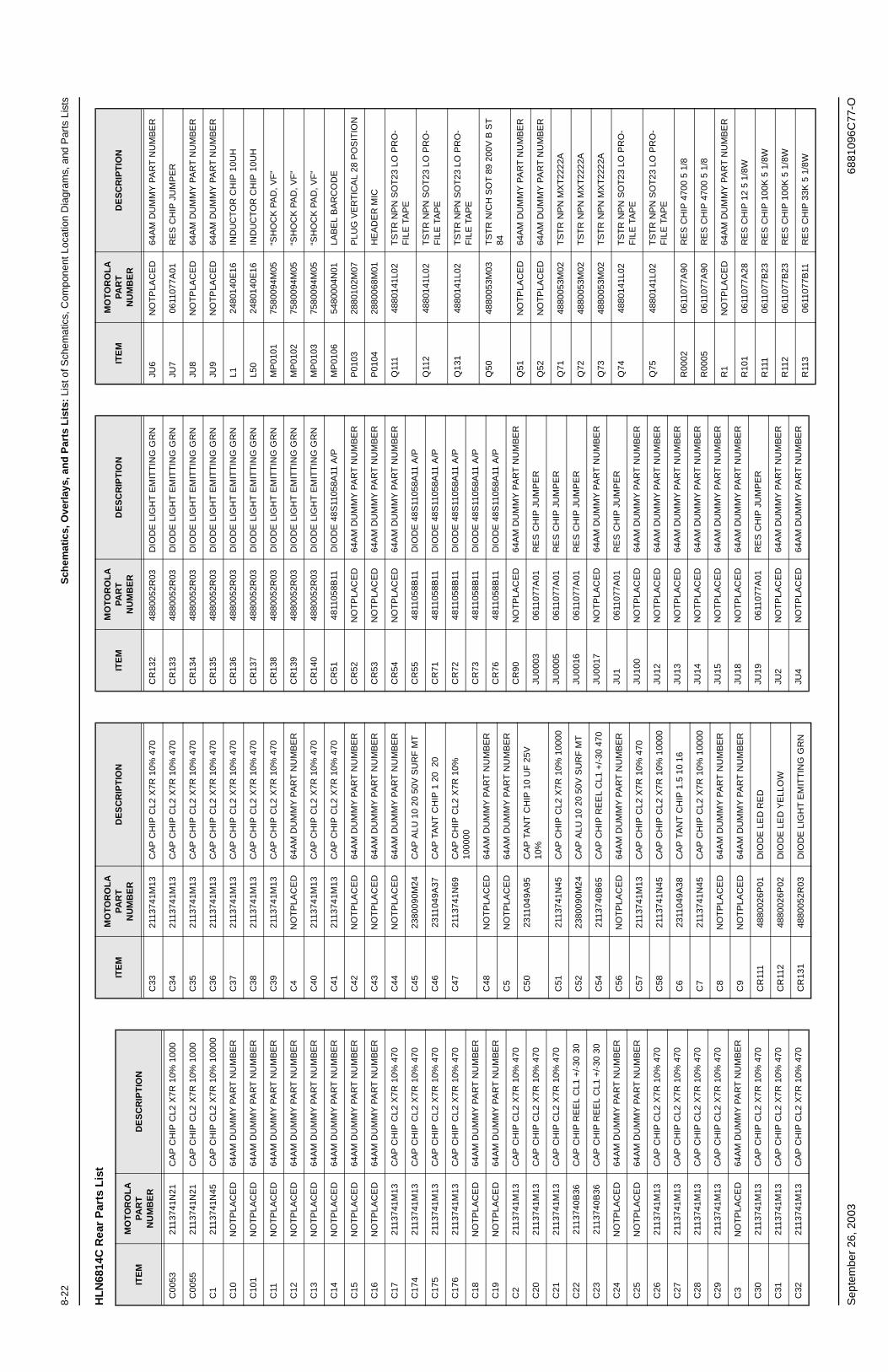
8-22
Sch
emat
ics,
Ove
rlay
s, a
nd
Par
ts L
ists
: Li
st o
f Sch
emat
ics,
Com
pone
nt L
ocat
ion
Dia
gram
s, a
nd P
arts
Lis
ts
Sep
tem
ber
26, 2
003
6881
096C
77-O
HL
N68
14C
Rea
r P
arts
Lis
t
ITE
MM
OT
OR
OL
A
PA
RT
N
UM
BE
RD
ES
CR
IPT
ION
C00
5321
1374
1N21
CA
P C
HIP
CL2
X7R
10%
100
0
C00
5521
1374
1N21
CA
P C
HIP
CL2
X7R
10%
100
0
C1
2113
741N
45C
AP
CH
IP C
L2 X
7R 1
0% 1
0000
C10
NO
TP
LAC
ED
64A
M D
UM
MY
PA
RT
NU
MB
ER
C10
1N
OT
PLA
CE
D64
AM
DU
MM
Y P
AR
T N
UM
BE
R
C11
NO
TP
LAC
ED
64A
M D
UM
MY
PA
RT
NU
MB
ER
C12
NO
TP
LAC
ED
64A
M D
UM
MY
PA
RT
NU
MB
ER
C13
NO
TP
LAC
ED
64A
M D
UM
MY
PA
RT
NU
MB
ER
C14
NO
TP
LAC
ED
64A
M D
UM
MY
PA
RT
NU
MB
ER
C15
NO
TP
LAC
ED
64A
M D
UM
MY
PA
RT
NU
MB
ER
C16
NO
TP
LAC
ED
64A
M D
UM
MY
PA
RT
NU
MB
ER
C17
2113
741M
13C
AP
CH
IP C
L2 X
7R 1
0% 4
70
C17
421
1374
1M13
CA
P C
HIP
CL2
X7R
10%
470
C17
521
1374
1M13
CA
P C
HIP
CL2
X7R
10%
470
C17
621
1374
1M13
CA
P C
HIP
CL2
X7R
10%
470
C18
NO
TP
LAC
ED
64A
M D
UM
MY
PA
RT
NU
MB
ER
C19
NO
TP
LAC
ED
64A
M D
UM
MY
PA
RT
NU
MB
ER
C2
2113
741M
13C
AP
CH
IP C
L2 X
7R 1
0% 4
70
C20
2113
741M
13C
AP
CH
IP C
L2 X
7R 1
0% 4
70
C21
2113
741M
13C
AP
CH
IP C
L2 X
7R 1
0% 4
70
C22
2113
740B
36C
AP
CH
IP R
EE
L C
L1 +
/-30
30
C23
2113
740B
36C
AP
CH
IP R
EE
L C
L1 +
/-30
30
C24
NO
TP
LAC
ED
64A
M D
UM
MY
PA
RT
NU
MB
ER
C25
NO
TP
LAC
ED
64A
M D
UM
MY
PA
RT
NU
MB
ER
C26
2113
741M
13C
AP
CH
IP C
L2 X
7R 1
0% 4
70
C27
2113
741M
13C
AP
CH
IP C
L2 X
7R 1
0% 4
70
C28
2113
741M
13C
AP
CH
IP C
L2 X
7R 1
0% 4
70
C29
2113
741M
13C
AP
CH
IP C
L2 X
7R 1
0% 4
70
C3
NO
TP
LAC
ED
64A
M D
UM
MY
PA
RT
NU
MB
ER
C30
2113
741M
13C
AP
CH
IP C
L2 X
7R 1
0% 4
70
C31
2113
741M
13C
AP
CH
IP C
L2 X
7R 1
0% 4
70
C32
2113
741M
13C
AP
CH
IP C
L2 X
7R 1
0% 4
70
C33
2113
741M
13C
AP
CH
IP C
L2 X
7R 1
0% 4
70
C34
2113
741M
13C
AP
CH
IP C
L2 X
7R 1
0% 4
70
C35
2113
741M
13C
AP
CH
IP C
L2 X
7R 1
0% 4
70
C36
2113
741M
13C
AP
CH
IP C
L2 X
7R 1
0% 4
70
C37
2113
741M
13C
AP
CH
IP C
L2 X
7R 1
0% 4
70
C38
2113
741M
13C
AP
CH
IP C
L2 X
7R 1
0% 4
70
C39
2113
741M
13C
AP
CH
IP C
L2 X
7R 1
0% 4
70
C4
NO
TP
LAC
ED
64A
M D
UM
MY
PA
RT
NU
MB
ER
C40
2113
741M
13C
AP
CH
IP C
L2 X
7R 1
0% 4
70
C41
2113
741M
13C
AP
CH
IP C
L2 X
7R 1
0% 4
70
C42
NO
TP
LAC
ED
64A
M D
UM
MY
PA
RT
NU
MB
ER
C43
NO
TP
LAC
ED
64A
M D
UM
MY
PA
RT
NU
MB
ER
C44
NO
TP
LAC
ED
64A
M D
UM
MY
PA
RT
NU
MB
ER
C45
2380
090M
24C
AP
ALU
10
20 5
0V S
UR
F M
T
C46
2311
049A
37C
AP
TA
NT
CH
IP 1
20
20
C47
2113
741N
69C
AP
CH
IP C
L2 X
7R 1
0%
1000
00
C48
NO
TP
LAC
ED
64A
M D
UM
MY
PA
RT
NU
MB
ER
C5
NO
TP
LAC
ED
64A
M D
UM
MY
PA
RT
NU
MB
ER
C50
2311
049A
95C
AP
TA
NT
CH
IP 1
0 U
F 2
5V
10%
C51
2113
741N
45C
AP
CH
IP C
L2 X
7R 1
0% 1
0000
C52
2380
090M
24C
AP
ALU
10
20 5
0V S
UR
F M
T
C54
2113
740B
65C
AP
CH
IP R
EE
L C
L1 +
/-30
470
C56
NO
TP
LAC
ED
64A
M D
UM
MY
PA
RT
NU
MB
ER
C57
2113
741M
13C
AP
CH
IP C
L2 X
7R 1
0% 4
70
C58
2113
741N
45C
AP
CH
IP C
L2 X
7R 1
0% 1
0000
C6
2311
049A
38C
AP
TA
NT
CH
IP 1
.5 1
0 16
C7
2113
741N
45C
AP
CH
IP C
L2 X
7R 1
0% 1
0000
C8
NO
TP
LAC
ED
64A
M D
UM
MY
PA
RT
NU
MB
ER
C9
NO
TP
LAC
ED
64A
M D
UM
MY
PA
RT
NU
MB
ER
CR
111
4880
026P
01D
IOD
E L
ED
RE
D
CR
112
4880
026P
02D
IOD
E L
ED
YE
LLO
W
CR
131
4880
052R
03D
IOD
E L
IGH
T E
MIT
TIN
G G
RN
ITE
MM
OTO
RO
LA
P
AR
T
NU
MB
ER
DE
SC
RIP
TIO
N
CR
132
4880
052R
03D
IOD
E L
IGH
T E
MIT
TIN
G G
RN
CR
133
4880
052R
03D
IOD
E L
IGH
T E
MIT
TIN
G G
RN
CR
134
4880
052R
03D
IOD
E L
IGH
T E
MIT
TIN
G G
RN
CR
135
4880
052R
03D
IOD
E L
IGH
T E
MIT
TIN
G G
RN
CR
136
4880
052R
03D
IOD
E L
IGH
T E
MIT
TIN
G G
RN
CR
137
4880
052R
03D
IOD
E L
IGH
T E
MIT
TIN
G G
RN
CR
138
4880
052R
03D
IOD
E L
IGH
T E
MIT
TIN
G G
RN
CR
139
4880
052R
03D
IOD
E L
IGH
T E
MIT
TIN
G G
RN
CR
140
4880
052R
03D
IOD
E L
IGH
T E
MIT
TIN
G G
RN
CR
5148
1105
8B11
DIO
DE
48S
1105
8A11
A/P
CR
52N
OT
PLA
CE
D64
AM
DU
MM
Y P
AR
T N
UM
BE
R
CR
53N
OT
PLA
CE
D64
AM
DU
MM
Y P
AR
T N
UM
BE
R
CR
54N
OT
PLA
CE
D64
AM
DU
MM
Y P
AR
T N
UM
BE
R
CR
5548
1105
8B11
DIO
DE
48S
1105
8A11
A/P
CR
7148
1105
8B11
DIO
DE
48S
1105
8A11
A/P
CR
7248
1105
8B11
DIO
DE
48S
1105
8A11
A/P
CR
7348
1105
8B11
DIO
DE
48S
1105
8A11
A/P
CR
7648
1105
8B11
DIO
DE
48S
1105
8A11
A/P
CR
90N
OT
PLA
CE
D64
AM
DU
MM
Y P
AR
T N
UM
BE
R
JU00
0306
1107
7A01
RE
S C
HIP
JU
MP
ER
JU00
0506
1107
7A01
RE
S C
HIP
JU
MP
ER
JU00
1606
1107
7A01
RE
S C
HIP
JU
MP
ER
JU00
17N
OT
PLA
CE
D64
AM
DU
MM
Y P
AR
T N
UM
BE
R
JU1
0611
077A
01R
ES
CH
IP J
UM
PE
R
JU10
0N
OT
PLA
CE
D64
AM
DU
MM
Y P
AR
T N
UM
BE
R
JU12
NO
TP
LAC
ED
64A
M D
UM
MY
PA
RT
NU
MB
ER
JU13
NO
TP
LAC
ED
64A
M D
UM
MY
PA
RT
NU
MB
ER
JU14
NO
TP
LAC
ED
64A
M D
UM
MY
PA
RT
NU
MB
ER
JU15
NO
TP
LAC
ED
64A
M D
UM
MY
PA
RT
NU
MB
ER
JU18
NO
TP
LAC
ED
64A
M D
UM
MY
PA
RT
NU
MB
ER
JU19
0611
077A
01R
ES
CH
IP J
UM
PE
R
JU2
NO
TP
LAC
ED
64A
M D
UM
MY
PA
RT
NU
MB
ER
JU4
NO
TP
LAC
ED
64A
M D
UM
MY
PA
RT
NU
MB
ER
ITE
MM
OTO
RO
LA
PA
RT
N
UM
BE
RD
ES
CR
IPT
ION
JU6
NO
TP
LAC
ED
64A
M D
UM
MY
PA
RT
NU
MB
ER
JU7
0611
077A
01R
ES
CH
IP J
UM
PE
R
JU8
NO
TP
LAC
ED
64A
M D
UM
MY
PA
RT
NU
MB
ER
JU9
NO
TP
LAC
ED
64A
M D
UM
MY
PA
RT
NU
MB
ER
L124
8014
0E16
IND
UC
TO
R C
HIP
10U
H
L50
2480
140E
16IN
DU
CT
OR
CH
IP 1
0UH
MP
0101
7580
094M
05“S
HO
CK
PA
D, V
F”
MP
0102
7580
094M
05“S
HO
CK
PA
D, V
F”
MP
0103
7580
094M
05“S
HO
CK
PA
D, V
F”
MP
0106
5480
004N
01LA
BE
L B
AR
CO
DE
P01
0328
8010
2M07
PLU
G V
ER
TIC
AL
28 P
OS
ITIO
N
P01
0428
8006
8M01
HE
AD
ER
MIC
Q11
148
8014
1L02
TS
TR
NP
N S
OT
23 L
O P
RO
-F
ILE
TA
PE
Q11
248
8014
1L02
TS
TR
NP
N S
OT
23 L
O P
RO
-F
ILE
TA
PE
Q13
148
8014
1L02
TS
TR
NP
N S
OT
23 L
O P
RO
-F
ILE
TA
PE
Q50
4880
053M
03T
ST
R N
/CH
SO
T 8
9 20
0V B
ST
84
Q51
NO
TP
LAC
ED
64A
M D
UM
MY
PA
RT
NU
MB
ER
Q52
NO
TP
LAC
ED
64A
M D
UM
MY
PA
RT
NU
MB
ER
Q71
4880
053M
02T
ST
R N
PN
MX
T22
22A
Q72
4880
053M
02T
ST
R N
PN
MX
T22
22A
Q73
4880
053M
02T
ST
R N
PN
MX
T22
22A
Q74
4880
141L
02T
ST
R N
PN
SO
T23
LO
PR
O-
FIL
E T
AP
E
Q75
4880
141L
02T
ST
R N
PN
SO
T23
LO
PR
O-
FIL
E T
AP
E
R00
0206
1107
7A90
RE
S C
HIP
470
0 5
1/8
R00
0506
1107
7A90
RE
S C
HIP
470
0 5
1/8
R1
NO
TP
LAC
ED
64A
M D
UM
MY
PA
RT
NU
MB
ER
R10
106
1107
7A28
RE
S C
HIP
12
5 1/
8W
R11
106
1107
7B23
RE
S C
HIP
100
K 5
1/8
W
R11
206
1107
7B23
RE
S C
HIP
100
K 5
1/8
W
R11
306
1107
7B11
RE
S C
HIP
33K
5 1
/8W
ITE
MM
OT
OR
OL
A
PAR
T
NU
MB
ER
DE
SC
RIP
TIO
N

Sch
emat
ics,
Ove
rlay
s, a
nd
Par
ts L
ists
: Li
st o
f Sch
emat
ics,
Com
pone
nt L
ocat
ion
Dia
gram
s, a
nd P
arts
Lis
ts8-
23
6881
096C
77-O
Sep
tem
ber
26, 2
003
R11
406
1107
7B11
RE
S C
HIP
33K
5 1
/8W
R11
506
1107
7A74
RE
S C
HIP
100
0 5
1/8
R11
606
1107
7A74
RE
S C
HIP
100
0 5
1/8
R12
006
1107
7B23
RE
S C
HIP
100
K 5
1/8
W
R12
106
1107
7B23
RE
S C
HIP
100
K 5
1/8
W
R12
206
1107
7B23
RE
S C
HIP
100
K 5
1/8
W
R12
306
1107
7B23
RE
S C
HIP
100
K 5
1/8
W
R12
406
1107
7B23
RE
S C
HIP
100
K 5
1/8
W
R13
106
1107
7A68
RE
S C
HIP
560
5 1
/8W
R17
406
1107
7A90
RE
S C
HIP
470
0 5
1/8
R17
506
1107
7A90
RE
S C
HIP
470
0 5
1/8
R17
606
1107
7A90
RE
S C
HIP
470
0 5
1/8
R17
706
1107
7A90
RE
S C
HIP
470
0 5
1/8
R17
806
1107
7A98
RE
S C
HIP
10K
5 1
/8W
R18
006
1107
7A28
RE
S C
HIP
12
5 1/
8W
R18
106
1107
7B07
RE
S C
HIP
22K
5 1
/8W
R18
206
1107
7A28
RE
S C
HIP
12
5 1/
8W
R20
006
1107
7B47
RE
S C
HIP
1 M
EG
5 1
/8W
R25
NO
TP
LAC
ED
64A
M D
UM
MY
PA
RT
NU
MB
ER
R28
0611
077A
74R
ES
CH
IP 1
000
5 1/
8
R29
0611
077B
23R
ES
CH
IP 1
00K
5 1
/8W
R3
NO
TP
LAC
ED
64A
M D
UM
MY
PA
RT
NU
MB
ER
R30
0611
077B
47R
ES
CH
IP 1
ME
G 5
1/8
W
R31
0611
077B
15R
ES
CH
IP 4
7K 5
1/8
W
R34
0611
077B
15R
ES
CH
IP 4
7K 5
1/8
W
R4
NO
TP
LAC
ED
64A
M D
UM
MY
PA
RT
NU
MB
ER
R50
0611
077A
68R
ES
CH
IP 5
60 5
1/8
W
R51
0611
077B
07R
ES
CH
IP 2
2K 5
1/8
W
R52
0611
077A
98R
ES
CH
IP 1
0K 5
1/8
W
R55
0611
077A
28R
ES
CH
IP 1
2 5
1/8W
R56
0611
077B
11R
ES
CH
IP 3
3K 5
1/8
W
R57
0611
077B
15R
ES
CH
IP 4
7K 5
1/8
W
R58
0611
077B
11R
ES
CH
IP 3
3K 5
1/8
W
ITE
MM
OTO
RO
LA
PA
RT
N
UM
BE
RD
ES
CR
IPT
ION
R59
0611
077A
98R
ES
CH
IP 1
0K 5
1/8
W
R6
NO
TP
LAC
ED
64A
M D
UM
MY
PA
RT
NU
MB
ER
R60
0611
077A
78R
ES
CH
IP 1
500
5 1/
8
R61
0611
077A
94R
ES
CH
IP 6
.8K
5 1
/8
R7
NO
TP
LAC
ED
64A
M D
UM
MY
PA
RT
NU
MB
ER
R71
0611
077A
66R
ES
CH
IP 4
70 5
1/8
W
R72
0611
077A
66R
ES
CH
IP 4
70 5
1/8
W
R73
0611
077B
11R
ES
CH
IP 3
3K 5
1/8
W
R74
0611
077B
11R
ES
CH
IP 3
3K 5
1/8
W
R75
0611
077B
11R
ES
CH
IP 3
3K 5
1/8
W
R76
0611
077A
66R
ES
CH
IP 4
70 5
1/8
W
R77
0611
077A
66R
ES
CH
IP 4
70 5
1/8
W
R8
NO
TP
LAC
ED
64A
M D
UM
MY
PA
RT
NU
MB
ER
R81
0611
077A
98R
ES
CH
IP 1
0K 5
1/8
W
R84
NO
TP
LAC
ED
64A
M D
UM
MY
PA
RT
NU
MB
ER
R87
0611
077A
98R
ES
CH
IP 1
0K 5
1/8
W
R9
0611
077A
98R
ES
CH
IP 1
0K 5
1/8
W
R98
NO
TP
LAC
ED
64A
M D
UM
MY
PA
RT
NU
MB
ER
R99
0611
077A
98R
ES
CH
IP 1
0K 5
1/8
W
T60
2580
277J
03X
FM
R V
LTG
CO
NV
ER
SIO
N
U01
0272
8003
2M01
DS
PLY
VF
14
SE
G 8
CH
AR
B
LUG
RN
U1
0104
002J
91P
RG
MD
MIC
RO
P A
SS
EM
U10
151
8023
6C05
IC V
F D
RV
R S
N75
518F
N
U3
5113
820A
02IC
DU
AL
SIN
G S
PLY
LO
PW
R
2903
U4
5180
057S
04“I
C C
US
T S
ER
I/O
13”
” R
EE
L”
U45
5113
816G
04IC
+5V
RE
G 7
8M05
VR
0011
NO
TP
LAC
ED
64A
M D
UM
MY
PA
RT
NU
MB
ER
VR
148
1383
0A28
DIO
DE
15V
5%
225
MW
M
MB
Z52
45B
_
VR
1048
1383
0A28
DIO
DE
15V
5%
225
MW
M
MB
Z52
45B
_
VR
248
1383
0A28
DIO
DE
15V
5%
225
MW
M
MB
Z52
45B
_
ITE
MM
OT
OR
OL
A
PAR
T
NU
MB
ER
DE
SC
RIP
TIO
N
VR
2048
1383
0A28
DIO
DE
15V
5%
225
MW
M
MB
Z52
45B
_
VR
2148
1383
0A28
DIO
DE
15V
5%
225
MW
M
MB
Z52
45B
_
VR
2248
1383
0A28
DIO
DE
15V
5%
225
MW
M
MB
Z52
45B
_
VR
348
1383
0A28
DIO
DE
15V
5%
225
MW
M
MB
Z52
45B
_
VR
448
1383
0A28
DIO
DE
15V
5%
225
MW
M
MB
Z52
45B
_
VR
5N
OT
PLA
CE
D64
AM
DU
MM
Y P
AR
T N
UM
BE
R
VR
5048
1383
0C41
DIO
DE
36V
‘M3’
M
MS
Z52
58B
T1
VR
648
1383
0A28
DIO
DE
15V
5%
225
MW
M
MB
Z52
45B
_
VR
748
1383
0A28
DIO
DE
15V
5%
225
MW
M
MB
Z52
45B
_
VR
848
1383
0A28
DIO
DE
15V
5%
225
MW
M
MB
Z52
45B
_
VR
948
1383
0A28
DIO
DE
15V
5%
225
MW
M
MB
Z52
45B
_
Y1
4880
065M
01R
ES
ON
TR
CE
RA
MIC
4.0
0 M
HZ
ITE
MM
OT
OR
OL
A
PA
RT
N
UM
BE
RD
ES
CR
IPT
ION
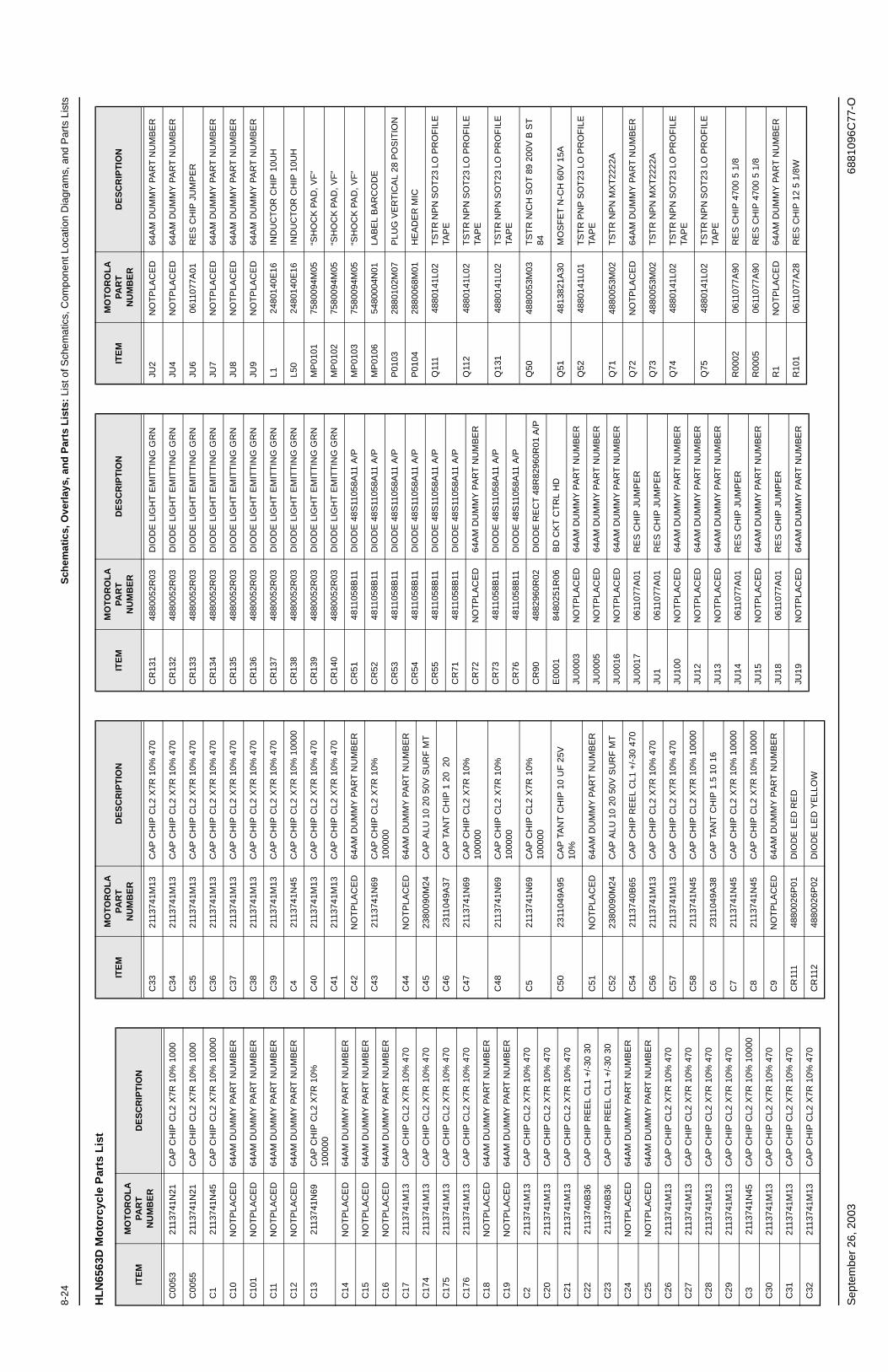
8-24
Sch
emat
ics,
Ove
rlay
s, a
nd
Par
ts L
ists
: Li
st o
f Sch
emat
ics,
Com
pone
nt L
ocat
ion
Dia
gram
s, a
nd P
arts
Lis
ts
Sep
tem
ber
26, 2
003
6881
096C
77-O
HL
N65
63D
Mo
torc
ycle
Par
ts L
ist
ITE
MM
OT
OR
OL
A
PA
RT
N
UM
BE
RD
ES
CR
IPT
ION
C00
5321
1374
1N21
CA
P C
HIP
CL2
X7R
10%
100
0
C00
5521
1374
1N21
CA
P C
HIP
CL2
X7R
10%
100
0
C1
2113
741N
45C
AP
CH
IP C
L2 X
7R 1
0% 1
0000
C10
NO
TP
LAC
ED
64A
M D
UM
MY
PA
RT
NU
MB
ER
C10
1N
OT
PLA
CE
D64
AM
DU
MM
Y P
AR
T N
UM
BE
R
C11
NO
TP
LAC
ED
64A
M D
UM
MY
PA
RT
NU
MB
ER
C12
NO
TP
LAC
ED
64A
M D
UM
MY
PA
RT
NU
MB
ER
C13
2113
741N
69C
AP
CH
IP C
L2 X
7R 1
0%
1000
00
C14
NO
TP
LAC
ED
64A
M D
UM
MY
PA
RT
NU
MB
ER
C15
NO
TP
LAC
ED
64A
M D
UM
MY
PA
RT
NU
MB
ER
C16
NO
TP
LAC
ED
64A
M D
UM
MY
PA
RT
NU
MB
ER
C17
2113
741M
13C
AP
CH
IP C
L2 X
7R 1
0% 4
70
C17
421
1374
1M13
CA
P C
HIP
CL2
X7R
10%
470
C17
521
1374
1M13
CA
P C
HIP
CL2
X7R
10%
470
C17
621
1374
1M13
CA
P C
HIP
CL2
X7R
10%
470
C18
NO
TP
LAC
ED
64A
M D
UM
MY
PA
RT
NU
MB
ER
C19
NO
TP
LAC
ED
64A
M D
UM
MY
PA
RT
NU
MB
ER
C2
2113
741M
13C
AP
CH
IP C
L2 X
7R 1
0% 4
70
C20
2113
741M
13C
AP
CH
IP C
L2 X
7R 1
0% 4
70
C21
2113
741M
13C
AP
CH
IP C
L2 X
7R 1
0% 4
70
C22
2113
740B
36C
AP
CH
IP R
EE
L C
L1 +
/-30
30
C23
2113
740B
36C
AP
CH
IP R
EE
L C
L1 +
/-30
30
C24
NO
TP
LAC
ED
64A
M D
UM
MY
PA
RT
NU
MB
ER
C25
NO
TP
LAC
ED
64A
M D
UM
MY
PA
RT
NU
MB
ER
C26
2113
741M
13C
AP
CH
IP C
L2 X
7R 1
0% 4
70
C27
2113
741M
13C
AP
CH
IP C
L2 X
7R 1
0% 4
70
C28
2113
741M
13C
AP
CH
IP C
L2 X
7R 1
0% 4
70
C29
2113
741M
13C
AP
CH
IP C
L2 X
7R 1
0% 4
70
C3
2113
741N
45C
AP
CH
IP C
L2 X
7R 1
0% 1
0000
C30
2113
741M
13C
AP
CH
IP C
L2 X
7R 1
0% 4
70
C31
2113
741M
13C
AP
CH
IP C
L2 X
7R 1
0% 4
70
C32
2113
741M
13C
AP
CH
IP C
L2 X
7R 1
0% 4
70
C33
2113
741M
13C
AP
CH
IP C
L2 X
7R 1
0% 4
70
C34
2113
741M
13C
AP
CH
IP C
L2 X
7R 1
0% 4
70
C35
2113
741M
13C
AP
CH
IP C
L2 X
7R 1
0% 4
70
C36
2113
741M
13C
AP
CH
IP C
L2 X
7R 1
0% 4
70
C37
2113
741M
13C
AP
CH
IP C
L2 X
7R 1
0% 4
70
C38
2113
741M
13C
AP
CH
IP C
L2 X
7R 1
0% 4
70
C39
2113
741M
13C
AP
CH
IP C
L2 X
7R 1
0% 4
70
C4
2113
741N
45C
AP
CH
IP C
L2 X
7R 1
0% 1
0000
C40
2113
741M
13C
AP
CH
IP C
L2 X
7R 1
0% 4
70
C41
2113
741M
13C
AP
CH
IP C
L2 X
7R 1
0% 4
70
C42
NO
TP
LAC
ED
64A
M D
UM
MY
PA
RT
NU
MB
ER
C43
2113
741N
69C
AP
CH
IP C
L2 X
7R 1
0%
1000
00
C44
NO
TP
LAC
ED
64A
M D
UM
MY
PA
RT
NU
MB
ER
C45
2380
090M
24C
AP
ALU
10
20 5
0V S
UR
F M
T
C46
2311
049A
37C
AP
TA
NT
CH
IP 1
20
20
C47
2113
741N
69C
AP
CH
IP C
L2 X
7R 1
0%
1000
00
C48
2113
741N
69C
AP
CH
IP C
L2 X
7R 1
0%
1000
00
C5
2113
741N
69C
AP
CH
IP C
L2 X
7R 1
0%
1000
00
C50
2311
049A
95C
AP
TA
NT
CH
IP 1
0 U
F 2
5V
10%
C51
NO
TP
LAC
ED
64A
M D
UM
MY
PA
RT
NU
MB
ER
C52
2380
090M
24C
AP
ALU
10
20 5
0V S
UR
F M
T
C54
2113
740B
65C
AP
CH
IP R
EE
L C
L1 +
/-30
470
C56
2113
741M
13C
AP
CH
IP C
L2 X
7R 1
0% 4
70
C57
2113
741M
13C
AP
CH
IP C
L2 X
7R 1
0% 4
70
C58
2113
741N
45C
AP
CH
IP C
L2 X
7R 1
0% 1
0000
C6
2311
049A
38C
AP
TA
NT
CH
IP 1
.5 1
0 16
C7
2113
741N
45C
AP
CH
IP C
L2 X
7R 1
0% 1
0000
C8
2113
741N
45C
AP
CH
IP C
L2 X
7R 1
0% 1
0000
C9
NO
TP
LAC
ED
64A
M D
UM
MY
PA
RT
NU
MB
ER
CR
111
4880
026P
01D
IOD
E L
ED
RE
D
CR
112
4880
026P
02D
IOD
E L
ED
YE
LLO
W
ITE
MM
OTO
RO
LA
P
AR
T
NU
MB
ER
DE
SC
RIP
TIO
N
CR
131
4880
052R
03D
IOD
E L
IGH
T E
MIT
TIN
G G
RN
CR
132
4880
052R
03D
IOD
E L
IGH
T E
MIT
TIN
G G
RN
CR
133
4880
052R
03D
IOD
E L
IGH
T E
MIT
TIN
G G
RN
CR
134
4880
052R
03D
IOD
E L
IGH
T E
MIT
TIN
G G
RN
CR
135
4880
052R
03D
IOD
E L
IGH
T E
MIT
TIN
G G
RN
CR
136
4880
052R
03D
IOD
E L
IGH
T E
MIT
TIN
G G
RN
CR
137
4880
052R
03D
IOD
E L
IGH
T E
MIT
TIN
G G
RN
CR
138
4880
052R
03D
IOD
E L
IGH
T E
MIT
TIN
G G
RN
CR
139
4880
052R
03D
IOD
E L
IGH
T E
MIT
TIN
G G
RN
CR
140
4880
052R
03D
IOD
E L
IGH
T E
MIT
TIN
G G
RN
CR
5148
1105
8B11
DIO
DE
48S
1105
8A11
A/P
CR
5248
1105
8B11
DIO
DE
48S
1105
8A11
A/P
CR
5348
1105
8B11
DIO
DE
48S
1105
8A11
A/P
CR
5448
1105
8B11
DIO
DE
48S
1105
8A11
A/P
CR
5548
1105
8B11
DIO
DE
48S
1105
8A11
A/P
CR
7148
1105
8B11
DIO
DE
48S
1105
8A11
A/P
CR
72N
OT
PLA
CE
D64
AM
DU
MM
Y P
AR
T N
UM
BE
R
CR
7348
1105
8B11
DIO
DE
48S
1105
8A11
A/P
CR
7648
1105
8B11
DIO
DE
48S
1105
8A11
A/P
CR
9048
8296
0R02
DIO
DE
RE
CT
48R
8296
0R01
A/P
E00
0184
8025
1R06
BD
CK
T C
TR
L H
D
JU00
03N
OT
PLA
CE
D64
AM
DU
MM
Y P
AR
T N
UM
BE
R
JU00
05N
OT
PLA
CE
D64
AM
DU
MM
Y P
AR
T N
UM
BE
R
JU00
16N
OT
PLA
CE
D64
AM
DU
MM
Y P
AR
T N
UM
BE
R
JU00
1706
1107
7A01
RE
S C
HIP
JU
MP
ER
JU1
0611
077A
01R
ES
CH
IP J
UM
PE
R
JU10
0N
OT
PLA
CE
D64
AM
DU
MM
Y P
AR
T N
UM
BE
R
JU12
NO
TP
LAC
ED
64A
M D
UM
MY
PA
RT
NU
MB
ER
JU13
NO
TP
LAC
ED
64A
M D
UM
MY
PA
RT
NU
MB
ER
JU14
0611
077A
01R
ES
CH
IP J
UM
PE
R
JU15
NO
TP
LAC
ED
64A
M D
UM
MY
PA
RT
NU
MB
ER
JU18
0611
077A
01R
ES
CH
IP J
UM
PE
R
JU19
NO
TP
LAC
ED
64A
M D
UM
MY
PA
RT
NU
MB
ER
ITE
MM
OTO
RO
LA
PA
RT
N
UM
BE
RD
ES
CR
IPT
ION
JU2
NO
TP
LAC
ED
64A
M D
UM
MY
PA
RT
NU
MB
ER
JU4
NO
TP
LAC
ED
64A
M D
UM
MY
PA
RT
NU
MB
ER
JU6
0611
077A
01R
ES
CH
IP J
UM
PE
R
JU7
NO
TP
LAC
ED
64A
M D
UM
MY
PA
RT
NU
MB
ER
JU8
NO
TP
LAC
ED
64A
M D
UM
MY
PA
RT
NU
MB
ER
JU9
NO
TP
LAC
ED
64A
M D
UM
MY
PA
RT
NU
MB
ER
L124
8014
0E16
IND
UC
TO
R C
HIP
10U
H
L50
2480
140E
16IN
DU
CT
OR
CH
IP 1
0UH
MP
0101
7580
094M
05“S
HO
CK
PA
D, V
F”
MP
0102
7580
094M
05“S
HO
CK
PA
D, V
F”
MP
0103
7580
094M
05“S
HO
CK
PA
D, V
F”
MP
0106
5480
004N
01LA
BE
L B
AR
CO
DE
P01
0328
8010
2M07
PLU
G V
ER
TIC
AL
28 P
OS
ITIO
N
P01
0428
8006
8M01
HE
AD
ER
MIC
Q11
148
8014
1L02
TS
TR
NP
N S
OT
23 L
O P
RO
FIL
E
TAP
E
Q11
248
8014
1L02
TS
TR
NP
N S
OT
23 L
O P
RO
FIL
E
TAP
E
Q13
148
8014
1L02
TS
TR
NP
N S
OT
23 L
O P
RO
FIL
E
TAP
E
Q50
4880
053M
03T
ST
R N
/CH
SO
T 8
9 20
0V B
ST
84
Q51
4813
821A
30M
OS
FE
T N
-CH
60V
15A
Q52
4880
141L
01T
ST
R P
NP
SO
T23
LO
PR
OF
ILE
TA
PE
Q71
4880
053M
02T
ST
R N
PN
MX
T22
22A
Q72
NO
TP
LAC
ED
64A
M D
UM
MY
PA
RT
NU
MB
ER
Q73
4880
053M
02T
ST
R N
PN
MX
T22
22A
Q74
4880
141L
02T
ST
R N
PN
SO
T23
LO
PR
OF
ILE
TA
PE
Q75
4880
141L
02T
ST
R N
PN
SO
T23
LO
PR
OF
ILE
TA
PE
R00
0206
1107
7A90
RE
S C
HIP
470
0 5
1/8
R00
0506
1107
7A90
RE
S C
HIP
470
0 5
1/8
R1
NO
TP
LAC
ED
64A
M D
UM
MY
PA
RT
NU
MB
ER
R10
106
1107
7A28
RE
S C
HIP
12
5 1/
8W
ITE
MM
OT
OR
OL
A
PAR
T
NU
MB
ER
DE
SC
RIP
TIO
N
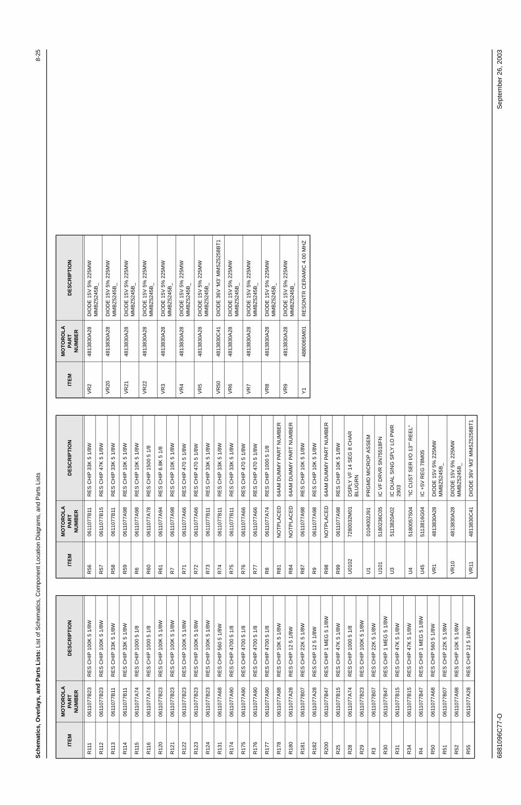
Sch
emat
ics,
Ove
rlay
s, a
nd
Par
ts L
ists
: Li
st o
f Sch
emat
ics,
Com
pone
nt L
ocat
ion
Dia
gram
s, a
nd P
arts
Lis
ts8-
25
6881
096C
77-O
Sep
tem
ber
26, 2
003
R11
106
1107
7B23
RE
S C
HIP
100
K 5
1/8
W
R11
206
1107
7B23
RE
S C
HIP
100
K 5
1/8
W
R11
306
1107
7B11
RE
S C
HIP
33K
5 1
/8W
R11
406
1107
7B11
RE
S C
HIP
33K
5 1
/8W
R11
506
1107
7A74
RE
S C
HIP
100
0 5
1/8
R11
606
1107
7A74
RE
S C
HIP
100
0 5
1/8
R12
006
1107
7B23
RE
S C
HIP
100
K 5
1/8
W
R12
106
1107
7B23
RE
S C
HIP
100
K 5
1/8
W
R12
206
1107
7B23
RE
S C
HIP
100
K 5
1/8
W
R12
306
1107
7B23
RE
S C
HIP
100
K 5
1/8
W
R12
406
1107
7B23
RE
S C
HIP
100
K 5
1/8
W
R13
106
1107
7A68
RE
S C
HIP
560
5 1
/8W
R17
406
1107
7A90
RE
S C
HIP
470
0 5
1/8
R17
506
1107
7A90
RE
S C
HIP
470
0 5
1/8
R17
606
1107
7A90
RE
S C
HIP
470
0 5
1/8
R17
706
1107
7A90
RE
S C
HIP
470
0 5
1/8
R17
806
1107
7A98
RE
S C
HIP
10K
5 1
/8W
R18
006
1107
7A28
RE
S C
HIP
12
5 1/
8W
R18
106
1107
7B07
RE
S C
HIP
22K
5 1
/8W
R18
206
1107
7A28
RE
S C
HIP
12
5 1/
8W
R20
006
1107
7B47
RE
S C
HIP
1 M
EG
5 1
/8W
R25
0611
077B
15R
ES
CH
IP 4
7K 5
1/8
W
R28
0611
077A
74R
ES
CH
IP 1
000
5 1/
8
R29
0611
077B
23R
ES
CH
IP 1
00K
5 1
/8W
R3
0611
077B
07R
ES
CH
IP 2
2K 5
1/8
W
R30
0611
077B
47R
ES
CH
IP 1
ME
G 5
1/8
W
R31
0611
077B
15R
ES
CH
IP 4
7K 5
1/8
W
R34
0611
077B
15R
ES
CH
IP 4
7K 5
1/8
W
R4
0611
077B
47R
ES
CH
IP 1
ME
G 5
1/8
W
R50
0611
077A
68R
ES
CH
IP 5
60 5
1/8
W
R51
0611
077B
07R
ES
CH
IP 2
2K 5
1/8
W
R52
0611
077A
98R
ES
CH
IP 1
0K 5
1/8
W
R55
0611
077A
28R
ES
CH
IP 1
2 5
1/8W
ITE
MM
OTO
RO
LA
PA
RT
N
UM
BE
RD
ES
CR
IPT
ION
R56
0611
077B
11R
ES
CH
IP 3
3K 5
1/8
W
R57
0611
077B
15R
ES
CH
IP 4
7K 5
1/8
W
R58
0611
077B
11R
ES
CH
IP 3
3K 5
1/8
W
R59
0611
077A
98R
ES
CH
IP 1
0K 5
1/8
W
R6
0611
077A
98R
ES
CH
IP 1
0K 5
1/8
W
R60
0611
077A
78R
ES
CH
IP 1
500
5 1/
8
R61
0611
077A
94R
ES
CH
IP 6
.8K
5 1
/8
R7
0611
077A
98R
ES
CH
IP 1
0K 5
1/8
W
R71
0611
077A
66R
ES
CH
IP 4
70 5
1/8
W
R72
0611
077A
66R
ES
CH
IP 4
70 5
1/8
W
R73
0611
077B
11R
ES
CH
IP 3
3K 5
1/8
W
R74
0611
077B
11R
ES
CH
IP 3
3K 5
1/8
W
R75
0611
077B
11R
ES
CH
IP 3
3K 5
1/8
W
R76
0611
077A
66R
ES
CH
IP 4
70 5
1/8
W
R77
0611
077A
66R
ES
CH
IP 4
70 5
1/8
W
R8
0611
077A
74R
ES
CH
IP 1
000
5 1/
8
R81
NO
TP
LAC
ED
64A
M D
UM
MY
PA
RT
NU
MB
ER
R84
NO
TP
LAC
ED
64A
M D
UM
MY
PA
RT
NU
MB
ER
R87
0611
077A
98R
ES
CH
IP 1
0K 5
1/8
W
R9
0611
077A
98R
ES
CH
IP 1
0K 5
1/8
W
R98
NO
TP
LAC
ED
64A
M D
UM
MY
PA
RT
NU
MB
ER
R99
0611
077A
98R
ES
CH
IP 1
0K 5
1/8
W
U01
0272
8003
2M01
DS
PLY
VF
14
SE
G 8
CH
AR
B
LUG
RN
U1
0104
002J
91P
RG
MD
MIC
RO
P A
SS
EM
U10
151
8023
6C05
IC V
F D
RV
R S
N75
518F
N
U3
5113
820A
02IC
DU
AL
SIN
G S
PLY
LO
PW
R
2903
U4
5180
057S
04“I
C C
US
T S
ER
I/O
13”
” R
EE
L”
U45
5113
816G
04IC
+5V
RE
G 7
8M05
VR
148
1383
0A28
DIO
DE
15V
5%
225
MW
M
MB
Z52
45B
_
VR
1048
1383
0A28
DIO
DE
15V
5%
225
MW
M
MB
Z52
45B
_
VR
1148
1383
0C41
DIO
DE
36V
‘M3’
MM
SZ
5258
BT
1
ITE
MM
OT
OR
OL
A
PAR
T
NU
MB
ER
DE
SC
RIP
TIO
N
VR
248
1383
0A28
DIO
DE
15V
5%
225
MW
M
MB
Z52
45B
_
VR
2048
1383
0A28
DIO
DE
15V
5%
225
MW
M
MB
Z52
45B
_
VR
2148
1383
0A28
DIO
DE
15V
5%
225
MW
M
MB
Z52
45B
_
VR
2248
1383
0A28
DIO
DE
15V
5%
225
MW
M
MB
Z52
45B
_
VR
348
1383
0A28
DIO
DE
15V
5%
225
MW
M
MB
Z52
45B
_
VR
448
1383
0A28
DIO
DE
15V
5%
225
MW
M
MB
Z52
45B
_
VR
548
1383
0A28
DIO
DE
15V
5%
225
MW
M
MB
Z52
45B
_
VR
5048
1383
0C41
DIO
DE
36V
‘M3’
MM
SZ
5258
BT
1
VR
648
1383
0A28
DIO
DE
15V
5%
225
MW
M
MB
Z52
45B
_
VR
748
1383
0A28
DIO
DE
15V
5%
225
MW
M
MB
Z52
45B
_
VR
848
1383
0A28
DIO
DE
15V
5%
225
MW
M
MB
Z52
45B
_
VR
948
1383
0A28
DIO
DE
15V
5%
225
MW
M
MB
Z52
45B
_
Y1
4880
065M
01R
ES
ON
TR
CE
RA
MIC
4.0
0 M
HZ
ITE
MM
OT
OR
OL
A
PA
RT
N
UM
BE
RD
ES
CR
IPT
ION

8-26
Sch
emat
ics,
Ove
rlay
s, a
nd
Par
ts L
ists
: Li
st o
f Sch
emat
ics,
Com
pone
nt L
ocat
ion
Dia
gram
s, a
nd P
arts
Lis
ts
Sep
tem
ber
26, 2
003
6881
096C
77-O
Fig
ure
8-14
. HC
N10
78J
(Sta
ndar
d), H
CN
1121
D (
Rea
r) W
9 C
ontr
ol H
ead
Sch
emat
ic (
Sid
e 1
of 2
)
KR4
BUSY
BUS-
CO
NN
ECTO
R
BUS+
FIL_2
OR
DAM
AGE
TO T
HE
SPEA
KER
-LO
BATT
-
KR1
DAT
A(7:
0)
3.)
ASTE
RIS
K (*
) IN
DIC
ATES
PAR
TS N
OT
NO
RM
ALLY
PLA
CED
IN S
TAN
DAR
D C
ON
FIG
UR
ATIO
N
J101
KS1
KR3
HEA
D
VIP-
OU
T-1
VF-CONTROL
GROUND
VIP-
IN-1
SPAR
E-1
DO
NO
T PR
OBE
U3
PIN
SPARE-2
SHO
RT
TO G
RO
UN
D T
O
NC MIC
-HU
B
VIP-
OU
T-2
SPAR
E-2
NO
TE: Q
40 U
SED
FO
R P
OSI
TIVE
GR
OU
ND
IGN
ITIO
N S
ERVI
CE
5 VO
LT
1.)
ALL
RES
ISTA
NC
E IS
IN O
HM
S. A
LL C
APAC
ITAN
CE
IN P
ICO
-FAR
ADS
UN
LESS
NO
TED
OTH
ERW
ISE.
DATA(7:0)
DAT
A(7:
0)
DIS
ABLE
WAT
CH
-DO
G T
IMER
CLOCK
NC
ADD
RES
S (8
:12)
DAT
A(7:
0)
EMER
GEN
CY
DATA
KS3KS2
DEK
-CLO
CK
DEK
-DAT
A-O
UT
VIP-
OU
T-3
VIP-
OU
T-1
STROBE
(GR
EEN
)
MIC
-PTT
A+
REG
ISTE
R
FLEX
CAB
LE
2.)
PAR
T U
SAG
E M
AY V
ARY
WIT
H A
PPLI
CAT
ION
. R
EFER
TO
PAR
TS L
IST
FOR
USA
GE
INFO
RM
ATIO
N.
SWB+
DIG
ITAL
GR
OU
ND
VIP-
OU
T-2
VIP-
OU
T-3
EEPR
OM
CIR
CU
ITR
Y M
AY O
CC
UR
.
LATC
H
LATCH
ADD
RES
S (7
:0)
+43V
SPEA
KER
-HI
MIC
-SW
B+
SHIF
T
GR
OU
ND
5 W
ITH
PO
WER
APP
LIED
CO
NTR
OL
WAR
NIN
G!
IGN
+
VIP-
IN-3
VIP-
IN-2
MIC
RO
PRO
CES
SOR
PTT/
HU
B-R
EF
KR5
PRO
M
P103
NC
(OR
ANG
E)
KR2
SER
IAL
I/0IG
N-
ADD
RES
S (8
:12)
NO
TES:
KS4KS5
REG
ULA
TOR
RES
ET
FIL_1
MIC
-LO
MIC
-HI
5.1
36
VR6 15
V
R55
1
23
Q74
3
JU3 0
18
Q17
1
10K
R16
1M
C78
M05
U46
2GN
D
1IN
3O
UT
U8
PWR
_GN
D
7GN
D
14 VCC
2
12
10K
R16
3
1KR38
1uF
C16
5
C20
7
4
31 15
470p
F
470p
F
C27
6
C20
647
0pF
+5V_
FIL
4345
SWB+
L2
9.10
7uH
.01u
F
C53
C16
470p
F
1615
R41
10K
A48
A39
A2
Q16
1
A8
3A1
2
30A1
331
+5V_
FIL
32+5
V_FI
L
4A7
5A6
6A5
7
D6
22D
723
CE*
24A1
025
OE*
26G
ND
27A1
128
A929
D1
15D
216
GN
D
17N
C18
D3
19D
4
2+5
V_FI
L
20D
521
U7
SOC
KET
1N
C
10A1
11A0
12G
ND
13D
014
15pF
C22
0JU
19
10K
R84
5
CR
164
3
12
10K
R20
VR11 15
V
C27
7
470p
F
5.1
R53
L1
9.10
7uH
C27
5
41
470p
F
0
7
10K
R01
65
JU5
0
JU16
*
1135
VR2
470p
F
12
15V
10K
C18
C17
347
0pF
+5V
R19
C7
.01u
F
10K
R81
JU21
*
44
0
R27
10K
C12
15V
VR3
Q71
1
2 3
470p
F
10uF
CR
161
31 2
C52
1uF
17N
C1
26N
C2
30N
C3
NC
4122
RD
Y_BU
SY*
32 VCC
16VS
S
C46
19D
420
D5
D6
21 22D
7
23EN
_CE
25EN
_OE
31EN
_WE
NC
1
5A6
4A7
29A8
28A9
13D
014
D1
15D
218
D3
10A1
24A1
027
A11
3A1
2
9A2
8A3
7A4
6A5
9
+5V_
FIL
U5
AT28
HC
64
11A0
A212
A39
A46
A55
A62
A7
20VC
C
D5
4D
63
D7
11EN
_LE
1EN
_OE 10GN
D
19A0
16A1
15
18D
017
D1
14D
213
D3
8D
47
R25
MC
74H
C37
3U
10
47K
100K
R5
15V
10
10K
R13
VR5
SWB+
5
JU20 0
R16
+5V
13
10K
470p
F
C73
49
47K
R99
SWB+
470p
F
T60
77J0
3
1 2 3
4 5 6
C39
10K
10K
R74
6
SWB+
R59
R18
10K
Q16
2
10K
470p
F
C75
R15
+5V
C54
470p
F
+5V
12
7.94
88M
Hz
21
26
C45
Y1 7160
C27
4
10uF
+5V_
FIL
+5V_
FIL
470p
F
48
22K
R6
C28 47
0pF
30
+5V
9
470p
F
C27
2
10K
R18
3
43V
C17
0
0.1u
F
L23
VR50
470p
F
22uH
1 2 3 4 5 6 7
C72
470p
F
C26
0
CR
74
CR
75
CR
90
JU4* 0
14
R40
1K
32
C63
0.1u
F
15V
VR10
0
JU23
*
10K
R28
4.7K
R8
9.10
7uH
L50
C50
10uF
40
U8B
MC
74H
C00
5 46
1011
R29
10K
R57
33K
.01u
F
C51
U3B
LM29
03
6 57
8 4
R56
6.8K
33K
+5V_
FIL
SWB+
R60
R24
15V
VR8
10K
R44
33K
+5V
654321047
KR
34
470p
F
C14
+5V
7
11
+5V
+5V
8
+5V
47
0
JU12
*
SWB+
470p
F
13 1211
C41
Q17
0
+5V
MC
74H
C00
U8C
R87
14
10K
470p
F
+5V
20
33K
C20
2
3
A+_I
GN
R00
58
470p
F
C20
R50
470p
F
C17
4
R98
470
C29
10K
470p
F47
0pF
+5V
C30
R17
34.
7K
22K
R18
1
15V
VR1
JU11
*
0
5
CR
72
C27
1
470p
F
0.1u
FC
61
C17
1
470p
F
R31
24
47K
50
C64
0.1u
F
Q23
132
+5V
+5V
SWB+
R71
33K
2 31
8 4C
176
470p
F
U3A
LM29
03
470p
F
C38
C66
0.1u
F
19
R75
10K
5.1
R54
33
+5V
+5V
1318
2
12
1KR
39
2
+5V
1KR35
2119
470p
F
C19
C6
470p
FC
21
SWB+
1.5u
F
0
JU17
*
28
33K
R72
+5V_
FIL
37
PTH
-1
3+5
VSW
B+
PTH
-3
CR
162
31 2
C13
+5V
R14
470p
F47
0pF
10K
C27
3
470p
F
C44
R16
6
2.2K
1MEG
A+_I
GN
Q72
1
2 3
R20
0
C65
0.1u
F
22K
R51
C67
0.1u
F
2.2K
10K
R16
4
0
R17
2
C62
0.1u
F
Q73
1
2 3
1KR61
Q50
S(3)
G(2
)
D(1
)
38
C56
10
1 23
.01u
F
C1
.01u
F
MC
74H
C00
U8D
33K
R73
0
0 1 2 3 4 5 6 7
470p
F
JU2*
15V
SWB+
C47
+5V
VR9
470p
F
C57
1KR37
8
+5V
20 7
R12
171K
46
R17
1
47K
R17
0
100K
MC
74H
C00
9 108
27
U8A
470p
F
C24
6
CR
71
0
470p
F
C15
JU24
*
SWB+
34
PTH
-2
1615
VVR
7
33K
R22
8
4
0
JU9*
1VSS
18XI
RQ
8 XTAL
0
JU10
*
KR4
KR5
50
RES
ET*
17
STRA_AS4
STR
B_R
_W*
6
26 VDD52 VRH51 VRL
PD4_
SCK
25PD
5_SS
*
43PE
0_AN
045
VIP_
IN_1
VIP_
IN_2
47 49KR
144
KR2
46KR
348
PC4_
A4_D
4
PC5_A5_D5 1415PC6_A6_D6
PC7_A7_D7 16
20RX_DATA21TX_DATA22PD2_MISO
PD3_
MO
SI2324
PB4_A1237PB5_A1336PB6_A1435PB7_A15
9PC
0_A0
_D0
10PC
1_A1
_D1
11PC
2_A2
_D2
12PC
3_A3
_D3
13
STROBELATCH29
28 BUSY_OUT*27 DEK_DATA-OUT
42PB0_A841PB1_A940PB2_A1039PB3_A1138
EXTAL
19IR
Q
3M
OD
A_LI
R*
2M
OD
B_VS
TBY
34 PTT33 VIP_IN_332 BUSY_IN*31 DEK_CLOCK30
MC
68H
C11
A1
U2
5C
LK_E
7
0
470p
FC
40
C74
7654321
R17
1
470p
F
R30
10K
CR
55
10K
+5V
47K
R43
78
9
VR4
15V
7 6 5 4 3 2 1 0
CR
51
47K
R18
2
R21
11
Q75
C23
1MEG
29
4.7p
F
SWB+
470p
F
C76
JU22
*0
VR12
15V
11
12pF
C24
5
R52
JU13
*0
17
10
10K
8
470p
FC
279
3 4 5 6 7
C27
8
470p
F
R1
10K
0 1 2
CR
73
10K
R23
0JU
18
9
C27 47
0pF
C17
R7
4.7K
SWB+
470p
F
226
4
C71
470p
F
470p
FC
37
C17
5
470p
F
1
JU1 0
Q40
OFF1 ON
3
CR
76
S1SW
ITC
H
G1
4
G2
52IN
VR51
415
V
12
12Q
711
Q8
9D
ATA
10Q
S*
2SE
R_D
AT_I
N
1LA
TCH
VDD16
15EN
_OE
8G
ND
4Q
15
Q2
Q3
6 7Q
414
Q5
Q6
13
MC
1409
BU
6
3C
LK
1KR33
10
SWB+
10K
R26
22 35VI
P_IN
_324
VIP_
IN_1
*
21VI
P_IN
_2*
36VI
P_IN
_3*
44W
DT_
IN_T
_CAP
2W
DT_
TIC
KLE
43W
DT_
T_C
AP
37
9R
ESET
4R
ESET
*
7R
ESET
_FIL
TR
31R
ES_H
UB
RX_
DAT
A20 19
TX_D
ATA
25VI
P_IN
_1VI
P_IN
_2
15
12N
C7
18N
C8
23N
C9
42O
SC_O
UT
6
POS5V3
POS5_REG
38PT
T
PTT*
28
29IG
N*
14N
C8
NC
140
NC
2N
C3
27 26N
C4
33N
C5
NC
6
16 17BU
S+
41EX
T_O
SC_I
N
1GND5GND
34GND
30H
UB_
INV
32H
UB_
POL
IGN
SC74
487F
U4
39
APOS
BUSY
1011
BUSY
_IN
*
13BU
SY_O
UT*
BUS-
CR
163
3
12
R10 220
R32
21
DAT
A(7:
0)
47K
ADDRESS(8:12)
ADD
RES
S(7:
0)

Sch
emat
ics,
Ove
rlay
s, a
nd
Par
ts L
ists
: Li
st o
f Sch
emat
ics,
Com
pone
nt L
ocat
ion
Dia
gram
s, a
nd P
arts
Lis
ts8-
27
6881
096C
77-O
Sep
tem
ber
26, 2
003
Fig
ure
8-15
. HC
N10
78J
(Sta
ndar
d), H
CN
1121
D (
Rea
r) W
9 C
ontr
ol H
ead
Sch
emat
ic (
Sid
e 2
of 2
)
(RE
D)
XM
IT(Y
EL)
BU
SY
VF
_CO
NT
RO
L
GR
ID
AN
OD
E
1
P10
1
34
5
OP
T4
MU
SE
L
KS
3
KR
5
+5V
9
AN
OD
E
AN
OD
E
AN
OD
E
IS IN
PIC
OFA
RA
DS
UN
LES
S N
OT
ED
OT
HE
RW
ISE
.
2.)
AS
TE
RIS
K (
*) D
EN
OT
ES
UN
-US
ED
PA
RT
PE
R T
HIS
1.)
ALL
RE
SIS
TAN
CE
IS IN
OH
MS
. CA
PAC
ITA
NC
E
SPA
RE
_2
KS
5
KS
4
KS
1
GR
ID
GR
ID
AN
OD
E
AN
OD
E
AN
OD
E
KR
3
KR
4
CLO
CK
VU
HO
ME
0
SW
B+
DAT
A_I
N
AN
OD
E
AN
OD
E
AN
OD
E
AP
PLI
CAT
ION
.
GR
ID
AN
OD
E
VF
DR
IVE
R
GR
ID
GR
ID
GR
ID
NO
TE
S:
GR
ID
GN
D
LAT
CH
ST
RO
BE
+43
V
FIL
AM
EN
T 1
FIL
AM
EN
T 2
STA
RP
ND
OP
T6
2
KR
1
KS
2
KR
2
67
OP
T3
MD
DIM
8
OP
T5
OP
T2
VD
OP
T1
VF
DIS
PLA
Y
FLE
X C
AB
LE
AN
OD
E
AN
OD
E
AN
OD
E
GR
ID
GR
ID
GR
ID
CR
134
22 194 6
SW
B+
SW
B+
20
100K
Q13
4
CR
112
R11
2Q
111
1.5K
R15
0
5
10K
C55
0.1u
F
R13
2
S11
1
12
27
SW
B+ R
137
SW
B+
CR
113
10K
R14
2
Q11
5
16
CR
111
17
SW
B+
SW
B+
SW
B+
100K
R12
4
Q13
3
Q13
1
R11
61K
470p
FC
139
S10
5
12
2
S10
1
12
1.5K
S10
2
1
10K
R15
4
R14
4
Q11
7
12
S11
0
12
CR
116
10
S12
6
CR
120
11
1 2
1
2
S12
3S
127
12
S13
1
CR
118
220
R15
8
R13
822
022
0
+5V
S12
4
12
R13
1
9
SW
B+
1.5K
100K
RT
133
R11
5
+5V
R13
4
SW
B+ 1K
33K
33K
R11
3R11
1
R11
4
R14
110
K
100K
Q11
4
R15
5
10K
R14
5
1.5K
Q11
8Q
119
8 714
Q9
34
SE
RIA
L_O
UT
2
24LA
TC
H
+5V
44
+43V
1
15
Q30
5
Q31
4
Q32
3
Q4
39
Q5
38
Q6
37
Q7
36
Q8
35
Q23
13
Q24
12
Q25
11
Q26
10
Q27
9
Q28
8
Q29
7
Q3
40
Q16
25
Q17
20
Q18
19
Q19
17
Q2
41
Q20
16
Q21
15
Q22
14
NC
429
Q1
42
Q10
33
Q11
32
Q12
31
Q13
30
Q14
27
Q15
26
U10
1
ST
RO
BE
21C
LK23
DAT
A_I
N43
GN
D 22
NC
16
NC
218
NC
328
S10
9
12
UC
Q58
18E
PF
100K
R12
110
0KR
120
12
S12
5
12
12
S12
2S
136
12
S13
4
12
S10
0
12
S10
4
12
S10
3
R13
6
2.2K
C14
147
0pF
S10
6
12
JU8
0
0JU7
+5V
R14
8*0
C13
5
470p
F
SW
B+
+5V
2118 12
3K
25L
18M
9N
27N
C
13
15G
514
G6
13G
712
G8
10G
9
21H
26I
11J
28F
ILA
ME
NT
2
5G
23G
1
6G
10
7G
11
22G
219
G3
17G
4
U10
2
2A
4B
20C
16D
8E
24F
1F
ILA
ME
NT
1
12
PR
-483
-05
S12
1
1
2
S13
3
CR
137
SW
B+
CR
135
CR
136
Q13
3
CR
140
CR
131
CR
138
S10
8
12
S10
7
12
1.5K
R15
7
SW
B+
10K
R14
7
Q12
0
1.5K
R15
6
R14
6
CR
119
CR
114
10K
R15
11.
5K
12
Q13
2
SW
B+
S13
5
Q11
2
Q13
0
10K
R12
9
R13
0
R12
310
0K
4.7K
100K
R12
2
R15
31.
5K
R14
310
K
CR
132
SW
B+
R13
56.
8K
CR
133
CR
117
33K
220
R15
9
Q11
0R
149
2.2K
R13
9
+5V
S13
2
12
2 3
C13
4
1
C13
3
470p
F
470p
F
C13
2
470p
F
470p
F
C13
1
10K
R14
0
Q11
3
CR
115
Q11
6
R15
21.
5K

8-28
Sch
emat
ics,
Ove
rlay
s, a
nd
Par
ts L
ists
: Li
st o
f Sch
emat
ics,
Com
pone
nt L
ocat
ion
Dia
gram
s, a
nd P
arts
Lis
ts
Sep
tem
ber
26, 2
003
6881
096C
77-O
Fig
ure
8-16
. HC
N10
78J
(Sta
ndar
d), H
CN
1121
D (
Rea
r) W
9 C
ontr
ol H
ead
Com
pone
nt L
ocat
ion
Dia
gram
(V
iew
ed fr
om S
ide
1)
U5
U10
U2
Y1
U7
U8
L23
L1
U4
C45
U46
P103
Q73
S1
Q72
C50
Q71
U3
T60
C52
Q50
S123
U10
2
U10
1
S121
S122
S124
S133
S134
S135
S131
S136
S108
S107
S110
S100
S111
S109
S127
S102
S106
S105
S104
S103
S101
S126
S125
U6
VR51
C47
C20
C19 C16
C12 C21
C74C17
C18C15C13
C44
R20
C14
R19
R16 L2
R37
C27
6
C64
L50
C56
C27
8
R54
CR
51Q
170
R17
2
C17
0R
163
CR
161
CR
162
CR
111
CR
112
CR
136
CR
137
CR
135
CR
113
CR
115
CR
117
CR
119
CR
118
CR
120
CR
114
CR
116
CR
138
CR
139
CR
140
CR
133
CR
132
CR
131
CR
134
S132
114
1528
CR
163
C165
R12
C29
C30
C39
C40
C41
C28
C75
C26
C27
R38 C38
R173
C207
C206
C6
R200
C27
7
CR90
C275
C46
C274
R72
R71 C271
VR50
RT133
C55
110
87
54
32
1112
1314
1516
1733
2829
3031
3226
2750
4546
4748
4943
4440
4137
3836
3435
2021
1819
2324
K A
B
K
K
AA
6
6
G
DS
5
58
44
1
1
1
1
1
1
1
2
2
2
2
3
3
3
CE
BC
E
BC
E
K
AC
BE
K
A
K
A89
16
7
7
7
8
8
14
1 4
513
1420
21
2133
3446
47
29
301
1
1
1
4
513
142010
11
20
20
2129
30
17
1828
2939
40
6
7
1
17
1828
2939
40
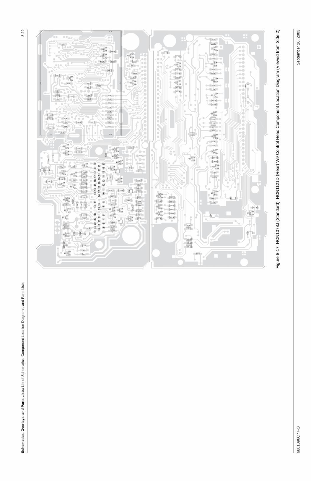
Sch
emat
ics,
Ove
rlay
s, a
nd
Par
ts L
ists
: Li
st o
f Sch
emat
ics,
Com
pone
nt L
ocat
ion
Dia
gram
s, a
nd P
arts
Lis
ts8-
29
6881
096C
77-O
Sep
tem
ber
26, 2
003
Fig
ure
8-17
. HC
N10
78J
(Sta
ndar
d), H
CN
1121
D (
Rea
r) W
9 C
ontr
ol H
ead
Com
pone
nt L
ocat
ion
Dia
gram
(V
iew
ed fr
om S
ide
2)
R29
R28
R27
R26
R75
R30
R41
R40
R39
C66
R21
C24
C23 R23
C62
C63
R33
R35
C61
R14
R44
R13
R99 C1
R43
R22
R25
JU19
JU18
JU23
JU6
JU5
JU1
C202
JU13
JU12
JU22
C67
JU21
JU20
R10 JU17
R60
R1
C71R134
R120
C13
5
R153
C13
9
R131
C13
2
R143
R141
R151
R147
R157
R145
R155
JU7
JU8
R146
R156
R138
R144
R154
R142
R152
R140
R150
R149
R148R115
R113
R111
R116
R114
R112
C141
R158
R159
R124
R121
R122
R123
C133
R135
R136
R137
R130
R139
R129
R132
R56
R58
R57
C54
R61
R51
C51
R52
C53
C57
C17
4
C73
R73
C72
C27
2C
273
CR
72C
R73
C17
6
R87
JU10
JU9
VR8
VR10
VR9
VR4
VR6
Q40
VR1
R31
R84
JU11
JU3
VR3
VR12
CR
76C
175
JU2
JU4
VR7
VR11
C17
3
VR2
CR
75Q
75
Q16
1Q
171
Q16
2
Q23
Q74
CR
74
C7
VR5
R6
R8
C76
R98
CR
164
C27
9
C24
6
R59
CR
71
Q13
2Q
133
Q13
4 Q11
6
Q13
1
Q13
0
Q12
0Q
114
Q11
8Q
119
Q11
7
C13
1C
134
Q11
5Q
113
Q11
0
Q11
1Q
112
R81
R24R34R5
R7
R32
R183 C37
R17
R74
R15
R18
R182
R181
R55
R50
R53
R161
R170
R171
C171
R166
C65
R165R164
C22
C
BE
C
A
AA
KK
K
BE
C
BE
C
BE
C
BE
C
BE
C
BE
C
BE
C
BE
C
BE
C
BE
C
BE
C
BE
C
BE
C
BE
C
BE
C
BE
C
BE
C
BE
C
BE
C
BE
C
BE
C
BE
AA
K
AA
KA
A
K
AA
A
K
KK
AA
K
AA
K
AA
K
AA
K
AA
KA
A
K
AA
K
A
KK
A
KK
A
KK
A
KK
A
KK
110
87
54
32
1112
1314
1516
1733
2829
3031
3226
2750
4546
4748
4943
4440
4137
3836
3435
2021
1819
2324
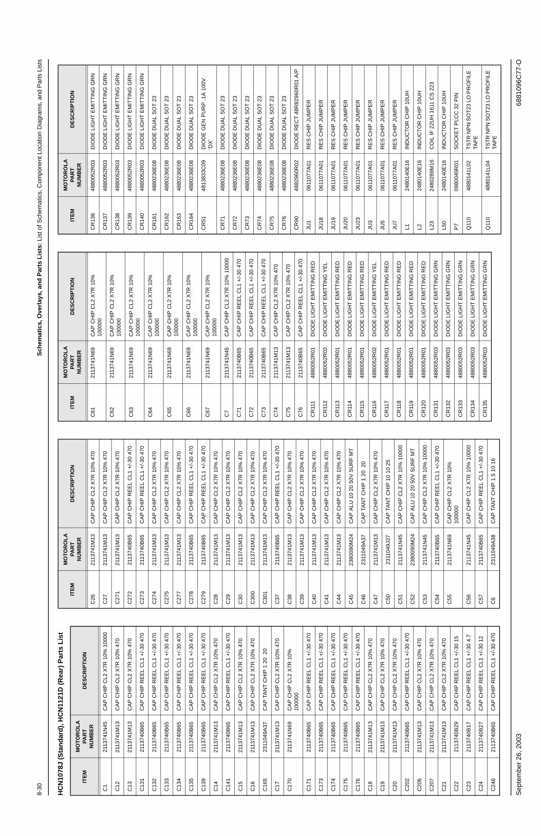
8-30
Sch
emat
ics,
Ove
rlay
s, a
nd
Par
ts L
ists
: Li
st o
f Sch
emat
ics,
Com
pone
nt L
ocat
ion
Dia
gram
s, a
nd P
arts
Lis
ts
Sep
tem
ber
26, 2
003
6881
096C
77-O
HC
N10
78J
(Sta
nd
ard
), H
CN
1121
D (
Rea
r) P
arts
Lis
t
ITE
MM
OT
OR
OL
A
PA
RT
N
UM
BE
RD
ES
CR
IPT
ION
C1
2113
741N
45C
AP
CH
IP C
L2 X
7R 1
0% 1
0000
C12
2113
741M
13C
AP
CH
IP C
L2 X
7R 1
0% 4
70
C13
2113
741M
13C
AP
CH
IP C
L2 X
7R 1
0% 4
70
C13
121
1374
0B65
CA
P C
HIP
RE
EL
CL1
+/-
30 4
70
C13
221
1374
0B65
CA
P C
HIP
RE
EL
CL1
+/-
30 4
70
C13
321
1374
0B65
CA
P C
HIP
RE
EL
CL1
+/-
30 4
70
C13
421
1374
0B65
CA
P C
HIP
RE
EL
CL1
+/-
30 4
70
C13
521
1374
0B65
CA
P C
HIP
RE
EL
CL1
+/-
30 4
70
C13
921
1374
0B65
CA
P C
HIP
RE
EL
CL1
+/-
30 4
70
C14
2113
741M
13C
AP
CH
IP C
L2 X
7R 1
0% 4
70
C14
121
1374
0B65
CA
P C
HIP
RE
EL
CL1
+/-
30 4
70
C15
2113
741M
13C
AP
CH
IP C
L2 X
7R 1
0% 4
70
C16
2113
741M
13C
AP
CH
IP C
L2 X
7R 1
0% 4
70
C16
523
1104
9A37
CA
P T
AN
T C
HIP
1 2
0 2
0
C17
2113
741M
13C
AP
CH
IP C
L2 X
7R 1
0% 4
70
C17
021
1374
1N69
CA
P C
HIP
CL2
X7R
10%
10
0000
C17
121
1374
0B65
CA
P C
HIP
RE
EL
CL1
+/-
30 4
70
C17
321
1374
0B65
CA
P C
HIP
RE
EL
CL1
+/-
30 4
70
C17
421
1374
0B65
CA
P C
HIP
RE
EL
CL1
+/-
30 4
70
C17
521
1374
0B65
CA
P C
HIP
RE
EL
CL1
+/-
30 4
70
C17
621
1374
0B65
CA
P C
HIP
RE
EL
CL1
+/-
30 4
70
C18
2113
741M
13C
AP
CH
IP C
L2 X
7R 1
0% 4
70
C19
2113
741M
13C
AP
CH
IP C
L2 X
7R 1
0% 4
70
C20
2113
741M
13C
AP
CH
IP C
L2 X
7R 1
0% 4
70
C20
221
1374
0B65
CA
P C
HIP
RE
EL
CL1
+/-
30 4
70
C20
621
1374
1M13
CA
P C
HIP
CL2
X7R
10%
470
C20
721
1374
1M13
CA
P C
HIP
CL2
X7R
10%
470
C21
2113
741M
13C
AP
CH
IP C
L2 X
7R 1
0% 4
70
C22
2113
740B
29C
AP
CH
IP R
EE
L C
L1 +
/-30
15
C23
2113
740B
17C
AP
CH
IP R
EE
L C
L1 +
/-30
4.7
C24
2113
740B
27C
AP
CH
IP R
EE
L C
L1 +
/-30
12
C24
621
1374
0B65
CA
P C
HIP
RE
EL
CL1
+/-
30 4
70
C26
2113
741M
13C
AP
CH
IP C
L2 X
7R 1
0% 4
70
C27
2113
741M
13C
AP
CH
IP C
L2 X
7R 1
0% 4
70
C27
121
1374
1M13
CA
P C
HIP
CL2
X7R
10%
470
C27
221
1374
0B65
CA
P C
HIP
RE
EL
CL1
+/-
30 4
70
C27
321
1374
0B65
CA
P C
HIP
RE
EL
CL1
+/-
30 4
70
C27
421
1374
1M13
CA
P C
HIP
CL2
X7R
10%
470
C27
521
1374
1M13
CA
P C
HIP
CL2
X7R
10%
470
C27
721
1374
1M13
CA
P C
HIP
CL2
X7R
10%
470
C27
821
1374
0B65
CA
P C
HIP
RE
EL
CL1
+/-
30 4
70
C27
921
1374
0B65
CA
P C
HIP
RE
EL
CL1
+/-
30 4
70
C28
2113
741M
13C
AP
CH
IP C
L2 X
7R 1
0% 4
70
C29
2113
741M
13C
AP
CH
IP C
L2 X
7R 1
0% 4
70
C30
2113
741M
13C
AP
CH
IP C
L2 X
7R 1
0% 4
70
C30
021
1374
1M13
CA
P C
HIP
CL2
X7R
10%
470
C30
121
1374
1M13
CA
P C
HIP
CL2
X7R
10%
470
C37
2113
740B
65C
AP
CH
IP R
EE
L C
L1 +
/-30
470
C38
2113
741M
13C
AP
CH
IP C
L2 X
7R 1
0% 4
70
C39
2113
741M
13C
AP
CH
IP C
L2 X
7R 1
0% 4
70
C40
2113
741M
13C
AP
CH
IP C
L2 X
7R 1
0% 4
70
C41
2113
741M
13C
AP
CH
IP C
L2 X
7R 1
0% 4
70
C44
2113
741M
13C
AP
CH
IP C
L2 X
7R 1
0% 4
70
C45
2380
090M
24C
AP
ALU
10
20 5
0V S
UR
F M
T
C46
2311
049A
37C
AP
TA
NT
CH
IP 1
20
20
C47
2113
741M
13C
AP
CH
IP C
L2 X
7R 1
0% 4
70
C50
2311
049J
27C
AP
TA
NT
CH
IP 1
0 10
25
C51
2113
741N
45C
AP
CH
IP C
L2 X
7R 1
0% 1
0000
C52
2380
090M
24C
AP
ALU
10
20 5
0V S
UR
F M
T
C53
2113
741N
45C
AP
CH
IP C
L2 X
7R 1
0% 1
0000
C54
2113
740B
65C
AP
CH
IP R
EE
L C
L1 +
/-30
470
C55
2113
741N
69C
AP
CH
IP C
L2 X
7R 1
0%
1000
00
C56
2113
741N
45C
AP
CH
IP C
L2 X
7R 1
0% 1
0000
C57
2113
740B
65C
AP
CH
IP R
EE
L C
L1 +
/-30
470
C6
2311
049A
38C
AP
TA
NT
CH
IP 1
.5 1
0 16
ITE
MM
OTO
RO
LA
P
AR
T
NU
MB
ER
DE
SC
RIP
TIO
N
C61
2113
741N
69C
AP
CH
IP C
L2 X
7R 1
0%
1000
00
C62
2113
741N
69C
AP
CH
IP C
L2 X
7R 1
0%
1000
00
C63
2113
741N
69C
AP
CH
IP C
L2 X
7R 1
0%
1000
00
C64
2113
741N
69C
AP
CH
IP C
L2 X
7R 1
0%
1000
00
C65
2113
741N
69C
AP
CH
IP C
L2 X
7R 1
0%
1000
00
C66
2113
741N
69C
AP
CH
IP C
L2 X
7R 1
0%
1000
00
C67
2113
741N
69C
AP
CH
IP C
L2 X
7R 1
0%
1000
00
C7
2113
741N
45C
AP
CH
IP C
L2 X
7R 1
0% 1
0000
C71
2113
740B
65C
AP
CH
IP R
EE
L C
L1 +
/-30
470
C72
2113
740B
65C
AP
CH
IP R
EE
L C
L1 +
/-30
470
C73
2113
740B
65C
AP
CH
IP R
EE
L C
L1 +
/-30
470
C74
2113
741M
13C
AP
CH
IP C
L2 X
7R 1
0% 4
70
C75
2113
741M
13C
AP
CH
IP C
L2 X
7R 1
0% 4
70
C76
2113
740B
65C
AP
CH
IP R
EE
L C
L1 +
/-30
470
CR
111
4880
052R
01D
IOD
E L
IGH
T E
MIT
TIN
G R
ED
CR
112
4880
052R
02D
IOD
E L
IGH
T E
MIT
TIN
G Y
EL
CR
113
4880
052R
01D
IOD
E L
IGH
T E
MIT
TIN
G R
ED
CR
114
4880
052R
01D
IOD
E L
IGH
T E
MIT
TIN
G R
ED
CR
115
4880
052R
01D
IOD
E L
IGH
T E
MIT
TIN
G R
ED
CR
116
4880
052R
02D
IOD
E L
IGH
T E
MIT
TIN
G Y
EL
CR
117
4880
052R
01D
IOD
E L
IGH
T E
MIT
TIN
G R
ED
CR
118
4880
052R
01D
IOD
E L
IGH
T E
MIT
TIN
G R
ED
CR
119
4880
052R
01D
IOD
E L
IGH
T E
MIT
TIN
G R
ED
CR
120
4880
052R
01D
IOD
E L
IGH
T E
MIT
TIN
G R
ED
CR
131
4880
052R
03D
IOD
E L
IGH
T E
MIT
TIN
G G
RN
CR
132
4880
052R
03D
IOD
E L
IGH
T E
MIT
TIN
G G
RN
CR
133
4880
052R
03D
IOD
E L
IGH
T E
MIT
TIN
G G
RN
CR
134
4880
052R
03D
IOD
E L
IGH
T E
MIT
TIN
G G
RN
CR
135
4880
052R
03D
IOD
E L
IGH
T E
MIT
TIN
G G
RN
ITE
MM
OTO
RO
LA
PA
RT
N
UM
BE
RD
ES
CR
IPT
ION
CR
136
4880
052R
03D
IOD
E L
IGH
T E
MIT
TIN
G G
RN
CR
137
4880
052R
03D
IOD
E L
IGH
T E
MIT
TIN
G G
RN
CR
138
4880
052R
03D
IOD
E L
IGH
T E
MIT
TIN
G G
RN
CR
139
4880
052R
03D
IOD
E L
IGH
T E
MIT
TIN
G G
RN
CR
140
4880
052R
03D
IOD
E L
IGH
T E
MIT
TIN
G G
RN
CR
161
4880
236E
08D
IOD
E D
UA
L S
OT
23
CR
162
4880
236E
08D
IOD
E D
UA
L S
OT
23
CR
163
4880
236E
08D
IOD
E D
UA
L S
OT
23
CR
164
4880
236E
08D
IOD
E D
UA
L S
OT
23
CR
5148
1383
3C09
DIO
DE
GE
N P
UR
P .1
A 1
00V
‘D
X’
CR
7148
8023
6E08
DIO
DE
DU
AL
SO
T 2
3
CR
7248
8023
6E08
DIO
DE
DU
AL
SO
T 2
3
CR
7348
8023
6E08
DIO
DE
DU
AL
SO
T 2
3
CR
7448
8023
6E08
DIO
DE
DU
AL
SO
T 2
3
CR
7548
8023
6E08
DIO
DE
DU
AL
SO
T 2
3
CR
7648
8023
6E08
DIO
DE
DU
AL
SO
T 2
3
CR
9048
8296
0R02
DIO
DE
RE
CT
48R
8296
0R01
A/P
JU1
0611
077A
01R
ES
CH
IP J
UM
PE
R
JU18
0611
077A
01R
ES
CH
IP J
UM
PE
R
JU19
0611
077A
01R
ES
CH
IP J
UM
PE
R
JU20
0611
077A
01R
ES
CH
IP J
UM
PE
R
JU23
0611
077A
01R
ES
CH
IP J
UM
PE
R
JU3
0611
077A
01R
ES
CH
IP J
UM
PE
R
JU5
0611
077A
01R
ES
CH
IP J
UM
PE
R
JU7
0611
077A
01R
ES
CH
IP J
UM
PE
R
L124
8014
0E16
IND
UC
TO
R C
HIP
10U
H
L224
8014
0E16
IND
UC
TO
R C
HIP
10U
H
L23
2480
289M
16C
OIL
IF 2
2UH
161
1 C
S 2
23
L50
2480
140E
16IN
DU
CT
OR
CH
IP 1
0UH
P7
0980
049R
01S
OC
KE
T P
LCC
32
PIN
Q11
048
8014
1L02
TS
TR
NP
N S
OT
23 L
O P
RO
FIL
E
TAP
E
Q11
048
8014
1L04
TS
TR
NP
N S
OT
23 L
O P
RO
FIL
E
TAP
E
ITE
MM
OT
OR
OL
A
PAR
T
NU
MB
ER
DE
SC
RIP
TIO
N

Sch
emat
ics,
Ove
rlay
s, a
nd
Par
ts L
ists
: Li
st o
f Sch
emat
ics,
Com
pone
nt L
ocat
ion
Dia
gram
s, a
nd P
arts
Lis
ts8-
31
6881
096C
77-O
Sep
tem
ber
26, 2
003
Q11
148
8014
1L02
TS
TR
NP
N S
OT
23 L
O P
RO
FIL
E
TAP
E
Q11
248
8014
1L02
TS
TR
NP
N S
OT
23 L
O P
RO
FIL
E
TAP
E
Q11
348
8014
1L02
TS
TR
NP
N S
OT
23 L
O P
RO
FIL
E
TAP
E
Q11
448
8014
1L02
TS
TR
NP
N S
OT
23 L
O P
RO
FIL
E
TAP
E
Q11
548
8014
1L02
TS
TR
NP
N S
OT
23 L
O P
RO
FIL
E
TAP
E
Q11
648
8014
1L02
TS
TR
NP
N S
OT
23 L
O P
RO
FIL
E
TAP
E
Q11
748
8014
1L02
TS
TR
NP
N S
OT
23 L
O P
RO
FIL
E
TAP
E
Q11
848
8014
1L02
TS
TR
NP
N S
OT
23 L
O P
RO
FIL
E
TAP
E
Q11
948
8014
1L02
TS
TR
NP
N S
OT
23 L
O P
RO
FIL
E
TAP
E
Q12
048
8014
1L02
TS
TR
NP
N S
OT
23 L
O P
RO
FIL
E
TAP
E
Q13
048
8014
1L02
TS
TR
NP
N S
OT
23 L
O P
RO
FIL
E
TAP
E
Q13
148
8014
1L02
TS
TR
NP
N S
OT
23 L
O P
RO
FIL
E
TAP
E
Q13
248
8014
1L02
TS
TR
NP
N S
OT
23 L
O P
RO
FIL
E
TAP
E
Q13
348
8014
1L02
TS
TR
NP
N S
OT
23 L
O P
RO
FIL
E
TAP
E
Q13
448
8014
1L01
TS
TR
PN
P S
OT
23 L
O P
RO
FIL
E
TAP
E
Q16
148
8014
1L02
TS
TR
NP
N S
OT
23 L
O P
RO
FIL
E
TAP
E
Q16
248
8014
1L02
TS
TR
NP
N S
OT
23 L
O P
RO
FIL
E
TAP
E
Q17
048
8014
1L01
TS
TR
PN
P S
OT
23 L
O P
RO
FIL
E
TAP
E
Q17
148
8014
1L02
TS
TR
NP
N S
OT
23 L
O P
RO
FIL
E
TAP
E
Q23
4880
141L
02T
ST
R N
PN
SO
T23
LO
PR
OF
ILE
TA
PE
Q40
4880
141L
01T
ST
R P
NP
SO
T23
LO
PR
OF
ILE
TA
PE
ITE
MM
OTO
RO
LA
PA
RT
N
UM
BE
RD
ES
CR
IPT
ION
Q50
4880
053M
03T
ST
R N
/CH
SO
T 8
9 20
0V B
ST
84
Q71
4880
052M
01T
ST
R N
PN
DR
LNG
TN
MX
TA27
Q72
4880
052M
01T
ST
R N
PN
DR
LNG
TN
MX
TA27
Q73
4880
052M
01T
ST
R N
PN
DR
LNG
TN
MX
TA27
Q74
4880
141L
04T
ST
R N
PN
SO
T23
LO
PR
OF
ILE
TA
PE
Q75
4880
141L
04T
ST
R N
PN
SO
T23
LO
PR
OF
ILE
TA
PE
R1
0611
077A
98R
ES
CH
IP 1
0K 5
1/8
W
R10
0611
077A
58R
ES
CH
IP 2
20 5
1/8
W
R11
106
1107
7B23
RE
S C
HIP
100
K 5
1/8
W
R11
206
1107
7B23
RE
S C
HIP
100
K 5
1/8
W
R11
306
1107
7B11
RE
S C
HIP
33K
5 1
/8W
R11
406
1107
7B11
RE
S C
HIP
33K
5 1
/8W
R11
506
1107
7A74
RE
S C
HIP
100
0 5
1/8
R11
606
1107
7A74
RE
S C
HIP
100
0 5
1/8
R12
0611
077A
74R
ES
CH
IP 1
000
5 1/
8
R12
006
1107
7B23
RE
S C
HIP
100
K 5
1/8
W
R12
106
1107
7B23
RE
S C
HIP
100
K 5
1/8
W
R12
206
1107
7B23
RE
S C
HIP
100
K 5
1/8
W
R12
306
1107
7B23
RE
S C
HIP
100
K 5
1/8
W
R12
406
1107
7B23
RE
S C
HIP
100
K 5
1/8
W
R12
906
1107
7A98
RE
S C
HIP
10K
5 1
/8W
R13
0611
077A
98R
ES
CH
IP 1
0K 5
1/8
W
R13
006
1107
7A90
RE
S C
HIP
470
0 5
1/8
R13
106
1107
7A58
RE
S C
HIP
220
5 1
/8W
R13
206
1107
7A98
RE
S C
HIP
10K
5 1
/8W
R13
406
1107
7A78
RE
S C
HIP
150
0 5
1/8
R13
506
1107
7A94
RE
S C
HIP
680
0 5
1/8
R13
606
1107
7A82
RE
S C
HIP
220
0 5
1/8
R13
706
1107
7A36
RE
S C
HIP
27
5 1/
8W
R13
806
1107
7A58
RE
S C
HIP
220
5 1
/8W
R13
906
1107
7A82
RE
S C
HIP
220
0 5
1/8
R14
0611
077A
98R
ES
CH
IP 1
0K 5
1/8
W
ITE
MM
OT
OR
OL
A
PAR
T
NU
MB
ER
DE
SC
RIP
TIO
N
R14
006
1107
7A98
RE
S C
HIP
10K
5 1
/8W
R14
106
1107
7A98
RE
S C
HIP
10K
5 1
/8W
R14
206
1107
7A98
RE
S C
HIP
10K
5 1
/8W
R14
306
1107
7A98
RE
S C
HIP
10K
5 1
/8W
R14
406
1107
7A98
RE
S C
HIP
10K
5 1
/8W
R14
506
1107
7A98
RE
S C
HIP
10K
5 1
/8W
R14
606
1107
7A98
RE
S C
HIP
10K
5 1
/8W
R14
706
1107
7A98
RE
S C
HIP
10K
5 1
/8W
R14
906
1107
7B11
RE
S C
HIP
33K
5 1
/8W
R15
0611
077A
98R
ES
CH
IP 1
0K 5
1/8
W
R15
006
1107
7A78
RE
S C
HIP
150
0 5
1/8
R15
106
1107
7A78
RE
S C
HIP
150
0 5
1/8
R15
206
1107
7A78
RE
S C
HIP
150
0 5
1/8
R15
306
1107
7A82
RE
S C
HIP
220
0 5
1/8
R15
406
1107
7A78
RE
S C
HIP
150
0 5
1/8
R15
506
1107
7A78
RE
S C
HIP
150
0 5
1/8
R15
606
1107
7A78
RE
S C
HIP
150
0 5
1/8
R15
706
1107
7A78
RE
S C
HIP
150
0 5
1/8
R15
806
1107
7A58
RE
S C
HIP
220
5 1
/8W
R15
906
1107
7A58
RE
S C
HIP
220
5 1
/8W
R16
0611
077A
98R
ES
CH
IP 1
0K 5
1/8
W
R16
106
1107
7A98
RE
S C
HIP
10K
5 1
/8W
R16
306
1107
7A98
RE
S C
HIP
10K
5 1
/8W
R16
406
1107
7A98
RE
S C
HIP
10K
5 1
/8W
R16
506
1107
7A98
RE
S C
HIP
10K
5 1
/8W
R16
606
1107
7A82
RE
S C
HIP
220
0 5
1/8
R17
0611
077A
98R
ES
CH
IP 1
0K 5
1/8
W
R17
006
1107
7B23
RE
S C
HIP
100
K 5
1/8
W
R17
106
1107
7B15
RE
S C
HIP
47K
5 1
/8W
R17
206
1107
7A82
RE
S C
HIP
220
0 5
1/8
R17
306
1107
7A90
RE
S C
HIP
470
0 5
1/8
R18
0611
077A
98R
ES
CH
IP 1
0K 5
1/8
W
R18
106
1107
7B07
RE
S C
HIP
22K
5 1
/8W
ITE
MM
OT
OR
OL
A
PA
RT
N
UM
BE
RD
ES
CR
IPT
ION
R18
206
1107
7B15
RE
S C
HIP
47K
5 1
/8W
R18
306
1107
7A98
RE
S C
HIP
10K
5 1
/8W
R19
0611
077A
98R
ES
CH
IP 1
0K 5
1/8
W
R20
0611
077A
98R
ES
CH
IP 1
0K 5
1/8
W
R20
006
1107
7B47
RE
S C
HIP
1 M
EG
5 1
/8W
R21
0611
077B
47R
ES
CH
IP 1
ME
G 5
1/8
W
R22
0611
077B
11R
ES
CH
IP 3
3K 5
1/8
W
R23
0611
077A
98R
ES
CH
IP 1
0K 5
1/8
W
R24
0611
077B
11R
ES
CH
IP 3
3K 5
1/8
W
R25
0611
077B
15R
ES
CH
IP 4
7K 5
1/8
W
R26
0611
077A
98R
ES
CH
IP 1
0K 5
1/8
W
R27
0611
077A
98R
ES
CH
IP 1
0K 5
1/8
W
R28
0611
077A
98R
ES
CH
IP 1
0K 5
1/8
W
R29
0611
077A
98R
ES
CH
IP 1
0K 5
1/8
W
R30
0611
077A
98R
ES
CH
IP 1
0K 5
1/8
W
R31
0611
077B
15R
ES
CH
IP 4
7K 5
1/8
W
R32
0611
077B
15R
ES
CH
IP 4
7K 5
1/8
W
R33
0611
077A
74R
ES
CH
IP 1
000
5 1/
8
R34
0611
077B
15R
ES
CH
IP 4
7K 5
1/8
W
R35
0611
077A
74R
ES
CH
IP 1
000
5 1/
8
R37
0611
077A
74R
ES
CH
IP 1
000
5 1/
8
R38
0611
077A
74R
ES
CH
IP 1
000
5 1/
8
R39
0611
077A
98R
ES
CH
IP 1
0K 5
1/8
W
R40
0611
077A
74R
ES
CH
IP 1
000
5 1/
8
R41
0611
077A
98R
ES
CH
IP 1
0K 5
1/8
W
R43
0611
077B
15R
ES
CH
IP 4
7K 5
1/8
W
R44
0611
077A
98R
ES
CH
IP 1
0K 5
1/8
W
R5
0611
077B
23R
ES
CH
IP 1
00K
5 1
/8W
R50
0611
077A
66R
ES
CH
IP 4
70 5
1/8
W
R51
0611
077B
07R
ES
CH
IP 2
2K 5
1/8
W
R52
0611
077A
98R
ES
CH
IP 1
0K 5
1/8
W
R53
0611
077A
19R
ES
CH
IP 5
.1 5
1/8
W
R54
0611
077A
19R
ES
CH
IP 5
.1 5
1/8
W
ITE
MM
OTO
RO
LA
P
AR
T
NU
MB
ER
DE
SC
RIP
TIO
N
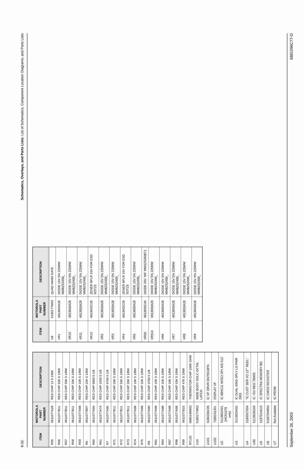
8-32
Sch
emat
ics,
Ove
rlay
s, a
nd
Par
ts L
ists
: Li
st o
f Sch
emat
ics,
Com
pone
nt L
ocat
ion
Dia
gram
s, a
nd P
arts
Lis
ts
Sep
tem
ber
26, 2
003
6881
096C
77-O
R55
0611
077A
28R
ES
CH
IP 1
2 5
1/8W
R56
0611
077B
11R
ES
CH
IP 3
3K 5
1/8
W
R57
0611
077B
11R
ES
CH
IP 3
3K 5
1/8
W
R58
0611
077B
11R
ES
CH
IP 3
3K 5
1/8
W
R59
0611
077A
98R
ES
CH
IP 1
0K 5
1/8
W
R6
0611
077B
07R
ES
CH
IP 2
2K 5
1/8
W
R60
0611
077A
94R
ES
CH
IP 6
800
5 1/
8
R61
0611
077A
74R
ES
CH
IP 1
000
5 1/
8
R7
0611
077A
90R
ES
CH
IP 4
700
5 1/
8
R71
0611
077B
11R
ES
CH
IP 3
3K 5
1/8
W
R72
0611
077B
11R
ES
CH
IP 3
3K 5
1/8
W
R73
0611
077B
11R
ES
CH
IP 3
3K 5
1/8
W
R74
0611
077A
98R
ES
CH
IP 1
0K 5
1/8
W
R75
0611
077A
98R
ES
CH
IP 1
0K 5
1/8
W
R8
0611
077A
90R
ES
CH
IP 4
700
5 1/
8
R81
0611
077A
98R
ES
CH
IP 1
0K 5
1/8
W
R84
0611
077A
98R
ES
CH
IP 1
0K 5
1/8
W
R87
0611
077A
98R
ES
CH
IP 1
0K 5
1/8
W
R98
0611
077A
98R
ES
CH
IP 1
0K 5
1/8
W
R99
0611
077B
15R
ES
CH
IP 4
7K 5
1/8
W
RT
133
0680
149M
02T
HE
RM
IST
OR
CH
IP 1
00K
OH
M
U10
5180
177M
02W
IDE
BO
DY
SO
LC O
CTA
L LA
TC
H
U10
151
8023
6C05
IC V
F D
RV
R S
N75
518F
N
U10
272
8024
2J01
DIS
PLA
Y V
F
U2
5113
802A
01
(HC
N10
78
only
)
IC 6
8HC
11 W
/SC
I SP
I A/D
512
U3
5113
820A
02IC
DU
AL
SIN
G S
PLY
LO
PW
R
2903
U4
5180
057S
04“I
C C
US
T S
ER
I/O
13”
” R
EE
L”
U46
5113
816G
04IC
+5V
RE
G 7
8M05
U5
5197
014A
10IC
SP
EC
TR
A M
EM
OR
Y B
D
U6
5184
704M
54IC
CM
OS
RE
GIS
TE
R
U7
Not
Ava
ilabl
eIC
PR
OM
ITE
MM
OT
OR
OL
A
PA
RT
N
UM
BE
RD
ES
CR
IPT
ION
U8
5180
177M
03Q
UA
D N
AN
D G
AT
E
VR
148
1383
0A28
DIO
DE
15V
5%
225
MW
M
MB
Z52
45B
_
VR
1048
1383
0A28
DIO
DE
15V
5%
225
MW
M
MB
Z52
45B
_
VR
1148
1383
0A28
DIO
DE
15V
5%
225
MW
M
MB
Z52
45B
_
VR
1248
1383
2C28
ZE
NE
R B
PLR
15V
FO
R E
SD
S
OT
23
VR
248
1383
0A28
DIO
DE
15V
5%
225
MW
M
MB
Z52
45B
_
VR
348
1383
0A28
DIO
DE
15V
5%
225
MW
M
MB
Z52
45B
_
VR
448
1383
2C28
ZE
NE
R B
PLR
15V
FO
R E
SD
S
OT
23
VR
548
1383
0A28
DIO
DE
15V
5%
225
MW
M
MB
Z52
45B
_
VR
5048
1383
0C43
DIO
DE
43V
‘M5’
MM
SZ
5260
BT
1
VR
514
4813
830A
28D
IOD
E 1
5V 5
% 2
25M
W
MM
BZ
5245
B_
VR
648
1383
0A28
DIO
DE
15V
5%
225
MW
M
MB
Z52
45B
_
VR
748
1383
0A28
DIO
DE
15V
5%
225
MW
M
MB
Z52
45B
_
VR
848
1383
0A28
DIO
DE
15V
5%
225
MW
M
MB
Z52
45B
_
VR
948
1383
0A28
DIO
DE
15V
5%
225
MW
M
MB
Z52
45B
_
ITE
MM
OTO
RO
LA
P
AR
T
NU
MB
ER
DE
SC
RIP
TIO
N

Sch
emat
ics,
Ove
rlay
s, a
nd
Par
ts L
ists
: Li
st o
f Sch
emat
ics,
Com
pone
nt L
ocat
ion
Dia
gram
s, a
nd P
arts
Lis
ts8-
33
6881
096C
77-O
Sep
tem
ber
26, 2
003
Fig
ure
8-18
. W4,
W5,
and
W7
Con
trol
Hea
d Lo
w-/
Mid
-Pow
er In
terc
onne
ctio
n D
iagr
am
214624
PTT
BUSY
BUS
-
BUS
+
SPAR
E 1
SPAR
E 2
RES
ET
SW B
+
3 374 3852 1918
A+
VF S
ENSE
11
CAB
LE S
IDE
VF S
ENSE
2VF
SEN
SE 2
2
NC
VIP-
OU
T-1
VIP-
OU
T-2
VIP-
OU
T-3/
DEK
-STR
OBE
VIP-
IN-1
VIP-
IN-2
VIP-
IN-3
/DEK
-DAT
A-IN
VF S
ENSE
1
IGN
ITIO
N
B+/A
+
2FI
L AU
D S
HLD
MIC
HI
MIC
LO
HU
B
19VI
P-O
UT-
2/D
EK-D
ATA-
OU
T
VIP-
OU
T-3/
DEK
-STR
OBE
14 17VI
P-IN
-1
VIP-
IN-2
16
VIP-
IN-3
/DEK
-DAT
A-IN
15
DIG
-GN
D
DIG
-GN
D
DIG
-GN
D
W4/
W5/
W7
20 36
SNET
-KEY
SNET
-KID
SNET
-WE
9 20 2112
SWB+
SHIE
LD G
ND
EMER
30 14 31 32 1 34 4024 23
26 6 13
GN
D
GN
D
KEY
SLO
T
VIP SECTION MIC SECTIONRADIO SECTION
RAD
IO S
IDE
11
CO
NTR
OL
HEA
D S
IDE
17
10 22
2623
RES
ET
28 29
SPAR
E 1
DEK
-DAT
A-O
UT
DEK
-CLO
CK
SWB+
SWB+
SWB+
35
VIP-
OU
T-1/
DEK
-CLO
CK
18
1027
MIC
LO
1511
475
SW B
+
B+/A
+
IGN
ITIO
N
16 49
REM
OTE
CO
NTR
OL
HEA
D IN
TER
CO
NN
CEC
T BO
ARD
25
CO
NTR
OL
HEA
D S
IDE
MIC
RO
POH
ON
E H
I (BL
K/YE
L)12
MIC
HI
DET
ECTE
D A
UD
IO
ANAL
OG
GR
OU
ND
PTT/
VIP
IN 1
12
MIC
RO
POH
ON
E LO
(SH
IELD
)
DET
ECTE
D A
UD
IO (B
LK/B
RN
)
MIC
-HI
MIC
-LO
PTT
EMER
G/H
UB
PTT/
HU
B-R
EF
841 7
SPAR
E 1
(BR
OW
N)
13 45 16 46 33 50 17 26 28 29 48 49
50
SPAR
E 2
(RED
)
SW B
+ (Y
ELLO
W)
DIG
ITAL
GR
OU
ND
(BLU
E)
SPEA
KER
LO
(GR
EEN
)
SPEA
KER
HI (
OR
ANG
E)
EMER
GEN
CY
(VIO
LET)
SPEA
KER
HI (
BLK/
OR
G)
SPEA
KER
LO
(BLK
/GR
N)
B+ (G
REE
N)
IGN
ITIO
N (O
RAN
GE)
SPAR
E 2
8 7
484
11 44 43
10 1 23 14 5 21 19 16 17 22 18 24
18
12 11 9 10 23 14 5 21 19 16
DET
ECTE
D A
UD
IO (S
HIE
LD/A
NAL
OG
GR
OU
ND
)
SP 1
(BLK
/GR
N)
SP 1
(SH
IELD
)
BUSY
(BLK
/RED
)
BUS
- (BL
ACK)
BUS
+ (W
HIT
E)
BUS
SHIE
LD (B
ARE)
RES
ET (B
LK/O
RG
)
45
27 3 28
3325
BUSY
MIC
HI
MIC
LO
HU
B
PTT
BUS
-
BUS
+
SPEA
KER
LO
SPEA
KER
HI
EMER
GEN
CY
SPAR
E 1
VIP
OU
T 1
SPAR
E 2
VIP
OU
T 2
27 17 31 3444 27
43 10 47 15
11 925 P
IN R
EMO
TEC
ON
NEC
TOR
(P2)
6 7 13 NC
24
17
9 22 25 NC
11 14
TO C
OM
MAN
D B
OAR
D
NC
NC
NC
NC
22
SPEA
KER
LO
1
3
BUSY
P2
SPEA
KER
HI
EMER
GEN
CY
SWB+
CO
MM
AND
BO
ARD
CO
NN
ECTO
R (P
502)
REM
OTE
RAD
IO IN
TER
CO
NN
ECT
BOAR
D (L
OW
/MID
PO
WER
)
REM
OTE
CO
NTR
OL
HEA
D C
ABLE
12 13
BUS
-
BUS
+
BUS
SHIE
LD
RES
ET
SPAR
E 1
SPAR
E 2
SWB+
18 24 25 13
DIG
ITAL
GR
OU
ND
P9
P1
3513 1 2 E1 E2
NC
NC
TO W
4/W
5/W
7 C
ON
TRO
L H
EAD
JU10
02
R60
8
JU10
04
JU61
4
JU10
08
JU10
01JU10
05
JU10
06
JU60
4
JU10
03
JU10
07
JU51
3
JU65
0
JU51
2
JU63
1JU
632
JU12
JU60
1
JU60
9
JU61
5

8-34
Sch
emat
ics,
Ove
rlay
s, a
nd
Par
ts L
ists
: Li
st o
f Sch
emat
ics,
Com
pone
nt L
ocat
ion
Dia
gram
s, a
nd P
arts
Lis
ts
Sep
tem
ber
26, 2
003
6881
096C
77-O
Fig
ure
8-19
. W4,
W5,
and
W7
Hig
h P
ower
Inte
rcon
nect
ion
Dia
gram
35
IGN
213
IGN
RSS
I/VO
L2
15R
SSI/V
OL
(A2)
RX-
AUD
IO8
7R
X-AU
DIO
TX-A
UD
IO12
8TX
-AU
DIO
FLT-
AUD
IO5
6FL
T_AU
DIO
16
VIP-
IN-3
/DEK
-DAT
A-IN
FIL
AUD
SH
LD
MIC
HI
MIC
LO
HU
B
17VI
P-IN
-1
EMER
GEN
CY
VIP-
IN-2
HU
B
PTT
BUS
-
BUS
+
50
SPAR
E 2
(RED
)
SW B
+ (Y
ELLO
W)
DIG
ITAL
GR
OU
ND
(BLU
E)
SPEA
KER
LO
(GR
EEN
)
SPEA
KER
HI (
OR
ANG
E)
EMER
GEN
CY
(VIO
LET)
SPEA
KER
HI (
BLK/
OR
G)
SPEA
KER
LO
(BLK
/GR
N) B+
(GR
EEN
)
IGN
ITIO
N (O
RAN
GE)
44 27
43 10
SPAR
E 2
NC
NC
31
25 P
IN R
EMO
TEC
ON
NEC
TOR
(P2)
6 7 13
2 E1 E2
SPAR
E 2
13 1
25 NC
11 14 27
12 11 9 10 23 14 5 21 19 16
SPEA
KER
HI
EMER
GEN
CY
SWB+CO
MM
AND
BO
ARD
CO
NN
ECTO
R (P
502)
24 25 13
DIG
ITAL
GR
OU
ND
BUS
-
BUS
+
BUS
SHIE
LD
SPEA
KER
LO
SPEA
KER
HI
17SP
ARE
1
34
17 22 18 24 25
CO
NTR
OL
HEA
D S
IDEM
ICR
OPO
HO
NE
HI (
BLK/
YEL)
12M
IC H
I
DET
ECTE
D A
UD
IO
ANAL
OG
GR
OU
ND
PTT
12
MIC
RO
POH
ON
E LO
(SH
IELD
)
DET
ECTE
D A
UD
IO (B
LK/B
RN
)
DET
ECTE
D A
UD
IO (S
HIE
LD/A
NAL
OG
GR
OU
ND
)
SP 1
(BLK
/GR
N)
SP 1
(SH
IELD
)
BUSY
(BLK
/RED
)
REM
OTE
RAD
IO IN
TER
CO
NN
ECT
BOAR
D (H
IGH
PO
WER
)
REM
OTE
CO
NTR
OL
HEA
D C
ABLE
12 13 45
27 3 28
RES
ET
SPAR
E 1
BUSY
SWB+
18
28 29 48 49 11
CO
NTR
OL
HEA
D S
IDE
17
10 22
2623
RES
ET28 29
SPAR
E 1
SPAR
E 2
8 7
48
47 15
11 9 10 1 23
NC
24
21
9 22
IGN
ITIO
N
16 49
REM
OTE
CO
NTR
OL
HEA
D IN
TER
CO
NN
CEC
T BO
ARD
W4/
W5/
W7
20 36
SNET
-KEY
SNET
-KID
SNET
-WE
9 20 2112
SWB+
MIC
-HI
MIC
-LO
PTT
EMER
G/H
UB
BUS
- (BL
ACK)
BUS
+ (W
HIT
E)
BUS
SHIE
LD (B
ARE)
RES
ET (B
LK/O
RG
)
SPAR
E 1
(BR
OW
N)
13 45 16
3325
50
MIC
HI
MIC
LO
VIP SECTION MIC SECTIONRADIO SECTION
RAD
IO S
IDE
CAB
LE S
IDE
VF S
ENSE
2VF
SEN
SE 2
2
NC
VIP-
OU
T-1
VIP-
OU
T-2
VIP-
OU
T-3/
DEK
-STR
OBE
VIP-
IN-1
VIP-
IN-2
VIP-
IN-3
/DEK
-DAT
A-IN
DEK
-DAT
A-O
UT
DEK
-CLO
CK
SWB+
SWB+
4
11 44 43 1027
MIC
LO
15
14 5
5
19 16
15
DIG
-GN
D
DIG
-GN
D
DIG
-GN
D
214624
PTT
BUSY
BUS
-
BUS
+
SPAR
E 1
SPAR
E 2
RES
ET
SW B
+
SHIE
LD G
ND
EMER
30 14
PTT/
HU
B-R
EF
841 7 4024 23
26
46 33
GN
D
17 26
22
SPEA
KER
LO
1
3
3 374 3852 1918
A+ VF S
ENSE
11
VF S
ENSE
1
IGN
ITIO
N
B+/A
+
2
SWB+
35
VIP-
OU
T-1/
DEK
-CLO
CK
18 19VI
P-O
UT-
2/D
EK-D
ATA-
OU
T
VIP-
OU
T-3/
DEK
-STR
OBE
1411
47
KEY
SLO
T
SW B
+
B+/A
+
A+30
20A+
RES
ET
BUSY
BUS
-
BUS
+
10 28
ANA-
GN
D
DIG
-GN
D
19.
6V
PTT
MIC
HI
MIC
LO
TO W
4/W
5/W
7 C
ON
TRO
L H
EAD
BUSY
31 32 1 34
NC
NC
NC
NC
6 13G
ND
JU64
3
JU63
6
JU60
1
JU60
9
JU64
2
JU10
04
JU64
4
JU64
1
JU10
01
JU60
8
JU60
7
JU66
2
JU60
6
JU66
3
JU65
9
JU61
6
JU10
03
JU10
07
JU64
0
JU65
3
JU63
2
JU65
7JU
633
JU61
4JU
645
JU63
9
JU65
5
JU10
02
JU61
5
JU65
0JU
646
JU10
06
JU10
08
JU60
4
JU10
05
JU63
8
JU63
7
JU63
0

Sch
emat
ics,
Ove
rlay
s, a
nd
Par
ts L
ists
: Li
st o
f Sch
emat
ics,
Com
pone
nt L
ocat
ion
Dia
gram
s, a
nd P
arts
Lis
ts8-
35
6881
096C
77-O
Sep
tem
ber
26, 2
003
Fig
ure
8-20
. W5
and
W7
Con
trol
Hea
d In
terf
ace
Boa
rd S
chem
atic
33 B
USY
46 P
TT
12 M
IC-H
I13
MIC
-L0
45 H
UB
9000
CAB
LEIN
TER
FAC
E C
ON
N.
P010
0
HLN
6432
D W
5/W
7 C
ON
TRO
L H
EAD
INTE
RFA
CE
BO
AR
D
MAE
PF-2
3570
-A
CO
NTR
OL
HEA
DC
ON
NEC
TOR
J010
3M
IC-H
I 27
MIC
-LO
3H
UB
28
JU10
05*
PTT
2
4
JU10
06*
BUSY
25
17 B
US+
BUS+
22
50 B
US
BUS
10
26 R
ESET
RES
ET 2
3
28 S
PAR
E
1SP
ARE
1
8
29 S
PAR
E
2SP
ARE
2
7
47 A
+A+
5
15 IG
NIG
N 1
1
48 S
WB+
SWB+
4 12
11 S
PKR
LO
44 S
PKR
H
I43
SPK
R
HI
10 S
PKR
LO
27 E
MER
GEN
CY
VR10
03**
VR10
01
VR10
0215
V
15V
VF S
ENSE
1
1VF
SEN
SE 2
2
JU10
01*
16 S
HIE
LD G
ND
14 V
F SE
NSE
1JU
1008
49 D
IGIT
AL G
ND
30 A
+31
VF
SEN
SE 2
32
JU10
07
26KE
Y SL
OT
6 13G
ND
GN
D
2 VI
P-O
UT-
1VI
P-O
UT-
1/D
EK-C
LOC
K 18
1 VI
P-O
UT-
2VI
P-O
UT-
2/D
EK-D
ATA-
OU
T 19
34 V
IP-O
UT-
3/D
EK-S
TRO
BEVI
P-O
UT-
3/D
EK-S
TRO
BE 1
44
VIP-
IN-1
VIP-
IN-1
17
3 VI
P-IN
-2VI
P-IN
-2 1
637
VIP
-IN-3
/DEK
-DAT
A-IN
VIP-
IN-3
/DEK
-DAT
A-IN
15
5 D
EK-D
ATA-
OU
T38
DEK
-CLO
CK
18 S
WB+
19 S
WB+
35 S
WB+
20 D
IG-G
ND
21 D
IG-G
ND
36 D
IG-G
ND
9SN
ET-K
EY
20SN
ET-K
ID
21SN
ET-W
E
* = P
ARTS
NO
T PL
ACED
** =
010
5950
T92
ON
LY41
SW
B+8
MIC
-HI
7 M
IC-L
O
24 P
TT
40 E
MER
G/H
UB
23 P
TT/H
UB-
REF
JU10
02*
JU10
03*
JU10
04*
MIC SECTIONVIP SECTIONRADIO SECTION

8-36
Sch
emat
ics,
Ove
rlay
s, a
nd
Par
ts L
ists
: Li
st o
f Sch
emat
ics,
Com
pone
nt L
ocat
ion
Dia
gram
s, a
nd P
arts
Lis
ts
Sep
tem
ber
26, 2
003
6881
096C
77-O
Fig
ure
8-21
. HLN
6432
D W
5/W
7 C
ontr
ol H
ead
Inte
rfac
e B
oard
Com
pone
nt L
ocat
ion
Dia
gram
JU1002
JU1003
JU1006
VR10
03
JU1004JU1005
VR10
01VR
1002
JU1007
JU1008
JU1001
HL
N64
32D
W5/
W7
Par
ts L
ist
Item
Mo
toro
laP
art
Nu
mb
erD
escr
ipti
on
JU10
01N
OT
PLA
CE
D64
AM
DU
MM
Y P
AR
T N
UM
BE
R
JU10
02N
OT
PLA
CE
D64
AM
DU
MM
Y P
AR
T N
UM
BE
R
JU10
03N
OT
PLA
CE
D64
AM
DU
MM
Y P
AR
T N
UM
BE
R
JU10
04N
OT
PLA
CE
D64
AM
DU
MM
Y P
AR
T N
UM
BE
R
JU10
05N
OT
PLA
CE
D64
AM
DU
MM
Y P
AR
T N
UM
BE
R
JU10
06N
OT
PLA
CE
D64
AM
DU
MM
Y P
AR
T N
UM
BE
R
JU10
0706
1107
7A01
RE
S C
HIP
JU
MP
ER
JU10
0806
1107
7A01
RE
S C
HIP
JU
MP
ER
VR
1001
4813
830A
28D
IOD
E 1
5V 5
% 2
25M
W
MM
BZ
5245
B_
VR
1002
4813
830A
28D
IOD
E 1
5V 5
% 2
25M
W
MM
BZ
5245
B_
VR
1003
NO
TP
LAC
ED
64A
M D
UM
MY
PA
RT
NU
MB
ER

Sch
emat
ics,
Ove
rlay
s, a
nd
Par
ts L
ists
: Li
st o
f Sch
emat
ics,
Com
pone
nt L
ocat
ion
Dia
gram
s, a
nd P
arts
Lis
ts8-
37
6881
096C
77-O
Sep
tem
ber
26, 2
003
Fig
ure
8-22
. HLN
6401
A C
ontr
ol H
ead
Inte
rcon
nect
Boa
rd, (
Das
h-M
ount
)
1 2 3 4 5 6 7 8 9 10 11 12 13 14 15 16 17 18 19 20 21 22 23 24 25 26 27 28
NC
NC
MIC
-LO
WN
C
NC
J103
P
502
HL
N64
01A
CO
NT
RO
L H
EA
D IN
TE
RC
ON
NE
CT
BO
AR
D(D
ash
Mo
un
t)
MA
EP
F-2
3575
-O
1 3 7 31 30 28 27 14 23 22 21 4 5 8 10 12 13 18 17 16 15 25 11 2 9 32 6 29 19 20 24 26 33 34 35 36 37 38
NC
NC
NC
NC
NC
NC
NC
NC
NC
NC
NC
NC
NC
NC
NC
NC
KE
YE
D-S
LOT
KE
YE
D-S
LOT
NC
NC
NC
NC
NC
NC
NO
TE
CR
10
JU11
NO
TE
JU
10N
OT
E
SW
B+
A+
DIG
-GN
D
SP
AR
E-2
SP
AR
E-1
SE
RIA
L B
US
RE
SE
TB
US
-IG
N
VIP
-OU
T-1
VIP
-OU
T-2
S.N
ET
_KID
/PR
OG
-VP
P
S.N
ET
_WE
/PR
OG
-RX
DB
US
+S
.NE
T_K
EY
/PR
OG
-TX
D
MIC
PT
T/P
RO
G-R
ES
ET
BU
SY
MIC
-HI/P
RO
G-M
OD
-CO
NT
RO
LH
UB
/PR
OG
BU
SY
NO
TE
: NO
T C
OM
PA
TIB
LE W
ITH
S
PE
CT
RA
E J
U10
, JU
11, C
R10
INS
TA
LLE
D
FO
R A
VL
OP
TIO
N.
TR
AC
E C
UT
ON
LY W
HE
N
CR
10 IN
ST
ALL
ED
.

8-38
Sch
emat
ics,
Ove
rlay
s, a
nd
Par
ts L
ists
: Li
st o
f Sch
emat
ics,
Com
pone
nt L
ocat
ion
Dia
gram
s, a
nd P
arts
Lis
ts
Sep
tem
ber
26, 2
003
6881
096C
77-O
Fig
ure
8-23
. HLN
6486
D/E
Hig
h P
ower
Sta
ndar
d In
terc
onne
ct B
oard
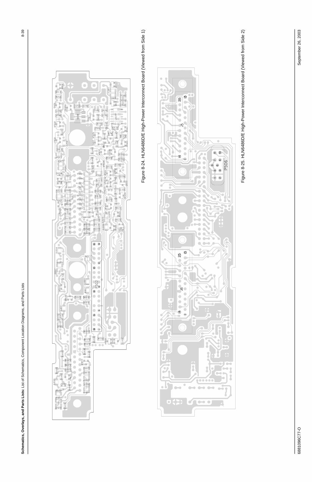
Sch
emat
ics,
Ove
rlay
s, a
nd
Par
ts L
ists
: Li
st o
f Sch
emat
ics,
Com
pone
nt L
ocat
ion
Dia
gram
s, a
nd P
arts
Lis
ts8-
39
6881
096C
77-O
Sep
tem
ber
26, 2
003
Fig
ure
8-24
. HLN
6486
D/E
Hig
h-P
ower
Inte
rcon
nect
Boa
rd (
Vie
wed
from
Sid
e 1)
Fig
ure
8-25
. HLN
6486
D/E
Hig
h-P
ower
Inte
rcon
nect
Boa
rd (
Vie
wed
from
Sid
e 2)
13
24
5 67 8
9 10

8-40
Sch
emat
ics,
Ove
rlay
s, a
nd
Par
ts L
ists
: Li
st o
f Sch
emat
ics,
Com
pone
nt L
ocat
ion
Dia
gram
s, a
nd P
arts
Lis
ts
Sep
tem
ber
26, 2
003
6881
096C
77-O
HL
N64
86E
Sta
nd
ard
Inte
rco
nn
ect
Par
ts L
ist
ITE
MM
OT
OR
OL
A
PA
RT
N
UM
BE
RD
ES
CR
IPT
ION
C75
021
1374
0B49
CA
P C
HIP
RE
EL
CL1
+/-
30 1
00
C75
121
1374
1N69
CA
P C
HIP
CL2
X7R
10%
10
0000
C75
221
1374
0B49
CA
P C
HIP
RE
EL
CL1
+/-
30 1
00
C75
421
1374
0B49
CA
P C
HIP
RE
EL
CL1
+/-
30 1
00
C75
521
1374
0B49
CA
P C
HIP
RE
EL
CL1
+/-
30 1
00
C75
621
1374
0B49
CA
P C
HIP
RE
EL
CL1
+/-
30 1
00
C75
721
1374
0B49
CA
P C
HIP
RE
EL
CL1
+/-
30 1
00
C76
321
1374
1N45
CA
P C
HIP
CL2
X7R
10%
100
00
C76
421
1374
0B49
CA
P C
HIP
RE
EL
CL1
+/-
30 1
00
C76
521
1374
0B49
CA
P C
HIP
RE
EL
CL1
+/-
30 1
00
C76
821
1374
0B49
CA
P C
HIP
RE
EL
CL1
+/-
30 1
00
C77
021
1374
0B49
CA
P C
HIP
RE
EL
CL1
+/-
30 1
00
C77
121
1374
0B49
CA
P C
HIP
RE
EL
CL1
+/-
30 1
00
C77
221
1374
0B49
CA
P C
HIP
RE
EL
CL1
+/-
30 1
00
C77
321
1374
0B49
CA
P C
HIP
RE
EL
CL1
+/-
30 1
00
C77
421
1374
0B65
CA
P C
HIP
RE
EL
CL1
+/-
30 4
70
C77
521
1374
0B65
CA
P C
HIP
RE
EL
CL1
+/-
30 4
70
C77
621
1374
0B65
CA
P C
HIP
RE
EL
CL1
+/-
30 4
70
C77
721
1374
0B65
CA
P C
HIP
RE
EL
CL1
+/-
30 4
70
H00
0103
0013
9581
SC
R M
CH
4-4
0X5/
16 P
HLP
AN
S
TL
H00
0203
0013
9581
SC
R M
CH
4-4
0X5/
16 P
HLP
AN
S
TL
H00
0303
0013
9581
SC
R M
CH
4-4
0X5/
16 P
HLP
AN
S
TL
H00
0403
0013
9581
SC
R M
CH
4-4
0X5/
16 P
HLP
AN
S
TL
J000
509
8015
9P02
CO
NN
EC
TO
R 2
5-P
IN
J000
609
8015
9P02
CO
NN
EC
TO
R 2
5-P
IN
JU60
106
1107
7A01
RE
S C
HIP
JU
MP
ER
JU60
406
1107
7A01
RE
S C
HIP
JU
MP
ER
JU60
606
1107
7A01
RE
S C
HIP
JU
MP
ER
JU60
706
1107
7A01
RE
S C
HIP
JU
MP
ER
JU60
806
1107
7A01
RE
S C
HIP
JU
MP
ER
JU60
906
1107
7A01
RE
S C
HIP
JU
MP
ER
JU61
306
1107
7A01
RE
S C
HIP
JU
MP
ER
JU61
806
1107
7A01
RE
S C
HIP
JU
MP
ER
JU61
906
1107
7A01
RE
S C
HIP
JU
MP
ER
JU62
006
1107
7A01
RE
S C
HIP
JU
MP
ER
JU62
106
1107
7A01
RE
S C
HIP
JU
MP
ER
JU62
206
1107
7A01
RE
S C
HIP
JU
MP
ER
JU62
306
1107
7A01
RE
S C
HIP
JU
MP
ER
JU62
606
1107
7A01
RE
S C
HIP
JU
MP
ER
JU62
906
1107
7A01
RE
S C
HIP
JU
MP
ER
JU63
006
1107
7A01
RE
S C
HIP
JU
MP
ER
JU63
206
1107
7A01
RE
S C
HIP
JU
MP
ER
JU63
606
1107
7A01
RE
S C
HIP
JU
MP
ER
JU63
706
1107
7A01
RE
S C
HIP
JU
MP
ER
JU63
806
1107
7A01
RE
S C
HIP
JU
MP
ER
JU63
906
1107
7A01
RE
S C
HIP
JU
MP
ER
JU64
006
1107
7A01
RE
S C
HIP
JU
MP
ER
JU64
406
1107
7A01
RE
S C
HIP
JU
MP
ER
JU64
506
1107
7A01
RE
S C
HIP
JU
MP
ER
JU64
606
1107
7A01
RE
S C
HIP
JU
MP
ER
JU65
206
1107
7A01
RE
S C
HIP
JU
MP
ER
JU65
306
1107
7A01
RE
S C
HIP
JU
MP
ER
JU65
506
1107
7A01
RE
S C
HIP
JU
MP
ER
JU65
706
1107
7A01
RE
S C
HIP
JU
MP
ER
JU65
806
1107
7A01
RE
S C
HIP
JU
MP
ER
JU66
206
1107
7A01
RE
S C
HIP
JU
MP
ER
JU66
406
1107
7A01
RE
S C
HIP
JU
MP
ER
JU66
506
1107
7A01
RE
S C
HIP
JU
MP
ER
JU66
606
1107
7A01
RE
S C
HIP
JU
MP
ER
JU67
106
1107
7A01
RE
S C
HIP
JU
MP
ER
JU67
206
1107
7A01
RE
S C
HIP
JU
MP
ER
JU67
306
1107
7A01
RE
S C
HIP
JU
MP
ER
JU67
406
1107
7A01
RE
S C
HIP
JU
MP
ER
ITE
MM
OTO
RO
LA
P
AR
T
NU
MB
ER
DE
SC
RIP
TIO
N
P05
0228
8026
7M04
PLU
G R
IGH
T A
NG
LE H
DR
38
PO
S
P05
0628
8006
8M01
HE
AD
ER
MIC
R60
106
1107
7A01
RE
S C
HIP
JU
MP
ER
R60
206
1107
7A01
RE
S C
HIP
JU
MP
ER
R60
306
1107
7A01
RE
S C
HIP
JU
MP
ER
R61
406
1107
7A98
RE
S C
HIP
10K
5 1
/8W
VR
600
4813
830A
28D
IOD
E 1
5V 5
% 2
25M
W
MM
BZ
5245
B_
VR
601
4813
830A
28D
IOD
E 1
5V 5
% 2
25M
W
MM
BZ
5245
B_
VR
602
4813
830A
28D
IOD
E 1
5V 5
% 2
25M
W
MM
BZ
5245
B_
VR
603
4813
830A
28D
IOD
E 1
5V 5
% 2
25M
W
MM
BZ
5245
B_
VR
604
4813
830A
28D
IOD
E 1
5V 5
% 2
25M
W
MM
BZ
5245
B_
VR
605
4813
830A
28D
IOD
E 1
5V 5
% 2
25M
W
MM
BZ
5245
B_
VR
606
4813
830A
28D
IOD
E 1
5V 5
% 2
25M
W
MM
BZ
5245
B_
VR
610
4813
830A
28D
IOD
E 1
5V 5
% 2
25M
W
MM
BZ
5245
B_
VR
611
4813
830A
28D
IOD
E 1
5V 5
% 2
25M
W
MM
BZ
5245
B_
VR
612
4813
830A
28D
IOD
E 1
5V 5
% 2
25M
W
MM
BZ
5245
B_
VR
613
4813
830A
28D
IOD
E 1
5V 5
% 2
25M
W
MM
BZ
5245
B_
VR
615
4813
830A
28D
IOD
E 1
5V 5
% 2
25M
W
MM
BZ
5245
B_
VR
616
4813
830A
28D
IOD
E 1
5V 5
% 2
25M
W
MM
BZ
5245
B_
VR
617
4813
830A
28D
IOD
E 1
5V 5
% 2
25M
W
MM
BZ
5245
B_
VR
618
4813
830A
28D
IOD
E 1
5V 5
% 2
25M
W
MM
BZ
5245
B_
VR
623
4813
830A
28D
IOD
E 1
5V 5
% 2
25M
W
MM
BZ
5245
B_
VR
624
4813
830A
28D
IOD
E 1
5V 5
% 2
25M
W
MM
BZ
5245
B_
ITE
MM
OTO
RO
LA
PA
RT
N
UM
BE
RD
ES
CR
IPT
ION
VR
625
4813
832C
28Z
EN
ER
BP
LR 1
5V F
OR
ES
D
SO
T23
VR
626
4813
832C
28Z
EN
ER
BP
LR 1
5V F
OR
ES
D
SO
T23
VR
627
4813
832C
28Z
EN
ER
BP
LR 1
5V F
OR
ES
D
SO
T23
VR
628
4813
832C
28Z
EN
ER
BP
LR 1
5V F
OR
ES
D
SO
T23
ITE
MM
OT
OR
OL
A
PAR
T
NU
MB
ER
DE
SC
RIP
TIO
N

Sch
emat
ics,
Ove
rlay
s, a
nd
Par
ts L
ists
: Li
st o
f Sch
emat
ics,
Com
pone
nt L
ocat
ion
Dia
gram
s, a
nd P
arts
Lis
ts8-
41
6881
096C
77-O
Sep
tem
ber
26, 2
003
Fig
ure
8-26
. HLN
6574
E W
3 C
ontr
ol H
ead
Hig
h-P
ower
Inte
rcon
nect
Boa
rd S
chem
atic
Des
ign
8-42
Sch
emat
ics,
Ove
rlay
s, a
nd
Par
ts L
ists
: Li
st o
f Sch
emat
ics,
Com
pone
nt L
ocat
ion
Dia
gram
s, a
nd P
arts
Lis
ts
Sep
tem
ber
26, 2
003
6881
096C
77-O
Fig
ure
8-27
. HLN
6574
E W
3 H
igh
Pow
er In
terc
onne
ct B
oard
Com
pone
nt L
ocat
ion
Dia
gram
s
MA
EP
F-2
5697
-O
MA
EP
F-2
5698
-O
Sch
emat
ics,
Ove
rlay
s, a
nd
Par
ts L
ists
: Li
st o
f Sch
emat
ics,
Com
pone
nt L
ocat
ion
Dia
gram
s, a
nd P
arts
Lis
ts8-
43
6881
096C
77-O
Sep
tem
ber
26, 2
003
HL
N65
74E
W3
Hig
h-P
ow
er In
terc
on
nec
t P
arts
Lis
t
ITE
MM
OTO
RO
LA
PA
RT
N
UM
BE
RD
ES
CR
IPT
ION
C1
2113
740B
65C
AP
CH
IP R
EE
L C
L1 +
/-30
470
C10
2113
740B
65C
AP
CH
IP R
EE
L C
L1 +
/-30
470
C11
2113
740B
65C
AP
CH
IP R
EE
L C
L1 +
/-30
470
C12
2113
740B
65C
AP
CH
IP R
EE
L C
L1 +
/-30
470
C13
2113
740B
65C
AP
CH
IP R
EE
L C
L1 +
/-30
470
C14
2113
740B
65C
AP
CH
IP R
EE
L C
L1 +
/-30
470
C15
2113
740B
49C
AP
CH
IP R
EE
L C
L1 +
/-30
100
C16
2113
740B
49C
AP
CH
IP R
EE
L C
L1 +
/-30
100
C17
2113
740B
49C
AP
CH
IP R
EE
L C
L1 +
/-30
100
C18
2113
740B
49C
AP
CH
IP R
EE
L C
L1 +
/-30
100
C19
2113
740B
49C
AP
CH
IP R
EE
L C
L1 +
/-30
100
C2
2113
740B
65C
AP
CH
IP R
EE
L C
L1 +
/-30
470
C20
2113
740B
49C
AP
CH
IP R
EE
L C
L1 +
/-30
100
C21
2113
740B
49C
AP
CH
IP R
EE
L C
L1 +
/-30
100
C22
2113
740B
49C
AP
CH
IP R
EE
L C
L1 +
/-30
100
C23
2113
740B
49C
AP
CH
IP R
EE
L C
L1 +
/-30
100
C24
2113
740B
49C
AP
CH
IP R
EE
L C
L1 +
/-30
100
C25
2113
740B
49C
AP
CH
IP R
EE
L C
L1 +
/-30
100
C26
2113
740B
65C
AP
CH
IP R
EE
L C
L1 +
/-30
470
C27
2113
740B
65C
AP
CH
IP R
EE
L C
L1 +
/-30
470
C28
2113
740B
65C
AP
CH
IP R
EE
L C
L1 +
/-30
470
C29
2113
740B
65C
AP
CH
IP R
EE
L C
L1 +
/-30
470
C3
2113
740B
65C
AP
CH
IP R
EE
L C
L1 +
/-30
470
C30
2113
740B
65C
AP
CH
IP R
EE
L C
L1 +
/-30
470
C31
2113
741N
45C
AP
CH
IP C
L2 X
7R 1
0% 1
0000
C32
2113
741N
45C
AP
CH
IP C
L2 X
7R 1
0% 1
0000
C33
2113
741N
69C
AP
CH
IP C
L2 X
7R 1
0%
1000
00
C34
2113
741N
69C
AP
CH
IP C
L2 X
7R 1
0%
1000
00
C35
2311
049J
26C
AP
TA
NT
CH
IP 1
0 20
16
C37
2311
049J
26C
AP
TA
NT
CH
IP 1
0 20
16
C38
2311
049A
37C
AP
TA
NT
CH
IP 1
20
20
C4
2113
740B
65C
AP
CH
IP R
EE
L C
L1 +
/-30
470
C5
2113
740B
49C
AP
CH
IP R
EE
L C
L1 +
/-30
100
C6
2113
740B
49C
AP
CH
IP R
EE
L C
L1 +
/-30
100
C7
2113
740B
49C
AP
CH
IP R
EE
L C
L1 +
/-30
100
C8
2113
740B
49C
AP
CH
IP R
EE
L C
L1 +
/-30
100
C9
2113
740B
49C
AP
CH
IP R
EE
L C
L1 +
/-30
100
CR
148
1383
3C10
DIO
DE
GE
N P
UR
70V
M
MB
D60
50
CR
248
1383
3C10
DIO
DE
GE
N P
UR
70V
M
MB
D60
50
CR
348
1383
3C10
DIO
DE
GE
N P
UR
70V
M
MB
D60
50
CR
448
1383
3C10
DIO
DE
GE
N P
UR
70V
M
MB
D60
50
CR
548
1383
3C10
DIO
DE
GE
N P
UR
70V
M
MB
D60
50
CR
648
1383
3C10
DIO
DE
GE
N P
UR
70V
M
MB
D60
50
CR
748
1383
3C10
DIO
DE
GE
N P
UR
70V
M
MB
D60
50
CR
8N
OT
PLA
CE
D64
AM
DU
MM
Y P
AR
T N
UM
BE
R
H00
0103
0013
9581
SC
R M
CH
4-4
0X5/
16 P
HLP
AN
S
TL
H00
0203
0013
9581
SC
R M
CH
4-4
0X5/
16 P
HLP
AN
S
TL
H00
0303
0013
9581
SC
R M
CH
4-4
0X5/
16 P
HLP
AN
S
TL
H00
0403
0013
9581
SC
R M
CH
4-4
0X5/
16 P
HLP
AN
S
TL
HU
3N
OT
PLA
CE
D64
AM
DU
MM
Y P
AR
T N
UM
BE
R
J509
8015
9P02
CO
NN
EC
TO
R 2
5-P
IN
J609
8015
9P02
CO
NN
EC
TO
R 2
5-P
IN
JU1
0611
077A
01R
ES
CH
IP J
UM
PE
R
JU10
NO
TP
LAC
ED
64A
M D
UM
MY
PA
RT
NU
MB
ER
JU11
0611
077A
01R
ES
CH
IP J
UM
PE
R
JU12
0611
077A
01R
ES
CH
IP J
UM
PE
R
JU13
0611
077A
01R
ES
CH
IP J
UM
PE
R
JU14
0611
077A
01R
ES
CH
IP J
UM
PE
R
ITE
MM
OT
OR
OL
A
PAR
T
NU
MB
ER
DE
SC
RIP
TIO
N
JU15
NO
TP
LAC
ED
64A
M D
UM
MY
PA
RT
NU
MB
ER
JU16
0611
077A
01R
ES
CH
IP J
UM
PE
R
JU17
0611
077A
01R
ES
CH
IP J
UM
PE
R
JU18
0611
077A
01R
ES
CH
IP J
UM
PE
R
JU19
0611
077A
01R
ES
CH
IP J
UM
PE
R
JU2
0611
077A
01R
ES
CH
IP J
UM
PE
R
JU20
0611
077A
01R
ES
CH
IP J
UM
PE
R
JU21
0611
077A
01R
ES
CH
IP J
UM
PE
R
JU22
0611
077A
01R
ES
CH
IP J
UM
PE
R
JU23
0611
077A
01R
ES
CH
IP J
UM
PE
R
JU24
NO
TP
LAC
ED
64A
M D
UM
MY
PA
RT
NU
MB
ER
JU25
0611
077A
01R
ES
CH
IP J
UM
PE
R
JU26
0611
077A
01R
ES
CH
IP J
UM
PE
R
JU27
0611
077A
01R
ES
CH
IP J
UM
PE
R
JU28
0611
077A
01R
ES
CH
IP J
UM
PE
R
JU29
0611
077A
01R
ES
CH
IP J
UM
PE
R
JU30
0611
077A
01R
ES
CH
IP J
UM
PE
R
JU31
0611
077A
01R
ES
CH
IP J
UM
PE
R
JU32
0611
077A
01R
ES
CH
IP J
UM
PE
R
JU33
0611
077A
01R
ES
CH
IP J
UM
PE
R
JU34
0611
077A
01R
ES
CH
IP J
UM
PE
R
JU35
0611
077A
01R
ES
CH
IP J
UM
PE
R
JU36
0611
077A
01R
ES
CH
IP J
UM
PE
R
JU37
0611
077A
01R
ES
CH
IP J
UM
PE
R
JU38
0611
077A
01R
ES
CH
IP J
UM
PE
R
JU39
0611
077A
01R
ES
CH
IP J
UM
PE
R
JU4
2113
741N
69C
AP
CH
IP C
L2 X
7R 1
0%
1000
00
JU40
0611
077A
01R
ES
CH
IP J
UM
PE
R
JU41
NO
TP
LAC
ED
64A
M D
UM
MY
PA
RT
NU
MB
ER
JU42
0611
077A
01R
ES
CH
IP J
UM
PE
R
JU43
0611
077A
01R
ES
CH
IP J
UM
PE
R
JU44
0611
077A
01R
ES
CH
IP J
UM
PE
R
JU45
0611
077A
01R
ES
CH
IP J
UM
PE
R
ITE
MM
OT
OR
OL
A
PA
RT
N
UM
BE
RD
ES
CR
IPT
ION
JU46
0611
077A
01R
ES
CH
IP J
UM
PE
R
JU47
0611
077A
01R
ES
CH
IP J
UM
PE
R
JU48
0611
077A
01R
ES
CH
IP J
UM
PE
R
JU49
0611
077A
01R
ES
CH
IP J
UM
PE
R
JU5
0611
077A
74R
ES
CH
IP 1
000
5 1/
8
JU50
0611
077A
01R
ES
CH
IP J
UM
PE
R
JU51
0611
077A
01R
ES
CH
IP J
UM
PE
R
JU52
NO
TP
LAC
ED
64A
M D
UM
MY
PA
RT
NU
MB
ER
JU53
0611
077A
01R
ES
CH
IP J
UM
PE
R
JU54
0611
077A
01R
ES
CH
IP J
UM
PE
R
JU55
NO
TP
LAC
ED
64A
M D
UM
MY
PA
RT
NU
MB
ER
JU56
0611
077A
01R
ES
CH
IP J
UM
PE
R
JU57
NO
TP
LAC
ED
64A
M D
UM
MY
PA
RT
NU
MB
ER
JU58
NO
TP
LAC
ED
64A
M D
UM
MY
PA
RT
NU
MB
ER
JU59
0611
077A
01R
ES
CH
IP J
UM
PE
R
JU6
NO
TP
LAC
ED
64A
M D
UM
MY
PA
RT
NU
MB
ER
JU60
NO
TP
LAC
ED
64A
M D
UM
MY
PA
RT
NU
MB
ER
JU61
NO
TP
LAC
ED
64A
M D
UM
MY
PA
RT
NU
MB
ER
JU62
0611
077A
01R
ES
CH
IP J
UM
PE
R
JU7
NO
TP
LAC
ED
64A
M D
UM
MY
PA
RT
NU
MB
ER
JU8
NO
TP
LAC
ED
64A
M D
UM
MY
PA
RT
NU
MB
ER
JU9
NO
TP
LAC
ED
64A
M D
UM
MY
PA
RT
NU
MB
ER
P50
228
8026
7M04
PLU
G R
IGH
T A
NG
LE H
DR
38
PO
S
P50
628
8006
8M01
HE
AD
ER
MIC
Q2
4880
048M
01T
ST
R N
PN
DIG
47K
/47K
Q3
4880
052M
01T
ST
R N
PN
DR
LNG
TN
MX
TA27
Q4
4813
821A
32T
ST
R P
-CH
PW
R F
ET
60V
5A
Q5
4880
052M
01T
ST
R N
PN
DR
LNG
TN
MX
TA27
R1
NO
TP
LAC
ED
64A
M D
UM
MY
PA
RT
NU
MB
ER
R10
0611
077B
15R
ES
CH
IP 4
7K 5
1/8
W
R11
0611
077B
15R
ES
CH
IP 4
7K 5
1/8
W
R12
0611
077B
23R
ES
CH
IP 1
00K
5 1
/8W
R13
0611
077A
54R
ES
CH
IP 1
50 5
1/8
W
ITE
MM
OTO
RO
LA
P
AR
T
NU
MB
ER
DE
SC
RIP
TIO
N
8-44
Sch
emat
ics,
Ove
rlay
s, a
nd
Par
ts L
ists
: Li
st o
f Sch
emat
ics,
Com
pone
nt L
ocat
ion
Dia
gram
s, a
nd P
arts
Lis
ts
Sep
tem
ber
26, 2
003
6881
096C
77-O
R14
0611
077A
74R
ES
CH
IP 1
000
5 1/
8
R15
0611
077A
74R
ES
CH
IP 1
000
5 1/
8
R2
NO
TP
LAC
ED
64A
M D
UM
MY
PA
RT
NU
MB
ER
R3
0611
077A
98R
ES
CH
IP 1
0K 5
1/8
W
R4
0611
077A
98R
ES
CH
IP 1
0K 5
1/8
W
R5
0611
077A
98R
ES
CH
IP 1
0K 5
1/8
W
R6
0611
077A
98R
ES
CH
IP 1
0K 5
1/8
W
R7
0611
077B
15R
ES
CH
IP 4
7K 5
1/8
W
R9
0611
077B
15R
ES
CH
IP 4
7K 5
1/8
W
U1
5113
806A
05IC
FLI
P-F
LOP,
DU
AL
D
U2
5113
806A
37IC
SC
HM
ITT
TR
IGG
ER
,HE
X
U3
5113
816A
19IC
AD
J LO
DR
OP
OU
T P
OS
R
EG
.8A
VR
148
1383
0A28
DIO
DE
15V
5%
225
MW
M
MB
Z52
45B
_
VR
1048
1383
0A28
DIO
DE
15V
5%
225
MW
M
MB
Z52
45B
_
VR
1148
1383
0A28
DIO
DE
15V
5%
225
MW
M
MB
Z52
45B
_
VR
1248
1383
0A28
DIO
DE
15V
5%
225
MW
M
MB
Z52
45B
_
VR
1348
1383
0A28
DIO
DE
15V
5%
225
MW
M
MB
Z52
45B
_
VR
1448
1383
0A28
DIO
DE
15V
5%
225
MW
M
MB
Z52
45B
_
VR
1548
1383
0A28
DIO
DE
15V
5%
225
MW
M
MB
Z52
45B
_
VR
1648
1383
0A28
DIO
DE
15V
5%
225
MW
M
MB
Z52
45B
_
VR
1748
1383
0A28
DIO
DE
15V
5%
225
MW
M
MB
Z52
45B
_
VR
1848
1383
0A28
DIO
DE
15V
5%
225
MW
M
MB
Z52
45B
_
VR
1948
1383
0A28
DIO
DE
15V
5%
225
MW
M
MB
Z52
45B
_
VR
248
1383
2C28
ZE
NE
R B
PLR
15V
FO
R E
SD
S
OT
23
VR
2048
1383
0A28
DIO
DE
15V
5%
225
MW
M
MB
Z52
45B
_
ITE
MM
OT
OR
OL
A
PA
RT
N
UM
BE
RD
ES
CR
IPT
ION
VR
2148
1383
0A28
DIO
DE
15V
5%
225
MW
M
MB
Z52
45B
_
VR
2248
1383
0A28
DIO
DE
15V
5%
225
MW
M
MB
Z52
45B
_
VR
2348
1383
0A28
DIO
DE
15V
5%
225
MW
M
MB
Z52
45B
_
VR
2448
1383
0A28
DIO
DE
15V
5%
225
MW
M
MB
Z52
45B
_
VR
2548
1383
0A28
DIO
DE
15V
5%
225
MW
M
MB
Z52
45B
_
VR
2648
8014
0L23
DIO
DE
SO
T Z
EN
ER
18V
TA
PE
&R
EE
L
VR
2748
1383
0A28
DIO
DE
15V
5%
225
MW
M
MB
Z52
45B
_
VR
348
1383
2C28
ZE
NE
R B
PLR
15V
FO
R E
SD
S
OT
23
VR
448
1383
2C28
ZE
NE
R B
PLR
15V
FO
R E
SD
S
OT
23
VR
548
1383
2C28
ZE
NE
R B
PLR
15V
FO
R E
SD
S
OT
23
VR
648
1383
0A28
DIO
DE
15V
5%
225
MW
M
MB
Z52
45B
_
VR
748
1383
0A28
DIO
DE
15V
5%
225
MW
M
MB
Z52
45B
_
VR
848
1383
0A28
DIO
DE
15V
5%
225
MW
M
MB
Z52
45B
_
VR
948
1383
0A28
DIO
DE
15V
5%
225
MW
M
MB
Z52
45B
_
ITE
MM
OTO
RO
LA
P
AR
T
NU
MB
ER
DE
SC
RIP
TIO
N
Sch
emat
ics,
Ove
rlay
s, a
nd
Par
ts L
ists
: Li
st o
f Sch
emat
ics,
Com
pone
nt L
ocat
ion
Dia
gram
s, a
nd P
arts
Lis
ts8-
45
6881
096C
77-O
Sep
tem
ber
26, 2
003
Fig
ure
8-28
. HLN
6459
D, H
LN63
44E
, and
HLN
6365
E L
ow-P
ower
Inte
rcon
nect
Boa
rd S
chem
atic
- N
OT
PLA
CE
D
MA
EP
F-2
7094
-O

8-46
Sch
emat
ics,
Ove
rlay
s, a
nd
Par
ts L
ists
: Li
st o
f Sch
emat
ics,
Com
pone
nt L
ocat
ion
Dia
gram
s, a
nd P
arts
Lis
ts
Sep
tem
ber
26, 2
003
6881
096C
77-O
Fig
ure
8-29
. HLN
6459
D, H
LN63
44E
, and
HLN
6365
Low
-Pow
er In
terc
onne
ct C
ompo
nent
Loc
atio
n D
iagr
am
MA
EP
F-2
7093
-O
MAE
PF-2
7703
-O
1 3
2E
B
C
Q60I
JU65
8
Q602
2 I3
I 2
3I
II
22
I2
33
3
32
3
I
U
JU65
7
C792
VR62
5
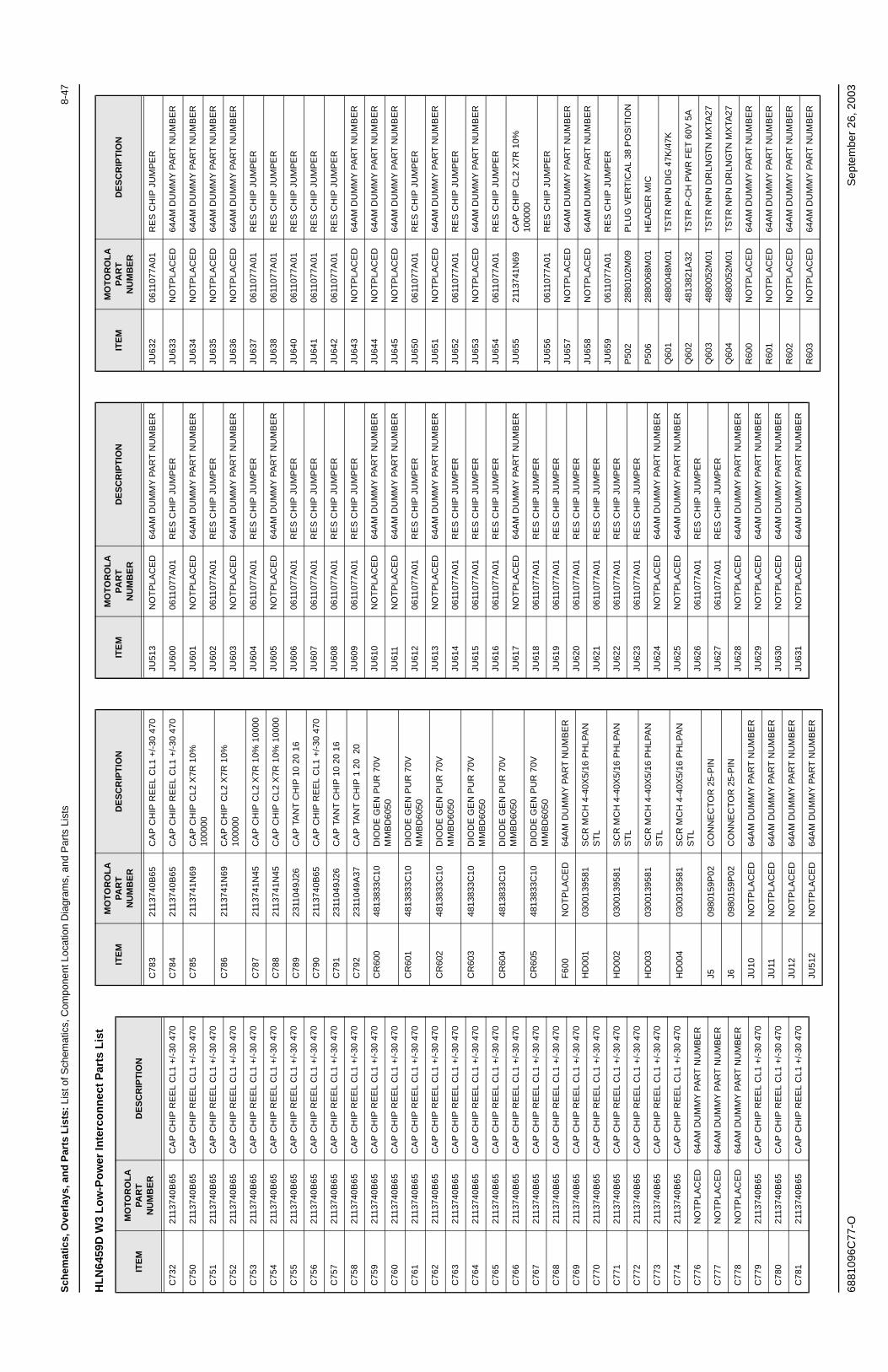
Sch
emat
ics,
Ove
rlay
s, a
nd
Par
ts L
ists
: Li
st o
f Sch
emat
ics,
Com
pone
nt L
ocat
ion
Dia
gram
s, a
nd P
arts
Lis
ts8-
47
6881
096C
77-O
Sep
tem
ber
26, 2
003
HL
N64
59D
W3
Lo
w-P
ow
er In
terc
on
nec
t P
arts
Lis
t
ITE
MM
OTO
RO
LA
PA
RT
N
UM
BE
RD
ES
CR
IPT
ION
C73
221
1374
0B65
CA
P C
HIP
RE
EL
CL1
+/-
30 4
70
C75
021
1374
0B65
CA
P C
HIP
RE
EL
CL1
+/-
30 4
70
C75
121
1374
0B65
CA
P C
HIP
RE
EL
CL1
+/-
30 4
70
C75
221
1374
0B65
CA
P C
HIP
RE
EL
CL1
+/-
30 4
70
C75
321
1374
0B65
CA
P C
HIP
RE
EL
CL1
+/-
30 4
70
C75
421
1374
0B65
CA
P C
HIP
RE
EL
CL1
+/-
30 4
70
C75
521
1374
0B65
CA
P C
HIP
RE
EL
CL1
+/-
30 4
70
C75
621
1374
0B65
CA
P C
HIP
RE
EL
CL1
+/-
30 4
70
C75
721
1374
0B65
CA
P C
HIP
RE
EL
CL1
+/-
30 4
70
C75
821
1374
0B65
CA
P C
HIP
RE
EL
CL1
+/-
30 4
70
C75
921
1374
0B65
CA
P C
HIP
RE
EL
CL1
+/-
30 4
70
C76
021
1374
0B65
CA
P C
HIP
RE
EL
CL1
+/-
30 4
70
C76
121
1374
0B65
CA
P C
HIP
RE
EL
CL1
+/-
30 4
70
C76
221
1374
0B65
CA
P C
HIP
RE
EL
CL1
+/-
30 4
70
C76
321
1374
0B65
CA
P C
HIP
RE
EL
CL1
+/-
30 4
70
C76
421
1374
0B65
CA
P C
HIP
RE
EL
CL1
+/-
30 4
70
C76
521
1374
0B65
CA
P C
HIP
RE
EL
CL1
+/-
30 4
70
C76
621
1374
0B65
CA
P C
HIP
RE
EL
CL1
+/-
30 4
70
C76
721
1374
0B65
CA
P C
HIP
RE
EL
CL1
+/-
30 4
70
C76
821
1374
0B65
CA
P C
HIP
RE
EL
CL1
+/-
30 4
70
C76
921
1374
0B65
CA
P C
HIP
RE
EL
CL1
+/-
30 4
70
C77
021
1374
0B65
CA
P C
HIP
RE
EL
CL1
+/-
30 4
70
C77
121
1374
0B65
CA
P C
HIP
RE
EL
CL1
+/-
30 4
70
C77
221
1374
0B65
CA
P C
HIP
RE
EL
CL1
+/-
30 4
70
C77
321
1374
0B65
CA
P C
HIP
RE
EL
CL1
+/-
30 4
70
C77
421
1374
0B65
CA
P C
HIP
RE
EL
CL1
+/-
30 4
70
C77
6N
OT
PLA
CE
D64
AM
DU
MM
Y P
AR
T N
UM
BE
R
C77
7N
OT
PLA
CE
D64
AM
DU
MM
Y P
AR
T N
UM
BE
R
C77
8N
OT
PLA
CE
D64
AM
DU
MM
Y P
AR
T N
UM
BE
R
C77
921
1374
0B65
CA
P C
HIP
RE
EL
CL1
+/-
30 4
70
C78
021
1374
0B65
CA
P C
HIP
RE
EL
CL1
+/-
30 4
70
C78
121
1374
0B65
CA
P C
HIP
RE
EL
CL1
+/-
30 4
70
C78
321
1374
0B65
CA
P C
HIP
RE
EL
CL1
+/-
30 4
70
C78
421
1374
0B65
CA
P C
HIP
RE
EL
CL1
+/-
30 4
70
C78
521
1374
1N69
CA
P C
HIP
CL2
X7R
10%
10
0000
C78
621
1374
1N69
CA
P C
HIP
CL2
X7R
10%
10
0000
C78
721
1374
1N45
CA
P C
HIP
CL2
X7R
10%
100
00
C78
821
1374
1N45
CA
P C
HIP
CL2
X7R
10%
100
00
C78
923
1104
9J26
CA
P T
AN
T C
HIP
10
20 1
6
C79
021
1374
0B65
CA
P C
HIP
RE
EL
CL1
+/-
30 4
70
C79
123
1104
9J26
CA
P T
AN
T C
HIP
10
20 1
6
C79
223
1104
9A37
CA
P T
AN
T C
HIP
1 2
0 2
0
CR
600
4813
833C
10D
IOD
E G
EN
PU
R 7
0V
MM
BD
6050
CR
601
4813
833C
10D
IOD
E G
EN
PU
R 7
0V
MM
BD
6050
CR
602
4813
833C
10D
IOD
E G
EN
PU
R 7
0V
MM
BD
6050
CR
603
4813
833C
10D
IOD
E G
EN
PU
R 7
0V
MM
BD
6050
CR
604
4813
833C
10D
IOD
E G
EN
PU
R 7
0V
MM
BD
6050
CR
605
4813
833C
10D
IOD
E G
EN
PU
R 7
0V
MM
BD
6050
F60
0N
OT
PLA
CE
D64
AM
DU
MM
Y P
AR
T N
UM
BE
R
HD
001
0300
1395
81S
CR
MC
H 4
-40X
5/16
PH
LPA
N
ST
L
HD
002
0300
1395
81S
CR
MC
H 4
-40X
5/16
PH
LPA
N
ST
L
HD
003
0300
1395
81S
CR
MC
H 4
-40X
5/16
PH
LPA
N
ST
L
HD
004
0300
1395
81S
CR
MC
H 4
-40X
5/16
PH
LPA
N
ST
L
J509
8015
9P02
CO
NN
EC
TO
R 2
5-P
IN
J609
8015
9P02
CO
NN
EC
TO
R 2
5-P
IN
JU10
NO
TP
LAC
ED
64A
M D
UM
MY
PA
RT
NU
MB
ER
JU11
NO
TP
LAC
ED
64A
M D
UM
MY
PA
RT
NU
MB
ER
JU12
NO
TP
LAC
ED
64A
M D
UM
MY
PA
RT
NU
MB
ER
JU51
2N
OT
PLA
CE
D64
AM
DU
MM
Y P
AR
T N
UM
BE
R
ITE
MM
OT
OR
OL
A
PAR
T
NU
MB
ER
DE
SC
RIP
TIO
N
JU51
3N
OT
PLA
CE
D64
AM
DU
MM
Y P
AR
T N
UM
BE
R
JU60
006
1107
7A01
RE
S C
HIP
JU
MP
ER
JU60
1N
OT
PLA
CE
D64
AM
DU
MM
Y P
AR
T N
UM
BE
R
JU60
206
1107
7A01
RE
S C
HIP
JU
MP
ER
JU60
3N
OT
PLA
CE
D64
AM
DU
MM
Y P
AR
T N
UM
BE
R
JU60
406
1107
7A01
RE
S C
HIP
JU
MP
ER
JU60
5N
OT
PLA
CE
D64
AM
DU
MM
Y P
AR
T N
UM
BE
R
JU60
606
1107
7A01
RE
S C
HIP
JU
MP
ER
JU60
706
1107
7A01
RE
S C
HIP
JU
MP
ER
JU60
806
1107
7A01
RE
S C
HIP
JU
MP
ER
JU60
906
1107
7A01
RE
S C
HIP
JU
MP
ER
JU61
0N
OT
PLA
CE
D64
AM
DU
MM
Y P
AR
T N
UM
BE
R
JU61
1N
OT
PLA
CE
D64
AM
DU
MM
Y P
AR
T N
UM
BE
R
JU61
206
1107
7A01
RE
S C
HIP
JU
MP
ER
JU61
3N
OT
PLA
CE
D64
AM
DU
MM
Y P
AR
T N
UM
BE
R
JU61
406
1107
7A01
RE
S C
HIP
JU
MP
ER
JU61
506
1107
7A01
RE
S C
HIP
JU
MP
ER
JU61
606
1107
7A01
RE
S C
HIP
JU
MP
ER
JU61
7N
OT
PLA
CE
D64
AM
DU
MM
Y P
AR
T N
UM
BE
R
JU61
806
1107
7A01
RE
S C
HIP
JU
MP
ER
JU61
906
1107
7A01
RE
S C
HIP
JU
MP
ER
JU62
006
1107
7A01
RE
S C
HIP
JU
MP
ER
JU62
106
1107
7A01
RE
S C
HIP
JU
MP
ER
JU62
206
1107
7A01
RE
S C
HIP
JU
MP
ER
JU62
306
1107
7A01
RE
S C
HIP
JU
MP
ER
JU62
4N
OT
PLA
CE
D64
AM
DU
MM
Y P
AR
T N
UM
BE
R
JU62
5N
OT
PLA
CE
D64
AM
DU
MM
Y P
AR
T N
UM
BE
R
JU62
606
1107
7A01
RE
S C
HIP
JU
MP
ER
JU62
706
1107
7A01
RE
S C
HIP
JU
MP
ER
JU62
8N
OT
PLA
CE
D64
AM
DU
MM
Y P
AR
T N
UM
BE
R
JU62
9N
OT
PLA
CE
D64
AM
DU
MM
Y P
AR
T N
UM
BE
R
JU63
0N
OT
PLA
CE
D64
AM
DU
MM
Y P
AR
T N
UM
BE
R
JU63
1N
OT
PLA
CE
D64
AM
DU
MM
Y P
AR
T N
UM
BE
R
ITE
MM
OT
OR
OL
A
PA
RT
N
UM
BE
RD
ES
CR
IPT
ION
JU63
206
1107
7A01
RE
S C
HIP
JU
MP
ER
JU63
3N
OT
PLA
CE
D64
AM
DU
MM
Y P
AR
T N
UM
BE
R
JU63
4N
OT
PLA
CE
D64
AM
DU
MM
Y P
AR
T N
UM
BE
R
JU63
5N
OT
PLA
CE
D64
AM
DU
MM
Y P
AR
T N
UM
BE
R
JU63
6N
OT
PLA
CE
D64
AM
DU
MM
Y P
AR
T N
UM
BE
R
JU63
706
1107
7A01
RE
S C
HIP
JU
MP
ER
JU63
806
1107
7A01
RE
S C
HIP
JU
MP
ER
JU64
006
1107
7A01
RE
S C
HIP
JU
MP
ER
JU64
106
1107
7A01
RE
S C
HIP
JU
MP
ER
JU64
206
1107
7A01
RE
S C
HIP
JU
MP
ER
JU64
3N
OT
PLA
CE
D64
AM
DU
MM
Y P
AR
T N
UM
BE
R
JU64
4N
OT
PLA
CE
D64
AM
DU
MM
Y P
AR
T N
UM
BE
R
JU64
5N
OT
PLA
CE
D64
AM
DU
MM
Y P
AR
T N
UM
BE
R
JU65
006
1107
7A01
RE
S C
HIP
JU
MP
ER
JU65
1N
OT
PLA
CE
D64
AM
DU
MM
Y P
AR
T N
UM
BE
R
JU65
206
1107
7A01
RE
S C
HIP
JU
MP
ER
JU65
3N
OT
PLA
CE
D64
AM
DU
MM
Y P
AR
T N
UM
BE
R
JU65
406
1107
7A01
RE
S C
HIP
JU
MP
ER
JU65
521
1374
1N69
CA
P C
HIP
CL2
X7R
10%
10
0000
JU65
606
1107
7A01
RE
S C
HIP
JU
MP
ER
JU65
7N
OT
PLA
CE
D64
AM
DU
MM
Y P
AR
T N
UM
BE
R
JU65
8N
OT
PLA
CE
D64
AM
DU
MM
Y P
AR
T N
UM
BE
R
JU65
906
1107
7A01
RE
S C
HIP
JU
MP
ER
P50
228
8010
2M09
PLU
G V
ER
TIC
AL
38 P
OS
ITIO
N
P50
628
8006
8M01
HE
AD
ER
MIC
Q60
148
8004
8M01
TS
TR
NP
N D
IG 4
7K/4
7K
Q60
248
1382
1A32
TS
TR
P-C
H P
WR
FE
T 6
0V 5
A
Q60
348
8005
2M01
TS
TR
NP
N D
RLN
GT
N M
XTA
27
Q60
448
8005
2M01
TS
TR
NP
N D
RLN
GT
N M
XTA
27
R60
0N
OT
PLA
CE
D64
AM
DU
MM
Y P
AR
T N
UM
BE
R
R60
1N
OT
PLA
CE
D64
AM
DU
MM
Y P
AR
T N
UM
BE
R
R60
2N
OT
PLA
CE
D64
AM
DU
MM
Y P
AR
T N
UM
BE
R
R60
3N
OT
PLA
CE
D64
AM
DU
MM
Y P
AR
T N
UM
BE
R
ITE
MM
OTO
RO
LA
P
AR
T
NU
MB
ER
DE
SC
RIP
TIO
N

8-48
Sch
emat
ics,
Ove
rlay
s, a
nd
Par
ts L
ists
: Li
st o
f Sch
emat
ics,
Com
pone
nt L
ocat
ion
Dia
gram
s, a
nd P
arts
Lis
ts
Sep
tem
ber
26, 2
003
6881
096C
77-O
R60
4N
OT
PLA
CE
D64
AM
DU
MM
Y P
AR
T N
UM
BE
R
R60
5N
OT
PLA
CE
D64
AM
DU
MM
Y P
AR
T N
UM
BE
R
R60
6N
OT
PLA
CE
D64
AM
DU
MM
Y P
AR
T N
UM
BE
R
R60
7N
OT
PLA
CE
D64
AM
DU
MM
Y P
AR
T N
UM
BE
R
R60
806
1107
7A01
RE
S C
HIP
JU
MP
ER
R60
906
1107
7B15
RE
S C
HIP
47K
5 1
/8W
R61
006
1107
7B15
RE
S C
HIP
47K
5 1
/8W
R61
206
1107
7B23
RE
S C
HIP
100
K 5
1/8
W
R61
306
1107
7B15
RE
S C
HIP
47K
5 1
/8W
R61
406
1107
7A98
RE
S C
HIP
10K
5 1
/8W
R61
506
1107
7A98
RE
S C
HIP
10K
5 1
/8W
R61
606
1107
7A98
RE
S C
HIP
10K
5 1
/8W
R61
706
1107
7A98
RE
S C
HIP
10K
5 1
/8W
R61
806
1107
7A96
RE
S C
HIP
820
0 5
1/8
R61
906
1107
7B15
RE
S C
HIP
47K
5 1
/8W
R62
006
1107
7A54
RE
S C
HIP
150
5 1
/8W
R62
106
1107
7A74
RE
S C
HIP
100
0 5
1/8
R62
206
1107
7A74
RE
S C
HIP
100
0 5
1/8
R62
306
1107
7A74
RE
S C
HIP
100
0 5
1/8
U60
0N
OT
PLA
CE
D64
AM
DU
MM
Y P
AR
T N
UM
BE
R
U60
151
1380
6A05
IC F
LIP
-FLO
P,D
UA
L D
U60
251
1380
6A37
IC S
CH
MIT
T T
RIG
GE
R,H
EX
U60
351
1381
6A19
IC A
DJ
LO D
RO
PO
UT
PO
S
RE
G .8
A
VR
600
4813
830A
28D
IOD
E 1
5V 5
% 2
25M
W
MM
BZ
5245
B_
VR
601
4813
830A
28D
IOD
E 1
5V 5
% 2
25M
W
MM
BZ
5245
B_
VR
602
4813
830A
28D
IOD
E 1
5V 5
% 2
25M
W
MM
BZ
5245
B_
VR
603
4813
830A
28D
IOD
E 1
5V 5
% 2
25M
W
MM
BZ
5245
B_
VR
604
4813
830A
28D
IOD
E 1
5V 5
% 2
25M
W
MM
BZ
5245
B_
VR
605
4813
830A
28D
IOD
E 1
5V 5
% 2
25M
W
MM
BZ
5245
B_
ITE
MM
OT
OR
OL
A
PA
RT
N
UM
BE
RD
ES
CR
IPT
ION
VR
606
4813
830A
28D
IOD
E 1
5V 5
% 2
25M
W
MM
BZ
5245
B_
VR
607
4813
830A
28D
IOD
E 1
5V 5
% 2
25M
W
MM
BZ
5245
B_
VR
608
4813
830A
28D
IOD
E 1
5V 5
% 2
25M
W
MM
BZ
5245
B_
VR
609
4813
830A
28D
IOD
E 1
5V 5
% 2
25M
W
MM
BZ
5245
B_
VR
610
4813
830A
28D
IOD
E 1
5V 5
% 2
25M
W
MM
BZ
5245
B_
VR
611
4813
830A
28D
IOD
E 1
5V 5
% 2
25M
W
MM
BZ
5245
B_
VR
612
4813
830A
28D
IOD
E 1
5V 5
% 2
25M
W
MM
BZ
5245
B_
VR
613
4813
830A
28D
IOD
E 1
5V 5
% 2
25M
W
MM
BZ
5245
B_
VR
614
4813
832C
28Z
EN
ER
BP
LR 1
5V F
OR
ES
D
SO
T23
VR
615
4813
832C
28Z
EN
ER
BP
LR 1
5V F
OR
ES
D
SO
T23
VR
616
4813
832C
28Z
EN
ER
BP
LR 1
5V F
OR
ES
D
SO
T23
VR
617
4813
832C
28Z
EN
ER
BP
LR 1
5V F
OR
ES
D
SO
T23
VR
618
4813
830A
28D
IOD
E 1
5V 5
% 2
25M
W
MM
BZ
5245
B_
VR
619
4813
830A
28D
IOD
E 1
5V 5
% 2
25M
W
MM
BZ
5245
B_
VR
620
4813
830A
28D
IOD
E 1
5V 5
% 2
25M
W
MM
BZ
5245
B_
VR
621
4813
830A
28D
IOD
E 1
5V 5
% 2
25M
W
MM
BZ
5245
B_
VR
622
4813
830A
28D
IOD
E 1
5V 5
% 2
25M
W
MM
BZ
5245
B_
VR
623
4813
830A
28D
IOD
E 1
5V 5
% 2
25M
W
MM
BZ
5245
B_
VR
624
4813
830A
28D
IOD
E 1
5V 5
% 2
25M
W
MM
BZ
5245
B_
VR
625
4880
140L
23D
IOD
E S
OT
ZE
NE
R 1
8V
TAP
E&
RE
EL
VR
626
4813
830A
28D
IOD
E 1
5V 5
% 2
25M
W
MM
BZ
5245
B_
VR
627
NO
TP
LAC
ED
64A
M D
UM
MY
PA
RT
NU
MB
ER
ITE
MM
OTO
RO
LA
P
AR
T
NU
MB
ER
DE
SC
RIP
TIO
N

Sch
emat
ics,
Ove
rlay
s, a
nd
Par
ts L
ists
: Li
st o
f Sch
emat
ics,
Com
pone
nt L
ocat
ion
Dia
gram
s, a
nd P
arts
Lis
ts8-
49
6881
096C
77-O
Sep
tem
ber
26, 2
003
HL
N63
65E
Mo
torc
ycle
Inte
rco
nn
ect
Par
ts L
ist
ITE
MM
OTO
RO
LA
PA
RT
N
UM
BE
RD
ES
CR
IPT
ION
C75
421
1374
0B65
CA
P C
HIP
RE
EL
CL1
+/-
30 4
70
C75
521
1374
0B65
CA
P C
HIP
RE
EL
CL1
+/-
30 4
70
C77
221
1374
1N45
CA
P C
HIP
CL2
X7R
10%
100
00
C77
321
1374
1N45
CA
P C
HIP
CL2
X7R
10%
100
00
GS
142
0574
7Z01
CLI
P G
RN
D
GS
242
0574
7Z01
CLI
P G
RN
D
J509
8015
9P02
CO
NN
EC
TO
R 2
5-P
IN
JU12
0611
077A
01R
ES
CH
IP J
UM
PE
R
JU51
206
1107
7A01
RE
S C
HIP
JU
MP
ER
JU51
306
1107
7A01
RE
S C
HIP
JU
MP
ER
JU60
006
1107
7A01
RE
S C
HIP
JU
MP
ER
JU60
106
1107
7A01
RE
S C
HIP
JU
MP
ER
JU60
306
1107
7A01
RE
S C
HIP
JU
MP
ER
JU60
406
1107
7A01
RE
S C
HIP
JU
MP
ER
JU60
606
1107
7A01
RE
S C
HIP
JU
MP
ER
JU60
706
1107
7A01
RE
S C
HIP
JU
MP
ER
JU60
806
1107
7A01
RE
S C
HIP
JU
MP
ER
JU60
906
1107
7A01
RE
S C
HIP
JU
MP
ER
JU61
206
1107
7A01
RE
S C
HIP
JU
MP
ER
JU61
306
1107
7A01
RE
S C
HIP
JU
MP
ER
JU61
906
1107
7A01
RE
S C
HIP
JU
MP
ER
JU62
006
1107
7A01
RE
S C
HIP
JU
MP
ER
JU62
106
1107
7A01
RE
S C
HIP
JU
MP
ER
JU62
206
1107
7A01
RE
S C
HIP
JU
MP
ER
JU62
306
1107
7A01
RE
S C
HIP
JU
MP
ER
JU63
106
1107
7A01
RE
S C
HIP
JU
MP
ER
JU63
206
1107
7A01
RE
S C
HIP
JU
MP
ER
JU63
706
1107
7A01
RE
S C
HIP
JU
MP
ER
JU63
806
1107
7A01
RE
S C
HIP
JU
MP
ER
JU64
006
1107
7A01
RE
S C
HIP
JU
MP
ER
JU64
106
1107
7A01
RE
S C
HIP
JU
MP
ER
JU64
206
1107
7A01
RE
S C
HIP
JU
MP
ER
JU65
106
1107
7A01
RE
S C
HIP
JU
MP
ER
JU65
406
1107
7A01
RE
S C
HIP
JU
MP
ER
JU65
606
1107
7A01
RE
S C
HIP
JU
MP
ER
JU65
706
1107
7A01
RE
S C
HIP
JU
MP
ER
JU65
906
1107
7A01
RE
S C
HIP
JU
MP
ER
P50
228
8010
2M09
PLU
G V
ER
TIC
AL
38 P
OS
ITIO
N
P50
628
8006
8M01
HE
AD
ER
MIC
R60
806
1107
7A74
RE
S C
HIP
100
0 5
1/8
R61
806
1107
7A96
RE
S C
HIP
820
0 5
1/8
VR
600
4813
830A
28D
IOD
E 1
5V 5
% 2
25M
W
MM
BZ
5245
B_
VR
601
4813
830A
28D
IOD
E 1
5V 5
% 2
25M
W
MM
BZ
5245
B_
VR
602
4813
830A
28D
IOD
E 1
5V 5
% 2
25M
W
MM
BZ
5245
B_
VR
603
4813
830A
28D
IOD
E 1
5V 5
% 2
25M
W
MM
BZ
5245
B_
VR
604
4813
830A
28D
IOD
E 1
5V 5
% 2
25M
W
MM
BZ
5245
B_
VR
605
4813
830A
28D
IOD
E 1
5V 5
% 2
25M
W
MM
BZ
5245
B_
VR
606
4813
830A
28D
IOD
E 1
5V 5
% 2
25M
W
MM
BZ
5245
B_
VR
607
4813
830A
28D
IOD
E 1
5V 5
% 2
25M
W
MM
BZ
5245
B_
VR
608
4813
830A
28D
IOD
E 1
5V 5
% 2
25M
W
MM
BZ
5245
B_
VR
609
4813
830A
28D
IOD
E 1
5V 5
% 2
25M
W
MM
BZ
5245
B_
VR
610
4813
830A
28D
IOD
E 1
5V 5
% 2
25M
W
MM
BZ
5245
B_
VR
611
4813
830A
28D
IOD
E 1
5V 5
% 2
25M
W
MM
BZ
5245
B_
VR
612
4813
830A
28D
IOD
E 1
5V 5
% 2
25M
W
MM
BZ
5245
B_
VR
613
4813
830A
28D
IOD
E 1
5V 5
% 2
25M
W
MM
BZ
5245
B_
VR
618
4813
830A
28D
IOD
E 1
5V 5
% 2
25M
W
MM
BZ
5245
B_
ITE
MM
OT
OR
OL
A
PAR
T
NU
MB
ER
DE
SC
RIP
TIO
N
VR
619
4813
830A
28D
IOD
E 1
5V 5
% 2
25M
W
MM
BZ
5245
B_
VR
620
4813
830A
28D
IOD
E 1
5V 5
% 2
25M
W
MM
BZ
5245
B_
VR
621
4813
830A
28D
IOD
E 1
5V 5
% 2
25M
W
MM
BZ
5245
B_
VR
622
4813
830A
28D
IOD
E 1
5V 5
% 2
25M
W
MM
BZ
5245
B_
ITE
MM
OT
OR
OL
A
PA
RT
N
UM
BE
RD
ES
CR
IPT
ION
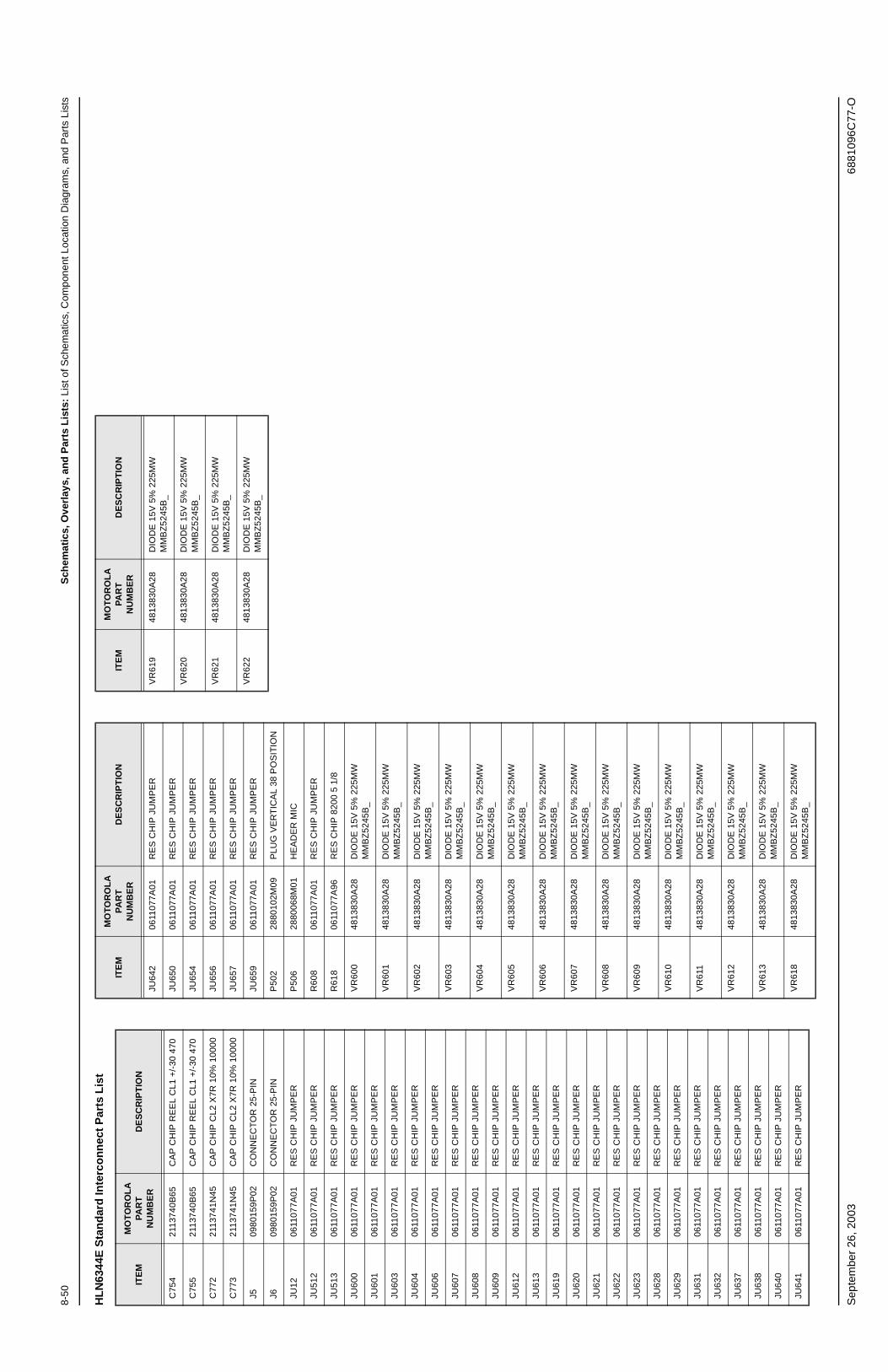
8-50
Sch
emat
ics,
Ove
rlay
s, a
nd
Par
ts L
ists
: Li
st o
f Sch
emat
ics,
Com
pone
nt L
ocat
ion
Dia
gram
s, a
nd P
arts
Lis
ts
Sep
tem
ber
26, 2
003
6881
096C
77-O
HL
N63
44E
Sta
nd
ard
Inte
rco
nn
ect
Par
ts L
ist
ITE
MM
OT
OR
OL
A
PA
RT
N
UM
BE
RD
ES
CR
IPT
ION
C75
421
1374
0B65
CA
P C
HIP
RE
EL
CL1
+/-
30 4
70
C75
521
1374
0B65
CA
P C
HIP
RE
EL
CL1
+/-
30 4
70
C77
221
1374
1N45
CA
P C
HIP
CL2
X7R
10%
100
00
C77
321
1374
1N45
CA
P C
HIP
CL2
X7R
10%
100
00
J509
8015
9P02
CO
NN
EC
TO
R 2
5-P
IN
J609
8015
9P02
CO
NN
EC
TO
R 2
5-P
IN
JU12
0611
077A
01R
ES
CH
IP J
UM
PE
R
JU51
206
1107
7A01
RE
S C
HIP
JU
MP
ER
JU51
306
1107
7A01
RE
S C
HIP
JU
MP
ER
JU60
006
1107
7A01
RE
S C
HIP
JU
MP
ER
JU60
106
1107
7A01
RE
S C
HIP
JU
MP
ER
JU60
306
1107
7A01
RE
S C
HIP
JU
MP
ER
JU60
406
1107
7A01
RE
S C
HIP
JU
MP
ER
JU60
606
1107
7A01
RE
S C
HIP
JU
MP
ER
JU60
706
1107
7A01
RE
S C
HIP
JU
MP
ER
JU60
806
1107
7A01
RE
S C
HIP
JU
MP
ER
JU60
906
1107
7A01
RE
S C
HIP
JU
MP
ER
JU61
206
1107
7A01
RE
S C
HIP
JU
MP
ER
JU61
306
1107
7A01
RE
S C
HIP
JU
MP
ER
JU61
906
1107
7A01
RE
S C
HIP
JU
MP
ER
JU62
006
1107
7A01
RE
S C
HIP
JU
MP
ER
JU62
106
1107
7A01
RE
S C
HIP
JU
MP
ER
JU62
206
1107
7A01
RE
S C
HIP
JU
MP
ER
JU62
306
1107
7A01
RE
S C
HIP
JU
MP
ER
JU62
806
1107
7A01
RE
S C
HIP
JU
MP
ER
JU62
906
1107
7A01
RE
S C
HIP
JU
MP
ER
JU63
106
1107
7A01
RE
S C
HIP
JU
MP
ER
JU63
206
1107
7A01
RE
S C
HIP
JU
MP
ER
JU63
706
1107
7A01
RE
S C
HIP
JU
MP
ER
JU63
806
1107
7A01
RE
S C
HIP
JU
MP
ER
JU64
006
1107
7A01
RE
S C
HIP
JU
MP
ER
JU64
106
1107
7A01
RE
S C
HIP
JU
MP
ER
JU64
206
1107
7A01
RE
S C
HIP
JU
MP
ER
JU65
006
1107
7A01
RE
S C
HIP
JU
MP
ER
JU65
406
1107
7A01
RE
S C
HIP
JU
MP
ER
JU65
606
1107
7A01
RE
S C
HIP
JU
MP
ER
JU65
706
1107
7A01
RE
S C
HIP
JU
MP
ER
JU65
906
1107
7A01
RE
S C
HIP
JU
MP
ER
P50
228
8010
2M09
PLU
G V
ER
TIC
AL
38 P
OS
ITIO
N
P50
628
8006
8M01
HE
AD
ER
MIC
R60
806
1107
7A01
RE
S C
HIP
JU
MP
ER
R61
806
1107
7A96
RE
S C
HIP
820
0 5
1/8
VR
600
4813
830A
28D
IOD
E 1
5V 5
% 2
25M
W
MM
BZ
5245
B_
VR
601
4813
830A
28D
IOD
E 1
5V 5
% 2
25M
W
MM
BZ
5245
B_
VR
602
4813
830A
28D
IOD
E 1
5V 5
% 2
25M
W
MM
BZ
5245
B_
VR
603
4813
830A
28D
IOD
E 1
5V 5
% 2
25M
W
MM
BZ
5245
B_
VR
604
4813
830A
28D
IOD
E 1
5V 5
% 2
25M
W
MM
BZ
5245
B_
VR
605
4813
830A
28D
IOD
E 1
5V 5
% 2
25M
W
MM
BZ
5245
B_
VR
606
4813
830A
28D
IOD
E 1
5V 5
% 2
25M
W
MM
BZ
5245
B_
VR
607
4813
830A
28D
IOD
E 1
5V 5
% 2
25M
W
MM
BZ
5245
B_
VR
608
4813
830A
28D
IOD
E 1
5V 5
% 2
25M
W
MM
BZ
5245
B_
VR
609
4813
830A
28D
IOD
E 1
5V 5
% 2
25M
W
MM
BZ
5245
B_
VR
610
4813
830A
28D
IOD
E 1
5V 5
% 2
25M
W
MM
BZ
5245
B_
VR
611
4813
830A
28D
IOD
E 1
5V 5
% 2
25M
W
MM
BZ
5245
B_
VR
612
4813
830A
28D
IOD
E 1
5V 5
% 2
25M
W
MM
BZ
5245
B_
VR
613
4813
830A
28D
IOD
E 1
5V 5
% 2
25M
W
MM
BZ
5245
B_
VR
618
4813
830A
28D
IOD
E 1
5V 5
% 2
25M
W
MM
BZ
5245
B_
ITE
MM
OTO
RO
LA
P
AR
T
NU
MB
ER
DE
SC
RIP
TIO
N
VR
619
4813
830A
28D
IOD
E 1
5V 5
% 2
25M
W
MM
BZ
5245
B_
VR
620
4813
830A
28D
IOD
E 1
5V 5
% 2
25M
W
MM
BZ
5245
B_
VR
621
4813
830A
28D
IOD
E 1
5V 5
% 2
25M
W
MM
BZ
5245
B_
VR
622
4813
830A
28D
IOD
E 1
5V 5
% 2
25M
W
MM
BZ
5245
B_
ITE
MM
OTO
RO
LA
PA
RT
N
UM
BE
RD
ES
CR
IPT
ION

Sch
emat
ics,
Ove
rlay
s, a
nd
Par
ts L
ists
: Li
st o
f Sch
emat
ics,
Com
pone
nt L
ocat
ion
Dia
gram
s, a
nd P
arts
Lis
ts8-
51
6881
096C
77-O
Sep
tem
ber
26, 2
003
Fig
ure
8-30
. HM
N10
80A
, HM
N10
61A
, HM
N10
79A
Mic
roph
one
Boa
rd O
verla
y
Fig
ure
8-31
. HM
N10
80A
, HM
N10
61A
, HM
N10
79A
Mic
roph
one
Sch
emat
icic
++
GR
NBL
K
R13
06C
1307
C13
08
Q13
02
C1306
R1303
C1302
C1301
R1305
C1305
R13
02 C13
09
C13
04
CR
1301
MK1
301
S130
1
BLU
WH
TR
ED
MAE
PF-2
7698
-O
VR13
0112
VS1
301
PUSH
TO
TAL
KC
1308
0.27
C13
0410
C13
020.
001
C13
0127
pF
MK1
301
C13
070.
001
R13
0656
R13
022.
2KR
1303
1K
R13
0510
0K C13
0636
pF
C13
050.
22
Q13
02M
8208
C13
0962
pF
(VEH
ICLE
CH
ASSI
SG
RO
UN
D)
MIC
HAN
G-U
PC
LIP
MIC
HAN
G-U
PST
UD
H.U
.B. (
BLU
)
MIC
HI (
RED
)
PTT
(GR
N)
DIG
GN
D (W
HT)
MIC
LO
(BLK
)
MIC
RO
PHO
NE
CO
NN
ECTO
R J
104
(DET
AIL
SHO
WN
FRO
M C
ON
NEC
TOR
FRO
NT
VIEW
)
N.C
.
+
MAE
PF-2
7699
-O
HM
N10
80A
, HM
N10
61A
, HM
N10
79A
Mic
rop
ho
ne
Par
ts L
ist
ITE
MM
OT
OR
OL
APA
RT
NU
MB
ER
DE
SC
RIP
TIO
N
C13
0121
1103
8H35
CA
P 2
7pF
50V
C13
02,
C13
0721
1103
9B13
CA
P 1
000
50V
C13
0423
1104
8C10
CA
P 1
0 50
V
C13
0508
1105
1A15
0811
051A
11C
AP
.22
63V
(H
MN
1080
A &
HM
N10
79A
onl
y)C
AP
.047
63V
(H
MN
1061
A o
nly)
C13
0621
8213
3G39
2111
038P
50C
AP
36
500V
(H
MN
1080
A &
HM
N10
79A
onl
y)C
AP
220
50V
(H
MN
1061
A o
nly)
C13
0823
8239
7D25
0811
051A
14C
AP
.27p
F 2
0V (
HM
N10
80A
& H
MN
1079
A o
nly)
CA
P .1
5 63
V (
HM
N10
61A
onl
y)
C13
0921
1101
4H44
CA
P 6
2pF
100
V
CR
1301
4811
034A
3612
V Z
ener
MK
1301
5080
258E
06E
LEC
TR
ET
MIC
CT
RG
Q13
0248
1104
3C05
NP
N
R13
0206
1100
9C57
RE
S 2
200
1/4
R13
0306
1100
9C49
RE
S 1
000
1/4
R13
0506
1100
9C97
RE
S 1
00K
1/4
R13
0606
1100
9C19
RE
S 5
6 5
1/4
S13
0140
8006
5E02
SW
MO
ME
NTA
RY

8-52
Sch
emat
ics,
Ove
rlay
s, a
nd
Par
ts L
ists
: Li
st o
f Sch
emat
ics,
Com
pone
nt L
ocat
ion
Dia
gram
s, a
nd P
arts
Lis
ts
Sep
tem
ber
26, 2
003
6881
096C
77-O
No
tes

Appendix A Replacement Parts Ordering
A.1 Basic Ordering InformationWhen ordering replacement parts or equipment information, the complete identification number should be included. This applies to all components, kits, and chassis. If the component part number is not known, the order should include the number of the chassis or kit of which it is a part, and sufficient description of the desired component to identify it.
Crystal orders should specify the crystal type number, crystal and carrier frequency, and the model number in which the part is used.
The ASTRO Digital Spectra/Digital Spectra Plus Mobile Radios Control Head Manual (Motorola publication part number 6881096C77) includes complete parts lists and parts numbers.
A.2 Motorola OnlineMotorola Online users can access our online catalog at
https://www.motorola.com/businessonline
To register for online access:
• Domestic customers: please call 800-814-0601 (U.S. and Canada).
• International customers: please go to https://www.motorola.com/businessonline and click on “Sign Up Now.”
A.3 Mail OrdersSend written orders to the following addresses:
*The Radio Products Services Division (RPSD) was formerly known as the Customer Care and Services Division (CCSD) and/or the Accessories and Aftermarket Division (AAD).
Replacement Parts/Test Equipment/Manuals/Crystal Service Items:
Motorola Inc.Radio Products Services Division*Attention: Order Processing2200 Galvin DriveElgin, IL 60123U.S.A.
Federal Government Orders:
Motorola Inc.U.S. Federal Government Markets DivisionAttention: Order Processing7230 Parkway DriveLandover, MD 21076U.S.A.
International Orders:
Motorola Inc.Radio Products Services Division*Attention: Order Processing2200 Galvin DriveElgin, IL 60123U.S.A.
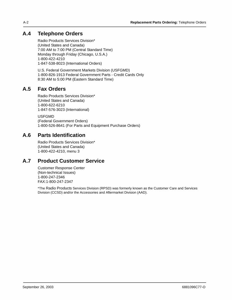
A-2 Replacement Parts Ordering: Telephone Orders
A.4 Telephone OrdersRadio Products Services Division*(United States and Canada)7:00 AM to 7:00 PM (Central Standard Time)Monday through Friday (Chicago, U.S.A.)1-800-422-42101-847-538-8023 (International Orders)
U.S. Federal Government Markets Division (USFGMD)1-800-826-1913 Federal Government Parts - Credit Cards Only8:30 AM to 5:00 PM (Eastern Standard Time)
A.5 Fax OrdersRadio Products Services Division*(United States and Canada)1-800-622-62101-847-576-3023 (International)
USFGMD(Federal Government Orders)1-800-526-8641 (For Parts and Equipment Purchase Orders)
A.6 Parts IdentificationRadio Products Services Division*(United States and Canada)1-800-422-4210, menu 3
A.7 Product Customer ServiceCustomer Response Center(Non-technical Issues)1-800-247-2346FAX:1-800-247-2347
*The Radio Products Services Division (RPSD) was formerly known as the Customer Care and Services Division (CCSD) and/or the Accessories and Aftermarket Division (AAD).
September 26, 2003 6881096C77-O

Index-1
Index Index
C
cable, P501 extender 6-4cautions 1-1charts, troubleshooting 5-12cleaning
circuit boards 2-1components 2-1external surfaces 2-1
component location diagrams 8-1control heads
cabling 6-4Model W3 1-2Models W4, W5, W7, W9 1-4overview 1-2replacing 5-7
Model W3 5-7Model W4, W5, W7 5-8Model W9 5-10
vehicle interface port (VIP) 3-12controls
Model W3 1-3Model W4, W5, W7, W9 1-6
copyrightscomputer software iidocument ii
E
extender cable, P501 6-4
H
handling precautions 2-2
J
jumper configurations 3-11
M
maintenancecleaning 2-1inspection 2-1
manualnotations 1-1revisions ii
Microphoneexploded view 7-6parts list 7-6
Model W3backlight circuit 3-3display circuit 3-1exploded view 7-2final reassembly 5-11jumper selection 3-3keypad side keys and top keys 3-2microphone preamplifier and PTT 3-2
On/0ff hook control 3-3operation 3-1parts list 7-2power On/Off 3-4power supply 3-3replacing the control head 5-7SB9600 Serial Bus Interface 3-1status LEDs 3-3
Model W9control board 3-9
bus transceiver 3-10EEPROM write-protect circuit 3-11ignition sense circuits 3-10microprocessor 3-9power supply 3-10vacuum fluorescent voltage converter 3-10vehicle interface ports 3-10watchdog timer 3-9
controls and indicators 3-9default jumper settings 3-11display 3-8display board 3-11
backlight LEDs 3-11status LEDs 3-11vacuum fluorescent display 3-11vacuum fluorescent display driver 3-11
exploded view 7-5operation 3-8parts list 7-5replacing the control head 5-10vehicle interface port (VIP) 3-14
Models W4, W5, W7backlight LEDs 3-8bus busy 3-6hang-up button (HUB) 3-7ignition sense circuitry 3-7interface circuitry 3-5keypad scan 3-7microcomputer 3-5Model W4 exploded view 7-3Model W4 parts list 7-3Models W5, W7 exploded view 7-4Models W5, W7 parts list 7-4operation 3-4power switch/ignition 3-4push-to-talk (PTT) 3-7replacing the control head 5-8replacing the remote back housing
interface board 5-5replacing the vacuum fluorescent display 5-5reset 3-6serial bus data 3-6vacuum fluorescent display 3-8vacuum fluorescent display driver IC 3-8vacuum fluorescent voltage converter circuitry 3-7vehicle interface port 3-12voltage regulator 3-5
N
notations 1-1
6881096C77-O September 26, 2003

Index-2
P
parts list 8-1large pushbutton parts 7-7Microphone 7-6Model W3 7-2Model W4 7-3Model W5 7-4Model W7 7-4Model W9 7-5small pushbutton parts 7-7
parts, ordering replacement A-1product safety information iiPTT (push-to-talk) 3-7
R
reassembly, final 5-11Model W3 5-11
remote back housing interface board, replacing 5-5remote interconnect board, replacing 5-6replacement parts, ordering A-1replacing
control head 5-7remote back housing interface board 5-5remote interconnect board 5-6vacuum fluorescent display 5-5
RF exposure compliance information ii
S
schematics 8-1Serial Bus Data 3-6
T
test equipment and service aids 4-1trademark information iitroubleshooting 5-1
charts 5-12final reassembly 5-11replacing the control head 5-7replacing the remote back housing
interface board 5-5replacing the remote interconnect board 5-6replacing the vacuum fluorescent display 5-5tools and supplies 5-1waveforms 5-2
V
vacuum fluorescent display, replacing 5-5vehicle interface port (VIP) 3-12
Model W4, W5, W7 3-12VIP input connections 3-13VIP output connections 3-12
Model W9 3-14VIP input connections 3-14VIP output connections 3-14
VIP output connectionsdash-mount installations 3-12remote-mount installations 3-13
W
warranty xiwaveforms
troubleshooting 5-2
September 26, 2003 6881096C77-O


6881096C77-O
*6881096C77*
MOTOROLA, the Stylized M Logo, ASTRO, and Spectra are
registered in the U.S. Patent and Trademark Office. All other
product or service names are the property of their respective owners.
© Motorola, Inc. 2003
All rights reserved. Printed in U.S.A.
Motorola, Inc.
8000 West Sunrise Boulevard
Ft. Lauderdale, FL 33322