VTT as an innovation partner in micro and nano · PDF fileVTT as an innovation partner in...
65
VTT as an innovation partner in micro and nano technogies Aarne Oja Director, High Performance Microsystems VTT Technical Research Centre of Finland 11 Feb 2010 [email protected]
Transcript of VTT as an innovation partner in micro and nano · PDF fileVTT as an innovation partner in...

VTT as an innovation partnerin micro and nano technogies
Aarne OjaDirector, High Performance MicrosystemsVTT Technical Research Centre of Finland11 Feb [email protected]

224/03/2010
Executive Summary
VTT, a leading European research intitute in microtechnology, isactively looking for new innovation partnersVTT has a number of product prototypes with a high businesspotential and a short time-to-marketUnlike most research institutes, VTT is open to external users andis actively looking for joint ventures to commercialize its technologyMarkets for VTT innovations in micro and nanotechnologies:industrial, automotive, and consumer-electronics senors, high-frequency passive components, LED lightning, opticaltelecommunication, medical

324/03/2010
Contents
Overview of VTTInternational R&D organization
VTT facilities in micro and nano technology: MicronovaMicrova as a technology park for companies
VTT Micronova as an industrial fabVTT spin-offsVTT products close to commercialization
Markets: industrial, automotive, and consumer-electronicssenors, high-frequency passive components, LED lightning,optical telecommunication, medical
Summary of collaboration possibilities

424/03/2010
VTT creates business from technology
We enhance the competitiveness of our customers through newtechnology and science-based innovations.
Our services cover all the important stages of the innovation processfrom technology and market foresight to commercialization.
We combine our top-level multidisciplinary expertise in novel ways tocreate globally new leading-edge technologies.

524/03/2010
VTT Group in brief
Personnel 2920Turnover 276 M€ (budget for 2010)
VTT’s operationsResearch and Development Strategic Research Business Solutions IP Business
Corporate Services
VTT’s companiesVTT Expert Services Ltd VTT Ventures Ltd VTT International Ltd
Focus areas of researchApplied materialsBio- and chemical processesEnergyInformation and communication technologiesIndustrial systems managementMicrotechnologies and electronicsTechnology in the communityBusiness research

624/03/2010
Income from the private domestic sector 30%Income from the public domestic sector 25%Income from abroad 15%Basic governmental funding 30%
Turnover by type of incomeTurnover 245 M€ in 2008

724/03/2010
Basicresearch
Development
VTT
INDUSTRY
UNIVERSITIES
Appliedresearch
VTT’s status as performer of R&D work

824/03/2010
VTT Group structure 2010
VTT Expert Services LtdSpecialist reports and assessmentsCertification and approval servicesTesting, inspection and calibration
VTT International LtdAdministration anddevelopment of internationalservice points
VTT Ventures LtdOwnership and developmentof spin-offs
Strategic researchSelf-financed researchJointly funded research
Group ServicesSupport functions
V T T Technical Research Centre of Finland
Business SolutionsManagement of customer accountsContract researchTechnology licensing as a part ofcontract research salesSeparate finances for commercialactivities
Separate finances for commercial activities.
(State-owned research centre under the domain of the Ministry of Employment and the Economy)
R&DResearch personnelResearch resourcesProject executionCompetence development
IP BusinessIPR sales and licensingIPR portfolio management

924/03/2010
VTT on map
SiliconValley,
USA
SaintPetersburg,
Russia
Brussels,Belgium
••• •
•
Tampere
Oulu
Jyväskylä
Espoo
Lappeenranta
••Turku
Rajamäki
• Raahe
• Kajaani
Kuopio•
Shanghai,China
Seoul,South Korea
Tokyo,Japan
Finland

1024/03/2010
Otaniemi Innovation Hub at city of Espoo
Home of two major research and educationalorganisations
VTT Technical Research Centre of FinlandAalto University (ex. TKK Helsinki Universityof Technology)
In additionseveral other smaller research organisations200 high tech companies
In total, 5000 researchers and 12 000students work in Otaniemi

1124/03/2010
“Towards the Future Information Society”
Partners for Leadership in ICT Innovation
Start with the major players in Europe representing 2/3 ofEuropean R&D spending in ICT
Leverage innovation in key economy sectors where about80% of innovations come from ICT
Turn ideas into ICT-based products and services faster, andwith larger impact
Embrace Open Innovation and scale up to a European level
Work closely with the end-user communities
1 Goals
2 Co-locations
7 Support
3 Innovationinstruments
4 Management &governance
5 Business plan
6 Impact
Tangible impact on the everyday life of Europeans
Paris
Helsinki
Eindhoven
Berlin
Stockholm
Europe -the preferred
place forICT innovation
Internationaltop talents
R&D units of globalfirms
Investorsworldwide

1224/03/2010
HeterogeneousTechnology
Alliance
http://www.hta-online.eu/home/

1324/03/2010
Great infrastructure for microtechnology:Micronova in Espoo

1424/03/2010
MicronovaCENTRE FOR MICRO AND NANOTECHNOLOGY
VTT Technical Research Centre of Finland(VTT)Aalto University School of Science andTechnology320 persons2600 m2 clean room, class 10 – 1000
Technology Park for companies usingmicrotechnologies
Advaplan: Wafer engineeringAivon: Superconducting sensorsAjat: X-ray imaging systemsVaisala: Meteorolog. and environmentalinstrumentsPicosun: ALD tools for nanotechnologyBeneq Oy: Technology for functional coatingOptoGaN: GaN for light emittersNokia Research Centre: NanosystemsPixPolar: Image sensors
New companies are welcome to Micronova!

1524/03/2010
VTT Stage-Gate Process for technologycommercialization
1 VisionDevelopment
2 ConceptDevelopment
3 ProductDevelopment
Start-upCompany
LicensingOut
SG #0Selection
SG #1Approval
SG #2TechnicalFeasibility
Idea Generationand Evaluation NBI Process Stages
AlternativeCommercialization
Models
Small scale production & productvalidation at VTT Contract
Manufacturing Ltd (if needed)
SG #3CommercialFeasibility

1624/03/2010
Some examples of industrial production at Micronova

1724/03/2010
4.0 4.5 (µm)
TFPICO2 absorps IR light at = 4.2 µmMEMS Fabry-Perot Interferometer (FPI)tuned at 4.2 µmThermopile voltage is a function ofCO2 concentration in air
FPI Thermopile
CO2
Sensor example 3
Carbocap® CO2 gas sensor production
CO2 absorption
Absorption measurement

1824/03/2010
4.0 4.5
Reference measurement CO2 does not absorp IR light at = 3.9 µmMEMS Fabry-Perot Interferometer (FPI)tuned at 3.9 µmThermopile voltage gives a reference forCO2 measurement
(µm)
TFPI
FPI Thermopile
CO2
CO2 absorption
Sensor example 3
Carbocap® CO2 gas sensor production

1924/03/2010
Superconducting sensor production

2024/03/2010
Sensor wafer production
Sensor wafers with preprocessed buried cavitiesProcess partitioning between the Si wafer manufacturer andMEMS fabPotentially a low-cost approach for several MEMS applicationsInteresting technology for pressure sensors

2124/03/2010
Quality assurance
VTT follows product-specific and customer-specific qualityassurance systemsThere are several products which have been industrially producedat Micronova for over ten yearsAs a proof of the high quality of VTT procuction services, VTT hasbeen granted 2 Industrial Vendors Prizes by CERN

2224/03/2010
VTT SPIN-OFFS - PORTFOLIO COMPANIESAivon Oy Superconducting sensors and readout electronics
Boneca Oy Boron Neutron Capture Therapy for cancertreatment
Emfit Oy Thin-film and electro-responsive sensors andrelated electronics
FennoID Oy RFID technology solutions
Mittadata Oy Networking solutions for smart environments withconnected devices and applications
Nicanti Oy Product and brand authentication technology

2324/03/2010
VTT SPIN-OFFS - PORTFOLIO COMPANIESPlexPress Oy
SoluCel Oy
Splitstreem Oy
Vergo Oy
Voxstone Oy
ZoraBiosciences Oy
Technology enabling multiplex high-throughput geneexpression analysis
Production of plant-based molecules topharmaceutical, fine chemical and biotech industries
Digital content protection software solutions
Network and risk management solutions
Instruments for measuring flow, consumption andcomposition of gases
Novel diagnostic and prognostic biomarkers forhealthcare applications, specialized laboratoryservices (metabolomics and bioinformatics) forpharmaceutical industry

2424/03/2010
Customers and partnerships

2524/03/2010
Markets for VTT products
Modulators for optical communicationsOptical communication
Radiation detectors, capillaryelecrophoresis (CE) chips, DNA chips
Medical
LED driving circuit electronics1000 MEurLED lightning
BAW filters, integrated passives (IPD),RF swithces, high-power RF electronics(LDMOS)
Thin-film IPD800 MEur, BAWfilters 300 MEur
High-frequency passiveelectrical componentsexcluding crystals
Altimeter300 MEurSensors for consumerelectronics
Pressure800 MEURAutomotive sensors
Pressure, gas sensors, acousticemission, radiation detectors
Several 100’s ofMEur
Industrial sensors
ProductMarket size (in2011)
Market

2624/03/2010
Products close to commercialization
Examples of VTT procucts close to commercialization are givenbelow related to each market.
The list of product items is not complete although we havetried to include descriptions of the most potential products.Also several other product items need to be elaborated
For the acronym ”TRL” (Technology Readiness Level) see theexplanation in the Appendix.

Subject:
VTT Contact:
Hardware subjectIPSW codeMethodology
MEMS gas sensor TRL6
Specifications:• Detects combustible gases (hydrogen, ethylene, etc.)• Sensitivity to various gases can be tailored by using a
different catalytic material• Several gases can be simultaneously detected by a sensor
matrix• Affordable• Very fast reaction time• Small size, small power consumption• Suitable for wireless applications• High sensitivity, can be used for leak detection• New construction, process only available at VTT• IPR: 1 patentApplications:• Process industry control and automation• Alarm systems• Emission measurements
High sensitivity gas sensor for combustible gases
Sensor product [email protected]

Subject:
VTT Contact:
Hardware subjectIPSW codeMethodology
Bulk micromechanical pressure sensor TRL4
Specifications:• Pressure range tailorable 10…100 bar• Robust, high yield process• Sensor can contacted directly with fluid (e.g. oil) resulting
to reliable and stable operation• Excellent hysteresis and temperature characteristics• Capacitive detection is sensitive and the power
consumption is low• Suitable for hard environmental conditions e.g. high
temperature, corrosive, etc.• IPR: 1 patent
Applications:• Hydrostatic pressure measurement• Hydraulic oil pressure• Industrial automation and process control
Pressure sensor for extreme conditions
Sensor product [email protected]

Subject:
VTT Contact:
Hardware subjectIPSW codeMethodology
Acoustic Emission (AE) sensor TRL8
Specifications:• Resonance type sensor (100…300 kHz)• Voltage or current output• Options: vibration and temperature sensing• Signal processing: RMS• IPR: 2 patens pending• Commercialization of the sensor is ongoing
Applications:• Condition monitoring of machinery and equipment• Leak and cavitations detection in valves or pipeline• Bearing fault detection• Recognition of partial discharges (PD) in oli paper insulated power
transformers• Structural deformation of bridges, supportive structures in
constructions, rails, etc.• Particle size monitoring in chemical engineering and energy
processes (particle bed granulation, powder compaction)
High performance, low power MEMS AE sensor
Sensor product [email protected]

3024/03/2010
Automotive MEMS sensor market to double
Source: http://www.engineerlive.com
iSuppli forecasts worldwide automotive MEMS sensor shipments will grow to 935.7 millionunits in 2012, rising at a compound annual growth rate (CAGR) of 12 per cent from 474.2million units in 2006. Global auto MEMS sensor revenue will increase to $2.1 billion in 2012,increasing at a CAGR of 8 percent from $1.3 billion in 2006.The automotive MEMS sensor segment consists of 26 established and emergingapplications in chassis, power train and body electronics. Major product areas for automotiveMEMS are inertial sensors, pressure sensors, flow sensors, infrared sensors and emergingsensors. These tiny devices perform a variety of safety, control and environmental functions,from airbag collision detection, to tire pressure monitoring, to engine management.
VTT offering: pressure sensors in particular. Patented technology withproven state-of-art performance at low cost.

3124/03/2010
VTT products for automotive market
See the pressure sensor descriptions given before for the industrialsensor marketProduct descriptions:
Atmospheric pressure sensor / AltimeterPressure sensor for extreme conditions (given above in theindustrial section)
Through its existing technology partners VTI Technologies andOkmetic, VTT has a lot of expertice especially in various inertialsensors in automotive market. VTT has restrictions forcollaboration in this area. However, should there be an agreementwith the present industrial partners of VTT, we could discussactivities also in the area of automotive inertial sensors.

Subject:
VTT Contact:
Hardware subjectIPSW codeMethodology
Surface micromechanical pressure sensor TRL6
Specifications:• Affordable• Small footprint• High yield, robust process• IPR: 1+1 patent with Vaisala• Good dynamic measurement range and reasonable
accuracy• New construction, process only available at VTT
Applications:• GPS• Mobile devices• Tyre pressure monitoring• Weather stations (Vaisalas patent involved)
Atmospheric pressure sensor / Altimeter
Sensor product [email protected]

3324/03/2010
Sensors for consumer electronics
MEMS technology has entered consumer electronics. Market ispresently about 200 MEur and is strongly increasing (mobilephones, game controllers, fitness products)VTT offering: altimeter based on MEMS pressure sensorProduct description: Atmospheric pressure sensor / Altimeter(given above in the automotive section)

3424/03/2010
VTT products in high-frequency passive electricalcomponents (excluding crystals)
VTT has a lot of background in this field due to its earlier collaboration withNokia and manufacturers of mobile phone componentsVTT has developed BAW filter technology for mobile phones in a R&Dcontract by Nokia. The technology was transferred to 2 majorsemiconductor companies.Product descriptions (given below)
Thin film BAW filters for the GHz rangeLaterally coupled thin film BAW resonator filtersIntegrated Passive Devices (IPD), especially inductorsCapacitive RF-MEMS switches
In addition to large consumer markets, these technologies have importantmarkets in the military/defense sector with a high added valueHigh-frequency passives are generic products needed in several businessarenas (consumer, wireless communication, automotive, industrial,defence, LED lightning)
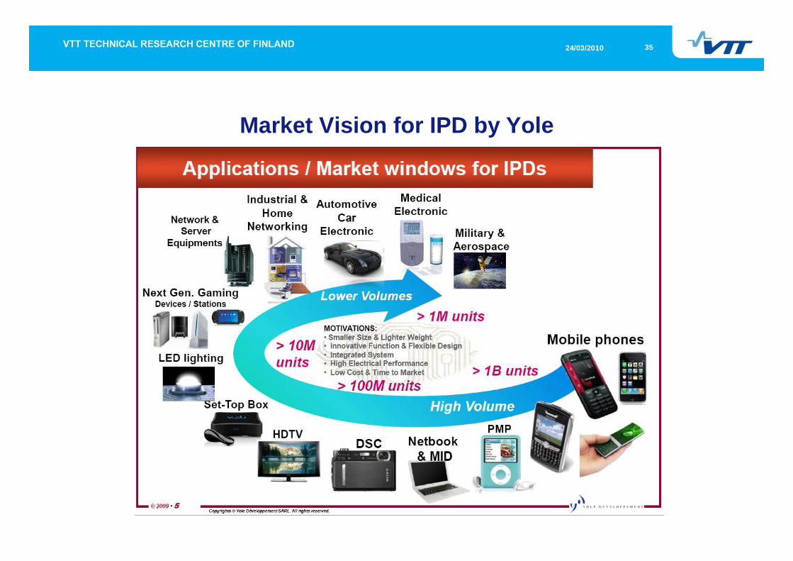
3524/03/2010
Market Vision for IPD by Yole

3624/03/2010
IPD Market Forecast by Yole

ComponentSystemProcess
TRL/MRL level 3 4 5 6 7 8Description:
Specifications:
applications and targeted markets :
Contact:
Patents:
The Heterogeneous Technology Alliance HTA
Readiness level data sheet
Thin film BAW filters for the GHz range
• High performance miniature resonator and filtertechnology for the GHz range
• Mo-AlN-Mo resonator technology on SiO2-W braggreflector, also with temperature stabilized resonators
• f ~ 1 … 5 GHz, Q > 1000, K2 ~ 6 %• Extensive simulation, design, and process development
capabilities available• AlN based technology is CMOS compatible• ZnO processing not actively maintained
Thin film bulk acoustic wave (BAW) filters
• mobile communications, novel radio systems, timingcircuits Tuomas Pensala
0
5
10
15
20
25
30850 900 950 1000 1050
Frequency (MHz)
Ref
lect
ion
S11,
Tra
nsm
issio
n S2
1 (d
B)
S21
S11EGSM
VSWR
Thin film ZnO based E-GSM Rx filter

ComponentSystemProcess
TRL/MRL level 3 4 5 6 7 8Description:
Specifications:
applications and targeted markets :
Contact:
Patents:
The Heterogeneous Technology Alliance HTA
Readiness level data sheet
Integrated Passive Devices (IPD)
• IPD process has basic building blocks like high quality factor (Q)inductors, capacitors and transmission lines
• Example high-Q components and circuits suitable to be realized withIPD: capacitors, inductors, baluns, filters, matching networks,antennas, antenna arrays, feed networks,
• Can be used as an integration platform for RF front-ends: all passiveson the IPD substrate, active devices flip chipped
• Frequency range: DC-300 GHz• Currently runing on 6” wafers
High performance Integrated Passive Devices (IPD)
• Telecommunication products: portable devices having wirelessconnectivity, base stations, radio links, …
• Power electronics, automotive, …• Defence electronics

ComponentSystemProcess
TRL/MRL level 3 4 5 6 7 8Description:
Specifications:
applications and targeted markets :
Contact:
Patents:
The Heterogeneous Technology Alliance HTA
Readiness level data sheet
IPD Inductors
• Quality factor 50-150 depending on inductance andfrequency
• Target frequency range <6 GHz• Based on thick copper metallizations on quartz or high
resistivy silicon substrates
High performance Integrated Passive Device Inductors
• Telecommunication products: portable devices having wirelessconnectivity, base stations, …
• Power electronics• Defence electronics

ComponentSystemProcess
TRL/MRL level 3 4 5 6 7 8Description:
Specifications:
applications and targeted markets :
Contact:
Patents:
The Heterogeneous Technology Alliance HTA
Readiness level data sheet
Capacitive RF-MEMS switches
• Substrate: 150 mm fused silica, Si, or hi-res Si.• Fixed and released aluminum electrodes 500-1500 nm• 50-100 nm dielectric
– = 8, C -ratio 10-20
• Wafer-level or stepper-reticle masks (5 masks)• Options:
– Sacrificial layer in two thickness levels (+ 1 mask)– Additional buried thin-film resistor (+1 mask)
• Processing, design rules, and assistance in layout basic blocks.– In-house expertise in component & system design also available
Processing flow for released aluminum RF-MEMS bridges
•1-300 GHz RF circuitry• Reconfigurable RF-circuitry, amplifiers, low-loss impedance tuners,filters, phase shifters Mikko Tuohiniemi

4124/03/2010
VTT products in LED lightning
The business in LED lighning is done in three areas: LED diodes,driving electronics, and module integrationVTT experience focuses in driving electronics and moduleintegrationThe LED diode startup OptoGaN is one of the companies in theMicronova technology parkProduct descriptions
LDMOS power electronics. The IP belongs to a technologypartner, VTT is the R&D fab. Proven state-of-art technology ata low cost. Willingness to licenciate the technology.Integrated Passive Devices (IPD) (product description givenabove), are needed in highly integrated, low-cost drivingcircuits.

4224/03/2010
LED lighting market to reach $1 billion in 2011
Source http://www.ledsmagazine.com/news/4/2/11 (02 Feb 2007)
According to a new report from Strategies Unlimited, the LED lighting marketwill grow at almost 37% over the next few years.
High-brightness LEDs have demonstrated dramatic improvements inperformance in recent years, as well as significant cost reduction. As aresult, LEDs are undergoing a period of rapid market growth in a variety oflighting applications.
According to market research firm Strategies Unlimited, in 2005 the totalmarket for high-brightness LEDs used in lighting applications was $205million.
By 2011, the total market for LEDs in lighting is forecast to grow at a CAGRof 36.9% to reach approximately $1 billion.
The largest lighting application for LEDs is architectural lighting, followed bychannel letter/contour lighting and consumer portable

ComponentSystemProcess
TRL/MRL level 3 4 5 6 7 8Description:
Specifications:
applications and targeted markets :
Contact:
Patents:
The Heterogeneous Technology Alliance HTA
Readiness level data sheet
CMOS
• Bulk or thick SOI (MEMS) substrate• 0.6 µm linewidth (gate, contact, metal)• Double metal• 0.6 µm CMOS• Vertical npn and pnp transistors, Schottky diodes• MIM capacitors
Custom integrated circuit processing
Sensor interfaces on MEMS / thinfilm sensors
Hannu [email protected]

ComponentSystemProcess
TRL/MRL level 3 4 5 6 7 8Description:
Specifications:
applications and targeted markets :
Contact:
Patents:
The Heterogeneous Technology Alliance HTA
Readiness level data sheet
LDMOS
• Based on the VTT CMOS technology and its add-onfeatures
• IP belongs to a technology partner of VTT (an SMEcompany)
• VTT is the R&D fab to developt the process, to fabricatedevice prototypes and to do pilot production at small andmedium volumes. Technology transfer (or enlargement ofthe VTT fab) needed to reach high volumes.
High-voltage, high-power RF custom integrated circuitprocessing
LED driving circuits, mirowave radars, radio-frequency andmicrowave applications up to 3 GHz (base stations etc.), pulsedlaser driving circuits Hannu Ronkainen
Several

4524/03/2010
VTT products in optical telecommunication
Optical telecommunication is a strongly increasing marketVTT has a strong portfolio of technologies for heterogeneousintegration of optoelectronical components on silicon integrationplatforms with integrated optical wave guides

ComponentSystemProcess
TRL/MRL level 3 4 5 6 7 8Description:
Specifications:
applications and targeted markets :
Contact:
Patents:
The Heterogeneous Technology Alliance HTA
Readiness level data sheet
Silicon-based optoelectronic modules
• Silicon-on-insulator (SOI) as the preferred platform• Passive SOI waveguide circuits for >1.2 µm• Optoelectronics flip-chip on SOI• RF lines and wire bonds• Through-silicon vias, also for RF & heat dissipation• Hermetic sealing with low-cost wafer-level packaging• Low-loss fiber pigtailing• From discrete devices to complicated systems on chip
Dr. Timo Aalto
• Telecom & datacom: Optoelectronic modules used astransmitters, switches, multiplexers, receivers etc.
• Optical sensors
Low-cost, silicon-based packaging technology foroptoelectronic modules
Several granted

ComponentSystemProcess
TRL/MRL level 3 4 5 6 7 8Description:
Specifications:
applications and targeted markets :
Contact:
Patents:
The Heterogeneous Technology Alliance HTA
Readiness level data sheet
Optoelectronics integration on SOI
• Au-Au thermo compression bonding as the preferred flip-chip integration method
• Possible to combine high throughput (10–100 chips/h) withhigh accuracy ( 0.1–1 µm)
• Lasers, amplifiers, modulators, detectors etc. fabricated one.g. InP, GaAs or LiNbO3 chips and then hybrid integratedon a low-loss SOI waveguide circuit
Dr. Timo Aalto
• Telecom & datacom: Optoelectronic modules used astransmitters, switches, multiplexers, receivers etc.
• Optical sensors
Flip-chip integration of optoelectronics on a silicon-on-insulator (SOI) photonic integrated circuit

ComponentSystemProcess
TRL/MRL level 3 4 5 6 7 8Description:
Specifications:
applications and targeted markets :
Contact:
Patents:
The Heterogeneous Technology Alliance HTA
Readiness level data sheet
Photonic integrated circuits on SOI
• Single-crystal Si core transparent at 1.2 µm < < 6 µm• Single mode operation for 1–12 µm core thickness• 0.1 dB/cm propagation loss• Polarisation independent and pol. maintaining options• Mirrors and special bends for minimised footprint• Passive components: Couplers, splitters, MZIs, AWGs, 3D
tapers/converters, low-loss I/O coupling etc.• Fast thermo-optic swithing/tuning (>>100 kHz)
Dr. Timo Aalto
• Telecom & datacom: Optoelectronic modules used astransmitters, switches, multiplexers, receivers etc.
• Optical sensors
Customised waveguide circuits based on a library ofcomponents developed for silicon-on-insulator (SOI)
Several granted

ComponentSystemProcess
TRL/MRL level 3 4 5 6 7 8Description:
Specifications:
applications and targeted markets :
Contact:
Patents:
The Heterogeneous Technology Alliance HTA
Readiness level data sheet
Wavelength (de)multiplexers on SOI
• Asymmetric Mach-Zehnder interferometers• Arrayed waveguide gratings• Fabry-Perot resonators• Ring resonators• Dense-to-coarse wavelength spacing (25 1000 GHz)• Customised transmission spectra (e.g. flat-top)• Typical AWG insertion loss 4.5 6 dB• Special designs for reduced footprint (e.g. mirror AWG)
Dr. Timo Aalto
• Telecom & datacom: Optoelectronic modules used astransmitters, switches, multiplexers, receivers etc.
• Optical sensors
Customised wavelength (de)multiplexers integrated onsilicon-on-insulator (SOI)
Granted
5024/03/2010
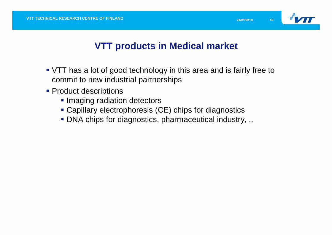
VTT products in Medical market
VTT has a lot of good technology in this area and is fairly free tocommit to new industrial partnershipsProduct descriptions
Imaging radiation detectorsCapillary electrophoresis (CE) chips for diagnosticsDNA chips for diagnostics, pharmaceutical industry, ..

ComponentSystemProcess
TRL/MRL level 3 4 5 6 7 8Description:
Specifications:
applications and targeted markets :
Contact:
Patents:
The Heterogeneous Technology Alliance HTA
Readiness level data sheet
Edgeless silicon detector
Large area pixel or strip edgeless detector having ~1m inactive region at the edge. Possibility for thin and thick
detectors on 150 mm process line.
16 September 2009
• Depletion up to the edge of the detector• ~1 m inactive region at the edge• Detector thickness: from 10 m up to 1 mm• Variables of the active edge distance
– Leakage current: ~50-80 nA/cm2
– Capacitance: 0.5-1 nF/cm2
– Breakdown voltage: 150-250 V• Large area detector up to 10x10 cm2
• UBM metallization and flip-chip bump bonding
• High energy physics• Medical imaging• Crystallography
Existing IP
Dr. Juha [email protected]

ComponentSystemProcess
TRL/MRL level 3 4 5 6 7 8Description:
Specifications:
applications and targeted markets :
Contact:
Patents:
The Heterogeneous Technology Alliance HTA
Readiness level data sheet
Custom Devices for Radiation Sensing
• Si & CdTe• Low leakage current• Low capacitance• High breakdown voltage• Pad diodes, strip and pixel detectors• Double sided processing
Dr. Simo Eränen
• UV, Vis & NIR light sensing
• x-rays & gammas
• energetic particles
Custom designed semiconductor devices for instrumentsand science

ComponentSystemProcess
TRL/MRL level 3 4 5 6 7 8Description:
Specifications:
applications and targeted markets :
Contact:
Patents:
The Heterogeneous Technology Alliance HTA
Readiness level data sheet
DRIE glass etching
• 0-400 µm deep microfluidic trenches with arbitraryshape
• Positive aspect ratio 1:10, negative 3:1• Several suitable masking schemes depending on
device requirements• Available for fused silica and Pyrex
Dr. Kai Kolari
• Microfluidics
• MEMS sensors and actuators
High aspect ratio glass etching for microfluidics andMEMS

ComponentSystemProcess
TRL/MRL level 3 4 5 6 7 8Description:
Specifications:
applications and targeted markets :
Contact:
Patents:
The Heterogeneous Technology Alliance HTA
Readiness level data sheet
Silicon microfluidic filter
• Lateral sieving: High aspect ratio pillars• Vertical sieving: Perforated silicon or silicon dioxide
membranes
Ari Hokkanen
• Sample preparation, concentration, immobilisation
• Particle and cell filtering
• LC, GC, SPE etc.
Pillar and membrane filters for microfluidics

ComponentSystemProcess
TRL/MRL level 3 4 5 6 7 8Description:
Specifications:
applications and targeted markets :
Contact:
Patents:
The Heterogeneous Technology Alliance HTA
Readiness level data sheet
Silicon-glass microchip for PCR
• Integrated heating and temperature measurementelements
• Silicon-glass microchip• Microfluidic interface for microfluidic and electrical
connections
Ari Hokkanen
• DNA diagnostics
DNA amplification on silicon-glass microchip
Patent pending

ComponentSystemProcess
TRL/MRL level 3 4 5 6 7 8Description:
Specifications:
applications and targeted markets :
Contact:
Patents:
The Heterogeneous Technology Alliance HTA
Readiness level data sheet
Microchip capillary electrophoresis
• Silicon-glass microchip• Microfluidic sieves for sample preparation• Option to use beads and magnetic particles in
sample concentration• System interface for microfluidic and electrical
connections
Ari Hokkanen
• diagnostics
• process monitoring (also on-line)
• environmental monitoring
Electrophoretic separation of molecules in silicon
Patent pending

ComponentSystemProcess
TRL/MRL level 3 4 5 6 7 8Description:
Specifications:
applications and targeted markets :
Contact:
Patents:
The Heterogeneous Technology Alliance HTA
Readiness level data sheet
Microfluidic measurement system
• Silicon-glass and polymer microfluidic chips• Easy chip replacement• Connections:
– External fluidics– Electrical– Optical measurements
Ari Hokkanen
• diagnostics
• process monitoring
• environmental monitoring
Measurement interface for Lab-On-Chips / Biochips
Patent pending

ComponentSystemProcess
TRL/MRL level 3 4 5 6 7 8Description:
Specifications:
applications and targeted markets :
Contact:
Patents:
The Heterogeneous Technology Alliance HTA
Readiness level data sheet
Microchips for monitoring cell activity
• Au, Ag, Ti and TiN thin film electrodes• 600 - 200 µm thick transparent glass chips for
microscopy
Ari Hokkanen
• Patch clamp - ion channel measurements for cells
• Cell stimulation
Electrical measurements for living cells
ComponentSystemProcess
TRL/MRL level 3 4 5 6 7 8Description:
Specifications:
applications and targeted markets :
Contact:
Patents:
The Heterogeneous Technology Alliance HTA
Readiness level data sheet
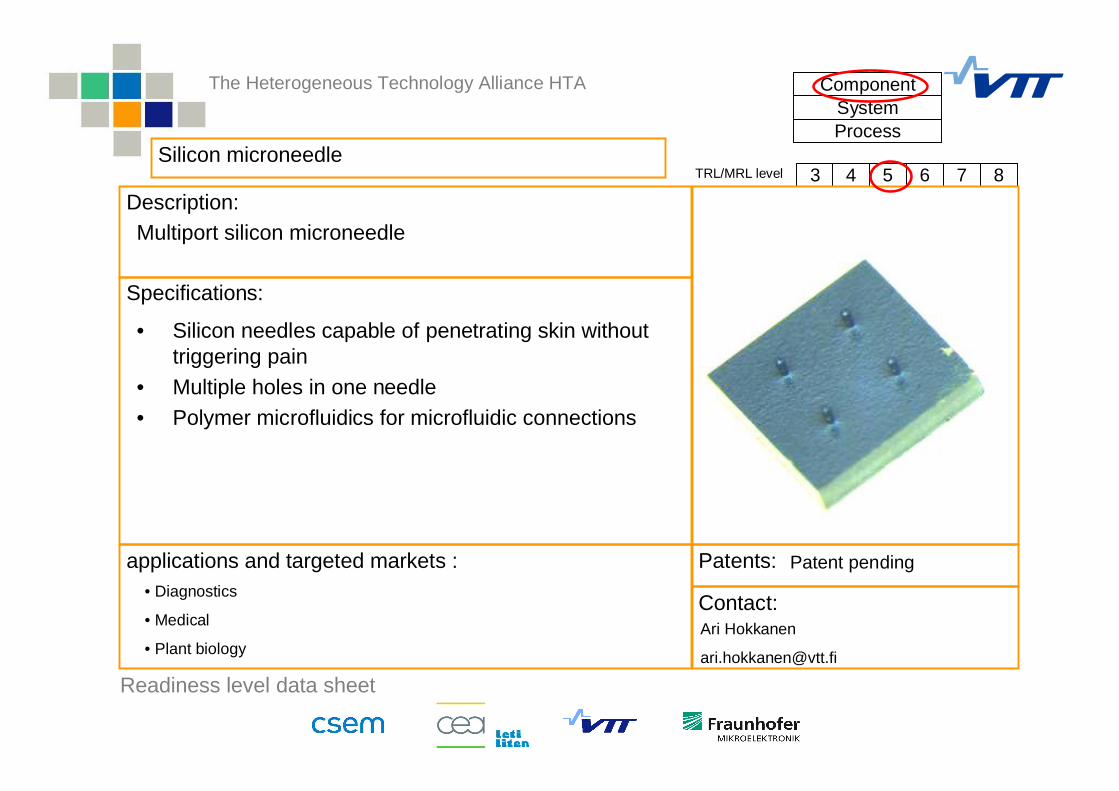
Silicon microneedle
• Silicon needles capable of penetrating skin withouttriggering pain
• Multiple holes in one needle• Polymer microfluidics for microfluidic connections
Ari Hokkanen
• Diagnostics
• Medical
• Plant biology
Multiport silicon microneedle
Patent pending

6024/03/2010
Fit to the VTT strategy
VTT has produced a large number of state-of-art research resultswith a high business potential and a short time-to-marketVTT needs more industrial partners to commercialize itstechnologyJoint ventures are seen as an attractive tool for commercializationVTT has large clean rooms for micro and nanotechnology andthere is a lot of free capacityThe VTT clean rooms are of the quality suitable for industrialproduction.VTT has initiated in Jan 2010 an active campaign, led by Prof.Aarne Oja, to search for new industrial partners.It is expected that by 2011 new industrial partnerships will occupyall available capacity of the VTT clean rooms

6124/03/2010
Summary of collaboration possibilities between VTTand potential new industrial partners
R&D project performed by VTTEstablisment of a joint venture (NewCo) between the Partner, VTTand potential third parties
NewCo could located in the Micronova technology parkAccess to the microtechnology infrastructureFloor space available in the VTT clean room forprojects/productionOffice space availableAccess rights on similar conditions as for the other companiesin the Micronova technology park

6224/03/2010
Thank you for your attention!
6324/03/2010
VTT creates business fromtechnology

6424/03/2010
APPENDIX: Technology Readiness Levels in the National Aeronautics and Space Administration(NASA)(Source: Mankins (1995), Technology Readiness Levels: A White Paper)
At this level, the fidelity of the component and/or breadboard being testedhas to increase significantly. The basic technological elements must beintegrated with reasonably realistic supporting elements so that the totalapplications (component-level, sub-system level, or system-level) can betested in a 'simulated' or somewhat realistic environment.
5. Component and/or breadboard validation in relevant environment
Following successful "proof-of-concept" work, basic technologicalelements must be integrated to establish that the "pieces" will worktogether to achieve concept-enabling levels of performance for acomponent and/or breadboard. This validation must be devised tosupport the concept that was formulated earlier, and should also beconsistent with the requirements of potential system applications. Thevalidation is "low-fidelity" compared to the eventual system: it could becomposed of ad hoc discrete components in a laboratory.
4. Component and/or breadboard validation in laboratory environment
At this step in the maturation process, active research and development(R&D) is initiated. This must include both analytical studies to set thetechnology into an appropriate context and laboratory-based studies tophysically validate that the analytical predictions are correct. Thesestudies and experiments should constitute "proof-of-concept" validation ofthe applications/concepts formulated at TRL 2.
3. Analytical and experimental critical function and/or characteristic proofof concept
Once basic physical principles are observed, then at the next level ofmaturation, practical applications of those characteristics can be'invented' or identified. At this level, the application is still speculative:there is not experimental proof or detailed analysis to support theconjecture.
2. Technology concept and/or application formulated
This is the lowest "level" of technology maturation. At this level, scientificresearch begins to be translated into applied research and development.
1. Basic principles observed and reported
DescriptionTechnology Readiness Level

6524/03/2010
In almost all cases, the end of last 'bug fixing' aspects of true'system development'. This might include integration of newtechnology into an existing system. This TRL does not includeplanned product improvement of ongoing or reusable systems.
9. Actual system 'flight proven' through successful missionoperations
In almost all cases, this level is the end of true 'systemdevelopment' for most technology elements. This might includeintegration of new technology into an existing system.
8. Actual system completed and 'flight qualified' through test anddemonstration (ground or space)
TRL 7 is a significant step beyond TRL 6, requiring an actualsystem prototype demonstration in a space environment. Theprototype should be near or at the scale of the planned operationalsystem and the demonstration must take place in space.
7. System prototype demonstration in a space environment
A major step in the level of fidelity of the technology demonstrationfollows the completion of TRL 5. At TRL 6, a representative modelor prototype system or system - which would go well beyond adhoc, 'patch-cord' or discrete component level breadboarding -would be tested in a relevant environment. At this level, if the only'relevant environment' is the environment of space, then themodel/prototype must be demonstrated in space.
6. System/subsystem model or prototype demonstration in arelevant environment (ground or space)
Source: http://en.wikipedia.org/wiki/Technology_readiness_level#TRL_assessment_tools